

Page 1
Global LCD Panel Exchange Center
TECHNICAL DATA
CONTENTS
TX36D88VC1CAA
www.panelook.com
Hitachi Displays, Ltd.
Date; Sep. 18, 2007
No.
— DPBCL0001618-1
—
—
1 DPBCL0001618-1
2 DPBCL0001618-1
3 DPBCL0001618-1
4 DPBCL0001618-1
5 DPBCL0001618-1
7 DPBCL0001618-1
8 DPBCL0001618-1
9 DPBCL0001618-1
10
COVER 1-1/1
RECORD OF REVISION 2-1/1
APPLICATIONS 3-1/1
ABSOLUTE MAXIMUM RATINGS 4-1/2 - 2/2
OPTICAL CHARACTERISTICS 5-1/2 - 2/2
ELECTRICAL CHARACTERISTICS 6-1/1
BLOCK DIAGRAM 7-1/1
INTERFACE PIN CONNECTION 8-1/4 - 4/4
INTERFACE TIMING 9-1/4 - 4/4
DIMENSIONAL OUTLINE 10-1/1
DESIGNATION OF LOT MARK 11-1/2 - 2/2
COSMETIC SPECIFICATIONS 12-1/3 - 3/3
PRECAUTIONS 13-1/4 - 4/4
DPBCL0001618-1
DPBCL0001618-1
DPBCL0001618-16
DPBCL0001618-1
PageSheet No.Item
Hitachi Displays, Ltd. DPBCL0001618-1
One step solution for LCD / PDP / OLED panel application: Datasheet, inventory and accessory!
Page
1-1/1
www.panelook.com
Page 2
Global LCD Panel Exchange Center
RECORD OF REVISION
The upper section : Before revision
The lower section : After revision
Sheet No. Page
www.panelook.com
SummaryDate
Date PageHitachi Displays, Ltd. Sep. 18, 2007 DPBCL0001618-1
One step solution for LCD / PDP / OLED panel application: Datasheet, inventory and accessory!
2-1/1
www.panelook.com
Page 3

Global LCD Panel Exchange Center
APPLICATIONS
This specification is applied to the following TFT Liquid Crystal Display Module
with Back-light unit and LVDS (Low Voltage Differential Signaling) Interface.
Note: Inverter device for Back-light is not built in and so it needs to
be prepared on your side.
www.panelook.com
Type name
Display Area : (H)285.7 × (V)214.3 [mm]
Display Pixels : (H)1,024 × (V)768 pixels
(Display Dots) (H(1024 × 3) × V768 [dots])
Power Supply Voltage : 3.3 V
Pixel Pitch : (H)0.279 × (V)0.279 [mm]
Color Pixel Arrangement : R•G•B Vertical Stripe
Display Mode : Transmissive &
Color Number : 262k Colors
Direction with Wider : Lower side of 6 o'clock
Viewing Angle
: TX36D88VC1CAA
Normally White Mode
(Azimuth I = 270°)
Dimensions Outlines : (H)298.5 × (V)225.5 typ. × (t)6.0max [mm]
Weight : 480typ. [g]
Interface : 1ch-LVDS
Back-light : One Cold Cathode Fluorescent Lamp
(Lower side)
Back-light inverter is not contained in Module.
Date PageHitachi Displays, Ltd. Sep. 18, 2007 DPBCL0001618-1
3-1/1
One step solution for LCD / PDP / OLED panel application: Datasheet, inventory and accessory!
www.panelook.com
Page 4

Global LCD Panel Exchange Center
1. ABSOLUTE MAXIMUM RATINGS
1.1 ENVIRONMENTAL ABSOLUTE MAXIMUM RATINGS
Item
Ambient Temperature 0 40 -20 60 °C 1)
Humidity 2) 2) %RH 1)
Vibration – (0.5G) – (2G)
Shock – (3G) – (50G)
Corrosive Gas Not Acceptable Not Acceptable –
Illumination at
LCD Surface
Notes 1) Environmental temperature and humidity of this unit, not of system installed with this unit.
At low temperature the brightness of CFL drop and the life time of CFL become to be short.
2) Ambient temp. Ta d 40°C : 85%RH MAX. without condensation.
Ta > 40°C : Absolute humidity must be lower than the saturated vapor of
3) Vibration frequency : 20~50Hz. (Except resonance frequency) 3min/cyc
4) 7ms of pulse width.
5) With mounting protective spacer (ref. page 4-2/2)
www.panelook.com
Operating Storage
Min. Max. Min. Max.
4.9
29.4
––
85%RH at 40°C. Without condensation.
50,000
19.6
490
50,000
Unit
m/s
m/s
lx
Note
2
2
3), 5)
4), 5)
1.2 ELECTRICAL ABSOLUTE MAXIMUM RATINGS
(1) TFT Liquid Crystal Display Module Vss=0V
Item Symbol Min. Max. Unit Note
V
V
V
ESD0
ESD1
DD
0 4.0 V
±100 V 1), 2)
±8 kV 1), 3)
Power Supply Voltage
Electrostatic Durability
Notes 1) Discharge circuit: 200pF-250:, Surrounding: 25°C-70%RH.
2) The specification is applicable to I/F Connector pins.
3) The specification is applicable to metal bezel and LCD glass.
(2) Back Light unit GND=0V
ITEM Symbol Min. Max. Unit
Lamp Current
Lamp Voltage
I
L
V
L
0 7.0 mArms
0 2,000 Vrms
Hitachi Displays, Ltd. Sep. 18, 2007 DPBCL0001618-1
Date Page
One step solution for LCD / PDP / OLED panel application: Datasheet, inventory and accessory!
4-1/2
www.panelook.com
Page 5
Global LCD Panel Exchange Center
A
A
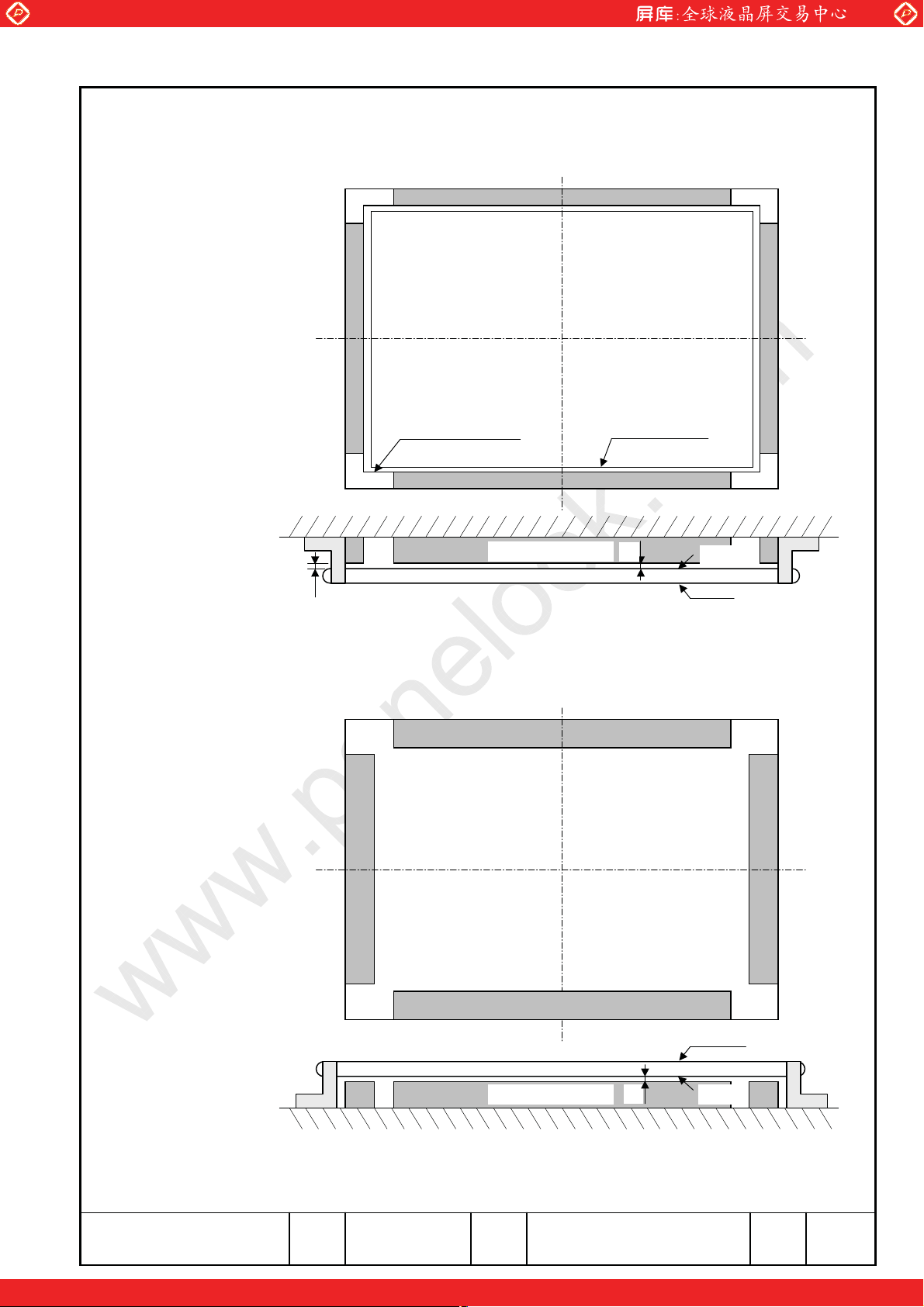
Adding protective spacer at shock & vibration test
(1) This protective
spacer is to be added
at shock and vibration
test on the front side
www.panelook.com
(2) This protective spacer
is to be added shock and
vibration test on the
back side
Window of Bezel
Protective Spacer
(1)
Display Area
(1)
Front
Back
Front
Protective Spacer
(1)
Back
Sh.
No.
One step solution for LCD / PDP / OLED panel application: Datasheet, inventory and accessory!
PageHitachi Displays, Ltd. Sep. 18, 2007 DPBCL0001618-1Date
4-2/2
www.panelook.com
Page 6
Global LCD Panel Exchange Center
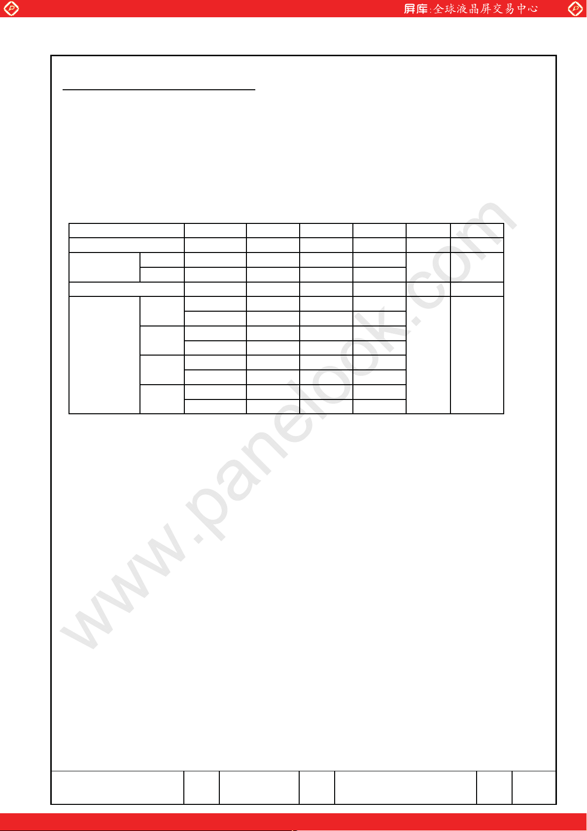
2. OPTICAL CHARACTERISTICS
The following items are measured on the conditions that this unit operation (TFT panel
and Back-light) and measuring systems are stable. (more than 30minites' operation)
The ambient light excluding The Back-light unit is nothing.
•Measuring equipment : TOPCON BM-7, Prichard 1980A, or equivalent
•Measuring point : Active area center
Item Symbol Min. Typ. Max. Unit Note
Contrast Ratio CR – 150 – – 1)
Response Rise tr – 50 –
Time Fall tf – 30 –
Brightness (white) Bwh – 150 –
Red
Color of CIE y – 0.56 – –
Green
Blue
White
www.panelook.com
Temperature of LCD=25°C, VDD=3.3V, fV=60Hz, IL=6.0mA
ms 2)
2
cd/m
x – 0.58 –
y – 0.33 –
x – 0.30 –
x – 0.15 –
y – 0.14 –
x – 0.32 –
y – 0.33 –
Hitachi Displays, Ltd. Sep. 18, 2007 DPBCL0001618-1
Date Page
One step solution for LCD / PDP / OLED panel application: Datasheet, inventory and accessory!
5-1/2
www.panelook.com
Page 7
Global LCD Panel Exchange Center
f
Notes 1) Definition of Contrast Ratio (CR)
CR =
2) Definition of Response Time
Brightness when displaying White raster
Brightness when displaying Black raster
These Brightness is measured on the center of screen.
* Measurement in the darkroom.
www.panelook.com
Optical Response
Relative
luminance
100
90
10
%
tr t
0
Sh.
No.
One step solution for LCD / PDP / OLED panel application: Datasheet, inventory and accessory!
PageHitachi Displays, Ltd. Sep. 18, 2007 DPBCL0001618-1Date
5-2/2
www.panelook.com
Page 8

Global LCD Panel Exchange Center
3. ELECTRICAL CHARACTERISTICS
3.1 TFT LIQUID CRYSTAL DISPLAY MODULE Ta=25°C, Vss=0V
Power Supply Voltage
Differential Input Voltage
for LVDS Receiver Threshold
Power Supply Current
Vsync Frequency
Hsync Frequency
DCLK Frequency
Notes 1) VCM=+1.25V
fv=60Hz, f
2)
Typical value is measured when displaying vertical 64 gray scale.
Maximum is measured when displaying Vertical-stripe (Black-Gray 7).
=65MHz, VDD=3.3V, DC Current.
CLK
DC Ampere Meter
V
DD
Hi
Lo
www.panelook.com
Symbol
V
V
V
I
f
f
f
CLK
I
DD
DD
IH
IL
DD
V
H
V
V
Min.Item
3.0
– – +100
-100
–
–
–
–
TFT/LCM
DD
SS
Typ.
3.3
–
300
60
48.5
65
Max. Unit Note
3.6
–
600
65
52.4
67
V
mV 1)
mA
Hz
kHz
MHz
2), 3)
4)
4)
4)
Current capacity for V
3)
4) For LVDS Transmitter Input
power source should be larger than 2A.
DD
3.2 BACK-LIGHT UNIT Ta=25°C
Item Symbol Min. Typ. Max. Unit Note
Lamp Current
Lamp Voltage
Frequency
I
L
V
L
f
L
Starting Lamp Voltage Vs Vrms
Notes 1) Higher IL cause the short life time of CFL.
2) DC current cause irregular fluorescence and the short life of CFL.
3) Lamp frequency may produce interference with Hsync frequency,
causing beat or flicker on the display. There fore lamp frequency
shall be as different as possible from Hsync frequency, to avoid interference.
4) Starting Lamp Voltage applied be more than Vs (Min).
5) Ta=10°C
6) Reducing Lamp current increases Lamp voltage and generally increases Lamp frequency.
So all the parameters of an inverter should be carefully designed so as not to
produce to much leakage current from high-voltage output of the inverter.
7) Must be high considering to the loss of the ballast capacitor in the inverter.
3.5 5.0 6.0 mArms
– – 11 mA0-peak
1), 2), 6)
– 650 – Vrms
50 – 70 kHz 3)
1100 – – 4)
1400 – – 4), 5), 7)
Sh.
No.
One step solution for LCD / PDP / OLED panel application: Datasheet, inventory and accessory!
PageHitachi Displays, Ltd. Sep. 18, 2007 DPBCL0001618-1Date
6-1/1
www.panelook.com
Page 9
Global LCD Panel Exchange Center
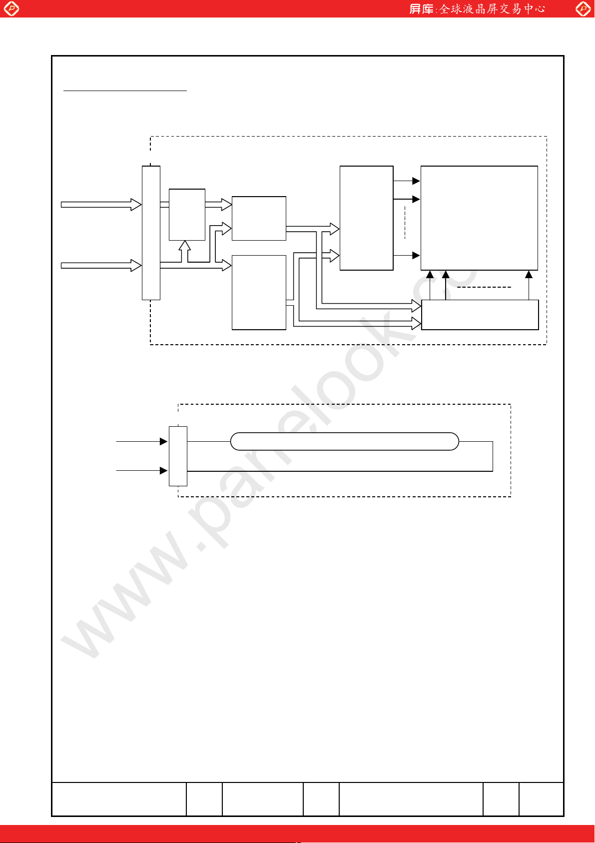
4. BLOCK DIAGRAM
4.1 TFT LIQUID CRYSTAL DISPLAY MODULE
Connector
CN1 G1
Timing signal
Display data
LVDS
Receiver
www.panelook.com
Timing
Converter
Gate
Driver
G2
TFT-LCD
DC Power
supply
4.2 BACK-LIGHT UNIT
Connector
V
L
GND
CN2
LCD
Drive
Circuit
Lamp
G768
D1
D2
D3072
Drain Driver
Date PageHitachi Displays, Ltd. Sep. 18, 2007 DPBCL0001618-1
Sh.
No.
One step solution for LCD / PDP / OLED panel application: Datasheet, inventory and accessory!
7-1/1
www.panelook.com
Page 10

Global LCD Panel Exchange Center
5. INTERFACE PIN CONNECTION
5.1 TFT LIQUID CRYSTAL DISPLAY MODULE
CN1 <<JAE FI-SEB20P-HF13 or equivalent>>
Pin No. Symbol Function
1 VDD Power Supply 3.3V nominal
2 VDD Power Supply 3.3V nominal
3 VSS Ground
4 VSS Ground
5 Rin0- Receiver Signal (-)
6 Rin0+ Receiver Signal (+)
7 VSS Ground
8 Rin1- Receiver Signal (-)
9 Rin1+ Receiver Signal (+)
10 VSS Ground
11 Rin2- Receiver Signal (-)
12 Rin2+ Receiver Signal (+)
13 VSS Ground
14 CLK- Clock Signal (-)
15 CLK+ Clock Signal (+)
16 VSS Ground
17 – NC
18 – NC
19 VSS Ground
20 VSS Ground
Notes 1) All VSS pins should be connected to GND (0V).
Metal bezel is connected internally to VSS.
2) All VDD pins should be connected to +3.3V.
3) All NC pins should be kept Open.
www.panelook.com
5.2 BACK-LIGHT UNIT
CN2 <<JST BHSR-02VS-1>>
Pin No. Symbol Function
1 VL Power Supply
2 GND GND (0V)
One step solution for LCD / PDP / OLED panel application: Datasheet, inventory and accessory!
PageHitachi Displays, Ltd. Sep. 18, 2007 DPBCL0001618-1Date
8-1/4
www.panelook.com
Page 11

Global LCD Panel Exchange Center
LVDS INTERFACE
PC Side TFT-LCD Side
www.panelook.com
CN1
2) 1)
R0~R5
G0~G5
B0~B5
Hsync
Vsync
DTMG
CLK
Host
Graphics
Controller
6
6
6
TFT
Parallel-to-LVDS
PLL
IN0+
IN0IN1+
IN1IN2+
IN2-
CLK+
CLK-
LVDS-to-TTL
PLL
6
6
6
Parallel
R0~R5
G0~G5
B0~B5
Hsync
Vsync
DTMG
LCD Panel
Controller
CLK
Notes 1) LVDS cable impedance is 100 ohms per signal line when two are used differentially...
2) Transmitter: TI SN75LVDS84, or equivalent.
Transmitter is not contained in Module.
Date PageHitachi Displays, Ltd. Sep. 18, 2007 DPBCL0001618-1
Sh.
No.
One step solution for LCD / PDP / OLED panel application: Datasheet, inventory and accessory!
8-2/4
www.panelook.com
Page 12

Global LCD Panel Exchange Center
LVDS Input Signal
V
V
V
www.panelook.com
Rin0
Rin1
Rin2
diff=0V
G0 R5 R4 R3 R2 R1 R0
B1 B0 G5 G4 G3 G2 G1
DTMG Vsync Hsync B5 B4 B3 B2
Prior cycle Signal for 1 DCLK cycle Next cycle
Pin connection in case of using
TI SN75LVDS84
INPUT Transmitter Interface connecter (CN1)
SIGNAL PC Module
R0 IN0(44)
R1 IN1(45) OUT0+ IN0+
L R2 IN2(47)
R3 IN3(48)
D R4 IN4(1)
S R5 IN5(3) OUT0- IN0-
G0 IN6(4)
G1 IN7(6)
G2 IN8(7) OUT1+ IN1+
G3 IN9(9)
G4 IN10(10)
G5 IN11(12)
B0 IN12(13) OUT1- IN1B1 IN13(15)
B2 IN14(16)
B3 IN15(18) OUT2+ IN2+
B4 IN16(19)
B5 IN17(20)
HSYNC IN18(22)
VSYNC IN19(23) OUT2- IN2DTMG IN20(25)
DCLK CLK IN(26) CLK OUT+ CLK IN+
CLK OUT- CLK IN-
Note 1) The ( ) valve of the transmitter show IC pin No.
diff=0VCLK+
Sh.
No.
One step solution for LCD / PDP / OLED panel application: Datasheet, inventory and accessory!
PageHitachi Displays, Ltd. Sep. 18, 2007 DPBCL0001618-1Date
8-3/4
www.panelook.com
Page 13

Global LCD Panel Exchange Center
RELATIONSHIP BETWEEN DISPLAY COLORS AND INPUT DATA
www.panelook.com
Color
Basic
Color
Red
Green
Input data
MSB LSB MSB LSB MSB LSB
Black 0
Red (63) 000000
Green (63) 0
Blue (63) 111111
Cyan 1
Magenta 111111
Yellow 0
White 111111
Black 0
Red (1) 0
Red (2) 0
…
…
Red (61) 0
Red (62) 000000
Red (63) 0
Black 0
Green (1) 0
Green (2) 0
…
…
111111
000000
111111
111111
000001
000010
…
…
111101
111110
000000
000000
000000
…
…
R Data G Data B Data
G1 G0G5 G4 G3 G2R0R4 R3 R2 R1
00000000000000
000000
11001111000000
000000
11111111000000
000000
11001111111111
111111
0000000000000
0
00000000
00000000
…
…
…
…
…
…
…
…
…
…
…
…
…
…
…
…
…
…
…
…
…
…
…
…
…
…
…
…
…
…
…
…
…
…
…
…
…
…
…
…
…
…
…
…
…
…
…
00000000
000000
0000000111111
00000000
01000000
10000000
…
…
…
0
…
…
00
0
00
0
11
1
00
0
000
000
000
…
…
…
…
…
…
000
000
000
000
000
…
…
…
…
…
…
B0B3 B2 B1B5 B4R5
…
…
…
…
Green (61) 000000
Green (62) 0
Green (63) 000000
Black 0
Blue (1) 1
Blue (2) 0
…
Blue
Notes 1) Definition of gray scale :
Color (n) --- number in parenthesis indicates gray scale level.
Larger number corresponds to brighter level.
2) Data Signal : 1: High, 0: Low
…
Blue (61) 1
Blue (62) 0
Blue (63) 1
000000
000000
000000
000000
…
…
…
…
…
…
…
…
…
…
…
…
000000
000000
000000
…
…
…
…
…
…
011111
10001111000000
111111
0000000000000
00000000
00000000
…
…
…
…
010000
010000
001
0
…
…
…
…
01
01
0
000
000
001
…
…
…
…
110
111
10000
111
00
…
…
…
…
…
…
Sh.
No.
One step solution for LCD / PDP / OLED panel application: Datasheet, inventory and accessory!
PageHitachi Displays, Ltd. Sep. 18, 2007 DPBCL0001618-1Date
8-4/4
www.panelook.com
Page 14

Global LCD Panel Exchange Center
6. INTERFACE TIMING
V
V
K
V
6.1 LVDS RECEIVER TIMING
(Interface of TFT module)
Rx6
Rx5 Rx4 Rx3 Rx2 Rx1 Rx0RinX
www.panelook.com
t
t
RP4
t
RP5
t
RP6
t
RP0
t
RP1
RP3
t
RP2
CLK
RinX=(RinX+)–(RinX-) (X=0,1,2)
CLK=(CLK+)–(CLK-)
Item Symbol Min. Typ. Max. Unit Note
DCLK FREQUENCY
RinX 0 data position
(X=0,1,2) 1st data position
2nd data position
3rd data position
4th data position
5th data position
6th data position
1/t
t
t
t
t
t
t
t
CLK
PR1
PR0
PR6
PR5
PR4
PR3
PR2
t
CL
diff=0V
60 65 68 MHz
-0.49 0 +0.49
1/7t
2/7t
3/7t
4/7t
5/7t
6/7t
–0.49 1/7t
CLK
–0.49 2/7t
CLK
–0.49 3/7t
CLK
–0.49 4/7t
CLK
–0.49 5/7t
CLK
–0.49 6/7t
CLK
CLK
CLK
CLK
CLK
CLK
CLK
1/7t
2/7t
3/7t
4/7t
5/7t
6/7t
CLK
CLK
CLK
CLK
CLK
CLK
+0.49
+0.49
+0.49
+0.49
+0.49
+0.49
diff=0V
ns
Sh.
No.
One step solution for LCD / PDP / OLED panel application: Datasheet, inventory and accessory!
PageHitachi Displays, Ltd. Sep. 18, 2007 DPBCL0001618-1Date
9-1/4
www.panelook.com
Page 15

Global LCD Panel Exchange Center
V
6.2 TIMING CONVERTER TIMING
(Input timing for transmitter)
Hsync
t
SV
Vsync
t
WH
Hsync
t
HBP
DTMG
www.panelook.com
t
HP
t
WI
t
HV
t
HfP
t
VP
t
W
Vsync
t
IP
Hsync
t
VBP
DTMG
The timings except mentioned above are referred to the specifications
of your transmitter.
t
VfP
Date PageHitachi Displays, Ltd. Sep. 18, 2007 DPBCL0001618-1
Sh.
No.
One step solution for LCD / PDP / OLED panel application: Datasheet, inventory and accessory!
9-2/4
www.panelook.com
Page 16

Global LCD Panel Exchange Center
Item Symbol Min. Typ. Max. Unit Note
Hsync
Vsync
DTMG Horizontal Back Porch
Note 1)
Period
Width-Active
Setup time
Hold time
Period
Width-Active
Display lines
Display clocks
Horizontal Front Porch
Vertical Back Porch
Vertical Front Porch
t
+ t
VFP
t 3t
HP
VBP
www.panelook.com
t
t
t
t
t
t
t
t
HP
WH
t
SV
HV
t
VP
WV
t
IP
t
WI
HBP
HFP
VBP
VFP
1,142 1,344 2,400
8 136 160
-2 – –
0––
771 806 1,000
1 6 120
768 768 768
1,024 1,024 1,024
32 – 416
4––
0––
1––
t
t
t
t
t
t
t
CLK
CLK
HP
HP
CLK
CLK
HP
For Hsync
1)
Date PageHitachi Displays, Ltd. Sep. 18, 2007 DPBCL0001618-1
One step solution for LCD / PDP / OLED panel application: Datasheet, inventory and accessory!
9-3/4
www.panelook.com
Page 17

Global LCD Panel Exchange Center
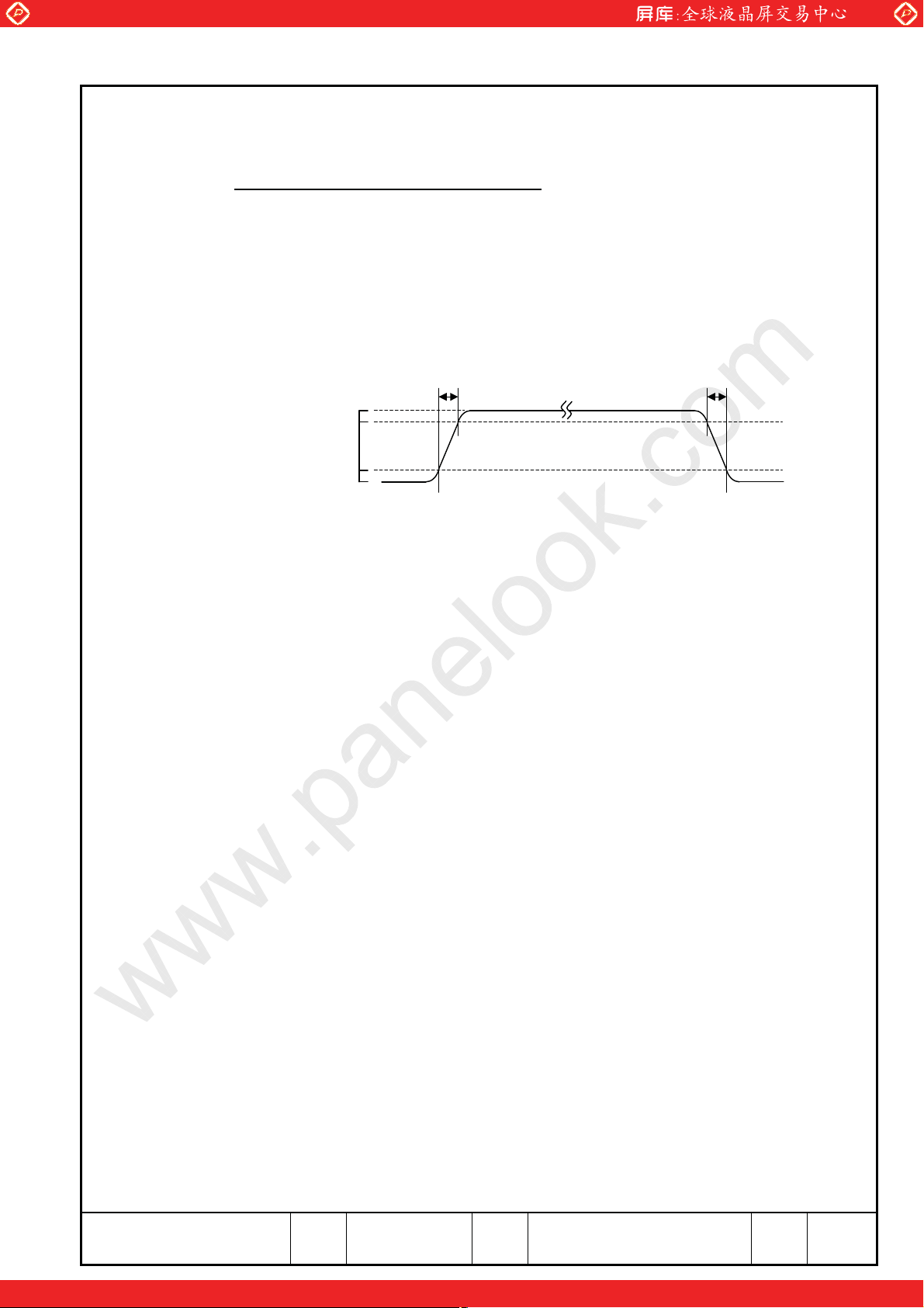
6.3 TIMING BETWEEN INTERFACE SIGNAL AND POWER SUPPLY
3.0V 3.0V
www.panelook.com
Power supply
V
(t)
DD
Interface signal
(t)
V
I
Back-Light
0V
0.8V
Note 1)
t
1t2
POWER ON
t1 d 15ms
0 < t
0 < t
2
3
0.1s d t
t
4
d 45ms
d 5ms
4
0.8V
VALID
t
3
t
Note 1)
t
t
3
5
t
6
7
t
8
ON
POWER OFF
Notes 1) t2: Hi-Z(Hi-impedace)state
2) t3: Signal transition time from Hi-Z state to Valid state specified by 3-1, 6-1 and 6-2.
3) Recommended value
Date PageHitachi Displays, Ltd. Sep. 18, 2007 DPBCL0001618-1
Sh.
No.
One step solution for LCD / PDP / OLED panel application: Datasheet, inventory and accessory!
9-4/4
www.panelook.com
Page 18

Global LCD Panel Exchange Center
www.panelook.com
One step solution for LCD / PDP / OLED panel application: Datasheet, inventory and accessory!
www.panelook.com
Page 19

Global LCD Panel Exchange Center
8. DESIGNATION OF LOT MARK
Y
8.1 LOT MARK
Lot Mark is consisted of 4 digits for production lot and 7 digits for production control.
www.panelook.com
5907
Month 2)
ear 1)
Notes
1) Year Mark 2) Month Mark Month Mark 3) Week (Days) Mark
2006 6 1 01 7 07 1~7 1
2007 7 2 02 8 08 8~14 2
2008 8 3 03 9 09 15~21 3
2009 9 4 04 10 10 22~28 4
2010 0 5 05 11 11 29~31 5
H
Optional Mark 5)
Hitachi internal use 4)
Week 3)
6061212
Serial No.
4) H Made in JAPAN
C Made in CHINA
Optional Mark for Hitachi.
5)
8.2 SERIAL NO.
Serial No. is consisted of 5 digits number (00001~99999).
Sh.
No.
PageHitachi Displays, Ltd. Sep. 18, 2007 DPBCL0001618-1Date
11-1/2
One step solution for LCD / PDP / OLED panel application: Datasheet, inventory and accessory!
www.panelook.com
Page 20

Global LCD Panel Exchange Center
8.3 LOCATION OF LOT MARK
Label is attached on the back side of module.
8.4 REV.
8.4.1 Made in JAPAN
www.panelook.com
Lot No. &
Production Control No.
8.4.2 Made in CHINA
Lot No. &
Production Control No.
TX36D88VC1CAA
CAUTION HIGH VOLTAGE
7095H 00001
REV
COLD CATHODE FLORESCENT LAMP IN COLOR LCD CONTAINS MERCURY.
PLEASE FOLLOW LOCAL ORDINANCES OR REGULATIONS FOR ITS DISPOSAL.
TX36D88VC1CAA
MADE IN JAPAN
L0 05 00 3 A 22 000001
CAUTION HIGH VOLTAGE
7095C 00001
REV
MADE IN CHINA
L0 05 00 3 A 22 000001
COLD CATHODE FLORESCENT LAMP IN COLOR LCD CONTAINS MERCURY.
PLEASE FOLLOW LOCAL ORDINANCES OR REGULATIONS FOR ITS DISPOSAL.
Date PageHitachi Displays, Ltd. Sep. 18, 2007 DPBCL0001618-1
Sh.
No.
One step solution for LCD / PDP / OLED panel application: Datasheet, inventory and accessory!
11-2/2
www.panelook.com
Page 21

Global LCD Panel Exchange Center
9. COSMETIC SPECIFICATIONS
A
9.1 CONDITIONS FOR COSMETIC INSPECTION
www.panelook.com
(1) Viewing zone
Viewing
zone
i) The figure shows the correspondence
between eyes (of inspector) and
TFT/LCD module.
•Td 45° when non-operating inspection
•Td 5° when operating inspection
ii) Inspection should be executed only
about
300mm
T
from front side, and only A-zone.
Cosmetic of B-zone and C-zone are
0
ignored.
(refer to 9.2 DEFINITION OF ZONE)
TFT/LCD module
(2) Environmental
i) Temperature : 25°C
When operating inspection, surface temperature of LCD panel
is 25°C.
ii) Ambient light : More than 800 [lx] and non-directive.
iii) Back-light : When non-operating inspection, Back-light should be off.
mbjent
light
(3) Operating inspection
Operating inspection should be done with 8 color mode (without gray scale).
9.2 DEFINITION OF ZONE
•A-zone : Display area (pixel area).
•B-zone : Area between A-zone and C-zone.
•C-zone : Metal bezel area.
A-zone
B-zone
C-zone
(Include I/F connector)
Date PageHitachi Displays, Ltd. Sep. 18, 2007 DPBCL0001618-1
Sh.
No.
One step solution for LCD / PDP / OLED panel application: Datasheet, inventory and accessory!
12-1/3
www.panelook.com
Page 22

Global LCD Panel Exchange Center
9.3 COSMETIC SPECIFICATIONS
When displaying condition is not stable (ex. at turn on or off),
the following specifications are not applied.
No. Item
1 Dot Defect 1dot 10 pcs 1), 2) 4)
Sparkle 2dots 4
mode 3dots 0
Black 2dots 4
mode 3dots 0
2 Line Defect Serious one
3 Uneven Brightness is no good.
4 Stain Inclusion W < 0.05 L: Ignore Ignore
Line shape W t 0.05
W: width (mm) < 0.08
L: length (mm) 0.08 d W 3.0 < L 0
5 Stain Inclusion D < 0.22 Ignore
Dot shape 0.22 d D < 0.50 5 pcs 7)
D: average dia.
6 Scratch on polarizer W < 0.05 L: Ignore Ignore
Line shape W t 0.05 L d 3.0 4
W: width (mm) < 0.10 3.0 < L 0
L: length (mm) 0.10 d W0
7 Polarizer Dent/Bubble D d 0.3 Ignore
/Peeling 0.3 < D d 0.5 10 pcs 8)
D: average dia.
8 Wrinkles on Polarizer Serious one
(mm) 0.50 d D0
(mm) 0.5 < D d 1.0 5
www.panelook.com
Maximum acceptable number
A-zone
density 1
1dot 10 pcs 1), 3), 4)
density 1
Total 10 pcs 1)
L d 3.0
1.0 < D 0
10
is no good.
Unit
units
pcs/I10
units
pcs/I5
pcs
pcs 8)
–
Note
1), 2), 5)
1), 2), 6)
1), 3), 5)
1), 3), 6)
––
7)
–
Date PageHitachi Displays, Ltd. Sep. 18, 2007 DPBCL0001618-1
Sh.
No.
One step solution for LCD / PDP / OLED panel application: Datasheet, inventory and accessory!
12-2/3
www.panelook.com
Page 23

Global LCD Panel Exchange Center
www.panelook.com
Notes 1) Dot Defect
2) Sparkle mode
3) Black mode
4) 1 dot
5) N dots
R G B R G B R G B The combination of the defect dot × and
R G B R G B R G B are considered as consecutive defect dots.
: Defect area > 1/2 dot
: Brightness of dot is more than 30% at Black raster. (Visible to eye)
: Brightness of dot is less than 70% at white raster. (Visible to eye)
: defect dot is isolated, not attached to other defect dot.
: N defect dots are consecutive. (N means the number of defect dots. (N t 2))
other defects () as shown in Fig. (a)
×
R G B R G B R G B : Directory adjacent to ×
RGBRGBRGB
Fig. (a)
6) Density : Number of defect dots inside of specified diameter.
7) Those stains which can be wiped out easily are acceptable.
8) Polarizer area inside of B-zone is not applied.
Date PageHitachi Displays, Ltd. Sep. 18, 2007 DPBCL0001618-1
One step solution for LCD / PDP / OLED panel application: Datasheet, inventory and accessory!
12-3/3
www.panelook.com
Page 24

Global LCD Panel Exchange Center
10. PRECAUTIONS
Please pay attention to the followings when you use this TFT/LCD module with
Back-light unit.
10.1 MOUNTING PRECAUTION
(1) You must mount Module using mounting holes (4 holes at side of Module) tightly.
(2) You should consider the mounting structure so that uneven force (ex. twisted stress)
is not applied to Module.
And the case which Module is mounted should have sufficient strength so that
external force is not transmitted directly to Module.
(3) To improve the strength of module against the mechanical shock the space between
module and the case should be less than 1.0mm.
www.panelook.com
TFT Module
case
1.0mm max.
(4) You should adopt radiation structure to satisfy the temperature specification.
(5) Acetic acid type and chlorine type materials for the cover case should not be used.
Because the former generate corrosive gas of attacking the polarizer at high
temperature and the latter causes circuit break by electro-chemical reaction.
(6) Do not touch, push or rub the exposed polarizers with glass, tweezers or anything
harder than HB pencil lead. And please do not rub by dusty clothes with chemical
treatment.
Do not touch the surface of polarizer with bare hand or greasy close.
(Some cosmetics are detrimental to the polarizer.)
(7) When the surface becomes dusty, please wipe gently with absorbent cotton.
IPA (Isopropyl Alcohol) is recommended for cleaning the adhesives used to
attach front/rear polarizers. Don't use acetone, toluene, and alcohol because
they cause chemical damage to polarizer
(8) Wipe off saliva or water drops as soon as possible. Their long time contact with
polarizer causes deformations and color fading.
(9) Do not open the case because inside circuits have not sufficient strength.
(10) Use fingerstalls of soft gloves in order to keep clean display quality,
when you handle the device for incoming inspection and assembly.
(11) Do not pull or do not fold the CFL cable.
Date PageHitachi Displays, Ltd. Sep. 18, 2007 DPBCL0001618-1
Sh.
No.
One step solution for LCD / PDP / OLED panel application: Datasheet, inventory and accessory!
13-1/4
www.panelook.com
Page 25

Global LCD Panel Exchange Center
10.2 OPERATING PRECAUTION
(1) Response time depends on the temperature. (In lower temperature, it becomes longer).
And also Transmittance and Color depend on the temperature.
(2) Brightness depends on the temperature. (In lower temperature, it becomes lower).
And in lower temperature, response time (required time that brightness is stable
after turn on) becomes longer.
(3) Optical characteristics (eg. Luminance, uniformity, color coordinate etc.)
gradually change by operating condition, especially low temperature change faster,
because LCD module has Cold Cathode Fluorescent Lamp.
(4) Be careful for condensation at sudden temperature change.
Condensation make damage to polarizer or electrical contact part.
And after fading condensation, smear or spot will occur.
(5) When fixed patterns are displayed at long times, afterimage is likely to occur.
(6)
The Module have high frequency circuit. If you need to shield the electromagnetic
noise, please do in yours.
(7)
When Back-light unit is operating, it sounds.
If you need to shield the noise, please do in yours.
(8)
Please connect the Back-light connector to the inverter circuit directly.
The long cable between CFL and the inverter may cause the brightness drop of CFL
and may cause the rise of starting lamp Voltage (VS).
(9) Do not connect or remove the module from main system with power applied.
www.panelook.com
10.3 ELECTROSTATIC DISCHARGE CONTROL
(1) Since Module is composed with electronic circuit, it is not strong to electrostatic
discharge. Make certain that treatment persons are connected to ground through
list band etc.. And don't touch I/F pin directly.
(2) When the polarizer protection film is peeled off, electrostatic discharge occurs.
Please peel it of slowly.
10.4 PRECAUTION FOR STRONG LIGHT EXPOSURE
Strong light exposure causes degradation of polarizer and color filter.
Date PageHitachi Displays, Ltd. Sep. 18, 2007 DPBCL0001618-1
One step solution for LCD / PDP / OLED panel application: Datasheet, inventory and accessory!
13-2/4
www.panelook.com
Page 26

Global LCD Panel Exchange Center
10.5 STORAGE
When storing Module as spares for long time, the following precautions are necessary.
(1) Store them in a dark place ; do not expose then to sunlight or fluorescent light.
Keep the temperature between 5°C and 35°C at normal humidity.
(2) The polarizer surface should not come in contact with any other object.
It is recommended that they be stored in the container in which they were shipped.
10.6 HANDLING PRECAUTIONS FOR PROTECTIVE FILM
(1) When the protective film is peeled off, static electricity is generated between the
film and the polarizer.
This film should be peeled off slowly and carefully by people who are electrically
grounded and with well ion-blown equipment or in such a condition, etc.
(2) The protective film is attached to the polarizer with a small amount of glue.
If some stress is applied to rub the protective film against the polarizer during
the time you peel off the film, the glue is apt to remain more on the polarizer.
So please carefully peel off the protective film without rubbing it against the polarizer.
(3) When the Module with protective film attached is stored for long time,
sometimes there remains a very small amount of glue, still on the polarizer after the
protective film is peeled off.
Please refrain from storing the Module at the high temperature and high humidity
for glue is apt to remain in these condition.
(4) The Glue may be taken for the Modules failure, but you can remove the Glue easily.
When the glue remains on the polarizer surface or its vestige is recognized,
please wipe them off with absorbent cotton waste or other soft material soaked with
IPA (Isopropyl Alcohol).
www.panelook.com
Date PageHitachi Displays, Ltd. Sep. 18, 2007 DPBCL0001618-1
One step solution for LCD / PDP / OLED panel application: Datasheet, inventory and accessory!
13-3/4
www.panelook.com
Page 27

Global LCD Panel Exchange Center
10.7 SAFETY
(1) If Module is broken, be careful to handle not to injure. (TFT/LCD and Lamp are
made of glass.)
Please wash hands sufficiently when you touch the liquid crystal coming out from
broken LCDs.
(2) As Back-light unit has high voltage circuit internal, do not open the case and do
not insert foreign materials in the case.
(3) The LCD Modules include Cold Cathode Fluorescent Lamp (CFL).
CFL contains a small amount of mercury. Please follow local ordinances or
regulations for disposal.
(4) The CFL inverter should be designed to include the function of output shutdown
in case the output over current happens due to any backlight trouble.
The shutdown function should be assured to work in abnormal condition at the
actual system.
www.panelook.com
Date PageHitachi Displays, Ltd. Sep. 18, 2007 DPBCL0001618-1
One step solution for LCD / PDP / OLED panel application: Datasheet, inventory and accessory!
13-4/4
www.panelook.com
 Loading...