

Page 1
Global LCD Panel Exchange Center
FOR MESSRS: DATE : May 31st ,2012
www.panelook.com
CUSTOMER’S ACCEPTANCE SPECIFICATIONS
TX43D50VM0BAA
Contents
No. ITEM SHEET No. PAGE
1 COVER 7B64PS 2701-TX43D50VM0BAA-1 1-1/1
2 RECORD OF REVISION 7B64PS 2702-TX43D50VM0BAA-1 2-1/1
3 GENERAL DATA 7B64PS 2703-TX43D50VM0BAA-1 3-1/2~2/2
4 ABSOLUTE MAXIMUM RATINGS 7B64PS 2704-TX43D50VM0BAA-1 4-1/1
5 ELECTRICAL CHARACTERISTICS 7B64PS 2705-TX43D50VM0BAA-1 5-1/2~2/2
6 OPTICAL CHARACTERISTICS 7B64PS 2706-TX43D50VM0BAA-1 6-1/2~2/2
7 BLOCK DIAGRAM 7B64PS 2707-TX43D50VM0BAA-1 7-1/1
8 INTERFACE PIN ASSIGNMENT 7B64PS 2708-TX43D50VM0BAA-1 8-1/5~5/5
9 TIMING CHART 7B64PS 2709-TX43D50VM0BAA-1 9-1/4~4/4
10 OUTLINE DIMENSIONS 7B64PS 2710-TX43D50VM0BAA-1 10-1/2~2/2
11 APPEARANCE STANDARD 7B64PS 2711-TX43D50VM0BAA-1 11-1/3~3/3
12 PRECAUTIONS 7B64PS 2712-TX43D50VM0BAA-1 12-1/1~2/2
13 DESIGNATION OF LOT MARK 7B64PS 2713-TX43D50VM0BAA-1 13-1/1
ACCEPTED BY: PROPOSED BY:
KAOHSIUNG OPTO-ELECTRONICS INC.
One step solution for LCD / PDP / OLED panel application: Datasheet, inventory and accessory!
SHEET
NO.
7B64PS 2701-TX43D50VM0BAA-1
PAGE
1-1/1
www.panelook.com
Page 2
Global LCD Panel Exchange Center
www.panelook.com
2. RECORD OF REVISION
DATE SHEET No. SUMMARY
KAOHSIUNG OPTO-ELECTRONICS INC.
One step solution for LCD / PDP / OLED panel application: Datasheet, inventory and accessory!
SHEET
NO.
7B64PS 2702-TX43D50VM0BAA-1
PAGE
2-1/1
www.panelook.com
Page 3
Global LCD Panel Exchange Center
www.panelook.com
3. GENERAL DATA
3.1 DISPLAY FEATURES
This module is a 17” WXGA amorphous silicon TFT. The pixel format is vertical stripe and sub pixels
are arranged as R (red), G (green), B (blue) sequentially. This display is RoHS compliant, COF (chip on
film) technology and LED backlight are applied on this display.
Part Name TX43D50VM0BAA
Module Dimensions 400.0(W) mm x 258.0(H) mm x 20.0 (D) mm typ.
LCD Active Area 369.6(W) mm x 221.76(H) mm
Pixel Pitch 0.28875(W) mm x 0.28875 (H) mm
Resolution 1280 x 3(RGB)(W) x 768(H) dots
Color Pixel Arrangement R, G, B Vertical stripe
LCD Type Transmissive Color Mode; Normally Black Mode
Display Type Active Matrix
Number of Colors 16.7M Colors
Backlight Edge Light Type with White LED
Weight 1700 typ. (g)
Interface 1-channel LVDS (LVDS:Low Voltage Differential Signaling)
Power Supply Voltage 5V for LCD; 12V for Backlight
Viewing Direction
Super Wide Version (In-Plane Switching)
KAOHSIUNG OPTO-ELECTRONICS INC.
SHEET
NO.
7B64PS 2703-TX48D50VM0BAA-1
One step solution for LCD / PDP / OLED panel application: Datasheet, inventory and accessory!
PAGE 3-1/2
www.panelook.com
Page 4
Global LCD Panel Exchange Center
www.panelook.com
3.2 APPLICATION AND OTHERS
(1) This LCD module was designed and manufactured to be used in an air-conditioned room away from
direct sunlight.
(2) This LCD module cannot be applied to an instrument which requires extremely high reliability and
safety from its functions and precision. These instruments include medical equipment which affects
life- and/or wealth-support apparatus.
(3) Any problems caused by a use with deviation from the conditions mentioned in this specification are
not included in the warranty.
(4) Maintenance
This LCD module and the aforementioned data may be changed without notice. When you demand
maintenance parts, please inquire about the changes in advance.
(5) Repair
We will replace or repair all defective modules if the relevant defect is caused by KOE. However, we
will not take any responsibilities for defective modules after the expiration of warranty period. Also, if
you access the modules for repairs, we will not warrant them either even if it is within the warranty
period.
(6) Items in this specification may be changed for improvement without prior notice. Please consult our
sales division before engineering an instrument with this LCD module.
(7) When a question arises concerning the specification, please contact our sales division.
KAOHSIUNG OPTO-ELECTRONICS INC.
SHEET
NO.
7B64PS 2703-TX48D50VM0BAA-1
One step solution for LCD / PDP / OLED panel application: Datasheet, inventory and accessory!
PAGE
3-2/2
www.panelook.com
Page 5
Global LCD Panel Exchange Center
www.panelook.com
4. ABSOLUTE MAXIMUM RATINGS
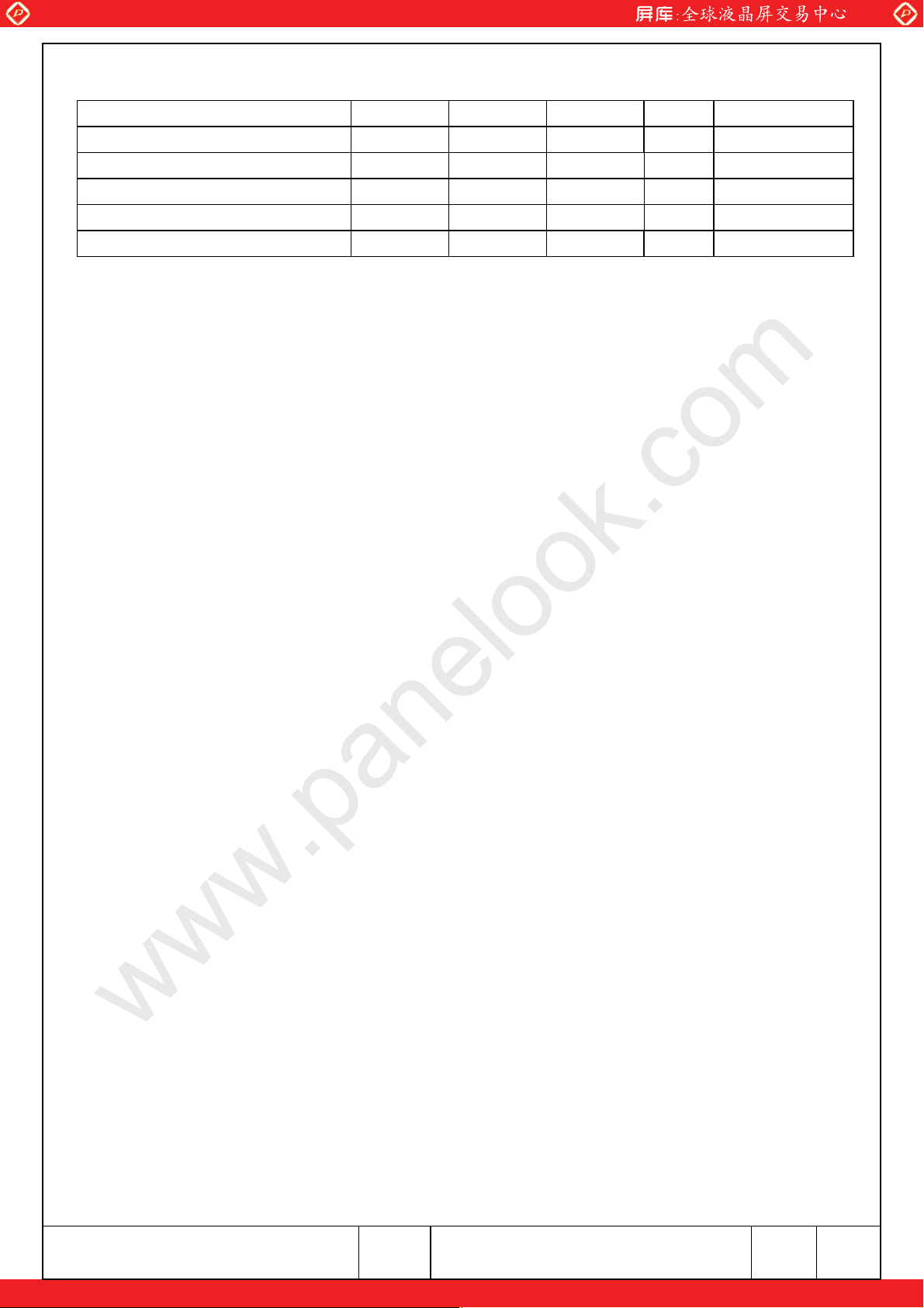
Item Symbol Min. Max. Unit Remarks
Supply Voltage VDD 0 6 V -
Input Voltage of Logic VI -0.3 3.4 V Note 1
Operating Temperature Top 0 50
Storage Temperature Tst -20 60
Backlight Input Voltage VLED - (18) V -
Note 1: It is applied to LVDS signal.
Note 2: Temperature and Humidity should be applied to the center glass surface of TFT module, not
to the system installed with a module. The temperature at the center of rear surface should be
less than 60°C on the condition of operating. Function of module is guaranteed in above
operating temperature range, but optical characteristics is specified for only 25°C operating
condition.
$
Note 2
C
$
Note 2
C
KAOHSIUNG OPTO-ELECTRONICS INC.
SHEET
NO.
7B64PS 2704-TX43D50VM0BAA-1
One step solution for LCD / PDP / OLED panel application: Datasheet, inventory and accessory!
PAGE 4-1/1
www.panelook.com
Page 6
Global LCD Panel Exchange Center
H
K
www.panelook.com
5. ELECTRICAL CHARACTERISTICS
5.1 LCD CHARACTERISTICS
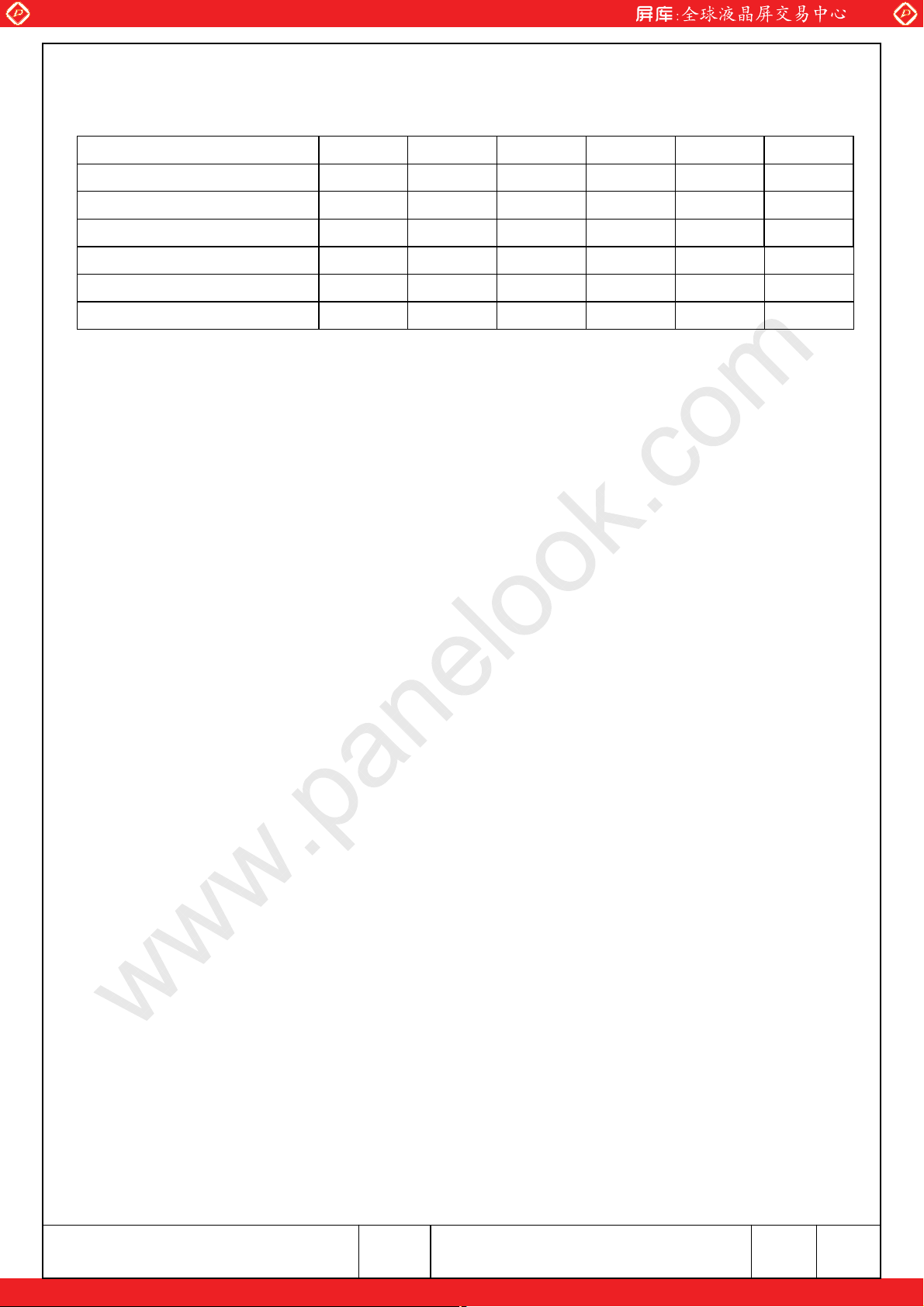
Item
Power Supply Voltage
Input Voltage of Logic
Power Supply Current IDD - 430 520 mA Note 2
Vsync Frequency
Hsync Frequency
CLK Frequency
Symbol
Min. Typ. Max. Unit Remarks
VDD
VI
f
50 60 65 Hz Note 3
v
f
44.8 47.1 52.3 KHz
f
65 66 73 MHz
CL
4.5 5 5.5 V -
-0.3 - 3.4
$
a
V -
0VVSS,25 CT
Note 3
Note 3
Note 1: It is applied to except LVDS signal.
Note 2: Temperature and Humidity should be applied to the center glass surface of TFT module, not
to the system installed with a module. The temperature at the center of rear surface should be
less than 60°C on the condition of operating. Function of module is guaranteed in above
operating temperature range, but optical characteristics is specified for only 25°C operating
condition.
Note 3: As this module contains fuse (1.0A), prepare current source that is enough for cutting current
fuse (larger than 2.5A) or set a protection circuit when a trouble happens.
Note 4: The picture on typcal current is white picture.
Note 5: When at low frequency drive, flicker may appear on screen. Please verify the flicker level before
system design.
KAOHSIUNG OPTO-ELECTRONICS INC.
One step solution for LCD / PDP / OLED panel application: Datasheet, inventory and accessory!
SHEET
NO.
7B64PS 2705-TX43D50VM0BAA-1
PAGE 5-1/2
www.panelook.com
Page 7

Global LCD Panel Exchange Center
www.panelook.com
5.2 BACKLIGHT CHARACTERISTICS
Item
Input Voltage Vin 10.8 12.0 13.2 V -
Input Current Iin - (1.36) 1.9 A Note 1
ON/OFF
Control Voltage
Brightness Control Voltage Vbc 1.0 - 3.6 V Note 2
PWM dimming signal
Input Voltage
PWM Frequency PWMf 140 150 160 Hz -
ON
OFF 0 - 0.8 V B/L=OFF
ON/OFF
PWM
Symbol
Min. Typ. Max. Unit Remarks
2.5 - 5.0 V B/L=ON
High 2.9 - 5.0 V Note 3
Low 0 - 0.9 V -
$
CT
25
a
Note 1: VIN=12.0V, VBC=3.3V or PWMf=150Hz and display pattern is a full White (Gray scale = 255
level).
Note 2: A protection fuse is built into this module. As this module contains fuse (1.0A), prepare current
source that is enough for cutting current fuse (larger than 2.5A) or set a protection circuit when
a trouble happens.
Note 3: The picture on typcal current is white picture.
VBC(Typ.) Brightness
1.0V 20%
1.3V 30%
1.5V 40%
1.8V 50%
2.0V 60%
2.3V 70%
2.5V 80%
2.8V 90%
Above 3.0V 100%
Note 4: Brightness Control (Reference value)
PWM (Typ.) Brightness
5% 5%
10% 10%
20% 20%
30% 30%
40% 40%
50% 50%
60% 60%
70% 70%
80% 80%
90% 90%
100% 100%
KAOHSIUNG OPTO-ELECTRONICS INC.
SHEET
NO.
7B64PS 2705-TX43D50VM0BAA-1
One step solution for LCD / PDP / OLED panel application: Datasheet, inventory and accessory!
PAGE 5-2/2
www.panelook.com
Page 8
Global LCD Panel Exchange Center
www.panelook.com
6. OPTICAL CHARACTERISTICS
The following optical characteristics are measured when the LCD is set alone (apart from driving
circuits and monitor cabinets) and under stable conditions. It takes about 30 minutes to reach stable
conditions. The measuring point is the center of display area unless otherwise noted.
The optical characteristics should be measured in a dark room or equivalent state.
Measuring equipment : KONICA MINOLTA: CS-2000 or equivalent.
Ambient Temperature=25±3°C, VDD=5.0V, fV=60Hz, VIN=12.0V,
and VBC=3.3V or PWM=100% (PWMf=150Hz)
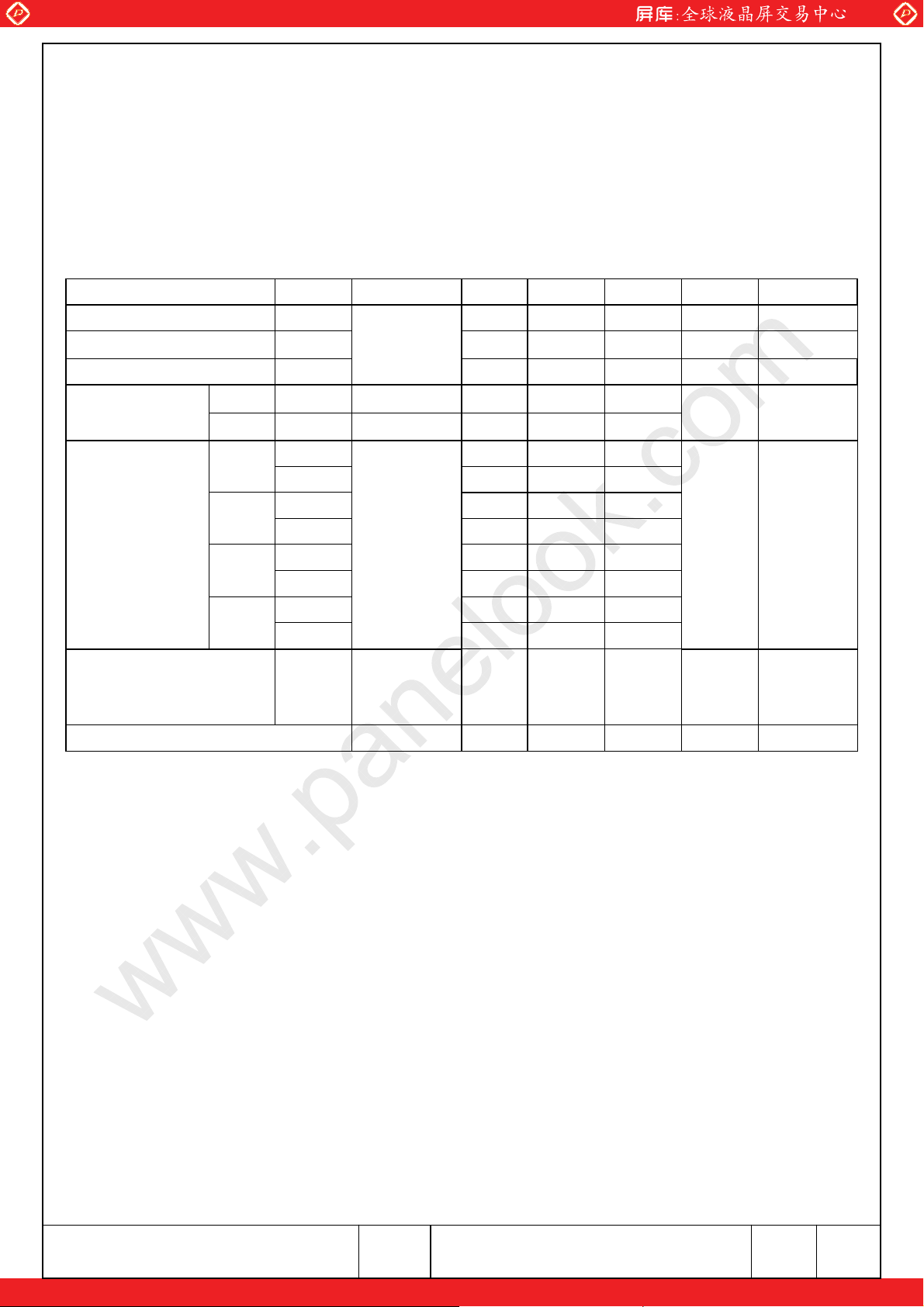
Item
Brightness of White Bwh
Brightness Uniformity
Contrast Ratio CR 700 1000 - - Note 4
Response Time
Color
Chromaticity
(CIE)
Contrast Ratio at 85± CR 85±
NTSC Ratio
Rise ton
Fall toff
Red
Green
Blue
White
Symbol
Buni 75 - - % Note 3
X
Y 0.298 0.328 0.358
X 0.280 0.310 0.340
Y 0.588 0.618 0.648
X 0.118 0.148 0.178
Y 0.025 0.055 0.085
X 0.283 0.313 0.343
Y 0.299 0.329 0.359
Condition Min. Typ. Max. Unit Remarks
420 500 -
$
0
T
ton - 12 20
toff - 10 18
0.621 0.651 0.681
$
0
T
$
85
T
I
T
,90,0$$
$$
270,018
$
0
- 72 - % -
10 - - - -
2
cd/m
Note 1,2
ms Note5
- Note 6
Note 1: The brightness is measured from the panel center point, P5 in Fig. 6.2, for the typical value.
Note 2: Brightness of white is measured by LCM is light up after 30 minutes .
KAOHSIUNG OPTO-ELECTRONICS INC.
SHEET
NO.
7B64PS 2706-TX43D50VM0BAA-1
One step solution for LCD / PDP / OLED panel application: Datasheet, inventory and accessory!
PAGE 6-1/2
www.panelook.com
Page 9
Global LCD Panel Exchange Center
www.panelook.com
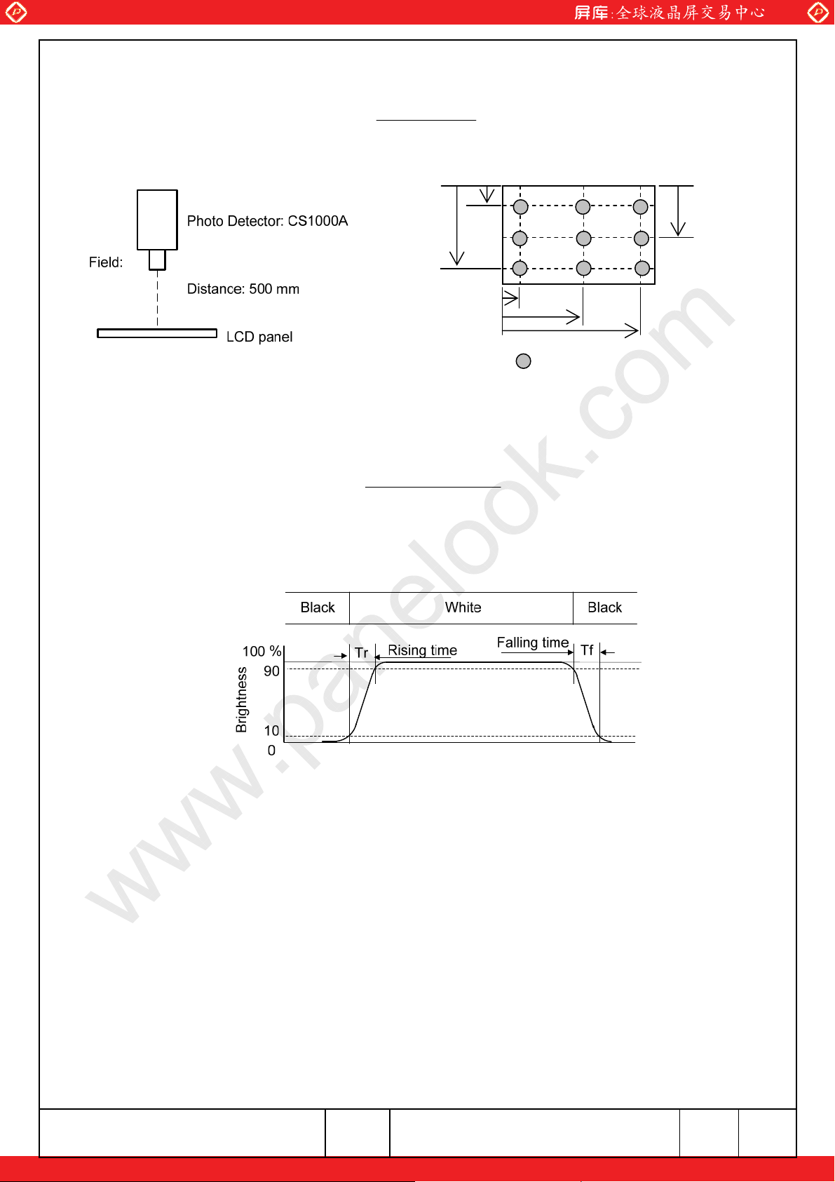
Note 3: The brightness uniformity is calculated by the equation as below:
uniformityBrightness u
BrightnessMin.
BrightnessMax.
100%
, which is based on the brightness values of the 9 points measured by CS-1000A as shown in Fig. 6.2.
123
90%
$
1
10%
789
10%
烉measuring points
Fig. 6.1 Fig. 6.2
654
50%
50%
90%
Note 4: The Contrast Ratio is measured from the center point of the panel, P5, and defined as the
following equation:
CR
WhiteofBrightness
BlackofBrightness
Note 5: The definition of response time is shown in Fig. 6.3. The rising time is the period from 10%
brightness to 90% brightness when the data is from black to white. Oppositely, Falling time is
the period from 90% brightness rising to 10% brightness.
Fig 6.3
Note 6: The color chromaticity is measured from the center point of the panel, P5, as shown in Fig. 6.2.
KAOHSIUNG OPTO-ELECTRONICS INC.
SHEET
NO.
7B64PS 2706-TX43D50VM0BAA-1
One step solution for LCD / PDP / OLED panel application: Datasheet, inventory and accessory!
PAGE 6-2/2
www.panelook.com
Page 10
Global LCD Panel Exchange Center
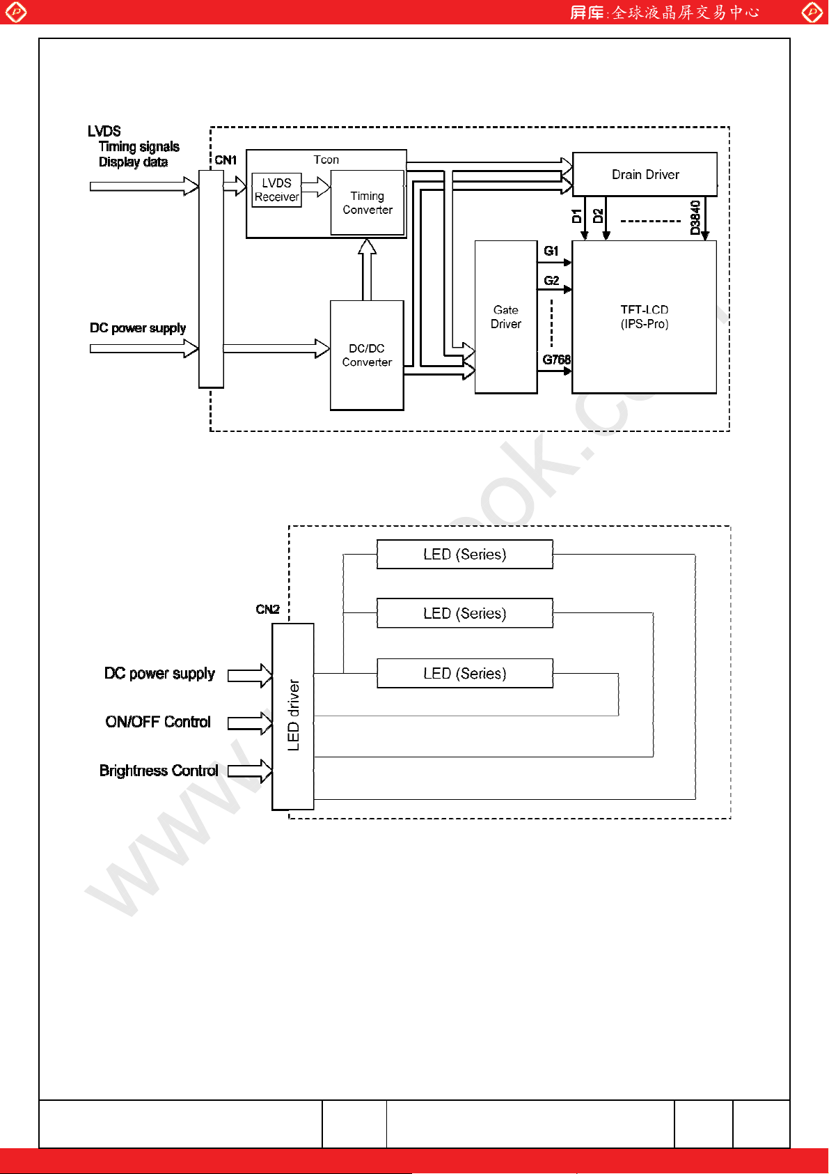
7. BLOCK DIAGRAM
7.1 TFT Module
www.panelook.com
7.2 Back light unit
KAOHSIUNG OPTO-ELECTRONICS INC.
One step solution for LCD / PDP / OLED panel application: Datasheet, inventory and accessory!
SHEET
NO.
7B64PS 2707-TX43D50VM0BAA-1
PAGE 7-1/1
www.panelook.com
Page 11
Global LCD Panel Exchange Center
www.panelook.com
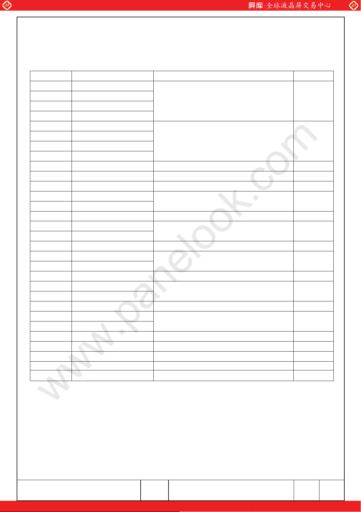
8. INTERFACE PIN ASSIGNMENT
8.1 TFT-LCD MODULE
CN1: JAE: FI-X30SSLA-HF or Equivalent
(Matching connector: JAE: FI-X30HL or FI-X30C2L-NPB or Equivalent)
Pin No. Symbol
1 VDD
2 VDD
3 VDD
4 VDD
5
6
7
8
9 TEST1 Test Pin (OPEN) 3)
10 TEST2 Test Pin (OPEN)
11 VSS GND (0V) 1)
12 RX0-
13 RX0+
14 VSS GND (0V)
15 RX1-
16 RX1+
17 VSS GND (0V)
18 RX2-
19 RX2+
20 VSS GND (0V)
21 CLK-
22 CLK+
23 VSS GND (0V)
24 RX3-
25 RX3+
26 VSS
27 AMODE LVDS Mode Select
28 TEST3 Test Pin (OPEN)
29 TEST4 Test Pin (OPEN) 3)
30 VSS GND (0V) 1)
VSS
VSS
VSS
VSS
Power Supply (+5.0V)
GND (0V) 1)
Pixel Data
Pixel Data
Pixel Data
Pixel Clock
Pixel Data 2)
GND (0V) 1)
Function Note
4
3)
2)
1)
2)
1)
2)
1)
2)
1)
5)
3)
Notes 1) All Vss pins should be grounded.
2) RXn- and RXn+ (n=0,1,2,3), CLK- and CLK+ should be wired by twist-pairs
or side-by-side FPC patterns, respectively.
3) Please keep open.
4) All VDD pins should be connected to +50 V (typ.).
5) Please refer to page 8-4/5 "LVDS interface" for LVDS data mapping.
KAOHSIUNG OPTO-ELECTRONICS INC.
SHEET
NO.
7B64PS 2708-TX43D50VM0BAA-1
One step solution for LCD / PDP / OLED panel application: Datasheet, inventory and accessory!
PAGE 8-1/5
www.panelook.com
Page 12
Global LCD Panel Exchange Center
www.panelook.com
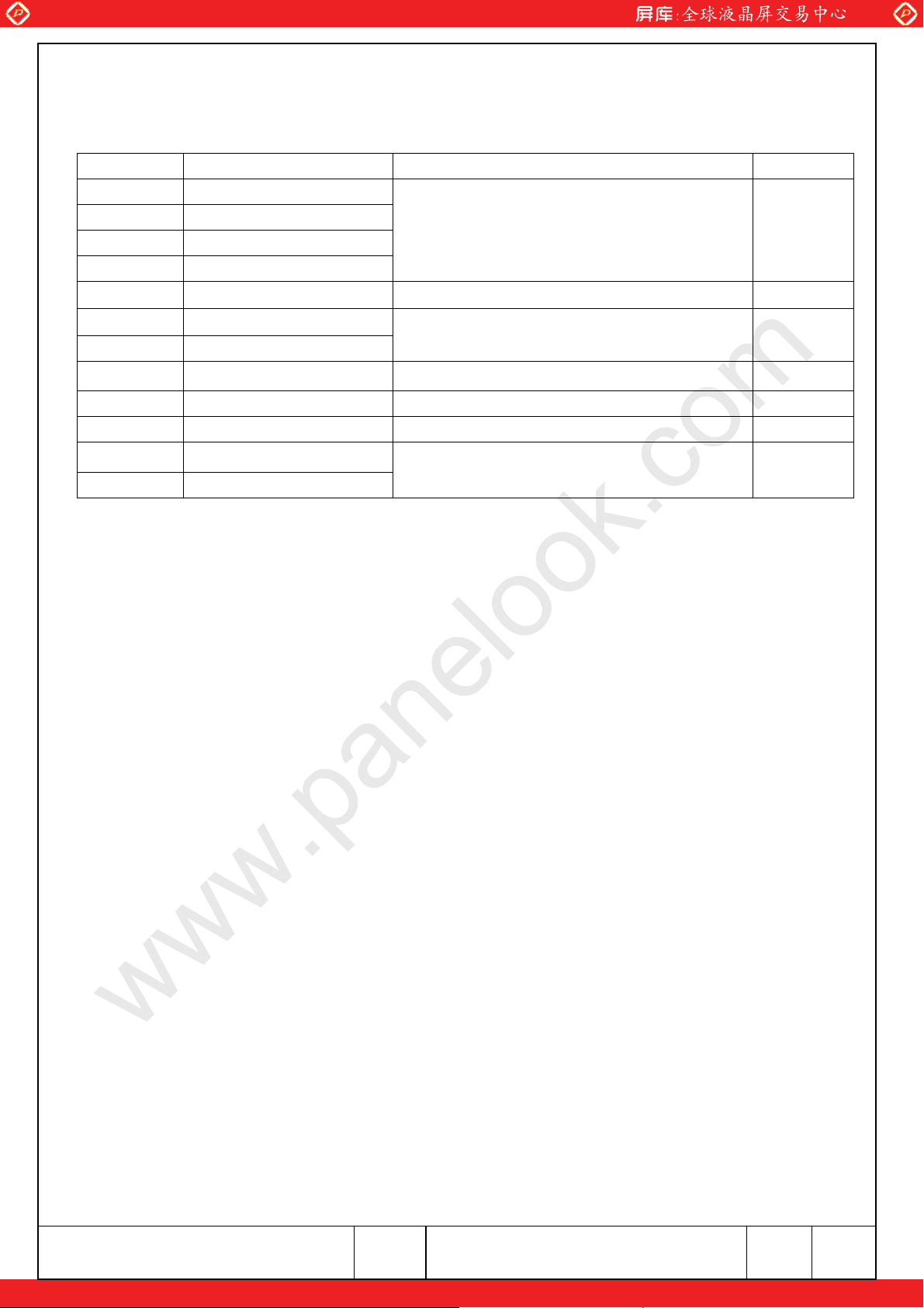
8.2 BACK-LIGHT UNIT
CN2 : TARNG YU Enterprise: TU2001WNR-12S
(Matching connector : JST PHR-12 or TARNG YU Enterprise TU2001HNO-12)
Pin No. Symbol Description Note
1 V
2 V
3 V
4 V
5 ON/OFF High : Backlight ON, Low : Backlight OFF 4)
IN
IN
IN
IN
Power Supply (typ. 12.0V) 1)
6 V
7 V
SS
SS
GND (0V) 2)
8 VBC Brightness Control Signal 5),6)
9 PWM PWM Dimming Signal 3),6)
10 NC NC -
11 V
12 V
SS
SS
GND (0V) 2)
Notes
1) All V
2) All V
pins should be connected to +12.0V (Typ.).
IN
pins should be grounded. The metal bezel is internally connected to GND.
SS
3) High level:2.5~5.0V, Low level:0~0.9
4) High level:2.5 ~ 5.0V DC, Low level:0 ~ 0.5V DC
5) Input Voltage : 1.0 ~ 3.6V DC
6) These signals can’t input at the same time.
KAOHSIUNG OPTO-ELECTRONICS INC.
SHEET
NO.
7B64PS 2708-TX43D50VM0BAA-1
One step solution for LCD / PDP / OLED panel application: Datasheet, inventory and accessory!
PAGE 8-2/5
www.panelook.com
Page 13
Global LCD Panel Exchange Center
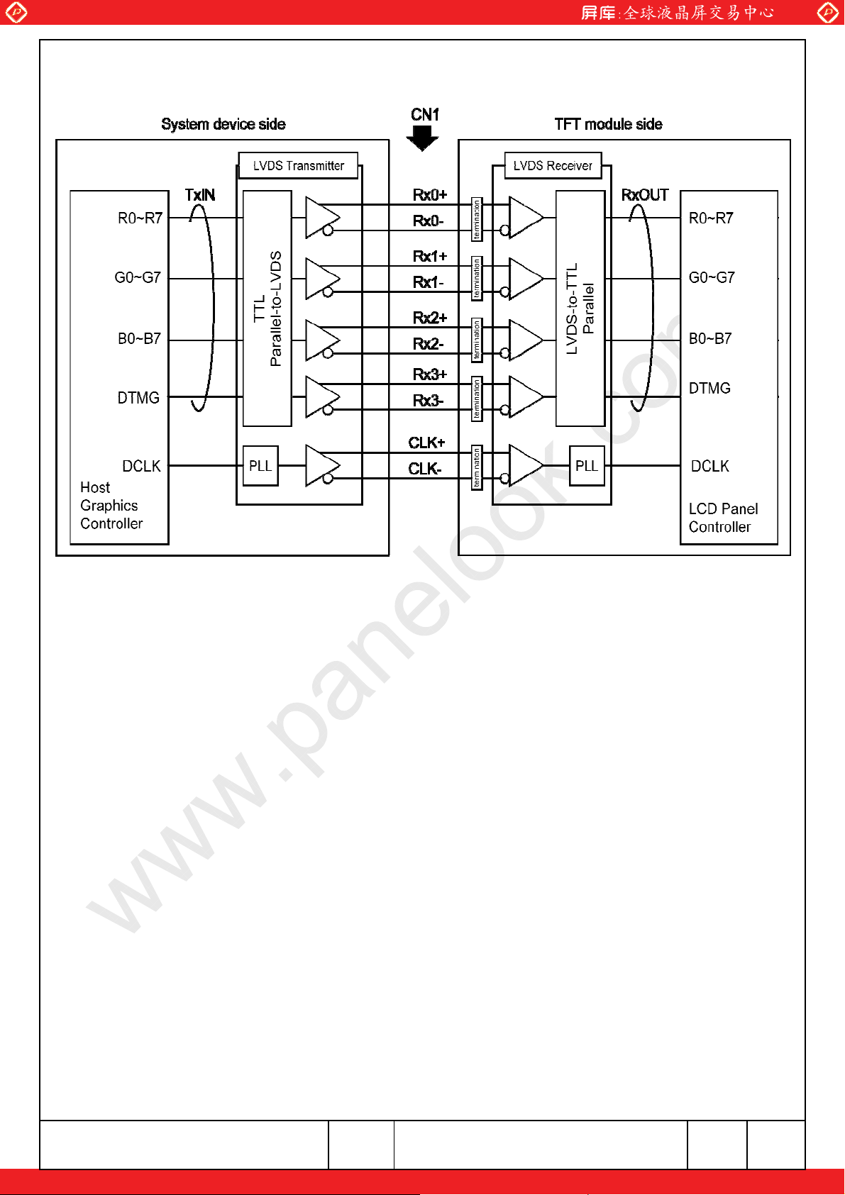
8.3 BLOCK DIAGRAM OF INTERFACE
www.panelook.com
Receiver: Equivalent of THC63LVDF84B by THine
R0~7 烉R data
G0~7
B0~7
DTMG
烉G data
烉B data
烉Display timing data
Notes 1) The system must have a LVDS transmitter to drive a module.
2) The impedance of LVDS cable shall be about 100 ohms per twist-pair line
when it is used differentially.
KAOHSIUNG OPTO-ELECTRONICS INC.
SHEET
NO.
7B64PS 2708-TX43D50VM0BAA-1
One step solution for LCD / PDP / OLED panel application: Datasheet, inventory and accessory!
PAGE 8-3/5
www.panelook.com
Page 14
Global LCD Panel Exchange Center
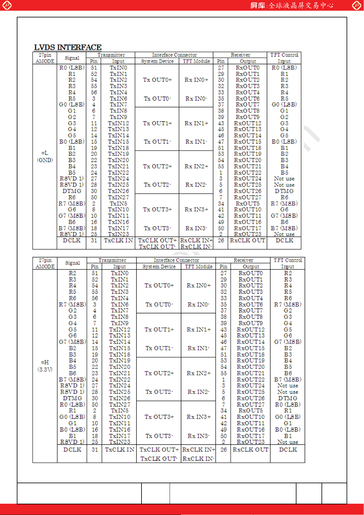
8.4 LVDS INTERFACE
www.panelook.com
Note 1) RSVD (reserved) pins on the transmitter shall be "H" or "L".
KAOHSIUNG OPTO-ELECTRONICS INC.
SHEET
NO.
7B64PS 2708-TX43D50VM0BAA-1
One step solution for LCD / PDP / OLED panel application: Datasheet, inventory and accessory!
PAGE 8-4/5
www.panelook.com
Page 15
Global LCD Panel Exchange Center
www.panelook.com
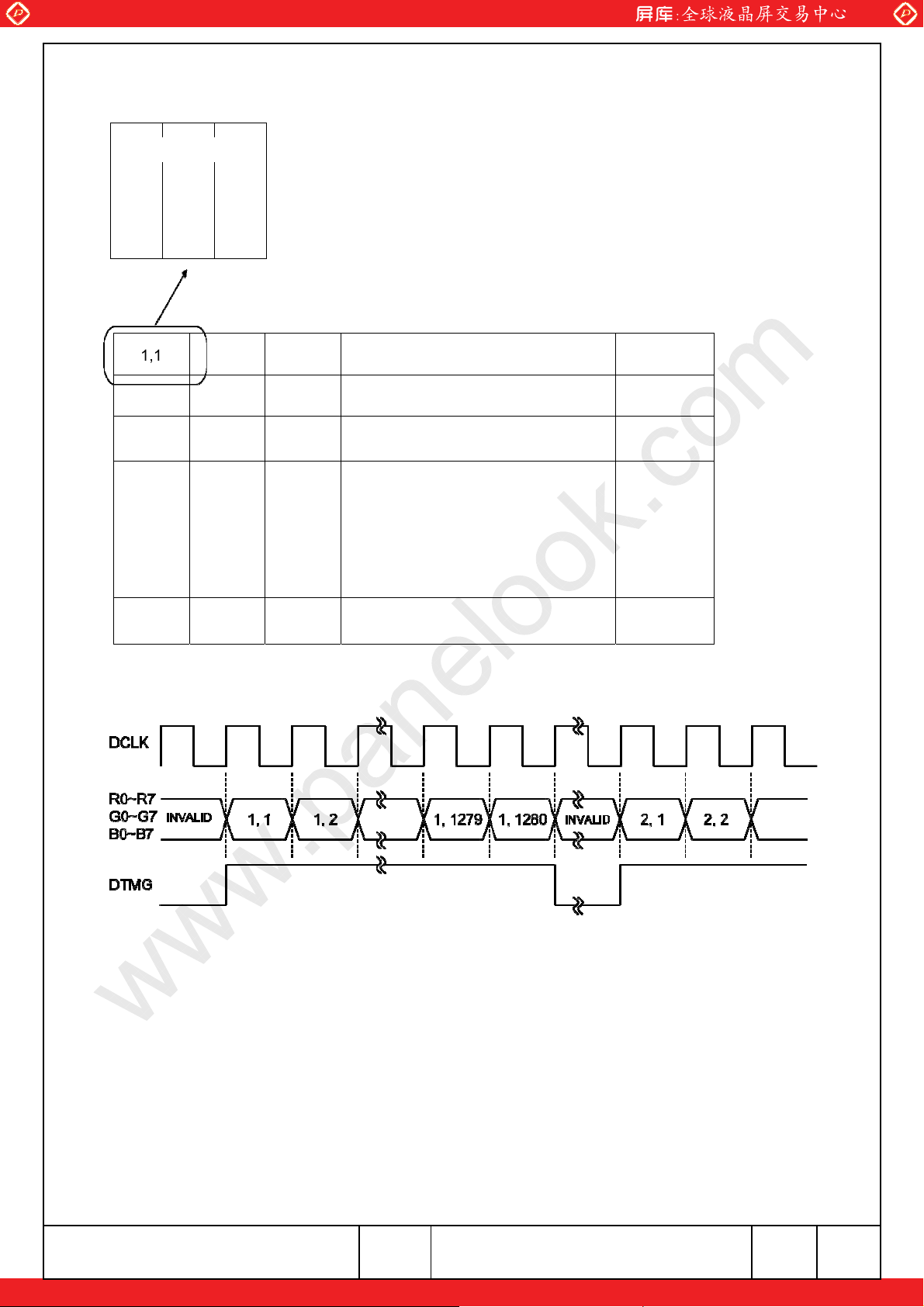
8.5 CORRESPONDENCE BETWEEN INPUT DATA AND DISPLAY IMAGE
R0~R7烉R data
(1,1)
RGB
1,1 1,2 1,3 ɃɃɃɃɃɃɃɃɃɃɃɃ 1,1280
2,1 2,2 2,3 ɃɃɃɃɃɃɃɃɃɃɃɃ 2,1280
3,1 3,2 3,3 ɃɃɃɃɃɃɃɃɃɃɃɃ 3,1280
G0~G7烉G data
B0~B7烉B data
ɃɃɃɃɃɃɃ
768,1 768,2 768,3 ɃɃɃɃɃɃɃɃɃɃɃɃ 768,1280
ɃɃɃɃɃɃɃ
ɃɃɃɃɃɃɃ
ɃɃɃɃɃɃɃ
KAOHSIUNG OPTO-ELECTRONICS INC.
SHEET
NO.
7B64PS 2708-TX43D50VM0BAA-1
One step solution for LCD / PDP / OLED panel application: Datasheet, inventory and accessory!
PAGE 8-5/5
www.panelook.com
Page 16
Global LCD Panel Exchange Center
炼
為
炼
炼
為
炼
為
炼
為
炼
為
炼
為
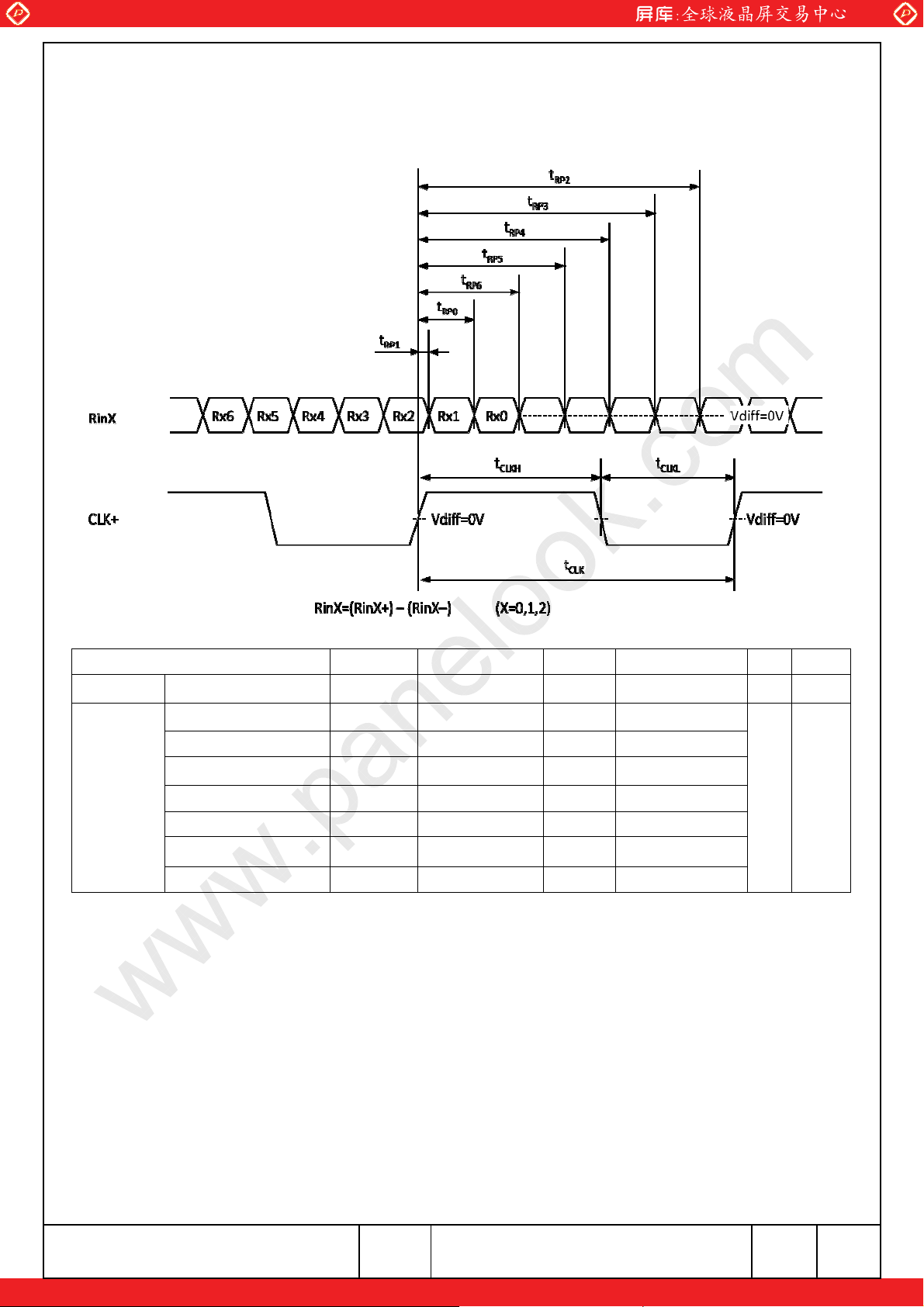
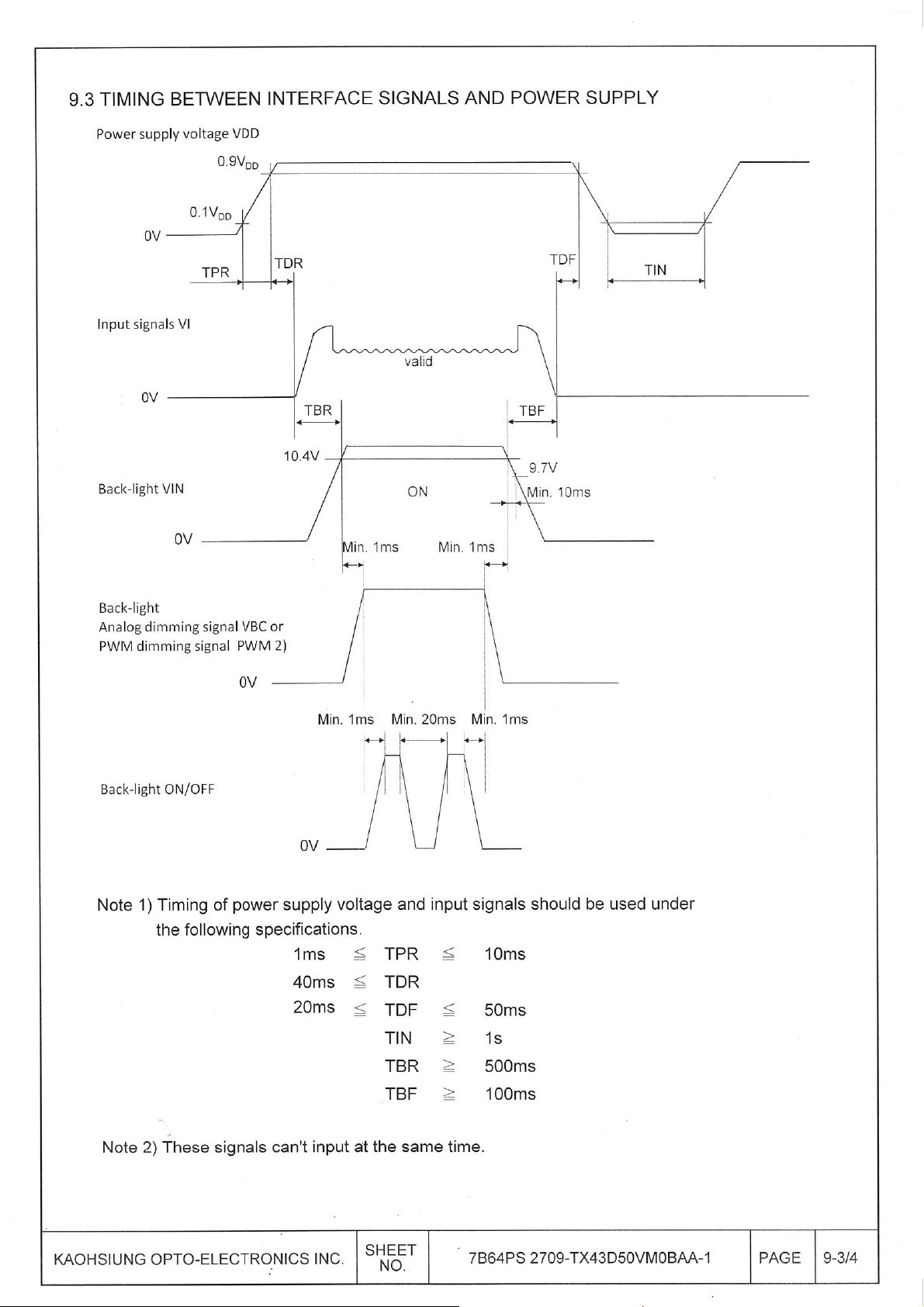
9. TIMING CHART
9.1 RECEIVER INPUT DATA POSITION
(Interface of TFT module)
www.panelook.com
Item Symbol Min. Typ. Max. Unit Note
DCLK Frequency 1/t
0 data position t
1st data position t
2nd data position t
RinX
(X=0,1,2)
3rd data position t
4th data position t
5th data position t
6th data position t
65 66 73 MHz
CLK
1/7t
RP0
RP1
6/7t
RP2
5/7t
RP3
4/7t
RP4
3/7t
RP5
2/7t
RP6
0.44 1/7t
CLK
0.44 0 為0.44
0.44 6/7t
CLK
0.44 5/7t
CLK
0.44 4/7t
CLK
0.44 3/7t
CLK
0.44 2/7t
CLK
CLK
CLK
CLK
CLK
CLK
CLK
1/7t
6/7t
5/7t
4/7t
3/7t
2/7t
CLK
CLK
CLK
CLK
CLK
CLK
0.44
0.44
0.44
0.44
0.44
0.44
ns
KAOHSIUNG OPTO-ELECTRONICS INC.
SHEET
NO.
7B64PS 2709-TX43D50VM0BAA-1
One step solution for LCD / PDP / OLED panel application: Datasheet, inventory and accessory!
PAGE 9-1/4
www.panelook.com
Page 17
Global LCD Panel Exchange Center
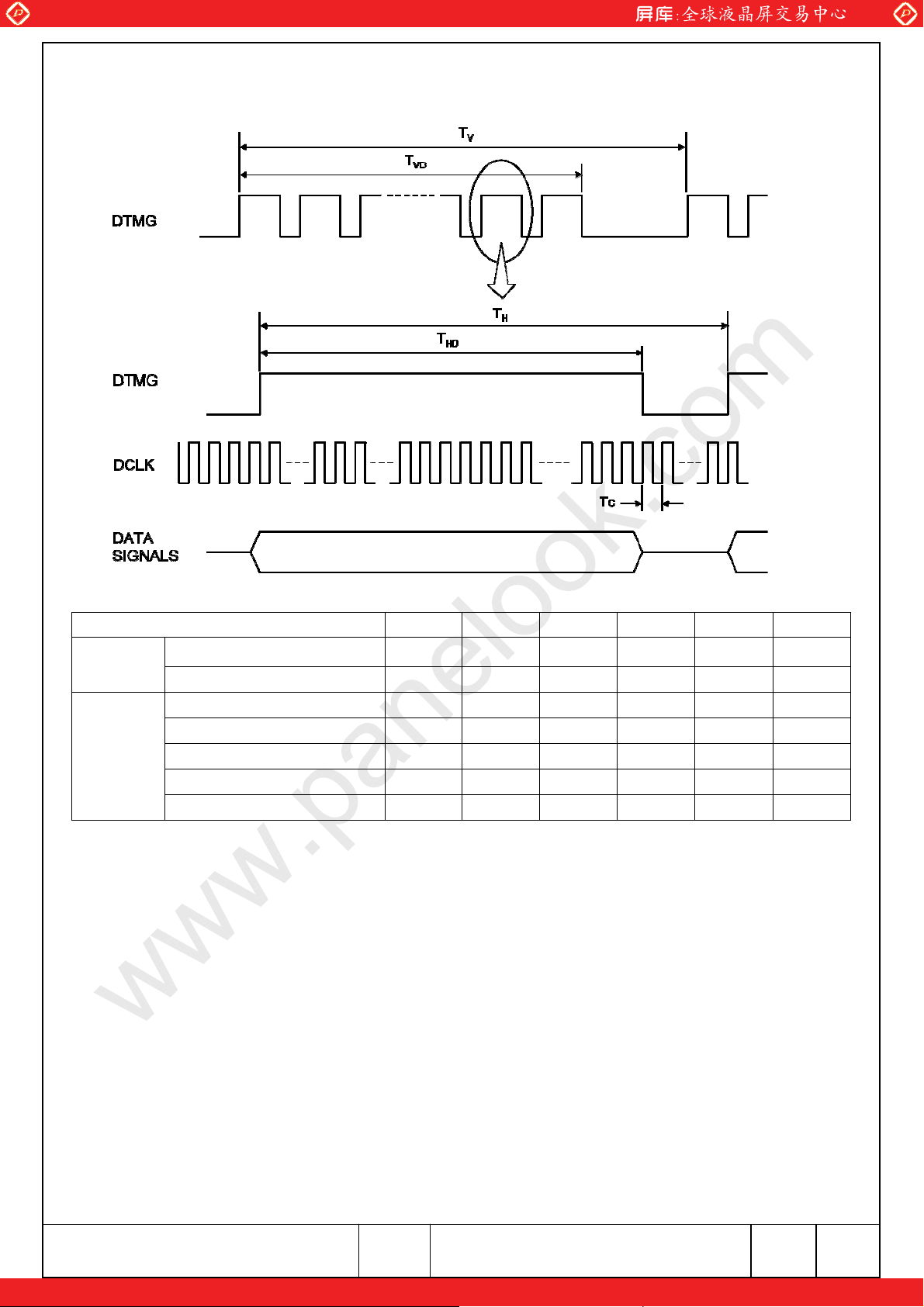
9.2 TIMING COVERTER SIGNAL TIMING
www.panelook.com
DCLK
DTMG
Item Symbol Min. Typ. Max. Unit Note
Cycle time t
13.7 15.1 15.4 ns
CLK
Duty D 0.35 0.5 0.65 -
Horizontal period T
Horizontal width-Active THD 1280 1280 1280 t
Vertical period TV 773 783 825 T
Vertical width-Active TVD 768 768 768 T
1396 1406 1450 t
H
CLK
CLK
H
H
Frame frequency fV 55 60 65 Hz
KAOHSIUNG OPTO-ELECTRONICS INC.
SHEET
NO.
7B64PS 2709-TX43D50VM0BAA-1
One step solution for LCD / PDP / OLED panel application: Datasheet, inventory and accessory!
PAGE
9-2/4
www.panelook.com
Page 18
Global LCD Panel Exchange Center
www.panelook.com
One step solution for LCD / PDP / OLED panel application: Datasheet, inventory and accessory!
www.panelook.com
Page 19

Global LCD Panel Exchange Center
www.panelook.com
9.4 DATA INPUT for DISPLAY COLOR
Input data R data G data B data
R3
Color MSB LSB MSB LSB MSB LSB
Basic
Color
Red
Black
Red (255)
Green (255)
Blue (255)
Cyan
Magenta
Yellow
White
Black
Red (1)
Red (2)
……
0000 000 00000000 000
1111 110 00000000 0001
000 001 10111 1100
0
0000 000 01110000 1110
0000 001 11111 1 11
1111 110 01110000 111
11 111 10111 1 00
1111 111 11111111 1111
0000
0000 010 00000000 000
0000 100 0 00
…
…
…
…
…
…
000
0
0
0
1
1
0
0
0
…
…
……
R1 R0 G7R2 G6 G5 G4 G1 G0G2R7 R6 R5 R4 B4 B1 B0
0
1
0
0
0
1
1
1
000 00000 0 00
0
0
0
……
…
…
…
…
…
…
…
…
…
…
…
…
G3
0
0
1
0
1
1
0
0
1
1
11
00
00
00
…
…
…
…
…
…
B7 B6 B5
0000000 0
…
…
…
…
000
111
000
0
00
…
…
…
…
…
…
B3
B2
0
0
0
0
0
0
1
1
1
1
1
1
011
0
1
1
0
0
0
0
0
0
……
…
…
…
…
…
…
Green
Blue
Red (254)
Red (255)
Black
Green (1)
Green (2)
…… …
Green (254)
Green (255)
Black
Blue (1)
Blue (2)
…
Blue (254)
Blue (255)
11
1111 1100 000 000
0000 000 00000 0000
0000 000 10000 0000
0000 000 00000 100
…
…
00
0000 001 1000111 111 0 00
0000
0000 000 0000000 000 0 01
0000
…
…
00
0000 000
11 100 00 00 0
…
…
…
…
00 001
…
…
…
…
000
1
1
0
0
0
…
…
…
…
0
0
0
0
0
…
…
……
Notes 1) Definition of gray scale: Color (n)
n indicates gray scale level. Higher n means brighter level.
2) Data signals: 1: High, 0: Low
1
1
0
……
…
…
0
0
0
0
0
…
…
…
…
000
0
0
0
…
…
…
…
…
…
…
…
…
………
…
…
000000
…
…
…
………
………
000000
………
………
00
…
…
…
…
000 000
000
0000
0000
000
000
…
…
0000111 111 0
0
…
0
000
…
…
…
…
00
…
…
…
…
1
…
…
…
…
0
0
0
0
0
0
0
0
0
0
…
…
0000
……
1
1
…
……
…
0
0
0
0
0
0
0
0
0
0
…
……
…
1
1
1
0
00
00
00
00
……
…
…
0
0
00
10
…
…
…
…
0
111000 000
1000101110
100 0
KAOHSIUNG OPTO-ELECTRONICS INC.
SHEET
NO.
7B64PS 2709-TX43D50VM0BAA-1
One step solution for LCD / PDP / OLED panel application: Datasheet, inventory and accessory!
PAGE
9-4/4
www.panelook.com
Page 20
Global LCD Panel Exchange Center
www.panelook.com
Unit: mm
Scale:NTS
10-1/2
PAGE
7B64PS 2710-TX43D50VM0BAA-1
No.
SHEET
KAOHSIUNG OPTO-ELECTRONICS
Note
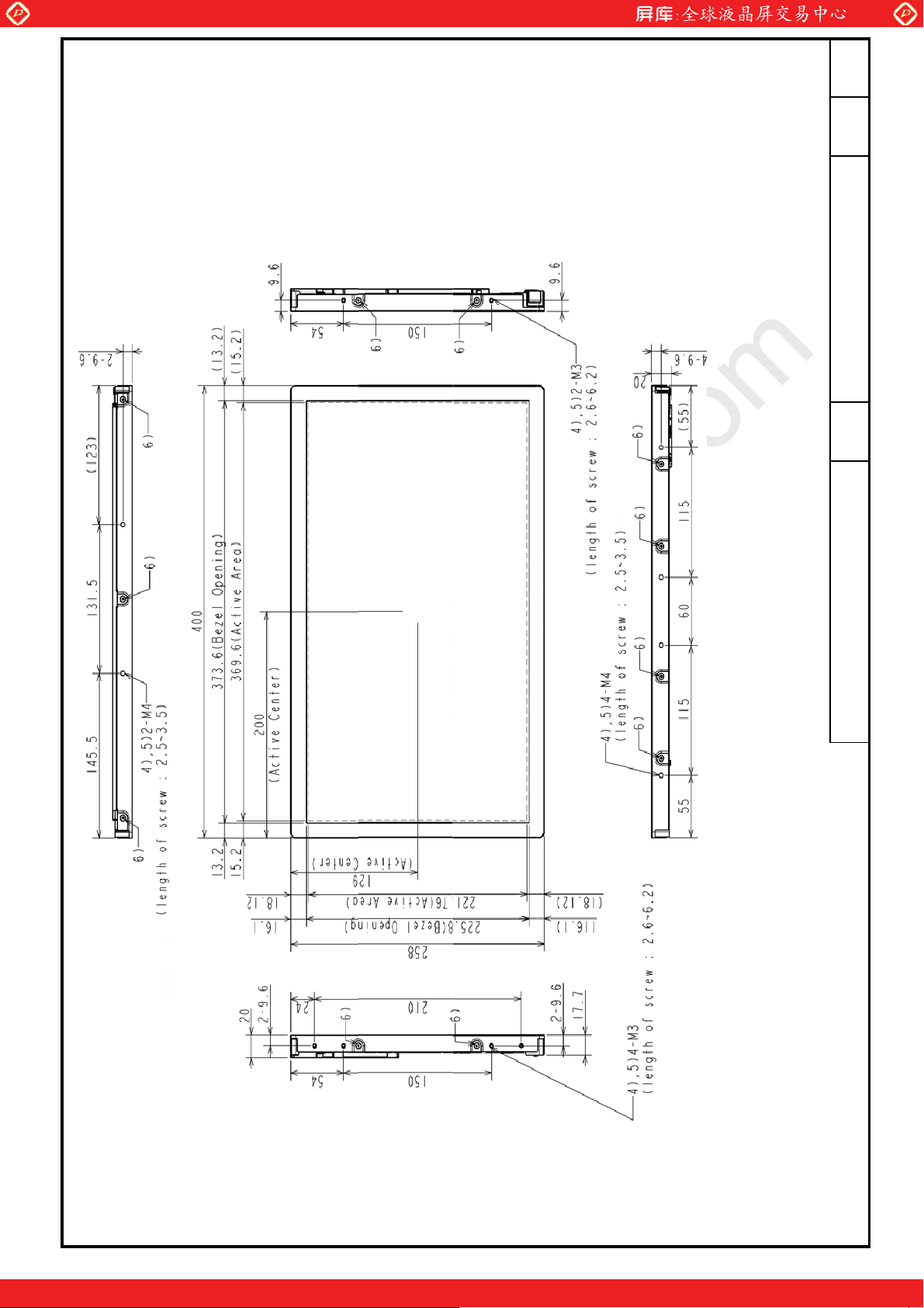
1) Interface connector (CN1)
JAE: FI-X30SSLA-HF or equivalent
10.1 FRONT VIEW
10. OUTLINE DIMENSIONS
One step solution for LCD / PDP / OLED panel application: Datasheet, inventory and accessory!
TARNG YU Enterprise: TU2001WNR-12S or equivalent.
6) Screws for panel fixation to the panel frame.
2) Converter PCB connector (CN2)
3) The unspecified tolerance: Ʋ0.5mm
4) Holes for panel mount : M3: 6 holes (right and left side), M4: 6 holes (upper and lower side)
7) Screws for LED bar fixation. (M3)
5) Maximum screwing torque for panel mount : 0.294Nίm (3kgfίcm)
www.panelook.com
Page 21
Global LCD Panel Exchange Center
www.panelook.com
10-2/2
Unit: mm
Scale:NTS
PAGE
7B64PS2710TX43D50VM0BAA1
No.
SHEET
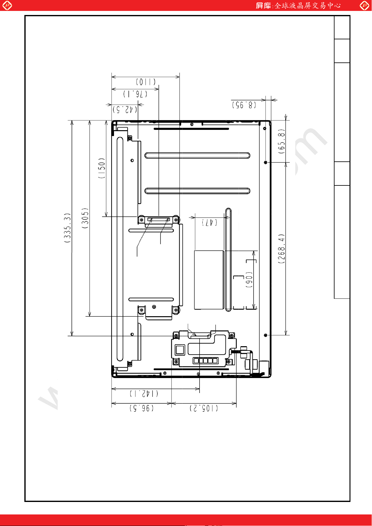
CN1
PIN1
CN2
LABEL
PIN1
KAOHSIUNG OPTO-ELECTRONICS
10.2 FRAR VIEW
One step solution for LCD / PDP / OLED panel application: Datasheet, inventory and accessory!
www.panelook.com
Page 22
Global LCD Panel Exchange Center
www.panelook.com
11. APPEARANCE STANDARD
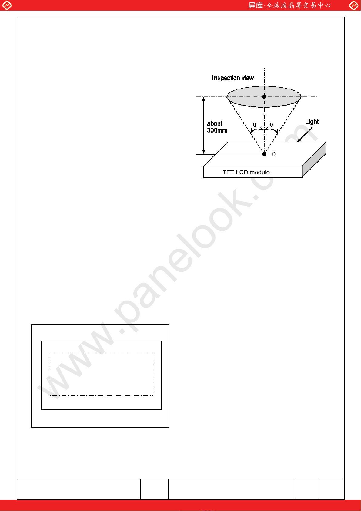
11.1 CONDITIONS FOR COSMETIC INSPECTION
(1) Viewing zone
a) The figure shows the correspondence
between eyes (of inspector) and
TFT-LCD module.
烋 45°
烋 5°
: when non-operating inspection
: when operating inspection
b) Inspection should be executed only from
front side and only A-zone.
Cosmetic of B-zone and C-zone are ignore.
(refer to 9.2 DEFINITION OF ZONE)
(2) Environmental
a) Temperature 烉 25°C
b) Ambient light 烉 about 700 lx and non-directive when operating inspection.
烉about 1000 lx and non-directive when non-operating inspection.
c) Back-light 烉when non-operating inspection, back-light should be off.
11.2 DEFINITION OF ZONE
A-zone
B-zone
C-zone
A-zone 烉 Display area (pixel area).
B-zone 烉 Area between A-zone and C-zone.
C-zone 烉 Metal bezel area.
(Include I/F connector)
KAOHSIUNG OPTO-ELECTRONICS INC.
One step solution for LCD / PDP / OLED panel application: Datasheet, inventory and accessory!
SHEET
NO.
7B64PS 2711-TX43D50VM0BAA-1
PAGE 11-1/3
www.panelook.com
Page 23
Global LCD Panel Exchange Center
www.panelook.com
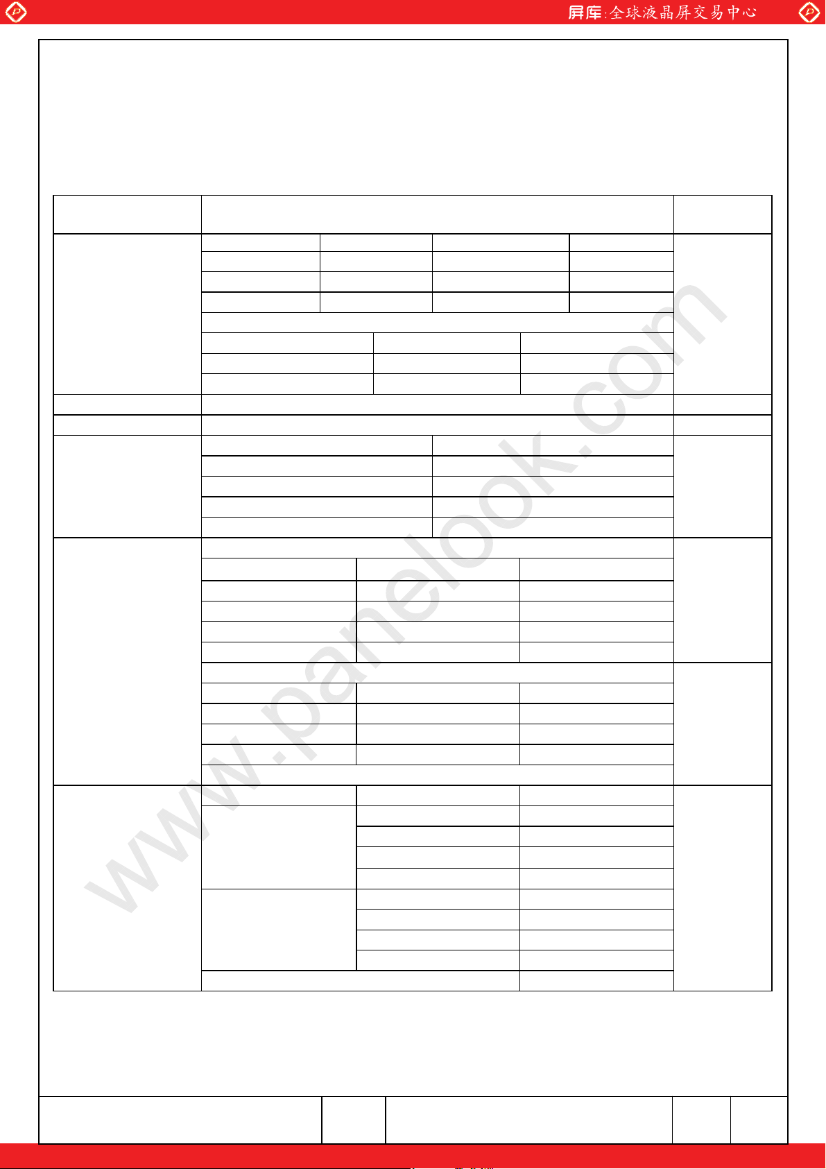
11.3 LCD APPEARANCE SPECIFICATION
The specification as below is defined as the amount of unexpected phenomenon or material in different
zones of LCD panel. The definitions of length, width and average diameter using in the table are shown
in Fig. 11.3 and Fig. 11.4.
Item Criteria Applied zone
Length (mm) Width (mm) Maximum number Minimum space
Ignored Wʀ0.02 Ignored -
Lʀ40 Wʀ0.04 10 -
Scratches
Dent Serious one is not allowed A
Wrinkles in polarizer Serious one is not allowed A
Bubbles on polarizer
1) Stains
2) Foreign Materials
3) Dark Spot
Dot-Defect
(Note 1)
Lʀ20 Wʀ0.08 10 -
Round (Dot Shape)
Average diameter (mm) Maximum number Minimum space
Dʀ0.2 Ignore Dʀ0.6 10 -
Average diameter (mm) Maximum number
Dʀ0.3 Ignored
0.3烋Dʀ0.5 10
0.5烋Dʀ1.0 5
1.0烋D none
Filamentous (Line shape)
Length (mm) Width (mm) Maximum number
- Wʀ0.02 Ignored
Lʀ4.0 Wʀ0.04 8
Lʀ2.0 Wʀ0.08 8
- W烍0.08 Dot Shape
Round (Dot shape)
Average diameter (mm) Maximum number -
Dʀ0.22 Ignored -
Dʀ0.5 8 D烍0.5 None -
Those wiped out easily are acceptable
Type Maximum number
1 dot 6
Bright dot-defect
Dark dot-defect
In total 15
2 adjacent dot 3
3 adjacent dot or above Not allowed
In total 6
1 dot 9
2 adjacent dot 5
3 adjacent dot or above Not allowed
In total 9
A,B
A
A,B
A,B
A
KAOHSIUNG OPTO-ELECTRONICS INC.
SHEET
NO.
7B64PS 2711-TX43D50VM0BAA-1
One step solution for LCD / PDP / OLED panel application: Datasheet, inventory and accessory!
PAGE
11-2/3
www.panelook.com
Page 24
Global LCD Panel Exchange Center
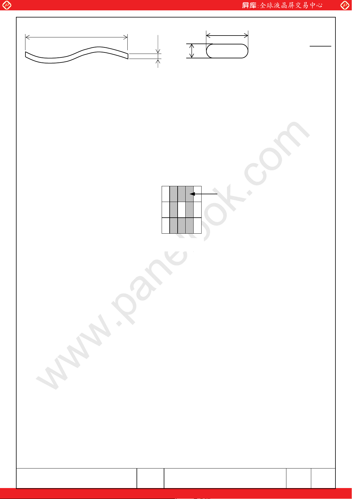
Length
Fig 11.3
Note 1: The definitions of dot defect are as below:
- The defect area of the dot must be bigger than half of a dot.
- For bright dot-defect, showing black pattern, the dot’s brightness must be over 30% brighter
than others.
- For dark dot-defect, showing white pattern, the dot’s brightness must be under 70% darker
than others.
- The definition of 1-dot-defect is the defect-dot, which is isolated and no adjacent defect-dot.
- The definition of adjacent dot is shown as Fig. 11.5.
www.panelook.com
Width
b
a
Fig 11.4
Average diameter =
a+b
2
- The Density of dot defect is defined in the area within diameter
A
Fig. 12.5
Fig 11.5
Note 2: Polarizer area inside of B-Zone is not applied.
I =20mm.
The dots colored gray are
adjacent to defect-dot A.
KAOHSIUNG OPTO-ELECTRONICS INC.
One step solution for LCD / PDP / OLED panel application: Datasheet, inventory and accessory!
SHEET
NO.
7B64PS 2711-TX43D50VM0BAA-1
PAGE
11-3/3
www.panelook.com
Page 25
Global LCD Panel Exchange Center
www.panelook.com
12. PRECAUTIONS
12.1 PRECAUTIONS of ESD
1) Before handling the display, please ensure your body has been connected to ground to avoid any
damages by ESD. Also, do not touch display’s interface directly when assembling.
2) Please remove the protection film very slowly before turning on the display to avoid generating ESD.
12.2 PRECAUTIONS of HANDLING
1) In order to keep the appearance of display in good condition, please do not rub any surfaces of the
displays by sharp tools harder than 3H, especially touch panel, metal frame and polarizer.
2) Please do not pile the displays in order to avoid any scars leaving on the display. In order to avoid
any injuries, please pay more attention for the edges of glasses and metal frame, and wear finger
cots to protect yourself and the display before working on it.
3) Touching the display area or the terminal pins with bare hand is prohibited. This is because it will
stain the display area and cause poor insulation between terminal pins, and might affect display’s
electrical characteristics furthermore.
4) Do not use any harmful chemicals such as acetone, toluene, and isopropyl alcohol to clean display’s
surfaces.
5) Please use soft cloth or absorbent cotton with ethanol to clean the display by gently wiping.
Moreover, when wiping the display, please wipe it by horizontal or vertical direction instead of
circling to prevent leaving scars on the display’s surface, especially polarizer.
6) Please wipe any unknown liquids immediately such as saliva, water or dew on the display to avoid
color fading or any permanently damages.
4
10 x 1,96
7) Maximum pressure to the surface of the display must be less than
adding pressure is less than 1
2
cm
, the maximum pressure must be less than 1.96N.
Pa. If the area of
12.3 PRECAUTIONS OF OPERATING
1) Please input signals and voltages to the displays according to the values defined in the section of
electrical characteristics to obtain the best performance. Any voltages over than absolute maximum
rating will cause permanent damages to this display. Also, any timing of the signals out of this
specification would cause unexpected performance.
2) When the display is operating at significant low temperature, the response time will be slower than it
at 25
However, these are temperature-related phenomenon of LCD and it will not cause permanent
damages to the display when used within the operating temperature.
$
C
. In high temperature, the color will be slightly dark and blue compared to original pattern.
3) The use of screen saver or sleep mode is recommended when static images are likely for long
periods of time. This is to avoid the possibility of image sticking.
4) Spike noise can cause malfunction of the circuit. The recommended limitation of spike noise is no
r
bigger than
KAOHSIUNG OPTO-ELECTRONICS INC.
One step solution for LCD / PDP / OLED panel application: Datasheet, inventory and accessory!
100 mV.
SHEET
NO.
7B64PS 2712-TX43D50VM0BAA-1
PAGE 12-1/2
www.panelook.com
Page 26
Global LCD Panel Exchange Center
www.panelook.com
12.4 PRECAUTIONS of STORAGE
If the displays are going to be stored for years, please be aware the following notices.
1) Please store the displays in a dark room to avoid any damages from sunlight and other sources of
UV light.
2) The recommended long term storage temperature is between 10
$
C
avoid causing bubbles between polarizer and LCD glasses, and polarizer peeling from LCD glasses.
3) It would be better to keep the displays in the container, which is shipped from KOE, and do not
unpack it.
4) Please do not stick any labels on the display surface for a long time, especially on the polarizer.
~35
$
and 55%~75% humidity to
C
KAOHSIUNG OPTO-ELECTRONICS INC.
One step solution for LCD / PDP / OLED panel application: Datasheet, inventory and accessory!
SHEET
NO.
7B64PS 2712-TX43D50VM0BAA-1
PAGE
12-2/2
www.panelook.com
Page 27

Global LCD Panel Exchange Center
www.panelook.com
13. DESIGN ATION OF LOT MARK
1) The lot mark is showing in Fig.13.3. First 4 digits are used to represent production lot, T represented
made in Taiwan, and the last 5 digits are the serial number.
2) The tables as below are showing what the first 4 digits of lot mark are shorted for.
8 0 3 5 T 0 2 0 3 0
Serial number
T : Made in Taiwan
Week
Month
Year
Year Mark
2012 2
2013 3
2014 4
2015 5
2016 6
Month Mark Month Mark
1 01 7 07
2 02 8 08
3 03 9 09
4 04 10 10
5 05 11 11
6 06 12 12
Week (Days) Mark
1~7 1
8~14 2
15~21 3
22~28 4
29~31 5
3) Except letters I and O, revision number will be shown on lot mark and following letters A to Z.
4) The location of the lot mark is on the back of the display shown in Fig. 13.3.
TX43D50VM0BAA
REV: A
2042T (5D) 123456
KOE MADE IN TAIWAN
Fig 13.3
KAOHSIUNG OPTO-ELECTRONICS INC.
One step solution for LCD / PDP / OLED panel application: Datasheet, inventory and accessory!
SHEET
NO.
7B64PS 2713-TX43D50VM0BAA-1
PAGE
13-1/1
www.panelook.com
 Loading...