

Page 1

CP2896TA
SERVICE MANUAL
VORSICHT:
Data contained within this Service
Verbesserungen
ä
ndern.
MANUEL D’ENTRETIEN
WARTUNGSHANDBUCH
CAUTION:
Before servicing this chassis, it is important that the service technician read
the “Safety Precautions” and “Product Safety Notices” in this service manual.
ATTENTION:
Avant d’effectuer l’entretien du châassis, le technicien doit lire les
«Précautions de sécurité» et les «Notices de sécurité du produit» présentés
dans le présent manuel.
No. 0103
CP2896TAN
CP2996TA
CP2996TAN
manual is subject to alteration for
improvement.
Les données fournies dans le
présent manuel d’entretien
peuvent faire l’objet de
modifications en vue de
perfectionner le produit.
Vor Öffnen des Gehäuses hat der Service-Ingenieur die „Sicherheitshinweise“
und „Hinweise zur Produktsicherheit“ in diesem Wartungshandbuch zu lesen.
TECHNICAL SPECIFICATIONS
TV System.............................PAL/SECAM B,G
NTSC 3.58/4.43 MHz via Scart
Mains voltage........................210..240 V, 50Hz
Power consumption................................135W
Standby power consumption...................0.2W
Picture tube
2896 TAN,2896 TA 71cm
2996 TAN,2996 TA 74cm
Sound output (RMS) ..................... 2 x 10W/8Ω
Connections
Front panel
Headphones 32..600Ω, 3.5mm
Audio/Video Audio in: 0..2V (RMS)
Video in: 1V/75Ω
Y/C in (SVHS)
Rear panel
A/V Audio in: 0..2V (RMS)
Audio out: 0..2V/10k (RMS)
Video in/out: 1V/75Ω
RGB in: 0.7V/75Ω (E1)
Y/C in: (SVHS)(E2)
Loudspeakers min 10W/8Ω (RMS)
Aerial 75Ω
Audio output 0..2V/10k (RCA)
SPÉCIFICATIONS TECHNIQUES
Systéme TV...........................PAL/SECAM B,G
NTSC 3.58/4.43 MHz via Scart
Tension secteur.....................210..240 V, 50Hz
Consommation .......................................135W
Consommation en veille...........................0.2W
Tube-image
2896 TAN,2896 TA 71cm
2996 TAN,2996 TA 74cm
Sortie sonore (RMS).........................2 x 10W/8
Connexions
Sur le panneau avant
Ecouteurs 32..600Ω, 3.5mm
Audio/vidéo Entrée audio:0..2V(RMS)
Entrée video: 1V/75Ω
Entrée Y/C: (SVHS)
Sur le panneau arrière
Audio/video Entrée audio:0..2V(RMS)
Sortie audio: 0..2V/10k (RMS)
Entrée vidéo/out: 1V/75Ω
Entrée RGB: 0.7V/75Ω (E1)
Entrée Y/C: (SVHS)(E2)
Haut-parleurs min 10W/8Ω (RMS)
Antenne 75Ω
Sortie audio 0..2V/10k (RCA)
Die in diesem Wartungshandbuch
enthaltenen Spezifikationen
können sich zwecks
TECHNICAL SPECIFICATIONS
TV-Norm................................PAL/SECAM B,G
NTSC 3.58/4.43 MHz via Scart
Netzspannung.......................210..240 V, 50Hz
Leistungsaufnahme.................................135W
Leistungsaufnahme im standby-modus...0.2W
Bildröhre
2896 TAN,2896 TA 71cm
2996 TAN,2996 TA 74cm
Tonleistung (RMS)......................... 2 x 10W/8Ω
Anschlüsse
An der Vorderseite
Kopfhörer 32..600Ω, 3.5mm
Audio/Video Audio ein: 0..2V (RMS)
Video ein: 1V/75Ω
Y/C ein (SVHS)
An der Rückseite
Audio/video Audio ein: 0..2V (RMS)
Audio aus: 0..2V/10k (RMS)
Video ein/aus: 1V/75Ω
RGB ein: 0.7V/75Ω (E1)
Y/C ein: (SVHS)(E2)
Lautsprecher min 10W/8Ω (RMS)
Antenne 75Ω
Audio-Ausgang 0..2V/10k (RCA)
December 1998
Page 2

2
Technical data
Technische Daten
Données téchniques
System
NTSC
Mains power
Consumption
1)
In stand-by
Frequency range
Sound output (RMS)
Subwoofer
2)
Connections on the front
panel
Headphones
Audio/Video
Connections on the rear
panel
Audio/Video
External loudspeakers
Antenna
Audio output
2)
Norm
NTSC
Netzanschluß
Leistungsaufnahme
Im Bereitschaft
Frequenzbereich
Tonendstufe (RMS)
Subwoofer
2)
Anschlüsse an der
Vorderseite
Kopfhöreranschluß
Audio/Video
Anschlüsse an der
Rückseite
Audio/Video
Externe Lautsprecher
Antennenanschluß
Audio Ausgang
2)
Systéme
NTSC
1)
Alimentation
Consommation
1)
En mode veille
Gamme de fréquences
Sortie sonore (RMS)
Subwoofer
2)
PAL/SECAM B, G
3.58/4.43 MHz via Scart
210...240 V, 50 Hz
135 W (normal)
0.2 W
48.25 - 855.25
2 x 10 W/8 Ω
14 W/16 Ω
Connexions sur le
panneau avant
Ecouteurs
Audio/Vidéo
32...600 Ω , 3.5 mm
Audio in: 0...2 V (RMS)
Video in: 1 V/75 Ω
Y/C in (SVHS)
Connexions sur le
panneau arrière
Audio/Vidéo
Audio in: 0...2 V (RMS)
Audio out: 0...2 V/10 kΩ
(RMS)
Video in/out: 1 V/75Ω
RGB in: 0.7 V/75Ω (E1)
Y/C in (SVHS) (E2)
Haut-parleurs externes
Antenne
Sortie audio
2)
min 10 W/8 Ω (RMS)
75 Ω
0...2 V/10 kΩ (RCA)
Specifications are subject
to change.
1)
Depends on option
modules and picture tube.
2)
Not in all models.
Änderungen vorbehalten
1)
Abhängig von
Optionsmodulen und
Bildröhre.
2)
Nicht in allen Modellen.
Les Spécifications
peuvent êt re modifiées
sans préavis.
1)
Dépend des modules
option-nels et du tube
cathodique.
2)
Pas sur tous les modèles.
Page 3
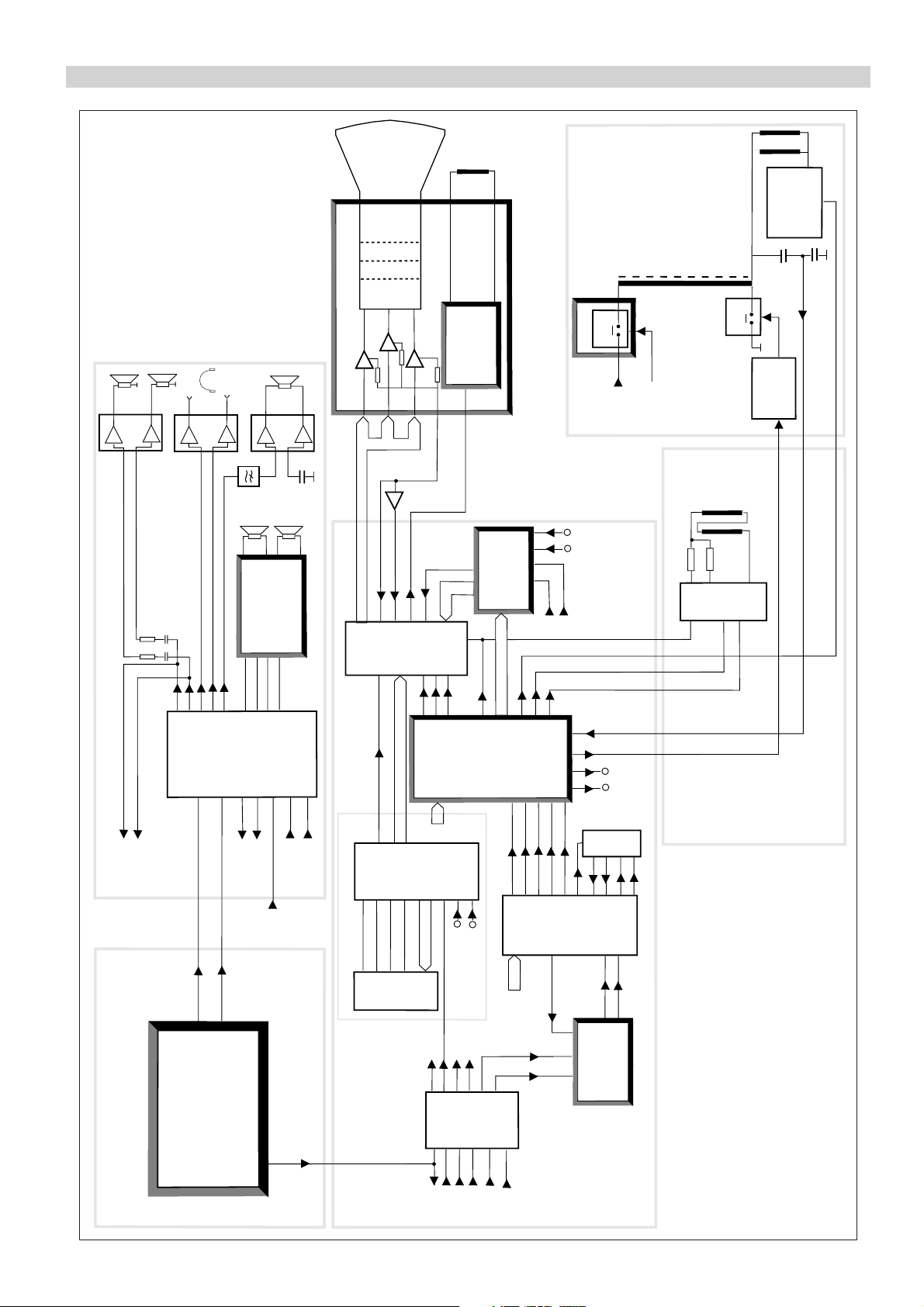
15
20, 22, 24
19
10-12
13
fb
2-4
1
fb
bcl
BC
8
6
7
ICt1
ICr2
44-46
18-27
ICr1
47
BLAN
141312
Y
ICd1
25
26
V
U
ICd3
423
1
RGB + fb
1718161514
C
CVBS/Y
C
ICq1
OUT
OUT
13
3
11
IN
IN
CVBS/Y
5, 6
IN
8, 10
IN
2H
2V
14
sc
17
11
HA
VA
10
SSc
D1D0D2
D3
32
33
34
35
I/O2
I/O1
I/O3
I/O4
2
1
24
25
9
CVBS
3
2V
4
2H
A0-A9
RGB
ICs1
Mk1
DATA IN
DATA OUT
WS
L
R
CL
L, R
L, R
L, R
AM
SIF
R, L
R, L
L
R
3D/Pro Logic
module
AR7xx
4
6
1
7
ICa1
29
28
26
25
9
1
ICa2
2
6
33, 34
36, 37
46, 47
49, 50
52, 53
55
60
141312
11
5
6
7
8
SOUND BLOCK
CRT module
HH7xx
ICh3
ICh2
ICh1
R
G
B
6
5
4
9
7
BC
SVM
module
VMxxx
PIP
module
PP7xx
RGB
RGB
IQTV2
&
DPLL
DB7xx
Flyback
EW
Ver
Ver
Hor
sc
111412
16
Comb filter
module
CF7xx
V
Y
U
11
10
67
13
15
14
18-21
Scart 1
3435333738
Camera
Scart 2
Scart 1
RF BLOCK
PIP
module
109
C
CVBS/Y
11 12
Scart 2
Scart 2
RGB
2H
2V
27 26
24
TELETEXT
VIDEO BLOCK
Adjustable
audio
Scart 1
Camera
Scart 3
VGA
Scart 2
Scart 1
17
Y
Tk3
SWxxx
U1
12V
22
17
20
19
18
12
11
1
9
2
Scart 1
26
Y
SVM coil
Diode
modulation
Dk7, Dk8
Tk4,ts1,ts2
5
Vertical
deflection
yoke
Horizontal
deflection
yoke
Line
driver
Tk1, Tk2
Vertical
deflection
and
E-W driver
Horizontal
deflection
5,9-12,14-18
MSP3410D
Audio
processor
TDA9143
Colour
decoder
TDA4780
RGB processor
SDA5275S
Megatext
514400
Text memory
TEA6417
Video switch
TDA8354
Vertical output
TDA2616
Audio power
amplifier
TL082
Headphone
amplifier
TV-Frontend
Tuner+IF
19
18
20
PIP
CVBS
1
Scart 3
IN
IN
23
1
Fsc
clock
VGA
VGA/RGB
5
6
4
ICa4
1
9
TDA2616
Active subwoofer
amplifier
ICa3
31
SUB
Block diagram, signal routes
3
Page 4
Scart-
buffers
TXT
ICr1
RAM
ICr2
Delay
ICd3
Deco/Sync
ICd1
RGB-proc.
ICt1
ROM
ICf1
NVM
ICf2
µP
ICf3
Video Switch
ICq1
HP-Ampl.
ICa3
Service
conn. &
buffer
Sound
processor
ICa2
Frontend
PIF SIF
TV-
Tuner
ICo6
Rec
ICo3
Rec
5V-r
12V-r
To4
Pict
12V-p
SVM module
CRT-module
8V-p
FEATURE BOX
32
30
8V-p
Comb-Filter
3
4
PIP-module
Decoder
ICp3
µP, ICp6
&
A/D, ICp5
13
12V-p
7V-fb
8V-p
12V-p
7
28
5
5V-r
Amplifiers
Digital Sound
Processor
5V-r
12
1
28V
ICo4
12V-r
10V
5V-stb
Control module
IR-
receiver
8
10
6
12V-p
5V-stb
Loudspeaker
Amplifier
ICa1
PP7xx
Rq48
AR7xx
FC7xx
CF7xx
20
22
23
24
15
17
18
14
21
19
3
4
ICo2
3
2
11
5
ICo1
6
16
1
14
Ro8,
14
Do8
Co10
Do2
Do1
Do4
Do3
Ro4, 10
Ro15
Ro18, 19
21, 22
To1
Ro70
Co15
230V
50Hz
Ftc1
Fo1
Do12
Do11
Do9
Do13
U1
32
PWM
Line
sync.
Do17
Ro32
Fo3
Fo2
Do14
Do16
Ro42
Ro45
Ro50
Do20
8
2
5
!
!
Ro44, 46
ZDk1
7V
Mains non isolated
17V
7V-fb
Ro49
Ro48
!
Mo2
!
Mo3
!
Vert.deflection
& EW driver
ICs1
Mk1
Rk2
Dk1
8
10
11
12
1
7
Rk9
Dk2
Rk19
Dk3
6.3V RMS
30kV
500V
8 kV
Rk15
Rk45
200V
53V
Rk4
!
!
!
!
!
Tk3
Rk20
!
16V
SWxxx
Rk11, 12
13, 14
HH7xx
Line
driver
12V-p
12V-p
12V-p
!
7V
G2
Focus
Heater
5
4
3
6
12V-p
8V
Ra18
AUX
module
12V-p
TA700
And
ICf4
Reset
ICf5
Subwoofer
Amplifier
ICa4
I
2
C Switch
11
30V
2
30V
Rq54
Rq2
Tq5
8.5V
Rr18
Scart 3 module
TA710/711
4
10
Tuner
To15
To9
Cfc23
FC7xx
Control module
Start
ICfc1
ICfc2
2
1
47
14
Cfc24
Cfc26
Dfc11
Hfc2
3
Zdo1,To8
RGB
Switch
ICp7
I
2
C Switch
ttp5
IF
ICp1
Delay-line
ICp4
DB7xx
SR7xx
Cancellor
VMxxx
Defl. ctrl
IC17
Filters
5V
3V
IC1
DSP
IC4
IQTV
4
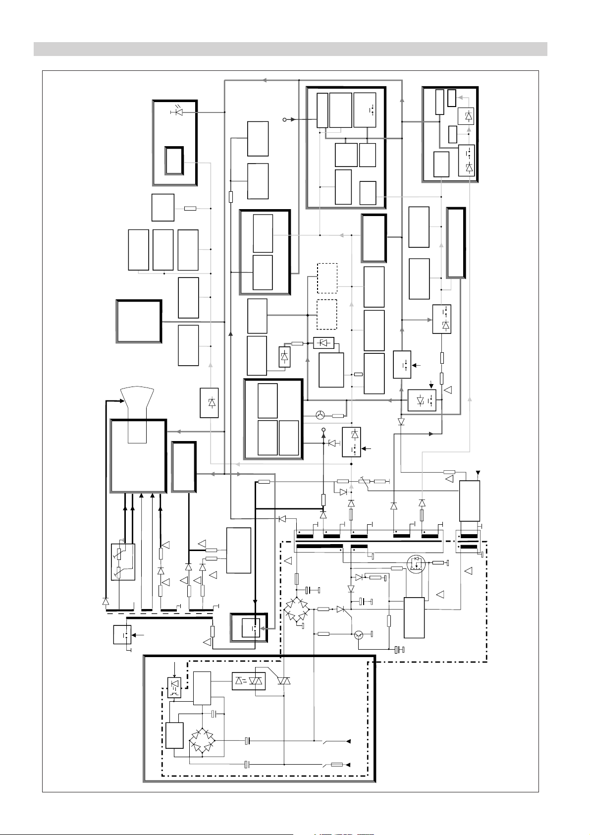
Block diagram, power supply
Page 5

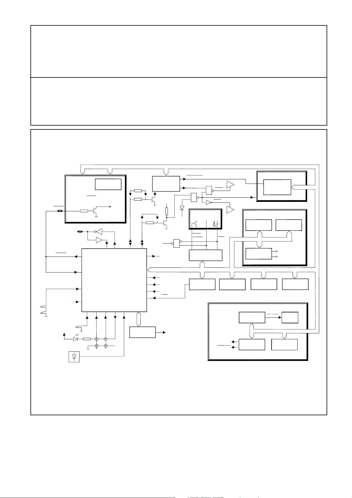
Block diagram, control signals
µP
ICf3
PIP-MODULE
FEATURE BOX DB7xx
Comb-Filter
module
TV tuner
SDA
SCL
+5V
Local control
HP ind
Rec / IR
IR Receiver
TXT
ICr1
M3L
Status 2
Status 1
Status 3
Hold
Surround
processor
ICar2
Sound
processor
ICa2
Deflection
IC 17
IQTV µP
IC 18
Deco/Sync
ICd1
Subwoofer
mute
5
MSP Reset
Bypass /
Comb-ID
NTSC
RGB processor
ICt1
Video Switch
ICq1
NVM
ICf2
PIP µP
ICp6
Deco/Sync
ICp3
Video switch
PIP/ext. RGB
Service
connector
545352
7
50
1
61 62
46
64
44, 45
4, 59, 60
AUDIO FEATURE BOX
17, 18
5, 6
8, 9
17, 18
5, 6 2, 4 27, 28
9, 10
49, 50, 51
51, 61
85
DPLL
IC 11
40, 41
9,10
24
40,41
3, 4
1, 2
3
PIP tuner
IF
ICp1
L-norm
15
16
37
38
VGA
1/2 FM
Bridges:
Mute
2
7
E3-control
(3-state)
&
APSi
test
Subwoofer
ident.
RGB
status
Line-out
status
6
3
FRONTEND
Multi: Strobe to write I/O-latch
Single: APSi control
IF ident.
resistor
APSi filter/Strobe
Strobe
APSi
(Single norm)
47
55
IF Ident.
15
16
23
13
2
1
5, 6
FSC /
SVHS
263
AV-link
PWM
Scart pin 10
16:9 ident.
51
12Vp
PA-mute
&
OR
28V
PA
PA
mute
mute
Subwoofer
Int-LS
15
4
I
2
C
I
2
C
DSP Reset
12V
4, 57, 8
10
A/D
Hor. shift
5
A/D
A/D
A/D
4, 5
8
8
ΤΑ700
8,9
Picture tilt
PWM
1
)
1
)
1
)
If no mux. and
picture tilt
mux.
ΤΑ710
Upict
Urec
U
49
48
Start
Rec-on
Pict-on
11 = Off
00 = TV
01 = Record
10 = Service
3
5
Page 6
MULTI CONCEPT
MX/MZ-CHASSIS
G Functional description
2
C
I
4, 57, 8
APSi filter/Strobe
Scart pin 10
Strobe
APSi
RGB status
FRONTEND
Multi: Strobe to write I/O-latch
Single: APSi control
(Single norm)
IF Ident.
Line-out
status
Rec / IR
IF ident.
resistor
47
55
3
6
HP ind
10
+5V
A/D
1
TV tuner
AV-link
µP
ICf3
61 62
Local control
263
46
64
Subwoofer
ident.
16:9 ident.
MSP Reset
50
PWM
SDA
SCL
A/D
A/D
A/D
M3L
4, 59, 60
49, 50, 51
TXT
ICr1
PA-mute
51
5
44, 45
54
53
52
7
Sound
processor
ICa2
24
12Vp
APSi
test
Hor. shift
Status 2
Status 1
Status 3
Hold
7
E3-control
9, 10
&
(3-state)
4
5
12V
28V
DSP Reset
Subwoofer
mute
&
Comb-Filter
module
13
Bypass /
Comb-ID
15
Deco/Sync
Service
3
connector
OR
mute
2
NTSC
16
ICd1
5, 6
1, 2
PIP-MODULE
Video switch
PIP/ext. RGB
mute
1
FSC /
SVHS
23
T V
1997
AUDIO FEATURE BOX
15
85
PA
Subwoofer
Mute
Int-LS
PA
FEATURE BOX DB7xx
Deflection
40,41
2
I
C
5, 6 2, 4 27, 28
NVM
ICf2
PIP tuner
16
Deco/Sync
15
ICp3
Surround
processor
2
IC 17
17, 18
40, 41
DPLL
IC 11
Video Switch
ICq1
L-norm
8
4, 5
5, 6
ICar2
37
38
Bridges:
1/2 FM
VGA
8
PIP µP
IQTV µP
IC 18
RGB processor
ICp1
ICp6
51, 61
IF
17, 18
9,10
8, 9
ICt1
3, 4
IR Receiver
6611 72 76
Page 7

Contents
MICROPOWER CONTROL.........................................................................................................................................................1
POWER SUPPLY ........................................................................................................................................................................ 2
RECEPTION ................................................................................................................................................................................4
AUDIO SECTION........................................................................................................................................................................5
Multistandard Sound Processor, ICa2................................................................................................................................ 5
Audio Power Amplifier, ICa1...............................................................................................................................................6
Headphone Amplifier, ICa3 .................................................................................................................................................6
VIDEO SECTION ........................................................................................................................................................................7
Video Matrix Switch, ICq1...................................................................................................................................................7
Colour Decoder / Sync Processor, ICd1 .............................................................................................................................7
Baseband Delay Line, ICd3 ................................................................................................................................................. 8
Feature boxes, DB7** .........................................................................................................................................................9
Feature box DB711 ..............................................................................................................................................................9
Analog to digital converter, ic9...........................................................................................................................................9
Field memory, ic14 ............................................................................................................................................................10
IQTV2 circuit, ic18 ..............................................................................................................................................................10
DPLL1 circuit, ic11 .............................................................................................................................................................11
Deflection Controller TDA9151, IC17 ...............................................................................................................................11
Feature box DB710 ............................................................................................................................................................ 12
Feature box DB700 ............................................................................................................................................................ 12
RGB Video Processor TDA4780, ICt1 ............................................................................................................................... 13
CRT module........................................................................................................................................................................14
Teletext ...............................................................................................................................................................................15
Megatext SDA5273, ICr1 ...................................................................................................................................................15
Megatext Plus SDA5275, ICr1 ...........................................................................................................................................15
Teletext memory DRAM, icr2 ............................................................................................................................................15
29
CONTROL SYSTEM ................................................................................................................................................................. 16
Program memory, ICf1...................................................................................................................................................... 16
NV RAM, ICf2 ..................................................................................................................................................................... 16
Microcontroller, icf3........................................................................................................................................................... 16
AND gate, icf4 ....................................................................................................................................................................17
Reset circuit, icf5................................................................................................................................................................ 17
DEFLECTION STAGES............................................................................................................................................................. 19
Vertical deflection ..............................................................................................................................................................19
Horizontal deflection ......................................................................................................................................................... 19
OPTIONS ..................................................................................................................................................................................21
Active Subwoofer ..............................................................................................................................................................21
Comb Filter module, CF700 .............................................................................................................................................. 21
Scan Velocity Modulation module, VM600 .....................................................................................................................22
Audio Feature modules, AR700 and AR701 .................................................................................................................... 23
Adjustable Audio Output module, TA700 ........................................................................................................................27
Scart 3 + VGA-audio module, TA710 ...............................................................................................................................27
Scart 3 module, TA711 ......................................................................................................................................................27
Picture in Picture module, PP700 ..................................................................................................................................... 27
Picture in Picture module, PP710 ..................................................................................................................................... 28
Page 8

MICROPOWER CONTROL
1
General
The power supply is equipped with a micropower system
in order to reduce the standby power consumption to about
<200 mW (generally about 5 to 7W). To make this possible,
the power supply and degaussing circuitry must be totally
switched off in standby mode.
The only active part in standby mode is the micropower
circuitry which gets its supply voltage from a capacitive
coupled rectifier. This provides the supply voltage for required circuits, like a “primary” infrared receiver and a gate
circuit. When the TV set is switched on with the mains
switch or with a remote control command, the gate circuit
drives a triac switch to conduct, thereby supplying the
mains voltage to the power supply. At the same time, the
micropower circuit controls the main microcontroller via
optocouplers.
The micropower circuitry is not mains isolated.
Start up via the mains switch
The mains voltage is fed directly to the micropower circuit
which is located on the local control panel.
The circuitry gets its supply voltage from the capacitive
coupled rectifier consisting of capacitors Cfc24/26, resistors Rfc23/24 and diodes Dfc6...Dfc9. The supply voltage is
regulated to +5.1 V by zener diode DZfc1 and fed onwards
to the infrared receiver Hfc2, NAND gate ICfc1 and LED
Dfc16, that indicates the mains voltage is connected.
The TV set can be switched on by firmly pressing the mains
switch. An additional contact in the mains switch causes a
low level pulse on pins 12/13 of the NAND gate. Due to the
effect of the NAND gate, pin 11 as well pins 1/2 are high
and pin 3 is low. Moreover, pins 5/6 go low via diode dfc13
and pin 4 is high.
Transistor tfc1 conducts and grounds the cathode of the
internal LED of the optocoupler ICfc2. The optocoupler then
conducts, feeding the mains voltage via resistor Rfc27 to
the gate of triac Dfc11. The triac’s gate gets sufficient starting voltage via Rfc27, after which resistor Rfc26 is connected in parallel with Rfc27 to keep the triac in a conducting state. Thus the mains voltage is available for the power
supply.
Furthermore, when the TV set is started up with the mains
switch, a low level on pin 3 causes transistor tfc6 to conduct. Also the optocoupler ICfc4 conducts grounding the
cathode of diode dfc18. This indicates to the microcontroller
that the TV set is being powered on via the mains switch.
Because the additional contact causes only a momentary
low on pins 12/13, capacitor Cfc31 discharges and pins 12/
13 go high. Because of this, both transistor tfc6 and
optocoupler ICfc4 stop conducting.
The power supply then generates the supply voltages, the
microcontroller is reset, and its pins 48 (Pict_on) and 49
(Rec_on) go low. This causes optocoupler ICfc3 to conduct
holding pins 5/6 low in order to keep triac Dfc11 conducting.
If the mains switch is not pressed firmly, the additional
contact may not close for a long enough time and the TV
set may remain in standby mode.
Start up / switch off by the remote control
The TV set must, of course, be in standby mode. This means
the optocoupler Icfc3 does not conduct, voltage level on
pins 5/6 is high and capacitor Cfc28 is charged via rfc29.
When the remote control command is given, pulses on pin
3 of the “primary” IR receiver discharge capacitors Cfc28.
Thus pins 5/6 of the NAND circuit go low via diode Dfc12,
and the mains triac starts to conduct. The command must
be sufficiently long that the power supply has time to generate supply voltages, the microcontroller has time to be
reset and to receive the start command from the “secondary” IR receiver. After that, pins 48 (P_on) and 49 (Rec_on)
of the microcontroller go low and optocoupler ICfc3 conducts and holds pins 5/6 of the NAND gate low.
When the TV set is switched off by the remote control, pins
48 (P_on) and 49 (Rec_on) of the microcontroller go high.
Therefore all Vp and Vr voltages will be switched off (horizontal and vertical stages are switched off), the optocoupler
ICfc3 will not conduct causing pins 5/6 of the NAND gate
to go high. Optocoupler ICfc2 does not conduct and resistor Rfc27 will be disconnected from the gate of Dfc11.
Resistor Rfc26 alone is not able to feed enough holding
voltage to the mains triac, and so the power supply will be
disconnected from the mains.
Page 9

2
POWER SUPPLY
General
The power supply is a mains isolated Switched Mode Power
Supply (SMPS). Mains isolation is provided by transformer
Mo2. The mains voltage is full wave rectified by diodes
Do1...Do4 and filtered by capacitor Co10. This filtered voltage is fed to the switching transistor To1 (MOSFET) via the
primary winding 11 and 5 of the mains transformer. During the conduct period of To1, energy is stored in the primary winding 11 and 5. When transistor To1 is switched
off, energy flows to the secondary windings. These pulses
are rectified by secondary diodes Do11...14 and Do16.
The following supply voltages are available from the secondary diodes:
+130 V horizontal output stage
+28 V audio amplifier, subwoofer and audio feature
module
+17 V +12 V regulator IC, horizontal driver and +8 Vp
regulator transistor
+7 Vfb feature box
+7 V +5 Vr regulator IC, +5 Vstb regulator IC and +7 V
supply voltage
Note! The voltage levels may vary depending on the picture tube. More detailed values are given in the schematic
diagrams.
The power supply is designed to operate with a masterslave structure, where the power supply controller ICo1
operates as a slave and the secondary controller ICo2 as a
master. The power supply operates in the following ways
in different operation states:
Start up phase:
Power supply is in the primary regulation mode (burst
mode). Power supply controller ICo1 generates independent drive pulses for switching transistor.
Normal on mode:
Power supply is in the secondary regulation mode (master-slave mode). Secondary controller ICo2 generates drive
pulses for power supply controller ICo1. The secondary
controller is synchronized to the line flyback pulses.
Recording mode:
Power supply is in the secondary regulation mode (master-slave mode). Secondary controller ICo2 generates drive
pulses for power supply controller ICo1. The secondary
controller is synchronized to the free running frequency of
an internal oscillator.
Switching off to standby phase:
Power supply is in the primary regulation mode (burst
mode). Power supply controller ICo1 generates independent drive pulses for switching transistor.
Standby mode:
Due to the micropower control, the power supply is completely without voltage.
The power supply also has a so-called Service standby
mode. The receiver is in service standby mode when it is
set to the service mode by pressing the buttons -vol / menu,
TV and i, but has not yet been switched on by pushing the
TV button twice. In this mode, the power supply operates
(burst mode), but the Vr and Vp voltages are not available.
Start up
After switching on with the mains switch and when triac
Dfc11 (on the micropower control) conducts, capacitor Co15
is charged via resistors Ro9, Ro11, Ro70 and thyristor To15.
When the start up voltage on pin 16 of ICo1 reaches the
switch-on threshold level, that is typically +11.8 V, the IC
starts to operate.
The supply voltage of ICo1 is then taken from the secondary winding pin 3 via half wave rectifier diode Do8. The
same winding pin 3 supplies pulses to diode Do9. This
voltage drives transistor To9 to conduct putting the gate of
thyristor To15 to ground, and thus switching off the start
up voltage.
The same DC voltage that is taken from the cathode of diode Do9 is used for power supply regulation. The DC voltage is fed via the filter network Ro26, Co28 and Ro24 to the
error amplifier input pin 6. The error amplifier compares
the input voltage with the internal reference (+2.5 V) and
varies the burst time. Resistors ro4 and ro10 set the voltage to the proper level.
Furthermore, a possible magnetization state of the transformer can be checked by sensing the voltage across the
winding pins 3 and 2. This information is fed via resistor
Ro15 to pin 1 of ICo1, and if the specified level is exceeded,
the output pulses can not be generated.
To avoid magnetization during the start up phase, the operation will be started with the internal oscillator’s operating frequency divided by four, until voltage on soft start
pin 9 reaches a level of +2.5 V. The operating frequency of
the oscillator is set to 27 kHz by capacitor Co16 on pin 10
and resistor Ro3 on pin 11.
Drive of the switching transistor
Pin 14 outputs square wave pulses to the gate of switching
transistor To1. Resistors Ro2 and Ro13 limit the gate current. To1 conducts during the positive going pulse and drain
current flows through the primary winding pins 11 and 5.
The clamping circuit Do6, Co11 and Ro16 limits the voltage spikes, when To1 is switched off. The source of To1 is
connected to ground via current limiting resistors Ro18,
Ro19, Ro21 and Ro22. Information about the current is fed
to pin 3 of the power supply controller.
After the start up phase, when supply voltages are generated, the power supply moves from primary regulation
mode to secondary regulation mode. The microcontroller
will be reset and it’s pins 48 (P_on) and 49 (R_on) will go
low. The R_on line allows, via transistor to6, regulator ICo3
to feed +12 Vr out. This voltage is fed to the secondary
controller ICo2 (pin 2) and the IC starts operation.
The capacitor co58 on pin 1 operates as a soft-start capacitor causing the duration of soft-start to be around 20ms.
The free running frequency of an internal oscillator is set
to 32 kHz by capacitor co72 on pin 7 and resistor Ro37 on
pin 8. In normal operating mode, the oscillator is synchronized using the line flyback pulses via differentiator Ck6,
resistor ro38 and diode Do18.
In recording mode, the Vp voltages are switched off and
therefore the line flyback signal is not available. In this case,
the oscillator is in free running mode.
The internal pulse width modulator is controlled by comparing the input voltage level on pin 5 with the oscillator’s
sawtooth pulses. Pin 5 is connected to +140 V via resistor
Page 10

network Ro46, Ro44, Ro50, Ro45 and Ro42. By adjusting
the trimmer potentiometer Ro45, the output voltages of
the power supply can be controlled.
In order to avoid excessive decreasing of +7 V during recording mode, diode Do20 is connected from the above
mentioned resistor network to +7 V. If the voltage level
drops too far below +7V, the diode conducts causing a lower
voltage level on pin 5. The controller then generates wider
pulses from the output pin 3 and the supply voltages of
the power supply will be increased.
The width modulated drive pulses are output from pin 3
via the pulse transformer Mo3 to power supply controller
pin 2. The rising edge of the drive pulse causes the switching transistor to conduct and the falling edge, which is synchronized to the line flyback pulse, switches off the transistor.
This arrangement prevents disturbances caused by the
switching-off time of the transistor from upsetting the
screen display.
Under / over voltage detection
The power supply controller has an internal monitor for
both under and over supply voltage on pin 16. The under
voltage threshold level is typically +8.5 V. Lower voltage
levels disable the output pulses.
The over voltage threshold is typically +15.7 V. Higher voltage levels disable the output pulses.
Restarting requires that the voltage level on pin 16 is first
decreased below +8.5 V and then increased to +11.8 V,
unless the voltage level across capacitor Co22 has reached
+2.5 V. In this case, circuit operation is completely stopped.
3
tor to7 conducts and transistor to4 is switched off.
The +12 Vp and +8 Vp voltages are absent, and therefore
the horizontal deflection stage will not operate.
ICo6 regulates +5 Vr, which is available in normal and recording modes, but not in service standby mode.
The tuning voltage +30 V for the tuner is regulated from
+130 V. The circuitry is located in the horizontal output stage
consisting of resistors Rk11...Rk114 and zener diode ZDk1.
Current limitation
As mentioned above, the source of the switching transistor is connected to ground via resistor network Ro18/19
and Ro21/22. The measured result is fed to input pin 3 of
ICo1. A double threshold system is used, first limitation
level (+0.6 V) against momentary overloads and a second
limitation level (+0.8 V) against very strong overloads.
When the first threshold level is reached, the switching transistor stops conducting until the end of the period, and a
new pulse is needed to start it conducting again. During
the first threshold period, capacitor Co22 is charged. If the
voltage level across Co22 reaches +2.5 V, the output will
be disabled. This system is called “repetitive overload protection”. However, if the overload subsides before +2.5 V
is reached, capacitor Co22 will be discharged and normal
operation will continue.
If a very powerful overload causes the second threshold
level to be reached, the output will immediately be disabled.
If the power supply stops because the first threshold has
been exceeded, it can be restarted by decreasing the supply voltage on pin 16 below +8.5 V and then increasing it
to +11.5 V.
If, however, the power supply stops due to exceeding the
second threshold, the circuit is stopped completely and can
only be restarted with mains switch.
Regulators / voltage switches
ICo4 regulates the +5 Vstby, which is always available when
the power supply is operating . Due to the micropower
system, there are no voltages available in standby mode.
ICo3 regulates the +12 Vr and +12Vp supply voltages. The
+12 Vr is available in normal and recording modes, but not
in service standby mode.
The +12 Vp can be switched off in recording mode by the
microcontroller. In this case the P_on line is high, transis-
Page 11
4
RECEPTION
Tuner / IF
The tuner is known as a “front end” type tuner. This is
because the tuner block and IF block are both combined
into one complex module pack. Channel tuning is based
on a frequency synthesis system with a frequency range
of 48.25 MHz up to 855.25 MHz including cable and
hyperband channels.
In multistandard sets, both blocks are IIC-bus controlled.
The IIC-bus of the IF block has only one-way data traffic.
In BG standard sets, the IF block has no IIC-bus interface.
Multistandard IF block
The filter SAW501 operates as a picture signal filter. The
video IF signal is input to pins 28 and 29 of the Picture /
Sound Detector circuit, IC501.
The filters SAW502 (BG, DK, I, Nicam L) and SAW503
(Nicam L’, L/L’ AM) operate as sound signal filters. Standard selection takes place by diodes D501 and D502 and
transistors T502 and T503. Transistors are driven via pin 7
of the IIC-bus expander (IC502). Sound IF signals are input
to pins 31/32 (BG, DK, I, Nicam L), 1/2 (Nicam L’) and 4/5
(AM L/L’) of the detector circuit.
The AGC adjustment is implemented by potentiometer
P501 on pin 26. Pins 20 and 21 are inputs for standard
switches, which are controlled by the IIC-bus expander. The
AFC information is output from pin 11 to the tuner block
and onward to the IIC-bus. The AGC control is taken from
pin 27 to the tuner block. The tank coil of the FPLL-VCO is
connected between pins 14 and 19. This PLL reference coil
determines the stopping place of the found channel during the APSi. The VCO frequency is two times video carrier
frequency, 2 x 38.9 MHz = 77.8 MHz. For L’ standard requirements, the VCO frequency is switched to 67.8 MHz (2
x 33.9 MHz) using standard switches on pins 20 and 21,
and adjusted by the potentiometer P502 on pin 20.
The sound IF signal is output from pin 8 and the AM signal
from pin 7 onwards to the Multistandard Sound Processor, ICa2.
The CVBS signal is output from pin 23 to the group delay
correction circuitry and amplifiers consisting of transistors
T504...514 and associated components. The CVBS signal
is then fed to the Video Matrix Switch, ICq1.
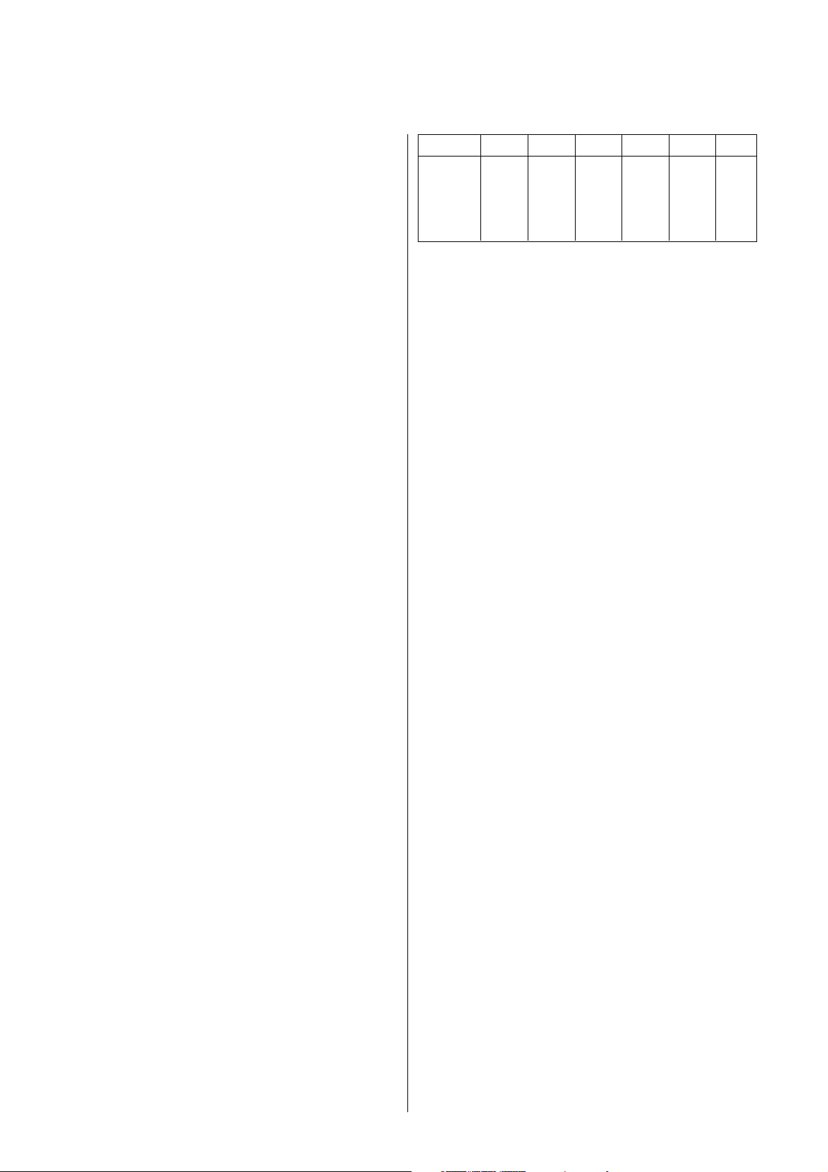
Standard pin 11 pin 13 pin 14 pin 7 pin 6 pin 5
B/G H L L L H H
I, K1 H L H H H H
D/K H H L H H H
L HHHLLL
Lí HHHHHL
Pin 11 drives input switches of IC501. Pin 11 is normally
high. During channel search (APSi), pin 11 goes
low. A low level on pins 27 and 28 of IC501
switches the video IF signal (instead of sound IF)
to the FPLL block. This is because the video band
is wider, and thus channel finding is more reliable.
Pin 13 drives the group delay correction circuitry
Pin 14 selects the output of the group delay correction
circuitry
Pin 7 selects the correct sound IF filter
Pin 6/5 drives input switches and AM demodulator, se-
lects right modulation and VCO frequency
BG standard IF block
The BG IF block is considerably simpler than the
multistandard IF block. Only one SAW filter is used and
the IIC-bus expander, group delay correction circuitry as
well as several switching transistors are omitted.
During channel search (APSi), the microcontroller (pin 47)
drives transistor T501 to conduct. A low level on pins 27
and 28 switches the video IF signal to the FPLL block in
order to make channel finding more reliable.
Tuning
Tuning is based on the APSi system (Automatic Program
search, Sorting and channel identification). The naming and
identification of the channels takes place using either the
PDC (Program Delivery Code), VPS (Video Programming
System), NI (Nation Identification) or Teletext header. Channel sorting is country dependant, and is therefore determined beforehand by the software.
The circuit IC502 operates as an IIC-bus expander (8-bit
shift register). Transistors T515 and T516 disconnect the
IIC-bus from pins 2 and 3 in order to eliminate possible
malfunctions on the IIC-bus when the TV set is switched
off. Standard definition takes place via the IIC-bus. The
microcontroller sends data to the shift register, the outputs change their state according to the data and strobe
pulse latches the outputs. The strobe pulse (high level) is
taken from the microcontroller (pin 47) to the base of transistor T517 and onward to pin 1. In addition, the base resistor (R556) of T517 operates as an indication of the installed IF module version. The value of this resistor depends on the module version. Pin 55 of the microcontroller
senses the voltage across this resistor and the base-emitter junction , and thus identifies the module version.
The data from the microcontroller determines the outputs
of IC502 according to the transmission standard as follows:
Page 12
AUDIO SECTION
r
- Sound Processor
- Audio Power Amplifier
- Headphone Amplifier
Multistandard Sound Processor, ICa2
5
General
The MSP3410D is a single-chip Multistandard Sound Processor which uses CMOS technology. The circuit is controlled by the microcontroller via the IIC-bus.
The sound processor performs simultaneous digital demodulation and decoding of NICAM-coded TV stereo
sound, as well as demodulation of FM-mono TV sound. As
an alternative, a two carrier FM system (according to the
German terrestrial specs, A2 stereo), or satellite specs can
be processed by the sound processor.
All FM modulated signals over the range 0.2 MHz to 9.0
MHz can be handled.
The sound processor can select the audio signal source,
convert analog audio signals into digital form, de-emphasize in several ways - including Wegener Panda 1, 50/75 µs
and J17, perform digital FM-identification decoding and
dematrixing, and perform digital baseband processing. It
can also control the volume separately for loudspeaker and
headphones, control bass, treble, graphic equalizer and
balance, perform pseudo stereo and basewidth enlargement, as well as convert digital audio signals into analog
form by using fourfold oversampled D/A-converters. This
provides an audio spectrum from 20 Hz to 16 kHz with a S/
N ratio of 85 dB.
The sound processor requires an 18.432 MHz crystal, whose
nominal free running frequency should be no more than
±1 kHz, which means a tolerance of ±0.005 %.
An audio signal to the sound processor can be taken from
the IF-section, scart 1, scart 2, or scart 3 / camera / VGA-
audio connector (or scart 4) sources. The source is internally selected in the sound processor. The processed audio signal is fed to several outputs such as loudspeaker
amplifier / adjustable audio output module, headphone
amplifier, scart 1 and scart 2 connectors (scart 3 optional).
The circuit also has a separate output for a subwoofer
amplifier including highpass filters for the loudspeaker
outputs and lowpass filters for the subwoofer output as
integrated into the chip. The upper barrier frequency is
programmable from 50 Hz to 400 Hz in 10 Hz steps. Depending on the programming of the upper barrier frequency, the lower barrier frequency for the loudspeaker
channels will also be changed automatically.
An IIS-bus interface with two data inputs is available for
optional audio feature purposes.
In some TV versions, the sound processor may be of type
MSP3400. The only difference is that MSP3400 cannot identify or process Nicam signals.
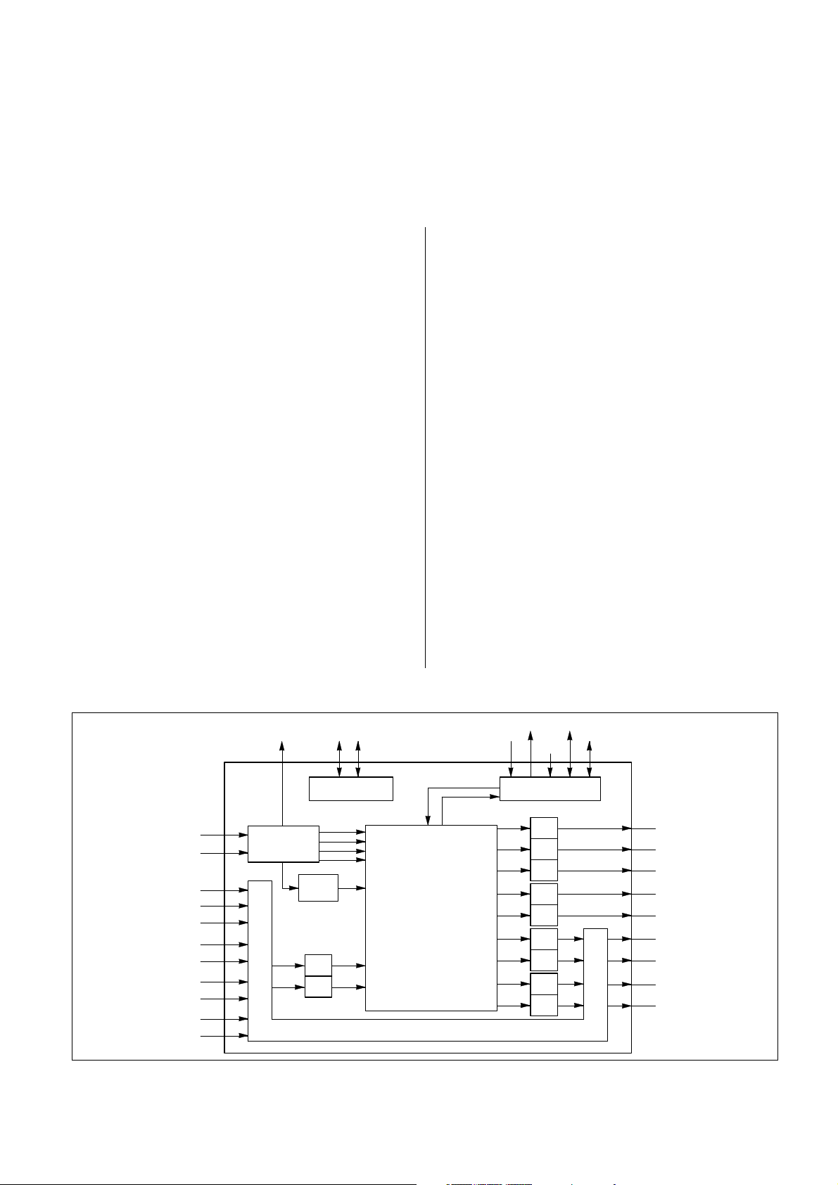
The sound processor is split into three functional blocks:
- Demodulator and decoder section
- Digital signal processing section performing audio
baseband processing
- Analog section containing two A/D-converters, nine D/
A-converters and channel selection
The simplified block diagram below shows the architecture of the MSP3410D.
Sound IF
ANA_IN 1+
ANA_IN 2+
Mono
Mono_in
SC1_IN_L
Scart 1
SC1_IN_R
SC2_IN_L
Scart 2
SC2_IN_R
SC3_IN_L
Scart 3
SC3_IN_R
SC4_IN_L
Scart 4
SC4_IN_R
ADR-bus
Demodulator
SDA SCL
2
I C-bus Interface
Ident
A/D
A/D
2
I S1/2L/R
2
I S1/2L/R
FM1 / AM
FM2
NICAM A
NICAM B
Ident
Digital
Function
Processing
SCART_L
SCART_R
SCART Switching Facilities
LOUDSPEAKER L
LOUDSPEAKER R
SUBWOOFER DACM_SUB
HEADPHONE L
HEADPHONE R
SCART1_L
SCART1_R
SCART2_L
SCART2_R
2
2
I S_DA_OUT
2
I S_DA_IN2
2
I S Interface
D/A
D/A
D/A
D/A
D/A
D/A
D/A
D/A
D/A
2
I S_CL
2
I S_WSI S_DA_IN1
DACM_L
Loudspeake
DACM_R
Subwoofer
DACA_L
Headphone
DACA_R
SC1_OUT_L
Scart 1
SC1_OUT_R
SC2_OUT_L
Scart 2
SC2_OUT_R
Page 13
6
The pin functions of the Sound
Processor:
ance of external speakers is 8 Ohm. When an external
speaker is used, the internal speaker is muted by a switch
in the speaker connector.
Pin I / O Short description
04 O DSP reset and off by low
05 O Subwoofer off by high
07 I Supply voltage +5 Vr
09 I I2C clock (SCL)
10 I/O I2C data (SDA)
11 O I2S clock
12 I/O I2S word select
13 O I2S data output
14 I I2S1 data input
18 Digital power supply +5Vr
19 Digital ground
20 I I2S2 data input
24 I MSP power-on-reset by low
25 O Headphone output, R
26 O Headphone output, L
28 O Loudspeaker output, R
29 O Loudspeaker output, L
31 O Subwoofer output
33 O Scart output, R
34 O Scart output, L
36 O Scart output, R
37 O Scart output, L
38 Volume capacitor (Hp amp)
39 Analog power supply +8.0V
40 Volume capacitor (Ls amp)
42 Analog ref V, high V part
43 I Scart input, L
44 I Scart input, R
46 I Camera input, L
47 I Camera input, R
49 I Scart input, L
50 I Scart input, R
52 I Scart input, L
53 I Scart input, R
54 Ref voltage IF A/D conv
55 I Mono input
57 Analog power supply +5Vr
58 I IF input 1
59 I IF input common
60 I IF input 2 (Tuner SIF)
62 I Crystal osc 18.432 MHz
63 O Crystal osc
Headphone Amplifier, ICa3
Audio signals from the sound processor are fed to the inverting input pins 2 (L) and 6 (R). Outputs to the headphone
connector are from pins 1 (L) and 7 (R). There is a switch in
the headphone connector that informs the microcontroller
(pin 1), that headphones are connected. The headphone
volume control then appears in the OSD in addition to the
loudspeaker volume control.
Audio Power Amplifier, ICa1
The audio signal is amplified using the TDA2616 dual channel hi-fi Audio Power Amplifier. The amplifier has a builtin protection system against short circuits and thermal
overloads. It also has an internal input mute circuit that
silences unwanted signals at the inputs when the TV set is
switched on or off.
Audio signals from the audio processor are fed to pins 1
(L) and 9 (R). A logical low on pin 2 mutes the amplifier.
The mute control signal is taken from the microcontroller
(pin 51) via transistors ta10, ta4 and ta3. A high level on
microcontroller pin 51 causes a so-called “central mute”,
which means that each of the audio power amplifiers are
muted.
The supply voltage +28 V is taken from the power supply
to pin 7. The amplified audio signals for the loudspeakers
are output on pins 4 (L) and 6 (R). The impedance of the
internal loudspeakers is 8 ohm and the minimum imped-
Page 14
VIDEO SECTION
7
The video section is divided into the following functional
blocks:
- Video Matrix Switch / Scarts
- Colour Decoder / Sync Processor
- Baseband Delay Line
- Feature Boxes
- RGB Video Processor
- CRT module
- Teletext
Video Matrix Switch, ICq1
The TEA6417 is an IIC-bus controlled signal switch, which
makes it possible to switch 8 input sources to 6 outputs.
Each output can be connected to only one input, but one
input may be connected to several outputs. The bandwidth
is 15 MHz and nominal gain from input to output is 6.5 dB.
All switching possibilities are controlled via the IIC-bus
using pins 2 (SDA) and 4 (SCL). The circuit operates with
+10 V supply voltage, that is fed to pins 9 and 12. The +10
V is regulated from +12Vr by zener diode Zdq1.
The inputs and outputs are connected as follows:
Input Signal Source
1 CVBS Scart 3
3 CVBS Scart 1
5 C Scart 2
6 CVBS / Y Scart 2
8 CVBS / Y Cam connector
10 C Cam connector
11 CVBS Tuner
20 CVBS PIP tuner
Output Signal Target
13 CVBS / Y Decoder / Comb filter
14 C Decoder / Comb filter
15 CVBS / Y PIP module
16 C PIP module
17 CVBS / Y Scart 2
18 CVBS Teletext
The system is based on the “P50” standard and enables,
for example, transferring of channel tuning information and
EPG (Electrical Program Guide) programming.
Scart 2
In addition to the S-VHS input possibility, scart 2 is designed
to output the S-VHS signals, which are taken from the camera connectors. Output of the luminance signal takes place
via transistor Tq1 and chrominance via tt3 and tt2.
Scart 2 also operates as an AV-link connector.
Scart 3 (option)
Scart 3 is an optional connector having the same characteristics as scart 1.
More detailed information can be found in the section entitled “Options, TA710”.
Colour Decoder / Sync Processor, ICd1
General
The TDA9143 is an IIC-bus controlled, alignment-free PAL /
NTSC / SECAM decoder / sync processor.
The colour decoder is able to process CVBS as well as Y / C
signals. The internal fast switch can select either the Y signal with the UV input signals, or YUV signals made up of
RGB input signals.
The sync processor provides a two level sandcastle pulse
(SC), a horizontal sync pulse (HA) and a vertical sync pulse
(VA).
Input switches
The circuit has a two pin input for the CVBS (pin 26) or Y / C
(pins 26 and 25) input signals. Selection between the signals is carried out using the IIC-bus.
RGB colour matrix
The RGB signals from scart 1 (or scart 3 ) connector are fed
to input pins 19 (B), 20 (G) and 21 (R). The RGB colour matrix converts RGB signals into the YUV signals. The desired
input signal, between the converted YUV and decoded YUV
signals, is selected by the fast switch. This switch is controlled by the fast blanking signal on pin 18.
Scart 1
Scart 1 is fully connected, thus RGB input is also available
from it . In RGB mode, the fast blanking signal from scart
pin 16 is fed to the colour decoder pin 18 and via tq3, tq4,
Cq32 (and NAND gate icf4-4) to the microcontroller pin 6.
The RGB status signal is fed to the microcontroller in order
to activate the correct H-shift setting. It also enables the
colour decoder to choose the input between the RGB signal and the processed YUV signals. Selection takes place
by a switch block in the colour decoder via the IIC-bus.
Scart 1 has a fixed output connection for the Tuner CVBS
from scart pin 19 via transistors tq9 and Tq2.
Scart 1 also operates as an AV-link connector. The AV-link
output is from microcontroller pin 2, onward via transistor
tq7 and scart pin 10. The AV-link input is from the same
scart pin, onward via diode dq4 and transistor tq8 to the
microcontroller pin 63. The AV-link system makes it possible to transfer data between the TV set and e.g. a video
recorder.
Luminance processing
From the input pin 26, the CVBS / Y signal is fed via the Y
clamp circuit to the gyrator-capacitor type notch filters, including adjustable luminance delay and chrominance trap.
The luminance delay compensates the delay, that is caused
by the external baseband delay line for the UV signals. The
chrominance trap can be switched to 4.43 MHz (PAL / NTSC),
4.28 MHz (SECAM) or 3.58 MHz (NTSC). Switching is con-
trolled by the standard identification circuit. PAL Y, NTSC
3.58 Y (from the comb filter ) and S-VHS Y signals bypass
the chrominance notch filters in order to preserve the signal bandwidth. The bypass function takes place automatically via the IIC-bus in S-VHS mode and in PAL / NTSC 3.58
reception, if the comb filter is installed. After the chroma
trap, the Y signal is fed to the switch stage and is output
from pin 12 to the feature box module.
Page 15

8
Chrominance processing
From the input switch, the CVBS / C signal is fed through
the ACC amplifier to the chroma bandpass filters. PAL C,
NTSC 3.58 C (from the comb filter) and S-VHS C signals
bypass these bandpass filters in order to preserve the signal bandwidth. The chrominance is then fed to the standard identification and colour decoder stages.
The standard identification circuit is a digital circuit with
no external components. The crystals on pins 30 (reference crystal) and 31 (second crystal) specify the standards
which can be decoded. The IIC-bus is used to indicate which
crystals are connected in order to allow proper setting of
the calibration circuits. The components on pin 29 form
the colour PLL filter. Pin 23 drives the multiplexer circuit
on the comb filter module to bypass the S-VHS signals in
the multiplexer (“L”) or to feed signals onwards to the comb
filter IC (“H”). In addition, pin 23 feeds out the subcarrier
frequency (Fsc) of the active crystal to the comb filter IC.
After the PAL / NTSC demodulator and SECAM
demodulator, the signals are taken to the switch stage,
which is controlled by the standard identification circuit.
Finally, the colour difference signals are output to the
baseband delay line from pins 2 (U) and 1 (V).
From the delay line, the colour difference signals are input
to pins 3 (U) and 4 (V), then onward to the switch stage
and output from pins 14 (U) and 13 (V) to the feature box
module.
Sync processing
The CVBS / Y signal is fed through the sync separator to
the horizontal PLL and to the vertical sync separator.
The main part of the sync circuit is a 432 x fH (6.75 MHz)
oscillator. This frequency is divided by 432 to lock phase
discriminator 1 to the incoming signal. The time constant
of the loop can be selected to be either fast, auto or slow
mode using the IIC-bus. The free-running frequency of the
432 x fH oscillator is determined by a digital control circuit,
which is locked to the active crystal. Components on pin
24 form the horizontal PLL. The phase loop can be unlocked
using the IIC-bus. This is to facilitate On Screen Display
information. If there is no input signal or a very noisy signal, the phase loop can be unlocked to give a stable line
frequency and hence a stable OSD.
The horizontal sync pulse (HA) is fed from the timing generator via output pin 17 to the Feature box.
The vertical divider system has a fully integrated vertical
sync separator. The divider can handle both 50 Hz and 60
Hz systems. It can either determine the field frequency
automatically or it can be set to the desired frequency using the IIC-bus.
The divider system consists of a line counter, a norm counter , a timing generator, and a controller. The system operates at 432 times the horizontal line frequency. The line
counter receives enable pulses at twice the line frequency,
so that it counts two pulses per line. This count result is
fed to the controller. The controller can be in one of three
count states, norm, near-norm or no-norm. When the counter is in the norm state, it automatically generates a vertical sync pulse (VA) from the timing generator. The VA pulse
is fed via output pin 11 to the Feature box.
Noise detector
The decoder includes an internal S/N ratio detector, which
was originally designed to control the PALplus signal process. During PALplus transmission, the detector measures
the S/N ratio of the input signal on pin 26. When the S/N
ratio is over 20dB, the signal is accepted and the helper
signal is processed in the PALplus decoder. If the S/N ratio
is below 20dB, the PALplus process is disabled, and the
signal is handled as a normal signal. The detector can be
activated / deactivated via the IIC-bus.
In the Multi Concept, this detector is used to drive the APSi
system to accept or bypass tuned channels. The detector
controls the APSi system via the IIC-bus and it works only
during the automatic channel search.
However, the limit value of the bypass criteria (fixed 20dB)
seems to be too high for this purpose and therefore the
APSi may be too sensitive and bypass channels that it could
accept.
On the other hand, if the tuning system does not include
any signal level qualification, the APSi system accepts all
multiple and very noisy channels.
Utilizing an existing detector and avoiding both above
mentioned disadvantages, an external LPF filter is implemented. This filter is located at the luminance / CVBS input
(pin 26) and it consists of switching transistors tq10 / tq11,
and RC filter rq85 / cq45.
The RC-coupling is designed to filter high frequencies
(noise) from the luminance / CVBS signal.
When the S/N ratio of the tuned signal on pin 26 is over
20dB, the filter is not activated, but the channel is accepted
as such and it will be memorized and named.
If the S/N ratio is below 20dB, the detector causes a high
level on output pin 16. Transistor tq11 conducts and the
RC-coupling filters noise from the signal improving the S/
N ratio at the decoder input. When this noise-filtered signal is fed to the detector, it considers the S/N ratio to be
better than it actually is and accepts it. This channel will be
memorized, but not named.
In any case if the S/N ratio of the noise-filtered signal stays
below 10dB, it will be completely bypassed.
By tricking the detector in this way, the signal level qualification is reduced from an S/N ratio of 20dB to 10dB.
Sandcastle
The sync part also generates a two level sandcastle pulse
(SC) from pin 10. This pulse is used only for timing purposes in the baseband delay line.
IIC-bus
The decoder / sync processor is connected to the IIC-bus
via pins 5 (SCL) and 6 (SDA).The bus address is determined
by connecting pin 22 to +8 V.
The output pin 16 controls the filtering method of the comb
filter, either PAL 4.43 MHz (“L”) or NTSC 3.58 MHz (“H”).
The input / output pin 15 is primarily used to detect whether
the comb filter module is installed or not, by checking the
transistor tc3 (base-collector junction). In addition, pin 15
controls the comb filter IC to be in the filtering mode (“H”)
or in the internal bypass mode (“L”).
Baseband Delay Line, ICd3
General
The circuit TDA4665 is a delay line which requires no adjustments. It includes two colour difference comb filters
and uses switched capacitor techniques.
Each comb filter consists of an undelayed signal path and
a 64 µs delayed signal path.
In PAL mode, comb filters operate as a geometric adder to
carry out the requirements of PAL demodulation.
In NTSC mode, the comb filters suppress cross-colour interference.
In SECAM mode, the circuit repeats the colour difference
signal on consecutive horizontal scan lines.
Page 16
Functional description
The colour difference signals are fed to input pins 14 (U)
and 16 (V). First the signals are clamped, and then they are
fed through pre-amplifiers to the undelayed / delayed signal paths. All the switching signals needed in the delay
process are generated from the 3 MHz master clock frequency. This frequency is divided from the internal 6 MHz
VCO, which is line-locked by the sandcastle pulse (SC). The
SC pulse taken from the sync processor is fed to pin 5.
Delay processed colour difference signals are fed through
the addition circuits to the output buffers and are finally
output on pins 12 (U) and 11 (V).
Feature boxes, DB7**
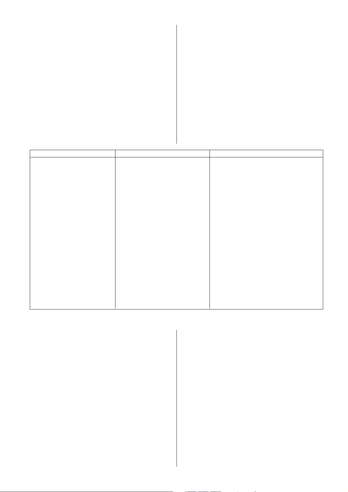
The feature box has two main functions, to perform the
conversion of the 50 (60) Hz scan to 100 (120) Hz scan format and to improve the picture quality. Depending on the
Feature DB711 DB710
100 Hz flicker reduction - field repetition - median interpolation
Line flicker reduction - no - median filter
Noise reduction (Y / C) - no - motion adapted
Aspect ratio conversions
- horizontally - ±12.5 and ±25 % - ±12.5 and ±25 %
- vertically - by deflection - +12.5 and +25 % (by DSP)
- hor picture position - fully programmable - fully programmable
- lift - no - yes
- side panels - programmable grey - programmable grey
Picture sharpening - vertical / horizontal peaking - vertical / horizontal peaking
- CTI, LTI - CTI, LTI
Histogram equalizing - yes - yes
Still picture - yes - yes
A/D conversion - YUV 4:1:1 signal format - YUV 4:1:1 signal format
- 8-bit per component - 8-bit per component
- input signal amplitude adapted - input signal amplitude adapted
- sampling rate - 13.5 MHz - 13.5 MHz
D/A conversion - Y-component 9-bit - Y-component 9-bit
- U- and V-component 8-bit - U- and V-component 8-bit
- sampling rate - 20.25 MHz ... 36 MHz - 20.25 MHz ... 36 MHz
Field memory - 3 Mbit (1 x 3 Mbit) - 6 Mbit (2 x 3 Mbit)
Synchronizing - line locked operation - line locked operation
- crystal based sync generation - crystal based sync generation
chassis version, there are few different feature boxes with
more or less variant features. The whole signal processing
takes place digitally and all functions are controlled using
the IIC-bus.
The basic version is DB711, that contains only one 3 Mb
field memory. The use of one field memory allows the conversion of 50 (60) Hz video to 100 (120) Hz video, but not
line flicker and noise reduction or vertical zooms. This
module is designed for TV sets with a 4:3 picture aspect
ratio.
The DB710 version contains two 3 Mb field memories, so
noise reduction and vertical zooms are also implemented.
The DB710 (and DB700) are designed for TV sets with both
a 4:3 and 16:9 picture aspect ratio.
The DB700 version is called a “full feature” version, that
includes in addition to the features of DB710, a signal interface in accordance with the VGA standard.
9
Feature box DB711
The main components of the DB711 are an A/D converter,
field memory (FM), picture quality improvement circuit
(IQTV2), digital phase locked loop (DPLL) and deflection
controller.
Y, U and V inputs
The luminance (Y) and colour difference signals (U and V)
are taken from the colour decoder to the module connector Q101, pins 6 (Y), 7 (U) and 8 (V). Each signal is first
amplified and then low pass filtered. After that the signals
are fed via buffer transistors to the A/D-converter, pins 63
(Y), 50 (U) and 31 (V).
Analog to digital converter, ic9
Analog to digital conversion is carried out using A/D-converter circuit TLC5733, which contains three separate 8-bit
A/D-converters. Each signal is clamped using the horizontal sync pulse (HOUT1) on pin 55 and then converted to
digital form. The converters sample the input signals at a
13.5 MHz sampling rate. The sampling frequency is taken
to pin 56. The converters are controlled by reference
voltages REFH (pins 61, 52 and 29) and REFL (pins 1, 48
and 33).
If an overflow is detected, the reference voltages will be
either increased or decreased. Information about a possible overflow is taken from the luminance output data (pins
6...13) and fed to the NAND gate ic28 and onward to the
DPLL circuit ic11 pin 42 (ADC_OVFL). The circuit detects
the overflow data and if necessary, it changes the width of
the pulses on pin 43 (PWM_REF). These width modulated
pulses are fed to the low pass filter consisting of transistors t1 and t9 and associated capacitor network. The low
pass filter generates both voltages, the REFH and REFL,
and these are fed to control the A/D-converters.
After converters the signals are fed to the output format
multiplexer, which is controlled by pins 45 (mode1) and 46
(mode0). The combination of a logical low on both pins
causes the output data format of the YUV signals to be
4:1:1. The U and V components have 1/4 of the signal
strength of the Y component.
The luminance data bus (pins 6...13) is eight bits wide and
the chrominance data bus (pins 17...20) four bits wide.
Page 17
10
Field memory, ic14
Field Memory 1 (FM1) is a 3 Mb, high-speed Dynamic Random Access Memory (DRAM). The circuit is used as a
memory circuit in the 50 to 100 Hz upconversion and in
certain horizontal zoom functions.
The luminance and chrominance data are input from the
A/D-converter to pins 2...13.
The write operation is performed using the input control
signals RSTW (reset write) on pin 15, SWCK (serial write
clock) on pin 14 and ENW (enable write) on pin 16. The
write clock (SWCK / CLK27_1) frequency is 27 MHz. The
ENW signal enables memory writes only on every second
clock cycle.
The read operation is performed using the read output
control signals RSTR (reset read) on pin 22, SRCK (serial
read clock) on pin 23 and ENR (enable read) on pin 21.
The read clock (SRCK / CLK) frequency varies depending
on the picture format. The IQTV is able to generate the
following formats (implementation depends on the feature
box and software):
36.000 MHz = - 25.0 % hor compression
30.375 MHz = - 12.5 % hor compression
27.000 MHz = 0 no compression / no expansion
23.625 MHz = + 12.5 % hor expansion
20.250 MHz = + 25.0 % hor expansion
All vertical compression is carried out by the deflection
processor. Only the DB710 and DB700 comprise the vertical expansions (FM2 required).
The luminance and chrominance data are output to the
IQTV2 circuit from pins 24...35.
IQTV2 circuit, ic18
The main function of the IQTV2 (Improved Quality TV) circuit is to perform the upconversion, which reduces the
flicker caused by interlacing. The idea of the upconversion
is that the interlaced 50 (60) Hz scan will be converted to a
100 (120) Hz scan format.
The flicker reduction (upconversion) in the DB711 module
is based on a field repetition algorithm for both luminance
and chrominance signals. The field repetition method uses
zero degree interpolation and displays the original field
twice.
The characteristics of the IQTV2 make it possible to utilize
both the horizontal and vertical zoom functions, but because there is only one field memory, only the horizontal
zoom can be utilized. Thus all vertical zoom functions are
performed using the deflection controller circuit.
Picture sharpening is implemented not only in the horizontal direction, but also in the vertical direction. The peaking stage consists of high pass and band pass filters which
emphasize the middle band frequency range where most
of the details and edges are located.
The colour transient improvement (CTI) makes the slopes
of colour edges steeper by controlling the inputs between
the delayed, look ahead and current chrominance signals.
A new feature in the CTI of the IQTV2 circuit is that the
center of the transient always stays at the same point in
comparison with input and output signal.
The luminance transient improvement (LTI) is performed
by taking the 3-point median of three intermediate signals,
peaked, maximum and minimum. As a result of the LTI
process the luminance transients are made steeper without any undershoots or overshoots.
The histogram equalization (HEQ) system is designed to
carry out an automatic contrast enhancement. The system
is designed to give a uniform histogram for the output picture signal, changing the original pixel values for new ones
using a non-linear mapping. As a result, both under and
over contrasted picture signals are equalized to have the
desired contrast and gray level distribution.
Pin description of ic18:
Pin Symbol Description
1, 5-12, 14-15,
18-21, 100 D0_FM1...
D15_FM1 Data input from FM1
2, 16, 41,
56, 81 +3.3V (core) Power supply for logic
3, 28, 61, 77 +5V (i/o, AC) Power supply for I/O
4, 29, 60, 69 GND (i/o, AC)
Ground for I/O
13, 34, 78 +5V (i/o, DC) Power supply for I/O
17, 37, 57,
79, 99 GND (CORE) Ground for CORE
22 FM1_ENR Read enable, FM1
23 FM1_ENW Write enable, FM1
24 FM1_RSTW Reset write, FM1
25 HS_IPLL Horizontal sync
26 FM2_ENW Write enable, FM2
27 FM2_ENR Read enable, FM2
30 CLK_IPLL
(CLK27_1) System input clock
(27 MHz)
31 CLK_OPLL
(CLK) System output clock
32 VS_50 Vertical sync
33 HS_OPLL Output horizontal sync
35 HS32 32 kHz horizontal sync
36 FM_RSTR Reset, FM2W/R, FM1R
38 SDA IIC-bus, serial data
39 SCL IIC-bus, serial clock
40 FSY Format sync for ADC
42 +5V (analog) Analog supply voltage
for DAC
43 VBIAS Analog
44, 47, 49, 51 GND (analog) Ground for DAC
45 VT Analog
46 Vref Current reference
for DAC
48 AY Analog Y output
50 AV Analog V output
52 AU Analog U output
53 RST System reset
54 TEST_EN Test mode enable
55 VS_50_100 Double frequency
vert sync
58-59, 62-67,
70-76, 80 Q0_FM2...
Q15_FM2 Data output to FM2
68 DIG_OUT8 9th bit in digital output
82-89, 91-98 D0_FM2...
D15_FM2 Data input from FM2
90 SYNC_SEL Selection of sync mode
After digital signal processing (DSP), the IQTV2 circuit converts the signals to analog form and outputs them from
pins 48 (Y), 52 (U) and 50 (V).
The colour difference signals are low pass filtered and output from module pins Q102-3 (U) and Q102-2 (V). The luminance signal is first amplified by transistors t18 and t19,
then the signal is low pass filtered and output from module pin Q102-4.
Page 18
DPLL1 circuit, ic11
The DPLL (Digital Phase Locked Loop) circuit generates all
line locked clock and sync signals for the whole digital signal processing system. The circuit is IIC-bus controlled and
it needs only a few external components, one of them a 27
MHz crystal. The 27 MHz clock operates as a main clock,
from which the other clock frequencies are generated using suitable factors.
Pin description of ic11:
Pin Symbol Description
11
The horizontal (HDFL) and vertical (VDFL) sync signals from
the DPLL1 are fed to input pins 13 and 12 to synchronize
the circuit.
The horizontal flyback pulse is taken from the horizontal
output stage to input pin 1.
Horizontal drive signal
From the horizontal detector stage, the horizontal sync signal is fed to the horizontal counter, the horizontal place
control, the phase 2 loop, and finally output from pin 20 to
drive the horizontal driver stage. The H-phase adjustment
is performed in the horizontal position control stage using
the IIC-bus.
1 HSYNC1 Horizontal sync from sync
processor
5 VSYNC1 Vertical sync from sync
processor
7 HOUT1 Horizontal sync for ADC and
IQTV2
9 CLK27_1 27 MHz main clock for FM1
and IQTV1
11 CLK13_5_1 13.5 MHz clock for ADC
13 VOUT1 Vertical sync for IQTV2
22 CLK27_2 27 MHz main clock for
deflection controller
24 HS_GSCART Horizontal sync from VGA
(DB700)
26 HSYNC2 Horizontal sync from VGA
(DB700)
27 VS_GSCART Vertical sync from VGA
(DB700)
28 CLK Format dependant clock for
FM1/2 and IQTV2
29 VSYNC2 Double frequency vert sync
from IQTV2
30 HOUT2 (HDFL) Hor sync for IQTV2 and
deflection controller
31 VOUT2 (VDFL) Vert sync for IQTV2 and
deflection controller
33 FORMAT_VGA Low by DB711/710, high by
DB700
35, 36 XTALCLK 27 MHz crystal (for main
clock)
37 FORMAT_MEM High by DB711, low by
DB700/710
40, 41 SDA / SCL IIC-bus, serial data and clock
42 ADC_OVFL Overflow data from ADC
43 PWM_REF Output of width modulated
pulses for ADC
Vertical drive signal
From the vertical detector stage, the vertical sync signal is
fed to the vertical place control, the vertical place generator, the vertical geometry stage and finally the differential
current vertical drive signals are output from pins 10 and
11 to drive the vertical deflection circuit ICs1. Vertical amplitude, S-correction and V-shift are controlled in the vertical geometry stage via the IIC-bus. The reference current
for both the vertical and E-W geometry processing is determined by resistor r68 on pin 8.
E-W drive signal
The E-W drive signal is a single ended current output and
it is taken out from pin 6. The control parameters: E-W
width, E-W parabola/width ratio, E-W corner/parabola, and
E-W trapezium are included in the E-W geometry processing stage. All of these controls can be set using the IICbus.
EHT compensation
Both the vertical and the E-W drive outputs are modulated
for EHT compensation via pin 7. The EHT information is
taken from DST pin 8 (“static” information) and from Ck31
/ Rk58 and Ch21 / Rh29 (dynamic information).
Sandcastle
The TDA9151 generates a two level display sandcastle pulse
(DSC). The 2.5 V level is used for horizontal and vertical
blanking, and the 4.5 V level for video clamping. The DSC
is output from pin 2 and it is used for the timing of the RGB
Video processor ICt1.
In addition, pin 2 operates as an input pin for the vertical
guard. The DSC pulse is connected to pin 1 of the vertical
deflection circuit. In possible fault cases, the vertical IC will
supply a voltage level of 2.5 V, which causes blanking of
the screen.
Deflection Controller TDA9151, IC17
The TDA9151 circuit is an IIC-bus controlled synchronization and deflection processor having horizontal and vertical drive outputs and an East-West correction drive circuit.
Input signals
The serial data (SDA) and serial clock (SCL) are connected
to pins 17 and 18.
The 27 MHz line locked clock pulse (CLK27_2) from the
DPLL1 is fed to pin 14. The internal synchronous logic uses
the LLC as a system clock. It is important to realise that the
circuit will not operate without the LLC, it will switch off
the outputs and will not perform any operations. The LLC
frequency is divided by two by connecting the line-locked
clock select input pin 5 (LLCS) to ground. This activates
the prescaler stage and creates a line duration of 32 µs.
Page 19
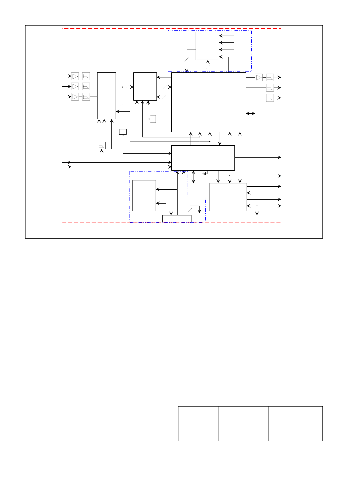
12
Feature box
DB711 / 710 / 700
Y
U
V
VSA / VSYNC1
HSA / HSYNC1
A/D-C
YUV
INIT,CLP
CLK
A/D-C_REFV
Y
&
12
8
RSTR
FM1
3 Mb
ENW
ENR
RSTW
SWCK
SRCK
CLK
27 MHz
13.5 MHz
EEPROM
VCLK
DDC1
interface
SDA
SCL
In DB700 only
In DB700 and
DB710 only
YUV
12
FM_RST
D0...D11_FM1
12
FM1_ENW
FM1_ENR
2
&
FM1_RSTW
CLK13.5_I
OVFL
PWM_REF
VSYNC1
HSYNC1
HSYNC
VSYNC
VGA
VS_50
IIC-bus
3
FM2
3 Mb
YUV
IQTV2.1
DB711
UP-C, HFC, HEQ
CTI, LTI, Peaking
D/A-C
DB700/710
UP-C, FC, NR, HEQ
CTI, LTI, Peaking,
D/A-C
CLK_IPLL
CLK27_I
DPLL1.02
27 MHz
RGB VGA
to Xtpp
SWCK
SRCK
RSTW
RSTR
12
HS_IPLL
27 MHz
LLC
Deflection
controller
FM2_ENW
FM2_ENR
VS_50_100
CLK
VA
VA HA
CLK_OPLL
VS_50_100
FM_RST
AY
AU
AV
CLK_OPLL
IIC-bus
HS_OPLL
HSYNC_O
VSYNC_O
DSC
EHT, HFB
HD, VD, EW
IIC-bus
IIC-bus
Block diagram of the Feature boxes DB711, 710 and 700
Feature box DB710
The basic functions of the DB710 are similar in principle to
the DB711. The only visible difference is that the DB710 is
equipped with two field memories, FM1 and FM2. This allows noise reduction and vertical zoom (vertical format
conversion) functions to be implemented.
The upconversion from 50 to 100 Hz in the DB710 is based
on a median interpolation algorithm that reduces both the
field and line flicker. The median filter method uses a 7point adaptive median interpolator, whose sampling window consists of 7 samples, taken in horizontal, vertical and
temporal directions. The 7-point median output will be replaced with 3-point vertical median output, if a difference
signal exceeds the externally determined threshold level.
The noise reduction system consists of an adaptive
weighted average post-filter, that is based on the so-called
motion adaptive temporal recursive averaging filter. The
system is used not only for noise reduction, but also to
reduce the cross effects. The noise reduction affects both
the luminance and chrominance components. As mentioned above, the noise reduction function requires an additional field memory. This field memory, FM2 is identical
to FM1 and it is connected to the IQTV2 circuit in a similar
way.
The characteristics of the vertical format conversion of the
IQTV2 circuit make it possible to always display all vertical
zoom modes with a full vertical resolution of 576 active
lines. This is due to the digital signal processing and linear
vertical interpolation.
Feature box DB700
The functional features are similar to DB710; median interpolation, noise reduction, full vertical resolution etc. In addition to these features, the DB700 is equipped with a VGA
(video graphics array) interface in order to make it possible to use the TV set as a monitor for a personal computer.
For this reason, an additional memory circuit is needed.
The memory circuit ic3 is a serial EEPROM, that is pre-programmed with the data needed for automatic configuration of the display controller in the computer via the display data channel 1 (DDC1).
The vertical and horizontal sync signals from the VGA connector are fed via inverting schmitt triggers and fed onward to pins 27 (vert sync) and 24/26 (hor sync) of the
DPLL1.
The analog RGB signals are fed through the module without any processing to the RGB video processor ICt1 via the
connector Xtpp on the main board, or via the PIP module,
if installed. If sound signals are also taken from the PC,
they are input via Scart3 + VGA audio module TA710.
The following VGA modes are available:
Resolution Line frequency Field frequency
640 x 480 31.5 kHz 60 Hz
640 x 350 31.5 kHz 70 Hz
640 x 400 31.5 kHz 70 Hz
Page 20
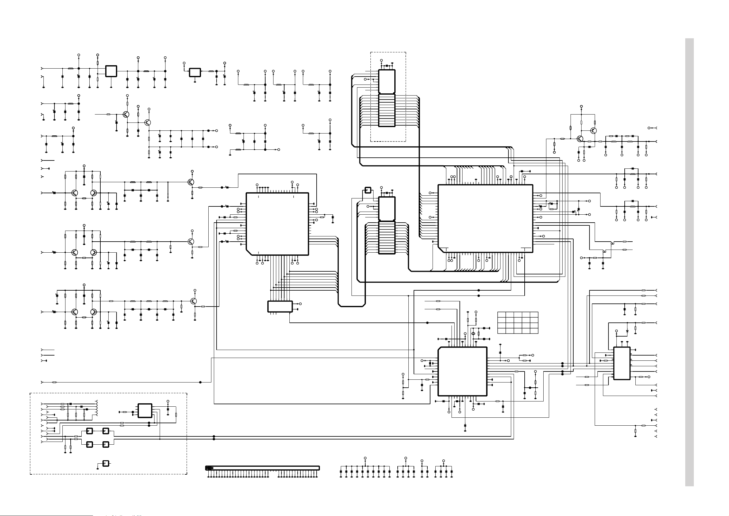
Q101-3
t
t
t
Q101-3
Q101-4
Q101-4
Q101-1
Q101-1
Q101-2
Q101-2
Q101-5
Q101-5
Q101-11
Q101-11
Q101-9
Q101-9
Q101-16
Q101-16
Q101-8
Q101-8
Q101-7
Q101-7
Q101-6
Q101-6
Q101-14
Q101-13
Q101-12
Q101-10
Q101-10
Q104-1
Q104-2
Q104-3
Q104-4
Q104-5
Q104-6
Q104-7
Q104-8
Q104-9
Q104-10
Q104-11
Q104-12
Q104-13
Q104-14
Q104-15
O N LY D B 7 0 0
7 V f b
D
D
1 2 V p
D
D
8 V p
V i n
U i n
Y i n
SDA
SCL
HSNCI
D
VSNCI
D
C211
10n
D
VGA_R
VGA_G
VGA_B
L5
L5
10u
10u
C60
C60
22u
22u
C70
C70
22u
22u
C90
C90
22u
22u
R161
1k0
DB700/710 Feature module
7V
L1
L1
10u
10u
C210
10n
D
12V
12V
L3
L3
10u
10u
C43
C43
C44
C44
22u
22u
100n
100n
D
D
D
D
VCC8
VCC8
TP24
C50
C50
C49
C49
100n
100n
100u
100u
D
D
D
D
R5
R5
R7
R7
15k
15k
22R
22R
T2
T2
BFS20
BFS20
R8
R8
R6
R6
470R
470R
4k7
4k7
A
A
A
A
R15
R15
R17
R17
22R
22R
15k
15k
T4
T4
BFS20
BFS20
R16
R16
R18
R18
470R
470R
4k7
4k7
A
A
A
A
R25
R25
C80
C80
100u
100u
A
A
R209
R210
R211
DD
D
R193
1k0
R27
R27
15k
15k
22R
22R
T6
T6
BFS20
BFS20
R28
R28
R26
R26
470R
470R
3k9
3k9
A
A
A
A
C160
470n
0R0
0R0
C161
0R0
R108
R107
75R
75R
R191
1k0
1k0
R192
R194
1k0
DD
TP22
C33
C33
C34
C34
220u
220u
100n
100n
D
D
D
D
TP23
C45
C45
100n
100n
A
A
12V
12V
C61
C61
10n
10n
A
A
R9
R9
180R
180R
12V
12V
C71
C71
10n
10n
A
A
R19
R19
240R
240R
12V
12V
C81
C81
10n
10n
A
A
R29
R29
180R
180R
R G B O U TV G A - I N
470n
C162
470n
R109
75R
1
IC2-1
74F14
1
5 9 8
IC2-3
74F14
12V
12V
R73
R73
4k7
4k7
1
4
R75
4k7
D
PWM_REF
R10
R10
R12
R12
470R
470R
15k
15k
T3
T3
BFS20
BFS20
R11
R11
R13
R13
4k7
4k7
220R
220R
A
A
A
A
R22
R22
R20
R20
15k
15k
470R
470R
T5
T5
BFS20
BFS20
R21
R21
R23
R23
180R
180R
4k7
4k7
A
A
A
A
R32
R32
R30
R30
15k
15k
470R
470R
T7
T7
BFS20
BFS20
R33
R33
R31
R31
220R
220R
3k9
3k9
A
A
A
A
Q105-1
Q105-2
Q105-3
Q105-4
Q105-5
Q105-6
21 3 4
IC2-2
74F14
6
IC2-4
74F14
D
IC2-5
74F14
IC1
IC1
PQ05RF1
PQ05RF1
IN
ON/OFF
GND
R72
R72
100k
100k
A
A
A
A
R195
A
A
1
1
1
1011
3
C62
C62
100u
100u
C72
C72
100u
100u
0R0
C82
C82
100u
100u
D
D
OUT
VGA_HSYNC
VGA_VSYNC
A
A
A
A
A
A
A
A
2
C51
C51
47u
47u
C63
C63
100n
100n
C73
C73
100n
100n
C83
C83
100n
100n
T9
T9
BC847B
BC847B
R215
D
R212
100R
R213
100R
VCC
VCC
TP13
C35
C35
C36
C36
100n
100n
100u
100u
D
D
D
D
VCCA
R91
VCCA
VCCA
820R
R1
R1
820R
820R
R2
R2
C52
C52
820R
820R
100n
100n
A
A
A
A
L6
L6
33u
33u
C65
C65
6p8
6p8
C64
C64
C66
C66
180p
180p
82p
82p
A
A
A
A
L8
L8
33u
33u
C75
C75
6p8
6p8
C74
C74
C76
C76
82p
82p
180p
180p
A
A
A
A
L10
12u
C85
C85
5p6
5p6
C84
C84
C86
C86
82p
82p
33p
33p
A
A
A
A
IC3
IC3
24LC21
24LC21
1
NC.
2
NC.
TP60
10k
3
WP
D
D
TP58
TP59
L2
L2
10u
10u
VCLK
VCCA
L7
L7
27u
27u
L11
12u
VCC
SCL
SDA4VSS
C67
C67
22p
22p
L9
L9
27u
27u
C77
C77
22p
22p
C87
C87
27p
27p
T1
BC847B
R3
75R
R4
10R
A
VCCA
C37
100u
A
C53
1u0
A
C55
1u0
A
C68
68p
A
C78
68p
A
L12
12u
C115
22p
C88
68p
A
8
7
6
5
A
TP14
C38
100n
VCC
R14
470R
A
D
C153
100n
A
A
A
C54
100n
C56
100n
R24
470R
VCC
IC4
LD1117
IN OUT
GND
D
C58
C57
1n0
1n0
12V
12V
T15
T15
BC847B
BC847B
R99
R99
200R
200R
200R
200R
R98
R98
A
A
12V
T14
BC847B
R97
200R
200R
R96
A
12V
T13
BC847B
R95
200R
R34
560R
A
C114
18p
A
R214
R94
200R
A
TP18
10k
ECO2_VIDEO_SHIELD
VCCIQ3
VCCIQ3
L14
10u
TP51
C19
100n
TP4
REFH
C59
1n0
TP5
REFL
TP41
TP42
A101
2
4
1
3
D
D
D D
5
TP1
TP3
A
A
TP2
D D D
VCC
C18
100u
DD
C69
1u0
C79
1u0
C168
2n2
C169
2n2
C89
1u0
7
6
L30
10u
VCC
VCC
L4
L4
10u
10u
C46
C46
22u
22u
L13
L13
10u
10u
D
49
A
GND_B
50
BIN
51
B_AVCC
VCCA
52
RTB
REFH
53
CLPVB
R145
54
15k
CLP_OUTB
55
EXT_CLP
56
CLK
57
D
CLPEN
58
INIT
R146
59
15k
CLP_OUTA
60
CLPVA
61
RTA
REFH
62
A_AVCC
VCCA
63
AIN
64
A
GND_A
IC9
TLC5733
8
15
10
D DDD
D
D
17
12
14
16
13
D D
D
D
D D
VCC
VCCIQ5
L17
TP55
10u
C216
C217
100n
100u
D
D
VCCO
TP25
C47
C48
100n
100n
TP26
GNDO
D
D
D
D
38
44
39
45
40
46
41
47
42
48
43
CD5
CD4
CD3
OEB
CD2
RBB
CD1
MODE1
MODE0
QC_DGND
AD8
AD5
AD7
AD4
AD6
NT/PAL
TEST5QA_DGND
RBA
QEA
6
11
9
7
10
8
3
4
1
2
D
D
D
VCC
REFL REFL
5
IC28
74F30
20
19
21
D
D
D
461
12
11
13109
282233
24
26
23
271832
25
D
D
D D D
5VAC
C121
C122
100n
100u
D
D
VCC
34
35
36
37
33
QEC
CD8
CD7
CD6
QC_DVCC
CLP_OUTC
AD3
AD2
DGND14QA_DVDD
AD1
12
15
13
16
D
VCC
3
2
14
&
D
7
8
30
31
29
341139
D
D D D D D D D D D D D
VCC
VCC
REFL
RBC
GND_C
CIN
C_AVCC
RTC
CLPVC
DVDD
QB_DGND
BD1
BD2
BD3
BD4
BD5
BD6
BD7
BD8
QB_DVDD
VCC
VCC
35
36941
VCCDPL
L15
10u
L16
10u
32
31
30
29
28
27
26
25
24
23
22
21
20
19
18
17
38
37
TP54
C163
C164
100n
100u
D
D
VCCMEM
TP53
C165
C166
100n
100u
D
D
A
VCCA
REFH
R144
C167
15k
2n2
D
40
A
VCC
8
9
10
11
0
1
2
3
4
5
6
7
FM1DI(0:11)
C98
100n
D
CLK
2
0
VCC
1
CLK
0
1
2
3
4
5
6
7
8
9
10
11
IC2-6
74F14
14=
7=
13 12
CLK27_1
2
1
VCCMEM
0
3
CLK
VCC
C11
C17
C12
C8
D
D
D
D
F M 2
VCC
C112
18
14
SWCK
15
RSTW
16
W
17
IE
20
OE
21
R
22
RSTR
23
SRCK
13
D0
12
D1
11
D2
10
D3
9
D4
8
D5
7
D6
6
D7
5
D8
4
D9
3
D10
2
D11
IC24
TMS4C2970
O N LY D B 7 0 0 / D B 7 1 0
FM2CTR(0:2)
FM2DI(0:11)
F M 1
VCC
VCCMEM
D_GND
1
18
14
SWCK
15
RSTW
16
W
17
IE
20
OE
21
R
22
RSTR
23
SRCK
13
8
D0
12
9
D1
11
10
D2
10
11
D3
9
0
D4
8
1
D5
7
2
D6
6
3
D7
5
4
D8
4
5
D9
3
6
D10
2
7
D11
IC14
IC14
TMS4C2970
TMS4C2970
FM1CTR(0:3)
C22
C27
C20
C21
D
D
D
D
D
1
36
19
24
Q0
25
Q1
26
Q2
27
Q3
28
Q4
29
Q5
30
Q6
31
Q7
32
Q8
33
Q9
34
Q10
35
Q11
C3
D
1
36
19
24
Q0
25
Q1
26
Q2
27
Q3
28
Q4
29
Q5
30
Q6
31
Q7
32
Q8
33
Q9
34
Q10
35
Q11
C30
D
R118
220R
R119
330R
C23
D
8
9
10
11
0
1
2
3
4
5
6
7
VCC
D
VCCIQ3
C24
D
0
1
2
3
4
5
6
7
8
9
10
11
FM1DO(0:11)
CLK27_1
C5
C25
D
D
VCCDPL
C118
3p9
VCCIQ5
FM2DO(0:11)
VCCIQ3
11
10
9
8
11
10
9
8
VCCIQ5
7
6
5
4
3
2
1
0
TP56
C101
C101
VSNCI
HOUT1
D
C28
D
SDA
SCL
R117
33R
D
D
DPLL1
DPLL1
C29
D
Q15_FM2
81
3.3V
82
D15_FM2
83
D14_FM2
84
D13_FM2
85
D12_FM2
86
D11_FM2
87
D10_FM2
88
D9_FM2
89
D8_FM2
90
SYNC_SEL
91
D7_FM2
92
D6_FM2
93
D5_FM2
94
D4_FM2
95
D3_FM2
96
D2_FM2
97
D1_FM2
98
D0_FM2
99
D
GND
100
D15_FM1
D14_FM1
IC10
IQTV2
11 10
R81
100R
R80
100R
D
1
HSYNC1
2
VDDi3
3
ADD0
D
D
4
ADD1
5
VSYNC1
6
HINT_EXT1
D
D
7
HOUT1
8
test_scan
D
D
9
CLK27_1
10
VSSi1
D
D
11
CLK13_5_1
IC11
IC11
C105
D
5VAC
C39
C40
D
D
C103
100n
11
80
79
1
2
VCCIQ3
D
D
44
12
C41DC42
D
VCCO
VCCO
R152
R152
R155
22R
1k0
1k0
*
VDFL
T18
T18
BF599
BF599
GNDO
C212
10u
12V
HDFL
CLK27_2
SCL
SDA
GNDO
C120
100n
R153
100R
R69
100R
R70
100R
R154
100R
C201
47p
D
T19
GNDO
VCCO
*
R120
10k
BF824
R101
150R
GNDO
T16
2N7002
D
R68
D
39k
C119
100p
R103
10R
C202
12p
D
L26
1u5
GNDO
GNDO
T17
2N7002
16
1
3
5
7
8
12
13
14
18
2
17
IC17
TDA9151
C203
22p
VCC8
HFB
PROT
LLCS
EHT
RCONV
VA
HA
LLC
SCL
DSC
SDA
GNDO
R102
220R
R104
150R
LL4148
15 4
GNDO
GNDO
R178
100R
R179
100R
D9
D
R105
33R
C204
100p
D
EWOUT
VOUTA
VOUTB
OFCS
HOUT
C208
27p
C209
39p
C111
100p
Q102-1
GNDO
C205
39p
C206
10p
L27
3u3
C207
15p
L28
2u2
TP36
Q102-4
Q102-4
VOA
VOB
HA2
PROT
EHT
HFB
EW
VCC8
DSC
D
D
D
Q102-3
Q102-3
Q102-2
Q102-5
Q102-15
Q102-16
Q102-12
Q102-6
Q102-7
Q102-8
Q102-9
Q102-10
Q102-11
Q102-14
Q102-13
Q103-1
Q103-2
Q103-3
Q103-4
Q103-5
Q103-6
Y o u
U o u
V o u t
C150
R156
100p
1k0
GNDO
GNDO
TP37
C151
R157
82p
680R
GNDO
GNDO
TP38
C152
R158
120p
560R
GNDO
GNDO
SCL
SDA
R159
1k0
R160
1k0
R62
2k2
R63
39k
D
R66
15k
R67
10k
D
9
D
6
11
10
19
OFCS
R71
820R
20
R64
33k
R65
3k3
D
L29
2u2
D
NC
R151
R151
3k3
3k3
R150
R150
1k0
1k0
R100
R100
150R
150R
TP43
TP44
TP45
TP46
C200
150p
C215
1u0
3
0
2
1
C139
1
D
69
GND
D6_FM1
34
VSSi4
CLK27_2
68
DIG_OUT8
+5V(DCio)
13
VCCIQ5
DB711
R87
**
R106
R106
VDDi4
VOUT2
HOUT2
VSYNC2
HSYNC2
VSSi2
14
1M0
1M0
67
66
Q7_FM2
D5_FM1
15
VCCIQ3
C96
22p
C95
C95
22p
22p
CLK
D
2
3
65
64
63
62
Q6_FM2
Q5_FM2
Q4_FM2
Q3_FM2
D4_FM1
GND18D3_FM1
+3.3V(core)
19
17
16
D
D
D
D
D
33
32
31
30
29
28
27
26
25
D
D
24
23
D
D
5VAC
DD
61
60
+5V
GND
Q2_FM2
D2_FM1
D0_FM1
D1_FM1
21
20
22
DB700 0R * 0R *
DB710 * 0R 0R *
DB711 * 0R * 0R
D
C102
C102
VDFL
HDFL
R116
33R
VGA_HSYNC
VGA_VSYNC
87654
8
9
9
10
10
11
5VAC
VCCIQ5
77
76
75
74
73
72
71
Q14_FM2
D13_FM1
6
5
9
SCL41SDA
NANDTREE
15
16
VCCDPLVCCDPL
Q13_FM2
Q12_FM2
Q11_FM2
D10_FM1
D11_FM1
D12_FM1
8
7
81110
8
9
DB700/710
R86
**
VCCDPL
D
D
40
38
VSSe239VDDe2
VDDe1
VSSe1
nreset
17
18
D D
D
70
Q9_FM2
Q8_FM2
Q10_FM2
D7_FM1
D8_FM1
D9_FM1
9
12
11
10
7 6 5 4 3 2 1 0
TP47
TP48
VCC
D
Z1
27MHz
D
D
35
37
36
XTALCLK1
FORMAT_VGA
XTALCLK2
FORMAT_MEM
VS_GSCART
HINT_EXT2
HS_GSCART
CLK13_5_2
test_mod
VDDi2
19
20
21
22
C14
VCCDPL
C91
100n
78
+5V
+5V
GND
+5V4GND(ACio)
+3.3V
3
D
5VAC
PWM_REF
43
42
VSSi3
PWM_REF
ADC_OVFL
VDDi1
VOUT1
CLK27_SKEW
13
14
C104
D
VOUT1
330n
0
VCCIQ3
VCCIQ3
D
D
59
58
57
56
GND
Q1_FM2
Q0_FM2
FM1_RSTW
FM1_RNW
FM1_ENR
25
24
23
HOUT1
0 1 2
R84 R85 R86 R87
* N O T U S E D
* * V e r s i o n C o m p o n e n t
VCCDPL
C117
3p9
D
D
GNDO
D
55
54
52AU53
51
RST
GND
3.3V
VS_50_100
FM2_ENW
HS_IPLL
26
R115
33R
27
TEST_EN
FM2_ENR
5VAC
28
FM2_RST
HS_OPLL
CLK_OPLL
CLK_IPLL
+5V
GND
30
29
D
CLK27_1
R84
**
R85
**
C116
3p9
50
AV
49
GND
48
AY
47
GND
46
VREF
45
VT
44
GND
43
VBIAS
42
+5V
41
+3.3V
40
FSY
39
SCL
38
SDA
37
GND
36
35
HS32
34
+5V
33
32
VS_50
31
D
NO VGA DB710/711
R113
R113
220R
220R
TP57
R114
330R
D
VCC
C214
4u7
D
VGA DB700
VCC
CLK
GNDO
GNDO
VCCIQ3
VCCIQ5
1u0
R177
3k9
HDFL
VOUT1
CLK
GNDO
GNDO
C213
Page 21
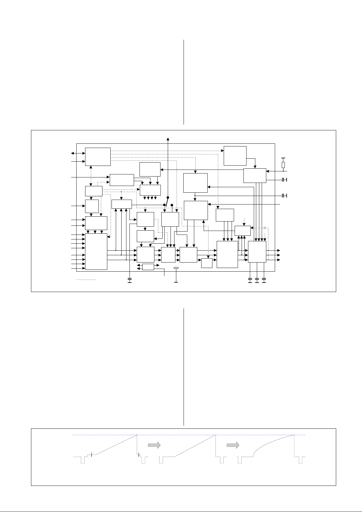
RGB Video Processor TDA4780, ICt1
g
13
Functional description
General
The TDA4780 circuit is an RGB Video Processor with an
automatic cut-off control, gamma adjustment, dynamic
black control, and blue stretch.
The IC contains a linear matrix to convert the luminance
and colour difference signals into RGB signals. The processor is also able to process two external RGB signals.
All parameters and functions are controlled using the IICbus.
Y
26
Y
(Hue)
D/A
converters
Contrast
adjust
5
+8V
SDA
SCL
Sandcastle
Y
V
U
R
G
B
Fsw
R
G
B
Fsw
28
27
14
8
7
6
10
11
12
13
2
3
4
1
2
I C-bus
interface
Control
registers
0.45V/
1.4V
VBS
PAL/SECAM
NTSC
Matrix
Fast
signal
switch,
blanking
IIC bus data
and control
TDA4780
Sandcastle
detector
Y-Matrix
R
G
B
18
1st and 2nd
switch on
delays
Timin g
generator
Timing pulses
Adaptive
black
control
Gamma
adjust
Saturation
adjust
Supply
Peak dark
storage
Signal input stages
The luminance and colour difference signals from the Feature box module are input to pins 8 (Y), 6 (U) and 7 (V). The
luminance signal input level is selectable (0.45 Vpp or 1.4
Vpp) using the IIC-bus (pins 27 and 28). 1.4 Vpp is used in
this application. The signals are fed to a linear matrix stage
to convert them into RGB signals.
RGB signals from the teletext circuit are fed to the input
pins 2 (R), 3 (G) and 4 ((B). RGB signals from the PIP module (or from the VGA connector) are fed to the input pins
10 (R), 11 (G) and 12 (B).
All input signals are clamped in order to have the same
black levels at the signal switch input.
3x6-bit
Peak drive
limiter,
6-bit D/A
converter
Brightness
adjust
9
Ground
Averag e
beam and
peak drive
limiting
R
G
Blue
stretch
reference
registers,
MUX, DAC
PDL
3x6-bit
DAC
Blanking,
measurement pulse
insertion,
white point
adjust
Cut-off
comparators
Peak
detector
Cut-off storage
Cut-of f
adjust,
output
stages
21
B
23 25
R
G
19
17
16
15
24
22
20
Leakage
and cut-off
current
input
Leakage
storage
Peak drive
limiting storage
Averag e
beam current
R
G
B
Signal switches
Fast signal source switches select RGB signals from one
of three input signal alternatives: the matrix stage, the teletext circuit or the PIP module. This selection is controlled
using the IIC-bus or by using fast blanking signals FB on
pins 1 and 13. During the vertical and horizontal blanking
time, an artificial black level is inserted in order to clip off
the sync pulse of the luminance signal, to suppress hum
during the cut-off measurement time, and to eliminate
noise during these intervals.
Y -matrix and adaptive black level, gamma and saturation controls
Saturation control is performed by varying the amplitude
of the RGB signals relative to the luminance signal amplitude. For this reason the luminance signal has to be regenerated in the Y-matrix from the RGB signals.
After the Y-matrix, the luminance signal is fed to the adaptive black level control stage. This detects the lowest volt-
Nom white
level
Nom black
level
Input si
nal Adaptive Black level Control Gamma Adjust
Principle of the adaptive black control and gamma adjust
age of the luminance component of the internal RGB signal during the scanning time and moves it to the nominal
black level. In order to keep the nominal white level constant, the contrast is increased simultaneously. The process expands the dynamic range of the contrast.
Next, the luminance signal is processed in the gamma adjustment stage. This has a non-linear transmission characteristic. The gamma adjustment stage amplifies the lower
levels of the signal using a higher gain. This process improves the separation of the dark parts of the picture from
each other. Finally the luminance signal is fed to the colour saturation control stage.
The Y-signal is fed in addition to the adaptive black level
control stage through an internal switch to the output pin
26 and onwards to the SVM module.
The gamma and saturation adjustments are controlled
using the IIC-bus.
Page 22

14
Contrast and brightness control
Both adjustment blocks consist of electronic potentiometers
and are controlled via the IIC-bus. The contrast control has
an influence on the amplitude of the RGB signals and the
brightness control on the DC level of the RGB signals relative to the black level.
Blue stretch
The blue stretch channel gives additional amplification if
the blue signal is greater than 80% of the nominal signal
amplitude. In such cases, the white point is shifted towards
a higher colour temperature so that white parts of the picture seem to be brighter.
ing generator includes a line counter which controls the
blanking and measurement pulse insertion stages.
Switch-on delay circuit
After switch on, all signals are blanked and a warm up test
pulse is fed to the outputs during the cut-off measurement
lines. If the voltage on the cut-off measurement input exceeds an internal level, the cut-off control is enabled but
the signal still remains blanked. Signal blanking is stopped
when the cut-off control has stabilized.
CRT module
Measurement pulse insertion and blanking
During the horizontal and vertical blanking time and the
measurement period, the signals are blanked to an ultra
black level, so the leakage current of the picture tube can
be measured and compensated for automatically.
Measurement pulses are generated in the timing generator and are inserted into the R channel during line 20, the
second is inserted into the G channel during line 21 and
the third is inserted into the B channel during line 22. These
measurement pulses are fed with the RGB signals to the
video output amplifiers (ICh1, ICh2 and ICh3), and feed back
the voltage levels to pin 19. During the cut-off measurement lines, the output signal levels are at the cut-off measurement level. The vertical blanking period is timed using
a sandcastle pulse. The measurement pulses are triggered
by the negative going edge of the vertical pulse of the
sandcastle pulse and start after the following horizontal
pulse.
White point adjust, automatic cut-off control and
output stages
The nominal signal amplitude can be varied ±50% by the
white point adjustment using the IIC-bus. During the leakage measurement time, leakage is compensated in order
to get a reference voltage on the cut-off measurement input pin 19. This compensation value is stored in the external capacitor on pin 17. During cut-off current measurement times for the R, G and B channels, the voltage on this
pin is compared with the reference voltage, which is individually adjustable via the IIC-bus for each colour channel.
The control voltages so derived are stored in the external
feedback capacitors on pins 21, 23 and 25. Shift stages add
these voltages to the corresponding output signals. Finally,
the RGB signals are amplified to the nominal value of 2
Vpp and the signals are output on pins 24 (R), 22 (G) and
20 (B).
Beam current and peak drive limiting
The circuit is provided with two kinds of signal limiter. An
average beam limiter, which reduces the signal level if a
certain average value is exceeded and a peak drive limiter,
which is activated if one of the RGB signals even briefly
exceeds the IIC-bus determined threshold. The beam current limiting voltage is taken from the cathode current information and fed via transistors tt4 / tt1 and capacitor Ct29
to pin 15. If the voltage on the pin 15 decreases below +4 V
due to the charge of capacitor Ct29, the internal limiter starts
to reduce the contrast. If the voltage decreases below +2.8
V, the limiter also starts to reduce the brightness.
Video output amplifiers ICh1, ICh2 and ICh3
The video output stage consists of three separate output
amplifiers, TDA6111. The circuit has a high slew rate and a
large 16 MHz bandwidth and is thus suitable for 100 Hz
applications. The circuit is protected against CRT flashovers
and electrostatic discharges (ESD).
The RGB signals from the RGB video processor are fed via
low pass filters to the inverting input pin 3 of the amplifiers. The non-inverting input pins 1 are connected to a voltage level of +3 V. The amplifiers have two outputs for the
picture tube cathodes, pin 8 for the DC currents and pin 7
for the transient currents. After these output pins the amplified RGB signals are fed to the picture tube cathodes.
The feedback information is output from pin 9 and connected via a resistor to input pin 3. Monitoring of the black
level of the cathodes is done via output pins 5. These outputs are connected together via resistors and the final result is fed to the RGB video processor, pins 19 (cut-off control) and 15 (beam current). The required supply voltages
are fed to pins 2 (+12 Vp) and 6 (+200 V).
A negative flyback pulse from the diode split transformer
Mk1 (DST) is fed to the control grid G1 via connector Xh12, capacitor Ch19, and resistor Rh28. This intensifies the
horizontal blanking during the line flyback.
The blanking of the screen after switching off is done by
transistors Th1 and th2. During normal operation, capacitor Ch27 is charged to +12 V and capacitor Ch18 to +200 V.
When the set is switched off, Ch27 discharges to the base
of Th1. The transistor conducts and discharges Ch18 as
negative charge on to the control grid G1. Also, capacitor
Ch28 is charged to +12 V and when the set is switched off,
the base of th2 goes low and the transistor conducts. Ch28
discharges to the non-inverting input pin 1 momentarily
causing about +200 V to be fed to the outputs. This prevents the increase of the beam current until Th1 has had
time to block the picture tube.
Sandcastle detector and timing generator
The two level (2.5V / 4.5V) display sandcastle pulse (DSC)
from the deflection controller on the Feature box is fed to
input pin 14. The sandcastle detector separates the
sandcastle pulse into combined line, field pulses and clamping pulses, which are fed to the timing generator. The tim-
Page 23
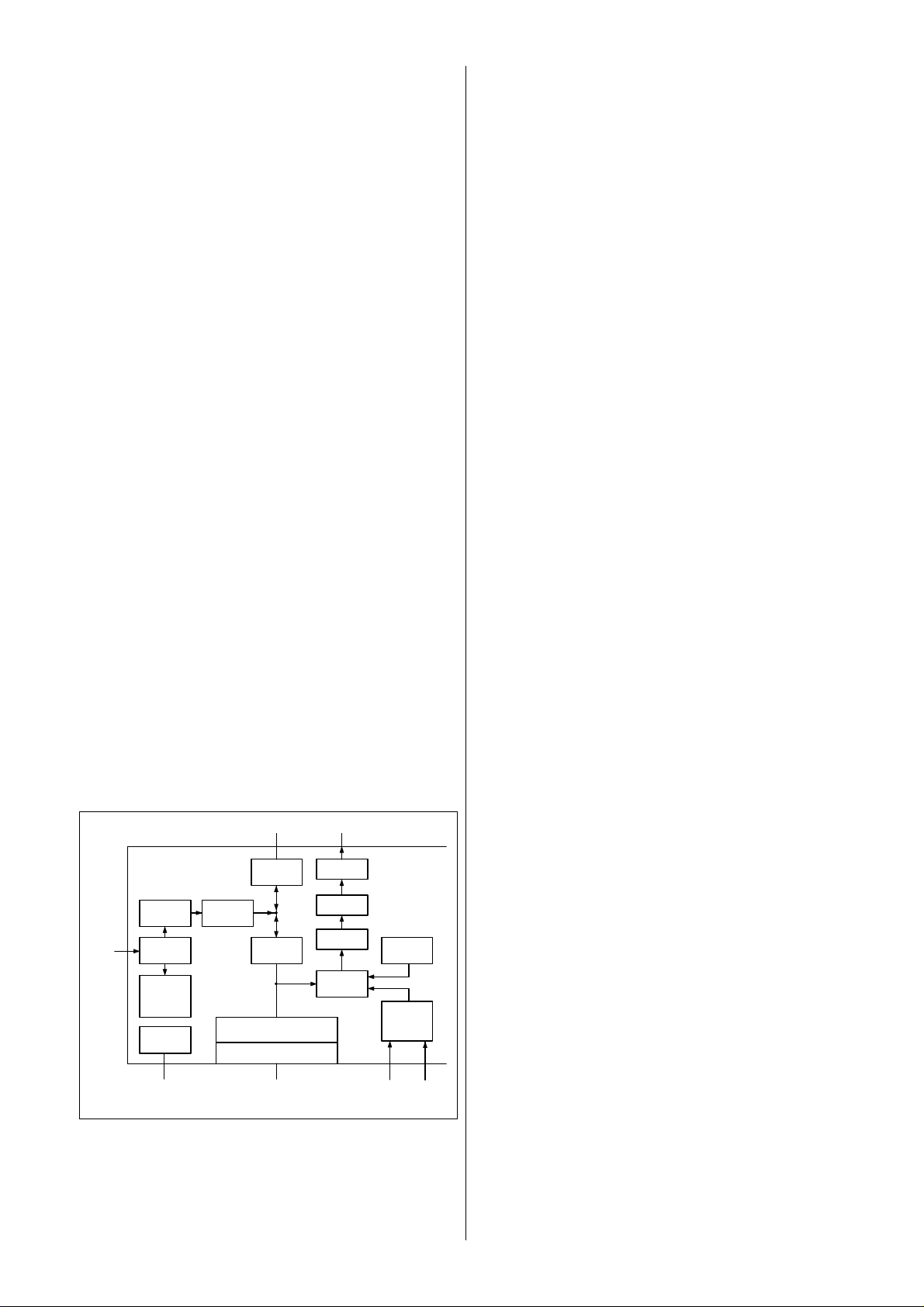
Teletext
y
Megatext SDA5273, ICr1
The SDA5273 Megatext circuit is a single chip which combines data slicer, teletext processor, page / pixel memory,
and display controller. Digital signal processing is used to
eliminate external discrete components.
The memory can be extended using an external DRAM to
increase the teletext capacity.
The multistandard capability of the Megatext circuit ensures its suitability for all countries which transmit the
World System Teletext (WST) level 1.5.
The Megatext circuit functions are the decoding and display of teletext information from an analog source, CVBS
input, and the generation of On Screen Displays, which
can provide the TV user with status information or assistance. The RGB output of the Megatext IC is connected to
the RGB input of the RGB video processor together with
fast blanking information.
The Megatext IC is controlled through the M3L-bus which
has a maximum data rate of 1 Mbit/s.
Circuit description
The CVBS signal from the video matrix switch is fed to
input pin 9.
The basic principles of the signal handling are shown in
the block diagram below.
The analog RGB signals and fast blanking signal are output on pins 44 (R), 45 (G), 46 (B) and 47 (FB). The vertical
sync pulse (2V) is fed to pin 3 and the horizontal sync pulse
(2H) to pin 4. Sync pulses are taken from the Feature box
(VDFL and HDFL).
An external 20.48 MHz crystal is connected between pins 5
and 6. Pins 18...35 and 37 are the address and data lines
for the external DRAM (icr2). The +5 Vr supply voltage is
fed to pins 10, 11, 13, 15 and 17. A high level on pin 14
causes the chip to be reset.
A stabilized 3.3 V reference voltage for internal use, from
the zener diode Zdr1, is connected to pin 16.
The Megatext circuit communicates with the
microcontroller via the M3L-bus, using pins 49 (SCL), 50
(SDA) and 51 (IICENable).
15
Data Slicer separates the teletext data from
the digitized CVBS signal.
Acquisition Interface synchronizes the bytes, con-
verts serial bits to the parallel
bytes and detects the framing
code.
Processing Unit manages the interchange func-
tions between acquisition,
memory, display, and bus inter-
face.
Internal Memory Internal 24 Kbyte DRAM.
Ext DRAM Interface Interface between the megatext
and external DRAM.
Display Generator controls data transfer from
IRAM to DG, decodes the dis-
play words, controls the display
formats and generates special
cursors.
Character ROM Character pixel memory.
CLUT Colour look up tables.
Display clock and Timing generates the horizontal timing
signals for the display and a line
locked display clock.
FIFO speeds up the pixel rate from
normally 24 MHz to 32 MHz in
16:9 mode.
D/A converter produces analog RGB signals.
Bus Interface M3L-bus interface between the
Megatext and microcontroller.
Megatext Plus SDA5275, ICr1
The Megatext Plus circuit SDA5275 is based on the original Megatext circuit SDA5273. The main difference is in
the internal data processing, which enables the teletext data
processing in accordance with the level 2.5. The level 2.5
generates much better graphics (bitmap graphics), more
colours (4096) and an extension for the 16:9 format, which
enables a wider display page. Consequently, the level 2.5
can display 56 characters on each 25 lines (1400 characters / page). The level 1.5 can display only 40 characters
per line (1000 characters / page).
Because of higher level pages, the Megatext Plus circuit
always requires an external memory circuit.
M3L-Bus RGB
CVBS
SDA 5273
Data
Slicer
A/D
Converter
Sync
Slicer &
Timing
Crystal
Oscillator
20.5 MHz
Cr
stal
Interface
Bus
Interface
Acq
PU
24-KByte DRAM
External DRAM-Interface
to external
DRAM
DAC
FIFO
CLUT
Display
Generator
Character
ROM
Display
Clock &
Timing
2V
2H
A/D Converter converts the CVBS signal to 7-
bit binary code.
Sync Slicer and Timing separates the hor/vert sync
from the digitized CVBS signal
and generates a line-locked 24
MHz acq clock.
Teletext memory DRAM, icr2
The external teletext memory is a 4 Mbit high-speed Dynamic Random Access Memory (DRAM). It is organized as
1 048 576 four-bit words (4 194 304 bit). The circuit uses
CMOS silicon gate technology.
One teletext page takes 1 Kbyte (8 192 bit) of memory, so
the circuit is able in theory to store 512 teletext pages (4
194 304 : 8 192 = 512). This reduces the page access time
to virtually zero.
During the first cycle of the teletext transmission, the
memory circuit is formatted for the transmitted pages.
During the second cycle, transmitted pages are stored in
the memory.
Page 24

16
CONTROL SYSTEM
The control system consists of the following circuits,
- Program memory, ICf1
- NV RAM, ICf2
- Microcontroller, icf3
- AND gate, icf4
- Reset circuit, icf5 and
- Remote control and local control
Program memory, ICf1
Depending on the receiver version, the chassis may be
equipped with either 4 Mbit or 8 Mbit program memory.
Both are high speed Ultraviolet erasable and Electrically
Programmable Read Only Memories (UV EPROM). Later,
also an OTP (One Time Programmable) ROM or just a ROM
can be used.
The 4 Mbit (512 kbyte) memory is organized as 524 288
eight-bit words. The microcontroller addresses this
memory using the address lines A0...A18.
The 8 Mbit (1024 kbyte) memory is organized as 1 048 576
eight-bit words. This memory needs extra banking. This is
carried out by icf4, which divides the address space into
four separate blocks, data bank 0, 1, 2, and 3. The basic
software is programmed into data banks 0 and 1. Data
banks 2 and 3 are used for the Menu text and Electrical
User Manual (EUM) text.
The program memory communicates with the
microcontroller via the address and data bus.
NV RAM, ICf2
The NV RAM is a low power CMOS, 16 kbit Electrically Erasable and Programmable Read Only Memory (EEPROM). It
is organized as eight separate address blocks, each consisting of 256 eight-bit words (8 x 256 x 8 = 16 384 bits).
Data is transferred via the IIC-bus.
Settings which can be stored in NV RAM include TV program memory location information, IIC-bus controlled service adjustments, normalization settings, user settings, option and configuration data, and teletext bank pages.
Microcontroller, icf3
The SDA30C264 is a low power CMOS circuit which includes an eight-bit CPU, a 2048 byte + 256 byte data
memory (RAM), an oscillator and clock circuits, two 16-bit
timers / counters and a watchdog timer. The microcontroller
is connected to the program memory via address and data
bus and to the other circuits via the IIC-bus.
Depending on the size of the program memory (4 Mbit or
8 Mbit) and the picture ratio (4:3 or 16:9), some components (and gate icf4 and few jumpers) are either installed
or omitted. Consequently, some microcontroller pins have
different functions.
The pins marked by an asterisk (*) are explained in more
detail after the pin configuration table.
Pin configuration of the microcontroller SDA30C264
Pin Description
1 Headphone switch input, Hp connected = high
2 AV-link data out to scart pin 10, high pulses
3 * 4Mb/4:3 : TA700 status in, plug connected = high
All 8Mb and all 16:9 : picture tilt output, 0...5 V
4 M3L-bus, enable for Megatext, enable = low
5 Hor shift adjustment in VGA sets
(PWM -> Xo3-1 = 0...5 V)
6 * 4Mb/4:3 : RGB status in, status on = high
All 8Mb and all16:9 : RGB status in = high / TA700
status in, plug connected = high
7 Hold from service connector, hold = low
8 * Bank 1 / EPROM data bank selection control (8Mb)
9 * Bank 0 / EPROM data bank selection control (8Mb)
10 Ground
11 Supply voltage, +5 Vstb
12...13 Crystal 12 MHz
14 Reset input, reset by low
15 Not connected
16...28 Address bus for program memory (EPROM)
29...36 Data bus for program memory (EPROM)
37...39 Address bus for program memory (EPROM)
40 Ground
41 Supply voltage, +5 Vstb
42 Address bus for program memory (EPROM)
43 * EPROM data bank control (8Mb). Low = data
bank 0, high = data banks 1, 2 and 3
44 IIC-bus, serial clock
45 IIC-bus, serial data
46 Rec LED on by low / Local control read pulse out
(in to pins 61 or 62)
47 * Multistandard IF = strobe pulse (low) for data latch
Non multistandard IF = APSi filter driver, APSi
by high
48 * P_on, picture on voltages by low
49 * R_on, recording voltages by low
50 * Reset pulse (high) for MSP / Subwoofer
identification = low
51 * Audio mute by high / Identification of 16:9 (lower
voltage), 4:3 (higher voltage)
52 * Scart 3 identification / status in (off = 0 - 1.2V,
16:9 = 1.3 - 3.2V, 4:3 = 3.3 - 5V)
53...54 Scart 1, 2 status in (off = 0 - 1.2V, 16:9 = 1.3 - 3.2V,
4:3 = 3.3 - 5V)
55 Version identification of IF module. Reads the
resistor R556 (multi) / R526 (non multi)
56 GND
57 Address for program memory (EPROM)
58 Reference voltage of internal D/A-converters
59 M3L-bus, clock for Megatext
60 M3L-bus, data for Megatext
61 Local control 2 input
62 Local control 1 input
63 AV-link data in from scart pin 10, low pulses
64 Remote control input, high pulses
Page 25

The list below gives more detailed information about each
pin marked *.
3 a) In 4:3 sets with 4 Mbit program memory, pin 3 inputs
status information (line out status) from the adjustable
audio module. It indicates whether the module is in use
or not, that is, whether the plug is connected or not. If
the plug is connected, transistor ta9 does not conduct
and pin 3 is high. This activates a three level mute selection: 1) TV’s speakers are muted, 2) TV’s speakers
and adjustable audio module are muted or 3) no mute.
The circuit icf4 is not installed and the link to the picture tilt adjustment is disconnected.
b) In all 16:9 and all 8 Mbit program memory sets, pin 3
outputs a picture tilt adjustment. In these cases, information from audio module is disconnected. With the
tilt adjustment the picture declination caused by the
magnetic field of the earth can be compensated for.
Depending on the control voltage, transistors tt5, tt6
and tt7 drive the voltage either from +12 Vr via the canceller coil to +5 Vr (low control voltage, tt6 conducts) or
from +5 Vr via the canceller coil to ground (high control
voltage, tt5 and tt7 conduct).
6 a) In 4:3 sets with 4 Mbit program memory, pin 6 oper-
ates as an indication of the RGB status (rf51 is installed).
If the RGB connection is in use, transistor tq4 does not
conduct and pin 6 is high.
b) In all 16:9 and all 8 Mbit program memory sets, pin 6
operates as an indication of the RGB status (= scart pin
16 high) and TA700 status via icf4 (rf51 is not installed).
The software periodically checks the status by feeding
out a high level from µC pin 9 to icf4-4 pin 13, and if
icf4-4 pin 12 is high (RGB status on), pin 11 feeds a high
level out to µC pin 6.
The same checking routine takes place for the TA700
status, but this uses µC pin 8 and icf4-3. During this
check, µC pin 43 (A18) is always low. This means that
the levels on pins 8 and 9 have no influence on the data
banking of the EPROM.
17
48 / P_on 49 / R_on Description
H H Micropower standby mode,
power supply does not operate
L L TV on mode, Vr, Vp and Vstb
available
H L Rec mode, Vr and Vstb available,
Vp not available
L H Service standby, Vstb available,
but not Vr neither Vp
The receiver is in service standby mode whenever it
has been set to service mode by pressing the -vol /
menu, TV and i buttons, but not yet switched on by
pushing the TV button twice. Service mode is indicated
by the rec LED (illuminated), as well as rec and service
standby modes.
50 a) During startup phase, pin 50 feeds out a positive
going reset pulse for the sound processor.
b) By sensing the load on the reset pulse, pin 50 detects whether or not the subwoofer is installed. If the
subwoofer is installed, resistor Ra107 is also present in
which case the amplitude of the reset pulse is smaller
than it is when Ra107 is absent. This check takes place
during the configuration phase (in service mode when
the red button is pressed).
51 a) During the configuration phase, pin 51 checks the
resistor ra10 via transistor ta10 (b-e) in order to identify
the picture tube ratio. Low resistance indicates 16:9 and
high resistance 4:3
b) During normal operation the audio amplifier can be
muted by a high level on this pin (central mute)
52 a) In the configuration phase, pin 52 checks the possi-
ble installation of a scart 3 module by checking the resistor ra26 (on the scart 3 module)
b) Pin 52 operates as a status input pin from scart 3
8/9 When µC pin 43 is high, these pins select, via icf4-1 and
icf4-2, the required data bank, either 1, 2 or 3.
When µC pin 43 is low, only data bank 0 is in use, thus
pins 8 and 9 have no influence on data banking, but
they can be used for other functions.
43 Pin 43 is an address line that is used for data banking of
the 8 Mbit program memory. When the pin is in a low
state, data bank 0 is selected, and when high, either 1,
2 or 3 are selected. For the 4 Mbit memory, pin 43 is a
normal address line (A18)
47 a) In multistandard sets, pin 47 feeds out a strobe pulse
(low) for the shift register on the IF block
b) In non multistandard sets, pin 47 drives the switching transistor T501 on the IF block. During channel
search (APSi), pin 47 is high
48/49
The combination of levels on these pins determines the
working state of the receiver as follows:
AND gate, icf4
The AND gate icf4 operates as a function expander in all
16:9 sets (4 and 8 Mbit program memory) as well as in all
sets equipped with 8 Mbit program memory (4:3 and 16:9).
In these cases, the jumpers rf30 (program memory pin 31),
rf31 (program memory pin 1), rf48 (µC pin 3) and rf51 (µC
pin 6) are not installed.
In 4:3 sets with 4 Mbit program memory, the AND gate is
not installed, but the above mentioned jumpers are installed.
For a more detailed description, refer to microcontroller
pins 6, 8, 9 and 43.
Reset circuit, icf5
The microcontroller is reset by a special reset circuit, icf5
(TL7705A). When the receiver is switched on, pin 5 feeds a
low level to pin 14 of the microcontroller until the +5 Vstb
on the monitoring pin 7 (sense) reaches a level of +4.55 V.
After that the reset continues for about 30 ms. Then pin 5
goes high and the microcontroller is reset. The reset delay
time of 30 ms is determined by capacitor Cf21 on pin 3.
If the +5 Vstb drops below the 4.55 V threshold level even
for a moment, reset takes place immediately and the
microcontroller is blocked causing the receiver to switch
to micropower standby mode.
Page 26

18
Remote control
The remote control uses the NRC-17 coding system based
on a 17-bit biphase code. The infrared receiver / amplifier
Hfc1 receives pulse modulated infrared light. The receiver
converts the light into an electrical signal, which is demodulated, amplified, and fed out from pin 3. The signal is taken
to microcontroller pin 64 via transistor tfc3. During code
transmission, the microcontroller sends negative pulses
from pin 46. This causes LED Dfc4 to flash as an indication
of the accepted code.
Local control
The local control comprises only four primary daily use
functions: volume + / - and program stepping + / -. These
functions makes it possible to use the receiver without the
hand-held remote control unit. The information from function switches SWfc1...SWfc4 is fed to microcontroller pins
61 and 62.
The LEDs on the local control unit indicate the receiver state
as follows:
In On-mode, the green LED Dfc17 lights due to the +12Vp.
In Stby-mode, the red LED Dfc16 (on the micropower block)
lights to indicate the mains voltage is connected.
In Rec-mode, the red LED Dfc4 lights due to the low level
on microcontroller pin 46.
Page 27
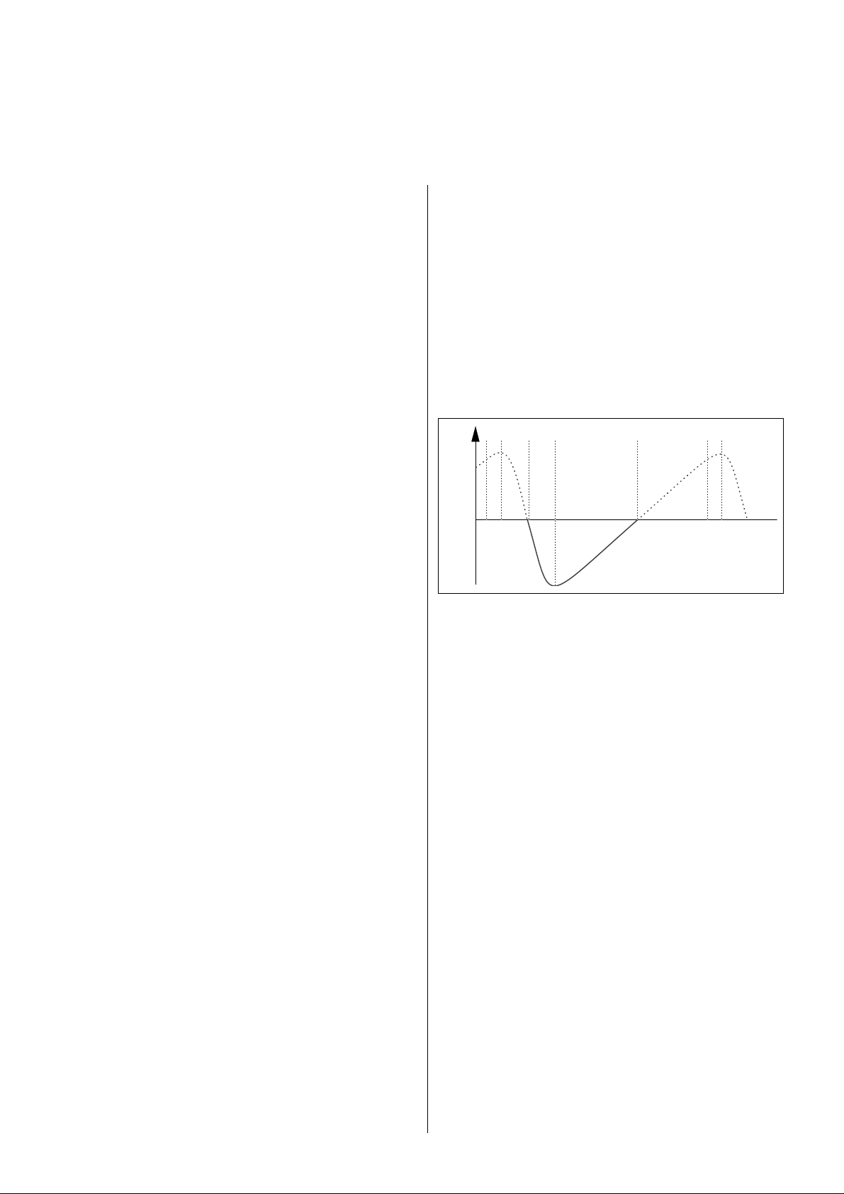
DEFLECTION STAGES
- Vertical deflection
- Horizontal deflection
19
Vertical deflection
The TDA8354 is a DC-coupled Vertical Deflection output
circuit containing an internal vertical flyback generator and
a guard circuit. The output amplifiers and flyback generator are fitted with power FETs. The IC is thermally protected
and in addition it is protected against short circuits between
the outputs and from the output pin to ground and to the
supply voltage.
Functional description
Symmetrical vertical pulses from the deflection processor
TDA9151 are fed via pins 11 and 12 to a current driven
differential input circuit. The current to voltage conversion
is carried out by resistor rs4 via input pin 3. The voltage on
pin 3 is compared with the feedback information on pin 2.
The feedback information is taken from the output current
through the deflection coil measured across resistors Rs2,
Rs3 and Rs5.
The signals are amplified using a vertical driver circuit in a
bridge configuration.
The deflection coil is connected between the phase opposition driven amplifiers at output pins 5 and 9. The output
current is determined by the value of resistor rs4. The resistor network (VD6xx), connected in parallel with the deflection coil, damps down the high frequency oscillation
which tends to be generated at the end of the flyback period. Resistor rs6 on pin 13 is added to compensate for the
current differences in the dumping resistors during the scan
and flyback period.
The operating supply voltage of +16 V on pins 4 and 10,
and the flyback supply voltage of +50 V on pin 7 are taken
from the diode split transformer Mk1. Operation with two
supply voltages (class G) makes it possible to set both supply voltages independently to their optimum values. In this
way a very high efficiency is achieved. Due to the bridge
configuration, a decoupling capacitor is not necessary. Thus
almost the whole flyback supply voltage is available across
the deflection coil.
The output of an internal guard circuit is connected to pin
1. The sandcastle pulse (DSC) from the deflection processor is also connected to the same pin.
The guard circuit is activated in possible fault situations,
such as short circuits at output pins, an open deflection
loop, or circuit overheating. In such cases the guard circuit
increases the DC level on pin 1 to 2.5 V. This is the same
DC level as the blanking level of the sandcastle pulse. This
causes blanking of the screen that protects the picture tube.
Horizontal deflection
The horizontal drive signal from the deflection processor
is fed to the driver transformer Mk2 via a pulse shaping
network consisting of transistors tk6, Tk1, Tk2, and associated components. The circuit Dk5, Rk30 and Ck17 limits
the switching transients of Tk2. The +17 V supply voltage
for the transformer is taken from the power supply. The
secondary winding of the transformer is connected to the
base of the line output transistor Tk3, which drives the diode split transformer Mk1 and the line output stage.
The functional description of the line output stage starts
from the time t5 when the drive signal becomes negative,
the line scan period is stopped and the line flyback period
t1 starts (picture below).
t5
t2 t4 t5 t1t3Iscan
t1
Line flyback (t1...t3)
Due to the cut off of the Tk3 collector current, the energy
stored in the deflection coil at the end of the scan period
flows to flyback capacitor Ck24. The energy flow continues until time t2, when all energy has been transferred and
the collector voltage reaches its maximum value. The current then changes direction and energy from the capacitor
flows back to the deflection coil. At time t3 the flyback capacitor is discharged and the voltage across it is 0 V. It
then becomes negative as the deflection coil starts the scan
period by feeding its energy to capacitor Ck27 (and Ck33).
Line scan (t3...t5)
At time t3, when the deflection coil starts to feed its energy
to Ck27, current begins to flow via diode Dk7. At time t4,
which is the mid point of the line scan, the drive pulse on
the base of Tk3 becomes positive again and the deflection
current can flow via transistor Tk3 and diode Dk8. From
time t4 to t1, the deflection current changes direction and
energy moves from Ck27 into the deflection coil. At time
t5, that is the end of line scan, the drive signal of Tk3 becomes negative and the flyback period begins again.
To achieve continuous operation, the energy from the
power supply is stored in the primary winding of Mk1 (pins
6 and 3) during the scan period when Tk3 is saturated. Some
of this energy is used to compensate for the deflection
losses.
Deflection corrections
The parabolic E-W correction pulse from the deflection
processor is fed through transistors ts1 and ts2 to the base
of transistor Tk4, which drives the E-W correction circuit
consisting of capacitors Ck26, Ck28, diode Dk8 and bridge
transformer Mk3.
Page 28
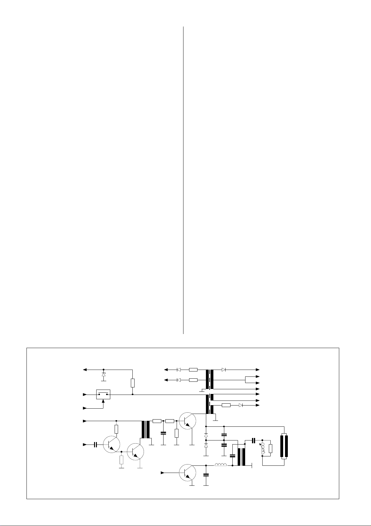
20
n
The picture width, and E-W correction adjustments (parabola, corner and trapezium) are carried out by modulating the current across coil Lk1.
The circuit Ck38, Dk9, Rk49 and Rk52 in parallel with Scorrection capacitor Ck27 eliminates the so-called “mouse
tooth” phenomena.
Dynamic focus, FO600
A dynamic focus adjustment is used in addition to the normal focus adjustment. The dynamic focus improves the
focus on both sides of the screen. In order to have a higher
focus voltage at the beginning and end of the scan period,
an auxiliary voltage is needed. This voltage is taken from a
transformer, which is connected in series with the horizontal deflection coil. The parabolic voltage across the transformer is fed via a capacitor to the dynamic focus
potentiometer and onwards to a discrete focus grid. The
dynamic focus is used only in larger picture tubes.
Horizontal scan shift and dynamic focus, FO7xx
Receivers with a VGA connection (Feature box DB700) are
equipped with a special FO7xx module which includes a
horizontal scan shift adjustment, and also, when needed,
dynamic focus.
The horizontal shift control voltage (0...+5 V) is taken from
microcontroller pin 5 to the module connector Xfo3-1. The
connector Xfo3-2 is connected to +12 Vp.
When the control voltage is low, transistor tfo5 conducts.
Due to resistors rfo4, rfo5 and rfo6 the base voltage on
transistors tfo3 and tfo4 is low, causing tfo3 and Tfo1 to
conduct. Diode Dfo2 conducts and capacitor Cfo7 is charged
to the positive voltage, which is fed onward to the deflection path via resistor Rfo2 and transformer pins 2 and 4.
When the control voltage is high, transistor tfo5 is switched
off and resistors rfo4 and rfo5 are not in parallel connection with rfo6. This means that the voltage level on the
bases of tfo3 and tfo4 is high, causing tfo4 and Tfo2 to
conduct. Diode Dfo1 conducts and capacitor Cfo6 is charged
to the negative voltage, which is fed to the deflection path.
By varying the control voltage between 0 and 5V, the deflection path can be made more negative or more positive,
and thus the horizontal scanning can be shifted sideways.
Capacitors Cfo2 and Cfo3 operate as S-correction capacitors. This means that in VGA sets, the original S-correction capacitors (Ck27 and Ck33) on the main board are short
circuited.
Capacitor Cfo4 and coils Lfo1 and Lfo2 apply an additional
correction to the linearity.
Diode split transformer Mk1
The primary winding (pin 6) of the diode split transformer
(DST) is connected to the +130 V supply voltage via FET
switch Tsw1. In order to protect the switching transistor in
the power supply, power consumption will be reduced
during the switch off phase by the FET. During normal operation, the FET conducts due to a high level on the gate.
When the TV set is switched off, the +12 Vp drops and transistor Tsw2 conducts. Capacitor Csw1 discharges through
transistor Tsw3, which conducts and grounds the gate causing the FET to switch off.
The DST produces the flyback pulses from the primary
winding (pins 6-3) to the secondary windings and generates the following voltages:
- High voltage (30kV) for the picture tube anode
- Focus and screen grid (Ug2) for picture tube
- Filament voltages for the picture tube cathode from pins
10-11
- +200 V for the video output amplifiers from pins 12-4.
This voltage is rectified by diode Dk1
- +50 V from pins 1-5 or +46 V from pins 2-5 for the vertical
IC. This voltage is rectified by diode Dk2
- +16 V for the vertical IC from pins 7-5. This voltage is rectified by diode Dk3
- EHT information from pin 8 (and Ck21)
+30 V
U1
+12 Vp
+17 V
Hor
drive
ZDk1
Tsw1
Tk1
Rk11-14
Tk2
Mk2
+53 V
+16 V
E-W
drive
Dk2
Rk9
Dk3 Rk19
Tk3
Tk4
Mk1
Dk7
Dk8
Ck26
Ck28
Lk1
Rk2 Dk1
Ck24
Mk3
Ck27/33
Lk2
EHT 30 kV
Focus
Ug2
EHT compensatio
Filament 6.3 V
+200 V
Defl
coil
Page 29

OPTIONS
Active Subwoofer
Comb Filter CF700
SVM module
Audio Feature AR700
Audio Feature AR701
Adjustable Audio TA700
Scart 3 + VGA-audio TA710
Scart 3 TA711
Picture in Picture PP700 / 710
Active Subwoofer
21
General
The active subwoofer system provides a clear improvement in stereo sound. The system consists of active filters,
power amplifiers, a subwoofer, and stereo speakers. The
active subwoofer stage is designed to be used with an internal subwoofer box and stereo speakers in the TV set or
with small external front speakers.
Functional description
The left and right stereo channels are already added together in the sound processor MSP3410D. The sound processor also includes the required lowpass filters for the
subwoofer channel and highpass filters for the loudspeaker
channels.
The signal is taken from sound processor pin 31 and fed
onward to the high pass filter (40 Hz), consisting of transistor ta6 and associated components.
The filtered signal is then fed to the audio power amplifier,
ICa4. The amplifier can be muted by pulling pin 2 low. The
mute control signal is taken from microcontroller (pin 51)
via transistors ta10, ta4 and ta5. This mute function mutes
each of the audio power amplifiers in the set. However,
the subwoofer amplifier can also be muted separately. This
can be done via the audio processor. A high level on pin 5
drives transistor ta5 to conduct, which just mutes the
subwoofer amplifier. Due to the resistor network ra106,
ra105 and ra14, the central mute will be not activated in
this case.
The amplifier operates in a bridge configuration. The outputs are internally inverse feedback connected to the inputs of each other. The amplified, phase opposition signals are output from pins 4 and 6 to the subwoofer speaker.
Comb Filter module, CF700
Functional description
Depending on the standard, the module either bypasses
or filters the input signal as follows:
PAL and NTSC 3.58
The signal is fed to comb filter IC and separated
for Y and C signals
NTSC 4.43 and SECAM
The signal is fed to comb filter IC, but it is not separated
S-VHS The signal is bypassed in the multiplexer IC
The standard is identified in the colour decoder Icd1. The
standard information is input to the microcontroller via the
IIC-bus and back to the colour decoder again. The information is output from pin 23 to comb filter module pin 1,
from pin 16 to module pin 2, and from pin 15 to module
pin 13.
Module pin 1 controls the multiplexer to bypass the video
signal (“L”) or to feed the signal to the comb filter IC (“H”).
When pin 1 is high, it inputs the colour subcarrier frequency
(Fsc) to an internal clock generator of the comb filter IC.
Module pin 2 defines the comb filtering method, PAL (“L”)
or NTSC 3.58 (“H”).
Module pin 13 drives the comb filter IC to be in comb filtering mode (“H”), at which time the IC performs Y / C separation. Or to be in a bypass mode (“L”), whereat the signal
is not separated, but fed only via an internal delay stage.
In addition, pin 13 informs the colour decoder the existence of the module by transistor tc3 (base-collector joint).
Depending on which standard is in use, the logical high /
low level combinations are as follows:
General
The basic function of the comb filter is to separate the luminance (Y) and chrominance (C) signals from the CVBS
signal. The device minimizes problems caused during Y /
C separation such as dot-crawl and cross colour interference. In addition, it allows the input video signal to have
an extended frequency bandwidth. This is carried out using a clock frequency of four times the colour subcarrier
frequency. The filter is capable of handling signals according to the PAL and NTSC 3.58 standards. The module contains two ICs, the multiplexer circuit, icc1 and the comb
filter circuit, icc2.
Standard module module module
pin 1 pin 2 pin 13
PAL “H“ + 4.43 “L” “H“
NTSC 3.58 “H“ + 3.58 “H“ “H“
NTSC 4.43 “H“ + 4.43 “L” “L”
SECAM “H“ + 4.28 “L” “L”
S-VHS “L” “L” “L”
Page 30
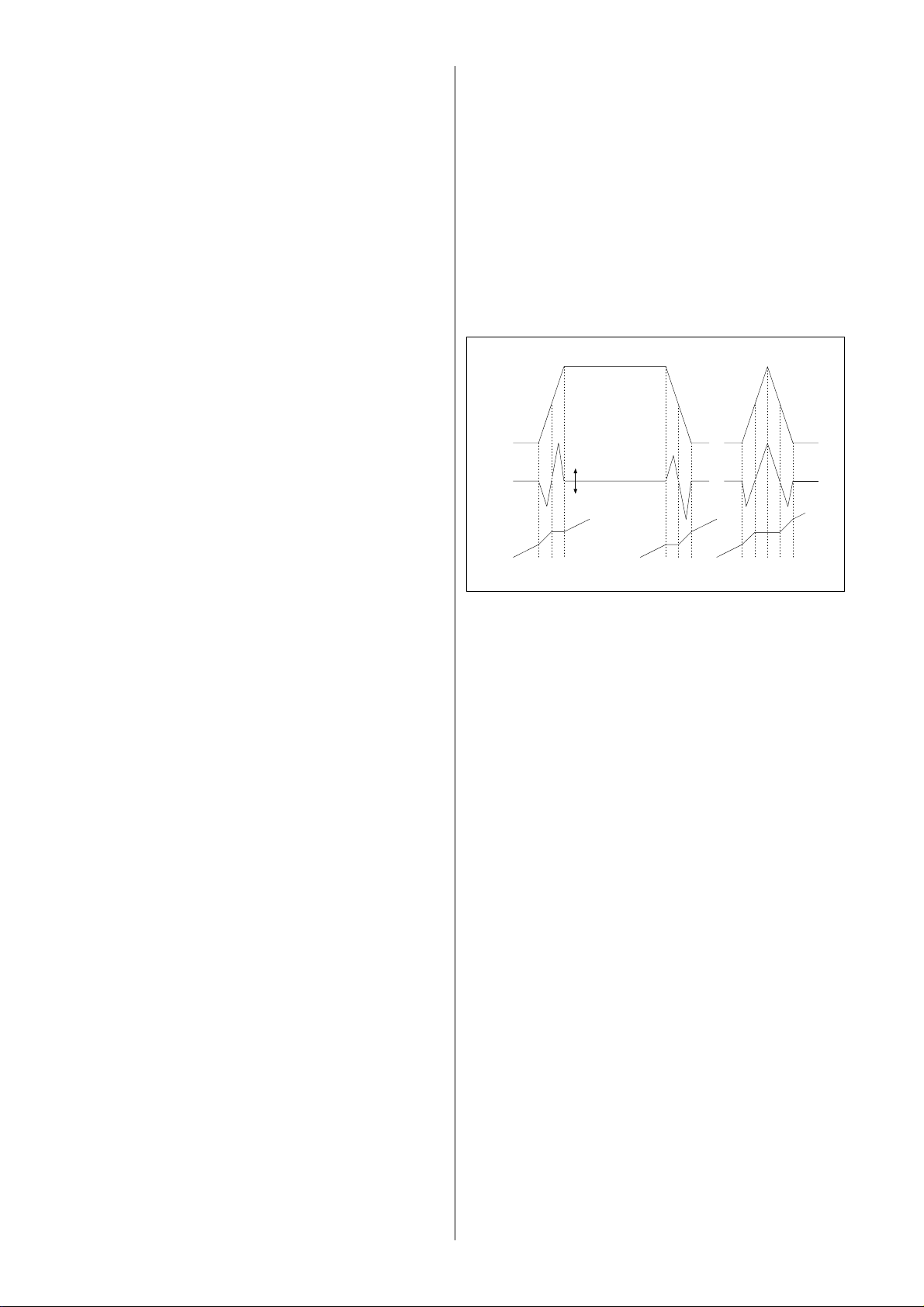
22
PAL signal
The PAL CVBS signal from module pin 6 is input to multiplexer pin 4. Due to the low level on control pin 9 (note
inverter tc10), the signal is output from pin 5, and onward
via an amplifier stage tc7 / tc8 to a low pass filter. After the
LPF and buffer transistor tc9, the signal is input to pin 15 of
the comb filter IC.
In the comb filter IC, the composite video is clamped to an
internal level and then converted by a high speed 8-bit A/D
converter. The conversion frequency is four times the colour subcarrier frequency. Due to the PAL standard, the Fsc
on pin 45 is 4.43 MHz, thus the conversion frequency is
17.7 MHz.
A logical low on pin 41 drives the video data in to the comb
filter processing block and a logical low on pin 47 defines
the filtering method in accordance with the PAL standard.
The separate luminance and chrominance signal data is
then converted into analog form by two 8-bit D/A converters. The conversion is carried out using the same clock
frequency of 17.7 MHz.
The luminance signal is output from pin 6, via the emitter
follower tc11 into multiplexer pin 12, out from pin 14, and
then on through the emitter follower tc6 to the module
output pin 10.
The chrominance signal is output from pin 8, via tc12 into
multiplexer pin 2 and output from pin 15, and then on
through tc4 to module output pin 11.
NTSC 3.58 signal
The signal routes are exactly the same as the PAL signal
routes. The only difference takes place in the comb filtering system inside the comb filter IC. Pin 47 is high, thus a
different filtering method is selected. The conversion frequency is now 14.3 MHz due to the Fsc of 3.58 MHz on pin
45.
NTSC 4.43 and SECAM signals
The signal route to the comb filter IC is the same as above.
However, now pin 41 is high and thus the comb filter IC is
in bypass mode. The signal is fed only via the A/D converter, memory block and D/A converter. The conversion
frequencies are 17.7 MHz (NTSC) and 17.1 MHz (SECAM).
The NTSC 4.43 and SECAM signals are fed via the comb
filter IC because the internal memory block imposes a two
line delay on the signal. If these signals were already bypassed in the multiplexer and the received standard
changed, for example, from SECAM to PAL, a momentary
loss of sync would occur.
Scan Velocity Modulation module, VM600
General
The purpose of the Scan Velocity Modulation (SVM) module is to increase the sharpness of the picture during intensity transients of the luminance signal.
The scan velocity modulation is carried out so that the luminance signal (a), which contains intensity transients, is
first differentiated and then amplified (b).
In this way the signal produced is fed to an auxiliary coil,
which is situated at the neck of picture tube. The current
which flows through the SVM coil during intensity transients modulates the deflection field (c), and thus either
speeds up or slows down the scan velocity.
White
Luminance
signal
Black
SVM
signal
Deflection
Chess pattern
Scan velocity slower
Scan velocity faster
Basic principle of Scan Velocity Modulation
The luminance signal is first derived by two consecutive
differentiators consisting of cvm2/rvm2 and cvm1/rvm1/
rvm3.
The derived signal is preamplified by transistors tvm1 and
tvm2, and then fed to the limiter stage, which consists of a
differential amplifier, transistors tvm3 and tvm4.
The limited signal is then fed via a driver stage (tvm6 and
tvm7) to transistors Tvm8 and Tvm9, which form the output stage, and onwards to the SVM coil.
Grid pattern
a)
b)
c)
S-VHS signal
The S-VHS signal is input to module pins 6 (Y) and 7 (C)
and onward to the multiplexer, pins 4 and 1. Pin 1 of the
module is now low, and this causes control pin 9 to go
high, and the internal switches of the multiplexer change
to bypass mode. The luminance signal is output from pin
14 and chrominance signal from pin 15.
If the transmission is a pure monochrome signal or pure
noise, meaning that there is no burst, the signal is bypassed
like an S-VHS signal. This is because there is then no colour subcarrier which is needed in the signal processing.
Page 31
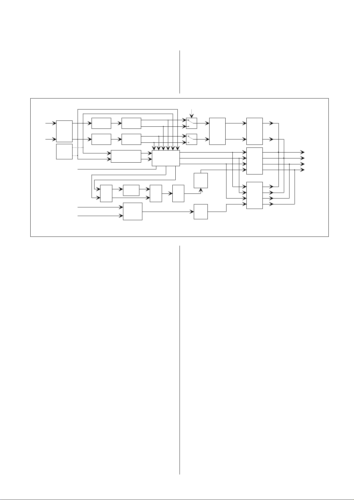
Audio Feature modules, AR700 and AR701
23
General
The audio feature module AR700 is based on the so-called
3D-audio system, which covers the audio systems called
3D Mono, 3D Stereo and 3D Movie systems.
The audio feature module AR701 consists not only the
above mentioned systems, but also the Dolby Surround
Pro Logic system.
R
L
L
L
Input
Balance
R
Noise
Generator
Bass &
Treble
Bass &
Treble
Equ Control
_GLE_GE
L
R
_GLE_GE
Graphical
Equalizer
Graphical
Equalizer
L
Adaptive
R
Matrix
S_ Equ (from
S_ Orig (from L/R)
7kHz
LPF
GLE / GE
Dolby B
Level
Echoing
for 3D
Mono
GLE
L
GE
R
GLE
R
GE
Combining
Network
)
Dolby
B
Signal process in the DSP
Both systems are produced using digital sound processing, whose program consists of seven main blocks: Dolby
Pro Logic, 3D Mono, 3D Stereo, 3D Movie, graphic equalizer, tone control, and noise generator.
Equ Control
L
3D
Stereo
L
R
C
3D
Movie
on/off
Delay
3D
Mono
on/off
Volume
ST
Stereo
Volume
DPL
Volume
ST Surround
R
L
R
C
S
L
R
C
S
L
R
C
S
Principle of the signal process in the DSP
Dolby Surround Pro Logic
The Dolby Surround Pro Logic is a four channel surround
sound system.
In the transmission phase, the four channel information is
encoded into two channels (L’ and R’). The center (C) and
the surround (S) channels are added to the left (L) and right
(R) channels according to the following formula:
- L’ = L + C x (-3 dB) + S x (-3 dB)
- R’ = R + C x (-3 dB) - S x (-3 dB)
The center channel information is added to the L and R
channels in the same phase using a factor of 0.7. The surround channel information is added to the L and R channels using the same factor of 0.7, but in the opposite phase,
as +90° into the L channel and -90° into the R channel.
In the receiver, the Dolby Pro Logic decoder decodes the
two channels, L’ and R’, back to four separate channels,
left, center, right and surround. If the transmission includes
Dolby Pro Logic sound, the software automatically switches
the receiver to Pro Logic mode, assuming that the receiver
is in AUTO mode, the transmission is in stereo (Nicam or
A2) and the WSS (Wide Screen Signalling) data includes
the Dolby bit. In addition, the rear speakers have to be connected, otherwise the software selects 3D Movie mode.
During digital signal processing, the audio data (L’ and R’)
is first fed to the input balance control, which compensates
for possible errors in the level between the two input signals. The balance control is designed to operate automatically, which is a very user-friendly feature. The automatic
system continuously analyzes the level difference between
the left and right channels and tries to keep it as small as
possible.
Next the signal is fed to the adaptive matrix stage, whose
first block is a bandpass filter. The highpass frequency of
this filter is 200 Hz and the lowpass frequency is 5 kHz.
After bandpass filtering the data (Lbp and Rbp) is fed to a
calculation block, which generates the center and surround
channels. The calculation formula is Cbp = Lbp + Rbp and
Sbp = Lbp - Rbp.
The absolute values are then taken from the Lbp, Rbp, Cbp
and Sbp signals. The next step is to calculate the relationship between the L and R channels, and also between the
C and S channels.
Next comes the time constant calculation. In the Dolby Pro
Logic decoder, there are two time constant filters. The signal level determines which one is chosen. If the level difference between L and R channels or between C and S
channels is more than 5.5 dB, then long time constant filtering is performed. After that, the short time constant filter is calculated. If the level difference is less than 5.5 dB in
both directions, then only short time constant filtering is
performed.
Finally the LR and CS signals are fed through a polarity
definition block, the last operation block in the adaptive
matrix stage, to the combining network stage.
After the combining network stage, only surround channel processing continues. In the surround channel there is
a 7 kHz low pass filter, a delay and a modified Dolby-B decoder. The lowpass filter is simply a second order filter
whose cut-off frequency is 7 kHz. The delay can be a variable delay from 15 ms to 30 ms or a constant 20 ms delay.
The modified Dolby-B decoder is a complex part of the
processing. The gain of the Dolby-B filter is dependent on
the frequency of the input signal and also on the level of
the input signal. The program uses a surround channel signal calculated without graphic (GE) and loudspeaker (GLE)
Page 32
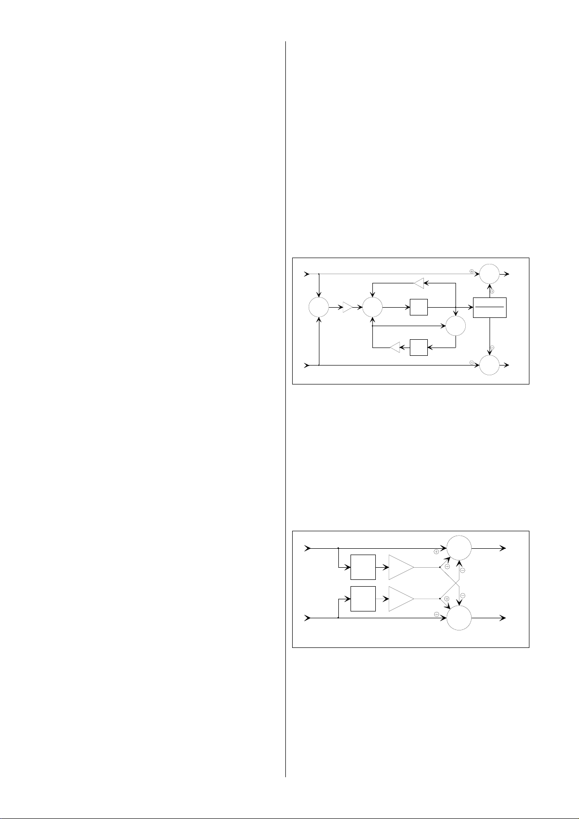
24
p
equalization for the Dolby-B level and frequency calculations. Dolby-B filtering is performed on the equalized signal.
In the Dolby Pro Logic decoder, there are 3 different center
channel modes: wide, normal and phantom.
Wide mode
If all three front speakers are capable of reproducing low
bass frequencies and they have enough amplification
power, then the system can be in wide mode. Wide is an
abbreviation of wideband, which means the whole frequency band is reproduced from the center speaker.
Normal mode
If two full range loudspeakers for the L and R channels are
available, the easiest way to set-up the Dolby Pro Logic
system is to add a small center channel speaker somewhere
near the television screen. The small loudspeakers are
normally incapable of reproducing low bass information.
In normal mode the center channel response is limited to
100 Hz and the bass content is redirected to the L and R
channels (or alternatively to the subwoofer). Another name
for this mode is “bass splitting mode”.
Phantom mode
If there is no center channel speaker available, then the
decoder can be set to phantom mode. In this mode, all
center channel information is added to the left and right
speakers.
For the surround channel there are two modes: normal and
3 stereo.
In 3 stereo mode, the surround output is cleared. The surround information is ignored and not added to the other
channels.
To summarise, there are, in principle, four different loudspeaker configurations.
Full configuration (5 loudspeakers)
- organised as two external front speakers (L / R), center
speaker, and two external rear speakers
Phantom mode (4 loudspeakers)
- where the TV’s own loudspeakers (L / R) operate as front
speakers, with no center speaker, and two external rear
speakers
3 stereo (3 loudspeakers)
- with two external front speakers (L / R), center speaker,
but no rear speakers
Basic configuration (2 loudspeakers)
- where only the TV’s own loudspeakers (L / R) are used.
In configurations where the center speaker is used, it can
be either an external speaker or the TV’s own loudspeakers connected in series. A subwoofer can be used in addition to the above loudspeakers.
The Dolby Surround Pro Logic system consists of a clock
oscillator icar1, digital sound processor icar2, delay
memory icar3, phase locked loop icar4, reconstruction filtering / digital to analog conversion icar5 and icar6, power
amplifier ICar7 and loudspeaker selection switch SWA1.
The artificial surround effect is created from the mono signal. The effect is mainly an echoing, where the size of the
space can be artificially changed by the delay control and
the richness by the effect control.
The 3D mono system is also called the 3D pseudo or SemiTech surround system.
The signal is taken from the graphic equalizers and fed to
the attenuation block to avoid an overflow. The coefficient
stage 1 and delay buffer 2 have constant values. The multiplication value is 0.12 and the delay time is limited, due
to the size of the delay memory, to 104 ms. The control
range for delay buffer 1 is between 50 ms and 150 ms and
the multiplication value of coefficient stage 2 is between
0.1 and 0.2. In the sound menu these controls are called
effect and delay.
Finally, the multiplied and delayed signal is fed to the HRTF
(Head Related Transfer Functions) filter, which artificially
shifts the audible image of the loudspeaker from its physical placement to another location.
L
coef 1
++
-18dB
R
Principle of the 3D Mono system
-1
Z
delay 1
-1
Z
delay 2coef 2
1
H + H
Left
+
i
c
++Right
3D Stereo
3D Stereo is an artificial system which is used to widen the
stereo image of the TV’s loudspeakers, thus rendering external speakers unnecessary. 3D Stereo mode only emphasizes the stereo information (no delays or echoing), thus
the 3D Stereo has no effect on a non-stereo transmission.
The effect control in the sound menu changes the amount
of emphasis on the stereo information.
The algorithm is based on a band reject filter (BRF). The
output of this filter is multiplied by an adjustable coefficient. This signal is then added to the original channel and
subtracted from the other channel
L
BRF
Adj
+
Left
coef
BRF
Adj
coef
R
le of the 3D Stereo system
Princi
+
Right
3D Mono
The 3D Mono system is designed for mono transmissions.
It is an artificial surround sound system, that creates the
surround signal from the mono signal (or from the sum of
the left and right channels) after the graphic equalizers.
This mode is suitable for non Dolby Pro Logic programmes
when a surround channel is still desired. 3D mono mode
requires no external speakers.
Page 33
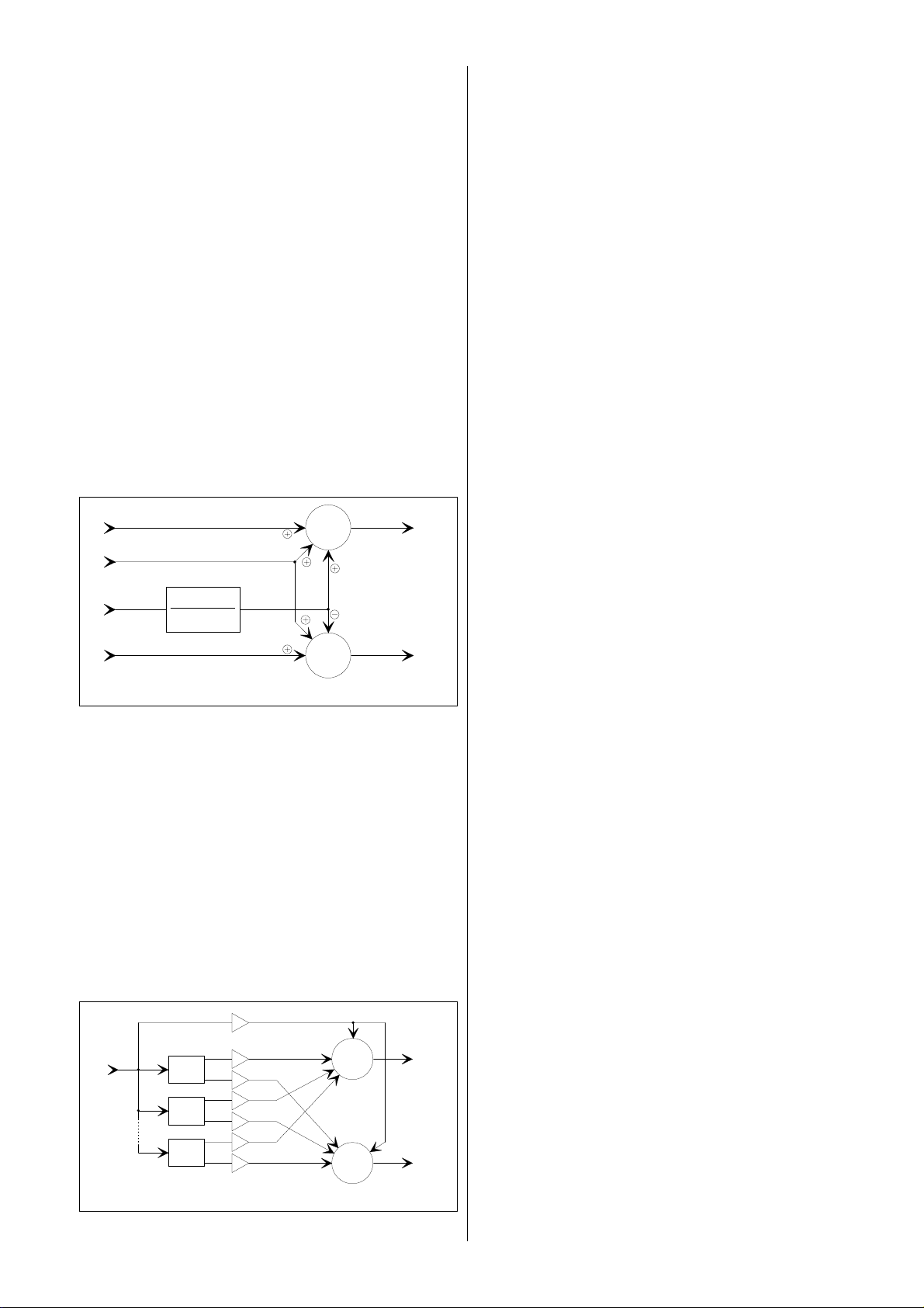
3D Movie
3D Movie is a certain kind of virtual surround sound system. With this system, some more loudspeakers can be
virtually created without installing any physical loudspeakers. Thus only the TV’s own loudspeakers are needed to
create a movie theatre sound experience. The three dimensional effect is created artificially by changing the frequency
response so that the sound appears to come from a different direction than that in which the loudspeaker is actually
situated.
The filters in the system are based on Head Related Transfer Functions (HRTF). 3D Movie requires a Dolby Pro Logic
encoded transmission in order to operate correctly. This is
because the system uses the center and surround channels in addition to the left and right channels. 3D Movie
operates only in phantom mode. This means that the center
channel is added to the left and right channels. The effect
control in the sound menu corresponds to the level control of the surround channel in the Dolby Pro Logic system.
When the transmission includes Dolby Pro Logic encoded
sound and the receiver is in AUTO mode, the software automatically changes the receiver to 3D Movie mode, assuming that the transmission is in stereo (Nicam or A2)
and the WSS data includes the required Dolby bit.
25
Tone control
The tone control stages, bass and treble, are not controllable separately as bass and treble controls, but they operate as a loudness control. This means that the tone control
is dependant on the volume control.
Noise generator
The noise generator program is used to set the channel
levels equal. Normally, the user needs this program only
during placement of the loudspeakers. The noise generator feeds the noise sample to each connected loudspeaker
channel in turn. This helps to adjust the relative balance
between the separate left, right, center and rear level settings with respect to the listeners.
L
+
Left
C
S
R
1
H + H
i
c
+
Right
Principle of the 3D Movie system
Graphic equalizer
In the digital sound processor there is a seven band graphic
equalizer for user adjustment and a loudspeaker frequency
response correction. Each of the seven bands (only three
are drawn in the principle diagram below) have two outputs. The channels, which have loudspeaker frequency response equalization, have loudspeaker equalization and
user defined gains (gGLE). The channels without loudspeaker equalization only have user defined gains (gGE).
In the sound menu, there are four different pre-set choices:
Music, Speech, Flat and Preferred. In the Music, Speech
and Flat modes, the equalizer takes the pre-settings from
the NV RAM. In Flat mode, the equalizer settings are fixed
at the middle position. Only in Preferred mode can the user
change the settings.
Xin
dir
g
GLE
H (z)
H (z)
H (z)
g
GE
g
GLE
g
GE
g
GLE
g
GE
g
Principle of the Graphical Equalizer
X
+
+
GLE
X
GE
Page 34
26
Delay memory
icar3
Signal
processor
icar2
Master
clock
icar1
PLL
icar4
DAC
icar5
Power
amplifier
ICa1
IIS-bus
Audio data
IIC-bus
Control
Reset
Mute
AR700
Block diagramme of the 3-audio (AR700) and 3D + Dolby Pro Logic module (AR701)
Functional description of the circuits
The audio feature module AR700 consists only of a clock
oscillator, sound processor and delay memory.
The audio feature module AR701 consists of, in addition
to the above, a phase locked loop, reconstruction filtering,
D/A-converter and power amplifier.
Clock oscillator, icar1
The inverter circuit icar1 operates as a master clock oscillator whose frequency of 25 MHz is determined by resistor
rar1 and capacitor car1. The clock pulses are output from
pin 8 to the sound processor pin 14.
Sound processor, icar2
The digital sound processor (DSP) includes several different memories, namely a 512 x 32-bit program RAM, 256 x
24-bit data RAM, 256 x 24-bit coefficient RAM, 1.5 kilo word
x 32-bit program ROM and 1.5 kilo word x 24-bit coefficient ROM. In addition it includes a 24-bit arithmetic logic
unit (ALU) and 25-bit x 25-bit multiplier accumulator (MAC).
In addition the circuit includes a graphic equalizer, tone
control and noise generator.
The circuit is controlled by the IIC-bus. The control software is stored in the program memory (ICf1), from which
it is sent to the microcontroller (icf3) and onward via the
IIC-bus to the sound processor. All presets are stored in
the NV RAM (ICf2). In order to ensure the proper function
of the IIC-bus during switch on and off, both the SDA and
SCL are taken to the sound processor via the +12 Vp voltage driven FETs, tar1 and tar2.
The DSP is connected to the MSP (ICa2) via the IIS-bus
which consists of four lines, data in (IIS-DI), data out (IISDO), word select (IIS-WS) and clock (IIS-CLK). The word
select signal is a 32 kHz square wave pulse and it is used
for channel separation. The clock signal is a 1.024 MHz sine
wave pulse and is used as a system clock.
Delay memory, icar3
The delay memory is a 256 kbit (32k x 8) SRAM which together with the DSP is used to create the echoing effects
needed in the Dolby Pro Logic, 3D Mono and 3D Movie
systems.
AR701
Reconstruction
filter
icar6
Equalizer control
R
L
Power
amplifier
ICar7
L&R / center
speaker switch
SWA1
LR
To surround
speakers
To external
center speaker
To internal
speakers
To external
L/R speakers
Phase locked loop, icar4
The PLL circuit generates the master clock signal for the D/
A converter. The loop is locked to the IIS-WS signal (pin 1)
that operates as a 32 kHz system clock. The PLL multiplies
the 32 kHz signal by 384 resulting in the final master clock
signal of 12.288 MHz, output from pin 10.
Reconstruction filtering and D/A-conversion, icar5
and icar6
The reconstruction filtering and D/A-conversion is carried
out using two circuits, the D/A-converter with a digital filter, icar5 (TC9270), and the filter circuit, icar6 (TA2009F).
The TC9270 includes a serial input interface, de-emphasis,
interpolators, delta-sigma modulators and D/A-converters.
The audio data is input to pin 25, and output from pins 9 /
10 (surround) and 5 / 6 (center). The whole process is controlled by three clock signals, the 1.024 MHz system clock
on pin 2, the 32 kHz word select signal on pin 3 and the
master clock on pin 4. Analog audio signals are then fed to
the lowpass filter circuit TAA2009, which performs the post
filtering. The surround channel is output from pin 6 and
center channel from pin 3 to the power amplifier.
Power amplifier, ICar7
The power amplifier used, TDA2616, is the same as that
used in the audio amplifier on the main board, and has
therefore already been covered in the Audio section.
The surround channel is output from pin 4 to the loudspeaker connector Qar6. The impedance of the surround
speakers is 16 ohms, and thus they are connected in parallel.
The center channel is output from pin 6 to the loudspeaker
connector Qar5 and to switch SWA1.
Loudspeaker selection switch, SWA1
This allows the TVs internal speakers to be used as a center
channel speaker. The internal speakers are connected to
connector Q4 and thus the signal route from the center
channel amplifier is SWA1 pins 15 / 14, connector pin 1 (+),
loudspeaker, connector pin 2 (-), connector pins 5 / 4 / 18 /
17, connector pin 3 (+), loudspeaker, connector pin 4 (-),
switch pins 2 / 1 and ground. Therefore, the internal speakers are connected in series. The switch pins 1 / 2 drive the
sound processor via pin 27 to select the correct equalization. In this loudspeaker configuration the left and right
channels must be connected to external speakers via loudspeaker connectors Xexts1 and Xexts2 on the main board.
Page 35
When an external center channel speaker is connected, the
link to the switch is disconnected. In this situation, the software requests the user to change the switch position.
The left and right channels from the main board are connected to connector Q3, and due to the other switch position, the left and right channel signals are now fed via the
switches directly to the internal speakers. This is assuming, of course, that external left and right speakers are not
connected.
Adjustable Audio Output module, TA700
The adjustable audio output (line output) module TA700
makes it possible to send the TV sound to an external amplifier using the tone and volume controls of the TV’s own
remote control.
The left and right channel audio signals are fed via a FET
pair, tta1 and tta2, to the op-amplifier icta1. Due to the negative input, the amplifier inverts the signals. Amplified signals are then fed via another FET pair, tta8 and tta9, to the
output connectors Xt7 and Xt8 (RCA connectors).
These FET pairs prevent possible unwanted switching
peaks from the audio processor from reaching the external audio amplifier.
The first pair, tta1 and tta2, eliminate positive disturbance
peaks (internal diodes) and due to the inverting feature of
the op-amplifier, the second pair, tta8 and tta9, prevent
negative peaks coming from the audio processor.
Switch on / off damping
The FETs also operate as mute (damping) switching components during switch on and off.
When the receiver is switched on, the +12 Vp causes (via
transistor tta5) the positive input on pin 5 of icta2 to go
high faster than the negative input on pin 6. This means
that the output pin 7 is high, and transistors tta6 and tta7
conduct holding the gates of the FETs low. A short time
later when capacitor Cta17 has charged, tta5 no longer
conducts and the voltage on pin 5 falls below that on pin 6.
The output pin 7 is now low, and transistors tta6 and tta7
do not conduct. The first FET pair gets their gate voltages
via resistor rta24. The second FET pair has a small delay
since their gate voltage is taken via transistor tta4, resistor
rta20 and capacitor Cta15.
When the receiver is switched off, pin 6 of icta2 immediately goes low, but pin 5 stays high due to the charge of
capacitor Cta18. The output pin 7 is therefore high and the
FET pairs are switched off.
Line output status
The other half of the op-amplifier icta2 operates as a line
output status switch. When the output connectors are not
used, the additional contacts (on the connectors) hold the
negative input pin 2 low via resistors rta17 and rta18. This
means the output pin 1 is high, transistor ta9 (on the main
board) conducts and holds microcontroller pin 3 low (inactive).
When a plug is connected to the connector, the additional
contact disconnects resistor rta17 / rta18 from ground. This
causes a higher voltage level on pin 2, and output pin 1
goes low. Now transistor ta9 does not conduct and
microcontroller pin 3 is high. This enables the selection of
three different mute states:
- Line output operates, but TV speakers are muted,
- Both line output and TV speakers are muted
- Both line output and TV speakers operate (no mute).
27
Scart 3 + VGA-audio module, TA710
The scart 3 + VGA-audio module makes it possible to have
not only one extra scart connection, but also one extra
audio connection (VGA-audio). The audio input is via the
VGA-audio connectors, when VGA mode is selected.
The characteristics of scart 3 are identical to those of scart
1.
The RGB switch ica2 selects the signals either from scart 3
or from scart 1. The RGB signals are fed from scart 1 via
connector Xa5 which is connected to the connector Xq7
on the main board.
The audio switch ICa3 selects the signals either from Scart
3, “VGA” or from the camera connector. The connector
Xa2 is linked to the connector XA4 (on the local control)
and Xa3 to the connector Xtta (on the main board).
The voltage level on module pin 3 determines which connectors the RGB and audio signals are taken from.
The control voltage is taken from the teletext circuit (pin 7,
GPO), onward via connector Xq5-3 (on the main board)
and Xa1-3 (on the module). The RGB switch ica2 is controlled via pin 5 and the audio switch with the voltage levels on pins 9 (=B) and 10 (=A). The logical low is about <3.5
V and logical high about >9 V with a +12 V supply voltage.
The GPO (general purpose output) operates as a three state:
high, open and low.
When the GPO is high, transistor ta2 conducts and pulls B
low, diode da2 and transistor ta4 conduct, thus A and pin 5
of ica2 are low. As a result of this combination, both the
RGB and audio signals are taken from scart 3.
When the GPO is open, ta2 does not conduct and B is high,
da2 and ta4 conduct, thus A and pin 5 of ica2 are low. RGB
signals are taken from scart 3, but audio signals are taken
from the “VGA” connector.
When GPO is low, ta2 does not conduct and B is high. Diode da1 conducts and pulls the anode of da2 low. Diode
da2 does not conduct, neither does transistor ta4, and A
and pin 5 go high. Now the RGB signals are taken from
scart 1 (via Xa5) and audio signals from the camera connector (via Xa2)
GPO B A RGB in Audio in
High “0“ “0“ Scart 3 Scart 3
Open “1“ “0“ Scart 3 “VGA“
Low “1“ “1“ Scart 1 Camera
Scart 3 module, TA711
The scart 3 module is similar to the TA710 described above,
but without the VGA-audio function. Otherwise the functions are identical.
Page 36
28
Picture in Picture module, PP700
General
The picture in picture module PP700 consists of four separate functional sections. These are signal switches icp2
(video) and icp7 (RGB), colour decoder ICp3 (TDA9141) and
baseband delay line ICp4 (TDA4665), analog digital interface for the inserted picture icp5 (SDA9187), and the picture in picture processor icp6 (SDA9189).
The quarter picture in picture processor SDA9189 enables
four different picture sizes: 1/4, 1/9, 1/16 and 1/36. Also a
so-called multi PIP is possible. This means that there can
be 9 inset pictures on the screen at the same time, 8 of
which are still pictures and 1 is live. The position of the
inset picture can be anywhere on the screen. The features
implemented in the set depend on the software.
Colour decoder, ICp3
The video signal for the inserted picture is taken from the
video matrix switch ICq1 on the main chassis via connector Xp1 pins 10 (CVBS/Y) and 9 (chroma).
The CVBS signal is fed to the video switch icp2, pin 15 and
output from pin 1 onward to the CVBS input pin 26 of the
colour decoder ICp3.
If the input signal is a Y/C signal, the chroma signal is fed
directly to pin 25 of the colour decoder. The signal path of
the Y signal is same as that of the CVBS signal. The input
mode is chosen via the IIC-bus.
The decoder circuit decodes the CVBS (or Y/C) signal and
generates luminance and colour difference signals. Colour difference signals are fed from the output pins 1 and 2
to the baseband delay line ICp4. Delayed colour difference
signals are fed back to the input pins 3 and 4, from where
they are fed via a switch block to output pins 13 (V) and 14
(U). The delayed luminance signal is fed via the same switch
block to output pin 12.
The operation of the colour decoder TDA9141 is very similar to that of the TDA9143 on the main board.
Analog to digital interface, icp5
The Y, U and V signals are now taken to the A/D-interface
icp5, pins 23 (Y), 21 (U) and 19 (V).The A/D converter converts the analog signals into digital form using 6-bit flash
converters. The digitized Y and UV signals are output from
pins 2...7 (Y) and 8...11 (UV) for the PIP processor.
The white level of the U and V signals is clamped to the
mean value of the Vrefh (pin 22) and Vrefl (pin 20) voltages.
The black level of the Y signal is clamped to the Vrefl voltage. The circuit consists of a clock generator which is synchronized to the inserted picture by means of the sandcastle
pulse on pin 15. The clock generator synchronizes the internal horizontal PLL, which consists of a horizontal timer,
phase comparator, and VCO. The horizontal PLL generates
the line-locked picture in picture system clock LL3 (pin 12)
and internal chip timing. The frequency of the LL3 signal is
13.5 MHz. The RC network on pin 17 filters the output of
the phase comparator. The horizontal timer also determines
the start time and the width of the internal clamping pulse,
as well as the location of the blanking signal BLN (pin 1),
which in turn defines the horizontal duration of the picture
information on the Y output and should be synchronous
with it. Thus the BLN is delayed to the same degree as the
Y signal.
Quarter PIP processor, icp3
The PIP processor contains everything needed in the PIP
function operation blocks, like horizontal and vertical filtering (decimation), field memory, RGB matrix, DA-conversion, clock generation and control circuits.
The video signal of the inset source in a digitized form is
taken from the A/D-interface icp5. The digitized Y signal is
connected to pins 25...30 and the digitized UV signal is taken
to pins 21...24. The input data is first decimated in the input signal processing block. The decimation window, generated from the inset sync pulses on pins 1 (VSI) and 32
(HSI) and from the detected line standard, has a width of
576 pixels for the luminance signal and 144 pixels for the
chrominance signal. In the vertical direction the window
consists of 252 lines in the 625 lines standard (204 lines in
the 525 lines standard). The size of the inset picture depends on the horizontal and vertical decimation factor. This
factor determines the number of pixels and lines as follows:
Hor and vert factor Pixels / line Lines / field
2 : 1 288 126
3 : 1 192 84
4 : 1 144 63
6 : 1 96 42
The decimated data is then written to the field memory.
The frequency of the write clock depends on the decimation factor (6.75 MHz, 4.5 MHz, 3.375 MHz, or 2.25 MHz).
The write clock is divided from the line locked clock (13.5
MHz) on pin 20.
The frequency of the read clock is 27 MHz. The read clock
is generated in the internal oscillator, which is driven by
an external crystal on pins 2 and 3 and line locked to the
horizontal sync pulse (HSP) on pin 15. Synchronization of
the parent channel is performed by the same horizontal
sync pulse (pin 15) and by the vertical sync pulse on pin
16.
From the field memory the data is fed to the output processing block, which determines the position and framing of
the inset picture. A special effect, wipe in / wipe out, is also
available. The inset picture can be programmed, depending on the software, to appear from (and disappear to) the
lower right corner of the inset picture position.
Finally, the processed data is converted to analog form in
the D/A-converters and signals are output from pins 8 (R),
9 (G) and 10 (B) to the RGB switch, icp7. The fast blanking
signal is output from pin 14 and fed via transistor ttp2 and
onward to the RGB processor on the main board.
Pin 15 (IIC-bus controlled output) of the colour decoder
feeds a high level out, this is fed via transistor ttp3 to the
RGB switch pin 5. A high level on pin 5 selects the input
signals via pins 6, 7 and 8 and onward to the connector
Wp1. If the receiver is equipped with a VGA connector, the
RGB signals are input from connector Xp2, and via RGB
switch pins 2, 3 and 4 to the connector Wp1. Then the voltage on the RGB switch pin 5 is low. If the picture in picture
function is used during VGA mode, pin 5 is controlled by
the fast blanking signal via transistor ttp4.
In VGA mode, the software automatically takes care of
ensuring that the RGB Video processor on the main board
is in the right input state.
The FET transistor ttp5 disconnects the serial data line
(SDA) from the PIP processor when the receiver is switched
off. The jumper jp36 is not installed.
Picture in Picture module, PP710
The picture in picture module PP710 is equipped with its
own tuner / IF block in addition to the functions of the PP700.
The IF signal from the PIP tuner is demodulated and amplified in ICp1, and fed onward to the video switch icp2,
pin 4. The input selection (pins 9 and 10) is controlled via
tuner pin 4, and is IIC-bus controlled.
Page 37
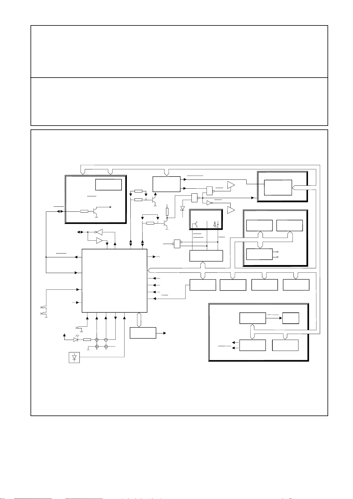
MULTI CONCEPT
MX-CHASSIS
Functional description
2
C
I
APSi filter/Strobe
Scart pin 10
Strobe
APSi
RGB status
FRONTEND
Multi: Strobe to write I/O-latch
Single: APSi control
(Single norm)
IF Ident.
Line-out
status
Rec / IR
IF ident.
resistor
47
55
3
6
HP ind
10
+5V
A/D
1
TV tuner
AV-link
µP
ICf3
61 62
Local control
T V
1997
4, 57, 8
Subwoofer
ident.
16:9 ident.
MSP Reset
PA-mute
263
46
64
50
PWM
M3L
SDA
SCL
A/D
TXT
ICr1
51
5
44, 45
54
A/D
53
52
A/D
7
4, 59, 60
49, 50, 51
Sound
processor
ICa2
24
12Vp
APSi
test
Hor. shift
Status 2
Status 1
Status 3
Hold
7
E3-control
9, 10
&
(3-state)
4
5
12V
28V
DSP Reset
Subwoofer
mute
&
Comb-Filter
module
13
Bypass /
Comb-ID
15
Deco/Sync
Service
3
connector
OR
mute
2
NTSC
16
ICd1
5, 6
1, 2
PIP-MODULE
Video switch
PIP/ext. RGB
mute
1
FSC /
SVHS
23
AUDIO FEATURE BOX
15
85
PA
Subwoofer
Mute
Int-LS
PA
FEATURE BOX DB7xx
Deflection
40,41
2
I
C
5, 6 2, 4 27, 28
NVM
ICf2
PIP tuner
16
Deco/Sync
15
ICp3
Surround
processor
2
IC 17
17, 18
40, 41
DPLL
IC 11
Video Switch
ICq1
L-norm
8
4, 5
5, 6
ICar2
37
38
Bridges:
1/2 FM
VGA
8
PIP µP
IQTV µP
IC 18
RGB processor
ICp1
17, 18
ICp6
IF
51, 61
8, 9
ICt1
9,10
3, 4
IR Receiver
Page 38

MICROPOWER-STEUERUNG
1
Allgemein
Das Netzteil ist mit einem Micropower-System ausgerüstet,
um denStromverbrauch in der Betriebsbereitschaft auf ca.
100 mW zu senken (dieserliegt im Normalfall bei ca. 5 bis 7
W). Um dieses zu ermöglichen, müssen das Netzteil und
die Entmagnetisierungsschaltung in der
Betriebsbereitschaft vollständig abgeschaltetsein. Das
einzige aktive Bauteil in der Betriebsbereitschaft ist die
Micropower-Schaltung, die ihre Versorgungsspannung von
einem kapazitivgekoppelten Gleichrichter bezieht. Dieser
liefert die Versorgungsspannung fürnötige Schaltkreise wie
einen „primären” Infrarotempfänger und ein Gatter. Wird
das Fernsehgerät mit demNetzschalter oder durch ein
Befehl der Fernbedienung eingeschaltet, steuertdas Gatter
einen Triac an, wodurch Netzspannung am Netzteil
vorhanden ist.Gleichzeitig steuert die MicropowerSchaltung den Hauptmicrocontroller über Optokoppler. Die
Micropower-Schaltung ist nicht netzisoliert.
Einschalten mit dem Netzschalter
Die Netzspannung wird direkt der Micropower-Schaltung
zugeführt, die sich aufder eingebauten Schalttafel befindet.
Die Schaltung bekommt ihreVersorgungsspannung von
dem kapazitiv gekoppelten Gleichrichter bestehend ausden
Kondensatoren Cfc24/26, den Widerständen Rfc23/24 und
den Dioden Dfc6...Dfc9. DieVersorgungsspannung wird
durch die Zenerdiode DZfc1 auf +5,1 V eingestellt undwird
zum Infrarotempfänger Hfc2, zum NAND-Gatter ICfc1 sowie
zur LED Dfc16weitergeführt, die den Anschluß an das Netz
anzeigt.
Das Fernsehgerät kann durch festes Drücken des
Netzschalters eingeschaltetwerden. Ein zusätzlicher Kontakt
im Netzschalter erzeugt einen LowLevel-Impuls über die
Diode dcf13 auf die Pins 12/13 des NAND-Gatters.Aufgrund
der Arbeitsweise des NAND-Gatters sind der Pin 11 wie
auch die Pins 5/6 auf LOW, wobei Pin 4 aufHIGH ist. Der
Transistor tfc1 leitet und erdet die Kathode im internen LED
desOptokopplers ICfc2. Der Optokoppler führt dann die
Netzspannung über denWiderstand Rfc27 zum Gatter des
Triac Dfc1. Der Triac erhält ausreichende Start
spannungüber Rfc27, nach dem Widerstand Rfc26 parallel
mit Rfc27 geschaltet wird, umden Triac im leitenden
Zustand zu halten. Hierdurch steht die Netzspannung fürdas
Netzteil zur Verfügung.
Ebenfalls gehen, wenn das Fernsehgerät mit dem
Netzschalter eingeschaltetwird, die Pins 1/2 des NANDGatters zeitweise auf LOW, der Pin 3 auf HIGH,während
der Transistor tfc6 leitet. Der Optokoppler ICfc4 leitet und
führt zurErdung der Kathode an der Diode dfc18. Dieses
zeigt dem Microcontroller an, daß dasFernsehgerät über
den Netzschalter eingeschaltet worden ist. Aufgrund
derEntladung des Kondensators Cfc31 gehen die Pins 1/2
auf LOW und sowohl derTransistor tfc6 als auch der
Optokoppler ICfc4 beenden den leitenden Zustand.
Das Netzteil erzeugt dann die Versorgungsspannung, der
Microcontroller wird zurückgesetzt und die Pins 47 (Pict_on)
und 48 (Rec_on) gehen auf LOW. Diesesveranlaßt den
Optokoppler ICfc3 die Haltepins 12/13 auf LOW zu setzen,
um dieTriac-Schaltung Dfc11 leitend zu halten.Wird der
Netzschalter nicht fest genug gedrückt, kann der zusätzliche
Kontaktnicht lang genug schließen und das Fernsehgerät
bleibt in der Betriebsbereitschaft.
3 des „primären” Infrarotempfängers die Kondensatoren
Cfc28und Cfc29. Folglich gehen die Pins 12/13 des NANDGatters auf LOW und derTriac leitet. Der Befehl muß
ausreichend lang sein, damit das Netzteilgenügend Zeit hat
um Versorgungsspannung zu erzeugen und der
Microcontroller zurückgesetztwerden kann, um den
Startbefehl vom „sekundären” Infrarotempfänger
zuerhalten. Anschließend gehen die Pins 47 (P_on) und 48
(Rec_on) desMicrocontrollers auf LOW und der
Optokoppler ICf3 leitet und hält die Pins 12/13 des NANDGatters auf LOW.
Wird das Fernsehgerät mit der Fernbedienung
ausgeschaltet, gehen die Pins 47(P_on) und 48 (Rec_on)
des Microcontrollers auf HIGH. Daher werden alle Vp-und
Vr-Spannungen ausgeschaltet (horizontale und vertikale
Stufen werdenausgeschaltet), der Optokoppler ICf2 leitet
nicht und bringt die Pins 12/13 des NAND-Gattersauf HIGH.
Der Optokoppler ICf2 leitet nicht und der Widerstand Rfc27
wird vomGate des Dfc11 getrennt.Der Widerstand Rfc26
allein ist nicht in der Lage, ausreichend Haltespannungzum
Triac zu liefern und somit wird das Netzteil vom Netz
getrennt.
Ein- und Ausschalten mit der Fernbedienung
Das Fernsehgerät muß selbstverständlich in
Betriebsbereitschaft sein. Der Kondensator Cfc29 wird über
rfc34 geladen, so daß der Level an den Pins 12/13des
NAND-Gatters HIGH ist. Wird der Befehl mit der
Fernbedienung gegeben,entladen die Impulse auf den Pin
Page 39

2
NETZTEIL
Allgemein
Das Netzteil ist ein SMPS. Die Netzisolierung wird durch
den Transformator Mo2durchgeführt. Die Netzspannung
wird durch die Dioden Do1 .... Do4doppelweg-
gleichgerichtet und vom Kondensator Co10 gefiltert. Diese
gefilterteSpannung wird zum Schalttransistor To1
(MOSFET) über die Primärwicklung 11 und 5
desNetztransformators geleitet. Während der Leitphase von
To1 wird Energie in derPrimärwicklung 11 und 5
gespeichert. Wird der Transistor To1 abgeschaltet,fließt die
Energie in die Sekundärwicklungen. Diese Impulse werden
durch die Sekundärdioden Do11... 14 und Do16
gleichgerichtet.
Die folgenden Versorgungsspannungen sind über die
Sekundärdioden verfügbar:
+130 V Horizontale Endstufe
+28 V Audioverstärker, Subwoofer und Audio-Feature-
Modul
+17 V +12 V IC-Regler, horizontaler Treiber und
Reglertransistor +8 Vp
+7 Vfb Feature-Box
+7 V +5 Vr IC-Regler, +5 Vstb IC-Regler und +7 V
Versorgungsspannung
Hinweis! Die Spannungswerte können - abhängig von der
Bildröhre-abweichen. Genauere Werte sind den
Stromlaufplänen zu entnehmen.
Das Netzteil ist für den Master-Slave-Betrieb konzipiert,
wobei derStromversorgungsregler ICo1als Sklave und der
sekundäre Regler ICo2 als Masterarbeitet. Das Netzteil
arbeitet in den verschiedenen Betriebsphasen
folgendermaßen:
Einschaltphase:
Das Netzteil befindet sich im primären Regelbetrieb (BurstBetrieb). Der Stromversorgungsregler ICo1 erzeugt
unabhängige Steuerimpulse für den Schalttransformator.
Betriebsphase:
Das Netzteil befindet sich im sekundären Regelbetrieb
(Master-Slave-Betrieb). Der sekundäre Regler ICo2 erzeugt
Steuerimpulse für den Stromversorgungsregler ICo1. The
secondary controller is synchronized to the line flyback
pulses.
Recording mode:
Power supply is in the secondary regulation mode (master-slave mode). Secondary controller ICo2 generates drive
pulses for power supply controller ICo1. The secondary
controller is synchronized to the free running frequency of
an internal oscillator.
Ausschalten in die Betriebsbereitschaft:
Das Netzteil befindet sich im primären Regelbetrieb (BurstBetrieb). DerStromversorgungsregler ICo1 erzeugt
unabhängige Steuerimpulse für den Schalttransformator.
Einschalten
Nach dem Einschalten mit dem Netzschalter - wenn die
Triac-Schaltung Dfc11 (auf der Microsteuerung) leitet - wird
der Kondensator Co15 über dieWiderstände Ro9, Ro11,
Ro70 und den Thyristor To19 aufgeladen. Wenn
dieStartspannung am Pin 16 des ICo1 den
Einschaltschwellenwert erreicht (dieser beträgt
normalerweise+11,8 V), geht der IC in Betrieb.
Die Versorgungsspannung des ICo1 wird dann von Pin 3
der Sekundärwicklung überdie Einweggleichrichter-Diode
abgenommen. Dieser Pin 3 der Wicklungübermittelt Impulse zur Diode Do9. Diese Spannung steuert den Transistor To9 zum Leiten und Erden des Schaltkreises vom
Thyristor To15.
Dieselbe Gleichspannung, die von der Kathode der Diode
Do9 abgenommen wird, dient zur Regelung des Netzteils.
Die Gleichspannung wird über den Netzfilter Ro26, Co28
und Ro24 zum Eingang desFehlerverstärkers an Pin 6
geleitet. Der Fehlerverstärker vergleicht die
Eingangsspannung mit der internen Referenz (+2,5 V) und
ändert die Burst-Zeit. Die Widerstände ro4 und ro10 stellen
die Spannung auf den richtigen Wert ein.
Eine eventuelle Magnetisierung des Transformators kann
durch Abfühlen derSpannung an den Pins 2 und 3 der
Wicklung festgestellt werden. DieseInformation wird über
den Widerstand Ro15 zum Pin1 des ICo1 weitergeleitet.
Wird der festgelegte Wert überschritten, können die
Ausgangsimpulse nicht erzeugt werden.
Um eine Magnetisierung während der Einschaltphase zu
vermeiden, wird derBetrieb mit der internen
Betriebsfrequenz des Oszillators - geteilt durch viergestartet, bis die Spannung am Softstart-Pin 9 einen Wert
von +2,5 Verreicht. Die Betriebsfrequenz des Oszillators
wird durch den Kondensator C016 an Pin 10 und
denWiderstand Ro3 an Pin 11 auf 27 kHz eingestellt.
Ansteuerung des Schalttransistors
Der Pin 14 gibt Rechteckimpulse zum Gate des
Schalttransistors To1. DieWiderstände R02 und Ro13
begrenzen den Gate-Strom. To1 leitet während
desPositivimpulses und der Absaugstrom fließt durch die
Pins 11 und 5 derPrimärwicklung. Die Klemmschaltung
Do6, Co11 und Ro16 begrenzt die Spannungsspitzen, wenn
To1ausgeschaltet wird. Die Quelle von To1 wird über
dieStrombegrenzungswiderstände Ro18, Ro19, Ro21 und
Ro22 geerdet. Die Informationüber diesen Strom wird zum
Pin 3 des Stromversorgungsreglers weitergeleitet.
Nach der Startphase, wenn die Versorgungsspannungen
erzeugt worden sind, gehtdas Netzteil vom primären in den
sekundären Regelbetrieb über. DerMicrocontroller wird
zurückgesetzt und die Pins 48 (P_on) und 49 (R_on)
gehenauf LOW. Die Leitung R_on ermöglicht es, über den
Transistor to6 und den Regler ICo3 +12 Vweiterzugeben.
Diese Spannung wird zum sekundären Regler ICo2 (Pin
2)weitergeführt und der IC geht in Betrieb.
Der Kondensator co58 an Pin 1 arbeitet als SoftstartKondensator, der die Dauer des Softstarts auf ca. 20ms
festlegt.
Betriebsbereitschaftsphase:
Durch die Micropower-Steuerung ist das Netzteil
vollständig spannungsfrei.
Das Netzteil verfügt ebenfalls über eine sogenannte Service-Betriebsbereitschaft. Das Fernsehgerät ist in der Service-Betriebsbereitschaft, wenn es durch Drücken der Tasten
-vol / menu, TV und i in den Servicemodus versetzt wird,
aber noch nicht durch zweimaliges Drücken der TV-Taste
eingeschaltet worden ist. Indieser Phase ist das Netzteil in
Betrieb (Burst-Betrieb), jedoch die Spannungen Vr und Vp
sind nicht vorhanden.
Die freischwingende Frequenz eines internen Oszillators
wird durch den Kondensator co72 an Pin 7 und den
Widerstand Ro37 an Pin 8 auf 32 kHz eingestellt. Im
Normalbetrieb wird der Oszillator durch die
Zeilenrückschlagimpulse über das Differenzierglied Ck6,
den Widerstand ro38 und die Diode Do18 synchronisiert.
Im Aufzeichnungsbetrieb werden die Spannungen Vp
ausgeschaltet und somit istdas Zeilenrückschlagsignal
nicht vorhanden. In diesem Fall ist der Oszillatorim
freischwingenden Betrieb.
Page 40

Der interne Schwingweitenmodulator wird durch Vergleich
der Eingangsspannungswerte an Pin 5 mit den
Sägezahnimpulsen des Oszillatorsverglichen. Der Pin 5 ist
über das Widerstandsnetzwerk Ro46, Ro44, Ro50, Ro45 und
Ro42 an +140 V angeschlossen. Mit dem
Trimmerpotentiometer Ro45 können die
Ausgangsspannungen des Netzteils geregelt werden.
Um ein übermäßiges Abfallen der Spannung auf +7
Vwährend des Aufzeichnungsbetriebs zu vermeiden, wird
die Diode Do20 von demoben erwähnten
Widerstandsnetzwerk mit +7 V versorgt. Falls der
Spannungswert weit unter +7 Vabfällt, leitet die Diode und
bewirkt einen niedrigeren Spannungswert an Pin5. Der
Regler erzeugt dann größere Impulse an Ausgangspin 3
und dieVersorgungsspannung des Netzteils wird erhöht.
Die weitenmodulierten Steuerimpulse werden von Pin 3
über den ImpulsüberträgerMo3 zum Pin 2 des Reglers für
das Netzteils übertragen. Die Anstiegflanke
derSteuerimpulse bewirkt das Leiten des Schalttransistors,
wobei dieAbfallflanke, die auf die Zeilenrückschlagimpulse
synchronisiert wird, den Transistorausschaltet.
Diese Anordnung verhindert Störungen, die durch die
Ausschaltzeit desTransistors beim Bildaufbau verursacht
werden.
Erkennung von Unter-/Überspannung
Der Stromversorgungsregeler besitzt einen internen Monitor für sowohl Unter-als auch Oberspannung an Pin 16.
Der untere Schwellenwert der Spannung ist normalerweise
+8,5 V. Niedrigere Spannungswerte sperren die
Ausgangsimpulse.
Der obere Schwellenwert der Spannung ist normalerweise
+15,7 V. Höhere Spannungswerte sperren die
Ausgangsimpulse.
Ein Neustart erfordert zuerst ein Sinken des
Spannungswertes an Pin 16 aufunter +8,5 V und
anschließend ein Steigen auf +11,8 V, bis der
Spannungswertüber den Kondensator Co22 +2,5 V erreicht
hat. In diesem Fall ist der Schaltkreisbetrieb vollständig
gesperrt.
3
Micropower-Systems sind in der Betriebsbereitschaft keine
Spannungen vorhanden.
Der ICo3 regelt die +12 Vr- und +12 VpVersorgungsspannungen. Die +12Vr-Spannung ist im Normal- und Aufzeichnungsbetrieb vorhanden, jedoch nicht
inder Service-Betriebsbereitschaft.
Die +12 Vp-Spannung kann im Aufzeichnungsbetrieb von
dem Microcontrollerausgeschaltet werden. In diesem Fall
ist die P_on-Zuleitung auf HIGH, derTransistor to7 leitet und
der Transistor to4 wird abgeschaltet.
Die +12 Vp- und +8 Vp-Spannungen sind nicht vorhanden
und deshalb ist diehorizontale Ablenkstufe nicht in Betrieb.
Der ICo6 regelt die +5 Vr-Spannung, die im Normal- und
Aufzeichnungsbetrieb, jedoch nicht in der ServiceBetriebsbereitschaft vorhanden ist.
Die Abstimmspannung von +30 V für den Tuner wird über
+130 V geregelt. DerSchaltkreis befindet sich in der
horizontalen Endstufe und besteht aus den Widerständen
Rk11 ... Rk114 und der Zenerdiode ZDk1.
Strombegrenzung
Wie oben erwähnt, ist die Quelle des Schalttransistors über
dasWiderstandsnetzwerk Ro18/19 und Ro21/22 geerdet.
Das Meßergebnis wird zumEingangspin 3 des Ico1
übermittelt. Es wird ein doppeltes Schwellensystem
verwendet; der erste Grenzwert von +0,6 V gegen
kurzzeitige Überlast und ein zweiter Grenwert von +0,8 V
gegen sehr hohe Überlast.
Ist der erste Schwellenwert erreicht, hört der
Schalttransistor bis zum Endeder Periode auf zu leiten. Soll
dieser wieder leiten, ist ein neuer Impulserforderlich.
Während der ersten Schwellenperiode wird der
Kondensator Co22 geladen. Falls der Spannungswert über
Co22 +2,5 V erreicht, wird der Ausgang gesperrt. Dieses
System wird „Repetitive Overload Protection” genannt.
Jedoch wird, wenndie Überlast absinkt bevor +2,5 V
erreicht worden sind, der Kondensator Co22entladen und
der Normalbetrieb fortgesetzt.
Falls eine sehr hohe Überlast den zweiten Schwellenwert
erreicht, wird derAusgang sofort gesperrt.
Wenn die Stromversorgung durch Überschreiten des ersten
Schwellenwertesunterbrochen worden ist, kann diese
durch Vermindern der Versorgungsspannungan Pin 16
unter +8,5 V und durch anschließendes Erhöhen auf +11,5
Vwiederhergestellt werden
Falls jedoch die Stromversorgung infolge von
Überschreiten des zweitenSchwellenwertes unterbrochen
worden ist, wird der Schaltkreis vollständigunterbrochen
und kann dann nur mit dem Netzschalter wieder in Betrieb
genommenwerden.
Regler / Spannungsschalter
Der ICo4 regelt den +5 Vstby-Spannung, die bei
arbeitendem Netzteil immervorhanden ist. Aufgrund des
Page 41
4
EMPFANG
Tuner / ZF
Der Tuner wird als „Front End”-Tuner bezeichnet, weil sich
der Tuner-Block undder IF-Block zusammen in einem Modul
befinden. Die Kanalabstimmung beruht aufeinem
Frequenzsynthesesystem in einem Frequenzbereich von
48.25 MHz bis 855.25MHz einschließlich der Kabel- und
Hyperbandkanäle.
In Multistandard-Fernsehgeräten werden beide Blöcke über
den IIC-Bus geregelt.Der IIC-Bus des ZF-Blocks arbeitet nur
im Einweg-Datenverkehr. In BG-Standard-Fernsehgeräten
hat der ZF-Block keine Schnittstelle zum IIC-Bus.
Multistandard-ZF-Block
Der Filter SAW501 arbeitet als Bildsignalfilter. Das Video
ZF-Signal wird zuden Pins 28 und 29 des Bild- /
Tondetektorschaltkreises IC501 geleitet.
Die Filter SAW502 (BG, DK, I, Nicam L) und SAW503 (Nicam
L’, L/L’ AM) arbeitenals Tonsignalfilter. Die Wahl des Standards erfolgt über die Dioden D501 undD502 und die
Transistoren T502 und T503. Die Transistoren werden über
den Pin7 des IIC-Bus-Expander (IC502) gesteuert. Die TonZF-Signale werden zu den Pins 31/32(BG, DK, I, Nicam L),
1/2 (Nicam L’) und 4/5 (AM L/L’) desDetektorschaltkreises
geleitet.
Die AGC-Einstellung wird über das Potentiometer P501 an
Pin 26 durchgeführt.Die Pins 20 und 21 sind Eingänge für
die Standardwahl, die vomIIC-Bus-Expander geregelt
werden. Die AFC-Information wird von Pin 11
zumTunerblock und weiter zum IIC-Bus gegeben. Die AGCRegelung wird über den Pin 27 zum
Tunerblockdurchgeführt. Die Tankspule des FPLL-VCO
befindet sich zwischen den Pins 14und 19. Diese PLLReferenzspule bestimmt den Haltepunkt eines
aufgefundenenKanals während der APSi. Die VCOFrequenz ist eine zweifache Videoträgerfrequenz (2 x 38,9
MHz =77,8 MHz). Bei vorliegendem L’-Standard wird die
VCO-Frequenz auf 67,8 MHz (2x 33.9 MHz) durch die
Standardwahl an den Pins 20 und 21 festgelegt und mitdem
Potentiometer P502 an Pin 20 eingestellt.
Das ZF-Tonsignal wird vom Pin 8 und das AM-Signal vom
Pin 7 zumMultistandard-Sound-Prozessor Ica2 geleitet.
Das CVBS-Signal wird vom Pin 23 zum GruppenlaufzeitKorrekturschaltkreis undzu den Verstärkern bestehend aus
den Transistoren T504 ... 514 und damitverbundenen
Bauteilen geführt. Das CVBS-Signal wird dann zur
Videomatrix ICq1geführt.
Standard Pin 11 Pin 13 Pin 14 Pin 7 Pin 6 Pin 5
B/G H L L L H H
I, K1 H L H H H H
D/K H H L H H H
LHHHLLL
L’ H H H H H L
Pin 11 steuert die Eingangsschalter des IC501. Der Pin
11 ist normalerweise auf HIGH. Während der
Kanalsuche (APSi) geht der Pin 11 auf LOW.Ein
niedriger Pegel an den Pins 27 und 28 des IC501
übermittelt dasVideo-ZF-Signal (anstelle der
Sound-ZF) zum FPLL-Block. Weil das Videoband
breiter ist, können Kanälesomit besser gefunden
werden.
Pin 13 steuert den Gruppenlaufzeit-Korrekturschaltkreis
Pin 14 wählt den Ausgang des Gruppenlaufzeit-
Korrekturschaltkreises
Pin 7 wählt den richtigen Sound-ZF-Filter
Pin 5/6 steuert die Eingangsschalter und den AM-
Demodulator und wählt dierichtige Modulation
und VCO-Frequenz
BG-Standard ZF-Block
Der BG-ZF-Block ist wesentlich einfacher aufgebaut als
derMultistandard-ZF-Block. Es ist nur ein SAW-Filter
vorhanden während derIIC-Bus-Expander, der
Gruppenlaufzeit-Korrekturschaltkreis sowie verschiedene
Schalttransistoren fehlen.
Während der Kanalsuche (APSi) steuert der Microcontroller
(Pin 47) denTransistor T501 zum Leiten an. Ein niedriger
Pegel an den Pins 27 und 28 gibtdas Video-ZF-Signal zum
FPLL-Block weiter, um das Auffinden von Kanälen
zuverbessern.
Abstimmung
Die Abstimmung wird mit dem APSi-System (Automatische
Programmsuche, Sortierenund Kanalidentifizierung)
durchgeführt. Zur Benennung und Identifizierung
derKanäle dient entweder PDC (Program Delivery Code),
VPS (Video ProgrammingSystem), NI (Nation Identification)
oder die Kopfzeile (Header) des Videotextes. DasSortieren
der Kanäle ist vom jeweiligen Land abhängig und wird
durch dieSoftware bestimmt.
Der Schaltkreis IC502 arbeitet als IIC-Bus-Expander (8-Bit
Shift Register).Die Transistoren T515 und T516 trennen den
IIC-Bus von den Pins 2 und 3, ummögliche Fehlfunktionen
am IIC-Bus auszuschließen, wenn das
Fernsehgerätausgeschaltet wird.Die Bestimmung des
Standards findet über den IIC-Bus statt. DerMicrocontroller
sendet Daten zum Schieberegister, die Ausgänge ändern
gemäßder Daten ihren Zustand und der Ausblendimpuls
schaltet auf die Ausgänge. DerAusblendimpuls (hoher
Pegel) wird vom Microcontroller (Pin 47) zur Basis des Transistors T517 undweiter zu Pin1 geführt. Zusätzlich arbeitet
der Basiswiderstand (R556) vonT517 als Anzeige der
eingebauten ZF-Modulversion. Der Nennwert
diesesWiderstandes hängt von der Modulversion ab. Der
Pin 55 des Microcontrollers liest die Spannungzwischen
diesem Widerstand und dem Übergang zum Basisemitter
ab und erkennt sodie Modulversion.
Die Daten vom Microcontroller bestimmen die Ausgänge
des IC502 bezüglich desÜbertragungsstandards wie folgt:
Page 42
6
Die Pinfunktionen des SoundProzessors:
Pin I / O Kurzbeschreibung
04 O DSP zurücksetzen und ausschalten
bei LOW
05 O Subwoofer ausschalten bei HIGH
07 I Versorgungsspannung +5 Vr
09 I I2C Takt (SCL)
10 I/O I2C-Daten (SDA)
11 O I2S Takt
12 I/O I2S Wortwahl
13 O I2S-Datenausgang
14 I I2S1 Dateneingang
18 Digitale Stromversorgung +5Vr
19 Digitale Erdung
20 I I2S2-Dateneingang
24 I MSP einschalten / RESET bei LOW
25 O Kopfhörerausgang, R
26 O Kopfhörerausgang, L
28 O Lautsprecherausgang, R
29 O Lautsprecherausgang, L
31 O subwooferausgang
33 O Scart-Ausgang, R
34 O Scart-Ausgang, L
36 O Scart-Ausgang, R
37 O Scart-Ausgang, L
38 Pegelkondensator (Hp amp)
39 Analoge Stromversorgung +8.0V
40 Pegelkondensator (Ls amp)
42 Analog ref V, Hochspannungsteil
43 I Scart-Eingang, L
44 I Scart-Eingang, R
46 I Kamera-Eingang, L
47 I Kameraeingang, R
49 I Scart-Eingang, L
50 I Scart-Eingang, R
52 I Scart-Eingang, L
53 I Scart-Eingang, R
54 Referenzspannung ZF A/D Wandler
55 I Monoeingang
57 Analoge Stromversorgung +5Vr
58 I ZF-Eingang 1
59 I ZF-Eingang (allgemein)
60 I ZF-Eingang 2 (Tuner SIF)
62 I Schwingquarz 18.432 MHz
63 O Schwingquarz
Verstärker für Kopfhörer, Ica3
Audiosignale vom Sound-Prozessor werden zu den
invertierenden Eingangspins 2(L) und 6 (R) geleitet. Die
Ausgänge zum Kopfhöreranschluß sind von den Pins 1(L)
und 7 (R). Im Kopfhöreranschluß ist ein Schalter, der dem
Microcontrollerübermittelt, wenn ein Kopfhörer
angeschlossen ist. Die Lautstärkeregelung für
denKopfhörer erscheint dann zusätzlich zur
Lautstärkeregelung für den Lautsprecher im Display.
Audioleistungsverstärker, ICa1Das
Audiosignal wird durch den Zweikanal-HiFiAudioleistungsverstärker TDA2616verstärkt. Der Verstäker
hat ein eingebautes Schutzsystem gegen Kurzschluß
undthermische Überlast. Er ist auch mit einem internen
Stummschaltungseingangausgestattet, der unerwünschte
Signale an den Eingängen beim Ein- oder Ausschalten
desFernsehgerätes abschwächt.
Die Audiosignale werden vom Audioprozessor zu den Pins
1 (L) und 9 (R)geleitet. Ein LOW an Pin 2 schaltet den
Verstärker stumm. DasStummschaltesignal wird vom
Microcontroller (Pin 51) über die Transistoren ta10, ta4 und
ta3 abgenommen. Ein hoher Pegel an Pin 51 des
Microcontrollers bewirkt eine sogenannte „zentrale
Stummschaltung”, was eine Stummschaltung aller
Audioleistungsverstärker ist.
Die Versorgungsspannung +28 V wird vom Netzteil zu Pin
7 geführt. Dieverstärkten Audiosignale für die Lautsprecher
kommen von den Pins 4 (C) und 6 (R). DerScheinwiderstand
des internen Lautsprechers beträgt 8 ohm und der
minimaleScheinwiderstand des externen Lautsprechers
beträgt ebenfalls 8 ohm. Ist einexterner Lautsprecher
vorhanden, wird der interne Lautsprecher durch einen
Schalter imLautsprecheranschluß stummgeschaltet.
Page 43
VIDEOBAUGRUPPE
7
Die Videobaugruppe ist in folgende Funktionseinheiten
aufgeteilt:
- Videokoppelung / Scartanschlüsse
- Farbdecoder / Synchronisierprozessor
- Basisband-Verzögerungsleitung
- Feature-Boxen- RGB-Videoprozessor- CRT-Modul
- Videotext
Videokoppelun
Der TEA6417 ist ein über den IIC-Bus gesteuerter
Signalschalter, der ein Schalten von 8 Eingangsquellen auf
6 Ausgänge ermöglicht. Jeder Ausgang kannnur an einem
Eingang angeschlossen werden, jedoch kann ein Eingang
anverschiedene Ausgänge angeschlossen werden. Die
Bandbreite beträgt 15 MHz und dieNominalverstärkung von
Eingang zu Ausgang ist 6,5 dB. Alle
Schaltmöglichkeitenwerden über den IIC-Bus mit den Pins
2 (SDA) und 4 (SCL) gesteuert. DerSchaltkreis arbeitet mit
einer Versorgungsspannung von +10 V, die zu den Pins 9
und 12 geleitet wird. Diese+10 V werden von der
Zenerdiode Zdq1 mit +12 Vr geregelt.
Die Ein- und Ausgänge sind wie folgt verbunden:
Eingang Signal Quelle
1 CVBS Scart 3
3 CVBS Scart 1
5 C Scart 2
6 CVBS / Y Scart 2
8 CVBS / Y Cam-Anschluß
10 C Cam-Anschluß
11 CVBS Tuner
20 CVBS Bild-in-Bild-Tuner
Ausgang Signal Ziel
13 CVBS / Y Decoder / Kammfilter
14 C Decoder / Kammfilter
15 CVBS / Y Bild-in-Bild-Modul
16 C Bild-in-Bild-Modul
17 CVBS / Y Scart 2
18 CVBS Videotext
Scart 1
Der Scart 1 ist vollständig angeschlossen, d.h., daß dessen
RGB-Eingangebenfalls verfügbar ist. Im RGB-Modus wird
das Schnellaustastsignal vonScartpin 16 zu Pin 18 des
Farbdecoders und über tq3, tq4, Cq32 (und NAND-Gatter
icf4-4) zu Pin 6 des Microcontrollers geleitet.Das RGBBetriebssignal wird zum Microcontroller übermittelt, um
die richtigeEinstellung der H-Lage zu aktivieren. Es
ermöglicht ebenfalls dem Farbdecoder,den Eingang
zwischen RGB-Signal und verarbeiteten YUV-Signalen zu
wählen. Die Wahl wird durch einen Schaltblock im
Farbdecoder über den IIC-Bus bewerkstelligt.
Der Scart 1 hat einen festen Ausgangsanschluß für den
Tuner CVBS von Scartpin19 über die Transistoren tq9 und
Tq2.
Der Scart 1 arbeitet auch als AV-Verbindungsanschluß. Der
Ausgang derAV-Verbindung geht von Pin 2 des
Microcontrollers weiter über den Transistortq7 und den
Scartpin 10. Der Eingang der AV-Verbindung geht vom
selbenScartpin weiter über die Diode dq4 und Transistor
tq8 zu Pin 63 des Microcontrollers. Das System derAVVerbindung ermöglicht einen Datentransfer zwischen dem
Fernsehgerät undbeispielsweise einem Videorecorder.
Das System basiert auf dem „P50"-Standard und
ermöglicht z.B. den Transfer vonKanalabstimmdaten und
EPG-Programmierung (Electrical Program Guide).
Scart 2
Zusätzlich zum S-VHS-Eingang ist der Scart 2 als Ausgang
für S-VHS-Signalevorgesehen, die von den Kamera
anschlüssen kommen. Der Ausgang desLuminanzsignals
führt über den Transistor Tq1 und das des Farbwertes über
tt3und tt2. Der Scart 2 dient auch als AV-Verbindung.
Scart 3 (Option)
Der Scart 3 ist ein optionaler Anschluß mit den gleichen
Eigenschaften wieScart 1.
Genauere Informationen sind in Abschnitt „Optionen,
TA710" enthalten.
Farbdecoder / Synchronprozessor,
ICd1
Allgemein
Der TDA9413 ist ein IIC-Bus gesteuerter, selbsteinstellender
PAL / NTSC /SECAM-Decoder / Synchronprozessor.
Der Farbdecoder kann sowohl CVBS- als auchY/C-Signale
verarbeiten. Die integrierte Schnellschaltung wählt
entweder dasY-Signal mit den UV-Eingangssignalen oder
YUV-Signale bestehend aus RGB-Eingangssignalen.
Der Synchronprozessor erzeugt einen zweistufigen
Sandcastle-Impuls (SC), einenhorizontalen
Synchronimpuls (HA) sowie einen vertikalen
Synchronimpuls (VA).
Eingangsschalter
Der Schaltkreis verfügt über einen Zweipin-Eingang für die
CVBS- (Pin 26) oderdie Y/C-Eingangssignale (Pins 26 und
25). Die Wahl zwischen den Signalen gehtüber den IC-Bus.
RGB-Farbmatrix
Die RGB-Signale von Scartanschluß 1 (oder von
Scartanschluß 3) werden zu denEingangspins 19 (B), 20
(G) und 21 (R) übermittelt. Die RGB-Farbmatrix
wandeltRGB-Signale in YUV-Signale um. Das erforderliche
Eingangssignal wird durch denSchnellschalter zwischen
den umgewandelten und entschlüsselten YUV-Signalen
gewählt.Dieser Schalter wird durch das
Schnellaustastsignal an Pin 18 gesteuert.
Luminanzverarbeitung
Von Eingangspin 26 wird das CVBS/Y-Signal über den YKlemmkreis zu denGyrator-Kondensator-Sperrfiltern
geführt, einschließlich der einstellbaren
Luminanzverzögerung und des Farbwert-Sperrfilters. Die
Luminanzverzögerunggleicht die Verzögerung aus, die
durch die externe Basisband-Verzögerungsleitung für
dieUV-Signale verursacht wird. Der Farbwert-Sperrfilter
kann auf 4.43 MHz (PAL /NTSC), 4.28 MHz (SECAM) oder
3.58 MHz (NTSC) eingestellt werden. Die Schaltungwird
über den Schaltkreis für die Standarderkennung gesteuert.
PAL Y-, NTSC 3.58 Y- (vomKammfilter) und S-VHS Y-Signale
umgehen die Farbwertsperrfilter, um dieSignalbandbreite
einzuhalten. Die Umgehungsfunktion geschieht
automatisch überden IIC-Bus im S-VHS-Modus und bei PAL
/ NTSC 3.58-Empfang, wenn der Kammfilter installiertist.
Nach der Farbwertsperre wird das Y-Signal zur Schaltstufe
und von Pin 12zum Feature-Box-Modul geleitet.
Page 44

8
Chrominanzverarbeitung
Vom Eingangsschalter wird das CVBS / C-Signal durch den
ACC-Verstärker zu denFarb-Bandpaßfiltern geleitet. PAL C,
NTSC 3.58 C- (vom Kammfilter) und S-VHSC-Signale
umgehen diese Bandpaßfilter um die Signalbandbreite
einzuhalten. Der Farbwert wird dann zur
Standarderkennung und den Farbdecoderstufen
weitergeleitet.
Der Schaltkreis der Standarderkennung ist ein digitaler
Schaltkreis ohneexterne Bauteile. Die Quarze an Pin 30
(Bezugsquarz) und 31 (zweiter Quarz)legen die Standards
fest, die entschlüsselt werden können. Der IIC-Bus dient
zur Anzeige derangeschlossenen Quarze, um eine saubere
Einstellung der Kalibrierschaltkreisezu ermöglichen. Die
Bauteile an Pin 29 bilden den PLL-Farbfilter. Der Pin
23steuert den Multiplexer-Schaltkreis am
Kammfiltermodul, um die S-VHS-Signale im Multiplexer
(„L”) zu umgehen oder um Signale weiter zum KammfilterIC („H”) zuübermitteln. Zusätzlich dazu führt der Pin 23 die
Hilfsträgerfrequenz (Fsc)vom aktiven Quarz zum
Kammfilter-IC. Nach dem PAL / NTSC-Demodulator und
dem SECAM-Demodulator werden die Signalezur
Schaltstufe geleitet, die über den Schaltkreis der
Standarderkennunggesteuert wird. Schließlich gehen die
Farbdifferenzsignale von den Pins 2 (U) und 1 (V) zur
Basisband-Verzögerungsleitung.
Von der Verzögerungsleitung werden die
Farbdifferenzsignale an die Pins 3 (U)und 4 (V) geleitet,
dann weiter zur Schaltstufe und von den Pins 14 (U) und
13(V) zum Feature-Box-Modul geleitet.
Synchronverarbeitung
Das CVBS / Y-Signal wird durch den Synchronseparator
zum Horizontal-PLL undzum vertikalen Synchronseparator
geleitet.
Hauptbestandteil desSynchronschaltkreises ist ein 432 x
fH (6.75 MHz) Oszillator. Diese Frequenzwird durch 432
geteilt um den Phasendiskriminator für das eingehende
Signal zu festzulegen. DieZeitkonstante für die Schleife
kann gewählt werden, um entweder im schnellenModus,
im Auto-Modus oder langsamen Modus unter Verwendung
des IC-Bus zu sein.Die freischwingende Frequenz des 432
x fh-Oszillators wird von einem digitalen
Schaltkreisbestimmt, der auf den aktiven Quarz festgelegt
wird. Die Bauteile an Pin 24bilden den horizontalen PLL.
Die Phasenschleife kann mit dem IIC-Bus aufgelöstwerden.
Dieses vereinfacht die Bildschirmhinweise. Wenn kein oder
nur ein sehrrauschiges Signal vorhanden ist, kann die
Phasenschleife gelöst werden, umeine stabile
Zeilenfrequenz und somit eine stabile
Bildschirmdarstellung zuerzielen.
Der horizontale Synchronimpuls (HA) wird vom Taktgeber
über den Ausgangspin 17 zur Feature-Box übermittelt.
Das vertikale Teilersystem besitzt einen voll integrierten
vertikalen Synchronseparator. Der Teiler funktioniert
sowohl bei Systemen mit 50 Hz alsauch bei welchen mit
60 Hz. Er kann entweder die Teilbildfrequenz automatisch
bestimmen oder er kann auf die gewünschte Frequenz mit
dem IIC-Bus eingestellt werden.
Das Teilersystem besteht aus einem Zeilenzähler, einem
Normzähler, einem Taktgeber und einem Regler. Das System arbeitet mit dem 432-fachen der horizontalen
Zeilenfrequenz. Der Zeilenzähler empfängt
Freigabeimpulse mit der doppelten Zeilenfrquenz, so daß
er zwei Impulse pro Zeile zählt. Dieses Zählergebnis wird
demRegler übermittelt. Der Regler kann kann in einem von
drei Zählzuständen sein:Norm, normnah oder keine Norm.
Wenn der Zähler im Normzustand ist, erzeugt
erautomatisch einen vertikalen Synchronimpuls (VA) durch
den Taktgeber. Der VA-Impulswird über den Ausgangspin
11 zur Feature-Box geleitet.
Noise detector
The decoder includes an internal S/N ratio detector, which
was originally designed to control the PALplus signal proc-
ess. During PALplus transmission, the detector measures
the S/N ratio of the input signal on pin 26. When the S/N
ratio is over 20dB, the signal is accepted and the helper
signal is processed in the PALplus decoder. If the S/N ratio
is below 20dB, the PALplus process is disabled, and the
signal is handled as a normal signal. The detector can be
activated / deactivated via the IIC-bus.
In the Multi Concept, this detector is used to drive the APSi
system to accept or bypass tuned channels. The detector
controls the APSi system via the IIC-bus and it works only
during the automatic channel search.
However, the limit value of the bypass criteria (fixed 20dB)
seems to be too high for this purpose and therefore the
APSi may be too sensitive and bypass channels that it could
accept.
On the other hand, if the tuning system does not include
any signal level qualification, the APSi system accepts all
multiple and very noisy channels.
Utilizing an existing detector and avoiding both above
mentioned disadvantages, an external LPF filter is implemented. This filter is located at the luminance / CVBS input
(pin 26) and it consists of switching transistors tq10 / tq11,
and RC filter rq85 / cq45.
The RC-coupling is designed to filter high frequencies
(noise) from the luminance / CVBS signal.
When the S/N ratio of the tuned signal on pin 26 is over
20dB, the filter is not activated, but the channel is accepted
as such and it will be memorized and named.
If the S/N ratio is below 20dB, the detector causes a high
level on output pin 16. Transistor tq11 conducts and the
RC-coupling filters noise from the signal improving the S/
N ratio at the decoder input. When this noise-filtered signal is fed to the detector, it considers the S/N ratio to be
better than it actually is and accepts it. This channel will be
memorized, but not named.
In any case if the S/N ratio of the noise-filtered signal stays
below 10dB, it will be completely bypassed.
By tricking the detector in this way, the signal level qualification is reduced from an S/N ratio of 20dB to 10dB.
Sandcastle-Impuls
Der Synchronteil erzeugt auch einen zweistufigen
Sandcastle-Impuls (SC) am Pin10. Dieser Impuls wird nur
für Taktaufgaben in derBasisband-Verzögerungsleitung
verwendet.
IIC-Bus
Der Decoder / Synchronprozessor ist über die Pins 5 (SCL)
und 6 (SDA) mit demIC-Bus verbunden. Die Busaddresse
wird durch Anschluß von +8 V an Pin 22bestimmt.
Der Ausgangspin 16 steuert die Filterart des Kammfilters,
entweder PAL 4.43MHz (“L”) oder NTSC 3.58 MHz (“H”).Der
Eingangs- / Ausgangspin 15 wird hauptsächlich zur
Überprüfung verwendet,ob das Kammfiltermodul installiert
bzw. nicht installiert wurde. Diesesgeschieht durch
Überprüfung des Transistors tc3 (Basis-KollektorÜbergang).Zusätzlich steuert der Pin 15 den Kammfilter-IC
für den Filterbetrieb („H”) oder für deninternen
Umgehungsbetrieb („L”) an.
Basisband-Verzögerungsleitung
Allgemein
Der Schaltkreis TDA4665 ist eine Verzögerungsleitung, die
keine Einstellungenerfordert. Sie beinhaltet zwei
Kammfilter für die Farbdifferenz und arbeitetmit der Technik
von geschalteten Kondensatoren.
Jeder Kammfilter besteht aus einem unverzögerten
Signalpfad und einem mit 64µs verzögerten Signalpfad.
Im PAL-Modus arbeiten die Kammfilter als geometrischer
Addierer, um dieerforderliche PAL-Demodulation
auszuführen.Im NTSC-Modus unterdrücken die Kammfilter
Farbüberschneidungsstörungen.
Im SECAM-Modus wiederholt der Schaltkreis das
Farbdifferenzsignal aufaufeinanderfolgenden horizontalen
Abtastzeilen.
Page 45

Funktionsbeschreibung
Die Farbdifferenzsignale werden zu den Inputpins 14 (U)
und 16 (V) geleitet.Erst werden die Signale geklemmt und
nachfolgend durch Vorverstärker zu denverzögerten bzw.
unverzögerten Signalpfaden geführt. Alle im
Verzögerungsprozess nötigen Schaltsignale werden von
der 3 MHz-Haupttaktfrequenz erzeugt. Diese Frequenzwird
vom internen 6 MHz-VCO geteilt, der durch den SandcastleImpuls (SC)zeilengekoppelt wird. Der von dem
Synchronprozessor kommende SC-Impuls wird zu Pin 5
geleitet.
Verzögerte Farbdifferenzsignale werden durch die
Additionsschaltkreise zu denAusgangspuffern geführt und
schließlich an den Pins 12 (U) und 11 (V)ausgegeben.
Feature-Boxen, DB7**
Die Feature-Box hat zwei Hauptfunktionen; einmal die
Umwandlung des 50 (60)Hz-Rasters in ein Rasterformat von
100 (120) Hz und eine Verbesseung der Bildqualität.
Feature DB711 DB710
100 Hz Flimmerreduzierung - Bildwiederholung - Mittelwertinterpolation
Reduzierung des Zwischenzeilenflimmerns - nein - Mittelwertfilter
Rauschreduzierung - nein - bewegungsangepaßt
Umwandlung der Seitenverhältnisse
- horizontal - ±12.5 und ±25 % - ±12.5 und ±25 %
- vertikal - durch Ablenkung - +12.5 und +25 % (durch DSP)
- horizontale Bildposition - voll programmierbar - voll programmierbar
- anheben - nein - ja
- Seitenflächen - grau programmierbar - grau programmierbar
Bildschärfe - vertikale / horizontale Spitzen - vertikale / horizontale Spitzen
- CTI, LTI - CTI, LTI
Histogramm-Ausgleich - ja - ja
Standbild - ja - ja
A/D-Umwandlung - YUV 4:1:1 Signalformat - YUV 4:1:1 Signalformat
- 8-Bit pro Komponente - 8-Bit pro Komponente
- Eingangssignalamplitude angepaßt - Eingangssignalamplitude angepaßt
- Abtastfrequenz - 13.5 Mhz - 13.5 MHz
D/A-Umwandlung - Y-Komponente 9-Bit - Y-Komponente 9-Bit
- U- und V-Komponente 8-Bit - U- und V-Komponente 8-Bit
- Abtastfrequenz - 20.25 MHz ... 36 Mhz - 20.25 MHz ... 36 MHz
Feldspeicher - 3 Mbit (1 x 3 Mbit) - 6 Mbit (2 x 3 Mbit)
Synchronisierung - zeilengekoppelter Betrieb - zeilengekoppelter Betrieb
- Synchronisierung auf Quarzbasis - Synchronisierung auf Quarzbasis
Abhängig von der Chassisversion gibt es unterschiedliche
Feature-Boxen mit mehr oder weniger verschiedenen Features. Die komplette Signalverarbeitung istdigital und alle
Funktionen werden über den IIC-Bus gesteuert.
Die Basisversion ist die DB711, die nur einen 3 Mb großen
Feldspeicherenthält. Die Verwendung nur eines
Feldspeichers ermöglicht die Umwandlungeines 50 (60) HzVideos in ein 100 (120) Hz-Video, jedoch keine
Reduzierungvon Zwischenzeilenflimmern oder Rauschen
sowie vertikale Zooms.Dieses Modul ist für Fernsehgeräte
mit einem Seitenverhältnis von 4:3 konzipiert.
Die Version DB710 enthält zwei 3 Mb große Feldspeicher,
so daßRauschreduzierung und vertikale Zooms auch
enthalten sind. Die Version DB710(und DB700) sind für
Fernsehgeräte mit beiden - 4:3 und 16:9 -Seiten
verhältnissen.
Die Version DB700 ist eine „Full Feature”-Version, die
zusätzlich zu denFeatures der DB710 eine
Signalschnittstelle entsprechend dem VGAStandardenthält.
9
Feature-Box DB711
Die Hauptbauteile der DB711 sind ein A/D-Wandler, ein
Feldspeicher (FM), einSchaltkreis zur Verbesserung der
Bildqualität, ein digitaler Phasenregelkreis(DPLL) und ein
Ablenkungsregler.
Y-, U- und V-Eingänge
Die Luminanz- (Y) und Farbdifferenzsignale (U und V)
werden vom Farbdecoderzum Modulanschluß Q101 an die
Pins 6 (Y), 7 (U) und 8 (V) geleitet. JedesSignal wird zuerst
verstärkt und anschließend durch die Tiefpaßfiltergefiltert.
Danach werden die Signale über die Puffertransistoren zum
A/D-Wandler an die Pins 63(Y), 50 (U) und 31 (V) geleitet.
Analog-Digital-Wandler, ic9
Die Analog-Digital-Umwandlung wird mit Hilfe des A/DWandler-SchaltkreisesTLC5733 ausgeführt, der drei
getrennte 8-Bit A/D-Wandler enthält. Jedes Signalwird
durch den horizontalen Synchronimpuls an Pin 5 geklemmt
und dann indigitale Form umgewandelt. Die Wandler tasten
die Signale bei einer Abtastfrequenz von 13,5MHz ab. Die
Abtastfrequenz wird an Pin 56 übermittelt. Die Wandler
werdendurch die Referenzspannungen REFH (Pins 61, 52
und 29) sowie REFL (Pins 1, 48und 33) gesteuert.
Wird ein Überlauf ermittelt, werden die
Referenzspannungen entweder erhöhtoder verringert.
Hinweise über einen möglichen Überlauf werden an
denAusgangspins für die Luminanz (Pins 6...13) abgelesen
und zum NAND-Gatter ic28und weiter zum DPLLSchaltkreis ic11 an Pin 42 (ADC_OVFL) geführt. Dieser
Schaltkreis ermitteltdie Überlaufwerte und verändert, falls
erforderlich, die Impulsweite an Pin 43(PWM_REF). Diese
in der Weite geänderten Impulse werden zum
Tiefpaßfilter(bestehend aus den Transistoren t1 und t9 und
dem damit verbundenen Kondensatornetz)geleitet. Der
Tiefpaßfilter erzeugt beide Spannungen, REFH und REFL;
diesewerden zur Steuerung der A/D-Wandler zugeführt.
Nach Durchlaufen der Wandler werden die Signale zum
Ausgangsformat-Multiplexergeleitet, der von den Pins 45
(Modus 1) und 46 (Modus 2) gesteuert wird. Die
Kombination eines Tiefpegelzustands an beiden Pins
erzeugt ein Datenformatder YUV-Signale von 4:1:1. Die Uund V-Komponenten weisen 1/4 derSignalstärke der YKomponente auf.
Der Datenbus für Luminanz (Pins 6...13) istacht Bits breit
und der Datenbus für die Chrominanz (Pins 17...20) ist vier
Bits breit.
Page 46
10
Feldspeicher, ic14
Der Feldspeicher 1 (FM1) ist ein 3 Mb großer, High-SpeedDRAM. Der Schaltkreiswird als Speicherschaltkreis in der
Aufwärtsumwandlung 50 Hz auf 100 Hz undbei bestimmten
horizontalen Zoomfunktionen benutzt.
Die Luminanz- und Chrominanzwerte werden vom A/DWandler an die Pins 2...13 übermittelt. Der Schreibvorgang
wird unter Verwendung der Eingangssteuersignale RSTW
(RESETWRITE) an Pin 15, SWCK („Serial Write Clock”) an
Pin 14 sowie ENW („EnableWrite”) an Pin 16 durchgeführt.
Die Schreibtaktfrequenz (SWCK/CLK27_1) beträgt27 MHz.
Das ENW-Signal ermöglicht ein Beschreiben des Speichers
nur bei jedem zweitenTaktzyklus.
Der Lesevorgang wird unter Verwendung der LeseAusgangssteuersignale RSTR (RESET READ) an Pin 22,
SRCK („Serial Read Clock”) an Pin 23 sowie ENR(„Enable
Read”) an Pin 21 durchgeführt. Die Lesetaktfrequenz ändert
sichabhängig vom Bildformat Das IQTV kann folgende
Formate erzeugen (abhängig von Feature-Box
undSoftware):
36.000 MHz = - 25.0 % horizontale Kompression
30.375 MHz = - 12.5 % horizontale Kompression
27.000 MHz = 0 keine Kompression / keine
Expansion
23.625 MHz = + 12.5 % horizontale Expansion
20.250 MHz = + 25.0 % horizontale Expansion
Die vertikale Kompression wird durch den
Abenkungsprozessor ausgeführt. Nurdie DB710 und DB 700
beinhalten die vertikale Expansion (FM2 erforderlich).
Die Luminanz- und Chrominanzwerte werden über die Pins
24...35 an das IQTV2geleitet.
IQTV2-Schaltkreis, ic18
Die Hauptfunktion des IQTV2-Schaltkreises (Verbesserte
Fernsehqualität) istdie Aufwärtsumwandlung, die durch
das Zeilensprungverfahren verursachte Flimmern reduziert.
Der Grundgedanke dieser Aufwärtsumwandlung ist die
Umwandlung des 50 (60) Hz-Zeilensprungrasters in ein 100
(120) Hz-Rasterformat.
Die Flimmerreduzierung (Aufwärtsumwandlung) im DB711Modul basiert auf einerBildwiederholungsrate für die
Lumianz- und Chrominanzsignale. Das
Bildwiederholungsverfahren arbeitet mit einer Null-GradInterpolation undstellt das ursprüngliche Bild zweimal dar.
Die Eigenschaften des IQTV2 ermöglichen den Gebrauch
der horizontalen undvertikalen Zoomfunktionen; da aber
nur ein Feldspeicher vorhanden ist, kannnur die horizontale
Zoomfunktion benutzt werden. Daher werden alle
vertikalenZoomfunktionen über die Ablenkungssteuerung
durchgeführt
Die Einstellung der Bildschärfe ist nicht nur in horizontaler,
sondern auch invertikaler Richtung durchführbar. Die
Spitzenstufe besteht aus Hochpaß- und Bandpaßfiltern, die
den mittlerenBandfrequenzbereich verstärken, in dem sich
die meisten Details und Kantenbefinden.
Die Farbübergangsverbesserung (CTI) stellt die Flanken der
Farbkanten durchSteuerung der Eingänge zwischen
verzögerten, kommenden und laufenden
Chrominanzsignalen steiler. Ein neues Feature im CTI des
IQTV2 gewährleistet,daß die Mitte des Farbübergangs im
Vergleich von Eingangs- und Ausgangssignal immer an
dergleiche Stelle ist.
Die Luminanzübergangsverbesserung (LTI) wird durch
Abnahme einesDreipunkt-Mittelwertes dreier
Zwischensignale, Spitze, Maximum und Minimum
durchgeführt. Steilere Luminanzübergänge ohne Unterbzw. Übersteuern sind einErgebnis des LTI-Prozesses.
Das Histogrammausgleichssystem (HEQ) ist für eine
automatischeKontrastverstärkung konzipiert. Dieses System ermöglicht die Ausgabe einesgleichmäßigen
Histogramms für das Ausgangsbildsignal durch Austausch
derursprünglichen Pixelwerte durch neue unter
Verwendung einer nicht-linearen Umsetzung. Als Ergebnis
werdensowohl unter- als auch überkontrastierte Bildsignale
ausgeglichen, um dengewünschten Kontrast und die
Graustufenverteilung zu erhalten.
Pinbeschreibung:
Pin Symbol Beschreibung
1, 5-12, 14-15, D0_FM1...
18-21, 100 D15_FM1 Dateneingabe von FM1
2, 16, 41, +3.3V Stromversorgung
56, 81 (Spulenkern) für Logikschaltung
3, 28, 61, 77 +5V (i/o, AC) Stromversorgung für I/O
4, 29, 60, 69 GND (i/o, AC) Masse für I/O
13, 34, 78 +5V (i/o, DC) Stromversorgung für I/O
17, 37, 57,
79, 99 GND (CORE) Masse für CORE
22 FM1_ENR Lesen möglich, FM1
23 FM1_ENW Schreiben möglich, FM1
24 FM1_RSTW RESET Schreiben, FM1
25 HS_IPLL Horizontal-
synchronisation
26 FM2_ENW Schreiben möglich, FM2
27 FM2_ENR Lesen möglich, FM2
30 CLK_IPLL) Systemeingangstakt
(CLK27_1) (27 MHz)
31 CLK_OPLL
(CLK) Systemausgangstakt
32 VS_50 Vertikalsynchronisation
33 HS_OPLL Ausgang Horizontal-
synchronisation
35 HS32 32 kHz Horizontal-
synchronisation
36 FM_RSTR RESET, FM2W/R, FM1R
38 SDA IIC-Bus, serielle Daten
39 SCL IIC-Bus, serieller Takt
40 FSY Formatsynchronisation
für ADC
42 +5V (analog) Analoge Spannungs-
versorgung für DAC
43 VBIAS Analog
44, 47, 49, 51 GND (Analog) Masse für DAC
45 VT Analog
46 Vref Stromreferenz für DAC
48 AY Analoger Y-Ausgang
50 AV Analoger V-Ausgang
52 AU Analoger U-Ausgang
53 RST RESET System
54 TEST_EN Testbetrieb möglich
55 VS_50_100 Doppelte Frequenz
Vertikalsynchronisation
58-59, 62-67, Q0_FM2... Datenausgang zu FM2
70-76, 80 Q15_FM2
68 DIG_OUT8 Neunter Bit im digitalen
Ausgang
82-89, 91-98 D0_FM2... Dateneingang von FM2
D15_FM2
90 SYNC_SEL Wahl des Synchroni-
sationsmodus
Nach der digitalen Signalverarbeitung (DSP) wandelt die
IQTV2-Schaltung dieSignale in analoge Form um und gibt
diese über die Pins 48 (Y), 52 (U) und 50(V) aus.
Die Farbdifferenzsignale werden tiefpaßgefiltert und über
die Modulpins Q102-3(U) und Q102 (V) ausgegeben. Das
Luminanzsignal wird zuerst von denTransistoren t18 und
t19 verstärkt, dann wird das Signal tiefpaßgefiltert undüber
den Modulpin Q102-4 ausgegeben.
Page 47
DPLL1-Schaltkreis, ic11
Der DPLL-Schaltkreis (Digital Phase Locked Loop = digitale
phasengekoppelteSchleife) erzeugt alle zeilengekoppelten
Takt- und Synchronsignale für dasganze DigitalsignalVerarbeitungssystem. Der Schaltkreis wird über den IICBusgesteuert und benötigt nur wenige externe Bauteile,
eines davon ein 27 MHz-Quarz. Der 27MHz-Takt dient als
Haupttakt, von dem die anderen Taktfrequenzen mit
denpassenden Faktoren erzeugt werden.
Pinbeschreibung:
Pin Symbol Beschreibung
1 HSYNC1 Horizontalsynchronisation
von Synchronprozessor
5 VSYNC1 Vertikalsynchronisation von
Synchronprozessor
7 HOUT1 Horizontalsynchronisation für
ADC und IQTV2
9 CLK27_1 27 MHZ-Haupttakt für FM1
und IQTV1
11 CLK13_5_1 13,5 MHz-Takt für ADC
13 VOUT1 Vertikalsynchronisation für
IQTV2
22 CLK27_2 27 MHZ-Haupttakt für Ablen-
kungssteuerung
24 HS_GSCART Horizontalsynchronisation
von VGA (DB700)
26 HSYNC2 Horizontalsynchronisation
von VGA (DB700)
27 VS_GSCART Vertikalsynchronisation von
VGA (DB700)
28 CLK Formatabhängiger Takt für
FM1/2 und IQTV2
29 VSYNC2 Doppelfrequenz-Vertikal-
synchronisation von IQTV2
30 HOUT2 (HDFL) Horizontalsynchronisation für
IQTV2 und Ablenkungs-
steuerung
31 VOUT2 (VDFL) Vertikalsynchronisation für
IQTV2 und Ablenkungs-
steuerung
33 FORMAT_VGA LOW bei DB711/710, HIGH bei
DB700
35, 36 XTALCLK 27 MHz-Quarz (für Haupttakt)
37 FORMAT_MEM HIGH bei DB711, LOW bei
DB700/710
40, 41 SDA / SCL IIC-Bus, serielle Daten und
Takt
42 ADC_OVF LÜberlaufdaten von ADC
43 PWM_REF Ausgang der breiten-
modulierten Impulse für ADC
11
Masse verbunden wird. Dieses aktiviert die Prescalerstufe
und erzeugteine Zeilendauer von 32 µs.
Die horizontalen (HDFL) und vertikalen (VDFL)
Synchronsignale vom DPLL1 werdenzu den Eingangspins
13 und 12 geführt, um den Schaltkreis zu synchronisieren.
Der horizontale Zeilenrückschlagimpuls wird von der
horizontalen Endstufe zuEingangspin 1 geführt.
Horizontales Steuersignal
Von der horizontalen Detektorstufe wird das horizontale
Synchronsignal zumHorizontalzähler, zur Steuerung der
Horizontallage und zur Phase 2-Schleifegeführt und
schließlich von Pin 20 ausgegeben, um die
Horizontalsteuerstufe zusteuern. Die H-Phaseneinstellung
wird in der Steuerstufe für die Horizontalposition mitdem
IIC-Bus durchgeführt.
Vertikalsteuersignal
Von der vertikalen Detektorstufe wird das vertikale
Synchronsignal zurSteuerung der Vertikalbildlage, zum
Vertikallagengenerator und zurVertikalgeometriestufe
geführt. Schließlich werden dieDifferentialstromVertikalsteuersignale von den Pins 10 und 11 zur Steuerung
der Vertikalablenkungsschaltung ICs1 ausgegeben.Die
Vertikalamplitude, S-Korrektur und V-Lage werden in
derVertikalgeometriestufe über den IIC-Bus gesteuert. Der
Referenzstrom für dieVertikal- und für die Ost-WestKorrektur wird vom Widerstand r68 an Pin 8 bestimmt.
Ost-West-Steuersignal
Das Ost-West-Steuersignal ist ein Eintaktstromausgang und
wird an Pin 6ausgegeben. Die Steuerungsparameter: OstWest-Weite,Ost-West-Parabel/Weitenverhältnis, Ost-WestEcke/Parabel und Ost-West-Trapezsind in der Ost-WestKorrektur enthalten. Alle diese Steuervorgänge können
über den IIC-Bus durchgeführt werden.
EHT-Ausgleich
Die Vertikal- und die Ost-West-Steuerausgänge werden für
den EHT-Ausgleichüber den Pin 7 moduliert. Die EHT-Daten
werden an DST-Pin 8 („statische”Daten) und von Ck31 /
Rk58 und Ch21 / Rh29 („dynamische” Daten) abgenommen.
Sandcastle
Der TDA9151 erzeugt einen zweistufigen Sandcastle-Impuls
(DSC). Der Pegel 2,5V wird für die horizontale und vertikale
Austastung und der Pegel 4,5 V fürdie
Videosignalklemmung benötigt. Der DSC wird von Pin 2
ausgegeben und wirdfür das Timing des RGBVideoprozessors ICt1 verwendet.
Zusätzlich dient Pin 2 als Eingangspin für den
Vertikalschutzschaltung. DerDSC-Impuls wird an Pin 1 der
Vertikalablenkungsschaltung angeschlossen. Beimöglichen
Fehlfunktionen liefert der Vertikal-IC einen Spannungspegel
von 2,5V, der den Bildschirm ausblendet.
Ablenkungssteuerung TDA9151, IC17
Der TDA9151-Schaltkreis ist ein über den IIC-Bus
gesteuerter Synchron- undAblenkungsprozessor mit
horizontalen und vertikalen Steuerausgängen und
einemSchaltkreis für die Ost-West-Korrektur.
Eingangssignale
Die seriellen Daten (SDA) und der serielle Takt (SCL) sind
mit den Pins 17 und18 verbunden.
Der 27 MHz zeilengekoppelte Taktimpuls (CLK27_2) vom
DPLL1 wird zu Pin 14geführt. Die interne synchrone Logik
verwendet den zeilengekoppeltenTaktimpuls als
Systemtakt. Es ist wichtig zu wissen, daß der Schaltkreis
ohneden zeilengekoppelten Taktimpuls nicht arbeiten kann;
der Schaltkreis würde die Ausgängeausschalten und nicht
in Betrieb sein. Die Frequenz des zeilengekoppelten
Taktimpulses wird durch zwei geteilt, indem der
Eingangspin 5 für diezeilengekoppelte Taktwahl (LLCS) mit
Page 48
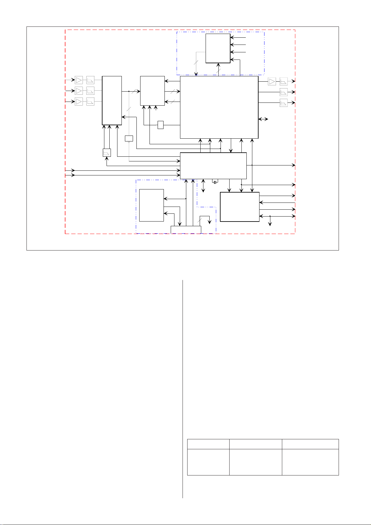
12
Feature box
DB711 / 710 / 700
Y
U
V
VSA / VSYNC1
HSA / HSYNC1
A/D-C
YUV
INIT,CLP
CLK
A/D-C_REFV
Y
8
&
12
RSTR
FM1
3 Mb
ENW
ENR
RSTW
SWCK
SRCK
CLK
&
27 MHz
13.5 MHz
EEPROM
VCLK
DDC1
interface
SDA
SCL
In DB700 only
In DB700 and
DB710 only
FM_RST
12
2
CLK13.5_I
D0...D11_FM1
FM1_ENW
FM1_ENR
FM1_RSTW
OVFL
PWM_REF
VSYNC1
HSYNC1
HSYNC
VSYNC
VGA
YUV
12
IIC-bus
3
VS_50
CLK27_I
RGB VGA
to Xtpp
SWCK
FM2
SRCK
3 Mb
RSTW
RSTR
YUV
12
IQTV2.1
DB711
UP-C, HFC, HEQ
CTI, LTI, Peaking
D/A-C
DB700/710
UP-C, FC, NR, HEQ
CTI, LTI, Peaking,
D/A-C
HS_IPLL
CLK_IPLL
DPLL1.02
27 MHz
27 MHz
LLC
Deflection
controller
FM2_ENW
FM2_ENR
VS_50_100
CLK
VA
VA HA
CLK_OPLL
VS_50_100
FM_RST
AY
AU
AV
CLK_OPLL
IIC-bus
HS_OPLL
HSYNC_O
VSYNC_O
DSC
EHT, HFB
HD, VD, EW
IIC-bus
IIC-bus
Block diagram of the Feature boxes DB711, 710 and 700
Feature-Box DB710
Die Grundfunktionen der DB710 entsprechen im Prinzip
denen der DB711. Dereinzige sichtbare Unterschied ist die
Ausstattung der DB710 mit zweiFeldspeichern, FM1 und
FM2. Dieses ermöglicht Rauschreduzierung
undVertikalzoomfunktionen (Umwandlung des
Vertikalformates).
Die Aufwärtsumwandlung von 50 auf 100 Hz in der DB710
beruht auf einer Mittelwertinterpolationsrate, die Bild- und
Zeilenflimmern reduziert. ImMittelwert-Filterverfahren wird
ein 7-Punkt-adaptiver Mittelwertinterpolatorverwendet,
dessen Abtastfenster aus 7 Abtastwerten besteht, die in
horizontaler, vertikaler undzeitlicher Richtung
abgenommen werden. Der 7-Punkt-Mittelwertausgang
wirddurch einen 3-Punkt-Vertikalmittelwertausgang ersetzt,
wenn einDifferenzsignal den extern bestimmten
Schwellenwert überschreitet.
Das Rauschreduziersystem besteht aus einem adaptiven
Mittelwert-Nachfilter,der auf einem sogenannten
bewegungsadaptiven, zeitlich rekursiven und
mittelwertbildenden Filter basiert. Das System dient nicht
nur zurRauschreduzierung, sondern es vermindert auch
Überlappungseffekte. Die Rauschreduzierung bezieht
Bauteilefür Luminanz und Chrominanz ein. Wie oben
erwähnt, erfordert die Funktion derRauschreduzierung
einen zusätzlichen Feldspeicher. Dieser Feldspeicher FM2
istmit dem FM1 identisch und ist auf ähnliche Weise mit
dem IQTV2-Schaltkreisverbunden.
Die Eigenschaften der Vertikalformatumwandlung des
IQTV2-Schaltkreisesermöglichen die Darstellung aller
Vertikalzooms mit einer vollenVertikalauflösung von 576
aktiven Zeilen. Dieses Geschieht aufgrund derdigitalen
Signalverarbeitung und der linearen Vertikalinterpolation.
Feature-Box DB700
Die funktionalen Features sind ähnlich wie bei der
DB710,Zwischenwertinterpolation, Rauschreduzierung,
volle Vertikalauflösung usw.Zusätzlich zu diesen Features
ist die DB700 mit einer VGA-(Video GraphicsArray)
Schnittstelle ausgestattet, um die Benutzung des
Fernsehgerätes als PC-Monitor zu ermöglichen. Aus
diesemGrund wird ein zusätzlicher Speicherschaltkreis
benötigt. DerSpeicherschaltkreis ic3 ist ein serieller
EEPROM, der mit den nötigen Datenfür eine automatische
Konfiguration der Bildschirmsteuerung des Computers
über denBildschirmdatenkanal 1 (DDC1) vorprogrammiert
ist.
Die vertikalen und horizontalen Synchronsignale vom VGAAnschluß werden überinvertierende Schmitt-Trigger und
weiter an die Pins 27 (vert sync) und 24/26(hor sync) des
DPLL1 geleitet.
Die analogen RGB-Signale werden ohne jede Verarbeitung
durch das Modul überden Anschluß Xtpp, oder über das
Bild-in-Bild-Modul (falls vorhanden) auf derHauptplatine
zum RGB-Videoprozessor geführt. Werden auch Tonsignale
am PCabgenommen, werden diese über den Scart3 und
das VGA-Audiomodul TA710 eingegeben.
Die folgenden Betriebsdaten des VGA sind
verfügbar:
Auflösung Zeilenfrequenz Feldfrequenz
640 x 480 31,5 kHz 60 Hz
640 x 350 31,5 kHz 70 Hz
640 x 400 31,5 kHz 70 Hz
Page 49
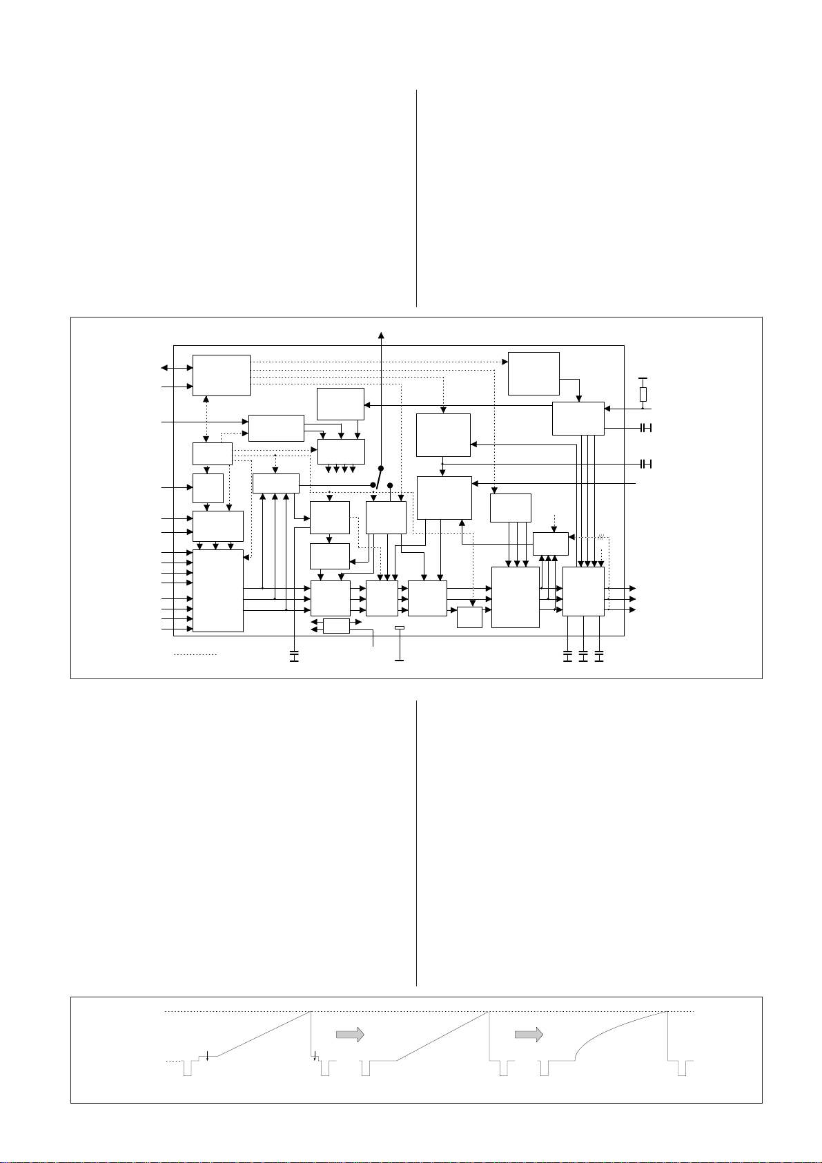
13
e
g
RGB Video Processor TDA4780, ICt1
Allgemein
Der Schaltkreis TDA4780 ist ein RGB-Videoprozessor mit
einer automatischenAbschaltsteuerung, Gamma-Korrektur,
dynamischer Schwarzsteuerung und BlueStretch.
Der Schaltkreis enthält eine Linearmatrix, um die LuminanzundFarbdifferenzsignale in RGB-Signale umzuwandeln. Der
Prozessor ist auch in der Lage, zwei externeRGB-Signale
zu verarbeiten. Alle Parameter und Funktionen werden über
den IIC-Bus gesteuert.
Y
27
28
14
8
10
11
12
13
7
6
2
3
4
1
2
I C-bus
interface
Control
registers
0.45V/
1.4V
VBS
PAL/SECAM
NTSC
Matrix
Fast
signal
switch,
blanking
IIC bus data
and control
TDA4780
Sandcastle
detector
Y-Matrix
R
G
B
18
1st and 2nd
switch on
delays
Timin g
generator
Timing pulses
Adaptive
black
control
Gamma
adjust
Saturation
adjust
Supply
Peak dark
storage
SDA
SCL
Sandcastle
Y
V
U
R
G
B
Fsw
R
G
B
Fsw
Signalschalter
Schnelle Signalquellenschalter wählen die RGB-Signale aus
einer von dreiMöglichkeiten für Eingangssignale: Die
Matrixstufe, der Videotextschaltkreisoder das Bild-in-BildModul. Diese Wahl wird über den IIC-Bus oder durch
dieSchnellaustastsignale FB an den Pins 1 und 13 gesteuert.
Während der vertikalen undhorizontalen Austastzeit wird
ein künstlicher Schwarzwert eingesetzt, um
dieSynchronimpulse des Luminanzsignales zu begrenzen,
um Brummen während derAbschaltmeßzeit zu
unterdrücken und um Rauschen während dieser Intervalle
zu eliminieren.
Y-Matrix und adaptiver Schwarzwert, GammaKorrektur und Sättigungssteuerung
Die Sättigungssteuerung wird durch Variieren der Amplitude der RGB-Signalerelativ zur Amplitude der
Luminanzsignale durchgeführt. Aus diesem Grunde muß
das Luminanzsignal in der Y-Matrix aus den RGBSignalenneu erzeugt werden.
Nach der Y-Matrix wird das Luminanzsignal
26
Y
(Hue)
D/A
converters
Contrast
adjust
5
+8V
Funktionsbeschreibung
Signaleingangsstufen
Die Luminanz- und Farbdifferenzsignale aus dem FeatureBox-Modul werden an denPins 8 (Y), 6 (U) und 7 (V)
eingegeben. Der Eingangspegel für dieLuminanzsignale
(0,45 Vpp oder 1,4 Vpp) ist über den IIC-Bus (Pins 27 und
28) wählbar. In diesem Fall beträgt Vpp 1,4 V. Die Signale
werden zur Linearmatrixstufe geleitet, umsie in RGBSignale zu wandeln.
Die RGB-Signale aus dem Videotext-Schaltkreiswerden an
die Eingangspins 2 (R), 3 (G) und 4 (B) geleitet. Die RGBSignale aus dem Bild-in-Bild-Modul (oder aus dem VGAAnschluß) werden zu den Eingangspins 10(R), 11 (G) und
12 (B) geleitet.
Alle Eingangssignale werden geklemmt, um die gleichen
Schwarzwerte amSignalschalteingang zu erhalten.
3x6-bit
reference
registers,
MUX, DAC
Peak drive
limiter,
6-bit D/A
converter
Averag e
beam and
peak drive
limiting
Brightness
adjust
9
Ground
R
G
Blue
stretch
PDL
3x6-bit
DAC
Blanking,
measurement pulse
insertion,
white point
adjust
Cut-off
comparators
Peak
detector
Cut-off storage
Cut-of f
adjust,
output
stages
21
B
23 25
R
G
zurSteuerungsstufe für den adaptiven Schwarzwert geführt.
Dieses ermittelt dieniedrigste Spannung der
Luminanzkomponente des internen RGB-Signals während
der Abtastzeit undbringt diese auf den nominalen
Schwarzwert. Um den nominalen Weißwert konstantzu
halten, wird gleichzeitig der Kontrast erhöht. Dieser
Vorgang erweitert dendynamischen Bereich des
Kontrastes.
Nachfolgend wird das Luminanzsignal in der GammaKorrektur verarbeitet. Diesebesitzt eine nicht-lineare
Übertragungscharakteristik. Die Gamma-Korrekturverstärkt
die unteren Werte des Signals mit einen höheren
Verstärkungsfaktor.Dieser Prozeß verbessert die Trennung
der dunklen Bildflächen von den anderenBildflächen.
Schließlich wird das Luminanzsignal zur Steuerungsstufe
der Farbsättigung geleitet.
Das Y-Signal wird zusätzlich zur Steuerungsstufe für den
adaptiven Schwarzwertdurch einen internen Schalter zum
Ausgangspin 26 und weiter zum SVM-Modulgeleitet.
Die Gamma- und Sättigungseinstellungen werden über den
IIC-Bus gesteuert.
19
17
16
15
24
22
20
Leakage
and cut-off
current
input
Leakage
storage
Peak drive
limiting storag
Averag e
beam current
R
G
B
Nom white
level
Nom black
level
Input si
nal Adaptive Black level Control Gamma Adjust
Principle of the adaptive black control and gamma adjust
Page 50

14
Kontrast- und Helligkeitsregelung
Beide Einstelleinheiten bestehen aus elektronischen
Potentiometern und werdenüber den IIC-Bus gesteuert. Die
Kontrastregelung hat Einfluß auf die Amplitudedes RGBSignals, wobei die Helligkeitsregelung Einfluß auf den DCWert desRGB-Signals relativ zum Schwarzwert hat.
Blue Stretch
Der Blue Stretch-Kanal ermöglicht eine zusätzliche
Verstärkung, wenn dasBlausignal größer als 80% der
nominalen Signalamplitude ist. In solchen Fällenwird der
Weißpunkt auf eine höhere Farbtemperatur gebracht, so
daß weißeBildflächen scheinbar heller sind.
Meßimpulseinfügung und Austasten
Während der horizontalen und vertikalen Austastzeit sowie
der Meßdauer werdendie Signale auf einen
Ultraschwarzwert ausgetastet, so daß der der Leckstromder
Bildröhre gemessen und automatisch kopensiert werden
kann.
Die Meßimpulsewerden im Taktgenerator erzeugt und über
die Leitung 20 in den R-Kanal eingegeben; derzweite wird
über die Leitung 21 in den G-Kanal eingegeben und der
dritte überdie Leitung 22 in den B-Kanal eingegeben. Diese
Meßimpulse werden mit denRGB-Signalen zu den
Videoausgangsvertärkern (ICh1, ICh2 and ICh3) geleitet und
leitendie Spannungspegel an Pin 19 zurück. Während der
Abschaltmeßzeilen sind dieAusgangssignalpegel auf dem
Abschaltmeßpegel. Die vertikale Austastdauer wirdmit
einem Sandcastle-Impuls getaktet. Die Meßimpulse werden
durch die negativ verlaufendeFlanke im Vertikalimpuls des
Sandcastle-Impulses ausgelöst und starten nachdem
folgenden Horizontalimpuls.
Weißpunkteinstellung, automatische
Abschaltesteuerung und Ausgangsstufen
Die nominale Signalamplitude kann um ±50% durch die
Weißpunkteinstellung überden IIC-Bus variiert werden.
Während der Verluststrommessung wird der
Verlustkompensiert, um eine Referenzspannung am
Abschaltmeßeingang an Pin 19 zuerhalten.Dieser
Kompensationswert wird im externen Kondensator an Pin
17 gespeichert.Während der Abschaltstrommessung der
R-, G- und B-Kanäle wird die Spannung andiesem Pin mit
der Referenzspannung verglichen, die über den IIC-Bus für
jedenFarbkanal individuell einstellbar ist. Die so
abgeleiteten Steuerspannungen werden inden externen
Gegenkopplungskondensatoren an den Pins 21, 23 und
25gespeichert. Schaltstufen addieren diese Spannungen
zu den entsprechendenAusgangssignalen. Schließlich
werden die RGB-Signale auf den Nennwert von 2 Vpp
verstärkt und anden Pins 24 (R), 22 (G) und 20 (B)
ausgegeben.
Strahlstrom und Steuerspitzenbegrenzung
Im Schaltkreis sind zwei Arten von Signalbegrenzern
vorgesehen. Es gibt einenMittelwert-Strahlbegrenzer,
derden Signalpegel reduziert, wenn ein bestimmter
Mittelwert überschritten wirdund ein
Steuerspitzenbegrenzer, der aktiviert wird, wenn eines der
RGB-Signaleauch nur kurz den vom IIC-Bus bestimmten
Schwellenwert überschreitet. DieStrahlstromBegrenzungsspannung wird an der
Kathodenstrominformation abgelesen und überdie
Transistoren tt4 / tt1 und den Kondensator Ct29 zu Pin 15
geleitet. Wenndie Spannung an Pin 15 wegen der
Aufladung von Kondensator Ct29 auf unter +4 Vabfällt,
beginnt der interne Begrenzer den Kontrast zu reduzieren.
Wenn die Spannungauf unter + 2,8 V abfällt, beginnt der
Begrenzer auch die Helligkeit zureduzieren.
Impuls in kombinierte Zeile, Feldimpulse und
Klemmimpulse auf, diezum Taktgenerator geleitet werden.
Der Taktgenerator enthält einen Zeilenzähler, der
dieAustast- und Meßimpuls-Einsatzstufen steuert.
Einschaltverzögerungs-Schaltkreis
Nach dem Einschalten werden alle Signale ausgetastet und
einAufwärm-Testimpuls wird während der AbschalteMeßzeilen an die Ausgängegeleitet. Wenn die Spannung
am Abschalte-Meßeingang einen internen
Pegelüberschreitet, wird die Abschaltsteuerung aktiviert,
jedoch wird das Signal noch ausgetastet. Die
Signalaustastung wird gestoppt, wenn sich die
Abschaltsteuerung stabilisierthat.
CRT-Modul
Videoausgangsverstärker ICh1, ICh2 und Ich3
Die Videoendstufe besteht aus drei separaten
Ausgangsverstärkern, TDA6111. Der Schaltkreis besitzt eine
hohe Anstiegsgeschwindigkeit und eine große Bandbreite
von 16 MHz und ist daher für den Einsatz bei 100 Hz
geeignet. Der Schaltkreis ist gegen KathodenstrahlröhrenFlashover und elektrostatische Entladung (EGB) geschützt.
Die RGB-Signale vom RGB-Videoprozessor werden über
Tiefpaßfilter zuminvertierenden Eingangspin 3 der
Verstärker geführt. Die nicht-invertierenden Eingangspins
1 sind an einen Spannungspegel von +3 V verbunden. Die
Verstärkerhaben zwei Ausgänge für die
Bildröhrenkathoden, den Pin 8 für die Gleichströme und
Pin 7 fürdie Übergangsströme. Nach diesen Ausgangspins
werden die verstärktenRGB-Signale zu den
Bildröhrenkathoden geleitet. Die
Gegenkopplungsinformation wird an Pin 9 ausgegeben und
über einen Widerstand an den Eingangspin 3 abgegeben.
DieKontrolle des Schwarzwertes der Kathoden wird über
die Ausgangspins 5durchgeführt. Diese Ausgänge sind
über Widerstände miteinander verbunden unddas
Endergebnis wird zum RGB-Videoprozessor an die Pins 19
(Abschaltsteuerung) und Pin 15(Strahlstrom) geleitet. Die
erforderlichen Versorgungsspannungen werden zu den
Pins 2 (+12 Vp) und 6 (+200 V) geleitet.
Ein negativer Rückschlagimpuls vom
Diodenspalttransformator Mk1 (DST) wird zum
Schirmgitter G1 über den Anschluß Xh1, den Kondensator
Ch19 und den Widerstand Rh28 geführt. Dieses verstärkt
die horizontale Austastung während des Zeilenrücklaufs.
Die Ausblendung des Bildschirms nach dem Ausschalten
wird von den Transistoren Th1 und th2 durchgeführt.
Während des normalen Betriebs wird derKondensator Ch27
auf +12 V und der Kondensator Ch18 auf +200 V
aufgeladen.Wenn das Fernsehgerät ausgeschaltet wird,
entlädt sich Ch27 an der Basis von Th1. Der Transistorleitet
und entlädt Ch18 als negative Ladung auf das Schirmgitter
G1. Ebenfallswird der Kondensator auf +12 V geladen.
Wenn das Fernsehgerät ausgeschaltetwird, geht die Basis
von th2 auf LOW und der Transistor leitet. Ch28 entlädt
dennicht-invertierenden Eingangspin 1 augenblicklich und
+200 V werden an dieAusgänge geleitet. Dieses verhindert
das Steigen des Strahlstroms, bis Th1ausreichend Zeit
hatte, die Bildröhre zu spe!rren.
Sandcastle-Detektor und Taktgenerator
Der zweistufige Sandcastle-Impuls (DSC) von der
Ablenksteuerung derFeature-Box wird zu Eingangspin 14
geführt. Der Sandcastle-Detektor teilt denSandcastle-
Page 51
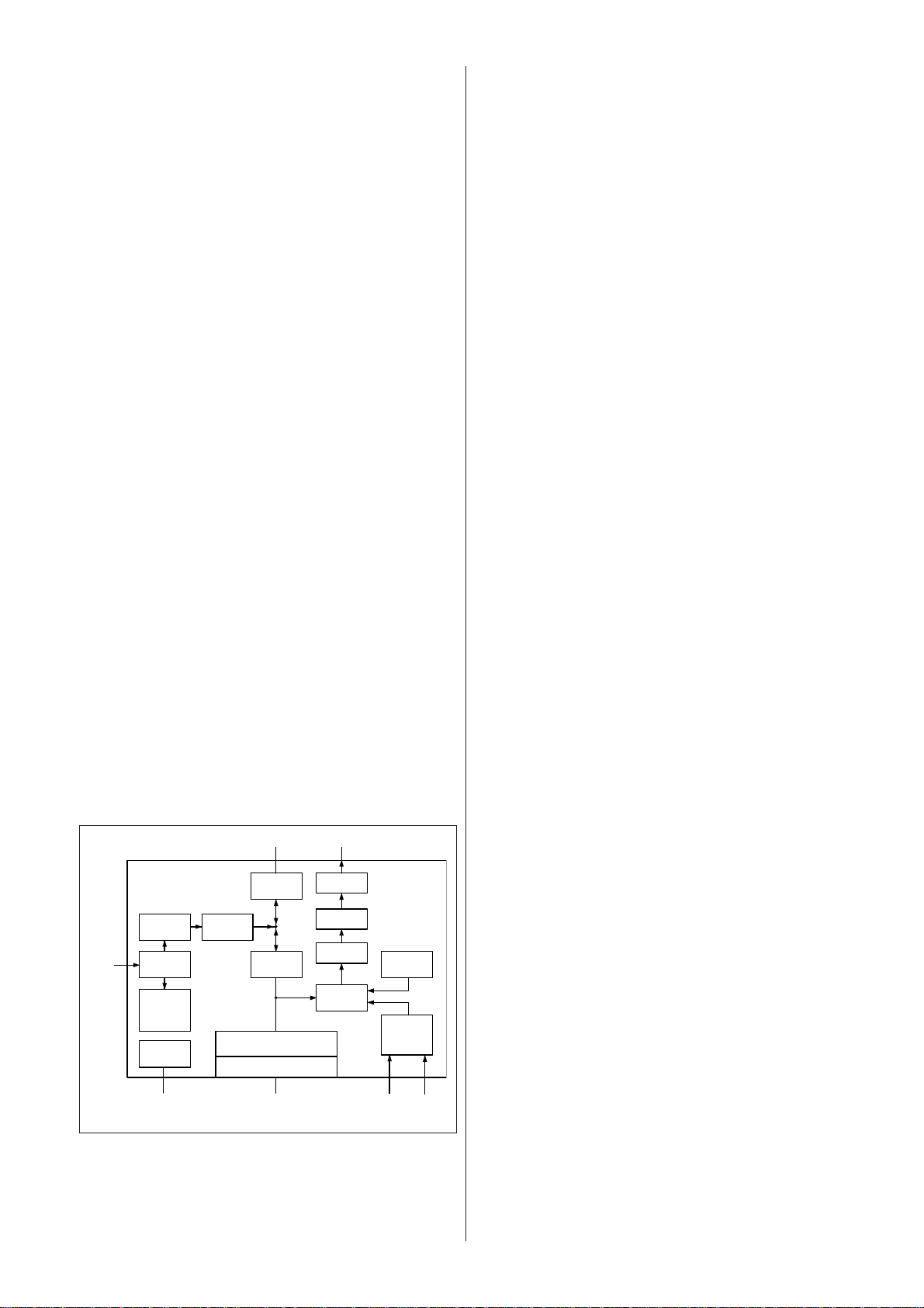
Videotext
y
Megatext SDA5273, Icr1
Der SDA5273 Megatext-Schaltkreis ist ein einziger Chip,
der eine Kombinationaus Data Slicer, Videotextprozessor,
Seiten- / Pixelspeicher und Displaysteuerung ist. Digitale
Signalverarbeitung wird verwendet, um externe diskrete
Bauteile zu vermeiden.
Der Speicher kann durch die Verwendung eines externen
DRAM erweitertwerden, um die Leistungsfähigkeit des
Videotextes zu erhöhen.
Die Multistandard fähigkeit des Megatext-Schaltkreises
stellt die Eignung füralle Länder sicher, die den „World
System Teletext” (WST) Level 1.5 übertragen.
Die Megatext-Schaltkreisfunktionen sind das Entschlüsseln
und die Darstellungvon Videotextinformationen aus einer
analogen Quelle, die CVBS-Eingabe und die Erzeugung der
Displays, die dem Fernsehbenutzer Statusinformationen
oder Hilfestellung geben. Der RGB-Ausgang des MegatextICs ist mit dem RGB-Eingang des RGB-Videoprozessors mit
Schnellaustastinformationen verbunden.
Der Megatext-IC wird über den M3L-Bus gesteuert, der eine
maximale Daten übertragungsrate von 1 Mbit/s aufweist.
Schaltkreisbeschreibung
Das CVBS-Signal von der Videomatrixschaltung wird zu
Eingangspin 9 geführt.
Das Grundprinzip der Signalverarbeitung wird unten im
Blockschaltbild gezeigt.
Die analogen RGB-Signale und Schnellaustastsignale
werden an den Pins 44 (R),45 (G), 46 (B) und 47 (FB)
ausgegeben. Der vertikale Synchronimpuls (2V) wirdzu Pin
3 und der horizontale Synchronimpuls (2H) zu Pin 4 geleitet.
DieSynchronimpulse werden der Feature Box entnommen
(VDFL und HDFL).
Ein externer Quarz mit 20,48 MHz befindet sich zwischen
den Pins 5 und 6. Die Pins 18...35 und 37 sind Addresse
und Datenleitung für den externen DRAM (icr2). Die
Versorgungsspannung +5 Vr wird an die Pins 10, 11, 13, 15
und 17geleitet. Ein hoher Pegel an Pin 14 verursacht ein
Zurücksetzen des Microcontrollers.
Eine stabilisierte Referenzspannung von 3,3 V für interne
Verwendung von derZenerdiode Zdr1 wird zu Pin 16
geleitet.
Der Megatext-Schaltkreis kommuniziert mit dem
Microcontroller unter Verwendungder Pins 49 (SCL), 50
(SDA) und 51 (IICENable) über den M3L-Bus.
15
Data Slicer trennt die Videotextdaten vom
digitalisierten CVBS-Signal.
Akquisitionsschnittstelle
synchronisiert die Bytes, wandelt
serielle Bits zuparallelen Bytes und
ermittelt den Rahmencode.
Prozesseinheit steuert die Austauschfunktionen
zwischen Akquisition,Speicher, Display und Bus-Schnittstelle.
Interner Speicher Interner 44 Kbyte DRAM.
Ext. DRAM-Schnittstelle
Schnittstelle zwischen Megatext und
externem DRAM.Display-Generator
steuert den Datentransfer vom IRAM
zum DG, entschlüsseltdie
Displaywörter, steuert die
Displayformate und erzeugt spezielle
Cursor.
ROM-Zeichen Zeichenpixelspeicher.
CLUT Farbsuchtabellen.
Display-Takt und Taktgeber
erzeugt die horizontalen Taktsignale
für dasDisplay und einen
zeilengekoppelten Displaytakt.
FIFO Steigert die Pixelwiederholrate von
normalerweise 24 MHz auf 32 MHz
bei16:9 Format.
D/A-Wandler Erzeugt analoge RGB-Signale.
Bus-Schnittstelle M3L-Bus-Schnittstelle zwischen
Megatext undMicrocontroller.
Megatext Plus SDA5275, Icr1
Der Megatext Plus SDA5275-Schaltkreis basiert auf dem
MegatextSDA5273-Schaltkreis. Der Hauptunterschied
besteht in der internenDatenverarbeitung, welche die
Videotextdatenverarbeitung in Übereinstimmungmit dem
Level 2.5 ermöglicht. Der Level 2.5 erzeugt weitaus bessere
Graphiken (Bitmap-Graphiken), mehr Farben(4096) und
eine Erweiterung für das 16:9-Format, die eine
breitereDisplayseite ermöglicht. Daher kann der Level 2.5
56 Zeichen auf jeder der 25Zeilen darstellen (1400 Zeichen
/ Seite). Der Level 1.5 kann nur 40 Zeichen pro Zeile
darstellen(1000 Zeichen / Seite).
Aufgrund von Seiten mit höherem Level erfordert
derMegatext Plus-Schaltkreis stets eine externe
Speicherschaltung.
M3L-Bus RGB
CVBS
SDA 5273
Data
Slicer
A/D
Converter
Sync
Slicer &
Timing
Crystal
Oscillator
20.5 MHz
Cr
stal
Interface
Bus
Interface
Acq
PU
24-KByte DRAM
External DRAM-Interface
to external
DRAM
DAC
FIFO
CLUT
Display
Generator
Character
ROM
Display
Clock &
Timing
2V
2H
A/D-Wandler wandelt das CVBS-Signal in einen 7-
Bit Binärcode.
Sync Slicer und Takt trennt die horizontale/vertikale Syn-
chronisation vom digitalisierten
CVBS-Signal und erzeugt einen
zeilengekoppelten 24MHzAkquisitionstakt.
Videotextspeicher DRAM, icr2
Der externe Videotextspeicher ist ein 4 Mbit großer,
schnellerDirektzugriffsspeicher (DRAM). Er ist als 1 048 576
Vier-Bit-Worte aufgebaut(4 194 304 Bit). Der Schaltkreis
arbeitet nach der CMOS-Silicon Gate-Technologie.
Eine Teletextseite benötigt 1 Kbyte (8192 Bit) an
Speicherplatz, so daß derSchaltkreis theoretisch 512
Videotextseiten (4 194 304 : 8 192 = 512) speichern kann.
Dieses reduziert die Seitenzugangszeit virtuell auf
Null.Während des ersten Übertragungszyklus der
Teletextseiten wird derSpeicherschaltkreis für die
übertragenen Seiten formatiert.Während des zweiten
Übertragungszyklus werden die übertragenen Seiten
imSpeicher abgelegt.
Page 52

16
STEUERUNGSSYSTEM
Das Steuerungssystem besteht aus den folgenden
Schaltkreisen:
- Programmspeicher, Icf1
- NV RAM, Icf2
- Microcontroller, icf3
- AND-Gatter, icf4
- RESET-Schaltkreis, icf5
- Fernbedienung und Bedienteil am Fernsehgerät
Programmspeicher, Icf1
Abhängig von der Version des Fernsehgerätes kann das
Chassis entweder miteinem 4 Mbit- oder 8 MbitProgrammspeicher ausgestattet sein. Beides sindschnelle,
durch UV-Licht löschbare und programmierbare
Festwertspeicher (EPROM). Später kann auch ein einmal
programmierbarer (OTP) Festwertspeicher oder ein
normaler Festwertspeicher verwendet werden.
Der 4 Mbit (512 kbyte)-Speicher ist als 524 576 Acht-bitWörter strukturiert.Der Microcontroller addressiert diesen
Speicher über die AdressenleitungenA0...A18.Der 8 Mbit
(1024 kbyte)-Speicher ist als 1 048 576 Acht-bitWörterstrukturiert. Dieser Speicher erfordert eine
zusätzliche Speichererweiterung.Diese wird von icf4
ausgeführt, die den Adreßraum in vier getrennte
Blöckeaufteilt, Datenbank 0, 1, 2 und 3. Die Systemsoftware
ist in den Datenbanken 0 und 1 programmiert.Die
Datenbanken 2 und 3 werden für den Menütext und die
Bildschirmbedienerführung (EUM) benutzt.
Der Programmspeicher kommuniziert mit dem
Microcontroller über den Adressen-und Datenbus.
NV RAM, Icf2
Der NV-Direktzugriffsspeicher (NV RAM) ist ein Low Power
16 kbit, elektrischlöschbarer und programmierbarer
Festwertspeicher (EEPROM). Er ist in 8getrennte
Adreßblöcke aufgeteilt, von denen jeder aus 256 Acht-bitWörternbesteht (8 x 256 x 8 = 16 384 bits). Die Daten werden
über den IIC-Bus übertragen.
Einstellungen, die im NV RAM gespeichert werden können,
umfassen InformationenÜber Fernsehprogramm
speicherplätze, über den IIC-Bus gesteuerte
Serviceeinstellungen, Standardeinstellungen,
Benutzereinstellungen, Options-und Konfigurationsdaten
sowie gespeicherte Videotextseiten.
Microcontroller, icf3
Der SDA30C264 ist ein Low Power CMOS-Schaltkreis, der
einenAcht-bit-Prozessor, einen 2048 byte + 256 byteDatenspeicher (RAM), einenOszillator und Taktschaltungen,
zwei 16-bit Timer / Zähler und einenÜberwachungstimer
enthält. Der Microcontroller ist mit dem
Programmspeicherüber den Adressen- und Datenbus und
mit anderen Schaltkreisen über den IIC-Busverbunden.
Abhängig von der Größe des Programmspeichers (4Mbit
oder 8Mbit) und desBildseitenverhältnisses (4:3 oder 16:9)
sind manche Bauteile (sowie Gattericf4 und einige Jumper)
entweder eingebaut oder weggelassen worden.
Darausergeben sich verschiedene Funktionen an manchen
Pins des Microcontrollers.
Die mit einem * markierten Pins werden nach der
Pinkonfigurationstabelledetailierter beschrieben.
Pin configuration of the microcontroller SDA30C264
Pin Beschreibung
1 Eingang Kopfhörerschalter, Kopfhörer angeschl. =
HIGH
2 AV-Verbindungsdaten zu Scartpin 10, hohe Impulse
3 * 4Mb/4:3 : TA700-Status Eingang, Stecker
angeschlossen = HIGHAlle 8Mb und alle 16:9 :
Ausgang Bildneigung, 0...5 V
4 M3L-Bus, Megatext ermöglichen, ermöglichen =
LOW
5 Einstellung Horizontallage in VGA-Geräten (PWM -
> Xo3-1 = 0...5 V)
6 * 4Mb/4:3 : Eingang RGB-Status, Status ein =
HIGHAlle 8Mb und alle 16:9 : RGB-Status ein = HIGH
/ TA700-Status ein, Steckerangeschlossen = HIGH
7 Vom Serviceanschluß gehalten, gehalten = LOW
8 * Bank 1 / Steuerung zu EPROM-Datenbankwahl
(8Mb)
9 * Bank 0 / Steuerung zu EPROM-Datenbankwahl
(8Mb)
10 Masse
11 Versorgungsspannung, +5 Vstb
12...13 Quarz 12 MHz
14 RESET Eingang, RESET bei LOW
15 Nicht angeschlossen
16...28 Adressenbus für Programmspeicher (EPROM)
29...36 Datenbus für Programmspeicher (EPROM)
37...39 Adressenbus für Programmspeicher (EPROM)
40 Masse
41 Versorgungsspannung, +5 Vstb
42 Adressenbus für Programmspeicher (EPROM)
43 EPROM-Datenbanksteuerung (8Mb). LOW =
Datenbank 0, HIGH = Datenbanken 1, 2 und 3
44 IIC-Bus, serieller Takt
45 IIC-Bus, serielle Daten
46 Aufnahme-LED ein bei LOW / Bedieneinheit liest
Ausgangsimpuls (Eingang an den Pins 61 oder 62)
47 * Multistandard-ZF = Ausblendimpuls (LOW) für
DatenspeicherKeine Multistandard-ZF = APSi-
Filtertreiber, APSi bei HIGH
48 P_on, Bild „Ein”-Spannungen bei LOW
49 * R_on, Aufnahmespannungen bei LOW
50 * RESET-Impuls (HIGH) für MSP / Subwoofer-
Identifizierung = LOW
51 * Stummschaltung bei HIGH / Identifizierung von 16:9
(niedrigere Spannung), 4:3(höhere Spannung)
52 * Identifizierung von Scart 3 / Status ein (aus = 0 -
1,2V, 16:9 = 1,3 - 3,2V,4:3 = 3,3 - 5V) 53...54Scart 1, 2
Status ein (aus = 0 - 1,2V, 16:9 = 1,3 - 3,2V, 4:3 = 3,3
- 5V)
55 Identifizierung der Version des ZF-Moduls. Ablesen
an Widerstand R556 (Multi)/ R526 (Nicht-Multi)
56 GND
57 Adresse für Programmspeicher (EPROM)
58 Referenzspannung der internen D/A-Wandler
59 M3L-Bus, Takt für Megatext
60 M3L-Bus, Daten für Megatext
61 Bedieneinheit 2 Eingang
62 Bedieneinheit 1 Eingang
63 AV-Verbindung Dateneingang von Scartpin 10,
niedrige Impulse
64 Eingang Fernbedienung, hohe Impulse
Page 53

Die folgende Liste enthält genauere Informationen über
jeden mit * markiertenPin.
3 a) Bei 4:3 Fernsehgeräten mit einem 4 Mbit
Programmspeicher gibt der Pin 3die Statusinformation
(Status Ausgangsleitung) vom einstellbaren
Audiomodulein. Er zeigt an, ob das Modul benutzt oder
nicht benutzt wird, d.h., ob derStecker angeschlossen
oder nicht angeschlossen ist.Wenn der Stecker
angeschlossen ist, leitet der Transistor ta9 nicht und
derPin 3 ist auf HIGH. Dieses aktiviert eine Auswahl
von drei Stummschaltungsarten: 1) TV-Lautsprecher
werden stummgeschaltet, 2)TV-Lautsprecher und
einstellbares Audiomodul werden stummgeschaltet
oder 3) keine Stummschaltung. Der Schaltkreisicf4 ist
nicht installiert und die Verbindung zur
Bildneigungseinstellung istnicht angeschlossen. b )
Bei allen 16:9 Fernsehgeräten und allen mit 8 Mbit
Programmspeicher gibtder Pin 3 eine
Bildneigungseinstellung aus. In diesen Fällen
sindInformationen aus dem Audiomodul nicht
verfügbar. Mit derBildneigungseinstellung kann die
Deklination des Bildes kompensiert werden, die durch
das magnetische Feld der Erdeverursacht wird.
Abhängig von der Steuerspannung steuern die
Transistoren tt5,tt6 und tt7 die Spannung entweder von
+12 V über die Löschspule auf +5 V(niedrige
Steuerspannung, tt6 leitet) oder von +5 V über die
Löschspule an Masse (hoheSteuerspannung, tt5 und
tt7 leiten).
6 a) Bei 4:3 Fernsehgeräten mit 4 Mbit
Programmspeicher dient der Pin 6 als Anzeige des
RGB-Status (rf51 ist installiert). Wenn der RGBAnschluß benutztwird, leitet der Transistor tq4 nicht
und der Pin 6 ist HIGH.
b) Bei allen 16:9 Fernsehgeräten und allen mit 8 Mbit
Programmspeicher dientder Pin 6 als Anzeige des RGBStatus (= Scartpin 16 ist HIGH) und desTA700-Status
über icf4 (rf51 ist nicht installiert).Die Software
überprüft den Status in bestimmten Zeitabständen,
indem sie einenhohen Pegel von µC Pin 9 zu icf4-4 an
Pin 13 zuführt. Wenn bei icf4-4 der Pin12 HIGH ist (RGBStatus ein), führt der Pin 11 einen hohen Pegel an µC
Pin 6zu.
Das gleiche Überprüfungsverfahren gilt auch für den
TA700-Status, jedochbenutzt dieser den µC Pin 8 und
den icf4-3. Während dieser Überprüfung ist derµC Pin
43 (A18) immer LOW. Das bedeutet, daß die Pegel an
den Pins 8 und 9 keinen Einfluß auf die
Datenspeicherung des EPROM haben.
8/9 Wenn der µC Pin 43 HIGH ist, wählen diese Pins über
icf4-1 und icf4-2 diebenötigte Datenbank 1, 2 oder 3.
Wenn der µC Pin 43 LOW ist, ist nur dieDatenbank 0 in
Gebrauch. Daher haben die Pins 8 und 9 keinen Einfluß
auf dieDatenspeicherung, sie können jedoch für andere
Funktionen benutzt werden.
43 Der Pin 43 ist eine Adressenleitung, die zur
Datenspeicherung des 8 MbitProgrammspeichers
verwendet wird. Wenn der Pin LOW ist, wird die
Datenbank 0gewählt; ist der Pin HIGH, werden
entweder 1, 2 oder 3 gewählt. Bei dem 4 MbitSpeicher
ist der Pin 43 eine normale Adressenleitung (A18).
47 a) Bei Multistandard-Fernsehgeräten übermittelt der
Pin 47 einenAusblendimpuls (LOW) für das
Schieberegister auf dem ZF-Block.
b) Bei Fernsehgeräten ohne Multistandard steuert Pin
47 den SchalttransistorT501 auf dem ZF-Block.
Während der Kanalsuche (APSi) ist Pin 47 HIGH.
48/49
Die Kombination von Pegeln an diesen Pins bestimmt
den Betriebszustanddes Fernsehgerätes wie folgt:
17
48 / P_on 49 / R_on Beschreibung
H H Micropower-Betriebsbereitschaft,
Netzteil ist nicht in Betrieb
L L Fernsehgerät „ein”, Vr, Vp und
Vstb verfügbar
H L Aufnahmebetrieb, Vr und Vstb
verfügbar, Vp nicht verfügbar
L H Servicebetriebsbereitschaft, Vstb
verfügbar, jedoch weder Vr noch
Vp verfügbar
Das Fernsehgerät ist in der Servicebetriebsbereitschaft,
wenn es durch Drückender -vol / menu, TV- und i-Taste in
den Servicebetrieb gebracht wurde, jedochnoch nicht durch
zweimaliges Drücken der TV-Taste eingeschaltet wurde.
DerServicebetrieb wird genau wie der Aufnahmebetrieb
und die Servicebetriebsbereitschaftdurch die leuchtende
LED für Aufnahme angezeigt.
50 a) Während der Anlaufphase übermittelt der Pin 50
einen positivenRESET-Impuls für den Soundprozessor.
b) Durch Ablesen der Last am RESET-Impuls stellt der
Pin 50 fest, ob derSubwoofer überhaupt installiert ist.
Wenn der Subwoofer installiert ist, istauch der
Widerstand Ra107 vorhanden. In diesem Fall ist die
Amplitude desRESET-Impulses kleiner als bei nicht
vorhandenem Widerstand Ra107. Diese Überprüfung
findet inder Konfigurationsphase statt (im
Servicemodus, wenn die rote Taste gedrücktwird.
51 a) Während der Konfigurationsphase prüft Pin 51 den
Widerstand ra10 überden Transistor ta10 (b-e), um das
Bildseitenverhältnis zu erkennen. Einniedriger
Widerstand bedeutet 16:9 und ein hoher Widerstand
4:3.
b) Während des normalen Betriebes kann der
Audioverstärker durch einen hohenPegel an diesem
Pin stummgeschaltet werden (zentrale
Stummschaltung).
52 a) In der Konfigurationsphase überprüft Pin 52 die
vorhandene Installationeines Scart 3-Modules durch
Prüfung des Widerstandes ra26 (am Scart 3-Modul).
b) Pin 52 operates as a status input pin from scart 3
AND-Gatter, icf4
Das AND-Gatter dient als Funktionserweiterung bei allen
16:9 Fernsehgeräten (4und 8 Mbit Programmspeicher)
sowie bei allen Fernsehgeräten, die mit einem 8Mbit
Programmspeicher ausgestattet sind (4:3 und 16:9). In
diesen Fällen sinddie Jumper rf30 (Programmspeicher-Pin
31), rf31 (Programmspeicher-Pin1), rf48 (µC Pin3) und rf51
(µC Pin 6) nicht installiert.
Bei 4:3 Fernsehgeräten mit einem 4 Mbit
Programmspeicher ist das AND-Gatter im Gegensatz zu den
oben erwähnten Jumpern nicht installiert.
Eine detailiertere Beschreibung befindet sich bei den Pins
6, 8, 9 und 43 des Microcontrollers.
RESET-Schaltkreis, icf5
Der Microcontroller wird durch den speziellen RESETSchaltkreis icf5 (TL7705A)zurückgesetzt. Wenn das
Fernsehgerät eingeschaltet wird, übermittelt der Pin 5einen
niedrigen Pegel an Pin 14 des Microcontrollers, bis die +5
Vstb amÜberwachungspin 7 (Lesen) einen Pegel von +4,55
V erreicht.Danach dauert das Zurücksetzen für ungefähr
30 ms an. Dann geht der Pin 5 aufHIGH und der
Microcontroller wird zurückgesetzt. Die Verzögerungszeit
von 30ms beim Zurücksetzen wird durch den Kondensator
Cf21 an Pin 3 bestimmt.Wenn die +5 Vstb nur einen Moment unter den Schwellenwert von 4,55 V fällt,wird sofort
eine Zurücksetzung durchgeführt. Der Microcontroller
wirdgesperrt, was die Schaltung des Fernsehgerätes in
dieMicropower-Betriebsbereitschaft bewirkt.
Page 54

18
Fernbedienung
Die Fernbedienung arbeitet mit dem Codesystem NRC-17,
das auf einem 17-bitZweiphasencode basiert. Der
Infrarotempfänger bzw. der Verstärker Hfc1empfängt
impulsmoduliertes Infrarotlicht. Der Empfänger wandelt
dieses Lichtin ein elektrisches Signal, das demoduliert,
verstärkt und von Pin 3 aussgegeben wird. DasSignal wird
über den Transistor tfc3 an den Pin 64 des
Microcontrollersübermittelt. Während der Code
übertragung sendet der Microcontroller vom Pin 46negative Impulse. Dieses verursacht ein Aufblinken der LED Dfc4
als Hinweis für denangenommenen Code.
Bedienteil am Fernsehgerät
Das Bedienteil am Fernsehgerät umfaßt nur vier primäre
Funktionen destäglichen Gebrauchs: Lautstärke + / - und
schrittweises Programmschalten + /-. Diese Funktionen
ermöglichen die Benutzung des Fernsehgerätes ohne
dieseparate Fernbedienung. Die Informationen der
Funktionsschalter SWcf1...SWcf4 wird an die Pins 61und
62 des Microcontrollers übermittelt.
Die LED’s am Bedienteil am Fernsehgerätes zeigen den
Betriebszustand wie folgtan:
Im eingeschalteten Zustand leuchtet die grüne LED Dfc17
aufgrund der +12 Vp.In der Betriebsbereitschaft leuchtet
die rote LED Dfc16 (auf derMicropowereinheit) als Anzeige
für den vorhandenen Netzanschluß.Im Aufnahmebetrieb
leuchtet die rote LED Dfc4 aufgrund des niedrigen Pegels
anPin 46 des Microcontrollers.
Page 55
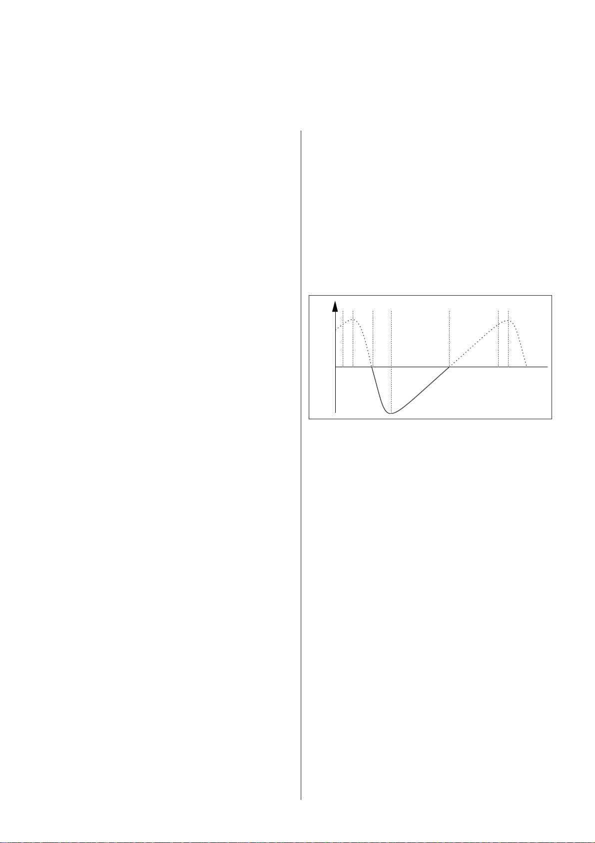
ABLENKSTUFEN
- Vertikalablenkung
- Horizontalablenkung
19
Vertikalablenkung
Der TDA8354 ist ein gleichstromgekoppelter
Vertikalablenkungsschaltkreis, dereinen einen internen
Vertikalrückschlaggenerator und eine
Schutzschaltungenthält. Die Ausgangsverstärker und der
Rückschlaggenerator werden durchHochleistungs-FET’s
angepaßt. Der IC ist thermisch geschützt und zusätzlich
gegen Kurzschlüssezwischen den Ausgängen und vom
Ausgangspin zur Masse und zurVersorgungsspannung
geschützt.
Funktionsbeschreibung
Symmetrische Vertikalimpulse vom Ablenkprozessor
TDA9151 werden über die Pins11 und 12 zu einem
stromgesteuerten Differential-Eingangsschaltkreis
geführt.Die Umwandlung von Strom zu Spannung wird
vom Widerstand rs4 über denEingangspin 3 durchgeführt.
Die Spannung an Pin 3 wird mit den Daten der
Gegenkopplung an Pin2 verglichen. Die Daten der
Gegenkopplung werden dem Ausgangsstrom durch
dieAblenkspule - gemessen über die Widerstände Rs2, Rs3
und Rs5 - entnommen.
Die Signale werden unter Verwendung eines
Vertikalsteuerschaltkreises in einer Brückenkonfiguration
verstärkt.
Die Ablenkspule befindet sich zwischen den
gegenphasengesteuerten Verstärkernan den Ausgangspins
5 und 9. Der Ausgangsstrom wird durch den Wert
desWiderstandes rs4 bestimmt. Das Widerstandsnetzwerk
(VD6xx), parallel mit derAblenkspule verbunden, dämpft
die Hochfrequenzschwingungen, die vornehmlich am Ende
derRückschlagsperiode erzeugt werden.Der zusätzliche
Widerstand rs6 an Pin 13 kompensiert die Stromdifferenzen
inden Dämpferwiderständen während der Abtast- und
Rückschlagsperiode.
Die Betriebsspannungsversorgung von +16 V an den Pins
4 und 10 sowie dieVersorgungsspannung für den
Rückschlag von +50 V an Pin 7 werden
demDiodenspalttransformator Mk1 abgenommen. Der
Betrieb mit zweiVersorgungsspannungen (Klasse G)
ermöglichen es, beide Versorgungsspannungen
unabhängig voneinander auf ihrenoptimalen Wert
einzustellen. Auf diese Art wird ein hoher
Wirkungsgraderreicht. Aufgrund der Brückenkonfiguration
ist ein Entkopplungskondensatornicht erforderlich. Daher
ist fast die gesamte Versorgungsspannung für den
Rückschlag über dieAblenkspule verfügbar.
Der Ausgang einer internen Schutzschaltung ist an Pin 1
angeschlossen. DerSandcastle-Impuls (DSC) vom
Ablenkprozessor ist ebenfalls am gleichen
Pinangeschlossen.
Die Schutzschaltung wird in möglichen Störungsfällen wie
Kurzschlüsse an denAusgangspins, bei einer offenen
Ablenkschleife oder bei einer Überhitzung desSchaltkreises
aktiviert. In solchen Fällen erhöht die Schutzschaltung
denGleichstrompegel an Pin 1 auf 2,5 V. Dieses ist der selbe
Gleichstrompegel wie derAusblendpegel des SandcastleImpulses. Somit wird ein Ausblenden desBildschirms
durchgeführt, das die Bildröhre schützt.
Horizontalablenkung
Das horizontale Steuersignal vom Ablenkprozessor wird
über einImpulsformungs-Netzwerk bestehend aus den
Transistoren tk6, Tk1, Tk2 und damitverbundenen Bauteilen
zum Steuertransformator Mk2 geleitet. Der SchaltkreisDk5,
Rk30 und Ck17 begrenzt die Schaltübergänge von Tk2. Die
Versorgungsspannung von +17 V für denTransformator
wird dem Netzteil abgenommen. Die Sekundärwicklung
desTransformators ist mit der Basis des Zeilen
ausgangstransistors Tk3 verbunden,der den Diodenspalt
transistor und die Zeilenendstufe steuert.
Die Funktionsbeschreibung der Zeilenendstufe beginnt mit
dem Zeitpunkt t5,wenn das Steuersignal negativ wird, die
Zeilenabtastperiode gestoppt wird unddie Zeilen
rückschlagperiode t1 beginnt (siehe Bild unten).
t5
t2 t4 t5 t1t3Iscan
t1
Zeilenrückschlag (t1...t3)
Aufgrund der Abschaltung des Kollektorstromes Tk3 fließt
die in derAblenkspule gespeicherte Energie am Ende der
Abtastperiode zumRückschlagkondensator Ck24. Der
Energiefluß geht bis zum Zeitpunkt t2 weiter,wenn die
gesamte Energie übertragen wurde und die
Kollektorspannung ihren Maximalwert erreicht. Der
Stromändert dann die Richtung und Energie aus dem
Kondensator fließt zurAblenkspule zurück. Zum Zeitpunkt
t3 wird der Rückschlagkondensator entladenund dabei
beträgt die Spannung 0 V. Sie wird dann negativ, wenn die
Ablenkspule durch Zuführungihrer Energie zum
Kondensator Ck27 (und Ck33) mit der Abtastperiode
beginnt.
Zeilenabtastung (t3...t5)
Zum Zeitpunkt t3, wenn die Ablenkspule mit der Zuführung
ihrer Energie zu Ck27startet, beginnt Strom über die Diode
Dk7 zu fließen. Zum Zeitpunkt t4,welcher der Mittelpunkt
der Zeilenabtastung ist, wird der Steuerimpuls an derBasis
von Tk3 wieder positiv und der Ablenkstrom kann über den
Transistor Tk3 und dieDiode Dk8 fließen. Von Zeitpunkt t4
bis t1 ändert der Ablenkstrom seineRichtung und die
Energie geht von Ck27 in die Ablenkspule. Zum Zeitpunkt
t5,dieser ist das Ende der Zeilenabtastung, wird das
Steuersignal von Tk3 negativ und dieRückschlagperiode
beginnt von neuem.
Um einen kontinuierlichen Betrieb zu gewährleisten, wird
die Energie aus dem Netzteil in der primären Wicklung von
Mk1 (Pins 6 und 3) während derAbtastperiode gespeichert,
wenn Tk3 gesättigt ist. Ein Teil dieser Energiewird zum
Ausgleich der Ablenkverluste verwendet.
Ablenkkorrekturen
Der Korrekturimpuls der Kissenverzerrung vom
Ablenkprozessor wird durch dieTransistoren ts1 und ts2
zur Basis von Transistor Tk4 geführt, der den Ost-West-
Page 56
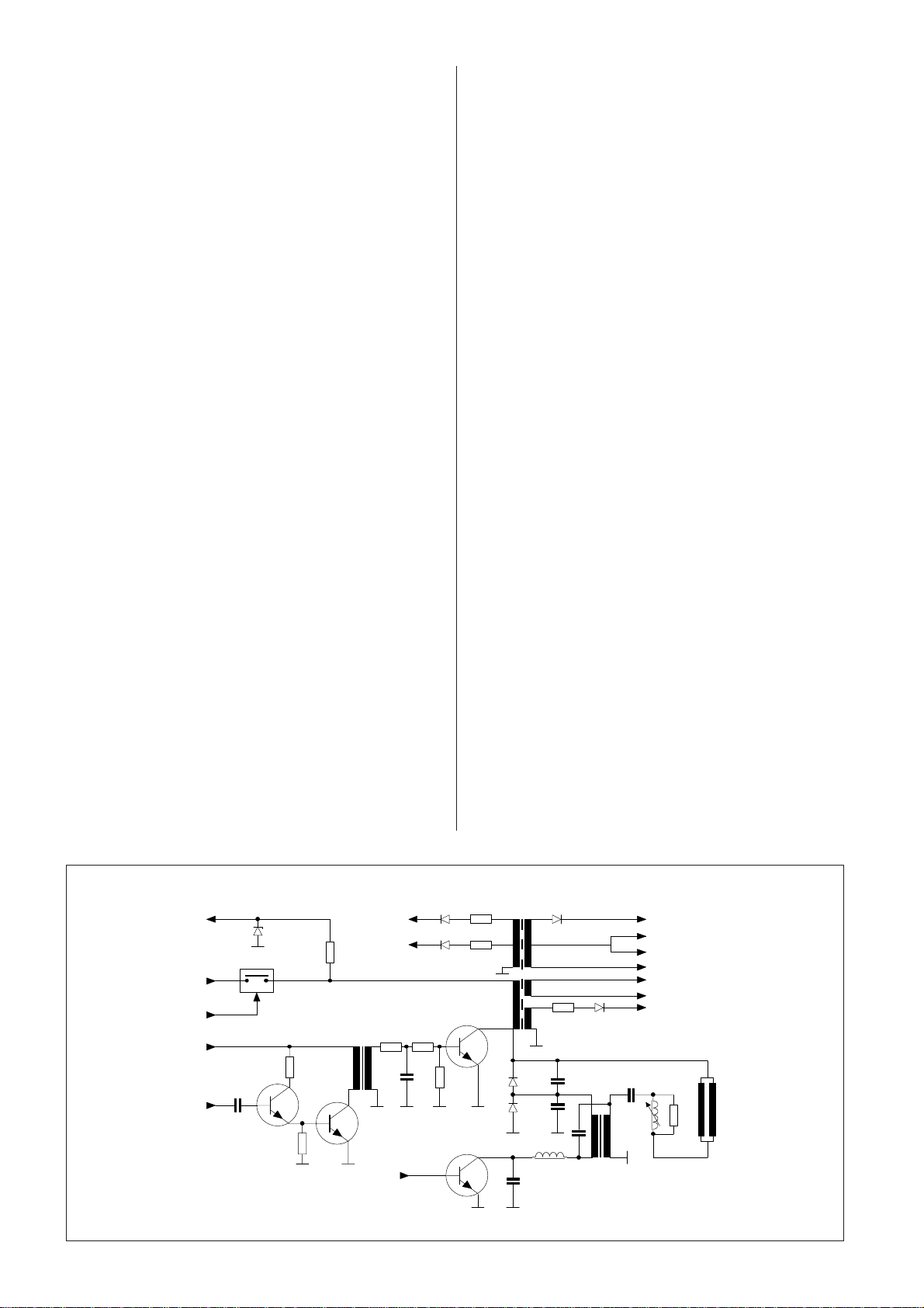
20
n
Korrekturschaltkreis steuert, der aus den Kondensatoren
Ck26, Ck28, der Diode Dk8 und dem Brückentransformator
Mk3 besteht.
Die Bildbreite und die Ost-West-Korrektureinstellungen
(Kissen, Bildecken undTrapez) werden durch Modulation
des Stroms über die Spule Lk1 durchgeführt.
Der Schaltkreis Ck38, Dk9, Rk49 und Rk52 parallel geschaltet
mit dem Kondensator Ck27 der S-Korrektur verhindert die
Erscheinung eines sogenannten„Mausezahns”.
Dynamischer Fokus, FO600
Eine dynamische Fokuseinstellung wird zusätzlich zur
normalen Fokuseinstellungverwendet. Der dynamische
Fokus verbessert den Fokus auf beiden Seiten
desBildschirms. Um eine höhere Fokusspannung am
Anfang und am Ende derAbtastperiode zu erhalten, wird
eine Hilfsspannung benötigt. Diese Spannung wird
einemTransformator abgenommen, der in Reihe mit der
Horizontalablenkspulegeschaltet ist. Die Kissenspannung
über den Transformator wird durch einenKondensator zum
Potentiometer für den dynamischen Fokus und weiter zu
einem diskreten Fokusgitter geleitet.Der dynamische Fokus
wird nur bei größeren Bildröhren verwendet.
Horizontale Zeilenlage und dynamischer Fokus,
FO7xx
Fernsehgeräte mit einem VGA-Anschluß (Feature-Box
DB700) sind mit einemspeziellen FO7xx-Modul
ausgestattet, das eine Einstellung der horizontalen
Zeilenlage und - falls erforderlich - des dynamischen Fokus
beinhaltet.
Die Steuerspannung für die Horizontallage (0...+5 V) wird
von Pin 5 desMicrocontrollers zum Modulanschluß Xfo3
geleitet. Der Anschluß Xfo3-2 ist an+12 Vp angeschlossen.
Wenn die Steuerspannung niedrig ist, leitet der Transistor
tfo5. Aufgrund der Widerstände rfo4, rfo5 und rfo6 ist die
Basisspannung an den Transistoren tfo3und tfo4 niedrig
und tfo3 und Tfo1 zum Leiten bringt. Die Diode Dfo2
leitetund der Kondensator Cfo7 wird auf die positive
Spannung aufgeladen, die weiter zur Ablenkstrecke über
den Widerstand Rfo2 und die Transformatorenpins 2 und
4geleitet wird.Wenn die Steuerspannung hoch ist, wird der
Transistor tfo5 abgeschaltet unddie Widerstände sind nicht
parallel mit rfo6 verbunden. Das bedeutet, daß
derSpannungspegel an den Basen von tfo3 und tfo4 hoch
ist und tfo4 sowie Tfo2 zumLeiten bringt. Die Diode Dfo1
leitet und der Kondensator Cfo6 wird auf die
negativeSpannung aufgeladen, die weiter zur
Ablenkstrecke geleitet wird. Durch Verändern der
Steuerspannung zwischen 0 und 5 V kann die
Ablenkstreckenegativer oder positiver eingestellt werden,
sodaß die Horizontalabtastungseitlich verschoben werden
kann. Die Kondensatoren Cfo2 und Cfo3 arbeiten als SKorrekturkondensatoren. Dasbedeutet, daß bei VGAFernsehgeräten die originalen S-Korrekturkondensatoren
(Ck27 und Ck 33) auf der Hauptplatine kurzgeschlossen
werden.
Der Kondensator Cfo4 und die Spulen Lfo1 und Lfo2
bewirken eine zusätzlicheKorrektur der Linearität.
Diodenspalttransformator Mk1
Die Primärwicklung (Pin 6) des Diodenspalttransformators
(DST) ist über denFET-Schaltkreis Tsw1 an eine
Versorgungsspannung von +130 V angeschlossen. Umden
Schalttransformator im Netzteil zu schützen, wird der
Energieverbrauch inder Ausschaltphase durch den FET
reduziert. Während des Normalbetriebes leitet der
FETaufgrund des hohen Pegels am Gatter.Wenn das
Fernsehgerät ausgeschaltet wird, fällt die +12 Vp und der
TransistorTsw2 leitet. Der Kondensator entlädt sich über
Transistor Tsw3, der dannleitet und das Gatter erdet und
somit den FET ausschaltet.
Der DST überträgt die Rückschlagimpulse von der
Primärwicklung (Pins 3 - 6) zuden Sekundärwicklungen und
erzeugt folgende Spannungen:
- Hochspannung (30kV) für die Bildröhrenanode
- Fokus und Schirmgitter (Ug2) für die Bildröhre
- Heizfadenspannungen für die Bildröhrenkathode von den
Pins 10 - 11
- +200 V für die Videoausgangsverstärker von den Pins 12
- 4. Diese Spannungwird durch die Diode Dk1
gleichgerichtet
- +50 V von den Pins 1 - 5 oder +46 V von den Pins 2 - 5 für
den Vertikal-IC. Diese Spannung wird durch die Diode Dk2
gleichgerichtet
- +16 V für den Vertikal-IC von den Pins 7 - 5. Diese
Spannung wird durch die Diode Dk3 gleichgerichtet
- EHT-Daten von Pin 8 (und Ck21)
+30 V
U1
+12 Vp
+17 V
Hor
drive
ZDk1
Tsw1
Tk1
Rk11-14
Tk2
Mk2
+53 V
+16 V
E-W
drive
Dk2
Rk9
Dk3 Rk19
Tk3
Tk4
Mk1
Dk7
Dk8
Ck26
Ck28
Lk1
Rk2 Dk1
Ck24
Mk3
Ck27/33
Lk2
EHT 30 kV
Focus
Ug2
EHT compensatio
Filament 6.3 V
+200 V
Defl
coil
Page 57

OPTIONEN
Aktive Subwoofer
Kammfilter CF700
SVM-Modul
Audio-Feature AR700
Audio-Feature AR701
Audio einstellbar TA700
Scart 3 + VGA-Audio TA710
Scart 3 TA711
Bild in Bild PP700 / 710
Aktive Subwoofer
21
Allgemein
Das Aktive Subwoofer-System erzielt eine klare
Verbesserung des Stereoklangs.Das System besteht aus
aktiven Filtern, Leistungsverstärkern, einem Subwooferund
Stereolautsprechern. Die Aktive-Subwooferstufe ist für die
Verwendungeiner internen Subwooferbox und
Stereolautsprechern im Fernsehgerät oder für kleine,
externe Frontlautsprecher konzipiert.
Funktionsbeschreibung
Die linken und rechten Stereokanäle werden bereits im
Soundprozessor MSP3410Dzusammengeführt. Der
Soundprozessor enthält auch die erforderlichen
Tiefpaßfilter für den Subwooferkanal und Hochpaßfilter für
die Lautsprecherkanäle.
Das Signal wird von Pin 31 des Soundprozessors
abgenommen und weiter zum Hochpaßfilter (40 Hz)
geführt, der aus dem Transistor ta6 und damitverbundenen
Bauteilen besteht.
Das gefilterte Signal wird dann zum AudioLeistungsverstärker ICa4 geführt.Der Verstärker kann
stummgeschaltet werden, indem Pin 1 auf LOW gebracht
wird.Das Steuersignal für die Stummschaltung wird vom
Microcontroller (Pin 51) überdie Transistoren ta10, ta4 und
ta5 abgenommen. Diese Stummschaltefunktion
schaltetjeden der Audio-Leistungsverstärker im
Fernsehgerät stumm. DerSubwoofer-Verstärker kann
jedoch auch separat stummgeschaltet werden;
diesesgeschieht über den Audioprozessor. Ein hoher Pegel
an Pin 5 steuert den Transistor ta5 leitend, der nurden
Subwoofer-Verstärker stummschaltet. Aufgrund des
Widerstandsnetzwerkesra106, ra105 und ra14 wird die
zentrale Stummschaltung in diesem Fall nichtaktiviert.
Der Verstärker arbeitet in einer Brückenkonfiguration. Die
Ausgänge sindintern zu den jeweiligen Eingängen jedes
anderen invers gegengekoppelt. Dieverstärkten, in der
Phase gegenläufigen Signale werden von den Pins 4 und
6zum Subwoofer-Lautsprecher geleitet.
Kammfiltermodul, CF700
Allgemein
Die Grundfunktion des Kammfilters ist die Trennung der
Luminanz- (Y) undChrominanzsignale (C) vom CVBS-Signal. Die Vorrichtung minimiert Probleme wiePunktflimmern
und Übersprechen (Cross Colour) während der Y / CTrennung.Zusätzlich dazu gibt sie dem EingangsVideosignal eine erweiterte Frequenzbandbreite.
Diesesgeschieht durch die Verwendung einer Taktfrequenz
in vierfacher Höhe derFarbhilfsträgerfrequenz. Der Filter
ist in der Lage, Signale nach PAL- undNTSC 3.58-Standard
zu verarbeiten. Das Modul enthält zwei IC’s: Den Multiplexer-Schaltkreisicc1 und den Kammfilterschaltkreis icc2.
Funktionsbeschreibung
Abhängig vom Standard umgeht oder filtert das Modul die
Eingangssignale wiefolgt:
PAL und NTSC 3.58
Das Signal wird zum Kammfilter-IC geleitet und in
Y- undC-Signale getrennt
NTSC 4.43 und SECAM
Das Signal wird zum Kammfilter-IC geleitet, jedoch
nichtgetrennt
S-VHS Das Signal wird zum Multiplexer-IC geleitet
Der Standard wird im Farbdecoder Icd1 identifiziert. Die
Information über denStandard wird über den IIC-Bus in den
Microcontroller und wieder zurück zumFarbdecoder
geleitet. Die Information wird von Pin 23 zu Pin 1 des
Kammfiltermoduls, von Pin 16 zu Modulpin 2 und von Pin
15 zu Modulpin 13 geleitet.
Der Modulpin 1 steuert den Multiplexer, das Videosignal
(„L”) entwedervorbeizuleiten oder das Signal zum
Kammfilter-IC („H”) zu leiten.Wenn Pin 1 HIGH ist, leitet er
die Farbhilfsträgerfrequenz (Fsc) zu eineminternen
Taktgenerator des Kammfilter-IC’s.Der Modulpin 2 legt die
Arbeitsweise des Kammfilters fest, entweder PAL („L”)oder
NTSC 3.58 („H”).
Der Modulpin 13 steuert den Kammfilter-IC dann im
Kammfilterbetrieb zu sein,wenn der IC die Y / C-Trennung
durchführt; oder im Umgehungsmodus („L”) zusein, wo
das Signal nicht getrennt, sondern nur über eine
interneVerzögerungsstufe geleitet wird. Zusätzlich
informiert der Pin 13 durch den Transistor tc3(BasisKollektorverbindung) den Farbdecoder über das
vorhandene Modul.Abhängig vom verwendeten Standard
sind die logischen Hoch- /Tiefpegelkombinationen wie folgt:
Standard Modulpin 1 Modulpin 2 Modulpin
13
PAL “H” + 4.43 “L” “H”
NTSC 3.58 “H” + 3.58 “H” “H”
NTSC 4.43 “H” + 4.43 “L” “L”
SECAM “H” + 4.28 “L” “L”
S-VHS “L” “L” “L”
Page 58
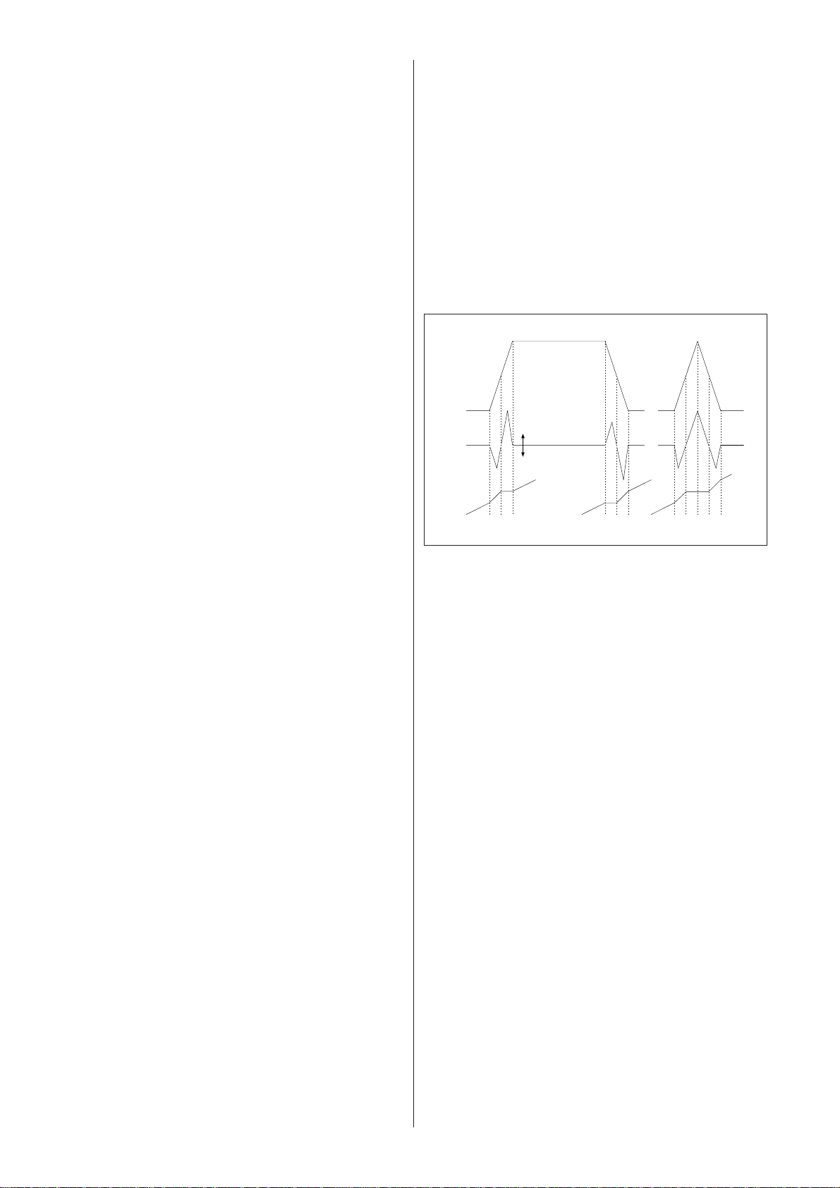
22
PAL-Signal
Das PAL-CVBS-Signal von Modulpin 6 wird an Pin 4 des
Multiplexers eingegeben.Wegen des hohen Pegels am
Steuerpin (siehe Inverter tc10) wird das Signal anPin 5
ausgegeben und weiter über eine Verstärkerstufe tc7 / tc8
zu einemTiefpaßfilter geleitet. Nach diesem Tiefpaßfilter
und dem Puffertransistor tc9 wird dasSignal an Pin 15 des
Kammfilter-IC’s eingegeben.
Im Kammfilter-IC wird das Videosignal an einen internen
Pegel geklemmt unddann durch einen
Hochgeschwindigkeits-8 bit A/D-Wandler gewandelt. Die
Wandlungsfrequenz beträgt das Vierfache der
Farbhilfsträgerfrequenz. Aufgrunddes PAL-Standards
beträgt die Farbhilfsträgerfrequenz an Pin 45 4,43 MHz,
daher beträgt diegewandelte Frequenz 17,7 MHz.
Ein logisches LOW an Pin 41 steuert die Eingabe der
Videodaten in dieKammfilter-Bearbeitungseinheit und ein
logisches LOW an Pin 47 legt die Filterweise in
Übereinstimmung mit dem PAL-Standard fest. Die
getrennten Luminanz- und Chrominanzdaten werden dann
durch zwei 8-bit D/A-Wandler in analoge Form gewandelt.
Die Wandlung wird unter Verwendung der gleichen
Taktfrequenz von 17,7 Mhz durchgeführt.
Das Luminanzsignal wird an Pin 6 ausgegeben, geht über
den Emitterfolger tc11 zu Pin 12 des Multiplexers und wird
an Pin 14 ausgegeben und dann durch den Emitterfolger
tc6 zum Ausgangspin 10 des Moduls weitergeführt.
Das Chrominanzsignal wird an Pin 8 ausgegeben, geht über
tc12 zu Pin 2 des Multiplexers und wird von Pin 15
ausgegeben und dann durch tc4 zum Ausgangspin11 des
Moduls weitergeführt.
NTSC 3.58-Signal
Die Signalwege sind exakt die gleichen wie die PALSignalwege. Der einzigeUnterschied besteht im
Kammfiltersystem im Kammfilter-IC. Pin 47 ist HIGH,daher
wird eine andere Filterweise gewählt. Die gewandelte
Frequenz beträgthierbei 14,3 MHz aufgrund der
Farbhilfsträgerfrequenz von 3,58 MHz an Pin 45.
NTSC 4.43- und SECAM-Signale
Der Signalweg zum Kammfilter-IC ist der gleiche wie oben.
Jedoch ist jetzt derPin 41 HIGH und daher ist der
Kammfilter-IC im Umgehungsmodus. Das Signal wirdnur
über den A/D-Wandler, die Speichereinheit und den D/AWandler geleitet.Die gewandelten Frequenzen betragen
17,7 MHz (NTSC) und 17,1 MHz (SECAM).Die NTSC 4.43und SECAM-Signale werden über den Kammfilter-IC
geleitet, weildie interne Speichereinheit eine zweizeilige
Verzögerung des Signals bewirkt.Wurden diese Signale
bereits im Multiplexer vorbeigeleitet und der
empfangeneStandard ändert sich, z.B. von SECAM zu PAL,
kann ein kurzzeitiger Verlust derSynchronisierung auftreten
Modulationsmodul für die
Abtastgeschwindigkeit, VM600
Allgemein
Der Zweck des Modulationsmoduls für die
Abtastgeschwindigkeit ist eine Steigerung der Bildschärfe
während der Intensitätstransienten des Luminanzsignals.
Die Modulation der Abtastgeschwindigkeit wird
durchgeführt, indem dasLuminanzsignal (a), das
Intensitätstransienten enthält, zuerst differenziertund dann
verstärkt wird.
Auf diese Art wird das so erzeugte Signal zu einer Hilfsspule
geleitet, diesich am Hals der Bildröhre befindet. Der Strom,
der während derIntensitätstransienten durch die SVMSpule fließt, moduliert das Ablenkfeld (c) und steigert oder
verlangsamt somit die Abtastgeschwindigkeit.
White
Luminance
signal
Black
SVM
signal
Deflection
Chess pattern
Scan velocity slower
Scan velocity faster
Basic principle of Scan Velocity Modulation
Das Luminanzsignal wird zuerst durch zwei
aufeinanderfolgendeDifferenzierglieder bestehend aus
cvm2/rvm2 und cvm1/rvm1/rvm3 abgezweigt.
Das abgezweigte Signal wird durch die Transistoren tvm1
und tvm2 vorverstärktund dann zur Begrenzerstufe geleitet,
die aus einem Differentialverstärker undden Transistoren
tvm3 und tvm4 besteht.
Das begrenzte Signal wird dann über eine Steuerstufe
(tvm6 und tvm7) zu denTransistoren Tvm8 und Tvm9, die
die Endstufe bilden, und weiter zur SVM-Spulegeleitet.
Grid pattern
a)
b)
c)
S-VHS-Signal
Das S-VHS-Signal wird an den Modulpins 6 (Y) und 7 (C)
und weiter an den Pins4 und 1 des Multiplexers
eingegeben. Der Pin 1 des Moduls ist jetzt LOW, wasein
HIGH des Steuerpins 9 verursacht; die internen Schalter
des Multiplexerswechseln in den Umgehungsmodus. Das
Luminanzsignal wird an Pin 14 und dasChrominanzsignal
wird an Pin 15 ausgegeben.
Handelt es sich bei derÜbertragung um ein reines
Monochromsignal oder reines Rauschen, was bedeutet,daß
kein Burst vorliegt, wird das Signal wie ein S-VHS-Signal
vorbeigeleitet. Dieses wird so durchgführt,weil kein
Farbhilfsträger vorhanden ist, der für die
Signalverarbeitungbenötigt wird.
Page 59
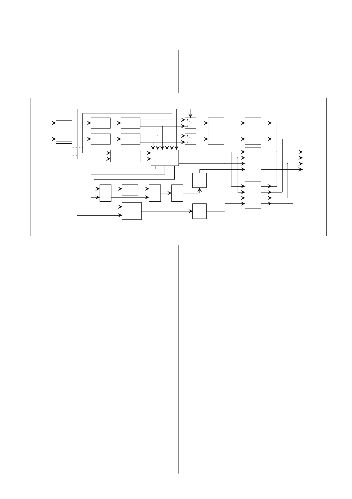
Audio Feature-Module, AR700 und
AR701
23
Allgemein
Das Audio Feature-Modul AR700 basiert auf einem
sogenannten 3D-Audiosystem,das die Audiosysteme 3D
Mono, 3D Stereo und 3D Movie-System abdeckt.
Das Audio Feature-Modul AR701 beinhaltet nicht nur die
oben erwähnten Systeme, sondern auch das Dolby Surround Pro Logic-System.
R
L
L
L
Input
Balance
R
Noise
Generator
Bass &
Treble
Bass &
Treble
Equ Control
_GLE_GE
L
R
_GLE_GE
Graphical
Equalizer
Graphical
Equalizer
L
Adaptive
R
Matrix
S_ Equ (from
S_ Orig (from L/R)
7kHz
LPF
GLE / GE
Dolby B
Level
Echoing
for 3D
Mono
GLE
L
GE
R
GLE
R
GE
Combining
Network
)
Dolby
B
Signal process in the DSP
Beide Systeme werden unter Anwendung digitaler
Tonverarbeitung erzeugt, derenProgramm aus sieben
Hauptblöcken besteht: Dolby Pro Logic, 3D Mono, 3D
Stereo,3D Movie, grafischer Equalizer, Klangregler und
Rauschgenerator.
Equ Control
L
3D
Stereo
L
R
C
3D
Movie
on/off
Delay
3D
Mono
on/off
Volume
ST
Stereo
Volume
DPL
Volume
ST Surround
R
L
R
C
S
L
R
C
S
L
R
C
S
Principle of the signal process in the DSP
Dolby Surround Pro Logic
Das Dolby Surround Pro Logic ist ein vierkanaliges Surround Sound-System.
In der Übertragungsphase ist die Vierkanalinformation in
zwei Kanäle (L’ undR’) codiert. Der mittlere (C) und die
Surroundkanäle (S) werden zu den linken(L) und rechten
(R) Kanälen nach der folgenden Formel hinzuaddiert:
- L’ = L + C x (-3 dB) + S x (-3 dB)
- R’ = R + C x (-3 dB) - S x (-3 dB)
Die Mittenkanalinformation wird zu den L- und R-Kanälen
in der gleichen Phasemit dem Faktor 0,7 addiert. Die
Surroundkanalinformation wird zu den L- und R-Kanälen
mit dem Faktor 0,7 addiert, jedoch in der gegenläufigen
Phase als +90° zum L-Kanal und als -90° zum R-Kanal.
Im Fernsehgerät entschlüsselt der Dolby Pro Logic-Decoder
die beiden Kanäle, L’ und R’, wieder in vier getrennte
Kanäle, links, mittig, rechts undSurround. Falls die
Übertragung Dolby Pro Logic-Ton enthält, schaltet
dieSoftware das Fernsehgerät automatisch in den Pro
Logic-Modus, vorausgesetzt das Fernsehgeätbefindet sich
im AUTO-Betriebsmodus, die Übertragung ist in Stereo
(Nicam oderA2) und die WSS- (Wide Screen Signalling)
Daten beinhalten das Dolby-Bit. Zusätzlich müssen die
rückseitigen Lautsprecher angeschlossen sein, da sonst die
Software den 3D Movie-Betriebsmodus wählt.
Während der digitalen Signalverarbeitung werden die
Audiodaten (L’ und R’) zuerst zur EingangsBalancesteuerung geleitet, die mögliche Fehler des
Pegelszwischen den beiden Eingangssignalen kompensiert.
Die Balancesteuerung ist fürautomatischen Betrieb
konzipiert und somit sehr benutzerfreundlich. Das
automatischeSystem überprüft fortwährend den
Pegelunterschied zwischen den linken undrechten Kanälen
und versucht, diesen so klein wie möglich zu halten.
Als nächstes wird das Signal zur adaptiven Matrixstufe
geleitet, deren ersteEinheit ein Bandpaßfilter ist. Die
Hochpaßfrequenz dieses Filters beträgt 200Hz und die
Tiefpaßfrequenz beträgt 5 kHz. Nach den Bandpaßfiltern
werden die Daten (Lbp und Rbp) zu einer Berechnungs
einheit geleitet, die den mittleren Kanal unddie
Surroundkanäle erzeugt. Die Berechnungsformel lautet Cbp
= Lbp + Rbp and Sbp = Lbp - Rbp.
Die absoluten Werte werden dann von den Lbp-, Rbp-, Cbpund Sbp-Signalenabgenommen. Der nächste Schritt ist die
Berechnung des Verhältnisses zwischendem linken und
rechten Kanal sowie zwischen dem mittleren und dem
Surroundkanal.
Anschließend erfolgt die Berechnung der Zeitkonstante. Im
Dolby Pro Logic-Decoder gibtes zwei Zeitkonstantenfilter.
Der Pegel des Signals bestimmt, welcher davongewählt
wird. Falls der Unterschied des Pegels zwischen linkem und
rechtemKanal oder zwischen dem mittleren und dem
Surroundkanal mehr als 5,5 dB beträgt, wirdeine Filterung
der Langzeitkonstanten durchgeführt. Danach wird der Filter fürdie Kuzzeitkonstante berechnet. Falls der Unterschied
des Pegels weniger als5,5 dB in beiden Richtungen beträgt,
wird nur die Filterung der Kuzzeitkonstante durchgeführt.
Schließlich werden die LR- (links/rechts) und CS-(mittig/
Surround) Signaledurch eine Polaritätsbestimmungseinheit - der letzten Bearbeitungseinheit inder adaptiven
Matrixstufe - zu der kombinierenden Netzwerkstufe geführt.
Nach der kombinierenden Netzwerkstufe wird nur die
Bearbeitung desSurroundkanals fortgeführt. Im
Surroundkanal befindet sich ein 7kHz-Tiefpaßfilter, eine
Verzögerung sowie ein modifizierter Dolby-B-Decoder.Der
Tiefpaßfilter ist einfach ein Filter zweiter Ordnung, dessen
Abschaltfrequenz 7 kHz beträgt. DieVerzögerung kann eine
variable Verzögerung von 15 ms bis 30 ms oder
einekonstante Verzögerung von 20 ms sein.Der modifizierte
Dolby-B-Decoder ist ein komplexer Teil der Bearbeitung.
DieVerstärkung des Dolby-B-Filters ist von der Frequenz
des Eingangssignales undauch vom Pegel des
Eingangssignales abhängig. Das Programm verwendet
Page 60
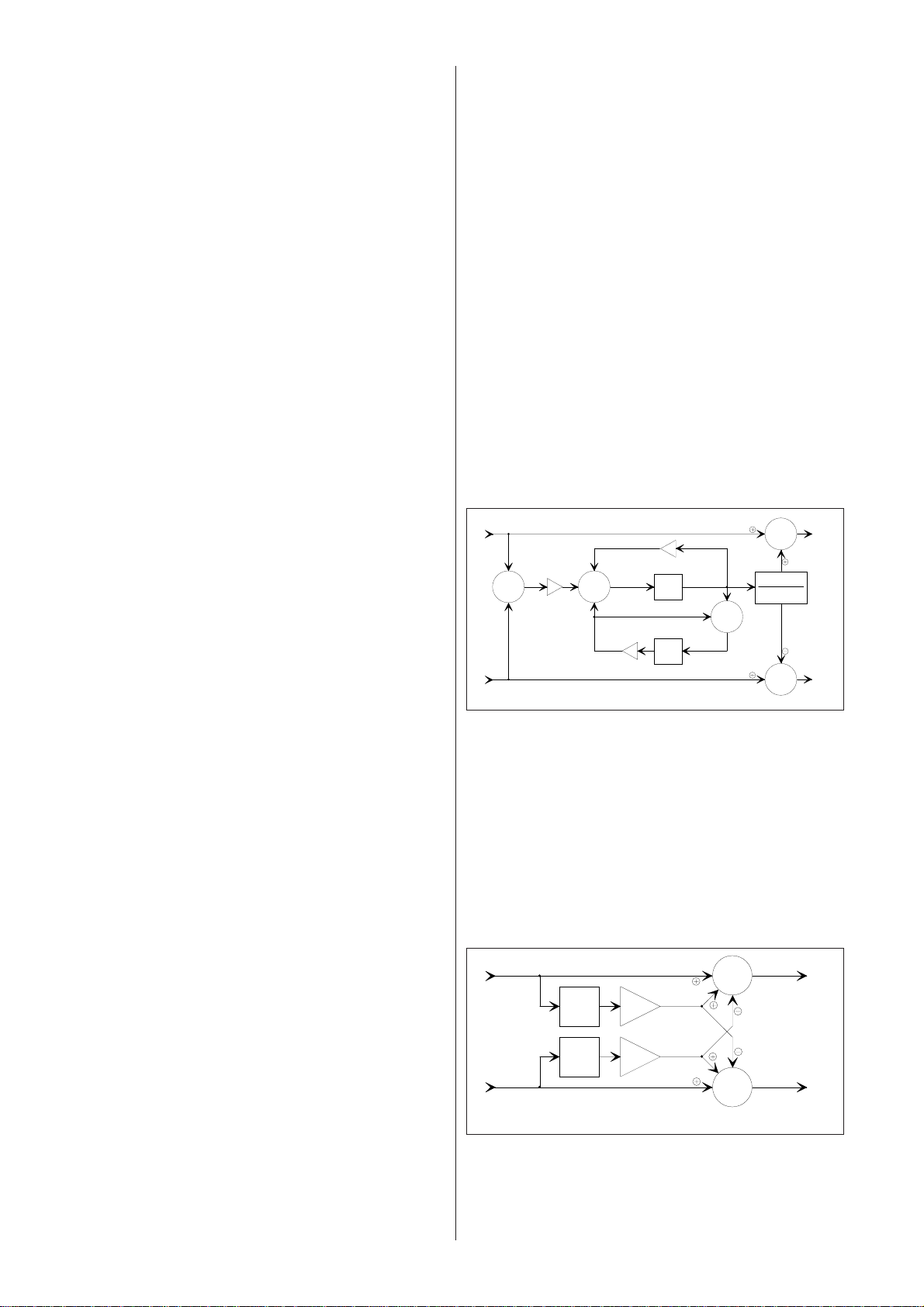
24
p
einSurroundkanalsignal, das ohne Grafik- (GE) und
Lautsprecherausgleich (GLE) für denDolby-B-Pegel sowie
Frequenzberechnungen ausgelegt wird.Der Dolby-BFiltervorgang wird am entzerrten Signal durchgeführt.
Im Dolby Pro Logic-Decoder gibt es drei verschiedene
Kanalbetriebsarten: Weit,Normal und Phantom.
Weit-Modus
Wenn alle drei Frontlautsprecher tiefe Bassfrequenzen
wiedergeben können undgenügend Verstärkungsleistung
aufweisen, kann sich das System im Weit-Modusbefinden.
Weit ist eine Abkürzung von Weitband, was bedeutet, daß
das gesamteFrequenzband vom mittleren Lautsprecher
wiedergegeben wird.
Normal-Modus
Falls zwei Full range-Lautsprecher für den linken und
rechten Kanal vorhandensind, ist die einfachste Weise, das
Dolby Pro Logic-System aufzubauen, dasHinzufügen eines
Lautsprechers für den mittleren Kanal irgendwo in der
Nähedes Bildschirms. Die kleinen Lautsprecher sind
normalerweise nicht in der Lage, tiefeBasswerte
wiederzugeben. Im Normal-Modus ist das Ansprechen des
mittlerenKanals auf 100 Hz begrenzt und der Baßgehalt wird
auf den linken und rechtenKanal (oder alternativ zum
Subwoofer) umgeleitet. Eine andere Bezeichnung für
diesen Modus ist„Baßspaltmodus”.
Phantom-Modus
Falls kein mittlerer Lautsprecher vorhanden ist, kann der
Decoder auf denPhantom-Modus eingestellt werden. In
diesem Modus werden alle Daten für denmittleren Kanal
den linken und rechten Lautsprechern hinzugefügt.
Für den Surround-Kanal gibt es zwei Betriebsarten: Normal und 3 Stereo.
Im 3 Stereo-Modus ist der Surround-Ausgang nicht
verfügbar. Die Surround-Datenwerden ignoriert und den
anderen Kanälen nicht hinzugefügt.
Zusammenfassend gibt es im Prinzip vier verschiedene
Lautsprecherkonfigurationen.
Signal (oder aus der Summe der linken und rechten Kanäle)
nach dengrafischen Equalizern erzeugt. Diese Betriebsart
ist für Programme ohne Dolby Pro Logic geeignet,bei denen
ein Surround-Kanal gewünscht wird. Der 3D Mono-Modus
erfordert keine externen Lautsprecher.
Der künstliche Surround-Effekt wird aus dem Monosignal
erzeugt. Der Effektbesteht hauptsächlich aus einem Echo,
wobei die Größe des Raumes künstlichdurch die
Verzögerungssteuerung und die Fülle durch die
Effektsteuerungverändert werden kann.
Das 3D Mono-System wird auch 3D Pseudo- oder SemiTech Surround-System genannt.
Das Signal wird an den graphischen Equalizern
abgenommen und zur Dämpfungseinheit geleitet, um einen
Überlauf zu vermeiden. Die Koeffizientenstufe 1 und der
Verzögerungspuffer 2 weisen konstante Werte auf.Der
Multplikationsfaktor beträgt 0,12 und die Verzögerungszeit
ist aufgrund der Größe des Verzögerungsspeichersauf 104
ms begrenzt. Der Regelbereich für den Verzögerungspuffer
1 liegtzwischen 50 ms und 150 ms und der
Multplikationsfaktor der Koeffizientenstufe2 liegt zwischen
0,1 und 0,2. Im Tonmenü werden diese Einstellungen Effekt
und Verzögerunggenannt.
Schließlich wird das multiplizierte und verzögerte Signal
zum HRTF-Filtergeleitet, der den Lautsprecherklang
künstlich von seinem wirklichen Platz aneine andere Stelle
versetzt.
L
coef 1
++
-18dB
R
Principle of the 3D Mono system
-1
Z
delay 1
-1
Z
delay 2coef 2
1
H + H
Left
+
i
c
++Right
Volle Konfiguration (5 Lautsprecher)
- aufgeteilt in zwei externeFrontlautsprecher (L / R),
mittlerer Lautsprecher und zwei externe rückseitige
Lautsprecher
Phantom-Modus (4 Lautsprecher)
- die eigenen Lautsprecher des Fernsehgerätes(L / R)
dienen als Frontlautsprecher, kein mittlerer
Lautsprecher und zweiexterne rückseitige Lautsprecher
3 Stereo (3 Lautsprecher)
- mit zwei externen Frontlautsprechern (L / R)und
mittlerem Lautsprecher, jedoch ohne rückseitige
Lautsprecher
Basiskonfiguration
- hierbei werden nur die eigenen Lautsprecher des
Fernsehgerätes (L / R) verwendet.
Bei Konfigurationen, in denen der mittlere Lautsprecher
verwendet wird, könnendieses entweder ein externer
Lautsprecher oder die eigenen Lautsprecher des
Fernsehgerätes - in Serie geschaltet - sein. Ein Subwoofer
kann zusätzlich zuden oben erwähnten Lautsprechern
verwendet werden.
Das Dolby Surround Pro Logic-System besteht aus dem
Taktgeber icar1, aus demdigitalen Soundprozessor icar2,
dem Verzögerungsspeicher icar3, derphasengekoppelten
Schleife icar4, der Rekonstruktionsfilterung /Digital-/
Analogwandlung icar5 und icar6, dem Leistungsverstärker
Icar7 und dem Lautsprecherwahlschalter SWA1.
3D Stereo
3D Stereo ist ein künstliches System, das zur Erweiterung
desStereoklangbildes der Lautsprecher im Fernsehgerät
dient und demnach keineexternen Lautsprecher erfordert.
Der 3D Stereomodus verstärkt nur dieStereowerte (ohne
Echo und Verzögerung), hat also keinen Einfluß auf eine
Übertragung, die nicht im Stereotonist. Die EffektSteuerung im Tonmenü verändert den Umfang der
Verstärkung fürdie Stereowerte.
Die Rate basiert auf einem Bandunterdrückungsfilter (BRF).
Der Ausgang diesesFilters wird mit einem veränderbaren
Koeffizienten multipliziert. Dieses Signal wird dann dem
ursprünglichen Kanal hinzugefügt und von demanderen
Kanal abgezogen.
L
BRF
Adj
+
Left
coef
BRF
Adj
coef
R
Princi
le of the 3D Stereo system
+
Right
3D Mono
Das 3D Mono-System ist für Monoübertragungen
konzipiert. Es handelt sich umein künstliches SurroundTonsystem, welches das Surround-Signal aus demMono-
Page 61
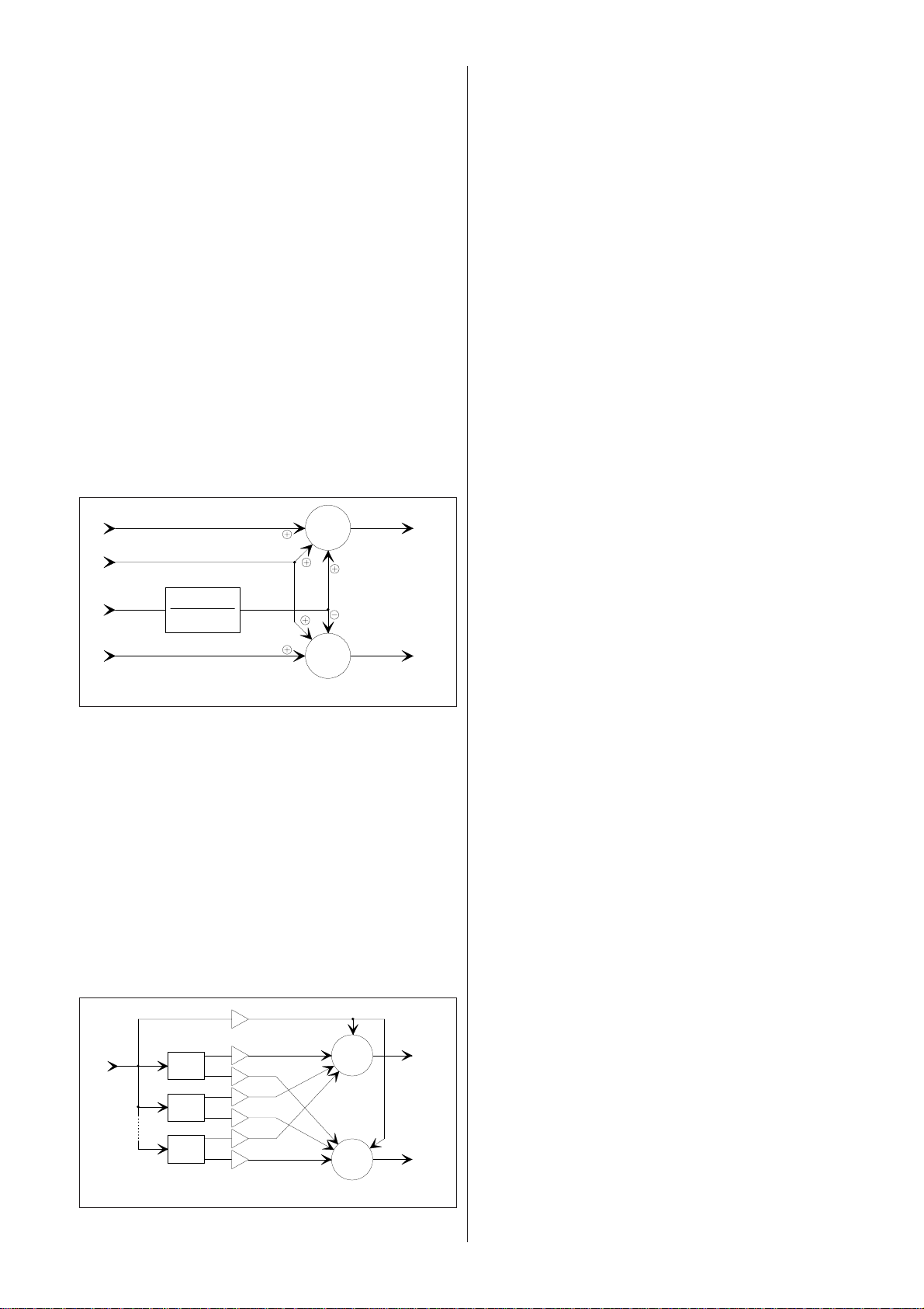
3D Movie
3D Movie ist eine bestimmte Art eines virtuellen SurroundTonsystems. Mitdiesem System können mehrere
Lautsprecher virtuell erzeugt werden, ohne diese
Lautsprecher wirklich zu installieren. Daher sind nur die
eigenen Lautsprecherdes Fernsehgerätes erforderlich, um
ein Klangerlebnis wie in einem Kino zu schaffen. Der
dreidimensionale Effekt wird künstlich durch die
Veränderung des Frequenzgangserzeugt, so daß der Ton
scheinbar aus einer anderen Richtung als aus derRichtung
des eigentlichen Lautsprechers kommt.
Die Filter in dem System basieren auf der HRTF-Technik.
3D Movie erforderteine Dolby Pro Logic-verschlüsselte
Übertragung, um richtig funktionieren zukönnen, weil das
System zusätzlich zu den linken und rechten Kanälen
denmittleren Kanal und die Surround-Kanäle verwendet.
3D Movie arbeitet nur im Phantom-Modus. Dasbedeutet,
daß der mittlere Kanal den linken und rechten Kanälen
hinzugefügtwird. Die Effekt-Steuerung im Tonmenü
entspricht der Pegeleinstellung desSurround-Kanals im
Dolby Pro Logic-System.
Wenn die Übertragung Dolby Pro Logic-verschlüsselten Ton
enthält und sich das Fernsehgerät im AUTO-Modus
befindet, schaltet die Software das Fernsehgerät
automatisch in den 3D Movie-Modus, vorausgesetzt die
Übertragung ist in Stereo (Nicam oder A2) und die WSSDaten enthalten das erforderliche Dolby-bit.
25
Toneinstellung
Die Toneinstellungen, Baß und Höhen, sind nicht einzeln
als Baß- undHöheneinstellung einstellbar, sondern sie
dienen als Lautstärkeregelung. Dasbedeutet, daß die
Toneinstellung von der Lautstärkeregelung abhängig ist.
Rauschgenerator
Der Rauschgenerator wird zur gleichen Einstellung der
Kanalpegel verwendet.Normalerweise benötigt der
Benutzer dieses Programm nur während der Plazierungder
Lautsprecher. Der Rauschgenerator leitet den Rauschwert
an jedenangeschlossenen Lautsprecherkanal. Dieses ist
hilfreich bei der Einstellung der relativenBalance zwischen
den separaten linken, rechten, mittleren und rückseitigen
Pegeleinstellungen in Bezug auf die Hörgewohnheiten.
L
+
Left
C
S
R
1
H + H
i
c
+
Right
Principle of the 3D Movie system
Grafischer Equalizer
Im digitalen Soundprozessor ist ein grafischer Equalizer
(7-Band) fürBedienereinstellungen sowie eine Korrektur für
den Frequenzgang derLautsprecher. Jedes der sieben
Bänder (es wurden nur drei im Schaubild untengezeichnet)
hat zwei Ausgänge.Die Kanäle, die einen Ausgleich für den
Frequenzgang der Lautsprecheraufweisen, haben einen
Lautsprecherausgleich und eine benutzerdefinierte
Verstärkung (gGLE). Die Kanäle ohne Lautsprecher
ausgleich haben nur einebenutzerdefinierte Verstärkung
(gGLE). Im Tonmenü gibt es vier verschiedene
voreingestellte Auswahl möglichkeiten: Musik, Sprache,
Flat und Normal. Im Musik-, Sprach- und Flat-Modus
übernimmt der Equalizer die Voreinstellungen von der NV
RAM. Im Flat-Modus sind die Equalizer-Einstellungen in der
mittleren Position fixiert. Nur im Normal-Moduskann der
Benutzer die Einstellungen verändern.
Xin
dir
g
GLE
H (z)
H (z)
H (z)
g
GE
g
GLE
g
GE
g
GLE
g
GE
g
Principle of the Graphical Equalizer
X
+
+
GLE
X
GE
Page 62
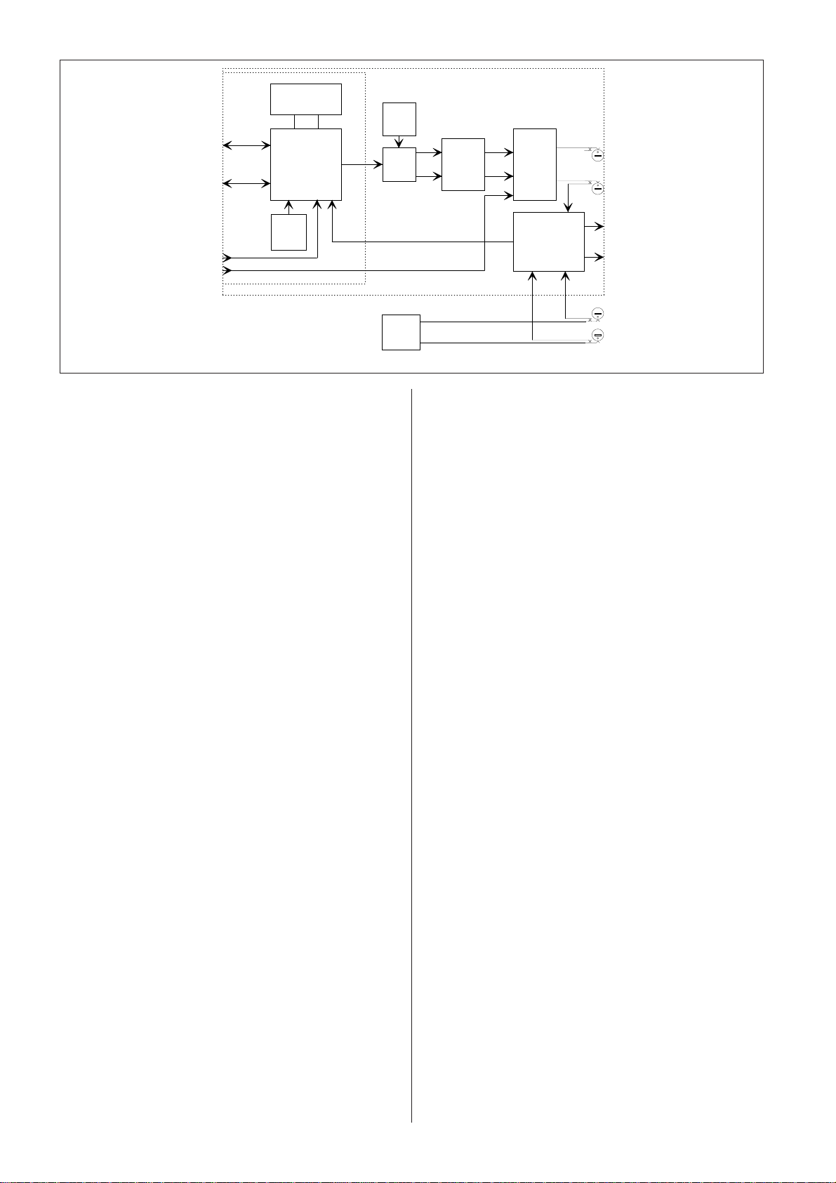
26
Delay memory
icar3
Signal
processor
icar2
Master
clock
icar1
PLL
icar4
DAC
icar5
Power
amplifier
ICa1
IIS-bus
Audio data
IIC-bus
Control
Reset
Mute
AR700
Block diagramme of the 3-audio (AR700) and 3D + Dolby Pro Logic module (AR701)
Funktionsbeschreibungen der Schaltkreise
Das Audio Feature-Modul AR700 besteht nur aus einem
Taktoszillator, einemSoundprozessor sowie einem
Verzögerungsspeicher.
Das Audio Feature-Modul AR701 besteht zusätzlich aus
einer phasengekoppelten Schleife, einem
Rekonstruktionsfilter, einem D/A-Wandler sowie einem
Leistungsverstärker.
AR701
Reconstruction
filter
icar6
Equalizer control
R
L
Power
amplifier
ICar7
L&R / center
speaker switch
SWA1
LR
To surround
speakers
To external
center speaker
To internal
speakers
To external
L/R speakers
Phasengekoppelte Schleife (PLL), icar4
Der Schaltkreis der phasengekoppelte Schleife erzeugt das
Haupttaktsignal für den D/A-Wandler. Die Schleife ist an
das IIS-WS-Signal (Pin1) gekoppelt, dasals 32 kHz
Systemtakt dient. Die phasengekoppelte Schleife
multipliziert das 32 kHz-Signal mit 384, was einem
endgültigen Haupttaktsignal von 12.288 MHz entsprichtund
an Pin 10 ausgegeben wird.
Taktoszillator icar1
Der Inverter-Schaltkreis icar1 arbeitet als Haupttakt
oszillator, dessen Frequenz von 25 MHz durch den
Widerstand rar1 und den Kondensator car1 bestimmt
werden. Die Taktimpulse werden von Pin 8 zu Pin 14 des
Soundprozessors geleitet.
Soundprozessor icar2
Der digitale Soundprozessor (DSP) enthält mehrere
verschiedene Speicher, undzwar ein 512 x 32-bit ProgrammRAM, ein 256 x 24-bit Daten-RAM, ein 256 x24-bit
Koeffizienten-RAM, 1,5 Kilo Word x 32-bit Programm-ROM
und ein 1,5 KiloWord x 32-bit Koeffizienten -ROM. Zusätzlich
enthält er eine 24-bit arithmetischeLogikeinheit (ALU) und
ein 25-bit x 25-bit Multiplizierakkumulator (MAC).Außerdem
enthält der Schaltkreis einen grafischen Equalizer, eine
Toneinstellung und einen Rauschgenerator.
Der Schaltkreis wird über den IIC-Bus gesteuert. Die Software zurSteuerung ist im Programmspeicher (ICf1)
gespeichert, von wo sie zumMicrocontroller (icf3) und
weiter über den IIC-Bus zum Soundprozessor geführtwird.
Alle Voreinstellungen sind im NV RAM (ICf2) gespeichert.
Um die ordentliche Funktion desIIC-Bus während des Einund Ausschaltens zu gewährleisten, werden sowohl
dieseriellen Daten (SDA) als auch der serielle Takt über die
von +12 Vgesteuerten FET’s tar1 und tar2 zum
Soundprozessor geleitet.
Der digitale Soundprozessor wird an den MSP (ICa2) über
den IIS-Busangeschlossen, der aus vier Leitungen besteht,
Dateneingang (IIS-DI),Datenausgang (IIS-DO), Wortwahl
(IIS-WS) und Takt (IIS-CLK). Das Signal fürdie Wortwahl ist
ein 32 kHz Rechteckimpuls und wird für die Trennung der
Kanäle verwendet. Das Taktsignalist ein 1,024 MHz
Sinuswellenimpuls und wird als Systemtakt verwendet.
Verzögerungsspeicher icar3
Der Verzögerungsspeicher ist ein 256 kbit (32k x 8) SRAM,
der zusammen mit demdigitalen Soundprozessor zur
Erzeugung der bei Dolby Pro Logic-, 3D Mono- und3D
Movie-Systemen benötigten Echoeffekte verwendet wird.
Rekonstruktionsfilterung und D/A-Wandlung, icar5
und icar6
Die Rekonstruktionsfilterung und D/A-Wandlung wird unter
Verwendung von zwei Schaltkreisen, dem D/A-Wandler mit
einem digitalen Filter, icar5 (TC9270) unddem
Filterschaltkreis, icar6 (TA2009F) durch geführt.Der TC9270
schließt eine serielle Eingangsschnittstelle, eine De-Emphasis, Interpolatoren, Delta-Sigma-Modulatoren und D/AWandler ein. Die Audiodaten werden an dem Pin 25
eingegeben und an den Pins 9 / 10 (Surround) sowie 5 / 6
(mittig) ausgegeben. Der gesamte Vorgang wird durchdrei
Taktsignale gesteuert, dem 1,024 MHz Systemtakt an Pin
2, dem 32 kHz Wortwahlsignal an Pin 3 und dem Haupttakt
an Pin 4. Analoge Audiosignale werden dann zu dem
Tiefpaßfilter schaltkreis TAA2009 geleitet, der die
Nachfilterung durchführt. Der Surround-Kanal wird von Pin
6 und der mittlere Kanal von Pin 3 zum Leistungsverstärker
geführt.
Leistungsverstärker Icar7
Der verwendete Leistungsverstärker TDA2616 ist der
gleiche wie er imAudioverstärker auf der Hauptplatine
verwendet wird. Er ist daher schon imAudioabschnitt
beschrieben worden.Der Surround-Kanal wird von Pin 4
zum Lautsprecheranschluß Qar6 geleitet. DieImpedanz der
Surround-Lautsprecher beträgt 16 Ohm, daher sind sie
parallelgeschaltet.
Der mittlere Kanal wird von Pin 6 zum
Lautsprecheranschluß Qar5 und zum Schalter SWA1
geleitet.
Lautsprecherwahlschalter SWA1
Er ermöglicht die Verwendung der internen Lautsprecher
des Fernsehgerätes alsLautsprecher für den mittleren
Kanal. Die internen Lautsprecher sind amAnschluß Q4
angeschlossen und daher geht der Signalweg vom
mittlerenKanalverstärker über die Pins 15 / 14 von SWA1,
Anschlußpin 1 (+), Lautsprecher, Anschlußpin 2 (),Anschlußpins 5 / 4 / 18 / 17, Anschlußpin 3 (+),
Lautsprecher, Anschlußpin 4(-), Schaltpins 2 / 1 sowie
Masse. Daher sind die internen Lautsprecher inReihe
geschaltet. Die Schaltpins 1 / 2 steuern den Soundprozessor
über den Pin 27 zurWahl des richtigen Ausgleichs. Bei
Page 63

dieser Lautsprecherkonfiguration müssen dielinken und
rechten Kanäle über die Lautsprecheranschlüsse Xexts1
und Xexts2auf der Hauptplatine an externe Lautsprecher
angeschlossen werden.
Wenn ein externer Lautsprecher für den mittleren Kanal
angeschlossen ist, istdie Verbindung zum Schalter
unterbrochen. In diesem Fall fordert die Softwareden
Benutzer auf, die Schaltposition zu ändern.
Die linken und rechten Kanäle von der Hauptplatine sind
am Anschluß Q3angeschlossen und aufgrund der anderen
Schaltposition werden die linken undrechten Kanalsignale
jetzt direkt über die Schalter zu den internenLautsprechern
geleitet. Voraussetzung ist natürlich, daß externe linke und
rechte Lautsprecher nichtangeschlossen sind.
Einstellbares Audioausgangsmodul
TA700
Das einstellbare Audioausgangsmodul (Leitungsausgang)
TA700 ermöglicht es, denTon des Fernsehgerätes unter
Verwendung von Klang- und Lautstärkeeinstellungender
vorhandenen Fernbedienung des Fernsehgerätes zu einem
externen Verstärkerzu leiten.
Die Audiosignale für den linken und rechten Kanal werden
über ein FET-Paar,tta1 und tta2, zum Operationsverstärker
icta1 geleitet. Aufgrund der negativenEingabe invertiert der
Verstärker die Signale. Verstärkte Signale werden dannüber
ein anderes FET-Paar, tta8 und tta9, zu den Ausgangs
anschlüssen Xt7 und Xt8 (RCA-Anschlüsse) geführt.
Diese FET-Paare vermeiden mögliche unerwünschte
Schaltspitzen vom Audioprozessor bei Erreichen des
externen Audioverstärkers.
Das erste Paar tta1 und tta 2 eliminiert mögliche positive
Störungsspitzen (interne Dioden) und aufgrund der
Invertiereigenschaft des Operationsverstärkers vermeidet
das zweite Paar tta8 und tta9 negative Spitzen, die vom
Audioprozessor kommen.
Ein- und Ausschalten der Dämpfung
Die FET’s dienen auch als Stummschaltekomponenten
(Dämpfung) während des Ein-und Ausschaltens.
Wenn das Fernsehgerät eingeschaltet wird, verursacht die
+12 Vp (über denTransistor tta5) den positiven Eingang an
Pin 5 von icta2 schneller in denHochpegelzustand zu gehen
als der negative Eingang an Pin 6. Das bedeutet, daßder
Ausgangspin 7 HIGH ist und die Transistoren tta6 und tta7
leiten und die Gates derFET’s auf LOW halten. Nach einer
kurzen Zeit, wenn der Kondensator Cta17aufgeladen ist,
leitet tta5 nicht mehr und die Spannung an Pin 5 fällt
unterden Wert von der Spannung an Pin 6. Der
Ausgangspin 7 ist jetzt LOW und die Transistoren tta6und
tta7 leiten nicht.Das erste FET-Paar bezieht die GateSpannung über den Widerstand rta24. Daszweite FET-Paar
weist eine leichte Verzögerung auf, da die Gate-Spannung
überden Transistor tta4, den Widerstand rta20 und den
Kondensator Cta15 bezieht.
Wenn das Fernsehgerät ausgeschaltet wird, geht der Pin 6
des icta2 sofort aufLOW, jedoch bleibt der Pin 5 aufgrund
der Ladung des Kondensators Cta18 aufHIGH. Der
Ausgangspin 7 ist demnach auf HIGH und die FET-Paare
werdenabgeschaltet.
Status am Leitungsausgang
Die andere Hälfte des Operationsverstärkers arbeitet als
Schalter für denStatus am Leitungsausgang. Wenn die
Ausgangsanschlüsse nicht benutzt werden,halten die
zusätzlichen Kontakte (an den Anschlüssen) den
negativenEingangspin 2 über die Widerstände rta17 und
rta18 auf LOW. Das bedeutet, daß der Ausgangspin 1 HIGH
ist, der Transistor ta9 (auf der Hauptplatine) leitet und hält
den Pin 3 desMicrocontrollers auf LOW (inaktiv).
Wird ein Stecker am Anschluß angeschlossen, trennt der
zusätzliche Kontakt denWiderstand rta17 / rta18 von der
Masse. Dieses verursacht einen höherenSpannungspegel
27
an Pin 2 und der Ausgangspin 1 geht auf LOW. Jetzt leitet
derTransistor ta9 nicht mehr und der Pin 3 des
Microcontrollers ist HIGH. Dieses ermöglichtdie Wahl von
drei verschiedenen Formen der Stummschaltung:
- Der Leitungsausgang ist in Betrieb, aber die Lautsprecher
des Fernsehgerätessind stummgeschaltet,
- Beide Leitungs ausgänge und die Lautsprecher des
Fernsehgerätes sindstummgeschaltet,
- Beide Leitungsausgänge und die Lautsprecher des
Fernsehgerätes sind inBetrieb (keine Stummschaltung).
Scart 3 + VGA-Audio-Modul TA710
Das Scart 3 + VGA-Audio-Modul TA710 ermöglicht, nicht
nur einen zusätzlichenScartanschluß, sondern auch einen
zusätzlichen Audioanschluß (VGA-Audio) zuhaben. Der
Audioeingang geht über die VGA-Audioanschlüsse, wenn
der VGA-Betrieb gewählt worden ist.
Die Eigenschaften von Scart3 sind mit denen von Scart 1
identisch.
Der RGB-Schalter ica2 wählt die Signale entweder von Scart
3 oder von Scart 1.Die RGB-Signale werden von Scart 1
über den Anschluß Xa5 geführt, der amAnschluß Xq7 auf
der Hauptplatine angeschlossen ist.Der Audioschalter ICa3
wählt die Signale entweder von Scart 3, „VGA” oder
vomKameranschluß. Der Anschluß Xa2 ist mit dem
Anschluß XA4 (auf derBedieneinheit am Fernsehgerät) und
der Anschluß Xa3 ist mit dem Anschluß Xtta (auf der
Hauptplatine) gekoppelt.
Der Spannungspegel an Modulpin 3 bestimmt, von
welchen Anschlüssen die RGB-und Audiosignale
abgenommen werden. Die Steuerspannung wird
vomVideotext-Schaltkreis (Pin 7, GPO) und weiter über die
Anschlüsse Xq5-3 (aufder Hauptplatine) und Xa1-3 (auf
dem Modul) abgenommen. Der RGB-Schalter ica2 wird
über den Pin 5gesteuert und der Audioschalter mit den
Spannungspegeln an den Pins 9 (=B) und10 (=A) gesteuert.
Das logische LOW liegt bei etwa < 3,5 V und das
logischeHIGH bei etwa > 9 V bei einer
Versorgungsspannung von +12 V. Der GPO (General Purpose Output) kann in drei Betriebszuständen sein:
HIGH,OPEN und LOW.
Wenn der GPO auf HIGH ist, leitet der Transistor ta2 und
zieht B auf LOW, dieDiode da2 und der Transistor ta4 leiten;
daher sind A und der Pin 5 von ica2auf LOW. Als Ergebnis
dieser Kombination werden sowohl die RGB- als auch
dieAudiosignale von Scart 3 abgenommen. Wenn der GPO
auf OPEN ist, leitet ta2 nicht und Bist auf HIGH, da2 und
ta4 leiten; daher sind A und der Pin 5 von ica2 auf LOW.Die
RGB-Signale werden von Scart 3 abgenommen, jedoch
werden die Audiosignalevom „VGA”-Anschluß
abgenommen.Wenn der GPO auf LOW ist, leitet ta2 nicht
und B ist auf HIGH. Die Diode da1leitet und zieht die Anode von da2 auf LOW. Diode da2 sowie der Transistor
ta4leiten nicht, und A und der Pin 5 gehen auf HIGH. Jetzt
werden die RGB-Signalevon Scart 1 (über Xa5) und die
Audiosignale vom Kameraanschluß (über Xa2)
abgenommen.
GPO B A RGB-Eingang Audioeingang
High “0” “0” Scart 3 Scart 3
Open “1” “0” Scart 3 “VGA”
Low “1” “1” Scart 1 Kamera
Scart 3-Modul TA711
Das Scart 3-Modul ist dem oben beschriebenen TA710
ähnlich, hat jedoch keineVGA-Audiofunktion. Sonst sind
die Funktionen identisch.
Page 64
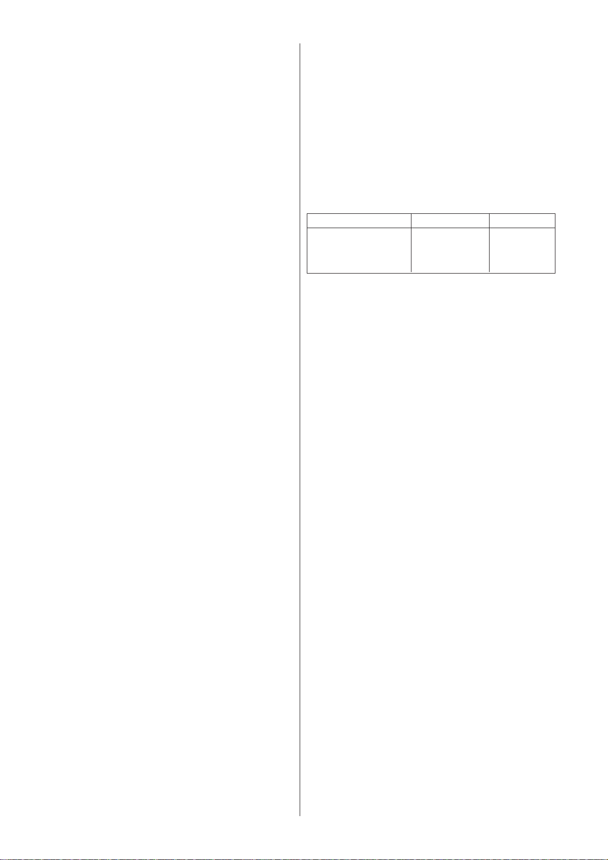
28
Bild-in-Bild-Modul PP700
Allgemein
Das Bild-in-Bild-Modul PP700 besteht aus vier separaten
Funktionseinheiten. Dieses sind die Signalschalter icp2
(Video) und icp7 (RGB), der Farbdecoder ICp3 (TDA9141)
und die Basisband-Verzögerungsleitung ICp4 (TDA4665),
die Analog/Digital-Schnittstelle icp5 (SDA9187) für das
eingesetzte Bild sowie der Bild-in-Bild-Prozessor icp6
(SDA9189). Der Bild-in-Bild-Prozessor SDA9189 ermöglicht
vier verschiedene Bildgrößen: 1:4, 1:9, 1:16 und 1:36. Auch
einsogenanntes Multi-Bild-in-Bild ist möglich. Das
bedeutet, daß 9 eingeblendete Bilder gleichzeitig auf dem
Bildschirm erscheinen können, davon 8 Standbilder und
ein normales, bewegtes Bild. Die Position des
eingeblendeten Bildes kann irgendwo auf dem
Bildschirmsein. Die vorhandenen Features des
Fernsehgerätes hängen von der Software ab.
Farbdecoder Icp3
Das Videosignal für das eingesetzte Bild wird dem VideoMatrix schalter ICq1 auf dem Hauptchassis über den
Anschluß Xp1 an den Pins 10 (CVBS/Y) und 9 (Chrominanz)
entnommen. Das CVBS-Signal wird zum Videoschalter icp2
an Pin 15 geführt und von Pin 1 weiter zum CVBSEingangspin 26 des Farbdecoders ICp3 ausgegeben.
Wenn das Eingangssignal ein Y/C-Signal ist, wird das
Chrominanzsignal direktzu Pin 25 des Farbdecoders
geleitet. Der Signalweg des Y-Signals ist dergleiche wie
der des CVBS-Signales. Der Eingangsmodus wird über den
IIC-Busgewählt. Der Decoderschaltkreis entschlüsselt das
CVBS- (oder Y/C-) Signal und erzeugtdie Luminanz- und
Farbdifferenzsignale. Die Farbdifferenzsignale werden
vonden Ausgangspins 1 und 2 zur BasisbandVerzögerungsleitung ICp4 geführt. Dieverzögerten
Farbdifferenzsignale werden zurück an die Eingangspins 3
und 4 geführt, vonwo sie über eine Schalteinheit an die
Ausgangspins 13 (V) und 14 (U) geleitetwerden. Das
verzögerte Luminanzsignal wird über die gleiche
Schalteinheit zumAusgangspin 12 geführt. Die
Arbeitsweise des Farbdecoders TDA9141 ist der des
TDA9143 auf der Hauptplatine sehr ähnlich.
Analog/Digital-Schnittstelle icp5
Die Y-, U- und V-Signale werden dann zur A/D-Schnittstelle
icp5 an die Pins 23(Y), 21 (U) und 19 (V) geleitet. Der A/DWandler wandelt die analogen Signaleunter Verwendung
von 6-bit Flash-Konvertern in digitale Form.
Diedigitalisierten Y- und UV-Signale werden an den Pins
2...7 (Y) und 8...11 (UV) für den Bild-in-Bild-Prozessor
ausgegeben. Der Weißwert der U- und V-Signale ist an den
Mittelwert der Vrefh- (Pin 22)und Vrefl- (Pin 20) Spannungen
geklemmt. Der Schwarzwert des Y-Signals ist an die VreflSpannung geklemmt. DerSchaltkreis besteht aus einem
Taktgeber, der mit dem eingesetzten Bild inBezug auf den
Sandcastle-Impuls an Pin 15 synchronisiert ist. Der
Taktgebersynchronisiert die interne horizontalphasen
gekoppelte Schleife, die aus einem Horizontaltimer,einem
Phasenkomparator und einem spannungsgesteuerten
Oszillator besteht. Diehorizontalphasengekoppelte Schleife
erzeugt den zeilengekoppeltenBild-in-Bild-Systemtakt LL3
(Pin 12) und das interne Chip-Timing. Die Frequenz des LL3Signalesbeträgt 13,5 MHz. Das RC-Netzwerk an Pin 17 filtert
den Ausgang desPhasenkomparators. Der Horizontaltimer
bestimmt auch die Startzeit und dieWeite des internen
Klemmimpulses sowie die Lage des Abtastsignals BLN (Pin
1), das dabei dieHorizontaldauer der Bilddaten am YAusgang festlegt und mit diesem synchronsein muß. Daher
wird das Abstastsignal BLN in gleichem Maße wie das YSignalverzögert.
Bild-in-Bild-Prozessor icp3
Der Bild-in-Bild-Prozessor enthält sämtliche für die Bild-inBild-Funktionerforderlichen Funktionseinheiten wie Horizontal- und Vertikalfilterung (Verkleinerung), Feldspeicher,
RGB-Matrix, D/A-Wandler, Takterzeugung und
Steuerschaltkreise. Das Videosignal der eingesetzten Quelle
in digitalisierter Form wird von derA/D-Schnittstelle icp5
abgenommen. Das digitalisierte Y-Signal wird an diePins
25...30 und das digitalisierte UV-Signal an die Pins 21...24
geleitet.Die Eingangsdaten werden zuerst in der
Eingangssignal-Verarbeitungseinheit dezimiert.
Dasverkleinerte Fenster, das von den eingesetzten
Synchronimpulsen an den Pins 1(VSI) und 32 (HSI) und
vom ermittelten Zeilenstandard erzeugt wird, weist
eineBreite von 576 Pixel für das Luminanzsignal und 144
Pixel für das Chrominanzsignalauf. In vertikaler Richtung
besteht das Fenster aus 252 Zeilen bei einemStandard von
625 Zeilen (204 Zeilen bei einem Standard von 525 Zeilen).
DieGröße des eingesetzten Bildes hängt vom horizontalen
und vertikalen Verkleinerungsfaktor ab.Dieser Faktor
bestimmt die Anzahl der Pixel und Zeilen wie folgt:
Horiz. und vert. Faktor Pixel / Zeile Zeilen / Feld
2 : 1 288 126
3 : 1 192 84
4 : 1 144 63
6 : 1 96 42
Die dezimierten Daten werden anschließend in den
Feldspeicher geschrieben. DieFrequenz des Schreibtaktes
hängt vom Verkleinerungsfaktor (6,75 MHz, 4,5 MHz,3,375
MHz oder 2,25 MHZ) ab. Der Schreibtakt wird vom
zeilengekoppelten Takt (13,5 MHz) an Pin 20 abgezweigt.
Die Frequenz des Lesetaktes beträgt 27 MHz. Der Lesetakt
wird im internenOszillator erzeugt, der durch einen
externen Quarz an den Pins 2 und 3 gesteuert wird und mit
dem Horizontalsynchronimpuls (HSP) an Pin 15 zeilen
gekoppelt wird. Die Synchronisation des Stammkanals wird
durch den gleichen Horizontalsynchronimpuls (Pin 15) und
Vertikalsynchronimpuls an Pin 16 durchgeführt.
Vom Feldspeicher werden die Daten zur AusgangsVerarbeitungseinheit geführt,die Position und Umrahmung
des eingesetzten Bildes bestimmt. Ein besonderer Effekt,
„Wipe in / Wipe out”, ist auch vorhanden. Das eingesetzte
Bild kannabhängig von der Software programmiert
werden, aus der unteren rechten Ecke der Positionfür das
eingesetzte Bild zu erscheinen und wieder dorthin zu
verschwinden.
Schließlich werden die verarbeiteten Daten in den D/AWandlern in analoge Formgewandelt und die Signale
werden an den Pins 8 (R), 9 (G) und 10 (B) an den RGBSchaltericp7 ausgegeben. Das Schnell austastungs signal
wird an Pin 14 ausgegeben undüber den Transistor ttp2
weiter zum RGB-Prozessor auf der Haupt platinegeleitet.
Der Pin 15 (IIC-Bus gesteuerter Ausgang) des Farbdecoders
führt einen hohenPegel aus, der über den Transistor ttp3
zu Pin 5 des RGB-Schalters geführtwird. Ein hoher Pegel
an Pin 5 wählt das Eingangssignal über die Pins 6, 7 und8
und weiter zum Anschluß Wp1. Ist das Fernsehgerät mit
einem VGA-Anschluß ausgestattet, werden die RGBSignale über den Anschluß Xp2 und über die Pins 2, 3 und
4 desRGB-Schalters zum Anschluß Wp1 eingegeben. Dann
ist die Spannung an Pin 5 desRGB-Schalters niedrig. Wird
die Bild-in-Bild-Funktion im VGA-Modus benutzt, wird der
Pin 5 durch das Schnellaustastungs signal über den Transistor ttp4 gesteuert. Im VGA-Modus stellt die Software
automatisch sicher, daß sich derRGB-Videoprozessor auf
der Hauptplatine im richtigen Eingangs zustand befindet.
Der FET ttp5 trennt die serielle Datenleitung (SDA) vom
Bild-in-Bild-Prozessor, wenn das Fernsehgerät abgeschaltet
wird. Der Jumper jp36 ist nicht installiert.
Bild-in-Bild-Modul PP710
Das Bild-in-Bild-Modul PP710 ist zusätzlich zu den
Funktionen des PP700 miteinem eigenen Tuner / ZF-Block
ausgestattet. Das ZF-Signal vom Bild-in-Bild-Tuner wird im
ICp1 demoduliert und verstärkt und weiter zu Pin 4 des
Videoschalters icp2 geleitet. Die Eingangswahl (Pins 9 und
10) wird über Pin 4 des Tuners und überden IIC-Bus
gesteuert.
Page 65
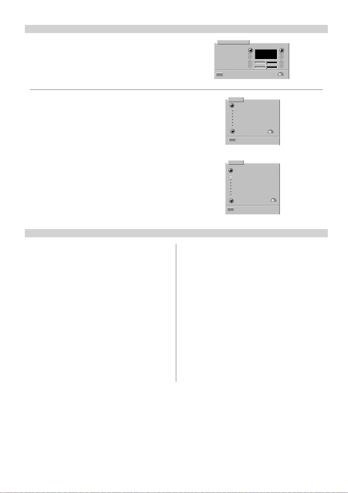
Operating instructions
7
Changing the menu language
1. Press the yellow button to select the Vision menu.
2. Press the red button to select the Display set-up menu.
3. Change the menu language with cursor buttons.
4. Press the OK button to store the changes.
5. Press the TV button to exit.
Manual tuning
1. Select the programme number you want to tune.
2. Press the MENU button.
3. Select “Tuning” and press the OK button.
4. Select “Manual tuning” and press the OK button.
5. Press the red button (Channel search).
6. Press the OK button to store.
7. Press the TV button to exit.
APSi (Automatic Programming System)
1. Press the MENU button.
2. Select “Tuning” and press the OK button.
3. Select “Automatic retuning” and press the OK button.
4. To retune the channels, press the red button.
5. Press the TV button to exit.
Display set-up
Program number
Volume bar
Menu language
Sharpness
Tint
Go back Store ª
Menu
Timers
Front panel lock
Locking
Tuning
Sort programs
Programme settings
Press ª
Go back
Tuning
Automatic retuning
Add new programs
Manual tuning
External units
Copy tuning to VCR
Copy tuning from VCR
Clear all programs
Press ª
Go back
HIDE
SHOW
ENGLISH
Initialization of NVRAM
Initialization of NVRAM (ICf2)
In case that the NVRAM is replaced, it must be initialized
and configured.
1. Switch the TV set to stand-by mode.
Press e- (volume minus) button on local control unit
and at the same time start entering password: MENU,
TV and i with the remote control. Release e- button
after the MENU button is pressed. The record led will
light up to indicate that service mode is enabled.
2. Press the RED-button to pre-configure the set. Green
led will flash once to indicate this.
3a. At the same time the controller will check NVRAM
and initialize it automatically if it was “empty”.
Initializing will take about 15 s. When it is completed,
the green led will light up. Continue to step 4.
3b.Automatic initialization did not happen if the green
led does not light up steadily. In some cases the led
might also light up immediately after configuration
without any initializing, depending on NVRAM
contents. In this case it might be enough to store the
new configuration by pressing “OK”. Continue to
step 4.
3c. If automatic initialization did not happen, you can
start it manually by entering the key code: BLUE (wait
approx. 2 s.), 2, 5, 4 (wait approx. 2 s.) and OK.
Initializing will take about 15 s.
4. Switch off the receiver by pressing the mains switch.
5. Start the receiver in TV mode by pressing the mains
switch. Tune in one or more tv channels.
6. Switch off the receiver with remote control.
7. Enter service mode and make the service adjustments
(see section "SERVICE ADJUSTMENTS VIA I
2
C BUS").
8. Switch off the receiver by pressing the mains switch.
Page 66
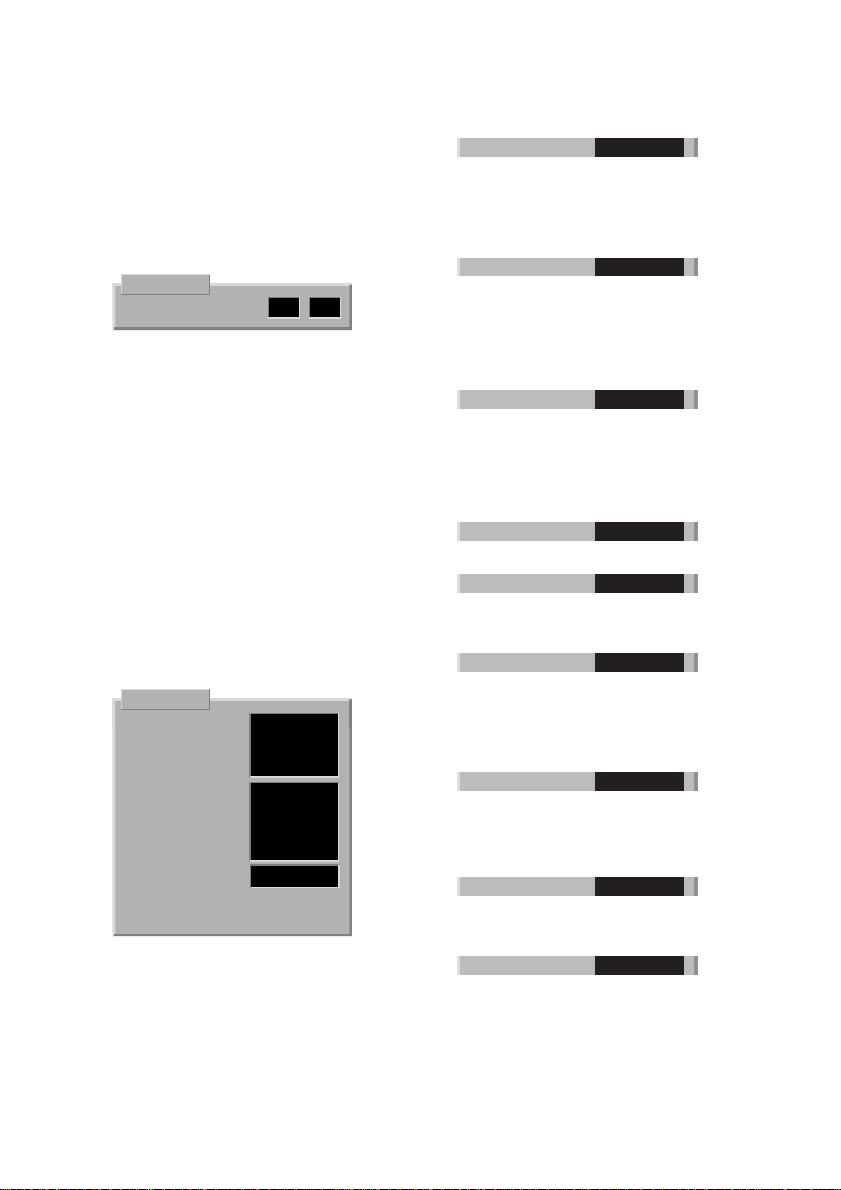
8
Service␣ mode␣ selection
1. Switch the TV set to stand-by mode.
2. Press e- (volume minus) button on local control unit
and at the same time start entering password: MENU,
TV and i with remote control. Release e- button after
the MENU button is pressed. The record led will light
up to indicate that service mode is enabled.
3. Switch on the receiver by pressing the TV button twice
and select service mode by pressing the i button.
SERVICE
00 V-AMPL. 38 36
In service mode an adjustment menu is shown on the
screen.The adjustment number and name, initializing
(left) and adjustment (right) values are shown in the
menu.
4. Exit service mode by switching off the receiver with
the mains switch.
Configuration and fault diagnosis
The set must be configured after adding or removing
some options. By pressing the RED button in service
mode, the processor checks the configuration of the TV
set and shows the settings on the screen. The
configuration can be stored by pressing the OK button.
This feature can also be used in fault diagnosis. If an
option bit is not ’1’ when it should be, the IC (or feature)
is either not present or faulty.
Changing the option bytes
1. Select the configuration mode by pressing the RED
button in service mode.
SERVICE
IIC DEV 1 11111001
IIC DEV 2 00000110
IIC DEV 3 00010100
IIC DEV 4 00000001
IF OPT 00000001
TXT OPT 00000001
SYS OPT 1 00111111
SYS OPT 2 00000000
DSP OPT 00000000
UIF FLAGS 00110010
SW VER. MCABxx.x
NVM VER. MCA1-xx
SW VER. = µP software version.
NVM VER. = NVM software version.
2. Select IIC Device byte 1 - 4, Option byte 1 - 5 or uif
flags byte with cursor button (up-/downwards).
Selected byte is shown highlighted.
3. Set the bits with number buttons (0 ... 7).
4. Store the settings by pressing the OK button.
5. Return to normal service mode by pressing the RED
button.
Option byte description
Bit Description ‘1’ ‘0’
76543210
IIC DEV 1 11111001
0 TV tuner Yes No
1 IF Output, HEF4094 Yes No
3 Decoder synch. processor, TDA9143 Yes No
4 Deflection controller, TDA9151 Yes No
5 RGB processor, TDA4780 Yes No
6 IQTV processor Yes No
7 DPLL Yes No
IIC DEV 2 00000110
0 VGA Yes No
1 Main video switch, TDA6417 Yes No
2 Audio processor, MSP3410 Yes No
3 16:9 picture tube Yes No
4 Comb filter Yes No
5 PIP processor, SDA9188 + TDA9141 Yes No
6 PIP tuner Yes No
7 SCART 3 installed Yes No
IIC DEV 3 00010100
0 Virtual sound (3D Sound) Yes No
1 Dolby processor Yes No
2 SDA30C264 processor Yes No
3 Subwoofer Yes No
4 Megatext, SDA5273/75 Yes No
5 External text memory Yes No
6 Level 2.5 Megatext Yes No
7 One field memory (DB711 Module) Yes No
IIC DEV 4 00000001
0 Nicam enabled Yes No
1 Control lead (Xata) to AR7xx module Yes No
IF OPT 00000001
0 B/G system Yes No
1 I system Yes No
2 D/K system Yes No
3 L/L’ system Yes No
TXT OPT 00000001
0 Top enabled Yes No
1 Flof enabled Yes No
2 P26 disabled Yes No
3 Text sync mode Yes No
4 Automatic text subpage rolling Yes No
5 EPG (nexTView) enabled Yes No
6 EPG record enabled Yes No
SYS OPT 1 00111111
0 E0 (A/V connector) installed Yes No
1 E0 S-video Yes No
2 RGB enabled only in E1 Yes No
3 ACI enabled Yes No
4 Micro power supply installed Yes No
5 Carrier mute enabled Yes No
SYS OPT 2 00000100
0 Picture Tilt enabled Yes No
1 Autostart (Hotel TV) Yes No
2 Hitachi VCR remote enabled Yes No
7 Hotel TV functions enabled (manual) Yes No
UIF FLAGS 00110010
0-2 Logo bit
000 = no logo, go direct to APSi
001 = no logo, go to language menu
3 TV set not used before Yes No
4 Volume bar enabled Yes No
5 On screen programme number enabled Yes No
6 Front panel lock Yes No
7 Off timer active Yes No
Page 67
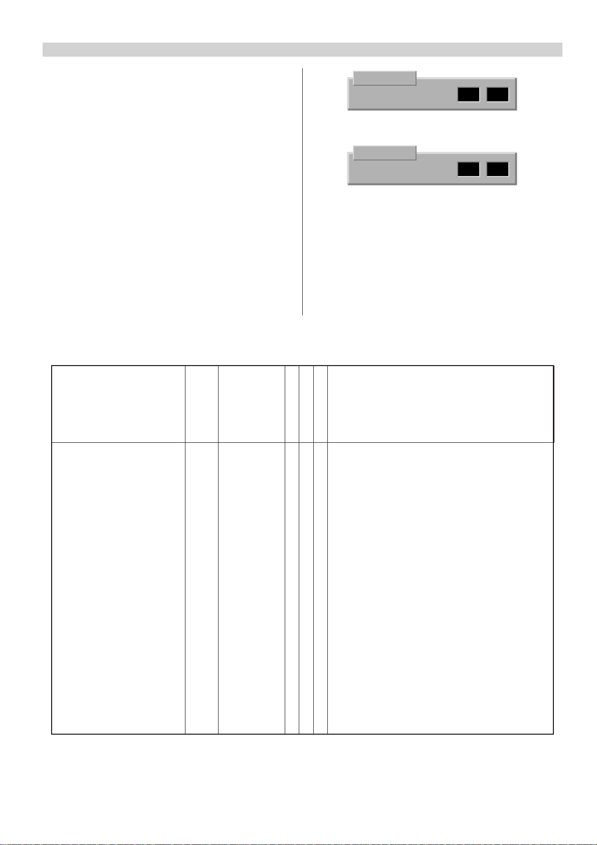
Service adjustments via I2C-bus
9
Remote␣ control␣ buttons␣ in␣ service␣ mode
When the receiver is in service mode you can select the
normal TV mode by pressing the TV button and return to
the service mode by pressing the i button.
Number and cursor buttons are used for service
adjustment. The OK button stores the settings.
Adjustment for different picture format
Make all adjustments with PAL signal unless otherwise
mentioned. First make all adjustments with normal 4:3
picture format. Then make the necessary adjustments
with other picture formats/signals. The required
adjustments are shown in the table below.
Note! Check the configuration of the TV set before
making the adjustments and make only the necessary
adjustments.
Making the service adjustment
1. Give a two numbered code which determines the
adjustment (e.g. 06 = width, see the following tables)
with the number buttons. You can also select the
adjustment with cursor buttons (up-/downwards).
Picture geometry adjustments
SERVICE
06 WIDTH 49 33
2. Adjust with cursor buttons (left/right).
SERVICE
06 WIDTH 49 36
3. Store the new value by pressing the OK button.
Note!
• To avoid incomplete adjustments store each
adjustment in the memory immediately after
adjusting.
• If the adjustment has to be made separately for
different picture format/signal, select the normal user
mode by pressing the TV button and select the desired
picture format/signal. Return to service mode by
pressing the i button.
Adjustment Code OSD name Note!
Vertical amplitude 00 V-AMPL. X X
Vertical off-centre shift 01 V-SHIFT X
Vertical start scan 02 V-START X
Vertical S-correction 03 S-CORR. X X
Vertical slope (coarse) 04 SLOPE-H X Adjust also with NTSC signal.
Vertical slope (fine) 05 SLOPE-L X Adjust also with NTSC signal.
Width 06 WIDTH X
Horizontal shift deflection 07 H-SHIFT X Not in all sets.
Horizontal phase video 08 PHASE X X
Parabola 09 PARABOLA X X
Corner 10 CORNER X X
Trapezium 11 TRAPEZIUM X
EHT compensation 12 EHT X Set brightness and contrast to 90% and
classic (4:3)
wide movie
RGB
compensate the change in picture size.
Page 68
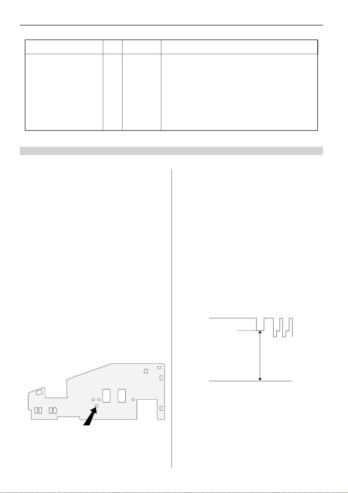
10
Other adjustments
Adjustment Code OSD name
Red reference 18 R REF.
Green reference 19 G REF.
Blue reference 20 B REF.
Red gain 15 R GAIN
Green gain 16 G GAIN
Blue gain 17 B GAIN
Peak white limit 21 PWL
Luma delay 14 LUMA DELAY
Service adjustments
O Power supply block
Supply voltage and protection circuit
1. Set brightness and contrast to normal level. Connect a
universal voltmeter to the cathode of Do11.
2. Adjust the U1 voltage with Ro45. The voltage depends
on the picture tube type, refer to the section “Variable
components”.
Note!
This procedure is necessary e.g. when the picture tube, CRTmodule etc. has been replaced.
Apply a test picture and adjust the R, G and B references.
Then adjust the R, G and B gains.
Normally no need to adjust.
Separate adjustment for Video, PAL BG, PAL DK/I and Secam L.
K Horizontal deflection block
Horizontal linearity
Adjust with Lk2.
Focusing
Set brightness and contrast to normal level. Use
crosshatch pattern and adjust the picture for optimum
resolution.
3. Check the over-current protection after making any
service operations in the primary circuit of the power
supply. Activate the service mode and then switch the
set to stand-by mode. Short circuit the cathode of
Do13 to the ground and keep the short circuit
connected. When the over-current protection works
correctly, the power supply will try to start 2-3 times
before it stops permanently. Remove the short circuit
and switch on the receiver by pressing the mains
button.
SR Tuner/IF module (Frontend)
Tuner AGC
The tuner AGC is adjusted with a potentiometer through
a hole in the heat sink (see picture below).
Apply a 1 mV (60 dBµV) test signal and adjust the picture
just without noise.
81403760
(Screen grid voltage) Ug2 voltage
1. Set brightness and colour saturation to normal level
and contrast to minimum.
2. At the end of the vertical blanking, there is a black
current measurement pulse (clamp pulse) at pin 9 of
ICh1, ICh2 and ICh3. Use an oscilloscope and find the
output stage with the highest cut-off (i.e. the highest
voltage during the black current measurement pulse).
3. Adjust the voltage of the clamp pulse to +140 V with
Ug2 (see figure).
clamp pulse
140 V
0 V
Note! Adjust the voltage with a clamp pulse.
AGC
Page 69
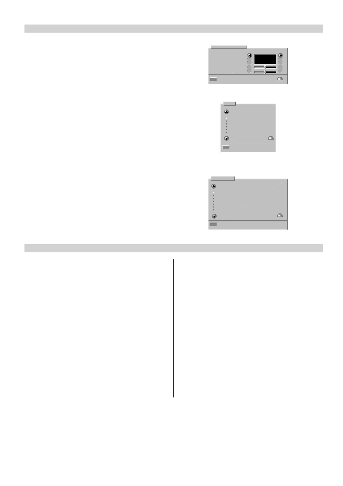
Bedienungsanleitung
11
Ändern der Menüsprache
1. Drücken Sie die gelbe Taste zur Wahl des Bildmenüs.
2. Drücken Sie die rote Taste zur Wahl des AnzeigeOptionen-Menüs.
3. Ändern Sie die Menü Sprache mit den Cursortasten.
4. Drücken Sie zum Speichern der Änderungen die OKTaste.
5. Drücken Sie zum Verlassen des Menüs die TV-Taste.
Manuelle Abstimmung
1. Wählen Sie die Programmnummer, die Sie abstimmen
möchten.
2. Drücken Sie die MENU-Taste.
3. Wählen Sie “Abstimmung” und drücken Sie die OK-Taste.
4. Wählen Sie “Senderabstimmung” und drücken Sie die
OK-Taste.
5. Drücken Sie die rote Taste (Kanal-Suchlauf).
6. Drücken Sie zum Speichern die OK-Taste.
7. Drücken Sie zum Verlassen des Menüs die TV-Taste.
APSi (Automatisches Programmiersystem)
1. Drücken Sie die MENU-Taste.
2. Wählen Sie “Abstimmung” und drücken Sie die OK-Taste.
3. Wählen Sie “Neuprogrammierung” und drücken Sie die
OK-Taste.
4. Drücken Sie zur Neuabstimmung der Kanäle die rote
Taste.
5. Drücken Sie zum Verlassen des Menüs die TV-Taste.
Anzeige-Optionen
Programm-Nr.
Lautstärke Balken
Menü Sprache
Bildschärfe
Farbton
Zurück Speichern ª
Menü
Timer
Tasten verriegelt
Verriegeln
Abstimmung
Sortieren
Programmeinstellungen
Drücken Sie ª
Zurück
Abstimmung
Neuprogrammierung
Neue TV-Programme suchen
Senderabstimmung
Externe Geräte
Kopiere Abstimminformation zum VCR
Kopiere Abstimminformation vom VCR
Alle Programme löschen
Drücken Sie ª
Zurück
UNSICHTB.
SICHTBAR
DEUTSCH
Initialisierung des NVRAM
Initialisierung des NVRAM (ICf2)
Im Falle eines Austausches des NVRAM muß dieser
initialisiert und konfiguriert werden.
1. Schalten Sie das Fernsehgerät in die
Betriebsbereitschaft.
Drücken Sie die e-Taste (Lautstärke-Minus) an der
Bedieneinheit, während Sie gleichzeitig die Eingabe des
Paßwortes mit der Fernbedienung starten: MENU, TV
und i. Lassen Sie die e-Taste los, nachdem die MENUTaste gedrückt wurde. Die Aufnahme-LED leuchtet auf
und zeigt an, daß der Servicemodus aktiviert ist.
2. Drücken Sie zur Vorkonfiguration des Fernsehgerätes
die rote Taste. Die grüne LED leuchtet zur Kontrolle
einmal auf.
3a. Zur gleichen Zeit überprüft der Controller den NVRAM
und initialisiert ihn automatisch, wenn er “leer” war.
Die Initialisierung dauert ungefähr 15 Sekunden. Wenn
sie durchgeführt worden ist, leuchtet die grüne LED auf.
Fahren Sie mit Schritt 4 fort.
3b. Die automatische Initialisierung wurde nicht
durchgeführt, wenn die grüne LED nicht dauernd
aufleuchtet. In manchen Fällen kann die LED direkt nach
der Konfiguration ohne jede Initialisierung aufleuchten,
abhängig vom Inhalt des NVRAM. In diesem Fall ist es
ausreichend, die neue Konfiguration durch Drücken der
OK-Taste zu speichern. Fahren Sie mit Schritt 4 fort.
3c. Ist die automatische Initialisierung nicht durchgeführt
worden, kann diese manuell durch Eingabe des
Schlüsselcodes gestartet werden: BLAUE (ca. 2
Sekunden warten), 2, 5, 4 (ca. 2 Sekunden warten), und
OK. Die Initialisierung dauert ungefähr 15 Sekunden
4. Schalten Sie das Fernsehgerät durch Drücken des
Netzschalters aus.
5. Schalten Sie das Fernsehgerät durch Drücken des
Netzschalters in den Fernsehbetrieb. Stellen Sie einen
oder mehrere Kanäle ein.
6. Schalten Sie das Fernsehgerät mit der Fernbedienung
aus.
7. Gehen Sie in den Servicemodus und nehmen Sie die
Service-Einstellungen vor (siehe Abschnitt “SERVICEEINSTELLUNGEN ÜBER DEN I2C-BUS”).
8. Schalten Sie das Fernsehgerät mit dem Netzschalter
aus.
Page 70
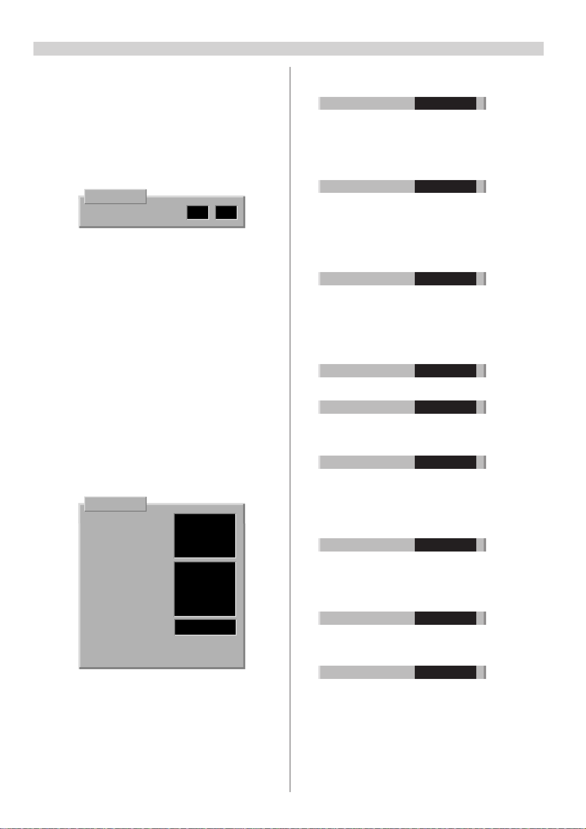
12
Service-Einstellungen
Wahl des Servicemodus
1. Schalten Sie das Fernsehgerät in die Betriebsbereitschaft.
2. Drücken Sie die e-Taste (Lautstärke-Minus) an der
Bedieneinheit, während Sie gleichzeitig die Eingabe des
Paßwortes mit der Fernbedienung starten: MENU, TV
und i. Lassen Sie die e-Taste los, nachdem die MENUTaste gedrückt wurde. Die Aufnahme-LED leuchtet auf
und zeigt an, daß der Servicemodus aktiviert ist.
3. Schalten Sie das Fernsehgerät durch zweimaliges
Drücken der TV-Taste ein und wählen Sie den
Servicemodus durch Drücken der i-Taste.
SERVICE
00 V-AMPL. 38 36
Im Servicemodus wird ein Einstellmenü auf dem
Bildschirm gezeigt. Die Einstellungszahl und der Name,
die Initialisierung (links) und die Einstellwerte (rechts)
werden in diesem Menü gezeigt.
4. Verlassen Sie den Servicemodus durch Ausschalten
des Fernsehgerätes mit dem Netzschalter.
Konfiguration und Fehlerdiagnose
Nach Hinzufügen oder Entfernen von Optionen muß das
Fernsehgerät konfiguriert werden. Durch Drücken der
roten Taste im Servicemodus überprüft der Prozessor die
Konfiguration des Fernsehgerätes und zeigt die
Einstellungen auf dem Bildschirm an. Die Konfiguration
kann durch Drücken der OK-Taste gespeichert werden.
Dieses Feature kann auch bei der Fehlerdiagnose benutzt
werden. Wenn ein Option-Bit nicht ‘1’ ist - was dieses
aber sein sollte - ist der IC (oder das Feature) entweder
nicht vorhanden oder defekt.
Änderung der Options-Bytes
1. Wählen Sie den Konfigurationsmodus durch Drücken
der roten Taste im Servicemodus.
SERVICE
IIC DEV 1 11111001
IIC DEV 2 00000110
IIC DEV 3 00010100
IIC DEV 4 00000001
IF OPT 00000001
TXT OPT 00000001
SYS OPT 1 00111111
SYS OPT 2 00000000
DSP OPT 00000000
UIF FLAGS 00110010
SW VER. MCABxx.x
NVM VER. MCA1-xx
SW VER. = µP Softwareversion.
NVM VER. = NVM Softwareversion.
2. Wählen Sie das IIC-Gerätebyte 1 -4, das Prüfbyte 1 - 5
oder das uif-Kennzeichenbyte mit den Cursortasten
(auf-/abwärts). Das gewählte Byte wird hervorgehoben
dargestellt.
3. Stellen Sie die Bits mit den Zifferntasten (0 ... 7) ein.
4. Speichern Sie die Einstellungen durch Drücken der
OK-Taste.
5. Kehren Sie durch Drücken der roten Taste zum
normalen Servicemodus zurück.
Beschreibungen der Options-Bytes
Bit Beschreibung ´1´ ´0´
76543210
IIC DEV 1 11111001
0 TV-Tuner Ja Nein
1 IF-Ausgang, HEF4094 Ja Nein
3 Synchronprozessor Decoder, TDA9143 Ja Nein
4 Ablenkungssteuerung, TDA9151 Ja Nein
5 RGB-Prozessor, TDA4780 Ja Nein
6 IQTV-Processor Ja Nein
7 DPLL Ja Nein
IIC DEV 2 00000110
0 VGA Option installiert Ja Nein
1 Hauptvideoschalter, TDA6417 Ja Nein
2 Tonprozessor, MSP3410 Ja Nein
3 16:9 Bildröhre Ja Nein
4 Kammfilter installiert Ja Nein
5 PIP-Prozessor, SDA9188 + TDA9141 Ja Nein
6 PIP-Tuner Ja Nein
7 SCART 3 installiert Ja Nein
IIC DEV 3 00010100
0 Virtueller 3D Ton Ja Nein
1 Dolby-Prozessor Ja Nein
2 SDA30C264-Prozessor Ja Nein
3 Subwoofer installiert Ja Nein
4 Megatext, SDA5273/75 Ja Nein
5 VT mit externen RAM Ja Nein
6 Level 2.5 Megatext Ja Nein
7 Einfeld-Speicher (DB711 Modul) Ja Nein
IIC DEV 4 00000001
0 Nicam aktiviert Ja Nein
1 Steuerleitung (Xata) an AR7xx-Modul Ja Nein
IF OPT 00000001
0 B/G-System Ja Nein
1 I-System Ja Nein
2 D/K-System Ja Nein
3 L/L’-System Ja Nein
TXT OPT 00000001
0 Toptext aktiviert Ja Nein
1 Floftext aktiviert Ja Nein
2 TXT packet P26 nicht aktiviert Ja Nein
3 Text-Synchronmodus Ja Nein
4
Autom. Weiterblättern von Textunterseiten
5 EPG (nexTView) aktiviert Ja Nein
6 EPG-Aufnahme aktiviert Ja Nein
Ja Nein
SYS OPT 1 00111111
0 E0 (A/V-Anschluß) installiert Ja Nein
1 E0 S-Video Ja Nein
2 RGB nur möglich bei E1 Ja Nein
3 ACI aktiviert Ja Nein
4 Micro Power Netzteil installiert Ja Nein
5 Tonträger Steuerschaltung Ja Nein
SYS OPT 2 00000100
0 Bilddrehung aktiviert Ja Nein
1 Autostart (Hotel TV) Ja Nein
2 Hitachi VCR Fernbedienung aktiviert Ja Nein
7 Hotel TV-Funktionen aktiviert (manuell) Ja Nein
UIF FLAGS 00110010
0-2 Logo-Bit
000 = Kein Logo, direkt in das APSi gehen
001 = Kein Logo, in das Sprachmenü gehen
3 Fernsehgerät zuvor noch nicht benutzt Ja Nein
4 Lautstärkebalken aktiviert Ja Nein
5 Einblendung Programmnummer aktiviert Ja Nein
6 Verriegelung der Tasten am Gerät Ja Nein
7 Off-Timer aktiv Ja Nein
Page 71
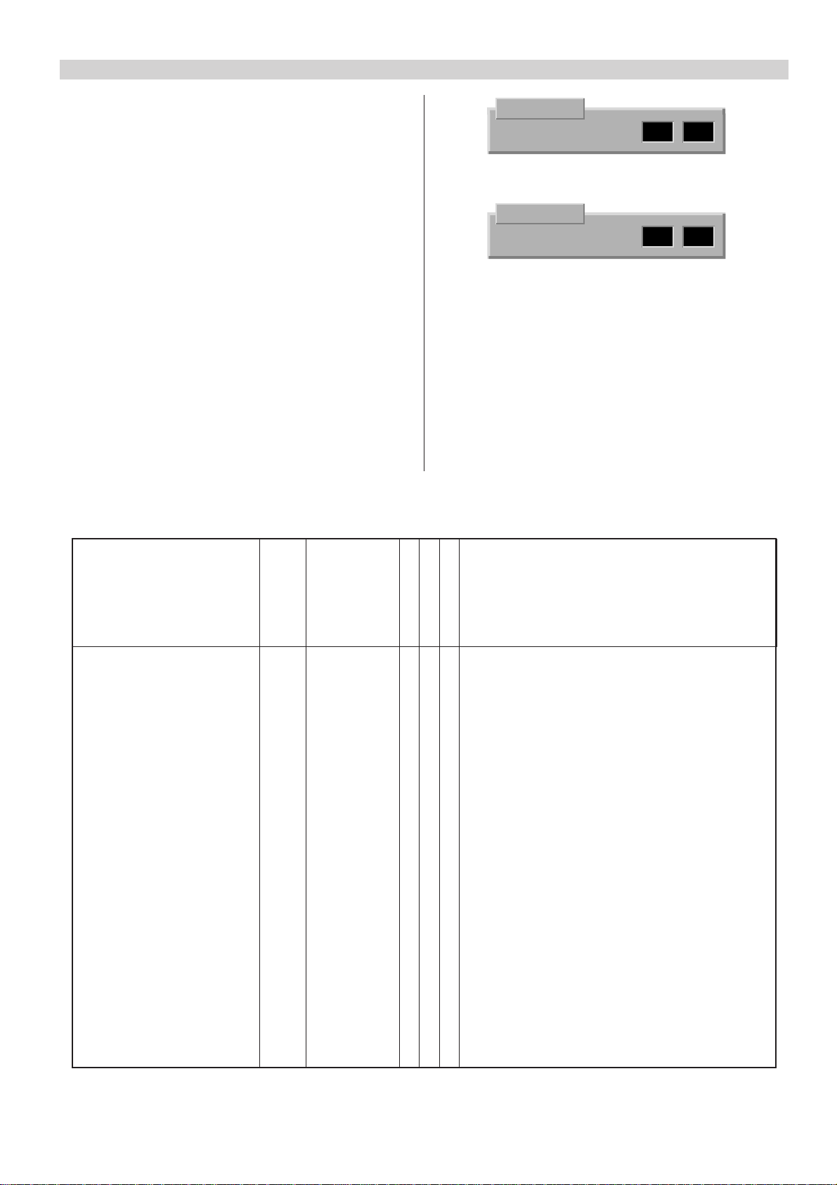
Service-Einstellungen über I2C-bus
13
Tasten der Fernbedienung im Servicemodus
Wenn sich das Fernsehgerät im Servicemodus befindet,
können Sie den normalen Fernsehmodus durch Drücken der
TV-Taste wählen. Sie können durch Drücken der i-Taste zum
Servicemodus zurückkehren. Ziffern- und Cursortasten
werden zur Service-Einstellung benötigt. Die OK-Taste
speichert die Einstellungen.
Einstellungen für ein anderes Bildformat
Wenn nicht anders vermerkt, nehmen Sie alle Einstellungen
mit dem PAL-Signal vor. Führen Sie zuerst alle Einstellungen
mit dem normalen 4:3 Bildformat durch. Führen Sie dann die
notwendigen Einstellungen mit anderen Bildformaten bzw.
Signalen durch. Die erforderlichen Einstellungen werden in
der unten befindlichen Tabelle gezeigt.
Hinweis! Überprüfen Sie die Konfiguration des
Fernsehgerätes, bevor Sie die Einstellungen vornehmen;
nehmen Sie nur die nötigen Einstellungen vor.
Service-Einstellung vornehmen
1. Geben Sie mit den Zifferntasten den zweistelligen Code
ein, der die Einstellung bestimmt (z.B. 06 = Bildbreite,
siehe folgende Tabellen). Sie können die Einstellung auch
mit den Cursortasten wählen (auf-/abwärts).
SERVICE
06 WIDTH 49 33
2. Nehmen Sie die Einstellung mit den Cursortasten
(links/rechts) vor.
SERVICE
06 WIDTH 49 36
3. Speichern Sie den neuen Wert durch Drücken der OKTaste.
Hinweis!
•
Um unvollständige Einstellungen zu vermeiden,
speichern Sie jede Einstellung direkt nach dem
Einstellen ab.
•
Falls die Einstellung getrennt für verschiedene
Bildformate bzw. Signale durchgeführt werden muß,
gehen Sie durch Drücken der TV-Taste in den
normalen Betriebsmodus und wählen Sie das
gewünschte Bildformat bzw. Signal. Gehen Sie durch
Drücken der i-Taste in den Servicemodus zurück.
Einstellungen der Bildgeometrie
OSD
Einstellung Code Bezeichn. Hinweis!
Vertikale Amplitude 00 V-AMPL. X X
Vertikale Lage 01 V-SHIFT X
Vertikale Start-Zeile 02 V-START X
Vertikale S-Korrektur 03 S-CORR. X X
Vertikale Steilheit (grob) 04 SLOPE-H X Auch mit dem NTSC-Signal einstellen.
Vertikale Steilheit (fein) 05 SLOPE-L X Auch mit dem NTSC-Signal einstellen.
Bildbreite 06 WIDTH X
Horizontale Lage der Ablenkung
Horizontale Lage Video 08 PHASE X X
07 H-SHIFT X Nicht in allen Geräten.
Classic
Movie (weit)
RGB
OW-Kissen 09 PARABOLA X X
OW-Ecken Korrektur 10 CORNER X X
OW-Trapez 11 TRAPEZIUM X
EHT-Kompensation 12 EHT X Stellen Sie Helligkeit und Kontrast auf 90%
ein und kompensieren Sie die Änderung
der Bildgröße.
Page 72
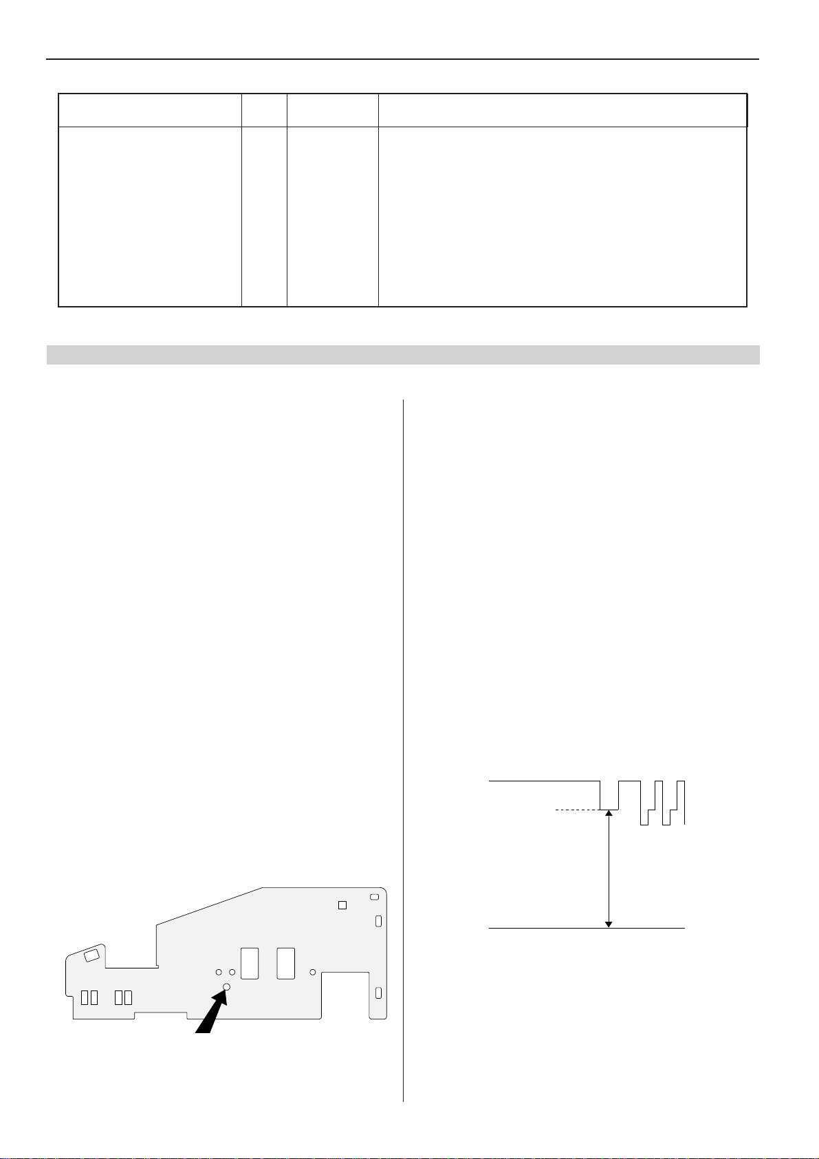
14
Weitere Einstellungen
OSD
Einstellungen Code Bezeichn.
Hinweis!
Rot-Referenz 18 R REF.
Grün-Referenz 19 G REF.
Blau-Referenz 20 B REF.
Rotverstärkung 15 R GAIN
Grünverstärkung 16 G GAIN
Blauverstärkung 17 B GAIN
Oberer Grenzwert weiß 21 PWL
Y-Verzögerungsleitung 14 LUMA DELAY
Service-Einstellungen
O Netzteil
Versorgungsspannung und Schutzschaltung
1. Stellen Sie Helligkeit und Kontrast auf den normalen
Wert ein. Schließen Sie ein Universalvoltmeter an die
Kathode von Do11 an.
2. Stellen Sie die Spannung U1 mit Ro45 ein. Die
Spannung hängt vom Bildröhrentyp ab, siehe auch
Abschnitt “Röhrenabhängige Bauteile”.
3. Prüfen Sie den Überstromschutz nach Durchführung
von Servicearbeiten im primären Schaltkreis der
Stromversorgung. Aktivieren Sie den Servicemodus
und schalten Sie dann das Fernsehgerät in die
Betriebsbereitschaft. Schließen Sie die Kathode von
Do13 an Masse kurz und lassen Sie die
Kurzschlußverbindung bestehen. Wenn der
Überstromschutz richtig arbeitet, versucht die
Stromversorgung 2 - 3 mal zu starten, bevor sie
unterbricht. Entfernen Sie die Kurzschlußschaltung
und schalten Sie das Fernsehgerät durch Drücken des
Netzschalters ein.
Dieser Vorgang ist notwendig, wenn z.B. die Bildröhre, das
CRT-Modul usw. ausgetauscht worden sind. Schalten Sie zu
einem Testbild und stellen Sie die R-, G- und B-Referenzen
ein. Stellen Sie anschließend die R-, G- und B-Verstärkungen
ein.
Braucht normalerweise nicht eingestellt zu werden.
Getrennte Einstellung für Video, PAL BG, PAL DK/I und SECAM L.
K Horizontal-Ablenkeinheit
Horizontale Linearität
Mit Lk2 einstellen.
Fokussierung
Stellen Sie Helligkeit und Kontrast auf den normalen
Wert ein. Benutzen Sie ein Kreuzschraffurmuster und
stellen Sie das Bild auf die optimale Auflösung ein.
(Schirmgitterspannung) Spannung Ug2
1. Stellen Sie Helligkeit und Farbsättigung auf den
normalen Wert und den Kontrast auf den kleinsten
Wert ein.
2. Am Ende des vertikalen Austastens ist ein
Schwarzstrom-Meßimpuls (Klemmimpuls) an Pin 9
von ICh1, ICh2 und ICh3. Verwenden Sie ein
Oszilloskop und ermitteln Sie die Ausgangsstufe mit
dem höchsten Grenzwert (z.B. die höchste Spannung
während des Schwarzstrom-Meßimpulses).
SR Tuner/ZF Modul (Frontend)
AGC-Tuner
Die AGC Regelung des Tuners wird mit einem
Potentiometer durch eine Öffnung im Kühlkörper (siehe
Bild unten) eingestellt.
Geben Sie ein Testsignal von 1 mV (60 dBµV) und stellen
Sie das Bild genau ohne Rauschen ein.
81403760
AGC
3. Stellen Sie die Spannung des Klemmimpulses mit Ug2
auf +140 V ein (siehe Abbildung).
Klemmimpulse
140 V
0 V
Hinweis! Die Spannung auf die Klemmimpulse
einzustellen.
Page 73
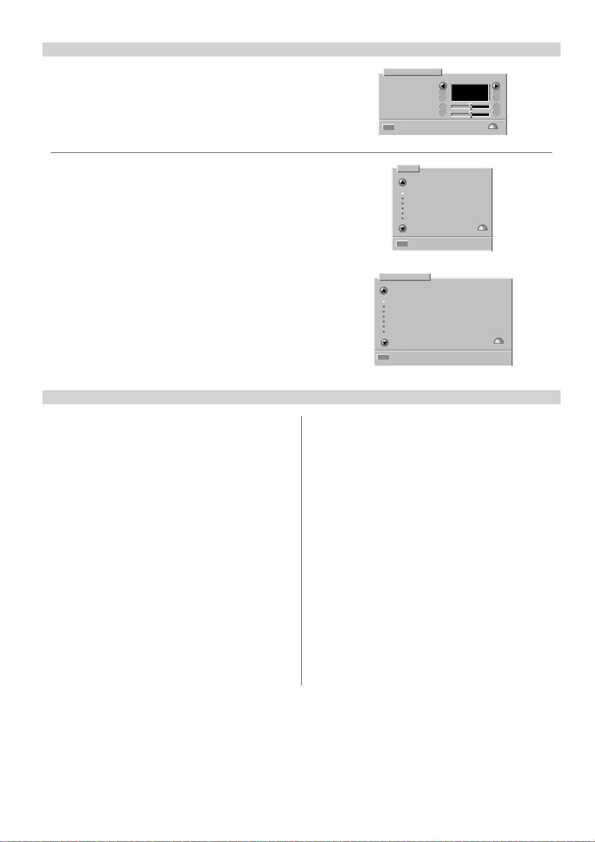
Mode d’emploi
15
Modification de la langue du menu
1. Appuyez sur la touche jaune pour sélectionner le menu Image.
2. Appuyez sur la touche rouge pour sélectionner le menu Affichage
écran.
3. Sélectionnez la langue du menu à l’aide des touches curseurs.
4. Appuyez sur la touche OK pour enregistrer les modifications.
5. Appuyez sur la touche TV pour quitter le menu.
Recherche manuelle
1. Sélectionnez le numéro du programme que vous voulez régler.
2. Appuyez sur la touche MENU.
3. Sélectionnez l’option “Syntonisation” et appuyez sur la touche OK.
4. Sélectionnez l’option “Recherche manuelle” et appuyez sur la
touche OK.
5. Lancez la recherche de canal à l’aide de la touche rouge.
6. Pour mémoriser vos sélections, appuyez sur la touche OK.
7. Appuyez sur la touche TV pour quitter le menu.
Système de programmation automatique (APSi)
1. Appuyez sur la touche MENU.
2. Sélectionnez l’option “Syntonisation” et appuyez sur la touche OK.
3. Sélectionnez l’option “Syntonisation automatique” et appuyez sur
la touche OK.
4. Pour régler les chaînes, appuyez sur la touche rouge.
5. Appuyez sur la touche TV pour quitter le menu.
Affichage écran
Nº de chaîne
Barre de volume
Langue du menu
Netteté
Teinte
Retour Mémoriser ª
Menu
Minuterie
Verrouillage commande
Clé électronique
Syntonisation
Classement des chaînes
Personnalisation
Presser ª
Retour
Syntonisation
Syntonisation automatique
Ajouter de nouvelles chaînes
Recherche manuelle
Sources externes
Copie de la syntonisation vers VCR
Copie de la syntonisation du VCR
Réinitialisation
Presser ª
Retour
INVISIBLE
VISIBLE
FRANCAIS
Initialisation de la NVRAM
Initialisation de la NVRAM (ICf2)
Si la RAM non volatile (NVRAM) est remplacée, elle doit
être initialisée et configurée.
1. Mettez le téléviseur en mode mise en veille.
Appuyez sur la touche e- (abaissement du volume)
de l’unité de commande centralisée et commencez
simultanément à saisir le mot de passe : MENU, TV et i
avec la télécommande. Relâchez la touche e- après
avoir appuyé sur la touche MENU. Le voyant
d’enregistrement s’allume pour indiquer que le mode
maintenance est activé.
2. Appuyez sur la touche rouge pour pré-configurer le
téléviseur. Le voyant vert clignote ensuite une fois.
3a. Pendant ce temps, le contrôleur vérifie la NVRAM et
l’initialise automatiquement si elle est “vide”.
L’initialisation prend environ 15 secondes. Quand elle
est achevée, le voyant vert s’allume. Passez à l’étape 4.
3b. Le voyant vert n’est pas allumé en continu si
l’initialisation automatique ne s’est pas produit. Dans
certains cas, le voyant peut également s’allumer
immédiatement après la configuration sans aucune
initialisation, selon le contenu de la NVRAM. Dans ce
cas, il suffit d’enregistrer la nouvelle configuration en
appuyant sur OK. Passez ensuite à l’étape 4.
3c. Si l’initialisation automatique ne s’est pas produite,
vous pouvez la lancer manuellement en entrant le
code clé : bleu (attendez environ 2 secondes), 2, 5, 4
(attendez environ 2 secondes) et OK. L’initialisation
prend environ 15 secondes.
4. Eteignez le récepteur en appuyant sur l’interrupteur
principal.
5. Lancez le récepteur en mode de réception TV en
appuyant sur l’interrupteur principal. Réglez une ou
plusieurs chaînes de télévision.
6. Eteignez le récepteur avec la télécommande.
7. Entrez en mode maintenance et effectuez les réglages
(reportez-vous à la section “
moyen du bus I2C
”).
Réglages de service au
8. Eteignez le récepteur en appuyant sur l’interrupteur
principal.
Page 74
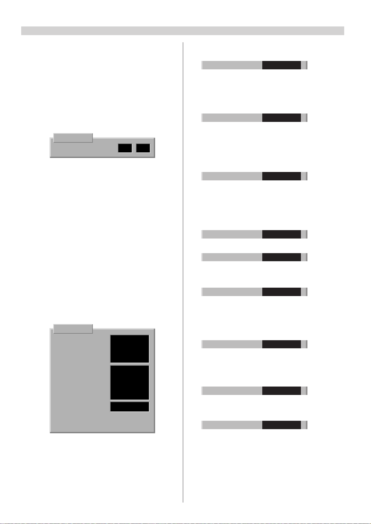
16
Réglages de service
Sélection du mode service
1. Mettez le téléviseur en mode mise en veille.
2. Appuyez sur la touche e- (abaissement du volume) de
l’unité de commande centralisée et commencez
simultanément à saisir le mot de passe : MENU, TV et i
avec la télécommande. Relâchez la touche e- après avoir
appuyé sur la touche MENU. Le voyant d’enregistrement
s’allume pour indiquer que le mode service est activé.
3. Allumez le téléviseur en appuyant deux fois sur la touche
TV et sélectionnez le mode service en appuyant sur la
touche i.
SERVICE
00 V-AMPL. 38 36
En mode maintenance, un menu de réglage apparaît à
l’écran. Le numéro et le nom du réglage, les valeurs
d’initialisation (à gauche) et de réglage (à droite) sont
affichées dans le menu.
4. Quittez le mode maintenance en éteignant le téléviseur
avec l’interrupteur principal.
Configuration et diagnostic de panne
Vous devez configurer le téléviseur après tout ajout ou
suppression d’options. En appuyant sur la touche rouge en
mode service, le processeur contrôle la configuration du
téléviseur et affiche les paramètres à l’écran. Vous pouvez
enregistrer la configuration en appuyant sur la touche OK.
Cette fonction peut également être utilisée pour le
diagnostic de panne. Si un bit d’option n’a pas la valeur ‘1’
comme il devrait l’être, cela signifie que le CI (ou la
fonction) est soit absent, soit défaillant.
Modification des octets d’options
1. Sélectionnez le mode configuration en appuyant sur la
touche rouge en mode service.
SERVICE
IIC DEV 1 11111001
IIC DEV 2 00000110
IIC DEV 3 00010100
IIC DEV 4 00000001
IF OPT 00000001
TXT OPT 00000001
SYS OPT 1 00111111
SYS OPT 2 00000000
DSP OPT 00000000
UIF FLAGS 00110010
SW VER. MCABxx.x
NVM VER. MCA1-xx
SW VER. = version logicielle µP.
NVM VER. = version logicielle NVM.
2. Sélectionnez IIC Device byte 1 - 4, Option byte 1 - 5 ou uif
flags byte avec la touche curseur (vers le haut/vers le
bas). L’octet sélectionné apparaît en surbrillance.
3. Définissez les bits à l’aide des touches numériques (0 ... 7).
4. Mémorisez les paramètres en appuyant sur la touche OK.
5. Retournez en mode service normal en appuyant sur la
touche rouge.
Descriptions des octets d’option
Bit Description ‘1’ ‘0’
76543210
IIC DEV 1 11111001
0 Tuner TV oui non
1 Sortie FI, HEF4094 oui non
3 Processeur synchro décodeur, TDA9143 oui non
4 Contrôleur déflexion, TDA9151 oui non
5 Processeur RVB, TDA4780 oui non
6 Processeur IQTV oui non
7 DPLL oui non
IIC DEV 2 00000110
0 VGA oui non
1 Interrupteur vidéo principal TDA6417 oui non
2 Processeur Son, MSP3410 oui non
3 Tube 16:9 oui non
4 Filtre-peigne oui non
5 Processeur PIP, SDA9188 + TDA9141 oui non
6 Tuner PIP (image dans l’image) oui non
7 SCART 3 installé oui non
IIC DEV 3 00010100
0 Son virtuel (3D Sound) oui non
1 Processeur Dolby oui non
2 Processeur SDA30C264 oui non
3 Subwoofer oui non
4 Megatext, SDA5273/75 oui non
5 Mémoire texte externe oui non
6 Megatext Level 2.5 oui non
7 Mémoire un champ (Module DB711) oui non
IIC DEV 4 00000001
0 Nicam activé oui non
1
Ligne de commande (Xata) au module AR7xx
oui non
IF OPT 00000001
0 Système B/G oui non
1 Système I oui non
2 Système D/K oui non
3 Système L/L’ oui non
TXT OPT 00000001
0 TOP text activé oui non
1 Flof text activé oui non
2 P26 activé oui non
3 TXT accrochage mode oui non
4 TXT souspage défilement oui non
5 Fonction EPG (nexTView) activée oui non
6 Fonction d’enregistrement EPG activée oui non
SYS OPT 1 00111111
0 E0 (connecteur A/V) installé oui non
1 Vidéo S (E0) oui non
2 RVB uniquement activé dans E1 oui non
3 Fonction ACI activée oui non
4 Alimentation micro installée oui non
5 Blocage de porteuse activé oui non
SYS OPT 2 00000000
0 Rotation activé oui non
1 Démarrage automatique (TV hôtel) oui non
2 Télécommande du magnétoscope activée oui non
7 Fonctions TV hôtel activées (manuel) oui non
UIF FLAGS 00110010
0-2 Bit de logo
000 =
pas de logo, aller directement à la fonction APSi
001 =
3 Téléviseur non utilisé auparavant oui non
4 Barre de volume activée oui non
5 Numéro de programme activé à l’écran oui non
6 Verrouillage du panneau avant oui non
7 Compteur d’arrêt actif oui non
pas de logo, aller au menu Langue
Page 75
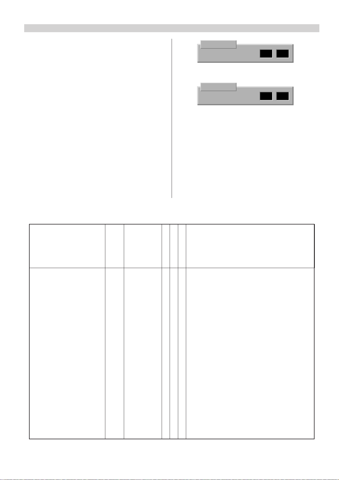
Réglages de service au moyen du bus I2C
17
Touches de la télécommande en mode service
Quand le récepteur est en mode service, vous pouvez
sélectionner le mode de réception TV normal en appuyant
sur la touche TV et retourner au mode service en appuyant
sur la touche i. Les touches numériques et les touches
curseurs sont utilisés pour le réglage de service. La touche
OK permet de mémoriser les paramètres.
Réglages pour un format d’image différent
Sauf indication contraire, effectuez tous les réglages avec
le signal PAL. Commencez par effectuer les réglages avec
le format d’image normal 4:3. Ensuite, procédez à tous les
réglages nécessaires avec les autres signaux et formats
d’image. Les réglages requis sont décrits dans le tableau
ci-dessous.
Remarque ! Contrôlez la configuration du téléviseur avant
de procéder aux réglages et n’effectuez que ceux qui sont
indispensables.
Réalisation des réglages de service
1. Définissez un code à deux chiffres pour déterminer le
réglage (par ex. 06 = largeur E-O, voir les tableaux
suivants) à l’aide des touches numériques. Vous pouvez
également sélectionner le réglage avec les touches
curseurs (vers le haut/vers le bas).
SERVICE
06 WIDTH 49 33
2. Procédez au réglage avec les touches curseurs
(gauche/droite).
SERVICE
06 WIDTH 49 36
3. Mémorisez la nouvelle valeur en appuyant sur la
touche OK.
Remarque !
•
Pour éviter les réglages incomplets, enregistrez
chaque réglage en mémoire immédiatement après
l’avoir effectué.
•
Si le réglage doit être réalisé séparément pour chaque
signal et format d’image différent, sélectionnez le
mode utilisateur normal en appuyant sur la touche de
réception TV et sélectionnez le signal et format
d’image de votre choix. Revenez en mode service en
appuyant sur la touche i.
Reglages géométrique d’image
Réglage Code Nom OSD Remarque !
Amplitude verticale 00 V-AMPL. X X
Décentrage vertical 01 V-SHIFT X
Balayage vertical 02 V-START X
Correction S Verticale 03 S-CORR. X X
Dent de scie vert. (grossière) 04 SLOPE-H X
Dent de scie vert. (précise) 05 SLOPE-L X
Largeur E-O 06 WIDTH X
Phase horizontale déflexion 07 H-SHIFT X Ne concerne pas tous les téléviseurs.
Phase horizontale vidéo 08 PHASE X X
Parabole E-O 09 PARABOLA X X
classique (4:3)
cinemascope
RVB
Effectuez aussi le réglage avec le signal NTSC.
Effectuez aussi le réglage avec le signal NTSC.
Coin E-O 10 CORNER X X
Déformation trapézoïdale E-O
Compensation EHT 12 EHT X Portez la lumiére et le contraste à 90% et
11 TRAPEZIUM X
compensez le changement dans la taille
de I’image.
Page 76
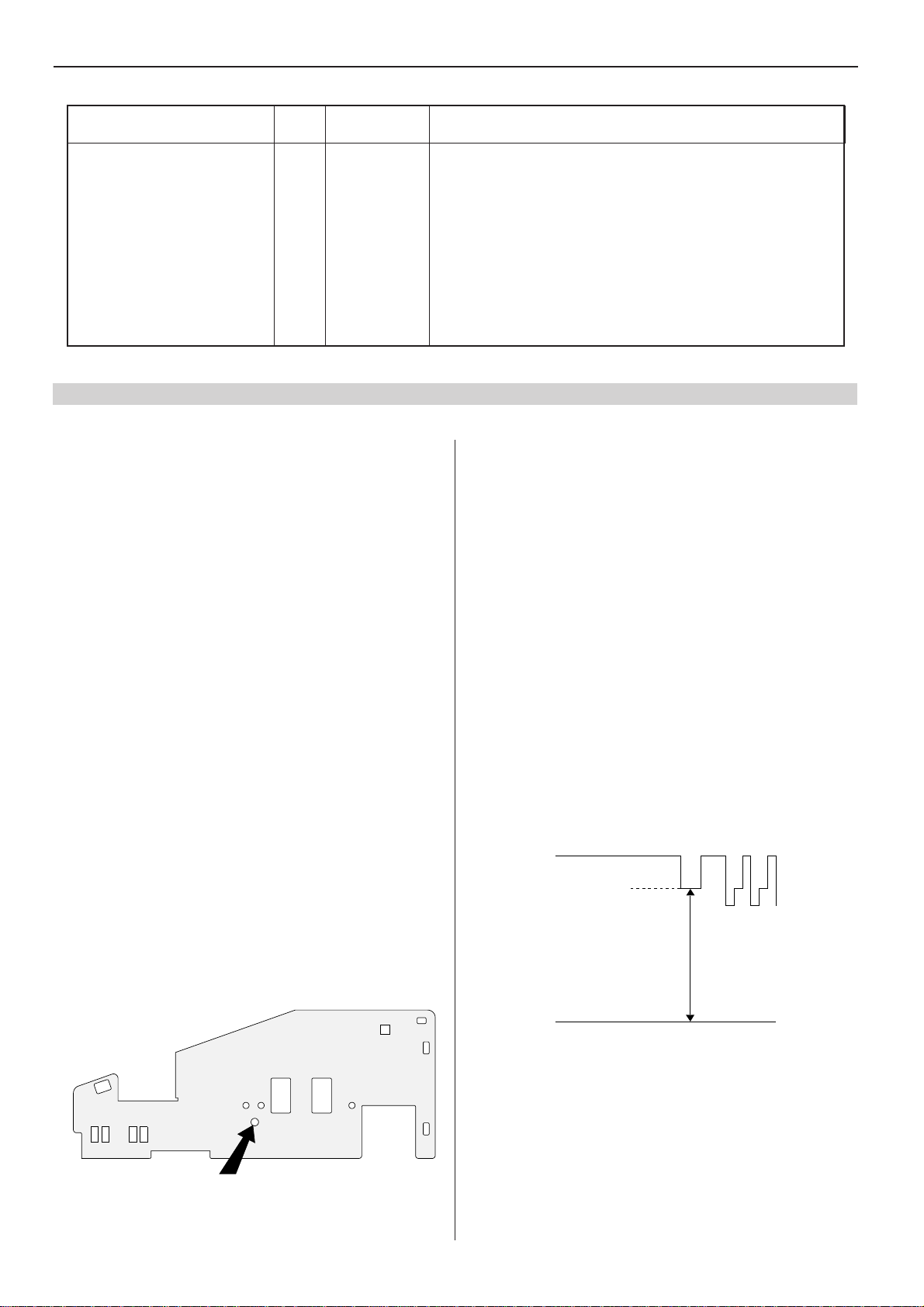
18
Autres réglages
Réglage Code Nom OSD
Référence rouge 18 R REF.
Référence vert 19 G REF.
Référence bleu 20 B REF.
Amplification rouge 15 R GAIN
Amplification vert 16 G GAIN
Amplification bleu 17 B GAIN
Seuil des crêtes de blanc 21 PWL
Délai de luminance 14 LUMA DELAY
Réglages de service
O Bloc d’alimentation
Tension d’alimentation et circuit de protection
1. Réglez la luminosité et le contraste à un niveau
normal. Branchez un voltmètre universel à la cathode
Do11.
2. Réglez la tension U1 avec Ro45. La tension dépend du
type de tube image du téléviseur ; reportez-vous à la
section “Composants variables”.
3. Contrôlez le dispositif de protection contre les
surcharges après toute opération de maintenance
dans le circuit principal de l’alimentation. Activez le
mode maintenance, puis mettez le téléviseur en mode
mise en veille. Court-circuitez la cathode Do13 à la
masse et maintenez le court-circuit connecté. Quand le
dispositif de protection contre les surcharges
fonctionne correctement, l’alimentation est stoppée
définitivement après trois tentatives. Supprimez le
court-circuit et allumez le récepteur en appuyant sur le
bouton d’alimentation.
Remarque !
La procédure est nécessaire lorsque, par exemple, le tube
image ou le module CRT a été remplacé.
Appliquez une mire et réglez les références R, V et B. Réglez
ensuite les amplifications R, V et B.
Normalement pas besoin de régler.
Réglage distinct pour Vidéo, PAL BG, PAL DK/I et Secam L.
K Bloc de déflexion horizontale
Linéarité horizontale
Effectuez le réglage avec Lk2.
Mise au point
Définissez la luminosité et le contraste à un niveau
normal. Utilisez la mire de quadrillage et réglez l’image
pour une résolution optimale.
(Tension de la grille-écran) Tension Ug2
1. Définissez la luminosité et la saturation couleur à un
niveau normal ainsi que le contraste à un niveau
minimum.
2. A la fin de de la suppression de trame, apparaît une
impulsion de mesure du niveau de noir à la broche 9
de ICh1, ICh2 et ICh3. Utilisez un oscilloscope pour
trouver l’étage de sortie avec la coupure la plus élevée
(c’est-à-dire la tension la plus élevée pendant
l’impulsion de mesure du niveau de noir).
3. Réglez la tension des Ug2 à +140 V (voir l’illustration).
SR Tuner/Module IF (Frontend)
Tuner CAG
Le tuner CAG se règle avec un potentiomètre par un trou
dans le dissipateur thermique (voir illustration ci-dessous).
Appliquez un signal de mesure de 1 mV (60 dBµV) et
réglez la netteté de l’image pour qu’elle ne contienne
aucun parasite.
81403760
AGC
Clamp
140 V
0 V
Remarque ! Réglez la tension avec le clamp.
Page 77
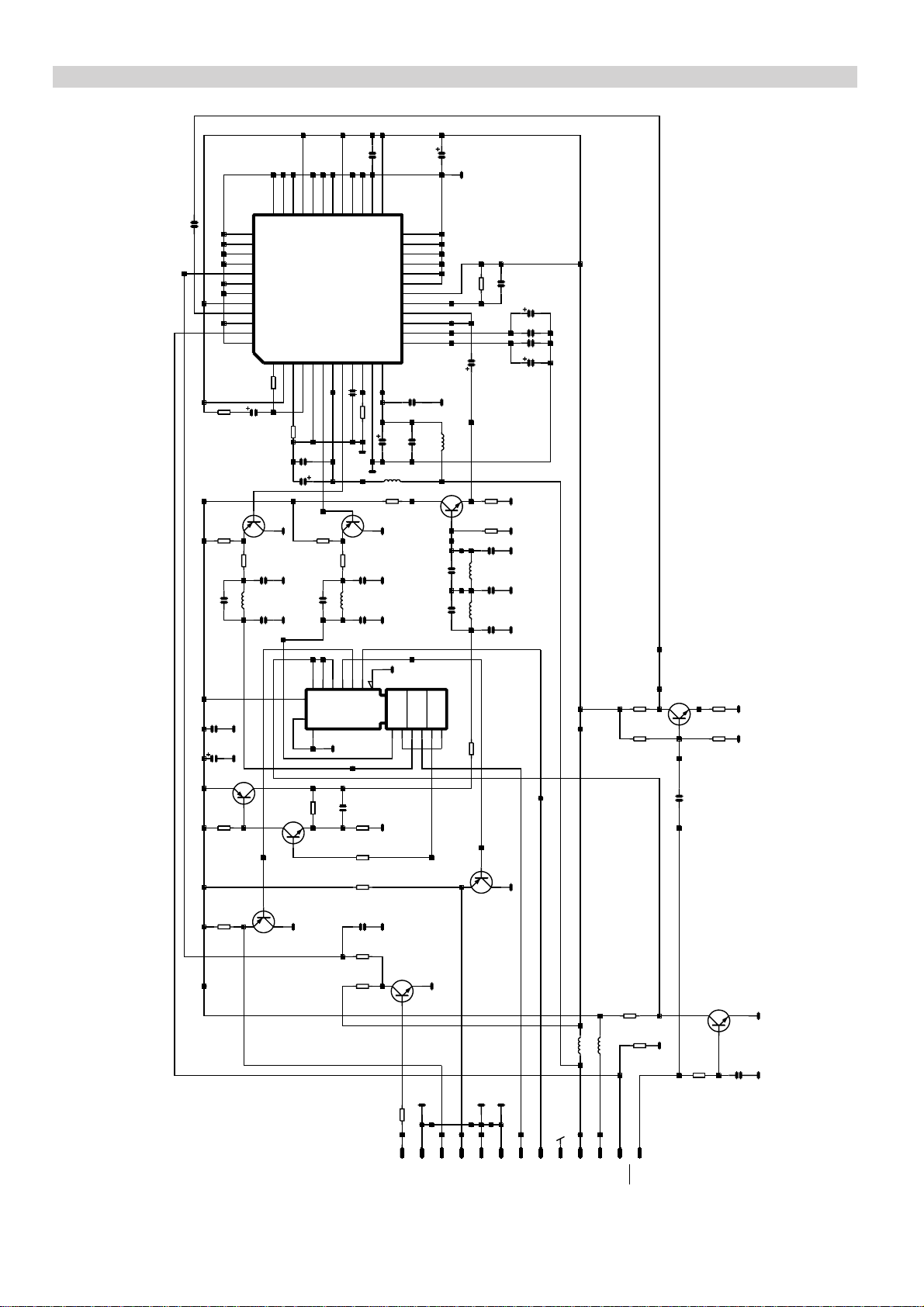
20
CF700 Comb filter module
100 n
cc3 2
282930
36
cc2 9
100 n
37
38
39
40
41
42
43
44
45
46
47
48
123456789
51R
rc4 9
10u
rc4 8
100 R
Cc4 7
rc4 4
2k2
tc1 2
rc4 5
330 R
22p
cc4 3
10u
8p2
Lc7
cc4 1
cc4 2
68p
3132333435
27
26
25
icc 2
MC1 4 162 7
101112
cc4 8 1 00n
10k
39k
rc3 9
cc1 8
100 n
47u
Cc1 7
A
BC8 5 7B
A
cc4 4
A
rc1 8
A
BC8 5 7B
rc4 6
8p2
tc1 1
2k2
rc4 7
Lc 8
A
330 R
cc4 6
22p
A
10 u
cc4 5
68p
A
47u
Cc3 3
D
24
23
22
21
20
19
18
17
16
15
14
13
cc 2 0
100 n
A
Cc2 1
47u
cc2 2
100 n
Lc6
15u
rc2 4
100 R
tc9
BC8 4 7B
cc3 5
cc3 6
cc3 1
470 n
82 0 k
rc1 9
10u
Cc2 7
cc2 6
100 n
cc2 8
47u
Cc2 3
15u
Lc5
A
rc2 3
470 R
560 R
rc1 7
A
AA
cc3 7
56p
Lc3
10u
68p
cc3 8
6u8
Lc4
56p
A
cc3 9
100 n
10u
Cc2 4
(no t
in u se)
(no t
in u se)
A
6
9
10SB15
14
11
VC C
SA
16
100 n
cc1 3
A
47u
cc1 2
A
1k0
rc1 2
tc8
rc8
2k2
8
GND
7
VEE
560 R
rc1 4
BC8 5 7B
tc7
BC8 4 7B
BC8 5 7B
tc4
E*
ZB4ZC
ZA
SC
Y0 B
Y1 A1Y1 B
Y0 A
A
10p
cc1 1
12
390 R
rc1 3
A
470 R
rc1 1
rc9
2k2
cc3
10p
D
100 R
rc4 3
rc7
10k
rc6
220 R
Xc1 - 13
Y1 C
Y0 C
icc 1
2
13
BC8 4 7B
tc3
O M / B Y P A S S
HCF 4 053 B
3
5
rc1 6
220 R
BC8 5 7B
tc6
A
Lc1
15u
Lc2
D A
NC
S C
G N D
G N D
G N D
Y _ o u t
C _ o u t
C _ i n
+ 5 V
Y _ i n
rc1 5
rc3
rc4 1
10k
rc4 2
15u
+ 1 2 V
P A L / N T S C
BF5 9 9
tc5
1k2
10 k
cc5
47k
D
Xc1 - 1
C L O C K / S V H S
rc 2 0
18 0 R
D
3k3
rc4
D
1n0
BC8 4 7B
tc1 0
100 n
cc4 0
rc4 0
6k8
D D
Page 78
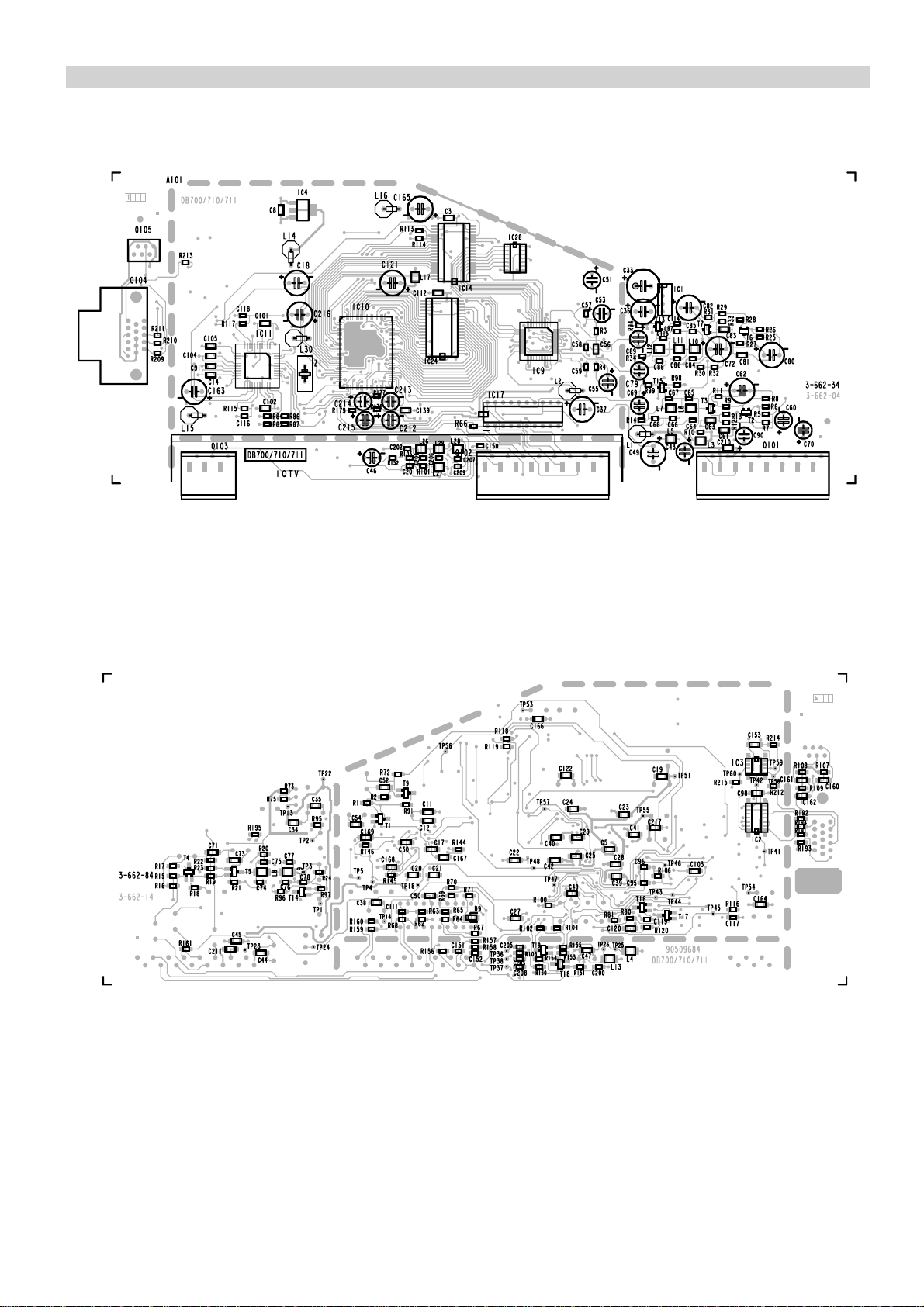
DB700/710 Feature module
21
Page 79
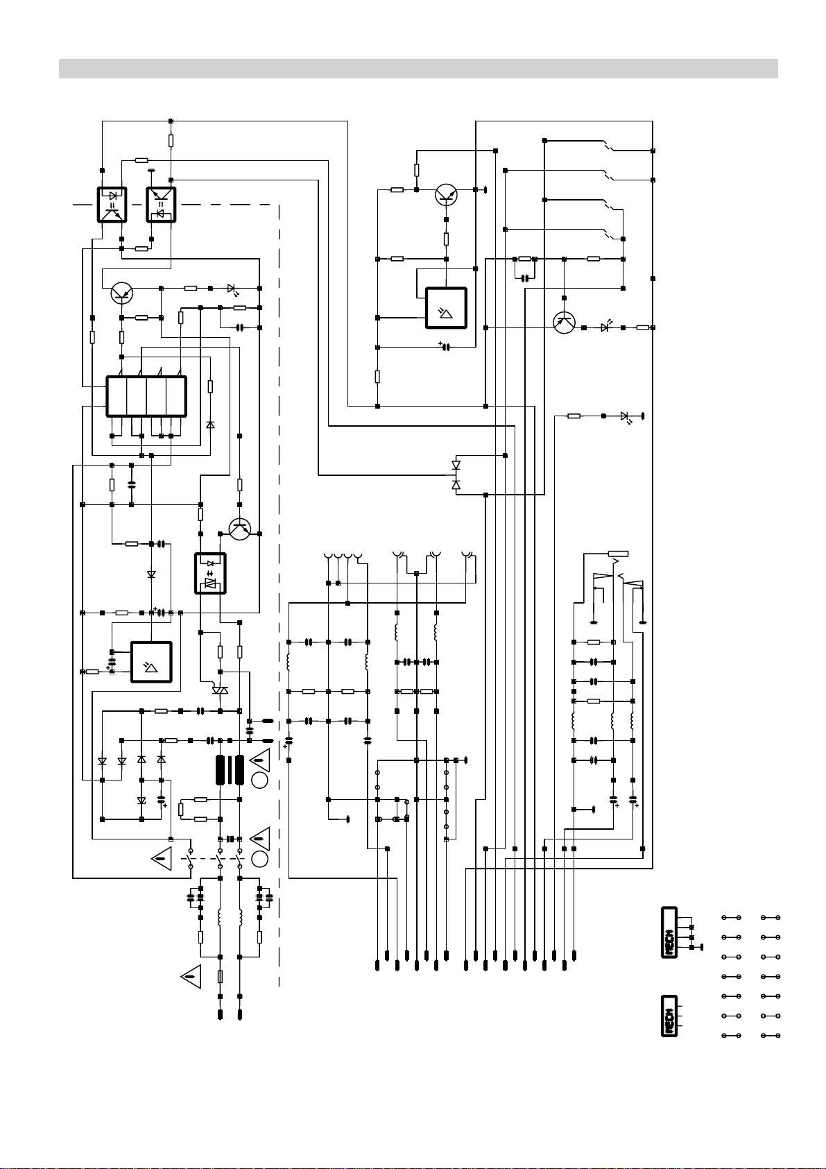
FC700 Control module
rfc4 6
100k
1k0
rfc4 3
TCD T 1 101
ICfc 3
ICfc 4
TCDT 1 1 01
23
SWf c 4
rfc1 2
1k0
BC84 7 B
tfc3
10k
rfc 1 5
SWfc 2 SWfc 3
tfc6
BC85 7 B
rfc 3 8
1k0
GND
7
Vcc
14
11A62B83A124A134B9
rfc3 3
560k
22u
Cfc2 7
1k0
Rfc 2 8
Dfc7
BY52 7
Dfc6
&
21B5
rfc 2 9
BY52 7
rfc4 1
1k0
LS54 2 0 R
1k8
rfc4 2
rfc5 3
47k
rfc5 1
100k
rfc3 9
10k
42Y3
10
11
3Y
1Y
2A
560k
rfc3 4
Dfc 1 2
4k7
1
2
BY52 7
Dfc8
DZfc 1
ZPD5 . 1
4Y
3B
HEF4 0 1 1BP
ICfc 1
100n
cfc3 1
1k0
rfc3 1
cfc2 9
100n
LL41 4 8
Cfc2 8
10u
3
OUT
GND
VCC
Hfc2
SFH 5 0 6
Cfc2 6
220R
220R
Rfc2 3
Rfc2 4
Dfc9
BY52 7
rfc4 9
1M8
220u
Cfc2 3
1M8
rfc4 8
Ufc1
Dfc1 6
1M0
rfc5 2
100n
cfc3 6
rfc5 0
1k8
dfc1 3
LL41 4 8
rfc 3 7
tfc 1
IL4 1 0
(icf c 5 )
ICfc 2
Rfc2 6
Rfc2 7
100R
BT13 7 _ 600
Dfc1 1
330 n
Cfc2
Cfc2 4
330n
MFC1
29m
~
Cfc1
100n
250V
1M8
rfc4 5
M A I N S I S O L A T E D
M A I N S N O N I S O L A T E D
10k
BC84 7 B
Xfc9 - 1
Xfc9 - 3
Xfc9 - 2
(TLP 1 6 8J)
cfc1 3
390p
cfc1 0
100R
Lfc5
2u2
rfc4
75R
rfc3
~
cfc9
XO2- 2
250V
100 n
10u
Cfc8
XO2- 1
x
x
390p
390p
cfc1 2
VIDE O _ G ND
rfc1 6
rfc 1 3
330 R
Xfc9 - 4
Xfc 6 - 1
390p
10u
Lfc3
2u2
Lfc 6
75R
1n0
cfc1 1
J13
jfc1 4
100k
rfc1 4
15k
-38
3
1
OUT
GND
Hfc1
SFH5 0 6
2
VCC
10u
Cfc2 0
BAV 7 0
dfc1 8
Xfc 6 - 3
Xfc 6 - 2
10u
Lfc4
4n7
4n7
cfc5
cfc7
rfc2
47k
47k
rfc 1
AUDI O _ GND
jfc1 5
jfc1 7 jfc 1 6
47k
rfc1 0
10n
cfc 3 2
BC85 7 B
tfc2
rfc4 7
10n
cfc1 9
10n
cfc 1 8
Lfc9
10u
10n
cfc1 7
10n
cfc1 6
rfc1 1
15k
Dfc4
1k0
Xfc1 0
54326
1
10k
rfc2 0
10k
rfc1 9
Lfc7
Cfc1 4
HP_G N D
SWfc 1
LS54 6 0
270 R
rfc9
LG5 4 6 0
Dfc1 7
7
Lfc8
10u
10u
100u
Cfc1 5
100u
15p
Cfc2 1
15p
cfc3 3
Lfc1
2k2
Rfc2 1
Ffc1
15p
Cfc2 2
15p
56u
Lfc2
56u
T3.1 5 A H
Xfc1 - 1
cfc3 4
Rfc2 2
2k2
Xfc1 - 2
VIDE O
AUDI O _ LEFT
AUDI O _ RIGHT
CHRO M A
VIDE O _ GND
XA4- 1
LOCA L 1
AUDI O _ GND
LOCA L 2
GND
XA4- 8
XA5- 1
+5V_ S T BY
HP_L E F T
HP_G N D
HP_I N D
IR_R C
STAR T
HP_R I G HT
+12V
REC_ L E D
XA5- 1 2
A2
SUPP O R T_PLA T E
A1
AMER A _ CONN_ S H IELD
jfc9
J8
1 2 3 4
HP_G N D
321
J22 J 2 3
J7
J21
J6
J20
J5
J19
J18
J2
J1
jfc1 1
Page 80
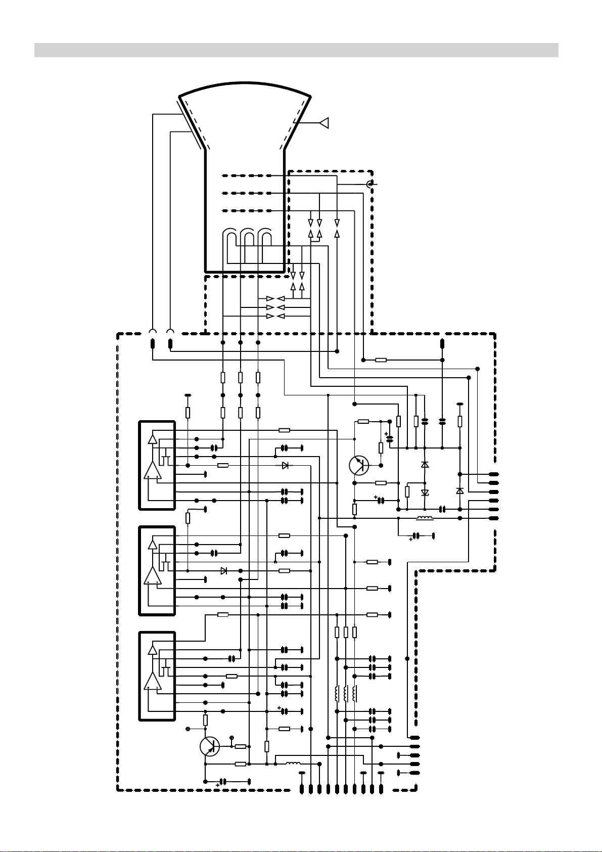
26
HH703/705 CRT-module
29k V
G 3 G 5
G 1 G 2
so1
R
G
6
8
CRT1
CRT2
470R
Rh22
Rh19
Rh21
Rh15
470k
987654321
TDA6 111
ICh3
54 87 93 62
1
TDA6 111
ICh2
2 63 97 84 51
TDA6 111
ICh1
th2
470R
Rh18
ch16
1n0
820R
Rh16
1M0
Rh10
1n0
ch11
LS41 48
Dh3
68k
Rh4
ch6
Rh3
820R
rh40
100R
1k0
rh39
BC85 7B
Ch28
100u
470R
rh38
f f
B
fgnd
9
11
470R
Rh24
470R
470R
Rh23
470R
1n0
rh1
68k
Rh17
22n
LS41 48
Dh4
22n
22nch12
Rh13
68k
22n
Ch9
22n
22n
ch3
22n
22n
Ch1
rh2
750R
2k2
Lh6
10u
10
4
Ch14
ch13
Rh12 820R
ch8
ch7
Ch4
ch2
ch5
47u
Xh2- 10
rh36
BF42 2
Th1
Rh26
rh6
1k5
rh7
22n
Lh3
68p
Lh2
2u2
FOCU S
CRT_ CONN
5
7
Rh33
1k5
1k5Rh28
100k
2k2
rh37
Ch27
10u
Rh27
4M7
rh41
10u
Ch18
33k
1k5
rh14
1k5
rh11
rh9
1k5
rh8
1k5
1k5
ch25
150p
ch24
150p
2u2
150p
ch23
68p
2u2
Lh4
Ch20
68p
ch15
68p
ch10
Xh2- 1
UG2
18k
220nCh21
Rh29
Dh1
BYW3 6C
0R0
Lh1
4u7
Ch17
22R
8n2
rh31
Ch22
Xh1- 6
Dh2
BYW3 6C
BZX8 4C15
dzh1
22n
Ch19
10u
Xh3- 1
Xh3- 5
Xh1- 1
Page 81
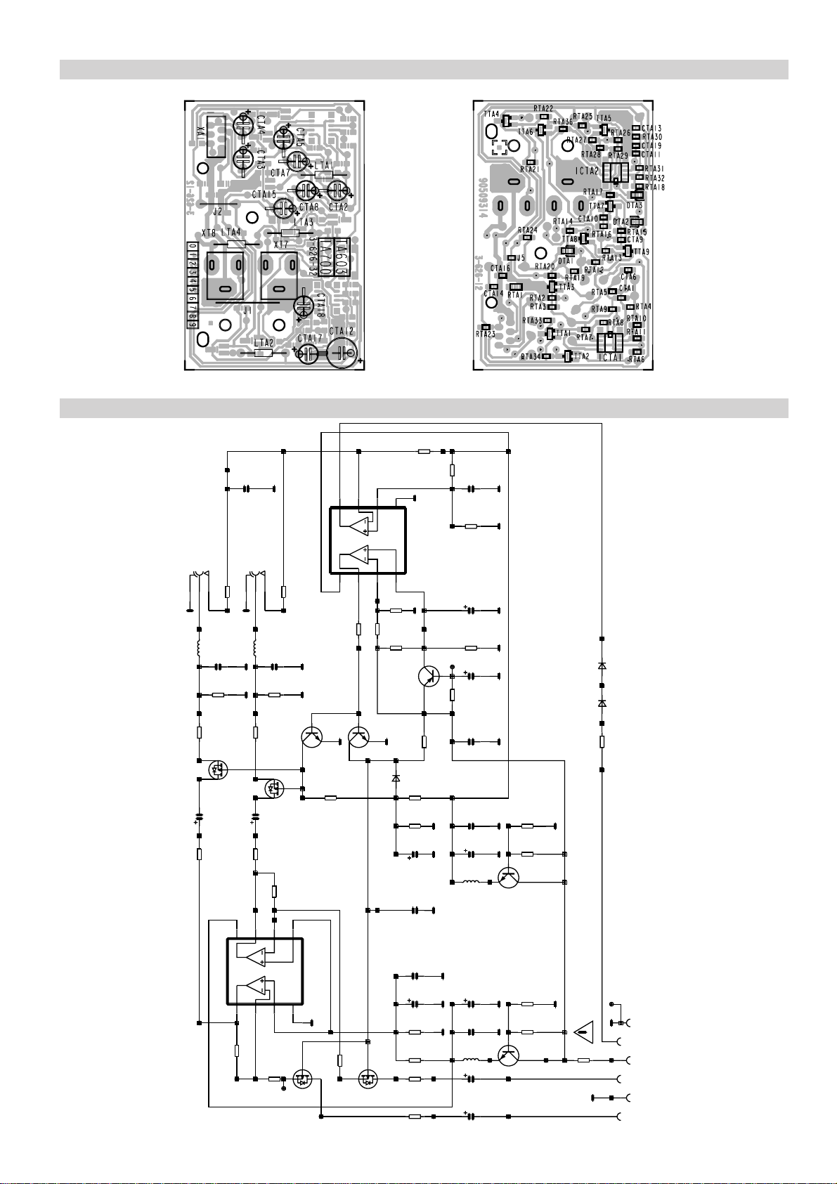
TA700 Audio output module
TA700 Audio output module
27
RCA
Xt7
1M0
DD
rta 1 7
10u
Lta 3
cta 9
10n
33k
rta 1 5
470 R
rta 1 3
tta 9
2N7 0 0 2
1u0
Cta 7
rta 9
100 R
8
680 k
D
2
18
100 n
cta 1 1
Xt8
RCA
1M0
rta 1 8
10u
Lta 4
cta 1 0
10n
D
D
470 R
rta 1 4
7
D
D
33k
rta 1 6
tta 7
BC8 4 7B
tta 8
Cta 8
1u0
100 R
rta 1 0
rta 1 1
6
rta 1 2
2N7 0 0 2
180 k
3
7
6
390 R
470 R
rta 2 8
rta 3 6
tta 6
BC8 4 7B
10k
rta 3 2
D
4
LM3 5 8
ict a 2
5
D
464 R
rta 2 9
12k 1
rta 2 7
tta 5
BC8 5 7B
D
LS4 1 4 8
220 k
dta 1
rta 2 0
220 k
rta 1 9
22u
Cta 1 5
470 p
cta 1 4
100 k
rta 3 1
D
100 n
cta 1 9
120 k
rta 3 0
22u
Cta 1 8
10k 0
rta 2 6
22u
D D D D
Cta 1 7
10k
rta 2 5
100 n
cta 1 6
100 k
rta 2 4
D
D
D
100 n
cta 1 3
100 u
Cta 1 2
10u
Lta 2
33k
rta 2 2
D
470 R
rta 2 1
tta 4
BC8 4 7 B
dta 3
LS4 1 4 8
dta 2
LS4 1 4 8
27k
rta 2 3
D
100n
cta6
Cta 2
47u
TL08 2 CD
1
2
180 k
rta 8
icta 1
3
4 5
tta1
2N7 0 0 2
rta 7
100 k
tta 2
100 k
rta 6
Cta 5
33k
rta 5
rta4
33k
2N70 0 2
10k
rta 3 4
10k
rta 3 3
10u
100 n
cta 1
10u
Lta1
22u
Cta 4
22u
Cta 3
33k
rta 3
rta 2
470 R
BC8 4 7 B
tta 3
D
Xa1 - 6
2R2
rta 1
Xa1 - 1
Page 82
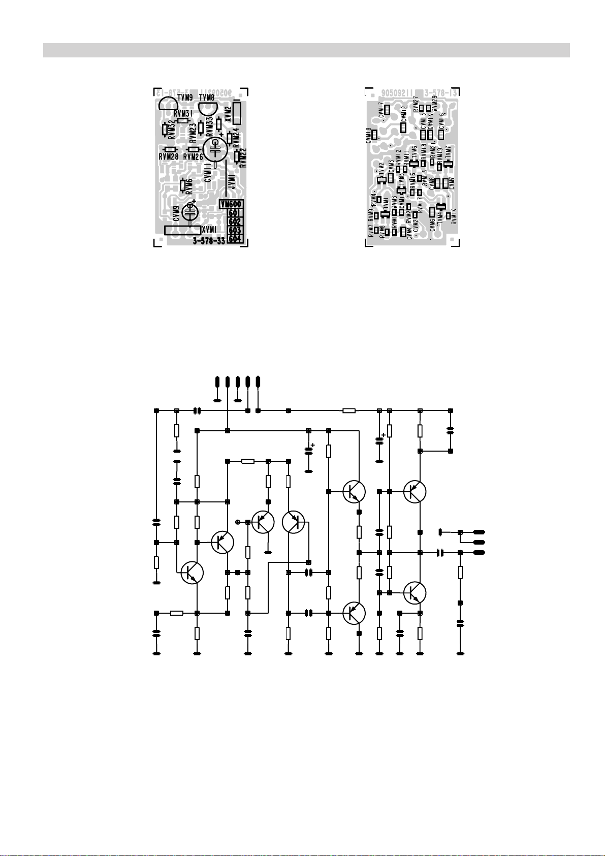
VM600 SVM-module
29
cv m 1
15 p
rvm 1
3k9
470 R
rvm 2
cvm 3
100 n
BF5 9 9
rvm 8
100 R
cv m 4
10n
rvm 3 10k
tvm 1
cv m 2
47p
Rv m 6
100 R
BF8 2 4
rvm 4 1 k0
rvm 7
680 R
Xvm 1 -1
tvm 2
rv m 9
820 R
cv m 6
10 0 n
rvm 1 3
1k0
rvm 1 6
47R
tv m 3
BF8 2 4
rvm 1 2
470 R
rvm 1 1
470 R
rvm 1 4
820 R
Cvm 9
10u
rvm1 7
47R
tvm 4
BF8 2 4
cvm 8
22n
cvm 7
22n
rvm 2 1
6k8
Rvm2 2
330R
rvm 1 8
6k8
tvm 6
BF5 9 9
Rvm 2 6
10R
Rvm 2 8
10R
rvm 1 9
560 R
tvm 7
BF8 2 4
Cvm 1 1
47u
cvm 1 3
cvm 1 4
Rvm 3 1
cvm 1 7
100n
Tvm 9
BC6 3 7
cvm 1 2
100 n
Xvm 2 -1
rvm 3 3
100 R
cvm 1 8
2n2
Rvm2 4
Rvm 2 3
100 R
BC63 8
100 n
rvm2 7
5k6
rvm 2 9
5k6
100 n
100R
Tvm 8
cvm 1 6
3R3
Rvm 3 2
3R3
100 n
Page 83
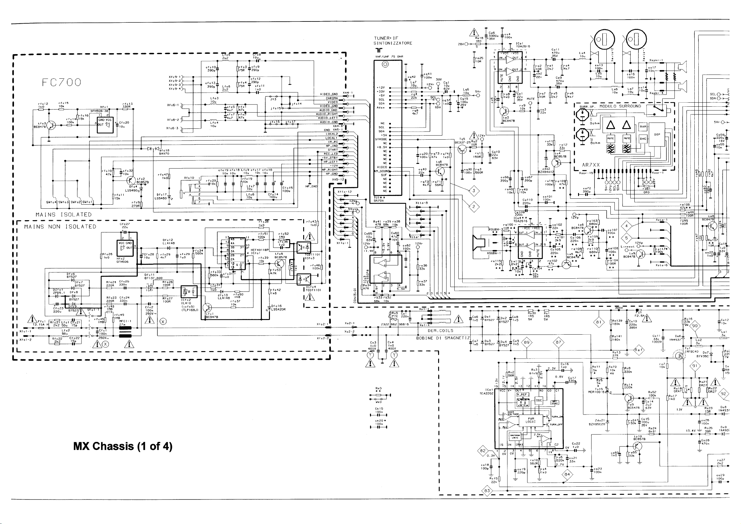
Page 84
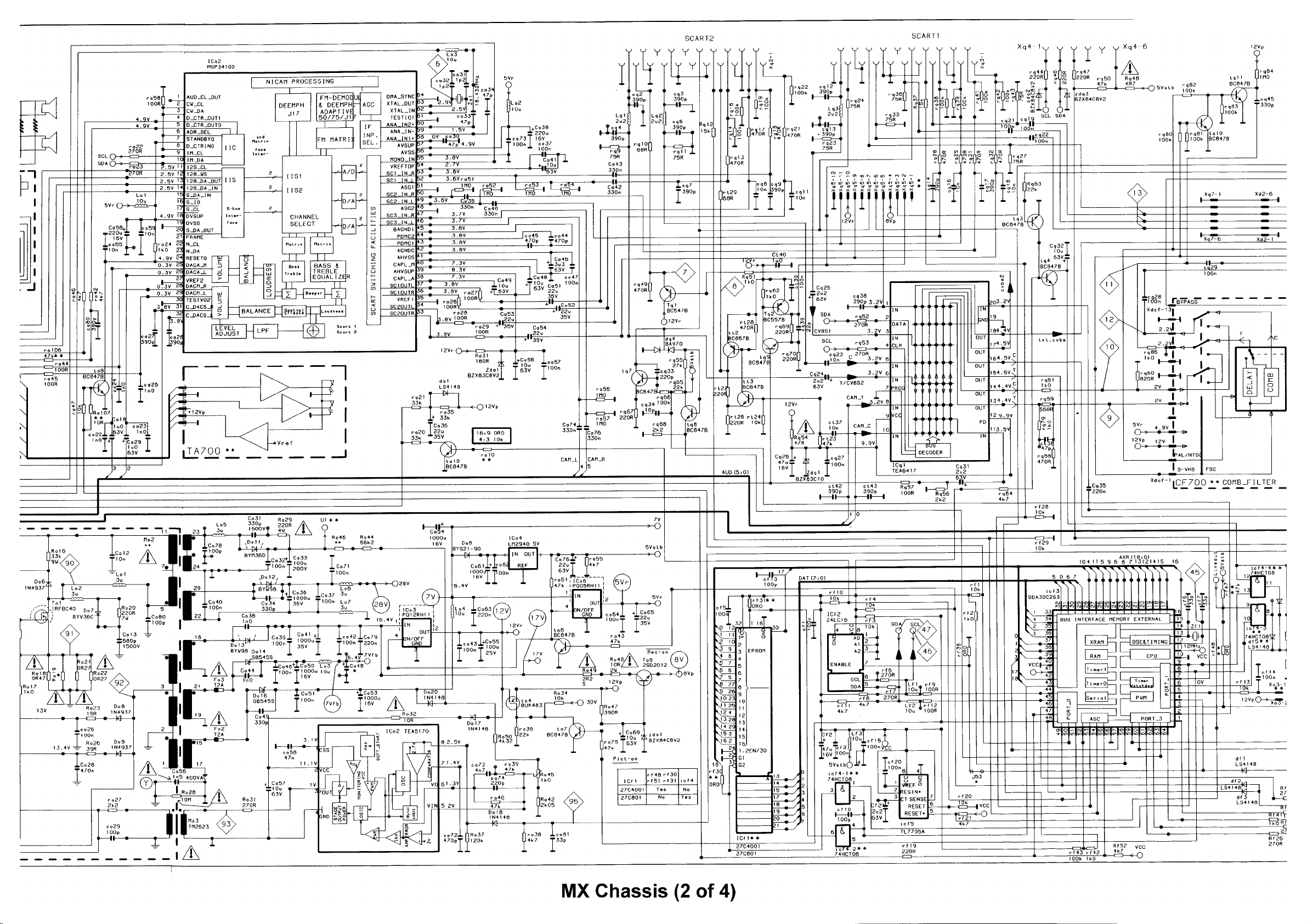
Page 85
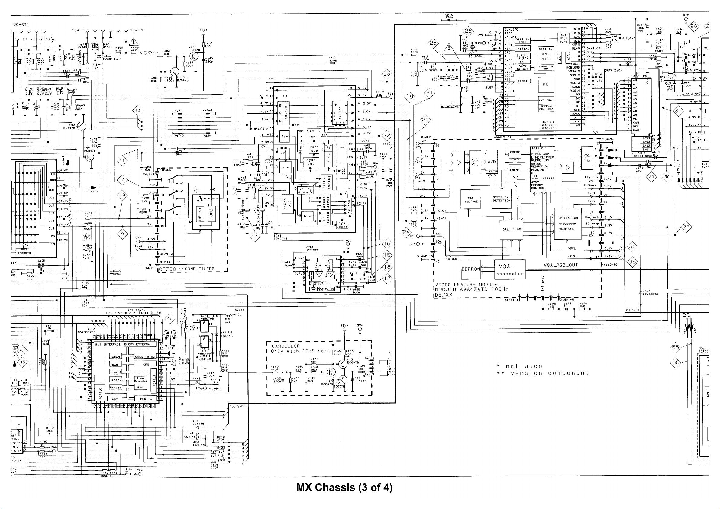
Page 86
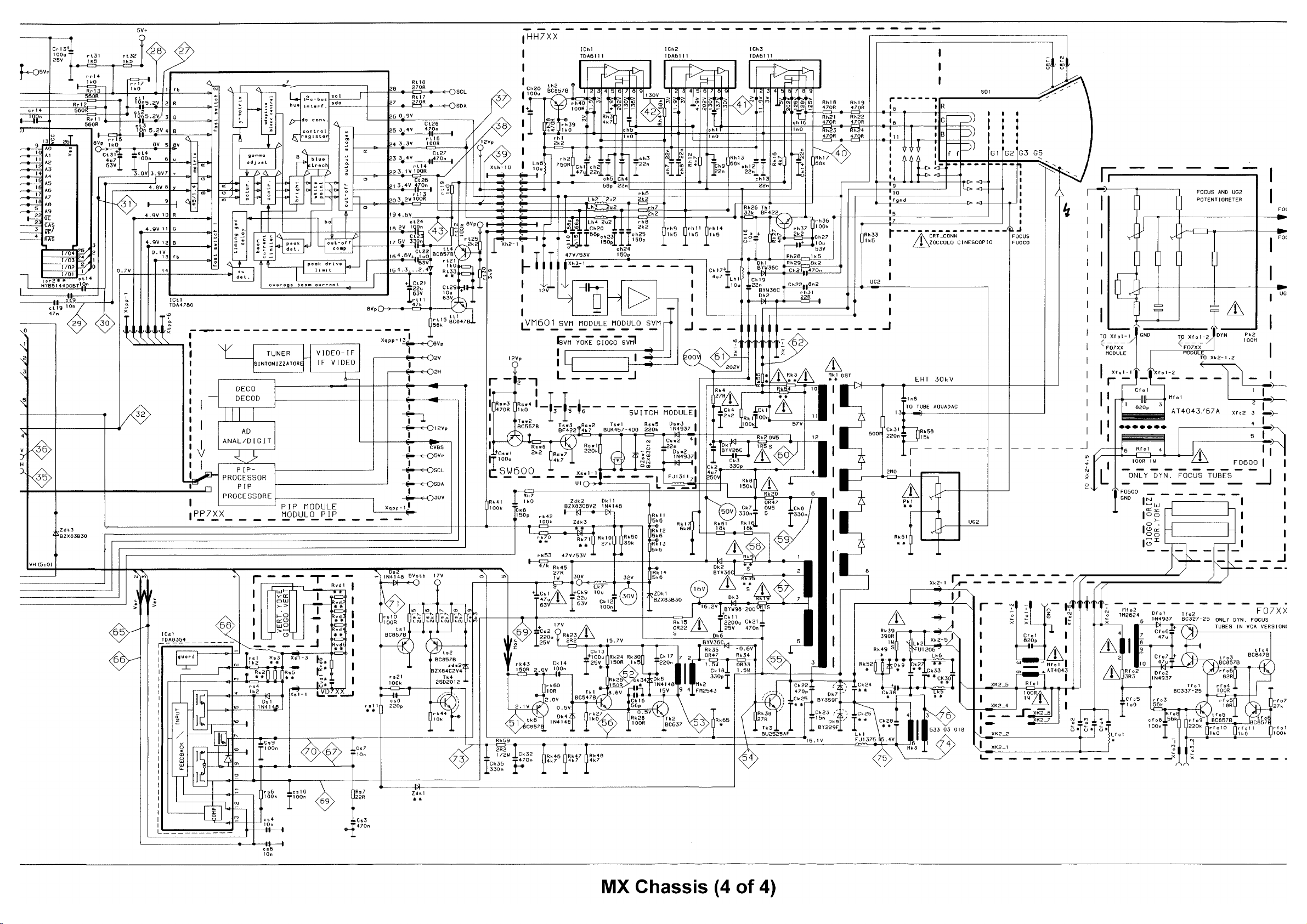
Page 87
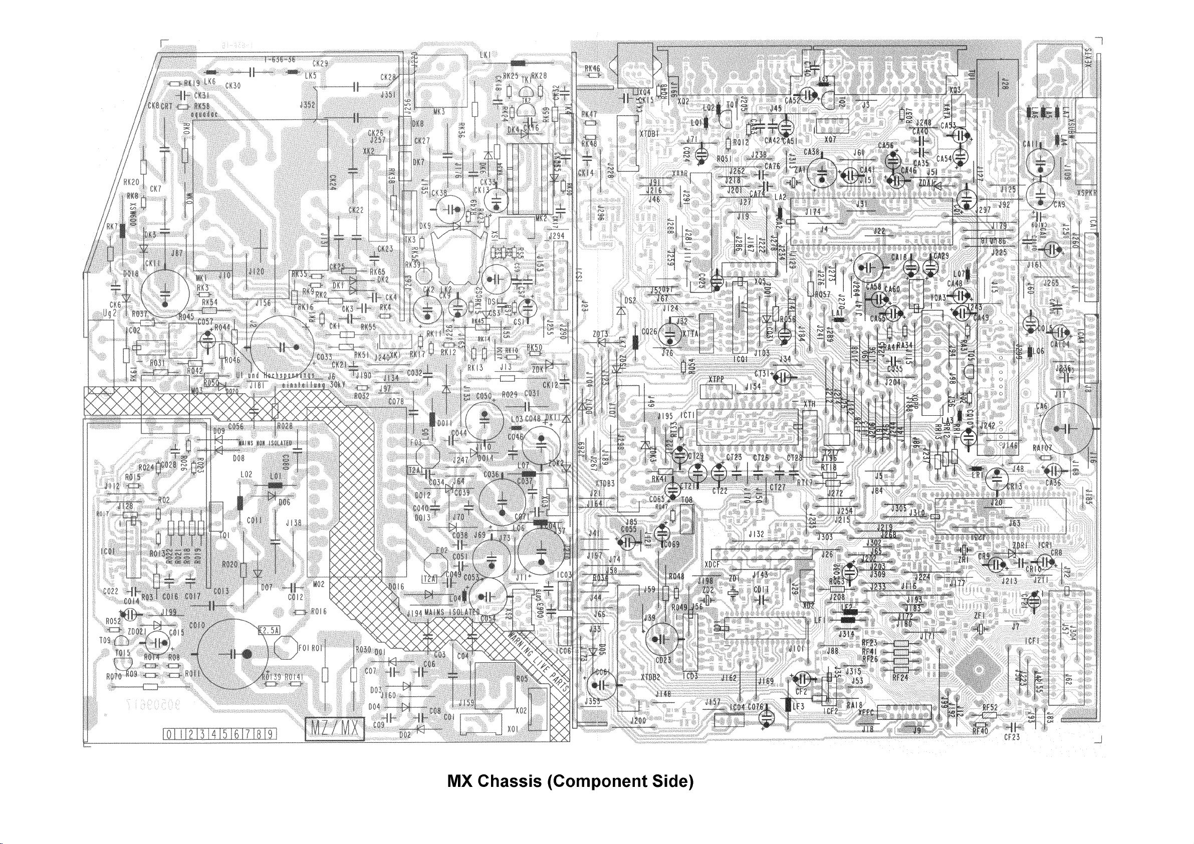
Page 88
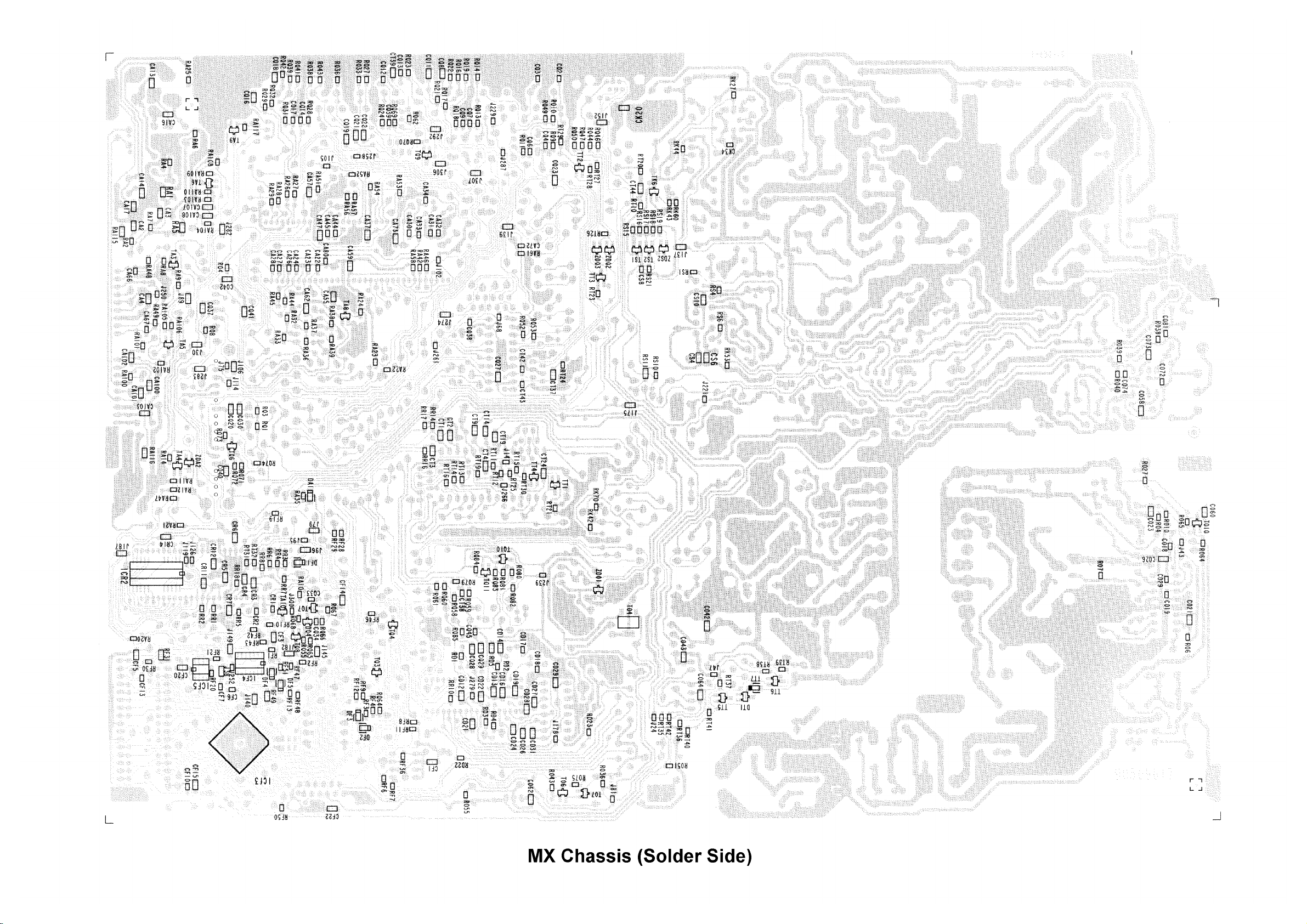
Page 89
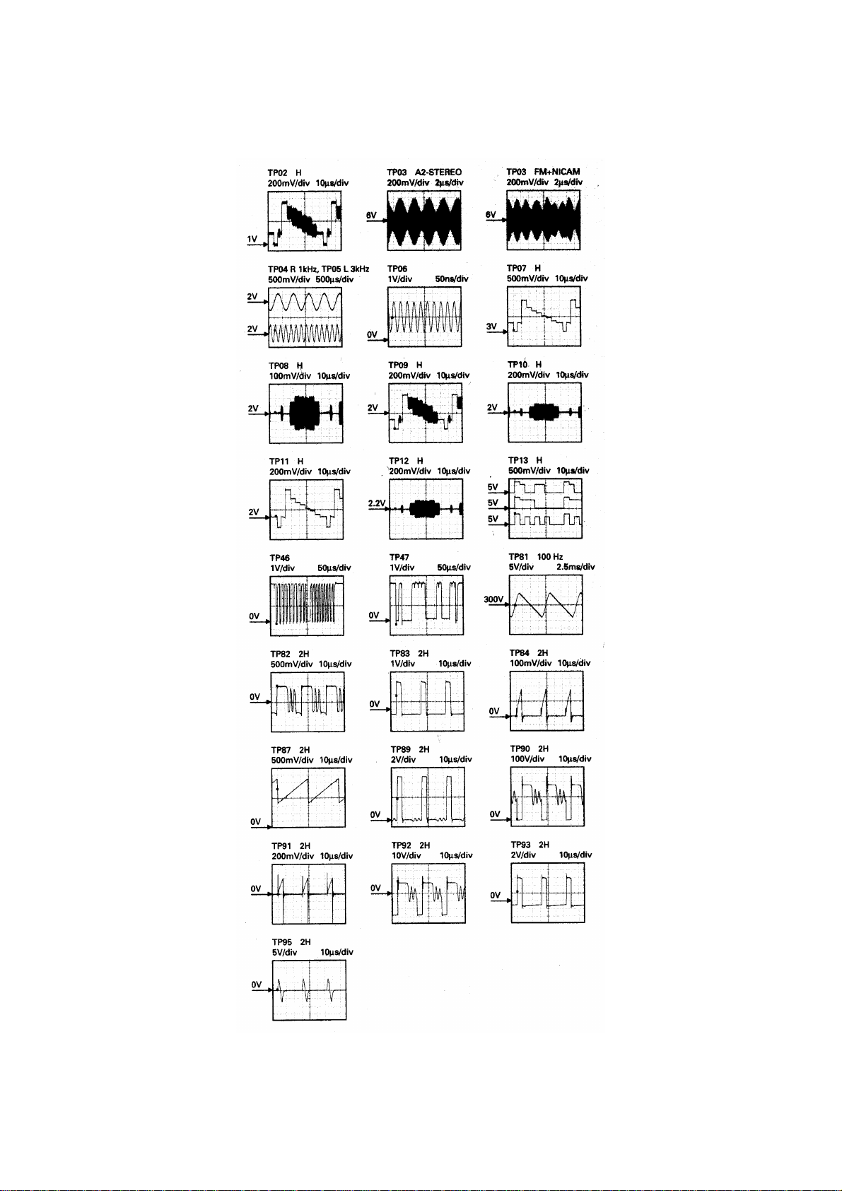
Page 90
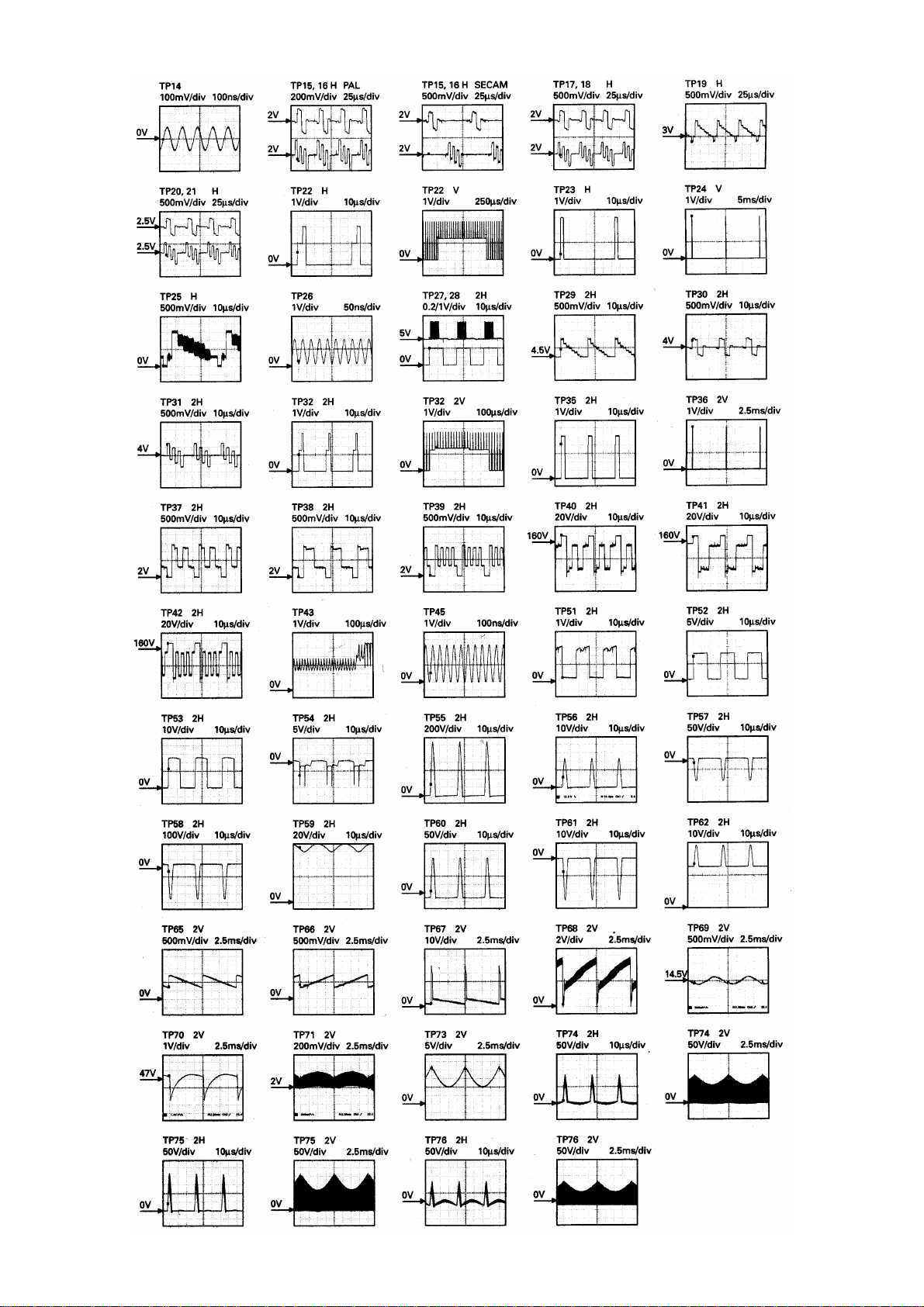
Page 91
30
G Variable components
D Röhrenabhängige Bauteile
F Composants variables
Picture Tube Vi 29 Phi 28
A68 EGD A66 EAK
038x322 552x44
Mainboard MX***C* MX***P*
PW-block PW700 PW719
Ck24 13n SAL3345 0046 11n SAL3345 0054
Ck25 680p SAL3345 0053
Ck26 33n SAL3346 0023 27n SAL3345 0063
Ck27 330n SAL3345 0034 390n SAL3345 0040
Ck28 4u7 SAL3366 0002 470n SAL3345 0041
Ck30 47n SAL3345 0036 120n SAL3324 1026
Rk3 4R7 SAL3186 0002 8R2 SAL3163 0090
Rk54 1R0 SAL3185 0001 8R2 SAL3163 0090
Rk55 1R0 SAL3181 0014 3R0 SAL3185 0007
Zdk3 15V SAL3677 0017 18V SAL4100 3183
Rs2 1R21 SAL3145 0008 1R1 SAL3145 0013
Rs3 1R21 SAL3145 0008 1R1 SAL3145 0013
Rs11 390k SAL3163 0092 680k SAL3154 8989
Zds1 15V SAL3677 0017 18V SAL4100 3183
Ro46 86k6 SAL3144 0051 100k SAL3144 0014
Lk6 47uH SAL4562 0035 jumper 5,0 SAL8570 0050
Mk1 1182.9001 SAL4536 0020 1182.9018 SAL4536 0036
CRT-module HH703 HH705
SW-module SW700 SW710
Vert.dump. VD707 VD710
Conn.wire SAL9601 0134
Xs2 No
U1 130V 140V
PWL No Yes
XO3 No
MO2 FM3604 SAL4532 0026 FM3605 SAL4532 0028
Page 92

Spare parts Ersatzteile Pièces de rechange
31
Note! Hinweis! Remarque !
w
Safety components in accordance with existing safety
regulations. These components must be replaced only
with original parts.
w
Sicherheitsbauteil im Sinn der Sicherheitsbestimmung.
Diese Teile dürfen nur durch Originalteile ersetzt werden.
w
Composant de sécurité conformément aux
règlementations de sécurité. Ces composants doivent
être uniquement remplacés par des pièces d'origines.
* Variable components
* Röhrenabhängige Bauteile
* Composants variables
Main board
28” Chassis MXEABP1 * SAL5863 1453
29” Chassis MXEABC2 * SAL5863 1415
Item Description Order no.
RESISTORS
RA 1, 5 RES 2,2 K 0,125W CHIP SAL3142 5625
RA 2, 7, 25 RES 10E 0,1W CHIP SAL3142 5810
RA 4, 6, 42, 46 RES 4,7K 0,1W CHIP SAL3142 5824
RA 8, 24 RES 1 K 0,1W CHIP SAL3142 5820
RA 9, 10, 32,
38, 47, 48, 49 RES 10K 0,1W CHIP SAL3142 5833
RA 11, 12, 20,
21, 35, 36, 37 RES 33K 0,1W CHIP SAL3142 5840
RA 14 RES 100K 0,1W CHIP SAL3142 5844
RA 18
RA 22, 23 RES 270 E 0,065W CHIP SAL3142 5855
RA 31 R CARF 180 5% 0W25 FP SAL3163 0026
RA 33, 39 R SMD 68K 5% 0W1 SAL3142 5838
RA 34, 41 R CARF 47R 5% 0W25 FP SAL3151 4525
RA 51, 52, 53,
RA 58, 44, 45,
RA 61 RES 0,0E 0,1W JUMPER SAL3142 5802
RD 1 RES 15K 0,1W CHIP SAL3142 5835
RD 2 R SMD 82K 5% 0W1 SAL3142 5843
RD 3, 4 RES 270 E 0,065W CHIP SAL3142 5855
RD 22, 23 RES 1 K 0,1W CHIP SAL3142 5820
RF 1, 3, 4, 10,
RF 2, 42 RES 1 K 0,1W CHIP SAL3142 5820
RF 6, 7 RES 270 E 0,065W CHIP SAL3142 5855
RF 8, 11, 21 RES 4,7K 0,1W CHIP SAL3142 5824
RF 9, 12 RES 100E 0,1W CHIP SAL3142 5852
RF 19 RES 220E 0,1W SMD SAL3142 5815
RF 30, 36, 48, 51 RES 0,0E 0,1W JUMPER SAL3142 5802
RF 31 WID 0 E 0,125W CHIP JUMP SAL3142 5601
RF 23, 41 R CARF 1K0 5% 0W25 SAL3166 0016
RF 24, 26 R CARF 270R 5% 0W25 SAL3166 0011
RF 40 RES 270R0,25W FP SAL3163 0027
RF 43 RES 100K 0,1W CHIP SAL3142 5844
RF 52 R CARF 4K7 5% 0W25 SAL3166 0031
RK 1 RES FUS 100K 1/4W SAL3163 0037
RK 2
RK 3 w* R FUS V 4R7 5% 0W25 SAL3186 0002
RK 3 w*, 54 w*RES 8R2 0W25 FP SAL3163 0090
RK 4
RK 7 R CARF 1K0 5% 0W25 SAL3166 0016
RK 8 R CF RD 150K J 1/4W SAL3163 0038
RK 9 w, 19 wR FUS I 0R1 10% 0W4 SAL3182 0003
RK 10 R CF RD 27K J 1/4W SAL3163 0035
RK 11, 12, 13, 14 R CF RD 5K6 J 1/4W SAL3163 0028
w
54, 56, 57 RES 1M 0,1W CHIP SAL3142 5801
26, 27, 28, 29 RES 100E 0,1W CHIP SAL3142 5852
13, 20, 28, 29 RES 10K 0,1W CHIP SAL3142 5833
w
w
RES 1 R 4W SAL3143 0013
WID 1R5 5% OW5 FP SAL3163 0014
SRES 27 E 0,25W SAL3186 0001
R
Item Description Order no.
RK 15
RK 16, 51 R CARF 18K 5% 0W25 SAL3166 0040
RK 17 R CF RD 6K8 J 1/4W SAL3163 0029
RK 20
RK 23
RK 24, 25 R CARF 150R 5% 0W25 FP SAL3163 0025
RK 27 RES 1 K 0,1W CHIP SAL3142 5820
RK 28 SRES 100E 0,25W SAL3151 4516
RK 30 RES 1K5 0,25W SAL3166 0017
RK 30 FUSE RES 1,5K 0,25W SAL3151 4523
RK 34 RES 0,33E 1,5W AX METOX SAL3143 0010
RK 36 RES 0,47E 1,5W AX METOX SAL3143 0011
RK 38 R CARF 27R 5% 0W25 SAL3166 0007
RK 39
RK 41 R CARF 100K 5% 0W25 SAL3166 0030
RK 42 RES 100K 0,1W CHIP SAL3142 5844
RK 43 RES 150E 0,1W CHIP SAL3142 5812
RK 44, 70 RES 10K 0,1W CHIP SAL3142 5833
RK 45
RK 46, 47, 48 SWID 4,7K 0,25W SAL3151 4522
RK 50 WID 39K 5% 0,25W SAL3163 0048
RK 53 RES 47K 0,1W CHIP SAL3142 5836
RK 54 w* R FUS V 1R0 5% 0W5 SAL3185 0001
RK 55 w* SWID 3,0 E 0W50 SAL3185 0007
RK 55 w* SRES 1 R 0,7W SAL3181 0014
RK 58 R CF RD 15K J 1/4W SAL3163 0033
RK 59 SRES 2R2 0W5 SAL3185 0056
RK 60 RES 10E 0,1W CHIP SAL3142 5810
RK 70 R CARF 10K 5% 0W25 FP SAL3163 0031
RO 1, 30 R WRLAC 1E5 5% 5W0 SAL3136 0004
RO 2 R CARF 56E 5% 0W25 FP SAL3163 0046
RO 3 R METF 61K9 1% 0W6 SAL3144 0013
RO 4 R SMD 1K00 1% 0W1 SAL3149 0056
RO 5 R PTC RS=24OHM FOR DEGA SAL3194 0001
RO 6 RES 220K 0,1W CHIP SAL3142 5847
RO 7, 39 RES 10K 0,1W CHIP SAL3142 5833
RO 8, 14 RES 330K 0,25W 5% FP SAL3151 8658
RO 10 R SMD 562R F 0W10 SAL3149 0081
RO 13 CARBON RE 27R 5% 0,25W F SAL3163 0021
RO 15 WID 22K 5% 0W25 SAL3163 0034
RO 16 R WRLAC 33K 10% 9W0 SAL3135 0002
RO 17 R CARF 1K0 5% 0W25 SAL3166 0016
RO 18
RO 20 RES 220R 7W SAL3135 0013
RO 21 w, 22 wR METF 0R27 5% 0W6 SAL3144 0029
RO 23 R CARF 15R 5% 0W25 FP SAL3163 0020
RO 24 RES 6,81K 0,6 W F METF SAL3145 0015
RO 26 R CARF 39R 5% 0W25 FP SAL3163 0023
RO 27 RES 2,2K 0,1W CHIP SAL3142 5828
RO 28
RO 29
RO 31 R CARF 270R 5% 0W25 SAL3166 0011
RO 32
RO 34 0W25 C F RES 10K 5% SAL3166 0022
RO 36 RES 22K 0,1W CHIP SAL3142 5837
RO 37 R METF 120K 1% 0W6 SAL3144 0016
RO 38, 55 RES 4,7K 0,1W CHIP SAL3142 5824
RO 39, 43, 51, 75 RES 47K 0,1W CHIP SAL3142 5836
RO 42 R METF 2K05 1% 0W6 SAL3144 0020
RO 44 RES 56,2K 0,6 W 1% SAL3144 0033
RO 45 R TRIM HOR 1K0 20% 0W1 SAL3123 0005
RO 46 * R METF 100K 1% 0W6 SAL3144 0014
RO 46 * R METF 86K6 F 0W60 SAL3144 0051
RO 47 R CARF 390R 5% 0W25 FP SAL3163 0041
RO 48
RO 49
RO 50 R METF 4K32 1% 0W6 SAL3144 0026
RO 52 RES FUS 100K 1/4W SAL3163 0037
RO 64 RES 150K 0,1W CHIP SAL3142 5846
RO 65 RES 33K 0,1W CHIP SAL3142 5840
RO 70 RES 10K 4W0 METOX SAL3144 0060
w
w
w
w
w
w
w
w
w
w
w
S RES 022E 0,25W SAL3151 4506
R FUS V 0R47 5% 0W5 SAL3185 0004
SRES 2,2E 0,25W SAL3151 4511
R FUS V 390R 10% 1W0 SAL3185 0002
R FUS V 27E K 1W0 SAL3184 0003
WID 0,47 0,6 W SAL3144 0019
R COMP HV 10M 5% 0W5 SAL3146 0001
R METOX 220R 5% 4W0 SAL3143 0004
S RES 10 E 0,25W SAL3151 4513
R METOX 10R 5% 2W0 SAL3143 0001
R FUS V 2R2 5% 0W25 SAL3186 0003
Page 93

32
Item Description Order no. Item Description Order no.
RO 139, 141 R CF RD 180K J 1/4W SAL3163 0039
RQ 1 RES 150E 0,1W CHIP SAL3142 5812
RQ 2
w
RQ 3, 59 RES 560 E CHIP SAL3142 5818
RQ 4, 65 RES 22K 0,1W CHIP SAL3142 5837
RQ 8, 64, 72 RES 4,7K 0,1W CHIP SAL3142 5824
RQ 9, 11, 43, 33,
36, 23, 24, 27 RES 75E 0,1W CHIP SAL3142 5861
RQ 10 RES 68E 5% CHIP SAL3142 5876
RQ 12, 37 R CF RD 15K J 1/4W SAL3163 0033
RQ 13, 21, 17,
18, 49, 58,
28, 29, 31, 32 RES 470 E 0,1W SMD SAL3142 5817
RQ 19, 22, 14,
16, 66, 38,
39, 41, 42,
80, 81, 82, 83 RES 100K 0,1W CHIP SAL3142 5844
RQ 48
RQ 50, 73 RES 47K 0,1W CHIP SAL3142 5836
RQ 51 SRES 1 K 0,25WW SAL3151 4519
RQ 52, 53 RES 270 E 0,065W CHIP SAL3142 5855
RQ 54
RQ 55 RES 27K 0,1 W CHIP SAL3142 5839
RQ 56 R CARF 2K2 5% 0W25 SAL3166 0037
RQ 57 R CARF AX 100R 0W25 AMMO SAL3166 0049
RQ 60 RES 820E 0,1W CHIP SAL3142 5819
RQ 63 R CARF 22K 5% 0W25 SAL3166 0025
RQ 67, 44, 46,
RQ 68 RES 2,2K 0,1W CHIP SAL3142 5828
RQ 71 RES 56E 5% CHIP SAL3142 5865
RQ 84 RES 1M 0,1W CHIP SAL3142 5801
RQ 85, 61,
RR 1 RES 10K 0,1W CHIP SAL3142 5833
RR 2, 14, 16, 17 RES 1 K 0,1W CHIP SAL3142 5820
RR 5 RES 100E 0,1W CHIP SAL3142 5852
RR 6, 3, 4 RES 3,9K 0,1W CHIP SAL3142 5830
RR 7 RES 470 E 0,1W SMD SAL3142 5817
RR 8 RES 4,7K 0,1W CHIP SAL3142 5824
RR 10 RES 33K 0,1W CHIP SAL3142 5840
RR 11, 12, 13 RES 560R 0W25 SAL3166 0050
RR 18 RES 0,0E 0,1W JUMPER SAL3142 5802
RS 1, 4 RES 1,2K 0,125W SAL3142 5822
RS 2 *, 3 * R METF 1R21 1% 0W6 SAL3145 0008
RS 2 *, 3 *, 5 R METF 1R10 F 0W60 SAL3145 0013
RS 6 R SMD 180K 5% 0W1 SAL3149 0012
RS 7 SWID 22 E 0,25 W SAL3151 4527
RS 10 RES 100E 0,1W CHIP SAL3142 5852
RS 11 * R SMD 680K 5% 0W1 SAL3149 0059
RS 11 * RES 390K 0,25W SAL3163 0092
RS 15, 16, 17, 18 RES 2,7K 0,125W SAL3142 5821
RS 19 RES 3,3K 0,1W CHIP SAL3142 5829
RS 21 RES 100K 0,1W CHIP SAL3142 5844
RT 10, 19, 20, 21 RES 1 K 0,1W CHIP SAL3142 5820
RT 11, 23 RES 47K 0,1W CHIP SAL3142 5836
RT 12 RES 100K 0,1W CHIP SAL3142 5844
RT 15 RES 56K 0,1W CHIP SAL3142 5842
RT 16, 13, 14 RES 100E 0,1W CHIP SAL3142 5852
RT 17, 18 R CARF 270R 5% 0W25 SAL3166 0011
RT 24 RES 10K 0,1W CHIP SAL3142 5833
RT 25 RES 2,2K 0,1W CHIP SAL3142 5828
RT 28 RES 470 E 0,1W SMD SAL3142 5817
RT 29 RES 68E 5% CHIP SAL3142 5876
RT 30 RES 3,9K 0,1W CHIP SAL3142 5830
RT 33 * R CF RD 560R J 1/4W SAL3163 0047
RT 33 * RES 1K2 0,25W FP SAL3151 8510
RT 26, 27 RES 220E 0,1W SMD SAL3142 5815
RT 31, 32 RES 1,5 K 5% SMD SAL3142 5826
w
w
47, 69, 70 RES 220E 0,1W SMD SAL3142 5815
62, 74, 79 RES 1 K 0,1W CHIP SAL3142 5820
S RES 10 E 0,25W SAL3151 4513
R FUS V 4R7 5% 0W25 SAL3186 0002
R CARF 47R 5% 0W25 FP SAL3151 4525
CAPACITORS
CA 1, 36, 51,
52, 53, 54 C ELYT 22U 20% 35V SAL3454 0021
CA 2, 3 C CER SMD 22N 10% 50V SAL3253 5914
CA 4, 5, 13,
16, 37, 47, 57,
62, 73, 101 CAP 100NF 50V CER SAL3253 5920
CA 6 C ELYT 3300U 20% 35V SAL3451 0009
CA 9, 11 ECAP 470MF 35 V SAL3422 0648
CA 14, 17, 55, 59 CAP 10NF 50V CHIP SAL3253 5918
CA 18, 29 EL, CAP, 1UF 63V SAL3454 0022
CA 22, 23, 24, 26 CAP 1NF 50V SAL3253 6203
CA 27, 28, 80,
66, 67, 72 C CER SMD 390P 5% 50V SAL3219 0012
CA 30, 33, 34 CAP 47PF 50V CHIP SAL3212 5508
CA 31, 32 C CER SMD 1P2 5% 50V SAL3218 0008
CA 35, 40, 42,
43, 74, 76 POLYESTER 330N 63V PAN 2 SAL3312 7113
CA 38, 58 EL,CAP, 220UF 16V 13X17 SAL3451 0003
CA 41, 56,
65, 48, 49 C ELYT 10U 20% 63V SAL3454 0025
CA 44, 45 C CER SMD 470P 5% 50V SAL3219 0013
CA 46 C ELYT 3U3 20% 63V SAL3454 0029
CA 60 C ELYT 47U 20% 16V SAL3454 0019
CA 109, 110 C MKT 220N 10% 63V SAL3312 7108
CD 11 POLYESTER 470N 10% 63V SAL3312 7123
CD 12, 16 C CER SMD 3N3 10% 50V SAL3253 5908
CD 13, 14, 19,
21, 22, 24, 26,
27, 28, 29, 31 CAP 100NF 50V CER SAL3253 5920
CD 17, 18 CAP 18 PF 50V CHIP SAL3212 5520
CD 23 C EL RD 100U M 25V SAL3454 0020
CF 1, 3, 5,
14, 15, 20 CAP 100NF 50V CER SAL3253 5920
CF 2 C ELYT 47U 20% 16V SAL3454 0019
CF 6, 7 CAP 33PF 50V CHIP SAL3212 5507
CF 10, 13 CAP 100PF 50V SAL3212 5515
CF 21 C ELYT 2U2 20% 63V SAL3454 0023
CK 1 C MKT 100N 10% 250V SAL3336 0003
CK 2 C ELYT 4U7 250V 11x13 HV SAL3461 0001
CK 3, 18 C CER 330P 10% 500V SAL3278 0002
CK 4 C CER 2N2 20% 500V SAL3278 0003
CK 6 C CER 150P 10% 500V SAL3278 0001
CK 7, 8 C MKC 330N 10% 250V SAL3366 0001
CK 9 EL, CAP, 22U 63V PAR SAL3454 0026
CK 11 C ELYT 2200U 20% 25V SAL3451 0005
CK 12, 14, 15 POLYESTER 100n 10% 63V SAL3312 7106
CK 13 C EL RD 100U M 25V SAL3454 0020
CK 16 C CER 56P 5% 50V SAL3218 0001
CK 17, 31 C MKT 220N 10% 63V SAL3312 7108
CK 21, 32 POLYESTER 470N 10% 63V SAL3312 7123
CK 22 C MKP 470P 2,5% 1K6V SAL3346 0011
CK 23 C (M)KP 15N 2,5% 100V SAL3346 0003
CK 24 * CAP 13NF SAL3345 0046
CK 24 * CAP 11NF SAL3345 0054
CK 25 * CAP 680PF SAL3345 0053
CK 26 * COND 15NF 2,5% 630V SAL3346 0023
CK 27 * C MKP 330N J 250V SAL3345 0034
CK 27 * C 390NF 250V SAL3345 0040
CK 28 * C MKC 4U7 10% 63V SAL3366 0002
CK 28 * C 470NF 250V SAL3345 0041
CK 30 * C MKP 47N 3,5% 400V SAL3345 0036
CK 30 * SCAP 0,12MF400V SAL3324 1026
CK 36 POLYESTER 330N 63V PAN 2 SAL3312 7113
CO 1 C MKT 220N 10% 400V SAL3336 0002
CO 3 w, 4
CO 6, 7, 8, 9 SCAP 1,5 NF 2KV SAL3267 0976
CO 10 C ELYT 220U 20% 385V SAL3426 0826
CO 11 C MKP 33N 5% 1KV SAL3346 0016
CO 12 C MKT 10N 5% 400V SAL3336 0006
CO 13 CAP 680PF SAL3345 0053
CO 14 C ELYT 2U2 20% 63V SAL3454 0023
CO 15 EL,CAP, 100u 35V 13x21 R SAL3451 0006
CO 16 KON 1NO 5% 63V SAL3348 0010
w
SCAP 1 NF 4KV SAL3261 0931
K
Page 94

Item Description Order no. Item Description Order no.
CO 17 POLYESTER 330N 63V PAN 2 SAL3312 7113
CO 18, 29 CAP 100PF 50V SAL3212 5515
CO 19, 74 CAP 220 PF 50V SAL3212 5513
CO 21 C CER SMD 33N 20% 50V SAL3279 0010
CO 22 C MKT 1U0 10% 63V SAL3312 4758
CO 23, 26, 62,
64, 42, 43 CAP 100NF 50V CER SAL3253 5920
CO 28 POLYESTER 470N 10% 63V SAL3312 7123
CO 31 C (M)KP 330P 10% 1K6V SAL3346 0017
CO 32 C MKT 100N 10% 250V SAL3336 0003
CO 33 C ELYT 100U 20% 200V SAL3461 0006
CO 34, 38, 44 C CER 1N0 10% 500V SAL3278 0004
CO 34, 49 C CER 330P 10% 500V SAL3278 0002
CO 36, 41 C ELYT 1000U 20% 35V SAL3451 0013
CO 37, 46, 51,
71, 39, 40 POLYESTER 100n 10% 63V SAL3312 7106
CO 50, 61, 53, 54 C ELYT 1000U 20% 16V SAL3451 0004
CO 55 C EL RD 100U M 25V SAL3454 0020
CO 56
CO 57, 69 C ELYT 10U 20% 63V SAL3454 0025
CO 58 C CER SMD 47N 10% 50V SAL3279 0008
CO 60 CAP 1NF 50V SAL3253 6203
CO 63, 79 C MKT 220N 10% 63V SAL3312 7108
CO 65 C ELYT 22U 20% 35V SAL3454 0021
CO 72 C CER SMD 470P 5% 50V SAL3219 0013
CO 73 C CER SMD 4N7 10% 50V SAL3279 0007
CO 76 EL, CAP, 22U 63V PAR SAL3454 0026
CO 81 CAP 33PF 50V CHIP SAL3212 5507
CQ 1, 32 C ELYT 10U 20% 63V SAL3454 0025
CQ 8, 11,
CQ 9, 17, 2,
CQ 10 EL, CAP, 22U 63V PAR SAL3454 0026
CQ 15 C EL RD 100U M 25V SAL3454 0020
CQ 26 C ELYT 47U 20% 16V SAL3454 0019
CQ 31, 24, 25 C ELYT 2U2 20% 63V SAL3454 0023
CQ 33 CAP 220 PF 50V SAL3212 5513
CQ 34 CAP 10PF 50V SMD SAL3212 5506
CQ 35 C MKT 220N 10% 63V SAL3312 7108
CQ 37 CAP 1 NF 50V CHIP SAL3253 5901
CQ 39 CAP 22PF 50V SAL3212 5521
CQ 40 C CER SMD 22N 10% 50V SAL3253 5914
CQ 41, 19, 20,
CQ 45 CAP 330PF 50V SAL3212 5517
CR 1, 2 CAP 33PF 50V CHIP SAL3212 5507
CR 8 C ELYT 10U 20% 63V SAL3454 0025
CR 9 C ELYT 22U 20% 35V SAL3454 0021
CR 10 POLYESTER 470N 10% 63V SAL3312 7123
CR 13 C EL RD 100U M 25V SAL3454 0020
CR 14, 11, 12,
CS 1 C ELYT 47UF M 63V SAL3454 0053
CS 2 ECAP 220MF 25V SAL3422 9784
CS 3 POLYESTER 470N 10% 63V SAL3312 7123
CS 4, 6 CAP 10 NF 50V CHIP SAL3253 6213
CS 7 CAP 10N 250V SAL3345 0057
CS 8 CAP 220 PF 50V SAL3212 5513
CS 9 POLYESTER 100n 10% 63V SAL3312 7106
CS 10 CAP 100NF 50V CER SAL3253 5920
CT 1, 2, 3,
CT 4, 24, 39 CAP 100NF 50V CER SAL3253 5920
CT 19 C CER SMD 47N 10% 50V SAL3279 0008
CT 21 EL, CAP, 22U 63V PAR SAL3454 0026
CT 22 EL, CAP, 1UF 63V SAL3454 0022
CT 23 POLYESTER 330N 63V PAN 2 SAL3312 7113
CT 26, 27, 28 POLYESTER 470N 10% 63V SAL3312 7123
CT 29 C ELYT 10U 20% 63V SAL3454 0025
CT 31 C ELYT 4U7 20% 63V SAL3454 0024
CT 38 CAP 47PF 50V CHIP SAL3212 5508
CT 40 C MKT 1U0 10% 63V SAL3312 4758
CT 42, 43 C CER SMD 390P 5% 50V SAL3219 0012
w
16, 18, 23 CAP 10NF 50V CHIP SAL3253 5918
3, 4, 6, 7,
38, 12, 13, 14 C CER SMD 390P 5% 50V SAL3219 0012
21, 22, 27,
28, 29, 30 CAP 100NF 50V CER SAL3253 5920
3, 4, 5, 6, 7 CAP 100NF 50V CER SAL3253 5920
9, 14, 37, 44 CAP 10NF 50V CHIP SAL3253 5918
C CER 1N5 20% 400VAC SAL3296 0002
TRANSISTORS
TA 3, 8, 9, 10 TRANS BC 847B SAL3614 5312
TA 4 TRANS BC 857B CHI SAL3614 5412
TK 1 TRANS BC 547B 45V 10 SAL3622 0002
TK 2 TRANS BC637 60V 1a SAL3622 0003
TK 3 TRANS BU2525AF 1K5V SAL3627 0003
TK 3 CLIP SAL8681 7341
TK 4 TRANS 2SD2012 60v SAL3627 0004
TK 4 FASTENING SPRING DN74009 SAL7358 4994
TK 6 TRANS BC 857B CHI SAL3614 5412
TO 1 CLIP SAL8681 7341
TO 1 TRANS IRFBC40 600V SAL3637 0001
TO 1 ISOLATOR TO-220 SAL8231 8802
TO 4 TRANS BUK483 60A 60V SAL3638 0001
TO 6, 7 TRANS BC 847B SAL3614 5312
TO 8 TRANS 2SD2012 60v SAL3627 0004
TO 9 TRANS BC 547B 45V 10 SAL3622 0002
TO 10 TRANS BC 857B CHI SAL3614 5412
TO 15 THYRISTOR MCR100-6 400V SAL3610 0001
TQ 1 TRANS BC 547B 45V 10 SAL3622 0002
TQ 2 TRANS BC 557B SAL3614 6424
TQ 3, 4, 6, 7,
8, 9, 10, 11 TRANS BC 847B SAL3614 5312
TQ 5 TRANS BC 337-25 SAL3614 7138
TS 1, 2 TRANS BC 858C SAL3614 5423
TT 1, 3 TRANS BC 847B SAL3614 5312
TT 2, 4 TRANS BC 857B CHI SAL3614 5412
DIODES
DA 1 DI SMD LS4148 75V 200MA SAL3649 0002
DF 1, 2, 3 DI SMD LS4148 75V 200MA SAL3649 0002
DK 1 DIODE BYV26C 600V 1 SAL3661 0005
DK 2, 6 DIODE BYV36C 600V 1 SAL3657 5452
DK 3 DIODE BYW 98-200 SAL3657 5470
DK 4, 5, 11 DI 1N4148 75V 200MA DO35 SAL3642 0002
DK 7 DIODE BY359F 1K5V 5 SAL3657 1465
DK 8 DIODE BY229F 800V 7 SAL3661 0004
DK 7, 8 CLIP SAL8681 7341
DO 5 DIODE BYS21-90V 1,0A SAL3662 1556
DO 7 DIODE BYV36C 600V 1 SAL3657 5452
DO 1, 2, 3, 4 DIODE BY527 1K25V 2 SAL3661 0001
DO 6, 8, 9 DIODE 1N4937 SAL3657 5353
DO 11 DI RECT BYM36D 800V 2,9A SAL3662 1551
DO 12, 13 DIODE BYW 98-200 SAL3657 5470
DO 14, 16 DIODE SB545S 45V 5A SAL3642 0003
DO 17, 18, 20 DI 1N4148 75V 200MA DO35 SAL3642 0002
DQ 4 DIODE BAV 70 SMD SAL3656 1954
DS 1, 2 DI 1N4148 75V 200MA DO35 SAL3642 0002
ZENERS
ZDA 1 Z DI BZX83B 8V2 2% DO35 SAL3677 0009
ZDA 2 ZDIODE BZX84A 12V 1% SAL3677 0019
ZDK 1 DIODE BZX83B 30V SAL3677 0005
ZDK 2 DIOSDE BZX83C 8V2 SAL3677 0003
ZDK 3 * DIODE BZX83C 15V SAL3677 0017
ZDK 3 * DIODE BZX79C18 5% 400MW SAL3656 3947
ZDO 1 DIODE BZX84C 8SMD SAL3678 0003
ZDO 21 DIODE BZX85C 20V SAL3677 0006
ZDQ 1 Z DI BZX83C 10V 5% DO35 SAL3677 0002
ZDQ 2, 3 DIODE BZX84C 8SMD SAL3678 0003
ZDR 1 Z DI BZX83C 3V3 5% DO35 SAL3677 0001
ZDS 1 * DIODE BZX83C 15V SAL3677 0017
ZDS 1 * DIODE BZX79C18 5% 400MW SAL3656 3947
ZDS 2 DIODE BZX84C2V4 SAL3678 0005
ZDT 3 DIODE BZX83B 30V SAL3677 0005
INTEGRATED CIRCUITS
ICA 1 IC TDA 2616A SAL3763 1259
ICA 1 CLIP SAL8681 7341
ICA 2 IC MSP3410D-B3 SAL3743 0023
ICA 3 IC MC 33078N SAL3747 0006
ICD 1 IC TDA9143-N2 SAL3744 0056
T
D
Z
I
33
Page 95

34
Item Description Order no. Item Description Order no.
ICD 3 IC TDA4665 SAL3741 0008
ICF 1 IC SOCKET DIL32 SAL4152 0751
ICF 1 IC EPROM MCAA08,0 SAL3779 2353
ICF 2 IC X24C16P EEPROM 8X256X SAL3786 0015
ICF 3 IC SDA30C264M2 SMD SAL3785 7014
ICF 5 IC TL7705A SAL3746 0011
ICO 1 CI TEA2262 PWR SAL3745 0002
ICO 2 IC TEA 5170 SAL3766 1173
ICO 3 IC PQ12RH11 12V SAL3746 0007
ICO 3, 6 FASTENING SPRING DN74009 SAL7358 4994
ICO 4 IC LM2940 CTV SAL3768 1840
ICO 6 IC PQ05RH11 5V SAL3746 0008
ICQ 1 IC TEA6417 DIL20 SAL3744 0012
ICR 1 IC SDA5273S/C 134 SAL3785 7004
ICS 1 IC TDA8354Q N1I N1ES1 SAL3745 0017
ICS 1 IC TDA8354-N1E SAL3745 0016
ICS 1 TENSION SPRING SAL7368 7012
ICT 1 IC TDA4780 V1C DIL SAL3744 0003
FUSES
FO 1
w
FO 2 w, 3
TRANSFORMERS
MK 1 w* TRANSFORMER 1182.9001 SAL4536 0020
MK 1 w* DST TRAFO ELDOR 1182,901 SAL4536 0036
MK 2 Trafo FH2543 SAL4538 0013
MK 3 COIL 68UH 15% SAL4538 0024
MO 2 w* MAINS TRAFO FM3604 FZ/10 SAL4532 0026
MO 2 w* TRAFO MAINS FM3605 SAL4532 0028
MO 3
w
COILS
LA 1, 2, 4, 5, 6, 7 CHOKE 10 UH SAL4557 1699
LA 3 COIL 10UH 10% 230MA SAL4563 0002
LF 1, 2 COIL 10UH 10% 230MA SAL4562 0003
LF 3 CHOKE 10 UH SAL4557 1698
LK 1 COIL 1,9MH SAL4561 0018
LK 2 COIL FU 1206 SAL4538 0010
LK 5, 6 * CHOKE 47 UH 7% 2A SAL4562 0035
LK 6 * JUMPER R=5,0MM TL0,6 SAL4131 4440
LK 7 COIL 10UH 10% 230MA SAL4562 0003
LO 1, 2, 5, 6, 7 EMI SUPPRES BEAD 3,5X9 SAL4562 0007
LO 3, 4 CHOKE 10 UH SAL4557 1699
LQ 1, 2, 3 COIL 2,2UH 10% 520MA SAL4563 0003
LQ 6, 7 CHOKE 10 UH SAL4557 1699
LR 1 CHOKE 10 UH SAL4557 1699
CHRYSTALS
ZA 1 QURATZ 18,432MHZ HC-49/U SAL4571 0011
ZD 1 QUARZ 4433,619KHZ SAL4573 0002
ZD 2 QUARZ 3,57954MHZ SAL4573 0001
ZF 1 CRYSTAL 12,0MHZ SAL4573 0005
ZR 1 QUARTZ 20,48MHZ SAL4573 0004
OTHERS
PK 1
w
TU 1 TUNER MODULE SR702 SAL5825 8842
UG 2 SCREEN CABLE 460MM SAL4131 4341
XATA CABLESET 6-N L=75 SAL4758 5005
FUSE F2,5A MINIATURE D=8 SAL4377 0004
w
FUSE T2,0A MINIATURE D=8 SAL4377 0005
TRAFO TM2633 PULSE SAL4532 0035
VRES FOCUS 59M 2W0 SAL3128 0007
F
M
C
c
L
XEXTS SOCKET-LP SAL4145 0612
XQ 2 SCART CONNECTOR BLUE SAL4191 0004
XQ 3 SCART-SOCKET SAL4145 0292
XQ 7, 7, 7, 7 HOLDER CABLE MWSEA1-1-01 SAL8448 6030
XQ 7, 7, 7, 7 WIRE BUNDLE 6-PIN 200MM SAL4889 9808
GROUNDING SPRING FOR DB SAL8488 0172
AJ603 Crossover network
R 1 RES 1R5 5% 1W5 METOX SAL3145 0003
C 1 C ELYT 4U7 20% 50V SAL3454 0034
C 2 C ELYT 2U2 20% 50V SAL3454 0052
CROSSOVER COIL 36-18 SAL4543 4221
ROW CONNECTOR 2-PIN SAL7319 1101
CF700 Comb filter module
RESISTORS
RC 3, 7, 41 RES 10K 0,1W CHIP SAL3142 5833
RC 4 RES 3,3K 0,1W CHIP SAL3142 5829
RC 6, 16 RES 220E 0,1W SMD SAL3142 5815
RC 8, 9, 44, 46 RES 2,2K 0,1W CHIP SAL3142 5828
RC 11 RES 47 K 0,125W CHIP SAL3142 5615
RC 12 RES 1 K 0,1W CHIP SAL3142 5820
RC 13 RES 390E 0,1W CHIP SAL3142 5816
RC 14, 17 RES 560 E CHIP SAL3142 5818
RC 15 RES 1,2K 0,125W SAL3142 5822
RC 18 RES 10K 0,125W SAL3142 5635
RC 19 RES 820K 0,1W SAL3142 5885
RC 20 RES 180E 0,1W CHIP SAL3142 5854
RC 23 RES 470 E 0,1W SMD SAL3142 5817
RC 24, 43, 48 RES 100E 0,1W CHIP SAL3142 5852
RC 39 RES 39K 0,1W CHIP SAL3142 5841
RC 40 RES 6,8K 0,1W CHIP SAL3142 5831
RC 42 RES 47K 0,1W CHIP SAL3142 5836
RC 45, 47 RES 330E 0,1W 5% CHIP SAL3142 5857
RC 49 R SMD 47R 5% 0W1 SAL3142 5809
CAPACITORS
CC 3, 11, 41, 44 CAP 10PF 50V SMD SAL3212 5506
CC 5 C CER SMD 1N0 2% 50V SAL3219 0023
CC 12, 17,
21, 23, 33 C ELYT 47U 20% 50V SAL3454 0028
CC 13, 20, 22, 29 CAP 100NF 50V CER SAL3253 5920
CC 18, 26, 28,
32, 40, 48 C CER SMD 100N K 25V SAL3279 0018
CC 24, 27, 47 C ELYT 10U 20% 63V SAL3454 0025
CC 31 C CER SMD 470N 80/20% 50 SAL3279 0012
CC 35, 36 C CER SMD 56P 5% 50V SAL3212 5526
CC 38, 42, 45 C CER SMD 68P 5% 50V SAL3212 5516
CC 43, 46 CAP 22PF 50V SAL3212 5521
TC 3, 7, 9, 10 TRANS BC 847B SAL3614 5312
TC 4, 6, 8, 11, 12 TRANS BC 857B CHI SAL3614 5412
TC 5 TR NPN SMD BF599 25V 25M SAL3628 0003
IC 1 IC HEF 4053BT MOS SAL3771 5194
IC 2 IC MC141627 QFP48 SAL3744 0054
LC 1, 5, 6 CHOKE 10 UH SAL4557 1699
LC 2 COIL 15UH 10% 610MA SAL4563 0004
LC 3, 7, 8 COIL 10UH 10% 230MA SAL4563 0002
LC 4 COIL 6,8 UH K 250MA RAD SAL4562 0017
R
K
Page 96

Item Description Order no. Item Description Order no.
DB710 Feature module
RESISTORS
RDB 1, 2, 71, 91 RES 820R 0,1W CHIP SAL3142 5819
RDB 3, 107,
108, 109 RES 75R 0,1W CHIP SAL3142 5861
RDB 4, 103 RES 10R 0,1W CHIP SAL3142 5810
RDB 5, 12, 15, 22,
25, 32,66,
144, 145, 146 RES 15K 0,1W CHIP SAL3142 5835
RDB 6,13,16,
23,73,75 RES 4K7 0,1W CHIP SAL3142 5824
RDB 7, 17, 27, 155 R SMD 22R 5% 0W1 SAL3142 5849
RDB 8, 10, 14, 18, 20,
24, 28, 30 RES 470R 0,1W SMD SAL3142 5817
RDB 9, 21, 29 RES 180R 0,1W CHIP SAL3142 5854
RDB 19 R SMD 240R 5% 0,065W SAL3149 0085
RDB 31,102,
11,113,118 RES 220R 0,1W SMD SAL3142 5815
RDB 33, 177, 26 RES 3K9 0,1W CHIP SAL3142 5830
RDB 34 RES 560R CHIP SAL3142 5818
RDB 62, 157, 158 RES 2K2 0,1W CHIP SAL3142 5828
RDB 63 RES 39K 0,1W CHIP SAL3142 5841
RDB 64 RES 33K 0,1W CHIP SAL3142 5840
RDB 68 RES 39K 0,1 W 2% SMD SAL3149 0005
RDB 69,70,80,81,
153,154,178,
179,212,213 RES 100R 0,1W CHIP SAL3142 5852
RDB 72 RES 100K 0,1W CHIP SAL3142 5844
RDB 84, 86, 195,
209,210, 211 RES 0R0 0,1W JUMPER SAL3142 5802
RDB 94,95,96,
97,98,99 R SMD 200R 5% 0W1 SAL3149 0067
RDB 100, 101, 104 RES 150R 0,1W CHIP SAL3142 5812
RDB 105, 115,
116, 117 RES 33R 0,1W CHIP SAL3142 5808
RDB 106 RES 1M 0,1W CHIP SAL3142 5801
RDB 114, 119 RES 330R 0,1W 5% CHIP SAL3142 5857
RDB 120, 214,
215, 67 RES 10K 0,1W CHIP SAL3142 5833
RDB 150, 152,
156, 159,
160, 161, 191,
192,193, 194 RES 1 K 0,1W CHIP SAL3142 5820
RDB 151, 65 RES 3K3 0,1W CHIP SAL3142 5829
R
CDB 64, 74,
86, 151 CAP 82PF 50V CHIP SAL3212 5531
CDB 65, 75 CAP 6,8PF 50V SMD SAL3219 0009
CDB 66, 76 CAP 180P 50V 2% SMD SAL3219 0019
CDB 67, 77, 95, 96,
115, 203 CAP 22PF 50V SAL3212 5521
CDB 68, 78, 88 C CER SMD 68P 5% 50V SAL3212 5516
CDB 84 CAP 33PF 50V CHIP SAL3212 5507
CDB 85 C CER SMD 5P6 5% 50V SAL3219 0017
CDB 111, 119,
150, 204 CAP 100PF 50V SAL3212 5515
CDB 114 CAP 18 PF 50V CHIP SAL3212 5520
CDB 116, 117, 118 C CER SMD 3P9 5% 50V SAL3219 0015
CDB 139 CAP330NF 25V SMD SAL3279 0002
CDB 152 C CER SMD 120P 5% 50V SAL3212 5523
CDB 167, 168, 169 CAP 2N2 50V 2% SMD SAL3219 0026
CDB 202 C CER SMD 12P 5% 50V SAL3212 4707
CDB 205, 209 CAP 39PF 50V SAL3212 5512
CDB 206 CAP 10PF 50V SMD SAL3212 5506
CDB 207 CAP 15 PF 50V SAL3212 5510
CDB 208, 87 CAP 27PF 50V CHIP SAL3212 5509
TRANSISTORS
T 16, 17 N-FET SMD 2N7002 60V 180 SAL3638 0002
TDB 1, 9,
13, 14, 15 BC847B SAL3614 5312
TDB 2, 3, 4, 5, 6, 7 BFS20 R SAL3612 0719
TDB 18 NPN SMD BF599 25V 25M SAL3628 0003
TDB 19 BF824 CHI SAL3612 0751
DIODES
DDB 9 DIODE LS4148 75V 200MA SAL3649 0002
INTEGRATED CIRCUITS
CDB 1 PQ05RH11 5V SAL3746 0008
ICDB2 LOGIG SMD 74F14 SO14 SAL3781 0005
ICDB3 EEPROM 24LCS21A SMD SAL3786 6003
ICDB4 LD1117DT33 3V3 SMD SAL3746 0023
ICDB9 TLC5733 SAL3788 0013
ICDB10 IQT V2.1 SMD SAL3787 7005
ICDB11 DPLL1.02 SMD SAL3787 7004
ICDB14, 24 TMS YC2972 SAL3786 2003
ICDB17 TDA9151 N3 DIL20 SAL3745 0001
ICDB28 74F30 SO14 SMD SAL3781 0021
T
D
I
35
CAPACITORS
C 212 ECAP 10MF 16V SAL3422 3249
C 214 C ELYT 4U7 20% 63V SAL3454 0024
CDB 3, 5, 8, 11, 12,
14,17, 19, 20,
21, 22, 23, 24,
25, 27, 28,29,
30, 34, 35, 38,
39, 40, 41, 42,
44, 45, 47, 48,
50, 52, 54, 56,
63, 73, 83, 91,
98, 101, 102, 103,
104, 105, 112,
120, 122, 153,
164,166,217 CAP 100NF 50V CER SAL3253 5920
CDB 18, 36, 37, 49, 62,
72, 80, 82, 121,
163, 165, 216 C EL RD 100U M 25V SAL3454 0020
CDB 43, 46,
60, 70, 90 C ELYT 22U 20% 16V SAL3454 0009
CDB 51 C ELYT 47U 20% 50V SAL3454 0028
CDB 53, 55, 69, 79,
89, 213, 215 C ELYT 1UF 63V SAL3454 0022
CDB 57, 58, 59 CAP 1NF 50V SAL3253 6203
CDB 61, 71,
81, 210, 211 CAP 10NF 50V CHIP SAL3253 5918
K
COILS
LDB 1, 2,
14, 15, 16 CHOKE 10 UH SAL4557 1699
LDB 3, 4, 5, 13, 17 COIL SMD 10UH 10% 180MA SAL4564 0002
LDB 6, 8 COIL 33UH 5MA SMD SAL4562 0041
LDB 7, 9 COIL 27UH 5MA SMD SAL4562 0040
LDB 10, 11, 12 COIL SMD 12UH 10% 15MA SAL4564 0005
LDB 26 COIL 1.5UH SMD SAL4564 0018
LDB 27 COIL 3,3 UH SAL4543 4016
LDB 28, 29 COIL 2,2UH 10% 270MA SM SAL4564 0001
LDB 30 CHOKE 10 UH SAL4557 1699
OTHERS
ZDB 1 QUARTZ 27.000MHZ SAL4573 0007
QB 101, 102 CONNECTEUR FEM 16C SAL4145 8102
QB 104 CONN D-TYPE 15-N VGA SAL4172 0017
QB 105 CABLE ASS 6-P 230mm SAL4758 0085
FRONT PANEL-2 FEAT. BOX SAL8357 8805
BOTTOM FEATURE BOX SAL8357 8807
COVER FEATURE BOX SAL8681 7492
C
L
Page 97

36
Item Description Order no. Item Description Order no.
FC700 Control module
RESISTORS
RFC 1, 2, 10, 32 RES 47K 0,125W CHIP SAL3142 5639
RFC 3, 4 RES 75R 0.25W CHIP SAL3142 5669
RFC 9 R SMD 270R J 0W25 SAL3142 5613
RFC 11, 16 RES 15K 0,125W CHIP SAL3142 5637
RFC 12, 31, 38,
41, 43, 47 RES 1K 0,125W SMD SAL3142 5622
RFC 13 R SMD 330R J 0W25 SAL3142 5614
RFC 14, 46 RES 100K 0,125W CHIP SAL3142 5646
RFC 15, 19,
20, 37, 39 RES 10K 0,125W SAL3142 5635
RFC 21, 22 R CARF 2K2 5% 0W25 SAL3166 0037
RFC 23, 24 RES 220R SAL3163 0051
RFC 26, 27 R CARF AX 100R 0W25 SAL3166 0049
RFC 28 0W25 330R 5% R CARF SAL3166 0012
RFC 29 RES 4K7 0,125W CHIP SAL3142 5629
RFC 33, 34 RES 560K 0W25 SMD SAL3142 5683
RFC 45, 48, 49 R SMD 1M8 J 0W25 SAL3142 6238
RFC 42 RES 1K8 0W25 SMD SAL3142 5620
CAPACITORS
CFC 1 w, 2
CFC 5, 7 C CER SMD 4N7 10% 50V SAL3279 0007
CFC 8, 20, 28 C ELYT 10U 20% 35V SAL3454 0027
CFC 9, 10, 12, 13 CAP 390P 5% 50V SMD CER SAL3212 5646
CFC 11,16,17,
CFC 14, 15 C EL RD 100U M 25V SAL3454 0020
CFC 21, 22 C CER 15P 5% 50V SAL3218 0003
CFC 23 C ELYT 220UF 16V 13X17 SAL3451 0003
CFC 24, 26 CAPACITOR 0,33MF 250V SAL3324 0928
CFC 27 C ELYT 22U 20% 35V SAL3454 0021
CFC 29, 31 C ELYT 1UF 63V SAL3454 0022
CFC 35 ECAP 470MF 10V SAL3422 1242
TRANSISTORS
TFC 1, 2 BC857B SAL3614 5412
TFC 3, 6 BC847B SAL3614 5312
DIODES
DFC 4 LED LS5460HL SAL3691 0004
DFC 6, 7, 8, 9 BY527 1K25V 2 SAL3661 0001
DFC 11 TRC BT137 600V 8A SAL3610 4002
DFC 12, 13 SMD LS4148 75V 200MA SAL3649 0002
DFC 16 LED TLDR4900 RED 3MM SAL3691 0014
DFC 17 LED LG5460GK SAL3691 0005
DFC 18 BAV 70 SMD SAL3656 1954
HFC 1, 2 IR RECEIVER SFH506 38 SAL3694 0001
w
C MP/P 100N M 275VAC SAL3326 0003
18,19,32 CAP 10NF 50V CHIP SAL3253 5918
R
K
T
D
OTHERS
DZFC 1 ZDIODE BZX83C 5V1 5% 400 SAL3656 3937
SWFC 1, 2, 3, 4 SWITCH, MICRO 4X SAL4115 0685
UFC 1-1
XA 5 WIRE BUNDLE 12PIN SAL4889 9807
XA 4 WIRE BUNDLE 8-PIN 600mm SAL4889 9815
XFC 10 CONN. PHONO 3.5mm JACK SAL4191 0001
XFC 9-4 CONN. S-VHS SAL4145 2244
XFC 6-3 SOCKET CYNCH 3FOLD SAL4143 0747
w
MAIN SWITCH SAL4121 0004
MODULE SUPPORT SAL8681 5351
TOUCH PROTECTION SAL8448 0160
L
HH703/705 CRT-module
RESISTORS
RH 1, 6, 7, 8, 37 RES 2K2 0,1W CHIP SAL3142 5828
RH 2 RES 750R 0,125W CHIP SAL3142 5656
RH 3, 12, 16 RES 820R 0,25W 5% FP SAL3163 0044
RH 4, 13, 17 RES 68K 1W SAL3144 0008
RH 9, 11, 14 RES 1K5 5% SMD SAL3142 5826
RH 10 RES 1M 0,1W CHIP SAL3142 5801
RH 15 RES 470K 0,1W CHIP SAL3142 5848
RH 18, 19, 21,
22, 23, 24 0W25 C F RES 470R 5% SAL3166 0014
RH 26 R CARF 33K 5% 0W25 FP SAL3163 0036
RH 27 R CARF 4M7 5% 0W25 SAL3166 0029
RH 28, 33 RES 1K5 0,5 W SAL3159 4639
RH 29 R CARF 18K 5% 0W25 SAL3166 0040
RH 31 R SMD 22R 5% 0W1 SAL3142 5849
RH 36 RES 100K 0,1W CHIP SAL3142 5844
RH 38 RES 470R 0,1W SMD SAL3142 5817
RH 39 RES 1K 0,1W CHIP SAL3142 5820
RH 40 RES 100R 0,1W CHIP SAL3142 5852
CAPACITORS
CH 1 C ELYT 47U 20% 16V SAL3454 0019
CH 2, 3, 7,
8, 12, 13 C CER SMD 22N 10% 50V SAL3253 5914
CH 4, 9, 14, 19 C MKT 22N 10% 250V SAL3338 0002
CH 5, 10, 15 C CER SMD 68P 5% 50V SAL3212 5516
CH 6, 11, 16 CAP 1NF 50V SAL3253 6203
CH 17 C ELYT 4U7 250V 11x13 HV SAL3461 0001
CH 18 C ELYT 10U 20% 250V SAL3461 0002
CH 20 C CER 68P 5% 50V SAL3218 0009
CH 21 C MKT 220N 10% 63V SAL3312 7108
CH 22 C MKT 8N2 10% 1K5V SAL3336 0007
CH 23, 24, 25 CAP 150PF 50V CHIP SAL3212 5511
CH 27 C ELYT 10U 20% 63V SAL3454 0025
CH 28 C EL RD 100U M 25V SAL3454 0020
R
K
INTEGRATED CIRCUITS
ICFC 1 HEF4011BP MOS SAL3771 0240
ICFC 3 w, 4
ICFC 5 TLP168J 11-4C3 SAL3695 0006
COILS
LFC 1, 2 SPULE 39UH M 2500MA SAL4562 0044
LFC 3, 4, 7, 8, 9 COIL 10UH 10% 230MA SAL4563 0002
LFC 5, 6 COIL 2.2UH 10% 520MA SAL4563 0003
MFC 1-1
FUSES
FFC 1
DFC 11 FASTENING SPRING SAL6157 2387
FFC 1 FUSEHOLDER CLIPS5X20mm SAL4154 0001
w
w
w
OPTO COUPL TCDT1101G SAL3695 0003
C
COIL MAINS TJ1853 SAL4539 0013
F
FUSE T3.15A HIGH BREAK 5 SAL4375 1652
I
TRANSISTORS
TH 1 BF422 SAL3612 5217
TH 2 BC857B CHI SAL3614 5412
DIODES
DH 1, 2 BYV36C 600V 1 SAL3657 5452
DH 3, 4 SMD LS4148 75V 200MA SAL3649 0002
BZX83C 15V SAL3677 0017
COILS
LH 1, 6 COIL 10UH 10% 230MA SAL4562 0003
LH 2 *, 3 *, 4 * CHOKE 2,2 UH SAL4557 1751
LH 2 *, 3 *, 4 * CONNECTION WIRE 12,5mm SAL4131 4404
T
D
C
Page 98

37
Item Description Order no.
OTHERS
w
w
XH 1-1 WIRE BUNDLE 6-PIN 370mm SAL4889 9812
XH 2-1 WIRE BUNDLE 10-PIN 400mm SAL4889 9811
SW700 140V Switch module
RESISTORS
RSW1, 5 R CARF 220K 5% 0W25 FP SAL3163 0045
RSW2 SWID 4K7 0,25W SAL3151 4522
RSW3 FUSE RES 0R47 0,25W SAL3151 4520
RSW4 SRES 1K 0,25WW SAL3151 4519
RSW6 R CARF 2K2 5% 0W25 FP SAL3163 0050
RSW7 R CARF 4K7 5% 0W25 SAL3166 0031
CAPACITORS
CSW1 C ELYT RD 100U M 25V SAL3454 0020
CSW2 C MKT 22N 10% 250V SAL3338 0002
TRANSISTORS
TSW 1 BUK457 400V SAL3637 0003
TSW 2 BC557B SAL3614 6424
TSW 3 BF422 SAL3612 5217
DIODES
DSW2, 3 1N4937 SAL3657 5353
DZSW 1 BZX83C 12 SAL3677 0012
OTHERS
LSW 1 COIL 280UH SAL4561 0004
SW710 140V Switch module
RESISTORS
RSW 1, 5 R CARF 220K 5% 0W25 FP SAL3163 0045
RSW 2 R CARF 4K7 5% 0W25 FP SAL3151 4522
RSW 3 R CARF 470R 5% 0W25 FP SAL3151 4520
RSW 4,15 R CARF 1K0 5% 0W25 FP SAL3151 4519
RSW6 R CARF 2K2 5% 0W25 FP SAL3163 0050
RSW 7 R CARF 4K7 5% 0W25 SAL3166 0031
RSW 8 R CARF 1M0 5% 0W25 SAL3166 0028
RSW 10 R METF 10K0 F 0W60 SAL3144 0053
RSW11,12 R WRLAC 1R5 5% 4W0 SAL3136 0002
RSW13 R METF 100K F 0W60 SAL3142 1248
RSW14 R CARF 5K6 5% 0W25 FP SAL3163 0028
RSW16 R CARF 47R 5% 0W25 SAL3166 0009
RSW17 R CARF 220R 5% 0W25 SAL3166 0036
RSW 18 R COMP 10K K 0W50 HV SAL3161 0013
CAPACITORS
CSW1,4 C ELYT 100U M 25V 2R SAL3454 0020
CSW2 C (M)KT RAD 22N K 250V 2R SAL3338 0002
CSW3 C (M)KT RAD 470N M 63V 2R SAL3312 4503
IC TDA6111 N3 DBS9 SAL3744 0004
PICTURE TUBE SOCKET28 SAL4155 4034
WIRE BUNDLE 10-PIN 430 SAL4889 9834
L
F-CONNECTOR 7-PIN SAL4175 0001
MODULE SUPPORT SAL8318 6233
L
R
K
T
D
R
K
Item Description Order no.
DIODES
THSW 1 BT137 600V 8A SAL3610 4002
DSW2,3 1N4937 SAL3657 5353
DZSW1 BZX83C 12V 5% SAL3677 0012
DZSW2 BZX83C 15V 5% SAL3677 0017
OTHERS
DSW4 TL431CLP SAL3741 0012
LSW 1 COIL 280uH SAL4561 0004
XSW1 F-CONN 7-N SAL4175 0001
XSW2 CONNFOR PCB MALE SAL4193 0001
TA700 Audio output module
RESISTORS
RTA 1 SWID 2R2 J0W125P SMD SAL3181 0001
RTA 2, 13,
14, 21, 36 RES 470R 0,1W SMD SAL3142 5817
RTA 3, 4, 5,
15, 16, 22 RES 33K 0,1W CHIP SAL3142 5840
RTA 17, 18 RES 1M 0,1W CHIP SAL3142 5801
RTA 19, 20 RES 220K 0,1W CHIP SAL3142 5847
RTA 23 RES 27K 0,1 W CHIP SAL3142 5839
RTA 24, 31 RES 100K 0,1W CHIP SAL3142 5844
RTA 25, 33, 34 RES 10K 0,1W CHIP SAL3142 5833
RTA 26 R SMD 10K0 1% 0W1 SAL3149 0057
RTA 27 R SMD 12K1 1% 0W1 SAL3149 0051
RTA 28 RES 390R 0,1W CHIP SAL3142 5816
RTA 29 R SMD 464R 1% 0W1 SAL3149 0044
RTA 30 RES 120 K CHIP SAL3142 5845
RTA 32 R SMD 680K 5% 0W1 SAL3149 0059
CAPACITORS
CTA 1, 6, 11,
13, 16, 19 C CER SMD 100N K 25V SAL3279 0018
CTA 2 C ELYT 10U 20% 16V SAL3454 0032
CTA 3, 4,
15, 17, 18 C ELYT 22U 20% 16V SAL3454 0009
CTA 5 C ELYT 47U M 16V 2R SAL3454 0045
CTA 7, 8 C ELYT 1U0 20% 50V SAL3454 0030
CTA 9, 10 CAP 10 NF 50V CHIP SAL3253 6213
CTA 12 C ELYT 100MF 16V SAL3454 0031
CTA 14 C CER SMD 470P 5% 50V SAL3219 0013
TRANSISTORS
TTA 1, 2, 8, 9 N-FET SMD 2N7002 60V 180 SAL3638 0002
TTA 3, 4, 6, 7 BC 847B SAL3614 5312
TTA 5 BC 857B CHI SAL3614 5412
DIODES
DTA 1 SMD LS4148 75V 200MA SAL3649 0002
DTA 2, 3 WID 0 E 0,125W CHIP JUMP SAL3142 5601
INTEGRATED CIRCUITS
ICTA 1 TL082CD SO SMD SAL3747 0003
ICTA 2 LM358 SMD SO8 SAL3747 0008
D
L
PCB HOLDER SAL8448 1650
R
K
T
D
I
TRANSISTORS
TSW 1 BUK457 400V SAL3637 0003
TSW 2,4,5 BC557B SAL3614 6424
TSW 3 BF422 SAL3612 5217
T
Page 99

38
Item Description Order no.
OTHERS
LTA 1, 2, 3, 4 COIL 10UH 10% 230MA SAL4562 0003
XT 7 CONNECTOR RCA RED SAL4192 0001
XT 8 CONNECTOR RCA WHITE SAL4192 0002
L
VD705 Vertical dumping module
PVD 1 CAP 10N 250V SAL3345 0057
RVD 2, 3, 4 RES 820R 0,25W 5% FP SAL3163 0044
RVD 5 RES 100RJ 3W0 MET SAL3144 0043
SRES 27R 0,25W SAL3186 0001
VD710 Vertical dumping module
RVD 2, 3, 4, 5, 6 WID 680R 5% 0,25W SAL3163 0043
RVD 7 SRES 27R 0,25W SAL3186 0001
CVD 1 CAP 10N 250V SAL3345 0057
VM600 SVM-module
RESISTORS
RVM 1 RES 3K9 0,1W CHIP SAL3142 5830
RVM 2, 11, 12 RES 470R 0,1W SMD SAL3142 5817
RVM 3 RES 10K 0,1W CHIP SAL3142 5833
RVM 4, 13 RES 1K 0,1W CHIP SAL3142 5820
RVM 6, 23, 31 SRES 100R 0,25W SAL3151 4516
RVM 7 RES 680R 0,1 W CHIP SAL3142 5860
RVM 8 RES 100R 0,1W CHIP SAL3142 5852
RVM 9, 14 RES 820R 0,1W CHIP SAL3142 5819
RVM 16, 17 R SMD 47R 5% 0W1 SAL3142 5809
RVM 18, 21 RES 6K8 0,1W CHIP SAL3142 5831
RVM 19 RES 560R CHIP SAL3142 5818
RVM 22 S RES 330R 0,25W SAL3151 4524
RVM 24, 32 RES 3R3 0,25W SAL3151 4515
RVM 26, 28 S RES 10R 0,25W SAL3151 4513
RVM 27, 29 RES 5K6 0,1W CHIP SAL3142 5825
RVM 33 R METF 100R F 0W60 SAL3145 0016
R
CAPACITORS
CVM 1 CAP 15 PF 50V SAL3212 5510
CVM 2 CAP 47PF 50V CHIP SAL3212 5508
CVM 3,6,12,
13,14,16,17 CAP 100NF 50V CER SAL3253 5920
CVM 4 CAP 10NF 50V CHIP SAL3253 5918
CVM 7, 8 C CER SMD 22N 10% 50V SAL3253 5914
CVM 9 C ELYT 10U 20% 63V SAL3454 0025
CVM 11 C ELYT 47U 20% 50V SAL3454 0028
CVM 18 C CER SMD 2N2 10% 50V SAL3253 5904
TRANSISTORS
TVM 1, 6 BF599 25V 25M SAL3628 0003
TVM 2, 3, 4, 7 BF824 CHI SAL3612 0751
TVM 8 BC638 60V 1A TO92 SAL3622 0004
TVM 9 BC637 60V 1a SAL3622 0003
OTHERS
XVM1-1 F-CONNECTOR 4-PIN SAL4175 0003
WIRE BUNDLE 3-PIN 150MM SAL4889 9821
K
T
L
Page 100

!"#$%&'()%*+
,-%))%
"#./ 0,1$2
,,1.3. 4(
"1.
"5#61
'70 ,-%&2(8%
09-%&2(%4'2
,-%8'8()%%% ,-. 1:,5"; 5&"5
09-%8'8()(%%
,-5"1&1:5; 5&"5
! "#
1' 1<1,%&
(%(4",.1= %'%'15,
$
,-%2% ,-%2)(%2%
09-%22% 09-%2)(2))
,-&1:5; 5&"5
<",,)2 "
%(4 944
$ &8(2(!
,-%)'%4)( %
09-%('4'8)'> ,-%'84%%
,-5" 11:5 ,$; 5&"5
,-56/; 5&"5
&
?(82841.9%$
03 1"6 (
,-%(&4(24% &%'8
09-%(&4(222
,-5& 5;5+"1:5
,-%%2%8%
09-%%2%8
,561; 5&"5
'(&
)'(
/1,,:"
"*"+
,- 5 ;#$
,-1+,; 5&"&5
09-%'84
%$
42%%
,-%2)%('%
09-%2)%28'%
-
 Loading...