

Page 1
Global LCD Panel Exchange Center
www.panelook.com
FOR MESSRS: DATE : Oct. 8th ,2012
CUSTOMER’S ACCEPTANCE SPECIFICATIONS
TX38D18VM2BAA
Contents
No. ITEM SHEET No. PAGE
1 COVER 7B64PS 2701-TX38D18VM2BAA-1 1-1/1
2 RECORD OF REVISION 7B64PS 2702-TX38D18VM2BAA-1 2-1/1
3 GENERAL DATA 7B64PS 2703-TX38D18VM2BAA-1 3-1/1
4 ABSOLUTE MAXIMUM RATINGS 7B64PS 2704-TX38D18VM2BAA-1 4-1/1
5 ELECTRICAL CHARACTERISTICS 7B64PS 2705-TX38D18VM2BAA-1 5-1/2~2/2
6 OPTICAL CHARACTERISTICS 7B64PS 2706-TX38D18VM2BAA-1 6-1/2~2/2
7 BLOCK DIAGRAM 7B64PS 2707-TX38D18VM2BAA-1 7-1/1
8 RELIABILITY TESTS 7B64PS 2708-TX38D18VM2BAA-1 8-1/1
9 LCD INTERFACE 7B64PS 2709-TX38D18VM2BAA-1 9-1/8~8/8
10 OUTLINE DIMENSIONS 7B64PS 2710-TX38D18VM2BAA-1 10-1/2~2/2
11 APPEARANCE STANDARD 7B64PS 2711-TX38D18VM2BAA-1 11-1/3~3/3
12 PRECAUTIONS 7B64PS 2712-TX38D18VM2BAA-1 12-1/1~2/2
13 DESIGNATION OF LOT MARK 7B64PS 2713-TX38D18VM2BAA-1 13-1/1
ACCEPTED BY:
PROPOSED BY:
KAOHSIUNG OPTO-ELECTRONICS INC.
One step solution for LCD / PDP / OLED panel application: Datasheet, inventory and accessory!
SHEET
NO.
7B64PS 2701-TX38D18VM2BAA-1
PAGE
1-1/1
www.panelook.com
Page 2
Global LCD Panel Exchange Center
2. RECORD OF REVISION
DATE SHEET No. SUMMARY
www.panelook.com
KAOHSIUNG OPTO-ELECTRONICS INC.
One step solution for LCD / PDP / OLED panel application: Datasheet, inventory and accessory!
SHEET
NO.
7B64PS 2702-TX38D18VM2BAA-1
PAGE
2-1/1
www.panelook.com
Page 3
Global LCD Panel Exchange Center
www.panelook.com
3. GENERAL DATA
3.1 DISPLAY FEATURES
This module is a 15” XGA of 4:3 format amorphous silicon TFT. The pixel format is vertical stripe and
sub pixels are arranged as R (red), G (green), B (blue) sequentially. This display is RoHS compliant,
COF (chip on film) technology and LED backlight are applied on this display.
Part Name TX38D18VM2BAA
Module Dimensions 326.5(W) mm x 253.5(V) mm x 11.5 (D) mm
LCD Active Area 304.1(H) mm x 228.1(V) mm
Pixel Pitch 0.297(W) mm x 0.297 (H) mm
Resolution 1024 x 3(RGB)(W) x 768(H) dots
Color Pixel Arrangement R, G, B Vertical stripe
LCD Type Transmissive Color TFT; Normally White; Anti-Glare Polarizer
Display Type Active Matrix
Number of Colors 16.7M / 262k Colors
Backlight 39 LEDs (13 series x 3)
Weight (850g)
Interface 1ch - LVDS / Receiver; 20 pins
Power Supply Voltage 3.3V for LCD; 12V and 5V for Backlight
Power Consumption (1.7W) for LCD; (13.2 W) for Backlight
Viewing Direction
12 O’clock (without image inversion and least brightness change)
KAOHSIUNG OPTO-ELECTRONICS INC.
One step solution for LCD / PDP / OLED panel application: Datasheet, inventory and accessory!
SHEET
NO.
7B64PS 2703-TX38D18VM2BAA-1
PAGE
3-1/1
www.panelook.com
Page 4
Global LCD Panel Exchange Center
www.panelook.com
4. ABSOLUTE MAXIMUM RATINGS
Item Symbol Min. Max. Unit Remarks
Supply Voltage VDD -0.3 4 V -
Input Voltage of Logic VI -0.2 VDD+0.3 V Note 1
Operating Temperature Top -30 80
Storage Temperature Tst -30 80
Backlight Input Voltage V
Input Voltage of backlight control V
10 30 V -
LED
0 6.0 V Note 3
LEDC
Note 1: The rating is defined for the signal voltages of the interface such as DE, DCLK, FRC and pixel
data signal.
Note 2: The maximum rating is defined as above based on the temperature on the panel surface and
LED driver board, which might be different from ambient temperature after assembling the
panel into the application. Moreover, some temperature-related phenomenon as below needed
to be noticed:
$
Note 2
C
$
Note 2
C
- Background color, contrast and response time would be different in temperatures other than
$
.
25
C
- Operating under high temperature will shorten LED lifetime.
- Do not operate at or near the maximum ratings listed for extended periods of time. Exposure to
such conditions may adversely impact product reliability and result in failures not covered by
warranty.
Note 3: The Backlight control signal voltage of the interface such as EN,DDIM and ADIM signal.
KAOHSIUNG OPTO-ELECTRONICS INC.
One step solution for LCD / PDP / OLED panel application: Datasheet, inventory and accessory!
SHEET
NO.
7B64PS 2704-TX38D18VM2BAA-1
PAGE
4-1/1
www.panelook.com
Page 5
K
Global LCD Panel Exchange Center
www.panelook.com
5. ELECTRICAL CHARACTERISTICS
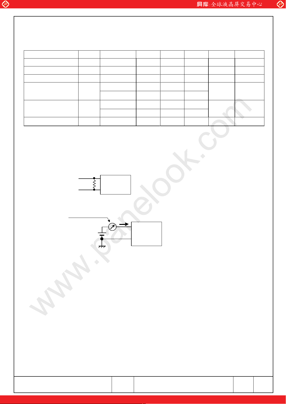
5.1 LCD CHARACTERISTICS
Item
Symbol
Condition Min. Typ. Max. Unit Remarks
$
a
Power Supply Voltage VDD - 3.0 3.3 3.6 V -
Ripple Voltage VRP - - - 100 mVp-p
Rush Current I
Differential Input
Voltage for LVDS
Receiver Threshold
- - - 2.0 A Note 1
RUSH
- - +100
V
V
I
IH
VIL -100 - -
mV Note 2
White Pattern - 410 510
Power Supply Current IDD
mA Note 3,4
Black Pattern - 590 690
DCLK Frequency
- - 65 80 MHz -
f
CL
Note 1: Rush current is set maximum 2A. Current capacity for VDD power supply should be larger than
5A, so that fuse built in the LCM could appropriately work under the abnormal condition.
Note 2: V
=+1.2V
CM
The input terminal of LVDS transmitter is terminated with 100.
IN+
100
IN-
LVDS
Receiver
0VV,25
SS
CT
Note 3: f
=65.0MHz, and VDD=3.3V, are the test conditions.
CLK
DC Ampere Meter
V
DD
I
DD
TFT-LCM
V
DD
V
SS
Note 4: For LVDS Transmitter Input
KAOHSIUNG OPTO-ELECTRONICS INC.
One step solution for LCD / PDP / OLED panel application: Datasheet, inventory and accessory!
SHEET
NO.
7B64PS 2705-TX38D18VM2BAA-1
PAGE
5-1/2
www.panelook.com
Page 6
Global LCD Panel Exchange Center
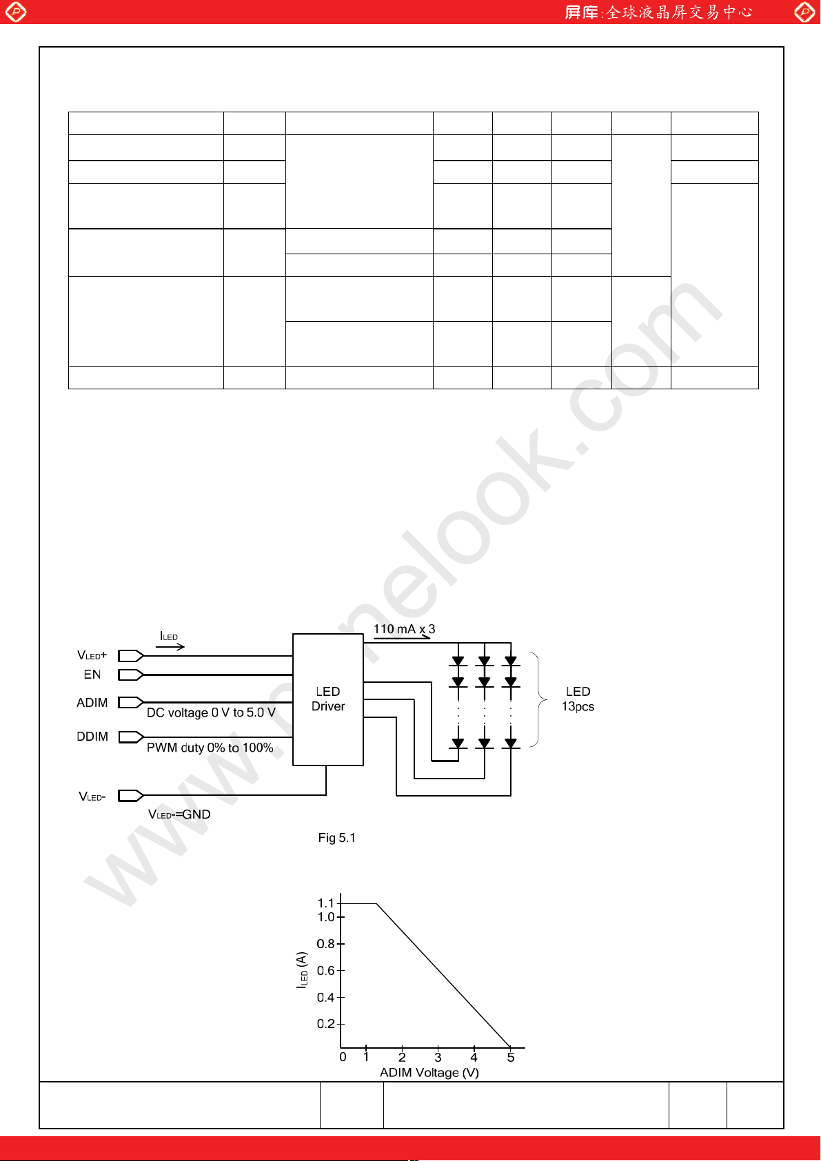
5.2 BACKLIGHT CHARACTERISTICS
www.panelook.com
$
CT
25
a
Item
LED Input Voltage
Enable EN 4.5 5 5.5 -
Analog Dimming
Function
Digital Dimming
Function
Symbol
V
LED
Condition Min. Typ. Max. Unit Remarks
10.8 12.0 13.2
Note 1
Backlight Unit
ADIM 0 5 5.5
“H” Level
4.0 5 5.5
V
DDIM
“L” Level 0 0 0.2
Note 2,3
ADIM = 0V,
LED Driving Current
(DIM Control)
I
LED
DDIM = 0% Duty
ADIM = 5V,
- (1100) -
mA
- (55) -
DDIM = 100% Duty
LED Lifetime - 110mA x 3 - (50k) - hrs Note 4
Note 1: As Fig 5.1 shown, all LEDs are controlled by the LED Driver when applying 12V V
LED
.
Note 2: Dimming function can be obtained by applying DC voltage or PWM signal from the display
interface CN2. The recommend PWM signal is 1KHz~10KHz with 5V amplitude. The
brightness is increased when applied DC voltage of ADIM or PWM duty of DDIM is decreased.
Note 3: 4A fuse is built in the LED voltage control board, current capacity for V
power supply should
LED
be larger than 10A, so that the fuse built in the LED voltage control board could appropriately
work under the abnormal condition.
Note 4: The estimated lifetime is specified as the time to reduce 50% brightness by applying 110mA x 3
$
at 25
.
C
Note 5: I
vs DIM Voltage (Reference only)
LED
KAOHSIUNG OPTO-ELECTRONICS INC.
One step solution for LCD / PDP / OLED panel application: Datasheet, inventory and accessory!
SHEET
NO.
7B64PS 2705-TX38D18VM2BAA-1
PAGE
5-2/2
www.panelook.com
Page 7
T
T
T
T
Global LCD Panel Exchange Center
www.panelook.com
6. OPTICAL CHARACTERISTICS
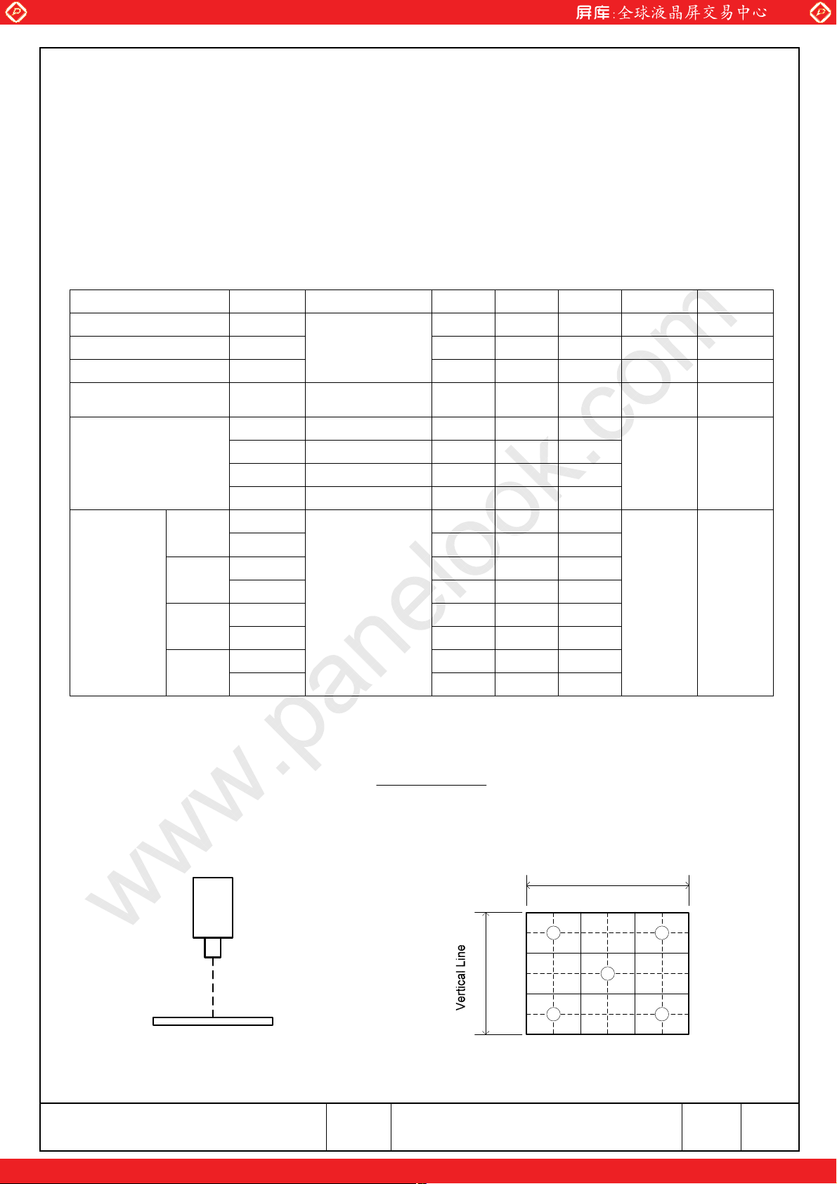
The optical characteristics are measured based on the conditions as below:
- Supplying the signals and voltages defined in the section of electrical characteristics.
- The backlight unit needs to be turned on for 30 minutes.
$
- The ambient temperature is 25
- In the dark room around 100~200 lx, the equipment has been set for the measurements as shown in
Fig 6.1.
Item
Brightness of White -
Brightness Uniformity - (70) 80 - % Note 2
Contrast Ratio CR (450) 700 - - Note 3
Response Time
Rising + Falling
(
)
Viewing Angle
Red
Green
Color
Chromaticity
Blue
White
Symbol
x
X
Y
X (0.29) 0.34 (0.39)
Y (0.55) 0.60 (0.65)
X (0.10) 0.15 (0.20)
Y (0.05) 0.10 (0.15)
X (0.28) 0.33 (0.38)
Y (0.30) 0.35 (0.40)
.
C
$
a
Condition Min. Typ. Max. Unit Remarks
2
cd/m
$$
0,0
TI
(960) 1200 -
,
Note 1
110mA x 3
TT
fr
c
x
y
c
y
$
I
$
I
$
I
I
$
$$
- 25 35 ms Note 4
0,0
TI
10 CR ,0 t
(70) 80 -
10 CR ,180 t
(70) 80 -
Degree Note 5
10 CR ,90 t
(60) 70 -
10 CR ,270 t
(70) 80 -
(0.57) 0.62 (0.67)
(0.30)
$$
0,0
TI
0.35
(0.40)
- Note 6
DD
VCT
3.3V,25
Note 1: The brightness is measured from the panel center point, P5 in Fig. 6.2, for the typical value.
Note 2: The brightness uniformity is calculated by the equation as below:
uniformity Brightness u
Brightness Min.
100%
Brightness Max.
, which is based on the brightness values of the 5 points measured by BM-5 as shown in Fig. 6.2.
Horizontal Line
D
Photo Detector: BM-5
$
1
Field:
Distance: 500 mm
LCD panel
KAOHSIUNG OPTO-ELECTRONICS INC.
SHEET
NO.
7B64PS 2706-TX38D18VM2BAA-1
W
3W/4
D/4 D/2 3D/4
W/4
W/2
1 2
3 4
5
Fig. 6.2 Fig. 6.1
PAGE
6-1/2
One step solution for LCD / PDP / OLED panel application: Datasheet, inventory and accessory!
www.panelook.com
Page 8
T
I
T
Global LCD Panel Exchange Center
www.panelook.com
Note 3: The Contrast Ratio is measured from the center point of the panel, P5, and defined as the
following equation:
CR
Whiteof Brightness
Black of Brightness
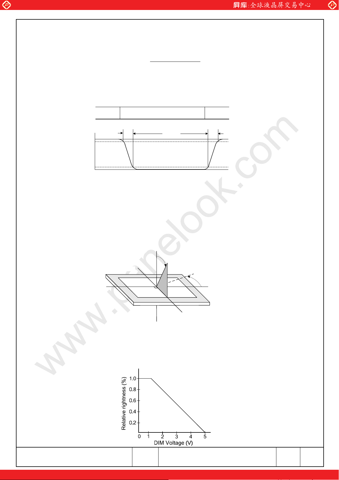
Note 4: The definition of response time is shown in Fig. 6.3. The rising time is the period from 90%
brightness to 10% brightness when the data is from white to black. Oppositely, Falling time is
the period from 10% brightness rising to 90% brightness.
WhiteWhite Black
Rising time Falling time
100 %
90
Brightness
10
0
Tr Tf
Fig . 6.3
Note 5: The definition of viewing angle is shown in Fig. 6.4. Angle I is used to represent viewing
directions, for instance,
$
means 6 o’clock, and
270
I
$
means 3 o’clock. Moreover, angle
0
I
is used to represent viewing angles from axis Z toward plane XY.
The viewing direction of this display is 12 o’clock, which means that a photograph with gray
scale would not be reversed in color and the brightness change would be less from this
direction. However, the best contrast peak would be located at 6 o’clock.
Ż
ľġViewing angle
90$
I
12 o'clock
180$
I
9 o'clock
ź
,0)y(x,
0$
I
xx'
3 o'clock
źĨ
270$
I
ŻĨ
6 o'clock
Fig 6.4
Note 6: The color chromaticity is measured from the center point of the panel, P5, as shown in Fig. 6.2.
Note 7: Relative Brightness V.S DIM Voltage (Reference only)
KAOHSIUNG OPTO-ELECTRONICS INC.
One step solution for LCD / PDP / OLED panel application: Datasheet, inventory and accessory!
SHEET
NO.
7B64PS 2706-TX38D18VM2BAA-1
PAGE
6-2/2
www.panelook.com
Page 9
Global LCD Panel Exchange Center
www.panelook.com
One step solution for LCD / PDP / OLED panel application: Datasheet, inventory and accessory!
www.panelook.com
Page 10
Global LCD Panel Exchange Center
www.panelook.com
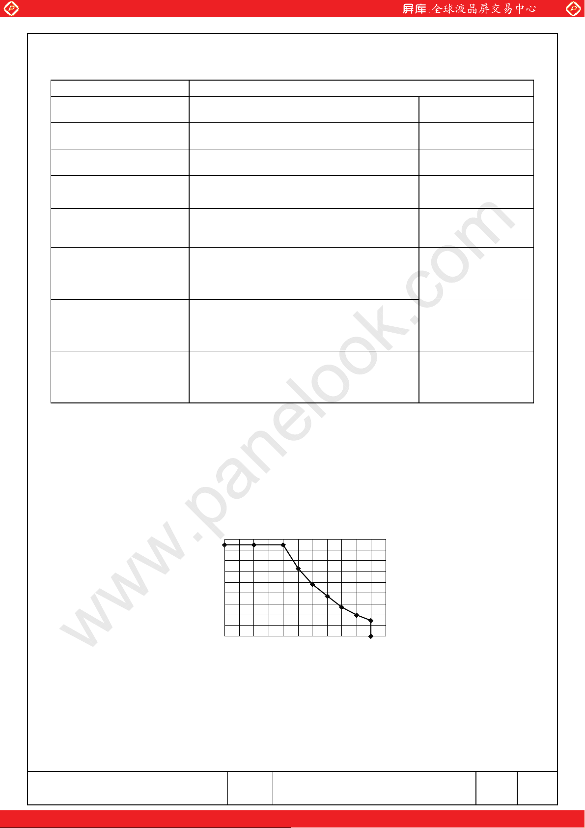
8. RELIABILITY TESTS
Test Item Condition
High Temperature
Low Temperature
High Temperature
Low Temperature
Thermal Shock
High Temperature &
Humidity
Vibration
ESD
1) Operating
2) 80ɗ
1) Operating
2) -30ɗ
1) Storage
2) 80ɗ
1) Storage
2) -30ɗ
1) Non-Operating
2) -30ɗ
3) 0.5 hr
1) Operating
2) 40ɗ& 85%RH
3) Without condensation
(Note3)
1) Non-Operating
2) 10㹼300 Hz
3) 1.5G
4) X, Y, and Z directions
5) Operating
6) Tip: 150 pF, 330ȟ,1 sec / cycle
7) Condition 1:Panel contact
8) Condition 2:Panel non-contact
l
l
80ɗ
0.5 hr
r
8KV
r
240 hrs
240 hrs
240 hrs
240 hrs
240 hrs
240 hrs
10 min / cycle, 3cycles
each direction
-
15KV
Note 1: Display functionalities are inspected under the conditions defined in the specification after the
reliability tests.
Note 2: The display is not guaranteed for use in corrosive gas environments.
Note 3: Under the condition of high temperature & humidity, if the temperature is higher than 40
humidity needs to be reduced as Fig. 8.1 shown.
!!
ɗ
, the
Note 4: Temperature of panel display surface area should be 80ɗ Max.
90
80
70
60
50
40
30
20
10
0
Relative Humidity RH (%)
20 25 30 35 40 45 50 55 60 65 70 75
$
Temperature Ta
Fig. 8.1
C)(
KAOHSIUNG OPTO-ELECTRONICS INC.
One step solution for LCD / PDP / OLED panel application: Datasheet, inventory and accessory!
SHEET
NO.
7B64PS 2708-TX38D18VM2BAA-1
PAGE
8-1/1
www.panelook.com
Page 11
Global LCD Panel Exchange Center
www.panelook.com
9. LCD INTERFACE
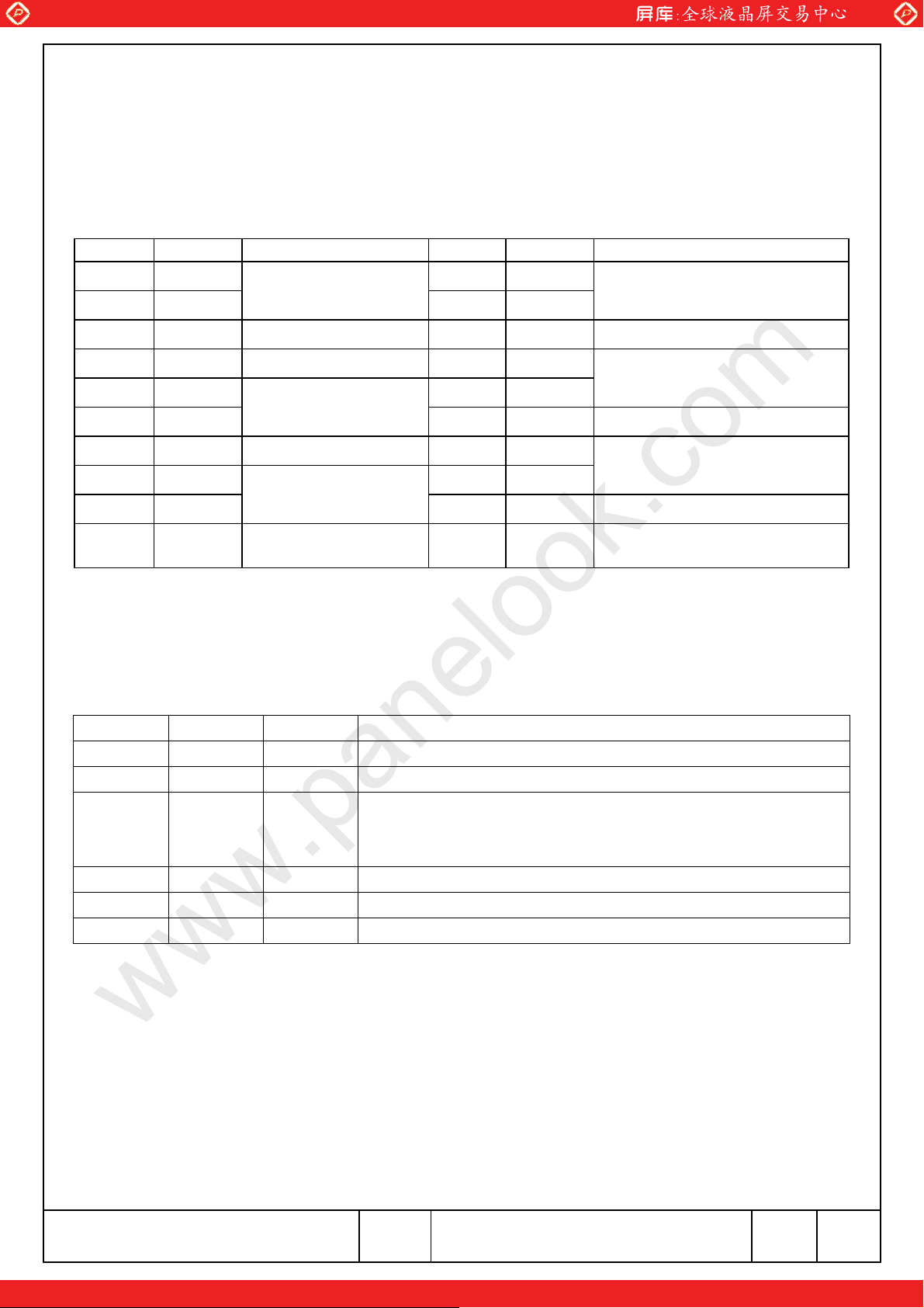
9.1 INTERFACE PIN CONNECTIONS
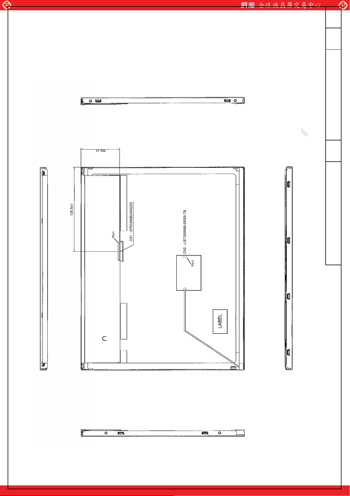
The display interface connector is MSB240420G made by STM and more details of the connector are
shown in the section of outline dimension.
Pin assignment of LCD interface is as below:
Pin No. Signal Function Pin No. Signal Function
1 V
2 VDD 12 IN2+
3 VSS GND 13 VSS GND
DD
Power Supply for Logic
11
IN2-
Pixel Data
4 NC No Connection 14 CLK IN-
5
6
7
8
9
10
IN0-
IN0+
V
SS
IN1-
IN1+
V
SS
Pixel Data
GND
Pixel Data
GND
15 CLK IN+
16 VSS GND
17 IN3-
18 IN3+
19 VSS GND
20 FRC
Clock
Pixel Data
High : 6 bit Mode (Note 2)
Low or NC : 8 bit Mode (Note 2)
Note 1: IN n- and IN n+ (n=0,1,2,3),CLK IN- and CLK IN+ are recommended to be twisted or
side-by-side FPC patterns, respectively.
Note 2:”High” stands for 3.3V, “Low” stands for 0V and “NC” stands for no connection.
The backlight interface connector is SM08B-SRSS-TB made by JST, and pin assignment of backlight is
as below:
Pin No. Signal Level Function
1,2 V
3 NC - No Connection
4 EN -
5 ADIM - Analog Voltage Dimming Function (Voltage Control)
6 DDIM - PWM Dimming Function
7,8 V
- Power Supply for LED
LED+
Enable Pin
High : Backlight Enable
Low : Backlight Disable
- - GND
LED
KAOHSIUNG OPTO-ELECTRONICS INC.
SHEET
NO.
7B64PS 2709-TX38D18VM2BAA-1
One step solution for LCD / PDP / OLED panel application: Datasheet, inventory and accessory!
PAGE
9-1/8
www.panelook.com
Page 12
Global LCD Panel Exchange Center
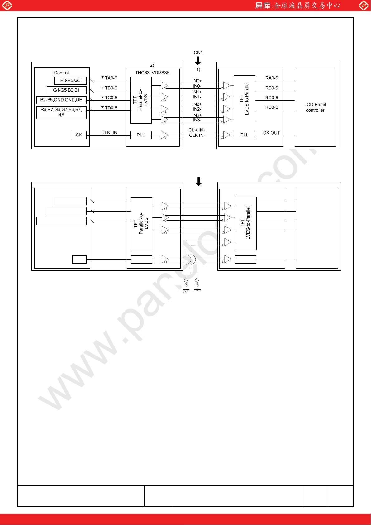
9.2 LVDS INTERFALE
(1) 8Bit Mode
FRC=Low or NC
www.panelook.com
(2) 6Bit Mode
FRC=High
Controll
R0-R5,G0
G1-G5,B0,B1
B2-B5,GND,GND,DE
CK
7 TA0-6
7 TB0-6
7 TC0-6
CLK IN
2)
THC63LVDM83R
PLL
470
470ȟ
CN1
1)
IN0+
IN0-
IN1+
IN1-
IN2+
IN2-
IN3+
IN3-
CLK IN+
CLK IN-
820
820ȟ
3.3V
PLL
RA0-6
RB0-6
RC0-6
RD0-6
CK OUT
Note 1) LVDS cable impedance should be 100 ohms per signal line when each
2-lines(+,-) is used in differential mode.
LCD Panel
controller
Note 2) Transmitter Made by Thine : THC63LVDM83R equivalent.
Transmitter is not contained in Module.
KAOHSIUNG OPTO-ELECTRONICS INC.
SHEET
NO.
7B64PS 2709-TX38D18VM2BAA-1
One step solution for LCD / PDP / OLED panel application: Datasheet, inventory and accessory!
PAGE
9-2/8
www.panelook.com
Page 13
Global LCD Panel Exchange Center
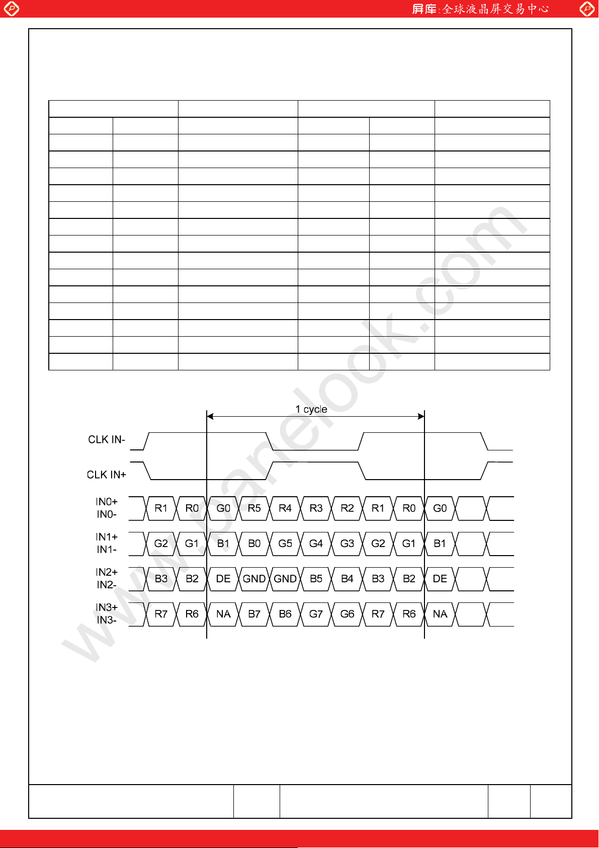
9.3 LVDS DATA MAPPING
1) THC63LVDM83R Pin Assignment (8 Bit Mode)
Transmitter FRC Transmitter FRC
Pin No. Date Low or NC Pin No. Date Low or NC
51 TA0 R0 (LSB) 20 TC0 B2
52 TA1 R1 22 TC1 B3
54 TA2 R2 23 TC2 B4
55 TA3 R3 24 TC3 B5
56 TA4 R4 27 TC4 GND
3 TA5 R5 28 TC5 GND
4 TA6 G0 (LSB) 30 TC6 DE
6 TB0 G1 50 TD0 R6
7 TB1 G2 2 TD1 R7 (MSB)
11 TB2 G3 8 TD2 G6
12 TB3 G4 10 TD3 G7 (MSB)
14 TB4 G5 16 TD4 B6
15 TB5 B0 (LSB) 18 TD5 B7 (MSB)
19 TB6 B1 25 TD6 NA
www.panelook.com
DE : Display Enable
NA : Not Available
KAOHSIUNG OPTO-ELECTRONICS INC.
SHEET
NO.
7B64PS 2709-TX38D18VM2BAA-1
One step solution for LCD / PDP / OLED panel application: Datasheet, inventory and accessory!
PAGE
9-3/8
www.panelook.com
Page 14
Global LCD Panel Exchange Center
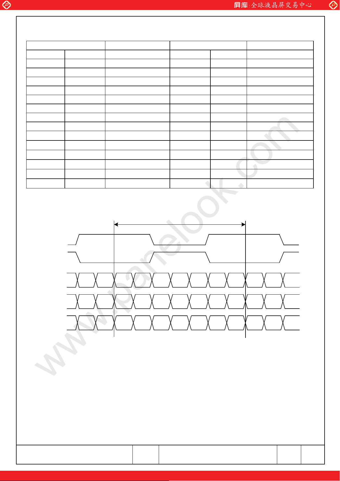
2) THC63LVDM83R Pin Assignment (6 Bit Mode)
Transmitter FRC Transmitter FRC
Pin No. Date High Pin No. Date High
51 TA0 R0 (LSB) 20 TC0 B2
52 TA1 R1 22 TC1 B3
54 TA2 R2 23 TC2 B4
55 TA3 R3 24 TC3 B5 (MSB)
56 TA4 R4 27 TC4 GND
3 TA5 R5 (MSB) 28 TC5 GND
4 TA6 G0 (LSB) 30 TC6 DE
6 TB0 G1 50 TD0 NA
7
11
12
14
15
19
TB1 G2
TB2 G3
TB3 G4
TB4 G5 (MSB)
TB5 B0 (LSB)
TB6 B1
www.panelook.com
2
8
10
16
18
25
TD1 NA
TD2 NA
TD3 NA
TD4 NA
TD5 NA
TD6 NA
CLK IN-
CLK IN+
IN0+
IN0-
IN1+
IN1-
IN2+
IN2-
DE : Display Enable
NA : Not Available.
1 cycle
R1 R0 G0 R5 R4 R3 R2 R1 R0 G0
G2 G1 B1 B0 G5 G4 G3 G2 G1 B1
B3 B2 DE GND GND B5 B4 B3 B2 DE
KAOHSIUNG OPTO-ELECTRONICS INC.
SHEET
NO.
7B64PS 2709-TX38D18VM2BAA-1
One step solution for LCD / PDP / OLED panel application: Datasheet, inventory and accessory!
PAGE
9-4/8
www.panelook.com
Page 15
Global LCD Panel Exchange Center
www.panelook.com
One step solution for LCD / PDP / OLED panel application: Datasheet, inventory and accessory!
www.panelook.com
Page 16
Global LCD Panel Exchange Center
www.panelook.com
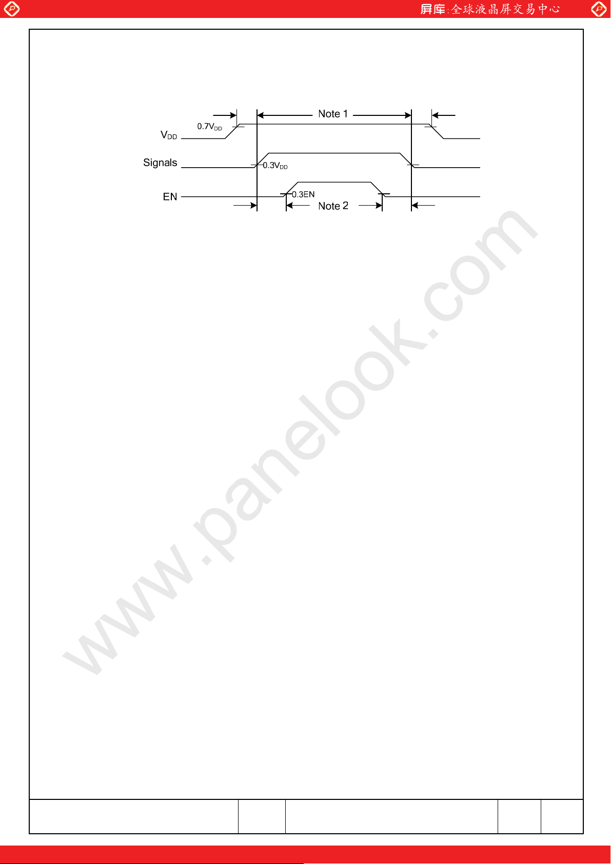
9.6 POWER SEQUENCE
Power Sequence Timing
Note 1: In order to avoid any damages, VDD has to be applied before all other signals. The opposite is
true for power off where V
The recommended time period is 1 second. Hot plugging might cause display damage due to
incorrect power sequence, please pay attention on interface connecting before power on.
has to be remained on until all other signals have been switch off.
DD
Note 2: In order to avoid showing uncompleted patterns in transient state. It is recommended that
switching the backlight on is delayed for 1 second after the signals have been applied. The
opposite is true for power off where the backlight has to be switched off 1 second before the
signals are removed.
Note 3: The floating state of interface signal shonld be avoid at invalid period.
Note 4: When the interface signal is invalid, please set the power supply of V
to 0V.
DD
KAOHSIUNG OPTO-ELECTRONICS INC.
SHEET
NO.
7B64PS 2709-TX38D18VM2BAA-1
One step solution for LCD / PDP / OLED panel application: Datasheet, inventory and accessory!
PAGE
9-6/8
www.panelook.com
Page 17
Global LCD Panel Exchange Center
www.panelook.com
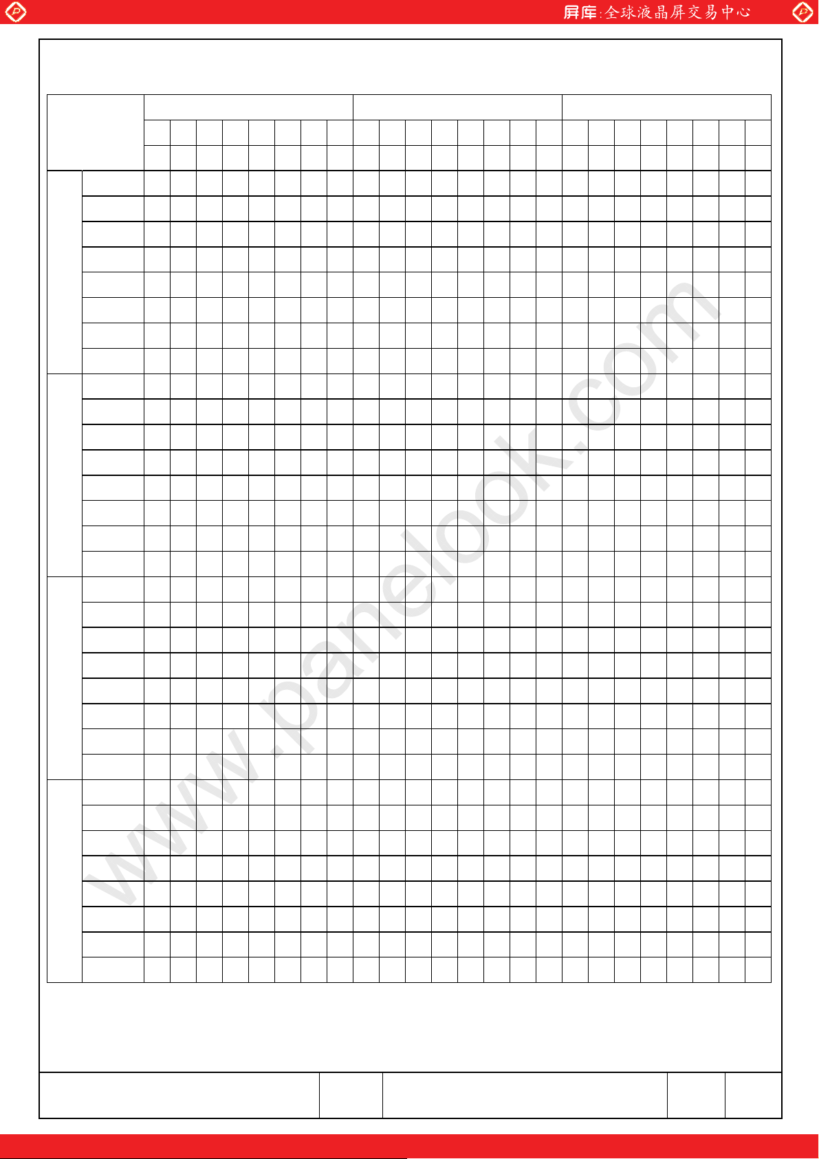
9.7 DATA INPUT for DISPLAY COLOR(8 BIT MODE)
Red Data Green Data Blue Data
Input color
Black 0 0 0 0 0 0 0 0000000000 0 0 0 0000
Red(255) 1 1 1 1 1 1 1 1 0 00000000 0 0 0 0000
Green(255) 0 0 0 0 0 0 0 0111111110 0 0 0 0000
Blue(255) 0 0 0 0 0 0 0 0 0 00000001 1 1 1 1111
Basic
Color
Red
Cyan 0 0 0 0 0 0 0 0111111111 1 1 1 1111
Magenta 1 1 1 1 1 1 1 1 0 00000001 1 1 1 1111
Yellow 1 1 1 1 1 1 1 1111111110 0 0 0 0000
White 1 1 1 1 1 1 1 1111111111 1 1 1 1111
Black 0 0 0 0 0 0 0 0000000000 0 0 0 0000
Red(1) 0 0 0 0 0 0 0 1 0 00000000 0 0 0 0000
Red(2) 0 0 0 0 0 0 1 0 0 00000000 0 0 0 0000
Red(253) 1 1 1 1 1 1 0 1 0 00000000 0 0 0 0000
R7 R6 R5 R4 R3 R2 R1 R0 G7 G6 G5 G4 G3 G2 G1 G0 B7 B6 B5 B4 B3 B2 B1 B0
MSB
: : : : : : : : ::::::::::: : : ::::
: : : : : : : : ::::::::::: : : ::::
LSB MSB LSB MSB
LSB
Red(254) 1 1 1 1 1 1 1 0 0 00000000 0 0 0 0000
Red(255) 1 1 1 1 1 1 1 1 0 00000000 0 0 0 0000
Black 0 0 0 0 0 0 0 0000000000 0 0 0 0000
Green(1) 0 0 0 0 0 0 0 0000000010 0 0 0 0000
Green(2) 0 0 0 0 0 0 0 0000000100 0 0 0 0000
Green
Blue
: : : : : : : : ::::::::::: : : ::::
: : : : : : : : ::::::::::: : : ::::
Green(253) 0 0 0 0 0 0 0 0111111010 0 0 0 0000
Green(254) 0 0 0 0 0 0 0 0111111100 0 0 0 0000
Green(255) 0 0 0 0 0 0 0 0111111110 0 0 0 0000
Black 0 0 0 0 0 0 0 0000000000 0 0 0 0000
Blue(1) 0 0 0 0 0 0 0 0000000000 0 0 0 0001
Blue(2) 0 0 0 0 0 0 0 0000000000 0 0 0 0010
: : : : : : : : ::::::::::: : : ::::
: : : : : : : : ::::::::::: : : ::::
Blue(253) 0 0 0 0 0 0 0 0 0 00000001 1 1 1 1101
Blue(254) 0 0 0 0 0 0 0 0 0 00000001 1 1 1 1110
Blue(255) 0 0 0 0 0 0 0 0 0 00000001 1 1 1 1111
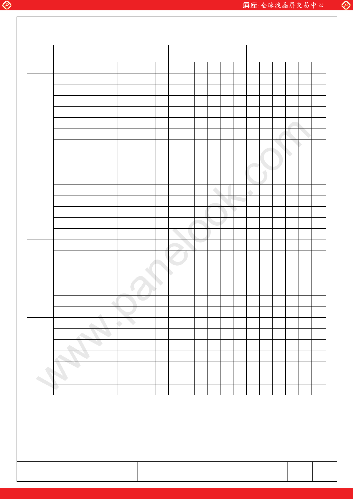
Note 1: Definition of gray scale : Color(n) Number in parenthesis indicates gray scale level. Larger
number corresponds to brighter level.
Note 2: Data Signal : 1 : High, 0 : Low
KAOHSIUNG OPTO-ELECTRONICS INC.
SHEET
NO.
7B64PS 2709-TX38D18VM2BAA-1
One step solution for LCD / PDP / OLED panel application: Datasheet, inventory and accessory!
PAGE
9-7/8
www.panelook.com
Page 18
Global LCD Panel Exchange Center
www.panelook.com
9.8 DATA INPUT for DISPLAY COLOR (6 BIT MODE)
Basic
Color
Red
COLOR &
Gray Scale
Black
Red (63)
Green (63)
Blue (63)
Cyan
Magenta
Yellow
White
Black
Red (1)
Red (2)
:
:
Red (62)
Red Data Green Data Blue Data
R5 R4 R3 R2 R1 R0 G5 G4 G3 G2 G1 G0 B5 B4 B3 B2 B1 B0
0 0 0 0 000000000 0 0 00 0
1 1 1 1 110000000 0 0 00 0
0 0 0 0 001111110 0 0 00 0
0 0 0 0 000000001 1 1 11 1
0 0 0 0 001111111 1 1 11 1
1 1 1 1 110000001 1 1 11 1
1 1 1 1 111111110 0 0 00 0
1 1 1 1 111111111 1 1 11 1
0 0 0 0 000000000 0 0 00 0
0 0 0 0 010000000 0 0 00 0
0 0 0 0 100000000 0 0 00 0
: : : : : : : : : : : : : : : : : :
: : : : : : : : : : : : : : : : : :
1 1 1 1 100000000 0 0 00 0
Green
Blue
Red (63)
Black
Green (1)
Green (2)
:
:
Green (62)
Green (63)
Black
Blue (1)
Blue (2)
:
:
Blue (62)
Blue (63)
1 1 1 1 110000000 0 0 00 0
0 0 0 0 000000000 0 0 00 0
0 0 0 0 000000010 0 0 00 0
0 0 0 0 000000100 0 0 00 0
: : : : : : : : : : : : : : : : : :
: : : : : : : : : : : : : : : : : :
0 0 0 0 001111100 0 0 00 0
0 0 0 0 001111110 0 0 00 0
0 0 0 0 000000000 0 0 00 0
0 0 0 0 000000000 0 0 00 1
0 0 0 0 000000000 0 0 01 0
: : : : : : : : : : : : : : : : : :
: : : : : : : : : : : : : : : : : :
0 0 0 0 000000001 1 1 11 0
0 0 0 0 000000001 1 1 11 1
KAOHSIUNG OPTO-ELECTRONICS INC.
SHEET
NO.
7B64PS 2709-TX38D18VM2BAA-1
One step solution for LCD / PDP / OLED panel application: Datasheet, inventory and accessory!
PAGE
9-8/8
www.panelook.com
Page 19
Global LCD Panel Exchange Center
www.panelook.com
10-1/2
PAGE
7B64PS 2710-TX38D18VM2BAA-1
No.
SHEET
KAOHSIUNG OPTO-ELECTRONICS INC.
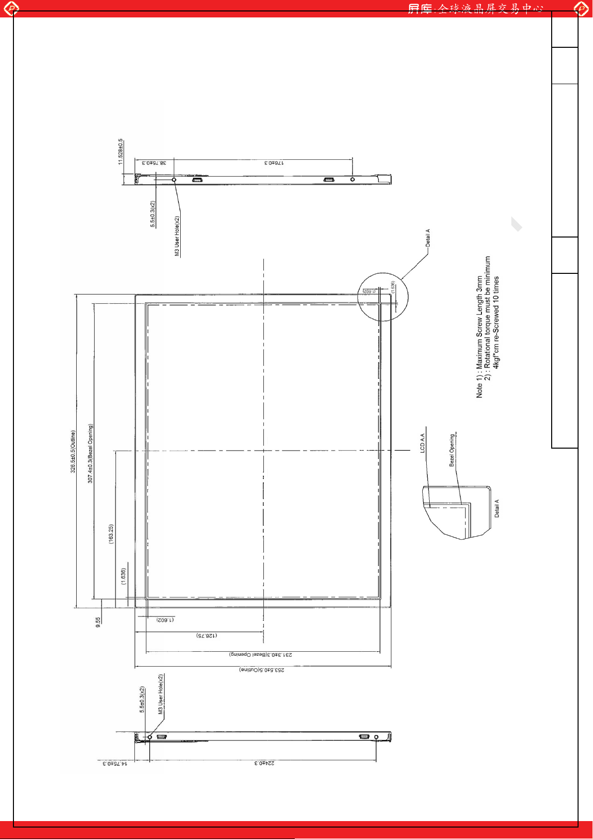
10.1 FRONT VIEW
10. OUTLINE DIMENSIONS
One step solution for LCD / PDP / OLED panel application: Datasheet, inventory and accessory!
www.panelook.com
Page 20
Global LCD Panel Exchange Center
www.panelook.com
10-2/2
PAGE
7B64PS 2710-TX38D18VM2BAA-1
No.
SHEET
KAOHSIUNG OPTO-ELECTRONICS INC.
9.2 FRAR VIEW
One step solution for LCD / PDP / OLED panel application: Datasheet, inventory and accessory!
www.panelook.com
Page 21
Global LCD Panel Exchange Center
T
T
www.panelook.com
11. APPEARANCE STANDARD
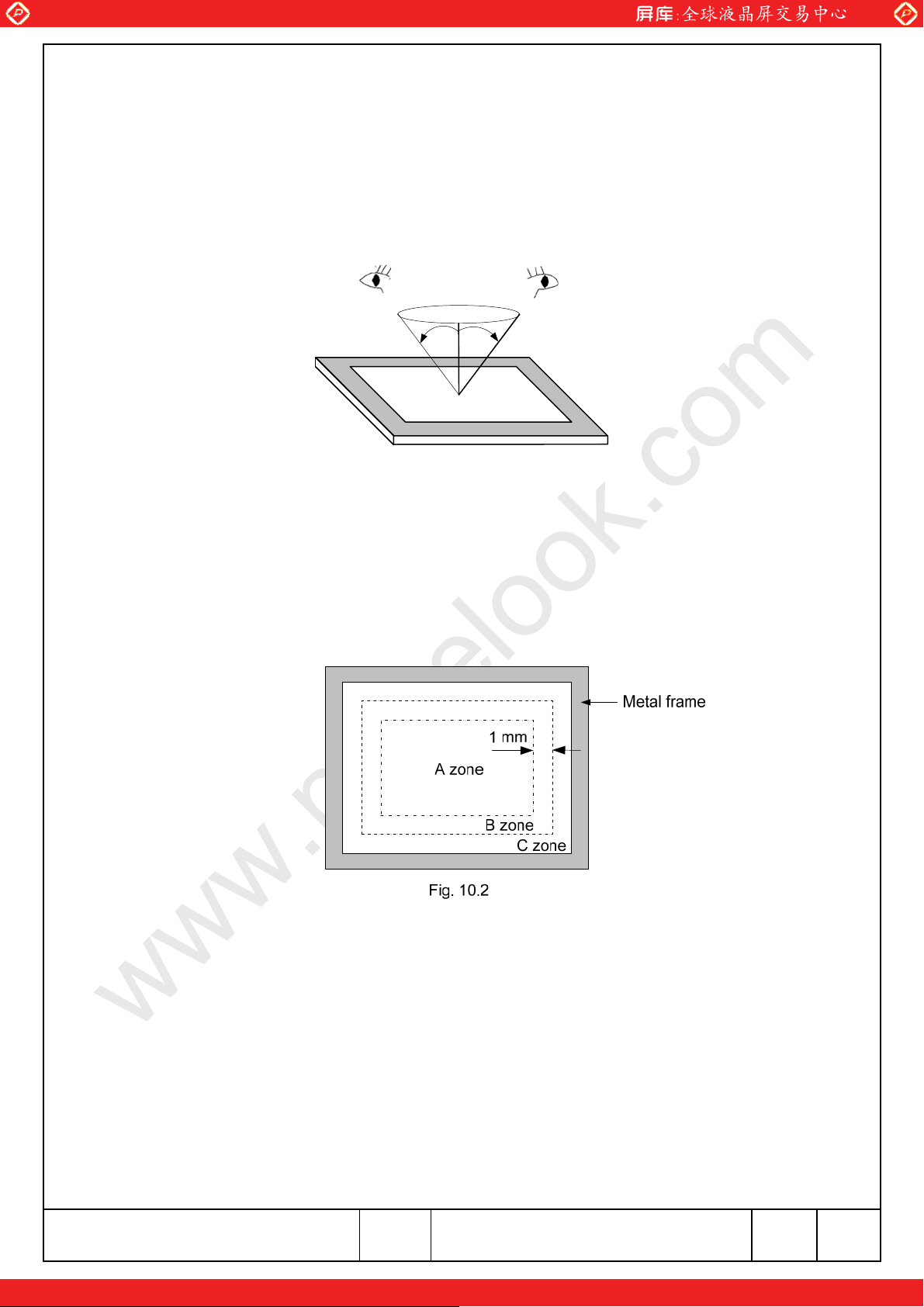
The appearance inspection is performed based on the conditions as below:
- The distance between inspector’s eyes and display is 35 cm.
- Ambient illumination:100~200 lx for light on inspection.
- The viewing angle to the front surface of display panel is 15 degree in vertical direction and 45 degree
in horizontal direction.
Fig. 10.1
11.1 THE DEFINITION OF LCD ZONE
LCD panel is divided into 3 areas as shown in Fig.10.2 for appearance specification in next section. A
zone is the LCD active area (dot area); B zone is the area, which extended 1 mm out from LCD active
area; C zone is the area between B zone and metal frame.
In terms of housing design, B zone is the recommended window area customers’ housing should be
located in.
KAOHSIUNG OPTO-ELECTRONICS INC.
One step solution for LCD / PDP / OLED panel application: Datasheet, inventory and accessory!
SHEET
NO.
7B64PS 2711-TX38D18VM2BAA-1
PAGE
11-1/3
www.panelook.com
Page 22
Global LCD Panel Exchange Center
www.panelook.com
11.2 LCD APPEARANCE SPECIFICATION
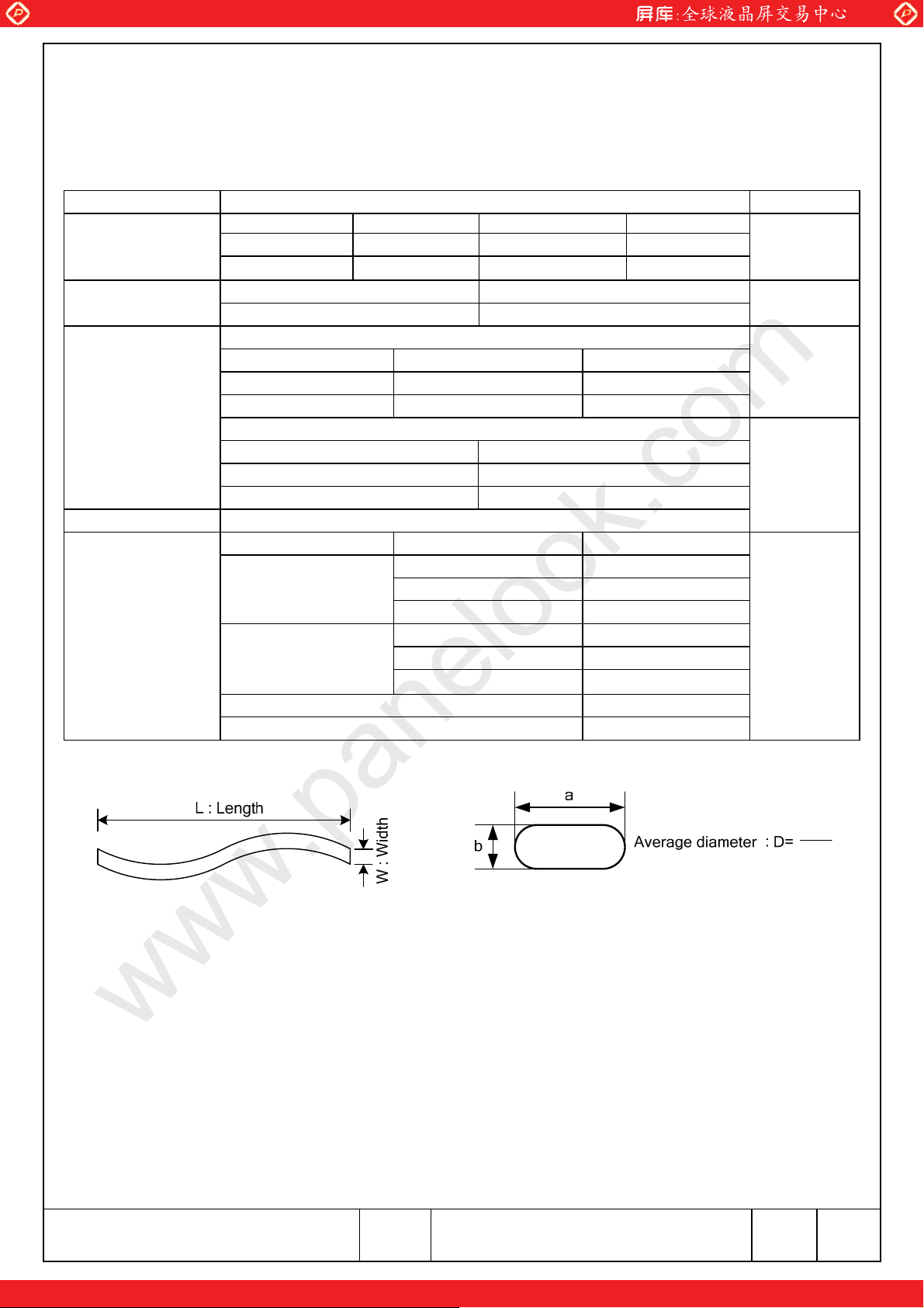
The specification as below is defined as the amount of unexpected phenomenon or material in a zone
(LCD active area) panel. The definitions of length, width and average diameter using in the table are
shown in Fig. 11.3.
Item Criteria Applied zone
Scratches on
polarizer
Bubbles / Dent
1) Foreign Materials
2) Dark / White Spot
Stain on polarizer Those wiped out easily are acceptable
Dot-Defect
(Note 1)
Length (mm) Width (mm) Maximum number Minimum space
- Wʀ0.05 Ignored -
0.3烋Lʀ10 0.05烋Wʀ0.1 4 -
Average diameter (mm) Maximum number
0.15烋Dʀ0.5 4
Filamentous (Line shape)
Length (mm) Width (mm) Maximum number
- Wʀ0.05 Ignored
0.3烋Lʀ2.0 0.05烋Wʀ0.1 4
Round (Dot shape)
Average diameter (mm) Maximum number
Dʀ0.15 Ignored
0.15ʀD烋0.5 4
Type Maximum number
1 dot 3
Bright dot-defect
Dark dot-defect
In total 5
Minimum distance 10 mm
2 adjacent dots 1
3 adjacent dots or above Not allowed
1 dot 5
2 adjacent dots 1
3 adjacent dots or above Not allowed
A
A
A
A
A
KAOHSIUNG OPTO-ELECTRONICS INC.
SHEET
NO.
Fig 11.3
7B64PS 2711-TX38D18VM2BAA-1
PAGE
ba
2
11-2/3
One step solution for LCD / PDP / OLED panel application: Datasheet, inventory and accessory!
www.panelook.com
Page 23
Global LCD Panel Exchange Center
Note 1: The definitions of dot defect are as below:
- The defect area of the dot must be bigger than half of a dot.
- For bright dot-defect, the dot’s appear bright and unchanged in size under showing black
pattern.
- For dark dot-defect, the dot’s appear dark and unchanged in size under pure red, green, blue
and white pattern.
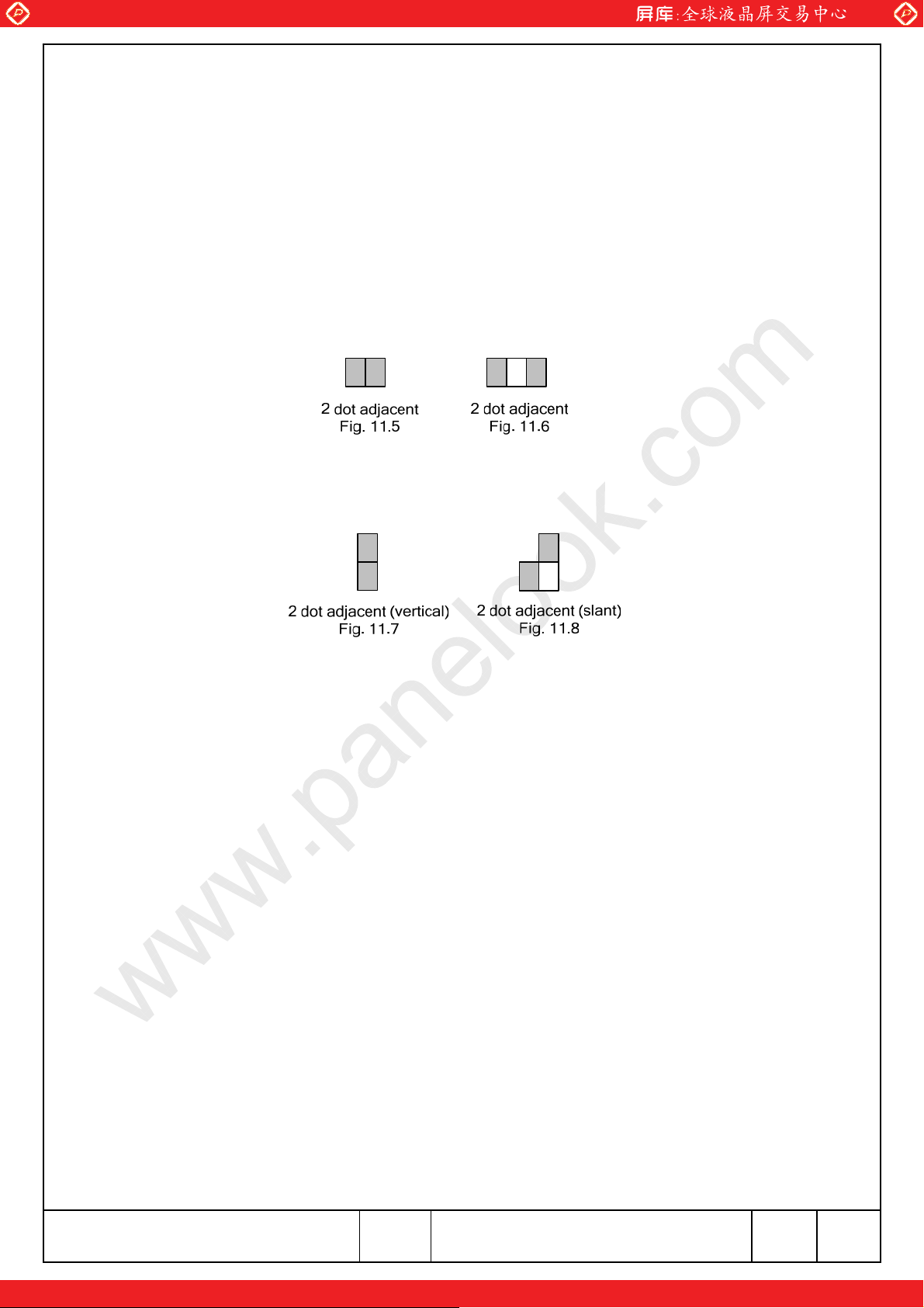
- The definition of 1-dot-defect is the defect-dot, which is isolated and no adjacent defect-dot.
- The definition of adjacent dot is shown as Fig. 11.5 to Fig 11.8.
www.panelook.com
KAOHSIUNG OPTO-ELECTRONICS INC.
SHEET
NO.
7B64PS 2711-TX38D18VM2BAA-1
One step solution for LCD / PDP / OLED panel application: Datasheet, inventory and accessory!
PAGE
11-3/3
www.panelook.com
Page 24
Global LCD Panel Exchange Center
www.panelook.com
12. PRECAUTIONS
12.1 PRECAUTIONS of ESD
1) Before handling the display, please ensure your body has been connected to ground to avoid any
damages by ESD. Also, do not touch display’s interface directly when assembling.
2) Please remove the protection film very slowly before turning on the display to avoid generating ESD.
12.2 PRECAUTIONS of HANDLING
1) In order to keep the appearance of display in good condition, please do not rub any surfaces of the
displays by using sharp tools harder than 3H, especially, metal frame and polarizer.
2) Please do not stack the displays as this may damage the surface. In order to avoid any injuries,
please avoid touching the edge of the glass or metal frame and wore gloves during handling.
3) Touching the polarizer or terminal pins with bare hand should be avoided to prevent staining and
poor electrical contact.
4) Do not use any harmful chemicals such as acetone, toluene, and isopropyl alcohol to clean display’s
surfaces.
5) Do not disassemble the module.
6) Please wipe any unknown liquids immediately such as saliva, water or dew on the display to avoid
color fading or any permanent damages.
7) Do not have pressure or impulse on the module because the module will be damage.
8) Please use soft cloth without chemicals to clean the display by gently wiping.
KAOHSIUNG OPTO-ELECTRONICS INC.
One step solution for LCD / PDP / OLED panel application: Datasheet, inventory and accessory!
SHEET
NO.
7B64PS 2711-TX38D18VM2BAA-1
PAGE
12-1/2
www.panelook.com
Page 25
Global LCD Panel Exchange Center
www.panelook.com
12.3 PRECAUTIONS of OPERATING
1) Please input signals and voltages to the displays according to the values defined in the section of
electrical characteristics to obtain the best performance. Any voltages over than absolute maximum
rating will cause permanent damages to this display. Also, any timing of the signals out of this
specification would cause unexpected performance.
2) When the display is operating at significant low temperature, the response time will be slower than it
$
C
at 25
.
3) The use of screen saver or sleep mode is recommended when static images are likely for long
periods of time. This is to avoid the possibility of image sticking.
4) Spike noise can cause malfunction of the circuit. The recommended limitation of spike noise is no
bigger than 100 mV p-p.
5) Moisture come into or contact the LCD module may damage LCD module when it is operating.
6) The LED driver board with cable can’t be pulled strongly or cable connector will be damaged.
12.4 PRECAUTIONS of STORAGE
If the displays are going to be stored for years, please be aware the following notices.
1) Please store the displays in a dark room to avoid any damages from sunlight and other sources of
UV light.
2) Please store LCD module within the specified storage conditions.
3) It would be better to keep the displays in the container, which is shipped from KOE, and do not
unpack it.
4) Please do not stick any labels on the display surface for a long time, especially on the polarizer.
KAOHSIUNG OPTO-ELECTRONICS INC.
SHEET
NO.
7B64PS 2711-TX38D18VM2BAA-1
One step solution for LCD / PDP / OLED panel application: Datasheet, inventory and accessory!
PAGE
12-2/2
www.panelook.com
Page 26
Global LCD Panel Exchange Center
www.panelook.com
13. DESIGNATION of LOT MARK
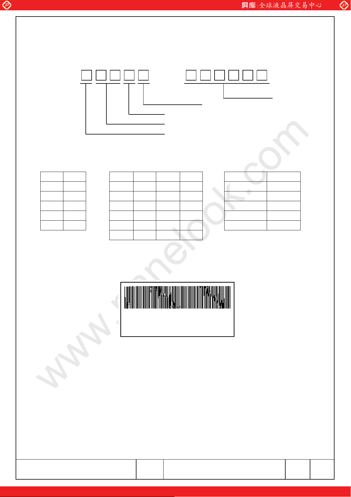
1) The lot mark is showing in Fig.13.1. First 4 digits are used to represent production lot, T represented
made in Taiwan, and the last 6 digits are the serial number.
2 1 0 1 T 0 0 0 0 0 1
Serial number
T : Made in Taiwan
Week
Month
Year
2) The tables as below are showing what the first 4 digits of lot mark are shorted for.
Year Mark
2012 2
2013 3
2014 4
2015 5
2016 6
Month Mark Month Mark
1 01 7 07
2 02 8 08
3 03 9 09
4 04 10 10
5 05 11 11
6 06 12 12
Week (Days) Mark
1~7 1
8~14 2
15~21 3
22~28 4
29~31 5
3) Except letters I and O, revision number will be shown on lot mark and following letters A to Z.
4) The location of the lot mark is on the back of the display shown in Fig. 13.1.
TX38D18VM2BAA REV:A
2101T 00001
KOE MADE IN TAIWAN
Fig. 13.1
KAOHSIUNG OPTO-ELECTRONICS INC.
SHEET
NO.
7B64PS 2711-TX38D18VM2BAA-1
One step solution for LCD / PDP / OLED panel application: Datasheet, inventory and accessory!
PAGE
13-1/1
www.panelook.com
 Loading...