

Page 1
Hitachi Displays, Ltd.
Date; Sep. 8, 2003
For Messrs. Hitachi Europe Ltd.
CUSTOMER'S ACCEPTANCE SPECIFICATIONS
TX18D16VM1CAA
CONTENTS
No. Item Sheet No. Page
- COVER 3284PS 2601-TX18D16VM1CAA-1 1-1/1
- RECORD OF REVISION 3284PS 2602-TX18D16VM1CAA-1 2-1/1
- DESCRIPTION 3284PS 2603-TX18D16VM1CAA-1 3-1/1
1 ABSOLUTE MAXIMUM RATINGS 3284PS 2604-TX18D16VM1CAA-1 4-1/1
2 OPTICAL CHARACTERISTICS 3284PS 2605-TX18D16VM1CAA-1 5-1/2 - 5-2/2
3 ELECTRICAL CHARACTERISTICS 3284PS 2606-TX18D16VM1CAA-1 6-1/1
4 BLOCK DIAGRAM 3284PS 2607-TX18D16VM1CAA-1 7-1/1
5 INTERFACE PIN CONNECTION 3284PS 2608-TX18D16VM1CAA-1 8-1/2 - 8-2/2
6 INTERFACE TIMING 3284PS 2609-TX18D16VM1CAA-1 9-1/3 - 9-3/3
7 DIMENSIONAL OUTLINE 3284PS 2610-TX18D16VM1CAA-1 10-1/1
8 DESIGNATION OF LOT MARK 3284PS 2611-TX18D16VM1CAA-1 11-1/1
9 COSMETIC SPECIFICATIONS 3284PS 2612-TX18D16VM1CAA-1 12-1/3 - 12-3/3
10 PRECAUTIONS 3284PS 2613-TX18D16VM1CAA-1 13-1/3 - 13-3/3
Please return 1 copy with your signature on this page for approval.
Accepted by : Proposed by :
Date :
Hitachi Displays, Ltd.
Sh.
No.
CAS-S03-154
3284PS 2601-TX18D16VM1CAA-1 Page 1-1/1
Page 2
Date
RECORD OF REVISION
The upper section:Before revision
The lower section:After revision
Sheet No. Page
Summary
Hitachi Displays, Ltd.
Date
Sep.8,2003
Sheet
No.
3284PS 2602-TX18D16VM1CAA-1
Page
2-1/1
Page 3
Color Pixel Arrangement
Display Mode
12 o'clock. (The direction it's hard to be discolored)
DESCRIPTION
with Back-light unit.
The specifications are applied to the following TFT Liquid Crystal Display Module
Note : Inverter device for Back-Light is not built in, so it should
be prepared by yourself .
Product name TX18D16VM1CAA
Effective Display Area (H)152.4 x (V)91.44 [mm]
Display Dots (H)(800x3) x (V)480 [dots]
(Display Pixels) (H 800 x V 480) [pixels]
Pixel Pitch (H)0.1905 x (V)0.1905 [mm]
R+G+B Vertical Stripe
Transmissive Mode, Normally White Mode
Surface Polarizing Film Polarizing Film with Antiglare Coating
Number of Colors 262k [colors]
Interface C-MOS, R.G.B x 6 bit Digital each
Color Saturation 60%(typ) for NTSC
Viewing Angle
Backlight CCFL, 1pc Side-light type (U shape)
Dimensions Outline (H)165.0(typ) x (V)106.0(typ) x (t)10.5(max) [mm]
Weight Approximately 170 [g]
Hitachi Displays, Ltd.
Date
Sep.8,2003
Sheet
No.
3284PS 2603-TX18D16VM1CAA-1
Page
3-1/1
Page 4
Operating
Non-operation
2)
2)
NotAcceptable
NotAcceptable
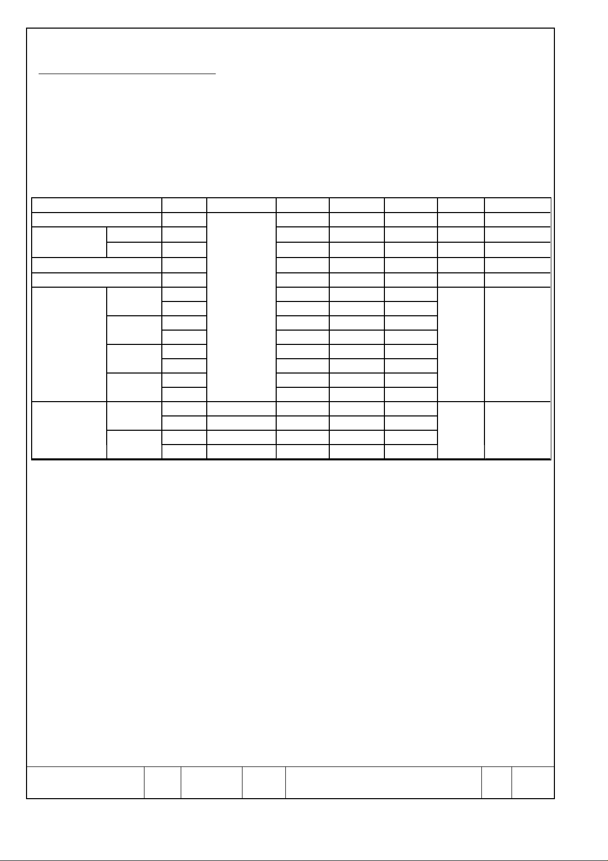
1. ABSOLUTE MAXIMUM RATINGS
1.1 ENVIRONMENTAL ABSOLUTE MAXIMUM RATINGS
Item
Temperature
Humidity
Vibration
Shock
Min. Max. Min. Max. Unit Note
0 70 -20
70
℃
1)
%RH 1)
─ ─
4.9 (0.5G)
─ ─
19.6 (2G)
490 (50G)
m/s2 3)
m/s2 4)
Corrosive Gas
Illumination at
LCD Surface
Notes 1) "Temperature" and "Humidity" shall be at glass surface of a TFT-LCD Module, not in the
system installed with the Module.
It's should not be over these absolute maximum ratings at any position of a TFT-LCD Module.
Operating temperature means the temperature a TFT-LCD Module can be driven, not mean
guarantee the screen performance (contrast,brightness,response time etc) is judged
at Ta=25deg.C
At low temperature the brightness of CCFL drop and the life time of CCFL become to be short.
2) Ambient temp. Ta≦40 ℃ : 85 % RH Max. Without condensation.
Ta>40 ℃ : Absolute humidity must be lower than the humidity of 85 %
at 40 deg.C. Without condensation.
3) Frequency of the vibration shall be between 20 Hz and 50 Hz. (except resonance point)
4) Pulse width of the shock shall be 7 ms.
─
50,000
─
50,000 lx
1.2 ELECTRICAL ABSOLUTE MAXIMUM RATINGS
(1) TFT LIQUID CRYSTAL DISPLAY MODULE
VSS=0V
Item Symbol Min. Max. Unit Note
Power Supply Voltage for logic VDD 0
4.0
V
Input signal Voltage for logic VI -0.2 VDD+0.2 V 1)
Electrostatic Durability VESD0
VESD1
Notes 1) The specification is applied to pixel data signal,timing signal and clock signal.
2) Discharge circuit to be connected : 200 pF - 250 Ω, Environmental : 25℃ - 70 % RH
3) The specification is applied to I/F connector pins.
4) The specification is applied to the surface of both a metal bezel and a LCD panel.
(2) BACK-LIGHT UNIT
±
±
100
8
V 2), 3)
kV 2), 4)
GND=0V
Item Symbol Min. Max. Unit Note
Lamp Current IL - 7.0
Lamp Voltage VL - 2000
Notes 1) To be measured at GND terminal side
2) The specification is applied at connector pins for back-light units .
mArms 1)
Vrms 2)
Hitachi Displays, Ltd.
Date
Sep.8,2003
Sheet
No.
3284PS 2604-TX18D16VM1CAA-1
Page
4-1/1
Page 5
Brightness (White)
Brightness Uniformity
2. OPTICAL CHARACTERISTICS
The following items are measured on the conditions that this unit operation (TFT panel and the
Back-light) and measuring systems are stable. It takes about 15 minutes.
The ambient light excluding The Back-light unit is nothing.
・Measuring equipment : TOPCON BM-7,Prichard 1980A, or equivalent
・Measuring point : Active area center
Ta = 25 ℃, VDD = 3.3 V, fV = 60 Hz, IL= 4.0mA
Item Symbol Conditions Min. Typ. Max. Unit Note
Contrast Ratio CR 100 200
Response Time RISE ton
FALL toff
─
─
20 40 ms 3)
10 20 ms 3)
Bwh 300 350
Buni 70
─ ─
Color Position Red x 0.57 0.62 0.67
on CIE y
θ=0℃
0.29 0.34 0.39
Green x 1) 0.24 0.29 0.34
y 0.55 0.60 0.65
Blue x 0.09 0.14 0.19
y 0.02 0.07 0.12
White x 0.25 0.30 0.35
y 0.26 0.31 0.36
x−x' θx θ=0°
Viewing Angle
θx' θ=180°
(CR≧10) y−y' θy θ=90°
θy' θ=270°
50
50
50
50
─ ─
─ ─
─ ─
─ ─
─
─
cd/m2
% 4)
─
deg. 1)
2)
Hitachi Displays, Ltd.
Date
Sep.8,2003
Sheet
No.
3284PS 2605-TX18D16VM1CAA-1
Page
5-1/2
Page 6
Notes
1)
Defin
ition of Viewing Angle
CR =(Luminance at displaying WHITE )
X(3 o'clock
270
6 o'clock
TFT
LCD Module
180
9 o'clock
12 o'clock
φ
Y'Z'X'YZθeye
data signal
BLACK
WHITE
BLACK
Luminance
01090
100%ton
toff
2) Definition of Contrast Ratio(CR):
(Luminance at displaying BLACK)
3) Definition of Response Time
4)Definition of Brightness Uniformity
The brightness uniformity (Buni
) is def
ined as the following equation.
(3)
(4)
10
509
0%9
0
5010
%
Buni=Bmin
Bmax
100
:measuring point
(Azimuth)
(Viewing Angle)
Display
Area
Area
(
θ=0°
φ=90°
)
(
φ=
°
)
Displaying
‑
φ=
(
φ=0°
)
°
)
Optical Response
(
Display
Hitachi Displays, Ltd.
)
(1) (2)
(5)
Date
Sep.8,2003
×
where, Bmax = Maximum brightness among 5 measuring points
Bmin = Minimum brightness among 5 measuring points
Sheet
No.
3284PS 2605-TX18D16VM1CAA-1
Page
5-2/2
Page 7
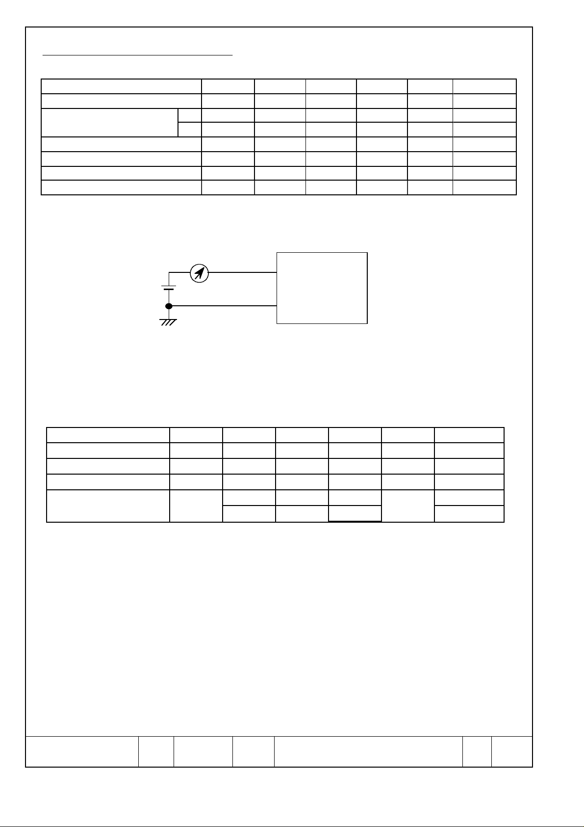
3. ELECTRICAL CHARACTERISTICS
3.1 TFT LIQUIDO CRYSTAL DISPLAY MODULE
Item Symbol Min. Typ. Max. Unit Note
Power Supply Voltage VDD 3.0 3.3 3.6 V
Input Voltage for Hi VIH 2.0
Logic Circuits Lo VIL VSS
Power Supply Current IDD
VSYNC Frequency fV
HSYNC Frequency fH
DCLK Frequency fCLK
Notes 1) The specification is applied to pixel data signal,timing signal and clock signal.
2) fV=60Hz ,fCLK=33.3 MHz, VDD =3.3V, DC Current.
DC Ampere Meter
─
─
─
─
TFT -LCD Module
VDD
VSS
─
─
250 350 mA 2), 3)
60 75 Hz
31.6 39.2 kHz
33.3 40 MHz
Ta=25℃,VSS=0V
VDD V 1)
0.8 V 1)
Typical value is measured when displaying Black raster.
Maximum is measured when displaying Vertical-stripe pattern of 2 pixel pitch.
3) Current capacity for VDD power source should be larger than 2A.
This TFT-LCD Module has a fuse(1A).
3.2 BACK-LIGHT UNIT
Ta=25℃
Item Symbol Min. Typ. Max. Unit Note
Lamp Current IL 2.0 3.0 4.0 mArms
Lamp Voltage VL
Frequency fL 50
Starting Lamp Voltage VS 1400
Notes
1) Larger IL causes the shorter life of a CCFL.
2) Frequency of power supply for a CCFL may cause interference with HSYNC frequency and
causes beat or flicker on the display. Therefore, lamp frequency shall be as different as
possible from HSYNC frequency in order to avoid the interference.
3) To be measured at GND terminal side
4) Starting Lamp Votage should be kept 1 sec at least.
5) The inverter should be built-in a safety circuit which detects over current, over voltage
and distorted wave form of lamp current.
─
1600
1000
─
─
─
─
Vrms
70 kHz 2)
2000 Vrms Ta=25deg. C
2000 Ta=0deg. C
1),3)
Hitachi Displays, Ltd.
Date
Sep.8,2003
Sheet
No.
3284PS 2606-TX18D16VM1CAA-1
Page
6-1/1
Page 8
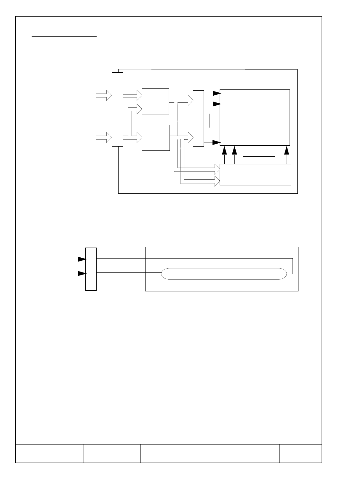
4. BLOCK DIAGRAM
4.1 TFT-LCD MODULE
Display data and
timing signal
CN1
Timing
Converter
G1
G2
DC power
supply
4.2 BACK-LIGHT UNIT
GND
VL
Gate
Driver
DC/DC
Converter
CN2
3
2
1
G480
Lamp
TFT-LCD
D1 D2 D2400
Drain Driver
Hitachi Displays, Ltd.
Date
Color of wires from CCFL to CN2
3 (GND):White
1 (VL) :Pink
Sep.8,2003 7-1/1
Sheet
No.
3284PS 2607-TX18D16VM1CAA-1
Page
Page 9

Pin No.
Symbol
Description
Note
1VLPower Supply
2NCNo connection
3
GND
GND(0V)
5. INTERFACE PIN CONNECTION
Pin No.
Symbol
Description
Note
1
VDD
Power Supply (typ.+3.3V)
1)2VDD
3
VDD
4
VDD
5NCNon-Connect
4)6DTMG
Display Timing
7
VSS
GND (0V)
2)8NC
Non-Connect
4)9VSS
GND (0V)
2)10(IC)3)11
VSS
GND (0V)
2)12B513B4
Blue Data
14B315
VSS
GND (0V)
2)16B217B1
Blue Data
18B019
VSS
GND (0V)
2)20G521G4
Green Data
22G323
VSS
GND (0V)
2)24G225G1
Green Data
26G027
VSS
GND (0V)
2)28R529R4
Red Data
30R331
VSS
GND (0V)
2)32R233R1
Red Data
34R035
(IC)3)36
VSS
GND (0V)
2)37VSS
38
DCLK
Dot Clock
39
VSS
GND (0V)
2)40VSS
5.1 TFT-LCD MODULE
CN1 《JAE ;FA5B040HF1R3000》
Notes 1) All VDD pins shall be connected to +3.3V(Typ.).
2) All VSS pins shall be grounded. Metal bezel is internally connected to VSS.
4) Unconnected to the module
5.2 BACK-LIGHT UNIT
CN2 《J.S.T. ; BHR-03VS-1》
Hitachi Displays, Ltd.
3) Keep open electrically. Hitachi test use only.
Date
Sep.8,2003
Sheet
No.
3284PS 2608-TX18D16VM1CAA-1
Page
8-1/2
Page 10

Red Data
Green Data
Blue Data
5.3 RELATIONSHIP BETWEEN DISPLAYED COLOR AND INPUT DATA
Input R5 R4 R3 R2 R1 R0 G5 G4 G3 G2 G1 G0 B5 B4 B3 B2 B1 B0
Color
Black 0 0 0 0 0 0 0 0 0 0 0 0 0 0 0 0 0 0
Red (0) 1 1 1 1 1 1 0 0 0 0 0 0 0 0 0 0 0 0
Green (0) 0 0 0 0 0 0 1 1 1 1 1 1 0 0 0 0 0 0
Basic Blue (0) 0 0 0 0 0 0 0 0 0 0 0 0 1 1 1 1 1 1
Color Cyan 0 0 0 0 0 0 1 1 1 1 1 1 1 1 1 1 1 1
Magenda 1 1 1 1 1 1 0 0 0 0 0 0 1 1 1 1 1 1
Yellow 1 1 1 1 1 1 1 1 1 1 1 1 0 0 0 0 0 0
White 1 1 1 1 1 1 1 1 1 1 1 1 1 1 1 1 1 1
Black 0 0 0 0 0 0 0 0 0 0 0 0 0 0 0 0 0 0
Red (62) 0 0 0 0 0 1 0 0 0 0 0 0 0 0 0 0 0 0
Red (61) 0 0 0 0 1 0 0 0 0 0 0 0 0 0 0 0 0 0
Red : : : : : : : : : : : : : : : : : : :
: : : : : : : : : : : : : : : : : : :
Red (2) 1 1 1 1 0 1 0 0 0 0 0 0 0 0 0 0 0 0
Red (1) 1 1 1 1 1 0 0 0 0 0 0 0 0 0 0 0 0 0
Red (0) 1 1 1 1 1 1 0 0 0 0 0 0 0 0 0 0 0 0
Black 0 0 0 0 0 0 0 0 0 0 0 0 0 0 0 0 0 0
Green (62) 0 0 0 0 0 0 0 0 0 0 0 1 0 0 0 0 0 0
Green (61) 0 0 0 0 0 0 0 0 0 0 1 0 0 0 0 0 0 0
Green : : : : : : : : : : : : : : : : : : :
: : : : : : : : : : : : : : : : : : :
Green (2) 0 0 0 0 0 0 1 1 1 1 0 1 0 0 0 0 0 0
Green (1) 0 0 0 0 0 0 1 1 1 1 1 0 0 0 0 0 0 0
Green (0) 0 0 0 0 0 0 1 1 1 1 1 1 0 0 0 0 0 0
Black 0 0 0 0 0 0 0 0 0 0 0 0 0 0 0 0 0 0
Blue (62) 0 0 0 0 0 0 0 0 0 0 0 0 0 0 0 0 0 1
Blue (61) 0 0 0 0 0 0 0 0 0 0 0 0 0 0 0 0 1 0
Blue : : : : : : : : : : : : : : : : : : :
: : : : : : : : : : : : : : : : : : :
Blue (2) 0 0 0 0 0 0 0 0 0 0 0 0 1 1 1 1 0 1
Blue (1) 0 0 0 0 0 0 0 0 0 0 0 0 1 1 1 1 1 0
Blue (0) 0 0 0 0 0 0 0 0 0 0 0 0 1 1 1 1 1 1
MSB LSB MSB LSB MSB LSB
Hitachi Displays, Ltd.
Notes 1) Definition of gray scale:
Color(n)・・・・Number in parenthesis indicates gray scale level.
Higher n corresponds to darker level.
2) Data: 1:High, 0:Low
Date
Sep.8,2003
Sheet
No.
3284PS 2608-TX18D16VM1CAA-1
Page
8-2/2
Page 11

6. INTERFACE TIMING
WCL
6.1 TIMING CHART
(Data : Latched at Fall edge of DCLK)
t
CLK
DCLK
DATA
DTMG
DCLK
t
CLKL
Invalid Data
1.5V
t
HH
t
t
HD
HI
VSYNC,HSYNC,DTMG,
R0〜5,G0〜5,B0〜5
t
WC
t
H
t
SD
t
SI
t
SH
tHr, t
tIr, t
Dr
tHf, t
Vr
VIHmin.
VILmax.
t
fCLK
Vf
tIf, t
Df
t
rCLK
Invalid Data
Hsync
Vsync
Hsync
DTMG
Vsync
DTMG
t
t
WH
WV
t
VBP
t
SV
t
HBP
t
HV
t
HP
t
HFP
t
VP
t
VFP
* The DTMG signal for this module is defined as above-mentioned timings for Vsync and Hsync.
This module synchronizes with only DTMG and don't require inputting Vsync and Hsync signals.
During Blanking priod, DTMG should be "Low" level
Hitachi Displays, Ltd.
Date
Sep.8,2003
Sheet
No.
3284PS 2609-TX18D16VM1CAA-1
Page
9-1/3
Page 12

項目
6.2 INTERFACE TIMING SPECIFICATIONS
Item Symbol Min. Typ. Max. Unit Note
t
t
t
t
t
t
t
t
t
tHr,t
t
t
t
t
tVr,t
t
t
tIr,t
t
t
t
t
t
t
tDr,t
CLK
WCL
WCH
rCLK
fCLK
D
SH
HH
HP
WH
Hf
SV
HV
VP
WV
Vf
SI
HI
If
HBP
HFP
VBP
VFP
SD
HD
Df
─ ─
─ ─
─ ─
─ ─
─ ─
─ ─
─ ─
─ ─
─ ─
─ ─
─ ─
─ ─
─ ─
─
─
40
11
─ ─
─ ─
─ ─
DCLK Period 25 30 33
Width-Low 12
Width-Hi 12
Rise Time
Fall Time
Duty 0.45 0.5 0.55
Hsync Set up Time 5
Hold Time 10
Period 944 1056 1088
Width-Active 4 128
Rise/Fall Time
Vsync Set up Time 0
Hold Time 2
Period 515 525 610
Width-Active 1 2
Rise/Fall Time
DTMG Set up Time 5
Hold Time 10
Rise/Fall Time
Horizontal Back porch 7 88
Horizontal Front porch
Vertical Back porch 4 32
Vertical Front porch
DATA Set up Time 5
Hold Time 10
Rise/Fall Time
ns
25
25
─
ns
t
CLK
─
30 ns
t
CLK
t
HP
─
50 ns
ns
30 ns
─
t
CLK
─
─
t
HP
─
ns
25 ns
D=t
CLKL/tCLK
for DCLK
for Hsync
for DCLK
for DCLK
Hitachi Displays, Ltd.
Date
Sep.8,2003
Sheet
No.
3284PS 2609-TX18D16VM1CAA-1
Page
9-2/3
Page 13

6.3 TIMING BETWEEN INTERFACE SIGNAL AND POWER SUPPLY
ON
3.0V
Power Supply Voltage
VDD(t)
0.8V
3.0V
OFF
Input Signals
VI(t)
2.0V
0.8V
t1
t2
t3
t4
t5
Back Light
POWER ON
t1 ≦ 15ms
0ms < t2 ≦ 45ms
0.1s ≦ t3
Note 1) Set 0V ≦ VI(t) ≦ VDD(t).
Here,VI(t),VDD(t) indicate the transitional state of VI,VDD when
power supply is turned ON or OFF.
2) Do not keep interface signal high-impedance when power on.
POWER OFF
5ms ≦ t4
0ms ≦ t5 ≦ 45ms
0ms ≦ t6 ≦ 20ms
0.4s ≦ t7
t6
t7
Hitachi Displays, Ltd.
Date
Sep.8,2003
Sheet
No.
3284PS 2609-TX18D16VM1CAA-1
Page
9-3/3
Page 14

7.DIMENTIONAL OUTLINE
7.1 Surface side
4.98±0.3
(2.0)
106.0 ±0.5
95.44±0.3
(91.44)
Hitachi Displays, Ltd.
Date
(52.7)
Sep.8,2003
Sheet
No.
3284PS 2610-TX18D16VM1CAA-1
10.5max
Unit:mm
Page
10-1/2
Page 15

7.2 Back side
(19.0)
Note1)CN1:FA5B040HF1R3000(JAE)
2)CN2:BHR-03VS-1(JST)
Unit:mm
Hitachi Displays, Ltd.
Date
Sep.8,2003
Sheet
No.
3284PS 2610-TX18D16VM1CAA-1
Page
10-2/2
Page 16

8. DESIGNATION OF LOT MARK
AA00006H09726192
8.1 LOT MARK
Week 3)
Month 2)
Year 1)
Notes
5 digits for production number
(00001〜99999)
Special mark 4)
Production management sign
1)
Year Mark
2003
2004
2005
2006
2007 7
Month Mark Month Mark
2)
3
4
1
2
01
02
7
8
07
08
5
6
3
4
5
6
03
04
05
06
9
10
11
12
09
10
11
12
3)
Week(Days)
8〜14
15〜21
22〜28
29〜31
1〜7
Mark
1
2
3
4
5
4) The special mark may be added by manufacturing accordingly to production number.
8.2 REVISION(REV.) CONTROL
REV. column is controlled by the manufacturing. A-Z except I and O is to be written on this column.
8.3 LOCATION OF LOT MARK
Lot mark is printed on a label.The label is on rear side of module as shown in the drawing at Section 7.
The style of character may be changed without notice.
Note 1 Product Country
Product Country Print on Label
LOT MARK
HITACHI
TX18D16VM1CAA
高電圧注意
CAUTION HIGH VOLTAGE
REV. column
Note 1
Hitachi Displays, Ltd.
0123H 00001
REV
本ディスプレイユニット内の蛍光管には水銀が含まれております。液晶ディスプレイの廃棄
に当たっては地方自治体の条例または規則に従って廃棄して下さい。
COLD CATHODE FLUORESCENT LAMP IN COLOR LCD CONTAINS MERCURY.
PLEASE FOLLOW LOCAL ORDINANCES OR REGULATIONS FOR ITS DISPOSAL.
Date
MADE IN *****
Sep.8,2003
Sheet
No.
3284PS 2611-TX18D16VM1CAA-1
JAPAN JAPAN
TAIWAN TAIWAN R.O.C.
Product Country on the Label shall
be printed as shown in above Fig.
based on product country.
Page
11-1/2
Page 17

8.4 Example of product label
T009002E
V
0123H 00001
E002902G WY032167
8.4.1 Made in JAPAN
HITACHI
TX18D16VM1CAA
REV
A
本ディスプレイユニット内の蛍光管には水銀が含まれております。液晶ディスプレイの廃棄
に当たっては地方自治体の条例または規則に従って廃棄して下さい。
COLD CATHODE FLORESCENT LAMP IN COLOR LCD CONTAINS MERCURY.
PLEASE FOLLOW LOCALORDINANCES OR REGULATIONS FOR ITS DISPOSAL.
8.4.2 Made in TAIWAN R.O.C
HITACHI
MADE IN JAPAN
TX18D16VM1CAA
0123T 00001
REV
MADE IN TAIWAN R.O.C.
A
高電圧注意
CAUTION HIGH VOLTAGE
高電圧注意
CAUTION HIGH VOLTAGE
B335168
Hitachi Displays, Ltd.
本ディスプレイユニット内の蛍光管には水銀が含まれております。液晶ディスプレイの廃棄
に当たっては地方自治体の条例または規則に従って廃棄して下さい。
COLD CATHODE FLORESCENT LAMP IN COLOR LCD CONTAINS MERCURY.
PLEASE FOLLOW LOCALORDINANCES OR REGULATIONS FOR ITS DISPOSAL.
Date
Sep.8,2003
Sheet
No.
3284PS 2611-TX18D16VM1CAA-1
Page
11-2/2
Page 18

9.COSMETIC SPECIFICATIONS
θ
θ
9.1 Condition for cosmetic inspection
(1) Viewing zone
a) The figure shows the correspondence
between eyes (of inspector) and
TFT-LCD module.
θ≦45゜: when non-operating inspection
θ≦5゜ : when operating inspection
b) Inspection should be executed only from
front side and only A-zone.
Cosmetic of B-zone and C-zone are ignored.
(refer to 9.2 Definition of zone)
(2) Environmental
a) Temperature : 25 deg.C
The appearance inspection at Back-light on is done at 25 deg.C on a TFT-LCD panel.
b) Ambient light : More than 2000 [lx] and non-directive.
c) Back-light : when non-operating inspection, Back-light should be off.
(3) Operating inspection
Operating inspection should be done with 8 color mode (without gray scale).
about 300mm
Inspection view
TFT-LCD Module
Light
9.2 Definition of zone
・A-zone : Display area (pixel area)
・B-zone : Area between A-zone and C-zone
・C -zone : Metallic bezel area (include I/F connector)
A-zone
B-zone
C-zone
Hitachi Displays, Ltd.
Date
Sep.8,2003
Sheet
No.
3284PS 2612-TX18D16VM1CAA-1
Page
12-1/3
Page 19

9.3 COSMETIC SPECIFICATIONS
Serious one is
5
6
7
When displaying conditions are not stable (ex. at turn on or off), the following specifications
are not applied.
No.
ITEM
1
Sparkle
Dot defect
mode
Black
mode
2 Line defect
3 Uneven brightness
4
Strain inclusion
Line shape
W<=0.02
W<=0.03
W: widht(mm)
L: length(mm)
W<=0.06
W>0.06 -
Strain inclusion
Dot shape
D: ave.dia(mm)
Scratch on polarizer
Line shape
D<=0.22
D<=0.33
D>0.33
W<=0.01
W<=0.02
W: widht(mm)
L: length(mm)
Scratch on polarizer
Dot shape
D: ave.dia(mm)
W<=0.04
D<=0.2
D<=0.4
D>0.4
Max. acceptable number
A-zone
1-dot
2-dots
3-dots
4-dots 0
Density
Total
1-dot
2-dots
3-dots
4-dots
Density
Total
Total
not allowed
L:Ignore
Ignore
L<=2.0
L>2.0
L<=1.0
L>1.0 0
(See dot shape)
Ignore
L:Ignore
Ignore
L<=40
L>40
L<=20
L>20
Ignore
Unit Note
4
pcs
1),2),4)
1
0
2
5
5 1),3),4)
Units
pcs/φ20mm
pcs
pcs
1),2),5)
1),2),6)
1),2)
2
0
Units
1),3),5)
0
3
5
10
pcs/φ20mm
pcs
pcs
1),3),6)
1),3)
- -
10
0
pcs
10
5
pcs
0
10
0
pcs
10
0
10
pcs
0
1)
7)
7)
8)
8)
Hitachi Displays, Ltd.
Date
Sep.8,2003
Sheet
No.
3284PS 2612-TX18D16VM1CAA-1
Page
12-2/3
Page 20

No.
Serious one is
8
Bubbles, peeling
in polarizer
D: ave.dia(mm)
ITEM
D<=0.3
D<=0.5
D<=1.0
D>1.0
Max. acceptable number
A-zone
Ignore
10
5
0
Unit Note
pcs
8)
9
Wrinkles on polarizer
not allowed
-
-
Note 1) Dot defect : defect area > 1/2 dot
2) Sparkle mode : brightness of dot is more than 30% at black raster. (visible to eye)
3) Black mode : brightness of dot is less than 70% at white raster. (visible to eye)
4) 1 dot : defect dot is isolated, not attached to other defect dot.
5) N dots : N defect dots are consecutive. (N means the number of defects dots)
6) Density : number of defect dots inside 20mm φ.
7) Those stains which can be wiped out easily are not defects.
8) Polarizer area inside of B-zone is not applied.
Hitachi Displays, Ltd.
Date
Sep.8,2003
Sheet
No.
3284PS 2612-TX18D16VM1CAA-1
Page
12-3/3
Page 21

10. PRECAUTION
Please pay attention to the followings when you use this TFT-LCD Module with Back-light unit.
10.1 Precaution to handling and mounting
(1) You should consider the mouting structure so that uneven force (ex. twisted stress) is not applied
to the module.
(2) To improve the strength of module against the mechanical shock the space between the module
and the case should be less than 1.0mm.
(3)Protection material in front of LCD's screen surface is recommended to protect a polarizer,
LCD-glass and metal bezel. Please be note that the protection material should not touch them directry.
(4) Acetic acid type and chloline type materials for the cover case are not desiable because the
former generate corrosive gas of attacking the polarizer at high temperature and the latter causes
circuit break by electro-chemical reaction.
(5)Do not touch, push or rub the exposed polarizers with glass, tweezers or anything harder than HB
pencil lead. And please do not rub by dustclothes with chemical treatment. Do not touch the
surface of polarizer with bare hand or greasy close. (Some cosmetics are detrimental to the polarizer.)
(6) When the surface becomes dusty,please wipe gently with absorbent cotton or other soft materials
chamois soaked Normal-Hexane. Normal-Hexane is recommended for clearning the adhesives used
to attach front /rear polarizers. Do not use acetone, toluen and alcohol because they cause chemical
damage to the polarizer.
(7) Wipe off saliva or water drops as soon as possible. Their long time contact with polarizer cuses
deformations and color fading.
(8)The module should never be opened or modified. It may cause not to operate properly.
(9) Metallic bezel of a module should not be handled with bare hand or dirty gloves. Otherwise,
color of a metallic frame may become dirty during its storage. It is recommended to use clean
soft gloves and clean finger stalls when a module is handled at incoming inspection process and
production (assembly) process.
(10)When you adopt a metallic shield board on backside of TFT-LCD Module, it should not be too close
to TFT-LCD Module.
(11) Do not pull or do not fold the CCFL cable.
Hitachi Displays, Ltd.
Date
Sep.8,2003
Sheet
No.
3284PS 2613-TX18D16VM1CAA-1
Page
13-1/4
Page 22

10.2 Precaution to operation
(1) You should adopt radiation structure to satisfy the temperature specification.
(2) Optical response time, luminance and chromaticity depend on the temperature of a TFT-LCD
module. (At lower temperature it becomes longer.)
(3)Response time and saturation time of CCFL luminance become longer at lower temperature
operation.
(4) Sudden temperature change may cause dew on and/or in the a module. Dew males damage to a
polarizer and/or electrical contacting portion. Dew causes fading of displayed quality.
(5) Fixed patterns displayed on a module for a long time may cause after-image. It will be recovered
soon.
(6) Please connect the Back-light connector to the inverter circuit directly. The long cable between
CCFL and the inverter may cause the brightness drop of CCFL and may cause the rise of starting
lamp voltage(Vs).
(8) The module should not be connected or removed while a main system works.
(9) Inserting or pulling I/F connectors causes any truble when power supply and signal datas are
on-state.I/F connectors should be inserted and pulled after power supply and signal datas are
turned off.
10.3 Electrostatic discharge control
(1) Since a module consists of a TFT cell and electronic circuits with CMOS-ICs, which are
very weak to electrostatic discharge, persons who are handling a module should be grounded
through adequate methods such as a list band. I/F connector pins should not be touched directly
with bare hands.
(2) Protection film for a polarizer on a module should be slowly peeled off so that the electrostatic
charge can be minimized.
10.4 Precaution to strong light exposure
A module should not be exposed under strong light. Otherwise, characteristics of a polarizer and
color filter in a module may be degraded.
Hitachi Displays, Ltd.
Date
Sep.8,2003
Sheet
No.
3284PS 2613-TX18D16VM1CAA-1
Page
13-2/4
Page 23

10.5 Precaution to storage
When TFT-LCD Modules are stored for a long time, following precautions should be taken care of:
(1) Modules should be stored in a dark place. It is prohibited to apply sunlight or fluorescent light
during storage. Modules should be stored at 0 to 35°C at normal humidity (60%RH or less).
(2) The surface of polarizers should not come in contact with any other object. It is recommended that
modules should be stored in the Hitachi's shipping box.
10.6 Precaution to handle protective film
(1)When the protective film is peeled off, static electricity is generated between the film and the
polarizer. This film should be peeled off slowly and carefully by people who are electrically grounded
and with well ion-blown equipment or in such a condition, etc.
(2)The protective film is attached to the polarizer with a small amount of glue. If some stress is applied
to rub the protective film against the polarizer during the time you peel off the film, the glue is apt to
remain more on the polarizer. So please carefully peel off the protective film without rubbing it
against the polarizer.
(3)When the module with protective film attached is stored for long time, sometimes there remains a
very small amount of glue, still on the polarizer after the protective film is peeled off. Please refrain
from storing the module at the high temperature and high humidity for glue is apt to remain in
these condition.
(4)The glue may be taken for the modules failure, but you can remove the glue easily.
When the glue remains on the polarizer surface or its vestige is recognized, please wipe them off
with absorbent cotton waste or other soft material like chamois soaked with Normal-Hexane.
10.7 Safety
(1) If module is broken, be careful to handle not to injure. (TFT-LCD and Lamp are made of glass.)
Please wash hands sufficiently when you touch the liquid crystal coming out from broken LCDs.
(2)As Back-light unit has high voltage circuit internal, do not open the case and do not insert foreign
materials in the case.
(3)The CCFL inverter should be designed to include the function of output shutdown in case the output
overcurrent happen due to any backlight trouble. The shutdown function should be assured to work
in abnormal condition at the actual systems.
Hitachi Displays, Ltd.
Date
Sep.8,2003
Sheet
No.
3284PS 2613-TX18D16VM1CAA-1
Page
13-3/4
Page 24

10.8 Environmental protection
(1) This TFT-LCD Module include Cold Cathode Fluorescent Lamp (CCFL).
CCFL contains a small amount of mercury. Please follow local ordinance or regulations for disposal.
(2) Flexible circuits board, printed circuits board and solder used in a module contain small amount of
lead (Pb). Please follow local ordinance or regulations for its disposal.
10.9 Use restrictions and limitations
(1) This product is not authorized for use in life support devices or systems, military applications or
other applications which pose a significant risk of personal injury.
(2) In no event shall Hitachi, Ltd., be liable for any incidental, indirect or consequential damages in
connection with the installation or use of this product, even if informed of the possibility thereof
in advance. These limitations apply to all causes of action in the aggregate, including without
limitation breach of contact, breach of warranty, negligence, strict liability, misrepresentation and
other torts.
10.10 Others
(1) Electrical components which may not affect electrical performance are subjective to change without
notice because of their availability.
Hitachi Displays, Ltd.
Date
Sep.8,2003
Sheet
No.
3284PS 2613-TX18D16VM1CAA-1
Page
13-4/4
 Loading...