

Page 1

SERVICE MANUAL
MANUEL D'ENTRETIEN
WARTUNGSHANDBUCH
CAUTION:
Before servicing this chassis, it is important that the service technician read the “Safety
Precautions” and “Product Safety Notices” in this service manual.
ATTENTION:
Avant d’effectuer l’entretien du châssis, le technicien doit lire les «Précautions de sécurité»
et les «Notices de sécurité du produit» présentés dans le présent manuel.
No. 0801
HDR081
HDR161
Data contained within this Service
manual is subject to alteration for
improvement.
Les données fournies dans le présent
manuel d’entretien peuvent faire l’objet
de modifications en vue de perfectionner
le produit.
VORSICHT:
Vor Öffnen des Gehäuses hat der Service-Ingenieur die „Sicherheitshinweise“ und „Hinweise
zur Produktsicherheit“ in diesem Wartungshandbuch zu lesen.
Die in diesem Wartungshandbuch
enthaltenen Spezifikationen können sich
zwecks Verbesserungen ändern.
SPECIFICATIONS AND PARTS ARE SUBJECT TO CHANGE FOR IMPROVEMENT
Digital Set Top Box
October 2007
Page 2
SERVICE MANUAL
TERRESTRIAL STB MODEL
Page 2
Page 3

SERVICE MANUAL
TERRESTRIAL STB MODEL................................................................................................................................................... 2
REVISION HISTORYREV 2.0 02/03/2007........................................................................................................................... 3
GENERAL DESCRIPTION........................................................................................................................................................ 4
T816 PROJECT HARDWARE BLOCK
16MB31-1 M
STI5100
DDRAM HYNIX 512MB
HY29LV320 32 M
16
TUT
STV0360/0361(COFDM
TUNER
16SC31-2
STV6414A
16PW810-2 P
16FP38-3
VFD D
USED IC LISTS.......................................................................................................................................................................... 22
MAINBOARD
POWER BOARD
SCART BOARD
FRONT BOARD
CONNECTORS.......................................................................................................................................................................... 23
AINBOARD
(IC101)........................................................................................................................................................................ 5
36-2
TUNER BOARD
(DTOS449IV241B-DTOS443PV241B).................................................................................................................. 15
SCART BOARD
UDIO/VIDEO SWİTCH MATRİX
OWER BOARD
FRONT BOARD
RİVER/CONTROLLER IC
............................................................................................................................................................... 5
İTS
.................................................................................................................................................. 11
BIT
(2M
X
16) L
......................................................................................................................................................... 13
DEMODULATORS IC FOR TERRESTRİAL TV SET-TOP BOX
............................................................................................................................................................ 17
...................................................................................................................................................... 18
........................................................................................................................................................... 19
PT6311(IC2) ....................................................................................................................... 19
(16MB31-1) ................................................................................................................................................... 22
(16PW810-2)............................................................................................................................................. 22
(16SC31-2).................................................................................................................................................. 22
(16FP38-3)................................................................................................................................................. 22
DIAGRAM ........................................................................................................... 4
OW VOLTAGE FLASH MEMORY
(IC200)................................................................................................................. 17
(IC1) ........................................................................... 12
) .......................................................... 13
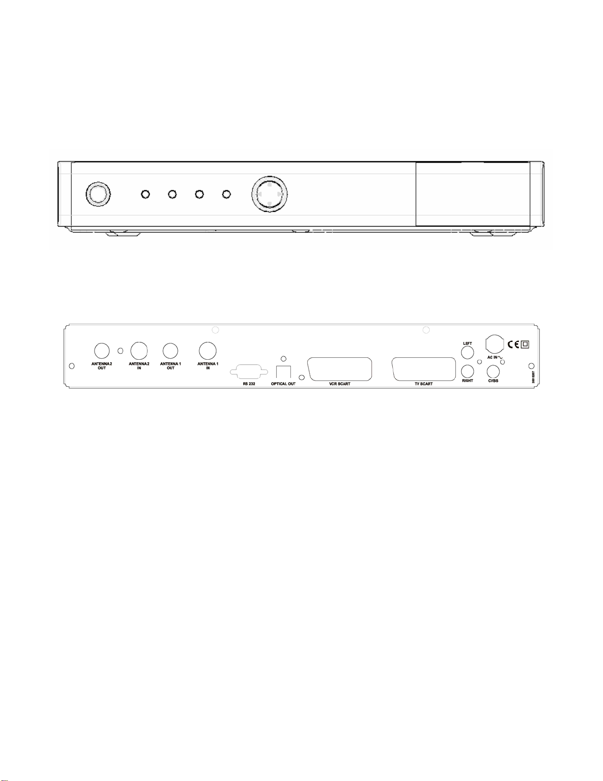
SCART CONNECTION .......................................................................................................................................................... 24
TV S
CART SOCKET
VCR S
CART SOCKET
RS232 S
RCA (A
TECHNICAL SPECIFICATIONS........................................................................................................................................... 26
TROUBLE-SHOOTING ........................................................................................................................................................... 28
PARTS LIST............................................................................................................................................................................... 30
EXPLODED VIEW.................................................................................................................................................................... 31
SCHEMATİCS........................................................................................................................................................................... 32
16PW810-2 POWER BOARD SCHEMATIC.......................................................................................................................... 32
16MB31-1 MAINBOARD SCHEMATIC ............................................................................................................................... 33
16FP38-3 FRONT BOARD SCHEMATIC.............................................................................................................................. 41
16SC31-2 AV SCHEMATIC ................................................................................................................................................... 42
16TUT36-2 TUNER SCHEMATIC ........................................................................................................................................ 44
ERIAL PORT
UDIO AND COMPOSITE VIDEO) CONNECTOR
................................................................................................................................................................... 24
................................................................................................................................................................ 24
................................................................................................................................................................. 25
................................................................................................................ 25
Page 3
Page 4
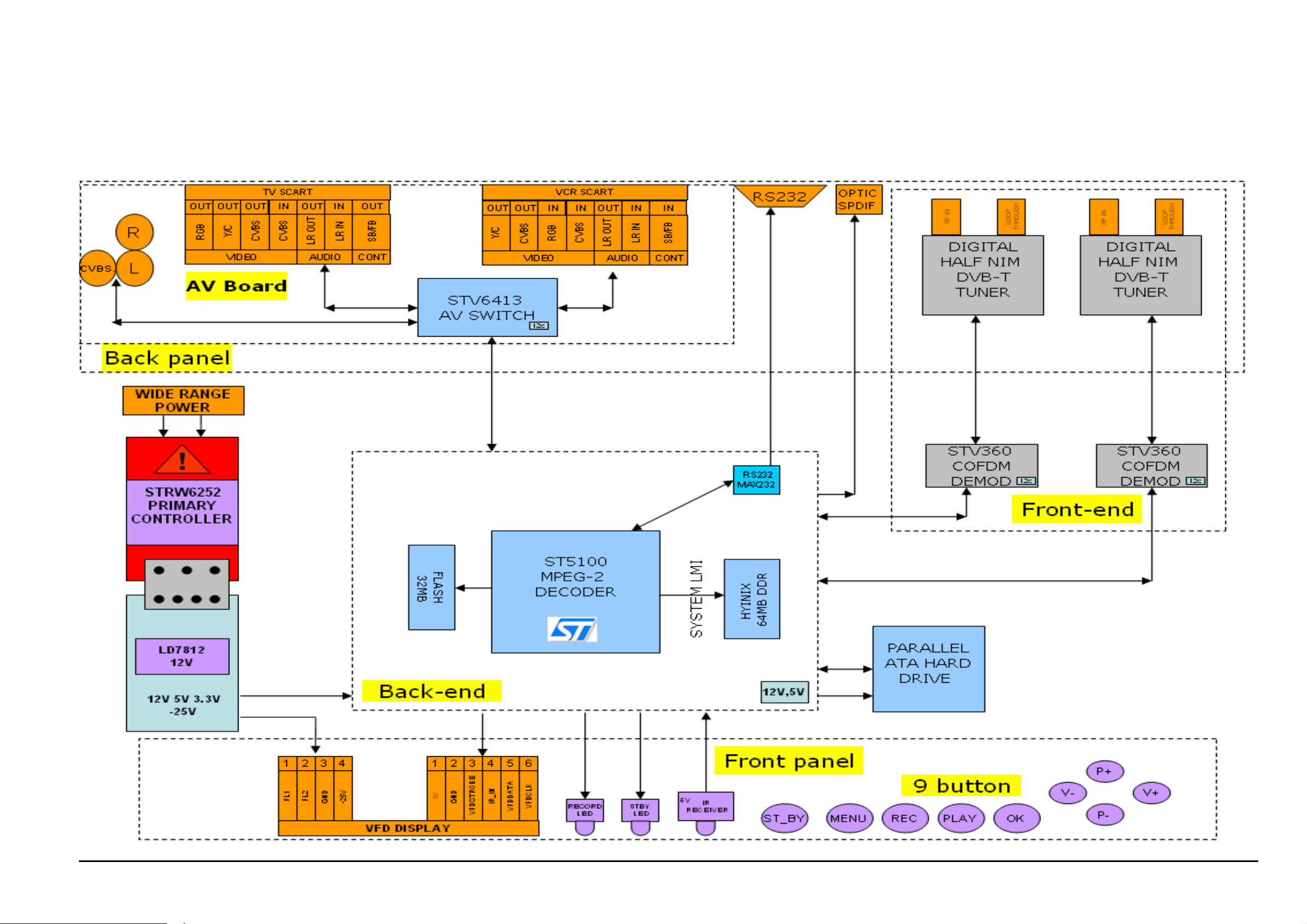
GENERAL DESCRIPTION
Major functional blocks are discussed briefly in this section. A more detailed description is contained later in the document.
BLOCK DIAGRAM
Page 4
Page 5

16mb31-1 Mainboard
STI5100 (IC101)
1. Introduction
The STi5100 is a low-cost Omega2 (The STBus multipath unified interconnect provides high onchip bandwidth and low latency accesses between modules. The interconnect operates hierarchically, with
latency-critical modules placed at the top level. The multipath router allows simultaneous access paths
between modules, and simultaneous read and write phases from different transactions to and from the
modules. Split transactions maximize the use of the available bandwidth.) MPEG device that delivers high
performance and integrates features that provide an overall system cost reduction. The device implements
a fully unified DDR SDRAM based memory architecture and integrates the Omega2 video decoder cell
together with a blitter engine and a multichannel DMA controller to provide enhanced performance for
graphics and real-time stream transfers.
DVR applications are supported by a dual-stream deMUX and using an HDD connected either to
the FMI or USB 2.0 port.The STi5100 includes transport stream routing and strobe decoding logic for
DVB-CI and CableCard (formerly known as POD) modules to reduce implementation cost.
2. Technical Specification
• Features
• Enhanced ST20 32-bit VL-RISC CPU
¾ 243MHz, 8Kbyte ICache, 8Kbyte DCache, 4Kbyte SRAM
• Unified Memory Interface
• Dual Transport Stream Merger
¾ Supports DVB and DIRECTV .
¾ Integrated DES-ECB, DVB and ICAMdescramblers
¾ NDS RASP compliant
¾ Low cost DVB-CI and Cable Card support
• MPEG-2 MP@ML Video Decoder
¾ Trick modes including smooth fast forward andrewind
• Audio
¾ MPEG-1 layers I/II, MP3
¾ Dolby . Digital decoding
¾ Dolby Pro Logic . compatible output
¾ PCM input, mixing and sample rate conversion
¾ SRS/TruSurrondXT . virtual surround sound
¾ Simultaneous MPEG audio decode and outputof Dolby streams
• Graphics/Display
¾ 4 display planes
¾ 2, 4 and 8 bpp CLUT graphics, 256 x 30 bits(AYCBCr) CLUT entries
¾ 16 bpp true color graphics
¾ Alpha blending, antialiasing, antiflutter,antiflicker filters
• PAL/NTSC/SECAM encoder
¾ RGB, CVBS, Y/C and YUV outputs with 10-bitDACs
Page 5
Page 6
SERVICE MANUAL
¾ CGMS, Teletext, WSS, VPS and close caption
• On-Chip Peripherals
¾ 4 ASCs (UARTS)
¾ 4 parallel 8-bit I/O banks
¾ 2 smartcard interfaces and clock generators
¾ 3 SSCs for I²C/SPI master/slave interfaces
¾ Silicon Labs line side (DAA) interface
¾ High-speed USB OHCI/EHCI compliant host interface
¾ DiSEqC interface
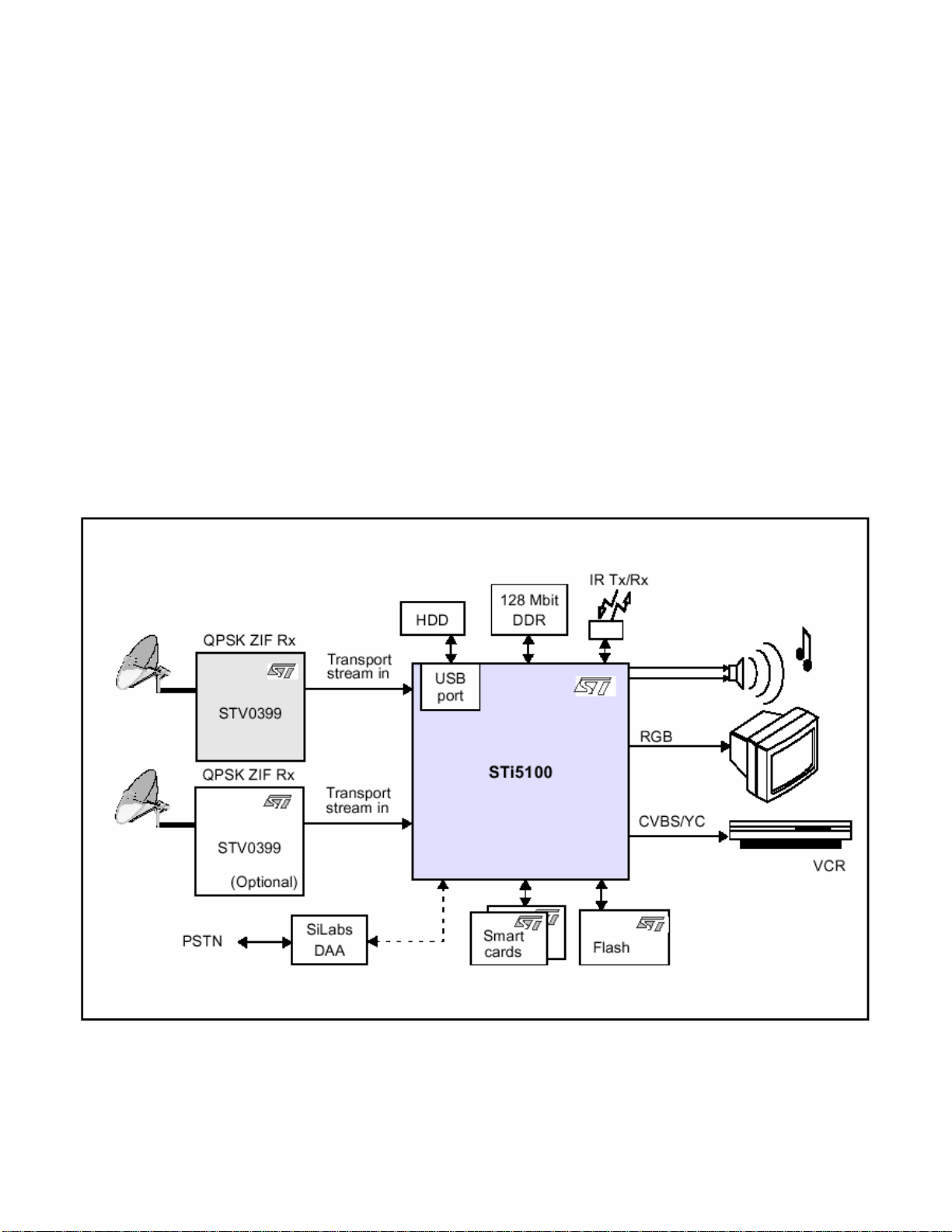
3. Architecture overview
The figure below shows the architecture of the Sti5100.
This chapter gives a brief overview of each of the functional blocks of the STi5100.
4. STi5100 functional modules
4.1 Memory subsystem
Page 6
Page 7

SERVICE MANUAL
The STi5100 has a local memory interface (LMI) and a flash and peripheral interface (FMI). The
STi5100's local memory interface is used for all data requirements in unified memory applications,
including graphics, video and audio buffers. It provides 16-bit wide DDR SDRAM support only at up to
166 MHz. The FMI provides support for 16-bit wide peripherals, flash and synchronous flash.
Local memory interface (LMI)
The LMI is a 16-bit wide DDR SDRAM interface with a peak bandwidth of 664 Mbyte/s (166
MHz). It supports one bank of 128-Mbit, 256-Mbit, or 512-Mbit DDR SDRAM. The LMI provides a fully
cacheable address space for data and instructions, with data cacheability controlled in 512 Kbyte blocks
for up to 8 Mbytes.
Flash and peripheral memory interface (FMI)
The FMI provides a glueless interface to SRAM, flash, SFlash and peripherals, in up to four
configurable banks over a 16-bit wide interface. Bus cycle strobe timings can be programmed from 0 to 15
phases for slower peripherals. The FMI output drive of the STi5100/STi5101 is programmable on a busby-bus basis. Support is provided for connection to an ATAPI HDD.
4.2 Transport stream processing
The STi5100 supports dual independent transport stream inputs using an SRAM-based packet
merger and a single programmable transport interface (PTI). The merger buffers a packet pair per channel.
The incoming transport packets are tagged with a source ID and a time stamp.
Programmable transport interface (PTI)
The PTI performs transport-stream descrambling, demultiplexing and data filtering. PESdata is
transferred by DMA to audio and video decoders using circular buffers. Section data is transferred by
DMA to separate buffers for further processing by the CPU.
• DIRECTV and DVB transport streams can be handled by the PTI with data rates up to 138 Mbit/s.
• The PTI performs PID filtering to select audio, video and data packets to be processed. 96 PID
slots can be supported by the PTI.
• The PTI can descramble streams using the following ciphers:
¾ DES-ECB,
¾ DES-CBC including DVS-042 and cipher text stealing termination block handling,
¾ DVB-CSA,
¾ NDS specific streams can also be supported for integrated ICAM functionality.
• The PTI has a section filter core that filters DVB and DIRECTV standard sections. Four filtering
modes are available:
¾ wide match mode: 48x 16-byte filters,
¾ long match mode: 96x 8-byte filters,
¾ positive/negative mode: 48x 8-byte filters with positive/negative filtering at the bit level.
Matching sections are transferred to memory buffers for processing by software.
When the PTI is required to output a transport stream, it can output the entire transport stream or selected
packets filtered by PID. A latency counter is provided to ensure packet timing is preserved. Packet
substitution can also be performed.
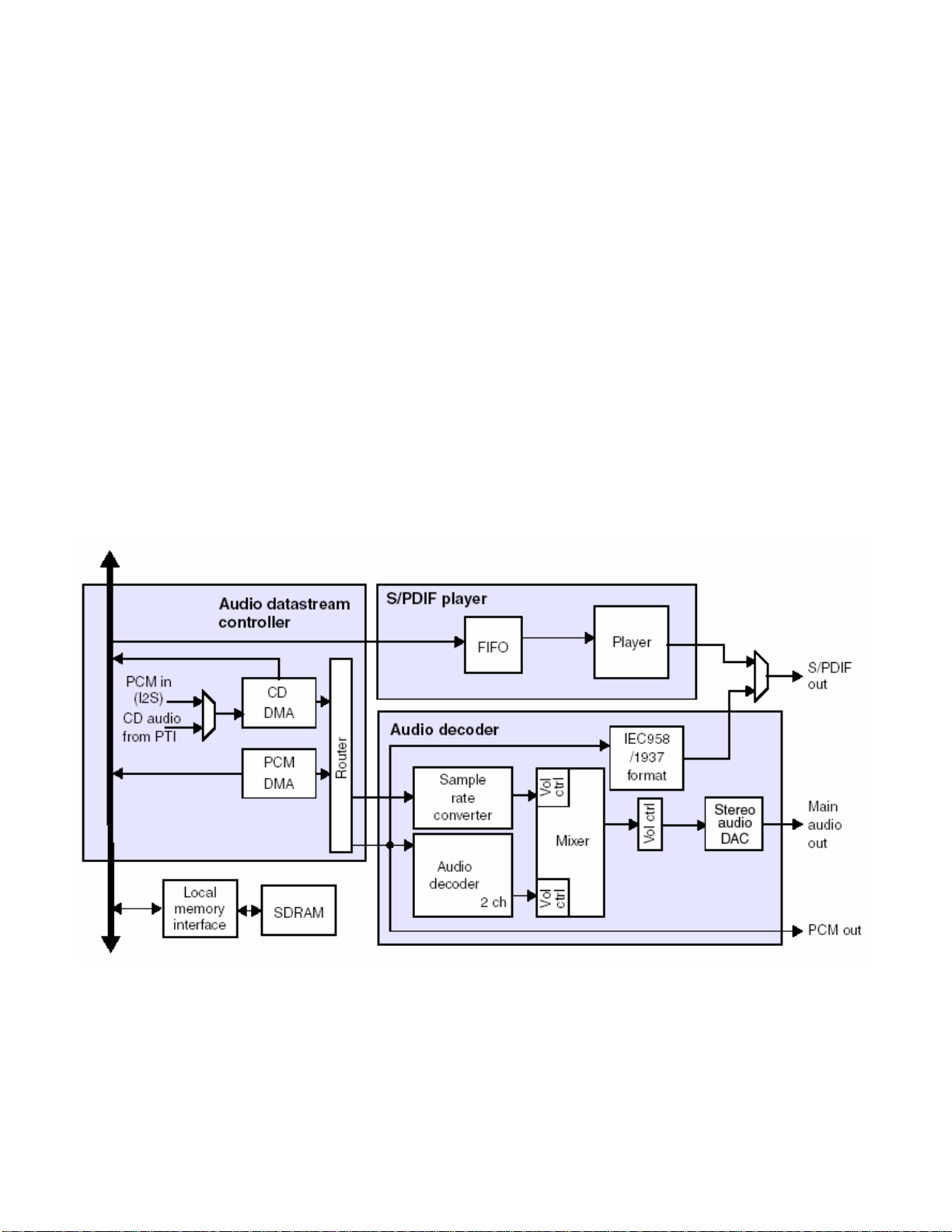
4.3 Audio subsystem
The audio subsystem supports multichannel audio decoding and mixing with internal PCM files.
Decoding of MPEG-1 layers I, II, MP3 and Dolby Digital stereo are supported.Decoded multichannel
Page 7
Page 8
SERVICE MANUAL
audio is downmixed before emerging as stereo or Dolby Pro Logic compatible encoded audio.
Simultaneous MPEG audio decoding and output of Dolby streams on the S/PDIF is also supported. SRS
Labs’ TruSurroundXT is also provided for two speaker virtual surround sound. The integrated DACs
provide analog stereo output directly from the device using a single-ended interface.Multichannel streams
can be passed through to the IEC958 output for external decoding. Audio sample rates of 32 kHz, 44.1
kHz and 48 kHz are supported.The audio digital-to-analog converter is a high performance stereo audio
converter operating at 256 Fs system clock using single-ended voltage. This DAC accepts a 24-bit input
data in I 2 S format from the audio decoder macro block and converts them into up to 2 Vrms output
voltage. Digitized analog audio can also be input to the STi5100 using the PCM input interface and
buffered in memory via DMA. 26/830 STMicroelectronics Confidential 7603604B The audio subsystem
consists of the following units.
¾ Audio datastream controller
The audio datastream controller receives, buffers and reformats audio data. It handles up to three audio
data flows concurrently.
It receives a raw PCM stream from an external source via the PCM input interface or receives a
compressed data stream from an internal source such as the PTI and stores this in a memory buffer via
DMA. This is used to buffer and play the main audio for the digital or analog program.
It receives a PCM file or stream from a memory buffer via DMA and delivers this to the audio decoder’s
second input for sample rate conversion and mixing with the main audio.
The router is able route either source to either input of the audio decoder.
¾ Audio decoder 24-bit audio digital signal processor
The digital signal processor processes audio streams sent to it by the CD player and PCM file player.
¾ S/PDIF player
The independent S/PDIF player can output a compressed Dolby Digital audio stream independently of the
stream being decoded.
Page 8
Page 9

SERVICE MANUAL
¾ IEC958/IEC1937 formatted output
The audio decoder outputs IEC958/IEC1937 formatted CD or PCM audio received from the audio
decoder.
¾ 1-channel PCM output interface
The PCM output interface outputs PCM audio received from the audio decoder.
¾ Integrated 24-bit stereo audio DAC system
¾ Programmable tone generation for dish alignment
4.4 Internal peripherals
The STi5100 has many dedicated internal peripherals for digital TV receiver applications, including:
¾ 2 smartcard controllers,
¾ 4 ASCs (UARTs), two of which are generally used by the smartcard controllers, teletext serializer
and DMA,
¾ 3 SSCs for I 2 C master/slave interfaces, with SPI support,
¾ 4.5 GPIO ports, with a further 1.5 ports mapped to transport pins,
¾ 1 PWM module,
¾ a multichannel, infrared blaster/decoder interface module,
¾ a modem analog front-end interface (MAFE),
¾ DVB common interface support,
¾ CableCard support,
¾ fully integrated digital clock recovery for MPEG (replacement for VCXO),
¾ USB 2.0 host, OHCI/EHCI compliant,
¾ interface to SiLabs line side device (DAA),
¾ an interrupt level controller,
¾ a low-power/RTC/watchdog controller,
¾ DCU toolset support,
¾ a JTAG/TAP interface.
4.5 Clock generation
All system clocks are generated using the clock generator block. This contains two high-frequency PLLs
(600 MHz) that are divided down to produce a series of phase-related programmable clock channels. The
guaranteed phase relationship between these channels simplifies interconnect bridging between different
subsystem modules and gives lower latency compared to a fully asynchronous clocking scheme.
The STi5100 is a clock master. The flash clock output may be phase aligned to optimize the external bus
performance of the FMI.
Digital clock recovery for MPEG (DCO) has been integrated using a special purpose frequency
synthesizer, thus removing the need for an external varactor diode or VCXO module. An external VCXO
can still be used for genlocking applications.
4.6 System clock
External 27 MHz clock
Either a 27 MHz clock can be fed into CLK27IN, or a crystal pi network may be connected between
CLK27IN and CLK27OSC. The crystal option and internal VCO is the option recommended by
STMicroelectronics
.
Page 9
Page 10
SERVICE MANUAL
Page 10
Page 11

SERVICE MANUAL
DDRAM HYNIX 512MBits
The HY5DU12422C(L)TP, HY5DU12822C(L)TP and HY5DU121622C(L)TP are a 536,870,912-bit
CMOS Double Data Rate(DDR) Synchronous DRAM, ideally suited for the main memory applications
which requires large memory density This Hynix 512Mb DDR SDRAMs offer fully synchronous
operations referenced to both rising and falling edges of the clock. While all addresses and control inputs
are latched on the rising edges of the CK (falling edges of the /CK), Data, Data strobes and Write data
masks inputs are sampled on both rising and falling edges of it. The data paths are internally pipelined and
2-bit prefetched to achieve very high bandwidth. All input and output voltage levels are compatible with
SSTL_2.
FEATURES
• VDD, VDDQ = 2.5V ± 0.2V for DDR200, 266, 333
VDD, VDDQ = 2.6V ± 0.1V for DDR400
• All inputs and outputs are compatible with SSTL_2
interface
• Fully differential clock inputs (CK, /CK) operation
• Double data rate interface
• Source synchronous - data transaction aligned to
bidirectional data strobe (DQS)
• x16 device has two bytewide data strobes (UDQS,
LDQS) per each x8 I/O
• Data outputs on DQS edges when read (edged DQ)
Data inputs on DQS centers when write (centered
DQ)
• On chip DLL align DQ and DQS transition with CK
transition
• DM mask write data-in at the both rising and falling
edges of the data strobe
• All addresses and control inputs except data, data
strobes and data masks latched on the rising edges of the clock
• Programmable CAS latency 2/2.5 (DDR200, 266,
333) and 3 (DDR400) supported
• Programmable burst length 2 / 4 / 8 with both
sequential and interleave mode
• Internal four bank operations with single pulsed /RAS
• Auto refresh and self refresh supported
• tRAS lock out function supported
• 8192 refresh cycles / 64ms
Page 11
Page 12

SERVICE MANUAL
HY29LV320 32 Mbit (2M x 16) Low Voltage Flash Memory (IC1)
Low Voltage Single Supply Flash Memory
Single Power Supply Operation
– Read, program and erase operations from 2.7 to 3.6 volts
– Ideal for battery-powered applications
_ High Performance
– 70, 80, 90 and 120 ns access time versions for full voltage range operation
_ Ultra-low Power Consumption (Typical/ Maximum Values)
– Automatic sleep/standby current: 0.5/5.0 µA
– Read current: 9/16 mA (@ 5 MHz)
– Program/erase current: 20/30 mA
_ Top and Bottom Boot Block Versions
– Provide one 8 KW, two 4 KW, one 16 KW and sixty-three 32 KW sectors
_ Secured Sector
– An extra 128-word, factory-lockable sector available for an Electronic Serial Number and/or additional
secured data
_ Sector Protection
– Allows locking of a sector or sectors to prevent program or erase operations within that sector
– Temporary Sector Unprotect allows changes in locked sectors
_ Fast Program and Erase Times (typicals)
– Sector erase time: 0.5 sec per sector
– Chip erase time: 32 sec
– Word program time: 11 µs
– Accelerated program time per word: 7 µs
_ Automatic Erase Algorithm Preprograms and Erases Any Combination of Sectors or the Entire
Chip
_ Automatic Program Algorithm Writes and Verifies Data at Specified Addresses
_ Compliant With Common Flash Memory Interface (CFI) Specification
– Flash device parameters stored directly on the device
– Allows software driver to identify and use a variety of current and future Flash products
_ Minimum 100,000 Write Cycles per Sector
_ Compatible With JEDEC standards
– Pinout and software compatible with single-power supply Flash devices
– Superior inadvertent write protection
_ Data# Polling and Toggle Bits
– Provide software confirmation of completion of program and erase operations
_ Ready/Busy (RY/BY#) Pin
– Provides hardware confirmation of completion of program and erase operations
_ Write Protect Function (WP#/ACC pin)
- Allows hardware protection of the first or last 32 KW of the array, regardless of sector protect status
_ Acceleration Function (WP#/ACC pin)
- Provides accelerated program times
_ Erase Suspend/Erase Resume
– Suspends an erase operation to allow reading data from, or programming data to, a sector that is not
being erased
Page 12
Page 13

SERVICE MANUAL
– Erase Resume can then be invoked to complete suspended erasure
_ Hardware Reset Pin (RESET#) Resets the Device to Reading Array Data
_ Space Efficient Packaging
– 48-pin TSOP and 63-ball FBGA packages
16tut36-2 tuner board
STV0360/0361(COFDM demodulators IC for terrestrial TV set-top box)
STMicroelectronics complements the world leading range of MPEG-2 decoders with a range of COFDM
demodulators for digital terrestrial applications. The STV0360 and STV0361 demodulators are high
performance COFDM (Coded Orthogonal Frequency Division Multiplex) demodulators with built in A/D
converters. They perform all the demodulation functions to extract the MPEG-2 transport stream from the
tuner input.
• DVB-T (ETS 300 744), NORDIG II and NORDIG Unified 1.0.1 compliant1
• Inputs for direct IF, eliminating the need for a down-converter in the tuner
• Adaptative channel correction in both time and frequency, providing excellent performance, event
in the presence of noise or significant Doppler shift.
• Dual Automatic Gain Controller (AGC) to seamlessly interface with all tuners characteristics
• Support for 2K/8K carrier detection modes
• PGA (Programmable Gain Amplifier) increasing flexibility to enhance tuner power matching
• Additional A/D converter to directly monitor the input level of the new generation of tuners
Page 13
Page 14
SERVICE MANUAL
Page 14
Page 15

SERVICE MANUAL
TUNER (DTOS449IV241B-DTOS443PV241B)
DESCRIPTION
Page 15
Page 16

SERVICE MANUAL
ELECTRICAL CHARACTERISTICS
Page 16
Page 17

SERVICE MANUAL
16sc31-2 scart board
STV6414Audıo/Vıdeo Switch Matrix(IC200)
• I²C Bus Control
• Standby Mode with Interrupt Signal Output
• Video Section
• 3 CVBS Inputs, 2 CVBS Outputs
• 3 Y/C Inputs, 2 Y/C Outputs
• 6dB Gain on all CVBS/Y and C Outputs
• Integrated 150W Buffers
• 2 RGB/FB Inputs, 1 Tri-state RGB/FB Output with 6dB Adjustable Gain (from +3dB to +9dB)
• Video Muting on all Outputs
• 2 Slow Blanking Inputs/Outputs
• Sync Bottom Clamp on all CVBS/Y and RGB
• Inputs, Average Clamp on C Inputs
• Bandwidth: 15MHz
• Crosstalk: 50dB Minimum
• Audio Section
• 3 Stereo Inputs, 3 Stereo Outputs
• Stereo-to-Mono Sound Capability
• 0/6/9dB Selectable Gain on one Stereo Input
• Full Range Volume Control with Soft Control
Audio Muting on all Outputs
•
Thermal Data :
Page 17
Page 18

SERVICE MANUAL
16PW810-2 Power board
16MB07 E3 Board
Power Consumption
Voltage Current mA Power
Watts
11.7W
+12V
STAND_BY
POWER_ON
The Sanken concept is used for power supply. Sanken SRTW6252 is designed. The receiver
works between 85 and 265 VAC mains voltage by using STRW6252 .In SMPS applications, secondary
voltage regulation is adjusted according to the feedback voltage from the secondary side of transformer.
The feedback voltages are 3.3V and 5V. This is connected to the comparator pin of STRW6252 via IC2
(Optocoupler). The comparator pin also protects the box against short circuits and overload. The supply
voltage of STRW6252 is between 8.9V 17V at pin4.
+5V
+3V3 ----
Voltage Current mA Power
Watts
19W
+12V
+5V
+3V3
Page 18
Page 19

SERVICE MANUAL
Controller Electrical characteristics:
Output voltages of the transformer (TR2):
(i) 3.3V: 5100 IC (IC101),flash memory (IC 1), tuner and other components.
(ii) 5V: Front panel board, Tuner , and some ICs and circuits.
(iii) 12V: hard disk and some other ic and circuits
(iv) -25V :flaman voltage
16fp38-3 front board
VFD Driver/Controller IC PT6311(IC2)
• CMOS Technology
• Low Power Consumption
• Key Scanning (12 x 4 matrix)
• Multiple Display Modes: (12 segments, 16 digits to 20 segments, 8 digits)
• 8-Step Dimming Circuitry
• LED Ports Provide (5 channels, 20 mA max.)
• 4- Bits General Purpose Input Ports Provided
• Serial Interface for Clock, Data Input, Data Output, Strobe Pins
• No External Resistors Needed for Driver Outputs
Page 19
Page 20

SERVICE MANUAL
Front board connector – PL5
Pin Description
1 +12VSTB
2 GND
3 GND
4 +5VSTB
Front board Connector – PL811
Pin Description
1 +5V
2 GND
3 S ENSE
4 IR_IN
5 DISP DATA
6 DISP CLK
Page 20
Page 21

SERVICE MANUAL
VACUUM FLUORESCENT DISPLAY
Page 21
Page 22

SERVICE MANUAL
USED IC LISTS
MAINBOARD ( B )16M 31-1
Sti5100 (IC101) Set Top Box Backend Decoder with Integrated Host Processor
MAX232 (IC601) RS232 Driver / Rec
74LVC244 (IC878) IC 3-ST BUFFER
74LVX00 (IC902) Low Voltage Quad 2-Input NAND
74LVT14 (IC903) 3.3V Hex inverter Schmitt trigger
74LVTH244A ( ) Low Voltage Octal Buffe
IC900 r/Line Driver
FLASH (IC1) 32MBIT 3.3V ROHS
74LVTH16245A (IC901) Low Voltage 16-Bit
LM1117 ( IC500 ,IC473) LDO 1.8V/80
LDO (DPAK) (IC606) 1.2V/800mA
REG LM7808 8V/1A (IC102) 1A REGULATORS
DDRAM(IC2)
POWER BOARD 6 0
STRW-6252 (IC1 SMPS primary
(1 PW81 -2)
) IC
SFH617A (IC2) Optocoupler
TL431(IC3) Programmable Precision Refere
LM7812 (IC5)
SCART BOARD (16SC31-2)
FRONT BOARD (16FP38-3)
VFD Driver/Controller IC PT6311(IC2)
eiver
Gate
Transceiver with 3-STATE Outputs
0mA
IC DDRRAM32MX16
nce
12V Voltage Regulator
WITCH A/V STV6414 (IC200) IC S
Page 22
Page 23

SERVICE MANUAL
CONNECTORS
Power L451 Connector – P
Pin Description
1 +12V
2 GND
3 GND
4 5V
5 +3V3
6 +3V3
7 STBY
8 NC
9 NC
Fr t Panel Conne PL609 on ctor –
Pin De n scriptio
1 +5V
2 GND
3 SENSE
4 IR_IN
5 DISP DATA
6 DISP CLK
Hard disk pow 04 er – PL4
Pin De n scriptio
1 +12VSTB
2 GND
3 GND
4 +5VSTB
Fan power – PL450
Pin Description
1 NC
2 +5V
3 GND
Pin De n scriptio Pin De scription
1 HDDRESET 21 GND
2 GND 22 GND
3 HBUFDATA7 23 H_DIOW
4 HBUFDATA8 24 GND
5 HBUFDATA6 25 H_DIOR
6 HBUFDATA9 26 GND
7 HBUFDATA5 27 IORDY
8 HBUFDATA10 28
9 HBUFDATA4 29
10 HBUFDATA11 30 GND
11 HBUFDATA3 31 HDD-IRQ
12 HBUFDATA12 32 NC
13 HBUFDATA2 33 DA1
14 HBUFDATA13 34 GND
15 HBUFDATA1 35 DA0
16 HBUFDATA14 36 DA2
17 HBU A0 FDAT 37 HDDCS-0
18 HBUF A15 38 HDDCS-1 DAT
19 GND 39 IDE-DASP
20 NC 40 GND
H a Conne r – PL900 ard disk dat cto
AV Connector – PL340
Pin De n scriptio Pin Description
1 +12V 11 C
2 GND 12 FBOUTENC
3 +5V 13 AV_INT
4 GND 14 GND
5 Red 15 LEFT AUDIO
6 Green 16 RIGHT IO AUD
7 Blue 17 GND
8 G ND 18 GND
9 CVBS 19 SDA0
10 Y 20 SCL0
Page 23
Page 24

SERVICE MANUAL
SCART CONNECTION
20 18 16 14 12 10 8 6 4 2
21 19 17 15 13 11 9 7 5 3 1
TV Scart Socket
TV Scart Sock PL1et – 01
Pin Description Pin Description
1
2
3
4
5
6
7
8
9
10
11
Audio Right Output nnection
No Connection
Audio Left Output
GND
GND
No Connection
BLUE Output
Function Switching Output
GND
No Connection
GREEN Outp
ut
12
13
14
15
16
17
18
19
20
21
No Co
GND
GND
RED Output
Fast Blanking Output
GND
GND
CVBS Output
No Connection
GND
VCR Scart Socket
VCR Scart Sock PL1et - 00
Pin Description Pin Description
1
Audio
Right
Output
12 No Co
nnection
2 Audio Right Input 13 GND
3 Audio Left Output 14 GND
4 GND 15 No Connection
5 GND 16 No Connection
6 Audio Left Input 17 GND
7 No Connection 18 GND
8 Function Switching Input t 19 CVBS Outpu
9 GND 20 CVBS Input
10 No Connection 21 GND
11 No Connection
Page 24
Page 25

SERVICE MANUAL
RS232 Serial Port
RS232 Header – J SUB_9K_D
Pin Description Pin Description
1 - 2 3 TXD 4 CTS
5 R RTS XD 6
7 - 8 9 GND
RCA (Audio and Composite Video) Connector
A/V Connector – JK1
Pin Description
1 RIGHT AUDIO
2 LEFT AUDIO
3 SPDIF AUDIO
Page 25
Page 26

SERVICE MANUAL
TECHNICAL SPECIFICATIONS
GENERAL CHARACT R
Supply Voltage 220 - 240 V AC ~ 50Hz
Input Frequency 470Mhz-862Mhz
Maximum Power consumption 20W
Operating temperature ºC to +40ºC 5
Storage temperature -15ºC to +55ºC
Humidity 25 to 75% rel
Physical dimensions 360x280x48 mm
Weight 2820 g
HARDWARE CONFIGURATION
Main Processor STi5100
Flash Memory MB 4
DDRAM 2 MB 3
DIGITAL CAPABILITIES
Transmission Standards VB, MPEG2 D
DEMODULATION
COFDM with 2K/8K FFT mode.
FEC for all DVB Modes.(Automatically found)
VIDEO
ALL MPEG-2 MP@ML Video Decoder
Aspect Ratio 4:3, 16:9 with pan vector
RGB analogue outputs. BW ≥ 5MHz at 0.5 to 5MHz sweep signal
E ISTICS
CVBS analogue output.
AUDIO
MPEG1 Layer 1 and 2
Sampling frequencies supported 32kHz, 44.1kHz, or 48kHz.
Output can be programmed as STEREO, LEFT
o
nly or RIGHT only (on both outputs). This is
u
seful for dual mono channels in order to select
th
e correct sound track, which is stored for every
c
hannel.
Wide dynamic range 16-bit resolution
Page 26
Page 27

SERVICE MANUAL
REMOTE RO CONT L
Operating Distance 10m Max.
Batteries 2x1.5V Micro (R-03/AAA)
TUNERS
2 xRF In : IEC-type, female (75Ohm)
2 x RF Out (loop through) : C-type, male (75Ohm) IE
FRONT PANEL
Display VFD
Remote Control Keys tandby ON/OFF,Record,Play, Menu, OK,PR+ /
1 Slot CI (Opt.), 1 Slot Smart Card (Opt.),USB2.0
AUDIO R / L
Connector x RCA (R + L) 2
Output .5 Vrms dBfs / Z = 1 kohm 0
DIGITAL AUDIO
Output Optik SPDIF
A / V & DATA IN / O UT
Scart TV scart, VCR scart
RGB Video Output TV scart
RGB Video Intput VCR scart
CVBS Video Output TV scart, VCR scart
CVBS Video Input CR scart V
Analog Audio Output V scart, RCA jack , VCR scart T
Analog Audio Input VCR scart
Digital Audio Output Optic output
Data Interface
S
P
R-, V+ / V -,Standby Led, Record Led,
connector (Opt.)
Scart RS 232, RS232 (max 115200 bps),9Pin
Page 27
Page 28

SERVICE MANUAL
TROUBLE-SHOOTING
FAULTY SUPPLY/
DO NOT OPEN/
DO NOT INIT
) Control the 3,3V,5V,12, supply voltages from the PL451 connector
1
)Control the frequency of the 27MHz X25 crystal.
2
3)Control the frequency of the 133Mhz from the S11
6 point.
) Control the IC600 RESET IC 5V supply voltage .After power on the
4
device , RESET IC output must be high in 200ms.
.2V must be seen on the C600 reset pin.
1
5)Control the R187 , R188 , R189, R195 I2C lines.
)Control the HDD , remove the HDD power cable and control if there is
6
a Sc or not on the HDD .The resistor value between 5V to GND is near
4Kohm.
)Control that all cables are connected between the boards.(AVcable,
7
power cable ,HDD data cable
)
ly
NO VIDEO/
BAD VIDEO IMAGE
NO A DIO/
U
BAD AUDIO&
PARASITIC
) Control the TV scart pins.
1
2) Control the IC200 supply voltages and SDA&SCL lines.
3) Control the video signals on the PL200& PL304 connectors.
)Control all audio output from the SCART AUDIO OUTPUTS.
1
)Control the IC200 supply voltages and SDA&SCL lines.
2
3) Contol the
capacitors C226& C227 on the Av board.
4
) Control the signal from the point of C143 C144 capasitors on the
mainboard.
5) Control dc signal on the C143 C144 capasitors on the mainboard.
Page 28
Page 29

SERVICE MANUAL
DISPLAY ERROR
OSD ERROR
CRASH&SW LOCKED
AV Switching ERROR
HARDDISK ERROR
1)Control the 3.3V , VFDDATA&DISPCLK signals on the PL 453.
2) Control the transistors Q410 ,Q404 ,Q403 around the PL610 connector.
3) Control the IC2 on the front board.
1) Control the sections that are written in the first part.
1) There may be a SW error. Load the sw again.
2) Control the X100 crystal.
3)Push the standby button for a few seconds.
1) Control the IC200 supply voltages and SDA&SCL lines.
1) Control the HDD 12V & 5V supply voltages from the HDD power
connektor.
2) Control the HDD , remove the HDD power cable and control if
there is a Sc or not on the HDD .The resistor value between 5V to
GND is nearly 4Kohm.Control the HDD data cable.
3) Use FTI and HDD format options on the SW menu to reset HDD.
Page 29
Page 30

THE UPDATED PARTS LIST
FOR THIS MODEL IS
AVAILABLE ON ESTA
Page 30
Page 31

PVR1000
EXPLODED DIAGRAM
Page 31
Page 32

16PW810-2
POWER BOARD
Page 32
Page 33

16MB31-1
MAIN BOARD - SHEET 1 of 8
Page 33
Page 34

16MB31-1
MAIN BOARD - SHEET 2 of 8
Page 34
Page 35

16MB31-1
MAIN BOARD - SHEET 3 of 8
Page 35
Page 36

16MB31-1
MAIN BOARD - SHEET 4 of 8
Page 36
Page 37

16MB31-1
MAIN BOARD - SHEET 5 of 8
Page 37
Page 38

16MB31-1
MAIN BOARD - SHEET 6 of 8
Page 38
Page 39

16MB31-1
MAIN BOARD - SHEET 7 of 8
Page 39
Page 40

16MB31-1
MAIN BOARD - SHEET 8 of 8
Page 40
Page 41

16FP38-3
FRONT BOARD
Page 41
Page 42

16SC31-2
AV BOARD - SHEET 1 of 2
Page 42
Page 43

16SC31-2
AV BOARD - SHEET 2 of 2
Page 43
Page 44

16TUT36-2
TUNER BOARD
Page 44
Page 45

Hitachi, Ltd. Tokyo, Japan
International Sales Division
THE HITACHI ATAGO BUILDING,
No. 15 –12 Nishi Shinbashi, 2 – Chome,
Minato – Ku, Tokyo 105-8430, Japan.
HITACHI EUROPE LTD,
Whitebrook Park
Lower Cookham Road
Maidenhead
Berkshire
SL6 8YA
UNITED KINGDOM
Tel: 01628 643000
Fax: 01628 643400
Email: consumer-service@hitachi-eu.com
HITACHI EUROPE GmbH
Munich Office
Dornacher Strasse 3
D-85622 Feldkirchen bei München
GERMANY
Tel: +49-89-991 80-0
Fax: +49-89-991 80-224
Hotline: +49-180-551 25 51 (12ct/min)
Email: HSE- DUS.service@hitachi-eu.com
HITACHI EUROPE srl
Via Tommaso Gulli N.39, 20147
Milano, Italia
ITALY
Tel: +39 02 487861
Tel: +39 02 38073415 Servizio Clienti
Fax: +39 02 48786381/2
Email: customerservice.italy@hitachi-eu.com
HITACHI EUROPE S.A.S
Lyon Office
B.P. 45, 69671 BRON CEDEX
FRANCE
Tel: +33 04 72 14 29 70
Fax: +33 04 72 14 29 99
Email: france.consommateur@hitachi-eu.com
HITACH EUROPE AB
Egebækgård
Egebækvej 98
DK-2850 Nærum
DENMARK
Tel: +45 43 43 6050
Fax: +45 43 60 51
Email: csgnor@hitachi-eu.com
Hitachi Europe Ltd
Bergensesteenweg 421
1600 Sint-Pieters-Leeuw
BELGIUM
Tel: +32 2 363 99 01
Fax: +32 2 363 99 00
Email: sofie.van.bom@hitachi-eu.com
www.hitachidigitalmedia.com
Tel: 03 35022111
HITACHI EUROPE S.A.
364 Kifissias Ave. & 1, Delfon Str.
152 33 Chalandri
Athens
GREECE
Tel: 1-6837200
Fax: 1-6835964
Email: service.hellas@hitachi-eu.com
HITACHI EUROPE S.A.
Gran Via Carlos III, 86, planta 5
Edificios Trade - Torre Este
08028 Barcelona
SPAIN
Tel: +34 93 409 2550
Fax: +34 93 491 3513
Email: atencion.cliente@hitachi-eu.com
HITACHI Europe AB
Box 77 S-164 94 Kista
SWEDEN
Tel: +46 (0) 8 562 711 00
Fax: +46 (0) 8 562 711 13
Email: csgswe@hitachi-eu.com
HITACHI EUROPE LTD (Norway) AB
STRANDVEIEN 18
1366 Lysaker
NORWAY
Tel: 67 5190 30
Fax: 67 5190 32
Email: csgnor@hitachi-eu.com
HITACHI EUROPE AB
Neopoli / Niemenkatu 73
FIN-15140 Lahti
FINLAND
Tel : +358 3 8858 271
Fax: +358 3 8858 272
Email: csgnor@hitachi-eu.com
HITACHI EUROPE LTD
Na Sychrove 975/8
101 27 Pr aha 10 – Bohdalec
CZECH REPUBLIC
Tel: +420 267 212 383
Fax: +420 267 212 385
Email: csgnor@hitachi-eu.com
 Loading...