

Page 1
查询HA178L00供应商
Description
The HA178L00 series three-terminal fixed output voltage regulators. Can be used not only as stabilized
power sources, but also as Zener diodes because of their small outline package.
HA178L00 Series
3-terminal Fixed Voltage Regulators
Features
• Maximum output current: 150 mA (Tj= 25°C)
• Large maximum power dissipation: 800 mW
• Overcurrent protection
• Temperature protection circuit
Ordering Information
Standard Output Voltage
Application
Industrial use HA178L00P HA178L00PA
Commercial use HA178L00 HA178L00A
Tolerance ±8%
A Version Output Voltage
Tolerance ±5%
HA178L00UA
Page 2
HA178L00 Series
Output Voltage and Type
HA178L00PA • HA178L00P • HA178L00A • HA178L00
Output Voltage (V) Type Package
2.5 HA178L02 TO-92M
5 HA178L05
5.6 HA178L56
6 HA178L06
8 HA178L08
9 HA178L09
10 HA178L10
12 HA178L12
15 HA178L15
HA178L00UA
Output Voltage (V) Type Marking Package
2.5 HA178L02UA 8A UPAK
5 HA178L05UA 8B
5.6 HA178L56UA 8C
6 HA178L06UA 8D
8 HA178L08UA 8E
9 HA178L09UA 8F
10 HA178L10UA 8G
12 HA178L12UA 8H
15 HA178L15UA 8J
2
Page 3

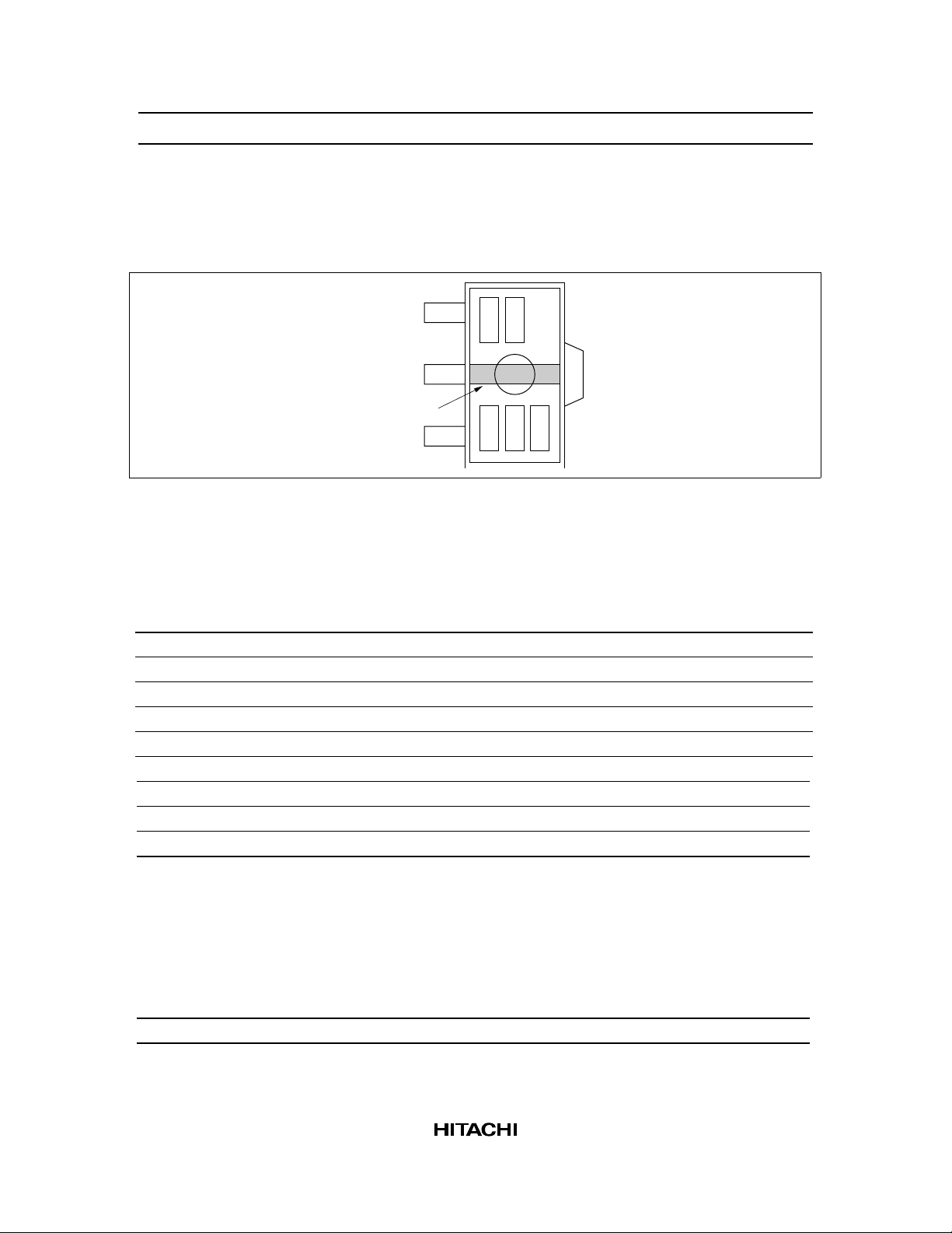
Pin Arrangement
HA178L00 Series
••
UPAKTO-92M
4
MarkMark
1. OUT
2. GND
1
2
3
3. IN
123
1. OUT
2. GND
3. IN
4. GND
Block Diagram
(3) IN
Over Current
Protection
Standard Circuit
Error
Amp.
Temperature
Protection
IN OUT
C
IN
HA178Lxx
V
IN
0.33µF 0.1µF
Vref = 2.5 V
Reference
Voltage
C
OUT
(1) OUT
(2) GND
V
OUT
3
Page 4
HA178L00 Series
UPAK Product (HA178L00UA) Mark Patterns
The mark patterns shown below are used. on UPAK products, as the package is small. Note that the product
code and mark pattern are different.The pattern is laser-printed.
OUT
(1) (2)
GND
Band Mark
IN
Notes: 1. Boxes (1) to (5) in the figures show the position of the letters or numerals, and are not actually
marked on the package.
2. (1) and (2) show the product-specific mark pattern. (see table 1)
Table 1
(3) (4) (5)
Output Voltage (V) Product No. Mark Pattern (2 digit)
2.5 HA178L02UA 8A
5 HA178L05UA 8B
5.6 HA178L56UA 8C
6 HA178L06UA 8D
8 HA178L08UA 8E
9 HA178L09UA 8F
10 HA178L10UA 8G
12 HA178L12UA 8H
15 HA178L15UA 8J
3. (3) shows the production year code (the last digit of the year).
4. (4) shows the production month code (see table 2).
Table 2
Production Month 1 23456789101112
Marked Code A B C D E F G H J K L M
5. (5) shows the production week code.
4
Page 5
HA178L00 Series
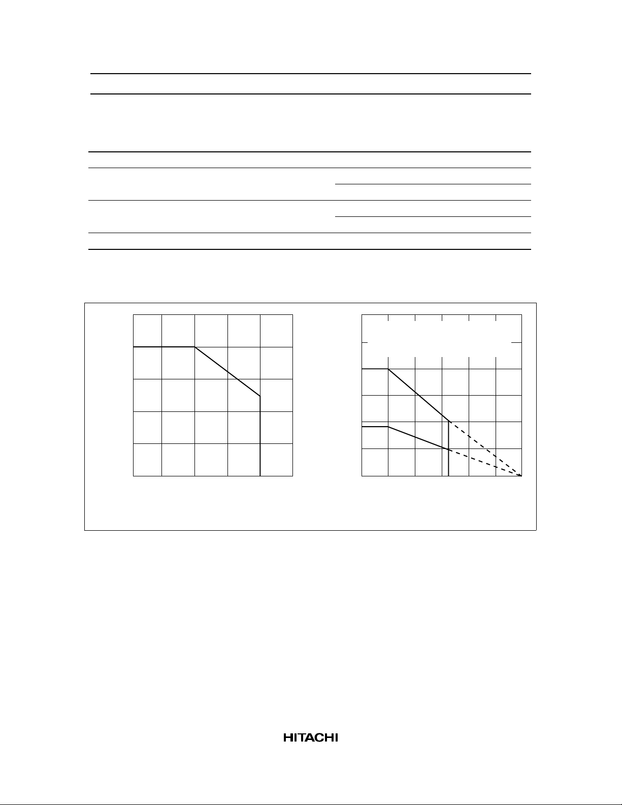
Absolute Maximum Ratings (Ta = 25°C)
Item Symbol Rating Unit Note
Input voltage V
Power dissipation P
IN
T
Operating ambient temperature Topr –20 to +75 °C TO-92M
Storage temperature Tstg –55 to +150 °C
Note: 1. Ta ≤ 25°C, If Ta >25°C, derate by 6.4 mW/°C (See figure A)
2. 15mm × 25mm × 0.7 mm alumina ceramic board, Ta ≤ 25°C (See figure B)
35 V
800 mW TO-92M*
800 mW UPAK*
–20 to +85 °C UPAK
1
2
1,000
(mW)
T
800
600
400
200
Maximum Power Dissipation P
0
–20 0 25 50 75 100
Ambient Temperature Ta (°C)
AB
480
1,200
(1) Non Board
(mW)
1,000
T
(2) 15mm × 25mm × 0.7mm
Alumina Ceramic Board
800
600
(2)
400
(1)
200
Maximum Power Dissipation P
0
25 50 12575 150
Ambient Temperature Ta (°C)
100
5
Page 6
HA178L00 Series
HA178L02 Electrical Characteristics
(VIN = 10 V, I
Item Symbol Min Typ Max Min Typ Max Unit Test Conditions
Output voltage V
Line regulation δV
Load regulation δV
Output voltage V
Quiescent
current
Quiescent δI
current change
Ripple rejection
ratio
Temperature
coefficient of
output voltage
= 40 mA, 0°C Tj 125°C, CIN = 0.33 µF, C
OUT
HA178L02PA
OUT
OLINE
HA178L02P
HA178L02
2.32 2.48 2.64 2.38 2.48 2.58 V Tj = 25°C
— 35 125 — 35 95 mV Tj = 25°C 7 V ≤ VIN ≤ 20 V
HA178L02A
HA178L02UA
— 30 100 — 30 75 8 V ≤ VIN ≤ 20 V
OLOAD
— 14 — — 14 — mV Tj = 25°C 1.0 mA ≤ I
— 9.5 50 — 9.5 50 1.0 mA ≤ I
— 4.5 25 — 4.5 25 1.0 mA ≤ I
OUT
2.28 — 2.68 2.35 — 2.61 V 7 V ≤ VIN ≤ 20 V,
2.28 — 2.68 2.35 — 2.61 VIN = 9 V, 1.0 mA ≤ I
I
Q
Q
— 3.0 6.0 — 3.0 6.0 mA Tj= 25°C
— — 1.5 — — 1.5 mA Tj= 25°C 8 V ≤ VIN ≤ 20 V
— — 0.2 — — 0.1 1.0 mA ≤ I
R
δV
REJ
OUT
— 60 — — 60 — dB f = 120 Hz,
/δTj — +0.2 — — +0.2 — mV/°CI
= 0.1 µF)
OUT
1.0 mA ≤ I
8.0 V ≤ V
= 5 mA
OUT
≤ 40 mA
OUT
< 18 V, Tj = 25°C
IN
≤ 150 mA
OUT
≤ 100 mA
OUT
≤ 40 mA
OUT
≤ 70 mA
OUT
≤ 40 mA
OUT
6
Page 7
HA178L00 Series
HA178L05 Electrical Characteristics
(VIN = 10 V, I
Item Symbol Min Typ Max Min Typ Max Unit Test Conditions
Output voltage V
Line regulation δV
Load regulation δV
Output voltage V
Quiescent
current
Quiescent δI
current change
Ripple rejection
ratio
Temperature
coefficient of
output voltage
Dropout voltage V
= 40 mA, 0°C Tj 125°C, CIN = 0.33 µF, C
OUT
HA178L05PA
OUT
OLINE
HA178L05P
HA178L05
4.68 5.0 5.32 4.8 5.0 5.2 V Tj = 25°C
— 55 200 — 55 150 mV Tj = 25°C 7 V ≤ VIN ≤ 20 V
HA178L05A
HA178L05UA
— 45 150 — 45 100 8 V ≤ VIN ≤ 20 V
OLOAD
— 16 — — 16 — mV Tj = 25°C 1.0 mA ≤ I
— 11 60 — 11 60 1.0 mA ≤ I
— 5.0 30 — 5.0 30 1.0 mA ≤ I
OUT
4.6 — 5.4 4.75 — 5.25 V 7 V ≤ VIN ≤ 20 V,
4.6 — 5.4 4.75 — 5.25 VIN = 10 V, 1.0 mA ≤ I
I
Q
Q
— 3.0 6.0 — 3.0 6.0 mA Tj = 25°C
— — 1.5 — — 1.5 mA Tj = 25°C 8.0 V ≤ VIN ≤ 20 V
— — 0.2 — — 0.1 1.0 mA ≤ I
R
δV
REJ
OUT
DROP
— 58 — — 58 — dB f = 120 Hz,
/δTj — +0.1 — — +0.1 — mV/°CI
— 1.7 — — 1.7 — V Tj = 25°C
= 0.1 µF)
OUT
1.0 mA ≤ I
8.0 V ≤ V
= 5 mA
OUT
≤ 40 mA
OUT
< 18 V, Tj = 25°C
IN
≤ 150 mA
OUT
≤ 100 mA
OUT
≤ 40 mA
OUT
≤ 70 mA
OUT
≤ 40 mA
OUT
7
Page 8

HA178L00 Series
HA178L56 Electrical Characteristics
(VIN = 11 V, I
Item Symbol Min Typ Max Min Typ Max Unit Test Conditions
Output voltage V
Line regulation δV
Load regulation δV
Output voltage V
Quiescent
current
Quiescent δI
current change
Ripple rejection
ratio
Temperature
coefficient of
output voltage
Dropout voltage V
= 40 mA, 0°C Tj 125°C, CIN = 0.33 µF, C
OUT
HA178L56PA
OUT
OLINE
HA178L56P
HA178L56
5.24 5.6 5.96 5.38 5.6 5.82 V Tj = 25°C
— 50 200 — 50 150 mV Tj = 25°C 7.6 V ≤ VIN ≤ 21 V
HA178L56A
HA178L56UA
— 45 150 — 45 100 8.5 V ≤ VIN ≤ 21 V
OLOAD
— 17 — — 17 — mV Tj = 25°C 1.0 mA ≤ I
— 11 60 — 11 60 1.0 mA ≤ I
— 5.0 30 — 5.0 30 1.0 mA ≤ I
OUT
5.16 — 6.04 5.32 — 5.88 V 7.6 V ≤ VIN ≤ 21 V,
5.16 — 6.04 5.32 — 5.88 VIN = 11 V, 1.0 mA ≤ I
I
Q
Q
— 3.0 6.0 — 3.0 6.0 mA Tj = 25°C
— — 1.5 — — 1.5 mA Tj = 25°C 8.5 V ≤ VIN ≤ 2.0 V
— — 0.2 — — 0.1 1.0 mA ≤ I
R
δV
REJ
OUT
DROP
— 58 — — 58 — dB f = 120 Hz,
/δTj — +0.1 — — +0.1 — mV/°CI
— 1.7 — — 1.7 — V Tj = 25°C
= 0.1 µF)
OUT
1.0 mA ≤ I
8.5 V ≤ V
= 5 mA
OUT
≤ 40 mA
OUT
< 18.5 V, Tj = 25°C
IN
≤ 150 mA
OUT
≤ 100 mA
OUT
≤ 40 mA
OUT
≤ 70 mA
OUT
≤ 40 mA
OUT
8
Page 9

HA178L00 Series
HA178L06 Electrical Characteristics
(VIN = 11 V, I
Item Symbol Min Typ Max Min Typ Max Unit Test Conditions
Output voltage V
Line regulation δV
Load regulation δV
Output voltage V
Quiescent
current
Quiescent δI
current change
Ripple rejection
ratio
Temperature
coefficient of
output voltage
Dropout voltage V
= 40 mA, 0°C Tj 125°C, CIN = 0.33 µF, C
OUT
HA178L06PA
OUT
OLINE
HA178L06P
HA178L06
5.61 6.0 6.39 5.76 6.0 6.24 V Tj = 25°C
— 50 200 — 50 150 mV Tj = 25°C 8.1 V ≤ VIN ≤ 21 V
HA178L06A
HA178L06UA
— 45 150 — 45 110 9.0 V ≤ VIN ≤ 21 V
OLOAD
— 17.5 — — 17.5 — mV Tj = 25°C 1.0 mA ≤ I
— 12 70 — 12 70 1.0 mA ≤ I
— 5.5 35 — 5.5 35 1.0 mA ≤ I
OUT
5.52 — 6.48 5.7 — 6.3 V 8.1 V ≤ VIN ≤ 21 V,
5.52 — 6.48 5.7 — 6.3 VIN = 11 V, 1.0 mA ≤ I
I
Q
Q
— 3.0 6.0 — 3.0 6.0 mA Tj = 25°C
— — 1.5 — — 1.5 mA Tj = 25°C 9.0 V ≤ VIN ≤ 20 V
— — 0.2 — — 0.1 1.0 mA ≤ I
R
δV
REJ
OUT
DROP
— 57 — — 57 — dB f = 120 Hz,
/δTj — +0.1 — — +0.1 — mV/°CI
— 1.7 — — 1.7 — V Tj = 25°C
= 0.1 µF)
OUT
1.0 mA ≤ I
9.0 V ≤ V
= 5 mA
OUT
≤ 40 mA
OUT
< 19 V, Tj = 25°C
IN
≤ 150 mA
OUT
≤ 100 mA
OUT
≤ 40 mA
OUT
≤ 70 mA
OUT
≤ 40 mA
OUT
9
Page 10

HA178L00 Series
HA178L08 Electrical Characteristics
(VIN = 14 V, I
Item Symbol Min Typ Max Min Typ Max Unit Test Conditions
Output voltage V
Line regulation δV
Load regulation δV
Output voltage V
Quiescent
current
Quiescent δI
current change
Ripple rejection
ratio
Temperature
coefficient of
output voltage
Dropout voltage V
= 40 mA, 0°C Tj 125°C, CIN = 0.33 µF, C
OUT
HA178L08PA
OUT
OLINE
HA178L08P
HA178L08
7.48 8.0 8.52 7.7 8.0 8.3 V Tj = 25°C
— 20 200 — 20 175 mV Tj = 25°C 10.5 V ≤ VIN ≤ 23 V
HA178L08A
HA178L08UA
— 12 150 — 12 125 11 V ≤ VIN ≤ 23 V
OLOAD
— 22 — — 22 — mV Tj = 25°C 1.0 mA ≤ I
— 15 80 — 15 80 1.0 mA ≤ I
— 7.0 40 — 7.0 40 1.0 mA ≤ I
OUT
7.36 — 8.64 7.6 — 8.4 V 10.5 V ≤ VIN ≤ 23 V,
7.36 — 8.64 7.6 — 8.4 VIN = 14 V, 1.0 mA ≤ I
I
Q
Q
— 3.0 6.5 — 3.0 6.5 mA Tj = 25°C
— — 1.5 — — 1.5 mA Tj = 25°C 11 V ≤ VIN ≤ 23 V
— — 0.2 — — 0.1 1.0 mA ≤ I
R
δV
REJ
OUT
DROP
— 55 — — 55 — dB f = 120 Hz,
/δTj — –0.1 — — –0.1 — mV/°CI
— 1.7 — — 1.7 — V Tj = 25°C
= 0.1 µF)
OUT
1.0 mA ≤ I
12 V ≤ V
= 5 mA
OUT
≤ 40 mA
OUT
< 23 V, Tj = 25°C
IN
≤ 150 mA
OUT
≤ 100 mA
OUT
≤ 40 mA
OUT
≤ 70 mA
OUT
≤ 40 mA
OUT
10
Page 11

HA178L00 Series
HA178L09 Electrical Characteristics
(VIN = 15 V, I
Item Symbol Min Typ Max Min Typ Max Unit Test Conditions
Output voltage V
Line regulation δV
Load regulation δV
Output voltage V
Quiescent
current
Quiescent δI
current change
Ripple rejection
ratio
Temperature
coefficient of
output voltage
Dropout voltage V
= 40 mA, 0°C Tj 125°C, CIN = 0.33 µF, C
OUT
HA178L09PA
OUT
OLINE
HA178L09P
HA178L09
8.42 9.0 9.58 8.64 9.0 9.36 V Tj = 25°C
— 80 230 — 80 200 mV Tj = 25°C 11.4 V ≤ VIN ≤ 24 V
HA178L09A
HA178L09UA
— 20 160 — 20 160 12 V ≤ VIN ≤ 24 V
OLOAD
— 24.5 — — 24.5 — mV Tj = 25°C 1.0 mA ≤ I
— 17 90 — 17 90 1.0 mA ≤ I
— 8.0 45 — 8.0 45 1.0 mA ≤ I
OUT
8.28 — 9.72 8.55 — 9.45 V 11.4 V ≤ VIN ≤ 24 V,
8.28 — 9.72 8.55 — 9.45 VIN = 15 V, 1.0 mA ≤ I
I
Q
Q
— 3.1 6.5 — 3.1 6.5 mA Tj = 25°C
— — 1.5 — — 1.5 mA Tj = 25°C 12 V ≤ VIN ≤ 24 V
— — 0.2 — — 0.1 1.0 mA ≤ I
R
δV
REJ
OUT
DROP
— 55 — — 55 — dB f = 120 Hz,
/δTj — –0.15 — — –0.15 — mV/°CI
— 1.7 — — 1.7 — V Tj = 25°C
= 0.1 µF)
OUT
1.0 mA ≤ I
≤ 40 mA
OUT
12 V ≤ V < 24 V, Tj = 25°C
= 5 mA
OUT
≤ 150 mA
OUT
≤ 100 mA
OUT
≤ 40 mA
OUT
≤ 70 mA
OUT
≤ 40 mA
OUT
11
Page 12

HA178L00 Series
HA178L10 Electrical Characteristics
(VIN = 16 V, I
Item Symbol Min Typ Max Min Typ Max Unit Test Conditions
Output voltage V
Line regulation δV
Load regulation δV
Output voltage V
Quiescent
current
Quiescent δI
current change
Ripple rejection
ratio
Temperature
coefficient of
output voltage
Dropout voltage V
= 40 mA, 0°C Tj 125°C, CIN = 0.33 µF, C
OUT
HA178L10PA
OUT
OLINE
HA178L10P
HA178L10
9.35 10 10.65 9.6 10 10.4 V Tj = 25°C
— 80 230 — 80 230 mV Tj = 25°C 12.5 V ≤ VIN ≤ 25 V
HA178L10A
HA178L10UA
— 30 170 — 30 170 13 V ≤ VIN ≤ 25 V
OLOAD
— 26 — — 26 — mV Tj = 25°C 1.0 mA ≤ I
— 18 90 — 18 90 1.0 mA ≤ I
— 8.5 45 — 8.5 45 1.0 mA ≤ I
OUT
9.2 — 10.8 9.5 — 10.5 V 12.5 V ≤ VIN ≤ 25 V,
9.2 — 10.8 9.5 — 10.5 VIN = 16 V, 1.0 mA ≤ I
I
Q
Q
— 3.1 6.5 — 3.1 6.5 mA Tj = 25°C
— — 1.5 — — 1.5 mA Tj = 25°C 13 V ≤ VIN ≤ 25 V
— — 0.2 — — 0.1 1.0 mA ≤ I
R
δV
REJ
OUT
DROP
— 54 — — 54 — dB f = 120 Hz,
/δTj — –0.2 — — –0.2 — mV/°CI
— 1.7 — — 1.7 — V Tj = 25°C
= 0.1 µF)
OUT
1.0 mA ≤ I
13 V ≤ V
= 5 mA
OUT
≤ 40 mA
OUT
< 24 V, Tj = 25°C
IN
≤ 150 mA
OUT
≤ 100 mA
OUT
≤ 40 mA
OUT
≤ 70 mA
OUT
≤ 40 mA
OUT
12
Page 13

HA178L00 Series
HA178L12 Electrical Characteristics
(VIN = 19 V, I
Item Symbol Min Typ Max Min Typ Max Unit Test Conditions
Output voltage V
Line regulation δV
Load regulation δV
Output voltage V
Quiescent
current
Quiescent δI
current change
Ripple rejection
ratio
Temperature
coefficient of
output voltage
Dropout voltage V
= 40 mA, 0°C Tj 125°C, CIN = 0.33 µF, C
OUT
HA178L12PA
OUT
HA178L12P
HA178L12
11.22 12 12.78 11.5 12 12.5 V Tj = 25°C
— 120 250 — 120 250 mV Tj = 25°C 14.5 V ≤ VIN ≤ 27 V
OLINE
HA178L12A
HA178L12UA
— 100 200 — 100 200 16 V ≤ VIN ≤ 27 V
— 28.5 — — 28.5 — mV Tj = 25°C 1.0 mA ≤ I
OLOAD
— 20 100 — 20 100 1.0 mA ≤ I
— 10 50 — 10 50 1.0 mA ≤ I
OUT
11.04 — 12.96 11.4 — 12.6 V 14.5 V ≤ VIN ≤ 27 V,
11.04 — 12.96 11.4 — 12.6 VIN = 19 V, 1.0 mA ≤ I
I
Q
Q
— 3.1 6.5 — 3.1 6.5 mA Tj = 25°C
— — 1.5 — — 1.5 mA Tj = 25°C 16 V ≤ VIN ≤ 27 V
— — 0.2 — — 0.1 1.0 mA ≤ I
R
δV
REJ
DROP
— 52 — — 52 — dB f = 120 Hz,
/δTj — –0.3 — — –0.3 — mV/°CI
OUT
— 1.7 — — 1.7 — V Tj = 25°C
= 0.1 µF)
OUT
1.0 mA ≤ I
15 V ≤ V
= 5 mA
OUT
≤ 40 mA
OUT
< 25 V, Tj = 25°C
IN
≤ 150 mA
OUT
≤ 100 mA
OUT
≤ 40 mA
OUT
≤ 70 mA
OUT
≤ 40 mA
OUT
13
Page 14

HA178L00 Series
HA178L15 Electrical Characteristics
(VIN = 23 V, I
Item Symbol Min Typ Max Min Typ Max Unit Test Conditions
Output voltage V
Line regulation δV
Load regulation δV
Output voltage V
Quiescent
current
Quiescent δI
current change
Ripple rejection
ratio
Temperature
coefficient of
output voltage
Dropout voltage V
= 40 mA, 0°C Tj 125°C, CIN = 0.33 µF, C
OUT
HA178L15PA
OUT
OLINE
HA178L15P
HA178L15
14.03 15 15.97 14.4 15 15.6 V Tj = 25°C
— 130 300 — 130 300 mV Tj = 25°C 17.5 V ≤ VIN ≤ 30 V
HA178L15A
HA178L15UA
— 110 250 — 110 250 20 V ≤ VIN ≤ 30 V
OLOAD
— 36 — — 36 — mV Tj = 25°C 1.0 mA ≤ I
— 25 150 — 25 150 1.0 mA ≤ I
— 12 75 — 12 75 1.0 mA ≤ I
OUT
13.8 — 16.2 14.25 — 15.75 V 17.5 V ≤ VIN ≤ 30 V,
13.8 — 16.2 14.25 — 15.75 VIN = 23 V, 1.0 mA ≤ I
I
Q
Q
— 3.2 6.5 — 3.2 6.5 mA Tj = 25°C
— — 1.5 — — 1.5 mA Tj = 25°C 20 V ≤ VIN ≤ 30 V
— — 0.2 — — 0.1 1.0 mA ≤ I
R
δV
REJ
OUT
DROP
— 49 — — 49 — dB f = 120 Hz,
/δTj — –0.5 — — –0.5 — mV/°CI
— 1.7 — — 1.7 — V Tj = 25°C
= 0.1 µF)
OUT
1.0 mA ≤ I
18.5 V ≤ V
= 5 mA
OUT
≤ 40 mA
OUT
< 28.5 V, Tj = 25°C
IN
≤ 150 mA
OUT
≤ 100 mA
OUT
≤ 40 mA
OUT
≤ 70 mA
OUT
≤ 40 mA
OUT
14
Page 15

Characteristic Curves
Output Voltage vs. Junction Temperature Voltage Drop vs. Junction Temperature
15.2
15
14.8
(V)
5.05
OUT
5.0
4.95
2.55
Output Voltage V
2.5
2.45
HA178L15
VIN = 23 V
I
= 5 mA
OUT
HA178L05
VIN = 10 V
I
= 5 mA
OUT
HA178L02
= 10 V
V
IN
I
= 5 mA
OUT
HA178L05
V
= 5 V
OUT
I
= 40 mA
OUT
2.0
(V)
Drop
1.5
Voltage Drop V
HA178L00 Series
–20 0 25 50 75 125100 150
1.0
–20 0 25 50 75 100 125 150
Junction Temperature Tj (°C)
Output Voltage vs. Input Voltage (1)
2.48V
6
(V)
OUT
2
(V)
OUT
4
1
HA178L02
= 2.48 V
V
Output Voltage V
4.9V
OUT
RL = 62 Ω
Tj = 25°C
0510
Input Voltage V
IN
(V)
2
Output Voltage V
0
0610
Junction Temperature Tj (°C)
Output Voltage vs. Input Voltage (2)
5V
6.8V
HA178L05
V
OUT
RL = 125 Ω
Tj = 25°C
24 8
Input Voltage V
IN
(V)
= 5 V
15
Page 16

HA178L00 Series
Output Voltage vs. Input Voltage (3) Quiescent Current vs. Input Voltage (1)
15
15V
4
(V)
10
OUT
17.2V
6.8V
(mA)
Q
3
2
5
Output Voltage V
01020
515
= 15 V
V
OUT
R
= 375 Ω
L
Tj = 25°C
Input Voltage VIN (V)
HA178L15
Quiescent Current I
1
010 30
20
Input Voltage V
Quiescent Current vs. Input Voltage (2) Quiescent Current vs. Input Voltage (3)
4
(mA)
Q
3
4
(mA)
Q
3
HA178L02
V
= 2.48 V
OUT
I
= 40 mA
OUT
Tj = 25°C
(V)
IN
2
Quiescent Current I
1
010 30
20
HA178L05
V
OUT
I
= 40 mA
OUT
Tj = 25°C
Input Voltage VIN (V)
16
= 5 V
2
Quiescent Current I
1
010 30
20
HA178L15
V
= 15 V
OUT
I
= 40 mA
OUT
Tj = 25°C
Input Voltage VIN (V)
Page 17

HA178L00 Series
Output Voltage vs. Output Current
6
(V)
5
OUT
4
3
2
Output Voltage V
Tj = 125°C
Tj = 75°C
1
0 50 250
100 150 200 300
Output Current I
OUT
(mA)
HA178L05
V
3.5
(mA)
Q
V
I
OUT
HA178L05
= 10 V
V
IN
V
= 5 V
OUT
Tj = 25°C
Tj = 25°C
= 10 V
IN
= 5 V
OUT
= 40 mA
Quiescent Current vs. Junction Temperature (1)
3.5
(mA)
Q
3.0
Tj = 0°C
2.5
–20 0 25 50 75 100 125 150
HA178L02
V
IN = 10 V
V
OUT = 2.48 V
I
OUT = 40 mA
Junction Temperature Tj (°C)
Quiescent Current vs. Junction Temperature (3)Quiescent Current vs. Junction Temperature (2)
HA178L15
V
= 23 V
IN
V
3.5
(mA) Quiescent Current I
Q
I
OUT
OUT
= 15 V
= 40 mA
3.0
Quiescent Current I
2.5
–20 0 25 50 75 100 125 150
Junction Temperature Tj (°C)
3.0
Quiescent Current I
2.5
–20 0 25 50 75 100 125 150
Junction Temperature Tj (°C)
17
Page 18

HA178L00 Series
Ripple Rejection Ratio vs. Frequency (1)
70
60
50
40
30
20
HA178L02
V
V
Ripple Rejection Ratio Rrej (dB)Ripple Rejection Ratio Rrej (dB)
10
0
10 100 1 k
Tj = 25°C
Frequency f (Hz)
70
60
= 10 V
IN
= 2.48 V
OUT
10 k 100 k
Ripple Rejection Ratio vs. Frequency (2)
70
60
50
40
30
20
Ripple Rejection Ratio Rrej (dB)
10
0
10 100 1 k
Frequency f (Hz)
Hysteresis Voltage vs. Output VoltageRipple Rejection Ratio vs. Frequency (3)
(V)
3
O
HA178L05
= 10 V
V
IN
V
= 5 V
OUT
I
= 40 mA
OUT
Tj = 25°C
10 k 100 k
50
40
30
20
10
0
10 100 1 k
Frequency f (Hz)
HA178L15
V
= 23 V
IN
V
= 15 V
OUT
I
= 40 mA
OUT
Tj = 25°C
10 k 100 k
(V)
H
2
1
Hysteresis Voltage V
HA178L02
L05
L56
L06
V
H
Output Voltage V
Input Voltage V
Tj = 25°C
L08
(V)
IN
L09
L10 L12 L15
01015
5
Output Voltage VO (V)
18
Page 19

Package Dimensions
HA178L00 Series
Unit: mm
0.53 Max
0.48 Max
4.5 ± 0.1
1.8 Max
1.5
1.5
3.0
1.5 ± 0.1
0.4
φ
1
2.5 ± 0.1
4.25 Max
0.8 Min
0.44 Max
0.44 Max
(2.5)
(0.4)
Hitachi Code
JEDEC
EIAJ
Mass
(1.5)
(reference value)
(0.2)
UPAK
—
Conforms
0.050 g
19
Page 20

HA178L00 Series
Unit: mm
0.65 ± 0.1
0.75 Max
0.60 Max
0.5 ± 0.1
4.8 ± 0.3
0.7
8.0 ± 0.5
2.3 Max
10.1 Min
3.8 ± 0.3
0.5
1.27
2.54
Hitachi Code
JEDEC
EIAJ
Mass
(reference value)
TO-92 Mod
—
Conforms
0.35 g
20
Page 21

HA178L00 Series
Cautions
1. Hitachi neither warrants nor grants licenses of any rights of Hitachi’s or any third party’s patent,
copyright, trademark, or other intellectual property rights for information contained in this document.
Hitachi bears no responsibility for problems that may arise with third party’s rights, including
intellectual property rights, in connection with use of the information contained in this document.
2. Products and product specifications may be subject to change without notice. Confirm that you have
received the latest product standards or specifications before final design, purchase or use.
3. Hitachi makes every attempt to ensure that its products are of high quality and reliability. However,
contact Hitachi’s sales office before using the product in an application that demands especially high
quality and reliability or where its failure or malfunction may directly threaten human life or cause risk
of bodily injury, such as aerospace, aeronautics, nuclear power, combustion control, transportation,
traffic, safety equipment or medical equipment for life support.
4. Design your application so that the product is used within the ranges guaranteed by Hitachi particularly
for maximum rating, operating supply voltage range, heat radiation characteristics, installation
conditions and other characteristics. Hitachi bears no responsibility for failure or damage when used
beyond the guaranteed ranges. Even within the guaranteed ranges, consider normally foreseeable
failure rates or failure modes in semiconductor devices and employ systemic measures such as failsafes, so that the equipment incorporating Hitachi product does not cause bodily injury, fire or other
consequential damage due to operation of the Hitachi product.
5. This product is not designed to be radiation resistant.
6. No one is permitted to reproduce or duplicate, in any form, the whole or part of this document without
written approval from Hitachi.
7. Contact Hitachi’s sales office for any questions regarding this document or Hitachi semiconductor
products.
Hitachi, Ltd.
Semiconductor & Integrated Circuits.
Nippon Bldg., 2-6-2, Ohte-machi, Chiyoda-ku, Tokyo 100-0004, Japan
Tel: Tokyo (03) 3270-2111 Fax: (03) 3270-5109
URL NorthAmerica : http:semiconductor.hitachi.com/
For further information write to:
Hitachi Semiconductor
(America) Inc.
179 East Tasman Drive,
San Jose,CA 95134
Tel: <1> (408) 433-1990
Fax: <1>(408) 433-0223
Europe : http://www.hitachi-eu.com/hel/ecg
Asia (Singapore) : http://www.has.hitachi.com.sg/grp3/sicd/index.htm
Asia (Taiwan) : http://www.hitachi.com.tw/E/Product/SICD_Frame.htm
Asia (HongKong) : http://www.hitachi.com.hk/eng/bo/grp3/index.htm
Japan : http://www.hitachi.co.jp/Sicd/indx.htm
Hitachi Europe GmbH
Electronic components Group
Dornacher Straβe 3
D-85622 Feldkirchen, Munich
Germany
Tel: <49> (89) 9 9180-0
Fax: <49> (89) 9 29 30 00
Hitachi Europe Ltd.
Electronic Components Group.
Whitebrook Park
Lower Cookham Road
Maidenhead
Berkshire SL6 8YA, United Kingdom
Tel: <44> (1628) 585000
Fax: <44> (1628) 778322
Hitachi Asia Pte. Ltd.
16 Collyer Quay #20-00
Hitachi Tower
Singapore 049318
Tel: 535-2100
Fax: 535-1533
Hitachi Asia Ltd.
Taipei Branch Office
3F, Hung Kuo Building. No.167,
Tun-Hwa North Road, Taipei (105)
Tel: <886> (2) 2718-3666
Fax: <886> (2) 2718-8180
Copyright ' Hitachi, Ltd., 1998. All rights reserved. Printed in Japan.
Hitachi Asia (Hong Kong) Ltd.
Group III (Electronic Components)
7/F., North Tower, World Finance Centre,
Harbour City, Canton Road, Tsim Sha Tsui,
Kowloon, Hong Kong
Tel: <852> (2) 735 9218
Fax: <852> (2) 730 0281
Telex: 40815 HITEC HX
21
 Loading...