

HA17723/F/P
Precision Voltage Regulator
Description
The HA17723 high-accuracy general-purpose voltage regulator features a very low stand-by current,
(quiescent current) a low temperature drift, and high ripple rejection ratio. If you need over than 150mA
output current, adding external PNP or NPN transistor. This voltage regulator is suitable for various
applications, for example, series or parallel regulator, switching regulator.
Ordering Information
Type No. Application Package
HA17723 Commercial use DP-14
HA17723F FP-14DA
HA17723P Industrial use DP-14
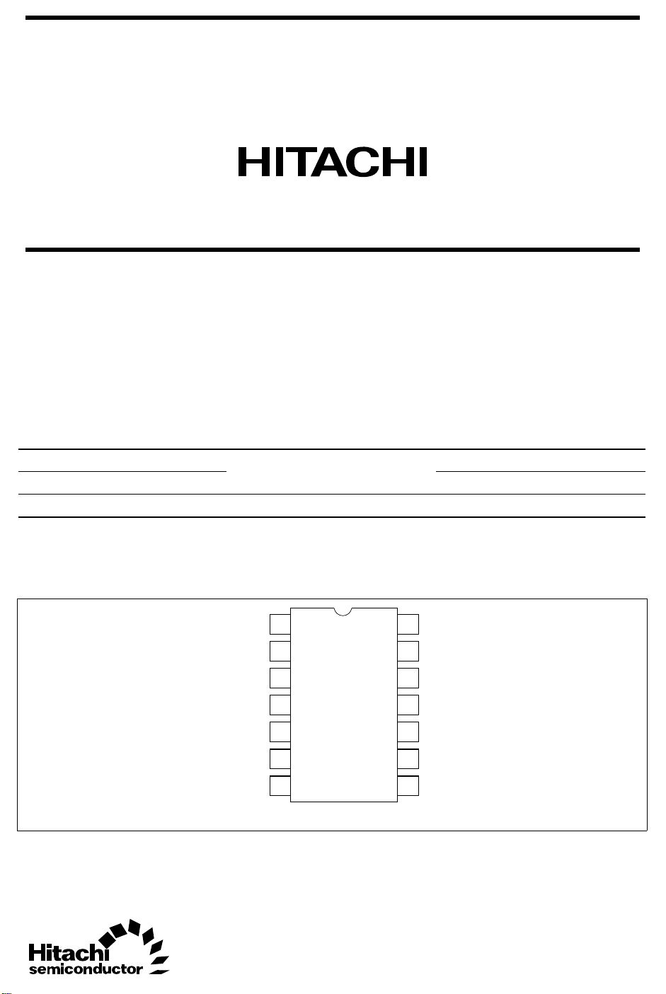
Pin Arrangement
NC
CURRENT
LIMIT
CURRENT
SENSE
(–)
V
IN
V
(+)
IN
V
REF
V
EE
1
2
3
4
5
6
7
(Top View)
14
13
12
11
10
NC
COMP
V
CC
V
C
V
OUT
V
9
8
Z
NC
HA17723/F/P
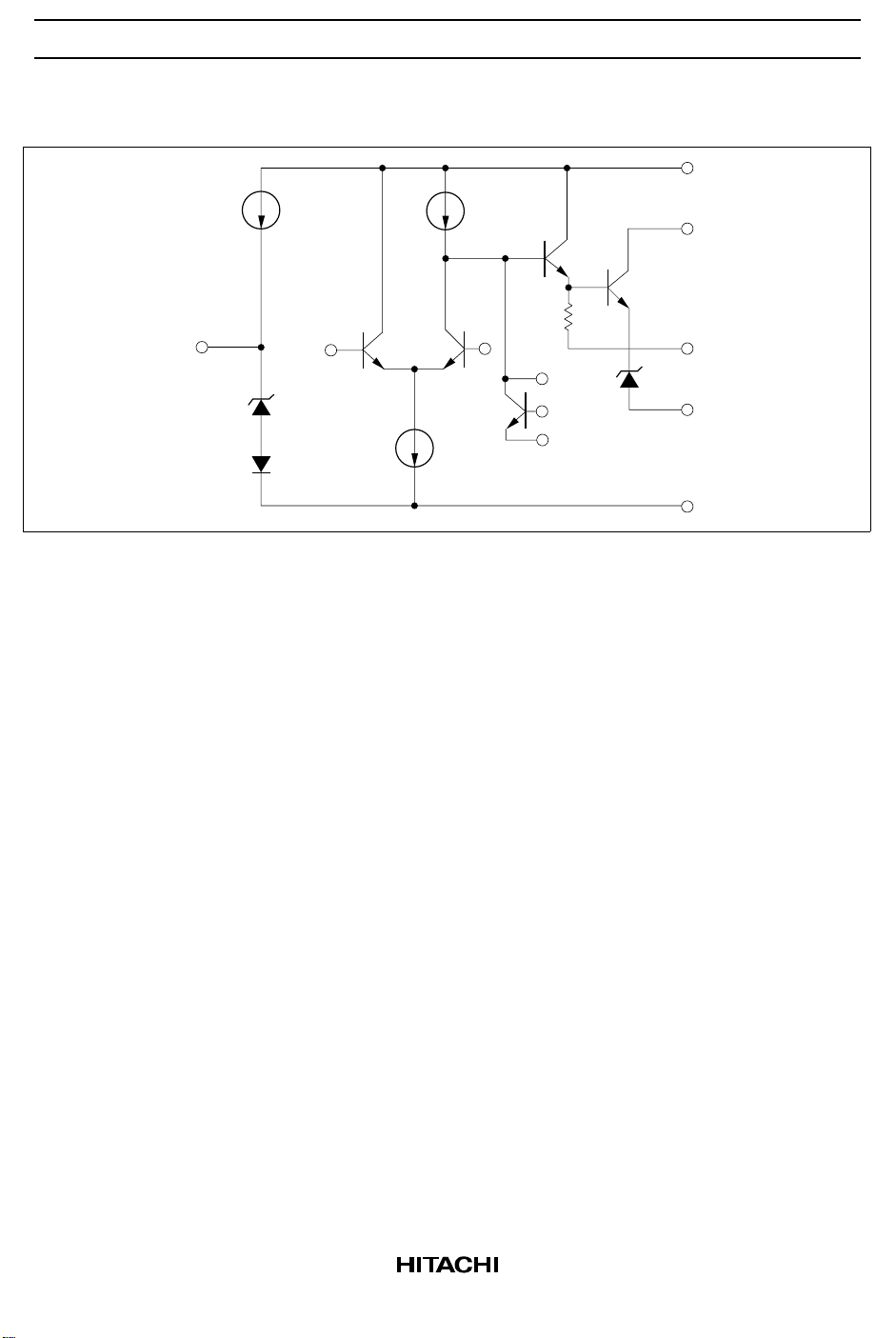
Circuit Schematic
V
REF
VIN (+)
V
CC
V
C
(–)
V
IN
V
OUT
COMP
CL
V
Z
CS
V
EE
2
HA17723/F/P
Absolute Maximum Ratings (Ta = 25°C)
Item Symbol HA17723/P HA17723F Unit
Supply voltage VCC 40 40 V
Input/Output voltage differential Vdiff (IN-O) 40 40 V
Differential input voltage VIN (diff) ±5 ±5V
Maximum output current I
Current from VREF I
Power dissipation P
OUT
REF
T
Operating temperature Topr 0 to +70 / –20 to +75 0 to +70 °C
Storage temperature Tstg –55 to +125 –55 to +125 °C
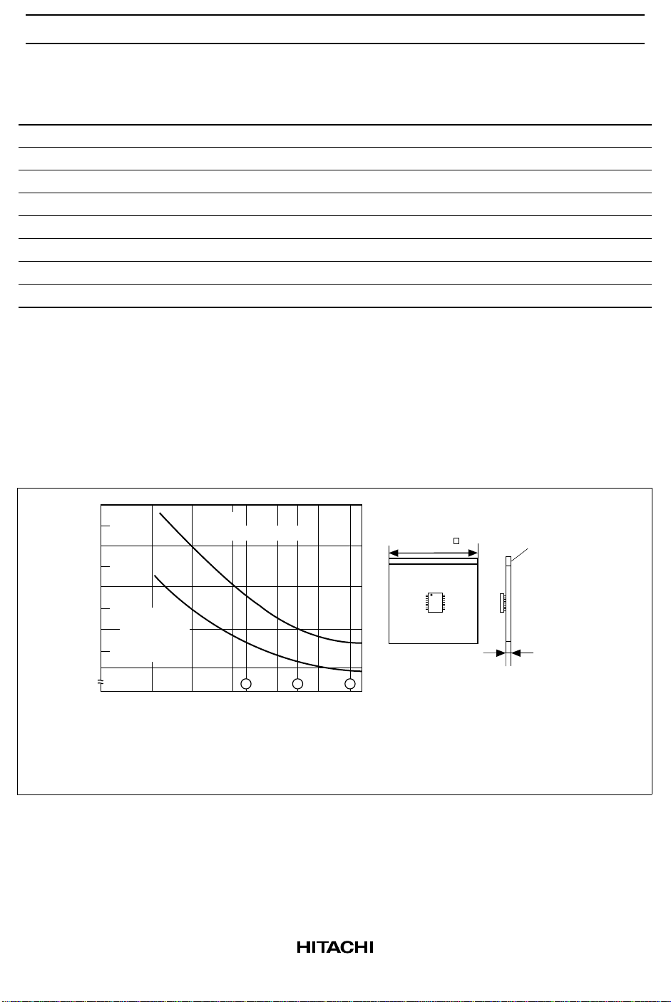
Notes: 1. Above 25°C derate by 8.3mW/°C
2. Allowable temperature of IC junction part, Tj (max), is as shown below.
Tj (max) = θj - a • Pc (max)+Ta
(θj - a is thermal resistance value during mounting, and Pc (max) is the maximum value of IC
power dissipation.)
Therefore, to keep Tj (max) ≤ 125°C, wiring density and board material must be selected
according to the board thermal conductivity ratio shown below.
Be careful that the value of Pc (max) does not exceed that P
150 150 mA
15 15 mA
830 (Note 1) 625 (Note 2) mW
.
T
240
220
SOP14
without compound
200
180
160
140
120
100
SOP14
using paste
containing
compound
80
Thermal resistance θj–a (°C/W)
21
0.5 1 2 5 10 20
Board thermal conductivity (W/m°C)
(1) Glass epoxy board with 10% wiring density
(2) Glass epoxy board with 30% wiring density
(3) Ceramic board with 96% alumina coefficient
40 mm
Board
0.8 t ceramic or
1.5 t epoxy
3
3
HA17723/F/P
Electrical Characteristics (Ta = 25°C)
Item Symbol Min Typ Max Unit Test Conditions
Line regulation δV
Load regulation δVO Load — 0.03 0.2 % I
Ripple rejection R
Average temperature
coefficient of output voltage
Reference voltage V
Standby current I
Short circuit current limit I
Line — 0.01 0.1 % VIN = 12 to 15V
O
— 0.1 0.5 % VIN = 12 to 40V
——0.4%V
= 12 to 15V,
IN
TA = –20 to +75°C
——0.3%V
= 12 to 15V,
IN
Ta = 0 to +70°C
= 1 to 50mA
OUT
——0.7%V
= 12 to 15V,
IN
TA = –20 to +75°C
——0.6%I
= 1 to 50mA,
OUT
Ta = 0 to +70°C
REJ
— 74 — dB f = 50Hz to
10kHz
—86— C
δVO/δT — 0.003 0.018 %/°C TA = –20 to +75°C
— 0.003 0.015 %/°C Ta = 0 to +70°C
REF
ST
SC
6.80 7.15 7.50 V VIN = VCC = VC = 12V,
V
= 0
EE
— — 4.0 mA VIN = 30V, IL = 0
— 65 — mA RSC = 10Ω, V
OUT
C
= 0
REF
REF
= 0
= 5µF
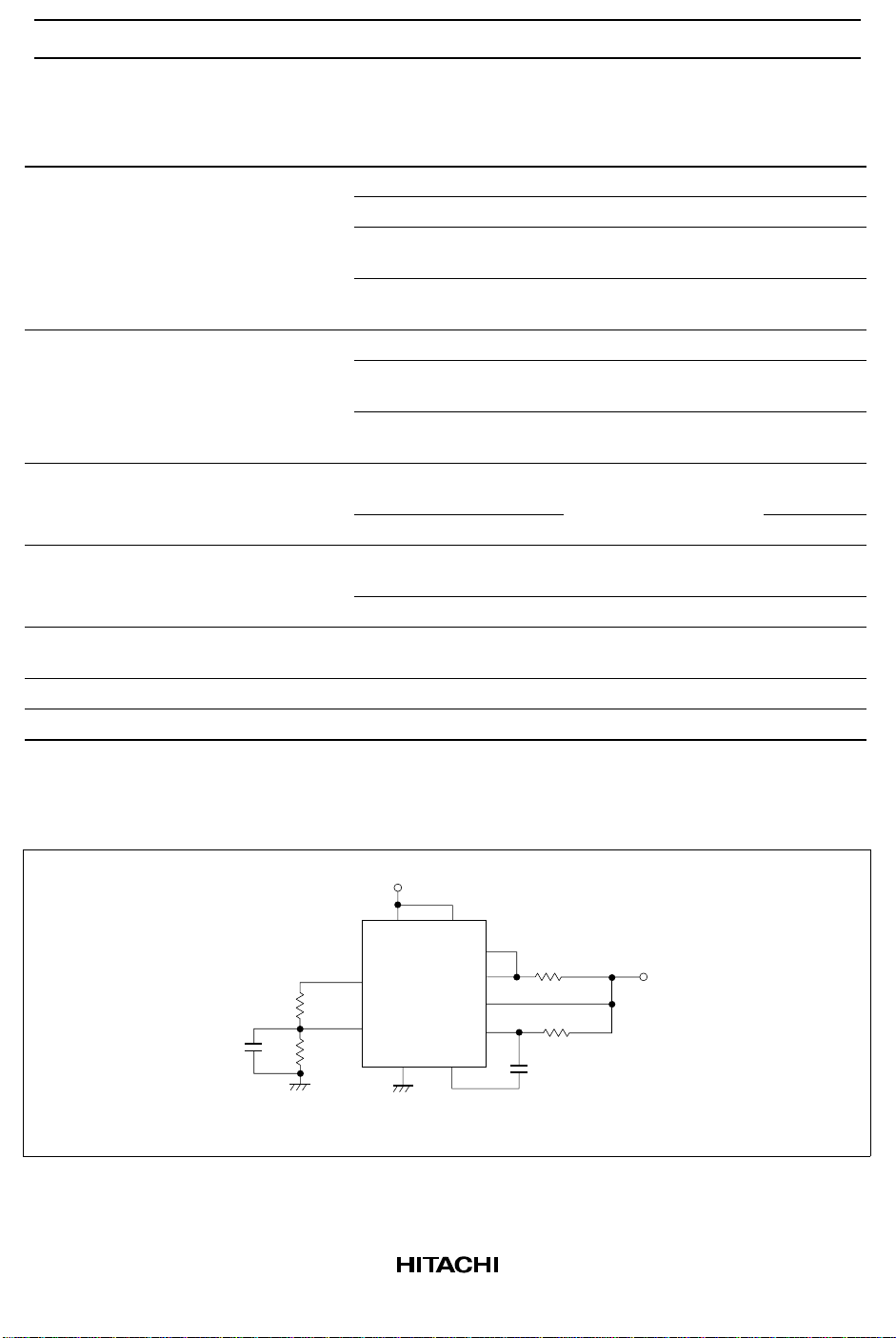
Electrical Characteristics Measuring Circuit
V
IN
C
REF
VIN = VCC = VC = 12V, VEE = 0, V
RSC = 0, C1 = 100pF, C
= 0, R2 ≈ 5kΩ, R3 = R1R2/(R1+R2)
REF
4
R
1
VIN(+)
R
2
= 5.0V, IL = 1mA,
OUT
V
V
REF
V
CC
C
V
V
EE
IN
COMP
V
OUT
CL
CS
(+)
R
SC
R
3
C
1
V
OUT
HA17723/F/P
HA17723 Applications
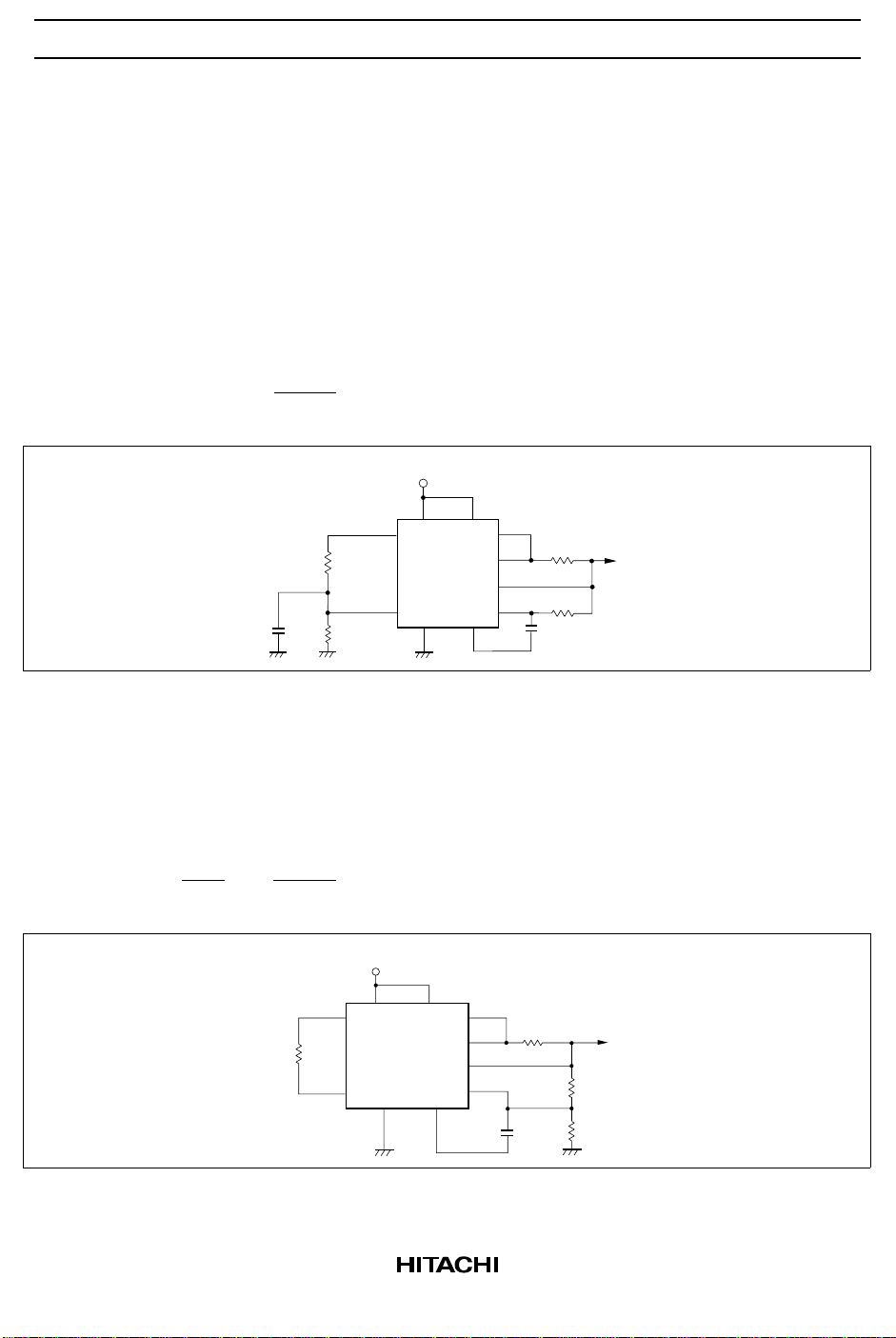
Fixed Voltage Source in Series
Low Voltage (2 to 7 V) Regulator: Figure 1 shows the construction of a basic low voltage regulator. The
divider (resistors R1 and R2) from V
noninverted input of the error amplifier, less than output voltage. In the fixed voltage source where the
output voltage will be fed back to the error amplifier directly as shown in figure 1. Output voltage will be
divided VREF since the output voltage is equal to the reference voltage.
makes the reference voltage, which will be provided to the
REF
Thus, the output voltage V
V
= nV
OUT
REF
OUT
, n =
C
REF
1µF
is:
R1 + R
R
2
2
R
1
2.15kΩ
R
2
4.99kΩ
V
IN
V
CC
V
REF
V
IN
(+)
V
EE
V
V
V
OUT
CL
CS
(–)
IN
COMP
C
R
= 0
R
3
SC
1.5kΩ
C
1
100pF
V
OUT
Figure 1 Low Voltage (2 to 7 V) Regulator
High Voltage (7 to 37 V) Regulator: Figure 2 shows the construction of a regulator whose output voltage
is higher than the reference voltage, V
REF
. V
is added to the non-inverted input of the error amplifier via
REF
a resistor, R3. The feedback voltage is produced by dividing the output voltage with resistors R1 and R2.
Thus, the output voltage V
V
V
OUT
REF
= , n =
n
OUT
is:
R1 + R
R
2
2
V
IN
V
V
IN
V
C
OUT
CL
CS
(–)
COMP
RSC = 0
C
1
100pF
R
3.8kΩ
V
CC
V
REF
3
V
(+)
IN
V
EE
Figure 2 High Voltage (7 to 37 V) Regulator
V
R
1
7.87kΩ
R
2
7.15kΩ
OUT
5
HA17723/F/P
Negative Voltage Regulator: Figure 3 shows the construction of a so-called negative voltage regulator,
which generates a negative output voltage with regard to GND. Assume that the output voltage, –V
increases in the negative direction. As the voltage across the R1 is larger than that across the R3, which
provides the reference voltage, the output current of the error amplifier increases. In the control circuit, the
impedance decreases with the increase of input current, which makes the base current of the external
transistor Q approach GND. As a result, the output voltage returns to the established value and output
voltage is stable.
The output voltage –VOUT of this circuit is:
OUT
,
–V
OUT
R1 + R
= –
R3 + R
= – V
R
· (R3 + R4) – R4 · (R1 + R2)
2
R
2
3
×
V
REF
R
4
1
(R1 + R2) · (R3 + R4)
V
R
2
R
3kΩ
11.5kΩ
4
V
CC
REF
×
R3 + R
V
OUT
V
V
CL
R
3
REF
4
V
C
R
5
2kΩ
Z
IN
Q
CS
VIN(+) VIN(–)
C
R
3kΩ
3
R
3.65kΩ
V
1
EE
COMP
1
100pF
V
OUT
Figure 3 Negative Voltage Regulator
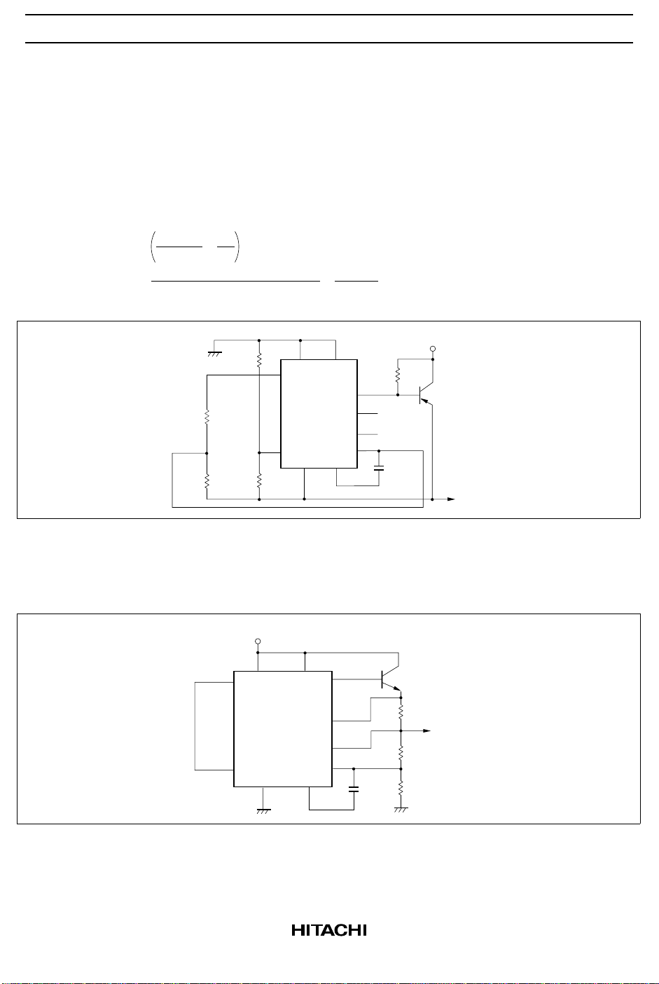
How to Increase the Output Current: To increase the output current, you must increase the current
capacity of the control circuit. Figures 4 and 5 show examples with external transistors.
V
IN
V
CC
V
REF
VIN(+) VIN(–)
V
EE
V
V
OUT
CL
CS
COMP
C
Q
R
SC
0.7Ω
V
OUT
R
1
7.87kΩ
C
500pF
R
1
2
7.15kΩ
Figure 4 Increasing Output Current (1)
6

V
IN
R
3
R
2.15kΩ
R
5.0kΩ
V
CC
V
REF
1
60Ω
V
C
V
OUT
CL
CS
V
(+) VIN(–)
2
IN
V
COMP
EE
C
1
1nF
Q
Figure 5 Increasing Output Current (2)
Fixed Voltage Source in Parallel Control
Figure 6 shows the circuit of a fixed voltage source in parallel control.
V
IN
R
4
100Ω
Q
1
R
2kΩ
R
5kΩ
V
CC
V
REF
1
V
V
OUT
V
C
R
Z
3
100Ω
CL
CS
(–)
V
2
V
EE
COMP
IN
C
1
5nF
R
SC
0.4Ω
V
OUT
V
HA17723/F/P
OUT
Figure 6 Fixed Voltage Source in Shunt Regulator
Switching Regulator
Figure 7 shows a switching regulator circuit. The error amplifier, control circuit, and forward feedback
circuit R4 and R3 operate in together as a comparator, and make the external transistors Q1 and Q2 to turn
on/off. In this circuit, the self-oscillation stabilizes the output voltage and the change in output is absorbed
by the changes of the switches conducting period.
Figures 8 and 9 show a negative voltage switching regulator circuit and its characteristics.
7

HA17723/F/P
V
IN
100Ω
R
5
V
V
C
EE
3kΩ
CL
CS
COMP
Q
R
51Ω
1
6
2.15kΩ
C
0.1µF
V
CC
V
REFVOUT
R
1
R
3
VIN(+)VIN(–)
1kΩ
R
1
R
2
5kΩ
4
1MΩ
Figure 7 Positive Voltage Switching Regulator
R
7
1kΩ
Z
C1 15pF
C
0.1µF
3.65kΩ
V
V
CC
R
2
4kΩ
1
1kΩ
R
3
R
R
4
1
1MΩ
V
C
V
REF
V
OUT
V
CL
CS
VIN(+) VIN(–)
COMP
EE
Q
D
100Ω
R
5
R
6
220Ω
Q
1
2
L
1
1
1.2mH
V
OUT
5V
C
2
100µF
V
IN
Q
2
D
1
L
1
1.2mH
V
OUT
–15V
C
2
100µF
Figure 8 Negative Voltage Switching Regulator
8

HA17723/F/P
–24
–20
(V)
–16
OUT
–12
–8
Output Voltage V
–4
–4 –8 –12 –16 –20 –24 –28 –32 –36 –40
–15.360
–15.340
(V)
–15.320
OUT
–15.300
Input – Output Characteristics
Ta = 25°C
Input Voltage V
(V)
IN
Line Regulation
I
= 0.2A
OUT
Ta = –25°C
25
–15.280
75
Output Voltage V
–15.260
–15.240
–24 –28 –32 –36 –40
Input Voltage V
(V)
IN
Load Regulation
–15.600
(V)
–15.500
OUT
–15.400
Ta = –25°C
VIN = 25 V
–15.300
25 75
–15.200
Output Voltage V
–15.100
0 0.2
0.6
0.4
Output Current I
0.8
1.0
1.2
OUT
1.4
(A)
1.6
1.8
2.0
Figure 9 Negative Voltage Switching Regulator Operating Characteristics
9

HA17723/F/P
Floating-Type Fixed Voltage Source
Voltage sources of the floating type or boost type are typically employed when high voltage output is
required. Figure 10 shows the circuit of a floating-type fixed voltage source. Considering the stabilization
in this circuit, assume that the output voltage increases. At the input terminal of the error amplifier the noninverted input will become low compared with the inverted input, and the output current of the error
amplifier decreases. Then, the current from the terminal VZ in the control circuit decreases. As a result the
base current of the external resistor Q1 will decrease and collector current will decrease, controlling
increase of the output voltage.
The output voltage V
V
= – 1 V
OUT
in the circuit in figure 10
OUT
R1 + R
R3 + R
R
2
4
×
R
4
1
REF
Figure 11 is the circuit diagram of a negative fixed voltage source in floating type.
V
IN
R5 6.2kΩ
V
C
OUT
V
Z
CL
CS
COMP
2.0W
C
1nF
Q
R
SC
1Ω
1
V
OUT
D 12 V
HZ12
R
53.7kΩ
V
CC
REF
V
V
R
4
3.0kΩ
H
R
1
3.57kΩ
VIN(+)
VIN(–)
2
R
3
3.0kΩ
V
EE
Figure 10 Positive Voltage Floating Regulator
10
R
5
R
97.6kΩ
R
3.57kΩ
V
10kΩ
D12 V
HZ12
2
CC
V
REF
H
R
3
3kΩ
VIN(+)
R
1
3kΩ
4
V
EE
V
V
IN
COMP
OUT
V
CL
CS
(–)
V
C
10kΩ
Z
C
100pF
Figure 11 Negative Voltage Floating Regulator
V
IN
R
6
Q
1
V
OUT

Fixed Voltage Source with Reduction Type Current Limiter
V
IN
R
2
2.15kΩ
R
1
5.0kΩ
V
CC
V
VIN(+)
V
EE
REF
COMP
V
V
C
OUT
R
CL
CS
(–)
V
IN
C
1
1nF
Figure 12 Fixed Voltage Source with Reduction Type Current Limiter
6.0
V
O
I
OP
(V)
OUT
5.0
4.0
3.0
30Ω
R
SC
3
V
OUT
2.7kΩ
R
4
5.6kΩ
R3 + R
R4 ⋅ R
4
SC
R
R4 ⋅ R
⋅ V
3
IOS =
IOP = IOS + ⋅ V
HA17723/F/P
BE
O
SC
2.0
Output Voltage V
1.0
0
I
OS
0
Output Current I
100
OUT
(mA)
200
Figure 13 Current Control Characteristics of Fixed Voltage Source
with Reduction Type Current Limiter
11

HA17723/F/P
Fixed Voltage Source Switching External Control
V
IN
V
CC
V
REF
R
1
2.15kΩ
VIN(+)
R
2
V
COMP
4.99kΩ
EE
Figure 14 Fixed Voltage Source Switching External Control
6
5
(V)
OUT
4
V
C
V
OUT
CL
CS
VIN(–)
C
1
1nF
Ta = 25°C
R
2kΩ
3
2SC458 K
R
T
5Ω
1
SC
Note
R
2kΩ
4
V
OUT
Note: Insert when
V
≥ 10V
OUT
Control Signal
3
2
1
Output Voltage V
0
0 4 8 1216202428323640
Time (sec)
Figure 15 Operating Characteristics of Fixed Voltage Source Switching External Control
12

Characteristic Curves
Load Regulation vs. Output Current-1 Load Regulation vs. Output Current-2
0.2
V
= +5V
OUT
V
= +12V
IN
R
= 0
(%)
SC
0.2
V
OUT
V
IN
R
(%)
= +5V
= –12V
= 10Ω
SC
HA17723/F/P
25
Ta = 75°C
–20
OUT
–20
25
V
OUT
V
= +12V
IN
R
= 10Ω
SC
= +5V
O Load
0.1
Ta = 75°C
Load Regulation δV
0102030
Output Current I
OUT
(mA)
5
4
(mA)
ST
3
Ta = –20°C
25
75
O Load
0.1
Load Regulation δV
0 20406080100
Output Current I
Relative Output Voltage vs. Output Current Stand-by Current vs. Input Voltage
1.2
1.0
0.8
0.6
Ta = 75°C
2
0.4
V
I
–20
OUT
OUT
25
= V
= 0
REF
Relative Output Voltage (V/V)
0.2
0 20406080100120
Output Current I
OUT
(mA)
Stand-by Current I
1
0 1020304050
Input Voltage VIN (V)
13

HA17723/F/P
Input/Output Voltage Differential-1
Line Regulation vs.
0.2
V
= +5V
OUT
R
= 0
SC
I
= 1mA
(%)
O Line
0.1
Line Regulation δV
0
–5 5 15253545
Input/Output Voltage Differential Vdiff(IN-O) (V)
Current Limiting Characteristics Line Transient Response
0.9
0.8
0.7
Sense Voltage
(V)
SC
0.6
0.5
0.4
Sense Voltage V
0.3
Limit Current
0.2
0.1
–100 0 100 200
Junction Temperature Tj(°C)
OUT
V = +3V
RSC = 5Ω
RSC = 10Ω
200
150
100
50
Input/Output Voltage Differential-2
0.2
(%)
O Line
0.1
Line Regulation δV
0
–5 5 15253545
Input/Output Voltage Differential Vdiff(IN-O) (V)
Input Voltage
(dev) (mV)
O
(mA)
SC
10
5
0
Limit Current I
Output Voltage
–5
–10
Output Voltage Differential V
Line Regulation vs.
V
OUT
R
SC
I
OUT
5µs/div
Time (µs)
= +5V
= 0
= 1mA to
50mA
VIN = +12V
V
= +5V
OUT
I
= 1mA
OUT
R
= 0
SC
6
4
2
(dev) (V)
IN
0
–2
–4
Input Voltage Differential V
14

HA17723/F/P
Load Transient Response Output Impedance vs. Frequency
Output Current
(dev) (mV)
O
Output Voltage
5
0
–5
–10
Output Voltage Differential V
5µs/div
Time (µs)
VIN = +12V
V
= +5V
OUT
I
= 40mA
OUT
R
= 0
SC
10
V
1.0
OUT
V
= +12V
IN
R
= 0
SC
I
= 50mA
L
10
5
0
(dev) (mA)
O
–5
0.1
Output Impedance Zout (Ω)
Output Current Differential I
100 1 k 10 k 100 k 1 M
= 5V
Frequency f (Hz)
CL = 0
CL = 1µF
15

HA17723/F/P
Package Dimensions
1
19.20
20.32 Max
1.30
Unit: mm
814
6.30
7.40 Max
7
2.54 ± 0.25
10.5 Max
14
1
1.27
2.39 Max
10.06
1.42 Max
0.48 ± 0.10
8
5.5
7
2.20 Max
2.54 Min 5.06 Max
0.51 Min
Hitachi Code
JEDEC
EIAJ
Mass
7.80
0.20 ± 0.04
*0.22 ± 0.05
0.70 ± 0.20
7.62
+ 0.10
0.25
– 0.05
0° – 15°
(reference value)
+ 0.20
– 0.30
1.15
0° – 8°
DP-14
Conforms
Conforms
0.97 g
Unit: mm
*0.42 ± 0.08
0.40 ± 0.06
*Dimension including the plating thickness
Base material dimension
16
0.12
0.10 ± 0.10
0.15
M
Hitachi Code
JEDEC
EIAJ
Mass
(reference value)
FP-14DA
—
Conforms
0.23 g

HA17723/F/P
Cautions
1. Hitachi neither warrants nor grants licenses of any rights of Hitachi’s or any third party’s patent,
copyright, trademark, or other intellectual property rights for information contained in this document.
Hitachi bears no responsibility for problems that may arise with third party’s rights, including
intellectual property rights, in connection with use of the information contained in this document.
2. Products and product specifications may be subject to change without notice. Confirm that you have
received the latest product standards or specifications before final design, purchase or use.
3. Hitachi makes every attempt to ensure that its products are of high quality and reliability. However,
contact Hitachi’s sales office before using the product in an application that demands especially high
quality and reliability or where its failure or malfunction may directly threaten human life or cause risk
of bodily injury, such as aerospace, aeronautics, nuclear power, combustion control, transportation,
traffic, safety equipment or medical equipment for life support.
4. Design your application so that the product is used within the ranges guaranteed by Hitachi particularly
for maximum rating, operating supply voltage range, heat radiation characteristics, installation
conditions and other characteristics. Hitachi bears no responsibility for failure or damage when used
beyond the guaranteed ranges. Even within the guaranteed ranges, consider normally foreseeable
failure rates or failure modes in semiconductor devices and employ systemic measures such as failsafes, so that the equipment incorporating Hitachi product does not cause bodily injury, fire or other
consequential damage due to operation of the Hitachi product.
5. This product is not designed to be radiation resistant.
6. No one is permitted to reproduce or duplicate, in any form, the whole or part of this document without
written approval from Hitachi.
7. Contact Hitachi’s sales office for any questions regarding this document or Hitachi semiconductor
products.
Hitachi, Ltd.
Semiconductor & Integrated Circuits.
Nippon Bldg., 2-6-2, Ohte-machi, Chiyoda-ku, Tokyo 100-0004, Japan
Tel: Tokyo (03) 3270-2111 Fax: (03) 3270-5109
URL NorthAmerica : http:semiconductor.hitachi.com/
For further information write to:
Hitachi Semiconductor
(America) Inc.
179 East Tasman Drive,
San Jose,CA 95134
Tel: <1> (408) 433-1990
Fax: <1>(408) 433-0223
Europe : http://www.hitachi-eu.com/hel/ecg
Asia (Singapore) : http://www.has.hitachi.com.sg/grp3/sicd/index.htm
Asia (Taiwan) : http://www.hitachi.com.tw/E/Product/SICD_Frame.htm
Asia (HongKong) : http://www.hitachi.com.hk/eng/bo/grp3/index.htm
Japan : http://www.hitachi.co.jp/Sicd/indx.htm
Hitachi Europe GmbH
Electronic components Group
Dornacher Straβe 3
D-85622 Feldkirchen, Munich
Germany
Tel: <49> (89) 9 9180-0
Fax: <49> (89) 9 29 30 00
Hitachi Europe Ltd.
Electronic Components Group.
Whitebrook Park
Lower Cookham Road
Maidenhead
Berkshire SL6 8YA, United Kingdom
Tel: <44> (1628) 585000
Fax: <44> (1628) 778322
Hitachi Asia Pte. Ltd.
16 Collyer Quay #20-00
Hitachi Tower
Singapore 049318
Tel: 535-2100
Fax: 535-1533
Hitachi Asia Ltd.
Taipei Branch Office
3F, Hung Kuo Building. No.167,
Tun-Hwa North Road, Taipei (105)
Tel: <886> (2) 2718-3666
Fax: <886> (2) 2718-8180
Copyright ' Hitachi, Ltd., 1998. All rights reserved. Printed in Japan.
Hitachi Asia (Hong Kong) Ltd.
Group III (Electronic Components)
7/F., North Tower, World Finance Centre,
Harbour City, Canton Road, Tsim Sha Tsui,
Kowloon, Hong Kong
Tel: <852> (2) 735 9218
Fax: <852> (2) 730 0281
Telex: 40815 HITEC HX
17
 Loading...