

Page 1
SERVICE MANUAL
Be sure to read this manual before servicing. To assure safety from fire, electric shock, injury, harmful radiation
and materials, various measures have been provided for in this HITACHI Plasma displayservice manual.
Be sure to read all cautionary items described in the manual to maintain safety before servicing.
Contents
1. Sincethe Panel Module and front Filter are made of glass, handlea broken Module and/or Filter with
sufficient care, in order not to be injured.
2. Repair work should not be started until after the Panel Module and the AC/DC Power supply have cooled
sufficiently.
3. Special care should be exercised in the proximity of the display area in order not to damage its surface.
4. The Panel Module should not be touched with bare hands, as this will protect its surface from stains.
5. It is recommended to use clean soft gloves during the repair work in order to protect not only the display
area of the Panel Module but also the technician.
6. The Chip Tube of the Panel Module (located in the upper left corner of the back of the glass panel)
is very fragile; as well, the flat cables connecting the Panel to the drive circuit PWBs are very weak. Take
care not to damage these, otherwise, the panel will never light again.
Service Warning
Caution
1. Safety Precaution------------------------------------2
2. Precaution --------------------------------------------21
3. Features ----------------------------------------------21
4. Specifications----------------------------------------22
5. Service Points---------------------------------------27
6. Service Mod e A c c e s s --------------------------------28
7. Troubleshooting Flow Chart----------------------55
8. Block Diagram---------------------------------------58
9. Connector Connection Diagram-----------------61
10. Circuit Board Layers-----------------------------63
11. Basic Circuit Diagram----------------------------64
12. Printed Wiring Board Diagram-----------------68
13. Disassembly Diagram----------------------------71
14. Replacement Parts List ---------------------------- 72
15. DC Voltages -----------------------------------------74
16. Speaker Installation ------------------------------- 82
CH 1, CH 2
Version 0198.3
NN TT SS CC
PA
42EDT41A
CMP420V1A / CMP420V2A
PPWW11AA
R/C: CLU-W900 / SMK
CChhaassssiiss
TO GO TO A CHAPTER, CLICK ON ITS HEADING BELOW
No. 0198
SPECIFICATIONS AND PARTS ARE SUBJECT TO CHANGE FOR IMPROVEMENT
NOVEMBER 2004 HHEA-MANUFACTURING DIVISION
PLASMA DISPLAY PANEL
CH 3
Page 2
SAFETY PRECAUTIONS
LEAKAGE
CURRENT
TESTER
(READING
SHOULD NOT
BE ABOVE 0.5MIU)
EARTH
GROUND
TEST ALL
EXPOSED
METAL SURFACES
DEVICE
UNDER
TEST
3-WIRE CORD
ALSO TEST WITH PLUG
REVERSED
(USING AC ADAPTER
PLUS AS REQUIRED)
NOTICE: Comply with all cautions and safety-related notes
located on or inside the cover case and on the chassis or plasma
module.
WARNING: Since the chassis of the AVC unit and Plasma Panel
unit is connected to both sides of the AC power supply during
operation, whenever the receiver is plugged in, service should
not be attempted by anyone unfamiliar with the precautions
necessary when working on this type of receiver.
1. When service is required, an isolation transformer should be
inserted between power line and the receiver before any
service is performed on a “HOT” chassis receiver.
2. When replacing a chassis in the receiver, all the protective
devices must be put back in place, such as barriers, nonmetallic knobs, insulating cover-shields, and isolation
resistors, capacitors, etc.
3. When service is required, observe the original lead dress.
4. Always use manufacturer’s replacement components. Critical
components as indicated on the circuit diagram should not be
replaced by another manufacturer’s. Furthermore, where a
short circuit has occurred, replace those components that
indicate evidence of over heating.
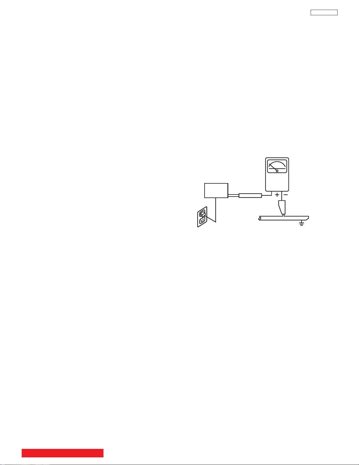
PW1A
Leakage Current Hot Check
This check must be done considering the AVC or the PDP
monitor as one instrument each.
With any of the instruments completely reassembled (being
the instrument either the AVC center or the PDP monitor), plug
the AC line cord directly into a 120V AC outlet. (Do not use an
isolation transformer during this test.) Use a leakage current
tester or a metering system that complies with the American
National Standards Institute (ANSI) C101.0 Leakage Current
for Appliances. In the case of the PDP monitor set the AC
switch first in the ON position and then in the OFF position,
measure from across Line 1 and Line 2 of the three plug
prongs, do not connect with the third prong, which is physical
ground, to all exposed metal parts of the instrument
(antennas, handle bracket, metal cabinet, screw heads,
metallic overlays, control shafts, etc.), especially any exposed
metal parts that offer an electrical return path to the chassis.
Any current measured must not exceed 0.5 MIU. Reverse the
instrument power cord plug in the outlet and repeat test.
AC LEAKAGE TEST
5. Before returning a serviced receiver to the customer, the
service technician must thoroughly test the unit to be certain
that it is completely safe to operate without danger of electrical
shock, and be sure that no protective device built into the
receiver by the manufacturer has become defective, or
inadvertently defeated during servicing.
Therefore, the following checks should be performed for the
continued protection of the customer and service technician.
Leakage Current Cold Check
With the AC plug removed from the 120V AC 60Hz source,
place a jumper across Line 1 and Line 2 of the three plug
prongs, do not connect with the third prong, which is physical
ground.
Using an insulation tester (DC500V), connect one of its leads
to the AC plug jumper and touch with the other lead each
exposed metal part (antennas, screwheads, metal overlays,
control shafts, etc.), particularly any exposed metal part
having a return path to the chassis should have a resistor
reading over 4MΩ. Any resistance value below this range
indicates an abnormality which requires corrective action. An
exposed metal part not having a return path to the chassis will
indicate an open circuit.
ANY MEASUREMENTS NOT WITHIN THE LIMITS OUTLINED
ABOVE ARE INDICATIVE OF A POTENTIAL SHOCK HAZARD
AND MUST BE CORRECTED BEFORE RETURNING THE
RECEIVER TO THE CUSTOMER.
TABLE OF CONTENTS
2
Page 3

PRODUCT SAFETY NOTICE
Many electrical and mechanical parts in HITACHI television
receivers have special safety-related characteristics. These are
often not evident from visual inspection nor can the protection
afforded by them necessarily be obtained by using replacement
components rated for higher voltage, wattage, etc. Replacement
parts which have these special safety characteristics are
identified in this Service Manual.
Electrical components having such features are identified with a
!
1 mark in the schematics and parts list in this Service Manual.
The use of a substitute replacement component which does not
have the same safety characteristics as the HITACHIrecommended replacement component, shown in the parts list in
this Service Manual, may create shock, fire, X-radiation, or other
hazards.
Product safety is continuously under review and new instructions
are issued from time to time. For the latest information, always
consult the current HITACHI Service Manual. A subscription to,
or additional copies of HITACHI Service Manuals may be
obtained at a nominal charge from HITACHI Sales Corporation.
1. Follow the general caution recommendations from “Safety
precautions” section.
42EDT41A - Plasma Monitor Panel
CMP420V1A - Plasma Monitor Panel
CMP420V2A - Plasma Monitor Panel
1. Follow the general caution recommendations from “Safety
precautions” section.
2. Since the Panel module and front filter are made of glass,
sufficient care shall be taken when handling the broken
module and filter in order to avoid injury.
3. If necessary to replace Panel module, this work must be
started after the panel module and the AC/DC Power supply
becomes sufficiently cool.
4. Special care must be taken with the display area to avoid
damaging its surface.
5. The Panel Module shall not be touched with bare hands to
protect its surface from stains.
6. It is recommended to use clean soft gloves during the
replacing work of the Panel module in order to protect, not
only the display area of the panel module but also the
serviceman.
7. The Chip Tube of the panel module (located upper left of the
back of the panel module) and flexible cables connecting
Panel glasses to the drive circuitry Printed Wiring Boards
(P.W.B.) are very weak, so sufficient care must be taken to
prevent breaking or cutting any of these. If the Chip Tube
breaks the panel module will never work, replacement for a
new plasma panel module will be needed.
8. Signal, power supply P.W.B.’s and PDP driving circuits
P.W.B.’s are assembled on the rear side of the PDP module,
take special care with this fragile circuitry; particularly, Flexible
Printed Circuits bonded to surrounding edges of the glass
panel. They are not strong enough to withstand harsh outer
mechanical forces. Avoid touching the flexible printed circuits
by not only your hands, but also tools, chassis, or any other
object. Extreme bending of the connectors must be avoided
too. In case the flexible printed circuits are damaged, the
corresponding addressed portions of the screen will not be lit
and exchange of a glass panel will be required.
PW1A
PDP Module Handling
When there is need to replace a broken PDP module which is the
displaying device from the Plasma monitor unit, consider the
following:
1. When carrying the PDP module, two persons should stand at
both shorter-edge sides of the glass-panel and transport it with
their palms. Avoid touching the Flexible Printed Circuits or the
chip tube on the corner of the glass-panel. Handle only by the
surface of the glass panel. In case of some PDP modules,
electrode repair is done by connecting between regular
terminal with Cu tape and Cu wire. Please do not hook and/or
damage this repair line. If it is damaged, the module will not
function unless the glass-panel is exchanged with a new
glass-panel.
2. When carrying PDP module, watch surrounding objects, such
as tables, and also do not carry it alone since it may be
dangerous and it will be damaged due to excessive stress to
the module (glass-panel).
3. Please do not stand the module with the edge of the glasspanel on the table since this might result in damage to the
glass-panel and/or flexible printed circuits due to excessive
stress to the module (glass-panel).
WARNING
Lead in solder used in this product is listed by the California
Health and Welfare agency as a known reproductive toxicant
which may cause birth defects or other reproductive harm
(California Health and Safety Code, Section 25249.5).
When servicing or handling circuit boards and other components
which contain lead in solder, avoid unprotected skin contact with
solder. Also, when soldering make sure you are in a well
ventilated area in order to avoid inhalation of any smoke or
fumes released.
SAFETY NOTICE
USE ISOLATION TRANSFORMER
WHEN SERVICING
POWER SOURCE
This plasma television and the AVC Center is designed to
operate on 120 Volts/60Hz, AC house current. Insert the power
cord into a 120 Volts/60Hz outlet.
NEVER CONNECT THE PLASMA AND THE AVC CENTER TO
OTHER THAN THE SPECIFIED VOLTAGE OR TO DIRECT
CURRENT AND TO 50HZ. TO PREVENT ELECTRIC SHOCK,
DO NOT USE THE PLASMA TELEVISION’S (POLARIZED)
PLUG WITH AN EXTENSION CORD, RECEPTACLE, OR THE
OUTLETS UNLESS THE BLADES AND GROUND TERMINAL
CAN BE FULLY UNSERTED TO PREVENT BLADE
EXPOSURE.
TABLE OF CONTENTS
3
Page 4

SERVICING PRECAUTIONS
CAUTION: Before servicing instruments covered by this service
data and its supplements and addenda, read and follow the
“Important Safety Instructions” on page 3 of this publication.
NOTE: If unforeseen circumstances create conflict between the
following servicing precautions and any of the safety precautions
on page 3 of this publication, always follow the safety
precautions. Remember: Safety First.
General Servicing Guidelines
1. Always unplug the instrument AC power cord from the AC
power source before:
a. Removing or reinstalling any component, circuit board,
module, or any other instrument assembly.
b. Disconnecting or reconnecting any instrument electrical
plug or other electrical connection.
PW1A
Electrostatically Sensitive (ES) Devices
Some semiconductor (solid state) devices can be damaged
easily by static electricity. Such components commonly are called
Electrostatically Sensitive (ES) Devices. Examples of typical ES
devices are integrated circuits and some field-effect transistors
and semiconductor “chip” components. The following techniques
should be used to help reduce the incidence of component
damage caused by static electricity.
1. Immediately before handling any semiconductor component
or semiconductor-equipped assembly, drain off any
electrostatic charge on your body by touching a known earth
ground. Alternatively, obtain and wear a commercially
available discharging wrist strap device, which should be
removed for potential shock reasons prior to applying power to
the unit under test.
c. Connecting a test substitute in parallel with an electrolytic
capacitor in the instrument.
CAUTION: A wrong part substitution or incorrect polarity
installation of electrolytic capacitors may
result in an explosion hazard.
2. Do not spray chemicals on or near this instrument or any of its
assemblies.
3. Unless specified otherwise in these service data, clean
electrical contacts by applying the following mixture to the
contacts with a pipe cleaner, cotton-tipped stick or
comparable nonabrasive applicator: 10% (by volume)
Acetone and 90% (by volume) isopropyl alcohol (90%-99%
strength).
CAUTION: This is a flammable mixture. Unless specified
otherwise in these service data, lubrication of
contacts is not required.
4. Do not defeat any plug/socket of voltage interlocks with which
instruments covered by this service data might be equipped.
5. Do not apply AC power to this instrument and/or any of its
electrical assemblies unless all solid-state device heat-sinks
are correctly installed.
6. Always connect the test instrument ground lead to the
appropriate instrument chassis ground before connecting the
test instrument positive lead. Always remove the test
instrument ground lead last.
7. Use with this instrument only the test fixtures specified in this
service data.
CAUTION: Do not connect the test fixture ground strap to
any heatsink in this instrument.
2. After removing an electrical assembly equipped with ES
devices, place the assembly on a conductive surface such as
aluminum foil, to prevent electrostatic charge buildup or
exposure of the assembly.
3. Use only a grounded-tip soldering iron to solder or desolder
ES devices.
4. Use only an anti-static type solder removal device. Some
solder removal devices not classified as “anti-static” can
generate electrical charges sufficient to damage ES device.
5. Do not use freon-propelled chemicals. These can generate
electrical charges sufficient to damage ES devices.
6. Do not remove a replacement ES device from its protective
package until immediately before you are ready to install it.
(Most replacement ES devices are packaged with leads
electrically shorted together by conductive foam, aluminum foil
or comparable conductive material.)
7. Immediately before removing the protective material from the
leads of a replacement ES device, touch the protective
material to the chassis or circuit assembly into which the
device will be installed.
CAUTION: Be sure no power is applied to the chassis or
circuit, and observe all other safety precautions.
8. Minimize bodily motions when handling unpackaged
replacement ES devices. (Otherwise harmless motion such as
the brushing together of your clothes fabric or the lifting of your
foot from a carpeted floor can generate static electricity
sufficient to damage an ES device.)
TABLE OF CONTENTS
4
Page 5

PW1A
Use Soldering Iron to Pry Leads
General Soldering Guidelines
1. Use a grounded-tip, low-wattage soldering iron and
appropriate tip size and shape that will maintain tip
temperature within the range 500°F to 600°F.
2. Use an appropriate gauge of resin-core solder composed of
60 parts tin/40 parts lead.
3. Keep the soldering iron tip clean and well-tinned.
4. Thoroughly clean the surfaces to be soldered. Use a small
wire-bristle (0.5 inch or 1.25 cm) brush with a metal handle.
Do not use freon-propelled spray-on cleaners.
5. Use the following desoldering technique.
a. Allow the soldering iron tip to reach normal temperature
(500°F to 600°F).
b. Heat the component lead until the solder melts. Quickly
draw away the melted solder with an anti-static, suctiontype solder removal device or with solder braid.
CAUTION: Work quickly to avoid overheating the circuit
board printed foil.
6. Use the following soldering technique.
a. Allow the soldering iron tip to reach normal temperature
(500°F to 600°F).
b. First, hold the soldering iron tip and solder strand against
the component lead until the solder melts.
c. Quickly move the soldering iron tip to the junction of the
component lead and the printed circuit foil, and hold it
there only until the solder flows onto and around both the
component lead and the foil.
CAUTION: Work quickly to avoid overheating the circuit
board printed foil or components.
d. Closely inspect the solder area and remove any excess or
splashed solder with a small wire-bristle brush.
Removal
1. Desolder and straighten each IC lead in one operation by
gently prying up on the lead with the soldering iron tip as the
solder melts.
2. Draw away the melted solder with an anti-static suction-type
solder removal device (or with solder braid) before removing
the IC.
Replacement
1. Carefully insert the replacement IC in the circuit board.
2. Carefully bend each IC lead against the circuit foil pad and
solder it.
3. Clean the soldered areas with a small wire-bristle brush. (It is
not necessary to reapply acrylic coating to areas.)
“Small-signal” Discrete Transistor Removal/Replacement
1. Remove the defective transistor by clipping its leads as close
as possible to the component body.
2. Bend into a “U” shape the end of each of the three leads
remaining on the circuit board.
3. Bend into a “U” shape the replacement transistor leads.
4. Connect the replacement transistor leads to the
corresponding leads extending from the circuit board and
crimp the “U” with long nose pliers to insure metal to metal
contact, then solder each connection.
Power Output Transistor Devices Removal/Replacements
1. Heat and remove all solder from around the transistor leads.
2. Remove the heatsink mounting screw (if so equipped).
3. Carefully remove the transistor from the circuit board.
4. Insert new transistor in circuit board.
IC Removal/Replacement
Some Hitachi unitized chassis circuit boards have slotted holes
(oblong) through which the IC leads are inserted and then bent
flat against the circuit foil. When holes are the slotted type, the
following technique should be used to remove and replace the
IC. When working with boards using the familiar round hole, use
the standard technique as outlined in paragraphs 5 and 6 above.
TABLE OF CONTENTS
5. Solder each transistor lead, and clip off excess lead.
6. Replace heatsink.
Diode Removal/Replacement
1. Remove defective diode by clipping its leads as close as
possible to diode body.
2. Bend the two remaining leads perpendicularly to the circuit
board.
3. Observing diode polarity, wrap each lead of the new diode
around the corresponding lead on the circuit board.
4. Securely crimp each connection and solder it.
5. Inspect (on the circuit board copper side) the solder joints of
the two “original leads”. If they are not shiny, reheat them and,
if necessary, apply additional solder.
5
Page 6
PW1A
CRIMP AND
SOLDER
BARE JUMPER
WIRE
Install Jumper Wire and Solder
DEFECTIVE
COPPER
REMOVED
Insulated Jumper Wire
Fuses and Conventional Resistor Removal/Replacement
1. Clip each fuse or resistor lead at top of circuit board
hollow stake.
2. Securely crimp leads of replacement component around stake
1/8 inch from top.
3. Solder the connections.
CAUTION: Maintain original spacing between the replaced
component and adjacent components and the
circuit board, to prevent excessive component
temperatures.
Circuit Board Foil Repair
Excessive heat applied to the copper foil of any printed circuit
board will weaken the adhesive that bonds the foil to the circuit
board, causing the foil to separate from, or “lift-off,” the board.
The following guidelines and procedures should be followed
whenever this condition is encountered.
In Critical Copper Pattern Areas
High component/copper pattern density and/or special
voltage/current characteristics make the spacing and integrity of
copper pattern in some circuit board areas more critical than in
others. The circuit foil in these areas is designated as Critical
Copper Pattern. Because Critical Copper Pattern requires
special soldering techniques to ensure the maintenance of
reliability and safety standards, contact your Hitachi personnel.
At IC Connections
To repair defective copper pattern at IC connections, use the
following procedure to install a jumper wire on the copper pattern
side of the circuit board. (Use this technique only on IC
connections.)
1. Carefully remove the damaged copper pattern with a sharp
knife. (Remove only as much copper as absolutely
necessary.)
2. Carefully scratch away the solder resist and acrylic coating (if
used) from the end of the remaining copper pattern.
At Other Connections
Use the following technique to repair defective copper pattern at
connections other than IC Pins. This technique involves the
installation of a jumper wire on the component side of the circuit
board.
1. Remove the defective copper pattern with a sharp knife.
Remove at least 1/4 inch of copper, to ensure hazardous
condition will not exist if the jumper wire opens.
2. Trace along the copper pattern from both wire sides of the
pattern break and locate the nearest component directly
connected to the affected copper pattern.
3. Connect insulated 20-gauge jumper wire from the nearest
component on one side of the pattern break to the lead of the
nearest component on the other side.
Carefully crimp and solder the connections.
CAUTION: Be sure the insulated jumper wire is dressed so
that it does not touch components or sharp
edges.
3. Bend a small “U” in one end of a small-gauge jumper wire and
carefully crimp it around the IC pin. Solder the IC connection.
4. Route the jumper wire along the path of the cut-away copper
pattern and let it overlap the previously scraped end of the
good copper pattern. Solder the overlapped area, and clip off
any excess jumper wire.
TABLE OF CONTENTS
6
Page 7
PW1A
NOTE: These components are affixed with glue. Be careful not to break or damage any foil under the
component or at the pins of the ICs when removing. Usually applying heat to the component for a short time
while twisting with tweezers will break the component loose.
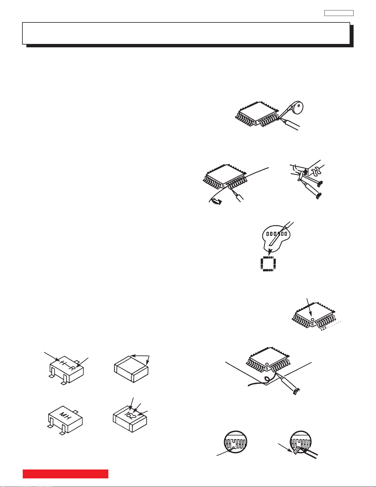
Leadless Chip Components
(surface mount)
Chip components must be replaced with identical chips
due to critical foil track spacing. There are no holes in the
board to mount standard transistors or diodes. Some chip
capacitor or resistor board solder pads may have holes
through the board, however the hole diameter limits
standard resistor replacement to 1/8 watt. Standard
capacitors may also be limited for the same reason. It is
recommended that identical chip components be used. .
Chip resistors have a three digit numerical resistance code
-1st and 2nd significant digits and a multiplier. Example:
162 = 1600 or 1.6KΩ resistor, 0 = 0Ω (jumper).
Chip capacitors generally do not have the value indicated
on the capacitor. The color of the component indicates the
general range of the capacitance.
Chip transistors are identified by a two letter code. The first
letter indicates the type and the second letter, the grade of
transistor.
Chip diodes have a two letter identification code as per the
code chart and are a dual diode pack with either
common anode or common cathode. Check the parts list
for correct diode number.
Component Removal
1. Use solder wick to remove solder from component end
caps or terminals.
2. Without pulling up, carefully twist the component with
tweezers to break the adhesive.
3. Do not reuse removed leadless or chip components
since they are subject to stress fracture during
removal .
Chip Component Installation
1. Put a small amount of solder on the board soldering
pads.
2. Hold the chip component against the soldering pads
with tweezers or with a miniature alligator clip and
apply heat to the pad area with a 30 watt iron until
solder flows. Do not apply heat for more than 3
seconds
How to Replace Flat-lC
—Required Tools—
• Soldering iron • iron wire or small awl
• De-solder braids • Magnifier
1. Remove the solder from all of the pins of a Flat-lC by
using a de-solder braid.
Flat-IC
2. Put the iron wire under the pins of the Flat-lC and pull
it in the direction indicated while heating the pins using
a soldering iron. A small awl can be used instead of
the iron wire.
Iron
Wire
Pull
Soldering
Iron
Soldering
3. Remove the solder from all of the pads of the FiatlC by using
a de-solder braid.
De-Solder
Braid
Flat-IC
4. Position the new Flat-lC in place (apply the pins of the
Flat-lC to the soldering pads where the pins need to be
soldered). Properly determine
the positions of the soldering
pads and pins by correctly
aligning the polarity symbol.
De-Solder
Braid
Soldering
Iron
Awl
Iron
Soldering
Iron
Polarity Symbol
TYPE
B
E
ANODES
MH DIODE
C
GRADE
TRANSISTOR
COMMON CATHODE
TABLE OF CONTENTS
Chip Components
SOLDER CAPS
1ST DIGIT
RESISTOR
SOLDER
CAPS
CAPACITOR
2ND DIGIT
MULTIPLIER
= 1600 = 1.6K
5. Solder all pins to the soldering pads using a fine tipped
soldering iron.
Solder
Soldering
Iron
6. Check with a magnifier for solder bridge between the
pins or for dry joint between pins and soldering pads. To
remove a solder bridge, use a de-solder braid as shown in
the figure below.
De-Solder
Braid
Bridge
Solder
7
Soldering
Iron
Page 8

AGENCY REGULATORY
INFORMATION
Federal Communications Commission Notice
This equipment has been tested and found to comply with the limits for a Class B digital device, pursuant to Part 15 of
the FCC Rules. These limits are designed to provide reasonable protection against harmful interference in a residential
installation. This equipment generates, uses and can radiate radio frequency energy and if not installed and used in
accordance with the instructions, may cause harmful interference to radio communications. However, there is no
guarantee that interference will not occur in a particular installation. If this equipment does cause harmful interference
to radio or television reception, which can be determined by turning the equipment off and on, the user is encouraged
to try to correct the interference by one or more of the following measures:
• Reorient or relocate the receiving antenna.
• Increase the separation between the equipment and the receiver.
• Connect the equipment into an outlet on a circuit different from that to which the receiver is connected.
• Consult the dealer or an experienced radio/television technician for help.
Modifications
The FCC requires the user to be notified that any changes or modifications made to this device that are not expressly
approved by Hitachi Home Electronics (America), Inc. may void the user’s warranty.
PW1A
Cables
Connections to this device must be made with shielded cables with metallic RFI/EMI connector hoods to maintain
compliance with FCC Rules and Regulations.
Any cables that are supplied with the system must be replaced with identical cables in order to assure compliance with
FCC rules. Order Hitachi spares as replacement cables.
Declaration of Conformity
This device complies with Part 15 of the FCC Rules. Operation is subject to the following two conditions: (1) this device
may not cause harmful interference and (2) this device must accept any interference received, including interference
that may cause undesired operation.
For questions regarding this declaration, contact:
Hitachi America, LTD.
Home Electronics Division
900 Hitachi Way
Chula Vista, CA 91914
Tel. 1-800-448-2244 (1-800-HITACHI)
ATTN: CUSTOMER RELATIONS
TABLE OF CONTENTS
8
Page 9
ACKNOWLEDGMENTS
AND TRADEMARKS
This Plasma Television complies with VESADDC2B specifications, Plug & Play
is a system with computer, peripherals (including monitors) and operating
system. It works when the monitor is connected to a DDC ready computer that
is running an operating system software that is capable for the plug & play.
When a Plug and Play PC is powered on, it sends a command to the Monitor
requesting identification. The Monitor sends back a string of data including its
characteristics.
TRADEMARK ACKNOWLEDGMENT
TM
DDC is a trademark of Video Electronics Standard Association.
IBM PC/AT and VGA are registered trademarkds of International Business Machines Corporation of the U.S.A.
Apple and Macintosh are registered trademarks of Apple Computer, Inc.
VESA is a trademark of a nonprofit organization, Video Electronics Standard Association.
PW1A
This Class B digital apparatus meets all requirements of the Canadian Interference-Causing Equipment Regulations.
This Class B digital apparatus complies with Canadian ICES-003.
Cet appareil numérique de la classe B est conforme à la norme NMB-003 du Canada.
Cable Compatible Television Apparatus- Tèlèvision câblocompatible, Canada.
Notes on Closed Caption:
This Plasma Television receiver will display television closed captioning, ( or ), in accordance with
paragraph 15.119 of the FCC rules.
TruBass and the SRS ®symbol are trademarks of SRS Labs, Inc. TruBass technology is incorporated under license
from SRS Labs, Inc.
TABLE OF CONTENTS
9
Page 10
Plasma TV
Hitachi RS232C Communication Specification
This document defines the detailed RS232C control protocol for the following Hitachi Plasma
Televisions:
Model: 42EDT41A
CMP420V1A
CMP420V2A
The Information enclosed is subject to change without notice. Please refer to revision number
shown above when inquiring about product support.
1. Hardware Interface
1.1- The cable interface to the monitor is a 9 pin D-Sub type.
1.2- The gender of the 9 pin D-sub on the monitor is male. Therefore, the cable interface to
the monitor should be female.
1.3- The cable is configured in a null modem wiring scheme
1.4- A pin reference illustrations is provided below:
Figure. 1 (a) Male 9 pin D-sub
(Outside View)
Figure. 1 (b) Female 9 pin D-Sub
(Outside View)
1.5- Electric: Electrical specification is based on the current RS232C standard.
2. Communication Format
2.1- Port Configuration
(1) Communications System: Asynchronous
(2) Bit Rate: 9600 bps
(3)Data Length: 7 bit
(4) Parity: None
(5) Start Bit: None
(6) Stop Bit: 1 bit
¬ ® ¯ °
±²³´
°¯®¬
´³²±
Pin #
Signal
Remark
1
NC
2
RXD0
PDP ← Control PC
3
TXD0
PDP → Control PC
4
NC
5
GND
PDP ↔ PC GND
6
NC
7
NC
8
NC
9
NC
Frame
GND
PW1A
10
Page 11
Plasma TV
2.2- Data Format
(1) Terminal Mode control format (Turning on and Off Terminal Mode)
- Terminal On is achieved by sending a 1 byte command of 05 (Hex).
- Terminal Off is achieved by sending a 1 byte command of 04 (Hex)
ON
/
Off
Figure. 2
(2) Terminal Communication Format (Sending Commands to TV)
- Commands are sent to the TV in 14 byte strings
- The strings consist of the following:
Start: 1 byte (02) Hex (STX)
Command: 12 byte
Stop: 1 Byte (03) Hex (ETX)
12345678910111213
14
Start
Stop
Figure. 3
(3) Television Answer Format (Showing current Status)
- The television responds with a 6 byte answer strings as follows:
Start: 1 byte (02) Hex (STX)
Response: 4 byte (Upper Data/Lower Data)
Stop: 1 Byte (03) Hex (ETX)
12345
6
Start
Stop
Figure. 4
(4) Television Answer Format (Status of Command Execution)
- Acknowledgement: (06) Hex (ACK)
- No Acknowledgement: (15) Hex (NAK)
ACK
/
NAK
Figure. 5
Function
(2 Byte)
Function
(2 Byte)
Function
(2 Byte)
Read/Write
(2 Byte)
Upper Data
(2 Byte)
Lower Data
(2 Byte)
STX
(1 Byte)
ETX
(1 Byte)
Upper Data
(2 Byte)
STX
(1 Byte)
ETX
(1 Byte)
Lower Data
(2 Byte)
PW1A
11
Page 12
Plasma TV
3. Communication Protocol
3.1- Terminal Mode (Communication between television and external PC)
- When the RS232C mode is set from Off to On by the television OSD menu and
the TXD2 and RXD2 serial communication lines are switched to AV control, the
television can communicate with and external PC.
Table 3.2.1 Terminal Mode Control
(1) External PC can turn terminal mode On and Off.
(2)Communication is prohibited when terminal mode is Off.
(3) When terminal mode is on, Front Keys and Remote do not operate. The only button that will
operate is main power.
(4) When TV set is turned Off and On, terminal mode remains in its current state
(5) Factory Setting: Terminal Mode is Off and AV Control Mode is Off.
(6)The television will always respond when an attempt to turn terminal mode on or off is made
with either an ACK or a NAK.
(7) In the following cases, even if the check box of menu is checked, Terminal mode cannot be
turned on.
- Adjust mode
- While Event Timer and Timer Recording
- While Auto CH scan operates
- While upgrade operates
(8) Write function in terminal mode will write data to the EEPROM in the same manner as when
unit is operated in Normal Mode through the OSD.
(9) For OSD functionality in terminal mode, see table 5.
(10) When the Life extension mode is active, the unit will not accept changes in the contrast
control.
Set Up t
Set AV Control t
If you want to use AV control
Function, please set the RS232C.
4 Connected RS232C
s
Move
t
Select
Plasma Television
Terminal Mode Switching
Command sent to PDP
Response from PDP
Action
Request On
Accept / Reject
Character
ENQ
ACK/NAK
ON
Code (Hex)
05
06/15
Action
Request OFF
Accept / Reject
Character
EOT
ACK/NAK
OFF
Code (Hex)
04
06/15
PW1A
12
Page 13
Plasma TV Revision 1.0
3.2- Command Summary (Sending and Receiving Data)
3.2.1- Data received by Television
• TV will accept data from the PC when it is properly formatted as shown in table 3.2.1.1 only
when the Terminal Mode is ON.
• The command length is 12 bytes with a start and stop byte. Therefore total command strings
are 14 bytes
• The command consists of 6 Hex codes from 1
st
to 6th as shown below. (Total 12 bytes)
• All command strings should be described in character code and then converted to Hex Code.
• Table 3.2.1.2 shows the 3 types of command formats
• All commands are classified into these 3 types of command by the 1
st
and 2nd command byte.
Table 3.2.1.1 Communication format received by Television
*1 Character Code: “0”-“9” → 30-39, “A” –“F” →41-46
Note- See code conversion examples in section 4 for conversion details.
Table 3.2.1.2 Format of Commands Received by Television (12 bytes)
3.2.2 Format of commands sent from television to PC
• Upon completion of a command sent to the television as shown in table 3.2.1.2, The
television will respond with an answer as shown in table 3.2.2.
• In the event that a command is rejected by the television, an Hex 15 will be sent to the PC.
Table 3.2.2 Answer format from television to PC
*1 Character Code: Example “0”-“9” → “30”-“39” , “A-F → 41- 46
Start
Stop
Received byte #
1
234567891011121314
Contents
Start
1st2nd3rd4th5th6th
Stop
Of
Function
R/W
Upper byte
Lower byte
Upper byte
Lower byte
Commands
(Function)
(Function)
(Data)
(Data)
Character -Hex
STX
0~F
0~F
0~F
0~F
0~F
0~F
0~F
0~F
0~F
0~F
0~F
0~F
ETX
Code- Hex
02
*1*1*1*1*1*1*1*1*1*1*1*103
Command (12 byte)
Form No.
Action
1st 2nd 3rd 4
th
5
th
6
th
Command
Dummy
Dummy
Dummy
Dummy
Dummy
(a)
Reset
Write/Read
(**)
(00)
(00)
(00)
(00)
(00)
Command
Operation
Command
Command
Dummy
Dummy
(b)
Read Data
(**)
(**)
(**)
(**)
(00)
(00)
Command
Operation
Command
Command
Data
Data
(c)
Write Data
(**)
(**)
(**)
(**)
(**)
(**)
Communication
Normal/Error
When requesting read data only from the TV
To the PC, the following format applies
Sent byte No.
1
12345
6
Contents of the
command
Accepted or
Rejected
Start
Data
Upper byte
Data
Lower byte
Stop
Character (Hex)
ACK/NAK
STX
0~F
0~F
0~F
0~F
ETX
Code (Hex)
06/15
02*1*1
03
PW1A
13
Page 14
Plasma TV
3.3 Command Table
3.3.1- 1
st
sub command (for function) table
Table 3.3.1 1
st
Sub Command and Adjustment Table
3.3.2 2
nd
sub command (Read / Write) table
R: Read Only. 01 Hex can be accepted. Data (absolute value) will be read from the TV.
W : Write Only. 00(Hex) can be accepted. Data (absolute value) will be written to TV
R/W : Read and Write. Both 00 and 01 (Hex) can be accepted
When 01 (Hex) is sent to TV, the data (Absolute Value) will be read from TV
When 00 (Hex) is sent to T V, the data (absolute value will be written to TV
Setting
Command
1stR/W
3rd/4
th
No.
Function
Hex
Control
Hex
OSD
E2PROM
Command
Format
(*1)
1
POWER
6E
R/W
0000
Info
Write
( c )
2
INPUT6FR/W
0000
Info
Write
( c )
3
Volume27R/W
0000
Volume Bar
( c )
4
Balance28R/W
0000
No OSD
( c )
5
Treble2BR/W
0000
No OSD
( c )
6
Bass2AR/W
0000
No OSD
( c )
(TV Mode)
7
Audio Mute
29
R/W
0000
No OSD
( c )
8
Picture Mode
A4
R/W
0003
Day/Night
( c )
9
Contrast
59
R/W
0000
No OSD
( c )
10
Brightness
1F
R/W
0000
No OSD
( c )
11
Color10R/W
0000
No OSD
( c )
12
Tint13R/W
0000
No OSD
( c )
13
Sharpness
14
R/W
0000
No OSD
( c )
14
Color
Temperature
60
R/W
0000
No OSD
( c )
15
Aspect40R/W
0000
Aspect
(Info OSD)
( c )
16
INFOB2W
0000
Info
( c )
17
Direct CH 0~9
D0W0000
CH No.
Write
( c )
18
Direct CH -
D0W0001
CH No.
Write
( c )
19
Direct CH
Select
D0W0002
CH No.
Write
( c )
20
Auto Movie
Mode
D4
R/W
0000
No OSD
( c )
(RGB Mode)
21
Contrast
59
R/W
0000
No OSD
( c )
22
Brightness
1F
R/W
0000
No OSD
( c )
23
Color
Temperature
60
R/W
0000
No OSD
( c )
24
Aspect40R/W
0000
Aspect
(Info OSD)
( c )
PW1A
14
Page 15
Plasma TV
3.3.3 5th and 6th Data Command Table
The table below shows the specification for the 5
th
and 6th data bytes.
Table 3.3.3 Specification for 5
th
and 6th data bytes in normal command
Note- Any data that is transferred as Dummy data will be ignored by both the PC and the TV
3.3.4 Setting Items (Data Range of Commands)
Table 3.3.4 (Setting Item List)
No.
Setting Item
5th / 6
th
Data Range
Initial
Setting
Comments
1
Power
0: Off
1: On
0
2
Input
0: Input 1
1: Input 2
2: Input 3
3: Input 4
4: Input 5
6: Ant. A
7: Ant. B
9: Photo Input
-
3
Volume
0~63 Step
20
4
Balance
0~20 Step
10
5
Treble
0~20 Step
10
6
Bass
0~20 Step
10
7
Audio Mute
0: Off
1: On
2: Soft Mute
0
8
Picture Mode
0: Day
1: Night
0
9
Contrast
0~68 Step
-
10
Brightness
0~60 Step
-
11
Color
0~60 Step
-
12
Tint
0~60 Step
-
13
Sharpness
0~60 Step
-
14
Color Temperature
0: High
1: Medium
2: Standard
3: Black &
White
-
15
Aspect
0: 16:9 Std.
1: 16:9 Zoom
2: 4:3 Std
3: 4:3 Expand
4: 4:3 Zoom
5: 4:3 Zoom 2
-
Transfer Data (Hex)
No.
5th
6th
Note
1
Dummy Data
Dummy Data
2
Dummy Data
Transfer Data (1 byte)
3
Transfer Data
(upper 1 byte)
Transfer Data
(lower 1 byte)
PW1A
15
Page 16
Plasma TV
No.
Setting Item
5th / 6
th
Data Range
Initial
Setting
Comments
16
Info
0: Off
1: On
0
17
Direct CH 0~9
Key Code
0~9-0~9
-
18
Direct Channel (-)
0
-
19
Direct Channel Select
0
-
20
Auto Movie Mode
0: Off
1: On (Auto)
0
(RGB Mode)
21
Contrast
0~68 Step
-
22
Brightness
0~60 Step
-
23
Color Temperature
0: High
1: Medium
2: Standard
3: Black &
White
-
24
Aspect
0: 16:9 Std.
1: 2: 4:3 Std.
3: 4: 5: 6: Real
-
PW1A
16
Page 17
Plasma TV
3.3.5 Combination Control Specification
(1) Active Terminal On/Off States
• If you send a Terminal On command when the OSD is active, the OSD will disappear
• The remote control keys will also be invalid except for the Power button on the front of the
unit.
• Closed Caption Display (CCD) function will be usable when in Terminal Mode
Table 3.3.5 (Variables of Activating Terminal On / Terminal Off
Terminal On
Command
Terminal Off
Command
Power On
Executable
Executable
Stand-By
Executable
Executable
Adjust Mode
Prohibited
Prohibited
When Auto-CH is operating
Prohibited
Prohibited
While Magic Focus is operating
(On Magic Menu Mode)
Prohibited
Prohibited
While upgrade is operating
Prohibited
Prohibited
When Lock is Set
When Lock is turned on (BLK/Mute)
Executable
Executable
When Sleep Timer is Active
Executable
Executable
When CableCARD is inserted
When CableCARD is in Stand-By
Executable
Executable
When the Event Timer / Timer
Record are set
Executable
Executable
When the Event Timer / Timer
Record are operating
Prohibited
Prohibited
When Auto Link is in Stand-By
Executable
Executable
When Day/Night Timer is set
Executable
Executable
When Quick Start Up Stand-By is
active
Executable
Executable
• If the Terminal Mode is turned on while the Sleep Timer is active and unit is powered off by
the controller, the time values in the Sleep Timer will be cleared.
• The Event Timer/ Timer Rec. will not operate when the unit is Terminal Mode On.
• If the Terminal Mode is activated when the Auto Link Setting is in Stand-By, The Auto Link
operation will be cancelled.
• The Urgent Broadcast Signal will take precedence when Terminal Mode is on with the
CableCARD installed.
• The Magic Timer function is disabled when Terminal Mode is On.
(2)Other Terminal Control Considerations
• Terminal Mode will remain On when you turn the power supply Off or On.
• If the TV is unplugged at the wall outlet, the Terminal Mode will turn Off.
• If the TV is turned off in normal mode and the Terminal On command is sent, the unit can be
turned on via RS232C.
• The commands executed in Terminal mode should be executed and displayed after exiting
Terminal Mode.
(3) Command Execution
1- The time delay between 1 byte characters in a command string is 99mS. Any delay
longer than 100mS will be cancelled and the unit will respond with a “NACK” (16H).
2- When transmitting command strings, an ACK or NAK should be sent by the TV. However,
this will not be the case when commands are re-executed or the command does not
execute.
3- The framing delay between continuos commands is 32mS.
4-When communicating with the unit in Terminal Mode, the unit must respond with either
an ACK or an NAK before sending it another command. Failure to do so will result in
commands that are not executed.
5- Please note that when the Power on command is sent to the unit, it will be necessary to
wait 12 seconds before sending any other command.
PW1A
17
Page 18
Plasma TV
4. Command String Development Information
4.1- To assist with developing command strings, the table below shows a Hex character
conversion chart
Table 4.1.1 Hex Character Conversion Chart
4.2 - An example of the proper coding technique is demonstrated below for the “Power On”
Command.
Hex Character Set: 6E: Power Function
00: Write Function (Note- A “01” would indicate a read function)
00: 3
rd
(Upper byte-Function)
00: 4
th
(Lower byte-Function)
00: 5
th
(Upper byte-Data)
01: 6
th
(Lower byte- Data
Hex Coded Data: 364530303030303030303031
Note- an STX (02-Hex) would be added at the start of the string and ETX (03-Hex) would be
added at the end of the string to create a complete command.
4.3- Figure 6 shows the 14 byte string formatted in Hex Characters for the “Power On Function”.
12345678910111213
14
Start
Stop
026E0000000001
Figure 6
4.4- Figure 7 shows the “Power On” function converted to Hex Code set
12345678910111213
14
Start
Stop
02364530303030303030303031
Hex Character
Hex Code
0
30
1
31
2
32
3
33
4
34
5
35
6
36
7
37
8
38
9
39
Hex Character
Hex Code
A
41
B
42
C
43
D
44
E
45
F
46
Function
(2 Byte)
Function
Read/Write
(2 Byte)
Upper Data
(2 Byte)
Lower Data
(2 Byte)
STX
(1 Byte)
ETX
Function
(2 Byte)
Function
(2 Byte)
Read/Write
(2 Byte)
Upper Data
(2 Byte)
Lower Data
(2 Byte)
STX
ETX
Function
(2 Byte)
Function
(2 Byte)
PW1A
18
Page 19
Plasma TV
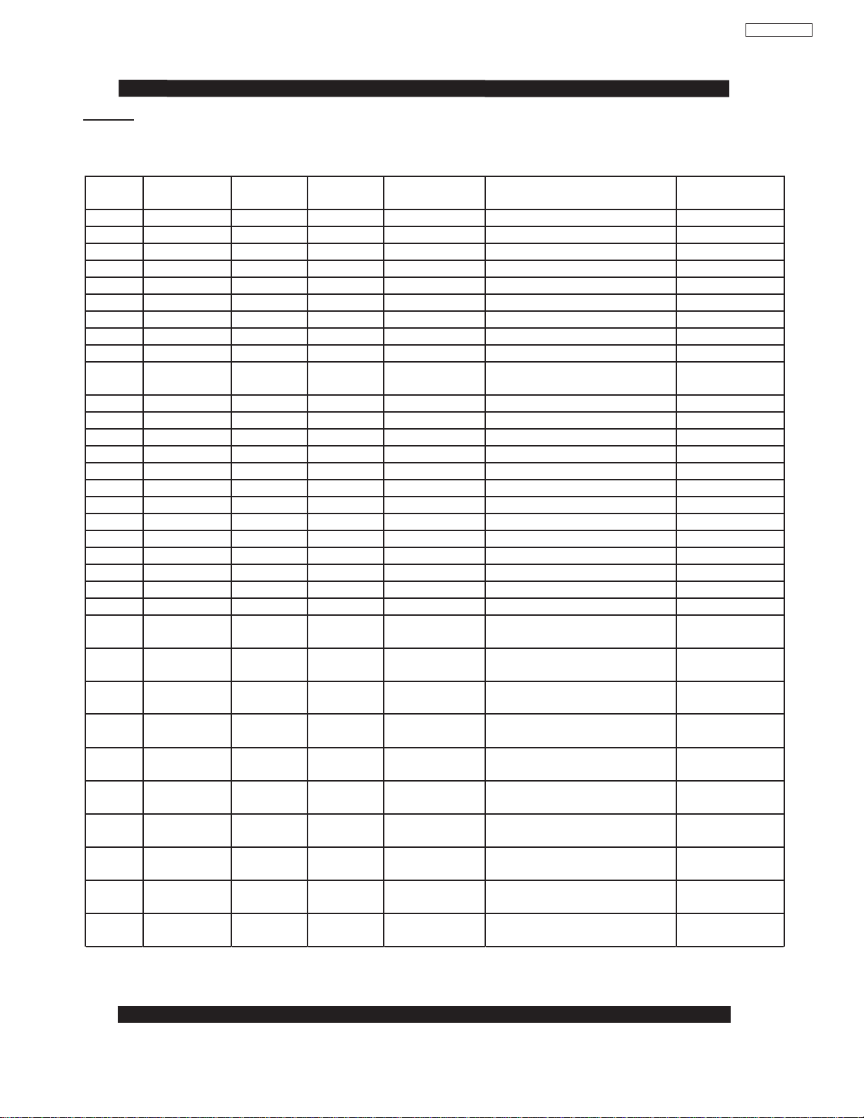
4.5- The following table provides the conversion strings for the “Write” commands
Table 4.5.1 Write Data Command Summary
No.
Item
Command
Initial
Condition
Hex Character
Hex Code Set
Result
1
PowerOn0
6E0000000001
364530303030303030303031
Turns Power On
2
Power
Off
0
6E0000000000
364530303030303030303030
Turns Power Off
3
Input
Input 1
-
6F0000000000
364630303030303030303030
Input 1
4
Input
Input 2
-
6F0000000001
364630303030303030303031
Input 2
5
Input
Input 3
-
6F0000000002
364630303030303030303032
Input 3
6
Input
Input 4
-
6F0000000003
364630303030303030303033
Input 4
7
Input
Input 5
-
6F0000000004
364630303030303030303034
Input 5
8
Input
Antenna A
6F0000000006
364630303030303030303036
Antenna A
9
Input
Antenna B
-
6F0000000007
364630303030303030303037
Antenna B
10
Input
Photo
Input
-
6F0000000009
364630303030303030303039
Photo Input
11
Volume
Set to 0
20
270000000000
323730303030303030303030
Set to 0
12
Balance
Set to 31
30
280000000031
323830303030303030303331
Set to 31
13
Treble
Set to 16
15
2B0000000016
324230303030303030303136
Set to 16
14
Bass
Set to16
15
2A0000000016
324130303030303030303136
Set to 16
15
Audio Mute
Set to off
0
290000000000
323930303030303030303030
Set to Off
16
Audio Mute
Set to On
0
290000000001
323930303030303030303031
Set to On
17
Picture Mode
Set to Day
0
A40000000000
413430303030303030303030
Set to Day
18
Picture Mode
Set to Night
0
A40000000001
413430303030303030303031
Set to Night
19
Contrast
Set to 59
60
590000000059
353930303030303030303539
Set to 59
20
Brightness
Set to 29
30
1F0000000029
314630303030303030303239
Set to 29
21
Color
Set to 29
30
100000000029
313030303030303030303239
Set to 29
22
Tint
Set to 29
30
130000000029
313330303030303030303239
Set to 29
23
Sharpness
Set to 29
30
140000000029
313430303030303030303239
Set to 29
24
Color
Temperature
Set to
High
-
600000000000
363030303030303030303030
Set to
High
25
Color
Temperature
Set to
Medium
-
600000000001
363030303030303030303031
Set to
Medium
26
Color
Temperature
Set to
Standard
-
600000000002
363030303030303030303032
Set to
Standard
27
Color
Temperature
Set to
B&W
-
600000000003
363030303030303030303033
Set to
B&W
28
Aspect Ratio
Set to
16:9 Std.
-
400000000000
343030303030303030303030
Set to Standard
29
Aspect Ratio
Set 16:9
Zoom
-
400000000001
343030303030303030303031
Set 16:9 Zoom
30
Aspect Ratio
Set to 4:3
Standard
-
400000000002
343030303030303030303032
Set to 4:3
Standard
31
Aspect Ratio
Set to 4:3
Expanded
-
400000000003
343030303030303030303033
Set to 4:3
Expanded
32
Aspect Ratio
Set to 4:3
Zoom
-
400000000004
343030303030303030303034
Set to 4:3
Zoom
33
Aspect Ratio
Set to 4:3
Zoom 2
-
400000000005
343030303030303030303035
Set to 4:3
Zoom 2
Figure 7
PW1A
19
Page 20
Plasma TV
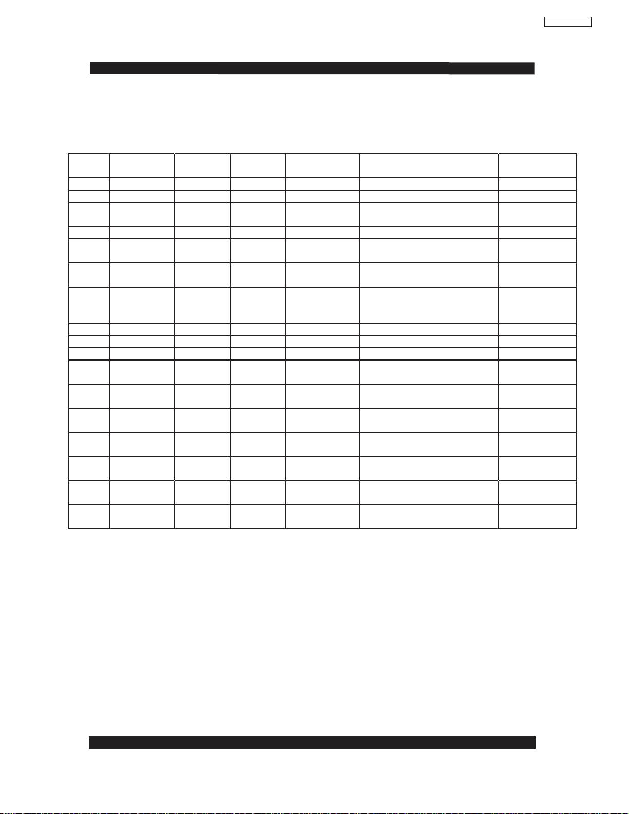
Table 4.5.1 Write Data Command Summary (Continued)
No.
Item
Command
Initial
Condition
Hex Character
Hex Code Set
Result
34
InfoOn0
B20000000001
423230303030303030303031
Turns Info On
35
Info
Off
0
B20000000000
423230303030303030303031
Turns Info Off
36
Direct CH
0~9
Key Code
to 0
-
D00000000000
443030303030303030303030
Key code to 0
37
Direct CH -
CH-
-
D00000010000
443030303030303130303030
CH-
38
Direct CH
Select
Select CH
-
D00000020000
443030303030303230303030
CH Select
39
Auto Movie
Mode
Auto
Movie Off
-
D40000000000
443430303030303030303030
Auto Movie Off
40
Auto Movie
Mode
Auto
Movie On
(Auto)
-
D40000000000
443430303030303030303031
Auto Movie On
(Auto)
(RGB Mode)
41
Contrast
Set to 59
60
590000000059
353930303030303030303539
Set to 59
42
Brightness
Set to 29
30
1F0000000029
314630303030303030303239
Set to 29
43
Color
Temperature
Set to
High
-
600000000000
363030303030303030303030
Set to
High
44
Color
Temperature
Set to
Medium
-
600000000001
363030303030303030303031
Set to
Medium
45
Color
Temperature
Set to
Standard
-
600000000002
363030303030303030303032
Set to
Standard
46
Color
Temperature
Set to
B&W
-
600000000003
363030303030303030303033
Set to
B&W
47
Aspect Ratio
Set to
16:9 Std.
-
400000000000
343030303030303030303030
Set to Standard
48
Aspect Ratio
Set to 4:3
Standard
-
400000000002
343030303030303030303032
Set to 4:3
Standard
49
Aspect Ratio
Set to
Real
-
400000000006
343030303030303030303036
Set to Real
PW1A
20
Page 21
PRECAUTIONS
● How to clean the plasma screen panel of the monitor
Before cleaning the monitor, turn off the monitor and disconnect the power plug from the power outlet.
To prevent scratching or damaging the plasma screen face, do not knock or rub the surface with sharp or
hard objects. Clean the screen with a soft cloth moistened with warm water and dry with a soft cloth. If it is
not enough, then use a cloth with mild detergent. Do not use harsh or abrasive cleaners.
● How to clean the cabinet of the monitor
Use a soft cloth to clean the cabinet and control panel of the monitor. When excessively soiled dilute a neutral detergent in water, wet and wring out the soft cloth and afterward wipe with a dry soft cloth.
Never use acid/alkaline detergent, alcoholic detergent, abrasive cleaner, powder soap, OA cleaner, car wax,
glass cleaner, etc. especially because they would cause discoloration, scratches or cracks.
1. Features
● Large-screen, high-definition plasma display panel
The 42-inch color plasma display panel, with a resolution of 852 (H) x 480(V) pixels, creates a high-definition,
large-screen (aspect ratio : 16:9) and low-profile flat display. Free from electromagnetic interferences from
geomagnetic sources and ambient power lines, the panel produces medium-quality display images free from
color misconvergence and corner focus distortion.
● High Performance Digital Processor
A wide range of personal computer signals can be handled, from 640 x 400, 640 x 480 VGA to 1600 x 1200 UXGA.
(RGB Analog input)
● Easy-to-use remote control and on screen display system (OSD)
The remote control included eases the work of setting display controls. Further, the on-screen display (OSD)
displays the input status control settings in an easy-to-view fashion.
● Power saving system
The International ENERGY STAR power saver feature saves power consumption automatically when
input signals are not available.
When connected to a VESA DPMS-compliant PC, the monitor cuts its power consumption while it is idle.
● TruBass
TruBass, SRS and () symbol are trademarks of SRS Labs,Inc.
TruBass technology is incorporated under license from SRS Labs, Inc.
[AV MONITOR model] CMP420V1A, CMP420V2A
● One mini D-sub terminal and one DVI-D terminal for RGB input.
(The D-sub terminal can also receive component RGB - selectable via customer OSD.)
(One of the component inputs has the capability to select RGB via customer OSD.)
● One composite/S-video input terminal and two component video input terminals, added with VIDEO board.
(It operates as composite/S-video input and RGB input and RGB input terminal, or composite video output terminal.)
● One SCART terminal for EUROPEAN, added with VIDEO board.
● One composite video output terminal as a monitoring output, added with VIDEO board.
● Simple type remote (CP-RD4).
[TELEVISION model] 42EDT41A
● Various input/output terminals added with VIDEO board. (same features as above mentioned AV MONITOR)
● Tuner input added with VIDEO board
● Complex type remote (CLU-W900)
PW1A
21
Page 22
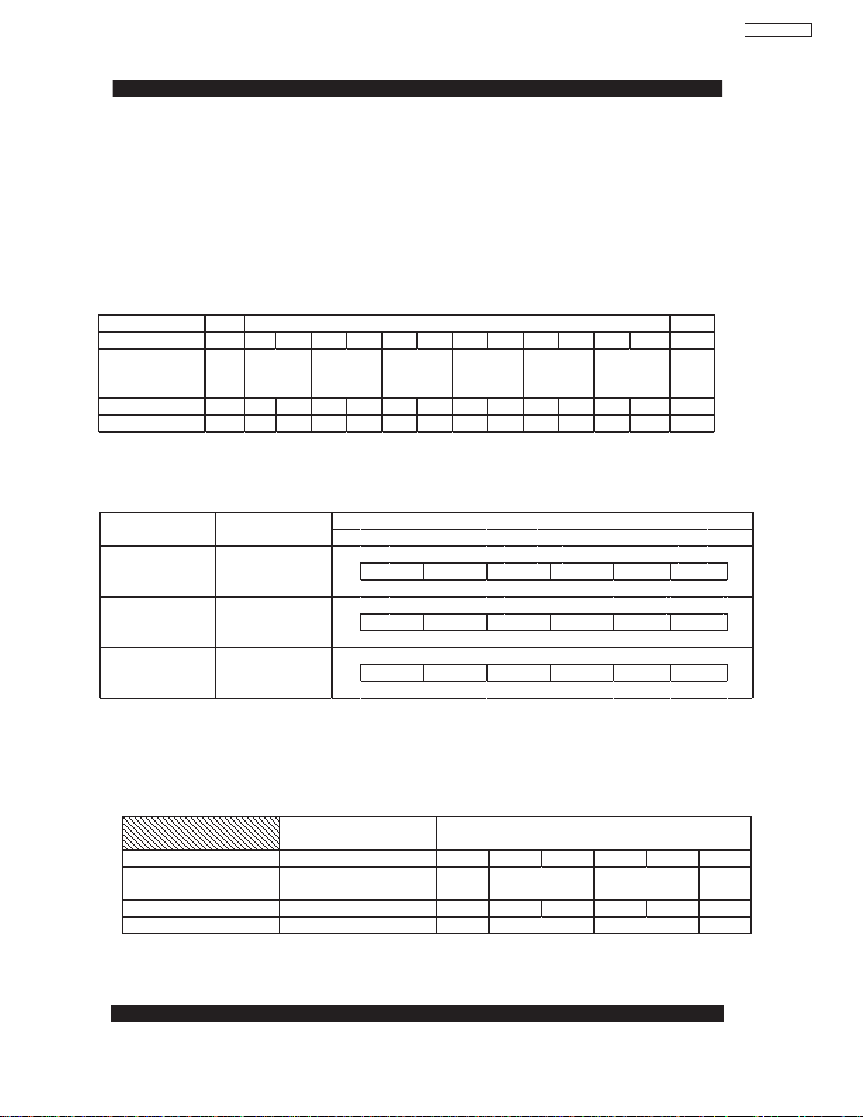
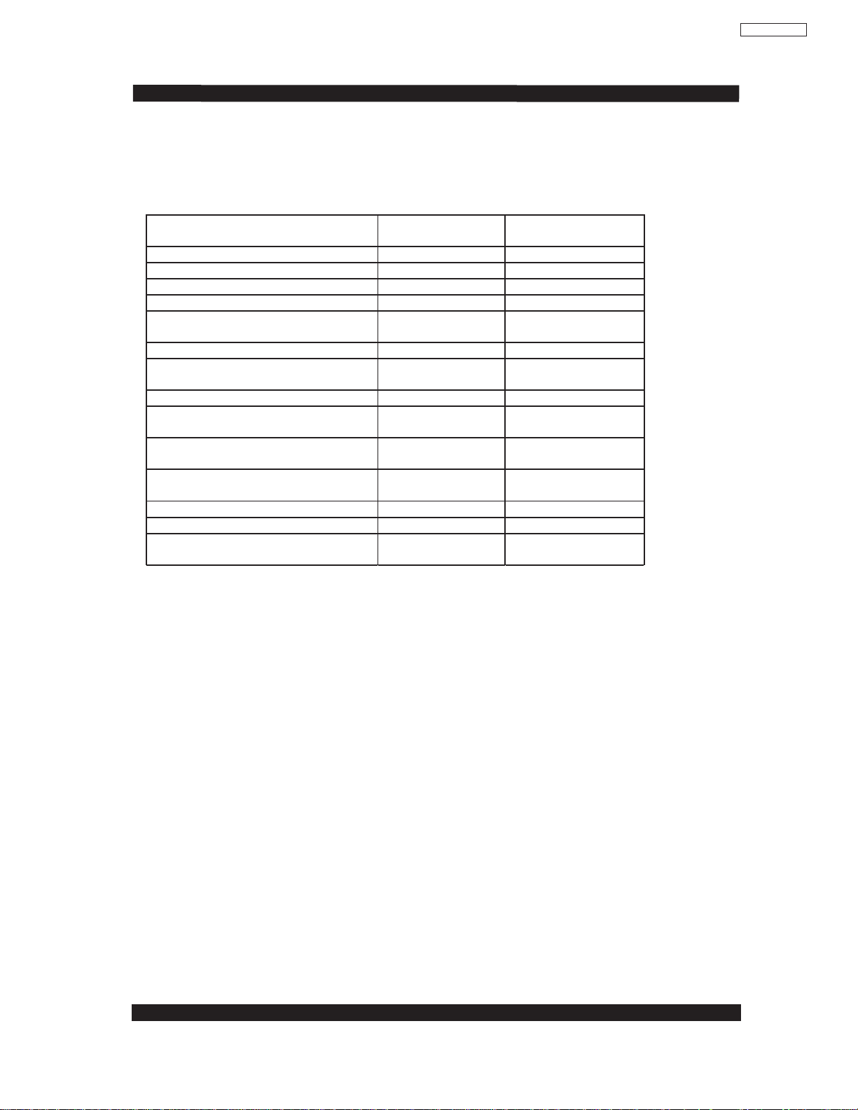
2. Specifications
Panel
Display
dimensions
Approx. 42 inches (920 (H) x 518 (V) mm, diagonal 1059mm)
Resolution
852 (H) x 480 (V) pixels
Net dimensions
(excluding Speakers/Stand)
1030 (W) x 636 (H) x 91 (D) mm
Net weight
(excluding Speakers/Stand)
CMP420V1A/V2A:33.2kg 42EDT41A:34.2kg
Ambient
conditions
Temperature
Relative humidity
Operating : 20% to 80%, Storage : 20% to 90% (non-condensing)
Power supply
AC100 - 240V, 50/60Hz
Power consumption/at standby
310W / <3W
Audio output
(RGB input)
Input signals
Input terminals
RGB1 DVI input terminal (DVI-D)
RGB1 audio input terminal (3.5mm Stereo Mini Jack)
RGB2 analog RGB input terminal (D-sub 15-pin)
RGB2 audio input terminal (3.5mm Stereo Mini Jack)
Video signals
0.7 V/1.0 Vp-p, analog RGB (Recommended Signal)
480i, 576i, 480p, 576p, 1080i/50, 1080i/60, 720p/60
Sync signals
H/V separate, TTL level [2K ]
H/V composite, TTL level [2K ]
Sync on green, 0.3 Vp-p [75 ]
(Video input)
(RF input)
Input signals
Input signals
Input terminals
Input terminals
RF Video System
AV1: composite video input terminal (RCA)
AV1: Y PB PR video input terminal (RCA)
AV1: L/R audio input terminal (RCA)
AV2: composite video input terminal (RCA)
AV2: Y/G PB/B PR/R video input terminal (RCA)
AV2: L/R audio input terminal (RCA)
AV3: composite video input terminal (RCA)
AV3: S video input terminal (RCA)
AV3: L/R audio input terminal (RCA)
AV4: composite video / S video / RGB / L/R audio input terminal (Scart)
Video signals
AV1: NTSC-M, PAL-M, PAL-N
AV1: 480i, 576i, 480p, 576p, 1080i/50, 1080i/60, 720p/60
AV2: NTSC-M, PAL-M, PAL-N
AV2: 480i, 576i, 480p, 576p, 1080i/50, 1080i/60, 720p/60, RGB
AV3: NTSC-M, PAL-M, PAL-N
AV4: NTSC-M, PAL-M, PAL-N
NTSC-M
AV4: RGB
Video output Signal
OUTPUT (MONITOR): composite video monitor-output terminal (RCA)
OUTPUT (MONITOR): L/R audio monitor- output terminal (RCA)
AV4: composite video / L/R audio monitor-output terminal (SCART)
Operating : 5 to 35, Storage : -15 to 60
12W + 12W (6 )
ANT : 75 unbalanced
Applicable video signals for each input terminal
Terminal RCA/SCART DVI D-sub
Signal CVBS S-video Component RGB PC STB RGB Component
AV1
AV2
AV3
AV4
RGB1
RGB2
( :Available)
PW1A
22
Page 23
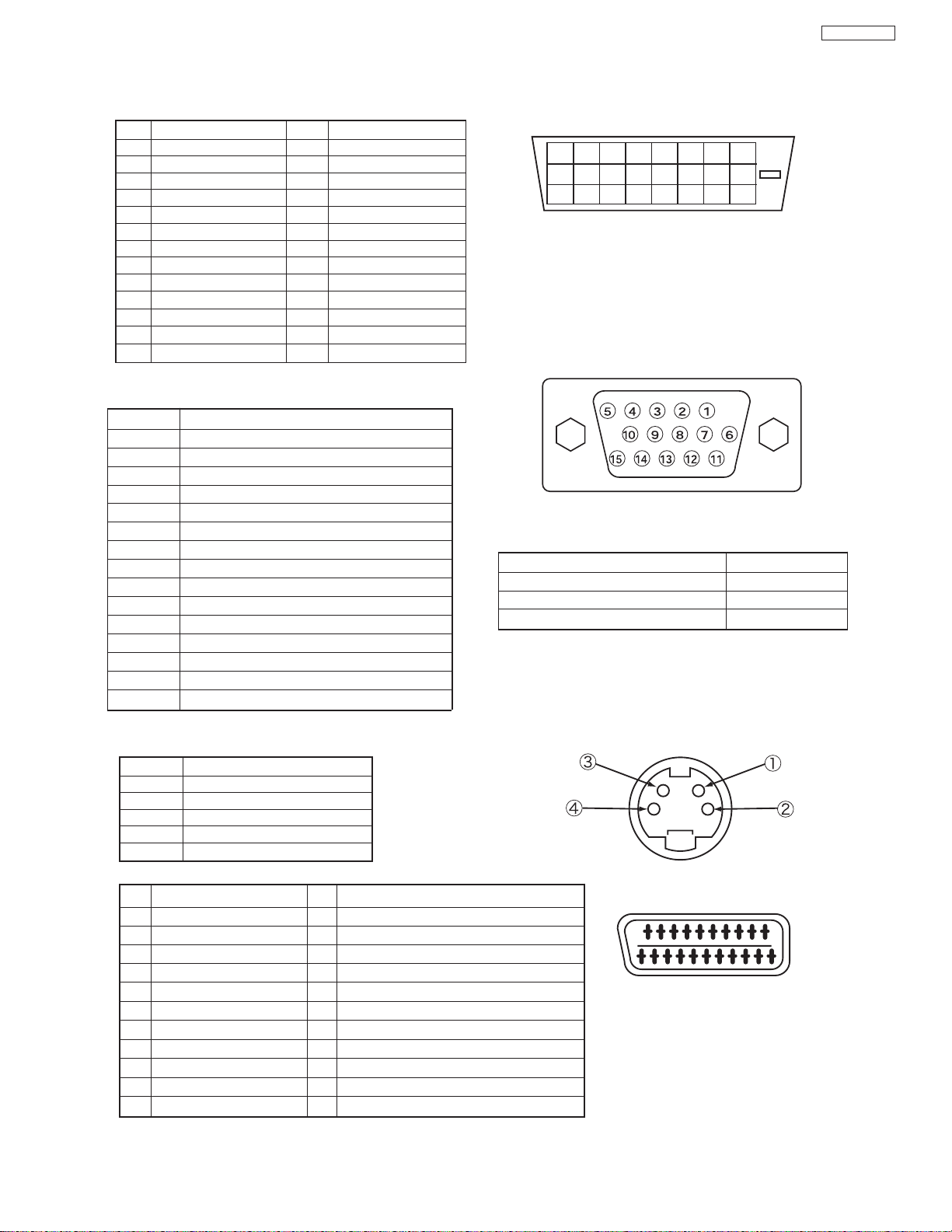
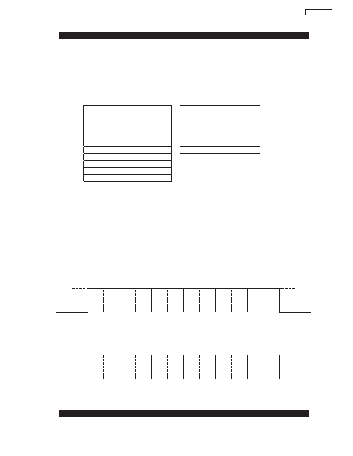
S-input connector pin specifications
Pin Input signal
1 Y
2 Y-GND
3 C
4 C-GND
Frame GND
20 18 16 14 12 10 8 6 4 2
21
19 17
15 13 11 975
31
Scart connector pin specifications
Pin Signal Pin Signal
1
AUDIO OUT (RIGHT)
12
Not Used
2
AUDIO IN (RIGHT)
13
RGB-R GND
3
AUDIO OUT (LEFT/MONO)
14
GND
4
AUDIO GND
15
RGB-R / S.VHS CHROMINANCE IN
5
RGB-B GND
16
BLANKING SIGNAL
6
AUDIO IN (LEFT/MONO)
17
COMPOSITE VIDEO GND
7
RGB-B IN
18
BLANKING SIGNAL GND
8
AUDIO/RGB SWITCH / 16:9
19
COMPOSITE VIDEO OUT
9
RGB-G GND
20
COMPOSITE VIDEO / S.VHS LUMINANCE IN
10
Not Used
21
GND / SHIELD (CHASSIS)
11
RGB-G IN
RGB terminal (D-sub 15-pin connector)
• When different kinds of input signals are simultaneously input to
the monitor via a graphics board or the like, the monitor will
automatically select the signals in the following priority order:
*Even in the case of the recommended signals shown on the
following page, there may be instances when correct display is
not possible. In this case, use H/V separate sync, H/V composite
sync.
Sync signal type Priority
H/V separate sync. 1
H/V composite sync. 2
sync.on Green * 3
Pin
Input signal
1 R (PR/CR)
2 G or sync on green (Y)
3 B (PB/CB)
4 No connection
5 No connection
6 R.GND (PR/CR, GND)
7 G.GND (Y, GND)
8 B.GND (PB/CB, GND)
9 No connection
10 GND
11 No connection
12 [SDA]
13 H. sync or H/V composite sync
14 V.sync. [V.CLK]
15 [SCL]
( ) : With component input
12345678
9 10 11 12 13 14 15 16
17 18 19 20 21 22 23 24
DVI terminal (DVI-D)
Signal Input
Pin Input signal Pin Input signal
1
T.M.D.S. Data2-
14
+5V Power
2
T.M.D.S. Data2+
15
Ground (for+5V)
3
T.M.D.S. Data2/4 Shield
16
Hot Plug Detect
4
T.M.D.S. Data4-
17
T.M.D.S. Data0-
5
T.M.D.S. Data4+
18
T.M.D.S. Data0+
6
DDC Clock
19
T.M.D.S. Data0/5 Shield
7
DDC Data
20
T.M.D.S. Data5-
8
No Connect
21
T.M.D.S. Data5+
9
T.M.D.S. Data1-
22
T.M.D.S. Clock Shield
10
T.M.D.S. Data1+
23
T.M.D.S. Clock+
11
T.M.D.S. Data1/3 Shield
24
T.M.D.S. Clock-
12
T.M.D.S. Data3-
Frame GND
13
T.M.D.S. Data3+
PW1A
23
Page 24
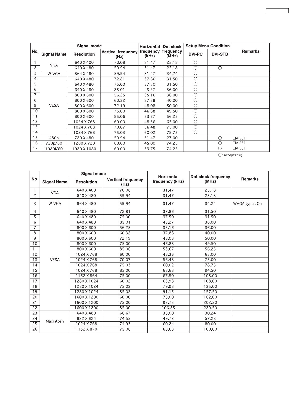
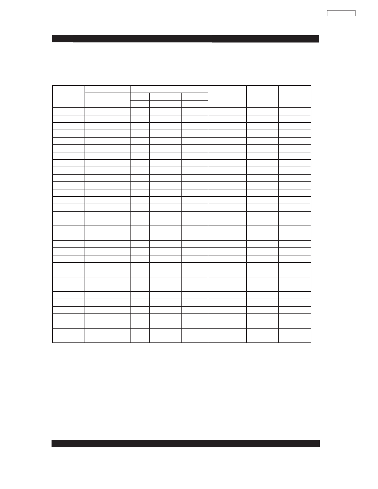
Recommended Signal List
With Digital RGB signal input (RGB1 input)
(
With Analog RGB signal input (RGB2 input)
• Make sure that the signal of the equipment to be connected is compatible with the pecifications of this list.
PW1A
24
Page 25
PW1A
• The type of video board or connecting cable used may not allow for correct displays adjustment of Horizontal Position, Vertical Position, Horizontal
Clock and Clock Phase.
• The monitor may fail to display an animation image correctly when a signal having a vertical frequency of 85Hz or higher is input to it.
• The monitor differentiates the signal modes according to the horizontal and vertical frequencies and the horizontal and vertical sync signal
polarities. Note that different signals having all these elements alike may be handled as the same signal.
• Displaying images with more than 480 lines of vertical resolution at Full diplay (compressed display) can result in the interpolation of stripes.
No.
Signal mode
Horizontal
frequency (kHz)
Dot clock
frequency (MHz)
Remarks
Signal Name Resolution
Vertical frequency
(Hz)
1
NTSC-M
525 59.94 15.73
With Composite Input(AV1~AV4 input) and S-video Input (AV3 and AV4 input).
No.
Signal mode
Horizontal
frequency (kHz)
Dot clock
frequency (MHz)
Remarks
Signal Name Resolution
Vertical frequency
(Hz)
1
(NTSC-M)
525 59.94 15.73
With R, G, B Video input (AV2 and AV4 input).
No.
Signal mode
Horizontal
frequency (kHz)
Dot clock
frequency (MHz)
Remarks
Signal Name Resolution
Vertical frequency
(Hz)
1 576i 576 50.00 15.63
2 480i 480 59.94 15.73
3 576p 576 50.00 31.26
4 480p 480 59.94 31.47
5 1080i/50 1080 50.00 28.13
6 1080i/60 1080 60.00 33.75
7 720p/60 720 59.94 44.96
With component input (AV1, AV2 and RGB2-component input).
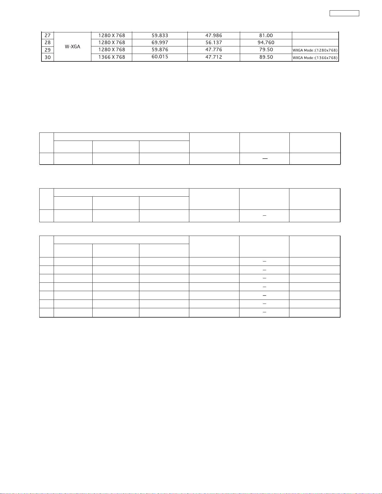
• The monitor differentiates the signal modes according to the horizontal and vertical frequencies and the horizontal and vertical sync signal
polarities. Note that different signals having all these elements alike may be handled as the same signal.
• Displaying images with more than 480 lines of vertical resolution at Full diplay (compressed display) can result in the interpolation of stripes.
25
Page 26
3. Component names
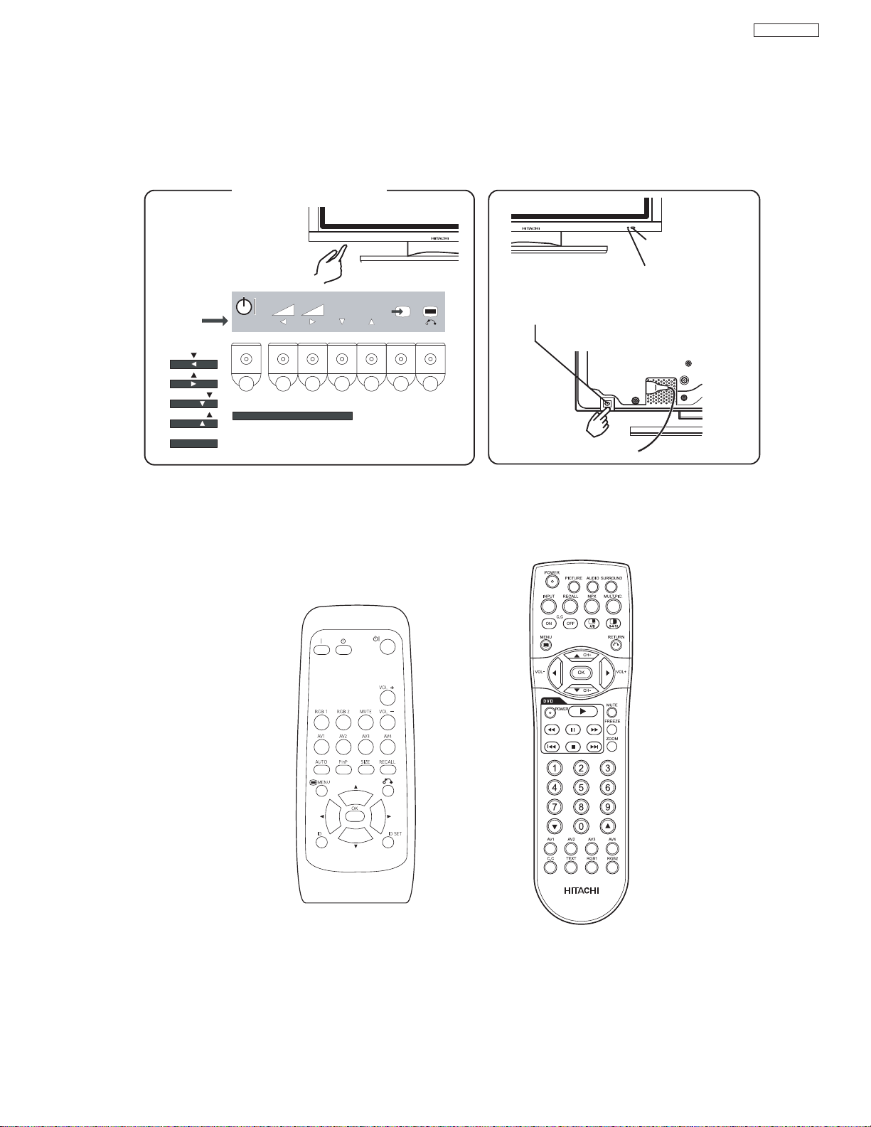
Remote-control
receiver
• Adjustment buttons are located
on the bottom.
• The back cover is provided with
indications to distinguish the
adjustment buttons.
Control panel
Main power switch
• The main power switch is located at the back, on the
lower surface.
Indicating lamp
for
42EDT41A
[Remote control]
[Main unit]
for
CMP420V1A
CMP420V2A
NOTE:
1st number indicates normal button operation
2nd number indicates function during MENU
Rear Label
7654321
- +
OK
2. VOL
2. ADJ
1. SUB POWER
3. VOL
3. ADJ
4. PROGRAM
4. SELECT
5. PROGRAM
5. SELECT
6. INPUT SELECT
6. OK
7. MENU
PW1A
26
Page 27
4. Service points
Lead free solder
This product uses lead free solder (unleaded) to help preserve the environment. Please read these
instructions before attempting any soldering work.
Caution: Always wear safety glasses to prevent fumes or molten solder from getting into the eyes. Lead
free solder can splatter at high temperatures (600˚C).
Lead free solder indicator
Printed circuit boards using lead free solder are engraved with an "F."
Properties of lead free solder
The melting point of lead free solder is 40-50˚C higher than leaded solder.
Servicing solder
Solder with an alloy composition of Sn-3.0Ag-0.5Cu or Sn-0.7Cu is recommended.
Although servicing with leaded solder is possible, there are a few precautions that have to be taken. (Not
taking these precautions may cause the solder to not harden properly, and lead to consequent malfunctions.)
Precautions when using leaded solder
Remove all lead free solder from soldered joints when replacing components.
If leaded solder should be added to existing lead free joints, mix in the leaded solder thoroughly after the
lead free solder has been completely melted (do not apply the soldering iron without solder).
Servicing soldering iron
A soldering iron with a temperature setting capability (temperature control function) is recommended.
The melting point of lead free solder is higher than leaded solder. Use a soldering iron that maintains a high
stable temperature (large heat capacity), and that allows temperature adjustment according to the part being
serviced, to avoid poor servicing performance.
Recommended soldering iron:
Soldering iron with temperature control function (temperature range: 320-450˚C)
Recommended temperature range per part:
Part Soldering iron temperature
Mounting (chips) on mounted PCB 320˚C±30˚C
Mounting (chips) on empty PCB 380˚C±30˚C
Chassis, metallic shield, etc. 420˚C±30˚C
(1) FILTER PWB, SW PWB, LED/RECEIVER PWB, TACT SW PWB, SP TERMINAL(L/R) PWB
(2) AUDIO PWB, JOINT PWB
(3) VIDEO PWB
(4) FORMATTER PWB
(5) POWER BOARD
The PWB assembly which has used lead free solder
PW1A
27
Page 28

CMP420V1 / CMP420V2 / 42EDT41 (PW1A)
5. SERVICE MODE ACCESS
BURN-IN MODE
BURN-IN MODE
When the Burn-in feature is turned ON, the plasma panel operates normally on all inputs that
have a signal. On inputs that do not have a signal, the plasma panel displays a cycling single
color test pattern (see below) which is generated internally. This can be helpful to determine
if the panel is capable of displaying anything.
NOTE:
1st number indicates normal button operation
2nd number indicates function during MENU
Rear Label
7654321
- +
OK
2. VOL
2. ADJ
1. SUB POWER
3. VOL
3. ADJ
4. PROGRAM
4. SELECT
5. PROGRAM
5. SELECT
6. INPUT SELECT
6. OK
7. MENU
1 2 6
BURN-IN MODE (ON)
With unit in standby mode
(turned off), press and hold: >
After the unit comes on, continue to hold the
buttons down until the initial OSD goes
away. OSD will then appear indicating that
BURN-IN MODE is engaged.
(OSD > Burn In On)
1 2
BURN-IN MODE (OFF)
With unit in standby mode
(turned off), press and hold: >
After the unit comes on, continue to hold the
buttons down until the initial OSD goes
away. OSD will then appear indicating that
BURN-IN MODE is disengaged.
(OSD > Burn In Off)
White Yellow Cyan Green Magenta Red Blue Black
7
PW1A
28
Page 29

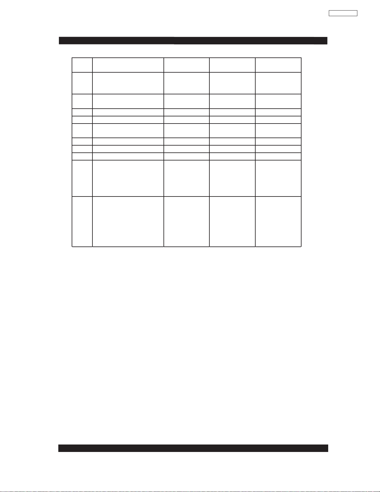
CMP420V1 / CMP420V2 / 42EDT41 (PW1A)
DEMO MODE
When the DEMO feature is turned ON, both the remote and the plasma panel front panel
buttons (with the exception of the SUB POWER button) are non-operational. This can be
useful for the Sales / Dealers to prevent anyone from playing with any of the settings.
NOTE: This is the front panel shortcut to parameter #175 in the I2C ADJUSTMENT MODE.
NOTE:
1st number indicates normal button operation
2nd number indicates function during MENU
Rear Label
7654321
- +
OK
2. VOL
2. ADJ
1. SUB POWER
3. VOL
3. ADJ
4. PROGRAM
4. SELECT
5. PROGRAM
5. SELECT
6. INPUT SELECT
6. OK
7. MENU
DEMO MODE (OFF)
With unit in standby mode
(turned off), press and hold: >
After the unit comes on, continue to hold
the buttons down until the initial OSD goes
away. DEMO MODE is now disengaged,
although you will not see any OSD confirmation.
1 3
DEMO MODE (ON)
With unit in standby mode
(turned off), press and hold: >
After the unit comes on, continue to hold the
buttons down until the initial OSD goes
away. DEMO MODE is now engaged, although you will not see any OSD confirmation.
1 3 6
SERVICE MODE ACCESS
DEMO MODE
PW1A
29
Page 30

CMP420V1 / CMP420V2 / 42EDT41 (PW1A)
I2C ADJUSTMENT MODE
When the set is in the I2C Adjustment mode, use the cursor buttons
for selecting the
adjustment parameter, and for changing the parameterʼs value. Use the OK button to
confirm. After adjustments are complete, press the MENU button to return the set to normal
operating condition.
NOTE:
1st number indicates normal button operation
2nd number indicates function during MENU
Rear Label
7654321
- +
OK
2. VOL
2. ADJ
1. SUB POWER
3. VOL
3. ADJ
4. PROGRAM
4. SELECT
5. PROGRAM
5. SELECT
6. INPUT SELECT
6. OK
7. MENU
I2C Adjustment Mode
With unit in standby mode
(turned off), press and hold: >
After the unit comes on, continue to hold the
buttons down until the initial OSD goes
away. OSD will then appear indicating that
I2C ADJUSTMENT MODE is engaged.
1 4 6
MEMORY INITIALIZATION
Donʼt indiscriminately perform this procedure as it can result in a loss of data if the old values were not recorded.
1. Engage I2C Adjustment mode.
2. Select parameter #744. Change the data value from “0” to “1”.
3. Activate MEMORY INITIALIZATION by holding down the OK button for at least
three seconds.
4. Select parameter #374. Change the data value from “1” to “0”.
5. Check that the set changes input to AV1, indicating that the preset values have been
loaded.
SERVICE MODE ACCESS
I2C ADJUSTMENT MODE
PW1A
30
Page 31

PW1A
CMP420V1 / CMP420V2 / 42EDT41 (PW1A)
FACTORY RESET
Occasionally, it becomes necessary to perform a factory reset. This is different than the
Memory Initialization, only customer settings are affected by Factory Reset.
NOTE:
1st number indicates normal button operation
2nd number indicates function during MENU
Rear Label
7654321
- +
OK
2. VOL
2. ADJ
1. SUB POWER
3. VOL
3. ADJ
4. PROGRAM
4. SELECT
5. PROGRAM
5. SELECT
6. INPUT SELECT
6. OK
7. MENU
Factory Reset
With unit in standby mode
(turned off), press and hold: >
After the unit comes on, continue to hold the
buttons down until the initial OSD goes
away. Factory Reset has now engaged,
although you will not see any OSD confirmation.
1 5 6
SERVICE MODE ACCESS
FACTORY RESET
31
Page 32

CMP420V1 / CMP420V2 / 42EDT41 (PW1A)
1 5
Diagnosis Mode
With unit in standby mode
(turned off), press and hold: >
After the unit comes on, continue to hold the
buttons down until the initial OSD goes
away. OSD will then appear indicating that
the DIAGNOSIS MODE is engaged.
DIAGNOSIS MODE
This chassis has a limited self-diagnosis mode. When activated, the microprocessor generates a series
of internal communication checks and outputs the results via OSD, as seen on the table below. Since
it uses the OSD to display the results, any circuit failures which result in a “no display” or “no picture” condition will not be able to be seen, obviously. ANY operation (volume, channel, menu, input,
etc.) will cause the unit to exit from the Diagnosis mode.
SERVICE MODE ACCESS
DIAGNOSIS MODE
Code Problem Phenomenon Cause
H11* Tuner problem Can not receive the main signal from antenna U101 error
H15 Com posi t e video SW IC problem Can not receive picture and audio - can not change input mode I 201 error
H16 Component video SW IC problem No component picture - can not change input mode I202 error
H31 Color Demodulator IC problem Abnormal color - dark picture I501 error
H32 Sync separator IC problem Unsynchronized picture I601 error
H33 3D Y/C separat or problem Abnormal color - dark picture/no picture I302 error
F63 I2C Bus latch problem Can’t store data settings
SDA3/SCL3
latched up
* Only with units having a tuner circuit
- - -F63F63 - - - - - -
H33: OKH32: OK
H31: OKH16: OK
H15: OKH11: OK
Diagnosis
Most Recent Failure
Codes
Results
PW1A
32
Page 33

PW1A
Service
adjustment items by I
2
C-bus control
O : Should be ad
j
usted
Should be followed
p
revious data
Function
Adj.
No. Adjust Items Mode
24 Black Level(RGB_AMP) TV/VIDEO 254 127
25 Black Level(RGB_AMP) PC 254 127
26 Reference Amplitude(RGB_AMP) TV/VIDEO 254 127
27 Reference Amplitude(RGB_AMP) PC 254 127
28 Display for Max. Amplitude Level Main - 29 Display for Max. Amplitude Level SUB - 30 SUB_CONTRAST(RF) MAIN 15 7
31 SUB_CONTRAST (AV1) MAIN/SUB COMPOSITE mode 15 7
32 SUB_CONTRAST(RF) SUB 15 7
33 SUB_CONTRAST (AV4) MAIN/SUB COMPOSITE mode 15 7
34 SUB_COLOR(VIDEO-PAL/SECAM) MAIN 15 10
35 SUB_COLOR(RF-PAL/SECAM) MAIN 3 8
36 SUB_COLOR(VIDEO-NTSC) MAIN 15 10
37 SUB_COLOR(RF-NTSC) MAIN 15 6
38 SUB_COLOR(VIDEO-PAL/SECAM) SUB 15 10
39 SUB_COLOR(RF-PAL/SECAM) SUB 3 8
40 SUB_COLOR(VIDEO-NTSC) SUB 15 10
41 SUB_COLOR(RF-NTSC) SUB 15 8
46 S_B-Y_ADJ MAIN 15 8
47 S_R-Y_ADJ MAIN 15 8
48 S_B-Y_ADJ SUB 15 8
49 S_R-Y_ADJ SUB 15 8
50 BPF_Q (4.43MHz) MAIN 3 3
51 BPF_f0 (4.43MHz) MAIN 3 1
52 Y_DL (4.5MHz) For Asia MAIN 10 5
53 Y_DL (5.5MHz PAL/NTSC4.43) For Asia MAIN 10 3
54 Y_DL (5.5MHz SECAM) For Asia MAIN 10 0
55 Y_DL (6.0PAL/NTSC4.43) For Asia MAIN 10 9
56 Y_DL (6.0SECAM) For Asia MAIN 10 9
57 Y_DL (VIDEO PAL/NTSC4.43) MAIN 10 6
58 Y_DL (VIDEO SECAM) MAIN 10 8
59 Y_DL (VIDEO NTSC) MAIN 10 6
60 BELL_f0 MAIN 1 0
61 Y_OUT_LEVEL (VIDEO) MAIN 63 13
62 Initialize function for EEPROM of Video PWB board 1 0
63 Y_OUT_LEVEL (TEXT) MAIN 63 0
64 C_OUT_LEVEL (VIDEO) MAIN 63 7
65 Check condition of EEPROM of Video PWB board 0:Normal, 1:Abnormal(Fail or no assembly) 1 66 C_OUT_LEVEL (TEXT) MAIN 63 0
67 Y_OUT_LEVEL (TEXT) SUB 63 12
TUNER
PWB
Changed Component
PDP
PANEL
Maximum
Value
Default
Formatter
PWB
VIDEO
PWB
33
Page 34

PW1A
O : Should be ad
j
usted
Should be followed
p
revious data
Function
Adj.
No. Adjust Items Mode
TUNER
PWB
Changed Component
PDP
PANEL
Maximum
Value
Default
Formatter
PWB
VIDEO
PWB
68 Y_OUT_LEVEL (VIDEO) SUB 63 13
69 Dispersion Time of Sustain current 0: 2 Times, 1: 4 times For Dynamic (Day) mode 1 0
70 C_OUT_LEVEL (TEXT) SUB 63 7
71 C_OUT_LEVEL (VIDEO) SUB 63 7
72 Dispersion Time of Sustain current 0: 2 Times, 1: 4 times For Natural (Night) mode 1 1
73 BPF_Q (4.43MHz) SUB 3 3
74 BPF_f0 (4.43MHz) SUB 3 1
75 Y_DL (4.5MHz) For Asia SUB 10 5
76 Y_DL (5.5MHz PAL/NTSC4.43) For Asia SUB 10 2
77 Y_DL (5.5MHz SECAM) For Asia SUB 10 0
78 Y_DL (6.0PAL/NTSC4.43) For Asia SUB 10 7
79 Y_DL (6.0SECAM) For Asia SUB 10 10
80 Y_DL (VIDEO PAL/NTSC4.43) SUB 10 8
81 Y_DL (VIDEO SECAM) SUB 10 6
82 Y_DL (VIDEO NTSC) SUB 10 5
83 BELL_f0 SUB 1 0
84 C_TRAP_SW (COMB=OFF-PAL/NTSC4.43/NTSC3.58) MAIN 1 0
85 C_TRAP_SW (COMB=OFF-PAL/NTSC4.43/NTSC3.58) SUB 1 0
86 MVM(VIDEO) - 1 0
87 AFC_GAIN (AV00) - 3 0
88 AFC_GAIN (AV1) - 3 0
89 AFC_GAIN (AV2) - 3 0
90 AFC_GAIN (AV3) - 3 0
91 AFC_GAIN (AV4) - 3 0
92 S_INHBT - 1 0
93 S_ID - 1 0
94 S_GP - 3 0
95 S_V_ID - 1 0
96 BELL/HPF - 3 3
97 Cb offset1 MAIN 15 8
98 Cr offset1 MAIN 15 8
99 Cb offset1 SUB 15 8
100 Cr offset1 SUB 15 8
101 Sharpness Gain(VIDEO) PAL MAIN 15 10
102 Sharpness Gain(RF) MAIN 5 8
103 Sharpness EQ(4.5MHz) MAIN 3 1
104 Sharpness EQ(5.5MHz) MAIN 3 1
105 Sharpness EQ(6.0/6.5MHz) MAIN 3 1
106 Sharpness EQ(VIDEO) MAIN 3 1
107 Sharpness f0(VIDEO) PAL MAIN 3 2
108 Sharpness f0(RF) MAIN 3 2
109 Sharpness Gain(VIDEO) PAL SUB 15 9
110 Sharpness Gain(RF) SUB 5 10
111 Sharpness EQ(4.5MHz) SUB 3 1
112 Sharpness EQ(5.5MHz) SUB 3 1
113 Sharpness EQ(6.0/6.5MHz) SUB 3 1
114 Sharpness EQ(VIDEO) SUB 3 1
115 Sharpness f0(VIDEO) PAL SUB 3 2
116 Sharpness f0(RF) SUB 3 2
117 LPF MAIN 1 0
118 LPF SUB 1 0
119 SECAM D-Trap MAIN/SUB 1 1
120 FILTER SW(RF) MAIN 1 0
121 FILTER SW(RF) SUB 1 0
122 NTSC Comb(Comb off) SUB 1 1
123 HS Phase MAIN 1 0
124 HS Phase SUB 1 0
125 P/N ID MAIN 1 0
126 P/N ID SUB 1 0
127 Y/C_SEP_MODE (COMB=OFF-PAL) - 3 0
128 Y-Pf0 - 1 0
129 Y-EQ_GAIN - 3 2
130 Y-EQ/N.C_LIM - 3 0
131 Y-LPF - 1 0
132 V-EMPH_GAIN - 7 3
133 V-EMPH_N.L - 7 3
134 V-EMPH_CORE - 3 1
135 D RANGE - 1 0
136 DY_GAIN MAIN NTSC mode 15 9
34
Page 35

PW1A
O : Should be ad
j
usted
Should be followed
p
revious data
Function
Adj.
No. Adjust Items Mode
TUNER
PWB
Changed Component
PDP
PANEL
Maximum
Value
Default
Formatter
PWB
VIDEO
PWB
137 DC_GAIN MAIN NTSC mode 15 6
138 VAP_GAIN MAIN NTSC mode 75
139 VAP_INV MAIN NTSC mode 31 10
140 YH_CORE MAIN NTSC mode 30
141 YHCGAIN MAIN NTSC mode 1 1
142 CDL MAIN NTSC mode 7 3
143 YNRK MAIN NTSC mode 1 1
144 YNRINV MAIN NTSC mode 1 0
145 YNRLIM MAIN NTSC mode 3 1
146 CNRK 1 1
147 CNRINV 1 0
148 CNRLIM 3 1
149 YPFG 15 10
150 SEPA_LEVEL 480i/576i 3 2
151 SEPA_LEVEL 480p/576p 3 2
152 SEPA_LEVEL 1080i_50 3 2
153 SEPA_LEVEL 1080i_60/720p 3 2
154 AUTO_FM/AM(D11-D8) - 15 2
155 AUTO_FM/AM(D7-D0) - 254 189
156 A2_THRESHOLD(D11-D8) - 15 0
157 A2_THRESHOLD(D7-D0) - 254 112
158 PRE_AM Except 4.5MHz (Except Dual/Stereo mode) 254 17
159 VOL_SCART1 (D15-D8) - 254 115
160 VOL_SCART1 (D7-D5) - 7 0
161 PRE_SCART - 254 31
162 PRE_FM 4.5MHz(JAPAN) 254 34
163 PRE_FM 4.5MHz(Except BTSC-SAP mode) 254 32
164 PRE_FM 4.5MHz(BTSC-SAP) 254 60
165 PRE_FM
4.5MHz(Except KOREA-Dual/Stereo mode)
254 19
166 PRE_FM 4.5MHz(KOREA-Dual/Stereo) 254 34
167 PRE_FM Except 4.5MHz(Except Dual/Stereo mode) 254 17
168 PRE_FM Except 4.5MHz(Dual/Stereo mode) 254 27
169 PRE_NICAM - 254 57
170 Screen Saver-Picture shift amount 0:1pixel 1:2pixel 2:3pixel 2 0
171 Thermo sensor function available or not 0 None,1 Yes 1 0
172 Video Input function available or not at RGB1 & RGB2 mode 0 Not available, 1 Available 1 1
173
Screen Saver-Picture shift direction 0:dia 1:cross 2:up/down 3:left/right
30
174 AUDIO Function available 0:No , 1:Yes 1 1
175 Remote Function available 0:No , 1:Yes 1 1
176 Power Save On/Off Setting at Initialize,Reset and Shipping 0:Change 1: Don't Change20
177
DVI-STB/RGB-COMPONENT Function available 0 NO 1 YES
10
178 Dynamic Backlight function 0:No, 1:Yes For LCD model 1 1
179 ISM Control for WVGA 1 1
180 Terminal Mode Function available 0:Not Available, 1:Available RS232C 1 0
181 Black insert function 0:Not available, 1:Available
For Dynamic mode or Day mode (For LCD model only)
10
182 AGC_LEVEL AGCL ALL Mode 3 0
183 TEXT H sync delay - 127 0
184 TEXT V sync delay - 127 50
185 TEXT_H_POSITION - 254 42
186 TEXT_V_POSITION - 254 38
187 Lower Limits value for Sync Detect of 2ms interval For AFC at TV mode 254 25
188 Upper Limits Value for Sync Detect of 2ms interval For AFC at TV mode 254 40
189 Lower Limits value for Sync Detect of 2ms interval For Free Running at TV mode 254 30
190 Upper Limits Value for Sync Detect of 2ms interval For Free Running at TV mode 254 45
191 Lower Limits value for Sync Detect of 2ms interval For AUTO OFF at TV mode 254 25
192 Upper Limits Value for Sync Detect of 2ms interval For AUTO OFF at TV mode 254 35
193 Lower Limits value for Sync Detect of 2ms interval For Free Running at AV mode 254 30
194 Upper Limits Value for Sync Detect of 2ms interval For Free Running at AV mode 254 45
195 Counting time for discrimination of fV - 31 2
196 Dispersion Time of Sustain current 0: 2 Times, 1: 4 times For PC mode 1 1
197 Counting time for discrimination of SYNC - 31 2
198 Input Source of fV/fH judghment(0:M30625/TA1370) Component Mode 1 0
199 Counting time for discrimination of fV(M30625/TA1370) - 31 2
200 Y_DL (6.5MHz PAL/NTSC4.43) For Asia Main 10 7
201 Y_DL (6.5MHz SECAM) For Asia Main 10 10
202 Y_DL (6.5MHz PAL/NTSC4.43) For Asia Sub 10 4
203 Y_DL (6.5MHz SECAM) For Asia Sub 10 10
204 PDP-BLK ON/OFF 1:ON, 0:OFF 1 0
205 Counting time for discrimination of fH(M30625/TA1370) - 31 2
35
Page 36

PW1A
O : Should be ad
j
usted
Should be followed
p
revious data
Function
Adj.
No. Adjust Items Mode
TUNER
PWB
Changed Component
PDP
PANEL
Maximum
Value
Default
Formatter
PWB
VIDEO
PWB
206 Sharpness f0(L) Sub 3 2
207 NJW1320_OUT1_GAIN VIDEO PWB 1 0
208 NJW1320_OUT2_GAIN VIDEO PWB 1 0
209 Sharpness f0(L') Sub 3 2
210 AFC_GAIN (Except AV00 mode) Except AV00 mode 3 0
211
Recovery to an error of OSC frequency of Ceramic resonator for timer
62 34
212 Brightness Center (CM)
NT2/NT3/HD2/HD3/PAL2/PAL3/HD9/HD10/NT4/PAL4
254 128
213 Brightness Center (CM) HD1/HD4/HD5/HD6/HD7/HD8 254 128
214 Brightness Center (CM) MULTI PICTURE/NT1/PAL1 254 128
215 Reset function of accumulation time for WVGA/LCD Panel 0:Normal 1:Reset 1 0
216 Contrast Center (CM) Except WVGA & LCD TV/VIDEO(AV3/AV4 mode) 254 137
217 Power key function available or not (At Force AVC mode) 0:Available 1:Cannot10
218 Color Center (CM) NT1/NT2/NT4/HD3/HD4/HD6/PAL4 127 85
219 Color Center (CM) PAL1/PAL2/HD8/HD9 127 85
220 Color Center (CM) NT3/HD1/HD2/HD5/PAL3/HD7/HD10 127 85
221 Tint Center (CM) PAL1 254 120
222 Tint Center (CM) NT1/NT2/NT4/HD3/HD4/HD6 254 113
223 Tint Center (CM) PAL2/HD8/HD10/PAL4 254 108
224 Tint Center (CM) NT3/HD1/HD2/HD5/PAL3/HD7/HD9 254 124
225 Center of Sharpness (HV Enhancer Gain for Y) For Europe TV 31 19
226 Center of Sharpness (HV Enhancer Gain for Y) For Europe VIDEO 31 18
227 Center of Sharpness (HV Enhancer Gain for Y) For Europe HD5/HD6 31 11
228 Center of Sharpness (HV Enhancer Gain for Y) For Europe HD1/HD4/HD7/HD8 31 7
229 Center of Sharpness (HV Enhancer Gain for Y) For Europe HD2/HD3/HD9/HD10 31 15
230 Center of Sharpness (HV Enhancer Gain for Y) For Europe NT2/NT3/PAL2/PAL3/NT4/PAL4 31 15
231 Center of Sharpness (HV Enhancer Gain for Y) For Europe TEXT(for split) 31 7
232 Maximum Value of Contrast at REAL/NORMAL mode 254 188
233 Offset Value of Contrast data at SPLIT mode 120 83
234 Offset value of gain for Black Stretch function Except OFF/LOW/HIGH mode 63 33
235 Demonstration [White] 0-3:None,4:0,5:+10W,6:+20W,7:+30W Mode(common) 7 5
236 Demonstration 0:Normal, 1:Peak Mode 1 1
237 Demonstration [Middle] 0:+0W,1:+10W,2:+20W,3:+30W Mode(common) 3 3
238 Demonstration 0:Normal, 1:Peak Mode 1 0
239 Horizontal Enhance TEXT 3 3
240 YNR Input Level at Low level for DVI-STV Mode 1080i-60/1080i-50/720p-60 7 2
241 YNR Input Level at Low level for DVI-STV Mode 480i/480p/576i/576p/VGA 7 2
242 CNR Input Level at Low level for DVI-STV Mode 1080i-60/1080i-50/720p-60 7 2
243 CNR Input Level at Low level for DVI-STV Mode 480i/480p/576i/576p/VGA 7 2
244 Vertical Enhance TEXT 3 3
245 Demonstration Mode 0:(Off), 1:(On) 1 0
246 WVGA sys_state For WVGA 1 0
247 WVGA BRIGHTNESS For WVGA 1 0
248 Enhancer gain of VH for C TEXT 31 0
249 YNR(NR) Input Level RF Mode 7 3
250 YNR Input Level at Low level for AV1-4 Mode VIDEO 7 3
251 YNR Input Level at Low level for AV1-4 Mode NT2/NT3/PAL2/PAL3/NT4/PAL4 7 3
252 YNR Input Level at Low level for AV1-4 Mode HD1/HD4/HD5/HD6/HD7/HD8 7 3
253 YNR Input Level at Low level for AV1-4 Mode HD2/HD3/HD9/HD10 7 3
254 CNR Input Level at Low level for AV1-4 Mode VIDEO 7 3
255 CNR Input Level at Low level for AV1-4 Mode NT2/NT3/PAL2/PAL3/NT4/PAL4 7 3
256 CNR Input Level at Low level for AV1-4 Mode HD1/HD4/HD5/HD6/HD7/HD8 7 3
257 CNR Input Level at Low level for AV1-4 Mode HD2/HD3/HD9/HD10 7 3
258 Heat APC function (HAPC) available 1 1
261 Select for APC function 1 0
262 "CCFMD" function TV/VIDEO 1 0
263 "CCFMD" function DVI-PC/DVI-STB/DSUB-RGB 1 0
264 NTSC/EBU(CCFORM)
NT1/NT2/HD3/HD4/HD6/HD8/HD10/PAL1/PAL2
10
265 NTSC/EBU(CCFORM)
TV/VIDEO/NT3,4/PAL3,4/HD1,2,5,7,9
10
266 NTSC/EBU(CCFORM) DVI-PC/DVI-STB/DSUB-RGB 10
267 Correction for Tracking (DCBON) TV/VIDEO-Color Temp. : COOL 1 0
268 Correction for Tracking (DCBON) TV/AV-Col. Temp. : Nor/War 1 1
269 Correction for Tracking (DCBON) DVI-PC/DVI-STB/DSUB-RGB 1 1
270 Color Temp. Correction 3 2
271 Typical Value of Contrast OSD DYNAMIC 31 31
272 PC Power Save function (0:Impossible 1:Possible) 1 1
273 Waite Time for POWER SAVE function (s) VIDEO/PC 254 15
274 Lower Limits value for Sync Detect of 2ms interval For Power Save at AV mode 254 5
36
Page 37

PW1A
O : Should be ad
j
usted
Should be followed
p
revious data
Function
Adj.
No. Adjust Items Mode
TUNER
PWB
Changed Component
PDP
PANEL
Maximum
Value
Default
Formatter
PWB
VIDEO
PWB
275 Upper Limits Value for Sync Detect of 2ms interval For Power Save at AV mode 254 200
276 Horizontal Position of OSD 60Hz 15 7
277 Vertical Position of OSD 60Hz 15 7
278 PinP Function 0:PinP, 1:Infomation1, 2:Infomaiton Split 2 0
279 Select for WIDE Mode 1 1
280 Temperature for Fun start (Temp_High) 254 58
281 Temperature for Fun stop (Temp_Low) 254 55
282 Display of internal temperature °C(Temperature) 125 283 Display of Panel map version 255 284 accumulation time for Panel (hours) 65535 285 Initialize function 0:Keep data, 1:Initialize
No.0-No.23,30-33,42-45,289,293,294,741-743
1286 L standard PLL gating HIGH [Europe model] 1 0
287 Select for APC output [Except Europe model] Main FE 2 1
288 Q mode 0:Freeze, 1:Move 1, 2:Move 2 50Hz 2 1
290 AGC adjustment (MFE) [Europe model] MAIN 63 20
291 AGC INPUT(MFE) MAIN - 292 Q mode 0:Freeze, 1:Move 1, 2:Move 2 70Hz(PC) 2 0
293 SUB CONTRAST AV2 MAIN/SUB COMPOSITE mode 15 8
294 SUB CONTRAST AV3 MAIN/SUB COMPOSITE mode 15 8
295 Contrast Center (CM) Except WVGA & LCD AV2 254 137
296 Contrast Center (CM) Except WVGA & LCD AV1 254 137
297 Brightness center (CM) offset AV2 254 127
298 Brightness center (CM) offset AV1 254 127
299 Q mode 0:Freeze, 1:Move 1, 2:Move 2 60Hz 2 1
300 3D ON/OFF 0:ON,1:OFF(Through) 1 0
301 Input Select of TA1370 0:HD1/VD1,1:HD3/VD3 Main/Sub 1 0
302 Sharpness Gain(RF/NR) Main/Sub 15 3
303 3Line Y/C Main- Sub SW 0:Main, 1: Sub 1 0
304 Offset Value(+/-) of Upper Limit (for TB1274:SUB-CONT) Single Picture mode 18 2
305 Offset Value(+/-) of Upper Limit (for FC :RGB-AMP ) Multi Picture mode182
306 Reference Amplitude(RGB_AMP) Multi Picture mode 254 90
307 Component Frq.(fH) Setup (0:28/31/33/45KHz,1:28/31/45KHz) 1 0
308 Terget value of White peak Adj. Single Picture mode 237 235
309 Sharpness Gain(S VIDEO) Main 15 7
310 Sharpness Gain(S VIDEO) Sub 15 7
311 Select color control (0: Asia, 1: South America) Main/Sub 1 0
312 Sharpness Gain Main(N-PAL) 15 8
313 Sharpness f0 Main(N-PAL) 3 2
314 Sharpness Gain Sub (N-PAL) 15 9
315 Sharpness f0 Sub (N-PAL) 3 2
316 Delay Time ON/OFF for Lipsync circuit 0:Off, 1:On 1 1
317 Sync Mode SW 7 0
318
Set Sound System at Auto mode of Sound Sys. (0:auto,1:4.5MHz)
Main 1 0
319
Power condition at power save mode of PC mode after done RESET function 0:Keep last condition, 1:Return to normal condition
10
320
Switch to North USA model from Europe software. OSD change (Wide Mode,...)
0:For Europe, 1:Foe USA (DAY/NIGHT,...)
10
321 Count Souce for ON/OFF Timer 0:MCU-250ms, 1:AC-50/60Hz 1 0
322
Select Wide mode for Europe model (Normal= 5mode/ For Service= 10 mode)
0:Normal, 1:For service10
323 Forced AVC type available 0:Normal type , 1: Forced AVC type 1 0
324 Sharpness Gain Main(M-PAL) 15 8
325 Sharpness f0 Main(M-PAL) 3 2
326 Sharpness Gain Sub (M-PAL) 15 9
327 Sharpness f0 Sub (M-PAL) 3 2
328 CNR Input Level at Low level for Dsub Comp. Mode NT2/NT3/PAL2/PAL3/NT4/PAL4 7 2
329 CNR Input Level at Low level for Dsub Comp. Mode HD1/HD4/HD5/HD6/HD7/HD8 7 2
330 CNR Input Level at Low level for Dsub Comp. Mode HD2/HD3/HD9/HD10 7 2
331 Sharpness Gain(VIDEO) NTSC3.58 MAIN 15 12
332 Sharpness f0(VIDEO) NTSC3.58 MAIN 3 2
333 Sharpness Gain(VIDEO) NTSC3.58 SUB 15 10
334 Sharpness f0(VIDEO) NTSC3.58 SUB 3 2
335 Sharpness Gain(VIDEO) SECAM,B/W MAIN 15 10
336 Sharpness f0(VIDEO) SECAM,B/W MAIN 3 2
337 Sharpness Gain(VIDEO) SECAM,B/W SUB 15 8
338 Sharpness f0(VIDEO) SECAM,B/W SUB 3 2
339 Sharpness Gain(VIDEO) NTSC4.43 MAIN 15 9
340 Sharpness f0(VIDEO) NTSC4.43 MAIN 3 2
341 Sharpness Gain(VIDEO) NTSC4.43 SUB 15 8
342 Sharpness f0(VIDEO) NTSC4.43 SUB 3 2
343 Brightness Limitted Function of PANEL [APSON] 1 1
37
Page 38

PW1A
O : Should be ad
j
usted
Should be followed
p
revious data
Function
Adj.
No. Adjust Items Mode
TUNER
PWB
Changed Component
PDP
PANEL
Maximum
Value
Default
Formatter
PWB
VIDEO
PWB
344 VsVa WAIT TIMER [RISTIM] 15 5
345 Initial value of Contrast Panel life -Extend1 127 93
346 Interval time of correction time Panel life -Extend1 127 10
347 Additional value of Contrast Panel life -Extend1 127 1
348 Initial value of Contrast Panel life -Extend2 127 63
349 Interval time of correction time Panel life -Extend2 127 6
350 Additional value of Contrast Panel life -Extend2 127 1
351 L_PLL.GAIN 1 0
352 AS[YHECLPL0_P0] RF/Multi 15 2
353 AS[YHECLPL1_P0] NT1-except RF/PAL1-except RF 15 2
354 [YHECLPL2_P0] HD 15 1
355 AS[YHECLPL3_P0] NT2,3,4/PAL2,3,4 15 10
356 SEPA_LEVEL_DSUB 480i/576i 3 2
357 SEPA_LEVEL_DSUB 480p/576p 3 2
358 SEPA_LEVEL_DSUB 1080i_50 3 2
359 SEPA_LEVEL_DSUB 1080i_60/720p 3 2
360 HD-PHASE_DSUB 480i/576i 63 20
361 HD-PHASE_DSUB 480p/576p 63 20
362 HD-PHASE_DSUB 1080i_50 63 20
363 HD-PHASE_DSUB 1080i_60/720p 63 20
364 Y_DL (L) MAIN 10 4
365 Y_DL (L') MAIN 10 4
366 Y_DL (L) Sub 10 1
367 Y_DL (L') Sub 10 1
368 Sharpness Gain(L) MAIN 15 10
369 Sharpness Gain(L') MAIN 15 10
370 Sharpness Gain(L) SUB 15 8
371 Sharpness Gain(L') SUB 15 8
372 Sharpness f0(L) MAIN 3 2
373 Sharpness f0(L') MAIN 3 2
374 BURN-IN enable/ disenable 0:Disenable, 1:Enable 1 1
375 BURN-IN mode 2 2
376 CM_THRESHOLD (D15-D8) - 254 0
377 CM_THRESHOLD (D7 -D0) - 254 36
378 Sharpness Gain(RF M) MAIN 15 11
379 Sharpness Gain(RF M) Sub 15 11
380 Sharpness f0 (RF M) Main 3 2
381 Sharpness f0 (RF M) SUB 3 2
382 Counting value of 2ms Sync.Detect MAIN - 383 Counting value of 2ms Sync.Detect SUB - 384 TB1274 Read Data(00h) Main - 385 TB1274 Read Data(01h) Main - 386 TB1274 Read Data(00h) Sub - 387 TB1274 Read Data(01h) Sub - 388 MSP Read Data (CNTROL ) (D15-D8 ) - 389 MSP Read Data (CNTROL ) (D7 -D0 ) - 390 MSP Read Data (STANDARD_RES) (D15-D8 ) - 391 MSP Read Data (STANDARD_RES) (D7 -D0 ) - 392 MSP Read Data (STATUS ) (D15-D8 ) - 393 MSP Read Data (STATUS ) (D7 -D0 ) - 394 TA1370G Read Data(00h) Video board side - 395 TA1370G Read Data(01h) Video board side - 396 TA1370G Read Data(00h) Formater side - 397 TA1370G Read Data(01h) Formater side - 398 uPD64084 Read Data(00H) - 399 uPD64084 Read Data(01h) - 400 Language (Refer to below) 6 0
401 Hotel Mode(0:No,1:Yes) 1 0
402 Analog Data (0:Keep EEPROM,1:Not Keep to EEPROM) 1 0
403 Maximum Volume Limit 63 63
404 Power Mode(0:Last mode, 1:Pos1, 2:V1, 3:V2, 4:V3, 5:V4) 5 0
405 Channel Select(0:CCIR, 1:CHINA) 1 0
406 Auto_sound 4.5 (0:Korea, 1:BTSC, 2:Japan) 2 0
407 T/TEXT(0: None, 1:Yes) 1 1
408 TEXT Language 7 0
409 IIC BUS Data/Clock Open(0:Close, 1:Open) 1 0
410
Channel Preset(0:VESTEL, 1:GIFU, 2:HAMA, 3:HFDM,4:AUSTRALIA)
41
411
Detect and Displsy Tele-Cinema (0:normal 1:Tele Cinema)
--
412 V FREQ 60Hz Force (0:None, 1:Yes) Main/Sub 1 0
38
Page 39

PW1A
O : Should be ad
j
usted
Should be followed
p
revious data
Function
Adj.
No. Adjust Items Mode
TUNER
PWB
Changed Component
PDP
PANEL
Maximum
Value
Default
Formatter
PWB
VIDEO
PWB
413
COLOR SYSTEM CONTROL-MODE(0:BW, 2:3.58NTSC, 3:4.43NTSC, )
Main - 414
COLOR SYSTEM CONTROL-MODE(0:BW, 2:3.58NTSC, 3:4.43NTSC, )
Sub - 415 Horizontal Filter SW [HHPF0] NTSC 1 0
416 Enhancer Gain [HHPF1] PAL 1 0
417 Enhancer Gain [HHPF2] HD 1 0
418 Horizontal Coring Level(Enhancer Gain) AS[HECOR0_PO] NT1-RF 15 1
419 Horizontal Coring Level(Enhancer Gain) AS[HECOR1_PO] PAL1-RF/multi 15 1
420 Horizontal Coring Level(Enhancer Gain) [HECOR2_PO] NT1-Video 15 1
421 Horizontal Coring Level(Enhancer Gain) [HECOR3_PO] PAL1-Video 15 1
422 Horizontal Coring Level(Enhancer Gain) [HECOR4_PO] NT2/NT3/NT4/PAL2/PAL3/PAL4 15 0
423 Horizontal Coring Level(Enhancer Gain) [HECOR5_PO] HD2/HD3/HD9/HD10 15 1
424 Horizontal Coring Level(Enhancer Gain) [HECOR6_PO] HD1/HD4/HD5/HD6/HD7/HD8 15 0
425 Horizontal Coring Level(Enhancer Gain) [HECORPC_PO] PC 15 1
426 Horizontal Coring Level(Enhancer Gain) EU[HECORE_PO] PAL1-RF/multi 15 1
427 Vertical Coring Level(Enhancer Gain) AS[VECOR0_PO] NT1-RF 15 1
428 Vertical Coring Level(Enhancer Gain) AS[VECOR1_PO] PAL1-RF/multi 15 1
429 Vertical Coring Level(Enhancer Gain) [VECOR2_PO] NT1-Video 15 1
430 Vertical Coring Level(Enhancer Gain) [VECOR3_PO] PAL1-Video 15 1
431 Vertical Coring Level(Enhancer Gain) [VECOR4_PO] NT2/NT3/NT4/PAL2/PAL3/PAL4 15 0
432 Vertical Coring Level(Enhancer Gain) [VECOR5_PO] HD2/HD3/HD9/HD10 15 0
433 Vertical Coring Level(Enhancer Gain) [VECOR6_PO] HD1/HD4/HD5/HD6/HD7/HD8 15 0
434 Vertical Coring Level(Enhancer Gain) [VECORPC_PO] PC 15 0
435 Vertical Coring Level(Enhancer Gain) EU[VECORE_PO] PAL1-RF/multi 15 0
436 Horizontal Coring Level(Enhancer Gain) AS[HECOR0_P1] NT1-RF 15 1
437 Horizontal Coring Level(Enhancer Gain) AS[HECOR0_P2] PAL1-RF/multi 15 1
438 Horizontal Coring Level(Enhancer Gain) [HECOR0_P3] NT1-Video 15 1
439 Horizontal Coring Level(Enhancer Gain) [HECOR0_P4] PAL1-Video 15 1
440 Horizontal Coring Level(Enhancer Gain) [HECOR0_P5] NT2/NT3/NT4/PAL2/PAL3/PAL4 15 0
441 Horizontal Coring Level(Enhancer Gain) [HECOR0_P6] HD2/HD3/HD9/HD10 15 1
442 Horizontal Coring Level(Enhancer Gain) [HECOR0_P7] HD1/HD4/HD5/HD6/HD7/HD8 15 0
443 Horizontal Coring Level(Enhancer Gain) [HECORPC_P1] PC 15 1
444 Horizontal Coring Level(Enhancer Gain) EU[HECORE_P1] PAL1-RF/multi 15 1
445 Vertical Coring Level(Enhancer Gain) AS[VECOR0_P1] NT1-RF 15 1
446 Vertical Coring Level(Enhancer Gain) AS[VECOR0_P2] PAL1-RF/multi 15 1
447 Vertical Coring Level(Enhancer Gain) [VECOR0_P3] NT1-Video 15 1
448 Vertical Coring Level(Enhancer Gain) [VECOR0_P4] PAL1-Video 15 1
449 Vertical Coring Level(Enhancer Gain) [VECOR0_P5] NT2/NT3/NT4/PAL2/PAL3/PAL4150
450 Vertical Coring Level(Enhancer Gain) [VECOR0_P6] HD2/HD3/HD9/HD10 15 0
451 Vertical Coring Level(Enhancer Gain) [VECOR0_P7] HD1/HD4/HD5/HD6/HD7/HD8 15 0
452 Vertical Coring Level(Enhancer Gain) [VECORPC_P1] PC 15 0
453 Vertical Coring Level(Enhancer Gain) EU[VECORE_P1] PAL1-RF/multi 15 0
454 YFRNR Input Gain (Main) 2pictures [MYNRG0] except HD-HD 7 1
455 HD-NTSC,HD-PAL(sub)[MYNRG1] HD-HD 7 4
456 4pictures[MYNRG2] NT-*/PAL-* 7 1
457 [MYNRG3] HD-* 7 4
458 YFRNR Input Gain(Sub) [YCNRG0] 2pictures 7 4
459 [YCNRG1] 4pictures/12pictures 7 1
460 CFRNR Input Gain 8Main) 2pictures [MCNRG0] except HD-HD 7 3
461 <HD-NTSC,HD-PAL(Sub) [MCNRG1] HD-HD 7 4
462 [MCNRG2] 7 4
463 [MCNRG3] HD-* 7 4
464 CFRNR Input Gain [SCNRG0] 2pictures 7 3
465 [SCNRG1] 4pictures/12pictures 7 4
466 YFRNR Transition Level [MYNRP0] NT1/PAL1/multi 7 1
467 [MYNRP5] NT1/PAL1-Video 7 0
468 [MYNRP6] NT2/NT3/NT4/PAL2/PAL3/PAL4 7 0
469 [MYNRP7] HD2/HD3/HD9/HD10 7 0
470 [MYNRP8] HD1/HD4/HD5/HD6/HD7/HD8 7 0
471 YFRNR Transition Level (Main/Sub) [MCNRP0] NT1/PAL1/multi 7 2
472 [MCNRP5] NT1/PAL1-video 7 2
473 [MCNRP6] NT2/NT3/NT4/PAL2/PAL3/PAL472
474 [MCNRP7] HD2/HD3/HD9/HD10 7 2
475 [MCNRP8] HD1/HD4/HD5/HD6/HD7/HD8 7 0
476 Vertical Enhancer [YVEG0_P0] NTSC/PAL(-except RF) 15 8
477 [YVEG1_P0] HD2/HD3/HD9/HD10 15 12
478 [YVEG2_P0] HD1/HD4/HD5/HD6/HD7/HD8 15 8
479 AS[YVEG3_P0] PAL1-RF/multi 15 8
480 EU[YVEG0_E_P0] PAL1-RF/multi 15 8
481 Vertical RGB Gain For Y/G [YVDSBG0_P0] NTSC/PAL/multi30
39
Page 40

PW1A
O : Should be ad
j
usted
Should be followed
p
revious data
Function
Adj.
No. Adjust Items Mode
TUNER
PWB
Changed Component
PDP
PANEL
Maximum
Value
Default
Formatter
PWB
VIDEO
PWB
482 [YVDSBG1_P0] HD2/HD3/HD9/HD10 3 0
483 [YVDSBG2_P0] HD1/HD4/HD5/HD6/HD7/HD8 3 0
484 Vertical RGB Coring For Y/G [YVDSBG0_P0] NTSC/PAL/multi 7 0
485 [YVDSBG1_P0] HD 7 3
486 Vertical Enhancer Clip for Y/G [YVECLP0_P0] NTSC/PAL/multi11
487 [YVECLP1_P0] HD 1 1
488 Vertical Clip Offset level [YVECLP0_P0] NTSC/PAL/multi 15 7
489 [YVECLP1_P0] HD 15 1
490 Vertical Non Linear Peaking for Y/G [YVNLP0_P0] NTSC/PAL/multi 63 0
491 [YVNLP1_P0] HD 63 0
492 Horizontal HPF Peak Freq SW for Y/G [YHHPF0_P0] NTSC/PAL/multi 3 2
493 [YHHPF1_P0] HD2/HD3/HD9/HD1031
494 [YHHPF2_P0] HD1/HD4/HD5/HD6/HD7/HD8 3 1
495 Horizontal Enhancer Gain for Y/G [YHEG0_P0] NTSC/PAL(except -RF) 15 15
496 [YHEG1_P0] HD2/HD3/HD9/HD10 15 15
497 [YHEG2_P0] HD1/HD4/HD5/HD6/HD7/HD8 15 0
498 AS[YHEG3_P0] PAL1-RF/multi 15 15
499 EU[YHEG0_E_P0] PAL1-RF/multi 15 15
500 Hrozontal DSB Gain for Y/G [YHDSBG0_P0] NTSC/PAL/multi 3 3
501 [YHDSBG1_P0] HD2/HD3/HD9/HD10 3 0
502 [YHDSBG2_P0] HD1/HD4/HD5/HD6/HD7/HD8 3 0
503 Horizontal DSB Coring for Y/G [YHDSBC0_P0] NTSC/PAL/multi71
504 [YHDSBC1_P0] HD 7 0
505 Horizontal Enhancer Clip for Y/G [YHECLP0_P0] NTSC/PAL/multi10
506 [YHECLP1_P0] HD 1 0
507 Horizontal Clip Offset Level for Y/G AS[YHECLPL0_P0] RF/multi 15 2
508 AS[YHECLPL1_P0] NT1-except RF/PAL1-except RF 15 2
509 [YHECLPL2_P0] HD 15 1
510 EU[YHECLPL0_E_P0] RF/multi 15 4
511 EU[YHECLPL1_E_P0] NT1-except RF/PAL1-except RF 15 4
512 Horizontal Non Linear Peaking for Y/G [YHNLP0_P0] NTSC/PAL/multi 63 0
513 [YHNLP1_P0] HD 63 0
514 Coring Amplitude for Y/G [YCOR0_PO] NT1-RF/PAL1-RF/multi 7 7
515 [YCOR1_PO] NT1-Video/PAL1-Video 75
516 [YCOR2_PO] NT2/NT3/NT4/PAL2/PAL3/PAL473
517 [YCOR3_PO] HD2/HD3/HD9/HD10 7 1
518 [YCOR4_PO] HD1/HD4/HD5/HD6/HD7/HD8 7 1
519 Vertical Enhancer Gain for Y/G [YVEG0_P1] NTSC/PAL(-RF ) 15 8
520 [YVEG1_P1] HD2/HD3/HD9/HD10 15 12
521 [YVEG2_P1] HD1/HD4/HD5/HD6/HD7/HD8 15 8
522 AS[YVEG3_P1] PAL1-RF/multi 15 8
523 EU[YVEG0_E_P1] PAL1-RF/multi 15 8
524 Vertical DSB Gain for Y/G [YVDSBG0_P1] NTSC/PAL/multi30
525 [YVDSBG1_P1] HD2/HD3/HD9/HD10 3 0
526 [YVDSBG2_P1] HD1/HD4/HD5/HD6/HD7/HD8 3 0
527 Vertical DSB Coring for Y/G [YVDSBC0_P1] NTSC/PAL/multi70
528 [YVDSBC1_P1] HD 7 3
529 Vertical Enhancer Clip for Y/G [YVECLP0_P1] NTSC/PAL/multi11
530 [YVECLP1_P1] HD 1 1
531 Vertical Clip Offset Level for Y/G [YVECLP0_P1] NTSC/PAL/multi157
532 [YVECLP1_P1] HD 15 1
533 Vertical Non Linear Peaking for Y/G [YVNLP0_P1] NTSC/PAL/multi630
534 [YVNLP1_P1] HD 63 0
535 Horizontal HPF Pead Freq SW for Y/G [YHHPF0_P1] NTSC/PAL/multi 3 2
536 [YHHPF1_P1] HD2/HD3/HD9/HD1031
537 [YHHPF2_P1] HD1/HD4/HD5/HD6/HD7/HD8 3 1
538 Horizontal Enhancer Gain for Y/G [YHEG0_P1] NTSC/PAL(except-RF) 15 10
539 [YHEG1_P1] HD2/HD3/HD9/HD10 15 10
540 [YHEG2_P1] HD1/HD4/HD5/HD6/HD7/HD8 15 0
541 AS[YHEG3_P1] PAL1-RF/multi 15 10
542 EU[YHEG0_E_P1] PAL1-RF/multi 15 10
543 Horizontal DSB Gain for Y/G [YHDSBG0_P1] NTSC/PAL/multi 3 2
544 [YHDSBG1_P1] HD2/HD3/HD9/HD10 3 0
545 [YHDSBG2_P1] HD1/HD4/HD5/HD6/HD7/HD8 3 0
546 Horizontal DSB Coaring for Y/G [YHDSBC0_P1] NTSC/PAL/multi71
547 [YHDSBC1_P1] HD 7 0
548 Horizontal Enhancer Clip for Y/G [YHDSBC0_P1] NTSC/PAL/multi10
549 [YHDSBC1_P1] HD 1 0
550 Horizontal Clip Offset Level for Y/G AS[YHCLPL0_P1] RF/multi 15 1
40
Page 41

PW1A
O : Should be ad
j
usted
Should be followed
p
revious data
Function
Adj.
No. Adjust Items Mode
TUNER
PWB
Changed Component
PDP
PANEL
Maximum
Value
Default
Formatter
PWB
VIDEO
PWB
551 AS[YHCLPL1_P1] except NT1-RF/PAL1-except RF 15 1
552 [YHECLPL2_P1] HD 15 0
553 EU[YHECLPL0_E_P1] RF/multi 15 4
554 EU[YHECLPL1_E_P1] NT1-RF /PAL1-except RF 15 4
555 Horizontal Non Linear Peaking for Y/G [YHNLP0_P1] NTSC/PAL/multi 63 0
556 [YHNLP1_P1] HD 63 0
557 Coring Amplitude for Y/G [YC0R0_P1] NT1-RF/PAL1-RF/multi 7 7
558 [YC0R1_P1] NT1-video/PAL1-video 75
559 [YC0R2_P1] NT2/NT3/NT4/PAL2/PAL3/PAL473
560 [YC0R3_P1] HD2/HD3/HD9/HD10 7 1
561 [YC0R4_P1] HD1/HD4/HD5/HD6/HD7/HD8 7 1
562 Vertical enhancer Gain for B-Y/B, R-Y/R [CVEG0] NTSC/PAL/multi 15 15
563 [CVEG1] HD 15 9
564 DSB Gain of Vertical for B-Y/B R-Y/R [CVDSBG0] NTSC/PAL/multi 3 0
565 [CVDSBG1] HD 3 0
566 DSB coring of Vertical for B-Y/B R-Y/R [CVDSBC0] NTSC/PAL/multi70
567 [CVDSBC1] HD 7 0
568 Vertical enhancer Clip for B-Y/B, R-Y/R [CVECLP0] NTSC/PAL/multi 1 0
569 [CVECLP1] HD 1 0
570 Horizontal HPF Peak Freq. SW for B-Y/B, R-Y/R [CHHPF0] NTSC/PAL/multi 3 2
571 [CHHPF1] HD 3 2
572 Horizontal Enhancer Gain for B-Y/B, R-Y/R [CHEG0] NTSC/PAL/multi 15 15
573 [CHEG1] HD 15 9
574 Horizontal DSB Gain for B-Y/B, R-Y/R [CHDSBG0] NTSC/PAL/Multi Picture 3 0
575 [CHDSBG1] HD 3 0
576 Horizontal DSB Coring for B-Y/B, R-Y/R [CHDSBC0] NTSC/PAL/Multi Picture 7 0
577 [CHDSBC1] HD 7 0
578 Horizontal Enhancer Clip fo B-Y/B, R-Y/R [CHECLP0] NTSC/PAL/Multi Picture10
579 [CHECLP1] HD 1 0
580 Coring Amplitude for B-Y/B, R-Y/R [CC0R0] NTSC/PAL/Multi Picture 7 1
581 [CC0R1] HD 7 1
582 B-Y Clamp offset [Except D Sub Component] NT1/2/3,HD2/3,PAL1/2/3,HD9/10 255 128
583 R-Y Clamp offset [Except D Sub Component] NT1/2/3,HD2/3,PAL1/2/3,HD9/10 255 128
584 B-Y Clamp offset [Except D Sub Component] HD1/4,HD7/8 255 128
585 R-Y Clamp offset [Except D Sub Component] HD1/4,HD7/8 255 128
586 B-Y Clamp offset [Except D Sub Component] HD5/6 255 128
587 R-Y Clamp offset [Except D Sub Component] HD5/6 255 128
588 B-Y Clamp offset [D Sub Component] NT1/2/3,HD2/3,PAL1/2/3,HD9/10 255 128
589 R-Y Clamp offset [D Sub Component] NT1/2/3,HD2/3,PAL1/2/3,HD9/10 255 128
590 B-Y Clamp offset [D Sub Component] HD1/4,HD7/8 255 128
591 R-Y Clamp offset [D Sub Component] HD1/4,HD7/8 255 128
592 B-Y Clamp offset [D Sub Component] HD5/6 255 128
593 R-Y Clamp offset [D Sub Component] HD5/6 255 128
594 B-Y Clamp offset [DVI-STB] 480i/576i/480p/576p/VGA 255 128
595 R-Y Clamp offset [DVI-STB] 480i/576i/480p/576p/VGA 255 128
596 B-Y Clamp offset [DVI-STB] 1080i-50/1080i-60 255 128
597 R-Y Clamp offset [DVI-STB] 1080i-50/1080i-60 255 128
598 B-Y Clamp offset [DVI-STB] 720p-60 255 128
599 R-Y Clamp offset [DVI-STB] 720p-60 255 128
600 Y OUT LEVEL M (4.5) For Asia Main 63 15
601 Y OUT LEVEL B/G (5.5) For Asia Main 63 13
602 Y OUT LEVEL D/K (6.5) For Asia Main 63 16
603 Y OUT LEVEL I (6.0) For Asia Main 63 14
604 Y OUT LEVEL B/G (5.5) For Europe Main 63 13
605 Y OUT LEVEL D/K (6.5) For Europe Main 63 16
606 Y OUT LEVEL I (6.0) For Europe Main 63 19
607 Y OUT LEVEL L (6.5) For Europe Main 63 13
608 Y OUT LEVEL L' (6.1) For Europe Main 63 12
609 Y OUT LEVEL M (4.5) For US Main 63 13
610 C OUT LEVEL M (4.5) For Asia Main 63 7
611 C OUT LEVEL B/G (5.5) For Asia Main 63 13
612 C OUT LEVEL D/K (6.5) For Asia Main 63 13
613 C OUT LEVEL I (6.0) For Asia Main 63 13
614 C OUT LEVEL B/G (5.5) For Europe Main 63 8
615 C OUT LEVEL D/K (6.5) For Europe Main 63 8
616 C OUT LEVEL I (6.0) For Europe Main 63 3
617 C OUT LEVEL L (6.5) For Europe Main 63 8
618 C OUT LEVEL L' (6.1) For Europe Main 63 8
619 C OUT LEVEL M (4.5) For US Main 63 13
41
Page 42

PW1A
O : Should be ad
j
usted
Should be followed
p
revious data
Function
Adj.
No. Adjust Items Mode
TUNER
PWB
Changed Component
PDP
PANEL
Maximum
Value
Default
Formatter
PWB
VIDEO
PWB
620 Y OUT LEVEL M (4.5) For Asia Sub 63 14
621 Y OUT LEVEL B/G (5.5) For Asia Sub 63 13
622 Y OUT LEVEL D/K (6.5) For Asia Sub 63 15
623 Y OUT LEVEL I (6.0) For Asia Sub 63 13
624 Y OUT LEVEL B/G (5.5) For Europe Sub 63 13
625 Y OUT LEVEL D/K (6.5) For Europe Sub 63 16
626 Y OUT LEVEL I (6.0) For Europe Sub 63 20
627 Y OUT LEVEL L (6.5) For Europe Sub 63 13
628 Y OUT LEVEL L' (6.1) For Europe Sub 63 13
629 Y OUT LEVEL M (4.5) For US Sub 63 13
630 C OUT LEVEL M (4.5) For Asia Sub 63 7
631 C OUT LEVEL B/G (5.5) For Asia Sub 63 13
632 C OUT LEVEL D/K (6.5) For Asia Sub 63 13
633 C OUT LEVEL I (6.0) For Asia Sub 63 13
634 C OUT LEVEL B/G (5.5) For Europe Sub 63 13
635 C OUT LEVEL D/K (6.5) For Europe Sub 63 13
636 C OUT LEVEL I (6.0) For Europe Sub 63 13
637 C OUT LEVEL L (6.5) For Europe Sub 63 13
638 C OUT LEVEL L' (6.1) For Europe Sub 63 13
639 C OUT LEVEL M (4.5) For US Sub 63 13
640
Contrast Center (CM) ((Contrast Offset (CM) for only WVGA& LCD model))
DVI-PC 254 128
641
Contrast Center (CM) ((Contrast Offset (CM) for only WVGA& LCD model))
DVI-STB (With Setup) 254 149
642
Contrast Center (CM) ((Contrast Offset (CM) for only WVGA& LCD model))
DVI-STB (Without Setup) 254 128
643
Contrast Center (CM) ((Contrast Offset (CM) for only WVGA& LCD model))
DSUB-RGB 254 128
644
Contrast Center (CM) ((Contrast Offset (CM) for only WVGA& LCD model))
Expand DSUB-RGB (Reserved) 254 128
645
Contrast Center (CM) ((Contrast Offset (CM) for only WVGA& LCD model))
DSUB-COMP 254 137
646 Brightness Center (CM) DVI-PC 254 128
647 Brightness Center (CM) DVI-STB 254 128
648 Brightness Center (CM) DSUB-RGB 254 128
649 Brightness Center (CM) Expand DSUB-RGB (Reserved) 254 128
650 Brightness Center Offset DSUB-COMP 254 127
651 Color Center (CM) DVI-PC 127 64
652 Color Center (CM) DVI-STB (480i/576i/480p/576p) 127 82
653 Color Center (CM) DVI-STB (720p-60/1080i-60/1080i-50 127 82
654 Color Center (CM) DVI-STB (VGA) 127 82
655 Color Center (CM) DSUB-RGB 127 64
656 Tint Center (CM) DVI-PC 254 128
657 Tint Center (CM) DVI-STB (480i/576i/480p/576p) 254 128
658 Tint Center (CM) DVI-STB (720p-60/1080i-60/1080i-50 254 128
659 Tint Center (CM) DVI-STB (VGA) 254 128
660 Tint Center (CM) DSUB-RGB 254 128
661 Center of Sharpness (HV Enhance Gain for Y) DVI-STB (480i/576i) 31 14
662 Center of Sharpness (HV Enhance Gain for Y) DVI-STB (480p/576p) 31 10
663 Center of Sharpness (HV Enhance Gain for Y) DVI-STB (720p-60) 31 6
664 Center of Sharpness (HV Enhance Gain for Y) DVI-STB (1080i-60/1080i-50) 31 10
665 Center of Sharpness (HV Enhance Gain for Y) DVI-STB (VGA) 31 10
666
DVI-STB Setup 0:None VGA/Others Yes, 1:All none 2:All have
DVI-STB mode 2 0
667 HSYNC De-Jitter 0:Low (Disabled), 1:(High (Enabled) DVI-PC 1 0
668 HSYNC De-Jitter 0:Low (Disabled), 1:(High (Enabled) DVI-STB 1 0
669 HSYNC De-Jitter 0:Low (Disabled), 1:(High (Enabled) AVC 1 0
670 Offset level of Horizontal CLIP for Y/G AS[YHECLPL3_P0] NT2,3,4/PAL2,3,4 15 10
671 EU[YHECLPL3_E_P0] NT2,3,4/PAL2,3,4 15 10
672 Offset level of Horizontal CLIP for Y/G AS[YHCLPL3_P1] NT2,3,4/PAL2,3,4 15 10
673 EU[YHECLPL3_E_P1] NT2,3,4/PAL2,3,4 15 10
674 Y_DL (4.5MHz) For US Main 10 7
675 Y_DL (4.6MHz) For US Sub 10 7
676 Y_DL (5.5MHz PAL/NTSC4.43) For Europe Main 10 4
677 Y_DL (5.5MHz SECAM) For Europe Main 10 1
678 Y_DL (6.0PAL/NTSC4.43) For Europe Main 10 8
679 Y_DL (6.0SECAM) For Europe Main 10 5
680 Y_DL (5.5MHz PAL/NTSC4.43) For Europe Sub 10 2
681 Y_DL (5.5MHz SECAM) For Europe Sub 10 0
682 Y_DL (6.0PAL/NTSC4.43) For Europe Sub 10 4
683 Y_DL (6.0SECAM) For Europe Sub 10 0
684 Y_DL (6.5MHz PAL/NTSC4.43) For Europe Main 10 5
685 Y_DL (6.5MHz SECAM) For Europe Main 10 5
686 Y_DL (6.5MHz PAL/NTSC4.43) For Europe Sub 10 2
687 Y_DL (6.5MHz SECAM) For Europe Sub 10 0
688 Center of Sharpness (HV Enhancer Gain for Y) For Asia/US TV 31 19
42
Page 43

PW1A
O : Should be ad
j
usted
Should be followed
p
revious data
Function
Adj.
No. Adjust Items Mode
TUNER
PWB
Changed Component
PDP
PANEL
Maximum
Value
Default
Formatter
PWB
VIDEO
PWB
689 Center of Sharpness (HV Enhancer Gain for Y) For Asia/US VIDEO 31 24
690 Center of Sharpness (HV Enhancer Gain for Y) For Asia/US HD5/HD6 31 11
691 Center of Sharpness (HV Enhancer Gain for Y) For Asia/US HD1/HD4/HD7/HD8 31 7
692 Center of Sharpness (HV Enhancer Gain for Y) For Asia/US HD2/HD3/HD9/HD10 31 15
693 Center of Sharpness (HV Enhancer Gain for Y) For Asia/US NT2/NT3/PAL2/PAL3/NT4/PAL4 31 9
694 Center of Sharpness (HV Enhancer Gain for Y) For Asia/US TEXT(2pictures) 31 15
695
Contrast mode<Dynamic> SW (TV) 0:Dynamic 1:Dynamic+Auto
TV 1 0
696
V detection(FORMATTER PWB) 0:out of range 128: NO V (or out of spec) 255interrupt
50/60Hz 255 697
H detection(FORMATTER PWB) 0:out of range 128: NO V (or out of spec) 255interrupt
15/28/31/33/45kHz 255 698
V detection (VIDEO PWB) 0:out of range 128:NO V 255 interrupt
50/60Hz 255 699
H detection (VIDEO PWB) 0:out of range 128:NO V 255 interrupt
15/28/31/33/45kHz 255 700 Q mode 0:Freeze, 1:Move 1, 2:Move 2 For 55V 50Hz[Natural/Night] mode 2 1
701 Q mode 0:Freeze, 1:Move 1, 2:Move 2 For 55V 60Hz[Natural/Night] mode 2 1
702 Dispersion Time of Sustain current 0: 2 Times, 1: 4 times For PC-Movie mode 1 1
703 SMPLING For CCD 255 0
704 POLLING For CCD 255 15
705 START For CCD 7 2
706 TIMEOUT For CCD 30 5
707 STATUS For CCD 7 2
708 CCD-HP For CCD 79 40
709 CCD-CLK For CCD 79 57
710 Sharpness Gain For Main 480i/576i 15 10
711 Sharpness EQ For Main 480i/576i 3 1
712 Sharpness f0 For Main 480i/576i 3 1
713 Cb Offset1 For Main 480i/576i 15 8
714 Cr Offset1 For Main 480i/576i 15 8
715 Y out level For Main 480i/576i 63 15
716 C out level For Main 480i/576i 63 15
717 Sharpness Gain For Sub 480i/576i 15 10
718 Sharpness EQ For Sub 480i/576i 3 1
719 Sharpness f0 For Sub 480i/576i 3 1
720 Cb Offset1 For Sub 480i/576i 15 8
721 Cr Offset1 For Sub 480i/576i 15 8
722 Y out level For Sub 480i/576i 63 15
723 C out level For Sub 480i/576i 63 15
724 Offset value of adjusted TINT for impact to No.42-45 For COMPAL factory 20 11
725 Use item No.724 0:NO , 1:Yes For COMPAL factory 10
726 Free 31 17
727 Free 31 20
728 Free 31 1
729 Free 31 1
730 Free 53 12
731 Free 31 1
732 Free - 733 Free - 734 Free - 735 Free - 736 Free - 737 Free - 738 Free - 739 Free - 740 Gain adjustment of RGB amplifier (FLAON) Main - - O O
741 Gain adjustment of RGB amplifier Sub - - O O
742 Automatic White Peak Adj. Single Picture mode--OO
743 Automatic White Peak Adj. Multi Picture mode --O O
744 EEPROM Initialize(0:No, 1:Yes) 1 0
745 Enter to service menu of sub mi-con - -
43
Page 44

PW1A
Acceptable Signal Formats
PAL1: S and Composite of PAL/SECAM
PAL2: Component of PAL (YCBCR)
PAL3: Component of PAL (YPBPR)
PAL4: Component of PAL (YCBCR-SCART)
PAL: PAL1-4
NT1: S and Composite of NTSC
NT2: Component of NTSC (YCBCR)
NT3: Component of NTSC (YPBPR)
NT4: Component of NTSC (YCBCR-SCART)
NTSC: NTSC1-4
HD1-6: Component (shown in the table
)
HD7: Component of 1080i/50 (YPBPR)
HD8: Component of 1080i/50 (YCBCR)
HD9: Component of 576p (YPBPR)
HD10: Component of 576p (YCBCR)
HD: HD1-10 of Component
TV: NTSC / HD
PC: PC signal
Video
Input
System
Judgment of
H.Frequency
Video Input
Setup
Mode
AV1
AV2
PAL 15.75kHz
(576i)
AutoPAL2
SDTV/DVD PAL2
HDTVPAL3
NTSC15.75kHz
(480i)
AutoNT2
SDTV/DVD NT2
HDTVNT3
PAL 31.25kHz
(576p)
AutoHD10
SDTV/DVD HD10
HDTVHD9
NTSC31.50kHz
(480p)
AutoHD3
SDTV/DVD HD3
HDTVHD2
NTSC45.00kHz
(720p)
AutoHD5
SDTV/DVD HD6
HDTVHD5
PAL 28.125kHz
(1080i)
AutoHD7
SDTV/DVD HD8
HDTVHD7
NTSC33.75kHz
(1080i)
AutoHD1
SDTV/DVD HD4
HDTVHD1
44
Page 45

PW1A
Item
Adjustment Preparations
Turn on the set and perform
pre-heat run more than 1
min with burn-in screen.
Receive full back pattern
signal
(or Video silence signal;
it will be automatically
turned off after a few
seconds by power save
function.)
Connect voltmeter leads
to Vs (or Va) and GND
test points of the power unit.
(1)
(2)
(3)
(1)
(2)
(3)
Adjustment Procedures
Adj. point
Refer the figure below
Remarks
Power Unit Vs, Va Adjustment
Turn Vs ADJ to adjust Vs voltage
to be within ±0.1V of the value
specified in the label on the panel.
Turn Va ADJ to adjust Va voltage
to be within ±0.2V of the value
specified in the label on the panel.
Reconfirm that Vs voltage remains
within ±0.1V of the specified value.
Readjust if it’ s outside of the margin.
Label example
<LOT>N6
Vs= 185.0V
Va=65.0V
Permissive level of voltage in
sufficient time of heat-run
performed is:
Vs: within±0.45V
Va: within±0.55V
Label position (Reference)
Upper right
If it’ s hard to read the
voltage value because of the
wiring,
highlight it in advance to be
visible.
Vs
GND
Power unit for WVGA
Vs ADJ
Va
V a ADJ
45
Page 46

PW1A
Item
Adjustment Preparations
Turn on the set and
perform pre-heat run
more than 20 min.
Receive AGC adjustment
signal.
Internal : (175.25MHz)
PAL B/G PHILIPS
Field : -50dBm
(1)
(2)
(1)
(2)
(3)
(4)
Receive AGC adjustment signal.
Indicate Service adjustment menu.
Display the following signals at the
same time.
Service adjustment No.289
(AGC adjustment)
No.291 (AGC Input)
Raise No.289 data value until
No.291 data is saturated
(This point: AGC-MAX)
With monitoring No.291 reduce
No.289 data value and press [OK]
key at the point when No.291 data
comes down.
No.289(AGC Adjustment)
: AGC Adjustment control
No.291(AGC Input):
AGC Voltage Data
Default Settings
No.289:” 50”
No.291 AGC Voltage:
Saturation level
Adjustment Procedures
Adj. point I
2
C
Remarks
AGC Adjustment (Tuner built-in Model for Asia only)
AGC Voltage
AGC Max
AGC Adjust Point
AGC Point
46
Page 47

PW1A
Item
TV-Video Sub-tint Adjustment(Main/Sub)
Receive Sub-tint adjustment signal of NTSC by
AV1 input. (composit)
Refer to the following for the details of a signal.
Preparation Procedure
(1)
TV Video Sub-tint Adjustment (Main)
The waveform of #1pin(Cr output) and
#5pin(Y output) of [PYM] Connector is seen.
1pin is connected to CH1.
5pin is connected to CH2.
A trigger is applied to CH2.
It checks that a waveform is like fig.A.
The data of No.42 is adjusted so that a waveform
of CH1 may be set to fig.B.
Press [OK] button after the adjustment.
Check that No.42 data is the same as No.43.
TV Video Sub-tint Adjustment (Sub)
Sub-tint adjustment signal is put into the
right-hand side of two screens.
1.Push AV2 of remote control.
2.Push MULTI PICTURE (PinP) Button of
remote control, It become two screens.
3.It checks that left-hand side of two screens
is AV2.
4.After push yellow button of remote control,
and push AV1 of remote control.
5.It checks that right-hand side of two screens
is sub –tint adjustment signal.
The waveform of #1pin(Cr output) and
#5pin(Y output) of [PYS] Connector is seen.
1pin is connected to CH1.
5pin is connected to CH2.
A trigger is applied to CH2.
It checks that a waveform of is like fig.A.
The data of No. 44 is adjusted so that a waveform
of CH1 may be set to fig.B
Press [OK] button after the adjustment.
Check that No. 44 data is the same as No45.
(1)
(2)
(3)
(4)
(1)
(2)
(3)
(4)
(5)
(6)
Sub-tint adjustment signal
Waveform of CH1 and CH2.
Fig.A Before adjustment
Fig.B After adjustment
A B A
A B
Luminance 40% (0.28V) 40% (0.28V)
Chroma Fhase 0 degree 180 degree
Chroma level 40% 40%
CH1
CH2
CH1
CH2
47
Page 48

PW1A
Item
AUTOMATIC SIGNAL LEVEL ADJUSTMENT –RGB (1)
Preparation Procedure
(1) Input the adjustment signal of VGA (60Hz)
format into RGB2 [D-sub] input terminal.
(1) Select RGB2 and enter the service adjustment
mode.
the adjustment signal (2) Select No.740 “RGB Amp. Gain ADJ.” and press
OK button for more than 2 seconds to start the
adjustment.
It will complete the adjustment after the OSD of
“AUTO MODE” disappeared.
[Note] Never adjust without use of the specified signal.
If that were done by mistake, the picture would become abnormal in black level, contrast and color.
In this case, it will be recovered by re-adjustment in the specified way.
Item
AUTOMATIC SIGNAL LEVEL ADJ USTMENT –RGB (2)
Preparation Procedure
(1) Input the adjustment signal of 576p
or
480p
format into AV1 input terminal.
(1)
Select AV1 and enter the service adjustment mode.
the adjustment signal (2) Select No.740 “RGB Amp. Gain ADJ.” and press
OK button for more than 2 seconds to start the
adjustment.
It will complete the adjustment after the OSD of
“AUTO MODE” disappeared.
(3) Select No.741 “RGB Amp. Gain ADJ.” and press
OK button for more than 2 seconds to start the
adjustment.
It will complete the adjustment after the OSD of
“AUTO MODE” disappeared.
[Note] Never adjust without use of the specified signal.
If that were done by mistake, the picture would become abnormal in black level, contrast and color.
In this case, it will be recovered by re-adjustment in the specified way.
The signal level of black area
should be pedestal level.
This signal must not be inserted
characters etc.
Black
White
0.7V
The signal level of black area
should be pedestal level.
This signal must not be inserted
characters etc.
Black
White
0.7V
48
Page 49

PW1A
Item AUTOMATIC SIGNAL LEVEL ADJ USTMENT –VIDEO
Procedure
Preparation
(1) Input the adjustment signal of 576p or
480p format into AV1 input terminal.
(1)Select AV1 and enter the service adjustment mode.
the adjustment signal (2) Select No.743 “Automatic White peak Adj. (Multi)”
and press OK button for more than 2 seconds to
start the adjustment.
It will complete the adjustment after the OSD of
“AUTO MODE” disappeared.
[Note] Never adjust without use of the specified signal.
If that were done by mistake, the picture would become abnormal in black level, contrast and color.
In this case, it will be recovered by re-adjustment in the specified way.
The signal level of black area
should be pedestal level.
This signal must not be inserted
characters etc.
Black
White
0.7V
49
Page 50

PW1A
Item
Adjustment Preparations
Set the output of signal
generator to white raster.
(Ratio:100%)
Component signal (480i)
Video level:0.714Vp-p
SYNC:0.286Vp-p
Set-up level:0V
Set Picture MENU to
[RESET].
Set into Factory adjustment
mode.
(1)
(2)
(3)
(4)
(1)
(2)
(3)
(4)
Perform the following adjustment with
the remote control.
Set the CRT color analyzer (CA100)
at the center of the panel.
Ensure that adjustment No. 0, 1, 2
are all set as 224.
After receiving Video signal,
step down the two (or one) among
adjustment No. 0, 1, 2 and adjust
the value as shown below.
At least one of the data should be 224.
< Specification >
Video color temperature (Cool)
x=0.268±0.005
y=0.283±0.005
(Color temp:12000°K±10MPCD)
Color temperature should
be adjusted under the
condition in which the
screen is the brightest, thus
the initial value of
adjustment is it’s maximum
value.
Only reducing the brightness
controls the adjustment,
thus weaken the brighter
color to adjust.
Color temperature is at
Cool mode while the
following No. is selected.
Adjustment No. 00, 01, 02.
Adjustment Procedures
Adj. pointI
2
C
Remarks
Video Color Temperature Adjustment (Cool)
50
Page 51

PW1A
Item
Adjustment Preparations
Set the output of signal
generator to white raster.
(Ratio : 100%)
Component signal (480i)
Video level : 0.714Vp-p
SYNC : 0.286Vp-p
Set-up level : 0V
Set Picture MENU to
[RESET]
Set into Factory adjustment
mode.
(1)
(2)
(3)
(4)
(1)
(2)
(3)
(4)
Perform the following adjustment with
the remote control.
Set the CRT color analyzer (CA100)
at the center of the panel.
Ensure that adjustment No. 3, 4, 5
are all set as 224.
After receiving Video signal, step
down the two (or one) among
adjustment No. 3, 4, 5 and adjust
the value as shown below.
At least one of the data should be 224.
< Specification >
Video color temperature (Normal)
x=0.285±0.005
y=0.293±0.005
(Color Temp:9300°K±0MPCD)
Color temperature should
be adjusted under the
condition in which the screen
is the brightest, thus the
initial value of adjustment is
it’s maximum value.
Only reducing the brightness
controls the adjustment, thus
weaken the brighter color to
adjust.
Color temperature is at
Normal mode while the
following No. is selected.
Adjustment No. 03, 04, 05
Adjustment Procedures
Adj. point I
2
C
Remarks
Video Color Temperature Adjustment (Normal)
51
Page 52

PW1A
Item
Adjustment Preparations
Set the output of signal
generator to white raster.
(Ratio : 100%)
Component signal (480i)
Video level : 0.714Vp-p
SYNC : 0.286Vp-p
Set-up level : 0V
Set Picture MENU to
[RESET]
Set into Factory adjustment
mode.
(1)
(2)
(3)
(4)
(1)
(2)
(3)
(4)
(5)
Perform the following adjustment with
the remote control.
Set the CRT color analyzer (CA100)
at the center of the panel.
Set Color Temperature of PICTURE
MENU to[WARM].
Ensure that adjustment No. 6, 7, 8
are all set as 224.
After receiving Video signal, step
down the two (or one) among
adjustment No. 6, 7, 8 and adjust the
value as shown below.
At least one of the data should be 224.
< Specification >
Video color temperature (WARM)
x=0.314±0.005
y=0.327±0.005
(Color Temp:6500°K±0MPCD)
Color temperature should
be adjusted under the
condition in which the screen
is the brightest, thus the
initial value of adjustment is
it’s maximum value.
Only reducing the brightness
controls the adjustment, thus
weaken the brighter color to
adjust.
Color temperature is at
Warm mode while the
following No. is selected.
Adjustment No. 06, 07, 08
Adjustment Procedures
Adj. point I
2
C
Remarks
Video Color Temperature Adjustment (Warm)
52
Page 53

PW1A
Item
Adjustment Preparations
Set the output of signal
generator to white raster.
(Ratio : 100%)
Component signal (480i)
Video level : 0.714Vp-p
SYNC : 0.286Vp-p
Set-up level : 0V
Set Picture MENU to
[RESET]
Set into Factory adjustment
mode.
(1)
(2)
(3)
(4)
(1)
(2)
(3)
(4)
Perform the following adjustment with
the remote control.
Set the CRT color analyzer (CA100)
at the center of the panel.
Set Color Temperature of PICTURE
MENU to[B/W].
Ensure that adjustment No. 9, 10, 11
are all set as 224.
After receiving Video signal,
step down the two (or one) among
adjustment No. 9, 10, 11 and adjust
the value as shown below.
At least one of the data should be 224.
< Specification >
Video color temperature (B/W)
x=0.335±0.005
y=0.343±0.005
(Color Temp:5400°K±0MPCD)
Color temperature should
be adjusted under the
condition in which the
screen is the brightest, thus
the initial value of
adjustment is it’s maximum
value.
Only reducing the brightness
controls the adjustment,
thus weaken the brighter
color to adjust.
Color temperature is at
Cool mode while the
following No. is selected.
Adjustment No. 00, 01, 02.
Adjustment Procedures
Adj. point I
2
C
Remarks
Video Color Temperature Adjustment (B/W)
53
Page 54

PW1A
Item
Adjustment Preparations
This adjustment should be
done after video color
temperature adjustment.
Set into Factory Adjustment
mode.
Input : RGB2 [D-sub]
Signal : VGA (75) 0.7V
(No set up)
Window ratio : 100%
Confirm that the screen
size is ‘Full’ .
(1)
(2)
(3)
(4)
(1)
(2)
(3)
(4)
Perform the following adjustment
with the remote control.
Set the CRT color analyzer (CA100)
at the center of the panel.
Ensure that the adjustments No. 12,
13, 14 are all set as 224.
After receiving PC signal, step down
the two (or one) among adjustments
No. 12, 13, 14 and adjust the value
as shown below.
At least one of the data should be 224.
< Specification >
PC color temperature (Cool)
x=0.268±0.005
y=0.283±0.005
(Color temp:12000°K±10MPCD)
Environment 20 lux or less
Color temperature should
be adjusted under the
condition in which the screen
is the brightest, thus the
initial value of adjustment is
it’ s maximum value.
Only reducing the brightness
controls the adjustment, thus
weaken the brighter color to
adjust.
Color temperature is at Cool
mode while the following
No. is selected.
Adjustment No. 12, 13, 14
Adjustment Procedures
Adj. pointI
2
C
Remarks
PC Color Temperature Adjustment
(5) Write adjustment value of video color temperature to the following NO.
Video Color Temperature PC Color Temperature
No.3 Data No.15 Data
No.4 Data No.16 Data
No.5 Data No.17 Data
No.6 Data No.18 Data
No.7 Data No.19 Data
No.8 Data No.20 Data
No.9 Data No.21 Data
No.10 Data No.22 Data
No.11 Data No.23 Data
54
Page 55

Yes
Yes
Yes
Yes
Speaker
Picture is displayed. But no sound
Are the voltages
applied to EAJ1 pins
of the Audio PWB?
No
Audio PWB
+ 5V
+12V
GND
No
Are there signals
on Speaker Terminals?
Audio PWB
Are the signals
applied to EAF1 pins
of the Audio PWB?
No
Formatter PWB or
Video PWB
No
Yes
Power cannot be turned on (LED does not light)
Is the input voltage
applied to Power supply unit?
(
CN61
,
)
AC inlet
Power switch
AC Fuse
F901 T6.3AH 250V
Are the voltages
applied to CN63 pins
and CNPPS pins
of Power supply unit ?
[CN63] +5V [CNPPS] +30V
+3.3V + 5V
+12V
+10V
Formatter PWB
Power supply unit
No
Yes
FILTER PWB
L ch
R ch
GND
Check
Speaker terminal and
Speaker cord.
Unlocked
Check
Locked
No sound
Are the voltage
applied to EAJ1pins?
(When EAJ1 is
disconnected.)
Power supply
unit
No
Flow Chart
PW1A
55
Page 56

PW1A
Yes
No
65V
185V
GND
No
+3V
GND
Yes
No
red
green/orange
No
Yes
+5V
Yes
No
Yes
Are the voltages
of CN64 pin
on the Power supply unit
correct?
Is the voltage
of CN68 pin
on the Power supply unit
correct ?
Panel Module
Panel Module
Power supply unit
Is the LED red or
green/orange?
Picture is not dis
play
ed (LED is lighting)
Is Voltage
applied to CN63 pin
of the Power supply unit?
Power supply
unit
Is the voltage
of CN68 pin
on the Power supply unit
5V?
Power supply unit
Is it the power
saving mode?
Formatter PWB
Input signal Cable
or Formatter PWB
56
Page 57

NO POWER
FUSE
STB
See
NO PICTURE & SOUND
Q101,R005
check voltage
D010(K)-J28
D151,IC101,
Q104,Q108,
etc
impedance
check D001
impedance check
Q003/Q004
impedance
check Q 201
impedance
check Q 301
D001
Q003,Q004,
etc
Q201,IC201
D210,Q200,etc
Q301,Q300
D310,etc
NO Vs,V a,Vcc,STB
[ POWER BOARD ]
over 130V
OK
OK
OK
OK
OK
NG
NG
NG
NG
NG
NO PICTURE
& SOUND
STB
Vcc
See NO
PICTURE
IC201,Q200,PC201,
PC202,etc
See NO POWER
IC001,D005,D006,D007,
D008,PC003,etc
NG
NG
OK
OK
NO Vs,Va,Vcc
open connector
CN806,CN807
impedance
check Vs LINE
impedance
check Vs LINE
PDP module
Vs NG
impedance
check Va LINE
open connector
CN807
impedance
check Va LINE
PDP module
Va NG
D351
D551
V a:no uprise
Vs:down after up
V s:no upr ise
V a:down after up
SW ON
Q300,I301,D310
PC301,PC302,
etc
Q501,Q500,D510,
Q502,PC501,
PC502,etc
NG
NG
NG
OK
OK
OK
NO PICTURE
NO Vs,Va
check voltage
J61-J28
over 300V
under 300V
NG
OK
NG
under 130V
PW1A
57
Page 58

7. Block diagram
[ Block diagram 1 ]
PW1A
58
Page 59

sV
(
avVx01+07=
)
V21+
V01+
V5+
V5+YBTS
V3.3+YBTS
)srVx02+03=(aV
.geR WS
V5+YBTS
TINU YLPPUS REWOP
)yramirP(
)yradnoceS(
V03+
CFP
TELNI CA
HTIW
ESION
RETLIF
BWP WS
BWP RETLIF
.geR
V3.3+YBTS
YALER
WS
UPC
.U.S.P rof
.geR WS
sV
.geR WS
CCV
.geR.WS
aV
.geR
V5+
BWP RETTAMROF
4CF
SDVL
rettimsnarT
V8.1+D
V3.3+D
V6+
BWP TNIOJ
FJ0508-IS >101HI<
.geR V6+
MK8103-IS >80FI<
.geR V8.1+D
>70FI<
C3303-IS
.geR V3.3+D
>60FI< C3303-IS
.geR V3.3+D
RIDEL
BWP REVIECER/DELBWP WS TCAT
UPC
buS
UPC
niaM
LRPS
Y
ETUM
2LCS
2ADS
NI hcL
NI hcR
>104CI<
6311WJN
.LOV RETSAM
ECNALAB
SSAB
.TNOCELBERT
FFO/NO.RRUS
>204CI< MA2912MJN
SSABURT
ETUM
ALER
Y
>404CI<
B1202AT
LATIGID
PMA REWOP
V21+
>304I<
2504UB
.TNOC SSABURT
BWP OIDUA
EVIRD ETUM
EVIRD YALER
FFO DEL
ALER
Y
ETUM
hcL TUO PS
hcR TUO PS
V21+
V21+
FFO DEL
.CTD
MARGAID KCOLB TIUCRIC SISSAHC 1WP
R/L NIAM
P/Y NIAM
B
P/
R
DV/DH BUS
DV/DH NIAM
P/Y BUS
B
P/
R
.SUS-Y
draoB
.SUS-X
draoB
niatsuS X
tiucriC
niatsuS Y
tiucriC
ELUDOM LENAP PDP
revirD sserddA
Scan Driver
rellortnoC revirD
revieceR SDVL
rellortnoC langiS
rellortnoC ataD
draoB CIGOL
Scan Driver
2BGR
51 bus-D
1BGR
D-IVD
2BGR
NI oiduA
1BGR
NI oiduA
SDMT
WS
[ Block diagram 2 ]
PW1A
59
Page 60

margaiD kcolB 4147FPM
T101 IC101/Q101
STB5V
RL001
110D 010D
110D 010D
T201 IC201/Q201 6V
30V
12V
Bridge 10V
C016
Vcc5.1V
10D0
T301 IC301/Q301
C201
T501 Q501
ectAC-det Power go
022IC
Power off
RL002
PFC
10IC0
Q003/4
005
AC100 :V
320V
AC200V
70V3
CA in
LV
TBS
Va(60) Va
Vs80)(sV
10C1
CHOP
CHOP
REG
[ Block diagram 3 ( POWER BOARD ) ]
PW1A
60
Page 61

8. Connector connection diagram
1112FE.MODE
FE.SAP
1314FE.ST
MSP.STATUS
MSP.RESET
15
GND
GND
GND
GND
SDA0
VIDEO.DET1
16
17
18
19
20
21
22
23
24
25
26
27
28
29
30
41
42
43
TX.RESET
A+6V
STB+5V
A+10V
SCL0
DIP.DET
TUNER.DET1
TUNER.DET2
VIDEO.DET2
WSS
44
45
46
47
48
49
50
51
52
53
54
55
GND
AV.LINK
V.FREQ
H.FREQ
GND
MCV.SYNC
GND
SCV.SYNC
GND
MY
MPB
MPR
56
57
58
59
60
61
62
63
64
65
L
R
66
67
68
69
70
GND
GND
GND
GND
MH
MV
GND
SY
SPR
SH
SPB
GND
SV
GND
TV.POWER
1112FE.MODE
FE.SAP
1314FE.ST
MSP.STATUS
MSP.RESET
15
GND
GND
GND
GND
SDA0
VIDEO.DET1
16
17
18
19
20
21
22
23
24
25
26
27
28
29
30
TX.RESET
A+6V
STB+5V
A+10V
SCL0
DIP.DET
TUNER.DET1
TUNER.DET2
VIDEO.DET2
WSS
GND
AV.LINK
V.FREQ
H.FREQ
GND
MCV.SYNC
GND
SCV.SYNC
GND
MY
MPB
MPR
L
R
GND
GND
GND
GND
MH
MV
GND
SY
SPR
SH
SPB
GND
SV
GND
TV.POWER
FE+30V1
SCL1
GND
2
3
4
5
GND
SDA1
FE+30V1
SCL1
GND
2
3
4
5
GND
SDA1
1230V
GND
34GND
5V5V5
GND
12V
GND
10V
6
7
8
9
10
11
12
13
GND
12V
GND
10V
12STB 5V
NC
34STB 3.3V
GND
Power Off
5
12STB 5V
NC
34STB 3.3V
GND
Power Off
5
1230V
GND
34GND
5V5V5
GND
12V
GND
10V
6
7
8
9
10
11
12
13
GND
12V
GND
10V
JOINT PWB
5049GND
SCL0
4847SDA0
SCL1
GND
46
GND
MSP.RST
TV.AFC
FE..AGC.OUT
FE.MONO
WSS
45
44
43
42
41
40
SDA1
TEXT.RST
MSP.ST
FE.AGC.IN
FE.MODE
FE.SAP
FE.ST
FE.MUTE
MCV.SYNC
SCV.SYNC
COMP.HD
GND
GND
COMP.VD
DIP.DET
FANDET
T.DET1
T.DET2
V.DET1
V.DET2
GND
AV-LINK
11
10
9
8
7
6
L
R
5
4
3
2
1
GND
GND
GND
AC.CLOCK
AVC.PARITY
GND
MH
MV
AVC.RXD
REM-PDP
AVDET2
AVC.TXD
PDDET
SH
SV
MY
MCb
MCr
GND
GND
GND
SY
SCb
SCr
GND
GND
GND
1
2
3
4
5
6
7
8
9
10
11
12
EJP1
B5B-EH
EJP2
B13B-EH
PVJ1
80P
PVJ1
80P
EJF3
50P
CN63
B5B-EH
CNPPS
B13B-EH
EJF4
ZH-12P
125V
5V
34GND
3.3V
GND
5
GND
1.8V
GND
6
7
8
9
10
11
3.3V
GND
1.8V
EFJ2
ZH-11P
EJF2
ZH-11P
10V1
STB5V
STB3.3V
TV-POWER
2
3
4
5
6
7
GND
GND
GND
EFJ1
ZH-7P
EJF1
ZH-7P
10V1
STB5V
STB3.3V
TV-POWER
2
3
4
5
6
7
GND
GND
LEDOFF
125V
5V
34GND
3.3V
GND
5
GND
1.8V
GND
6
7
8
9
10
11
3.3V
GND
1.8V
1
2
3
4
5
6
7
8
9
10
11
12
13
14
15
16
17
18
19
20
21
22
23
24
25
26
27
28
29
30
31
32
33
34
35
36
37
38
39
40
41
42
43
44
45
46
47
48
49
50
EFJ3
50P
MY
MCb
MCr
GND
GND
GND
SY
SCb
SCr
GND
GND
GND
1
2
3
4
5
6
7
8
9
10
11
12
EFJ4
ZH-12P
FORMATTER PWB
12Va
NC
34Vcc
GND
GND
5
NC
Vs
6
7
8
9
10
GND
Vs
Vs
12Va
NC
34Vcc
GND
GND
5
NC
Vs
6
7
8
9
10
GND
Vs
Vs
B10P-VH
CN64
B10P-VH
12Vpr2
NC
34GND
NC
GND
5
6 Vcc
12STB3.3V
NC
34GND
NC
GND
5
6 Vcc
B6B-PH
CN68
B6B-PH
CN7
ZIF-20P
CN69
20FMN-BT
12NC
NC
34NC
GNDNC5
GND
GND
6
7
8
9
10
Vsago
Vcego
PFCgo
GND
GND
GND
GND
11
12
13
14
15
16
17
18
19
20
Vra
Vrs
NC
GND
NC
NC
1
2
3
4
5
6
7
8
9
10
11
12
13
14
15
16
17
18
19
20
NC
NC
NC
GND
NC
GND
GND
VSAGO
VCEGO
PFCGO
GND
GND
GND
GND
Vra
Vrs
NC
GND
NC
NC
POWER UNIT
1
2 RA-
GND(LVDS)
3
4 RA+
RB-
SCL
5
RB+
RC-
RC+
RCLK-
RCLK+
RD+
6
7
8
9
10
11
12
13
14
15
16
17
18
19
20
21
22
23
GND
SDA
GND(LVDS)
CPUGO
PDPGO
IRQ
RD-
PDWN
GND(LVDS)
(RE-)
24
25
26
27
28
29
30
(RE+)
(GND)
(GND)
(GND)
(GND)
(GND)
(GND)
(GND)
(GND)
EFM1
DF13-30DP-1.25V(59)
CN1
FI-TWEP31-VF
12RA-
GND(LVDS)
34RA+
RB-
SCL
5
RB+
RC-
RC+
RCLK-
RCLK+
RD+
6
7
8
9
10
11
12
13
14
15
16
17
18
19
20
21
22
23
GND
SDA
GND(LVDS)
CPUGO
PDPGO
IRQ
RDPDWN
GND(LVDS)
(RE-)
24
25
26
27
28
29
30
(RE+)
(GND)
(GND)
(GND)
(GND)
(GND)
(GND)
(GND)
(GND)
PDP PANEL
12GND
RXD
34BUSY
VDD
VPP
5
TXD67
8
SCLK
CNVSS
1
2
3
4
5
6
7
8
EFG1
ZH-9P
EJF5
ZH-9P
12GND
S.TXD
34S.RXD
+5V
RES
5
MD267
8
FEW
FCK
1
2
3
4
5
6
7
8
EFG2
ZH-8P
EJF6
ZH-8P
GND
TXD
RXD
+5V
RES
MD2
FEW
FCK
L
R
MUTE
AUDRST
SCL
1
2
3
4
5
6
7
8
9
GND
GND
SPRLY
AUDDET
SDA
EFA1
ZH-10P
EAF1
ZH-10P
1
2
3
4
5
6
7
8
9
10
L
R
MUTE
AUDRST
SCL
GND
GND
SPRLY
AUDDET
SDA
AUDIO PWB
1
2
3
4
5
6
12AC(L)
NC
34AC(N)
NCNC5
6 FG
CN62
B6P-VH
PPU1
VH-6P
AC(L)
NC
AC(N)
NC
NC
FG
FILTER PWB
12LCH+
LCH-
EAS1
EH-2P
PAS3
EH-2P
12LCH+
LCH-
23RCH+
RCH-
EAS2
EH-3P
PAS4
EH-3P
23RCH+
RCH-
SP TERMINAL (L) PWB
SP TERMINAL (R) PWB
1 NC
12STB5V
REM
34GND
LED2(G)
LED1(R)
5
6 LEDOFF
1
2
3
4
5
6
EFL1
ZH-6P
12ADKEY1
ADKEY2
34ADKEY3
GND
1
2
3
4
ECONT
PH-4P
EFK1
ZH-4P
ADKEY1
ADKEY2
ADKEY3
GND
LED/RECEIVER PWB
TACT SW PWB
PSC2
PH-6P
STB5V
REM
GND
LED2(G)
LED1(R)
LEDOFF
20
19
18
17
16
15
14
13
12
30
29
28
27
26
25
24
23
22
21
39
38
37
36
35
34
33
32
31
10
1 NC
1
2
GND
GND34
+12V
+12V56
EJA1
PH-6P
EAJ1
PH-6P
3
4
5
6
GND
GND
+12V
+12V
5V
LEDOFF
5V
LEDOFF12
TV.AFC6 TV.AFC6
FE.AGCO7 FE.AGCO7
FE.AGCI8 FE.AGCI8
FE.MUTE9 FE.MUTE9
FE.MONO10 FE.MONO10
L
R
GND
GND
GND
AC.CLOCK
AVC.PARITY
GND
MH
MV
AVC.RXD
REM-PDP
AVDET2
AVC.TXD
PDDET
SH
SV
RESET9 9
GND
RXD
BUSY
VDD
VPP
TXD
SCLK
CNVSS
RESET
GND
SCL0
SDA0
SCL1
GND
GND
MSP.RST
TV.AFC
FE..AGC.OUT
FE.MONO
WSS
SDA1
TEXT.RST
MSP.ST
FE.AGC.IN
FE.MODE
FE.SAP
FE.ST
FE.MUTE
MCV.SYNC
SCV.SYNC
COMP.HD
GND
GND
COMP.VD
DIP.DET
FANDET
T.DET1
T.DET2
V.DET1
V.DET2
GND
AV-LINK
31
32
33
RXD
34
35
36
37
38
39
40
Vpp
BUSY
TXD
SCLK
CNVSS
RESET
AVC.PARITY
AVDET2
AVC.RXD
32
33
34
35
36
37
38
39
40 AVC.RXD
71
72
73
74
75
+5V
MD2
76
77
78
79
80
RES
FEW
FCK
REM-PDP
AVC.TXD
PDDET
S.TXD
S.RXD
32
33
RXD
34
35
36
37
38
39
Vpp
BUSY
TXD
SCLK
CNVSS
RESET
AVC.PARITY
AVDET2
+5V
MD2
RES
FEW
FCK
REM-PDP
AVC.TXD
PDDET
S.TXD
S.RXD
1 AC(L)
4 AC(L)
68AC(N)
AC(N)
12AC(L)
NC
34NC
NC
AC(L)
5
NC67
8
AC(N)
AC(N)
ESW
AMP IN-4P
PSW
VH-8P
SW PWB
PPU2
VH-2P
12AC(L)
AC(N)
AC INLET
41
42
43
44
45
46
47
48
49
50
51
52
53
54
55
56
57
58
59
60
61
62
63
64
65
66
67
68
69
70
71
72
73
74
75
76
77
78
79
80
31
VIDEO PWB
US Tuner Transfer Board
F-E-V0-A31FTV
CN1CN1
1 AGC IN 1 AGC IN
1 3D+3.3V
TUNER PWB
1 3D+3.3V
2GND 2GND
2 A+9V 2 A+9V
3 AS(GND) 3 AS(GND)
33D+3.3V 3 3D+3.3V
4 SCL 4 SCL
4 A+9V 4 A+9V
5SDA 5SDA
5 A+6V 5 A+6V
6 GND 6 GND
6 GND 6 GND
7 BM+5V 7 BM+5 V
7 FE+30V 7 FE+30V
8GND 8GND
8 GND 8 GND
9BT+30V 9BT+30V
9GND 9GND
10 GND 10 GND
10 GND 10 GND
11 GND 11 GND
11 GND 11 GND
12 GND 12 GND
12TV.CV 12TV.CV
13 GND 13 GND
CN2CN2
14 TV.L 14 TV.L
1 VCC+9V 1 VCC+9V
15 GND 15 GND
2 GND 2 GND
16 TV.R 16 TV.R
3 GND 3 GND
17 GND 17 GND
4AFT 4AFT
18 TV.AFC18TV.AFC
5 AGC-OUT 5 AGC-OUT
19 GND 19 GND
6 VIDEO-OUT 6 VIDEO-OUT
20 N.C. 20 N.C.
7GND 7GND
21 N.C. 21 N.C.
8 GND 8 GND
22 N.C. 22 N.C.
9ST 9ST
23 N.C. 23 N.C.
10SAP 10SAP
24 N.C. 24 N.C.
11 MODE 11 MODE
25 N.C. 25 N.C.
12 F-MONO 12 F-MONO
26 N.C. 26 N.C.
13 MUTE 13 MUTE
27 GND 27 GND
14 R OUT 14R OUT
28 MSP.RESET 28 MSP.RESET
15 L OUT 15 L OUT
29 MSP.STATUS 29 MSP.STATUS
30 GND 30 GND
31 MHD(15kHz) 31 MHD(15kHz)
32MVD(15kHz) 32 MVD(15kHz)
33 GND 33 GND
34 MCCD/TX. B 34 MCCD/TX. B
35 MCCD/TX. G 35 MCCD/TX. G
36 MCCD/TX. R 36 MCCD/TX. R
37 MCCD/TX. BLK 37 MCCD/TX. BLK
38 GND 38 GND
39MCV/Y(CCD/TX) 39MCV/Y(CCD/TX)
40 GND 40 GND
41 N.C. 41 N.C.
42 SHV(15kHz) 42 SHV(15kHz)
43 SVD(15kHz) 43 SVD(15kHz)
44 GND 44 GND
45 SCCD. BLK 45 SCCD. BLK
46 SCCD. R 46 SCCD. R
47 SCCD. G 47 SCCD. G
48 SCCD. B 48 SCCD. B
49 SCCD. SW 49 SCCD. SW
50 SCV(CCD) 50 SCV(CCD)
51 GND 51 GND
52 SY(CCD) 52 SY(CCD)
53TUNER. DET1 53 TUNER. DET1
54TUNER. DET2 54 TUNER. DET2
55SCL1 55 SCL1
56 SDA1 56 SDA1
57 GND 57 GND
58 N.C. 58 N.C.
59 N.C. 59 N.C.
60 GND 60 GND
PW1A
Refer to p.76
61
CH 3
Page 62

PW1A
73
53
5
9
32
01
04
24
33
93
83
43
12
14
92
63
32
3
11
69
62
Page 63

42EDT41, 42EDT41A, CMP420V1, CMP420V2, CMP420V1A, CMP420V2A
Circuit Board Part Numbers - Top Layer (Chassis Boards)
2
4
1
6
#
Description
1
AC Filter PWB
2
Power Unit
3
Video Card
4
Joint PWB
5
Formatte r PWB
6
Audio PWB
5
2
1
6
42EDT4 1
TS05423
HA01361
UX23571
TS05428
TS05429
TS05263
42EDT41A
TS05423
HA01361
UX23571
TS05428
CS00891
TS05263
3
CMP420V1 and CMP420V2 use parts for 41EDT42
CMP420V1A and CMP420V2A use parts for 41EDT42A
63
4
8
3
7
5
9
Page 64

42EDT41, 42EDT41A, CMP420V1, CMP420V2, CMP420V1A, CMP420V2A
Circuit Board Part Numbers - Bottom Layer (Panel Boards)
7
9
13
8 10
#
Description
7
Y-Driver Upper PWB
8
Y-Drive Lower PWB
9
Y-SUS PWB
X-Drive Left PWB
10
Control (LVDS) PWB
11
X-Drive Righ t PWB
12
Z-SUS PWB
13
11
All Mo d els
TS05672
TS05673
TS05679
TS05683
TS05678
TS05682
TS05681
64
#
Not
Shown
Description
Tact Key PWB
SW PWB
LED PWB
SP(L) PWB
SP(R) PWB
12
All Mo d els
TS05422
TS05424
TS05425
TS05426
TS05427
Page 65

Circuit Board Part Numbers - Interconnect Cables
50 Pin ribbon cable between formatter and joint pwb TS05511 (not shown)
4
1
5
42EDT41, 42EDT41A, CMP420V1, CMP420V2, CMP420V1A, CMP420V2A
2
6
#
Description
Ribbon Cable, Control PWB to Y-S US PWB
1
Ribbon Cable, Control PWB to X-D r i ve Left P WB
2
Ribbon Cable, Control PWB to X-Drive Righ t P WB Wire Ass'y, X-Drive Right to Z-SUS PWB (short)
3
Wire Ass'y, Y-Drive Upper PWB to Y-Drive Lower PWB
4
Wire Ass'y, Control PWB to Y-SUS PWB
5
All Mo d els
TE05041
TE05042
TE05042
TE05051
TE05052
44
8
3
7
#
Wire Ass'y, Control PWB to X-Drive Left PWB
6
Wire Ass'y, Control PWB to X-Drive Right PWB
7
8
Wire Ass'y, X-Drive Right to Z-SUS PWB (long)
9
9
All Mo d elsDescription
TE05051
TE05051
TE05053
TE05052
CH 3
Page 66

10. Basic circuit diagram
[ POWER BOARD Basic circuit diagram 1 ]
PW1A
66
Page 67

[ POWER BOARD Basic circuit diagram 2 ]
PW1A
67
Page 68

[ POWER BOARD Basic circuit diagram 3 ]
PW1A
68
Page 69

[ POWER BOARD Basic circuit diagram 4 ] [ POWER BOARD Basic circuit diagram 5 ]
PW1A
69
Page 70

11. Printed wiring board diagram
[ POWER BOARD Printed wiring board diagram 1 ]
PW1A
70
Page 71

[ POWER BOARD Printed wiring board diagram 2 ]
PW1A
71
Page 72

[ POWER BOARD Printed wiring board diagram 3 ]
PW1A
72
Page 73

12. Disassembly diagram
PW1A
73
Page 74

PW1A
13. Replacement Parts list
.
PRODUCT SAFETY NOTE : Components marked with a have special characteristics important to safety.
Before replacing any of there components,read carefully,the CAUTION FOR SAFETY of this Service Manual.
Don't degrade the safety of the receiver through improper servicing.
CMP420V2A CMP420V1A 42EDT41A
SYMBOL
No.
1
2
3
4
5
6
7
8
9
10
11
12
13
14
15
16
17
18
19
20
21
22
23
24
25
26
27
28
29
30
31
32
33
34
35
36
37
38
39
40
41
42
43
44
45
46
47
48
49
50
PART
No.
TS05421PDP FILT (*from Japan) 42 BRIDGESTONE PD4
TS05422 PCBA TACT KEY/BVPD-K421 HP8C
TS05423 PCBA FILTER/B VPD-P421 HP8C
TS05424PCBA SW/BVPD-421PW HP8C
TS05263 PCBA AUDIO/BVPD-421AU HP8C
TS05425 PCBA LED/B VPD-421LED HP8C
TS05426 PCBA SPL/B VPD-421SPL HP8C
TS05427 PCBA SPR/B VPD-421SPR HP8C
TS05428 PCBA JOINT/B VPD-J421 HP8C
TS05429 FIRMWARE FORMATTER/B VPD-L421 HP8A J88
TS05515TUNER BOX ASSY J88 WHP8A MSV49 USA
TS05516 PCBA VIDEO/BVPD-V421 SHT828
TS05517 PCBA TUNER-US/B VPD-N421US WHP8AG
TS05518 PCBA US-T/B VPD-T421US WHP8AG
TS05519 TUNER HC00494 NTSC HIT HP8A
TS05531 SPEAKER20 W 60HM CMPAS04S (R+L) 42"
TS05439 BEZEL (SILVER) MCG28+MSV50 ABS 94
TS05441 BEZEL (BLACK)MCG28+MBK33 ABS 94
TS05532 BEZEL MCG28+MSV50 ABS 94HB
TS05442 LINE FILT HP8C SUP-C14608F 8
TS05443 H-CON SET HP8C FORMATTER EFL
TS05444 H-CON SET HP8C FORMATTER EFK
TS05445 H-CON SET HP8C FORMATTER EFA
TS05446 H-CON SET HP8C FORMATTER EFJ
TS05447 H-CON SET HP8C FORMATTER EFJ
TS05448 H-CON SET HP8C FORMATTER EFJ
TS05449 H-CON SET HP8C FORMATTER EFG
TS05451 H-CON SET HP8C FORMATTER EFG
TS05452 H-CON SET HP8C FORMATTER EFM
TS05453 H-CON SET HP8C JOINT EJP1-PO
TS05454 H-CON SET HP8C JOINT EJP2-PO
TS05455 H-CON SET HP8C JOINT EJA1-AU
TS05456 H-CON SET HP8C FILTER PPU1-P
TS05457 H-CON SET HP8C FILTER PPU2-E
TS05458 H-CON SET HP8C AUDIO EAS2-SP
TS05459 H-CON SET HP8C AUDIO EAS1-SP
TS05461 H-CON SET HP8C PANEL P1-POWE
TS05462 H-CON SET HP8C PANEL P6-POWE
TS05463 H-CON SET HP8C PANEL P5-POWE
TS05464 CORE KC K5B FS 31X5X12TS05465 CLIP CORE TDK ZCAT3035-1330
TS05466 CLIP CORE TDK ZCAT2032-0930
TS05467 POWER PWB MTL HP8C15 SECC T=0.8
TS05468 FITLER SUPPORT MTL HP8C21 SUS304 T=0.
TS05469 AC MTL (A)HP8C36 SECC T=0.8
TS05471 POWER SW HOLDER HP8C46 SECC T=1.0
TS05472 CONTROL HOLDERMBK32 ABS 94V0
TS05473 POWER BUTTON HOLDER MCG64 ABS 94V0
TS05474 PANEL SUPPORT (A)HP8C43
TS05475 PANEL SUPPORT (B)HP8C44
DESCRIPTIONSpecificationUsage UsageUsage
OOO
OOO
OOO
OOO
OOO
OOO
OOO
OOO
OOO
OOO
--O
--O
--O
--O
--O
--O
O--
-O-
--O
OOO
OOO
OOO
OOO
OOO
OOO
OOO
OOO
OOO
OOO
OOO
OOO
OOO
OOO
OOO
OOO
OOO
OOO
OOO
OOO
OOO
OOO
OOO
OOO
OOO
OOO
OOO
OOO
OOO
OOO
OOO
74
Page 75

PRODUCT SAFETY NOTE : Components marked with a have special characteristics important to safety.
Before replacing any of there components,read carefully,the CAUTION FOR SAFETY of this Service Manual.
Don't degrade the safety of the receiver through improper servicing.
CMP420V2A CMP420V1A 42EDT41A
SYMBOL
No.
51
52
53
54
55
56
57
58
59
60
61
62
63
64
65
66
67
68
69
70
71
72
73
74
75
76
77
78
79
80
81
82
83
84
85
86
87
88
89
90
91
92
93
94
95
96
PART
No.
TS05476PANEL SUPPORT (C) HP8C45
TS05533STAND SET SMPG-218+MSV49 (HP8C)
TS05477 RC LENSHM8C41 PMMA
TS05478 CONTROL BOTTONMBK32 ABS 94V0
TS05479POWER BUTTON MCG64 ABS 94V0
TS05481 HANDGRIP FOR CARTON R1
TS05482 AIR FILTER (T/B) HP8C3A PU FOAM 10X
TS05483AIR FILTER (L/R) HP8C3A PU FOAM 10X
TS05484 GASKET HP8C49 6X6X80
TS05485 GASKET HP8C4A 6X10X80
TS05486 GASKETHP8C4B 4X2X115
TS05487GASKET HP8C4C 4X2X175
TS05488 GASKET HP8C4E 4X2X26
TS05489 EPE FOAM (B/L)HP8C18
TS05491 EPE FOAM (B/R)HP8C19
TS05492 EPE FOAM (T/L) HP8C1A
TS05493 EPE FOAM (T/R) HP8C1B
TS05534 EPE FOAM HP8C3B
TS05535 EPE FOAMHP8C3C
TS05494 PWR CORDSP305X1.8MXIS14 SV
TS05495 BATTLR6(SN) 2P X WHM 1
TS05496 CARTON-CMP420V1C-HP8C-J88 FOR US
TS05538 CARTON-42EDT41 C-HP8C-J88 FOR US TV SILVER
TS05497 USER'S MANUAL U-HP8C-J88 E+F+S F
TS05542 USER'S MANUAL U-HP8C-J88 E+F+S FOR US TV
TS05498 IMAGE RETENTION NOTE HP8C-L007 FOR CARTON
TS05499 MODEL LABEL-CMP720V1 HP8C-L006
TS05501 MODEL LABEL-CMP720V2HP8C-L007 FOR CAR
TS05545 MODEL LABEL-42EDT41 HP8C-L007 FOR CARTON
TS05502 EPE BAG HP8C-K001 42"PDP L
TS05503 PLASTIC RIVET PR-04A BLACK N66
TS05504 PANEL PC FILM (B) HP8C25 L=940
TS05505 PANEL PC FILM (R) HP8C27 L=530
TS05506 CORE HOLDERHP8C39 PC FILM T=0
TS05507 TL CLAMP HV2847 NL66
TS05508 SCREW M4X0.7+10P-ZK+2 WA
TS05369 SCREW SPECIAL 4#-40UNCX12.7 WASH
TS05509 WIRE SET W7.6X90X4.1D(LOCK)
TS05511 FFC 50P G P0.5 PAD 0.5
TS05512 PWR MODUMURATA MPF7414 PDP
HL01903 REMO CTRL SMK (HL01903) BLK
HL02042 REMO CTRL HOSIDEN PDP (HL02042)
TS05548 NET WIRE SET 4.3DX95X4.3D 144C/.12 TUBE
TS05549 NET SET 4.3DX45X4.3D 144C/.12 TUBE
TS05551 NET WIR SET 4.3DX15X4.3D 144C/.12 TUBE
HA01361 PCBA POWER BOARDHPF7414
DESCRIPTION SpecificationUsage UsageUsage
O OO
--O
OOO
OOO
OOO
O OO
O OO
O OO
OOO
OOO
OOO
OOO
OOO
OOO
OOO
OOO
OOO
--O
--O
OOO
OOO
OO-
--O
OO-
--O
OOO
-OO--
--O
OOO
OOO
OOO
OOO
OOO
OOO
OOO
OOO
OOO
OOO
OOO
OO-
--O
OOO
OOO
OOO
OOO
PW1A
75
Page 76

DC VOLTAGES
BOARD CONN PIN Vdc NOTE TO/FROMBOARDCONN PIN Vdc NOTE TO/FROM
CN63 Joint PWB, EJP1
Power PWB
CN807 Z-SUS PWB, P1
CN806 Y-SUS PWB, P5
PW1A
1 4.97 Pink 1 4.97 Pink
2 0.0 2 0.0
3 1.97 3 1.97
4 0.0 4 0.0
5 0.0 5 0.0
6 0.0 6 0.0
7 0.0 7 0.0
8 5.91 8 5.91
9 5.91 9 5.91
134.64 Orange 1 34.64Orange
2 0.0 2 0.0
3 0.0 3 0.0
4 5.17 4 5.17
5 5.17 5 5.17
6 0.0 6 0.0
7 0.0 7 0.0
8 12.54812.54
912.54912.54
10 0.0 10 0.0
11 0.0 11 0.0
12 10.181210.18
13 10.181310.18
10.0 Black 1 5.9 Blue
2 0.0 Brown20.0
35.17Red 30.0
4 5.17 Orange 4 0.0
1190.7White512.54
2190.7612.54
3 0.0 1 9.81 Black
40.0 20.0
5 0.0 3 4.95
6 65.2 4 0.0
7 0.0 5 1.96
8 5.17 6 0.0
1190.7White 7 4.34
2190.7 1 5.89
3190.7 2 5.89
4 0.0 3 0.0
5 0.0 4 0.0
6 0.0 5 3.29
7 0.0 6 3.29
8 0.0 7 0.0
9 0.0 8 0.0
10 0.0 9 1.79
Joint PWB, EJP2CNPPS
Joint PWB
Y-SUS PWB, P6CN805
EJP1 Power PWB, CN63
EJP2 Power PWB, CNPPS
EJA1 Audio PWB, EAJ1
EJF1 Formatter PWB, EFJ1
EJF2 Formatter PWB, EFJ2
10 1.79
11 0.0
76
Page 77

DC VOLTAGES
PW1A
BOARD CONN PIN Vdc NOTE TO/FROMBOARDCONN PIN Vdc NOTE TO/FROM
EJF5Formatter PWB, EFG1
Joint PWB
EJF6 Formatter PWB, EFG2
EAJ1
Audio PWB
EAF1Formatter PWB, EFA1
10.0 White13.6Purple
2 4.88 2 0.0
3 0.0 3 3.6
4 0.0 4 0.0
5 4.88 5 0 .0
6 0.47160.0
7 4.88 7 4.85
8 0.0 8 4.85
9 4.88 9 4.85
1 0.0 Gray 10 4.85
2 4.99 1 0.0 White
3 4.99 2 4.88
4 4.99 3 0.0
54.99 40.0
6 0.0 5 4.88
7 4.99 6 0.471
8 4.99 7 4.88
1 5.9 Blue80.0
2 0.0 9 4.88
3 0.0 1 0.0 Gray
4 0.0 2 4.99
512.54 3 4.99
612.54 4 4.99
13.6Purple 5 4.99
2 0.0 6 0.0
3 3.6 7 4.99
4 0.0 8 4.99
5 0.0 1 9.81 Black
6 0.0 2 0.0
7 4.85 3 4.95
8 4.85 4 0 .0
9 4.85 5 1.96
10 4.85 6 0. 0
Joint PWB, EJA1
Formatter PWB
EFA1Audio PWB, EAF1
EFG1Joint PWB, EJF1
EFG2Joint PWB, EJF2
EFJ1Joint PWB, EJF5
7 4.34
10.0 Gray
2 4.99
3 4.99
EFJ2Joint PWB, EJF6
EFK1Control Panel
EFL1Front Panel indicators
4 4.99
5 4.99
60.0
7 4.99
8 4.99
1 4.86 Yellow
2 4.86
3 4.86
40.0
1 4.86
2 4.21
30.0
4 4.03
50.0
60.0
77
Page 78

Power PWB—DC Voltages
CN805
CN63
CNPPS
CN807
CN806
PW1A
78
Page 79

Joint PWB—DC Voltages
EJF6
EJF5
EJP2 EJP1
EJF1
EJA1
EJF2
PW1A
79
Page 80

Audio PWB—DC Voltages
EAJ1
EAF1
EAD1 (NOT USED)
PW1A
80
Page 81

Formatter PWB—DC Voltages
EFJ2 EFJ1
EFG1EFK1EFL1EFA1
EFJ4
EFG2
PW1A
81
Page 82

YSUS PWB—DC Voltages
P5
P6
PW1A
82
Page 83

ZSUS PWB—DC Voltages
P1
PW1A
83
Page 84

Speaker Systems for Hitachi Plasma Display Monitor
84
Application Model: 42PD5000*,42PMA500*,42HDM70,CMP421*
Model
ENGLISH
CMPAS14/CMPAS14S
Thank you for purchasing a Hitachi plasma display speaker system.
READ THE INSTRUCTIONS ON THIS USER MANUAL CAREFULLY.
KEEP THIS USER MANUAL FOR FUTURE REFERENCES.
User Manual
CAUTION
DO NOT HANDLE MONITOR BY HOLDING THE SPEAKER SYSTEMS.
Caution required
Please be careful handling the speaker systems. Since the front side of the speaker systems
is fragile, please do NOT press hard or subject impacts.
Product Components Specifications
Type ...............................2 way 3 speakers.
Bass Reflex
Woofer............................80mm cone type x 2 /
each
Tweeter ..........................25mm dome type
Impedance .....................6Ω
Max. input power............50W
RMS input power............20W
External Dimensions ......101.5 (W) x 635.5 (H)
x 90.5 (D) mm / each
Weight............................2.1kg / each
Specifications and design subject to possible
modification without notice, due to
improvements.
Speakers (x2)
Cushions (2)
Speaker holder (x4)
Speaker cable with core (x2)
Mounting screw (x8)
Page 85

Caution
screw X 2
screw X 2
Speaker holder
Speaker
holder
(R)
In the case of (R)
(L)
Cushion
L
R
SPEAKER TERMINAL
(8Ω8W)
Loosen
screws
Monitor rear side
Hook this section
on the loosened
screw
Speaker holder
shown the other side
Remove
screws
Remove
screws
スピーカー端子
(6Ω12W)
Right side
Connect the copper-coloured
wire to the side
Connect the silver-coloured
wire to the side
Speaker terminals
+
-
How to connect
the speaker
cables
(Monitor side)
Press the
lever down
Raise the
lever
Insert the
wire
Attach the cushions
to the sides of the
speakers facing the
main unit.
Cushion
Align the cushions
to the front of the
back case and affix
them.
Back case
85
Make sure the monitor power is switched off (with the standby/ receive lamp switched off or red)
before you connect or disconnect the speaker cables.
Attach the speaker systems to the monitor.
Attach the speaker brackets to the speaker systems.
1
Attach the screws in a position that allows you to read the speaker holder orientation markers (R), (L).
Notice
Use of cushions
In some cases, there can
be a gap between the main
unit and the speaker. You
can attach the cushions
provided to the side of the
speaker system, if desired,
to eliminate the gap.
Attach the speaker systems to the monitor.
2
Remove two screws on each side of the monitor
as shown and keep them for re-install. Loosen
two screws on each side of the monitor as
shown so that the speaker holders can be slide
on to them. Insert the loosened screws into the
engaging holes of the speaker holders that are
attached to the speaker system, and slide the
screws downwards. Next, use the previouslyremoved screws to fasten the speaker holders
into the mounting holes in the monitor. Tighten
the four screws to secure.
3
Be sure to insert the speaker cables securely.
Lock the connection terminal level securely.
Attach the connection cables to
the speaker system.
Treating the wire ends
Pull off while twisting
Please prepare the supplied
speaker cables.
How to connect
the speaker
cables
(Speaker side)
Caution required
Press down
the lever with
your finger
Insert the
wire
Remove
your finger
Attach the speaker connection
4
cables to the monitor.
+-
スピーカー端 子
(6Ω12W )
Connect
the copper-
( )
colour wire
スピーカー端子
(6Ω12W)
( )
Black Red
Connect
the silvercolour wire
スピーカー端子
(6Ω12W)
Page 86

86
Page 87

87
Page 88

MEMO
PW1A
88
Page 89

PA-0198
42EDT41A
CMP420V1A
CMP420V2A
 Loading...