

Page 1
SERVICE MANUAL
SM0064
Mod. PD1 A
CMP4121HDE
CMP4202E
42PMA400E
Be sure to read this manual before servicing. To assure safety from fire, electric shock, injury,
harmful radiation and materials, various measures are provided in this Plasma display.
Be sure to read cautionary items described in the manual to maintain safety before servicing.
1. Since Panel Module and Front Filter are made of glass, handling of the broken Module and
Filter shall be handled carefully in order not to be injured.
2. Replacment work shall be started after the Panel Module and the AC/DC Power supply become
Caution
Serviceman Warning
*
sufficiently cool.
3. Special care shall be taken to the display area in order not to damage its surface.
4. The Panel Module shall not to be touched with bare hand to protect its surface from stains.
5. It is recommended using clean soft gloves during the replacment work in order to protect not
only the display area of the Panel Module but also the serviceman himself.
6. The Chip Tube of Panel Module (located upper left of the back) and flexible cables connecting
Panel glasses to drive circuit PWBs are very weak, so sufficient care should be taken so as
not to break them. If you break the Chip Tube, the Panel will not display any more.
Contents
1. Features
2. Specifications
3. Lead free solder・・・・・・・・・・・・・・・・・・3
4. Names of each part・・・・・・・・・・・・・・・4
5. Trouble shooting・・・
SPECIFICATIONS AND PARTS ARE SUBJECT TO CHANGE FOR IMPROVEMENT.
・・・・・・・・・・・
・・・
・・
・・・・・・・・・・・・・・・
・・
・・・・・・・・・
・・・・・
・・・・・・・・・・・・5
2
2
6. Block diagram・
7. Disassembly Diagram・・・・・・・・・・・・15
8. Re-Adjustment ・・・・・・・・・・・・・・・・・18
9. Wiring Drawing・・・・・・・・・・・・・・・・・・22
10. Replacement Parts list・・・・・・
・・・・・・・・・・
・・・・・・・・14
・・・・・
24
Plasma Display
October 2002
Page 2
1. Features
42 inches Hi-Vision compatible high-definition color plasma display panel.
Newly developed Multi-scanning converter provides a multi-scan coverage of TV signals
through to PC analog signals (15 kHz to UXGA(107 kHz)).
Large high-quality display images free from color miss-convergence and display distortion, as
well as from geomagnetic effect and the magnetic effect of ambient power lines.
Multimedia input support
Two minis D-sub terminal have been provided for RGB input. It is possible to switch between
RGB signals and component signals* from the Menu screen or the remote controller,
therefore use is possible with equipment ranging from personal computer to imaging device.
*It is possible when the VIDEO unit is inserted.
2. Specifications
PDP Module
Input
Signal
RGB 1
RGB 2
(mD-sub15p) x 2
Video 1
(RCAx1,
S-terminalx1)
Video 2
(RCAx3)
SCART
(VIDEO1,VIDEO2)
Output
Signal
Video 1
(RCAx1)
Colors
Synchronization
Resolution
Viewable Image Size
Viewable Image Area
Color Temperature
Warm-up Time
Power Supply
Dimensions
Weight
Environmental Condition
42 inch ALIS PDP panel (aspect ratio 16:9)
Description FPF42C128128UB
Pixel pitch 0.90 mm(H) x 0.51 mm(V)
Pixel structure RGB striped
Video : 0.7 Vp-p
Sync. : Separate H/V, TTL level
Composite H/V, TTL level
Sync. on Green at 0.30 Vp-p
*: A Component input is attained at a D-sub terminal.
Composite Video or S-video (forS1, S2)
NTSC3.58, NTSC4.43, PAL, M-PAL, N-PAL, PAL60,SECAM
Video : Composite 1.0 Vp-p
S-video Y: 1.0 Vp-p, C:0.29Vp-p
Sync. : Composite sync
Component Video
Y,P
B,PR
or Y,CB,CR:
(480I, 480P, 576I, 576P, 720P, 1080I, 1035I)
Video: Y : 1.0 Vp-p
Pb/Cb,Pr/Pr : 0.7 Vp-p
Sync. : Superimposed with Y signals
PAL,NTSC Video : R/G/B 0.7Vp-p (Video2)
Sync : Composite Sync 1.0Vp-p (Video1)
Composite Video
Loop-through of input video 1 signal
16.777 million
Horizontal : 15 –107 kHz
Vertical : 50 – 85 Hz
Horizontal : 1024 dots (max.)
Vertical : 1024 lines (max.)
42 inches (1060 mm), diagonal (typical)
Horizontal : 922 mm (typical)
Vertical : 522 mm (typical)
1: Cool 2: Normal 3: Warm 4:User
30 minutes to reach optimum performance level.
AC 100 - 120 / 200 – 240 V (3.7A /2.0A) 50/60 Hz
(automatically selected)
Power Consumption : 350 W (typical, without sound)
(provided with power save circuit.)
1030 (W) × 636 (H) × 89 (D) mm
31 kg (approx.) exclude option stand
Operation Storage
Temperature 5ºC to 35ºC -15ºC to 60ºC
Humidity 20% to 80% 20% to 90%
2
Page 3
3. Lead free solder
This product uses lead free solder (unleaded) to help preserve the environment. Please read these instructions
before attempting any soldering work.
Caution: Always wear safety glasses to prevent fumes or molten solder from getting into the eyes. Lead
free solder can splatter at high temperatures (600
Lead free solder indicator
Printed circuit boards using lead free solder are engraved with an "F."
Properties of lead free solder
The melting point of lead free solder is 40-50 higher than leaded solder.
Servicing solder
Solder with an alloy composition of Sn-3.0Ag-0.5Cu or Sn-0.7Cu is recommended.
Although servicing with leaded solder is possible, there are a few precautions that have to be taken. (Not taking
these precautions may cause the solder to not harden properly, and lead to consequent malfunctions.)
Precautions when using leaded solder
Remove all lead free solder from soldered joints when replacing components.
If leaded solder should be added to existing lead free joints, mix in the leaded solder thoroughly after the lead
free solder has been completely melted (do not apply the soldering iron without solder).
Servicing soldering iron
A soldering iron with a temperature setting capability (temperature control function) is recommended.
The melting point of lead free solder is higher than leaded solder. Use a soldering iron that maintains a high
stable temperature (large heat capacity), and that allows temperature adjustment according to the part being
serviced, to avoid poor servicing performance.
Recommended soldering iron:
Soldering iron with temperature control function (temperature range: 320-450
Recommended temperature range per part:
Part Soldering iron temperature
Mounting (chips) on mounted PCB 320 r
Mounting (chips) on empty PCB 380 r
Chassis, metallic shield, etc. 420 r
The PWB assembly which has used lead free solder
SIGNAL board
VIDEO board
JOINT board
ԛ
AUDIO board/FILTER board/LED,RECEIVER board/TACT SW board/SPEAKER terminal board
3
Page 4
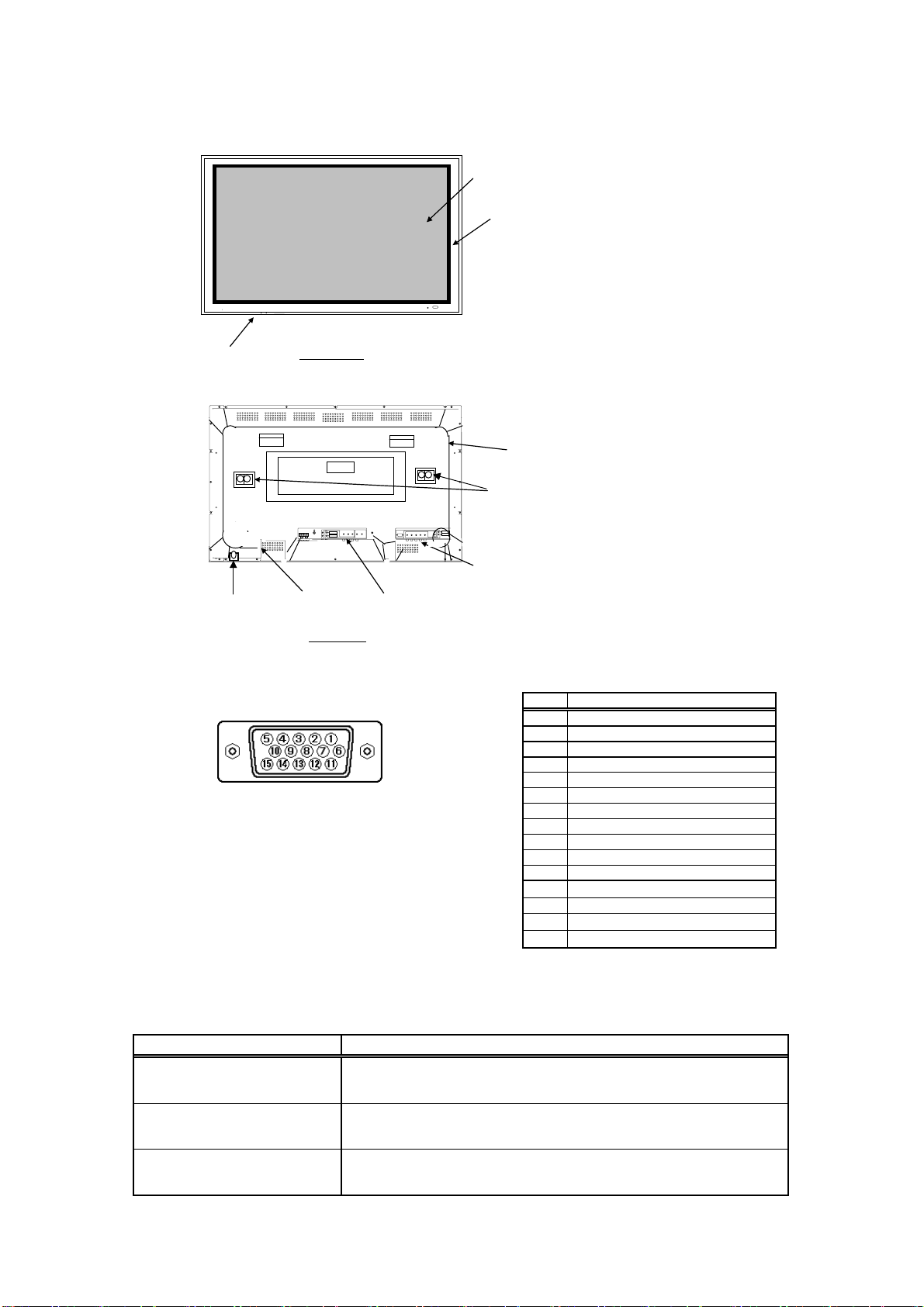
4. Names of each part
( )
Outlook
HITACHI
HITACHI
HITACHIHITACHI
S U B - P O W E R S E L E C T M E N U R G B /
V O L U M E
V I D E O
Filter
Panel
Front
Frame
Control
Switches
FRONT VIEW
Speaker
Terminals
AC Switch
A U D I O I N
S P E A K E R
T E R M I N A L
( 8 Ω 8 W )
L / M O N O
R
- - + +
R L
AC Inlet
REAR VIEW
P H 0 7 6 9 1
V I D E O 2
V I D E O 1
N e a r e r t e r m i n a l
C O M P O S I T E I N
C O M P O N E N T I N
手 前 側 端 子
F u r t h e r t e r m i n a l
S P / C P / C B B R R V I D E O Y
奥 側 端 子
Video Input Terminals
A U D I O I N
R G B 1
L / M O N O
D - S U B I N
R G B 2
R
R G B H V
RGB Input Terminals
Input terminal(D-sub connector)
Rear
Cover
PinNo Signal
1 Red Video, ( PR/CR )
2 Green Video (Sync. optional), (Y)
3 Blue Video (PB/CB)
4 No connection
5 No connection
6 Red Ground ( PR / CR Ground)
7 Green Ground ( Y Ground)
8 Blue Ground ( PB / CB Ground)
9 No connection
10 Ground
11 No connection
12
[SDA]
13 H.Sync. or H/V composite
14
V.Sync. [V.CLK]
15
[SCL]
:with RGB component input.
Message table
☛ Onscreen display
Indication Condition
The monitor indicates the
message
“NO SYNC SIGNAL”.
The monitor indicates the
message
“POWER SAVE”.
The monitor indicates the
message
“OUT OF FREQUENCY”.
The monitor detects no sync signal.
After a state whereby it does not sense a sync signal for 5 seconds
continued.
The monitor detects a sync signal which is out of specification, or
unstable.
4
Page 5
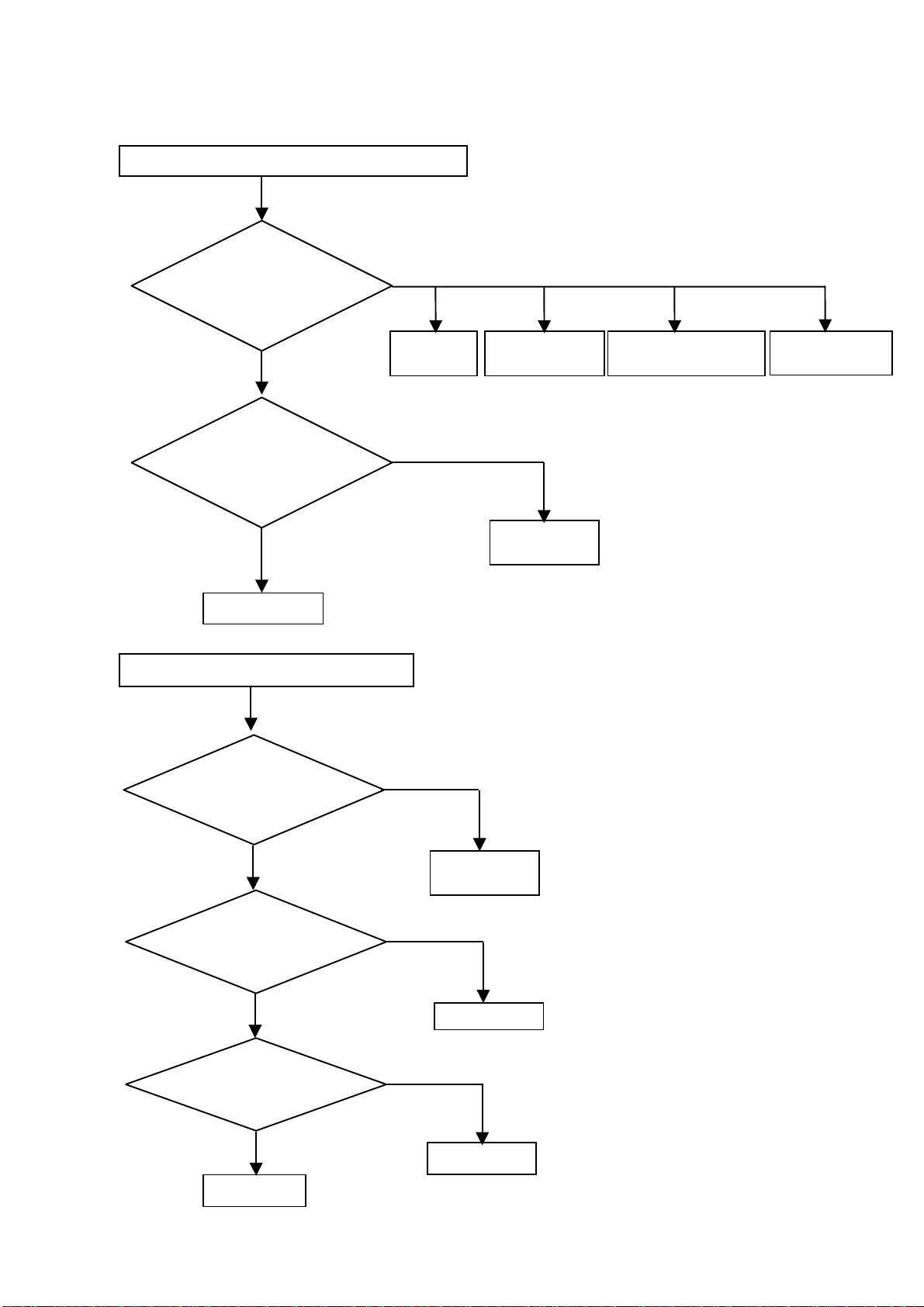
5. Trouble shooting
)
5.1 Trouble Shooting of Plasma Monitor
Power can not be turned on (LED is not light
Is the input voltage
applied to the AC/DC
Power unit ?
(CN61 ①, ③)
Yes
Are
Voltage
applied to pins ④⑦,⑪(PW01)
of the Signal PWB
④ +12V
Yes
Signal PWB
⑦ +6V
⑪ +4.5V
⑨ GND
No
AC inlet
No
Power switch
AC/DC
Power unit
AC Fuse
F901 T6.3AH 250V
FILTER PWB
Picture is displayed. But no sound
applied to pins ① (PVA)
of the Audio PWB
applied to
(PVA1)of the Audio PWB
there
Speaker Terminals
Are
Voltage
① +22~28V
Yes
Are Signal
Yes
④ GND
pin ⑤⑧ and ⑨⑪
Are
signals on
No
No
No
AC/DC
Power unit
Signal PWB
Yes
Speaker
Audio PWB
5555
Page 6
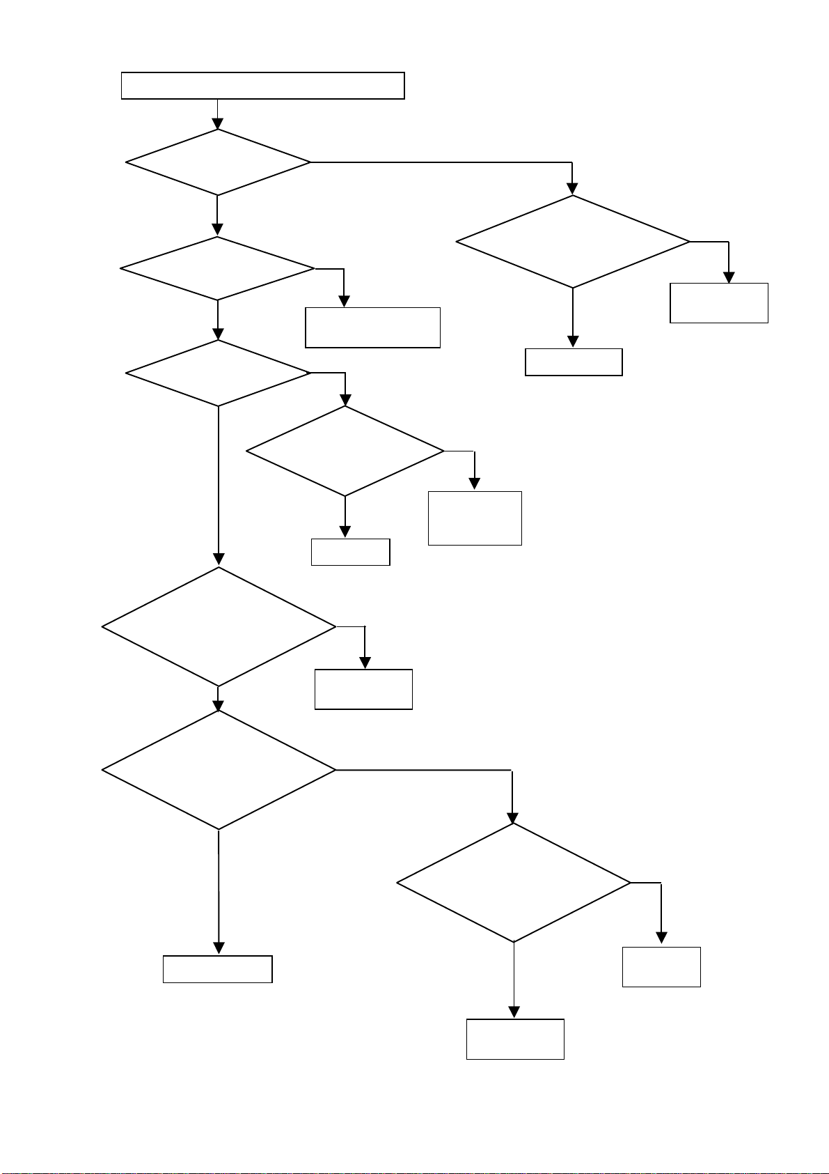
g)
Picture is not displayed (LED is lightin
Is the LED red or
green/orange
green/orange
Is it the power
saving mode?
No
Do the Fans
rotate?
Yes
CN304 and PFAN1
red
Yes
Input signal Cable
or Signal PWB
No
Is pin① of
7V more?
Yes
DC Fan
No
AC/DC Power
unit or Signal
PWB
Are
Voltage
applied to pins ⑦ (PW01)
of the Signal PWB
Yes
Signal PWB
⑦ +6V
⑨ GND
No
AC/DC
Power unit
Is Voltage
of the pin ⑥ (CN68)
on the AC/DC Power
unit 5V
Yes
Are Voltages
of the pin ①、⑩(CN64)
on the AC/DC Power
unit collect ?
Yes
① +50~70V
⑩ +75~90V
⑥ GND
Panel Module
No
AC/DC
Power unit
No
Is Voltage
of the pin ① (CN68)
on the AC/DC Power
unit collect ?
Yes
① +3V
③ GND
No
Panel
Module
AC/DC
Power unit
6666
Page 7
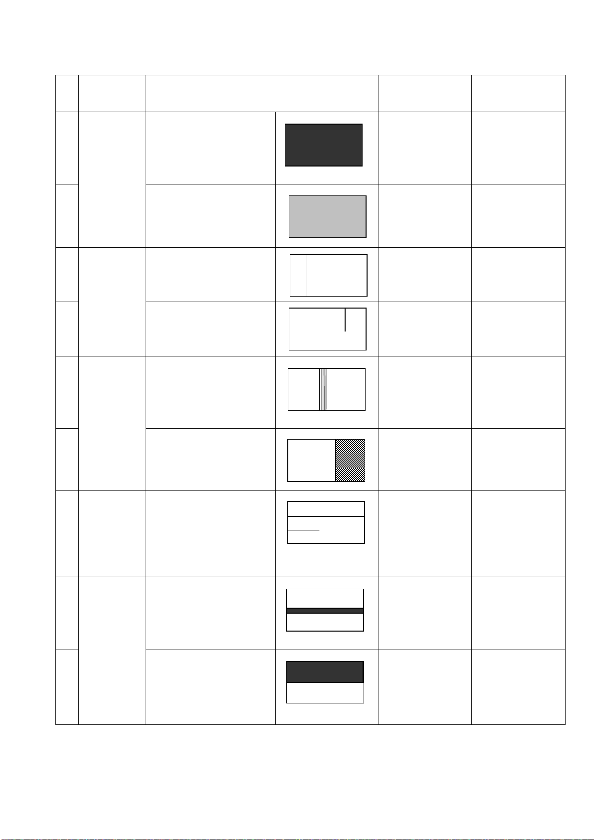
5.2 Trouble Shooting of Panel Module from the point view of Fault Symptom
NO
1
Entire
screen does
not light.
Fault
contents
After momentarily going
on, the screen becomes
black immediately or after
a few seconds. (Main
power is turned off.)
Fault status Suspected fault
location
X-SUS
Y-SUS
Panel chassis
LOGIC
ABUSL
ABUSR
Analysis
procedure
and measure
2
Vertical line
3 Single vertical line (of
4
5
Vertical bar
6
7 Horizontal
line
8 Horizontal
bar
9
Screen lights dimly even
on the back screen.
different color)
Vertical line from the
middle of effective scan
area (Vertical line of
different color)
Bar width of 1/7 of
horizontal size or in
multiples of 1/7, is
displayed. Abnormal
display.
Bar width of 3/7 or 4/7 of
the screen width, is
displayed. Abnormal
display. (Vertical line of
different color)
Single horizontal line (No
light) Or single horizontal
line does not light among
the effective scanning
area.
Single horizontal line
does not light.
Bar width of 1/8 or
multiples of 1/8 of the
screen height, is
displayed.
Abnormal (Screen does
not light)
Bar width of 1/2 of the
screen height.
Abnormal display
(Screen does not light)
LOGIC
Panel chassis
LOGIC
Panel chassis
Panel chassis
ABUSL
ABUSR
LOGIC
Above boards are
connected
ABUSL
ABUSR
LOGIC
Above boards are
connected
Panel chassis
Panel chassis
Panel chassis
Y-SUS
X-SUS
Above boards are
connected.
.
.
Replace LOGIC
board
Replace panel
chassis
Replace panel
chassis
Replace panel
chassis
7
Page 8
contents
sticking
Fault
Fixed display contents
are always displayed.
having abnormal
luminance are scattered
in the upper or lower part
of screen.
NO
10 Image
11 Stains Oval-shaped points
Fault status Suspected
fault
location
ABCDE
Panel
chassis
Panel
chassis
5.3 Trouble Shooting of Panel Module by using a Personal Computer
5.3.1 Setting up computer
Install the
panelinf.exe file
provided by DMD to the hard-disk of your PC.
Analysis procedure
and measure
Perform all white heat
run. After judgment,
replace panel chassis
Perform all white heat
run. After judgment,
replace panel chassis
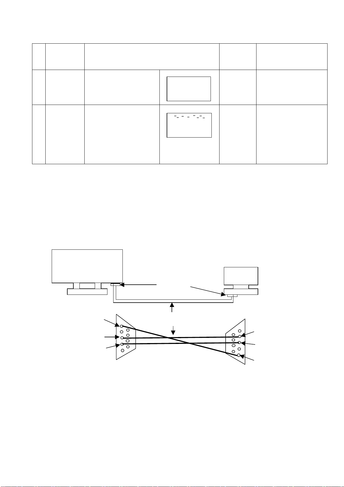
5.3.2 Connecting a computer
Plasma Monitor
PC
RS232C
Connector
⑤
③
RS232C
Cable
②
③
②
D-sub 9P
(female)
D-sub 9P
(female)
⑤
(1) Connect the RS-232C terminal of the computer to the RS-232C terminal of the plasma monitor, using
RS232C cable as above.
(2) Turn on the main power of the computer.
(3) Turn on the main power of the plasma monitor
.
8
Page 9

(4) For computer running WINDOWS:
Select
For computer running DOS/V:
(5) The following screen appears.
panelinf.exe
C : ¥ >panelinf
01:::: COND [Hex] xx
** 02:::: ERRC(CURRENT) [Hex] xx
03:::: ERRC(BEFORE1) [Hex] xx
04:::: ERRC(BEFORE2) [Hex] xx
05:::: ERRC(BEFORE3) [Hex] xx
06:::: ERRC(BEFORE4) [Hex] xx
07:::: ERRC(BEFORE5) [Hex] xx
08:::: ERRC(BEFORE6) [Hex] xx
09:::: ERRC(BEFORE7) [Hex] xx
10:::: ERRC(BEFORE8) [Hex] xx
11:::: ERRC(BEFORE9) [Hex] xx
12:::: ERRC(BEFORE10) [Hex] xx
13:::: ERRC(BEFORE11) [Hex] xx
14:::: ERRC(BEFORE12) [Hex] xx
15:::: ERRC(BEFORE13) [Hex] xx
16:::: ERRC(BEFORE14) [Hex] xx
17:::: ERRC(BEFORE15) [Hex] xx
18:::: OPERATION HOURS [Dec] xx
EXIT
from Explorer or My Computer →
<Enter>
→
PANEL DATA READ
*1 : Use COM1: the computer's communication port.
*2 : Set the communication setup as follows.
Speed : 9600 bps
Data : 7 bits
Parity : none
Stop bit : 1 bit
*3 : If the program starts up while the monitor power is not yet on, the menu
screen will not be displayed. At that time, turn on the monitor power, then the program
start up again.
5.3.3 Problem Analysis Procedure
(1) Check the error code (ERRC xx : hexadecimal number) from the CURRENT, (and BEFORE**)
error code read-out menu and detect the faulty position from the following table.
ERRC 00 is not valid.
<Enter>
<
Double Crick>
or
.
(2) Using the ↑ key or ↓ key, move the ** mark to EXIT and press <ENTER> key then
the screen returns to the WINDOWS or DOS screen.
9
Page 10
Error code table (H1 panel)
ERR
Code
Detect
position
(board)
04 LOGIC 3.3V power voltage has dropped LOGIC PSU
06 3.3V power startup is faulty X-SUS Y-SUS ADM1 - 8 PSU ABUS-L ABUS-R LOGIC
18 Internal I2C_SCL1_LOW level LOGIC
19 Internal I2C_ACK does not respond LOGIC
1C EEPROM initial setting is defective LOGIC
1D EEPROM write-down is defective LOGIC
1E EEPROM user initial setting is defective LOGIC
1F EEPROM factory setting reading is defective LOGIC
24 X-SUS Vex power voltage has decreased X-SUS LOGIC
25 Vex power voltage is excessive X-SUS
26 Vex power startup is faulty. X-SUS LOGIC
28 Vx power voltage has dropped X-SUS LOGIC
29 Vx power voltage is excessive X-SUS
2A Vx power startup is faulty. X-SUS LOGIC
2C Vpx voltage has dropped X-SUS LOGIC
2D Vpx voltage is excessive X-SUS LOGIC
30 Vpx1 voltage has dropped X-SUS LOGIC
31 Vpx1 voltage is excessive X-SUS LOGIC
34 Vpx2 voltage has dropped X-SUS LOGIC
35 Vpx2 voltage is excessive X-SUS LOGIC
39 Vs power current is excessive (during operation) X-SUS Panel LOGIC
3B Vs power current is excessive (during startup) X-SUS Panel LOGIC
44 Y-SUS Vey power voltage has dropped Y-SUS LOGIC
45 Vey power voltage is excessive Y-SUS
46 Vey power startup is faulty. Y-SUS LOGIC
4C Vpy voltage has dropped Y-SUS LOGIC
4D Vpy voltage is excessive Y-SUS LOGIC
50 Vpy1 voltage has dropped Y-SUS LOGIC
51 Vpy1 voltage is excessive Y-SUS LOGIC
54 Vpy2 voltage has dropped Y-SUS LOGIC
55 Vpy2 voltage is excessive Y-SUS LOGIC
59 Vs power current is excessive (during operation) Y-SUS Panel LOGIC
5B Vs power current is excessive (during startup) Y-SUS Panel LOGIC
5D Vs power current is excessive (during operation) Y-SUS SDM Panel LOGIC
61 PSU Vs power voltage is excessive PSU LOGIC
62 Vs power startup is faulty. X-SUS Y-SUS PSU LOGIC
X-SUS
64 Vex and Vpy power voltage has dropped LOGIC X-SUS Y-SUS
Y-SUS
65 Vex and Vey power voltage is excessive X-SUS Y-SUS
66
68 X-SUS Vw power voltage has dropped Y-SUS X-SUS LOGIC
69 Vw power voltage is excessive X-SUS
6A Vw power startup is faulty. Y-SUS X-SUS LOGIC
X-SUS
6C Vpx and Vpy voltage has dropped LOGIC X-SUS Y-SUS
Y-SUS
6D
Vex and Vey power startup is faulty. LOGIC X-SUS Y-SUS
Vpx and Vpy voltage is excessive LOGIC X-SUS Y-SUS
Contents
Suspected faulty board
(In the order of higher probability of defect)
(1) (2) (3) (4) (5) (6) (7)
Remarks
10
Page 11
ERR
Code
Detect
position
( board)
81 PSU Va power voltage is excessive PSU LOGIC
82 Va power startup is faulty. ADM1 - 8 PSU LOGIC ABUS-L ABUS-R
99 Va power current is excessive (during operation) ADM1 - 8 ABUS-L ABUS-R PSU LOGIC
9B Va power current is excessive (during startup) ADM1 - 8 ABUS-L ABUS-R PSU LOGIC
Contents
(In the order of higher probability of defect)
(1) (2) (3) (4) (5) (6) (7)
Suspected faulty board
Remarks
9D Va power current is excessive
(during operation)
A5 ADM1 ADM1 has abnormal heat generation. ADM1 PSU LOGIC
A9 ADM2 ADM2 has abnormal heat generation. ADM2 PSU LOGIC
AD ADM3 ADM3 has abnormal heat generation. ADM3 PSU LOGIC
B1 ADM4 ADM4 has abnormal heat generation. ADM4 PSU LOGIC
B5 ADM5 ADM5 has abnormal heat generation. ADM5 PSU LOGIC
B9 ADM6 ADM6 has abnormal heat generation. ADM6 PSU LOGIC
BD ADM7 ADM7 has abnormal heat generation. ADM7 PSU LOGIC
C5 ADM8 ADM8 has abnormal heat generation. ADM8 PSU LOGIC
E2 LOGIC 5V power startup is faulty. X-SUS Y-SUS PANEL PSU ABUS-L ABUS-R LOGIC
ADM1 - 8 ABUS-L ABUS-R PSU LOGIC Excess current is
detected In
ACCC operation.
It can possibly
occur depending
on screen
display.
11
Page 12

Error code table (H2 panel)
ERR
Code
Estimate
Detect
position
Detection position The states in error
Contents Remarks
generation
(board)
02 Wavy pattern ROM In startup Wavy pattern ROM data errors
04 The ordinary time 3.3V power voltage has dropped
06
18 Internal I2C_SCL1_LOW level (SCL1 error)
19
1C Initialization non-execution EEPROM initial setting is defective
1D Verify error EEPROM write-down is defective
1E User sum error EEPROM user initial setting is defective
1F
24 Vex power voltage has dropped
25
26
28 Vx power voltage has dropped
29
2A
2C Vpx 1,2 power voltage has dropped
2D
30 Vpx1 power voltage has dropped
31
34 Vpx2 power voltage has dropped
35
39 The ordinary time Isx power current is excessive
3B
44 Vey power voltage has dropped
45
46
4C Vpy1,2 power voltage has dropped
4D
50 Vpy1 power voltage has dropped
51
54 Vpy2 power voltage has dropped
55
59 The ordinary time Isy power current is excessive
5B
5D
61 The ordinary time Vs power voltage is excessive
62
64 Ve power voltage has dropped
65
66
68 Vw power voltage has dropped
69
6A
6C Vp power voltage has dropped
6D Vp power voltage is excessive
81
82
99 The ordinary time Ia power current is excessive
9B
9D
A5 ADM1 ADM1 has abnormal heat generation.(shutdowns)
A9 ADM2 ADM2 has abnormal heat generation.(shutdowns)
AD ADM3 ADM3 has abnormal heat generation.(shutdowns)
B1 ADM4 ADM4 has abnormal heat generation.(shutdowns)
B5 ADM5 ADM5 has abnormal heat generation.(shutdowns)
B9 ADM6 ADM6 has abnormal heat generation.(shutdowns)
BD
C5 The ordinary time ADM8 has abnormal heat generation.(shutdowns)
E2
LOGIC
3.3V
Internal I2C -
EEPROM
X-SUS
Y-SUS
X-SUS
Y-SUS
ADM
ADM ADM8
Vex
Vx
Vpx The ordinary time
Vpx1 The ordinary time
Vpx2 The ordinary time
Isx
Vey
Vpy The ordinary time
Vpy1 The ordinary time
Vpy2 The ordinary time
Isy
Isp The ordinary time SDM power current is excessive
Vs
Ve
Vw
Vp
Ia
ACCC The ordinary time IaACCC power current is excessive
ADM7
In startup Without starting with 3.3 V voltage.
Internal I2C_ACK does not respond (SDA1 error)
Factory sum error EEPROM factory setting reading is defective
The ordinary time
Vex power voltage is excessive
In startup Vex power startup is faulty.
The ordinary time
Vx power voltage is excessive
In startup Vx power startup is faulty.
Vpx 1,2 power voltage is excessive
Vpx1 power voltage is excessive
Vpx2 power voltage is excessive
In startup Isx power current is excessive (in startup)
The ordinary time
Vey power voltage is excessive
In startup Vey power startup is faulty.
Vpy1,2 power voltage is excessive
Vpy1 power voltage is excessive
Vpy2 power voltage is excessive
In start Isy power current is excessive (in startup)
In startup Vs power startup is faulty.
The ordinary time
Ve power voltage is excessive
In start Ve power startup is faulty.
The ordinary time
Vw power voltage is excessive
In startup Vw power startup is faulty.
The ordinary time
Va power voltage is excessive
In startup Va power startup is faulty.
In startup Ia power current is excessive (during startup)
The ordinary time
ADM7 has abnormal heat generation.(shutdowns)
In startup Vcc power startup is faulty.
12
Page 13

5.4 Checking serial ID number of Panel Module (14 digits
The serial ID number of the panel module that is brought in for service and that of the completed panel
chassis has the structure as shown below.
)
The serial ID number is shown on the bar code label that is attached to the rear of the chassis (aluminum).
P7A
51---H1 panel, 71,75---H2 panel
A-Z (excluding I and O)
Lot No.: 001-999
A-Z (excluding I and O)
1-3
Production week code: 01-53
Production year (low digit): 0-9
Product code: P7A model 42 type
Model
Panel
Module
H1 panel
Module
H2 panel
Module
2 36 131D2 01 - 51
CMP4121HDU-
512/512S/
512SH/512SA
○ ○
Version No.: 01-99
CMP
4121HDE-
302/303S
CMP
4201U/J
○ ○ ○
42PMA
400E/A/B
CMP
4202U/E
CMP
4203W
○
13
Page 14

14
to
to
toto
chassis
chassis
chassischassis
VIDEO 1
VIDEO 1
VIDEO 1VIDEO 1
OUT
OUTPUT
PUT
OUTOUT
PUTPUT
VIDEO 1
VIDEO 1
VIDEO 1VIDEO 1
INPUT
INPUT
INPUTINPUT
(COMPOSITE)
(COMPOSITE)
(COMPOSITE)(COMPOSITE)
VIDEO 1
VIDEO 1
VIDEO 1VIDEO 1
INPUT
INPUT
INPUTINPUT
(S
(S----VIDEO)
VIDEO)
(S(S
VIDEO)VIDEO)
VIDEO 2
VIDEO 2
VIDEO 2VIDEO 2
INPUT
INPUT
INPUTINPUT
(COMPONENT)
(COMPONENT)
(COMPONENT)(COMPONENT)
VIDEO 1
VIDEO 1
VIDEO 1VIDEO 1
AUDIO
AUDIO
AUDIOAUDIO
INPUT
INPUT
INPUTINPUT
VIDEO 2
VIDEO 2
VIDEO 2VIDEO 2
AUDIO
AUDIO
AUDIOAUDIO
INPUT
INPUT
INPUTINPUT
L+
L+
L+L+
GND
GND
INLET
INLET
INLETINLET
GNDGND
GND
GND
GNDGND
EXT.
EXT.
EXT.EXT.
SPEAKER
SPEAKER
SPEAKERSPEAKER
terminal
terminal
terminalterminal
AC
AC
ACAC
AC100V~240V
SIGNAL FLOW
6. BLOCK DIAGRAM (CMP4121HDE/CMP4202E/42PMA400E)
RGB 1
RGB 1
RGB 1RGB 1
AUDIO
AUDIO
AUDIOAUDIO
INPUT
INPUT
INPUTINPUT
JOINT
VIDEO
VIDEO
VIDEOVIDEO
PPPPV1
V1
V1V1
A+5V
AUDIO L,R
AUDIO L,R
AUDIO L,RAUDIO L,R
AUDIO L,R
AUDIO L,R
AUDIO L,RAUDIO L,R
SP L
SP L
SP LSP L
PAS3
PAS3
PAS3PAS3
SP R
SP R
SP RSP R
R+
R+
+
+
PF1
PF1
PF1PF1
PAS4
PAS4
PAS4PAS4
FILTER
FILTER
FILTERFILTER
POWER SW
POWER SW
POWER SWPOWER SW
PAS1
PAS1
PAS1PAS1
PFA
PFA
PFAPFA
CN61
CN61
CN61 CN 61
AUDIO
AUDIO
AUDIOAUDIO
JOINT
JOINTJOINT
+9V +12V
STB +5V
PVA
PVA
PVAPVA
CN
CN10
102222
CNCN
1010
AC100V~240V
CN30
CN30
CN30CN30
+12V
MMMMFN
FN2222
FNFN
(FAN2)
(FAN2)
(FAN2) (FAN2)
+4.5V
+5.6V
STB +5V
PA
PAV1
PAPA
+25V
POWER
POWER (AC
(AC----DC)
POWERPOWER
(AC(AC
FAN
CONNECTOR
V1
V1V1
PPPPVA
VA
VAVA
DC)
DC)DC)
CN66
CN66
CN66CN66
PPPP002
002
232C)
232C)23 2C)
RGB 2
RGB 2
RGB 2RGB 2
INPUT
INPUT
INPUTINPUT
RGB 1
RGB 1
RGB 1RGB 1
INPUT
INPUT
INPUTINPUT
CN64
CN64
CN64CN64
002002
PW0
PW0
PW0PW0
PA
PA01
PAPA
PPPPSE
SE
SESE
(RS
(RS232C)
(RS(RS
PS
PSF P001
F P001
PSPS
F P001F P001
01
0101
STAND
STAND----BY
STANDSTAND
REG.
REG. 4.5V,
REG.REG.
3.3V
REG.
REG. 25V
REG.REG.
12V
10~12V
5V(Vcc)
REG.
REG. 60V(Va)
REG.REG.
82V(Vs)
SIGNAL
SIGNAL
SIGNALSIGNAL
RGB 2
RGB 2----IN(
RGB 2RG B 2
RGB
RGB
RGB RGB
BY. 5. 6V
BYBY
CN68
CN68
CN68 CN68
RS232C
IN(DDDD----Sub15P
IN(IN(
Sub15P))))
Sub15PSub15P
CN65
RGB 2
RGB 2
RGB 2RGB 2
AUDIO
AUDIO
AUDIOAUDIO
INPUT
INPUT
INPUTINPUT
+4.5V
+5.6V
+12V
PPPPW01
W01
W01W01
CN101
CN101
CN101CN101
CN65 CN67
CN65 CN65
CN67
CN67 CN67
MFN1
MFN1
MFN1MFN1
+12V
+12V
+12V+12V
(FAN1)
(FAN1)
(FAN1)(FAN1)
PFAN1
PFAN1
PFAN1PFAN1
Pk01
Pk01 PSC1
Pk01 Pk01
PPPPL01
L01
L01L01
YYYY----SUS
PP01
PP01
PP01PP01
CN69
CN69
CN69CN69
ADDRESS
ADDRESS BUS L
ADDRESS ADDRESS
CN52
CN52
CN52CN52
TACT SW
TACT SW
TACT SWTACT SW
STB +5V
PSC1
PSC1PSC1
SUS
SUSSUS
BUS L
BUS L BUS L
CN33
CN33
CN33CN33
PSC2
PSC2
PSC2PSC2
CN32
CN32 CN22
CN32CN32
CN7
CN7
CN7CN7
VOLTAGE SUPPLY FLOW
CONNECTOR
CIRCUIT BOARD
LED
LED/RECEIVER
LEDLED
STB +5V
PANEL MODULE
PANEL MODULE
PANEL MODULEPANEL MODULE
(REAR VIEW)
CN1
CN1
CN1CN1
LOGIC
LOGIC
LOGICLOGIC
CN6
CN6
CN6CN6
SIGNAL FLOW
SIGNAL FLOW SIGNAL FLOW
VOLTAGE SUPPLY FLOW
VOLTAGE SUPPLY FLOW VOLTAGE SUPPLY FLOW
CONNECTOR
CONNECTOR CONNECTOR
CIRCUIT BOARD
CIRCUIT BOARD CIRCUIT BOARD
/RECEIVER
/RECEIVER/RECEIVER
CN22
CN22CN22
ADDRESS BUS R
ADDRESS BUS R
ADDRESS BUS RADDRESS BUS R
XXXX----SUS
CN23
CN23
CN23CN23
SUS
SUSSUS
CN42
CN42
CN42CN42
Page 15

7. Disassembly diagram
(1) Remove Back Cover
Lay down the Plasma display so that
the face is down on the soft thick (over
50mm) cushion.
Be careful not to be damaged the face
of Front Filter.
Remove 28screws(a) then remove
Back Cover.
At this time be careful not to be
damaged edges of Back Cover and its
coated face.
(2) Remove Filter PWB
Remove 2screws(b) and remove
"Insulation Cover".
Remove 2screws(c) of earth wires.
Disconnect PFA(EV-6P) and
PF1(EV-3P) connectors.
Remove 2screws(d) of AC Power
Switch Folder and remove 4screws(e)
and remove Filter P.W.B.
Remove 2 screws(f) and remove AC
Power Switch.
(3) Remove Signal PWB with PWB MTL,
;Signal PWB
Disconnect PP01(LVDS),
PW01(EH-13P), P001(FHR-50),
PA01(PH-13P),
PL01(PH-6P),PK01(PH-5P),PW02(
PH-7P),PFAN1(PH-3P)and
P002(PH-12P) connectors.
Be careful not to be damaged the PP01
and P001 connector holders.
Remove 4screws(i) then remove Signal
P.W.B with SIG PWB MTL.
(4)-1 Video Unit/JOINT PWB and
Audio PWB with PWB MTL.
;JOINT PWB
Disconnect PAV(PH-7P), PSE(PH-12P),
and PSF(FHR-50) connectors.
;
Audio PWB
Disconnect PVA, PAS1, and PAV1
connectors.
Remove 6 screws(k) then remove
VIDEO PWB MTL.
(4)-2 VIDEO Unit
Remove 2screws(j) then pull out Video
Unit.
Screw(e)
Screw(c)
Screw(d)
AC Power SW
Screw(k)
Audio P.W.B
Screw(j)
Screw(a)
Screw(b)
JOINT P.W.B.
VIDEO Unit
××××
28
Insulation Cover
Screw(f)
SIGNAL P.W.B
Screw(c)
Filter PWB
Screw(i)
.
15
Page 16

(5) Remove Front Frame
(
(
Remove 18screws(m) then remove
Front Frame.
Be careful not to fall down the Front
Frame when remove 18screws(m).
(6) Remove Front Filter (Glass)
Remove 8screws(n), and remove Filter
Fix Metal then remove Front Filter.
When attach the new Front Filter to the
Front Frame, locating the conducting
electrode side to the inside, and attach
Filter Fix Metal.
(7) Remove Fan (MFN1)
Remove 1screw(o) and disconnect
PFAN1(PH-3P) connector,
then remove Fan. (only H1 panel)
(8) Remove Main Frame
Lay down the Plasma Display so that
the face is down on the soft thick (over
50mm) cushion. Be careful not to be
damaged the face of Display Panel.
Disconnect CN61(EV-6P) connector.
(H1 panel)
Remove 8 screws(q) and 5screws(r)
then disconnect CN1(LVDS) connector
which is attached Panel Module's Logic
Board. Remove Main Frame.
(H2 panel)
Remove 8 screws(q) then disconnect
CN1(LVDS) connector which is
attached Panel Module's Logic Board.
Remove Main Frame.
Screw(m)×18
Screw(n)×8
Screw(r)
Filter Fix Metal
Front Filter
Screw(q)×8
Screw(r)
Screw(o)
Screw(q)
Screw(q)
Screw(r)
Screw(r)
H1 panel)
Screw(q)×8
Screw(r)
H2 panel)
16
Page 17

(9) Remove Power Unit P.W.B.
(y)
)
Disconnect CN101(EH-13P),
CN102(EH-6P)CN64(VH-10P),
CN65(VH-9P),CN66(PH-7P),
CN67(PH-7),CN68(PH-6P) and CN69
( FLAT Cable).
Be careful not to be damaged the
CN69 connector folder. Remove 10
screws(v) then remove Power Unit
P.W.B.
(10) Remove Fan (H1/H2 panel)
Disconnect CN304 connector.
Remove 2screws(p) then remove Fan
fix metal.
(11) Remove Panel LOGIC P.W.B.
Disconnect CN1, CN2, CN3, CN4, CN5,
CN6 and CN7 connectors. Be careful
not to be damaged the CN2, CN3, CN4,
CN5 and CN7 connector folders.
Remove 4screws(w) then remove
Panel LOGIC P.W.B.
(12) Remove Panel X-SUS P.W.B.
Disconnect CN21, CN22 and CN23
connectors. Be careful not to be
damaged the CN21 connector folder.
Remove 9screws(x) then remove Panel
X-SUS P.W.B. pulling out from CN24
and CN25 connectors.
(13) Remove Panel Y-SUS P.W.B.
Disconnect CN31, CN32 and CN33
connectors. Be careful not to be
damaged the CN31 connector folder.
CN34 and CN35 connector Remove 9
screws(y) then remove Panel Y-SUS
P.W.B. pulling out from CN34 and
CN35 connectors
Screw
×9
Screw(v)×10
Y SUS
ABUS L
Screw(z1)×11 Screw(z2)×11
Screw(p)×2
Power Unit
LOGIC
Screw(w)×4
ABUS R
Screw(x
X SUS
×9
(14) Remove Panel ABUS R P.W.B
Disconnect CN41, CN42, CN43, CN44, CN45 and CN46
Connectors. Be careful not to be damaged the CN41,
CN43, CN44, CN45 and CN46 connectors folders.
Remove 11 screws (z2), then remove Panel ABUS R P.W.B.
(15) Remove Panel ABUS L P.W.B
Disconnect CN51, CN52, CN53, CN54, CN55 and
CN56 connectors. Be careful not to be damaged
the CN51, CN53, CN54, CN55 and CN56 connector folders.
Remove 11 screws (z1), then remove Panel ABUS L P.W.B.
17
Page 18

8. Re-Adjustment
After
changing the Panel Module, re-adjustment is needed according to the item 8.1.to 8.5.
For Power Unit, item 8.1; for Signal Board, item 8.2 to 8.5* and for Video Board, item 8.2,
8.4,8.5 are needed.
It is recommended to start re-adjustment after 30 minutes warm-up with the Burn-in signal.
*) When it is not inserted into VIDEO Unit of optional Board in Signal Board replacement,
VIDEO Unit becomes necessary. In this case, insert the dummies' VIDEO unit and execute the above
adjustment item.
How to set to Burn-in signal
(red, green, blue, white, yellow, cyan, magenta, black signal)
Turn off the sub power button (or power button on the Remote Controller), then turn on the
SUB POWER button for more than 5 seconds while you keep pushing VOLUME▼ and
RECALL buttons located on the bottom of the set.
When you fall out from Burn-in mode, turn off the sub power button (or power button on the
Remote Controller),then turn on the SUB POWER button for more than 5 seconds while you
Keep pushing VOLUME▼ button located on the bottom of the set.
8.1 Vs and Va voltage adjustment on Power Unit
How to prepare
1.Connect the DC Voltmeter to the Vs test point and
the GND point (or the Va test point and the GND point)
on the Power Unit.
2.Connect VGA (75), no-setup, and all black signal to
RGB input terminal.
3.Check the amount of Vs and Va voltages printed on the
label located lower left side on the Panel Module.
How to adjust
1.If the difference of the printed voltage of Vs and the
value of DC Voltmeter of Vs is over ±0. 4 V, adjust
the Vs ADJ Volume located upward on the Power Unit
to within ±0. 4 V.
2. If the difference of the printed voltage of Va and the
value of DC Voltmeter of Va is over ±0. 4 V, adjust
the Va ADJ Volume located upward on the Power Unit to within ±0. 4 V.
Label
Power Unit
Y-sus
VR51Vs ADJ.(IC591)
PIN301 Va
VR51 Va ADJ.(IC391)
Power
Unit
Panel Module
Rear View
PIN502 GND
PIN501 Vs
X-sus
18
Page 19

8.2 Personal Computer (PC) input and Video input Automatic amplitude adjustment
How to set to service adjustment mode
Turn off the sub power button (or power button on the
Then turn on the SUB POWER button for more than 5 seconds while you keep pushing
INPUT SELECT and RECALL buttons located on the bottom of the set.
Preparation
1. Indicate service adjustment mode.
2. Select SHIP.2, then press [RECALL] button more than 3 seconds by
(The screen disappears, and EEPROM is initialized.)
A service adjustment mode screen appears after initialization end again.
* : Select items : Press [ ▲▲▲▲, ▼▼▼▼ ] botton of Remote Controller.
Adjust Data : Press [
Memorize the data : Press [ ENTER] botton of Remote controller.
Adjustment Signal
How to adjust (VIDEO input)
1.Input 525p(480p) adjustment signal into VIDEO2 input terminal.
2.Change CONTRAST of the MENU screen from DYNAMIC to LINEAR.
3.Service adjustment mode screen again
4.Select No.259. (RGB ADJ.)
5.Press [ENTER] button more than 2 seconds. * Start the automatic adjustment.
6.Complete the adjustment after disappear ADJUSTMENT indication.
7.Change CONTRAST of the MENU screen from LINER to DYNAMIC again.
How to adjust (PC input)
1.Input VGA (60Hz) adjustment signal into RGB input terminal.
2.Indicate service adjustment mode.
3.Select No.259. (RGB ADJ.)
4.Press [ENTER] button more than 2 seconds. * Start the automatic adjustment.
5.Complete the adjustment after disappear ADJUSTMENT indication.
*Never adjust without use our specify signal.
If press [ENTER]button at No.259 by mistake, the picture becomes abnormal (Black level,
Contrast and Color.)
0.7V
*Fig.1 Adjustment Signal
Black White
,
] botton of Remote controller.
Black pattern : Set pedestal level.
This signal must not insert character.
Remote Controller
),
Remote Controller.
19
Page 20

8.3 Color temperature adjustment for PC
How to prepare
Set signal generator output signal to Full White.
1.
2.Signal condition
VGA (75): 0.7Vp-p, Set up level: 0V
3.Input the signal into RGB (D-sub) terminal.
4.Set Picture setting up to reference.
How to adjust
1.Indicate service adjustment mode and adjust as follows by Remote Controller.
2.Measurement probe of CRT Color Analyzer CA-100 is set on the center of screen.
3.Adjust color temperature as follows by reducing one or two numbers of No.9, 10, 11.
(
At least one of these datas should be 255.)
PC color temperature (COOL)
x=0.285±±±±0.005, y=0.294±±±±0.005, at 9300 K
4. Adjust color temperature as follows by reducing one or two numbers of No.12, 13, 14.
(At least one of these datas should be 255.)
PC color temperature (NORMAL)
x=0.300±±±±0.005, y=0.298±±±±0.005, at 7600 K
5.Adjust color temperature as follows by reducing one or two numbers of No.15, 16, 17.
(At least one of these datas should be 255.)
PC color temperature (WARM)
x=0.314±±±±0.005, y=0.327±±±±0.005, at 6500 K
Suggestion
1.Luminance of panel surface is less than 20 lux to arrange adjustment environment.
2.Adjstment is reduce value adjustment only. (Impossible to increase value adjustment.)
3.Color select mode is automatically set to COOL while adjustment No.9, 10 and 11.
4.Color select mode is automatically set to NORMAL while adjustment No.12, 13 and 14.
5.Color select mode is automatically set to WARM while adjustment No.15, 16 and 17.
8.4 Color temperature adjustment for Video
How to prepare
Set signal generator output signal to Full White.
1.
2.Signal condition
3.Input the signal into VIDEO2 terminal.
4.Set Picture setting up to reference.
5.Make sure that CONTRAST is LINEAR.
6.Do after color temperature adjustment of PC.
480i/60Hz Component signal
Video level: 0.714Vp-p,
Sync level: 0.286Vp-p
Set up level: 0V
20
Page 21

How to adjust
1.Indicate service adjustment mode and adjust as follows by Remote Controller.
2.Measurement probe of CRT Color Analyzer CA-100 is set on the center of screen.
3.Adjust color temperature as follows by reducing one or two numbers of No.0, 1, 2.
(At least one of these datas should be 255.)
VIDEO color temperature (COOL)
x=0.285±±±±0.005, y=0.294±±±±0.005, at 9300 K
4. Adjust color temperature as follows by reducing one or two numbers of No.3, 4, 5.
(At least one of these datas should be 255.)
VIDEO color temperature (NORMAL)
x=0.300±±±±0.005, y=0.298±±±±0.005, at 7600 K
5.Adjust color temperature as follows by reducing one or two numbers of No.6, 7, 8.
(At least one of these datas should be 255.)
VIDEO color temperature (WARM)
x=0.314±±±±0.005, y=0.327±±±±0.005, at 6500 K
Suggestion
1.Luminance of panel surface is less than 20 lux to arrange adjustment environment.
2.Adjstment is reduce value adjustment only. (Impossible to increase value adjustment.)
3.Color select mode is automatically set to COOL while adjustment No.0, 1 and 2.
4.Color select mode is automatically set to NORMAL while adjustment No.3, 4 and 5.
5.Color select mode is automatically set to WARM while adjustment No.6, 7 and 8.
8.5 Reset adjustment
Always set to factory Setting mode, to prevent error picture, Reset should be done.
When above adjustment is finished, turn off the SUB POWER button (or power button on
the
Remote Controller
How to set to factory Setting
Receive a signal in RGB1.
Turn off the SUB POWER button (or power button on the
Then turn on the sub power button for more than 5 seconds while you keep pushing
SIZE and RECALL buttons located on the bottom of the set.
You fall out from factory Setting mode, turn off the SUB POWER button (or power button on
the Remote Controller).
) and Main power Switch.
Remote Controller
),
21
Page 22

9 Wiring Drawing
9.1 Panel Module and Power Unit section
POWER UNIT
PANEL YSUS
CN33
EJ203
CN32
CN22-CN32間コネクタ布線注意:
電源基板1次側に接触しない様スタイルどりし、
(CN22)側に出来るだけ手繰りよせ布線のこと。
ESP
EAP
TO AUDIO P.W.B
(PVA)
CN69
(*1) (*1) (*1)
CN7
ECN7
(*8)
TO SIGNAL P.W.B
(PW01)
CN102
CN68
(*1)
EJ206
PANEL LOGIC
CN65
CN67
CN101
CN66
CN6
CN1
CN64
(*7)
EJ202
CN22
CN23
ECN1
TO SIGNAL P.W.B
(PP01)
NCN11
Ferrite Core
フェライト・コア(中型)
(*2)(*3)
PANEL XSUS
PANEL L-ADR
CN52
EJ205
EJ204
The lead must run onto the fram e of a chassis.
MAIN FRAME(#402)取付時
ケーブルをはさみ込まないよう注意のこと。
CN42
PANEL R-ADR
22
Page 23

(φ8)
9.2 Plasma Monitor((((H1/H2 panel))))
SP端子は、CLOSE
状態にすること。
SP TERM.R
P.W.B
ESC2
For H2 panel
FLOW
MFN2
POWER UNIT
Roll 3 times
3回巻くこと.
CN304
N020
パースロック(φ8.0)
Pathlook
MF2
CN64
CN65
FLOW
MFN1
For H1 panel
EFP
パースロック(φ15)
)(
EAP
From Power Unit
(CN102)
PVA
PAV1
Z007
EVA
N21
パースロック(φ15)
Pathlook(φ15)
(*1)
AUDIO
P.W.B
VIDEO P.W.B
The lead must not run onto
ヒートシンクに接触しないよう
EAS1
the frame of a chassis.
また、フレームとバックカバーとで
挟み込まないようスタイルどりのこと。
(*1)
PAS4
E1
(*1)
E906
ネジ止め
Safety Ground
(安全アース)
C903
ダイキャストフレームの
The lead must not run onto the
ボス部品に乗り上げないよう
frame of a chassis.
スタイルどりのこと。
(*1)
PFA
FILTER
P.W.B
E905
ネジ止め
(*1)
(E905)
PF1
(*1)
CN61
(*1)
(*1)
(*1)
Pathlook(φ15)
From Power Unit
(CN101)
H1 Panel
N019
ESP
余長リードは
ここで弛ませること。
(*1)(*1)
フェライト・コア
Ferrite
EVP1
PSE
(中型)(*2)
JOINT P.W.B
N017
パースロック(φ8)
Pathlook(φ8)
NVS21
フェライト・ コア
Ferrite Core
(中型)(*2)
Z005
(*1)
NCN11
PVA
(*4)
EVS1
PSF
EVS2
FLOW
MFN1
(*7)
(*1)
(*1)
(*1)
(*1)
EF1
NCN12
フェライト・コア(小型)
Ferrite Core
PP01
ECN1
P001
NVS2
P002
(*1)
PFAN1
(*2)
From Panel Logic(CN1)
Ferrite Core
(フラット)
(Flat)
フェライト・コア
(*4)
15±2
The position of FAN only differs.
SP端子は、CLOSE
(
状態にすること。
SP TERM.L
P.W.B
PAS3
(*1)
PW02 PW01
PA01
EVA
ESC2
SIGNAL P.W.B
(L=30mm)
テープにて EAS1 ケーブルを
アルミフレームに固定のこと。
PL01
Z006
TAPE
)
(*1)
(*1)
PK01
Z004
テープ貼り
TAP E
*電源スイッチの
半田付部に当たらない
ように弛みがないこと。
*テープが#451
The tape must not run onto the
(POW BOTTOM PANEL)
POWER BOTTOM HOLDER.
に乗り上げない様に付線注意のこと。
LED/RECEIVER P.W.B
PSC2
(*9)
POWER SWITCH
AC
INLET
N018
パースロック(φ8)
Pathlook(φ8)
ヒューズホルダに接触しないよう、又
Does not touch Fuse Holder.
C903 に乗り上げないようスタイルどりのこと。
PAS1
10±2
Z003
パーマセルテープ 幅19(L=70)で
TAPE TAPE
EAS1 ケーブルを固定のこと。
10±2
Z002
パーマセルテープ 幅19 (L=70)で
EAS1 ケーブルを固定のこと。
(*1)
ESC1
PSC1
Z001
パーマセルテープ 幅19(L=100)で
TAPE
EAS1 ケーブルを固定のこと。
23
(*1)
TACT SW P.W.
Page 24

THE UPDATED PARTS LIST
FOR THIS MODEL IS
AVAILABLE ON ESTA
Page 25

SM0064
Power Supply Block Diagram
HITACHI
Page 26

SM0064
Panel Connectors
HITACHI
Page 27

NO P OWE R
NO•P OWE R
NO V s ,Va,Vcc,S T B
OK
S T B
OK
NO PICTURE
& S OUND
F U S E
NG
under 130V
NO V s,V a,Vcc
S T B
NG
check voltage
D011(k ) -J13
Q103,R 005
NG
over 130V
D161,IC101,Q104,
Q108,etc
impedance check
D001
OK
impedance checkQ003/Q004
OK
impedance check
Q201
OK
impedance check
Q301
S ee NO P OWE R
NG
D001
NG
Q003/Q004,
etc
NG
Q201,IC201
D210,Q202,etc
NG
Q301,IC301
D301,Q303,etc
V a : n o u p r i s e
V s : d o w n a f t e r u p
I C 3 0 1 , Q 3 0 3 ,
P C 3 0 1 , P C 3 0 2
D 3 1 0 , I C 3 9 1 ,
etc
OK
V cc
NO PICTURE
i m p e d a n c e c h e c k
V s L I N E
OK
i m p e d a n c e c h e c k
V a L I N E
OK
S W O N
V s : n o u p r i s e
V a : d o w n a f t e r u p
I C 5 9 1 , Q 5 0 1 ,
I C 5 0 1 , D 5 3 2 ,
Q 5 3 0 , P C 5 0 1 ,
P C 5 0 2 , D 2 8 0 ,
D 2 8 1 , e t c
NGOK
NG
NG
C N 6 4 , C N 6 6CN67
check voltage
J58 - J13
u n d e r 3 0 0 V
over 300V
I C 0 0 1,D005•D008,
R L 0 0 1 , PC003,Q010,etc
N O V s , V a
o p e n c o n nector
i m p e d a n c e check
V a L I N E
OK OK
open connector
NG
P D P module Va
D 3 5 1 D551,D552
NG
IC201,Q202,P C201,
P C202,P C252,P C256,
D210,etc
CN64,CN65
impedance check
Vs L INE
NG
P D P module Vs
NG
SM0064
Power Supply Unit Troubleshooting
HITACHI
Page 28

SM0064
Power Supply Circuit Board
HITACHI
Page 29

SM0064
Power Circuit Schematic - 1 of 5
HITACHI
Page 30

SM0064
Power Circuit Schematic - 2 of 5
HITACHI
Page 31

SM0064
Power Circuit Schematic 3 0f 5
HITACHI
Page 32

SM0064
Power Circuit Schematic - 4 of 5
HITACHI
Page 33

SM0064
Power Circuit Schematic - 5 of 5
HITACHI
Page 34

Hitachi, Ltd. Tokyo, Japan
International Sales Division
THE HITACHI ATAGO BUILDING,
No. 15 –12 Nishi Shinbashi, 2 – Chome,
Minato – Ku, Tokyo 105-8430, Japan.
Tel: 03 35022111
HITACHI EUROPE LTD,
Whitebrook Park
Lower Cookham Road
Maidenhead
Berkshire
SL6 8YA
UNITED KINGDOM
Tel: 01628 643000
Fax: 01628 643400
Email: consumer-service@hitachi-eu.com
HITACHI EUROPE GmbH
Munich Office
Dornacher Strasse 3
D-85622 Feldkirchen bei München
GERMANY
Tel: +49-89-991 80-0
Fax: +49-89-991 80-224
Hotline: +49-180-551 25 51 (12ct/min)
Email: HSE-DUS.service@hitachi-eu.com
HITACHI EUROPE srl
Via Tommaso Gulli N.39, 20147
Milano, Italia
ITALY
Tel: +39 02 487861
Tel: +39 02 38073415 Servizio Clienti
Fax: +39 02 48786381/2
Email: customerservice.italy@hitachi-eu.com
HITACHI EUROPE S.A.S
Lyon Office
B.P. 45, 69671 BRON CEDEX
FRANCE
Tel: 04 72 14 29 70
Fax: 04 72 14 29 99
Email: france.consommateur@hitachi-eu.com
HITACH EUROPE AB
Egebækgård
Egebækvej 98
DK-2850 Nærum
DENMARK
Tel: +45 43 43 6050
Fax: +45 43 60 51
Email: csgnor@hitachi-eu.com
Hitachi Europe Ltd
Bergensesteenweg 421
1600 Sint-Pieters-Leeuw
BELGIUM
Tel: +32 2 363 99 01
Fax: +32 2 363 99 00
Email: sofie.van.bom@hitachi-eu.com
www.hitachidigitalmedia.com
HITACHI EUROPE S.A.
364 Kifissias Ave. & 1, Delfon Str.
152 33 Chalandri
Athens
GREECE
Tel: 1-6837200
Fax: 1-6835964
Email: service.hellas@hitachi-eu.com
HITACHI EUROPE S.A.
Gran Via Carlos III, 86, planta 5
Edificios Trade - Torre Este
08028 Barcelona
SPAIN
Tel: 93 409 2550
Fax: 93 491 3513
Email: atencion.cliente@hitachi-eu.com
HITACHI Europe AB
Box 77 S-164 94 Kista
SWEDEN
Tel: +46 (0) 8 562 711 00
Fax: +46 (0) 8 562 711 13
Email: csgswe@hitachi-eu.com
HITACHI EUROPE LTD (Norway) AB
STRANDVEIEN 18
1366 Lysaker
NORWAY
Tel: 67 5190 30
Fax: 67 5190 32
Email: csgnor@hitachi-eu.com
HITACHI EUROPE AB
Neopoli / Niemenkatu 73
FIN-15140 Lahti
FINLAND
Tel : +358 3 8858 271
Fax: +358 3 8858 272
Email: csgnor@hitachi-eu.com
HITACHI EUROPE LTD
Na Sychrove 975/8
101 27 Pr aha 10 – Bohdalec
CZECH REPUBLIC
Tel: +420 267 212 383
Fax: +420 267 212 385
Email: csgnor@hitachi-eu.com
 Loading...