

Page 1
SERVICE MANUAL
MANUEL D'ENTRETIEN
WARTUNGSHANDBUCH
CAUTION:
Before servicing this chassis, it is important that the service technician read the “Safety
Precautions” and “Product Safety Notices” in this service manual.
No. 0533
CML190SXW
CML190SXWB
Data contained within this Service
manual is subject to alteration for
improvement.
ATTENTION:
Avant d’effectuer l’entretien du châassis, le technicien doit lire les «Précautions de sécurité»
et les «Notices de sécurité du produit» présentés dans le présent manuel.
VORSICHT:
Vor Öffnen des Gehäuses hat der Service-Ingenieur die „Sicherheitshinweise“ und „Hinweise
zur Produktsicherheit“ in diesem Wartungshandbuch zu lesen.
Les données fournies dans le présent
manuel d’entretien peuvent faire l’objet
de modifications en vue de perfectionner
le produit.
Die in diesem Wartungshandbuch
enthaltenen Spezifikationen können sich
zwecks Verbesserungen ändern.
1. Introduction ..................................................................................................................................2
2. Electrical Requirements ...............................................................................................................3
3. Vl-901 Display Control Board ...................................................................................................18
4. VK901 Control Panel Board ......................................................................................................23
5. Inverter Board.............................................................................................................................24
6. DC/DC Power and Audio Ckt Vm-902 .....................................................................................26
7. Troubleshooting..........................................................................................................................28
8. Mechanical Requirements ..........................................................................................................33
9. Power Line Transient Test (Iec 61000-4-4 Fast Transients/Burst) ............................................39
10. Power Line Surge Test (IEC 61000-4-5 Surge) .........................................................................42
11. Enviroment Requirement ...........................................................................................................43
12. Regulation Compliance..............................................................................................................44
13. Quality and Reliability ...............................................................................................................46
Appendix A: PCBA Assembly................................................................................................... 47
Appendix B: DISPLAY UNIT ASSEMBLY............................................................................. 55
Parts Lists.................................................................................................................................... 60
SPECIFICATIONS AND PARTS ARE SUBJECT TO CHANGE FOR IMPROVEMENT
TFT LCD MONITOR
July 2002
Page 2

1. INTRODUCTION
1.1 Scope
This specification defines the requirements for the 19” MICRO-PROCESSOR based Multimode supported high resolution color LCD monitor, This monitor can be directly connected
to general 15 pin D-sub VGA connector and DVI-D digital connector, eliminates the
requirement of optional special display card. It also supports VESA DPMS power
management and plug & play function. There is a build-in stereo audio amplifier with
volume control to drive a pair of speakers.
1.2 Description
The LCD monitor is designed with the latest LCD technology to provide a performance
oriented product with no radiation. This will alleviate the growing health concerns. It is also
a space saving design, allowing more desktop space, and comparing to the traditional CRT
monitor, it consumes less power and gets less weight in addition MTBF target is 20k
hours or more.
2
Page 3

2. ELECTRICAL REQUIREMENTS
2.1 Standard Test Conditions
All tests shall be performed under the following conditions, unless otherwise specified.
Ambient light
Viewing distance
Warrn up time
: 225 lux
: 50 cm in front of LCD panel
All specifications: 30 minutes
Fully functional: 5 seconds
Measuring Equipment
: Chroma 2250 signal generator or equivalent, directly
Connected to the monitor under test.
Minolta CA100 photometer, or equivalent
Control settings
User brightness control: Maximum (unless otherwise specified )
User contrast control: Typical (unless otherwise specified )
User red/white balance,
Green/white balance and
Blue/white balance control: In the center (unless otherwise specified )
Power input
Ambient temperature
Analog input mode
: 110Vac or 230Vac
: 20 ± 5 ˚C ( 68 ± 9 ˚ F)
: 1280 x1024 /60 Hz
2.1.1 MEASUREMENT SYSTEMS
The units of measure stated in this document are listed below:
1 gamma = 1 nano tesla
1 tesla = 10,000 gauss
cm = in x 2.54
lb = kg x 2.2
degrees F = [°C x 1.8] + 32
degrees C = [°F - 32]/1.8
u' = 4x/(-2x + 12y + 3)
v' = 9y/(- 2x + 12y + 3)
x = (27u'/4)/[(9u'/2) - 12v ' + 9]
y = (3v')/[(9u' /2) - 12v' + 9]
nits = cd/(m2) = Ft-L x 3.426
lux = foot-candle x 10.76
2.2 LCD monitor General specification
Panel Type : 19 “ active matrix color TFT LCD
1). FUJITSU FLC48SXC8V
Display size : 376.32mm(H) x 301.056mm(V)
Display mode : VGA 720 X 400 (70 Hz)
VGA 640 X 480 (60/66/70/72/75 Hz)
SVGA 800 X 600 (60/70/72/75 Hz)
3
Page 4

XGA 1024 X 768 (60/70/75 Hz)
SXGA 1280 X 1024 (60/70/75 Hz) standard resolution
Pixel pitch : 0.098x3mm(H) x 0.294mm(V)
Display Dot : 1280 x (RGB) x 1024
Pixel Clock : 25.2 – 135.0MHz
θ
Contrast ratio:
Brightness: 250 cd/m
Response time (Tr/Tf) : 15 /10 msec
Display color : 16777216 (8 bite color)
Viewing angle: L / R 85 / 85 ( 170 degrees horizontal typical)
U / D 85 / 85 ( 170 degrees vertical typical)
Luminance Uniformity : > 70 %
Pc interface: 1). Video : RGB analog 0.7V peak to peak
= 0˚ 500 : 1 (typical)
2
(typical)
Sync : TTL positive or negative
2). Digital TMDS
Signal connector : 15 pin Mini D type, (standard VGA video)
DVI-D connector
Front control : power on/off with LED select (up, down) adjustment (+,-)
Interface frequency
Horizontal Frequency 24KHz --80KHz(analog), 31.5– 80KHz(digital)
Vertical Frequency 56Hz ----75Hz
Plug & play : Support VESA DDC2B functions
Power Input voltage : Single phase, 50/60HZ, 100VAC to 240VAC ±10%
Total output power : 60 Watt max.
2.3 LCD Panel Specification
2.3.1 LCD Panel Model (FUJITSU FLC48SXC8V)
• Display Type active matrix color TFT LCD
• Resolution 1280 x 1024 pixels
• Display Dot 1280 x (RGB) x 1024
• Display Area 376.32mm(H) x 301.056mm(V)
• Pixel Pitch 0.098x3mm(H) x 0.294mm(V)
• Display Color 16777216
4
Page 5
• Lamp Voltage 700 Vrms typ.
• Lamp Current 7mA rms.( typ). 4 Lamp
• Weight 3200g .
• Optical Specifications
The following items are measured under stable conditions. The optical characteristics
should be measured in a dark room or equivalent state with the methods shown in
Note(4).
Measuring equipment : TOPCON BM-5A, BM-7, PHOTO RESEARCH PR650
(Inverter Freq. : 54kHz) *Ta =25 ± 2°C, VDD=5V, fv=60 Hz, fDCLK=54 MHz, IL= 6.5mArms
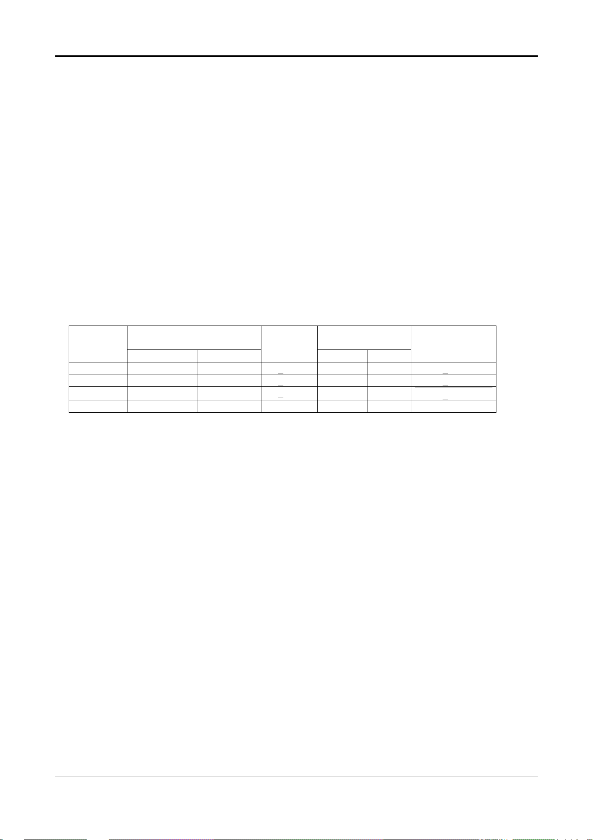
Item Symbol Condition Min. Typ. Max. Unit Note
Contrast Ratio
(Center of screen)
Response
Time
Luminance of White
(Center of screen)
Color
Chromaticity
(CIE 1931)
Viewing
Angle
Brightness Uniformity
(9 points)
Rising TR - 15 30
Falling T
Red
Green
Blue
White
Hor.
Ver.
CR
F - 10 25
Y
L
Rx 0.648
Ry 0.346
Gx 0.292
Gy 0.602
Bx 0.150
By 0.130
Wx 0.313
Wy
θ
L
θ
R
φ
H
φ
L
B
UNI
Normal
φ
θ
Viewing
Angle
CR≥10
T.B.D 500 -
= 0˚
= 0˚
70 - -
200 250 -
TYP.
-0.03
0.329
85 - 85 - 85 - 85 - -
TYP.
+0.03
msec
cd/m2
Degrees
%
(1)(2)(4)
BM-5A
(1)(3)
BM-7
(5)
BM-5A
(1)(4)
PR650
(1)(4)
BM-5A
(6)
BM-5A
Note 1) Definition of Viewing Angle: Viewing angle range (10≤CR)
5
Page 6
Note 2) Definition of Contrast Ratio (CR): Ratio of gray max(Gmax),gray min(Gmin) at the
center point of panel.
Luminance with all pixels white (Gmax)
CR=
Luminance with all pixels black (Gmin)
Note 3) Definition of Response time: Sum of T
, TF
R
6
Page 7
Note 4) After stabilizing and leaving the panel alone at a given temperature for 30 min, the
measurement should be executed .Measurement should be executed n a stable,
windless ,and dark room.30 min after lighting the back-light. This should be
measured in the center of screen. Dual lamp current :13.0mA(6.5mA x2)(Refer to
the note(1) in the page 14 for more information ).
Environment condition :Ta=25±2°C
Optical characteristics measurement setup
7
Page 8
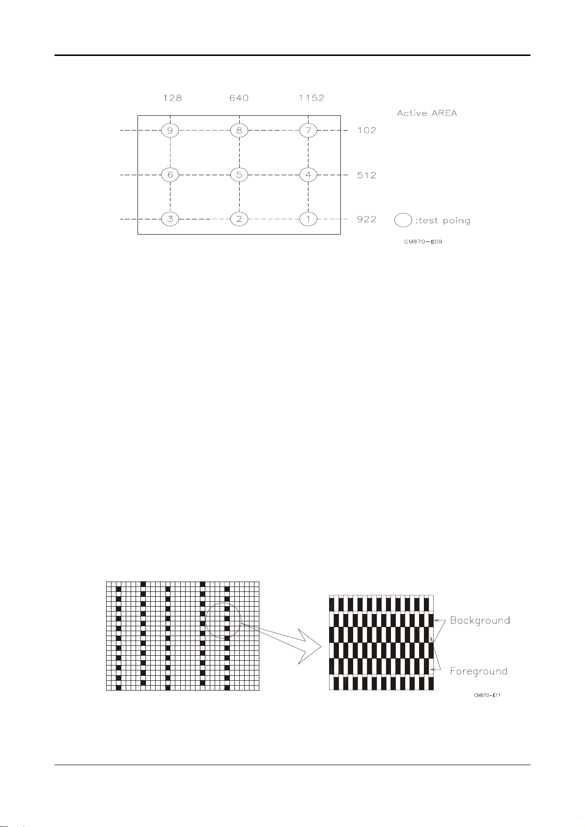
Notes 5) Definition of Luminance of White : measure the luminance of white at center point.
Notes 6)Definition of 9 points brightness uniformity (Measuring points: Refer to the Note 5)
Bmin
B
=100∗∗∗∗
UNI
Bmax
Bmax: Maximum brightness
Bmin: Minimum brightness
Notes 7) Definition of Flicker level
Flicker Voltage
pp
F = x 100 %
LMD Voltage
dc
♦♦♦♦ One maximum value of three estimated values.
♦♦♦♦ For this test ,an LMD(Light Measurement Device)is needed with adequate response time
to track any visible rate flicker component and with a voltage level output proportional
To luminance intensity.
♦♦♦♦ Test Pattern: For dot inversion Driving(Gray levels of foreground dots on the test panel
Are G22,G32,and G45)
♦♦♦♦ Test Point :Center point of the display area
8
Page 9

Note 8) Definition of Crosstalk (Refer to the VESA STD)
The calculation for shadowing is made from the 2 luminance measurements Gbkg and Lsh,
as follows:
Lmax -Lmin
C
= x100 %
T
Lmin
Where Lmax is the larger value of Gbkg or Lsh , and Lmin is the smaller of the two.
♦ To determine background and foreground levels (colors),first set the background to any
gray scale or color level suitable for shadowing determination.(Note that it may take
several iterations of adjusting background level and box levels to determine the proper
value for the background .Next display the box levels to determine the proper value for the
background level. Look for shadowing in any direction from box E. Independently vary the
gray level (or color) of the background and box E until the worst case shadowing is
observed. This defines the background (Gbkg) and foreground (Gfg) levels to be
maintained for the remainder of the test.
♦ One point only (the target) will be measured. To determine that point proceed as follows
Using the background and foreground gray levels of step1 (Gbkg and Gfg). Turn on each
box at a time. Look for the case with the worst shadowing. The box causing the worst case
is the shadowing source, or Bsrc. Use Bsrc and the box opposite from it that lies directly in
the shadow path. That is the target box, or Btgt. Note that box Eight be either Bsrc or Btgt,
depending on the shadowing conditions, but typically Bsrc and Btgt will be a pair of
opposite boxes, A&C or B&D. Btgt will only be displayed for aligning the LMD. It will be
turned off for the actual measurement.
♦♦♦♦ The target box point (Btgt) will be measured with the source box (Bsrc) turned on then off.
(Btgt is for alignment purpose only) Display the background only at level Gbkg. Display
Btgt determined in step 2 above. Using the correct distance, angle, and measurement
aperture, align the LMD to the center of the Btgt. Turn off Btgt. With Gbkg set to its proper
level, measure the luminance (or color). Next,turn on the source box Bsrc. Again measure at
the center point of Btgt (without Btgt present.). In this case the LMD will be measuring the
shadowing level, Lsh.
9
Page 10
2.4 Input Signals
2.4.1 Video input
• Type Analog R, G, B., Digital TMDS
• Input Impedance 75 ohm +/- 2%
• Polarity Positive
• Amplitude 0 - 0.7 +/- 0.05 Vp
• Display Color same as LCD panel
2.4.2 Sync input
• Signal separate horizontal and vertical sync, or composite sync
which are TTL compatible
• Polarity positive and negative.
2.4.3 Interface frequency
The following frequency range is generalized by supported timing. If the entered
mode does not match the supported timing the display optimization will not be
assured.
• Horizontal Frequency 24KHz --80KHz(analog), 31.5– 80KHz(digital)
• Vertical Frequency 56Hz ---------75Hz
DISPLAY MODES
MONITOR
MODE NO.
1 640x350 31.5 + 70.0 - 25.0 VGA
2 640X400 24.83 - 56.4 - 21.05 NEC
3 640X400 31.5- 70.0+ 25.0 VGA
4 640X400 31.5- 70.1- 25.19 NEC
5 640X480 31.5 - 60.0 - 25.0 Defacto
6 640X480 35.0- 66.67- 30.24 MAC
7 640X480 37.86- 72.80- 31.5 VESA
8 640X480 37.5- 75.0- 31.5 VESA
9 720X400 31.5 - 70.0 + 28.0 Text Defacto
10 832X624 49.72- 74.55 - 57.28 MAC
11 800X600 35.16+ 56.25+ 36.0 SVGA
12 800X600 37.8 + 60.0 + 40.0 VESA
13 800X600 48.07 + 72.18 + 50.0 VESA
14 800X600 46.87+ 75.0+ 49.5 VESA
15 1024X768 48.4 - 60.0 - 65.0 VESA
16 1024X768 53.96 + 66.13 + 71.66 XGA
17 1024X768 56.47 - 70.07 - 75.0 VESA
18 1024X768 60.0 + 75.0 + 78.75 VESA
19 1024x768 60.24- 75.02- 80.0 MAC-768
20 1280X1024 64.0 + 60.0 + 108.5 SXGA
21 1280X1024 80.0 + 75.0 + 135.0 Defacto
SCREEN
RESOLUTION
HORIZONTAL
SYNC RATE
(kHz)
VERTICAL
SYNC RATE
(Hz)
VIDEO CLK
(MHz)
STANDARD
10
Page 11

Supported Timing
TIMING
FV(HZ) POLARITY (DOT/LINE) (DOT/LINE) WIDTH PORCH PORCH FOREQ.(MHZ)
(DOT/LINE) (DOT/LINE) (DOT/LINE)
640x350 31.469 + 800 640 96 16 48 25.175
VGA-350 70.087 – 449 350 2 37 60
640x400 24.83 – 848 640 64 64 80 21.05
NEC PC9801 56.42 – 440 400 8 7 25
640x400 31.469 – 800 640 96 16 48 25.175
VGA-GRAPH 70.087 + 449 400 2 12 35
640x400 31.5 – 800 640 64 16 80 25.197
NEC PC9821 70.15 – 449 400 2 13 34
640x480 31.469 – 800 640 96 16 48 25.175
VGA-480 59.94 – 525 480 2 10 33
640x480 35.00 – 864 640 64 64 96 30.24
APPLE MAC480
640x480 37.861 – 832 640 40 16 120 31.5
VESA-480-72Hz 72.809 – 520 480 3 1 20
640x480 37.5 – 840 640 64 16 120 31.5
VESA-480-75Hz 75 – 500 480 3 1 16
720x400 31.469 – 900 720 108 18 54 28.322
VGA-400-TEXT 70.087 + 449 400 2 12 35
832x624 49.725 – 1152 832 64 32 224 57.2832
APPLE MAC800
800x600 35.156 + 1024 800 72 24 128 36
SVGA 56.25 + 625 600 2 1 22
800x600 37.879 + 1056 800 128 40 88 40
VESA-600-60Hz 60.317 + 628 600 4 1 23
800x600 48.077 + 1040 800 120 56 64 50
VESA-600-72Hz 72.188 + 666 600 6 37 23
800x600 46.875 + 1056 800 80 16 160 49.5
VESA-600-75Hz 75 + 625 600 3 1 21
1024x768 48.363 – 1344 1024 136 24 160 65
XGA 60.004 – 806 768 6 3 29
1024x768 53.964 + 1328 1024 176 16 112 71.664
COMPAQ-XGA 66.132 + 816 768 4 8 36
1024x768 56.476 – 1328 1024 136 24 144 75
VESA-768-70Hz 70.069 – 806 768 6 3 29
1024x768 60.023 + 1312 1024 96 16 176 78.75
VESA-768-75Hz 75.029 + 800 768 3 1 28
1024x768 60.24 – 1328 1024 96 32 176 80
APPLE MAC768
1280x1024 64 + 1688 1280 112 48 248 108
VESA-102460Hz
1280x1024 80 + 1688 1280 144 16 248 135
VESA-102475Hz
If the input timing is not a supported timing listed above but within the supported frequency
range (Horizontal: 80KHz,Vertical: 75Hz), this monitor will select a closest mode instead. But
the display quality may not be optimized.
If the input timing over the supported frequency range, a message “Input Signal Out of Range”
will be shown.
FH(KHZ) SYNC TOTAL ACTIVE SYNC FRONT BACK PIXEL
66.67 – 525 480 3 3 39
74.55 – 667 624 3 1 39
75.02 – 803 768 3 3 29
60 + 1066 1024 3 1 38
75 + 1066 1024 3 1 38
11
Page 12
2.4.4 85Hz refresh rate Support
Monitor should display 85Hz refresh rate mode as emergency mode.
Monitor should display “Out of Range” warning menu at this mode.
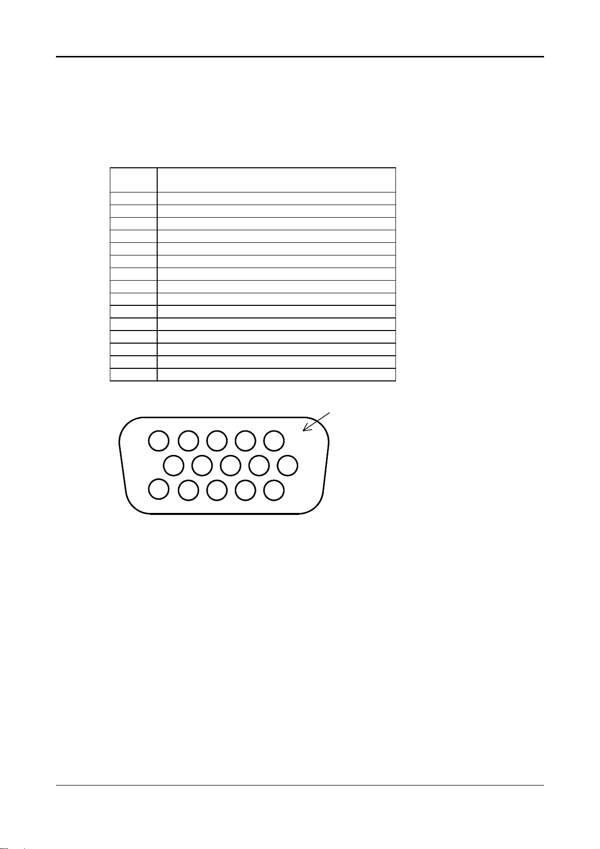
2.4.5 Video input Connector
Analog Video input Connector: 15pins mini D-Sub
Table 2.4.5. Pin assignment for D-sub connector
PIN NO. Separate Sync
1 RED VIDEO
2 GREEN VIDEO
3 BLUE VIDEO
4 GROUND
5 GROUND
6 RED GROUND
7 GREEN GROUND
8 BLUE GROUND
9 PC5V (+5V DDC)
10 CABLE DETECTION
11 GROUND
12 SDA
13 H.SYNC
14 V.SYNC
15 SCL
Color of plastic parts: Blue
5 1
10
15
D-sub connector
6
11
12
Page 13
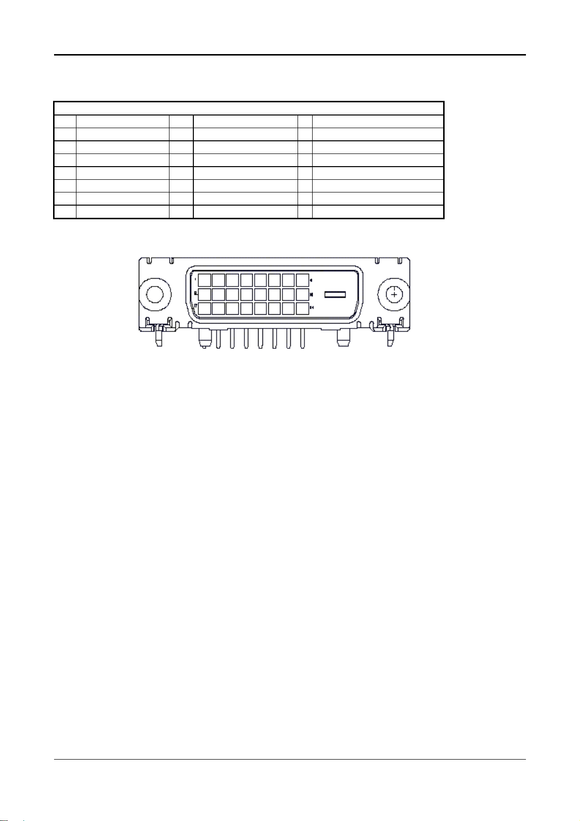
Digital Video input Connector: DVI-D (T.B.D)
Table 4-3-3. Pin assignment for DVI-D (24pin) connector
Pin – Assignment of DVI –D connector :
1 TX2- 9 TX1- 17 TX02 TX2+ 10 TX1+ 18 TX0+
3 Shield (TX2 / TX4) 11 Shield (TX1 / TX3) 19 Shield (TX0 / TX5)
4 NC 12 NC 20 NC
5 NC 13 NC 21 NC
6 DDC-Serial Clock 14 +5V power *) 22 Shield (TXC)
7 DDC-Serial Data 15 Ground (+5V) 23 TXC+
8 No Connect 16 Hot plug detect 24 TXC-
*) In case, the power of the PC unit is switched off and the power of the monitor is switched on,
no voltage may occur at pin 14.
13
Page 14

2.5 CONTROLS
2 3 6 1 4 5
2.5.1 Control panel (monitor front panel)
1. Power LED, will be green when monitor is on; be amber when in power saving mode.
2. Adjust decrease.
3. Adjust increase.
4. Function select counter-clockwise.
5. Function select clockwise.
6. Power ON/OFF switch, push to ON and push to OFF. (toggle switch)
Note: When OSD Menu is off, press button 2 and 3 at the same time can activate “Auto
Adjustment” immediately.
2.5.2 OSD Functions
• OSD Format: Refer to following figure.
• OSD Border: Cyan color
• OSD Tunable Item: The 16 icons that around the border.
• Selected Item: Yellow background
• Comment: Magenta foreground, Blue background
page format :
14
Page 15

Description:
• Brightness: Brightness adjustment, the range from 0 to 100.
• Contrast: Contrast adjustment, the range from 0 to 100.
• H. Position: Horizontal position adjustment.
• V. Position: Vertical position adjustment.
• Phase: Focus adjustment, the range from 0 to 31,32 steps.
• OSD position: OSD position adjustment.
• Auto Adjustment: This feature will automatically adjust size, position, clock and phase.
It takes 3-5 seconds to finish. When auto start, it shows “Auto
Adjusting….” message.
• Clock: Frequency tracking adjustment. The max range from -48 to +48, but
some modes the range will be limited.
• Graph Text: 640x400(GRAPH) or 720x400(TEXT) mode select.
• Language: 5 kinds of language for description, including (English, German,
French, Spanish, Italian)
• Recall: Recall the default value.
• Color Temp: Color temperature for standard 9300,6500, 7500 or user defined.
User:
User R: Red signal gain by user defined.
User G: Green signal gain by user defined.
User B: Blue signal gain by user defined.
7500: Set CIE coordinate at 7500°K color temperature.
6500: Set CIE coordinate at 6500°K color temperature.
9300: Set CIE coordinate at 9300°K color temperature.
• Exit: Exit OSD menu function.
Sharpness : Adjust the scale-up effect(smoother or sharper.)
OSD Transparency: Adjust the transparency level of OSD. The range is from 0 to 100 scales.
Comment:
• 1280x1024: Current mode resolution.
• 60 HZ: Current mode vertical frequency±1Hz.
• VER 1.00: Firmware revision.
15
Page 16
Other features:
Intellectual-Auto LCM999 can start the Auto-Adjustment automatically when input a new
display mode at first time. After the adjustment, LCM999 will remember this mode and
switch to optimized condition automatically for this mode whenever encounter this mode
again. Total 21 recent used modes are recorded into LCM999.
VESA DPMS Functionality When signaled by the host CPU, LCM999 show a black
screen about 3 seconds. If no further signal, then it shows “No Signal” and enter power
saving mode.
2.6 White Color Temperature
White color temperature is 4 preset as 9300, 7500,6500 and User,
Default value of user color should be user which is maximum setting for panel.
Target of color setting
Color
Temp.
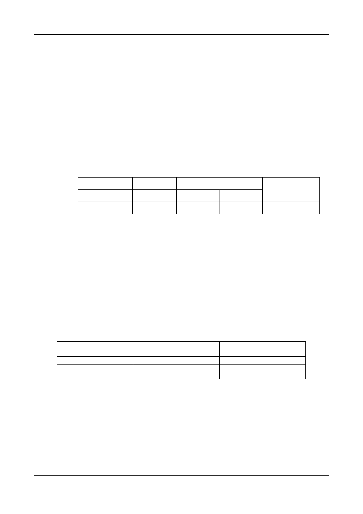
9300K 0.281 0.311 +0.03 0.189 0.446 u’v’ < 0.01*
7500K 0.300 0.315 +0.03 0.194 0.459 u’v’ < 0.01*
6500K 0.315 0.325 +0.03 0.198 0.468
User - - - - -
User should follow “Microsoft Windows Color Quality Specification for Liquid Crystal Display OEM’s”.
(http://www.microsoft.com/hwd ev/tech/color/ColorTest.asp)
Color Coordinate T olerance Color Coordinate Tolerance
x y u’ v’
*) TCO’0X A.2.6.1 requirement
u’v’ <
0.01*
16
Page 17
2.7 POWER SUPPLY
2.7.1 input Voltage Range
The monitor shall operate within specification over the range of 90 to 265 VAC power supply.
2.7.2 Input Frequency Range
Input power frequency range shall be from 47.5 to 63 Hz over the specified input voltage range.
2.7.3 Quick specification review
• Input current
1.5A (max) at 90VAC input and full load ,
0.75A (max) at 264 VAC input and full load.
• Inrush current @ cold start
30A(0-peak)@ 110Vac ,50A(0-peak) @ 220Vac
(measured when switched off for at least 10 mins.)
• Output
Tolerance Output Current
Output Volt - MIN MAX
+12Vdc ±5% 0A 5A 11.4~12.6Vdc
Volt Tolerance
• Total output power: 60 Watt max.
• Withstanding voltage : 1.5Kvac or 2.2KVdc for 1 minute.
• Leakage current : < 0.25mA/100Vac , <3.5mA/230Vac
• Efficiency : 80% min. @115V/230VAC, maximum load.
2.7.4 Power Management
2.7.4.1 Meet VESA DPMS proposal
The monitor must comply with the Microsoft On Now specification, with a minimum of three power
management states, as defined by the VESA DPMS document. The front panel of the monitor must
appropriately display the DPMS state, For example:
DPMS ON : The power LED is Green
DPMS OFF : The power LED is Amber
2.7.5 Power Consumption
On mode 54 Wmax Green
Off mode 4 Wmax Amber
DC power off 4 Wmax Dark
disconnection 4 Wmax
Power saving states are measured with speakers attached but not worked.
The recovery time from stand by /suspend/off mode to on mode is 3 seconds maximun.
Dark (DC power off)
Amber (DC power on)
2.7.6 Power Connector
All units shall have an IEC/CEE-22 type male power receptacle.
2.8 Plug & Play(EDID)
The monitor will be capable of sending a VESA standardized EDID file through the DDC (pins 12,
15 of the VGA connector).
17
Page 18

3. VL-901 DISPLAY CONTROL BOARD
3.1 Description
The VL-901 display control board is design to directly convert the analog RGB signals from
standard VGA display card to optimum LCD timing signals so as to construct a high display
quality LCD monitor.
3.2 Features
•
On board embedded micro-processor to detect display timings and control user
functions.
• Using Genesis gm5120 design to generate optimum LCD timings.
• Using E
2
PROM to memorize every adjusted parameter.
• support up to 22 display modes from VGA to SXGA.
• Offer full screen expansion function on non-SXGA mode (automatic).
• flexible color temperature selection function including 9300,6500,7500 and user
mode.
• Support OSD functions.
• Support VESA DPMS function.
• Support DDC2B functions.
• Support 5 languages for OSD description.
• The longest time for mode change is 3 seconds.
18
Page 19
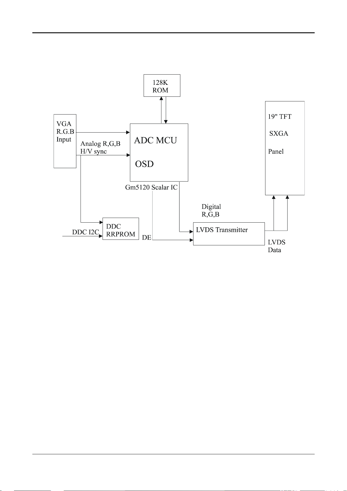
3.3 BLOCK DIAGRAM
19
Page 20

3.4 Connector Locations
3.5 Connector Type
Location Type Maker Number of pins
CN1 74320-4004 MOLEX 24
CN2 1211-15 E&T 15
CN4 6905-40 E&T 40
J1 4300-10 E&T 10
J2 4500-07 E&T 07
3.6 Connector pin assignment
3.6.1 CN2
Pin NO. Signal Comment
1 R-Video Red Video Input.
2 G-Video Green Video Input.
3 B-Video Blue Video Input.
4 N. C.
5 Ground Ground.
6 Ground Ground.
7 Ground Ground.
8 Ground Ground
9 5VCC DDC Power Input.
10 PCDETECT PCDETECT Input.
11 NC NC
12 SDA DDC 2B
13 HS Horizontal Sync Input.
14 VS Vertical Sync Input.
15 SCL DDC 2B
20
Page 21

3.6.2 CN4
Terminal No. Symbol Function
36,37,38 VDD 5V POWER SUPPLY
1 TXE0- LVDS EVEN OUTPUT DATA PAIRS
2 TXE0+ LVDS EVEN OUTPUT DATA PAIRS
4 TXE1- LVDS EVEN OUTPUT DATA PAIRS
5 TXE1+ LVDS EVEN OUTPUT DATA PAIRS
7 TXE2- LVDS EVEN OUTPUT DATA PAIRS
8 TXE2+ LVDS EVEN OUTPUT DATA PAIRS
10 TXECLK- LVDS EVEN OUTPUT DATA PAIRS
11 TXECLK+ LVDS EVEN OUTPUT DATA PAIRS
13 TXE3- LVDS EVEN OUTPUT DATA PAIRS
14 TXE3+ LVDS EVEN OUTPUT DATA PAIRS
16 TXO0- LVDS ODD OUTPUT DATA PAIRS
17 TXO0+ LVDS ODD OUTPUT DATA PAIRS
19 TXO1- LVDS ODD OUTPUT DATA PAIRS
20 TXO1+ LVDS ODD OUTPUT DATA PAIRS
22 TXO2- LVDS ODD OUTPUT DATA PAIRS
23 TXO2+ LVDS ODD OUTPUT DATA PAIRS
25 TXOCLK- LVDS ODD OUT PUT DATA PAIRS
26 TXOCLK+ LVDS ODD OUTPUT DATA PA IRS
28 TXO3- LVDS ODD OUTPUT DATA PAIRS
29 TXO3+ LVDS ODD OUTPUT DATA PAIRS
03,06,09, 12 GND Ground
15, 18, 21, 24 GND Ground
27, 30, 34, 35 GND Ground
39,40 GND Ground
3.6.3 J2
Pin NO. Signal Comment
1,2 5 VCC 5V Power Input
3,4,5 GND GND
6 BLON Bright Light ON/OFF.
7 BRIGHT Brightness Adjustment.
21
Page 22

3.6.4 J1
Pin NO. Signal Comment
1 NC NC
2 LED-Y Power saving mode
3 LED-G Monitor is ON
4 GND GND
5 KEY-POWER Power ON/OFF key
6 KEY-DOWN Function select counter-clockwise key
7 KEY-R Adjust up key
8 KEY-L Adjust down key
9 KEY-UP Function select counter-clockwise key
10 GND GND
3.6.5 CN1 Digital Video input Connector: DVI-D
Pin-Assignment of DVI-D(24 pin) connector
1 TX2- 9 TX1- 17 TX02 TX2+ 10 TX1+ 18 TX0+
3 Shield (TX2 / TX4) 11 Shield (TX1 / TX3) 19 Shield (TX0 / TX5)
4 NC 12 NC 20 NC
5 NC 13 NC 21 NC
6 DDC-Serial Clock 14 -5V Power *) 22 Shield (TXC)
7 DDC-Serial Data 15 Ground (+5V) 23 TXC8 No Connect 16 Hot plug detect 24 TXC+
*)In case, the power of the PC unit is switched off and the power the monitor is switched
on, no voltage may occur at pin 14.
22
Page 23

4. VK901 Control Panel Board
4.1.1 Description
The VK-901 is designed to offer a user interfaced control panel which passes and receives
signals to and from VL-901 display control board.
4.1.2 Connector and Switch Locations
4.1.3 Connector type
Location Type Maker Number of pins
J1 4500-10 E&T 10
4.1.4 Connector pin Assignment
4.1.5 J1
Pin NO. Signal Comment
1 NC NC
2 LED-Y Power saving mode
3 LED-G Monitor is ON
4 GND GND
5 KEY-POWER Power ON/OFF key
6 KEY-DOWN Function select counter-clockwise key
7 KEY-R Adjust up key
8 KEY-L Adjust down key
9 KEY-UP Function select counter-clockwise key
10 GND GND
4.1.6 Switch definition
Location Definition
S5 Power ON/OFF
S1 Function select by clockwise direction
S4 Function select by counter-clockwise direction
S3 Adjust up
S2 Adjust down
4.1.7 LED definition
Location Definition
D1 Green for ON mode; Yellow for OFF mode; yellow for Power Saving
mode; Dark for DC power OFF mode.
23
Page 24

5. INVERTER BOARD
5.1 Description
The Inverter board is designed for lighting up the back-lights of LCD module.
5.2 Electrical characteristics
5.2.1 FOR Fujitsu PANEL FLC48SXC8V
MIN. TYP. MAX. COMMENT
INPUT VOLTAGE 11.4V 12.0V 12.6V 12V±5%
INPUT CURRENT -------- 2A _
Normal BACKLIGHT
VOLTAGE
LAMP CURRENT
DRIVING
FREQUENCY
EFFICIENCY -------- 80% --------
Vin ON/OFF sequence -------- 1s --------
OLP TIME -------- 3S _
BRIGHTNESS
RANGE
Brightness control 0V _ 3.3V
Brightness _ 220cd/m
Strike voltage at 0°C 1600 Vrms _ _
Operating life time 20,000 hrs _ _ (note)
Note:
-------- 700V rms. --------
--------. 7mA rms 8mA rms
KHz 50KHZ KHz
10% -------- 100%
2
_
Vin=12V,
Vbrite=3.3V
Total two lamps for
Unipac
Vin = 12V,max
brightness
Open lamp
protection time
0V, brightness
Life time (hr) can be defined as the time in which it continues to operate under the condition:
Ta=25±2°C, IL =7 mArms until one of the following event occurs:
1. When the brightness becomes 50 %
2. When the startup voltage (Vs) at 0°C becomes higher than the maximal value of Vs specified above.
24
Page 25

5.3 Connector locations
5.3.1 Connector type
J2 J1
J3 J4
CM999-E04
Location Type Maker Number of pins
JN2, JN3, SM02 (8.0)B-BHS ST 2
JN4, JN5
JN1 85205-1200 E&T 12
5.3.2 Connector pin assignment
5.3.2.1 J2,J3,J4,J5
Pin NO. Signal Comment
1 HV High voltage for lamp
J5
5.3.2.2 JN1
Pin NO. Signal Comment
3.3 V for max. brightness (for Fujitsu model)
3 LV Low voltage (common)
1, 2, 3,4 BP+ +12V
7 BLT_ON Back-light ON/OFF control, high active (3.3V)
5, 6, 10, 11, 12 GND
8 +5VS +5VS
9 BRITE BRITE Brightness (0-3.3V) control from I/F
25
Page 26

6. DC/DC POWER and Audio CKT VM-902
6.1 Input:
+12V/5A from AC adapter
6.2 Output:
ITEM Output Voltage Max Load. Min Load Tolerance Ripple & Noise(max)
VCC +5V 2.1A 0.1A ±5 % 200mVpp
6.3 Efficiency: 80 % min at Maximum Load.
6.4 Connector Locations
6.4.1 Connector type for VM-902
Location Type Maker Number of pins
J801 DC-IN SC 2
J802 4500-12 E&T 12
J803 4500-07 E&T 7 (for LCM999 only)
J2 4500-11 E&T 11
6.4.2 Connector pin Assignment
6.4.3 J801 DC 12V Input
Pin No Signal Comment
Pin 1 +12V From adapter output cable
Pin 2 GND From adapter output cable
26
Page 27

6.4.3.1 J802 FOR I/F CKT
Pin No Signal Comment
Pin 1,2,3,4 +12V From adapter +12V power
Pin
5,6,10,11,12
GND GND
Pin 8 +5V Supply for I/F CKT
Pin 7 ON/OFF
Pin 9 BRIGHT
6.4.3.2 J803 FOR M/B CKT
Pin No Signal Comment
Pin 1,2 +5V For M/B +5V power
Pin 3,4,5 GND GND
Pin 6 BLON Bright Light On/ Off
Pin 7 BRIGHT Brightness Adjustment
6.4.3.3 J3 FOR Audio input(for CM999 only)
Pin No Signal Comment
Pin 1 GND GND
Pin 2 Audio IN (1) From Audio output (1)
Pin 3 Audio IN (2) From Audio output (2)
ON/OFF Control ON>3.0V OFF <2.0V
Lamp Current Control (0V to 3.3V) ,
3.3V for max brightness
6.4.3.4 J2 TO Speaker CKT(for CM999 only)
Pin No Signal Comment
Pin 1 VOL Volume ON/OFF control
Pin 2 GND GND
Pin 3 RIN1 Audio volume adjust line INR
Pin 4 LIN1 Audio volume adjust line INL
Pin 5 RIN2 Audio volume a djust line OUTR
Pin 6 LIN2 Audio volume adjust line OUTL
Pin 11 GND
Pin 7 R-EAR EAR phone out R
Pin 8 L-EAR EAR phone out L
Pin 9 ROUT Speaker out R
Pin 10 LOUT Speaker out L
27
Page 28

7. TROUBLESHOOTING
7.1 Main Procedure
28
Page 29

7.1.1 Power Circuit Troubleshooting
29
Page 30

7.1.2 Backlights Troubleshooting
30
Page 31

7.1.3 Performance Troubleshooting
31
Page 32

7.1.4 Function Troubleshooting
32
Page 33

8. MECHANICAL REQUIREMENTS
8.1 Vibration and Shock
All testing shall be done in each of three mutually perpendicular axes, referenced to the
position of the system as it is in front of the user (i.e., front-to back, side-to-side, and top-tobottom).
8.1.1 Non-Operating
The unit should suffer minimal visible cosmetic damage or damage that presents a safety
hazard, or impairs the setup and operation of the system after testing.
Sinusoidal Vibration: 0.75 G zero-to-peak, 10 to 500Hz, 0.5 octave / minute sweep rate.
This requires one sweep, 10 to 500 to 10Hz, along each of the three axes.
Random Vibration: 0.008 G
one hour for each of the three axes.
Half Sine Wave Shock: 120 G peak, half sine pulse, 2 ms pulse duration. Testing shall
consist of one shock in each direction in each axis, for a total of 6 shock inputs.
Square Wave Shock: 40 G peak acceleration, 160 inches / second velocity change. There
shall be one shock in each direction in each axis, for a total of 6 shock inputs.
2
/Hz, 10 to 500 Hz, nominal 2 GRMS. The test shall be for
8.2 Package Drop Specification
Listed below are standards of drop heights for monitor product
Product Weight height Specs
<9.1 kg 0.76 m
9.2~18.2 kg 0.66 m
18.3~27.2 Kg 0.61 m
27.3~45.4 Kg 0.46 m
8.2.1 Drop Test Sequence
Drop Order Drop point Drop Times
1 Right Front Bottom Corner 1
2 Right Bottom Edge 1
3 Right Front Edge 1
4 Front Bottom Edge 1
5 Bottom Side 1
6 Top Side 1
7 Front Side 1
33
Page 34

8 Back Side 1
9 Left Side 1
10 Right Side 1
8.3 Dimension Size and Weight
Dimension size 433 (W) x 447 (H) x 235 (D)
Net Weight 6.5Kg
Gross Weight 8.5Kg
34
Page 35

8.4 Gap Spec.
8.4.1 The step between front bezel and back cover shall be within specification.
Back Cover & Bezel Gap
0.8 mm ≤ A ≤ 1.2 mm
Back Cover & Bezel Alignment
0 mm ≤ D ≤ 0.8 mm
Back Cover & Cable Cover Gap
0.8 mm ≤ B ≤ 1.2 mm
35
Page 36

Back Cover & Cable Cover Gap
0.8 mm ≤ B ≤ 1.2 mm
36
Page 37

Base Cover & Neck Cover Gap
0.8 mm ≤ C ≤ 1.2 mm
8.4.2 LCD Horizontally
The angle between front bezel and LCD unit in bottom side should not be larger than 1.0mm.
37
Page 38

The distance of the LCD display unit from left side to right should not be larger than
E - F<=4.0mm.
Tilt Base Rotation
Tilt up 25 ± 1°/ down 5 ±1°
8.5 Swivel Base Rotation
Swivel Right 45 ±1° / Left 45 ±1°
8.6 Plastic Material
Front Bezel ABS 94HB, 94V-0
Back Cover ABS 94HB, 94V-0
The Others ABS 94HB
TCO’ 99(Optional)
Front Bezel PC + ABS 94 - V0
BACK COVER PC + ABS 94 – V0
The others ABS 94 HB
38
Page 39

8.7 GAP Spec.
Gap between panel with bezel is 0 mm < gap < 1.5 mm
CM999
9. Power Line Transient Test (IEC 61000-4-4 Fast Transients/Burst)
TEST CONDITIONS & PROCEDURE: (Follow IEC 61000-4-4)
Test Condition :
The condition is based on operating with 50Ω load.
39
Page 40

9.1 Peak Voltage:
2 KV (applies the Level 3 typical Industrial Environment” of IEC
61000-4-4)
9.2 Polarity : + / -
9.3 Repetition Frequency of the impulse : 5 KHz.
±±±±
9.4 Rise-Time : 5ns
30%
9.5 Impulse Duration: 50 nS
±±±±
30%
9.6 Relation to Power Supply: Asynchronous
±±±±
9.7 Burst Duration: 15 ms
9.8 Burst Period: 300 ms
20%
±±±±
20%
9.9 Climatic Conditions:
- Ambient Temperature: 15°C to 35°C
- Relative Humidity: 45% to 75%
- Atmospheric Pressure: 86 kPa to 106 kPa
9.10 Test Procedure:
The monitor Display set high-resolution mode, AC input use AC 240V.
Note :
9.10.1
IEC 61000-4-4 defines that power supply, I/O line, and control line all shall be performed
the transient test, but the I/O line and control line is applied with only half of peak voltage
(1 KV).
9.10.2
For the comparison of wave-shape generated by different generator, so the test must uses
a scope with at least 400 MHz bandwidth, and coupled to 50
impulse, duration, and repetition rate of the impulses within one burst.
40
Ω
to monitor the rise-time,
Page 41

WAVESHAPE
41
Page 42

10. Power Line Surge Test (IEC 61000-4-5 Surge)
10.1 Climatic Condition
The climatic conditions shall be within the following ranges:
10.1.1 Ambient Temperature: 15
10.1.2 Relative Humidity: 10% to 75%
10.1.3 Atmospheric Pressure 86kPa(860 mbar)to 106kPa (1060mbar)
Note: The temperature and relative humidity should be recorded in the test report.
°°°°
C to 35
°°°°
C
10.2 Test Conditions:
10.2.1 Wave-shape of the current surge: (refer to IEC 61000-4-5)
Open circuit voltage: (1.2 / 50 µs)
Short circuit current: (8 / 20 µs)
10.2.2 Polarity: positive / negative
10.2.3 Phase shifting:in a range between 0º to 270º versus the AC line phase angle
10.2.4 Repetition rate:at least 1 per minute
10.2.5 Number of tests: at least 5 positive and 5 negative at the selected points.
10.3
The surge will be applied between lines and between lines and ground.
10.4
If not otherwise specified, the surge to power supply circuits shall be applied synchronized
to the voltage phase at the zero crossing and the peak value of the AC voltage wave.
(Positive and negative)
10.5
The surge voltage for test is from 1 KV and increases 1 kV for each step.
10.6
The recommended severity levels for the surge voltage test is 2.0 KV, and without any
degradation or loss of function that is not recoverable due to damage of component or
software allowed.
10.7 Display set high-resolution mode, AC input use AC 240V.
42
42
Page 43

11. ENVIRONMENTAL REQUIREMENTS
11.1 Operating
Temperature 5°C ~ 40°C
Relative Humidity 20% to 80%
Altitude Sea level to 8000ft
11.2 Storage or Shipment
Temperature -20°C ~ +60°C
Relative Humidity 5% to 85%
Altitude Sea level to 40,000ft
11.2.1 TEST PROCEDURE:
• Put in temperature chamber under 60°C Time:24 hours
• Back to room temperature Time: 4 hours
• Put in temperature chamber under -20°C Time:24 hours
• Back to room temperature Time:4 hours
• The process repeat 2 times.
43
Page 44

12. REGULATION COMPLIANCE
12.1 This product comply to the most current revisions of following regulations:
UL/CUL
{UL 1950/ CSA C22.2 NO950}
EN 60950/CB Scheme Safety of Information Technology Equipment including Electrical
MPR 1990:8 Test methods for visual display units.
MPR 1990:10 User handbook for evaluation visual display units.
ISO 9241-3: Ergonomic requirements for office work with visual display terminals
ISO 9241-7: Ergonomic requirements for office work with visual display terminals
ISO 9241-8: Ergonomic requirements for office work with visual display terminals
NUTEK/EPA Requirements of power saving according to NUTEK Spec.
TCO 1999 (option) Requirements for Environmental Labeling of Personal Computers.
TUV/GS Safety regulation for displays work places in the office sector.
FCC 47 CFR, Chapter 1,
Subchapter A, Part 15, Subpart B
Standard fo r Safety of Information Technology Equipment including
Electrical Business Equipment
Business Equipment
(VDTs)-Visual display requirements.
(VDTs)-Requirements for display with reflections.
(VDTs)-Requirements for displayed colours.
803299/94/96, EPA Energy star.
Test methods for Ergonomic, Emission, Energy Efficiency, safety.
A digital device that is marketed for use in a residential environment
not withstanding use in commercial, business and industrial
environments.
CISPR 22 Limits and methods of measurements of radio interference
characteristics of information technology equipment.
CE LVD Directive (73/23/EEC) Safety: EN60950
CE EMC Directive (89/336/EEC)
IEC 61000-4
VCCI (option) Specification for limits and methods of measurement of radio
BSMI (option)
EMI: EN55022 class B
Harmonics: EN61000-3-2
Voltage Fluctuation/Flicker: EN61000-3-3
Immunity: EN55024
IEC 61000-4-2 Electrostatic Discharge
IEC 61000-4-3 Radiated Electromagnetic Field
IEC 61000-4-4 Fast Transients/Burst
IEC 61000-4-5 Surge
IEC 61000-4-6 Conducted Disturbance, Induced by Radio
Frequency Fields
IEC 61000-4-8 Power Frequency Magnetic Field
IEC 61000-4-11 Voltage DIP/Interruption
interference characteristics of information technology equipment.
Class B conformity verification report from the VCCI
CNS 13438, Class B
44
Page 45

12.2 Electrostatics Discharge (ESD)
E.S.D Test
This test follow the IEC 61000-4-2
Discharge Voltage Level :
Criteria Contact Discharge (KV) Air Discharge(KV)
Class C ±4 ±4
Class B ±6 ±8
Class A ±8 ±15
Class A : Temporary degradation or loss of function or performance which requires
operator Intervention or system reset.
Class B : Temporary degradation or loss of function or performance which is self-
recoverable
Class C : Normal performance within the specification limits
Discharge times: 20 times for each discharge point, time interval 1 second.
In the case of acceptance tests, the test program and the interpretation of the test results are
subject to
agreement between manufacturer and user.
The test documentation shall include the test conditions and the test results.
45
Page 46

Ambient temperature : 15°C to 35°C
Relative humidity : 30% to 60%
13. QUALITY AND RELIABILITY
13.1 QUALITY ASSURANCE
Unless otherwise specified in this specification or the applicable purchase order, the supplier shall
be responsible for maintaining a statistical process program or performing inspections that are
sufficient to assure that the parts supplied meet the requirements specified herein.
13.2 RELIABILITY
The product shall have a designed MTBF of greater than 20,000 hours during its useful life.
46
Page 47

Appendix A: PCBA Assembly
47
Page 48

DC-JACK +12V
J801
2
1
104 50V CC5D
C801
L801
BEAD/DIP
104 50V/CC5D
C804
+12V
SI8051S/DIP/TO-220
1
VI
U801
3
CM999 P/B - I/B
H-CON SET
J802
1
2
3
4
5
6
7
10
11
12
J802
10
11
12
8
9
1
2
3
4
5
6
7
8
9
CM988 P/B - I/B
(PIN to PIN)
H-CON-SET
+12V
C802
104 50V CC5D
2
GNDSWVSVEN
45
D803
SB140
1 2
+
C803
470U/16V LOW-ESR
L802
56UH/DIP
D804
SB140
1 2
ZD801
6.2B
+
C810
1000U/10V
+5V
BLKON
C805
104 50V/CC5D
J802
1
2
3
4
5
6
7
8
9
10
11
12
E&T_98115-1203/DIP/2.0mm
E&T_4500-12/DIP/2.0mm
1
2
3
4
5
6
7
8
9
10
11
12
1
2
3
4
5
6
7
8
9
10
11
12
J803
1
2
3
4
5
6
7
E&T_98115-1003/DIP/2.0mm
E&T_4500-07/DIP/2.0mm(CM999)
E&T_4500-10/DIP/2.0mm (CM988)
J803
1
2
3
4
5
6
7
8
9
10
<>
BRIGHTNESS
+5V
BLK_on_off
BRIGHTNESS
Bri_ADJ
No. 0533
Audio and D/D
48
HITACHI
Page 49

LVDS_IF
ER[0..7]
EG[0..7]
EB[0..7]
OR[0..7]
OG[0..7]
OB[0..7]
DVS
DHS
DEN
DCLK
LVDS_EN
LCDON
LVDS_EN
RED+
RED-
GREEN+
GREEN-
BLUE+
BLUE-
RXC+
RXCRX2+
RX2-
RX1+
RX1-
RX0+
RX0-
HS
VS
DDC_SCL
DDC_SDA
HCLK
HFSn
SCL
SDA
PCDETECTA
PCDETECTD
RED+
REDGREEN+
GREENBLUE+
BLUE-
RXC+
RXCRX2+
RX2RX1+
RX1RX0+
RX0-
HS
VS
DDC_SCL
DDC_SDA
HCLK
HFSn
SCL
SDA
gm5115
ER[0..7]
EB[0..7]
RED+
REDGREEN+
GREEN-
BLUE+
BLUE-
RXC+
RXC-
RX2+
RX2RX1+
RX1-
RX0+
RX0-
HSYNC
VSYNC
DDC_SCL
DDC_SDA
HCLK
HFSn
SCL AUDIO_ON
SDA
PCDETECTA
PCDETECTD
LVDS_EN
OR[0..7]
OG[0..7]
KEY DOWN
KEY RIGHT
KEY UP
KEY LEFT
KEY ONOFF
EG[0..7]
OB[0..7]
DVS
DHS
DEN
DCLK
LED_Y
LED_G
ER[0..7]
EG[0..7]
EB[0..7]
OR[0..7]
OG[0..7]
OB[0..7]
DVS
DHS
DEN
DCLK
GPIO8/IRQINn
GPIO21/IRQn
GPIO7
GPIO6
GPIO3/TIMER1
GPIO2/PWM2
GPIO1/PWM1
6. LVDS_IF
Display
ER[0..7]
EG[0..7]
EB[0..7]
OR[0..7]
OG[0..7]
OB[0..7]
DVS
DHS
DEN
DCLK
AUDIO_ON
LED_Y
LED_G
KEY DOWN
KEY RIGHT
KEY UP
KEY LEFT
KEY ONOFF
Power
3. Input Connectors
No. 0533
4. gm5115
PPWR
PBIAS
BRI_ADJ
LCDON
BLKON
GPIO0/PWM0
Ctrl/B VL-901 - VGA Input - 1
49
PPWR
5. Display
PBIAS
BRI_ADJ
7. Power
HITACHI
Page 50

CN1
Shell
Shell
DDC_5V
DVI-D
RX2-
RX2+
GND
RX4-
RX4+
SCL
SDA
VS
RX1-
RX1+
GND
RX3-
RX3+
5V
GND
HP
RX0-
RX0+
GND
RX5-
RX5+
GND
RXC+
RXC-
RED
GRN
BLU
HS
GND
D3 EC10QS04
D4 EC10QS04
D5 EC10QS04
1
2
3
4
5
6
7
8
9
10
11
12
13
14
15
16
17
18
19
20
21
22
23
24
C1
C2
C3
C4
C5
GND
SCL_IN
SDA_IN
DVI_5V
L8 STC222B
STS2125
R1 10K
HOT_PLUG
DVI_5V
12
VGA_5V
12
+5V
12
PCDETECTD
R5 100
R6 100
D1
5.6V
GND
DDC_5V
GND
GND
C1
0.1uF
1
2
3
4
U1
NC
NC
NC
GND
24LC21A
VCC
VCLK
SCL
SDA
R4
47K
8
7
6
5
R2
R3
47K
47K
D2
5.6V
1 3
1 3
RX2- SHT-4
RX2+ SHT-4
RX1- SHT-4
RX1+ SHT-4
RX0- SHT-4
RX0+ SHT-4
RXC+ SHT-4
RXC- SHT-4
DDC_SCL SHT-4
DDC_SDA SHT-4
GND
1
2
3
4
DDC_5V
C2
R7
0.1uF
47K
GND
U2
NC
NC
NC
GND
24LC21A
8
VCC
7
VCLK
6
SCL
5
SDA
3.3V_DVDD
VGA_BLU VGA_GRN
PCDETECTA
R8
R9
47K
47K
D6
D7
5.6V
5.6V
1 3
1 3
GND
NC/ZD1 DALC208SC6
1
6
52
3
4
GND
VGA_RED
VGA_SDA
VGA_SCL
HCLK SHT-4
HFSn SHT-4
R12 100
R15 100
Hsync
CN2
11
12
13
14
15
VGA
Pins 6/7/8 are R/G/B
return lines resp.
Vsync
GND
VGA_5V
C101
0.1uF
S1S2
1
6
2
7
3
8
4
9
5
10
PCDETECTA
GND
VGA_RED
VGA_GRN
VGA_BLU
PCDETECTA
GND
R23
510
R18
75
GND
R21 100
R22 100
C10
220pF
C3 0.01uF
C4 0.01uF
C5 0.01uF
C6 0.01uF
C7 0.01uF
C8 0.01uF
3.3V_DVDD
C120
0.1uF
GND
SN74LVC14APWR
14
U3F
13 12
7
SN74LVC14APWR
14
U3A
1 2
7
SN74LVC14APWR
14
U3E
11 10
7
SN74LVC14APWR
14
U3B
3 4
7
RED+ SHT-4
RED- SHT-4
GREEN+ S HT-4
GREEN- SHT-4
BLUE+ SHT-4
BLUE- SHT-4
VS SHT-4
IN
HS SHT-4
R10 20 1%
R11 56.2 1%
R13 20 1%
R14 56.2 1%
R16 20 1%
R17 56.2 1%
C9
220pF
R20
75
D9
5.6V
1 3
R19
75
D8
5.6V
1 3
No. 0533
Ctrl/B VL-901 - VGA Input - 2
50
HITACHI
Page 51

C11
C12
0.1uF
0.1uF
GND
GND
U5
VCCA0
SCL
SDA
22uF
6.3V
C46
22uF
6.3V
GND
GND
81
7
6
5
Reset
Circuit
C25
0.1uF
C37
0.1uF
C47
0.1uF
GND
C26
0.1uF
C38
0.1uF
C48
100pF
R24
10K
GND
U7
MCP809-300
BAV99L SIZE
+3.3V
L1
BLM21P300S C24
+2.5V 2.5V_AVDD
L3
BLM21P300S
3.3V_DVDD
C51
0.1uF
2
A1A2WP
3
4
GND
AT24C16-10SC-1.8
GND
C13
0.1uF
C27
0.1uF
C39
0.1uF
R25
10K
SCL
RMADDR[0..15]
RMADDR15
RMADDR14
RMADDR13
RMADDR12
RMADDR11
RMADDR10
RMADDR9
RMADDR8
RMADDR7
RMADDR6
RMADDR5
RMADDR4
RMADDR3
RMADDR2
RMADDR1
RMADDR0
SW1
SW PUSHBUTTON
3
VCC
2
Reset
1
GND
R30 NC/10K
R31 10K
R32 NC/10K
R33 NC/10K
R34 NC/10K
R35 NC/10K
R36 10K
R37 10K
R40 NC/10K
R41 NC/10K
R42 NC/10K
R43 NC/10K
R44 NC/10K
R45 NC/10K
R46 NC/10K
R47 NC/10K
3.3V_DVDD
GND
C14
0.1uF
C28
0.1uF
C40
0.1uF
C15
0.1uF
C29
0.1uF
C41
0.1uF
3.3V_DVDD
RM-15
RM-14
OSC-SEL
RM-A12
RM-A11
RM-A10
OCM-START
H-PORT-EN
H-PROTO
SCLPOL
RM-A5
RM-A4
RM-A3
RM-A2
RM-A1
RM-A0
/RESET
C16
0.1uF
C30
0.1uF
C42
0.1uF
C17
0.1uF
C31
0.1uF
C43
0.1uF
C18
0.1uF
C32
0.1uF
C44
0.1uF
C19
0.1uF
2.5V_VDD
A17
A16
C20
0.1uF
C33
0.1uF
C45
0.1uF
R29 NC/0
+5V
R38
10K
C34
0.1uF
3.3V_AVDD
R39
10K
R48 10K
C21
0.1uF
C35
0.1uF
C49
22pF
3.3V_DVDD
C22
0.1uF
3.3V_AVDD
C36
0.1uF
X1
14.318MHz
+5V
RMADDR15
RMADDR14
RMADDR13
RMADDR12
RMADDR11
RMADDR10
RMADDR9
RMADDR8
RMADDR7
RMADDR6
RMADDR5
RMADDR4
RMADDR3
RMADDR2
RMADDR1
RMADDR0
FLASH_OEn
3.3V_AVDD
R2810K
GND
C50
22pF
XTAL
R26
0R
/WR
U6 AT49HF/F010-45JC
31
WE
30
NC/A17
2
A16
3
A15
29
A14
28
A13
4
A12
25
A11
23
A10
26
A9
27
A8
5
A7
6
A6
7
A5
8
A4
9
A3
10
A2
11
A1
12
A0
24
OE
22
CE
32-Pin PLCC Socket
DQ7
DQ6
DQ5
DQ4
DQ3
DQ2
DQ1
DQ0
VCC
GND
CVSS
135
148
144
VDD_DPLL_3.3
VDD_SDDS_3.3
CVSS
202
123
3.3V_DVDD
22053678197111
139
RVDD
RVDD
VDD_DDDS_3.3
GND1_ADC
GND2_ADC
GND_RX2
GND_RX1
156
154
177
183
129
37
RVDD
RVDD
RVDD
RVDD
RVDD
RVDD
RVDD
DCLK
PD47/OB7
PD46/OB6
PD45/OB5
PD44/OB4
PD43/OB3
PD42/OB2
PD41/OB1
PD40/OB0
PD39/OG7
PD38/OG6
PD37/OG5
PD36/OG4
PD35/OG3
PD34/OG2
PD33/OG1
PD32/OG0
PD31/OR7
PD30/OR6
PD29/OR5
PD28/OR4
PD27/OR3
PD26/OR2
PD25/OR1
PD24/OR0
PD23/EB7
PD22/EB6
PD21/EB5
PD20/EB4
PD19/EB3
PD18/EB2
PD17/EB1
PD16/EB0
PD15/EG7
PD14/EG6
PD13/EG5
PD12/EG4
PD11/EG3
PD10/EG2
PD9/EG1
PD8/EG0
PD7/ER7
PD6/ER6
PD5/ER5
PD4/ER4
PD3/ER3
PD2/ER2
PD1/ER1
PD0/ER0
TCON_OSP
TCON_OPOL
TCON_OINV
TCON_ESP
TCON_EPOL
TCON_EINV
TCON_RSP2
TCON_RSP3
TCON_RCLK
GPIO10/TCON_ROE3
GPIO9/TCON_ROE2
TCON_ROE
GPIO4/UART_D1
GPIO5/UART_D0
GPIO13/NVRAM_SCL
GPIO12/NVRAM_SDA
GPIO21/IRQINn
GPIO21/IRQn
GPIO7/TCON_TDIV
GPIO6/TCON_SHC
GPIO3/TIMER1
GPIO2/PWM2
GPIO1/PWM1
GPIO0/PWM0
CLKOUT
Int_Test
Reserved
Reserved
GND_RX0
VSS_DPLL
VSS_SDDS
VSS_DDDS
189
147
143
138
+3.3V
DEN
DVS
DHS
BLM21P300S
118
115
117
116
110
109
108
107
106
105
104
103
102
101
100
99
96
95
94
93
92
91
90
87
86
85
84
83
80
79
78
77
76
75
74
73
72
71
70
69
66
65
64
63
62
61
60
59
58
57
56
55
119
120
121
122
123
124
125
126
127
49
48
128
44
45
52
51
39
4
47
46
43
42
41
40
201
200
N/C
142
N/C
132
131
L2
R63 0
R65 0
R64 0
OB7
OB6
OB5
OB4
OB3
OB2
OB1
OB0
OG7
OG6
OG5
OG4
OG3
OG2
OG1
OG0
OR7
OR6
OR5
OR4
OR3
OR2
OR1
OR0
EB7
EB6
EB5
EB4
EB3
EB2
EB1
EB0
EG7
EG6
EG5
EG4
EG3
EG2
EG1
EG0
ER7
ER6
ER5
ER4
ER3
ER2
ER1
ER0SDA
LVDS_EN
RXD
TXD
GPIO13/NVRAM_SCL
GPIO12/NVRAM_SDA
GPIO8/IRQINn
GPIO21/IRQn
GPIO7
GPIO6
GPIO3/TIMER1
GPIO2/PWM2
GPIO1/PWM1
GPIO0/PWM0
GND
DCLK SHT-5,6
DEN SHT-5,6
DVS SHT-5,6
DHS SHT-5,6
OB[0..7] SHT-5,6
OG[0..7] SHT-5,6
OR[0..7] SHT-5,6
EB[0..7] SHT-5,6
EG[0..7] SHT-5,6
ER[0..7] SHT-5,6
LVDS_EN
AUDIO_ON SHT- 5
SCL SHT-3
SDA SHT-3
LED_Y SHT-5
LED_G SHT- 5
KEY DOWN
KEY RIGHT
KEY ONOFF SHT-5
KEY LEFT SHT-5
KEY UP SHT -5
BRI_ADJ SHT-5
SHT-5
SHT-5
SHT-5
2.5V_VDD
3.3V_AVDD
2.5V_AVDD
3.3V_DVDD
R66
R67
10K
10K
GND
PPWRSHT-5
PBIASSHT-7
TCLK
PCDETECTASHT-3
PCDETECTDSHT-3
HFSnSHT-3
HCLKSHT-3
DDC_SCLSHT-3
DDC_SDASHT-3
RED+SHT-3
RED-SHT-3
GREEN+SHT-3
GREEN-SHT-3
BLUE+SHT-3
BLUE-SHT-3
HSYNCSHT-3
VSYNCSHT-3
RXC+SHT-3
RXC-SHT-3
RX2+SHT-3
RX2-SHT-3
RX1+SHT-3
RX1-SHT-3
RX0+SHT-3
RX0-SHT-3
RMDATA7
21
RMDATA6
20
RMDATA5
19
RMDATA4
18
RMDATA3
17
RMDATA2
15
RMDATA1
14
RMDATA0
13
+5V+5V
1
NC
32
16
GND
3.3V_DVDD
RMDATA[0..7]
LCDON
BLKON
TCLK
XTAL
A17
A16
/RESET
R27 1K
RMADDR15
RMADDR14
RMADDR13
RMADDR12
RMADDR11
RMADDR10
RMADDR9
RMADDR8
RMADDR7
RMADDR6
RMADDR5
RMADDR4
RMADDR3
RMADDR2
RMADDR1
RMADDR0
RMDATA7
RMDATA6
RMDATA5
RMDATA4
RMDATA3
RMDATA2
RMDATA1
RMDATA0
ROM_OEn
gm5115 Family
+5V
C52
0.1uF
GND
PQFP208
141
146
150
173
181
187
193
196
164
168
172
160
199
175
178
184
190
197
198
157
158
161
165
169
149
145
140
113
114
152
151
206
207
208
205
204
171
170
167
166
163
162
137
136
159
194
195
179
180
185
186
191
192
174
1%
U4
AVDD_DDDS
AVDD_SDDS
AVDD_RPLL
AVDD_IMB
AVDD_RX2
AVDD_RX1
AVDD_RX0
AVDD_RXC
AVDD_BLUE
AVDD_GREEN
AVDD_RED
AVDD_ADC
VDD_RXPLL_2.5
AGND_IMB
AGND_RX2
AGND_RX1
AGND_RX0
AGND_RXC
AGND_RXPLL
SGND_ADC
AGND_ADC
AGND_BLUE
AGND_GREEN
AGND_RED
AVSS_RPLL
AVSS_SDDS
AVSS_DDDS
PPWR
PBIAS
TCLK
XTAL
GPIO20
GPIO19
GPIO18
1
GPIO17
GPIO16/HFSn
GPIO22/HCLK
6
DDC_SCL
7
DDC_SDA
5
RESETn
50
GPIO11/ROM_WEn
RED+
REDGREEN+
GREENBLUE+
BLUEHSYNC
VSYNC
ADC_TEST
RXC+
RXCRX2+
RX2RX1+
RX1RX0+
RX0-
REXT
8
ROM_ADDR15
9
ROM_ADDR14
10
ROM_ADDR13
11
ROM_ADDR12
12
ROM_ADDR11
13
ROM_ADDR10
14
ROM_ADDR9
15
ROM_ADDR8
16
ROM_ADDR7
17
ROM_ADDR6
18
ROM_ADDR5
19
ROM_ADDR4
22
ROM_ADDR3
23
ROM_ADDR2
24
ROM_ADDR1
25
ROM_ADDR0
28
ROM_DATA7
29
ROM_DATA6
30
ROM_DATA5
31
ROM_DATA4
32
ROM_DATA3
33
ROM_DATA2
34
ROM_DATA1
35
ROM_DATA0
36
ROM_OEn
153
VDD2_ADC_2.5
3.3V_A
AGND
RVSS
RVSS
RVSS
3213854688298
GND
155
176
182
188
VDD_RX2_2.5
VDD_RX1_2.5
VDD_RX0_2.5
VDD1_ADC_2.5
RVSS
RVSS
RVSS
RVSS
112
TXD
RXD
2688134
203
CVDD_2.5
CVDD_2.5
CVDD_2.5
CVDD_2.5
RVSS
RVSS
CVSS
CVSS
CVSS
13089133
27
NC/CN3 E&T 96113-0512
4
No. 0533
Ctrl/B VL-901 - VGA Input - 3
51
HITACHI
Page 52

SHT-4
SHT-4
SHT-4
KEY UP
KEY LEFT
KEY ONOFF
KEY RIGHTSHT-4
KEY DOWNSHT-4
3.3V_DVDD
R50
470
C53
0.1uF
GND
R51
470
C54
0.1uF
R52
470
C55
0.1uF
R53
470
C56
0.1uF
R54
470
R72 100
R73 100
R71 100
R74 100
R75 100
C57
0.1uF
+5V
SHT-4
SHT-4
LED_Y
LED_G
R56
47K / 4.7K
R59
47K / 4.7K
3.3V_DVDD
B
3.3V_DVDD
B
E
Q1
C
2N3906 / NC
E
Q2
C
2N3906 / NC
R61 75 / 100
SHT-4
AUDIO_ON
NC/4.7uF/10V 0805
GND GND
C63
470pF
GND GND
C58
C64
470pF
R55 NC/820
C59
NC/0.1uF
KEY ONOFF
KEY DOWN
KEY RIGHT
KEY LEFT
KEY UP
GND
J1
1
2
3
4
5
6
7
Keyboard Connector
8
9
10
Molex_53261-1090
PANEL_VDD
PANEL_VDD
C62
18pF
GND
GND
U8
1
S1
2
S2
3
S3
4 5
GD 1
SI9435_SO8
Q3
2SC2411K
8
D4
7
D3
6
D2
L4 BLM21P300S
C61
+
47uF
C60
680uF/16V DIP
GND
PPWRSHT-4
LCDON
R60 10K
+
C65
NC/47uF
R57
10KR58 75 / 100
+
GND
No. 0533
Ctrl/B VL-901 - VGA Input - 4
52
HITACHI
Page 53

LCDONSHT-4
LCDON
ER0
ER1
ER2
ER3
ER4
ER5
ER6
ER7
EB0
EB1
EB2
EB3
EB4
EB5
EB6
EB7
EG0
EG1
EG2
EG3
EG4
EG5
EG6
EG7
OR0
OR1
OR2
OR3
OR4
OR5
OR6
OR7
OB0
OB1
OB2
OB3
OB4
OB5
OB6
OB7
OG0
OG1
OG2
OG3
OG4
OG5
OG6
OG7
DHS
DVS
DEN
DCLK
RP1 22
8
7
6
8
7
6
RP2 22
RP5 22
8
7
6
8
7
6
RP6 22
RP3 22
8
7
6
8
7
6
RP4 22
RP7 22
8
7
6
8
7
6
RP8 22
RP11 22
8
7
6
8
7
6
RP12 22
RP9
8
7
6
8
7
22
6
RP10 22
U9
DS90CF383MTD
DARED0
DARED1
R62
100
DARED2
DARED3
DARED4
DARED5
DARED6
DARED7
DAGRN0
DAGRN1
DAGRN2
DAGRN3
DAGRN4
DAGRN5
DAGRN6
DAGRN7
DABLU0
DABLU1
DABLU2
DABLU3
DABLU4
DABLU5
DABLU6
DABLU7
DHS
DVS
DEN
DISP_CLK
DARED0
1
DARED1
2
DARED2
3
DARED3
45
DARED4
1
DARED5
2
DARED6
3
DARED7
45
DABLU0
1
DABLU1
2
DABLU2
3
DABLU3
45
DABLU4
1
DABLU5
2
DABLU6
3
DABLU7
45
DAGRN0
1
DAGRN1
2
DAGRN2
3
DAGRN3
45
DAGRN4
1
DAGRN5
2
DAGRN6
3
DAGRN7
45
DCLK
DBRED0
1
DBRED1
2
DBRED2
3
DBRED3
45
DBRED4
1
DBRED5
2
DBRED6
3
DBRED7
45
DBBLU0
1
DBBLU1
2
DBBLU2
3
DBBLU3
45
DBBLU4
1
DBBLU5
2
DBBLU6
3
DBBLU7
45
DBGRN0
1
DBGRN1
2
DBGRN2
3
DBGRN3
45
DBGRN4
1
DBGRN5
2
DBGRN6
3
DBGRN7
45
10pF
C74
LVDS_GND
GND
DBRED0
DBRED1
DBRED2
DBRED3
DBRED4
DBRED5
DBRED6
DBRED7
DBGRN0
DBGRN1
DBGRN2
DBGRN3
DBGRN4
DBGRN5
DBGRN6
DBGRN7
DBBLU0
DBBLU1
DBBLU2
DBBLU3
DBBLU4
DBBLU5
DBBLU6
DBBLU7
DHS
DVS
DEN
DISP_CLK
50
2
51
52
54
55
56
3
8
10
4
6
7
11
12
14
16
18
15
19
20
22
23
24
25
27
28
30
31
TXIN27
TXIN5
TXIN0
TXIN1
TXIN2
TXIN3
TXIN4
TXIN6
TXIN10
TXIN11
TXIN7
TXIN8
TXIN9
TXIN12
TXIN13
TXIN14
TXIN16
TXIN17
TXIN15
TXIN18
TXIN19
TXIN20
TXIN21
TXIN22
TXIN23
TXIN24
TXIN25
TXIN26
TXCLKIN
U10
DS90CF383MTD
TSSOP56
50
TXIN27
2
TXIN5
51
TXIN0
52
TXIN1
54
TXIN2
55
TXIN3
56
TXIN4
3
TXIN6
8
TXIN10
10
TXIN11
4
TXIN7
6
TXIN8
7
TXIN9
11
TXIN12
12
TXIN13
14
TXIN14
16
TXIN16
18
TXIN17
15
TXIN15
19
TXIN18
20
TXIN19
22
TXIN20
23
TXIN21
24
TXIN22
25
TXIN23
27
TXIN24
28
TXIN25
30
TXIN26
31
TXCLKIN
1917
VVV
ODD
26
V
1917
VVV
EVEN
PWRDWN
TXOUT0-
TXOUT0+
TXOUT1-
TXOUT1+
TXOUT2-
TXOUT2+
TXOUT3-
TXOUT3+
TXCLKOUT-
TXCLKOUT+
LVDSVCC
LVDSGND
LVDSGND
LVDSGND
PLLVCC
PLLGND
PLLGND
GND
GND
GND
GND
GND
C75
0.1uF
26
V
TXCLKOUT-
TXCLKOUT+
PWRDWN
TXOUT0+
TXOUT1+
TXOUT2+
TXOUT3+
LVDSVCC
LVDSGND
LVDSGND
LVDSGND
DHSSHT-4
DVSSHT-4
DENSHT-4
DCLKSHT-4
ER[0..7]SHT-4
EB[0..7]SHT-4
EG[0..7]SHT-4
OR[0..7]SHT-4
OB[0..7]SHT-4
OG[0..7]SHT-4
ER[0..7]
EB[0..7]
EG[0..7]
OR[0..7]
OB[0..7]
OG[0..7]
C66
0.1uF
32
48
47
46
45
42
41
38
37
40
39
44
49
43
36
34
35
33
53
29
21
13
5
TXOUT0-
TXOUT1-
TXOUT2-
TXOUT3-
PLLVCC
PLLGND
PLLGND
GND
GND
GND
GND
GND
C76
0.1uF
C67
0.1uF
TXO0TXO0+
TXO1TXO1+
TXO2TXO2+
TXO3TXO3+
TXOCLKTXOCLK+
GND
32
48
47
46
45
42
41
38
37
40
39
44
49
43
36
34
35
33
53
29
21
13
5
C68
0.1uF
C70
0.1uF
C72
0.1uF
LVDS_GND
C77
0.1uF
TXE0TXE0+
TXE1TXE1+
TXE2TXE2+
TXE3TXE3+
TXECLKTXECLK+
C79
0.1uF
C81
0.1uF
GND
C78
0.1uF
GND
LVDS_GND
C69
0.1uF
C71
0.01uF
C73
0.01uF
C80
0.01uF
C82
0.01uF
PANEL SIGNAL OUTPUT
LVDS_ENSHT-4
PANEL_VDD
Connect LVDS grounds to GND
at one single point only.
TXE0TXE0+
TXE1TXE1+
TXE2TXE2+
TXECLKTXECLK+
TXE3TXE3+
TXO0TXO0+
TXO1TXO1+
TXO2TXO2+
TXOCLKTXOCLK+
TXO3TXO3+
PANEL_VDD
LVDS_GNDGND
CN4
1
RXO0-
2
RXO0+
3
GND
4
RXO1-
5
RXO1+
6
GND
7
RXO2-
8
RXO2+
9
GND
10
RXOC-
11
RXOC+
12
GND
13
RXO3-
14
RXO3+
15
GND
16
RXE0-
17
RXE0+
18
GND
19
RXE1-
20
RXE1+
21
GND
22
RXE2-
23
RXE2+
24
GND
25
RXEC-
26
RXEC+
27
GND
28
RXE3-
29
RXE3+
30
GND
31
NC
32
PD
33
NC
34
GND
35
GND
36
VDD
37
VDD
38
VDD
39
GND
40
GND
E&T_6701-40p-0.50m
No. 0533
GND
GND
LVDS_3.3V
Ctrl/B VL-901 - VGA Input - 5
53
HITACHI
Page 54

J2
1
2
3
4
5
6
7
CON7
GND
C90
100uF
GND
+
BLKON
L6
BLM21P300S
PBIAS
C91
0.01uF
5VCC
+5V
+5V
+
U12
APL1117-25uC
C84
0.1uF
ADJ
1
VOVI
VO
GND
23
4
C83
100uF
GND
C92
+
100uF
GND GND GND GND
U11
APL1085-3.3CE
3
IN
OUT
1
GND
C93
0.1uF
+2.5V
+
2
C94
100uF
C87
0.1uF
L7 BLM21P300S
L5 BLM21P300S
C88
0.01uF
GND GND GND
C95
0.1uF
GND GND
+
100uF
2.5V_VDD
C96
+
100uF
C85
C86
0.1uF
3.3V_DVDD+3.3V
C89
+
100uF
47uF
C102
GND
R70 1K
+
BRI_ADJ SHT-4
1
ADJ/GND
1
ADJ/GND
4 Vout
APL1117
SOT-223
2
OUT
4 Vout
APL1085
-33CE
SOT-252
2
OUT
3
IN
3
IN
+5V
C97
100uF
+
GND GND
C98
0.1uF
U13
APL1117-3.3V
VOVI
VO
ADJ
1
GND
23
4
C99
0.1uF
GND GND
+
C100
100uF
LVDS_3.3V
No. 0533
Ctrl/B VL-901 - Power
54
HITACHI
Page 55

Appendix B: DISPLAY UNIT ASSEMBLY
55
Page 56

56
Page 57

57
Page 58

58
Page 59

59
Page 60

THE UPDATED PARTS LIST
FOR THIS MODEL IS
AVAILABLE ON ESTA
Page 61

Hitachi, Ltd. Tokyo, Japan
International Sales Division
THE HITACHI ATAGO BUILDING,
No. 15 –12 Nishi Shinbashi, 2 – Chome,
Minato – Ku, Tokyo 105-8430, Japan.
Tel: 03 35022111
HITACHI EUROPE LTD,
Whitebrook Park
Lower Cookham Road
Maidenhead
Berkshire
SL6 8YA
UNITED KINGDOM
Tel: 01628 643000
Fax: 01628 643400
Email: consumer-service@hitachi-eu.com
HITACHI EUROPE GmbH
Munich Office
Dornacher Strasse 3
D-85622 Feldkirchen bei München
GERMANY
Tel: +49-89-991 80-0
Fax: +49- 89-991 80-224
Hotline: +49-180-551 25 51 (12ct/min)
Email: HSE-DUS.service@hitachi-eu.com
HITACHI EUROPE srl
Via Tommaso Gulli N.39, 20147
Milano, Italia
ITALY
Tel: +39 02 487861
Tel: +39 02 38073415 Servizio Clienti
Fax: +39 02 48786381/2
Email: customerservice.italy@hitachi -eu.com
HITACHI EUROPE S.A.S
Lyon Office
B.P. 45, 69671 BRON CEDEX
FRANCE
Tel: 04 72 14 29 70
Fax: 04 72 14 29 99
Email: france.consommateur@hitachi -eu.com
HITACH EUROPE AB
Egebækgård
Egebækvej 98
DK-2850 Nærum
DENMARK
Tel: +45 43 43 6050
Fax: +45 43 60 51
Email: csgnor@hitachi-eu.com
Hitachi Europe Ltd
Bergensesteenweg 421
1600 Sint- Pieters-Leeuw
BELGIUM
Tel: +32 2 363 99 01
Fax: +32 2 363 99 00
Email: sofie.van.bom@hitachi-eu.com
www.hitachidigitalmedia.com
HITACHI EUROPE S.A.
364 Kifissias Ave. & 1, Delfon Str.
152 33 Chalandri
Athens
GREECE
Tel: 1-6837200
Fax: 1-6835964
Email: service.hellas@hitachi -eu.com
HITACHI EUROPE S.A.
Gran Via Carlos III, 101- 1
08028 Barcelona
SPAIN
Tel: 93 409 2550
Fax: 93 491 3513
Email: atencion.cliente@hitachi -eu.com
HITACHI Europe AB
Box 77 S-164 94 Kista
SWEDEN
Tel: +46 (0) 8 562 711 00
Fax: +46 (0) 8 562 711 13
Email: csgswe@hitachi-eu.com
HITACHI EUROPE LTD (Norway) AB
STRANDVEIEN 18
1366 Lysaker
NORWAY
Tel: 67 5190 30
Fax: 67 5190 32
Email: csgnor@hitachi-eu.com
HITACHI EUROPE AB
Neopoli / Niemenkatu 73
FIN-15140 Lahti
FINLAND
Tel : +358 3 8858 271
Fax: +358 3 8858 272
Email: csgnor@hitachi-eu.com
HITACHI EUROPE LTD
Na Sychrove 975/8
101 27 Praha 10 – Bohdalec
CZECH REPUBLIC
Tel: +420 267 212 383
Fax: +420 267 212 385
Email: csgnor@hitachi-eu.com
 Loading...