

Page 1

SERVICE MANUAL
MANUEL D'ENTRETIEN
WARTUNGSHANDBUCH
CAUTION:
Before servicing this chassis, it is important that the service technician read the “Safety
Precautions” and “Product Safety Notices” in this service manual.
No. 0536
CML176SXW
CML178SXWB
Data contained within this Service
manual is subject to alteration for
improvement.
ATTENTION:
Avant d’effectuer l’entretien du châassis, le technicien doit lire les «Précautions de sécurité»
et les «Notices de sécurité du produit» présentés dans le présent manuel.
VORSICHT:
Vor Öffnen des Gehäuses hat der Service-Ingenieur die „Sicherheitshinweise“ und „Hinweise
zur Produktsicherheit“ in diesem Wartungshandbuch zu lesen.
Les données fournies dans le présent
manuel d’entretien peuvent faire l’objet
de modifications en vue de perfectionner
le produit.
Die in diesem Wartungshandbuch
enthaltenen Spezifikationen können sich
zwecks Verbesserungen ändern.
SPECIFICATIONS AND PARTS ARE SUBJECT TO CHANGE FOR IMPROVEMENT
TFT LCD MONITOR
June 2005
Page 2

EP877/878 TFT LCD MONITOR CONTENTS
1. INTRODUCTION.......................................................................................................................... 4
1.1 Scope ....................................................................................................................................................................4
1.2 Description........................................................................................................................................................... 4
2. ELECTRICAL REQUIREMENTS ................................................................................................. 5
2.1 Standard Test Conditions........................................................................................................................................5
2.2 LCD monitor General specification .....................................................................................................................6
2.3 LCD Panel Specification........................................................................................................ .............................. 7
2.4 Input Signals....................................................................................................................................................... 12
Supported Timing........................................................................................................................................................13
2.5 CONTROLS........................................................................................................................................................15
2.6 White Color Temperature...................................................................................................................................17
2.7 POWER SUPPLY ...............................................................................................................................................18
2.8 Plug & Play(EDID)............................................................................................................................................19
2.9 Audio Technical specification (EP877 Only).....................................................................................................20
3. VL-750 DISPLAY CONTROL BOARD ....................................................................................... 21
3.1 Description......................................................................................................................................................... 21
3.2 Features..............................................................................................................................................................21
3.3 BLOCK DIAGRAM ............................................................................................................................................21
System Block Diagram................................................................................................................................................22
3.4 Connector Locations ..........................................................................................................................................22
3.5 Connector Type ..................................................................................................................................................24
3.6 Signal Pin & Description ...................................................................................................................................24
4. VK-723 Control Panel Board .....................................................................................................25
4.1 Description......................................................................................................................................................... 25
4.2 Connector and Switch Locations........................................................................................................................25
4.3 Connector type....................................................................................................................................................25
4.4 Connector pin Assignment..................................................................................................................................25
4.5 Switch definition.................................................................................................................................................25
4.6 LED definition....................................................................................................................................................25
5. POWER SUPPLY & INVERTER BOARD .................................................................................. 26
5.1 Description......................................................................................................................................................... 26
5.2 Power supply ( AC to DC section)......................................................................................................................26
5.3 Inverter (DC to AC Section)...............................................................................................................................27
5.4 Electrical characteristics....................................................................................................................................27
5.5 Connector locations............................................................................................................................................28
6. TROUBLESHOOTING ............................................................................................................... 30
6.1 Main Procedure.................................................................................................................................................. 30
7. MECHANICAL REQUIREMENTS .............................................................................................. 34
7.1 Vibration and Shock........................................................................................................................................... 34
7.2 Package Drop Specification...............................................................................................................................34
7.3 Dimension Size and Weight................................................................................................................................35
7.4 Gap Spec.............................................................................................................................................................35
7.5 Tilt Base Rotation...............................................................................................................................................36
7.6 Plastic Material..................................................................................................................................................36
7.7 GAP Spec............................................................................................................................................................ 37
8. POWER LINE TRANSIENT TEST (IEC 61000-4-4 FAST TRANSIENTS/BURST) ................... 38
8.1 Peak Voltage: .....................................................................................................................................................38
8.2 Polarity : + / - .............................................................................................................................................38
8.3 Repetition Frequency of the impulse : 5 KHz.....................................................................................................38
8.4 Rise-Time : 5ns ± 30% .....................................................................................................................................38
8.5 Impulse Duration: 50 nS ± 30%.........................................................................................................................38
8.6 Relation to Power Supply: Asynchronous..........................................................................................................38
8.7 Burst Duration: 15 ms ± 20% ............................................................................................................................38
8.8 Burst Period: 300 ms ± 20%..............................................................................................................................38
2
Page 3

8.9 Climatic Conditions: ..........................................................................................................................................38
8.10 Test Procedure: ..................................................................................................................................................38
9. POWER LINE SURGE TEST (IEC 61000-4-5 SURGE) ............................................................ 40
9.1 Climatic Condition .............................................................................................................................................40
9.2 Test Conditions:..................................................................................................................................................40
9.3 .......................................................................................................................................................................40
9.4 .......................................................................................................................................................................40
9.5 .......................................................................................................................................................................40
9.6 .......................................................................................................................................................................40
9.7 Display set high-resolution mode, AC input use AC 240V.................................................................................40
10.ENVIRONMENT REQUIREMENT.............................................................................................. 41
10.1 Operating............................................................................................................................................................41
10.2 Storage or Shipment ...........................................................................................................................................41
11. REGULATION COMPLIANCE .................................................................................................. 42
11.1 This product complies with the most current revisions of following regulations:..............................................42
11.2 Electrostatics Discharge (ESD).......................................................................................................................... 43
12.QUALITY AND RELIABILITY..................................................................................................... 44
12.1 QUALITY ASSURANCE..................................................................................................................................... 44
12.2 RELIABILITY .....................................................................................................................................................44
Appendix A: PCBA ASSEMBLY...................................................................................................... 45
Appendix B: DISPLAY UNIT ASSEMBLY……………………………………………………............... 47
3
Page 4
1. INTRODUCTION
1.1 Scope
This specification defines the requirements for the 17” MICRO-PROCESSOR based Multimode supported high resolution color LCD monitor, This monitor can be directly connected
to general 15 pin D-sub VGA connector and DVI-D digital connector, eliminates the
requirement of optional special display card. It also supports VESA DPMS power
management and plug & play function. There is a build-in stereo audio amplifier with
volume control to drive a pair of speakers.
1.2 Description
The LCD monitor is designed with the latest LCD technology to provide a performance
oriented product with no radiation. This will alleviate the growing health concerns. It is also
a space saving design, allowing more desktop space and comparing to the traditional CRT
monitor, it consumes less power and gets less weight in addition MTBF target is 20K
hours or more.
Comparison Chart of EP877/EP878
CML176SXW CML178SXW B
Panel
Signal Interface DSUB+DVI-D DSUB+DVI-D
Sync Type for analog input Separate / compatible / Separate / compatible /
Color Temp user adjust
DDC
Speaker No 1W +1W
Headphone Jack No Yes
Microphone Jack No No
USB Hub Not supported Not supported
Tilt / Swivel Yes / No Yes / No
Normal 17” panel
Hydis HT17E13-100-110
Support
DDC2B DDC2B
Normal 17” panel
Hydis HT17E13-100-110
Support
4
Page 5

2. ELECTRICAL REQUIREMENTS
2.1 Standard Test Conditions
All tests shall be performed under the following conditions, unless otherwise specified.
Ambient light
Viewing distance
Warrn up time
: 225 lux
: 50cm in front of LCD panel
All specifications : 30 minutes
Fully functional : 5 seconds
Measuring Equipment
: Chroma 2250 signal generator or equivalent, directly
Connected to the monitor under test.
Minolta CA100 photometer, or equivalent
Control settings
User brightness control : Maximum (unless otherwise specified)
User contrast control : Typical (unless otherwise specified)
User red/white balance,
Green/white balance and
Blue/white balance control : In the center (unless otherwise specified )
Power input
: 110Vac or 220Vac
Ambient temperature : 20 ± 5˚C (68 ± 9˚F)
Analog input mode
:1280 x1024 /60Hz
2.1.1 MEASUREMENT SYSTEMS
The units of measure stated in this document are listed below:
1 gamma = 1 nano tesla
1 tesla = 10,000 gauss
cm = in x 2.54
lb = kg x 2.2
degrees F = [°C x 1.8] + 32
degrees C = [°F - 32]/1.8
u' = 4x/(-2x + 12y + 3)
v' = 9y/(-2x + 12y + 3)
x = (27u'/4)/[(9u'/2) - 12v' + 9]
y = (3v')/[(9u'/2) - 12v' + 9]
nits = cd/(m2) = Ft-L x 3.426
lux = foot-candle x 10.76
5
Page 6

2.2 LCD monitor General specification
Panel Type : 17 “ active matrix color TFT LCD
HT17E13-100-110
Display size : 337.92mm (H) x 270.336mm (V)
Display mode : VGA 720 X 400 (70Hz)
VGA 640 X 480 (60/66/70/72/75Hz)
SVGA 800 X 600 (60/70/72/75Hz)
XGA 1024 X 768 (60/70/75Hz)
SXGA 1280 X 1024 (60/75Hz) standard resolution
Pixel pitch : 0.264mm(H) x 0.264mm(V)
Display Dot : 1280 x (RGB) x 1024
Contrast ratio:
Brightness: 300 (Typ)
Response time ( Tr /Tf) : 16ms
Display color : 16.2M (6 bit color + FRC)
Viewing angle: CR>10 L / R : 75/75 (Typ)
U / D : 65/65 (Typ)
Luminance Uniformity : > 75% (minimum)
Pc interface: 1). Video : RGB analog 0.7V peak to peak
Sync : TTL positive or negative
2). Digital TMDS
Signal connector : 15 pin Mini D type, (standard VGA video)
DVI-D connector
3.5mm stereo audio jack (Audio) (EP877)
3.5mm miniature stereo Headphone jack (EP877)
Audio power : 1Wrms + 1Wrms ( 300Hz – 20kHz (S.P.L. – 10 dB))(EP877)
Front control : power on/off with LED select adjustment (+,-)
Interface frequency
θ
= 0˚ 450:1 (Typ)
Horizontal Frequency 24KHz -- 80KHz
Vertical Frequency <75Hz Typ : 60Hz
Plug & Play : Support VESA DDC2B functions
Power Input voltage : Single phase, 50/60HZ, 100VAC to 240VAC ±10%
Total output power : 48 Watt max.
6
Page 7
2.3 LCD Panel Specification
2.3.1 LCD Panel Model ( HydisHT17E13-100-110 )
• Display Type active matrix color TFT LCD
• Resolution 1280 x 1024 pixels
• Display Dot 1280 x (RGB) x 1024
• Display Area 337.92mm(H) x 270.34mm(V)
• Pixel Pitch 0.264mm(H) x 0.264mm(V)
• Display Color 16.2M (6 bit color + FRC)
• Lamp Voltage 700Vrms (typ)
• Lamp Current 6.5 mArms ( typ)
• Weight 1900g ( typ)
• Optical Specifications
Item Symbol Condition
Response time
Contrast Ratio CR
Luminance of white YL
White Uniformity
White Chromaticity
Red Chromaticity
Green Chromaticity
Blue Chromaticity
Vertical
Viewing Angle
Horizontal
Viewing Angle
Rising TR -
Falling T
Up ΘU 60 65 - Deg.
Down Θ
Left ΘL 70 75 - Deg.
Right Θ
Specification
Unit
Min. Typ. Max.
θ
F
δ
Y
Wx 0.270
Wy 0.305
Rx 0.607
Ry 0.317
Gx 0.246
Gy 0.584
Bx 0.113
By
D 60 65 - Deg.
R
= 0˚
θ
= 0˚
θ
= 0˚
75 80 - % -
θ
= 0˚
CR>10
-
350 450 - -
250 300 - Cd/m
0.060
70 75 - Deg.
12 16 ms -
0.300
0.335
0.637
0.347
0.276
0.614
0.143
0.090
0.330
0.365
0.667
0.377
0.306
0.644
0.173
0.120
-
Rema
rk
2
-
-
-
-
-
Cross talk C
T
- - 2.0 % C
T
7
Page 8

Note 1) Definition of Viewing Angle: Viewing angle range (10≤CR)
Note 2) Definition of Contrast Ratio (CR): Ratio of gray max (Gmax), gray min (Gmin) at the
center point of panel.
Luminance with all pixels white (Gmax)
CR=
Luminance with all pixels black (Gmin)
Note 3) Definition of Response time: Sum of T
, TF
R
8
Page 9
Note 4) After stabilizing and leaving the panel alone at a given temperature for 30 min, the
measurement should be executed. Measurement should be executed in a stable,
windless and dark room. 30 min after lighting the back-light. This should be
measured in the center of screen. Dual lamp current :13.0mA (6.5mA x2)(Refer to
note(1) on page 14 for more information).
Environment condition :Ta=25±2°C
Optical characteristics measurement setup
9
Page 10

Notes 5) Definition of Luminance of White : measure the luminance of white at center point.
Notes 6)Definition of 9 points brightness uniformity (Measuring points: Refer to the Note 5)
Bmin
B
=100∗
UNI
Bmax
Bmax: Maximum brightness
Bmin: Minimum brightness
Notes 7) Definition of Flicker level
Flicker Voltage
pp
F = x 100 %
LMD Voltage
dc
♦ One maximum value of three estimated values.
♦ For this test ,an LMD(Light Measurement Device)is needed with adequate response time
to track any visible rate flicker component and with a voltage level output proportional
To luminance intensity.
♦ Test Pattern: For dot inversion Driving(Gray levels of foreground dots on the test panel
Are G22,G32,and G45)
♦ Test Point :Center point of the display area
10
Page 11
Note 8) Definition of Crosstalk (Refer to the VESA STD)
The calculation for shadowing is made from the 2 luminance measurements Gbkg and Lsh,
as follows:
Lmax - Lmin
C
= x100 %
T
Lmin
Where Lmax is the larger value of Gbkg or Lsh , and Lmin is the smaller of the two.
♦ To determine background and foreground levels (colors),first set the background to any
gray scale or color level suitable for shadowing determination. (Note that it may take
several iterations of adjusting background level and box levels to determine the proper
value for the background. Next display the box levels to determine the proper value for the
background level. Look for shadowing in any direction from box E. Independently vary the
gray level (or color) of the background and box E until the worst case shadowing is
observed. This defines the background (Gbkg) and foreground (Gfg) levels to be
maintained for the remainder of the test.
♦ One point only (the target) will be measured. To determine that point proceed as follows
Using the background and foreground gray levels of step1 (Gbkg and Gfg). Turn on each
box at a time. Look for the case with the worst shadowing. The box causing the worst case
is the shadowing source, or Bsrc. Use Bsrc and the box opposite from it that lies directly in
the shadow path. That is the target box, or Btgt. Note that box Eight be either Bsrc or Btgt,
depending on the shadowing conditions, but typically Bsrc and Btgt will be a pair of
opposite boxes, A&C or B&D. Btgt will only be displayed for aligning the LMD. It will be
turned off for the actual measurement.
♦ The target box point (Btgt) will be measured with the source box (Bsrc) turned on then off.
(Btgt is for alignment purpose only) Display the background only at level Gbkg. Display
Btgt determined in step 2 above. Using the correct distance, angle, and measurement
aperture, align the LMD to the center of the Btgt. Turn off Btgt. With Gbkg set to its proper
level, measure the luminance (or color). Next,turn on the source box Bsrc. Again measure
at the center point of Btgt (without Btgt present.). In this case the LMD will be measuring
the shadowing level, Lsh.
11
Page 12

2.4 Input Signals
2.4.1
2.4.2
2.4.3
Video input
• Type Digital / Analog R, G, B.
• Input Impedance 75 ohm +/- 2%
• Polarity Positive
• Amplitude 0 - 0.7 +/- 0.05 Vp
• Display Color same as LCD panel
Sync input
• Signal separate horizontal and vertical sync, or composite sync
which are TTL compatible
• Polarity positive and negative.
Interface frequency
The following frequency range is generalized by supported timing. If the entered
mode does not match the supported timing the display optimization will not be
assured.
• Horizontal Frequency 24KHz --80KHz(analog), 31.5– 80KHz(digital)
• Vertical Frequency 56Hz ---------75Hz
12
Page 13
Supported Timing
TIMING FH(KHZ) SYNC TOTAL ACTIVE SYNC FRONT BACK PIXEL
FV(HZ) POLARITY (DOT/LINE) (DOT/LINE) WIDTH PORCH PORCH FOREQ.(MHZ)
640x350 31.469 + 800 640 96 16 48 25.175
VGA-350 70.087 – 449 350 2 37 60
640x400 24.83 – 848 640 64 64 80 21.05
NEC PC9801 56.42 – 440 400 8 7 25
640x400 31.469 – 800 640 96 16 48 25.175
VGA-GRAPH 70.087 + 449 400 2 12 35
640x400 31.5 – 800 640 64 16 80 25.197
NEC PC9821 70.15 – 449 400 2 13 34
640X480 31.469 - 800 640 96 16 48 25.175
VESA-PAL 50.030 - 629 480 2 62 85
640x480 31.469 – 800 640 96 16 48 25.175
VGA-480 59.94 – 525 480 2 10 33
640x480 35.00 – 864 640 64 64 96 30.24
APPLE MAC-480 66.67 – 525 480 3 3 39
640x480 37.861 – 832 640 40 16 120 31.5
VESA-480-72Hz 72.809 – 520 480 3 1 20
640x480 37.5 – 840 640 64 16 120 31.5
VESA-480-75Hz 75 – 500 480 3 1 16
720x400 31.469 – 900 720 108 18 54 28.322
VGA-400-TEXT 70.087 + 449 400 2 12 35
832x624 49.725 – 1152 832 64 32 224 57.2832
APPLE MAC-800 74.55 – 667 624 3 1 39
800x600 35.156 + 1024 800 72 24 128 36
SVGA 56.25 + 625 600 2 1 22
800x600 37.879 + 1056 800 128 40 88 40
VESA-600-60Hz 60.317 + 628 600 4 1 23
800x600 48.077 + 1040 800 120 56 64 50
VESA-600-72Hz 72.188 + 666 600 6 37 23
800x600 46.875 + 1056 800 80 16 160 49.5
VESA-600-75Hz 75 + 625 600 3 1 21
1024x768 48.363 – 1344 1024 136 24 160 65
XGA 60.004 – 806 768 6 3 29
1024x768 53.964 + 1328 1024 176 16 112 71.664
COMPAQ-XGA 66.132 + 816 768 4 8 36
1024x768 56.476 – 1328 1024 136 24 144 75
VESA-768-70Hz 70.069 – 806 768 6 3 29
1024x768 60.023 + 1312 1024 96 16 176 78.75
VESA-768-75Hz 75.029 + 800 768 3 1 28
1024x768 60.24 – 1328 1024 96 32 176 80
APPLE MAC-768 75.02 – 803 768 3 3 29
1152x864 54.054 + 1480 1152 96 40 192 80
(60Hz) 59.270 + 912 864 3 13 32
1152x864 63.851 + 1480 1152 96 32 200 94.499
(70Hz) 70.012 + 912 864 3 1 44
1152x864 67.50 + 1600 1152 128 64 256 108.00
(75Hz) 75.00 + 900 864 2 2 32
1280x960 60.00 + 1800 1280 112 96 312 108.00
(60Hz) 60.00 + 1000 960 3 1 36
1280x960 70.00 + 1800 1280 112 96 312 126.00
(70Hz) 70.00 + 1000 960 3 1 36
1280x960 75.00 + 1800 1280 112 96 312 135.00
(75Hz) 75.00 + 1000 960 3 1 36
1280x1024 64 + 1688 1280 112 48 248 108
VESA-1024-60Hz 60 + 1066 1024 3 1 38
1280x1024 80 + 1688 1280 144 16 248 135
VESA-1024-75Hz 75 + 1066 1024 3 1 38
Note: Mode 640x350, 640x400 and 720x400 will locate on middle position but cannot be expanded to full screen
on vertical direction.
(DOT/LINE) (DOT/LINE) (DOT/LINE)
13
Page 14
2.4.4
2.4.5
85Hz refresh rate Support
Monitor should display 85Hz refresh rate mode as emergency mode.
Monitor should display “Out of Range” warning menu at this mode.
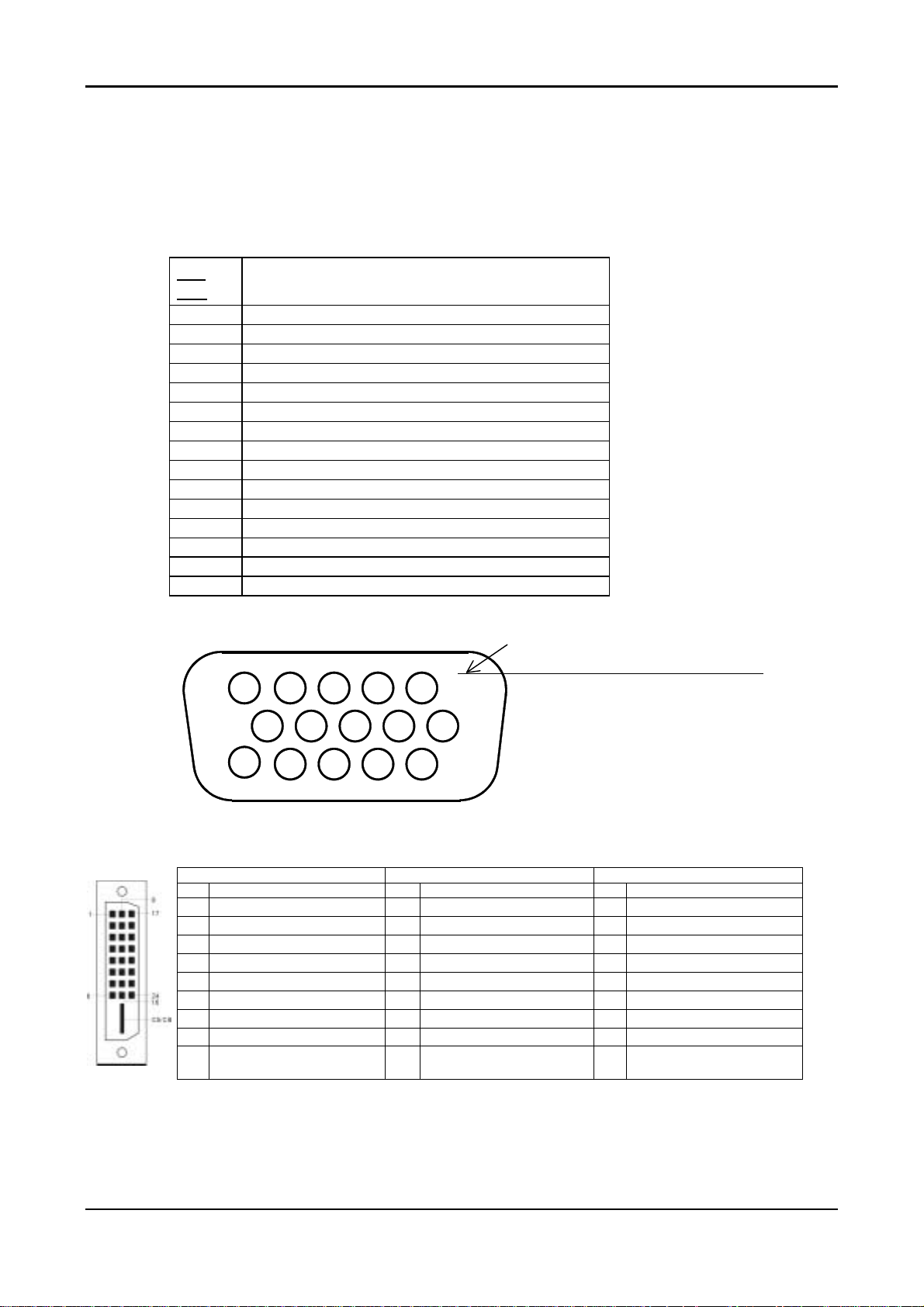
Video input Connector
Analog Video input Connector: 15pins mini D-Sub
Table 2.4.5. Pin assignment for D-sub connector
PIN
NO.
1 RED VIDEO
2 GREEN VIDEO
3 BLUE VIDEO
4 GROUND
5 GROUND
6 RED GROUND
7 GREEN GROUND
8 BLUE GROUND
9 PC5V (+5V DDC)
10 CABLE DETECTION
11 GROUND
12 SDA
13 H.SYNC
14 V.SYNC
15 SCL
Separate Sync
Color of plastic parts: Blue (PC99)
5 1
10
15
D-sub connector
For Digital DVI-D connector
PIN Description PIN Description PIN Description
1 RX2- 10 RX1+ 19 Shield for TMDS Channel 0
2 RX2+ 11 Shield for TMDS Channel 1 20 NC
3 Shield for TMDS Channel 2 12 NC 21 NC
4 NC 13 NC 22 Shield for TMDS Channel clock
5 NC 14 +5V 23 RXC+
6 SCL 15 Hot Plug Detect 24 RXC-
7 SDA 16 HPD C5 NC
8 NC 17 RX0- C6 NC
9 RX1- RX0+
Signal Signal Signal
6
11
14
Page 15

2.5 CONTROLS
2.5.1
2.5.2
Control panel (monitor front panel)
1. Stereo Speakers (EP877)
2. Speaker Volume Control (EP877)
3. Soft Power Switch
4. DC Power-On Indicator
5. Function select Buttons
6. Adjustment Control Buttons
7. External Headphone Jack (EP877)
Note: When OSD Menu is off, press button 2 and 3 at the same time can activate “Auto
Adjustment” immediately.
OSD Functions
• OSD Format: Refer to following figure.
• OSD Border: Cyan color
• OSD Tunable Item: The 16 icons that around the border.
• Selected Item: Yellow background
• Comment: Magenta foreground, Blue background
page format :
15
Page 16

Description:
• Brightness: Brightness adjustment, the range from 0 to 100. Default = 80
• Contrast: Contrast adjustment, the range from 0 to 100. Default = 80
• H. Position: Horizontal position adjustment.
• V. Position: Vertical position adjustment.
• Phase: Focus adjustment, the range from 0 to 100 steps.
• OSD position: OSD position adjustment.
• Auto Adjustment: Press button ( ) to activate the selected function, Auto Adjustment,
Use Analog Input or Use Digital Input.
The Auto Adjustment function let you adjust the display size, clock
and phase to obtain the best viewing settings. This process will take 3
~ 5 seconds to complete. Attention : After Auto Adjustment, the
display might display wrong position or size, if it has received a
pattern which has no screen border. You may select either Analog or
Digital Input video when VGA input or/and DVI Input is/are available.
• Clock: Frequency tracking adjustment. The max range from -50 to +50, but
some modes the range will be limited.
• Graph Text: 640x400(GRAPH) or 720x400(TEXT) mode select.
• Language: 9 kinds of language for description, including (English, German,
French, Spanish, Italian, Pyccknn˜, Japanese , simple Chinese ,
complex Chinese )
• Recall: Recall the default value.
• Color Temp: Color temperature for standard 9300,6500, 7500 or user defined.
User:
User R: Red signal gain by user defined.
User G: Green signal gain by user defined.
User B: Blue signal gain by user defined.
7500: Set CIE coordinate at 7500°K color temperature.
6500: Set CIE coordinate at 6500°K color temperature.
9300: Set CIE coordinate at 9300°K color temperature.
• Exit: Exit OSD menu function.
Sharpness : Adjust the scale-up effect(smoother or sharper.)
OSD Transparency: Adjust the transparency level of OSD. The range is from 0 to 10 scales.
16
Page 17
Comment:
• 1280x1024: Current mode resolution.
• 60 HZ: Current mode vertical frequency±1Hz.
• VER 1.00: Firmware revision.
Other features:
Intellectual-Auto EP877/878 can start the Auto-Adjustment automatically when input a
new display mode at first time. After the adjustment, EP877/878 will remember this mode
and switch to optimized condition automatically for this mode whenever encounter this
mode again. Total 27 recent used modes are recorded into EEPROM
VESA DPMS Functionality When signalled by the host CPU, EP877/878 show a black
screen about 3 seconds. If no further signal, then it shows “No Signal” and enters power
saving mode.
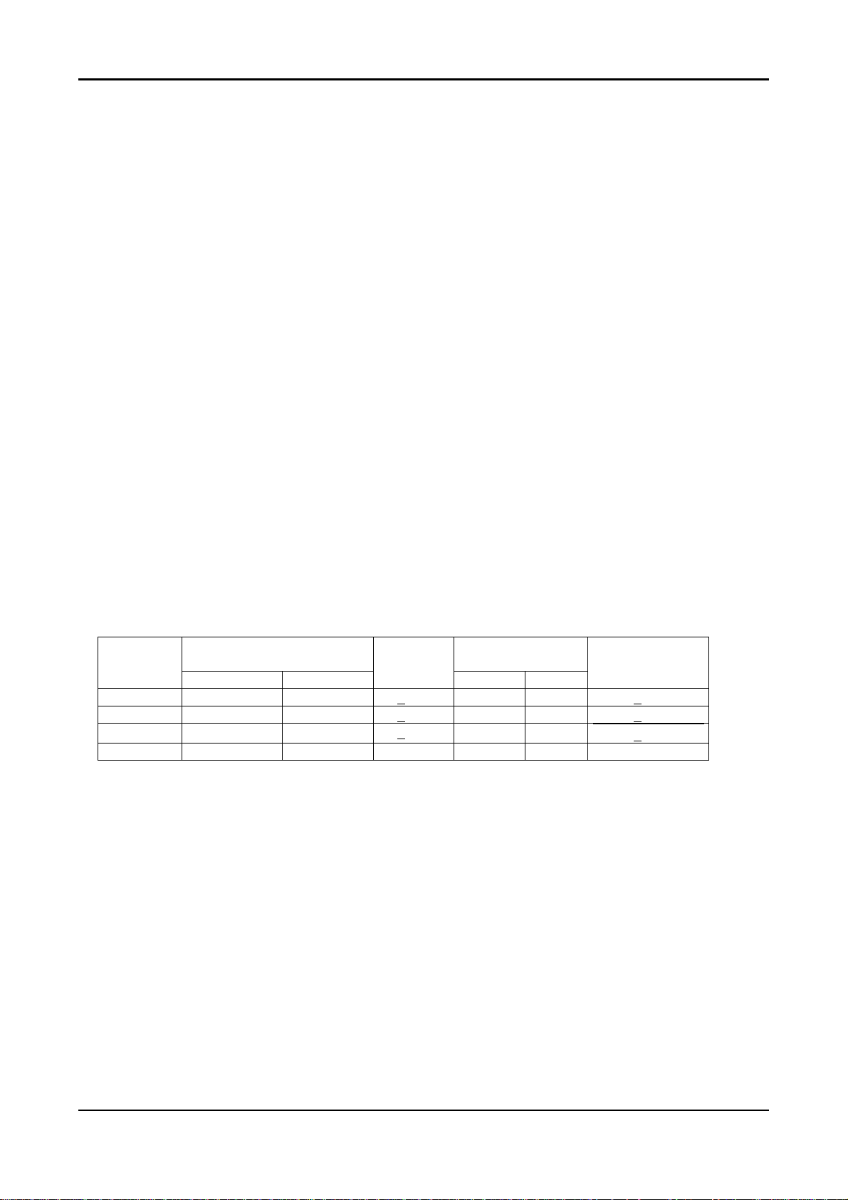
2.6 White Color Temperature
White color temperature is 4 preset as 9300, 7500, 6500 and User,
Default value of user color should be user which is maximum setting for panel.
Target of color setting
Color
Temp.
9300K 0.283 0.297 +0.03 0.189 0.446 u’v’ < 0.01*
7500K 0.299 0.315 +0.03 0.194 0.459 u’v’ < 0.01*
6500K 0.313 0.329 +0.03 0.198 0.468
User - - - - -
User should follow “Microsoft Windows Color Quality Specification for Liquid Crystal Display OEM’s”.
(http://www.microsoft.com/hwdev/tech/color/ColorTest.asp)
Color Co-ordinate Tolerance Color Co-ordinate Tolerance
x y u’ v’
u’v’
*) TCO’0X A.2.6.1 requirement
0.01*
<
17
Page 18
2.7 POWER SUPPLY
2.7.1
2.7.2
2.7.3
input Voltage Range
The monitor shall operate within specification over the range of 90 to 264VAC power supply.
Input Frequency Range
Input power frequency range shall be from 47.5 to 63Hz over the specified input voltage range.
Quick specification review
• Input current
1.2A (max) at 90VAC input and full load ,
0.6A (max) at 264VAC input and full load.
• Inrush current @ cold start
30A (0-peak) @ 110Vac, 50A (0-peak) @ 220Vac
(measured when switched off for at least 10 mins.)
• Output
Tolerance Output Current
Output Volt - MIN MAX
+5Vdc
±5%
0A 1.0A
Volt Tolerance
4.8~5.2Vdc
(for EP877)
+5Vdc
+13Vdc +25%/-10% 0A 2.2A 11.7~16.25Vdc
±5%
0.05A 1.5A 4.8~5.2Vdc
• Total output power: 48 Watt max. for EP877
40 Watt max. for EP878
• Withstanding voltage : 1.5KVac or 2.2KVdc for 1 minute.
• Leakage current : < 0.25mA/100Vac , <3.5mA/230Vac
• Efficiency : 70% min. @ 115V/230Vac, maximum load.
18
Page 19

2.7.4
Power Management
2.7.4.1 Meet VESA DPMS proposal
The monitor must comply with the Microsoft On Now specification, with a minimum of three power
management states, as defined by the VESA DPMS document. The front panel of the monitor must
appropriately display the DPMS state, For example:
DPMS ON : The power LED is Green
DPMS OFF : The power LED is Amber
2.7.5
Power Consumption
On mode
Off mode 3Wmax Amber
DC power off 3Wmax Dark
disconnection 3Wmax
Power saving states are measured with speakers attached but not worked.
The recovery time from stand by /suspend/off mode to on mode is 3 seconds maximun.
2.7.6 Power Connector
All units shall have an IEC/CEE-22 type male power receptacle.
2.8 Plug & Play (EDID)
The monitor will be capable of sending a VESA standardized EDID file through the DDC (pins 12,
15 of the VGA connector).
40Wmax (EP878)
48Wmax (EP877)
Dark (DC power off)
Amber (DC power on)
Green
19
Page 20

2.9 Audio Technical specification (CML178SXW B Only)
2.9.1
General Description:
Output power : 1W + 1W maximum
Total harmonic distortion : Less than 1% (except speakers distortion)
Input signal sensitivity : 0.5Vrms for full output
Input impedance : 47Kohm +/- 5%
Frequency response range : 100Hz – 20KHz (except speakers response)
Difference of L and R output : Less than 2dB
2.9.2
Electrical characteristics (Tamb=25
°
)
Audio amplifier(USE Panasonic VK-723A Audio Analyser. )
Item Audio Input Freq.
Spec.
Comment
Min. Typ. Max.
Input Voltage(V) - 5 -
Input Current(m A) - 500 800
Audio Voltage Gain 500mVrms 1KHz - - 6dB Volume Max.,load 4Ω
Frequency Response 500mVrms 300Hz-20KHz -10dB - +10dB Volume Max.,load 4Ω
Signal to Noise ratio 500mVrms 1KHz - - -40dB Volume Max.,load 4Ω
Total harmonic distortion 500mVrms 1KHz 1% except speakers distortion
Cross talk 500mVrms 1KHz - - -30dB Volume Max.,load 4Ω
Output Watt. 500mVrms 1KHz - - 1W Volume Max.,load 4Ω
Volume Control - - - Analog
2.9.3 Speakers
Maximum power : 1W per speaker (max)
Impedance : 4ohm +/- 15 % @ 1KHz 1.0Hz
Frequency response range : 300Hz – 20KHz (S.P.L. – 10dB)
Total harmonic distortion : Less than 5% @ 0.125W 1KHz
2.9.4
Headphone output
Output power : 1.6mW for 32ohms Headphone
20
Page 21

3. VL-750 DISPLAY CONTROL BOARD
3.1 Description
The VL-750 display control board is design to directly receive R, G, B Analog signal to
optimum LCD timing signals so as to construct a high display quality LCD monitor.
3.2 Features
Support for image expansion and reduction.
•
• On board micro-processor to detect display timings and control user functions.
• Using Novatek design to generate optimum LCD timings.
• Using E
2
PROM to memorize every adjusted parameter.
• Support up to 28 display modes from VGA to SXGA.
• Offer full screen expansion function on non-XGA mode (automatic).
• Support OSD functions.
• Support VESA DPMS function.
• Support DDC2B functions.
• Support English and Japanese language for OSD description.
• The longest time for mode change is 3 seconds.
3.3 BLOCK DIAGRAM
21
Page 22

System Block Diagram
3.4 Connector Locations
22
Page 23

23
Page 24

3.5 Connector Type
Location Type Maker Number of pins
J1 98210-4011 E&T 30
CN302 98115-0313 E&T 3
CN301 4300-11P E&T 11
CN3 96113-0803 E&T 8
CN1 D-SUB E&T 15
CN2 DVI AMP 24
3.6 Signal Pin & Description
3.6.1 CN302
Pin No. Signal Comment
1 Audio-RIN Audio Right Input
2 GND
3 Audio-LIN Audio Left Input
3.6.2 CN301
Pin No. Signal Comment
10 R+ Audio Right+ Output
11 R- Audio Right- Output
3.6.3 CN3
Pin NO. Signal Comment
1 LED-Y Power saving mode
2 LED-G Monitor is ON
3 GND GND
4 KEY-ON/OFF KEY- ON/OFF
5 KEY−UP KEY-Brightness Increase
6 KEY-DOWN KEY-Brightness Decrease
7 KEY-RIGHT KEY-Volume Increase
8 KEY-LEFT KEY-Volume Decrease
1 +5 VDD Audio +5V
2 VR Audio Volume Control
3 L+ Audio Left+ Output
4 L- Audio Left- Output
5 AGND Analog GND
6 HP-S HP-Sense
7 HP-L Audio Left Output (Head Phone)
8 HP-R Audio Right Output (Head Phone)
9 AGND Analog GND
24
Page 25

4. VK-723 Control Panel Board
4.1 Description
The VK-723 is designed to offer a user interfaced control panel which passes and receives
signals to and from VK-723 display control board.
4.2 Connector and Switch Locations
4.3 Connector type
Location Type Maker Number of pins
J4,J1((VK-720) 4301-08 E&T 8
J2 4301-11 E&T 11
J1 87502-0200 ACER 2
J3 87502-0200 ACER 2
JP1 SCJ-0348-C SC 5
4.4 Connector pin Assignment
4.5 Switch definition
Location Definition
S1 Power ON/OFF
S4,S2(VK-720) Function select by clockwise direction
S5,S3(VK-720) Function select by counter-clockwise direction
S2,S4(VK-720) Adjust up
S3,S5(VK-720) Adjust down
4.6 LED definition
Location Definition
D1 Green for ON mode; Yellow for OFF mode; yellow for Power Saving
mode; Dark for DC power OFF mode.
25
Page 26

5. POWER SUPPLY & INVERTER BOARD
5.1 Description
The Power supply and Inverter board is designed for Display control board and lighting up
the back-lights of LCD module.
5.2 Power supply ( AC to DC section)
5.2.1
5.2.2
5.2.3
input Voltage Range
The monitor shall operate within specification over the range of 90 to 264 VAC power supply.
Input Frequency Range
Input power frequency range shall be from 47.5 to 63 Hz over the specified input voltage range.
Quick specification review
• Input current
1.2A (max) at 90VAC input and full load ,
0.6A (max) at 264VAC input and full load.
• Inrush current @ cold start
30A (0-peak) @ 110Vac, 50A (0-peak) @ 220Vac
(measured when switched off for at least 10 mins.)
• Output
Tolerance Output Current
Output Volt - MIN MAX
+5Vdc
±5%
0A 1.0A
Volt Tolerance
4.8~5.2Vdc
(for EP777)
+5Vdc
+13Vdc +25%/-10% 0A 2.2A 11.7~16.25Vdc
±5%
0.05A 1.5A 4.8~5.2Vdc
• Total output power: 48 Watt max. for CML178SXW B
40 Watt max. for CML176SXW
• Withstanding voltage : 1.5KVac or 2.2KVdc for 1 minute.
• Leakage current : < 0.25mA/100Vac, <3.5mA/230Vac
• Efficiency : 70% min. @ 115V/230Vac, maximum load.
26
Page 27

5.3 Inverter (DC to AC Section)
5.4 Electrical characteristics
5.4.1 FOR HYDIX PANEL (HT17E13-100-110)
MIN. TYP. MAX. COMMENT
INPUT VOLTAGE 11.4V 13.0V 16.25V 13V+25% / -10%
INPUT CURRENT -------- 2A --------
Normal BACKLIGHT
VOLTAGE
LAMP CURRENT
(every lamp)
DRIVING
FREQUENCY
EFFICIENCY -------- 75% --------
Vin ON/OFF
sequence
OLP TIME -------- 1S _
BRIGHTNESS
RANGE
Brightness control 0.4V _ 3.3V
Brightness _ 300cd/m
Strike voltage at 0°C 1310Vrms _ _
-------- 700V rms. --------
3mA rms. 6.5mA rms 7mA rms Each CCFL
40KHz 50KHZ 60KHz
-------- 0.5S --------
30% -------- 100%
2
_
Vin=13V,
Vbrite=3.3V
Vin = 13V, max
brightness
Open lamp
protection time
3.3V, brightness
max.
Operating life time 40,000 hrs 50,000 _ (note)
Note:
Life time (hr) can be defined as the time in which it continues to operate under the condition:
Ta=25±2°C, IL =6.5mArms until one of the following event occurs:
1. When the brightness becomes 50%
2. When the startup voltage (Vs) at 0°C becomes higher than the maximal value of Vs specified above.
27
Page 28

5.5 Connector locations
5.5.1 Connector type
-
Location Type Maker Number of pins
J903,J904, J905,J906 SM02B-BHSS-1 JST 2
J802 96113-1203 E&T 10P
P801 SA-4S-066 AC Inlet 3
J701 SCJ03451X9 SC 3
J702 98115-0313 E&T 3
28
Page 29

5.5.2 Connector pin assignment
5.5.2.1 J903, J904, J905, J906
Pin NO. Signal Comment
1 HV High voltage for lamp
2 LV LOW voltage for lamp
5.5.2.2 J802 For Display control board (Interface)
Pin NO. Signal Comment
1 +5Vaudio +5Vdc for Audio ckt
2 GND/Audio Ground for Audio ckt
3,4 GND Common Ground
5 BRITE Brightness adjustable range:
6 N.C.
7 Enable Backlight ON/OFF control (Active High)
0.4V<min>~3.3V<max>
8,9,10 Vcc +5Vdc supply to Interface BD, always on.
5.5.2.3 J701 / J702 For EP877
Pin NO. Signal Comment
1 Audio-RIN Audio Right Input
2 GND
3 Audio-LIN Audio Left Input
ON:1.5~5.5V OFF:-0.3~1.0V.
29
Page 30

6. TROUBLESHOOTING
6.1 Main Procedure
EP877/878
30
Page 31

6.1.1 Power Circuit and Backlights Troubleshooting
31
Page 32

6.1.2 Performance Troubleshooting
32
Page 33

6.1.3 Function Troubleshooting
33
Page 34

7. MECHANICAL REQUIREMENTS
7.1 Vibration and Shock
All testing shall be done in each of three mutually perpendicular axes, referenced to the
position of the system as it is in front of the user (i.e., front-to back, side-to-side, and top-tobottom).
7.1.1
Non-Operating
The unit should suffer minimal visible cosmetic damage or damage that presents a safety
hazard, or impairs the setup and operation of the system after testing.
Sinusoidal Vibration: 0.75G zero-to-peak, 10 to 500Hz, 0.5 octave / minute sweep rate.
This requires one sweep, 10 to 500 to 10Hz, along each of the three axes.
Random Vibration: 0.008G
one hour for each of the three axes.
2
/Hz, 10 to 500Hz, nominal 2 GRMS. The test shall be for
7.2 Package Drop Specification
Listed below are standards of drop heights for monitor product
Product Weight Height Specs
<9.1Kg 0.76m
9.2~18.2Kg 0.66m
18.3~27.2Kg 0.61m
27.3~45.4Kg 0.46m
7.2.1
Drop Test Sequence
Drop Order Drop point Drop Times
1 Right Front Bottom Corner 1
2 Right Bottom Edge 1
3 Right Front Edge 1
4 Front Bottom Edge 1
5 Bottom Side 1
6 Top Side 1
7 Front Side 1
8 Back Side 1
9 Left Side 1
10 Right Side 1
34
Page 35

7.3 Dimension Size and Weight
Dimension size 374 (W) x 387 (H) x 190 (D)
Net Weight 5Kg
Gross Weight 7Kg
7.4 Gap Spec.
7.4.1 The step between front bezel and back cover shall be within specification.
Top Left and Right
Back cover concavity Back cover concavity
0 mm ≤ A ≤ 0.8mm 0 mm ≤ A ≤ 0.8mm
ES678-E04
ES677-E01
35
Page 36

7.4.2 LCD Horizontally
The angle between front bezel and LCD unit in bottom side should not large than 1.0mm.
The angle between front bezel and LCD unit in bottom side should not large than 4.0mm.
7.5 Tilt Base Rotation
Tilt up 30º 2°/ down 5º 2°
7.6 Plastic Material
Front Bezel ABS 94V-0
Back Cover ABS 94V-0
The Others ABS 94HB
TCO’ 99(Optional)
Front Bezel PC + ABS 94 - 5V
BACK COVER PC + ABS 94 – 5V
The others ABS 94 HB
36
Page 37

7.7 GAP Spec.
Gap between panel with bezel is 0 mm < gap < 1.2 mm
ES678-E01
37
Page 38

8. POWER LINE TRANSIENT TEST (IEC 61000-4-4 FAST
TRANSIENTS/BURST)
TEST CONDITIONS & PROCEDURE: (Follow IEC 61000-4-4)
Test Condition :
The condition is base on operating with 50Ω load.
8.1 Peak Voltage:
2 KV (applies the Level 3 typical Industrial Environment” of IEC
61000-4-4)
8.2 Polarity : + / -
8.3 Repetition Frequency of the impulse : 5KHz.
±
8.4 Rise-Time : 5ns
8.5 Impulse Duration: 50nS
30%
±
30%
8.6 Relation to Power Supply: Asynchronous
±
8.7 Burst Duration: 15ms
20%
8.8 Burst Period: 300ms
8.9 Climatic Conditions:
- Ambient Temperature: 15°C to 35°C
- Relative Humidity: 45% to 75%
- Atmospheric Pressure: 86kPa to 106kPa
8.10 Test Procedure:
The monitor Display set high-resolution mode, AC input use AC 240V.
Note :
8.10.1
IEC 61000-4-4 defines that power supply, I/O line, and control line all shall be performed
the transient test, but the I/O line and control line is applied with only half of peak voltage
(1KV).
8.10.2
For the comparison of wave-shape generated by different generator, so the test must uses
a scope with at least 400MHz bandwidth, and coupled to 50
impulse, duration, and repetition rate of the impulses within one burst.
±
20%
Ω
to monitor the rise-time,
38
Page 39

WAVESHAPE
39
Page 40

9. POWER LINE SURGE TEST (IEC 61000-4-5 SURGE)
9.1 Climatic Condition
The climatic conditions shall be within the following ranges:
9.1.1
9.1.2
9.1.3
Ambient Temperature: 15
Relative Humidity: 10% to 75%
Atmospheric Pressure 86kPa (860mbar) to 106kPa (1060mbar)
Note: The temperature and relative humidity should be recorded in the test report.
9.2 Test Conditions:
9.2.1
9.2.2
9.2.3
9.2.4
9.2.5
Wave-shape of the current surge: (refer to IEC 61000-4-5)
Open circuit voltage: (1.2 / 50 µs)
Short circuit current: (8 / 20 µs)
Polarity: positive / negative
Phase shifting:in a range between 0º to 270º versus the AC line phase angle
Repetition rate:at least 1 per minute
Number of tests: at least 5 positive and 5 negative at the selected points.
9.3
The surge will be applied between lines and between lines and ground.
°
C to 35°C
9.4
If not otherwise specified, the surge to power supply circuits shall be applied synchronized
to the voltage phase at the zero crossing and the peak value of the AC voltage wave.
(Positive and negative)
9.5
The surge voltage for test is from 1KV and increases 1KV for each step.
9.6
The recommended severity levels for the surge voltage test is 2.0KV and without any
degradation or loss of function that is not recoverable due to damage of component or
software allowed.
9.7 Display set high-resolution mode, AC input use AC 240V.
40
Page 41

10. ENVIRONMENTAL REQUIREMENT
10.1 Operating
Temperature 5°C ~ 40°C
Relative Humidity 20% to 80%
Altitude Sea level to 8000ft
10.2 Storage or Shipment
Temperature -20°C ~ +60°C
Relative Humidity 5% to 85%
Altitude Sea level to 40,000ft
10.2.1 TEST PROCEDURE
• Put in temperature chamber under 60°C Time:24 hours
• Back to room temperature Time: 4 hours
• Put in temperature chamber under -20°C Time:24 hours
• Back to room temperature Time:4 hours
• The process repeats 2 times.
41
Page 42

11. REGULATION COMPLIANCE
11.1 This product complies with the most current revisions of following
regulations:
UL/CUL Standard for Safety of Information Technology Equipment including
{UL 1950/ CSA C22.2 NO950}
EN 60950/CB Scheme Safety of Information Technology Equipment including Electrical
MPR 1990:8 Test methods for visual display units.
MPR 1990:10 User handbook for evaluation visual display units.
EK1-ITB 2000: Ergonomic requirements for office work with visual display
NUTEK/EPA Requirements of power saving according to NUTEK Spec.
TCO 1999 (option) Requirements for Environmental Labeling of Personal Computers.
Electrical Business Equipment
Business Equipment
terminals (VDTs)-Visual display requirements.
803299/94/96, EPA Energy star.
Test methods for Ergonomic, Emission, Energy Efficiency, safety.
TUV/GS Safety regulation for displays work places in the office sector.
FCC 47 CFR, Chapter 1,
Subchapter A, Part 15, Subpart B
CISPR 22 Limits and methods of measurements of radio interference
CE LVD Directive (73/23/EEC) Safety: EN60950
CE EMC Directive (89/336/EEC)
IEC 61000-4
VCCI (option) Specification for limits and methods of measurement of radio
A digital device that is marketed for use in a residential environment
not withstanding use in commercial, business and industrial
environments.
characteristics of information technology equipment.
EMI: EN55022 class B
Harmonics: EN61000-3-2
Voltage Fluctuation/Flicker: EN61000-3-3
Immunity: EN55024
IEC 61000-4-2 Electrostatic Discharge
IEC 61000-4-3 Radiated Electromagnetic Field
IEC 61000-4-4 Fast Transients/Burst
IEC 61000-4-5 Surge
IEC 61000-4-6 Conducted Disturbance, Induced by Radio
Frequency Fields
IEC 61000-4-8 Power Frequency Magnetic Field
IEC 61000-4-11 Voltage DIP/Interruption
interference characteristics of information technology equipment.
Class B conformity verification report from the VCCI
BSMI (option)
CNS 13438, Class B
42
Page 43

11.2 Electrostatics Discharge (ESD)
E.S.D Test
This test follow the IEC 61000-4-2
Discharge Voltage Level :
Criteria Contact Discharge (KV) Air Discharge (KV)
Class C ±4 ±4
Class B ±6 ±8
Class A ±8 ±15
Class A : Temporary degradation or loss of function or performance which requires
operator Intervention or system reset.
Class B : Temporary degradation or loss of function or performance which is self-
recoverable
Class C : Normal performance within the specification limits
Discharge times: 20 times for each discharge point, time interval 1 second.
In the case of acceptance tests, the test program and the interpretation of the test results are
subject to
agreement between manufacturer and user.
The test documentation shall include the test conditions and the test results.
43
Page 44

Ambient temperature : 15°C to 35°C
Relative humidity : 30% to 60%
12. QUALITY AND RELIABILITY
12.1 QUALITY ASSURANCE
Unless otherwise specified in this specification or the applicable purchase order, the supplier shall be
responsible for maintaining a statistical process program or performing inspections that are sufficient
to assure that the parts supplied meet the requirements specified herein.
12.2 RELIABILITY
The product shall have a designed MTBF of greater than 20,000 hours during its useful life.
44
Page 45

Appendix A: PCBA ASSEMBLY
45
Page 46

46
Page 47

Appendix B: DISPLAY UNIT ASSEMBLY
FOR HYDIS PANEL (EP877)
Page 48

FOR HYDIS PANEL (EP878)
Page 49

Schematic Diagrams
HUAJIE
SA- 4S-066
F801
P801
1
L
2
N
3
FG
Vinv
Vdd
Vbri
Ven
ZD901
RLZ13B
31
2
R901
100K
T2A/250V
R902
100K
Q902
2N7002
L804 Bead
C801
102 Y1
C802
*
L805 Bead
R903 10K
C902 105
C903 104
31
C904 474
Q903
2N7002
2
C905 10U/50V
C909 104
C906 104 X7R
R909 390K 1%
C907 103 X7R
C908
103 X7R
C803
0.33uf X2
C804
222 Y1
+
R809 27K
R801
510K/1206
R802
510K/1206
U802 *
1 3
R821
C821
10 1/2W FUSE
8
9,10,11
7
U800
10 1/2W FUSE
4.7U/X7R
4.7U/X7R
D821 ER1002F
3
1 2
D822 ER502
1 2
R822
D701
ER302
1 2
R701
*
R824
470
R847
2. 2K
R825
47
1
U803
2 3
KA431Z
C915
C916
C917
*
C918
*
C822
102/1KV
C701
102/1KV
*
6,7
2,3
C823
470uf/25V
12
+
12
C827
+
1000uf/10V
C829
224/X7R
T901 EEA-22
1.8
1 2
23
C808
103/1KV
PS1010R
5 12
3
D801
4
6
1,2
C811
103/1KV
D903 *
Q904 AP4435
1
S
2
S
3
S
4 5
G D
D904 *
1 2
Q905 AP4410
1
S
2
S
3
S
4 5
G D
D905 *
Q906 AP4435
1
S
2
S
3
S
4 5
G D
D906 *
1 2
Q907 AP4410
1
S
2
S
3
S
4 5
G D
T801
EE-30
C800
222 Y1
LTV-817M-B
12
8
D
7
D
6
D
8
D
7
D
6
D
12
8
D
7
D
6
D
8
D
7
D
6
D
R800
0.2/ 1W FUSE
BD801
3
L801
CL900007800
1 3
2 4
RT801
SCK085
R805
510K/1206
7
31
VINGND
RT
FB
OZ960G/SOP20
CTIMR
OVP
ENA
SST
VDDA
GNDA
REF
FB
CMP
R910 68.1K
VDD
GATE
U801
SG6841
SENSE
6
R905 47K 1% 1/8W
U901
NDRV_B
PDRV_A
PWRGND
OZ960
LPWMRT1
PDRV_C
NDRV_D
D901 0
5
2
R904
22
1
2
3
4
5
6
7
9
10
2KBP06M
- +
1
2
8
4
RI
20
19
18
CT
17
RT
16
15
LCT
14
DIM
138
12
11
12
R804
510K/1206
R906
80.6K 1%
R810
27K 1/8W
4
12
C809
+
10uf/100V
470uF/25V
C912 221 NPO
R908 61.9K 1%
C911 5600P
C910 104
R907 100K 1%
12
C807
+
82uf/400V
R803
510K/1206
D803
C810
PS104R
103
R814
1.8
12
C901
+
C913 473
C914 473
TVS1
P6KE180A
12
R813
1.8
ZD902
RLZ6.2B
ZD903
RLZ6.2B
R808 47/1206
Q801
2SK2645
R812
1.8
R913 22
R914 22
R806
*
R807
*
L803
Bead
1
R811
R915
10K
R916
10K
L821
CHOKE
C824
470uf/25V
12
+
R823
470/ 1W
L822
CHOKE
12
C828
+
1000uf/10V
R826
3.65K 1%
R827
4.99K 1%
5
C933
22p/3KV
C934
22p/3KV
4
8
C930
22p/3KV
C931
22p/3KV
1
C932
C935
5p/3KV
5p/3KV
C919 223
C920 *
C921 223
C922 *
D907
D908
BAV99
BAV99
132
132
R938 51K
R939
12K
R921
C923
1M
104
VIN VOUT
12
C825
+
470uf/25V
R830
100R
R828
51.1K 1%
R829
4.99K 1%
R931
3M
R930
3M
R932
R933
3.9K
3.9K
D910
D909
BAV99
BAV99
132
132
12
GND
C826
+
*
2
W802
R703 NA
R702
4.7K
12
C702
+
1000uf/10V
R934
6.8K
132
D912
BAV99
R936
1.15K 1%
U701
KIA78R05
1 2
VI VO
4
VDIS
GND
3
L702
Bead
D911
BAV99
132
R935
9.1K
132
D914
BAV99
W803
W804
J802
Vinv
12
C703
C704
+
470uf/10V
*
J701
SCJ 33700XS0004
L703
L704
Bead
Bead
J702
E&T 98115-0313
1
2
3
J904
1
HV
2
LV
J903
1
HV
2
LV
J905
1
HV
2
LV
J906
1
HV
2
LV
D913
BAV99
132
R937
1.15K 1%
10
9
8
7
6
5
4
3
2
1
10 HEADER
Vdd
Ven
Vbri
JP877 Power Board
Page 50

U802 *
1 3
C821
R821
102/1KV
HUAJIE
SA- 4S-066
F801
P801
T2A/250V
R902
100K
Q902
2N7002
L804 Bead
C801
102 Y1
C802
*
L805 Bead
R903 10K
31
Q903
2N7002
2
C803
0.33uf X2
C802
222 Y1
R809 27K
C902 105
C903 104
C904 474
+
C905 10U/50V
C909 104
C906 104 X7R
R909 390K 1%
C907 103 X7R
C908
103 X7R
R801
510K/1206
R802
510K/1206
L801
CL900007800
1 3
2 4
31
VINGND
5
RT
U801
SG6841
2
FB
R904
22
OZ960G/SOP20
1
CTIMR
2
OVP
3
ENA
4
SST
5
VDDA
6
GNDA
OZ960
7
REF
9
FB
10
CMP
R910 68.1K D906 *
RT801
SCK085
R805
510K/1206
7
VDD
GATE
RI
SENSE
6
R905 47K 1% 1/8W
U901
NDRV_B
PDRV_A
CT
RT
PWRGND
LCT
DIM
LPWMRT1
PDRV_C
NDRV_D
D901 0
8
4
12
2
80.6K 1%
20
19
18
17
16
15
14
138
12
11
- +
R804
510K/1206
R810
27K 1/8W
R906
1
L
2
N
3
FG
Vinv
Vdd
Vbri
Ven
ZD901
RLZ13B
31
2
R901
100K
BD801
3
2KBP06M
4
12
+
C809
10uf/100V
470uF/25V
C912 221 NPO
R908 61.9K 1%
C911 562 NPO
C910 104
R907 100K 1%
1
C901
R800
0.2/ 1W FUSE
12
C807
+
82uf/400V
R803
510K/1206
C810
103
12
+
D803
PS104R
R814
1.8
C913 473
C914 473
TVS1
P6KE180A
12
R813
1.8
R808 47/1206
2SK2645
R812
ZD902
RLZ6.2B
R913 22
ZD903
RLZ6.2B
R914 22
R806
*
C808
103/1KV
R807
*
D801
PS1010R
1 2
L803
Bead
23
Q801
1.8
C811
1
103/1KV
R811
1.8
D903 *
Q904 AP4435
1
R915
10K
2
3
4 5
D904 *
1 2
Q905 AP4410
1
2
3
4 5
D905 *
Q906 AP4435
1
R916
10K
2
3
4 5
1 2
Q907 AP4410
1
2
3
4 5
T801
EE-30
5 12
3
4
6
1,2
S
S
S
G D
S
S
S
G D
S
S
S
G D
S
S
S
G D
C800
222 Y1
D
D
D
D
D
D
D
D
D
D
D
D
LTV-817M-B
12
8
7
6
8
7
6
12
8
7
6
8
7
6
10 1/2W FUSE
8
10 1/2W FUSE
9,10,11
7
U800
4.7U/X7R
4.7U/X7R
D821 ER1002F
3
1 2
D822 ER502
1 2
C822
102/1KV
R822
D701
*
1 2
C701
R701
*
R824
470
R847
2. 2K
R825
47
1
U803
2 3
KA431Z
C915
C916
C917
*
C918
*
*
6,7
2,3
C823
470uf/25V
12
+
12
C827
+
1000uf/10V
C829
224/X7R
T901 EEA-22
L821
CHOKE
C824
470uf/25V
12
+
R823
470/ 1W
L822
CHOKE
12
C828
+
1000uf/10V
R826
3.65K 1%
R827
4.99K 1%
5
C933
22p/3KV
C934
22p/3KV
4
8
C930
22p/3KV
C931
22p/3KV
1
C932
C935
5p/3KV
5p/3KV
C919 223
C920 *
C921 223
C922 *
D907
D908
BAV99
BAV99
132
132
R938 51K
R939
12K
R921
1M
C923
104
VIN VOUT
12
C825
+
470uf/25V
R830
100R
R828
51.1K 1%
R829
4.99K 1%
R931
3M
R930
3M
R933
R932
3.9K
3.9K
D910
D909
BAV99
BAV99
132
132
12
GND
C826
+
2
12
C702
+
*
R934
6.8K
*
W802
R703 *
R702
*
132
R936
1.15K 1%
D912
BAV99
U701
*
1 2
VI VO
4
VDIS
GND
3
L702
*
D911
BAV99
132
R935
9.1K
132
D914
BAV99
L703
*
D913
BAV99
12
C703
+
*
L704
*
1
2
1
2
1
2
1
2
132
R937
1.15K 1%
W804
W803
Vinv
C704
*
J701
*
J702
*
1
2
3
J904
HV
LV
J903
HV
LV
J905
HV
LV
J906
HV
LV
J802
10
9
8
7
6
5
4
3
2
1
10 HEADER
Vdd
Ven
Vbri
JP-878 Power Circuit
Page 51

25
26
DGND
DVI INPUT
5V 5V
DGND
132
D24
BAV99
CN2
SHELL1
SHELL2
TX2/4 Shld
DDC DATA
TX1/3 Shld
TX0/5 Shld
DDC CLK
HP Detect
TXC Shld
A Red
A Blue
A RTN
TXC+
DVI CON
A Gm
TXC-
A Hs
TX2TX2+
TX4TX4+
A VS
TX1TX1+
TX3TX3+
+5V
GND
TX0TX0+
TX5TX5+
C1
C2
C3
C4
C5
1
2
3
4
5
6
7
8
9
10
11
12
13
14
15
16
17
18
19
20
21
22
23
24
DGND
R234
DVI_5V
4.7K
R235 100
+
DGND
C18
0.1u
FB1
BLM21P300S
R31 4.7K
C216
10uF
DGND
RX2RX2+
RX1RX1+
RX0RX0+
RXC+
RXC-
DVI_5V
DVI_DET 2
RX2- 3
RX2+ 3
DVI_SCL 2
DVI_SDA 2
RX1- 3
RX1+ 3
RX0- 3
RX0+ 3
RXC+ 3
RXC- 3
ADC_VAA
132
BAV99
VGA_SCL 2
VGA_SDA 2
VGA_5V
VGA_DET2
VGA_HS
VGA_VS
ZD2
ZD1
ZD5V6
DGND
ZD5V6
R37
2.2k
CN1
1
29
310
411
512
RIN-
613
GIN-
714
BIN -
815
DGND DGND
DB15
R32
100
R34
100
DGND
R38
2.2k
C21
220p
DGND
C22
220p
GHS
GVS
ADC_VAA
132
ADC_VAA
132
GVS 2
D3
D6
BAV99
D7
BAV99
R36
75
DGND
R26
75
DGND
L15 B0805/30
R30
75
DGND
DGND
L14 B0805/30
DGND
DGND
L17 B0805/30
R25
27
C19
10p
DGND
R29
27
C20
10p
DGND
R35
27
C23
10p
DGND
BIN 3
SOGIN 3
GIN 3
RIN 3
GHS
GVS
1
2
3
4
5
6
7 8
DGND
U3
74LVC14
D0
VCC
Q0
D5
D1
Q5
Q1
D4
D2
Q4
Q2
D3
GND Q3
R46 0#
R47 0#
R48 0#
5V 5V 5V 5V
132
D12
BAV99
132
D16
BAV99
DGND
R44 22
14
13
12
11
10
9
R42 22
R45 22
VDD
BHSI 3
AHSI 3
VSI 3
C24
0.1u
DGND
RX2RX2+
RX1RX1+
RX0RX0+
RXCRXC+
1
2
DGND
D13
BAV99
3
DGND
1
2
D17
BAV99
3
132
DGND DGND
D14
BAV99
5V5V5V5V
DGNDDGND
132
D18
BAV99
D15
BAV99
D19
BAV99
132
DGND
132
VL-750 Sheet 1
Page 52

VGA_5V
DVI_5V
DGND
WP
SCL
SDA
C27
+
100u/16V
C30
0.1u
VDD
R76
0
R75
R52
0#
1k
+
R257
4.7k
C33
100p
DGND
10u/16V
DGND
DGND
C25
1
2
3
4
1
2
3
4
C34
100p
U15
24LC21#
U16
24LC21#
NC
NCNCVCLK
GND
NC
NCNCVCLK
GND
5V
LCD_EN24
IN_VSO3
RXD
TXD
DETECT
IRQN3
RIGHT
LEFT
DVI_DET1
U17
3
VDD
2
RESET#
1
GND
TCM809#
DGND
U4
41
PC2
42
PC1*
43
PC0*
10
RSTB
44
VDD
12
PD6
22
GND
20
OSCO
21
OSCI
11
P30/RXD
13
P31/TXD
16
P34/T0
17
P35/T1
15
PB3/ADC3/INTE1
14
PB2/ADC2/INTE0
24
PB1/ADC1
23
PB0/ADC0
9
PA7*/PWM9*
8
PA6*/PWM8*
7
PA5*/PWM7*
6
PA4*/PWM6*
5
PA3/PWM5
DGND
VCC
SDA
VCC
SDA
SCL
SCL
NT68F633
MCU_VCC MCU_VCC
C214
0.1u#
DGND
8
7
6
R228 47#
5
R229 47#
MCU_VCC MCU_VCC
C215
0.1u#
DGND
8
7
R230 47#
6
5
R231 47#
DGNDDGND
R58 100
PC3/PWM0
PC4/PWM1
PA0/PWM2
PB4*/SCL0*
PB5*/SDA0*
PB6*/SCL1*
PB7*/SDA1*
PA1/PWM3
PA2/PWM4
R21
4.7k
R23
4.7k
5V 5V
NC2
NC1
PC5
PE1
PE0
PC6
PC7
PD0
PD1
PD2
PD3
PD4
PD5
MCU_VCC
R22
4.7k
R24
4.7k
R55
4.7k
33
32
40
39
38
19
18
37
36
1
35
34
31
30
29
2
25
26
27
28
3
4
DGND
R232
4.7k#
R233 47#
ZD3
ZD5V6
ZD5
ZD5V6
DGND
R56
4.7k
WP
PANEL_SEL0
ONOFF
AUTO
DOWN
UP
ORANGE
GREEN
ZD4
ZD5V6
DGNDDGND
ZD6
ZD5V6
DGND
5V
R19
4.7K
MCU_VCC
R63
4.7k
GVS 1
VGA_SCL 1
VGA_SDA 1
DVI_SCL 1
DVI_SDA 1
R61
15k
C28
1u
R64 100
PD-AUDIO 5,6
MUTE 6
R286 0
R65 0
R1 10k
R66 47
R69 47
R70 47
R71 47
for AR877/899 : add R19,R20
R20 15K
C10
1uF
DGND
LCD_EN 4
LVDS EN
FAST_MUTE 3
VGA_DET 1
DVI_SCL 1
DVI_SDA 1
VGA_SCL 1
VGA_SDA 1
ORANGE
GREEN
ONOFF
UP
DOWN
RIGHT
LEFT
AUTO
DGND
C253
0.1u
+
C182
10u/16V
DGND
C256
0.1u
R238 100
R239 100
R240 100
R241 100
R242 100
R243 100
AUDIO_VOL5
BL_EN 5
BL_BRIGHT 5
SC_RSTN 3
DGND
C254
0.1u
R287 bead/30Ohm
R288 bead/30Ohm
C217
C218
0.1u
0.1u
C222
0.1u
C219
0.1u
C220
0.1u
SDA
SCL
TXD
RXD
C255
0.1u
DGND
DGND
DGND
C221
0.1u
CN3
1
2
3
4
5
6
7
8
9
CON9
CN8
6
5
4
3
2
1
CON6
MCU_VCC
R62
DGND
R59
100
1M
C252
100p
MCU_VCC
R67
R68
2k
2k
R72 10
R74 10
C35
0.1u
DGND
R236
4.7K
R80 10
R81 10
R237
0#
PANEL_SEL0
R211
10K
DGND
D20
A C
1N4148W
D22
A C
1N4148W
D23
A C
1N4148W
DGND
C26
27p
C29
NC/ 27p
SCL3
SDA3
U5
24LC16B
1
A0
2
A1
3
A2
SCLK
4 5
GND SDA
5V
R183
10K
R184
10K
DGND
Y1
14.318MHz
A C
SCL
SDA
VCC
WP
DETECT
MCU_VCC
8
7
6
D21
1N4148W
DGND
OSCO3
5V
VL-750 Sheet 2
Page 53

ADC_VAA
R101
820
C51
10u
VDD
Pin 62, 73, 91, 156 , 166, 191
C64
C65
0.1u
0.1u
DGND
CVDD25
Pin 70, 104, 144, 185, 200
C76
C75
0.1u
0.1u
DGND
C66
0.1u
C77
0.1u
U7
3 1
AIC431CUN
DGND
CVDD25 DPLL25
L55
SPB
SPA
GPO8
GPO7
GPO6
GPO5
GPO4
GPO3
GPO2
GPO1
GPO0
B1206/600
+
C184
C185
0.1u
100uF/16V
DGND
139
138
137
136
135
134
133
132
130
129
128
127
126
125
124
123
117
116
115
114
113
112
111
110
109
108
R189 22
141
72
R188 22
101
100
99
98
97
96
95
94
93
92
90
89
88
87
86
85
84
83
81
80
79
78
77
76
75
74
71
68
67
66
65
64
63
60
R200 22
59
R199 22
58
R198 22
57
56
R197 22
R196 22
55
143
142
RSBB1+ 4
RSBB1- 4
RSBB2+ 4
RSBB2- 4
RSBB3+/T0M 4
RSBB3-/T0P 4
T1M 4
T1P 4
RSGB1+/T2M 4
RSGB1-/T2P 4
RSGB2+/TCLK1M 4
RSGB2-/TCLK1P 4
RSGB3+/T3M 4
RSGB3-/T3P 4
T4M 4
T4P 4
RSRB1+/T5M 4
RSRB1-/T5P 4
RSRB2+/T6M 4
RSRB2-/T6P 4
RSRB3+/TCLK2M 4
RSRB3-/TCLK2P 4
RSCLKB+/T7M 4
RSCLKB-/T7P 4
BXDIO 4
FXDIO 4
RSCLKA- 4
RSCLKA+ 4
RSRA3- 4
RSRA3+ 4
RSRA2- 4
RSRA2+ 4
RSRA1- 4
RSRA1+ 4
RSGA3- 4
RSGA3+ 4
RSGA2- 4
RSGA2+ 4
RSGA1- 4
RSGA1+ 4
RSBA3- 4
RSBA3+ 4
RSBA2- 4
RSBA2+ 4
RSBA1- 4
RSBA1+ 4
XSTB 4
POL 4
YDIO 4
YCLK 4
YOE 4
9
10
15
16
22
ADC_BVAA
ADC_GVAA
ADC_RVAA
ADC_BVAA/B_VTOP
ADC_GVAA/G_VTOP
ADC_RVAA/R_VTOP
U6
NT68560
TMDS_GND
AGND
PGND
30
50
6
ADC_VAA
TMDS_GND
51
PLL_VAA
207
PLL_VDD
VDD LPVCCLAVCC
CVDD25
DPLL25
3
156
140
120
191
166
91
DVDD
DVDD
DVDD
PLL_VAA
DGND
DGND
DGND
DGND
DGND
203
183
157
61
82
102
DGND
118
62
73
DVDD
DVDD
DVDD
DGND
LVDS_VDD
DVDD/LVDS_AVCC
DVDD/LVDS_AVCC
DGND/LVDS_AGND
LVDS_GND LVDS_VDD
LVDS_GND
DGND/LVDS_AGND
131
122 121
119
107
106
105
LVDS_PLGND
186
LVDS_PLVCC
144
200
185
CVDD
CVDD
DPLL_VDD
GB4/RSGB2+/TCLK1M
GB5/RSGB2-/TCLK1P
RB6/RSRB3+/TCLK2M
RB7/RSRB3-/TCLK2P
CGND
CGND
CGND
146
175
69
103
70
104
CVDD
CVDD
CVDD
BB0/RSBB0+
BB1/RSBB0-
BB2/RSBB1+
BB3/RSBB1-
BB4/RSBB2+
BB5/RSBB2-
BB6/RSBB3+/T0M
BB7/RSBB3-/T0P
GB0/RSGB0+/T1M
GB1/RSGB0-/T1P
GB2/RSGB1+/T2M
GB3/RSGB1-/T2P
GB6/RSGB3+/T3M
GB7/RSGB3-/T3P
RB0/RSRB0+/T4M
RB1/RSRB0-/T4P
RB2/RSRB1+/T5M
RB3/RSRB1-/T5P
RB4/RSRB2+/T6M
RB5/RSRB2-/T6P
POLB/RSCLKB+/T7M
POLA/RSCLKB-/T7P
CLKB/RSCLKA-
CLKA/RSCLKA+
RA7/RSRA3-
RA6/RSRA3+
RA5/RSRA2-
RA4/RSRA2+
RA3/RSRA1-
RA2/RSRA1+
RA1/RSRA0-
RA0/RSRA0+
GA7/RSGA3-
GA6/RSGA3+
GA5/RSGA2-
GA4/RSGA2+
GA3/RSGA1-
GA2/RSGA1+
GA1/RSGA0-
GA0/RSGA0+
BA7/RSBA3-
BA6/RSBA3+
BA5/RSBA2-
BA4/RSBA2+
BA3/RSBA1-
BA2/RSBA1+
BA1/RSBA0-
BA0/RSBA0+
DISP_CLK
DISP_DE/GPO11
DISP_HS/GPO10
DISP_VS/GPO9
PWM0/GPIO4
PWM1/GPIO5
CGND
CGND
189
VL750 Sheet 3
IRQN2
DGND
R99 10k
C50 0.1u
R97 100
R98 100
C49 47n
VSI
BHSI
AHSI
C55 47n
C58 47n
C60 47n
R107
390
R282 100
VDD
R116
10k/NC
RX2+
RX2RX1+
RX1RX0+
RX0RXC+
RXC-
R202
10k
SCL2
SDA2
VDD
C48 33p
DGND
DGND
2
C67
0.1u
C78
0.1u
C52
C53
10u
0.1u
FOR LVDS
FOR RSDS
C54 47n
C56 1n
C57 47n
C59 47n
R116 R117 R2 01 R202
NC NC
ON ON
BIN1
SOGIN1
GIN1
RIN1
C68
C69
0.1u
0.1u
C80
0.1u
VSI1
BHSI1
AHSI1
BIN -
R104 100
GIN-
R105 100
RIN-
RX2+1
RX1+1
RX0+1
RXC+1
RXC-1
DVI_AVCC
IN_VSO2
SC_RSTN2
NC ON
NC NC
R106 100
RX2-1
RX1-1
RX0-1
OSCO2
DGND
LVDS EN
R201
10k/NC
DGNDDGND
158
159
160
161
162
190
201
202
204
184
206
167
168
169
170
171
172
173
174
192
193
194
195
196
197
198
199
176
177
178
179
180
181
164
187
188
182
R117
10k/NC
FAST_MUTE2
1
2
4
5
12
13
18
19
20
25
26
32
33
37
38
42
43
45
46
53
54
R95 10k
R96 10k
155
154
153
P_ALE
P_AD6/SCL
P_AD7/SDA
P_RDn
P_WRn
P_CSn
BUSTYPE
TSTCKO
VCON
CZ
VREF
TOUTP
GPIO0/DDC0_SCL
GPIO1/DDC0_SDA
VSYNCI
HSYNCI_D
HSYNCI
BIN+
BIN-
SOGI
GIN+
GIN-
RIN+
RIN-
RX2+
RX2RX1+
RX1RX0+
RX0RXC+
RXC-
REXT
VSO/GPIO3/DDC1_SDA
HSO/GPIO2/DDC1_SCL
Y0
Y1
Y2
Y3
Y4
Y5
Y6
Y7
UV0
UV1
UV2
UV3
UV4
UV5
UV6
UV7
IN_HSO/YUV_HREF
YUV_HS
YUV_VS
YUV_FIELD
YUV_CLK
IN_VSO/YUV_CKREF
RSTn
OSCI
OSCO
REFCKO
LVDS_EN
147
145
DVI_AVCC
343536
152
151
150
P_AD5
P_AD4
P_AD3
TCON_EN
FAST_MUTE
208
163
474849
149
148
165
IRQn
AVCC
AVCC
P_AD2
PLL_GNDA
AVCC
P_AD1
P_AD0
ADC_BGNDA/B_VBOT
ADC_BGNDA
ADC_GGNDA/G_VBOT
ADC_GGNDA
ADC_RGNDA/R_VBOT
PLL_GND
205
ADC_RGNDA
7
8
11
14
17
21
24
ADC_VAADVI_PVCC
23
272829
52
AVCC
PVCC
ADC_VAA
TMDS_VCC
TMDS_VCC
ADC_GNDA
ADC_GNDA
AGND
AGND
AGND
AGND
31
394041
44
Page 54

DGND
CN4
31 32
FPC-30-0.5mm
U14
S1
S2
S3
G1 D4
SI9435
DGND
RSRA3-3
RSRA3+3
RSRA2-3
RSRA2+3
RSRA1-3RSBB3+/T0M3
RSRA1+3
RSGA3-3
RSGA3+3
RSGA2-3
RSGA2+3
RSGA1-3
RSGA1+3
RSCLKA-3
RSCLKA+3
RSBA3-3
RSBA3+3
RSBA2-3
RSBA2+3
RSBA1-3
RSBA1+3
FXDIO3
XSTB3
POL3
BXDIO3
YCLK3
YDIO3
YOE3
LCD3V3
LCDVDD
8
D1
7
D2
6
D3
LCDVDD
+
C131
100u/16V
C135
0.1u
DGND
R246
1K
DGNDDGND
RSBB1+3
RSBB1-3
RSBB2+3
RSBB2-3
RSBB3-/T0P3
RSGB1+/T2M3
RSGB1-/T2P3
RSGB2+/TCLK1M3
RSGB2-/TCLK1P3
RSGB3+/T3M3
RSGB3-/T3P3
RSCLKB+/T7M3
RSCLKB-/T7P3
RSRB1+/T5M3
RSRB1-/T5P3
RSRB2+/T6M3
RSRB2-/T6P3
RSRB3+/TCLK2M3
RSRB3-/TCLK2P3
PAN5V/12V
+
DGND
C224
0.1u
C223
470u/25V
LCD_EN2
R124 2.2k
1
R126
2.2k
R123
10k
R245 330
32
Q1
MMBT3904
SOT-23
DGND
1
2
3
4
5
6
7
8
9
10
11
12
13
14
15
16
17
18
19
20
21
22
23
24
25
26
27
28
29
30
DGND
1
2
3
4 5
C248
0.1u
DGND
VDD
CN5
11
22
33
44
55
66
77
88
99
1010
1111
1212
1313
1414
1515
1616
1717
1818
1919
2020
2121
2222
2323
2424
2525
2626
2727
2828
2929
3030
3131
3232
3333
3434
3535
3636
3737
3838
3939
4040
4141
4242
4343
4444
4545
4646
4747
4848
4949
5050
5151 5252
FPC-50-0.5mm
DGNDDGND
R285
VDD
4.7k# FOR FUJI 19" INSERT
RSBB3+/T0M3
RSBB3-/T0P3
T1M3
T1P3
RSGB1+/T2M3
RSGB1-/T2P3
RSGB2+/TCLK1M3
RSGB2-/TCLK1P3
RSGB3+/T3M3
RSGB3-/T3P3
T4M3
T4P3
RSRB1+/T5M3
RSRB1-/T5P3
RSRB2+/T6M3
RSRB2-/T6P3
RSRB3+/TCLK2M3
RSRB3-/TCLK2P3
RSCLKB+/T7M3
RSCLKB-/T7P3
LCDVDD
RSBB3+/T0M3
RSBB3-/T0P3
T1M3
T1P3
RSGB1+/T2M3
RSGB1-/T2P3
RSGB2+/TCLK1M3
RSGB2-/TCLK1P3
RSGB3+/T3M3
RSGB3-/T3P3
T4M3
T4P3
RSRB1+/T5M3
RSRB1-/T5P3
RSRB2+/T6M3
RSRB2-/T6P3
RSRB3+/TCLK2M3
RSRB3-/TCLK2P3
RSCLKB+/T7M3
RSCLKB-/T7P3
LCDVDD
DGND
1
2
3
4
5
6
7
8
9
10
11
12
13
14
15
16
17
18
19
20
21
22
23
24
25
26
27
28
29
30
31 32
1
2
3
4
5
6
7
8
9
10
11
12
13
14
15
16
17
18
19
20
21
22
23
24
25
26
27
28
29
30
31 32
CN7
GND GND
LVDS CON#
DF14-30P-1.25H
J1
GND GND
LVDS CON
AFNXX0-A2G1T
LCD_EN22
for RSDS panel only
R280 4.7K
G
R281
2K
S
D
C249
100u/16V
Q3
SI2305#
DGND
DGND
DGND
C251
0.1u
+
C250
0.1u
LCD3V3
D
SOT23
S
G
VL-750 Sheet 4
DGND
Page 55

C225
220u/10V
5V
L56
BLM21P300S
+
C226
0.01u
DGNDDGND
PAN5V/12V
C118
220u/10V
+
C120
0.1u
U10
AIC1085-33
3
VIN
1
DGND
GND
VOUT
CASE
TO252
+
C119
220u/10V
VDD
C121
0.1u
2
4
V-AUDIO
CN9
10
9
8
7
6
5
4
3
2
1
CON10
L62
BLM21P300S
C231
0.1u
AUDIO_GND AUDIO_GND
AUDIO_GND DGND
AUDIO_GND
R247
2.2K#
120 6
BLM21P300S/NC
DGND
C232
100u/16V
VDD
C186
VDD
PIN 118 ,121
L63
BLM21P300S
L64
BLM21P300S
C106
0.1u/NC
DGND
C187
0.1u
DGND
C246
100uF/16V
32
Q2
MMBT3904
DGND
C229
0.01u
5V
DGND
1
R250 2.2K
R251 10K
100uF/16V
BL_EN 2
PD-AUDIO 2,6
5V
BL_BRIGHT 2
L59
BLM21P300S
+
C227
C228
220u/10V
C230
0.1u
DGND
+
0.01u
DGNDDGND
R248 22
R249 1K
C233
0.1u
DGNDDGND
PLL_VAA
+
C107
0.1u
DGND
C247
0.1u
L57
BLM21P300S
L60
BLM21P300S
ADC_VAA
LPVCC
LAVCC
C188
0.1u
DGND
C200
0.1u
DGND
PIN 1 05
PIN 1 40
Pin 6, 10, 16 , 23, 27
C102
C101
0.1u
0.1u
C89
100uF/16V
C103
0.1uL65
VDD
DGND
C104
0.1u
C105
0.1u
DGNDDGNDDGND
L58
BLM21P300S
C91
0.1u
L61
BLM21P300S
DVI_PVCC
Pin 49
C93
0.1u
DGND
DVI_AVCC
Pin 34, 36, 40, 47
C95
0.1u
C96
0.1u
0.1u
0.1u
DGND
C98
C97
5V
+
C130
100u/16V
U13
APL1117-25
3
C234
0.1u
DGND DGND
2
VIN
VOUT
4
CASE
ADJ
TO252
1
R276
270#
R277 0
+
C132
220u/10V
CVDD25
C133
0.1u
VL-750 Sheet 5
Page 56

V-AUDIO V-AUDIO
CN302
CON3
3
2
1
L501 BLM21P300S
L502 BLM21P300S
L503 BLM21P300S
AUDIO_GND
C501
0.1u
AUDIO_GND AUDIO_GND
R503 20K
R504 20K
R502
R501
620#
0#
PD-AUDIO2,5
MUTE2
AUDIO_VOL
+
C502
470uF/6.3V
C503 0.33uF
R505 20K
C504 0.33uF
R506 20K
R507 BEAD
R508 BEAD
R509
100k
AUDIO_GND AUDIO_GND
R513 0
C506
2.2uF
R510
100k
V-AUDIO
C505
0.1u
C512
0.1u
4
12
13
10
9
7
2
5
22
+
C507
4.7uF/16V
R511 4.7k#
U501
Mode
Vin A
Vo A
Vin B
VO B
DC Vol
Shutdown
Mute
Bypass
AUDIO_GND
V-AUDIO
6
VCC 2
VCC 1
VSS 1
VSS 2
VSS 3
18142023
VCC 3
VSS 4
VSS 5
32716
Gain Sel
Beep
112524
R512 10k
19
L2in
LM4838
R2in
R522 10k
C508 68P
R514 20k
R515
18
L2fin
17
-OUT A
15
+OUT A
R518 100K#
21
HP-IN
26
-OUT B
28
+OUT B
R2fin
C510 220uF/10V
R524 20k
C51168P
100K#
C509 220uF/10V
+
R516 100
R519 100
+
R521
R520
1k
1k
AUDIO_GND AUDIO_GND
V-AUDIOV-AUDIO
R517
1k
CN301
1
VR
2
L+
3
L-
4
AGND
5
HP-S
6
HP-L
7
HP-R
8
AGND
9
R+
10
R-
11
CON11
GND_AUDIO
for AR877/899 : add 513 delete R515,R518
for EM989/JP877 : add R511, R515,R518
VL-750 Sheet 6
Page 57

Key Circuit Board
Page 58

THE UPDATED PARTS LIST
FOR THIS MODEL IS
AVAILABLE ON ESTA
Page 59

Hitachi, Ltd. Tokyo, Japan
International Sales Division
THE HITACHI ATAGO BUILDING,
No. 15 –12 Nishi Shinbashi, 2 – Chome,
Minato – Ku, Tokyo 105-8430, Japan.
Tel: 03 35022111
HITACHI EUROPE LTD,
Whitebrook Park
Lower Cookham Road
Maidenhead
Berkshire
SL6 8YA
UNITED KINGDOM
Tel: 01628 643000
Fax: 01628 643400
Email: consumer-service@hitachi-eu.com
HITACHI EUROPE GmbH
Munich Office
Dornacher Strasse 3
D-85622 Feldkirchen bei München
GERMANY
Tel: +49-89-991 80-0
Fax: +49-89-991 80-224
Hotline: +49-180-551 25 51 (12ct/min)
Email: HSE-DUS.service@hitachi-eu.com
HITACHI EUROPE srl
Via Tommaso Gulli N.39, 20147
Milano, Italia
ITALY
Tel: +39 02 487861
Tel: +39 02 38073415 Servizio Clienti
Fax: +39 02 48786381/2
Email: customerservice.italy@hitachi-eu.com
HITACHI EUROPE S.A.S
Lyon Office
B.P. 45, 69671 BRON CEDEX
FRANCE
Tel: +33 04 72 14 29 70
Fax: +33 04 72 14 29 99
Email: france.consommateur@hitachi-eu.com
HITACH EUROPE AB
Egebækgård
Egebækvej 98
DK-2850 Nærum
DENMARK
Tel: +45 43 43 6050
Fax: +45 43 60 51
Email: csgnor@hitachi-eu.com
Hitachi Europe Ltd
Bergensesteenweg 421
1600 Sint-Pieters-Leeuw
BELGIUM
Tel: +32 2 363 99 01
Fax: +32 2 363 99 00
Email: sofie.van.bom@hitachi-eu.com
www.hitachidigitalmedia.com
HITACHI EUROPE S.A.
364 Kifissias Ave. & 1, Delfon Str.
152 33 Chalandri
Athens
GREECE
Tel: 1-6837200
Fax: 1-6835964
Email: service.hellas@hitachi-eu.com
HITACHI EUROPE S.A.
Gran Via Carlos III, 86, planta 5
Edificios Trade - Torre Este
08028 Barcelona
SPAIN
Tel: +34 93 409 2550
Fax: +34 93 491 3513
Email: atencion.cliente@hitachi-eu.com
HITACHI Europe AB
Box 77 S-164 94 Kista
SWEDEN
Tel: +46 (0) 8 562 711 00
Fax: +46 (0) 8 562 711 13
Email: csgswe@hitachi-eu.com
HITACHI EUROPE LTD (Norway) AB
STRANDVEIEN 18
1366 Lysaker
NORWAY
Tel: 67 5190 30
Fax: 67 5190 32
Email: csgnor@hitachi-eu.com
HITACHI EUROPE AB
Neopoli / Niemenkatu 73
FIN-15140 Lahti
FINLAND
Tel : +358 3 8858 271
Fax: +358 3 8858 272
Email: csgnor@hitachi-eu.com
HITACHI EUROPE LTD
Na Sychrove 975/8
101 27 Pr aha 10 – Bohdalec
CZECH REPUBLIC
Tel: +420 267 212 383
Fax: +420 267 212 385
Email: csgnor@hitachi-eu.com
 Loading...