

Page 1

SERVICE MANUAL
MANUEL D'ENTRETIEN
WARTUNGSHANDBUCH
CAUTION:
Before servicing this chassis, it is important that the service technician read the “Safety
Precautions” and “Product Safety Notices” in this service manual.
ATTENTION:
Avant d’effectuer l’entretien du châssis, le technicien doit lire les «Précautions de sécurité»
et les «Notices de sécurité du produit» présentés dans le présent manuel.
No. 0235
20LD2450
Data contained within this Service
manual is subject to alteration for
improvement.
Les données fournies dans le présent
manuel d’entretien peuvent faire l’objet
de modifications en vue de perfectionner
le produit.
VORSICHT:
Vor Öffnen des Gehäuses hat der Service-Ingenieur die „Sicherheitshinweise“ und „Hinweise
zur Produktsicherheit“ in diesem Wartungshandbuch zu lesen.
Die in diesem Wartungshandbuch
enthaltenen Spezifikationen können sich
zwecks Verbesserungen ändern.
SPECIFICATIONS AND PARTS ARE SUBJECT TO CHANGE FOR IMPROVEMENT
Colour Television
August 2007
Page 2

TABLE OF CONTENTS
Software Update Procedure
1. INTRODUCTION.......................................................................................................................4
2. TUNER........................................................................................................................................ 4
General description of UV1316:......................... .................................................................... 4
Features of UV1316:............................................................................................................... 4
Pinning: ...................................................................................................................................5
3. AUDIO AMPLIFIER STAGE WITH TDA1905..................................... ... ...............................5
4. POWER STAGE.........................................................................................................................5
5. MICROCONTROLLER (VCTI)................................................................................................ 6
General Features...................................................................................................................... 6
DRX Features.......................................................................................................................... 7
Multistandard Sound Processor (MSP) Features ............................................. .......................7
Video Features.........................................................................................................................8
Controller Features..................................................................................................................9
OSD & Teletext Features...................................................... ..................................................9
Port Allocation ........................................................................................................................9
6. SCALER & DEINTERLACER (MST)....................................................................................13
General Features.................................................................................................................... 13
Display Features................................................................................................................... 13
Auto Detection Features................ ...... .. ...... ..... ..... ... ..... ...... .. ...... ..... ... ..... ..... ... ..... ...... .. ...... ..13
OSD Features...................................... .. ................................................................................13
7. SERIAL 32K I2C EEPROM 24LC32.......................................................................................14
8. CLASS AB STEREO HEADPHONE DRIVER TDA1308........................... ..........................14
9. SAW FILTER ........................................................................................................................... 14
X6966D Standard:.................................................................................................................14
Features:................................................................................................................................ 15
Pin configuration:.................................................................................................................. 15
Frequency response:..............................................................................................................15
10. IC DESCRIPTIONS AND INTERNAL BLOCK DIAGRAM............................................. 16
10.1. LM1117............................................................................................................................ 16
10.1.1. General Description...................................................................................................16
10.1.2. Features.....................................................................................................................16
10.1.3. Applications ..............................................................................................................17
10.1.4. Absolute Maximum Ratings......................................................................................17
10.1.5. Connection Diagrams........................................................... ... ..................................17
10.2. LM1086............................................................................................................................ 17
10.2.1. General Description...................................................................................................17
10.2.2. Features.....................................................................................................................17
10.2.3. Applications ..............................................................................................................18
10.2.4. Absolute Maximum Ratings......................................................................................18
10.2.5. Connection Diagrams........................................................... ... ..................................19
10.3. LM317.............................................................................................................................. 19
10.3.1. General Description...................................................................................................19
10.3.2. Features.....................................................................................................................19
10.3.3. Connection Diagrams........................................................... ... ..................................20
10.4. MP1593............................................................................................................................ 20
10.4.1. General Description...................................................................................................20
10.4.2. Features.....................................................................................................................20
10.4.3. Applications ..............................................................................................................20
10.4.4. Absolute Maximum Ratings......................................................................................21
10.4.5. Electrical Characteristics...........................................................................................21
1
Page 3

10.4.6. Pin Functions.............................................................................................................21
10.5. IRF7314-IRF7316............................................................................................................22
10.5.1. Absolute Maximum Ratings......................................................................................22
10.6. FDC642P..........................................................................................................................23
10.6.1. General Description.................................................................................................. 23
10.6.2 . Features .................................................................................................................... 23
10.6.3. Absolute Maximum Ratings......................................................................................24
10.6.4. Connection Diagram .................................................................................................24
10.7. 74HCT4053......................... ... ..........................................................................................24
10.7.1. General Description...................................................................................................24
10.7.2. Features.....................................................................................................................24
10.7.3. Application................................... .............................................................................25
10.7.4. Absolute Maximum Ratings......................................................................................25
10.7.5. Connection Diagram .................................................................................................25
10.8.TEA6420........................................................................................................................... 27
10.8.1 General Description............................... ... ..... ..... ... ..... ...... .. ...... ..... ..... ... ..... ...... .. ...... ..27
10.8.2. Features.....................................................................................................................27
10.8.3. Absolute Maximum Ratings......................................................................................27
10.8.4. Electrical Characteristics...........................................................................................27
10.8.5. Block Diagram ........................................ .. ................................................................28
10.8.6. Connection Diagram ................................................................................................. 28
10.9. PI5V330 ........................................................................................................................... 29
10.9.1. General Description................................................................................................... 29
10.9.2. Features ..................................................................................................................... 29
10.9.3. Absolute Maximum Ratings...................................................................................... 29
10.9.4. Connection Diagram ................................................................................................. 29
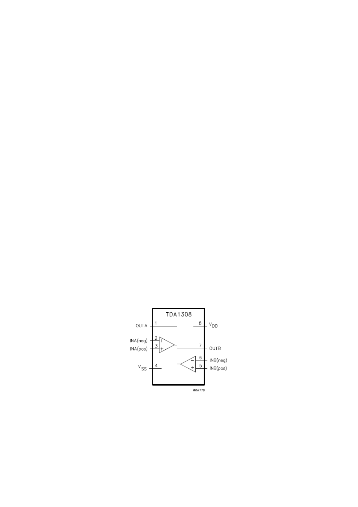
10.10. TDA1308........................................................................................................................ 30
10.10.1. General Description................................................................................................. 30
10.10.2 Features .................................................................................................................... 30
10.10.3. Pinning .................................................................................................................... 30
10.11. TDA1905........................................................................................................................ 31
10.11.1. General Description................................................................................................. 31
10.11.2. Absolute Maximum Ratings.................................................................................... 31
10.11.3. Electrical Characteristics......................................................................................... 32
10.11.4. Muting Function...................................................................................................... 33
10.SERVICE MENU SETTINGS................................................................................................. 34
11.Exploded Diagram.................................................................................................................... 37
12.BLOCK DIAGRAM................................................................................................................ 38
Motherboard Block Diagram.............................................................................................. 38
12.1.
12.2. Power Management
12.3.1. DRX (IF Demodulator), MSP & Video Processor Block Diagram........................... 40
12.3.2. MSP Block Diagram................................................................................................... 41
13.Schematic Diagrams ................................................................................................................. 42
14.PWB Main Board....................................................................................................................... 48
Block Diagram.................................................................................. 39
2
Page 4
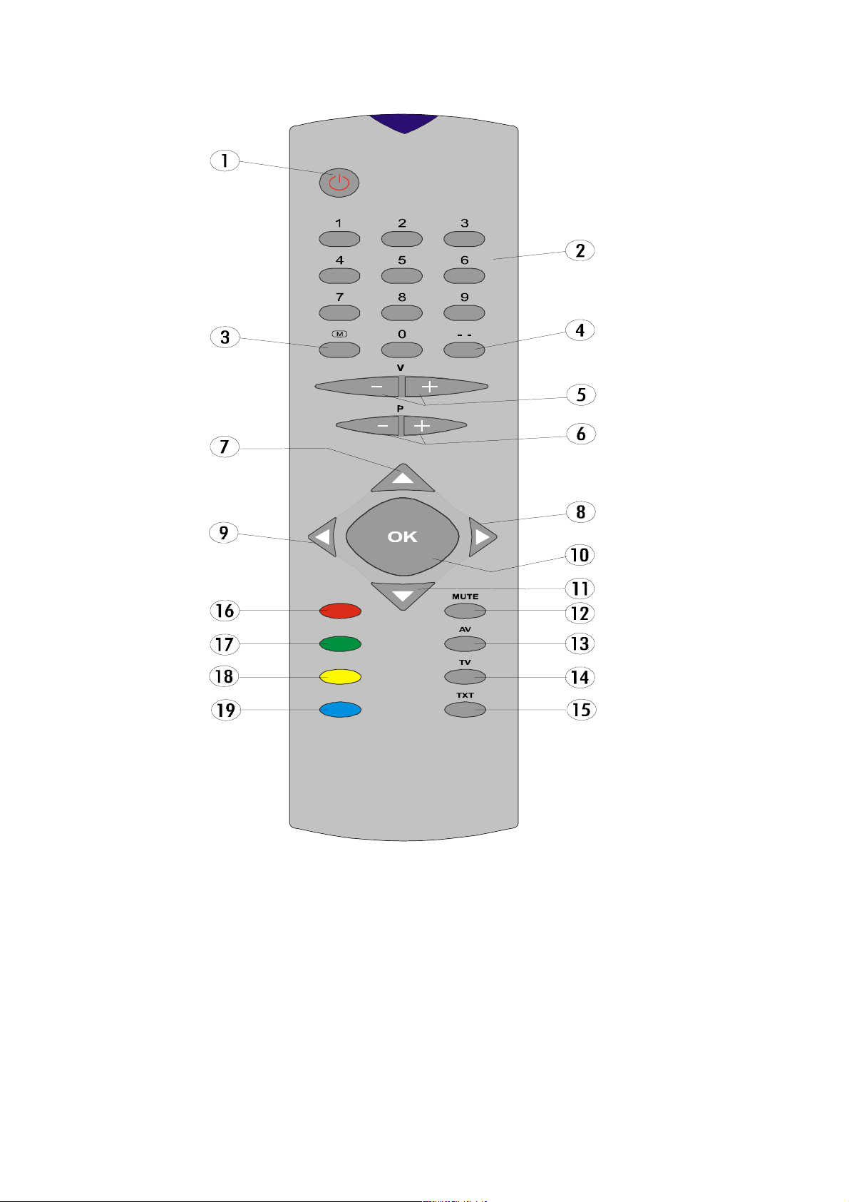
Stand By
0 - 9 Direct Programme
Menu
Cursor Up
Cursor Left
Sound
Picture Menu
Feature Menu
Installation Menu
Double Digit
Volume +/ -
Programme +/ -
Cursor Right
OK
Cursor Down
Mute
External Source
(TV, EXT1, EXT2, EXT3, SVHS, PC)
TV / Quit Menu
Teletext
3
Page 5

1. INTRODUCTION
17MB24 Main Board consists of two major blocks. The first block is analog front-end
and this block is handled by VCTI chip that is highly multifunctional. This IC does
demodulation of Video & Audio from Tuner IF, CVBS, Audio, RGB, SVHS input
selection and processing. It has an audio processor that supports equalizer or tone
control, volume control, AVL, surround effect etc and supplies amplifier, headphone and
CVBS & audio line outputs. It handles video processing such as colour standard
detection and demodulation, picture alignment (brightness, contrast, colour etc.). The IC
also does teletext decoding with fastext memory. After video processing, the processed
video is applied to MST5*7a-M chip in RGB format.
The TV Tuner is an asymmetrical or a symmetrical IF output type and is PLL controlled.
The IF signal is applied single saw filter. After the SAW filter block, IF signal is applied to
VCTI IF inputs (Pin 16 and 17).
As VCTI can handle all the audio processing, there is no need for additional audio
processor solution on the board. VCTI supports three Audio outputs. These outputs are
assigned to Headphone, Speaker and I2C Controlled audio switch. The board employs
TDA1905 and TDA1308 to drive speaker and headphone outputs respectively.
The Back End section is handled by MST chip. The RGB input can handle standard
interlaced RGB output from VCTI, PC VGA RGB input and YPbPr. There are two set of
ADC is present in MST so YPbPr and VGA sources should be multiplexed.
MST chip have an integrated LVDS transmitter and this LVDS transmitter can be
activated or deactivated by registers so output of MST chip can be LVDS or TTL format.
Backlight is controlled via MST chip there are two pins to control inverter one of them is
used for adjusting backlight the other one is used for backlight on/off control.
2. TUNER
As the thickness of the TV set has a limit, a horizontal mounted tuner is used in the
product, which is suitable for CCIR systems B/G, H, L/ L’, I/I’, and D/K. The tuning is
available through the digitally controlled I2C bus (PLL). Below you will find info on the
Tuner in use.
General description of UV1316:
The UV1316 tuner belongs to the UV 1300 family of tuners, which are designed to meet
a wide range of applications. It is a combined VHF, UHF tuner suitable for CCIR
systems B/G, H, L, L’, I and I’. The low IF output impedance has been designed for
direct drive of a wide variety of SAW filters with sufficient suppression of triple transient.
Features of UV1316:
1. Member of the UV1300 family small sized UHF/VHF tuners
2. Systems CCIR: B/G, H, L, L’, I and I’; OIRT: D/K
3. Digitally controlled (PLL) tuning via I2C-bus
4. Off-air channels, S-cable channels and Hyper band
5. Compact size
6. Complies to “CENELEC EN55020” and “EN55013”
4
Page 6
Pinning:
1. Gain control voltage (AGC) : 4.0V, Max: 4.5V
2. Tuning voltage
3. I²C-bus address select : Max: 5.5V
4. I²C-bus serial clock : Min:-0.3V, Max: 5.5V
5. I²C-bus serial data : Min:-0.3V, Max: 5.5V
6. Not connected
7. PLL supply voltage : 5.0V, Min: 4.75V, Max: 5.5V
8. ADC input
9. Tuner supply voltage : 33V, Min: 30V, Max: 35V
10. Symmetrical IF output 1
11. Symmetrical IF output 2
3. AUDIO AMPLIFIER STAGE WITH TDA1905
The TDA1905 is a monolithic integrated circuit in POWERDIP package, intended for use
as low frequency power amplifier in a wide range of applications in radio and TV sets.
Stereo audio output power (2x3.5W – 16 Ohm at %10 THD), equalizer, FM radio, linear
stereo, German-NICAM stereo, 5-Band equalizer control are supported.
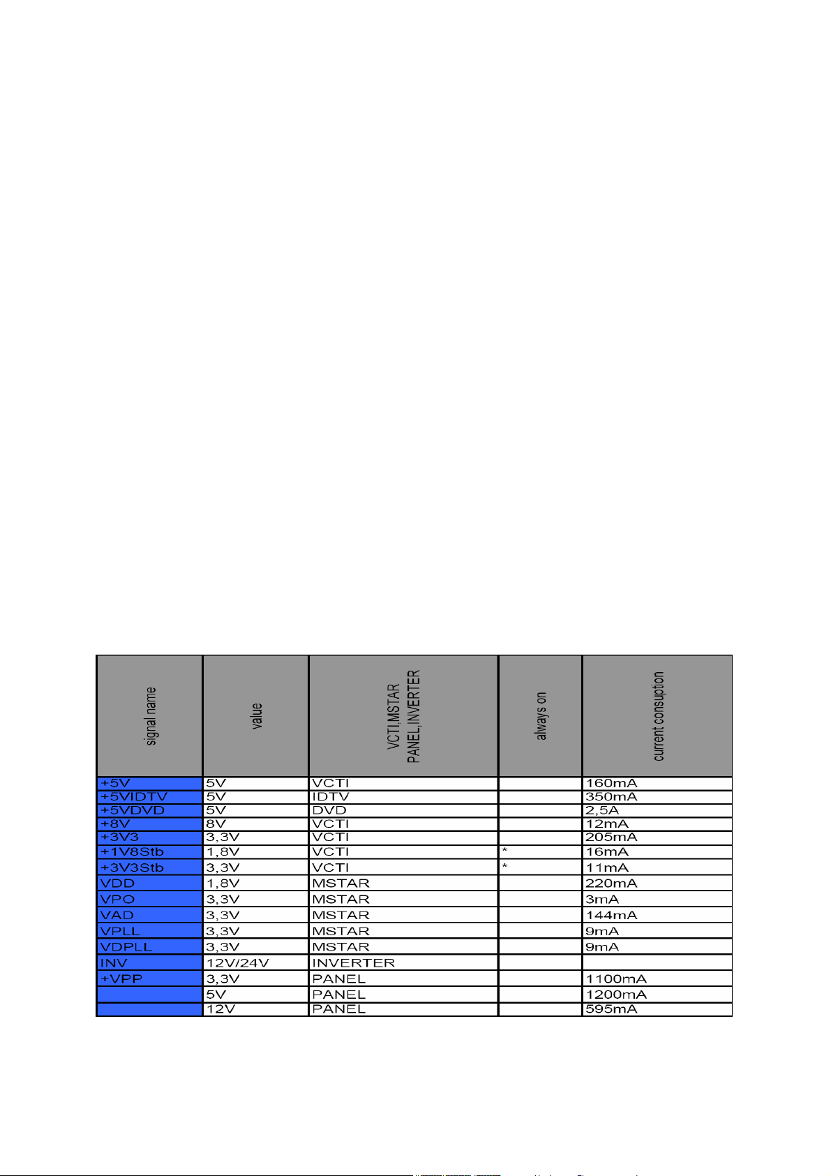
4. POWER STAGE
The DC voltages required at various parts of the chassis and inverters are provided by a
main power supply unit and power interface board. The main power supply unit is
designed for 24V and 12V DC supply. Power stage which is on-chasis generates +12V
for audio amplifier, 1.8V and 3.3V stand by voltage and 8V, 12V, 5V and 3.3Vsupplies
for other different parts of the chassis.
5
Page 7

5. MICROCONTROLLER (VCTI)
General Features
The VCT 49xyI, VCT 48xyI is an IC family of high-quality single-chip TV processors.
Modular design and deep-submicron technology allow the economic integration of
features in all classes of single-scan TV sets. The VCT 49xyI, VCT 48xyI family is based
on functional blocks contained and approved in existing products like DRX 396xA, MSP
34x5G, VSP 94x7B, DDP 3315C, and SDA 55xx. Each member of the family contains
the entire IF, audio, video, display, and deflection processing for 4:3 and 16:9 50/60-Hz
mono and stereo TV sets. The integrated microcontroller is supported by a powerful
OSD generator with integrated Teletext & CC acquisition including on-chip page
memory.
– Submicron CMOS technology
– Low-power standby mode
– Single 20.25 MHz reference crystal
– 8-bit 8051 instruction set compatible CPU
– Up to 256 kB on-chip program ROM
– WST, PDC, VPS, and WSS acquisition
– Up to 10 pages on-chip teletext memory
– Multi-standard QSS IF processing with single SAW
– FM Radio and RDS with standard TV tuner
– TV-sound demodulation:
• all A2 standards
• all NICAM standards
• BTSC/SAP with MNR (DBX optional)
• EIA-J
– Baseband sound processing for loudspeaker channel:
• volume and balance
• bass/treble or equalizer
• loudness and spatial effect (e.g. pseudo stereo)
• Micronas AROUND (virtual Dolby optional)
• Micronas BASS and Subwoofer output
• further optional and licence requiring sound enhancements as BBE, SRS Wow
– CVBS, S-VHS, YCbCr and RGB inputs
– ITU656 input
– 4H adaptive comb filter (PAL/NTSC)
– multi-standard color decoder (PAL/NTSC/SECAM)
– Macrovision Detection
– Nonlinear horizontal scaling “panorama vision”
– Luma and chroma transient improvement (LTI, CTI)
– Non-linear color space enhancement (NCE)
– Dynamic black level expander (BLE)
– Selective Color Enhancer (SCE)
– 8/10 bit ITU656 output
– Soft start/stop of H-drive
6
Page 8

DRX Features
The DRX - Analog TV IF- Demodulator performs the entire multistandard Quasi Split
Sound (QSS) TV IF processing, AGC, video demodulation, and generation of the
second sound IF (SIF) requiring only one SAW filter. The alignment-free DRX does not
need special external components. All control functions and status registers are
accessible via I2C bus interface. Therefore, it simplifies the design of high-quality, highly
standardized IF stages.
– Multistandard QSS IF processing with a single SAW
– Highly reduced amount of external components (no tank circuit, no potentiometers, no
SAW switching)
– Programmable IF frequency (38.9 MHz, 45.75 MHz, 32.9 MHz, 58.75 MHz, 36.125
MHz)
– Digital IF processing for the following standards:
B/G, D/K, I, L/L’, and M/N
– Standard specific digital post filtering
– Standard specific digital video/audio splitting
– Standard specific digital picture carrier recovery:
• alignment-free
• quartz-stable and accurate
• stable frequency lock at 100% modulation and overmodulation up to 150%
• quartz-accurate AFC information
– Programmable standard specific digital group delay equalization
– Automatically frequency-adjusted Nyquist slope, therefore optimal picture and sound
performance over complete lock in frequency range
– Standard-specific digital AGC and delayed tuner AGC with programmable tuner Take
Over Point
Multistandard Sound Processor (MSP) Features
The MSP receives the digital Sound IF signal from the DRX part. The MSP is able to
demodulate all TV sound standards worldwide including the digital NICAM system.
Depending on the VCTI version, the following demodulation modes can be performed.
TV stereo sound standards that are unavailable for a specific VCTI version are
processed in analog mono sound of the standard. In that case, stereo or bilingual
processing will not be possible.
– Sound demodulator and stereo decoder
– Audio processing for loudspeaker channels:
• volume
• Automatic Volume Correction (AVC)
• bass/treble or equalizer
• loudness
• balance
• configurable Subwoofer output
– Optional features for loudspeaker channels:
• Virtual Dolby Surround (VDS)
• SRS WOW
• BBE High Definition Sound
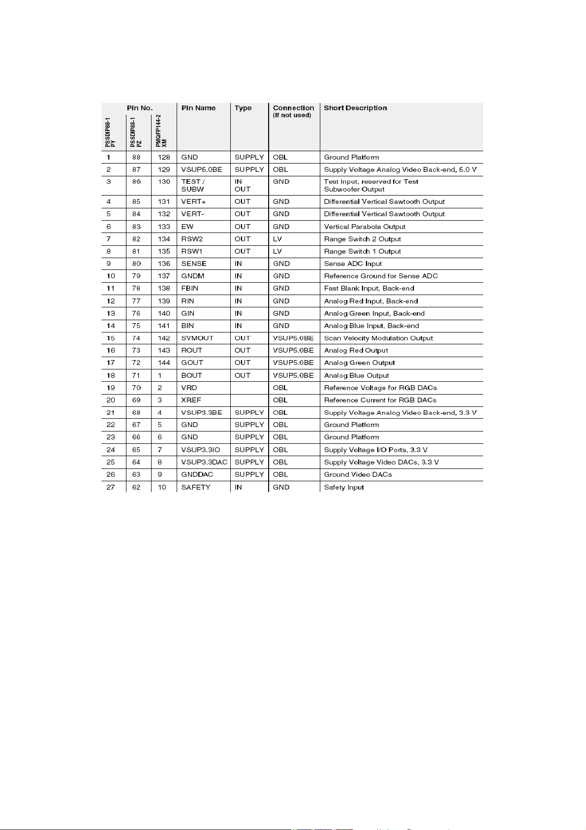
– PMQFP144-2 package:
7
Page 9

• 6 analog audio inputs
• 4 analog audio outputs
– PSSDIP88-1 package:
• 4 analog audio inputs
• 2 analog audio outputs
• 2 configurable analog audio inputs/outputs
Video Features
The TVT is a Teletext decoder for decoding World System Teletext data, as well as
Video Programming System (VPS), Program Delivery Control (PDC), and Wide-Screen
Signalling (WSS) data used for PALplus transmissions (line 23). The device also
supports Closed Caption acquisition and decoding. The TVT provides an integrated
general-purpose, fully 8051-compatible microcontroller with television-specific hardware
features. The microcontroller has been enhanced to provide powerful features such as
memory banking, data pointer, additional interrupts, etc. The on-chip display unit for
displaying Level 1.5 Teletext data can also be used for customer-defined onscreen
displays.
The TVT has an internal XRAM of 20 KB and an internal ROM of up to 256 KB.
ROMless versions can address up to 1 MB of external RAM and ROM. The 8-bit
microcontroller runs at 296 ns cycle time. The controller with dedicated hardware does
most of the internal TTX acquisition processing, transfers data to/from external memory
interface, and receives/transmits data via I2C-bus interface. In combination with
dedicated hardware, the slicer stores TTX data in a VBI buffer of 1 KB. The
microcontroller firmware performs all the acquisition tasks (hamming and parity checks,
page search, and evaluation of header control bits) once per field. Additionally, the
firmware can provide high-end Teletext features like Packet-26 handling, FLOF/TOP
and list-pages. The interface-to-user software is optimized for minimal overhead. TVT is
realized in deep submicron technology with 1.8 V supply voltage and 3.3 V I/O (TTL
compatible).
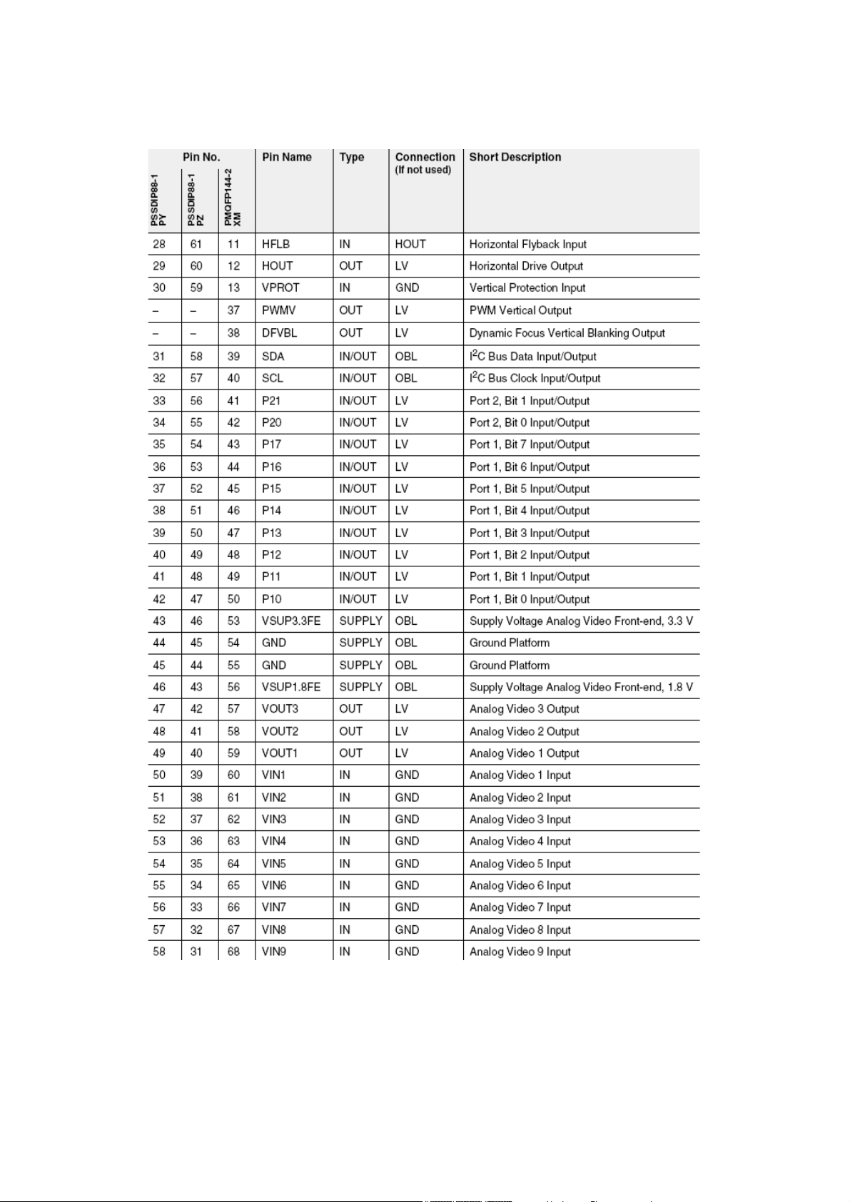
– 11 analog video inputs (CVBS/Y/C/RGB/YCbCr)
– 3 analog video outputs
– integrated Y+C adder
– integrated high-quality A/D converters and associated clamp and AGC circuits
– high-performance 4H comb filter (PAL/NTSC) with vertical peaking
– multistandard color decoder PAL/NTSC/SECAM including all substandards
– macrovision-compliant multistandard sync processing
– macrovision detection
– RGB/YCbCr component processing and associated contrast, color saturation and tint
circuits
– high-quality soft mixer controlled by fast blank (alpha blending)
– fast blank monitor via I2C
– ITU656 input
– linear horizontal scaling (0.25 to 4)
– nonlinear horizontal scaling “panorama vision”
– split screen (OSD and video side by side)
– letter box detector (auto-wide)
– noise measurement
8
Page 10

Controller Features
The TVT is a Teletext decoder for decoding World System Teletext data, as well as
Video Programming System (VPS), Program Delivery Control (PDC), and Wide-Screen
Signalling (WSS) data used for PALplus transmissions (line 23). The device also
supports Closed Caption acquisition and decoding. The TVT provides an integrated
general-purpose, fully 8051-compatible microcontroller with television-specific hardware
features. The microcontroller has been enhanced to provide powerful features such as
memory banking, data pointer, additional interrupts, etc.
– Single external 20.25 MHz crystal, all necessary clocks are generated internally
– Normal mode: 40.5 MHz CPU clock, Power Save mode: 10.125 MHz
– Up to 256 KB on-chip program ROM
– 256 byte on-chip program RAM
– 128 byte on-chip extended stack RAM
– 20 kilobyte on-chip extended data RAM (XRAM)
– Memory banking up to 1 MB
– Non-multiplexed 8-bit data and 20-bit address bus
– Eight 16-bit data pointer registers (DPTR)
– 4-level, 24-input interrupt controller
– Patch module for 16 ROM locations
– Two 16-bit reloadable timers
– Capture-compare timer for infrared decoding
– Watchdog timer
– UART
– Real time clock (RTC)
– PWM units (2 channels 14-bit, 6 channels 8-bit)
– 8-bit ADC (4 channels)
– I2C bus master/slave interface
– Up to 24 programmable I/O ports
– Flash version for PMQFP144 and PSSDIP88 packages (SST39LF020 or compatible)
– ROM-less version with 1 MB address space for external program and data memory
OSD & Teletext Features
The on-chip display unit for displaying Level 1.5 Teletext data can also be used for
customer-defined onscreen displays. The TVT has an internal XRAM of 20 KB and an
internal ROM of up to 256 KB. ROMless versions can address up to 1 MB of external
RAM and ROM.
In combination with dedicated hardware, the slicer stores TTX data in a VBI buffer of 1
KB. The microcontroller firmware performs all the acquisition tasks (hamming and parity
checks, page search, and evaluation of header control bits) once per field. Additionally,
the firmware can provide high-end Teletext features like Packet-26 handling, FLOF/TOP
and list-pages. The interface-to-user software is optimized for minimal overhead.
Port Allocation
9
Page 11
10 11
Page 12
Page 13
12
Page 14

6. SCALER & DEINTERLACER (MST)
The MST5*7 is total solution graphics processing IC for LCD displays with panel
resolutions up to WXGA+/SXGA+. It is configured with a high-speed integrated tripleADC/PLL, a high quality display processing engine, and an integrated multi-purpose
output display interface that can support all major panel interface formats. To further
reduce system costs, the MST5*7 also integrates intelligent power management control
capability for green-mode requirements and spread-spectrum support for EMI
management.
General Features
- Two RGB analog input ports support up to 165 MHz (UXGA @ 60Hz)
- Full SOG and composite sync support, including copy protected signals
Display Features
- Patent-pending Hybrid Image Resolution Converter
- Variable sharpness control
- Interlaced to progressive conversion
- Patent-pending Dynamic Frame-Rate generator (DFR) – short line storage frame
extension technique eliminates short lines in output frames
- Media Window Enhancement (MWE)
- Peaking and coring functions for sharpness enhancement and noise reduction
- Brightness and contrast control
- Programmable 10-bit gamma correction
- sRGB support
Auto Detection Features
- Auto input signal format (SOG, composite, separated HSYNC, and VSYNC)
- Input mode detection support analyzes input video signal (H/V polarity, H/V frequency,
interlace/field detect) – extensive status registers support robust detection of all VESA
and IBM modes
- Auto-tuning function including support for phase selection, image position, offset &
gain and jitter detection
- Smart screen-fitting
OSD Features
- Built-in OSD generator with 291 character font programmable RAM
13
Page 15
- Internal OSD rotation degree of 90 and 270
- Supports 2/4/8 multi-color fonts
- Supports 8/16/256 color palette
- Supports 1K code attributes
- Gradient color function
- Hardware button animation function
- Pattern generator for production test
- Supports OSD MUX and alpha blending
capability
7. SERIAL 32K I2C EEPROM 24LC32
24LC32A is a 32 Kbit Electrically Erasable PROM. The device is organized as four
blocks of 8K x 8-bit memory with a 2-wire serial interface. Low-voltage design permits
operation down to 1.8V, with standby and active currents of only 1 μA and 1 mA,
respectively. It has been developed for advanced, lowpower applications such as
personal communications or data acquisition. The 24XX32A also has a page write
capability for up to 32 bytes of data. Functional address lines allow up to eight devices
on the same bus, for up to 256 Kbits address space. The 24XX32A is available in the
standard 8-pin (Vcc, WP, SDA (i2c data), SCL (i2c clock), GNDx4). WP pin is critcal pin.
If WP is high, writing is not possible to EEPROM. If WP is low, writing is possible to
EEPROM.
8. CLASS AB STEREO HEADPHONE DRIVER TDA1308
The TDA1308 is an integrated class AB stereo headphone driver. The device is
fabricated in a 1 mm CMOS process and has been primarily developed for portable
digital audio applications.
9. SAW FILTER
X6966D Standard:
• B/G
• D/K
• I
14
Page 16

• L/L’
Features:
• IF filter for digital cable TV
• Standard IC package
Pin configuration:
1 Input
2 Input - ground
3 Chip carrier - ground
4 Output
5 Output
Frequency response:
15
Page 17

10. IC DESCRIPTIONS AND INTERNAL BLOCK DIAGRAM
LM1117
LM1086
LM317
MP1593
IRF7314
FDC642P
74HCT4053
TEA6420
PI5V330
TDA1308
TDA1905
10.1. LM1117
10.1.1. General Description
The LM1117 is a series of low dropout voltage regulators with a dropout of 1.2V at
800mA of load current. It has the same pin-out as National Semiconductor’s industry
standard LM317. The LM1117 is available in an adjustable version, which can set the
output voltage from 1.25V to 13.8V with only two external resistors. In addition, it is also
available in five fixed voltages, 1.8V, 2.5V, 2.85V, 3.3V, and 5V. The LM1117 offers
current limiting and thermal shutdown. Its circuit includes a zener trimmed bandgap
reference to as-sure output voltage accuracy to within ±1%. The LM1117 series is
available in SOT- 223, TO-220, and TO-252 D-PAK packages. A minimum of 10μF
tantalum capacitor is required at the output to improve the transient response and
stability.
10.1.2. Features
• Available in 1.8V, 2.5V, 2.85V, 3.3V, 5V, and Adjustable Versions
• Space Saving SOT-223 Package
16
Page 18

• Current Limiting and Thermal Protection
• Output Current 800mA
• Line Regulation 0.2% (Max)
• Load Regulation 0.4% (Max)
• Temperature Range
— LM1117 0°C to 125°C
— LM1117I -40°C to 125°C
10.1.3. Applications
• 2.85V Model for SCSI-2 Active Termination
• Post Regulator for Switching DC/DC Converter
• High Efficiency Linear Regulators
• Battery Charger
• Battery Powered Instrumentation
10.1.4. Absolute Maximum Ratings
10.1.5. Connection Diagrams
10.2. LM1086
10.2.1. General Description
The LM1086 is a low dropout three terminal regulator with 1.5A output current capability.
The output voltage is adjustable with the use of a resistor divider. Dropout is guaranteed
at a maximum of 500 mV at maximum output current. It's low dropout voltage and fast
transient response make it ideal for low voltage microprocessor applications. Internal
current and thermal limiting provides protection against any overload condition
that would create excessive junction temperature.
10.2.2. Features
● Low Dropout Voltage 500mV at 1.5A Output Current
17
Page 19

● Fast Transient Response
● 0.015% Line Regulation
● 0.1% Load Regulation
● Internal Thermal and Current Limiting
● Adjustable or Fixed Output Voltage(1.5, 2.5, 2.85, 3.0, 3.3, 5.0V)
● Surface Mount Package SOT-223 & TO-263 (D2 Package)
● 100% Thermal Limit Burn-in
10.2.3. Applications
● Battery Charger
Adjustable Power Supplies
●
Constant Current Regulators
●
Portable Instrumentation
●
High Efficiency Linear Power Supplies
●
High Efficiency "Green" Computer Systems
●
SMPS Post-Regulator
●
Power PC Supplies
●
Powering VGA & Sound Card
●
10.2.4. Absolute Maximum Ratings
18
Page 20

10.2.5. Connection Diagrams
10.3. LM317
10.3.1. General Description
The LM117/LM217/LM317 are monolithic integrated circuit in TO-220, ISOWATT220,
TO-packages intended for use as positive adjustable voltage regulators. They are
designed to supply more than 1.5A of load current with an output voltage adjustable
1.2 to 37V range. The nominal output voltage is selected by means of only a resistive
divider, making exceptionally easy to use and eliminating the stocking of many fixed
regulators.
10.3.2. Features
● Output voltage range: 1.2 to 37V
● Output current in excess of 1.5A
● 0.1% Line and Load Regulation
● Floating Operation for High Voltages
● Complete Series of Protections: Current Limiting, Thermal Shutdown and SOA Control
19
Page 21

10.3.3. Connection Diagrams
10.4. MP1593
10.4.1. General Description
The MP1593 is a step-down regulator with an internal Power MOSFET. It achieves 3A
continuous output current over a wide input supply range with excellent load and line
regulation. Current mode operation provides fast transient response and eases loop
stabilization. Fault condition protection includes cycle-by-cycle current limiting and
thermal shutdown. Adjustable soft-start reduces the stress on the input source at turnon. In shutdown mode the regulator draws 20μA of supply current. The MP1593
requires a minimum number of readily available external components to complete a 3A
step down DC to DC converter solution.
10.4.2. Features
● 3A Output Current
● Programmable Soft-Start
● 100mΩ Internal Power MOSFET Switch
● Stable with Low ESR Output Ceramic Capacitors
● Up to 95% Efficiency
● 20μA Shutdown Mode
● Fixed 385KHz Frequency
● Thermal Shutdown
● Cycle-by-Cycle Over Current Protection
● Wide 4.75 to 28V Operating Input Range
● Output Adjustable from 1.22V
● Under Voltage Lockout
● Available in 8-Pin SOIC Package
10.4.3. Applications
● Distributed Power Systems
● Battery Chargers
● Pre-Regulator for Linear Regulators
● Flat Panel TVs
● Set-Top Boxes
● Cigarette Lighter Powered Devices
● DVD/PVR Devices
20
Page 22

10.4.4. Absolute Maximum Ratings
10.4.5. Electrical Characteristics
10.4.6. Pin Functions
Pin1:BS
High-Side Gate Drive Boost Input. BS supplies the drive for the high-side N-Channel
MOSFET switch. Connect a 10nF or greater capacitor from SW to BS to power the high
side switch.
Pin2:IN
Power Input. IN supplies the power to the IC, as well as the step-down converter
switches. Drive IN with a 4.75V to 28V power source. Bypass IN to GND with a suitably
large capacitor to eliminate noise on the input to the IC.
Pin3:SW
21
Page 23

Power Switching Output. SW is the switching node that supplies power to the output.
Connect the output LC filter from SW to the output load. Note that a capacitor is required
from SW to BS to power the high-side switch
Pin4:GND
Ground.
Pin5:FB
Feedback Input. FB senses the output voltage to regulate that voltage. Drive FB with a
resistive voltage divider from the output voltage. The feedback threshold is 1.222V.
Pin6:COMP
Compensation Node. COMP is used to compensate the regulation control loop. Connect
a series RC network from COMP to GND to compensate the regulation control loop. In
some cases, an additional capacitor from COMP to GND is required.
Pin7:EN
Enable Input. EN is a digital input that turns the regulator on or off. Drive EN high to turn
on the regulator, drive EN low to turn it off. An Under Voltage Lockout (UVLO) function
can be implemented by the addition of a resistor divider from VIN to GND. For complete
low current shutdown its needs to be less than 0.7V. For automatic startup, leave EN
unconnected.
Pin8:SS
Soft-Start Control Input. SS controls the soft-start period. Connect a capacitor from SS
to GND to set the soft-start period. A 0.1μF capacitor sets the soft-start period to 10ms.
To disable the soft-start feature, leave SS unconnected.
.
10.5. IRF7314-IRF7316
Fifth Generation HEXFETs from International Rectifier utilize advanced processing
techniques to achieve extremely low on-resistance per silicon area. This benefit,
combined with the fast switching speed and ruggedized device design that HEXFET
Power MOSFETs are well known for, provides the designer with an extremely efficient
and reliable device for use in a wide variety of applications. The SO-8 has been
modified through a customized leadframe for enhanced thermal characteristics and
multiple-die capability making it ideal in a variety of power applications. With these
improvements, multiple devices can be used in an application with dramatically reduced
board space. The package is designed for vapor phase, infra red, or wave soldering
techniques.
10.5.1. Absolute Maximum Ratings
7314 (TA = 25°C Unless Otherwise Noted)
22
Page 24

7316 (
TA = 25°C Unless Otherwise Noted)
10.6. FDC642P
10.6.1. General Description
This p-channel 2.5V specified MOSFET is produced using Fairchild’s advanced
PowerTrench process that has been especially tailored to minimize on state resistance
and yet maintain low gate charge for superior switching performance.
10.6.2 . Features
23
Page 25

10.6.3. Absolute Maximum Ratings
10.6.4. Connection Diagram
10.7. 74HCT4053
10.7.1. General Description
The 74HC/HCT4053 are high-speed Si-gate CMOS devices and are pin compatible with
the “4053” of the “4000B” series. They are specified in compliance with JEDEC standard
no. 7A.
The 74HC/HCT4053 are triple 2-channel analog multiplexers/demultiplexers with a
common enable input (E). Each multiplexer/demultiplexer has two independent
inputs/outputs (nY0 and nY1), a common input/output (nZ) and three digital select inputs
(S1 to S3).
With E LOW, one of the two switches is selected (low impedance ON-state) by S1 to S3.
With E HIGH, all switches are in the high impedance OFF-state, independent of S1 to
S3.
VCC and GND are the supply voltage pins for the digital control inputs (S1, to S3, and
E). The VCC to GND ranges are 2.0 to 10.0 V for HC and 4.5 to 5.5 V for HCT. The
analog inputs/outputs (nY0 and nY1, and nZ) can swing between VCC as a positive limit
and VEE as a negative limit. VCC - VEE may not exceed 10.0 V.
For operation as a digital multiplexer/demultiplexer, VEE is connected to GND (typically
ground).
10.7.2. Features
●Low “ON” resistance:
24
Page 26

80 W (typ.) at VCC - VEE = 4.5 V
70 W (typ.) at VCC - VEE = 6.0 V
60 W (typ.) at VCC - VEE = 9.0 V
● Logic level translation:to enable 5 V logic to communicate with ± 5 V analog signals
● Typical “break before make” built in
● Output capability: non-standard
● ICC category: MSI
10.7.3. Application
● Analog multiplexing and demultiplexing
● Digital multiplexing and demultiplexing
● Signal gating
10.7.4. Absolute Maximum Ratings
10.7.5. Connection Diagram
25
Page 27

26
Page 28

10.8.TEA6420
10.8.1 General Description
The TEA6420 switches 5 stereo audio inputs on 4 stereo outputs. All the switching
possibilities are changed through the I2C bus.
10.8.2. Features
● 5 Stereo Inputs
● 4 Stereo Outputs Gain Control 0/2/4/6dB/ Mute for Each Output
● Cascadable (2 different addresses)
● Serial Bus Controlled
● Very Low Noise & Very Low Distortion
10.8.3. Absolute Maximum Ratings
10.8.4. Electrical Characteristics
27
Page 29

10.8.5. Block Diagram
10.8.6. Connection Diagram
28
Page 30

10.9. PI5V330
10.9.1. General Description
The PI5V330 is well suited for video applications when switching composite or RGB
analog. A picturein- picture application will be described in this brief. The pixel-rate
creates video overlays so two or more pictures can be viewed at the same time. An
inexpensive NTSC titler can be implemented by superimposing the output of a character
generator on a standard composite video background.
10.9.2. Features
• High-performance solution to switch between video sources
• Wide bandwidth: 200 MHz
• Low On-Resistance: 3Ω
• Low crosstalk at 10 MHz: –58dB
• Ultra-low quiescent power (0.1μA typical)
• Single supply operation: +5.0V
• Fast switching: 10ns
• High-current output: 100mA
10.9.3. Absolute Maximum Ratings
10.9.4. Connection Diagram
29
Page 31

10.10. TDA1308
10.10.1. General Description
The TDA1308 is an integrated class AB stereo headphone driver contained in an SO8
or a DIP8 plastic package. The device is fabricated in a 1 mm CMOS process and has
been primarily developed for portable digital audio applications. It gets its input from two
analog audio outputs (DACA_L and DACA_R) of MSP 34x0G. The gain of the output is
adjustable by the feedback resistor between the inputs and outputs.
10.10.2 Features
● Wide temperature range
● No switch ON/OFF clicks
● Excellent power supply ripple rejection
● Low power consumption
● Short-circuit resistant
● High performance
● High signal-to-noise ratio
● High slew rate
● Low distortion
● Large output voltage swing.
10.10.3. Pinning
OUTA
INA(neg)
INA(pos)
V
SS
TDA1308
1
2
3
4
8
7
6
5
MKA779
V
DD
OUTB
INB(neg)
INB(pos)
30
Page 32

10.11. TDA1905
10.11.1. General Description
The TDA1905 is a monolithic integrated circuit in POWERDIP package, intended for use
as low frequency power amplifier in a wide range of applications in radio and TV sets:
– muting facility
– protection against chip over temperature
– very low noise
– high supply voltage rejection
– low “switch-on” noise
– voltage range 4V to 30V
The TDA 1905 is assembled in a new plastic package, the POWERDIP, that offers the
same assembly ease, space and cost saving of a normal dual in-line package but with
a power dissipation of upto 6W and a thermal resistance of 15°C/W (junction to pins).
10.11.2. Absolute Maximum Ratings
31
Page 33

10.11.3. Electrical Characteristics
32
Page 34

10.11.4. Muting Function
33
Page 35

10.SERVICE MENU SETTINGS
Remote control code for opening the SERVICE MENU: MENU 4725
1. First APS <Yes/No>
2. BURN_IN_MODE <Yes/No>
3. FACTORY MENU
3.1.1. Language
<English, Deutsch, Francais, Spanish, Portuguese, Italiano, Svenska,
Dansk, Türkçe, Hungarian, Czech, Polish or Croatian>
3.1.2. Country
<Germany, Denmark, Spain, France, Finland, Great Britain, Greece,
Hungary, Italy, Norway, Netherlands, Portugal, Poland, Swenden,
Slovenia, Slovakia,Turkey, Others, Japan, Korea, America, Austria,
Belgium, Switzerland, Czech Rep.>
3.1.3. Volume <0..63>
3.1.4. HP Volume <0..63>
3.1.5. Teletext Region
< East Europe, West Europe, Cyrillic, Turkish/Greek, Arabic/Hebrew >
3.1.6. Menu Colour <Opaque, Transparent>
3.1.7. Picture Mode
3.1.7.1.1.1. Brightness (Bright) <0..63>
3.1.7.1.1.2. Contrast (Bright) <0..63>
3.1.7.1.1.3. Colour (Bright) <0..63>
3.1.7.1.1.4. Brightness (Standard) <0..63>
3.1.7.1.1.5. Contrast (Standard) <0..63>
3.1.7.1.1.6. Clour (Standard) <0..63>
3.1.7.1.1.7. Brightness (Soft) <0..63>
3.1.7.1.1.8. Contrast (Soft) <0..63>
3.1.7.1.1.9. Colour (Soft) <0..63>
4. VCTI DAC Adjust.
4.1.1. Cutoff Red <0..512>
4.1.2. Cutoff Green <0..512>
4.1.3. Cutoff Blue <0..512>
4.1.4. Whitedrv. Red <0..512>
4.1.5. Whitedrv. Green <0..512>
4.1.6. Whitedrv. Blue <0..512>
34
Page 36

4.1.7. PAL CVBS Brigh <0..63>
4.1.8. PAL RGB Brigh <0..63>
4.1.9. NTSC CVBS Brigh <0..63>
4.1.10. NTSC RGB Brigh <0..63>
4.1.11. PAL CVBS Color <0..63>
4.1.12. PAL RGB Color <0..63>
4.1.13. NTSC CVBS Color <0..63>
4.1.14. NTSC RGB Color <0..63>
5. Txt & FE OSD Settings
5.1.1. Txt&FE OSD H-Shift <0..256>
5.1.2. Txt&FE OSD V-Shift <0..256>
5.1.3. Txt H-Shift Split Screen <0..256>
5.1.4. Txt&FE OSD Pixel Clock <0..256>
5.1.5. YDELAY PAL <0..256>
5.1.6. YDELAY NTSC <0..256>
6. Options1
6.1.1. IDTV <Yes, No>
6.1.2. SVHS-EXT2 <Yes, No>
6.1.3. FRONT-AV <Yes, No>
6.1.4. SVHS <Yes, No>
6.1.5. PC <Yes, No>
6.1.6. YPBPR <Yes, No>
6.1.7. HP ITEM ON MENU <Yes, No>
6.1.8. BLUE SCREEN <Yes, No>
6.1.9. SEARCH FOR BG, DK, I <Yes, No>
6.1.10. SERAC FOR L/L’ <Yes, No>
6.1.11. Pref. Search Standard <BG-DK-I, L-L’, M>
6.1.12. Station Ident <Yes, No>
6.1.13. POWER ON TO STANDBY <Yes, No>
7. Options2
7.1.1. Tuner Options
7.1.1.1.1. Control Byte <128..256>
7.1.1.1.2. BSW1 <0..256>
7.1.1.1.3. BSW2 <0..256>
7.1.1.1.4. BSW3 <0..256>
7.1.1.1.5. VHF1-3-L <0..256>
7.1.1.1.6. VHF1-3-H <0..256>
7.1.1.1.7. VHF3-UHF_L <0..256>
7.1.1.1.8. VHF3-UHF_H <0..256>
7.1.1.1.9. Top Setting-PAL <0..256>
7.1.1.1.10. Top Setting-SECAM
7.1.2. Blue Back. On Menu <Yes, No>
7.1.3. Dynamic Bass On Menu <Yes, No>
7.1.4. Vir. Dolby On Menu <Yes, No>
7.1.5. APS Delay Time(ms) <0..256>
7.1.6. Video Peaking <0..256>
7.1.7. Comb Filter/CTI/LTI <Yes, No>
8. Audio Options
8.1.1. Equalizer <Yes, No>
<0..256>
35
Page 37

8.1.2. Carrier Mute <Yes, No>
8.1.3. FM Presc_AVL_off <0..256>
8.1.4. NICAM Presc_AVL_off <0..256>
8.1.5. Scart Presc_AVL_off <0..256>
8.1.6. FM Presc_AVL_on <0..256>
8.1.7. NICAM Presc_AVL_on <0..256>
8.1.8. Scart Presc_AVL_on <0..256>
8.1.9. Line-out Via HP <Yes, No>
9. 9-Auto calibration
9.1.1. Exit
9.1.2. AutoColor
9.1.3. AdcGain
R 99 G 99 B 99
9.1.4. ADC Offset
R 133 G 129 B 145
9.1.5. Color temp Cool
9.1.6. Gain
R 140 G 140 B 140
9.1.7. Offset
R 118 G 120 B 127
9.1.8. Con Max 145
9.1.9. Bri Mid 104
9.1.10. Color 32
9.1.11. Sharp 9
10. 10-INIT NVM <Yes/No>
11. 11-SELECTED PANEL <A201SN02_V4, PANEL_5, PANEL_6, PANEL_7,
PANEL_8, PANEL_9, >
17.06.2006Remote Control Type: RC1090, OTHERS, RC1243
36
Page 38

No. 0235
EXPLODED DIAGRAM
37
Page 39

12. BLOCK DIAGRAMS
12.1. General Block Diagram
Note: Dashed lines show basic option (without audio switch)
38
Page 40

12.2. Power Management
39
Page 41

TAGC
SIF
AIN
AOUT
SPEAKER
SUBW
IFIN+
IFIN-
CVBS in
YCbCr in
RGB in
CVBS out
656 in
IF
Frontend
Video
Frontend
Slicer
IF
Processor
Comb
Filter
Component
Bus
Arbiter
Interface
Demodulator
Color
Decoder
Generator
Sound
Display
Panorama
Scaler
Audio
Processor
2
I C Master/
Slave
Display &
Deflection
Processor
Video
Backend
656 out
PROT
HOUT
HFLB
VERT
EW
SVM
RGB out
RGB in
SENSE
RSW
2
IC
24kB
Char ROM
24kB XRAM
256kB
Prog ROM
No. 0235
Timer
CRT
CPU
8051
Memory
Interface
ADB, DB, PSENQ,
PSWEQ, WRQ, RDQ
PWM
ADC
UART
Watchdog
RTC
I/O Ports
Pxy
BLOCK DIAGRAM
Reset & Test
Logic
Clock
Generator
RESETQ
TEST
XTAL1
XTAL2
40
Page 42

41
Page 43

MECH_SW
+12V
R900
22k
+5V/+3V3Stb
16V
100n
PVCC_ON/OFF
C901
C900
IC901
IRF7314
MUTE_INV
1k
R936
50V
100n
C940
8SS
7EN
5FB
2k
R933
R120 will be 15k ohm for 3.3V output.
30k
R934
22u
16V
C939
C941
C134 will be 8.2 nF for 3.3V output.
C944
10n
50V
R935
10k
R130 will be 5.6k ohm for 3.3V output.
22u
16V
C942
IC903
6D4
16V
100u
IC904
1D 1
2D 2 5D3
NTGS3446
3G 4S
C938
R937
+12V
F901
8D1A
16V
7D1
5D2
F902
D900
HER206
+12V_AUD
C949
100u
D901
HER206
16V
C951
100n
A/D_DIM
50V
100n
BKL_ON/OFF
16V
100n
C954
C955
11
10
9
8
7
6
5
4
+12V_INV
C952
100n
50V
C945
10n
Optional NC
50V
7k5
C953
100u
16V
3
2
1
PL902
PL900
BKL_ON/OFF
A/D_DIM
100n
+5V/+3V3Stb
C946
220u
50V
16V
34
56
12
R938
10k
V_DELAY
100n
C959
25V
1N4148
V_GATE
BC858B
Q909
470R
R948
33k
R940
Q907
BC848B
D902
+3V3Stb
10k
R946
3k3
R939
BC858B
Q910
10k
R941
R942
10k
D904
BAW56
+12VStb
+5V/+3V3Stb
+12V_PSU
+12V_PSU +12V_PSU
2k
10k
R945
R947
D905
BZT52C43
+12V_PSU
78
91 0
C943
6D4
+1V8
16V
100u
+5V/+3V3Stb
C947
+3V3
+12V
STBY_ON/OFF
+1V8Stb
+1V8
+3V3Stb
PVCC_ON/OFF
PVCC PVCC
11 12
13 14
15 16
17 18
19 20
PL901
+12V_INV
+12V_PSU
+12VStb
C950
C948
100n
50V
100n
12
34
56
78
91 0
11 12
13 14
15 16
50V
17 18
19 20
+1V8
+3V3Stb
+3V3
+12V_INV
+12V_PSU
MUTE_INV
MECH_SW
+5V
+8V
+12V_AUD
+5V/+3V3Stb
10u
16V
C958
L905
220u
C957
16V
50V
100n
C956
F903
1
2
3
PL903
4
1N4148
5
R943
R944
D903
BC858B
Q908
6
10k
1k
MECH_SW
+12V_PSU
7
10k
R949
+12V_PSU
8
A/D_DIM
9
V_DELAY
BKL_ON/OFF
10
BC848B
Q911
50V
100n
V_GATE
R902
+12V_PSU
C908
100n
50V
R903
10R
22k
R904
10R
Tact Switch Option
S901
IC900
1S 1
2G 1
3S 2 6D2A
4G 2
IRF7314
+12VStb
F900
8D1A
7D1
C924
220u
16V
5D2
C926
100n
50V
L902
C931
100n
50V
+12VStb
C933
R918
1k
BC848B
Q903
100n
R920
22k
R926
R923
10k
22k
R925
10R
22k
R932
STBY_ON/OFF
BC848B
1S 1
2G 1
+12VStb
3S 2 6D2A
R930
10R
4G 2
Q906
IC902
150R 600mA lik ferit
+12VStb
C911
100n
50V
S900
LM1086
IC906
2VOUT3 VIN
LM317
IC905
ADJ
1
47u
16V
+5V/+3V3Stb
Q900
C906
2OUT3I N
R908
GND
22k
C910
1
16V
100n
91R
R905
470R
R906
47R
R907
C912
10u
16V
C907
100n
16V
35V
100u
C904
16V
100n
C903
BC848B
R901
10k
L900
L901
150R 600mA lik ferit
C914
100n
16V
+8V +8V
C913
16V
100n
22k
R910
34
100n
C915
220u
16V
5
2
+3V3Stb
C917
100n
50V
OPTIONAL JUMPER
16V
100u
C916
16V
100n
C918
6
Q901
FDC642P
1
C921
470u
16V
+3V3Stb
C919
16V
PVCC
LM317
IC907
ADJ
47u
1
C922
100n
16V
2OUT3I N
C920
STBY_ON/OFF
IC908
LM1117-DPAK-1.8V
OUT
IN
3
VOUT
GND
1
4
35V
100u
R913
R914
R915
C925
STBY_ON/OFF_INV
220R
680R
1R
100n
R916
2
1k
C929
100n
50V
C928
16V
BC848B
Q902
+5V
C930
100n
16V
+3V3Stb
R917
C935
12k
R919
4k7
22n
50V
C934
1B S
2I N
MP1593-DC/DC
3S W 6COMP
4 GND
SS33
IC909
+1V8Stb
C932
100u
16V
+12VStb
+1V8Stb
68n
3k3
50V
R921
R924
100R
3k3
R922
BC848B
Q904
50V
C936
STBY_ON/OFF_INV
R927
12k
Q905
BC848B
Optional NC
L903
10u
L904
22uH_3.9A_SMD
1D 1
2D 2 5D3
3G 4S
47u
16V
C937
+12VStb
+3V3Stb
68n
3k3
R928
R931
100R
R929
3k3
47u
16V
NTGS3446
No. 0235
POWER DISTRIBUTION
42
Page 44

SC1_R_OUT
SC1_V_OUT
SC1_V_IN
DVD_RXD
DVD_TXD
AV2_STATUS
SC1_L_OUT
SC1_L_IN
SC1-G
SC1-R
SC1-IN-FB
A1K
SC2_R_OUT
SC2_L_OUT
SC2-C
SC1_R_IN
SC1-B
AV1_STATUS
R103
100R
R104
100R
R101
100R
D100
2
K
D101
SC2_R_IN
SC2_L_IN
SC2_V_OUT
SC2_V_IN
1
2
3
4
5
6
7
8
9
FERIT_SMD
SIDE A/V CONNECTOR
DVD_12V_SENSE
DVD_C
RAIN
RAIN-
GAIN
SOY
GAIN-
BAIN
BAIN-
SW_C
L122
L123
DVD_VSCK
DVD_VSTB
DVD_VSDA
DVD_Y
IRDVD_
C187
100p
50V
+5VDVD
22uH_3.9A_SMD
22uH_3.9A_SMD
DVD_RXD
DVD_TXD
PL109
1
2
DVB/DVD_SW
L124
L125
R228
100R
R229
100R
C188
100p
50V
DVDR
DVBR
DVBL
DVDL
IR_DVD
+8V
R227
S117
BAV70
C124
10k
R107
150p
C106
C101
R106
2
C102
100n
C103
1
A
50V
150p
C108
10k
R100
4n7
50V
R108
100R
R112
100R
R102
10k
27p
C107
R105
100R
D102
75R
100n
75R
R116
C100
D103
BZT55C12
D105
R117
+3V3
50V
50V
75R
50V
150p
C105
R109
680R
R110
680R
R118
100R
C111
R115
C109
4n7
C115
R111
680R
150p
C104
R113
680R
4n7
C113
R119
100R
D107
D104
75R
27p
50V
50V
D108
BZT55C12
10k
R114
4n7
50V
L100
BLM21A601S
D109
27p
75R
4n7
L101
L104
BLM21A601S
4n7
C112
L105
BLM21A601S
L106
27p
C119
D106
75R
R122
25V
100n
C120
BZT55C12
R120
D110
75R
R121
75R
R123
150p
C117
50V
150p
C118
BZT55C12
RS-232 CONNECTOR
4
S100
3
DVD/IDTV FIRMWARE UPGRADE
2
S101
1
PL100
50V
4n7
C116
L102
BLM21A601S
L107
BLM21A601S
C114
4n7
50V
L103
BLM21A601S
C110
25V
100n
BZT55C12
D112
50V
75R
R124
50V
150p
C121
C123
D111
150p
BZT55C12
50V
PL101
1
2
3
4
5
50V
6
7
8
9
10
11
12
13
14
15
16
17
18
19
20
21
PL102
1
2
3
4
5
6
7
8
9
10
11
12
13
C122
14
15
16
17
18
19
20
21
100n
16V
1 NC1
2 NC2
3 NC3 6SCL
4 VSS
15
14
13
12
11
10
9
8
7
6
5
4
3
2
1
PL103
D113
BAV99
PR
PB
Y
TV_LINK
3k3
R127
Q100
+3V3
4k7
R125
100R
R126
+5V
+8V
C125
SC2_OUT
IC100
ST24LC21
+5V
D114
BAV99
12p
50V
C126
D117
BAV99
D115
BAV99
C127
100n
16V
16V
100n
3k3
3k3
3k3
R152
R160
R149
8VCC
220R
R161
PC_BIN-
PC_GIN-
PC_RIN-
2
FERIT_SMD
D118
BAV99
D120
BAV99
220R
345
L108
sc
R155
47R
R157
47R
R159
47R
C137
IF_CVBS_OUT
SC2_V_OUT
VGA_YPbPR_Sw
PR
RAIN1
75R
R162
75R
R163
75R
R164
16V
100n
7VCLK
5SDA
S102
R153
PC_VS
PC_HS
D116
BAV99
2k2
2k2
R140
R142
R145
SC
100R
R146
SC
100R
SC
R147
75R
R143
100R
12p
50V
C132
75R
R137
12p
50V
C128
75R
R128
+5V
33k
R131
C129
4u7
50V
33k
R132
33k
R133
C130
4u7
50V
33k
R134
33k
R135
C131
4u7
50V
33k
R136
27k
470R
R138
R129
Q101
BC848B
R141
910R
10k
R130
820R
R139
R150
100R
R151
100R
R148
100R
1
+5VIDTV
+8V
BC858B
Q102
R144
75R
47p
50V
C133
D119
6
C138
C139
C140
R166
R167
R165
100R
789
+5V
10p
10p
10p
27k
10k
+5V
123
A
JK100
JK101
+5V
S106
123
A
S104
C145
100n
16V
1A
2B
3C
33p
4D
C142
PI5V330_SOIC
5E
6F
S103
7G 10J
8H
SW GROUND
PL104
101112131415161718192021222324252627282930
SDA_DVB
C144
SCL_DVB
C143
100n
16V
D123
BC858B
Q104
R171
75R
IRQ
1N4148
BAV99
47p
50V
SPDIF
C141
100n
16V
BAV99
D121
25V
25V
25V
470R
R168
Q103
BC848B
R170
910R
820R
R169
1n
50V
C147
L110
L111
PB1
L109
FERIT_SMD
R172
680R
Y1
680R
R173
1n
C148
50V
C149
100n
16V
IC101
DVB CONNECTOR
TXD
D122
RXD
C146
100n
16V
D124
SC1_V_OUT
BAV99
L112
BLM21A601S
L113
BLM21A601S
L114
BLM21A601S
27p
C150
150p
C151
150p
C152
16R
15O
14N
13M
12L
11K
9I
AGC_DVB
75R
R174
DVB_IN_C
Y1
50V
LINE_OUT_L
LINE_OUT_R
50V
C153
PB1
PR1
27p
R175
75R
PL105
PORT_SW
JK102
JK103
PCIR 10k
JK104
YELLOW_FAV
PCIL
CVBS
LINE INPUT
AUDIO
LINE INPUT
PC Audio Line in Option
33p
C154
R176
100R
S114
R177
100R
S115
C156
4n7
10k
R178
DVB_IN_Y
OTIONAL YCbCr JACK INPUT
1
2
3
4
5
6
C155
4n7
DVBL
A
A
R179
A
R180
33p
C157
PORT_SW
R181
123
123
123
10k
Y
PB
10k
R185
DVBR
75R
75R
R182
2u2
50V
56k
L118
L117
GAIN1
BAIN1
DVD_C
R183
50V
R184
56k
DVB_IN_Y
47k
R186
L119
10k
R190
1n
C160
SVHS
+3V3
4k7R187
DVB/DVD_SW
2u2
R188
C161
C158
S118
PR1
R191
10k
10k
R192
JK105
4k7R189 +3V3
SLINCE
C162
1n
C159
47k
S119
+8V
S121
16V
100n
S139
R195
34
12
R193
+8V
C163
S141
+3V3
4k7
R194
Q106
BC848B
10k
R198
1n
75R
2
K
75R
R196
A
1
GND6
75R
R197
100R
MUTEPORT
VGA_YPbPR_Sw
S120
Q105
BC848B
PORT_SW_INV
PORT_SW_INV
R207
10k
A
1
R199
D126
R203
2
K
100R
100R
R201
D125
100R
R206
2
K
D127
A
1
PL106
Pitch 1.25mm
SIDE CONNECTOR
+3V3
4k7R202
R200
25V
100p
R204
56k
1n
50V
C169
C165
C170
50V
100p
C166
1n
100p
SVHS_Y
FAVINL10k
FAVINR
50V
CVBS_IN
LINE_OUT_L
LINE_OUT_R
S140
PL107
L120
L121
10
SVHS_C
50V
100p
C168
S122
4k7
4k7
4k7
R213
R215
1
2
R219
S127
3
4
5
11
12
+5VDVD
4k7
R225
IR_DVD
DVD_VSDA
DVD_VSCK
DVD_VSTB
6
DVD KEYPAD & OPTIONAL IR
R220
RAIN1
10p
75R
R214
C174
SW GROUND
GAIN1
BAIN1
DVB_IN_C
2u2
75R
50V
R205
C167
56k
150R
R210
C164
DVD_Y
75R
R208
2u2
50V
C171
S123
47k
R211
100p
C172
150R
R209
R212
25V
10p
C175
SW GROUND
C176
SW GROUND
C198
2u2
50V
47k
C196
2u2
50V
NC
75R
R216
10p
+8V
S126
S124
+8V
S125
NC
R217
C173
Q108
BC848B
C177
Q107
BC848B
C181
47R
47n
R218
C180
47R
47n
R221
C182
47R
47n
R226
C186
470R
1n
R222
C183
47R
47n
R223
C184
47R
47n
NC
75R
R224
C185
47R
47n
1n
C199
2u2
50V
50V
2u2
C179
16V
100n
50V
2u2
SW_Y
C178
C197
2u2
50V
Combi DVD SMD Connector
30018547
BAGLANACAK
16V
470u
C190
C189
100n
16V
16V
S128
S129
S130
S131
75R
75R
R230
R232
S132
S133
SPDIF
R231
10k
R235
10k
10k
R233
10k
Q109
Q110
BC848B
BC848B
MOTOR GROUNDU
AYRI TASINMALI
C191
100n
16V
470u
C193
4n7
50V
10k
S134
S135
S136
R236
BLM21A601S
BLM21A601S
R234
+5V
S138
SPDIF
10k
50V
R237
L126
L127
4n7
C194
R238
10k
PORT_SW_INV
4u7
C195
10k
PL108
Q111
BC848B
1
2
3
4
5
6
7
8
9
10
11
12
13
14
15
16
17
18
19
20
21
22
23
24
25
26
27
28
29
30
MOTOR GND
PVCC
PVCC
PVCC
VCC
VCC
GND
GND
RXD
TXD
SPDIF
IR
VSCK
VSTB
VSDA
LED
RESET
VGND
SY/Y
VGND
SC/PB
VGND
CVBS/PR
VGND
AGND
AOR
AGND
AOL
IRDVD_
PORT_SW
No. 0235
PERIPHERAL INTERFACE
43
Page 45

SC2_L_IN
FAVINL
WAUD_OUT_L
SC1_L_IN
SWITCH_SOUND_L
SC2_L_OUT
SC2_R_OUT
HWSDA
HWSCL
+8V
DVDR
SWAUD_OUT_L
SWAUD_OUT_R
Q300
BC848B
22u
C301
C300
22u
50V
330R
Q322
+3V3Stb
R379
IC302
VCT4932
20.25MHz
220R
R380
88GND8
87VSUP5.0BE
86TEST
85VERT+
84VERT-
83EW
82RSW2
81RSW1
80SENSE
79GNDM
78FBIN
77RIN
76GIN
75BIN
74SVMOUT
73ROUT
72GOUT
71BOUT
70VRD
68VSUP3.3BE
67GND7
66GND6
64VSUP3.3DAC
63GNDDAC
62SAFETY
61HFLB
60HOUT
59VPROT
58SDA
57SCL
56P21/PWMV
55P20/DFVBL
54P17
53P16
52P15
50P13
49P12
48P11
47P10
46VSUP3.3FE
PL305
ON/OFF
FOR FLASH PROG.AND VCTI DEBUG
R381
4k7
R382
4k7
100n
C391
75R
R427
75R
R428
Q326
75R
R429
Q327
R419
1R
C393
R420
47R
R421
47n
47R
C394
R422
47R
47n
C395
R423
100R
R424
47n
100R
C396
R425
100R
47n
TXD
RXD
100R
R426
100R
R430
1
2
FOR MSTAR DEBUG
C401
8VCC
WP
7WP
6SCL
R445
3k9
C392
R448
L318
R444
L317
R441
R442
C397
47n
C399
R446
10k
Q331
BC848B
10k
10n
3k9
+5VA
100n
C402
75R
R434
390R
BC858B
Q328
REDO
75R
R435
390R
BC858B
Q329
GREENO
75R
R437
390R
R443
BC858B
Q330
BLUEO
200R
R438
200R
R440
200R
R433
C398
47n
R451
3
C404
RIN+
GIN+
BIN+
RIN-
GIN-
BIN-
47n
C403
47n
47n
C400
+3V3
47k
+3V3
+5V
+3V3
KEY
4
5
C409
100u
100u
16V
+3V3Stb
+3V3Stb
R431
100R
SCLNVM
R432
100R
SDANVM
+3V3Stb
FROM 3
00
R383
1k
R384
22R
S331
TV_LINK
R385
22R
C406
C385
R401
100u
C383
22p
R393
10k
10k
+3V3Stb
+3V3Stb
4k7
C384
100u
100u
16V
BLM21A601S
+3V3
100k
100n
C389
C387
+3V3
100n
C388
100k
R402
C390
C381
100n
4u7
C382
C414
100u
C376
16V
C413
100u
100u
16V
L316
VCTI_HS
+3V3
R404
100R
R405
100R
+3V3Stb4k7R391
ON/OFF
+3V3Stb
R397
820k
R398
820k
R403
100R
C379
22p
VCTI_VS
+3V3
+3V3
+3V34k7R396
L313
BLM21A601S
C407
100u
100u
16V
100n
C375
R399
22k
R400
22k
100n
C378
100n
C386
10n
C374
C380
R390
R388
4k7
4k7R389
R392
R386
270k
R387
270k
4k7R394
4k7R395
HWRESET
100n
C377
+5V
L314
10k
R412
C410
47u
47u
16V
R411
C411
47u
47u
16V
C412
4u7
35V
+3V3
L315
REDO
GREENO
BLUEO
+3V3Stb
HWSDA
HWSCL
CS
AV2_STATUS
S332
DVD_12V_SENSE
AV1_STATUS
R406
2k2
+3V3Stb
KEY
R413
4k7
+3V3
MUTEPORT100R
R407
TXD
100R
R408
RXD
100R
R409
VGA_YPbPR_Sw100R
R410
+3V3Stb
+5V
Q324
BC848B
+3V3
Q323
BC848B
WP10k
R414
+3V3
+5V
C418
100u
100u
16V
+5VA
IRQ
BC858B
Q325
R416
1R
+5VA
BC858B
R417
1R
+5VA
BC858B
200R
R418
200R
R415
200R
R447
10k
R450
47k
Q332
BC848B
10k
R449
PL304
IC303
HWSCL
+5V
1
HWSDA100R
KEY
2
100R
R436
3
4
5
ID-TV UYGULAMASINDA 2K LIK EEPROM TAKILACAK 30016178
1A 0
2A 1
R439
3A 2
4 VSS 5SDA
24LC32A
C306
100n
16V
C303
220n
16V
C304
220n
16V
C305
220n
16V
C308
22u
50V
IC300
1 GND
2 CAPACITANCE
3V S
4L 1
5L 2
6L 3
7 NC1
3k9
R326
R331
470R
28SDA
+3V3
3k9
R327
27SCL
R330
470R
26ADDR
C311
25R1
220n
16V
C312
24R2
220n
16V
C313
23R3
220n
16V
22NC4
SDA
SCL
SC2_R_IN
DVDL
FAVINR
+3V3
AGC 1
TU300
SCL 4
SDA 5
TECH2949PG40B
TU 2
AS 3
NC 6
TEA6420
S300
C302
220n
16V
Q301
BC848B
8 NC2
9L 4
C307
10 L5
220n
16V
1u C309
11 L0UT1
1u C310
12 ROUT1
+8V
R302
10k
13 LOUT2
1k
R303
14 ROUT2 15LOUT3
+8V
R300
10k
1k
R304
BC848B
Q303
S333
Q307
BC848B
BC848B
Q304
S334
Q308
BC848B
BC848B
Q305
Q309
BC848B
BC848B
Q306
Q310
BC848B
I2C CONTROL FOR MSTAR AND PERIPHERALS
R307
47k
R308
47k
47k
R312
R309
47k
47k
R313
R311
47k
47k
R314
47k
R315
BC848B
Q302
21NC3
S303
SWAUD_OUT_R
C314
20R4
19R5
18ROUT4
17LOUT4
16ROUT3
+3V3Stb
10k
R325
10k
R301
10k
R320
SC1_R_IN
220n
16V
SWITCH_SOUND_R
C315
220n
16V
R321
OUT1
10k
R322
10k
OUT2
R323
10k
OUT3
R324
OUT4
10k
SWITCH_SOUND_L
SDANVM
10k
R329
SCLNVM
+3V3Stb
R305
10k
CS
+3V3
SDA
10k
R328
SCL
SCL_DVB
SCL
AGC_DVB
AGC_SW
AGC_TV
VS 7
NC/ADC 8
VST 9
IF2 10
IF1 11
HP_R
S306
OUT3
S305
OUT2 OUT1
1 2Y1
2 2Y0
3 3Y1
43 Z
S304
5 3Y0
6E
7 VEE
8 GND 9S3
10u
R341
10n
C316
1N4148
5k1
R337
R338
5k1
10n
50V
C317
S307
100R
R339
39p
C318
R340
100R
39p
C319
C320
1u
22u
L300
R332
4k7
TV/DVB_SWITCH
R333
22k
C321
100n
S309
1u
L301
100n
C322
10R
R334
Q314
BC848B
1k
R336
100n
C324
Q313
BC848B
1k
R335
IC301
S308
74HCT4053
C325
75R
D300
100u
C323
+5V
IF2
IF1
+8V
C327
22u
SWITCH_SOUND_R
10R
R342
C326
22u
S310
SCL_SW
SDA_SW
100n
C329
+33V
OUT4
LINE_OUT_R
SC1_L_OUT
S311
16V
HP_L
C335
220n
BLM21A601S
C422
100u
16V
+3V3Stb
C339
100p
L309
+3V3Stb
R353
47k
C405
100u
16V
C358
3u3
SWITCH_SOUND_L
SWITCH_SOUND_R
R358
1k
C337
220n
R359
L304
C419
100u
C343
16V
C420
100u
100u
16V
C421
100u
16V
100u
SC1-B
10k
R350
SC1-G
SC1-R
+3V3
SVHS_YSVHS_C
SW_C
SW_Y
CVBS_IN
SC1_V_IN
C408
100u
16V
R355
10k
R354
47k
IR
BC848B
Q319
C338
100n
MAIN_R
IN11
IN22
100u
100n
C340
TIMER
R361
MECH_SW
+3V3Stb
C354
15k
HP_L
HP_R
R362
1k
1k
R363
C346
X6966M
GND
100u
C342
C348
100n
C349
100n
C350
100n
C351
100n
C352
100n
100u
220R
100u
1n
C368
OUT1 4
OUT2 5
3
C359
100n
100n
C344
C345
C360
100n
C361
100n
C362
100n
C363
100n
C364
100n
R360
25V
C372
MAIN_L
1n
C366
C373
1n
C367
10n
100n
L310
C347
C355
22pC356
22p C357
L312
BLM21A601S
100n
C353
TIMERBC848B
10k
R364
BC848B
Q320
1 GND1
16V
100n
2 VSUP8.0AU
3 VREFAU
4 SPEAKERL
5 SPEAKERR
6 AOUT1L
7 AOUT1R
8 AIN3L/AOUT2L
9 AIN3R/AOUT2R
10 AIN2L
11 AIN2R
1n
12 AIN1L
13 SIF/AIN1R
14 TAGC
C370
15 VREFIF
100n
16 IFIN-
17 IFIN+
C371
18 RESETQ
220n
19 GNDIF
20 VSUP5.0IF 69XREF
21 VSUP3.3DIG
22 GND2
L311
23 GND3
24 VSUP1.8DIG 65VSUP3.3IO
25 XTAL1
X300
26 XTAL2
27 P22
100R
28 P23
R374
29 VIN11
R365
470R
30 VIN10
R366
470R
31 VIN9
R367
470R
32 VIN8
R368
100R
33 VIN7
R369
100R
34 VIN6
R370
100R
35 VIN5
R371
100R
36 VIN4
R375
100R
37 VIN3
R376
100R
38 VIN2 51P14
R377
100R
39 VIN1
40 VOUT1
41 VOUT2
42 VOUT3
43 VSUP1.8FE
44 GND4 45GND5
C369
SLINCE
+5V
4k7
R378
BC858B
BC848B
Q321
220R
R373
AGC_SW
GND_TUNER
10n
C328
100u
+5V
KEYPAD
S316
5k1
3k3
R343
R344
optional PTC
C330
L302
IDTV IF CON.
4
PL300
+8V
2
3
KEY
MECH_SW
SWAUD_OUT_L
SWAUD_OUT_R
IF2IF1
AGC_TV
L303
BLM21A601S
C417
3u3
50V
1
PL303
+3V3Stb
PCIL
PCIR 1k
3
2
1
L306
+5V
+3V3
+1V8Stb
100n
C332
S312
Q315
BC848B
C331
22u
1k
R345
100n
S313
SDA_DVB
SDA
S314
+5V
C333
Q316
BC848B
1k
SCL_SW
SDA_SW
R346
+8V
16VCC
152Z
141Z
131Y1
121Y0
11S1
10S2
S315
TV/DVB_SWITCH
10R
R347
R348
10R
C334
22u
IF_CVBS_OUT
SC2_OUT
+3V3Stb
+8V
LINE_OUT_L
+8V
SC1_R_OUT
PL301
1
2
3
4
5
6
7
8
VIN
R357
100R
R372
100R
PL302
R349
SC1-IN-FB
1
2
3
4
5
6
1k5
SC2-C
SC2_V_IN
C415
100u
16V
C365
100u
S325
BZT55C5V1
D301
L305
+3V3Stb 4k7
3k9
R351
+1V8Stb
S319
S317
1N4148
S321
C341
100u
C416
100u
16V
+3V3Stb
L307
L308
R356
IR
D302
S322
S323
S324
C336
100p
BLM21A601S
Q318
R352
220R
S326
BC848B
Q317
No. 0235
VCTI CIRCUIT
44
Page 46

2
1
Q505
BKLON
VPP
BZT55C5V1
R537
330R
BC848B
R538
+3V3
BRT_ADJ
LCDON
10k
C564
C563
10n
50V
Panel Power Supply Voltage Switch
4u7
50V
C567
C568
1u
1u
16V
16V
L508
BLM21A601S
BLM21PG221SN1
L509
C566
100u
16V
L507
C565
100n
25V
100u
25V
TXCLKOUT-
TXCLKOUT+
S530
PL501
VPP
+VPS
PL502
1
2
3
4
S531
5
6
20
19
18
17
16
15
14
13
12
11
10
9
8
7
6
5
4
3
DVS
2
DHS
1
S532
S533
BLM21PG221SN1
L511
Q506
FDC642P
C570
100n
16V
C572
10n
50V
R539
10k
C573
100n
25V
100p
6
5
23"SAMSUNG OPTION
25V
BLM21PG221SN1
C574
100n
25V
S515
S516
S517
S518
S519
S520
S521
S522
S523
S524
S528
S529
S525
S526
S527
L510
1
2
34
C571
C569
TXOUT0-
TXOUT0+
TXOUT1- DRO4
TXOUT1+
TXOUT2-
TXOUT2+
TXOUT3-
TXOUT3+
+3V3
PL503
1
2
3
4
DBO7
5
DBO6
6
DBO5
7
DBO4
8
9
10
DBO3
11
DBO2
DBO1
12
13
DBO0
14
DGO7
15
DGO6
16
DGO5
17
DGO4
18
19
20
DGO3
21
DGO2
22
DGO1
DGO0
23
24
DRO7
25
DRO6
26
DRO5
27
28
29
30
DRO3
31
DRO2
DRO1
32
33
DRO0
34
DCLK
35
36
DEN
37
38
S534
39
40
S535
41
42
43
44
45
46
47
48
49
50
+3V3
BC848B
+5V
S512
S513
10k
R535
S514
Q504
R534
C560
R536
22k
L506
+5V
16V
100n
C561
C559
1u
16V
1k
25V
100n
K
3n3
C562
D500
A
C500
10p
18
C1
DRO7
DRO6
DRO5
DRO4
DHS
DVS
DCLK
DEN
7
C2
6
C3
5
C4
+3V3 4k7
+3V3 4k7
DRO7
DRO6
DRO5
DRO4
DRO3
DRO2
DRO1
DRO0
7
6
5
2
3
4
R500
S500
S501
R501
18
2
3
4
18
2
3
4
C501
10p
C1
C2
C3
C4
DRO3
DRO2
DRO0
N.C.
N.C.
R1
47R
R2
R502
R3
R4
R1
47R
R2
R503
R3
R4
18
2
3
4
TXCLKOUT+
7
6
5
7
6
5
TXOUT0-
DHS R1
DVS
DCLK
DEN
C502
7
6
5
TXCLKOUT-
TXOUT0+
DGO0
DGO1
DGO2DRO1
DGO3
DGO1
765
47R
R504
102MODE0
C506
10p
18
C1
2
7
C2
3
6
C3
4
5
C4
DGO3
DGO2
DGO4
DGO5
R4
4
765
R1R2R3
47R
R506
1823
98GA2
99GA3
100GA4
101GA5
10p
C1
C2
C3
C4
C508
10p
18
2
3
4
TXOUT3+
TXOUT3-
18
C1
2
7
C2
3
6
C3
4
5
C4
DGO0
R1R2R3
1823
C515
10p
18
C1
DGO4
DGO6
DGO7
DGO6
97GA1
2
7
C2
3
6
C3
4
5
C4
VPO
VDD
DGO7
100n
DBO0
C512
C513
R4
4
96GA0
95VDDC3
100n
94GND9
93VDDP6
R1R2R3
1823
92BA7
DBO0
DBO1
DBO2
DBO3
DBO1
765
47R
R507
91BA6
C510
10p
18
DBO4
C1
2
7
C2
DBO5DGO5
3
6
C3
DBO6
4
5
C4
DBO7
HWSDA
HWSCL
PL500
CS
1
2
3
22R
22R
22R
R515
R519
R516
76EINV
R540
3k9
R541
3k9
70SCL
71SDA
72I2C_MDA
73I2C_MCL
74ESP
75OSP
DBO5
DBO7
DBO4
DBO6
DBO3
DBO2
765
R4
R1R2R3
47R
4
1823
87BA2
88BA3
89BA4
90BA5
VPO
100n
R4
R509
C520
4
81GPO1
82GPO0
83VDDP5
84GND8
85BA0
86BA1
80GPO2
79GPO3
78GPO4
+3V3Stb
77OINV
C529
C528
39p
C526
50V
39p
50V
39p
50V
VDD
68VDDC2
69CS
100n
VPO
C531
100n
C532
65DDCA0_SDA
66DDCA0_SCL
67VDDP4
4
5
6
7
8
9
10
+5V
S506
S507
S508
BRT_ADJ
S510
S509
+5V
C547
100u
35V
C558
L505
C575
100n
50V
BC848B
Q503
4u7
INV
50V
R532
10k
S511
DIG_DIM_PWM
R533
10k
11
12
100n
C503
VPO
103 VDDP7
104 MODE1
105 GA6
TXOUT2-
106 GA7
107 RA0
108 RA1
109 RA2
110 RA3
111 RA4
112 RA5
113 RA6
100n
C504
114 RA7
VPO
115 VDDP8
116 GND10
C505
TXOUT1- TXOUT2+
TXOUT1+
100n
117 VDDC4
VDD
18
118 GP08
47R
2
7
R2
119 GP09
R505
3
6
R3
120 OCLK
4
5
R4
121 ECLK
IC500
MST517A-M
122 NC3
123 NC4
124 BB2
125 BB3
126 BB4
127 BB5
128 VDDP9
VPO
100n
C507
9 GB5
8 GB4
7 VDDP1
6 GND1
5 BYPASS
4 GB3
3 GB2
2 BB7
1 BB6
100n
100n
C509
C511
VPO
LCDON
13 RB3
12 RB2
11 GB7
10 GB6
C514
BC848B
C516
100n
R508
10k
Q500
4u7
50V
14 VCTRL
S502
17 VDDP2
16 GND2
15 VDDC1
100n
C517
VPO
VDD
+3V3
10k
R511
R510
10k
Q501
BC848B
21 RB7
20 RB6
19 RB5
18 RB4
R512
47u
100n
C519
C518
25 VDDP3
24 GND3
23 PWM1
22 RST
100n
C521
VPO
100R
22k
R514
HWRESET
100k
R513
29 XIN
28 PWM0
27 NC2
26 NC1
X500
14.31818MHz
C522
30 XOUT
VPLL
31 AVDD_MPLL
22p
C523
100n
C524
32 GND4
33 PWM2
22k
R517
R518
100k
100n
C525
BKLON
35 DDCA1_SCL
34 DDCA1_SDA
C527
47u
36 GND5
37 AVDD_ADC1
100n
C530
VAD
+3V3
38 GND6
R520
64VSYNC0
PC_VS
63HSYNC0
62REFP
61REFM
60AVDD_ADC4
59RIN0P
58RIN0M
57SOGIN0
56GIN0P
55GIN0M
54BIN0P
53BIN0M
VAD
RAIN-
BAIN GAIN
PC_HS
RAIN
SOYBAIN-
GAIN-
100n
C535
S505
100n
100n
C536
N.C.
C539
47k
33k
390k
R531
R530
R528
1 OUT1
2 INVIN1
IC501
8VCC+
7OUT2
LM393
C546
33n
50V
68k
R529
3 NON_INVIN1
4 VCC- 5NON_INVIN2
6INVIN2
52RIN1M
51RIN1P
RIN+
50GIN1M
GIN-
49GIN1P
GIN+
48SOGIN1
47BIN1M
BIN- RIN-
46BIN1P
BIN+
45VSYNC1
VCTI_VS
44HSYNC1
VCTI_HS
43AVDD_ADC3
42GND7
41AVDD_PLL
40REXT
39AVDD_ADC2
C533
4k7
R525
4k7
4k7
R522
R521
470R
2k2
R523
100n
R524
390R
R526
Q502
BC848B
100n
C537
C534
VDPLL
VAD
+3V3
VAD VA D
100n
S503
+8V
S504
+5V
2k2
R527
1k
C538
100n
16V
BLM21A601S
+1V8
10u
C545
BLM21A601S
BLM21A601S
47u
16V
BLM21A601S
C542
BLM21A601S
BRT_ADJ
4u7
50V
C540
VDD
L500
10u
16V
100n
C557
C552
VPO
L504
10u
16V
100n
C556
C551
VAD
L501
10u
16V
100n
C553
C548
VPLL
L502
L503
10u
16V
100n
C554
C549
VDPLL
10u
16V
100n
C555
C550
No. 0235
SCALER CIRCUIT - 1 of 2
45
Page 47

Optional 12V or 24V
Power Supply input
MECH_SW
R700
22k
VIN
PL700
C700
100n
50V
1k
R701
1
2
+5V/+3V3
L700
150R 600mA lik ferit
ON/OFF 10k
JK700
1
2
3
4
5
DC_POWER_SOCKET_20V/7.5A
C705
100n
50V
22k
50V
100n
R703
C702
22k
100n
R702
C701
C706
10u
50V
R704
10k
Q700
BC848B
C703
100n
16V
C704
100n
16V
C707
R707
F700
R705
100R
R706
100R
ON/OFF
150R 600mA lik ferit
L701
C708
100u
16V
150R 600mA lik ferit
L702
C709
100u
16V
22k
100n
R708
22k
R709
Q701
BC848B
1
234
PL701
F701
INV
Optional NC
L703
IC700
1S 1
2G 1
IRF7314
3S 2 6D2A
4G 2
L704
IC701
1S 1
2G 1
IRF7314
3S 2 6D2A
4G 2
IC702
LM1117
OUT
IN
2
3
VOUT
GND
C710
1
4
100n
16V
IC703
LM1117
OUT
IN
2
3
VOUT
GND
C711
1
4
100n
16V
Q702
FDC642P
5
6
1234
C712
10u
50V
Optional 12V or 24V
Inverter Power Supply Output
8D1A
7D1
5D2
8D1A
7D1
5D2
150R 600mA lik ferit
L705
C717
C714
100u
100n
16V
16V
C718
C715
100u
100n
16V
16V
150R 600mA lik ferit
C720
C719
100u
100n
16V
16V
+3V3Stb
22k
R738
IDTV or DVD Module Power Opsiyonel
IC712
1B S
2I N
MP1593-DC/DC
3S W 6COMP
4 GND
Optional NC
L731
10u
L732
22uH_3.9A_SMD
24V Adapter 12V VPS Oprtion
IC713
1B S
2I N
MP1593-DC/DC
3S W 6COMP
4 GND
Optional NC
L733
10u
L734
22uH_3.9A_SMD
10n
50V
C780
Optional NC
22u
16V
50V
100n
C781
10u
50V
C770
Optional NC
Optional NC
10u
50V
C771
Optional NC
Optional NC
+33V
C769
R727
Optional NC
22uH_3.9A_SMD
Optional NC
C772
100n
10u
50V
50V
10R
R728
50V
470p
C773
Optional NC
C774
100n
10u
50V
50V
10R
R729
50V
470p
C775
10n
C770 will be 8.2 nF for 3.3V output.
50V
7k5
R726 will be 5.6k ohm for 3.3V output.
L729
L730
22n
50V
C777
47R
R730
Optional NC
SS33
D705
IC710
STPS745
22n
50V
C778
47R
R731
Optional NC
SS33
D706
IC711
STPS745
22u
16V
C776
C779
150R 600mA lik ferit
L725
Va
C734
100n
50V
16V
C735
C733
150R 600mA lik ferit
L713
L714
LM317
IC705
2OUT3I N
ADJ
1
50V
100n
C736
LM317
IC706
ADJ
1
16V
100n
16V
100n
+8V
+5V
91R
R710
22u
C739
2OUT3I N
22u
50V
C737
L715
150R 600mA lik ferit
L716
150R 600mA lik ferit
C742
C738
470u
100n
35V
50V
C741
C745
100u
100n
16V
220R
470R
R711
47R
R712
C740
16V
Q703
BC848C
10k
R715
16V
16V
100u
100n
C743
220R
R713
680R
R714
1R
R716
10u
50V
C744
C747
Optional NC
Optional NC
+8V
ON/OFF/NOT
R718
10k
+5V
C746
L719
L718
150R 600mA lik ferit
+5VIDTV
+5VDVD
L717
R717
22R
150u
4n7
50V
25V
100n
C750
C751
D701
D700
1N4148
Optional NC
C748
100n
10u
50V
50V
10R
R719
C749
C752
47R
R720
SS33
D702
IC707
50V
470p
L721
26R_100MHZ_1.5A
Va
C753
150u
L720
33n
50V
Q704
BC337
C754
1N4148
4k7
R721
22n
50V
1B S
2I N
MP1593-DC/DC
3S W 6COMP
4 GND
Optional NC
STPS745
150R 600mA lik ferit
820p
4n7
C755
150R 600mA lik ferit
C721
470u
35V
C722
100n
50V
+3V3Stb
+1V8Stb
+3V3
L706
C723
100n
16V
L708
C724
100n
50V
C725
100u
35V
L707
150R 600mA lik ferit
IC704
LM1117
IN
OUT
3
2
GND
VOUT
1
4
VIN
Va
L709
22u
C727
100n
16V
C728
C726
100u
100n
16V
16V
Va
C729
100n
16V
+1V8
L710
L711
150R 600mA lik ferit
+8V
VPS Panel Supply +12V/+5V/+3V3
C730
470u
16V
+VPS
VIN
150R 600mA lik ferit
16V
100u
C731
100n
50V
C732
100u
35V
L712
150R 600mA lik ferit
C756
100n
50V
L724
C757
100n
50V
1N4148
50V
D704
50V
IC708
Optional NC
L722
L723
22uH_3.9A_SMD
150R 600mA lik ferit
150R 600mA lik ferit
150R 600mA lik ferit
D703
C758
1N4148
10u
L726
150R 600mA lik ferit
L727
L728
R722
47R
C759
3u3
33n
50V
50V
50V
8SS
7EN
5FB
C762
100n
50V
C763
100n
50V
R725
1R
IC709
BZT55C33
100n
C760
1k
R749
2k
R723
30k
R724
22u
16V
C761
C765
470u
C767
35V
C766
470u
C768
35V
R726
10k
R723 will be 15k ohm for 3.3V output.
22u
16V
C764
PL703
1
2
Optional NC
50V
100n
8SS
7EN
5FB
50V
100n
8SS
7EN
5FB
86K
+5V/+3V3
C782
470u
16V
Q705
BC848B
C783
1k
R747
R736
10k
2k
R732
30k
R733
22u
16V
C785
C787
Q706
BC848B
C784
1k
R748
R737
10k
2k7
R734
82k
R735
22u
16V
C786
C788
ON/OFF/NOT
S2
S1
ON/OFF
R740
10k
22u
16V
Optional NC
+3V3Stb
22k
R739
R741
10k
22u
16V
Optional NC
C791
C789
470u
16V
C792
C790
470u
16V
R744
7k5
R742
10k
R743
4k7
10n
50V
C793
150R 600mA lik ferit
150R 600mA lik ferit
150R 600mA lik ferit
150R 600mA lik ferit
3n3
50V
C794
10k
R745
ON/OFF/NOT
10n
50V
L735
L736
L737
L738
10n
50V
+3V3Stb
10k
Optional NC
ON/OFF/NOT
Optional NC
150R 600mA lik ferit
150R 600mA lik ferit
R746
Q707
BC848C
+5VIDTV
+5VDVD
L739
L740
No. 0235
SCALER CIRCUIT - 2 of 2
46
Page 48

HP_R
+5V
HP_L
25V
100n
C900
BLM21A601S
L900
16V
100n
C902
C901
100n
25V
4k3
R900
R902
4k3
R901
50V
10u
C903
220k
C904
25V
2n2
JK900
JACK-AK16
12 3
S903
S902
L903
HP_SW
100R
R914
MUTE
6
Q900
5
PCIL
PCIR
R905
R904
10k
10k
50V
C908
C907
50V
4n7
L901
L902
4n7
4
50V
1n
C909
16V
100u
C906
8 VDD
7 OUTB
18k
R903
6 INB-
25V
2n2
C905
IC900
TDA1308T
16V
100u
C912
1OUTA
R907
2INA-
16V1uC910
C914
2n2
25V
C911
18k
3INA+
R908
220k
L904
50V1nC915
50V
2n2
4VSS5 INB+
PL901
2
3
2
1
1
HEADPHONE
PL900
47k
R918
R915
R919
47k
R917
220R
47k
R916
47k
R920
HP_SW220R
Va
D900
1N4148
25V
100u
R921
22k
R922
MUTEPORT
10k
VaBC848B
1
2
100n
C923
Q901
BC848B
BC858B
Q902
C924
25V
PL904
MAIN_R
C913
220n
63V
R909
100R
R910
35V
C927
35V
50V
C916
16V
C919
1000u
1 OUTPUT
2V S
50V
47u
10u
C917
3 BOOTSTRAP
C921
4 THRESHOLD
2u2
16V
C920
5 MUTING
2u2
6 INV_IN
50V
10u
7 SVR
C922
2u2
16V
C918
8 NON_INV_IN 9GND1
IC901
TDA1905
16GND8
15GND7
14GND6
13GND5
12GND4
11GND3
10GND2
16 GND8
15 GND7
14 GND6
13 GND5
12 GND4
11 GND3
10 GND2
IC902
TDA1905
R911
1R
R912
10k
Va
MUTE
12k
12k
R913
1000u
1OUTPUT
2VS
50V
50V
47u
R924
1R
R925
10k
Va
10u
C930
3BOOTSTRAP
C925
4THRESHOLD
C928
MUTE
2u2
16V
C931
5MUTING
2u2
16V
R923
6INV_IN
50V
10u
7SVR
C926
2u2
16V
8NON_INV_IN9 GND1
C929
C932
220n
63V
R927
100R
12k
R926
12k
MAIN_L
No. 0235
AUDIO CIRCUIT
47
Page 49

SOLDER SIDE COMPONENT SIDE
No. 0235
PWB - MAINBOARD
48
Page 50

Hitachi, Ltd. Tokyo, Japan
International Sales Division
THE HITACHI ATAGO BUILDING,
No. 15 –12 Nishi Shinbashi, 2 – Chome,
Minato – Ku, Tokyo 105-8430, Japan.
Tel: 03 35022111
HITACHI EUROPE LTD,
Whitebrook Park
Lower Cookham Road
Maidenhead
Berkshire
SL6 8YA
UNITED KINGDOM
Tel: 01628 643000
Fax: 01628 643400
Email: consumer-service@hitachi-eu.com
HITACHI EUROPE GmbH
Munich Office
Dornacher Strasse 3
D-85622 Feldkirchen bei München
GERMANY
Tel: +49-8 9-991 80-0
Fax: +49-89-991 80-224
Hotline: +49-180-551 25 51 (12ct/min)
Email: HSE-DUS.service@hitachi-eu.com
HITACHI EUROPE srl
Via Tommaso Gulli N.39, 20147
Milano, Italia
ITALY
Tel: +39 02 487861
Tel: +39 02 38073415 Servizio Clienti
Fax: +39 02 48786381/2
Email: customerservice.italy@hitachi-eu.com
HITACHI EUROPE S.A.
364 Kifissias Ave. & 1, Delfon Str.
152 33 Chalandri
Athens
GREECE
Tel: 1-6837200
Fax: 1-6835964
Email: service.hellas@hitachi-eu.com
HITACHI EUROPE S.A.
Gran Via Carlos III, 86, planta 5
Edificios Trade - Torre Este
08028 Barcelona
SPAIN
Tel: +34 93 409 2550
Fax: +34 93 491 3513
Email: atencion.cliente@hitachi-eu.com
HITACHI Europe AB
Box 77 S-164 94 Kista
SWEDEN
Tel: +46 (0) 8 562 711 00
Fax: +46 (0) 8 562 711 13
Email: csgswe@hitachi-eu.com
HITACHI EUROPE S.A.S
Lyon Office
B.P. 45, 69671 BRON CEDEX
FRANCE
Tel: +33 04 72 14 29 70
Fax: +33 04 72 14 29 99
Email: france.consommateur@hitachi-eu.com
HITACH EUROPE AB
Egebækgård
Egebækvej 98
DK-2850 Nærum
DENMARK
Tel: +45 43 43 6050
Fax: +45 43 60 51
Email: csgnor@hitachi-eu.com
Hitachi Europe Ltd
Bergensesteenweg 421
1600 Sint-Pieters-Leeuw
BELGIUM
Tel: +32 2 363 99 01
Fax: +32 2 363 99 00
Email: sofie.van.bom@hitachi-eu.com
www.hitachidigitalmedia.com
HITACHI EUROPE LTD (Norway) AB
STRANDVEIEN 18
1366 Lysaker
NORWAY
Tel: 67 5190 30
Fax: 67 5190 32
Email: csgnor@hitachi-eu.com
HITACHI EUROPE AB
Neopoli / Niemenkatu 73
FIN-15140 Lahti
FINLAND
Tel : +358 3 8858 271
Fax: +358 3 8858 272
Email: csgnor@hitachi-eu.com
HITACHI EUROPE LTD
Na Sychrove 975/8
101 27 Pr aha 10 – Bohdalec
CZECH REPUBLIC
Tel: +420 267 212 383
Fax: +420 267 212 385
Email: csgnor@hitachi-eu.com
 Loading...