

Page 1

SERVICE MANUAL
MANUEL D'ENTRETIEN
WARTUNGSHANDBUCH
CAUTION:
Before servicing this chassis, it is important that the service technician read the “Safety
Precautions” and “Product Safety Notices” in this service manual.
No. 0232
26LD6600C
26LD6600D
Data contained within this Service
manual is subject to alteration for
improvement.
ATTENTION:
Avant d’effectuer l’entretien du châssis, le technicien doit lire les «Précautions de sécurité»
et les «Notices de sécurité du produit» présentés dans le présent manuel.
VORSICHT:
Vor Öffnen des Gehäuses hat der Service-Ingenieur die „Sicherheitshinweise“ und „Hinweise
zur Produktsicherheit“ in diesem Wartungshandbuch zu lesen.
Les données fournies dans le présent
manuel d’entretien peuvent faire l’objet
de modifications en vue de perfectionner
le produit.
Die in diesem Wartungshandbuch
enthaltenen Spezifikationen können sich
zwecks Verbesserungen ändern.
SPECIFICATIONS AND PARTS ARE SUBJECT TO CHANGE FOR IMPROVEMENT
COLOUR TELEVISION
January 2007
Page 2

TABLE OF CONTENTS
1. PRECAUTION 1
2. SERVICE MENU ITEMS 1
2.1. SOUND 1 1
2.2. SOUND 2 2
2.3. Options 2
2.4. Features 2
2.5. Teletext 3
2.6. Tuner Options 3
3. SOFTWARE UPDATE DESCRIPTION 4
3.1. ANALOG SOFTWARE UPDATE via SCART 4
3.2. ANALOG SOFTWARE UPDATE via I2C 5
3.3. EEPROM UPDATE via SCART 6
4. INTRODUCTION 7
5. TUNER 7
6. IF PART (TDA9886) 7
7. MULTI STANDARD SOUND PROCESSOR 8
8. VIDEO SWITCH (TEA6415)+C118 8
9. AUDIO AMPLIFIER STAGE WITH TPA3004D2 8
10. POWER SUPPLY (SMPS) 9
11. MICROCONTROLLER 9
12. SERIAL ACCESS CMOS 4Kx8 (32KBit) EEPROM (24C32A) 9
13. CLASS AB STEREO HEADPHONE DRIVER (TDA1308) 9
14. SAW FILTERS 9
15. IC DESCRIPTIONS 10
15.1. TEA6415C 10
15.1.1. Description 10
15.1.2. Features 11
15.1.3. Pinning 11
15.2. 24LC02 12
15.2.1. Description 12
15.2.2. Features 12
15.2.3. Pinning 12
24C32 13
15.3. 15.3.1. General Description 13
15.3.2. Features 13
15.3.3. Pinning 13
15.3.4. PIN Function Table 14
15.4. 74LVC14A 14
15.4.1. Description 14
15.4.2. Features 14
15.4.3. Pinning 14
15.5. TEA6420 15
15.5.1. Features 15
15.5.2. Description 15
15.5.3. Pin Connections 15
15.6. CS4334 15
15.6.1. Features 15
15.6.2. General Description 16
15.6.3. Pin Descriptions 16
15.7. GAL16LV8 16
15.7.1. Description 16
15.7.2. Features 16
15.7.3. Pin connections 17
15.8. K6R4008V1D 17
15.8.1. Description 17
15.8.2. Features 17
15.8.3. Pin Description 18
TFT TV Service Manual
i
Page 3

15.9. KA278R33 18
15.9.1. Features 18
15.9.2. Description 18
15.10. LM1117 19
15.10.1. General Description 19
15.10.2. Features 19
15.10.3. Applications 19
15.11. LM317 19
15.11.1. General Description 19
15.11.2. Features 19
15.11.3. Pin Description 20
15.12. LM809 20
15.12.1. General Description 20
15.12.2. Features 20
15.12.3. Pinning 20
15.13. MSP34X1G (MSP3411G) 20
15.13.1. Introduction 21
15.13.2. Features 21
15.14. M29W040B 23
15.14.1. Description 23
15.14.2. Features 23
15.14.3. Pin Descriptions 24
15.15. MC33202 24
15.15.1. General Description 24
15.15.2. Features 24
15.15.3. Pin Connections 25
15.16. PCF8574 25
15.16.1. General Description 25
15.16.2. Features 25
15.16.3. Pinning 25
15.17. TSOP1836 26
15.17.1. Description 26
15.17.2. Features 26
15.18. PI5V330 26
15.18.1. General Description 26
15.19. SDA55XX (SDA5550) 27
15.19.1. General description 27
15.20. SIL 9993 27
15.20.1. General Description 27
15.20.2. Features 27
15.21. SN74CB3Q3305 28
15.21.1. General Description 28
15.21.2. Features 28
15.21.3. Pin Connections 28
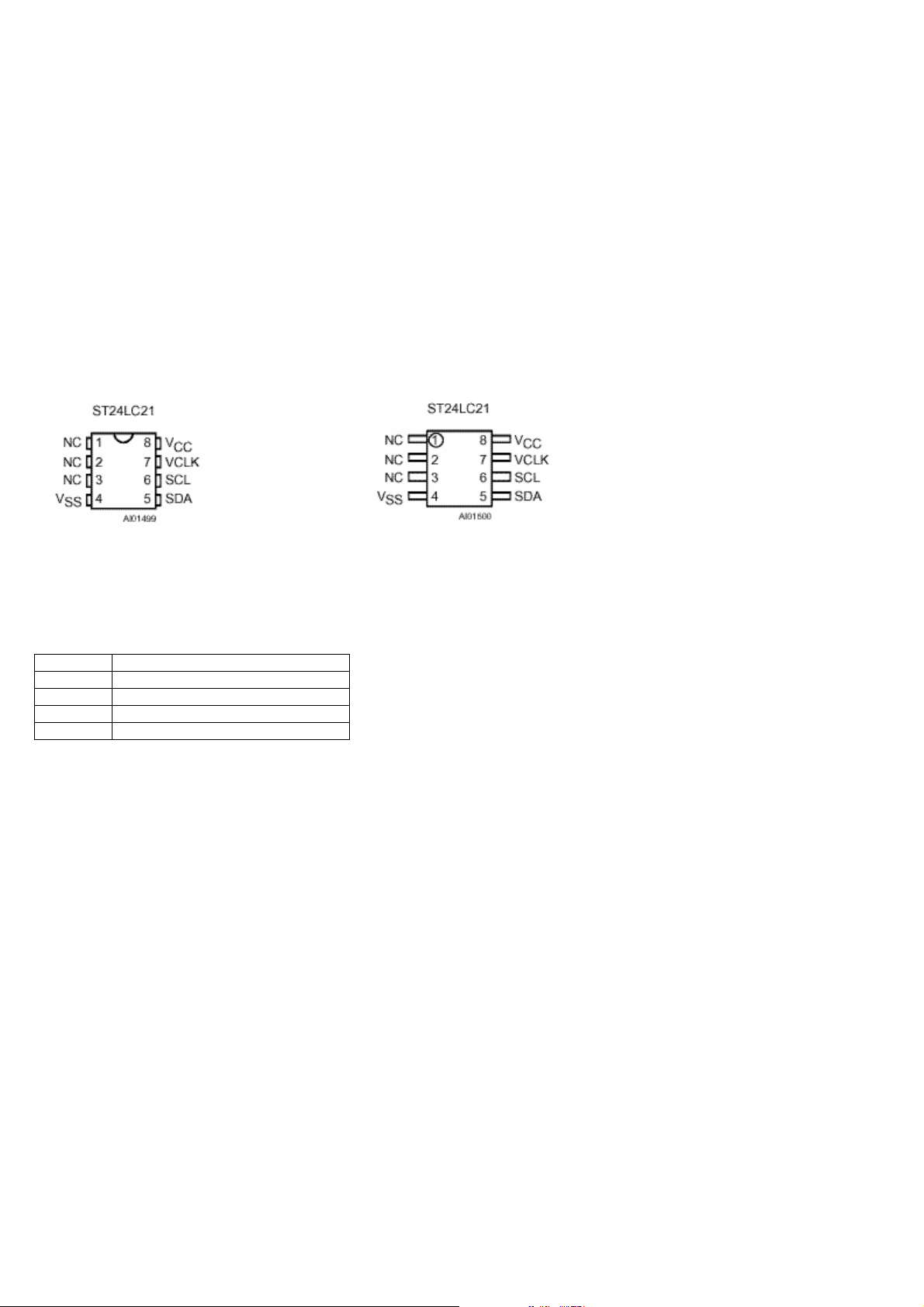
15.22. ST24LC21 28
15.22.1. Description 28
15.22.2. Features 29
15.22.3. Pin connections 29
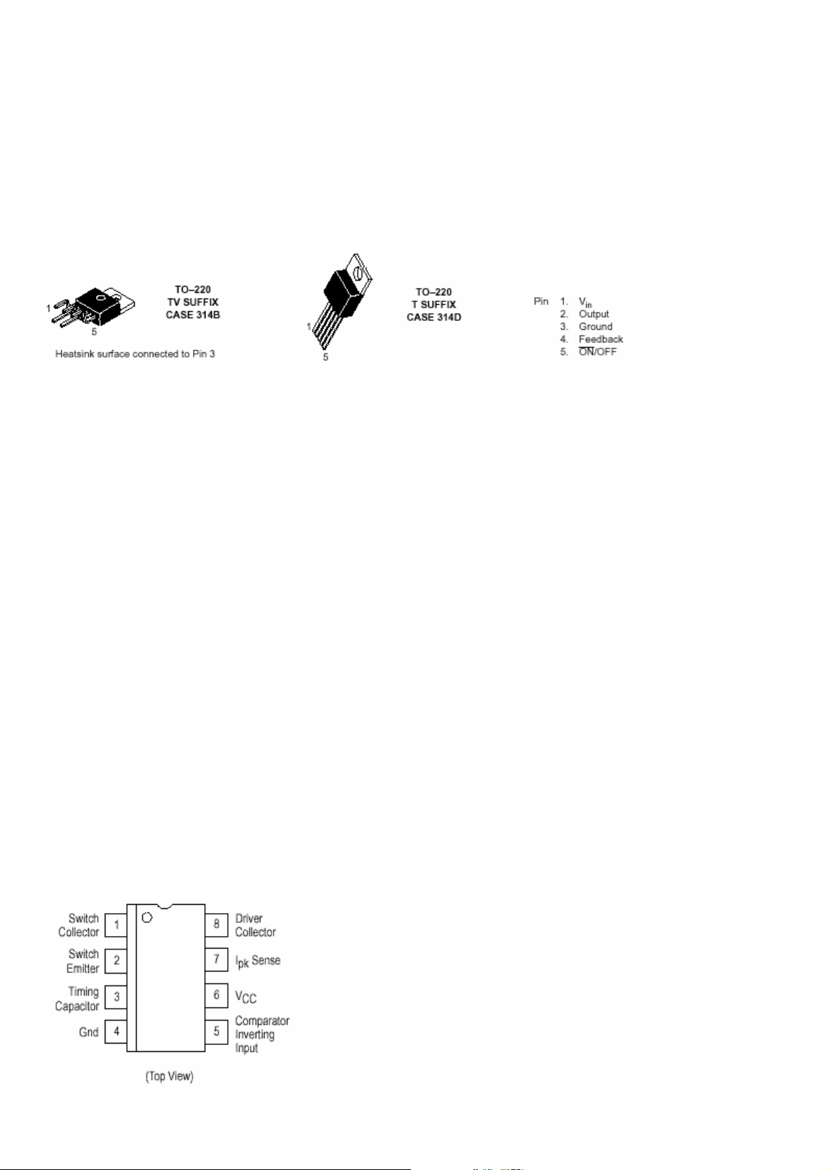
15.23. LM2576 29
15.23.1. General Description 29
15.23.2. Features 29
15.23.3. Pin description 30
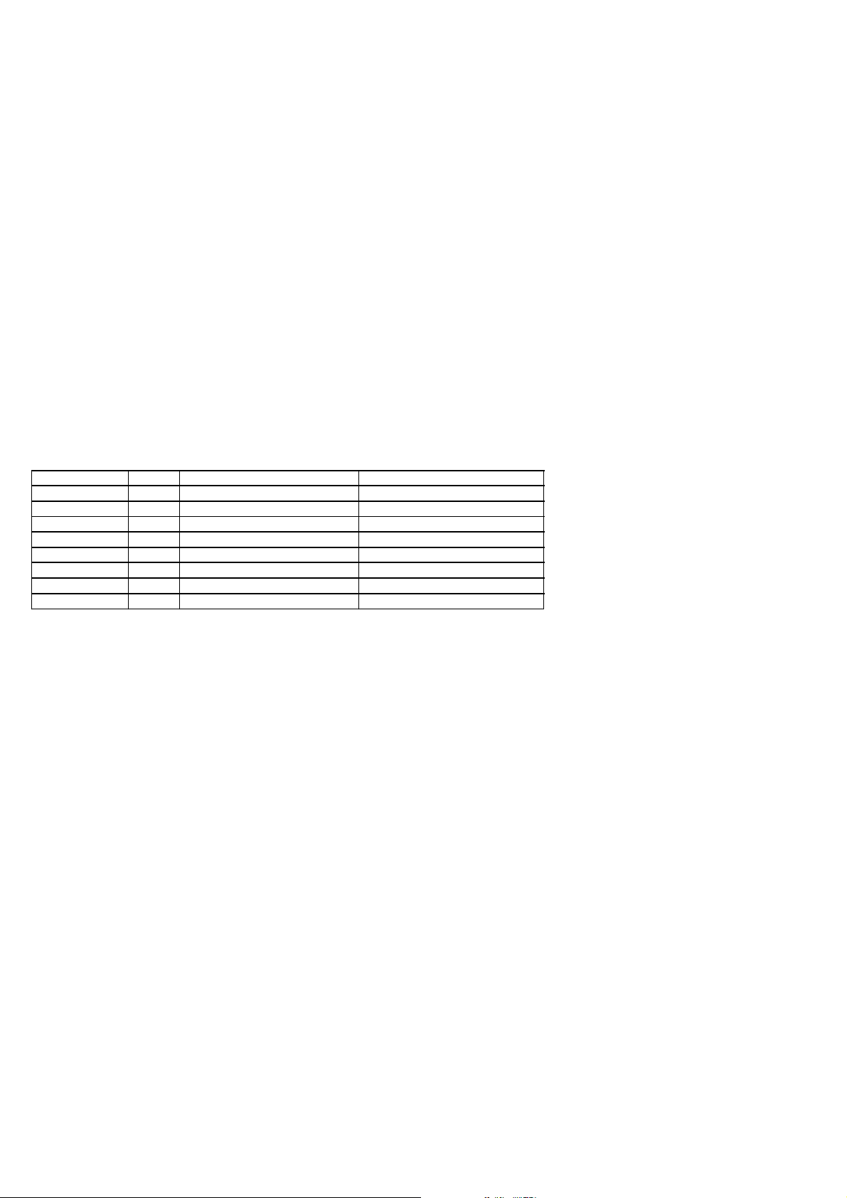
15.24. MC34063 30
15.24.1. Description 30
15.24.2. Features 30
15.24.3. Pin connections 30
15.25. TDA1308 31
15.25.1. General Description 31
15.25.2. Features 31
15.25.3. Pinning 31
TFT TV Service Manual
ii
Page 4

15.26. TDA9886 31
15.26.1. General Description 31
15.26.2. Features 31
15.26.3. Pinning 32
15.27. TPA3004D2 32
15.27.1. General Description 32
15.27.2. Features 32
15.27.3. Pinning 33
15.28. 34
15.29. µPA672T 34
15.29.1. General Description 34
15.29.2. Features 35
15.29.3. Pin Connection 35
15.30. VPC3230D 35
15.30.1. General Description 35
15.30.2. Pin Connections and Short Descriptions 35
15.31. MAD4868A 37
15.31.1. General Description 37
15.31.2. Features 37
15.31.3. Interfaces 37
15.31.4. Pinning 38
15.32. SVP-EX 59B 38
16. SERVICE MENU SETTINGS 38
16.1. Picture Adjust 39
16.2. SOUND1 39
16.3. SOUND 2 39
16.4. Options 39
17. CABLE CONNECTIONS 41
17.1. Cable Descriptions 42
18. APPENDIX A 43
18.1. ASSEMBLY DRAWING 43
19. APPENDIX B 44
19.1. BLOCK DIAGRAM 44
19.2. SCHEMATIC DIAGRAMS 45
19.2.1. Power Board 45
19.2.2. Main Board 1 (Tuner/IF/Audio) 46
19.2.3. Main Board 2 (In/Out) 47
19.2.4. Main Board 3 (VPC3230) 48
19.2.5. Main Board 4 (Video Decoder) 49
19.2.6. Main Board 5 (DDR RAM) 50
19.2.7. Main Board 6 (MCU Interface) 51
19.2.8. Main Board 7 (HDMI/DAC) 52
19.2.9. Main Board 8 (Power Supply) 53
19.2.10. Amplifier Board (D-Class Amplifier) 54
19.2.11. BAV Board (AV/HP/SV/LO) 55
19.3. CONNECTOR DIAGRAM 56
19.4. PCB LAYOUTS 57
19.4.1. Main Board 57
20. APPENDIX C 58
20.1. PARTLISTS 58
TFT TV Service Manual
iii
Page 5

1. PRECAUTION
2. SERVICE MENU ITEMS
2.1. SOUND 1
a) Menu Subwoofer => If ON, Subwoofer option is available in TV set, and the item is
visible in sound menu, else Subwoofer is not available. Default “ON”.
b) Subwoofer Level (dB) => This value is gain value of Subwoofer output in dB.
-30...12. Default “0” dB.
c) Subwoofer Corner Freq. (x10Hz) => Last low frequency value that is amplified. 5...40.
Default “22” x 10Hz = 220Hz.
d) Menu Equalizer => If ON, visible in sound menu, else invisible. Default “ON”.
e) Menu Headphone => If ON, visible in sound menu, else invisible. Default “ON”.
f) Menu Effect => If ON, visible in sound menu, else invisible. Default “ON”.
g) Menu Wide Sound => If ON, visible in sound menu, else invisible. Default “OFF”.
h) Menu Dynamic Bass => If ON, visible in sound menu, else invisible. Default “ON”.
i) Menu Virtual Dolby => If ON, visible in sound menu, else invisible. Default “ON”.
j) Carrier Mute => If ON, in the absence of an FM carrier the output is muted, else not.
Default “ON”.
k) Virtual Dolby Text => Active if VIRTUAL DOLBY is ON.According to the selection; seen
in sound menu as 3DS or VIRTUAL DOLBY. Default “3DS”.
2.2. SOUND 2
a) AVL => AVL is controlled from this menu by service user. ON/OFF. Default “ON”.
b) Menu AVL => If ON, AVL item is visible in sound menu, and AVL can be controlled from
sound menu by normal user, else AVL is invisible to normal user. ON/OFF. Default “ON”.
c) FM PRESCALE AVL ON => If AVL ON, set value in this item is used as prescale value
for the related standard. 0...127. Default “29”.
d) NICAM PRESCALE AVL ON => If AVL ON, set value in this item is used as prescale value
for the related standard. 0...127. Default “62”.
e) SCART PRESCALE AVL ON => If AVL ON, set value in this item is used as prescale value
for scart outputs. 0...127. Default “28”.
f) SCART VOLUME AVL ON => If AVL ON, set value in this item is used as volume value
for scart1 and scart2. 0...127. Default “116”.
TFT TV Service Manual
1
Page 6

g) FM PRESCALE AVL OFF => If AVL OFF, set value in this item is used as prescale value
for the related standard. 0...127. Default “15”.
h) NICAM PRESCALE AVL OFF => If AVL OFF, set value in this item is used as
prescale value for the related standard. 0...127. Default “35”.
i) SCART PRESCALE AVL OFF => If AVL OFF, set value in this item is used as
prescale value for scart outputs. 0...127. Default “14”.
j) SCART VOLOUME AVL OFF => If AVL OFF, set value in this item is used as volume
value for scart1 and scart2. 0...127. Default “122”.
2.3. Options
a) Burn-In Mode => If ON, full screen flashes in RED, GREEN, BLUE colors unless
“Menu” button on Remote Control or Keypad is pressed. This property is used to protect the T V
set from burning on the assembly lines in factory. This item becomes automatically OFF, when
First APS item is ON or Factory Reset is pressed. ON/OFF. Default OFF.
b) First APS => This bit is set “ON” in the factory. When the TV set is opened for
the first time it directs the user to make automatic search in both digital and analog modes.
c) APS Volume => After First APS function finishes, the volume of the TV is that value.
Default “10”.
d) AGC (dB) => Tuner AGC value. Default “15”.
e) Power-Up Mode =>Normal, Last State, Stand-by. Default “Last State”
f) PDP Working Hour =>Displays Panel Run time in decimal.
g) Factory Reset => OK to activate. When OK pressed on this item, factory defaults
loaded.
h) Enter Flash Mode =>OK to activate. When OK pressed on this item, flash mode is entered,
SW starts to wait for uploading the new SW.
2.4. Features
a) Blue Background => If ON, Blue Background is visible in Features Menu else not.
Default “ON”.
b) Menu Transparency => If ON, Menu Transparency is visible in Features Menu else not.
Default “ON”.
c) Menu Timeout => If ON, Menu Timeout is visible in Features Menu else not. Default
“ON”.
d) Backlight => If ON, Backlight is visible in Features Menu else not.Default “OFF”.
e) Single Tuner => If OFF, two tuners are available on the chassis. Fixed “ON”.
f) Dynamic WB => Default
TFT TV Service Manual
2
Page 7

2.5. Teletext
a) TOP TXT => ON/OFF
b) Fast TXT => ON/OFF
c) Teletext Language => Teletext Language may be controlled from this menu by service
user.
d) Txt Start RF
e) Txt Start Ext
f) Txt Start Mix
g) Menu Teletext Language => If ON, Teletext Language item is visible in Features Menu, and
Teletext Language can be controlled from Features Menu by normal user, else Teletext
Language is invisible to normal user.
2.6. Tuner Options
a) Switch Low Band
b) Switch Mid Band
c) Switch High Band
d) Boundry1 Low Byte
e) Boundry1 High Byte
f) Boundry2 Low Byte
g) Boundry2 High Byte
h) Control Byte
These values need to be filled in the factory acording to the tuner used on the chassis.
i) Store => OK to store; when the values are entered correctly OK needs to be pressed on this
item to store the values.
TFT TV Service Manual
3
Page 8

3. SOFTWARE UPDATE DESCRIPTION
3.1. ANALOG SOFTWARE UPDATE via SCART
STEP.1
Enter service menu by pressing the buttons “MENU”,”4”,”7”,”4”,”5” respectively.
STEP.2
Select “OPTIONS” from the service menu and “ENTER FLASH MODE”
STEP.3
Connect the Software Update Tool (17tr15-3) to parellel port of your PC.
STEP.4
Connect scart-end of the cable to Scart-1 (Ext-1).
STEP.5
Connect other-end of cable to “PL 2” socket on the Update Tool (17tr15-3)
STEP.6
Run IAPWriter.exe.
STEP.7
Click “load file” and load the required software.
TFT TV Service Manual
4
Page 9

3.2. ANALOG SOFTWARE UPDATE via I2C
STEP.1
Enter service menu by pressing the buttons “MENU”,”4”,”7”,”4”,”5” respectively.
STEP.2
Select “OPTIONS” from the service menu and “ENTER FLASH MODE”
STEP.3
Connect the Software Update Tool (17tr15-3) to parellel port of your PC.
STEP.4
Connect one-end of cable to “PL904” socket on the chassis socket MB15
STEP.5
Connect other-end of cable to “PL 2” socket on the Update Tool (17tr15-3)
STEP.6
Run IAPWriter.exe.
STEP.7
Click “load file” and load the required software.
TFT TV Service Manual
5
Page 10

3.3. EEPROM UPDATE via SCART
STEP.1.
Insert the EEROM tool(TR16) to SCART-1
STEP.2.
Enter service menu by pressing the buttons “MENU”,”4”,”7”,”4”,”5” respectively
STEP.3.
Press “YELLOW” colour button on the remote controller.
Then you will have two options
STEP.3.a
Press “RED” colour button to copy data of external EEPROM into internal one
STEP.3.b
Press “GREEN” colour button to copy data of internal EEPROM into external one
TFT TV Service Manual
6
Page 11

4. INTRODUCTION
26”W TFT TV is a progressive TV control system with built-in de-interlacer and scaler. It uses a 1366x768
( LG SLB2) panel with 16:9 aspect ratio.The TV is capable of operation in PAL, SECAM, NTSC (playback)
colour standards and multiple transmission standards as B/G, D/K, K’, I/I’, and L/L’ including German and
NICAM stereo. Sound system output is supplying 2x8W (10%THD) for stereo 8ȍ speakers. The chassis isinputs
equipped with many and outputs allowing it to be used as a center of a media system.
It supports following peripherals:
2 SCART sockets
1 AV input (CVBS + Stereo Audio)
1 SVHS input
1 Stereo Headphone input
1 Component input (YPbPr + Stereo Audio)
1 D-Sub 15 PC input
1 HDMI input
1 Stereo audio input for PC
1 Stereo audio output
5. TUNER
The tuners used in the design are combined VHF, UHF tuners suitable for CCIR systems B/G, K’, L, L’, I/I’, and
D/K. The tuning is available through the digitally controlled I
Tuners in use.
2
C bus (PLL). Below you will find info on one of the
General description of UV1316:
The UV1316 tuner belongs to the UV 1300 family of tuners, which are designed to meet a wide range of
applications. It is a combined VHF, UHF tuner suitable for CCIR systems B/G, H, L, L’, I and I’. The low IF output
impedance has been designed for direct drive of a wide variety of SAW filters with sufficient suppression of triple
transient.
Features of UV1316:
1. Member of the UV1300 family small sized UHF/VHF tuners
2. Systems CCIR: B/G, H, L, L’, I and I’; OIRT: D/K
3. Digitally controlled (PLL) tuning via I
2
C-bus
4. Off-air channels, S-cable channels and Hyperband
5. World standardised mechanical dimensions and world standard pinning
6. Compact size
7. Complies to “CENELEC EN55020” and “EN55013”
Pinning:
1. Gain control voltage (AGC) : 4.0V, Max: 4.5V
2. Tuning voltage
3. I²C-bus address select : Max: 5.5V
4. I²C-bus serial clock : Min:-0.3V, Max: 5.5V
5. I²C-bus serial data : Min:-0.3V, Max: 5.5V
6. Not connected
7. PLL supply voltage : 5.0V, Min: 4.75V, Max: 5.5V
8. ADC input
9. Tuner supply voltage : 33V, Min: 30V, Max: 35V
10. Symmetrical IF output 1
11. Symmetrical IF output 2
6. IF PART (TDA9886)
The TDA9886 is an alignment-free multistandard (PAL, SECAM and NTSC) vision and sound IF signal PLL. The
following figure shows the simplified block diagram of the integrated circuit.
The integrated circuit comprises the following functional blocks:
VIF amplifier, Tuner and VIF-AGC, VIF -AGC detector, Frequency Phase-Locked Loop (FPLL) detector, VCO and
divider, Digital acquisition help and AFC, Video demodulator and amplifier, Sound carrier trap, SIF amplifier, SIF-AGC
TFT TV Service Manual
7
Page 12
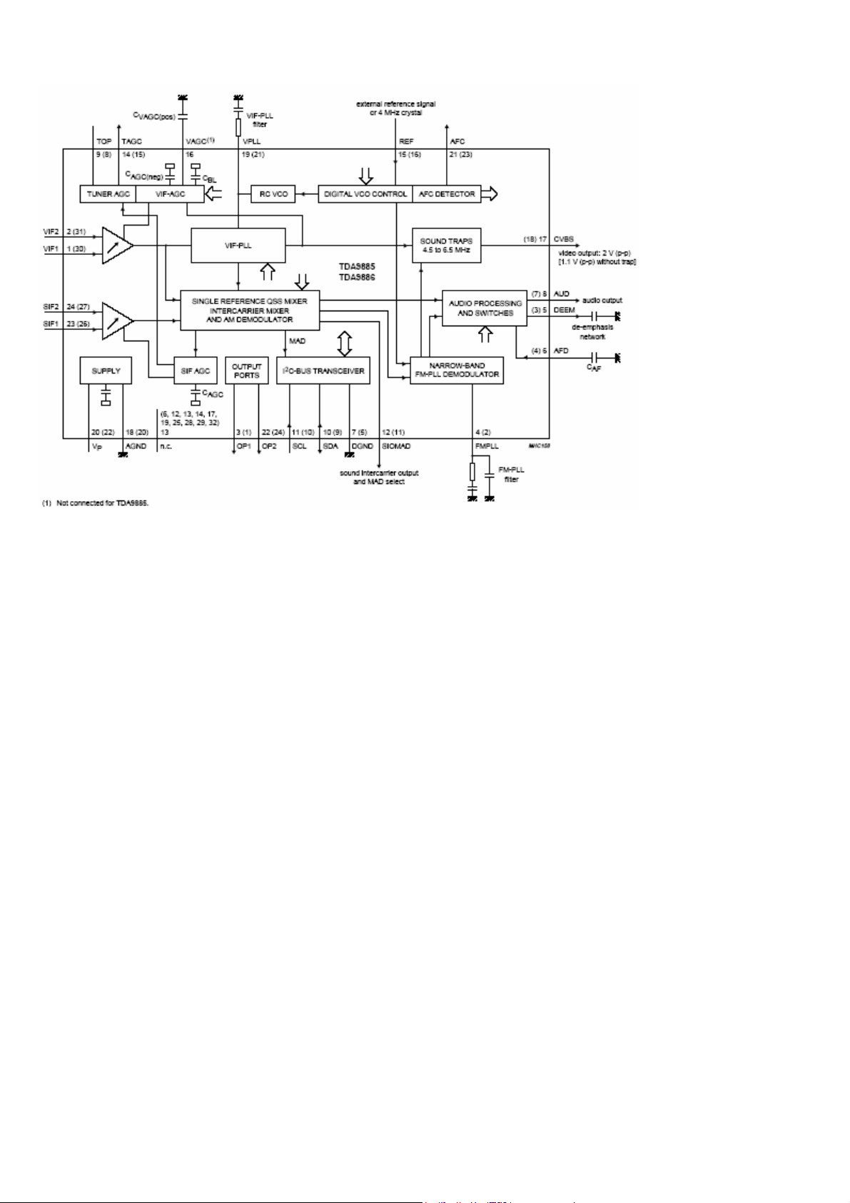
detector, Single reference QSS mixer, AM demodulator, FM demodulator and acquisition help, Audio amplifier and
mute time constant,
I²C-bus transceivers and MAD (module address), Internal voltage stabilizer.
7. MULTI STANDARD SOUND PROCESSOR
The MSP34x0G family of single-chip Multistandard Sound Processors covers the sound processing of all analogue TVStandards worldwide, as well as the NICAM digital sound standards. The full TV sound processing, starting with analogue
sound IF signal-in, down to processed analogue AF-out, is performed on a single chip.
These TV sound processing ICs include versions for processing the multichannel television sound (MTS) signal
conforming to the standard recommended by the Broadcast Television Systems Committee (BTSC). The DBX
noise reduction, or alternatively, Micronas Noise Reduction (MNR) is performed alignment free. Other processed
standards are the Japanese FM-FM multiplex standard (EIA-J) and the FM Stereo Radio standard.
Current ICs have to perform adjustment procedures in order to achieve good stereo separation for BT SC and EIA-J. The
MSP 34x1G has optimum stereo performance without any adjustments.
8. VIDEO SWITCH TEA6415
In case of three or more external sources are used, the video switch IC T EA6415 is used. The main function of this device is
to switch 8 video-input sources on the 6 outputs.
Each output can be switched on only one of each input. On each input an alignment of the lowest level of the
signal is made (bottom of sync. top for CVBS or black level for RGB signals).
Each nominal gain bet ween any input and output is 6.5dB.For D2MAC or Chroma signal the alignment is switched off by
forcing, with an external resistor bridge, 5VDC on the input. E ach input can be used as a normal input or as a MAC or
Chroma input (with external Resistor Bridge). All the switching possibilities are changed through the BUS. Driving 75ohm
load needs an exter nal resistor. It is possible to have the same input connected to several outputs.
9. AUDIO AMPLIFIER STAGE WITH TPA3004D2
The TPA3004D2 is a 12-W (per channel) efficient, Class-D audio amplifier for driving bridged-tied stereo speakers. The
TPA3004D2 can drive stereo speakers as low as 4 7KHKLJKHIILFLHQF\RIWKH73$'HOLPLQDWHVWKHQHHGIRU
external heatsinks when playing music.
Stereo speaker volume is controlled with a dc voltage applied to the volume control terminal offering a range of gain from –
40 dB to 36 dB. Line outputs, for driving external headphone amplifier inputs, are also dc voltage controlled with a range
ofgainfrom–56dBto20dB.
An integrated 5-V regulated supply is provided for powering an external headphone amplifier.
TFT TV Service Manual
8
Page 13

10. POWER SUPPLY (SMPS)
The DC voltages required at various parts of the chassis are provided by an SMPS transformer controlled by the IC
MC44608, which is designed for driving, controlling and protecting switching transistor of SMPS. The transformer
generates 145V for FBT input, +/-14V for audio amplifier, 5V and 3.3V stand by voltage and 8V, 12V and 5V supplies for
other d ifferent parts of the chassis.
An optocoupler is used to control the regulation of line voltage and stand-by power consumption. There is a regulation
circuit i n secondary side. This circuit produces a control voltage according to the changes in 145V DC voltage, via an
optocoupler (TCET1102G) to pin3 of the IC.
During the switch on period of the transistor, energy is stored in the transformer. During the switch off period
energy is fed to the load via secondary winding. By varying switch-on time of the power transistor, it controls
each portion of energy transferred to the second side such that the output voltage remains nearly independent
of load variations.
11. MICROCONTROLLER
The Micronas SDA 55xx TV microcontroller is dedicated to 8 bit applications for TV control and provides dedicated
graphic features designed for modern low class to mid range TV sets. The SDA 55xx provides also an integrated
general purposefully 8051-compatible microcontroller with specific hardware features especially suitable in TV sets.
The microcontroller core has been enhanced to provide powerful features such as memory banking, data pointers and
additional interrupts, etc. The internal XRAM consists of up to 16 kBytes. The microcontroller provides an internal
ROM of up to 128 kBytes. ROMless versions can access up to 1 MByte of external RAM and ROM. The 8-bit
microcontroller runs at 33.33 MHz internal clock. SDA 55xx is realized in 0.25 micron technology with 2.5 V supply
voltage for the core and 3.3 V for the I/O port pins to make them TTL compatible. Based on the SDA 55xx
microcontroller the MINTS software package was developed and provides dedicated device drivers for many Micronas
video & audio products and includes a full blown TV control SW for the PEPER application chassis. The SDA 55xx is
also supported with powerful design tools like emulators from Hitex, Kleinhenz, iSystems, the Keil C51 Compiler and
TEDIpro OSD development SW by Tara Systems.
12. SERIAL ACCESS CMOS 4Kx8(32KBit)EEPROM 24C32A
The Microchip Technology Inc. 24AA32A/24LC32A(24XX32A*) is a 32 Kbit Electrically Erasable PROM. The device is
organized as four blocks of 8K x 8-bitmemory with a 2-wire serial interface. Low-voltage design permits operation
down to 1.8V, with standby and active currents of only 1μA and 1mA, respectively. It has been developed for
advanced, low-power applications such as personal communications or data acquisition. The 24XX32A also has a
page write capability for up to 32 bytes of data. Functional address lines allow up to eight devices on the same bus, for
up to 256Kbits address space.
13. CLASS AB STEREO HEADPHONE DRIVER TDA1308
The TDA1308 is an integrated class AB stereo headphone driver contained in a DIP8 plastic package. The
deviceisfabricatedina1mmCMOSprocessandhasbeenprimarilydevelopedforportabledigitalaudio
applications.
14. SAW FILTERS
K9656M:
Standard:
•B/G
• D/K
•I
• L/L’
Features
• TV IF audio filter with two channels
• Channel 1 (L’) with one pass band for sound carriers at 40.40 MHz (L’) and 39.75 MHz (L’- NICAM)
• Channel 2 (B/G, D/K, L, I) with one pass band for sound carriers between 32.35 MHz and 33.40 MHz
Terminals
• Tinned CuFe alloy
Pin configuration
1Input
2 Switching input
3 Chip carrier - ground
4Output
5Output
TFT TV Service Manual
9
Page 14

K3958M:
Standard:
•B/G
• D/K
•I
• L/L’
Features
• TV IF video filter with Nyquist slopes at 33.90 MHz and 38.90 MHz
• Constant group delay
Terminals
Tinned CuFe alloy
Pin configuration
1Input
2 Input - ground
3 Chip carrier - ground
4 Output
5 Output
15. IC DESCRIPTIONS
TEA6415C
24LC02
24C32
74LVC14A
TEA6420D
CS4334
GAL16LV8
K6R4008V1
KA278R33
LM1117
LM317T
LM809
MSP3411G
M29W040B
MC33202
PCF8574
TSOP1836
PI5V330
SDA5550
SII9993
SN74CB3Q3305
ST24LC21
LM2576
MC34063
TDA1308
TDA9886T
TPA3004D2
μPA672T
VPC3230D
MAD4868A
SVP EX-59B
15.1. TEA6415C
15.1.1. General Description
The main function of the IC is to switch 8 video input sources on 6 outputs. Each output can be switched on only
one of each input. On each input an alignment of the lowest level of the signal is made (bottom of synch. top for
CVBS or black level for RGB signals). Each nominal gain between any input and output is 6.5dB. For D2MAC or
Chroma signal the alignment is switched off by forcing, with an external resistor bridge, 5 V
DC on the input. Each
input can be used as a normal input or as a MAC or Chroma input (with external resistor bridge). All the
switching possibilities are changed through the BUS. Driving 75ORDGQHHGVDQH[WHUQDOWUDQVLVWRU,WLVSRVVLEOH
TFT TV Service Manual
10
Page 15

to have the same input connected to several outputs. The starting configuration upon power on (power supply: 0
to 10V) is undetermined. In this case, 6 words of 16 bits are necessary to determine one configuration. In other
case, 1 word of 16 bits is necessary to determine one configuration.
15.1.2.
• 20MHz Bandwidth
• Cascadable with another TEA6415C (Internal address can be changed by pin 7 voltage)
• 8 Inputs (CVBS, RGB, MAC, CHROMA,...)
• 6 Outputs
• Possibility of MAC or chroma signal for each input by switching-off the clamp with an external resistor bridge
• Bus controlled
• 6.5dB gain between any input and output
• 55dB crosstalk at 5mHz
• Fully ESD protected
15.1.3.
1. Input : Max : 2Vpp, Input Current: 1mA, Max : 3mA
2. Data : Low level : -0.3V Max: 1.5V,
3. Input : Max : 2Vpp, Input Current: 1mA, Max : 3mA
4. Clock : Low level : -0.3V Max: 1.5V,
5. Input : Max : 2Vpp, Input Current: 1mA, Max : 3mA
6. Input : Max : 2Vpp, Input Current: 1mA, Max : 3mA
7. Prog
8. Input : Max : 2Vpp, Input Current: 1mA, Max: 3mA
9. Vcc : 12V
10. Input : Max : 2Vpp, Input Current: 1mA, Max : 3mA
11. Input : Max : 2Vpp, Input Current: 1mA, Max : 3mA
12. Ground
13. Output : 5.5Vpp, Min : 4.5Vpp
14. Output : 5.5Vpp, Min : 4.5Vpp
15. Output : 5.5Vpp, Min : 4.5Vpp
16. Output : 5.5Vpp, Min : 4.5Vpp
17. Output : 5.5Vpp, Min : 4.5Vpp
18. Output : 5.5Vpp, Min : 4.5Vpp
19. Ground
20. Input : Max : 2Vpp, Input Current : 1mA, Max : 3mA
Features
Pinning
High level : 3.0V Max : Vcc+0.5V
High level : 3.0V Max : Vcc+0.5V
TFT TV Service Manual
11
Page 16
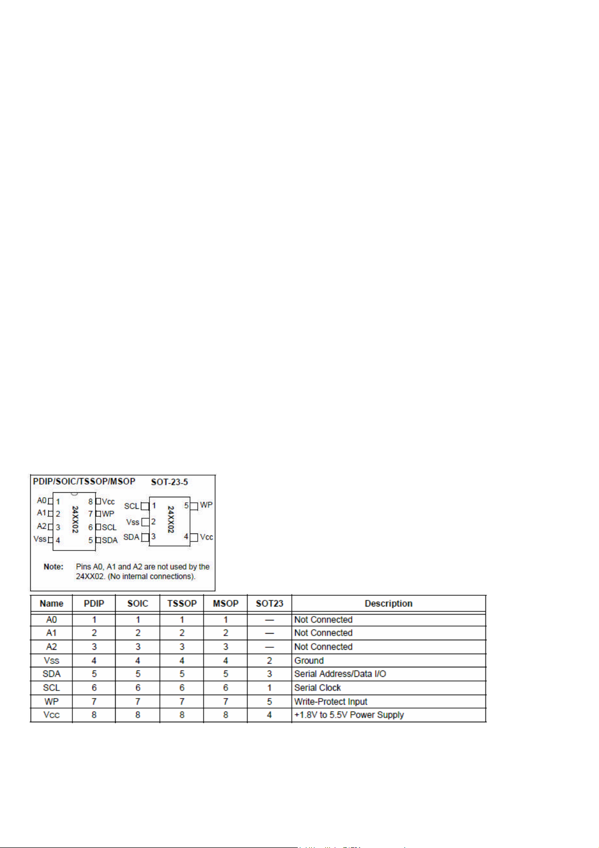
15.2. 24LC02
15.2.1. Description
The Microchip Technology Inc. 24AA02/24LC02B (24XX02*) is a 2 Kbit Electrically Erasable PROM. The device
is organized as one block of 256 x 8-bit memory with a 2-wire serial interface. Low -voltage design permits
operation down to 1.8V, with standby and active currents of only 1μA and 1mA, respectively. The 24XX02 also
has a page write capability for up to 8 bytes of data.
15.2.2.
• Single supply with operation down to 1.8V
• Low-power CMOS technology
-1mA active current typical
-1μA standby current typical (I-temp)
• Organized as 1 block of 256 bytes (1 x 256 x 8)
• 2-wire serial interface bus, I
• Schmitt Trigger inputs for noise suppression
• Output slope control to eliminate ground bounce
• 100 kHz (24AA02) and 400 kHz (24LC02B) compatibility
• Self-timed write cycle (including auto-erase)
• Page write buffer for up to 8 bytes
• 2ms typical write cycle time for page write
• Hardware write-protect for entire memory
• Can be operated as a serial ROM
• Factory programming (QTP) available
• ESD protection > 4,000V
• 1,000,000 erase/write cycles
• Data retention > 200 years
• 8-lead PDIP, SOIC, TSSOP and MSOP packages
• 5-lead SOT-23 package
• Pb-free finish available
• Available for extended temperature ranges:
-Industrial (I): -40°C to +85°C
-Automotive (E): -40°C to +125°C
Features
2
C compatible
15.2.3.
Pinning
TFT TV Service Manual
12
Page 17
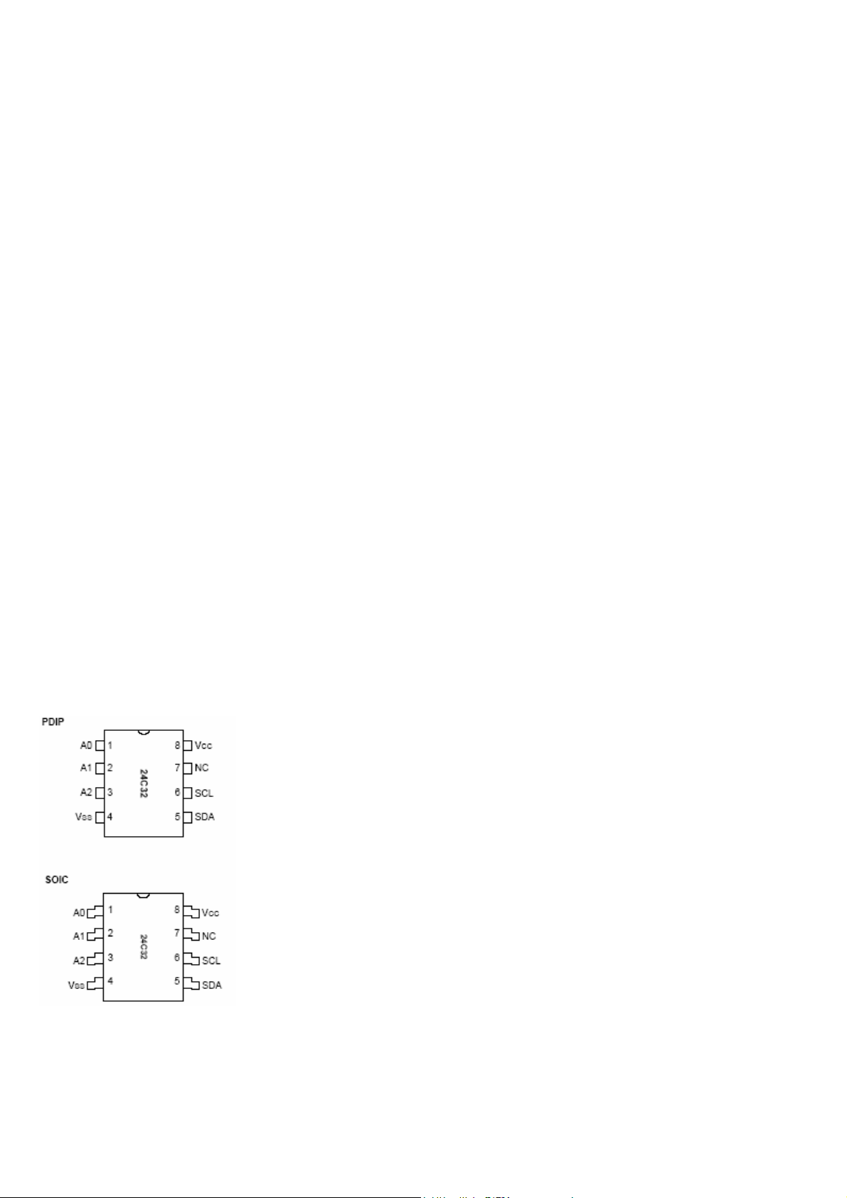
15.3. 24C32
15.3.1. General Description
The Microchip Technology Inc. 24C32 is a 4K x 8 (32K bit) Serial Electrically Erasable PROM. This device has
been developed for advanced, low power applications such as personal communications or data acquisition.
The 24C32 features an input cache for fast write loads with a capacity of eight 8-byte pages, or 64 bytes. It also
features a fixed 4K-bit block of ultra-high endurance memory for data that changes frequently. The 24C32 is
capable of both random and sequential reads up to the 32K boundary. Functional address lines allow up to 8 24C32 devices on the same bus, for up to 256K bits address space. Advanced CMOS technology makes this
device ideal for low-power non-volatile code and data applications.
15.3.2.
• Voltage operating range: 4.5V to 5.5V
- Peak write current 3 mA at 5.5V
- Maximum read current 150μA at 5.5V
- Standby current 1μA typical
• Industry standard two-wire bus protocol, I
-Including 100 kHz and 400 kHz modes
• Self-timed write cycle (including auto-erase)
• Power on/off data protection circuitry
• Endurance:
- 10,000,000 Erase/Write cycles guaranteed for High Endurance Block
- 10,000,000 E/W cycles guaranteed for Standard Endurance Block
• 8 byte page, or byte modes available
• 1 page x 8 line input cache (64 bytes) for fast write
loads
• Schmitt trigger, filtered inputs for noise suppression
• Output slope control to eliminate ground bounce
• 2 ms typical write cycle time, byte or page
• Up to 8 chips may be connected to the same bus for up to 256K bits total memory
• Electrostatic discharge protection > 4000V
• Data retention > 200 years
• Temperature ranges:
-Commercial (C): 0°C to +70°C
-Industrial (I): -40°C to +85°C
15.3.3.
Features
Pinning
2
C compatible
TFT TV Service Manual
13
Page 18

15.3.4.
PIN DESCRIPTIONS
A0, A1, A2 Chip Address Inputs
The A0...A2 inputs are used by the 24C32 for multiple device operation and conform to the two-wire bus standard. The levels applied to these pins define the address block occupied by the device in the address map. A
particular device is selected by transmitting the corresponding bits (A2, A1, and A0) in the control byte.
SDA Serial Address/Data Input/Outpu
This is a bidirectional pin used to transfer addresses and data into and data out of the device. It is an open drain
terminal; therefore the SDA bus requires a pull-up resistor to VCC (typical 10KQ for 100 kHz, 1KQ for 400 kHz).
For normal data transfer SDA is allowed to change only during SCL low. Changes during SCL high are reserved
for indicating the START and STOP conditions.
SCL Serial Clock
This input is used to synchronize the data transfer from and to the device.
PIN Function Table
t
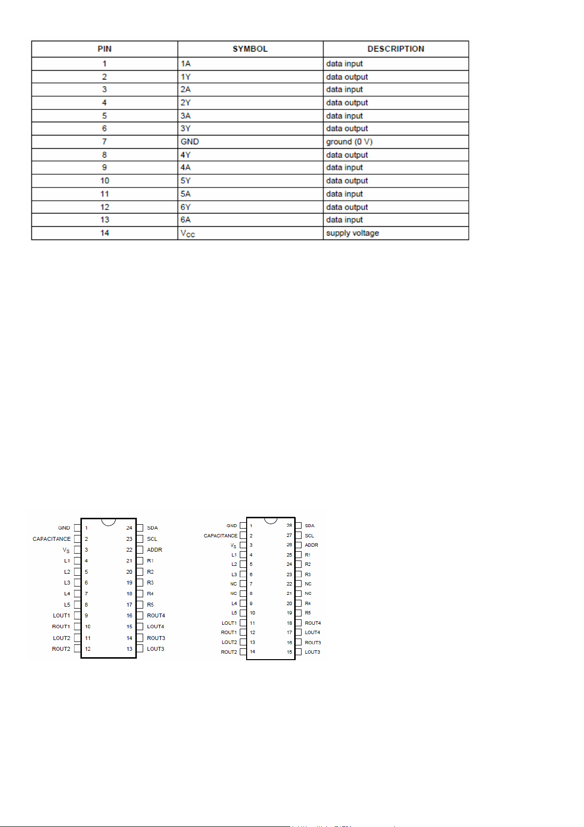
15.4. 74LVC14A
15.4.1. Description
The 74LVC14A is a high-performance, low-power, low-voltage, Si-gate CMOS device, superior to most advanced
CMOS compatible TTL families. Inputs can be driven from either 3.3 or 5V devices. This feature allows the use of
these devices as translators in a mixed 3.3 and 5V environment. The 74LVC14A provides six inverting buffers with
Schmitt-trigger action. It is capable of transforming slowly changing input signals into sharply defined, jitter-free output
signals.
15.4.2. Features
• Wide supply voltage range from 1.2 to 3.6 V
• CMOS low power consumption
• Direct interface with TTL levels
• Inputs accept voltages up to 5.5 V
• Complies with JEDEC standard no.8-1A
• ESD protection:
HBM EIA/JESD22-A114-A exceeds 2000V
MM EIA/JESD22-A115-A exceeds 200V.
• Specified from -40 to +85C and -40 to +125C.
15.4.3. Pinning
TFT TV Service Manual
14
Page 19
15.5. TEA6420
15.5.1. Features
• 5 Stereo Inputs
• 4 Stereo Outputs
• Gain Control 0/2/4/6dB/Mute for each Output
• Cascadable (2 different addresses)
• Serial Bus Controlled
•VerylowNoise
• Very low Distortion
15.5.2.
The TEA6420 switches 5 stereo audio inputs on4stereo outputs. All the switching possibilities are changed
through the I
15.5.3.
Description
2
C bus.
Pin Connections
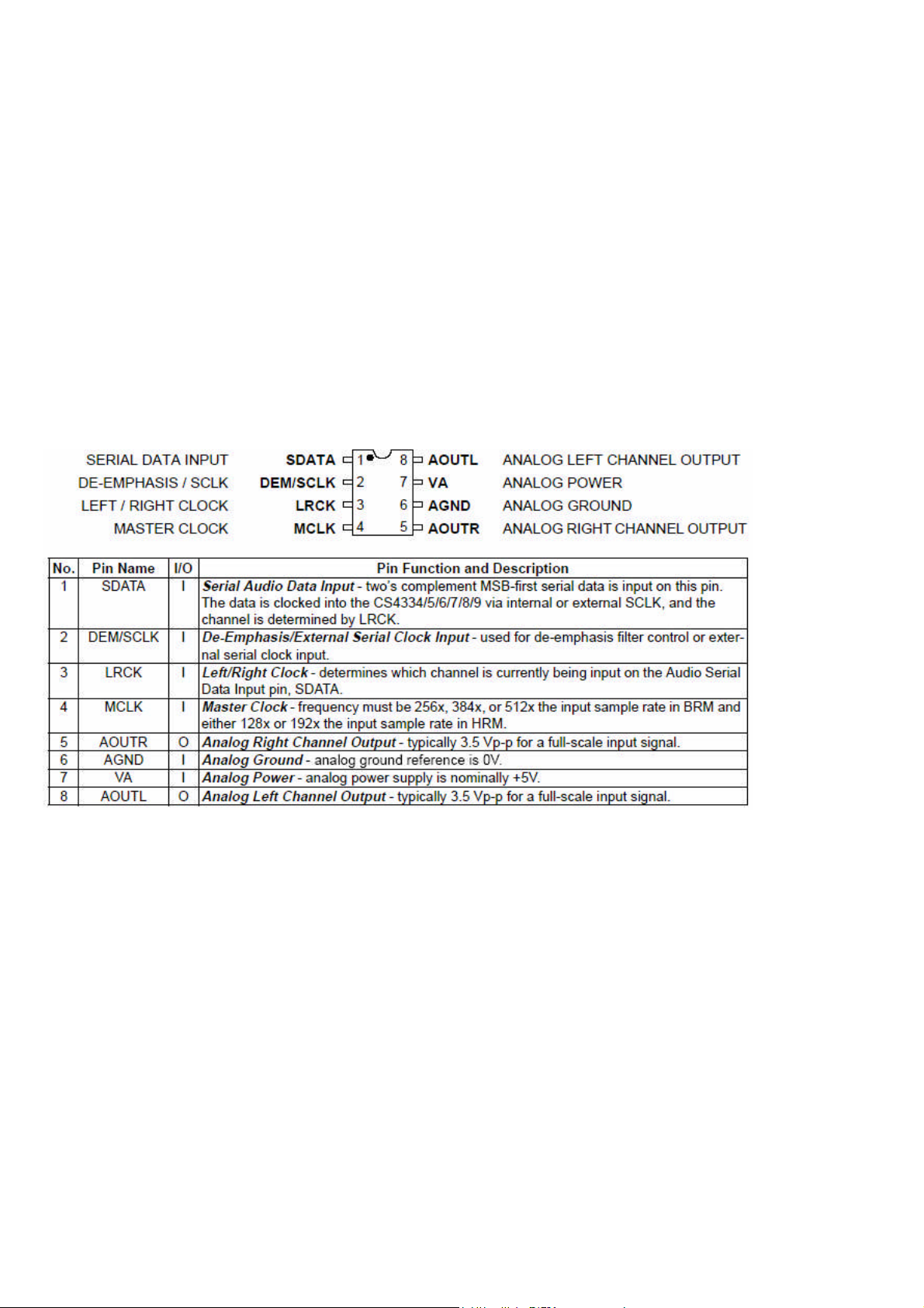
15.6. CS4334
15.6.1. Features
• Complete Stereo DAC System: Interpolation, D/A, Output Analog Filtering
• 24-Bit Conversion
TFT TV Service Manual
15
Page 20
•
96 dB Dynamic Range
• -88 dB THD+N
• Low Clock Jitter Sensitivity
• Single +5V Power Supply
• Filtered Line Level Outputs
• On-Chip Digital De-emphasis
• Popgaurd® Technology
• Functionally Compatible with CS4330/31/33
15.6.2. General Description
The CS4334 family members are complete, stereo digital-to-analog output systems including interpolation, 1 bitD/A conversion and output analog filtering in an 8-pinpackage. The CS4334/5/6/7/8/9 support all major audio
data interface formats, and the individual devices differ only in the supported interface format. The CS4334
family is based on delta-sigma modulation, where the modulator output controls the reference voltage input to
an ultra-linear analog low-pass filter. This architecture allows for infinite adjustment of sample rate between 2
kHz and 100 kHz simply by changing the master clock frequency. The CS4334 family contains on-chip digital
de-emphasis, operates from a single +5V power supply, and requires minimal support circuitry. These features
are ideal for set-top boxes, DVD players, SVCD players, and A/V receivers.
15.6.3.
Pin Descriptions
15.7. GAL16LV8
15.7.1. Description
The GAL16LV8D, at 3.5 ns maximum propagation delay time, provides the highest speed performance available
in the PLD market. The GAL16LV8C can interface with both 3.3V and 5Vsignal levels. The GAL16LV8 is
manufactured using Lattice Semiconductor's advanced 3.3V E
Electrically Erasable (E
2
) floating gate technology. High speed erase times (<100ms) allow the devices to be
2
CMOS process, which combines CMOS with
reprogrammed quickly and efficiently.
The 3.3V GAL16LV8 uses the same industry standard 16V8 architecture as its 5V counterpart and supports all
architectural features such as combinatorial or registered macrocell operations.
Unique test circuitry and reprogrammable cells allow complete AC, DC, and functional testing during
manufacture. As a result, Lattice Semiconductor delivers 100% field programmability and functionality of all
GAL products. In addition, 100 erase/write cycles and data retention in excess of 20 years are specified.
15.7.2.
Features
• HIGH PERFORMANCE E2CMOS® TECHNOLOGY
- 3.5 ns Maximum Propagation Delay
- Fmax = 250 MHz
TFT TV Service Manual
16
Page 21
- 2.5 ns Maximum from Clock Input to Data Output
- UltraMOS® Advanced CMOS Technology
• 3.3V LOW VOLTAGE 16V8 ARCHITECTURE
- JEDEC-Compatible 3.3V Interface Standard
- 5V Compatible Inputs
- I/O Interfaces with Standard 5V TTL Devices (GAL16LV8C)
• ACTIVE PULL-UPS ON ALL PINS (GAL16LV8D Only)
•E2CELLTECHNOLOGY
- Reconfigurable Logic
- Reprogrammable Cells
- 100% Tested/100% Yields
- High Speed Electrical Erasure (<100ms)
- 20 Year Data Retention
• EIGHT OUTPUT LOGIC MACROCELLS
- Maximum Flexibility for Complex Logic Designs
- Programmable Output Polarity
• PRELOAD AND POWER-ON RESET OF ALL REGISTERS
- 100% Functional Testability
• APPLICATIONS INCLUDE:
- Glue Logic for 3.3V Systems
- DMA Control
- State Machine Control
- High Speed Graphics Processing
- Standard Logic Speed Upgrade
• ELECTRONIC SIGNATURE FOR IDENTIFICATION
• LEAD-FREE PACKAGE OPTIONS
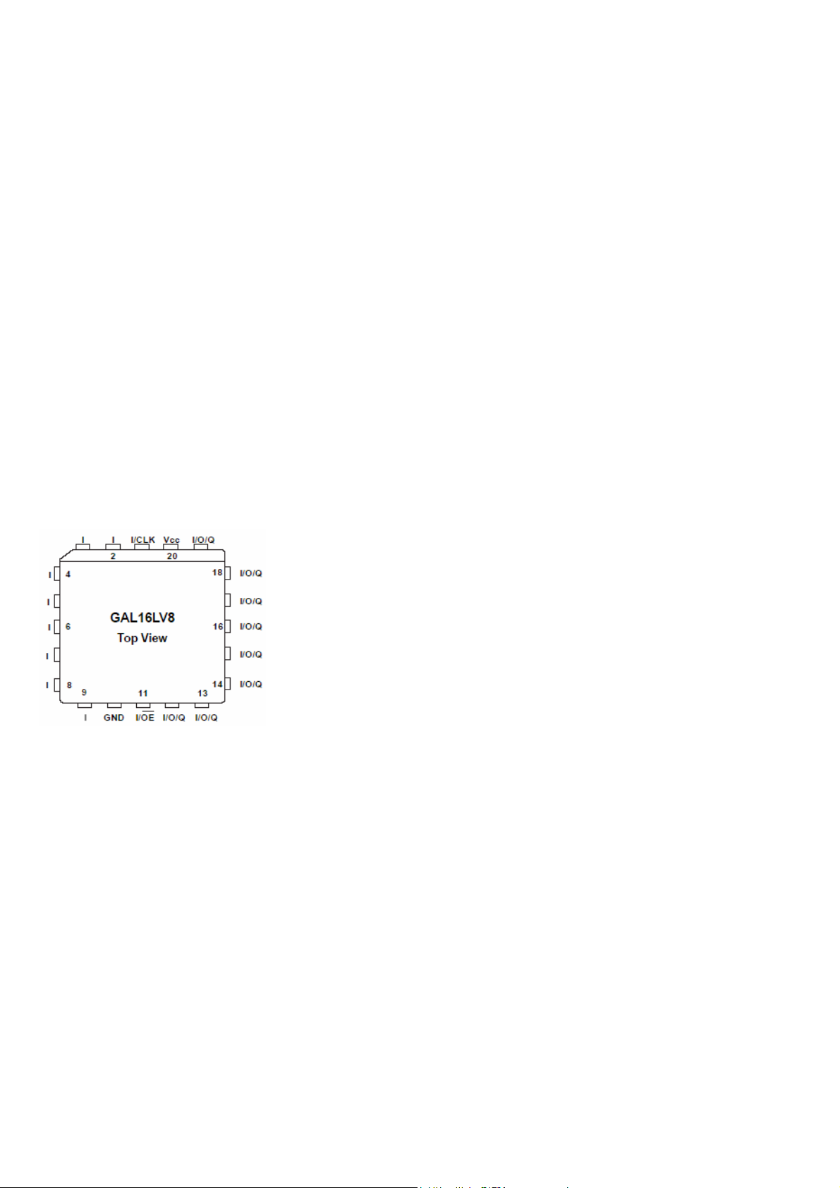
15.7.3.
Pin connections
15.8. K6R4008V1D
15.8.1. Description
The K6R4008V1D is a 4,194,304-bit high-speed Static Random Access Memory organized as 524,288 words by
8 bits. TheK6R4008V1D uses 8 common input and output lines and has an output enable pin which operates
faster than address access time at read cycle. The device is fabricated using SAMSUNG's advanced CMOS
process and designed for high-speed circuit technology. It is particularly well suited for use in high-density high-
speed system applications. The K6R4008V1D is packaged in a 400 mil 36-pin plastic SOJ and 44-pin plastic
TSOP type II.
15.8.2.
• Fast Access Time 8, 10ns(Max.)
• Low Power Dissipation
- Standby (TTL) : 20mA(Max.)
- Operating K6R4008V1D-08 : 80mA(Max.)
TFT TV Service Manual
Features
(CMOS) : 5mA(Max.)
17
Page 22
K6R4008V1D-10 : 65mA(Max.)
• Single 3.3 ±0.3V Power Supply
• TTL Compatible Inputs and Outputs
• Fully Static Operation
- No Clock or Refresh required
• Three State Outputs
• Center Power/Ground Pin Configuration
• Standard Pin Configuration
K6R4008V1D-J : 36-SOJ-400
K6R4008V1D-K : 36-SOJ-400(Lead-Free)
K6R4008V1D-T : 44-TSOP2-400BF
K6R4008V1D-U : 44-TSOP2-400BF(Lead-Free)
• Operating in Commercial and Industrial Temperature range.
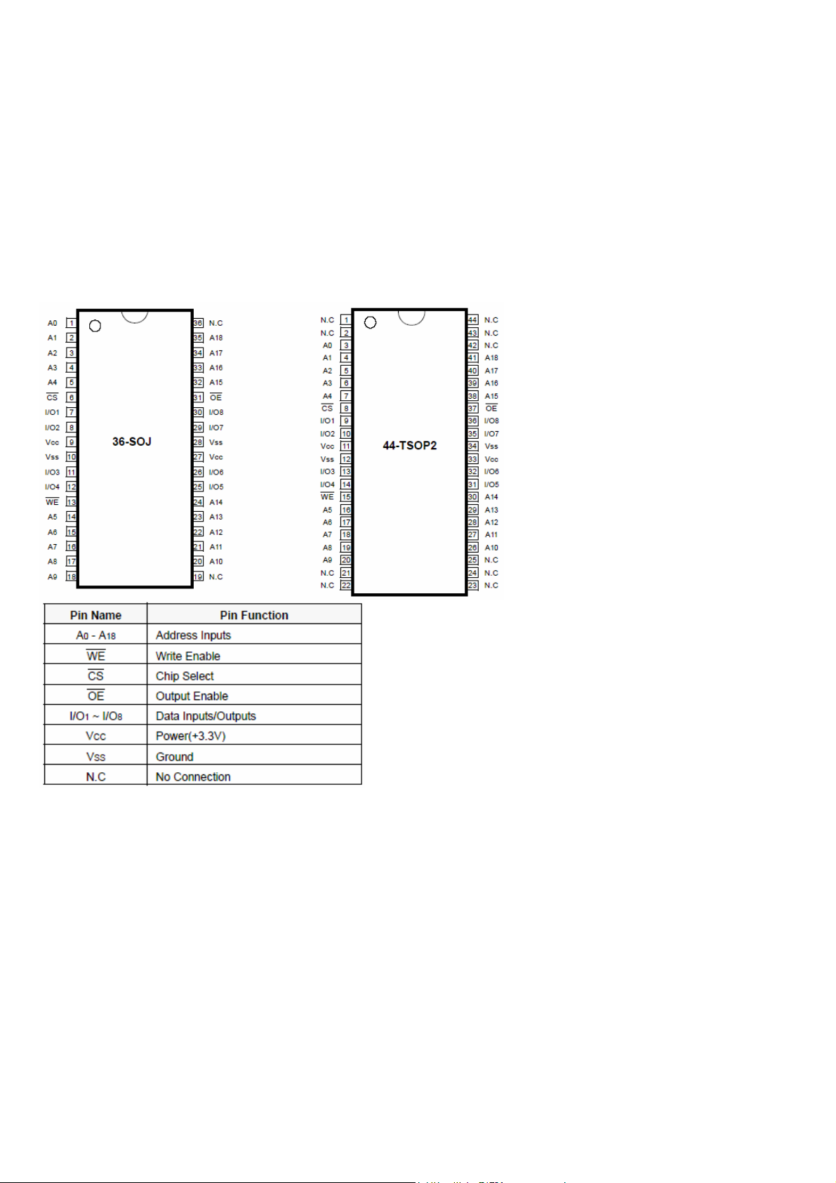
15.8.3.
Pin Description
15.9. KA278R33
15.9.1. Features
• 2A / 3.3V Output low dropout voltage regulator
• TO220 Full-Mold package (4PIN)
• Overcurrent protection, Thermal shutdown
• Overvoltage protection, Short-Circuit protection
• With output disable function
15.9.2.
The KA278R33 is a low-dropout voltage regulator suitable for various electronic equipments. It provides
constant voltage power source with TO-220 4 lead full mold package. Dropout voltage of KA278R33 is below
TFT TV Service Manual
Description
18
Page 23
0.5V in full rated current (2A). This regulator has various function such as peak current protection, thermal shut
down, overvoltage protection and output disable function.
15.10. LM1117
15.10.1. General Description
The LM1117 is a series of low dropout voltage regulators with a dropout o f 1.2V at 800mA of load current. It has the same
pin-out as Natio nal Semiconductor’s industry standard LM317. The LM1117 is available in an adjustable version, which
can set the output voltage from 1.25V to 13.8V with only two external resistors. In addition, it is also available in five fixed
voltages, 1.8V, 2.5V, 2.85V, 3.3V, and 5 V.
The LM1117 offers current limiting and thermal shutdown. Its circuit includes a zener trimmed bandgap
reference to as-sure output voltage accuracy to within ±1%. The LM1117 series is available in SOT-223, TO-
220, and TO-252 D-PAK packages. A minimum of 10μF tantalum capacitor is required at the output to improve
the transient response and stability.
15.10.2.
• Available in 1.8V, 2.5V, 2.85V, 3.3V, 5V, and Adjustable Versions
• Space Saving SOT-223 Package
• Current Limiting and Thermal Protection
• Output Current 800mA
• Line Regulation 0.2% (Max)
• Load Regulation 0.4% (Max)
• Temperature Range
— LM1117 0°C to 125°C
— LM1117I -40°C to 125°C
15.10.3.
• 2.85V Model for SCSI-2 Active Termination
• Post Regulator for Switching DC/DC Converter
• High Efficiency Linear Regulators
• Battery Charger
• Battery Powered Instrumentation
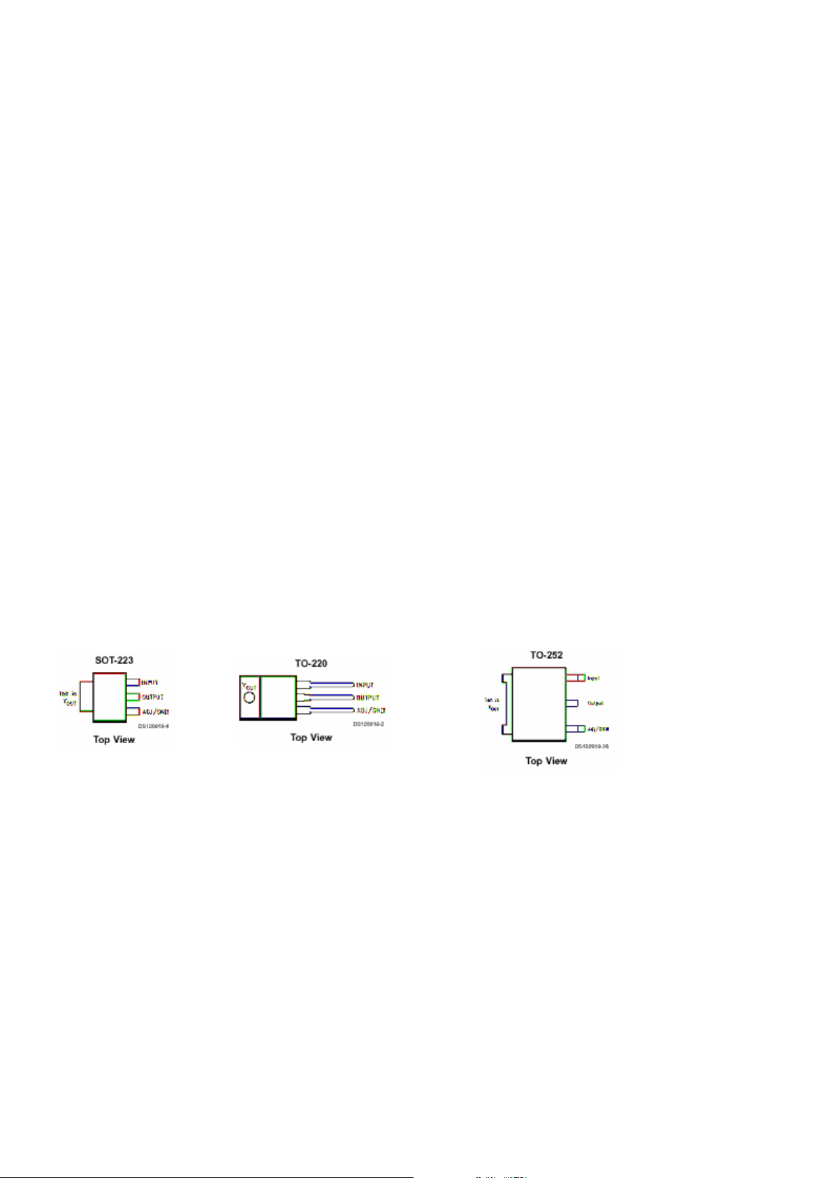
Connection Diagrams
Features
Applications
15.11. LM317
15.11.1. General Description
This monolithic integrated circuit is an adjustable 3-terminal positive voltage regulator designed to supply more
than 1.5A of load current with an output voltage adjustable over a 1.2 to 37V. It employs internal current limiting,
thermal shut-down and safe area compensation.
15.11.2.
• Output Current In Excess of 1.5A
• Output Adjustable Between 1.2V and 37V
• Internal Thermal Overload Protection
• Internal Short Circuit Current Limiting
• Output Transistor Safe Operating Area Compensation
• TO-220 Package
TFT TV Service Manual
Features
19
Page 24
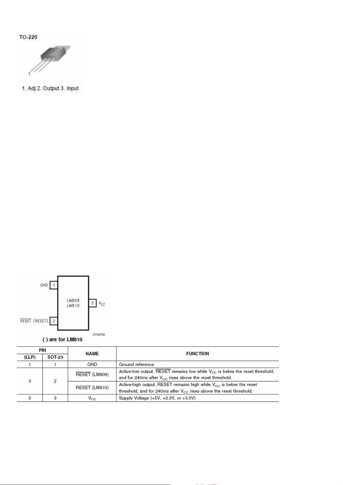
15.11.3.
Pin Description
15.12. LM809
15.12.1. General Description
The LM809/810 microprocessor supervisory circuits can be used to monitor the power supplies in microprocessor and
digital systems. They provide a reset to the microprocessor during power-up, power-down and brown-out conditions.
The function of the LM809/810 is to monitor the VCC supply voltage, and assert a reset signal whenever this voltage
declines below the factory-programmed reset threshold. The reset signal remains asserted for 240 ms after VCC rises
above the threshold. The LM809 has an active- low RESET output, while the LM810 has an active-high RESET output.
Seven standard reset voltage options are available, suitable for monitoring 5V, 3.3V, and 3V supply voltages. With a
low supply current of only 15μA, the LM809/810 are ideal for use in portable equipment.
15.12.2. Features
• Precise monitoring of 3V, 3.3V, and 5V supply voltages
• Superior upgrade to MAX809/810
• Fully specified overtemperature
• 140 ms min. Power-On Reset pulse width, 240 ms typical
Active-low RESET Output(LM809)
Active-high RESET Output(LM810)
• Guaranteed RESET Output valid for VCC1V
• Low Supply Current, 15μAtyp
• Power supply transient immunity
15.12.3. Pinning
15.13. MSP34X1G (MSP3411G)
Multistandard Sound Processor Family
TFT TV Service Manual
20
Page 25
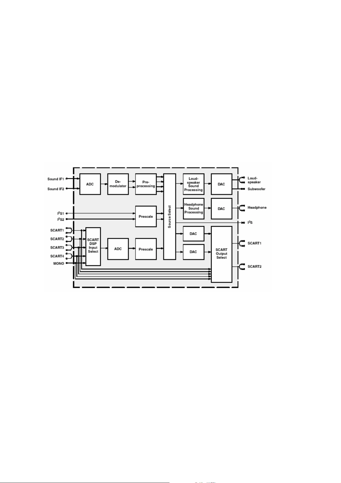
15.13.1.
Introduction
The MSP 34x1G family of single-chip Multistandard Sound Processors covers the sound processing of all
analog TV-Standards worldwide, as well as the NICAM digital sound standards. The full TV sound processing,
starting with analog sound IF signal-in, down to processed analog AF-out, is performed on a single chip. Figure
shows a simplified functional block diagram of the MSP 34x1G.
The MSP 34x1G has all functions of the MSP 34x0G with the addition of a virtual surround sound feature.
Surround sound can be reproduced to a certain extent with two loudspeakers. The MSP 34x1G includes the
Micronas virtualizer algorithm “3D-PANORAMA” which has been approved by the Dolby 1) Laboratories for with
the "Virtual Dolby Surround" technology. In addition, the MSP 34x1G includes the “PAN-ORAMA” algorithm.
These TV sound processing ICs include versions for processing the multichannel television sound ( MTS) signal conforming
to the standard recommended by the Broadcast Television Systems Committee (BTSC). The DBX noise reduction, or
alternatively, Micronas Noise Reduction (MNR) is performed alignment free.
Other processed standards are the Japanese FM-FM multiplex standard (EIA- J) and the FM Stereo Radio
standard.
Current ICs have to perform adjustment procedures in order to achieve good stereo separation for BTSC and
EIA-J. The MSP 34x1G has optimum stereo performance without any adjustments.
The MSP 34x1G has built-in automatic functions: The IC is able to detect the actual sound standard automatically (Automatic Standard Detection). Furthermore, pilot levels and identification signals can be evaluated
internally with subsequent switching between mono/stereo/bilingual; no I 2 C interaction is necessary (Automatic
Sound Selection).
Source Select
2
I
S bus interface consists of five pins:
1. I2S_DA_IN1, I2S_DA_IN2: For input, four channels (two channels per line, 2*16 bits) per sampling cycle (32
kHz) are transmitted.
2. I2S_DA_OUT: For output, two channels (2*16 bits) per sampling cycle (32 kHz) are transmitted.
3. I2S_CL: Gives the timing for the transmission of I
2
S serial data (1.024 MHz).
4. I2S_WS: The I2S_WS word strobe line defines the left and right sample.
15.13.2.
Features
• Standard Selection with single I2C transmission
• Automatic Standard Detection of terrestrial TV standards
• Automatic Sound Selection (mono/stereo/bilingual), new registers MODUS, STATUS
• Two selectable sound IF (SIF) inputs
• Automatic Carrier Mute function
• Interrupt output programmable (indicating status change)
• Loudspeaker / Headphone channel with volume, balance, bass, treble, loudness
• AVC: Automatic Volume Correction
• Subwoofer output with programmable low-pass and complementary high -pass filter
• 5-band graphic equalizer for loudspeaker channel
• Spatial effect for loudspeaker channel
• Four Stereo SCART (line) inputs, one Mono input; two Stereo SCART outputs
TFT TV Service Manual
21
Page 26
• Complete SCART in/out switching matrix
2
•TwoI
Sinputs;oneI2Soutput
• Dolby Pro Logic with DPL 351xA coprocessor
• All analog FM-Stereo A2 and satellite standards; AM-SECAM L standard
• S imultaneous demodulation of (very) high-deviation FM-Mono and NICAM
• Adaptive deemphasis for sat ellite (Wegener-Panda, acc. to ASTRA specification)
• ASTRA Digital Radio (ADR) together with DRP 3510A
• All NIC AM standards
• Korean FM-Stereo A2 standard
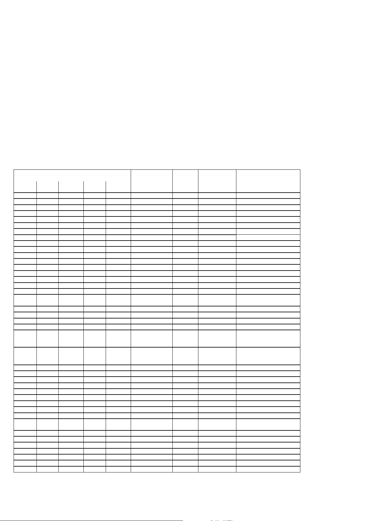
Pin connections
NC = not connected; leave vacant
LV = if not used, leave vacant
OBL = obligatory; connect as described in circuit diagram
DVSS: if not used, connect to DVSS
AHVSS: connect to AHVSS
Pin No. Pin Name Type
PLCC
68-pin
1 16 14 9 8 ADR_WS OUT LV ADR word strobe
2 - - - - NC LV Not connected
3 15 13 8 7 ADR_DA OUT LV ADR Data Output
4 14 12 7 6 I2S_DA_IN1 IN LV I2S1 data input
5 13 11 6 5 I2S_DA_OUT OUT LV I2S data output
6121054 I2S_WS IN/OUTLV I
7 11 9 4 3 I2S_CL IN/OUT LV I2Sclock
8 10 8 3 2 I2C_DA IN/OUT OBL I2C data
9 9 7 2 1 I2C_CL IN/OUT OBL I2Cclock
10 8 - 1 64 NC LV Not connected
11 7 6 80 63 STANDBYQ IN OBL Stand-by (low-active)
12 6 5 79 62 ADR_SEL IN OBL I2C bus address select
13 5 4 78 61 D_CTR_I/O_0 IN/OUT LV D_CTR_I/O_0
14 4 3 77 60 D_CTR_I/O_1 IN/OUT LV D_CTR_I/O_1
15 3 - 76 59 NC LV Not connected
16 2 - 75 58 NC LV Not connected
17 - - - - NC LV Not connected
18 1 2 74 57 AUD_CL_OUT OUT LV
19 64 1 73 56 TP LV Test pin
20 63 52 72 55 XTAL_OUT OUT OBL Crystal oscillator
21 62 51 71 54 XTAL_IN IN OBL Crystal oscillator
22 61 50 70 53 TESTEN IN OBL Test pin
23 60 49 69 52 ANA_IN2+ IN
24 59 48 68 51 ANA_IN - IN
25 58 47 67 50 ANA_IN1+ IN LV IF input 1
26 57 46 66 49 AVSUP OBL Analog power supply 5V
- - - 65 - AVSUP OBL Analog power supply 5V
- - - 64 - NC LV Not connected
- - - 63 - NC LV Not connected
27 56 45 62 48 AVSS OBL Analog ground
- - - 61 - AVSS OBL Analog ground
28 55 44 60 47 MONO_IN IN LV Mono input
- - - 59 - NC LV Not connected
29 54 43 58 46 VREFTOP OBL
30 53 42 57 45 SC1_IN_R IN LV SCART 1 input, right
31 52 41 56 44 SC1_IN_L IN LV SCART 1 input, left
32 51 - 55 43 ASG1 AHVSS Analog Shield Ground 1
33 50 40 54 42 SC2_IN_R IN LV SCART 2 input, right
34 49 39 53 41 SC2_IN_L IN LV SCART 2 input, left
35 48 - 52 40 ASG2 AHVSS Analog Shield Ground 2
36 47 38 51 39 SC3_IN_R IN LV SCART 3 input, right
PSDIP
64-pin
PSDIP
52-pin
PQFP
80-pin
PLQFP
64-pin
Connection
(if not used)
AVSS via
56 pF/LV
AVSS via
56 pF/LV
Short Description
2
S word strobe
Audio clock output
(18.432 MHz)
IF Input 2 (can be left
vacant, only if IF input 1 is
also not in use)
IFcommon(canbeleft
vacant, only if IF input 1 is
also not in use)
Reference voltage IF A/D
converter
TFT TV Service Manual
22
Page 27
37 46 37 50 38 SC3_IN_L IN LV SCART 3 input, left
38 45 - 49 37 ASG4 AHVSS Analog Shield Ground 4
39 44 - 48 36 SC4_IN_R IN LV SCART 4 input, right
40 43 - 47 35 SC4_IN_L IN LV SCART 4 input, left
41 - - 46 - NC LV or AHVSS Not connected
42 42 36 45 34 AGNDC OBL Analog reference voltage
43 41 35 44 33 AHVSS OBL Analog ground
- - - 43 - AHVSS OBL Analog ground
- - - 42 - NC LV Not connected
- - - 41 - NC LV Not connected
44 40 34 40 32 CAPL_M OBL Volume capacitor MAIN
45 39 33 39 31 AHVSUP OBL Analog power supply 8V
46 38 32 38 30 CAPL_A OBL Volume capacitor AUX
47 37 31 37 29 SC1_OUT_L OUT LV SCART output 1, left
48 36 30 36 28 SC1_OUT_R OUT LV SCART output 1, right
49 35 29 35 27 VREF1 OBL Reference ground 1
50 34 28 34 26 SC2_OUT_L OUT LV SCART output 2, left
51 33 27 33 25 SC2_OUT_R OUT LV SCART output 2, right
52 - - 32 - NC LV Not connected
53 32 - 31 24 NC LV Not connected
54 31 26 30 23 DACM_SUB OUT LV Subwoofer output
55 30 - 29 22 NC LV Not connected
56 29 25 28 21 DACM_L OUT LV Loudspeaker out, left
57 28 24 27 20 DACM_R OUT LV Loudspeaker out, right
58 27 23 26 19 VREF2 OBL Reference ground 2
59 26 22 25 18 DACA_L OUT LV Headphone out, left
60 25 21 24 17 DACA_R OUT LV Headphone out, right
- - - 23 - NC LV Not connected
- - - 22 - NC LV Not connected
61 24 20 21 16 RESETQ IN OBL Power-on-reset
62 23 - 20 15 NC LV Not connected
63 22 - 19 14 NC LV Not connected
64 21 19 18 13 NC LV Not connected
65 20 18 17 12 I2S_DA_IN2 IN LV I2S2-data input
66 19 17 16 11 DVSS OBL Digital ground
- - - 15 - DVSS OBL Digital ground
- - - 14 - DVSS OBL Digital ground
67 18 16 13 10 DVSUP OBL Digital power supply 5V
- - - 12 - DVSUP OBL Digital power supply 5V
- - - 11 - DVSUP OBL Digital power supply 5V
68 17 15 10 9 ADR_CL OUT LV ADR clock
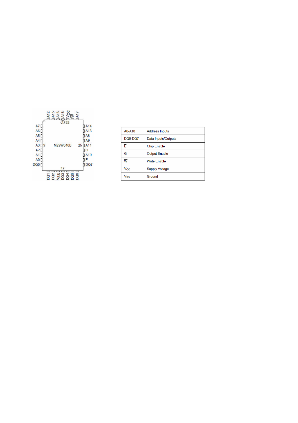
15.14. M29W040B
15.14.1. Description
The M29W040B is a 4 Mbit (512Kb x8) non-volatile memory that can be read, erased and reprogrammed. These operations
can be performed using a single low voltage (2.7 to 3.6V) supply. On power-up the memory defaults to its Read mode
where it can be read in the same way as a ROM or EPROM. The M29W040B is fully backward compatible with the
M29W040.The memory is divided into blocks that can be erased independently so it is possible to preserve valid data while
old data is erased. Each block can be protected independently to prevent accidental Program or Erase commands from
modifying the memory. Program and Erase commands are writ-ten to the Command Interface of the memory. An on-chip
Program/Erase Controller simplifies the p rocess of programming or erasing the memory by taki ng care of all of the special
operations that are required to update the memory contents. The end of a program or erase operation can be detected and
any error conditions identified. The command set required to control the memory is consistent with JEDEC standards. Chip
Enable, Output Enable and Write Enable signals control the bus operation o f the memory. They allow simple connection to
most microprocessors, often without additional logic.
15.14.2.
• SINGLE 2.7 to 3.6V SUPPLY VOLTAGE for PROGRAM, ERASE and READ OPERATIONS
• ACCESS TIME: 55ns
• PROGRAMMING TIME
- 10μs per Byte typical8
• UNIFORM 64 Kbytes MEMORY BLOCKS
• PROGRAM/ERASE CONTROLLER
- Embedded Byte Program algorithm
- Embedded Multi-Block/Chip Erase algorithm
- Status Register Polling and Toggle Bits
Features
TFT TV Service Manual
23
Page 28
• ERASE SUSPEND and RESUME MODES
- Read and Program another Block during Erase Suspend
• UNLOCK BYPASS PROGRAM COMMAND
- Faster Production/Batch Programming
• LOW POWER CONSUMPTION
- Standby and Automatic Standby
• 100,000 PROGRAM/ERASE CYCLES per BLOCK
• 20 YEARS DATA RETENTION
- Defectivity below 1 ppm/year
• ELECTRONIC SIGNATURE
- Manufacturer Code: 20h
- Device Code: E3h
15.14.3.
Pin Descriptions
15.15. MC33202
15.15.1. General Description
The MC33201/2/4 family of operational amplifiers provide railítoírail operation on both the input and output.
The inputs can be driven as high as 200mV beyond the supply rails without phase reversal on the outputs, and
the output can swing within 50 mV of each rail. This railítoírail operation enables the user to make full use of
the supply voltage range available. It is designed to work at very low supply voltages (±0.9 V) yet can operate
with a supply of up to +12V and ground. Output current boosting techniques provide a high output current
capability while keeping the drain current of the amplifier to a minimum. Also, the combination of low noise and
distortion with a high slew rate and drive capability make this an ideal amplifier for audio applications.
15.15.2.
• Low Voltage, Single Supply Operation (+1.8 V and Ground to +12 V and Ground)
• Input Voltage Range Includes both Supply Rails
• Output Voltage Swings within 50 mV of both Rails
• No Phase Reversal on the Output for Overídriven Input Signals
• High Output Current (ISC = 80 mA, Typ)
• Low Supply Current (ID = 0.9 mA, Typ)
• 600 Output Drive Capability
• Extended Operating Temperature Ranges (í40° to +105°C and í55° to +125°C)
• Typical Gain Bandwidth Product = 2.2 MHz
•PbíFree Packages are Available
TFT TV Service Manual
Features
24
Page 29
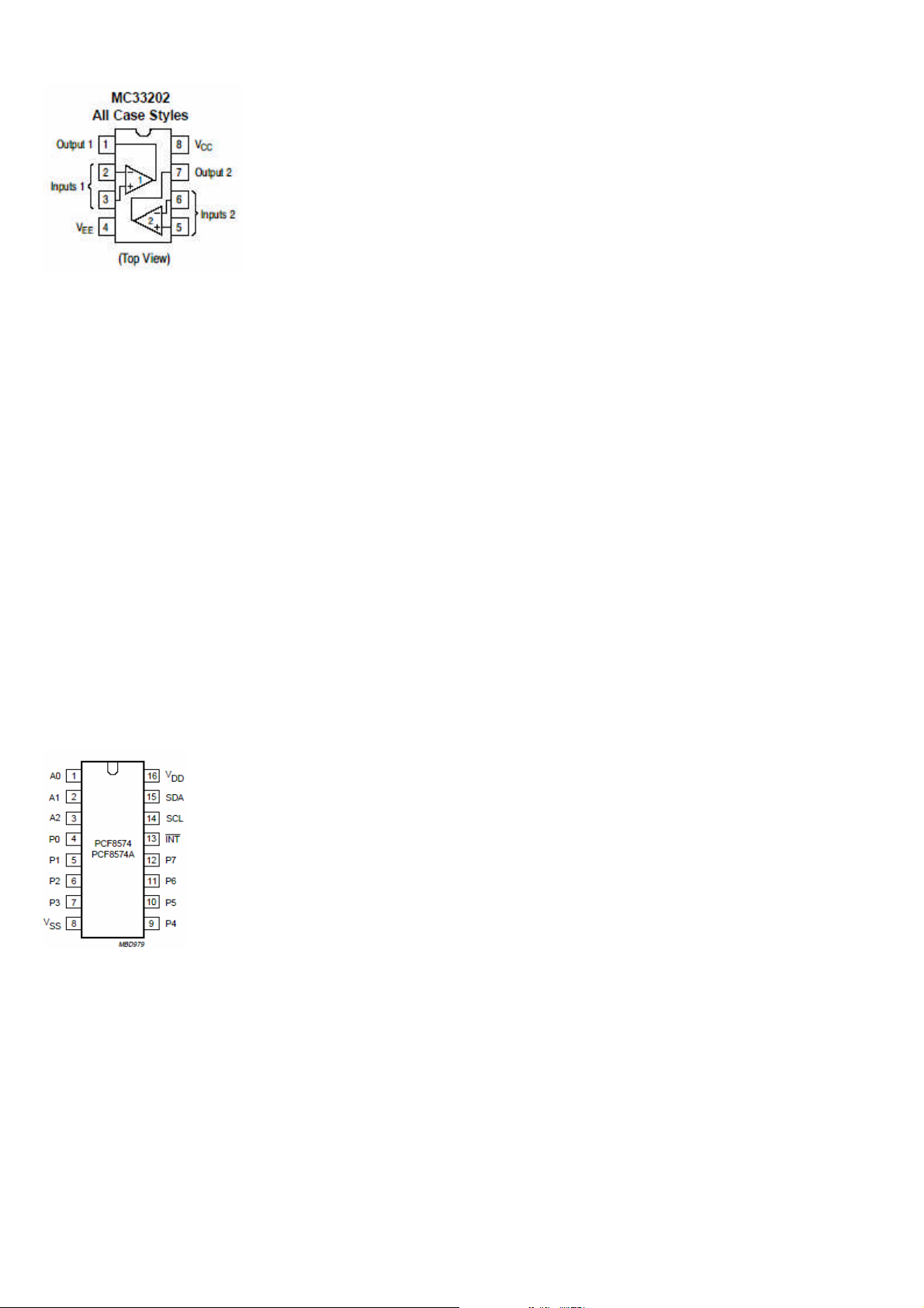
15.15.3.
Pin Connections
15.16. PCF8574
15.16.1. General Description
The P CF8574 is a silicon CMOS circuit. It provides general purpose remote I/O expansion for most microcontroller
families via the two-line bidirectional bus (I
interface. T he PCF8574 has a low current consumption and includes latched outputs with high current drive capabilit y for
directly driving LEDs. It also possesses an interrupt line (INT) which can be connected to the interrupt logic of the
microcontroller. By sending an interrupt signal on this line, the remote I/O can inform the microcontroller if there is
incoming data on its ports without having to communicate via the I
simple slave device.
2
C).The device consists of an 8-bit quasi-bidirectional port and an I2C-bus
2
C-bus. T his means that the PCF8574 can remain a
15.16.2.
Features
• Operating supply voltage 2.5 to 6V
• Low standby current consumption of 10 μA maximum
2
•I
C to parallel port expander
• Open-drain interrupt output
• 8-bit remote I/O port for the I
2
C-bus
• Compatible with most microcontrollers
• Latched outputs with high current drive capability for directly driving LEDs
• Address by 3 hardware address pins for use of up to 8 devices (up to 16 with PCF8574A)
• DIP16, or space-saving SO16 or SSOP20 packages.
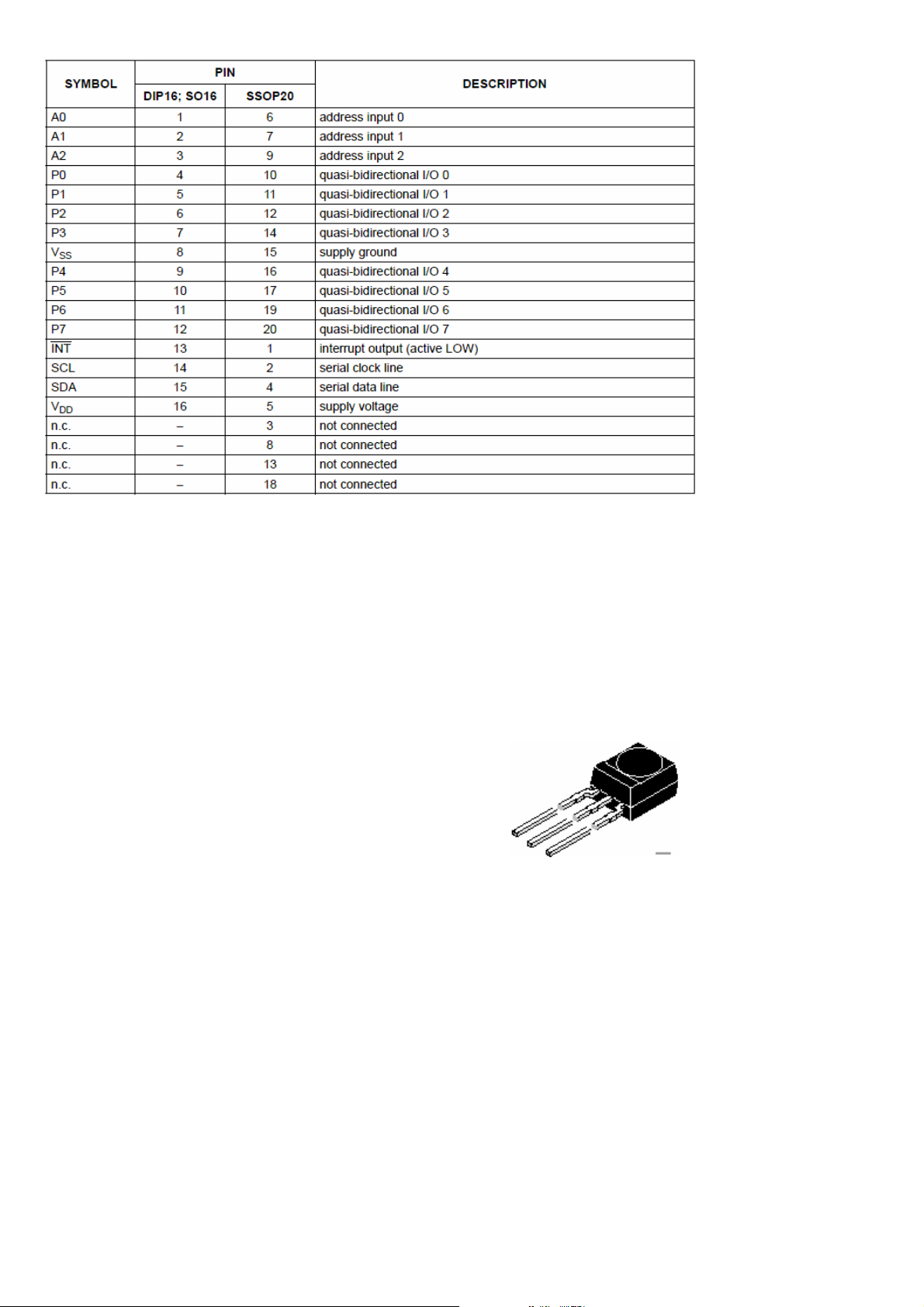
15.16.3.
Pinning
TFT TV Service Manual
25
Page 30
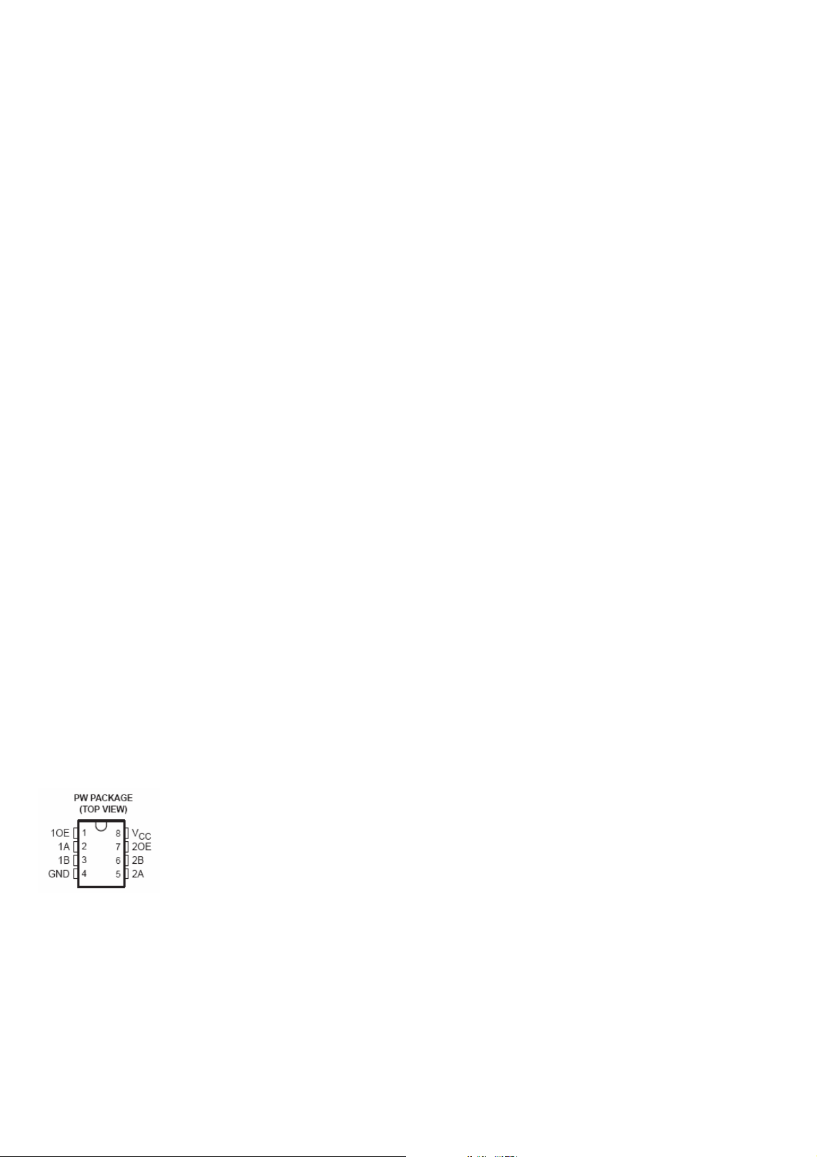
15.17. TSOP1836
15.17.1. Description
The TSOP18.– series are miniaturized receivers for infrared remote control systems. PIN diode and preamplifier
are assembled on lead frame, the epoxy package is designed as IR filter. Carrier frequency for TSOP1836 is 36
kHz.
The demodulated output signal can directly be decoded by a microprocessor. The main benefit is the reliable
function even in disturbed ambient and the protection against uncontrolled output pulses.
15.17.2.
• Photo detector and preamplifier in one package
• Internal filter for PCM frequency
• TTL and CMOS compatibility
• Output active low
• Improved shielding against electrical field disturbance
• Suitable burst length .6 cycles/burst
Special Features
• Small size package
• Enhanced immunity against all kinds of disturbance light
• No occurrence of disturbance pulses at the output
• Short settling time after power on (<200_s)
Features
15.18. PI5V330
15.18.1. General Description
The PI5V330 is well suited for video applications when switching composite or RGB analogue. A picture-inpicture application will be described in this brief. The pixel-rate creates video overlays so two or more pictures
can be viewed at the same time. An inexpensive NTSC titler can be implemented by superimposing the output
of a character generator on a standard composite video background.
TFT TV Service Manual
26
Page 31

15.19. SDA55XX (SDA5550)
15.19.1. General description
The SDA55XX is a single chip teletext decoder for decoding World System Teletext data as well as Video
Programming System (VPS), Program Delivery Control (PDC), and Wide Screen Signalling (WSS) data used for
PAL plus transmissions (Line 23). The device also supports Closed caption acquisition and decoding. The
device provides an integrated general-purpose, fully 8051-compatible Microcontroller with television specific
hardware features. Microcontroller has been enhanced to provide powerful features such as memory banking,
data pointers, and additional interrupts etc. The on-chip display unit for displaying Level 1.5 teletext data can
also be used for customer defined on screen displays. Internal XRAM consists of up to16 Kbytes. Device has an
internal ROM of up to 128 KBytes. ROMless versions can access up to 1 MByte of external RAM and ROM. The
SDA 55XX supports a wide range of standards including PAL, NTSC and contains a digital slicer for VPS, WSS,
PDC, TTX and Closed Caption, an accelerating acquisition hardware module, a display generator for Level 1.5
TTX data and powerful On screen Display capabilities based on parallel attributes, and Pixel oriented characters
(DRCS).
The 8-bit Microcontroller runs at 360 ns. cycle time (min.). Controller with dedicated hardware does most of the
internal TTX acquisition processing, transfers data to/from external memory interface and receives/ transmits
data via I
buffer of 1 Kilobyte. The Microcontroller firmware performs all the acquisition tasks (hamming and parity-checks,
page search and evaluation of header control bits) once per field. Additionally, the firmware can provide highend Teletext features like Packet-26-handling, FLOF, TOP and list-pages. The interface to user software is
optimized for minimal overhead. SDA 55XX is realized in 0.25 micron technology with 2.5 V supply voltage and
3.3 V I/O (TTL compatible). The software and hardware development environment (TEAM) is available to
simplify and speed up the development of the software and On Screen Display. TEAM stands for TVT Expert
Application Maker. It improves the TV controller software quality in following aspects:
– Shorter time to market
– Re-usability
– Target independent development
– Verification and validation before targeting
– General test concept
– Graphical interface design requiring minimum programming and controller know how.
– Modular and open tool chain, configurable by customer.
2
C-firmware user-interface. The slicer combined with dedicated hardware stores TTX data in a VBI
15.20. SIL 9993
15.20.1. General Description
The SiI 9993 is the first generation of PanelLink receivers that are designed for the HDMI 1.0 (High Definition Multimedia
Interface) specification. DTVs, plasma displa ys, LCD TVs and projectors can now provide the purest level of protected
digital audio/video over a simple, low cost cable. Backwards compatibility with DVI 1.0 allows HDMI systems to connect
to any DVI 1.0 host (DVD players, HD set top boxes, D-VHS players and receivers, PC). The SiI 9993 incorporates a
flexible audio and video interface. The receiver can connect to RGB input and output YCbCr using an integrated color
space converter. This allows full backward compatibility to DVI, and interfaces to all major video processors. A S/PDIF
port can output PCM encoded data as well as Dolby Digital, DTS and all other formats capable of being sent over S/PDIF.
A 2-channel I2S port outputs data converted from S/PDIF. The SiI 9993 comes pre -programmed with HDCP keys, greatly
simplifying the manufacturing process, lowering costs, all the while providing the highest level of HDCP key security.
Silicon Image’s PanelLink receivers use the latest generation of PanelLink TMDS core technology. These PanelLink cores
pass all HDMI compliancy tests.
15.20.2.
• HDMI 1.0 and DVI 1.0 compliant receiver
• Integrated PanelLink core supports DTV resolutions (480i/576i/480p/576p/720p/1080i)
• Digital video interface supports video processors:
o 24-bit RGB 4:4:4
o 24-bit YCbCr 4:4:4
o 16/20/24-bit YCbCr 4:2:2
o 8/10/12-bit YCbCr 4:2:2 embedded syncs
• Analog RGB and YPbPr output:
o10-bitDAC
o Separate or Composite Syncs (Sync on G)
Features
TFT TV Service Manual
27
Page 32
• S/PDIF output supports PCM, Dolby Digital, DTS digital audio transmission (32-48kHz Fs) using IEC 60958
and IEC 61937.
• Programmable I
2
S interface for connection to low-cost audio DACs.
• Integrated HDCP decryption engine for receiving protected audio and video content
• Pre-programmed HDCP keys provide highest level of key security, simplifies manufacturing
• Programmable registers via slave I
2
C interface
• 3.3V operation in 100-pin TQFP package
• Flexible power management
15.21. SN74CB3Q3305
15.21.1. General Description
The SN74CB3Q3305 is a high-bandwidth FET bus switch utilizing a charge pump to elevate the gate voltage of
the pass transistor, providing a low and flat ON-state resistance (r
allows for minimal propagation delay and supports rail-to-rail switching on the data input/output (I/O) ports. The
device also features low data I/O capacitance to minimize capacitive loading and signal distortion on the data
bus. Specifically designed to support high-bandwidth applications, the SN74CB3Q3305 provides an optimized
interface solution ideally suited for broadband communications, networking, and data-intensive computing
systems.
). The low and flat ON-state resistance
on
15.21.2.
Features
• High-Bandwidth Data Path (Up To 500 MHz)
• 5-V Tolerant I/Os with Device Powered-Up or Powered-Down
• Low and Flat ON-State Resistance (r
) Characteristics Over Operating Range (ron=37\SLFDO
on
• Rail-to-Rail Switching on Data I/O Ports
í 0- to 5-V Switching With 3.3-V VCC
í 0- to 3.3-V Switching With 2.5-V VCC
• Bidirectional Data Flow, With Near-Zero Propagation Delay
• Low Input/Output Capacitance Minimizes Loading and Signal Distortion (C
• Fast Switching Frequency (f
= 20 MHz Max)
OE
=3.5pFTypical)
io(OFF)
• Data and Control Inputs Provide Undershoot Clamp Diodes
• Low Power Consumption (ICC = 0.25 mA Typical)
• VCC Operating Range From 2.3 V to 3.6 V
• Data I/Os Support 0 to 5-V Signaling Levels (0.8- V, 1.2-V, 1.5-V, 1.8-V, 2.5-V, 3.3-V, 5-V)
• Control Inputs Can be Driven by TTL or 5-V/3.3-V CMOS Outputs
•I
Supports Partial-Power-Down Mode Operation
off
• Latch-Up Performance Exceeds 100 mA PerJESD 78, Class II
• ESD Performance Tested Per JESD 22
í 2000-V Human-Body Model (A114-B, Class II)
í 1000-V Charged-Device Model (C101)
• Supports Both Digital and Analog Applications: USB Interface, Differential Signal Interface, Bus Isolation, Low-
Distortion Signal Gating
15.21.3.
Pin Connections
15.22. ST24LC21
15.22.1. Description
The ST24LC21 is a 1K bit electrically erasable programmable memory (EEPROM), organized by 8 bits. This
device can operate in two modes: Transmit Only mode and I
in Transmit Only mode with EEPROM data clocked out from the rising edge of the signal applied on VCLK. The
devicewillswitchtotheI
2
C bidirectional mode upon the falling edge of the signal applied on SCL pin. The
TFT TV Service Manual
2
C bidirectional mode. When powered, the device is
28
Page 33
ST24LC21 can not switch from the I
2
C bidirectional mode to the Transmit Only mode (except when the power
supply is removed). The device operates with a power supply value as low as 2.5V. Both Plastic Dual-in-Line
and Plastic Small Outline packages are available.
15.22.2.
Features
• 1 million Erase/Write cycles
• 40 years data retention
• 2.5V to 5.5V single supply voltage
• 400k Hz compatibility over the full range of supply voltage
• Two wire serial interface I
2
C bus compatible
• Page Write (Up To 8 Bytes)
• Byte, random and sequential read modes
• Self timed programming cycle
• Automatic address incrementing
• Enhanced ESD/Latch up
• Performances
15.22.3.
Pin connections
DIP Pin connections CO Pin connections
NC: Not connected
Signal names
SDA Serial data Address Input/Output
SCL Serial Clock (I2C mode)
Vcc Supply voltage
V
ss
VCLK Clock transmit only mode
Ground
15.23. LM2576
15.23.1. General Description
The LM2576 series of regulators are monolithic integrated circuits ideally suited for easy and convenient design of a step–
down switching regulator (buck converter). All circuits of this series are capable of driving a 3.0 A load with excellent line
and load regulation.
These devices are available in fixed output voltages of 3.3 V, 5.0 V, 12 V, 15 V, and an adjustable output
version. These regulators were designed to minimize the number of external components to simplify the power
supply design. Standard series of inductors optimized for use with the LM2576 are offered by several different
inductor manufacturers.
Since the LM2576 converter is a switch–mode power supply, its efficiency is significantly higher in comparison
with popular three–terminal linear regulators, especially with higher input voltages. In many cases, the power
dissipated is so low that no heatsink is required or its size could be reduced dramatically.
A standard series of inductors optimized for use with the LM2576 are available from several different
manufacturers. This feature greatly simplifies the design of switch–mode power supplies.
The LM2576 features include a guaranteed ±4% tolerance on output voltage within specified input voltages and
output load conditions, and ±10% on the oscillator frequency (±2% over 0°C to 125°C). External shutdown is
included, featuring 80 mA (typical) standby current. The output switch includes cycle–by–cycle current limiting,
as well as thermal shutdown for full protection under fault conditions.
15.23.2.
Features
• 3.3 V, 5.0 V, 12 V, 15 V, and Adjustable Output Versions
TFT TV Service Manual
29
Page 34
• Adjustable Version Output Voltage Range, 1.23 to 37 V ±4% Maximum Over Line and Load Conditions
• Guaranteed 3.0 A Output Current
• Wide Input Voltage Range
• Requires Only 4 External Components
• 52 kHz Fixed Frequency Internal Oscillator
• TTL Shutdown Capability, Low Power Standby Mode
• High Efficiency
• Uses Readily Available Standard Inductors
• Thermal Shutdown and Current Limit Protection
• Moisture Sensitivity Level (MSL) Equals 1
15.23.3.
Pin description
15.24. MC34063
15.24.1. Description
The MC34063A Series is a monolithic control circuit containing the primary functions required for DC–to–DC converters.
These devices consist of a n int ernal te mperature co mpensated reference, comparator, controlled duty cycle oscillator with
an active current limit circuit, driver and high current output switch. This series was specifically designed to be
incorporated in Step–Down and Step–Up an d Voltage–Inverting applications with a minimum number of external
components.
15.24.2.
• Operation from 3.0 V to 40 V Input
• Low Standby Current
• Current Limiting
• Output Switch Current to 1.5 A
• Output Voltage Adjustable
• Frequency Operation to 100 kHz
• Precision 2% Reference
Features
15.24.3.
TFT TV Service Manual
Pin connections
30
Page 35
15.25. TDA1308
15.25.1. General Description
The TDA1308 is an integrated class AB stereo headphone driver contained in an SO8 or a DIP8 plastic
package. The device is fabricated in a 1 mm CMOS process and has been primarily developed for portable
digital audio applications.
15.25.2.
Features
• Wide temperature range
• No switch ON/OFF clicks
• Excellent power supply ripple rejection
• Low power consumption
• Short-circuit resistant
• High performance
• high signal-to- noise ratio
• High slew rate
• Low distortion
• Large output voltage swing.
15.25.3. Pinning
SYMBOL PIN DESCRIPTION PIN VALUE
OUTA 1 Output A (Voltage swing) Min : 0.75V, Max : 4.25V
INA(neg) 2 Inverting input A Vo(clip) : Min : 1400mVrms
INA(pos) 3 Non-inverting input A 2.5V
V
SS
INB(pos) 5 Non-inverting input B 2.5V
INB(neg) 6 Inverting input B Vo(clip) : Min : 1400mVrms
OUTB 7 Output B (Voltage swing) Min : 0.75V, Max : 4.25V
V
DD
4 Negative supply 0V
8 Positive supply 5V, Min : 3.0V, Max : 7.0V
15.26. TDA9886
15.26.1. General Description
The TDA9886 is an alignment-free single standard (without positive modulation) vision and sound IF signal PLL.
15.26.2.
• 5 V supply voltage
• Gain controlled wide-band Vision Intermediate Frequency (VIF) amplifier (AC-coupled)
• Multistandard true synchronous demodulation with active carrier regeneration (very linear demodulation, good
intermodulation figures, reduced harmonics, excellent pulse response)
• Gated phase detector for L/L accent standard
• Fully integrated VIF Voltage Controlled Oscillator (VCO), alignment -free; frequencies switchable for all negative and
positive modulated standards via I
• Digital acquisition help, VIF frequencies of 33.4, 33.9, 38.0, 38.9, 45.75 and 58.75 MHz
• 4 MHz reference frequency input [signal from Phase-Locked Loop (PLL) tuning system] or operating as crystal
oscillator
• VIF Automatic Gain Control (AGC) detector for gain control, operating as peak sync detector for negative modulated
signals and as a peak white detector for positive modulated signals
• Precise fully digital Automatic Frequency Control (AFC) detector with 4-bit digital-to-analogue converter; AFC bits via
2
C -bus readable
I
• TakeOver Point (TOP) adjustable via I
• Fully integrated sound carrier trap for 4.5, 5.5, 6.0 and 6.5 MHz, controlled by FM-PLL oscillator
• Sound IF (SIF) input for single reference Quasi Split Sound (QSS) mode (PLL controlled)
• SIF AGC for gain controlled SIF amplifier; single reference QSS mixer able to operate in high performance single
reference QSS mode and in intercarrier mode, switchable via I
Features
2
C-bus
2
C-bus or alternatively with potentiometer
2
C-bus
TFT TV Service Manual
31
Page 36
•
AM demodulator without extra reference circuit
• Alignment-free selective FM- PLL demodulator with high linearity and low noise
2
• I
C-bus control for all functions
2
• I
C-bus transceiver with pin programmable Module Address (MAD).
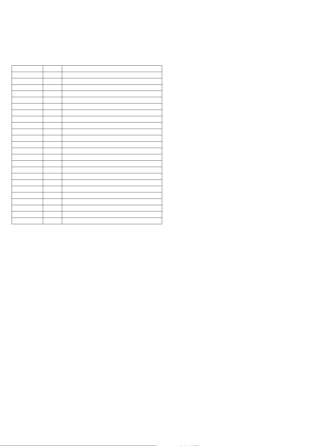
15.26.3. Pinning
SYMBOL PIN DESCRIPTION
VIF1 1 VIF differential input 1
VIF2 2 VIF differential input 2
OP1 3 output 1 (open-collector)
FMPLL 4 FM-PLL for loop filter
DEEM 5 de-emphasis output for capacitor
AFD 6 AF decoupling input for capacitor
DGND 7 digital ground
AUD 8 audio output
TOP 9 tuner AGC TakeOver Point (TOP)
SDA 10 I2C-bus data input/output
SCL 11 I2C-bus clock input
SIOMA 12 sound intercarrier output and MAD select
n.c. 13 not connected
TAGC 14 tuner AGC output
REF 15 4 MHz crystal or reference input
VAGC 16 VIF-AGC for capacitor; note 1
CVBS 17 video output
AGND 18 analog ground
VPLL 19 VIF-PLL for loop filter
V
P
AFC 21 AFC output
OP2 22 output 2 (open-collector)
SIF1 23 SIF differential input 1
SIF2 24 SIF differential input 2
20 supply voltage (+5 V)
15.27. TPA3004D2
15.27.1. General Description
The TPA3004D2 is a 12-W (per channel) efficient, Class-D audio amplifier for driving bridged-tied stereo speakers. The
TPA3004D2 can drive stereo speakers as low as 4 7KHKLJKHIILFLHQF\RIWKH73$'HOLPLQDWHVWKHQHHGIRU
external heatsinks when playing music.
Stereo speaker volume is controlled with a dc voltage applied to the volume control terminal offering a range of gain from –
40 dB to 36 dB. Line outputs, for driving external headphone amplifier inputs, are also dc voltage controlled with a range
ofgainfrom–56dBto20dB.
An integrated 5-V regulated supply is provided for powering an external headphone amplifier.
15.27.2.
• 12-W/Ch Into an 8-/RDG)URP -V Supply
• Efficient, Class-D Operation Eliminates Heatsinks and Reduces Power Supply Requirements
• 32-Step DC Volume Control From í40 dB to 36 dB
• Line Outputs For External Headphone Amplifier With Volume Control
• Regulated 5-V Supply Output for Powering TPA6110A2
• Space-Saving, Thermally-Enhanced PowerPAD
• Thermal and Short-Circuit Protection.
Features
TM
Packaging
TFT TV Service Manual
32
Page 37
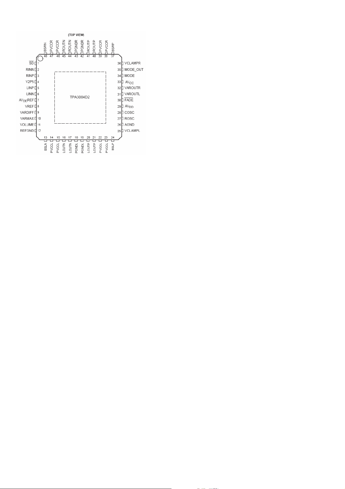
15.27.3.
Pinning
TFT TV Service Manual
33
Page 38
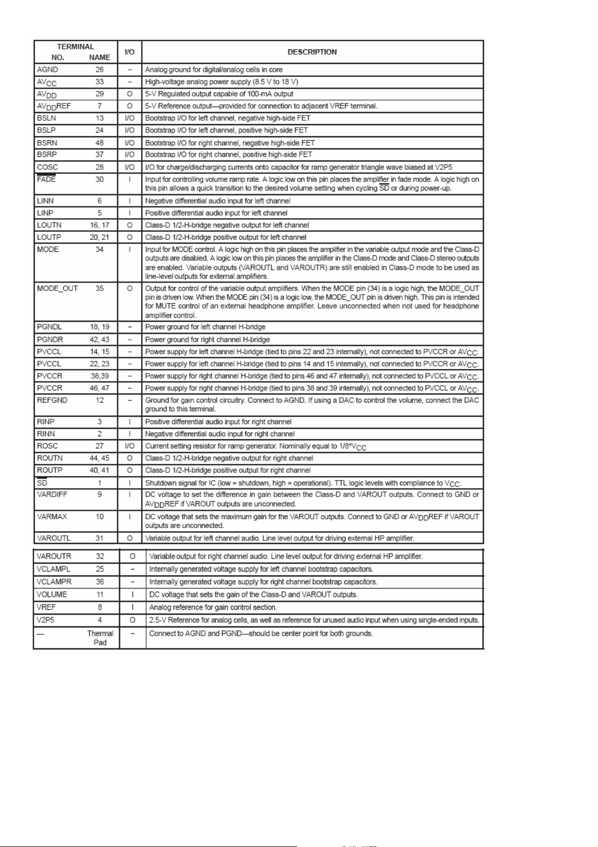
15.28.
15.29. μPA672T
15.29.1. General Description
The μPA672T is a super-mini-mold device provided with two MOS FET elements. It achieves high-density
mounting and saves mounting costs.
TFT TV Service Manual
34
Page 39
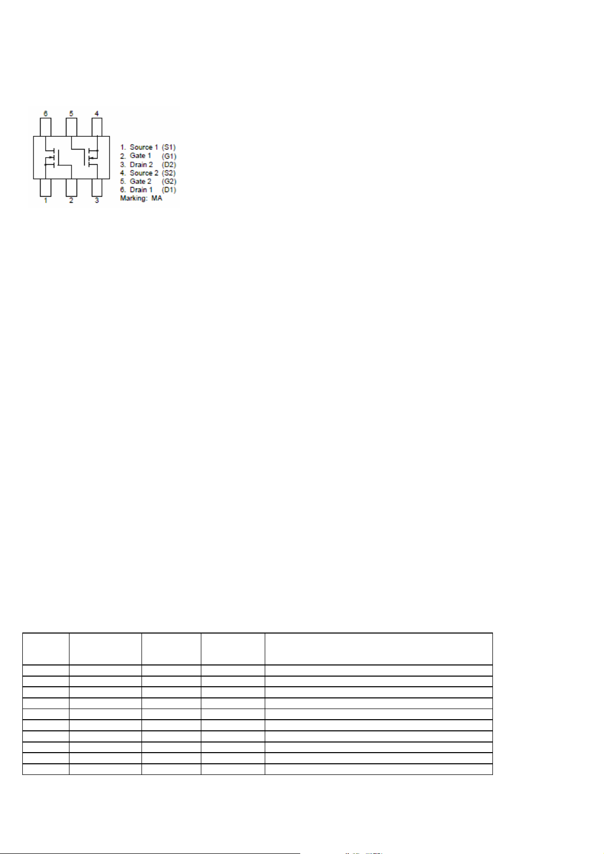
15.29.2.
Features
• Two MOS FET circuits in package the same size as SC-70
• Automatic mounting supported
15.29.3. Pin Connection
15.30. VPC3230D
15.30.1. General Description
The VPC 323xD is a high-quality, single-chip video front-end, which is targeted for 4:3 and 16:9, 50/60-Hz and
100/120 Hz TV sets. It can be combined with other members of the DIGIT3000 IC family (such as DDP 331x)
and/or it can be used with 3rd-party products.
The main features of the VPC 323xD are
• high-performance adaptive 4H comb filter Y/C separator with adjustable vertical peaking
• multi-standard colour decoder PAL/NTSC/SECAM including all substandards
• four CVBS, one S-VHS input, one CVBS output
• two RGB/YC
• integrated high-quality A/D converters and associated clamp and AGC circuits
• multi-standard sync processing
• linear horizontal scaling (0.25 ... 4), as well as non-linear horizontal scaling ‘Panorama-vision’
• PAL+ preprocessing
• line-locked clock, data and sync, or 656-output interface
• peaking, contrast, brightness, color saturation and tint for RGB/ YC
• high-quality soft mixer controlled by Fast Blank
• PIP processing for four picture sizes (1/4, 1/9, 1/16 or 1/36 of normal size) with 8-bit resolution
• 15 predefined PIP display configurations and expert mode (fully programmable)
• control interface for external field memory
2
•I
C-bus interface
r Cb component inputs, one Fast Blank (FB) input
r C b and CVBS/ S-VHS
• one 20.25-MHz crystal, few external components
• 80-pin PQFP package
15.30.2.
NC = not connected
LV = if not used, leave vacant
X = obligatory; connect as described in circuit diagram
SUPPLYA = 4.75...5.25 V, SUPPLYD = 3.15...3.45 V
Pin No.
PQFP
80-pin
1 B1/CB1IN IN VREF Blue1/Cb1 Analog Component Input
2 G1/Y1IN IN VREF Green1/Y1 Analog Component Input
3 R1/CR1IN IN VREF Read1/Cr1 Analog Component Input
4 B2/CB2IN IN VREF Blue2/Cb2 Analog Component Input
5 G2/Y2IN IN VREF Green2/Y2 Analog Component Input
6 R2/CR2IN IN VREF Read2/Cr2 Analog Component Input
7 ASGF X Analog Shield GND
8 FFRSTWIN IN LVorGNDDFIFO Reset Write Input
9V
10 V
Pin Name Type Connection
Pin Connections and Short Descriptions
Short Description
(if not used)
SUPCAP
SUPD
OUT X Digital Decoupling Circuitry Supply Voltage
SUPPLYD X Supply Voltage, Digital Circuitry
F
TFT TV Service Manual
35
Page 40
11 GND
12 GND
D
CAP
SUPPLYD X Ground, Digital Circuitry
OUT X Digital Decoupling Circuitry GND
13 SCL IN/OUT X I2C Bus Clock
14 SDA IN/OUT X I2CBusData
15 RESQ IN X Reset Input, Active Low
16 TEST IN GND
17 VGAV IN GND
18 YCOEQ IN GND
D
D
D
Test Pin, connect to GND
D
VGAV Input
Y/C Output Enable Input, Active Low
19 FFIE OUT LV FIFO Input Enable
20 FFWE OUT LV FIFO Write Enable
21 FFRSTW OUT LV FIFO Reset Write/Read
22 FFRE OUT LV FIFO Read Enable
23 FFOE OUT LV FIFO Output Enable
24 CLK20 IN/OUT LV Main Clock output 20.25 MHz
25 GND
26 V
SUPPA
PA
OUT X Pad Decoupling Circuitry GND
OUT X Pad Decoupling Circuitry Supply Voltage
27 LLC2 OUT LV Double Clock Output
28 LLC1 IN/OUT LV Clock Output
29 V
SUPLLC
SUPPLYD X Supply Voltage, LLC Circuitry
30 GNDLLC SUPPLYD X Ground, LLC Circuitry
31 Y7 OUT GND
32 Y6 OUT GND
33 Y5 OUT GND
34 Y4 OUT GND
35 GND
36 V
SUPY
Y
SUPPLYD X Ground, Luma Output Circuitry
SUPPLYD X Supply Voltage, Luma Output Circuitry
37 Y3 OUT GND
38 Y2 OUT GND
39 Y1 OUT GND
40 Y0 OUT GND
41 C7 OUT GND
42 C6 OUT GND
Y
Y
Y
Y
Y
Y
Y
Y
C
C
Picture Bus Luma (MSB)
Picture Bus Luma
Picture Bus Luma
Picture Bus Luma
Picture Bus Luma
Picture Bus Luma
Picture Bus Luma
Picture Bus Luma (LSB)
Picture Bus Chroma (MSB)
Picture Bus Chroma
43 C5 OUT GNDC Picture Bus Chroma
44 C4 OUT GND
45 V
SUPC
46 GND
C
SUPPLYD X Supply Voltage, Chroma Output Circuitry
SUPPLYD X Ground, Chroma Output Circuitry
47 C3 OUT GND
48 C2 OUT GND
49 C1 OUT GND
50 C0 OUT GND
51 GND
52 V
SUPSY
SY
SUPPLYD X Ground Sync Pad Circuitry
SUPPLYD X Supply Voltage, Sync Pad Circuitry
C
C
C
C
C
Picture Bus Chroma
Picture Bus Chroma
Picture Bus Chroma
Picture Bus Chroma
Picture Bus Chroma (LSB)
53 INTLC OUT LV Interlace Output
54 AVO OUT LV Active Video Output
55 FSY/HC/HSYA OUT LV Front Sync/ Horizontal Clamp Pulse/Front-End
Horizontal Sync Output
56 MSY/HS IN/OUT LV Main Sync/Horizontal Sync Pulse
57 VS OUT LV Vertical Sync Pulse
58 FPDAT/VSYA IN/OUT LV Front End/Back-End Data/Front-End Vertical Sync
Output
59 V
STBYY
SUPPLYA X Standby Supply Voltage
60 CLK5 OUT LV CCU 5 MHz Clock Output
61 NC - LVorGNDD Not Connected
62 XTAL1 IN X Analog Crystal Input
63 XTAL2 OUT X Analog Crystal Output
64 ASGF X Analog Shield GND
65 GND
F
SUPPLYA X Ground, Analog Front-End
F
66 VRT OUTPUT X Reference Voltage Top, Analog
67 I2CSEL IN X I2C Bus Address Select
68 ISGND SUPPLYA X Signal Ground for Analog Input, connect to GND
69 V
SUPF
SUPPLYA X Supply Voltage, Analog Front-End
F
70 VOUT OUT LV Analog Video Output
71 CIN IN LV Chroma/Analog Video 5 Input
72 VIN1 IN VRT Video 1 Analog Input
73 VIN2 IN VRT Video 2 Analog Input
74 VIN3 IN VRT Video 3 Analog Input
75 VIN4 IN VRT Video 4 Analog Input
TFT TV Service Manual
36
Page 41

76 V
77 GND
78 VREF OUTPUT X Reference Voltage Top, Analog Component Inputs
79 FB1IN IN VREF Fast Blank Input
80 AISGND SUPPLYA X Signal Ground for Analog Component Inputs, connect
SUPAI
AI
SUPPLYA X Supply Voltage, Analog Component Inputs Front-End
SUPPLYA X Ground, Analog Component Inputs Front-End
Front-End
to GND
AI
15.31. MAD4868A
15.31.1. General Description
The Micronas Audio Delay IC MAD 4868A acts as a delay line for TV audio and consumer audio applications.
The IC is designed for synchronizing audio and video signals ensuring "Lip Sync" by delaying the audio signal
with the same amount of time as the video signal is delayed in a TV's video processing.
For TV designs, independent signals for loudspeakers, headphones, and line-out or S/PDIF out must be provided, resulting in the need to delay six independent audio channels.
15.31.2.
Features
x 32 k audio samples RAM:
x Total delay time of 680 ms at 48 kHz or 1020 ms at 32 kHz sampling rate
- 32/18-bit word width:
x 32-bit High-Resolution mode or 18-bit Standard mode
x Sampling rates from 32 kHz to 48 kHz for
serial 8-channel mode are supported
x Sampling rates from 4 kHz to 192 kHz for
parallel 2-channel mode are supported
x Memory allocation:
x MAD 4868A's memory can be allocated for 1... 8 audio channels. Delay time can be programmed for
each channel individually.
15.31.3.
Interfaces
x 8-channel Micronas I2S input and output:
x In combination with Micronas ICs (serial mode) (e.g. MSP 44/46xyK, MAS 35xyH), eight audio channels
can be routed through MAD 4868A by using four lines only.
x 4x2-channel standard I
2
S inputs and outputs (paral
lel mode) allow routing eight audio channels with
sampling rates of 4... 192 kHz through MAD 4868A
2
x I
C control for delay time programming
x Address select to set one out of two available I
2
C addresses.
TFT TV Service Manual
37
Page 42
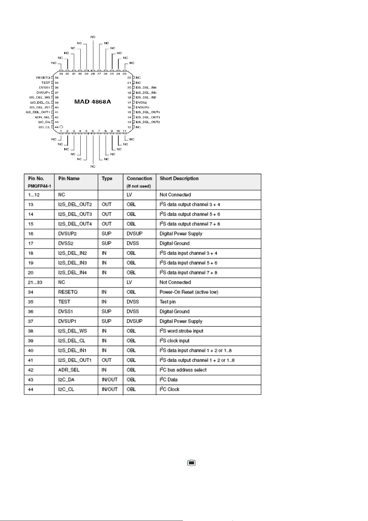
15.31.4.
Pinning
15.32. SVP-EX 59B
General Description
To improve the video quality of the PAL CVBS and HD video input, the all layer changed EX59 improve video sharpness
function in HD channel and enhance the 3D PAL quality compared to EX52 Rev. D chips.
16.SERVICE MENU SETTINGS
To enter the service menu, first enter the MENU by pressing “ ” button and then press the digits 4, 7, 2 and 5
respectively.
TFT TV Service Manual
38
Page 43

Service Menu Items
16.1. Picture Adjust
x Source => All possible sources given with the chasis as a list.
x Mode => Three items as a list; NATURAL, DYNAMIC, CINEMA
x Colour Temp => Three items as a list; COOL, NORMAL, WARM
x Contrast => Slider Bar. Changing value between 0 to 63.
x Brightness => Slider Bar. Changing value between 0 to 63.
x Sharpness => Slider Bar. Changing value between 0 to 16.
x Colour => Slider Bar. Changing value between 0 to 99.
x R => Slider Bar. Changing value between 0 to 100.
x G => Slider Bar. Changing value between 0 to 100.
x B => Slider Bar. Changing value between 0 to 100.
In this menu preset values for each Mode (Contrast, Brightness, Sharpness, Colour values for each ModeNATURAL, DYNAMIC, CINEMA) and for each Colour Temp. (R, G, B values for each Colour Temp- COOL,
NORMAL, WARM) are determined for each source.
16.2. SOUND1
x Menu Subwoofer => If ON, Subwoofer option is available in TV set, and the item is visible
in sound menu, else Subwoofer is not available.
x Subwoofer Level (dB) => This value is gain value of Subwoofer output in dB. - 30...12
x Subwoofer Corner Freq. (x10Hz) => Last low frequency value that is amplified. 5...40
x Menu Dolby Prologic => No functionality now.
x Menu Equalizer => If ON, visible in sound menu, else invisible.
x Menu Lineout => No functionality now.
x Menu Headphone => If ON, visible in sound menu, else invisible.
x Menu Hyper Sound => If ON, visible in sound menu, else invisible.
x Menu Wide Sound => If ON, visible in sound menu, else invisible.
x Menu Dynamic Bass => If ON, visible in sound menu, else invisible.
x Menu Virtual Dolby => If ON, visible in sound menu, else invisible.
x Carrier Mute => If ON, in the absence of an FM carrier the output is muted, else not.
x Virtual Dolby Text => Active if VIRTUAL DOLBY is ON. According to the selection; seen in
sound menu as 3D PANORAMA or VIRTUAL DOLBY.
16.3. SOUND 2
x AVL => AVL is controlled from this menu by service user. ON/OFF
x Menu AVL => If ON, AVL item is visible in sound menu, and AVL can be controlled from
sound menu by normal user, else AVL is invisible to normal user.
x FM PRESCALE AVL ON => If AVL ON, set value in this item is used as prescale value
for the related standard. 0...127
x NICAM PRESCALE AVL ON => If AVL ON, set value in this item is used as prescale value
for the related standard. 0...127
x SCART PRESCALE AVL ON => If AVL ON, set value in this item is used as prescale value
for scart outputs. 0...127
x SCART VOLUME AVL ON => If AVL ON, set value in this item is used as volume value for
scart1 and scart2. 0...127
x FM PRESCALE AVL OFF => If AVL OFF, set value in this item is used as prescale value
for the related standard. 0...127
x NICAM PRESCALE AVL OFF => If AVL OFF, set value in this item is used as prescale value
for the related standard. 0...127
x SCART PRESCALE AVL OFF => If AVL OFF, set value in this item is used as prescale value
for scart outputs. 0...127
x SCART VOLOUME AVL OFF => If AVL OFF, set value in this item is used as volume value for
scart1 and scart2. 0...127
16.4. Options
x Screen Saver =>
x FIRST APS => If ON, first APS menu is opened when the TV opened with the
factory default settings.
TFT TV Service Manual
39
Page 44

x APS VOLUME => After First APS function finishes, the volume of the TV is that value.
x AGC => Tuner AGC value.
x Factory Reset => OK to activate. When OK pressed on this item, factory defaults
loaded.
x Enter Flash Mode =>
TV Norm
x BG => If ON, supported, else not supported
x DK => If ON, supported, else not supported.
x I => If ON, supported, else not supported.
x L => If ON, supported, else not supported.
x LP => If ON, supported, else not supported.
x M => If ON, supported, else not supported.
Features
x PIP/PAP => If ON, PIP/PAP available else not.
x Blue Background => If ON, Blue Background is visible in Features Menu else not.
x Menu Transparency => If ON, Menu Transparency is visible in Features Menu else not.
x Menu Timeout => If ON, Menu Timeout is visible in Features Menu else not.
x Backlight => If ON, Backlight is visible in Features Menu else not.
x Single Tuner =>
Teletext
x Teletext Language => Teletext Language may be controlled from this menu by service
user.
x Menu Teletext Language => If ON, Teletext Language item is visible in Features Menu, and
Teletext Language can be controlled from Features Menu by normal user, else Teletext Language is
invisible to normal user.
Source
x TV
x SC1
x SC2
x SC2 SVHS
x SC3
x SC3 SVHS
x YPBPR
x FAV
x SVHS
x HDMI
x PC
This menu is related with the options of the chassis. These items may be ON or OFF. If ON, the source is
available in TV set, and the item is visible in source menu, else the source may be available but invisible to user.
TFT TV Service Manual
40
Page 45
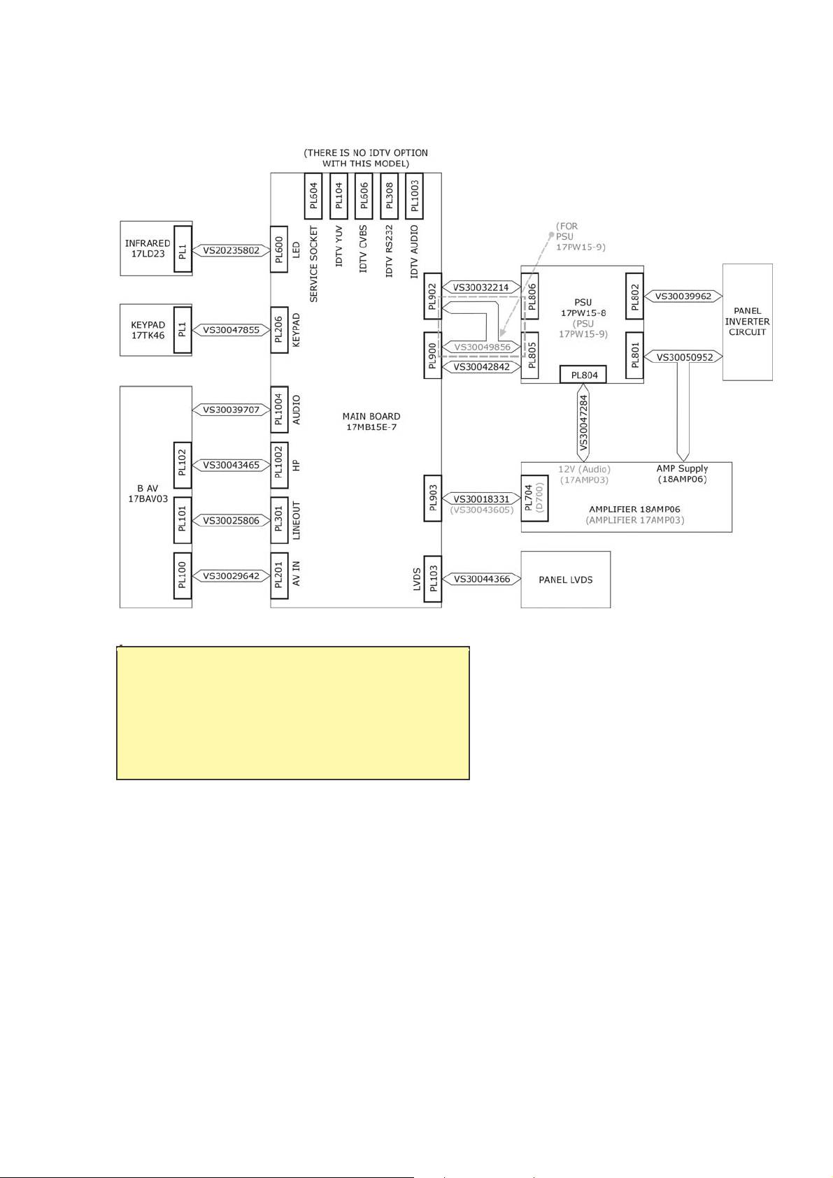
17. CABLE CONNECTIONS
Note
To Change Power Board from 17PW15-8 to 17PW15-9:
• Remove Cables VS30032214 and VS30042842
• Replace with Cable VS30049856
TFT TV Service Manual
41
Page 46
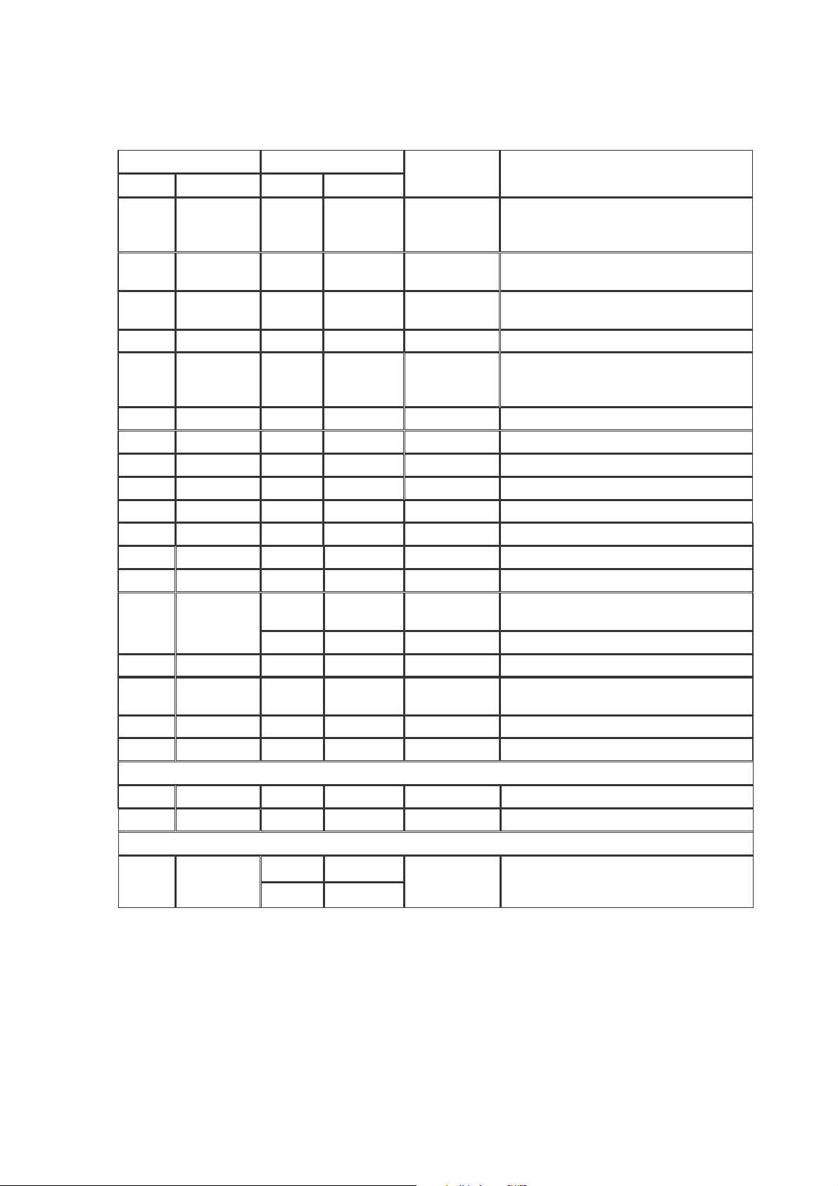
17.1. Cable Descriptions
From To
CRN Board CRN Board
PL801 17PW15-8
PL802 17PW15-8 -
PL804 17PW15-8
PL807 17PW15-8 - - - No IDTV Option
PL103 17MB15E-7 -
PL104 17MB15E-7 - - - No IDTV Option
PL201 17MB15E-7 PL100 17BAV03 VS30029642 CONNECTOR 8P/600
PL206 17MB15E-7 PL1 17TK46 VS30047855 CNAS 2P/600 DIS W/DCAWG24 RoHS
PL301 17MB15E-7 PL102 17BAV03 VS30025806 CONNECTOR 4P/450 SIS W/DC
PL308 17MB15E-7 - - - No IDTV Option
PL600 17MB15E-7 PL1 17LD23 VS20235802 PWB LED BOARD
PL604 17MB15E-7 - - - No IDTV Option
PL606 17MB15E-7 - - - No IDTV Option
PL903 17MB15E-7
PL904 17MB15E-7 - - - No IDTV Option
PL1002 17MB15E-7 PL101 17BAV03 VS30043465
PL1003 17MB15E-7 - - - No IDTV Option
PL1004 17MB15E-7 - 17BAV03 VS30039707 CABLE 5P/320 SHL W/DC
(Amp
Supply)
(12V
Audio)
D700 17AMP03 VS30043605
PL704 18AMP06 VS30018331 CONNECTOR 2P-4/7
Panel
Inverter
+ 18AMP06
Panel
Inverter
17AMP03 VS30047284 CABLE 4P/425SIS W/DC-> AMP03
Panel
LVDS
Input
Part
No.
VS30050952 CABLE 10P-12-4/400 SIS-> AMP06
VS30039962
VS30044366 CABLE 30P/130 QDIA UL20276*
CNAS12P-14/500 W/BLK
UL1007AWG24 ROHS
CNAS 4P-1/600 W/C UL1007 AWG24
RoHS
CNAS 4P-3/600 W/RED DC UL1007
AWG24 RoHS
Description
WITH 17PW15-8 Power Board:
PL805 17PW15-8 PL900 17MB15E-7 VS30042842 CONNECTOR 7P/300
PL806 17PW15-8 PL902 17MB15E-7 VS30032214 CONNECTOR 12P/200 SIS W/DC
WITH 17PW15-9 Power Board:
PL805 17PW15-9
TFT TV Service Manual
PL900 17MB15E-7
PL902 17MB15E-7
42
VS30049856
CNAS12+12+7P/300-200W/DC
UL1007AWG24RoHS
Page 47
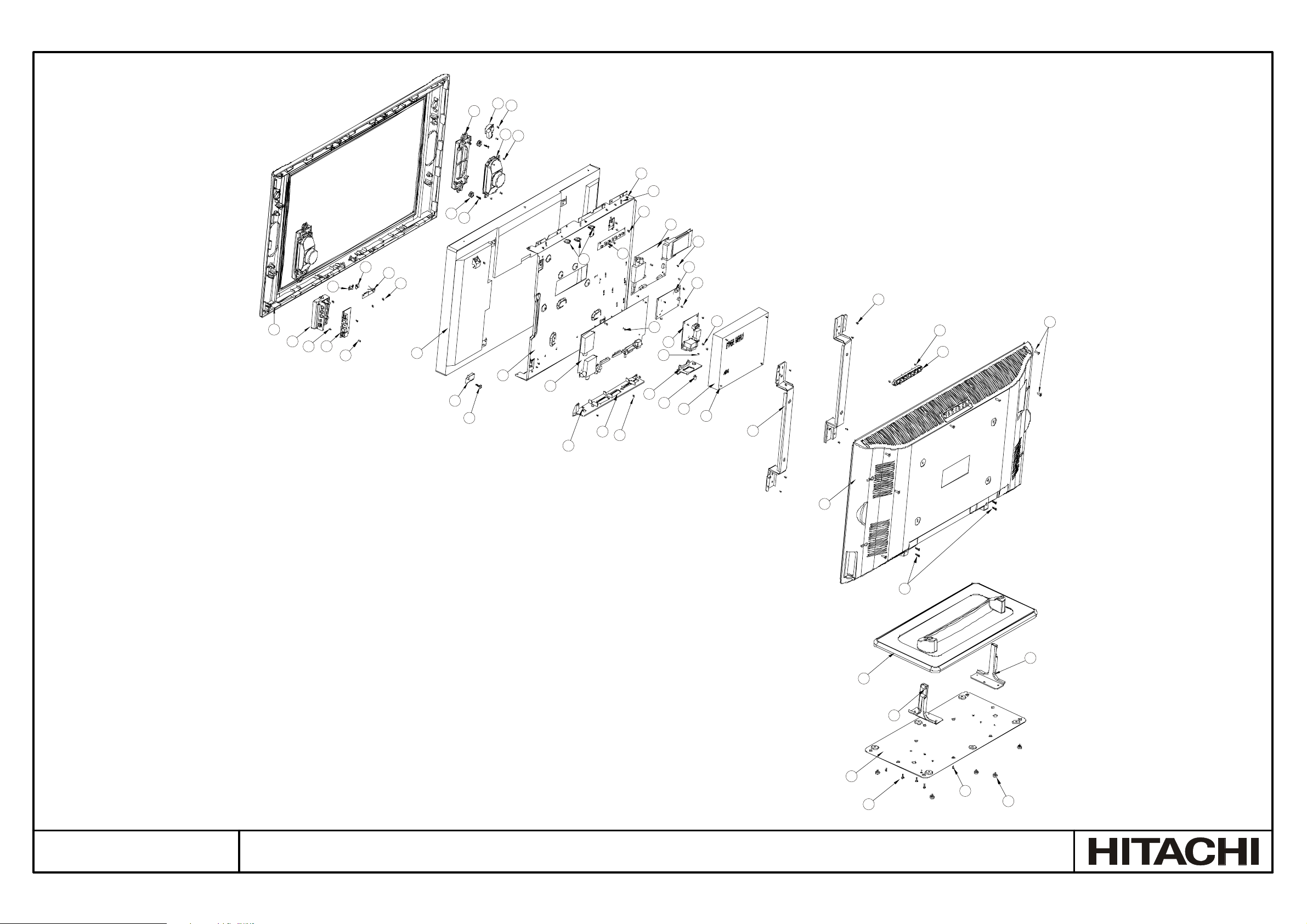
18. APPENDIX A
18.1. ASSEMBLY DRAWING
10
12
11
13
14
21
44
15
16
2
8
3
1
4
5
7
6
9
17
20
31
18
19
22
33
34
28
23
24
27
25
26
43
32
36
39
38
55
40
35
37
30
29
41
42
45
46
No. 0232
TFT TV Service Manual
ASSEMBLY DRAWING
43
54
47
49
48
50
52
51
53
Page 48
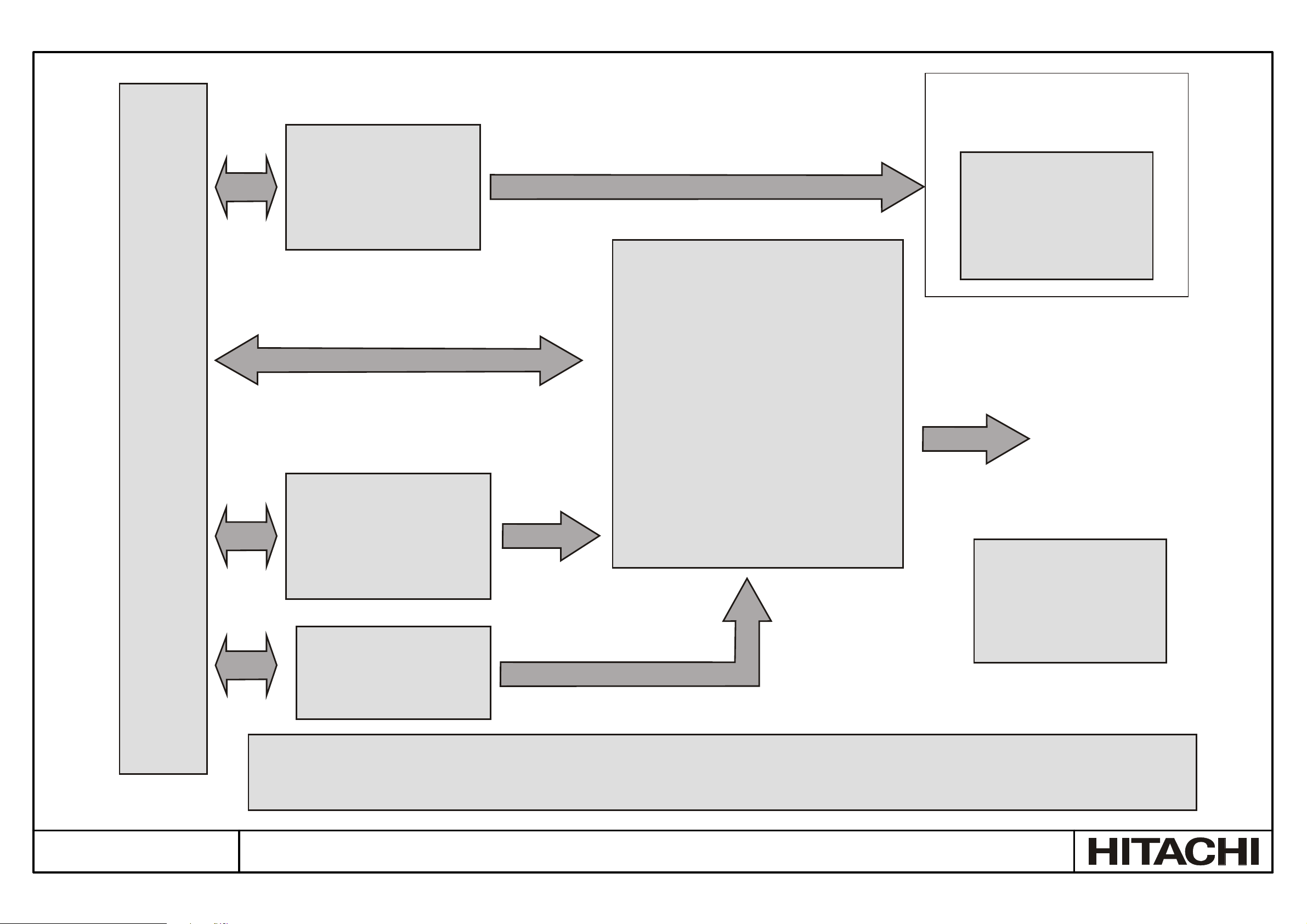
19. APPENDIX B
19.1. BLOCK DIAGRAM
MAIN BOARD
AUDIO AMP BOARD
AUDIO
DECODING
MSP3411G
MICRONAS
IDTV, SVHS, MMC (RGB), PC IN
MAIN_L, MAIN_R
AUDIO
AMPLIFIER
D-CLASS
SVP-EX59
LVDS OUT
VPC3230D
8-BIT YUV
VIDEO PROCESSOR
PIP PICTURE
MICRONAS
AUDIO / VIDEO / GRAPHICS IN / OUT
24-BIT RGB
HDMI DECODER
SIL9993
SDA5550
MCU
MICRONAS
PSU
No. 0232
TFT TV Service Manual
GENERAL BLOCK DIAGRAM
44
Page 49
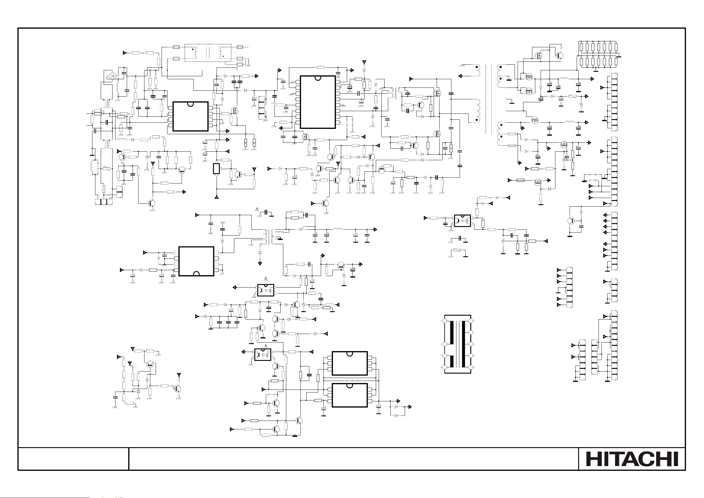
19.2. SCHEMATIC DIAGRAMS
VCC1
R941
PL809
R940
R819
330k
C890
1u
450V
L802
1M
R805
210u
C802
1M
R806
1u
450V
C883
1u
BA159_SMD
R921
1k
Q822
BC858B
50V
C801
33u
50V
VCC2
1M
1M
R927
1M
R926
10k
R924
6k8
1M
R807
C805
D832
R918
10k
50V
470n
C887
470n
BZT55C5V6
VCC2
1k
R929
TL431SAMF2
R951
1k8
50V
Opto
R930
10n
220k
D862
10k
D838
16V
R913
TL431SAMF2
R982
1M
1M
27k
R803
L813
1m9
C886
100k
2
1
R928
R925
C873
R981
R980
L814
+400V
D800
GBU4M
1
2
4
3
TR802
1M
2X12m
1M
R912
150n
1M
R932
C800
250V
2n2
4kV
1
2
4
3
TR801
2X12m
R801
S802
22u
VAR-510V
F800
3.15A
3
2
1
PL800
VF_MAIN
+400V
16V
C882
100n
1M
R917
D850
Q824
1N4148
R818
330k
R950
8k2
R813
C869
1u
16V
VCC1
C808
R880
1k5
6k8
10k
R919
R931
R914
1M
16V
47k
C892
10u
50V
BC858B
D835
R923
R817
100k
1u
C868
Q820
BC848B
D836
330k
16V
C870
2k7
R815
1M
R915
100n
R959
R944
47k
8V2_ZENER
R922
10k
R920
47k
C856
1n
50V
SMPS-RESONANT_PFC
4
IC802
560k
R942
SW_OFF2
EN/UV
TNY266
IC806
+12SV
8
50V
50V
1N4148
10u
10u
D853
TR806
C912
2n2
50V
5
C903
8D1A
7D1
6D2A
5D2
C881
C814
LM317T
VF_MAIN
D
NC
S3
S4
R962
6k8
R963
R820
3k3
IC828
120k
R953
VOUT
10n
VIN
5
6
7
8
C908
1u
16V
SEC
10 11 12
D831
BA159_SMD
C889
470n
50V
10k
R983
D863
1N4148
R823
15R
10k
R977
PFC_OFF
VCC2
10R
VCC1
R968
1k
2
1
ADJ
3
9k1
R969
1kV
C810
10n
630V
D806
BA159_SMD
Opto
D842
1N4148
16V
10u
C906
1u
16V
ON/OFF
+3.3VSTBY
+5V
Q803
MTP6N60E/
SSP7N60A
Q835
BC848B
R814
C874
C907
1u
16V
ST_BY
R897
47k
C888
470n
50V
D824
STPS745
R829
120k
10k
R946
9
7
C819
220u
450V
R893
10k
120R
+3.3VSTBY
R987
10k
0R47
R1003
R826
PL808
56k
R947
R830
R822
BC848B
Q831
1k8
4
3
R828
47k
R986
3k3
0R47
ON/OFF
47k
BA159_SMD
4
3
1N4148
12k
R933
IC811
TCET110G
SW_OFF
4
3
2
1
VFB
C813
2n2
4kV
TR803
G00143A
5
4
3
2
1
D807
VF_MAIN
IC801
TCET110G
D865
BC848B
Q805
BC848B
R988
3k3
C913
Q833
R832
BC848B
Q843
S800
Q828
MTP3N60E
TRF_SAFE_TFT_RES
8
7
6
5
4
3
2
1
1k
R871
1
2
26V
10
16V
9
GND
8
3V3
7
5V
6
R967
1k
1N4148
D855
R872
TR805
10k
47R
R873
TL431SAMF2
FUSE_SMD_7A/
32VDC_1206
+24V
D856
1N4148
+12V
D819
9
10
11
12
13
14
15
16
F801
F802
R874
1k
C849
50V
2n2
24VDC
Q816
MTP6N60E/
SSP7N60A
+24V
F803
FUSE_SMD_7A/
32VDC_1206
+5WOREG
4k42
D845
UF5402
D846
UF5402
+5SV
100V
R875
Q815
MTP6N60E/
SSP7N60A
+12SV
27n
33k
D818
BA159_SMD
160V
1u
Q827
MTP6N60E/SSP7N60A
470u
C806
R985
2k2
Q842
STP20NE06LFP
56k
R984
C855
R876
30k
R877
VCC_3V3_ON
+400V
C905
R836
12k
C910
1kV
C822
Freq
IC827
1N4148
R966
R834
10k
10k
R949
R843
R948
1u
3k3
100R
BC848B
12V
D854
12k
1k8
R824
3k3
R838
3k3
16V
50V
R825
1n
Q802
50V
C909
10u
100R
R889
100R
R888
D823
BA159
100k
1
2
3
4
5
6
7
8
1u
C826
SW_OFF2
3
1
IC825
STPS5L25B
25V
100R
R890
R881
R964
1k8
R839
1kV
10n
10n
C902
R837
150R
D805
1N4148
6
7
8
9
10
1
2
R892
10k
16V
1u
Q834
BC848B
1
2
10k
R833
Q804
BC848B
33k
R847
10k
IC807
INV.IN
N.I.IN
SYNC
OSC.OUT
CT
CT
DISCH 10
CS
Q837
BSH103
16V
R973
BC848B
R974
Q818
1k
D809
1kV
220p
C859
4
2
1kV
220p
C815
1k8
10k
R887
R882
10k
D851
TL431SAMF2
10k
R965
BZT55C3V9
R831
3k3
C824
BC848B
Q806
15k
15V
D847
16V
SG2525A
C898
470R
R849
C817
220u
25V
3k3
R883
+12V_2
100n
R844
R846
100R
+24V
R970
47k
BC848B
C818
4700u
6V3
100R
50V
2n2
Q807
R850
100k
3u3
VREF
OUT_B
GND
SHUTD
COMP.
50V
R910
47k
Q838
+12V_2
1k
C862
100n
63V
R879
1k
27R
R884
+5V
C901
+VI
BC848B
C857
4700u
6V3
R851
1
2
3
1
2
3
R855
D1
D2
G
D1
D2
G
C833
16
15
14
13VC
12
11OUT_A
100k
9
L804
22u
SW_OFF
BC848B
50V
100n
50V
R857
12k
Q810
BC848B
Q808
2200u
BC548C
Q809
D810
+3.3VSTBY
NTGS3446
NTGS3446
IC824
33u
C860
IC826
S801
5VREF
100n
63V
S803
R852
10k
R856
4k7
BZT55C3V9
6V3
BZT55C5V6
C834
D826
R961
10R
C836
S804
C838
10u
50V
50V
R858
R859
33u
4k7
33k
R952
1N4148
C839
+5VSTBY
D4
D3
D4
D3
D811
S
S
VCC1
22R
C835
5VREF
4k7
D858
BA159_SMD
22R
R976
5n6
D859
R891
16V
100n
C830
100n
16V
6
5
4
6
5
4
50V
BAT254
BC858B
Q811
47k
16V
15R
R975
BAT254
BC848B
R862
+3.3VSTBY
100u
D860
C895
5VREF
C837
Q812
R863
33k
1
2
3
4
G00137D
C897
2n2
50V
50V
33u
TR804
D840
BA159
D841
BA159
R866
10k
R978
C840
+400V
6
8
5
7
R979
R861
10R
1k5
C900
50V2n2
R972
1k
8k2
R867
VCC_3V3_ON
C896
2n2
R860
50V
10R
BC558B
Q839
1k5
C899
2n2
50V
MTP6N60E/SSP7N60A
R868
6k2
C841
+2.5V
D812
1N4148
BC558B
Q840
D813
1N4148
D857
Freq
D814
1N4148
100n
VFB
MTP6N60E/
SSP7N60A
Q813
630V
12n
C877
10k
R864
R870
5k1
AC_GND
C845
100n
25V
1N4148
50V
100n
A
NC
B
C
C894
27R
R869
50V1nC846
1
3
2
4
5
C878
Q814
10k
R865
25V
D815
R971
4
3
R960
4M7
TR807
630V
12n
0R47
C842
C893
TCET110G
C847
2n2
4kV
IC809
1n
1n
400VDC
1kV
1kV
35V
1000u
BA159_SMD
D820
C848
16V
1000u
+5WOREG
16V
2k2
R958
+5V
BZT55C3V9
D864
+24V
+2.5V
+33V
+12V
+5V
Q829
BU2508AF
L810
2u7_RESONANT
C850
C911
160V1uC853
C851
Q832
STP20NE06LFP
D852
TL431SAMF2
BC858B
Q841
+5VSTBY
+3.3VSTBY
25V
L811
2n2
PL807
4700u
R878
10k
50V
C884
A/D_DIM_SEL
1
2
3
4
5
6
7
1k
1k
35V
16V
1000u
1000u
C812
R956
R957
10k
1M
C852
D821
C863
1000u
D_DIM
A_DIM
D861
C904
VCC_3V3_ON
1
2
3
4
5
6
7
PL806
10k
R998
10k
R997
R996
1M
R9901MR9911MR9921MR993
R989
+24V
+24V
+33V
BZT55C33
+12V
+5V
16V
+24V
S806
S805
BL_ON/OFF
BL_ON/OFF
BAT254
A_DIM
D_DIM
16V
1u
A/D_DIM_SEL
ST_BY
+33V
+12V
+12V
1
2
3
4
5
6
PL810
10k
R1002
10k
R1001
10k
R1000
10k
R999
1M
R9941MR995
PL801
1
2
3
4
5
6
7
8
9
10
PL802
1
2
3
4
5
6
7
8
9
10
11
12
PL803
1
2
3
4
5
6
7
8
9
10
PL804
1
2
3
4
PL805
1
+5V
2
3
4
5
6
7
8
9
10
11
12
PRI
6
1
1u
100k
N1 N2
32
16V
S1
1
G1
2
IRF7314
S2
3
G2
4
100k
R945
BC848B
Q830
+400V
4
3
S2
2
S1
1
BP
100n
C829
16V
+5SV
PFC_OFF
Q823
BC548C
No. 0232
TFT TV Service Manual
POWER BOARD (RESONANT MODE TFT PSU)
45
Page 50
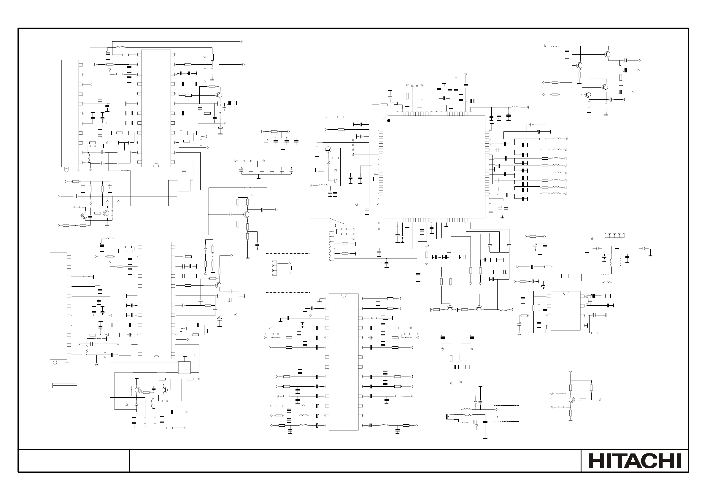
VCC5V_FILTERED
IF1
SAW_SW2
TU1001
CTF5543_HOR
SW01=H L’
SW01=L BG, DK, I, L
TU1000
CTF5543_HOR
R1121
10k
AGC
1
TU
2
AS
3
SCL
4
5SDA
NC
6
VS
7
8NC/ADC
9VST
10IF2
11IF1
R1124
100R
C1193
50V
10n
S2013
BC848B
Q1015
50V
47u
C2200
VCC5V_FILTERED
50V
15k
R1048
C1052
10p
25V
4k7
R1049
TUN1_CVBS
C1196
100n
50V
47u
C2201
VCC5V_FILTERED
QSS_TUN2
10u
S1003
TUN2_CVBS
VCC_33V
R1127
4R7
100n
C1197
C1198
VCC5V_FILTERED
2k4
R1050
Q1005
BC848B
75R
R1051
560R
R1052
C1054
SC2_AUDIO_L_IN
IDTV_L_IN
SC3_AUDIO_L_IN
PC_AUDIO_L_IN
YPBPR_AUDIO_L_IN
50V
50V
50V
100n
C1055
22n
50V
22n
50V
AUDIO_L
AUDIO_R
AUDIO_L2
R1128
4R7
10u
C1201
C1202
VCC5V_FILTERED
50V
100n
C1200
C1199
PL1003
1
2
3
IDTV AUDIO IN
S2002
S2001
DAC_AOL
DMP_L_IN
R2015
100R
R2016
100R
50V
100n
50V
100n
QSS_TUN1
100R
R2203
50V
R2013
R2014
R2205
100n
50V
C1205
C2010
100n
16V
R2010
R2011
R2012
1k
1k
1k
C2021
C2023
33V_FILTERED
50V
100n
C1203
100n
IDTV_L_IN
IDTV_R_IN
1k
50V
1k
1k
1n
1n
1n
C247
C1204
C1206
VCC_5V
8V_FILTERED
1n
50V
1n
C2013
1n
50V
1n
1n
C2019
1n
C2105
L2001
BLM21B201S
L2002
BLM21B201S
L2018
50V
HARDWARE MUTE
C2009
C2011
C2015
C2017
50V
SCL
SDA
1k
R1068
470R
R1067
L1008
22u
50V
C2012
330n
C2014
330n
C2016
330n
16V
C2018
330n
C2020
330n
C2108
330n
16V
C2022
22u
C2024
22u
50V
22u
C254
R1070
100R
R1071
100R
Q1007
BC858B
R1069
470R
IC206
BZT55C3V6
IC207
1N4148
C1080
100u
C1079
C1078
1n5
10u
50V
50V
RESETQ_MSP
6
5
4
3
2
1
PL1004
IC2000
GND
1
CAPACITANCE
2
VS
3
L1
4
L2
5L
L3
6
NC
7
TEA6422D
8 NC1
9L4
10 L5
11 L6
12 LOUT1
13 ROUT1
14 LOUT2 15ROUT2
8V_FILTERED
QSS_TUN2
QSS_TUN1
R1091
50V
R1093
X1002
53
TESTEN
100R
100R
C1001
AUDIO_R_LINE_OUT
3
2
1
C1122
R1094
1n
50V
C1123
56p
C1125
52
ANA_IN2+
R1097
C1128
56p
C1130
56p
56p
50
51
ANA_IN-
ANA_IN1+
50V
1n
C1126
AUDIO_R_OUT
R1096
1k
C1132
100R
C1000
1n
50V
AUDIO_L_LINE_OUT
L216
L219
L218
49
AVSUP
MONO_IN
SC1_IN_R
SC1_IN_L
SC2_IN_R
SC2_IN_L
SC3_IN_R
SC3_IN_L
SC4_IN_R
SC4_IN_L
100R
R1095
SC2_AUDIO_L_OUT
D1005
BZT55C5V1
AVSS
VREFTOP
ASG1
ASG2
ASG3
AGNDC
AHVSS
R1098
BC848B
Q1011
22u
50V
100R
AUDIO_L_OUT
C255
D1004
BZT55C5V1
1n5
10u
C1144
560p
C1137
48
N.C
47
C1156
46
45
C1138
330n
44
330n
43
C1157
42
330n
C1148
41
330n
40
C1158
39
330n
C1140
38
330n
37
C1164
36
C1147
330n
35
34
33
10u
50V
330n
C1145
C1149
100n
3u3
50V
C1134
50V
50V1nC1133
1n5
C1150
16V
100u
50V
C1151
470p
C1136
VCC5V_FILTERED
L1017
4n7
PC_AUDIO_R_IN
PC_AUDIO_L_IN
4n7
50V
C257
DMP_IR_SW
DMP_IR_SW2
VCCA_3V3
VCCA_3V3
1p8
50V
1p8
C1116
R2202
SUBW
N.C
58
NC4
IC208
1n
C2202
220R
AUD_CL_OUT
C1118
50V
R1092
1k
18.432MHz
56TP57
1n
C1119
55
XTAL_OUT
100R
100R
C1124
C1120
R1089
1n
50V
R1090
50V
SC2_AUDIO_R_OUT
JK200
JACK-AK16
54
XTAL_IN
100R
C1121
BC848B
Q1009
22u
C1113
4k7
R107
62
ADR_SEL
C1117
50V
4k7
R104
61
59
60
NC5
C_CTR_I/O_0
D_CTR_I/O_1
MSP3452G
1n
50V
100u
1n
SC2_AUDIO_R_IN
IDTV_R_IN
SC3_AUDIO_R_IN
PC_AUDIO_R_IN
YPBPR_AUDIO_R_IN
DAC_AOR
DMP_R_IN
AUDIO_R2
100n
25V
R1078
100R
63
50V
39p
C1084
470p
50V
C1086
MAIN_R
MAIN_L
C2028
C2034
C2037
C2107
330n
C2030
C2031
330n
330n
330n
C251
1
2
3
4
5
6
7
8
9
10
11
12
13
14
15
ESD
16
C1087
470p
1kV
HP_R
HP_L
47p
C2025
C2026
47p
S2000
1n
50V
1n
50V
330n
1n
50V
330n
16V
50V
22u
BLM21B201S
39p
C1085
I2S_CL
I2S_WS
I2S_DA_OUT
I2S_DA_IN1
270p
50V
C1081
S106
VCCA_3V3
S105
VCC_5V
MUTE_AMP
R105
3k3
R106
3k3
SDA
28
SCL
27
ADDR
26
R1
25
R2
24
R3
23
NC3
22
21NC2
20R4
19R5
18R6
17ROUT3
16LOUT3
64
NC6
12C_CL
12C_DA
12S_CL
12S_WS
12S_DA_OUT
12S_DA_IN1
ADR_DA
ADR_WS
ADR_CL
DVSUP
DVSS
12S_DA_IN2
NC1
NC2
NC3
RESETQ
C1097
1n
1n
C2106
L2019
STANDBYQ
DACA_R18DACA_L19VREF220DACM_R21DACM_L22DACM_C23DACM_SUB24DACM_S25SC2_OUT_R26SC2_OUT_L27VREF128SC1_OUT_R29SC1_OUT_L30CAPL_A31AHVSUP32CAPL_M
17
C1112
50V
1n
1n
50V
C1114
50V
1n
C1106
R2017
SDA
100R
R2018
SCL
100R
R2019
C2027
1k
R2020
C2032
C2033
C2036
S2009
1k
S2003
R2021
1k
R2022
1k
R2023
1k
R2206
1k
1n
50V
R2204
100R
1n
50V
C249
C2029
C1152
C1154
50V10u
HP_R
L1018
C1177
C1176
C1170
C1171
C1153
VCC_8V
C1162
100n
8V_FILTERED
1u
50V
C1174
C1175
C1163
R1129
HP_L
1n
1n
1n
1n
1n
1n
1n
4R7
R1100
1n
4k7
C1159
AUDIO_L_OUT
AUDIO_R_OUT
VCC_5V
100n
C1166
4R7
R1130
10u
50V
1u
C1165
C1167
R1101
100u
10k
10u
C1169
R1102
C1168
R1104
1k
R1108
R1110
R1111
R1109
C300
47k
MUTE_AMP
MUTE_AMP
C1173
2n2
R1105
R1106
R1107
C295
1k
1k
1k
1k
1k
1k
1k
R1103
L2000
R2004
100R
R2005
100R
8V_FILTERED
16V
100n
4k7
C1172
100u
8 VDD
7OUTB
50V
220p
6 INB-
L1020
L1023
L1024
L1025
L1026
L1019
L1022
L1021
C1178
IC209
TDA1308
S107
Q100
BC848B
S108
C2004
470p
50V
Q2001
BC848B
1k
R2006
BC848B
1k
R2007
SC1_AUDIO_R_IN
SC1_AUDIO_L_IN
AV_AUDIO_R_IN
AV_AUDIO_L_IN
AUDIO_R
AUDIO_L
AUDIO_R2
AUDIO_L2
HEADPHONE
1n
C1180
100u
1OUTA
47k
R1112
2INA-
C1181
3INA+
4VSS5 INB+
STBY_3V3
4k7
R100
4k7
R103
R101
R102
4k7
S2010 & R2208 are for mute option
Mute is active high
Q2002
BC848B
50V 22u
C2005
50V 22u
C2006
1k
R2009
Q2003
BC848B
50V 22u
C2008
1k
R2008
4
L1029
60R/
100MHZ
500mA
L1028
L1027
60R/100MHZ_500mA
C1183
1n
C1184
2n2
HEADPHONE
50V 22u
PL1002
Q2004
D1000 D1001
C1182
2n2
50V
C1179
220p
10u
10k
R1113
4k7
C2007
L1030
SC3_AUDIO_R_OUT
123
SC1_AUDIO_R_OUT
C1185
2n2
50V
SC1_AUDIO_L_OUT
SC3_AUDIO_L_OUT
L1003
26R_100MHZ_1.5A
25V
BA782
47u
25V
C1011
C1012
R1004
C1194
L1001
50V
R1005
100R
SDA
VCC_5V
100R
SDA
C1056
R1013
100R
12 SIOMAD 13NC
11 SCL
33p
25V
C1020
R1008
100R
33p
25V
R1011
5k6
2
IN2
IN11
SF_63962
16V
100n
D1007
D1003
S1010
R1009
100R
VCC_5V
R1012
5k6
2
IN2
IN11
1n
50V
Z1000
BA591
K3953M
GND
S1009
Z1001
GND
C1024
C1025
3
OUT2
OUT1 4
R1010
100R
R1114
C1026
C1027
3
OUT2
OUT1 4
BA591
C1021
390p
C1022
C1023
390p
10 SDA
33p
25V
9 TOP
8AUD
7 DGND
C1028
470n
63V
C1029
10n
50V
10n
50V
50V
TDA9885T
6 AFD
5 DEEM
4 FMPLL
3 OP1
2 VIF2
5
1 VIF1
IC200
SIOMAD
12
2k2
SCL
11
33p
25V
SDA
10
33p
25V
TOP
9
AUD
8
DGND
7
C1030
AFD
6
470n
63V
C1031
DEEM
5
10n
50V
4 FMPLL
10n
50V
3 OP1
50V
2 VIF2
5
1 VIF1
TAGC
REF
VAGC
CVBS
AGND
TDA9885T
VPLL
IC201
R1120
10k
BC848B
Q1014
16V
100n
C1189
L1031
R1116
BC848B
Q1013
S2012
10k
1u
C1186
R1115
100R
47k
S1005
R1118
D1006
D1002
BA782
1k
16V
R1117
100n
C1188
R1029
14TAGC
100R
C1034
X1000
15REF
22p
4MHz
25V
C1036
16VAGC
470n
63V
R1025
17CVBS
47R
18AGND
C1037
19VPLL
100n
25V
20VP
22k
R1022
C1035
21AFC
100n
25V
22k
22OP2
R1028
23SIF1
24SIF2
3
GND
2
5
IN2
OUT2
IN11
OUT1 4
K9356M
Z1003
NC
13
R1030
14
100R
C1038
X1001
15
22p
4MHz
25V
C1039
16
470n
63V
47R
17
R1026
18
C1040
19
220n
16V
VP
20
22k
R1023
21AFC
VCC_5V
2
R1024
IN2
IN11
6k8
GND
K9356M
Z1002
R1027
SAW_SW1
3
5
OUT2
OUT1 4
10k
R1119
IF
VCC5V_FILTERED
22OP2
23SIF1
24SIF2
C1187
10n
50V
16V
12k
IC204
R1036
1N4148
10k
47k
75R
R1032
R1037
R1043
VCC_5V
R1042
220R
Q1003
BC848B
1n5
50V
6k8
R1031
VCC_5V
1n5
50V
C1041
100n
25V
22k
SAW_SW1
C1042
R1038
330R
50V
VCC5V_FILTERED
SAW_SW2
12k
IC205
1N4148
47k
10k
R1034
R1035
2k2
Q1002
BC848B
C1043
R1041
150R
50V
47R
R2200
16V
100n
C1195
10n
C1045
10u
16V
C1048
VCC_5V
R1039
R1040
75R
R1044
47R
R2201
10n
C1047
10u
16V
C1049
47u
50V
C1014
1AGC
SCL
2TU
3AS
VCC_5V
4SCL
5SDA
6NC
7VS
8NC/ADC
9VST
10IF2
11IF1
1u
16V
R1122
10k
S1000
1u
C1192
33p
C1007
C1013
10u
50V
25V
100n
C1002
10u
50V
C1006
33V_FILTERED
R1000
2k2
S1008
C1005
1n
50V
1u
L1002
C1057
1n
50V
IF1
1k
10k
R1126
R1125
L1032
R1123
47k
Q1016
BC848B
C1191
16V
100n
C1010
SCL
33p
C1008
33p
25V
C1015
10u
100n
C1003
10u
50V
C1009
33V_FILTERED
R1001
2k2
S1007
C1004
1n
50V
L1000
S1006
IF
No. 0232
TFT TV Service Manual
MAIN BOARD (17MB15E-7) - SHEET 1
46
Page 51
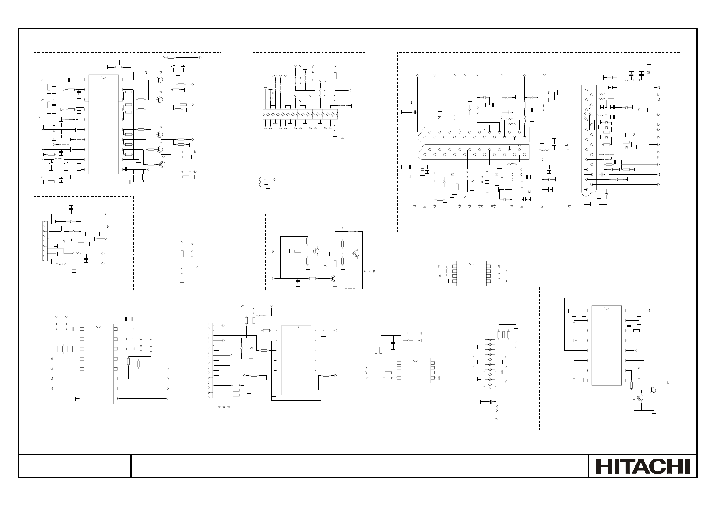
VIDEO SWITCH TEA6415C
SC1_V_IN
SC2_V_IN
TUN1_CVBS
AV1_V_IN
VCC_8V
SVHS_Y_IN
VCC_8V
IDTV/SC3_CVBS
1
2
3
4
5
6
7
8
PL201
R203
R204
16V
C274
220n
16V
R206
39p
75R
50V
C285
SDA
100R
C260
220n
16V
39p
75R
50V
C292
R207
SCL
100R
C265
220n
39p
75R
50V
R200
C259
16V
C279
220n
16V
39p
75R
50V
R205
C280
S200
R201
75R
100u
R202
75R
C288
220n
39p
50V
C297
16V
L200
22u
50V
C299
C283
C291
220n
39p
50V
C268
16V
150p
C261
BZT55C5V1
D215
D217
D216
L202
L201
C272
EXTERNAL INPUT
1 INPUT1
2DATA
47p
25V
C303
3 INPUT2
4 CLOCK
47p
25V
C287
5 INPUT3
6 INPUT4
S201
7 PROG
8 INPUT5
9 VCC
16V
220n
C273
10 INPUT6 11INPUT7
50V
C263
39p
220n
R232
C262
75R
1n
C271
1n
50V
IC210
TEA6415C
AV1_V_IN
SVHS_Y_IN
CIN
AV_AUDIO_R_IN
AV_AUDIO_L_IN
VCC_8V
39p
C304
75R
R264
C282
20INPUT8
220n
16V
19GND2
10k
R220
18OUTPUT6
10k
R221
17OUTPUT5
10k
R222
16OUTPUT4
15OUTPUT3
10k
R223
14OUTPUT2
10k
R224
13OUTPUT1
10k
R225
12GND1
C275
220n
16V
MMC_CVBS
R226
100R
R227
100R
R230
100R
R1033
100R
R2001
100R
TUN2_CVBS
39p
C276
75R
R231
4R7
R229
10u
C298
Q200
BC848B
Q203
BC848B
Q202
BC848B
BC848B
Q2000
V8
BC848B
C294
R235
75R
1k
R239
R240
75R
1k
R241
R237
75R
1k
R242
R1046
75R
R1045
R2002
75R
R2003
VCC_5V
4k7
S651
V8
V8
V8
V8
Q1004
DIMMING SELECTION
16V
100n
MAIN PICTURE
TO SVP
CVBS_SVP
Vx to VPC
GOES TO VPC3230
FOR PIP PICTURE
SC2_V_OUT
SELECTABLE VIDEO OUT
FOR SCART 2
SC1_V_OUT
1k
SC3_V_OUT
1k
VCCA_3V3
S652
R271
V8
VCCA_3V3
5V
VCCA_3V3
LG_1/IRQPDP
VCC_12V
PANEL_VCC
2
DISP_EN/PDWN
1
TXOUT3+
VCCA_3V3
S648
S109
S643
S642
PDP_GO/BL_ON_OFF
3
5
9
7
11
8
6
4
10
12
TXOUT3-
TXCLKOUT-
TXCLKOUT+
13
14
TXOUT2+
4k7
R251
S111
S112
S113
CPU_GO
VCC_12V
21
15
19
17
20
22
18
16
TXOUT2-
TXOUT1-
TXOUT1+
LVDS OUTPUT
PL206
1
IDTV/SC3_CVBS
2
IDTV CVBS INPUT
CHROMA SWITCH
10k
CIN
SEL
CHROMA_SW
C245
220n
R267
R270
100R
16V
C2050
47k
R268
R269
47k
16V
100n
S638
Q204
BC848C
SCL_PANEL
23
24
SDA_PANEL
S639
25
27
28
26
TXOUT0-
TXOUT0+
C246
220n
16V
SVHSfromSC2_C
R250
S641
S646
R274
VCCA_3V3
4k7
29
30
PL103
1k
Q206
BC848C
SC3_V_OUT
IDTV/SC3_CVBS
PANEL_VCC
S640
S647
PARITY
V8
S635
18k
R266
D2000
BZT55C10
D214
BZT55C10
PL205
50V
150p
50V
C252
150p
C2038
SC1_V_IN
150p
C2039
23
24
22
150p
D212
C250
75R
R260
R261
SC1_FB
SC1_V_OUT
SVHSfromSC2_C
S636
D2001
272625
D209
D210
75R
R285
75R
SC1_R
PIN8_SC3
D2002
S221
D219
D206
SCSCL
BZT55C10
R286
SC3_AUDIO_L_IN
BZT55C10
L2005
75R
34333231302928
13121110987654321
SC1_G
D2004
C2044
S220
4n7
SCSDA
BZT55C10
D204
D220
SC1_B
PIN8_SC1
SC3_AUDIO_L_OUT
BZT55C10
330R
R2024
L2003
75R
D202
50V
4n7
C269
D224
BZT55C10
D2105
L2004
D2104
C2042
SC3_AUDIO_R_IN
PL203
BZT55C10
D2003
50V
4n7
C2045
1n
L2006
4n7
50V
C258
L204
L206
1n
50V
C267
R252
330R
D2102
BZT55C10
C286
150p
50V
SC1_AUDIO_R_OUT
D222
BZT55C10
SC1_AUDIO_R_IN
1
3
L211
5
L212
7
9
11
13
15
17
19
21
D221
BZT55C10
C284
4n7
L207
50V
2
L209
R253
330R
C264
4
1n
50V
6
L214
D203
D205
8
75R
R288
D207
10
R289
75R
12
S204
S205
14
R275
16
C248
150p
D218
18
20
D213
50V
BZT55C10
C253
150p
1n
50V
L203
BZT55C10
D2103
150p
C277
C266
4n7
D2100
BZT55C5V1
75R
R290
D208
C2049
C293
100n
150p
16V
75R
R276
D211
50V
C301
330R
R249
BZT55C10
D223
D2101
BZT55C10
150p
C270
SC2_AUDIO_R_OUT
SC2_AUDIO_R_IN
SC2_AUDIO_L_OUT
SC2_AUDIO_L_IN
PIN8_SC2
SC2_B
TV_LINK
SC2_G
SC2_R
SVHS from SC2_C
SC2_FB75R
SC2_V_OUT
SC2_V_IN
SC3_AUDIO_R_OUT
BZT55C10
330R
R2025
C2040
1n
L2008
L2007
3938373635
424140
L213
1817161514
212019
L208
L210
L205
SC1_AUDIO_L_IN
C296
330R
R254
150p
C278
SC1_AUDIO_L_OUT
1n
BZT55C10
D2500
R287
I2C BUFFER FOR PANEL
Q205
BC848C
10k
R273
S633
C_SELECTED
S634
SDA2
SDA_PANEL
S645
IC215
1
NC1
2
NC2
ST24LC21
3
NC3
4
VSS
8VCC
VCC_5V
7VCLK
6SCL
5SDA
SCL2
S644
SCL_PANEL
VCCA_3V3
STBY_3V3
S650
S637
4k7
4k7
4k7
4k7
R265
R277
R246
R248
CHROMA_SW
DISP_EN/PDWN
RGB_SW2
RGB_SW1
PORT EXPANDER
No. 0232
C290
VDD 16
SDA 15
SCL 14
INT 13
P7 12
P6 11
P5 10
100n
16V
STBY_3V3
SDA2
330R
R255
SCL2
330R
R256
4k7
R257
IC213
A01
A12
A23
P04
PCF8574
P15
P26
P37
VSS8P49
D2502
R214
S654
R212
22R
2k
BZT55C12
STBY_5V
S653
R215
22R
R213
22R
IC211
1A1
21Y
32A
42Y
74LVC14A
53A
63Y
7GND 84Y
14VCC
136A
126Y
115A
105Y
94A
STBY_3V3
16V
100n
C289
10k
10k
R217
R216
VGA_VSIN
22R
R238
DDC_DATA_PC
DDC_CLK_PC
VGA_VSIN
100R
R218
100R
R219
1N4148
VCC_5V
D200
1N4148
DDC_5V
D201
16V
100n
C302
IC212
8 VCC
7 VCLK
5 SDA
ST24LC21
1NC1
2NC2
3NC36 SCL
4VSS
D-SUB 15 PC INPUT & DDC CIRCUIT
MMC
VIDEO INPUTS
MMC_CVBS
DMP_L_IN
PL207
75R
75R
75R
R291
R292
R293
12
34
56
78
910
1112
1314
1516
1718
1920
16V
10u
C948
10u
L925
VCC_5V
MMC_R
MMC_G
MMC_B
DMP_IR_SW
DMP_R_IN
DMP_IR
PC STAND-BY
C2051
VGA_VSIN
100n
C2052
150k
R280
10k
R281
VCC_5V
PL200
15
DDC_CLK_PC
14
VCCA_3V3
STBY_3V3
S223
S649
4k7
4k7
R259
R258
LG_1/IRQPDP
RGB_SW3
SW_ENABLE
PANEL_VCC_ON/OFF
13
12
DDC_DATA_PC
11
10
9
8
7
6
5
4
3
2
1
VGA_RIN
VGA_GIN
VGA_HSIN
VGA_BIN
DDC_5V
PGAGND
R208
R209
R210
2k
R211
D2501
BZT55C12
75R
75R
75R
PGAGND
1Q1
100n
2Q2
3Q3
4Q4
5Q5
6Q6
7Q7
8GND
IC214
74HC595D
DSERIAL
Q7OUT
STOP
SHCP
100n
R279
VCCA_3V3
47k
STBY_5V
100n
C2053
10k
VGA_HSIN
10k
R283
Q208
BC848C
Q207
BC848C
PC_STBY
VCC
16
Q0
15
C281
14
OE
13
12
11
MR
10
9
10k
R282
R284
MAIN BOARD (17MB15E-7) - SHEET 2
TFT TV Service Manual
47
Page 52
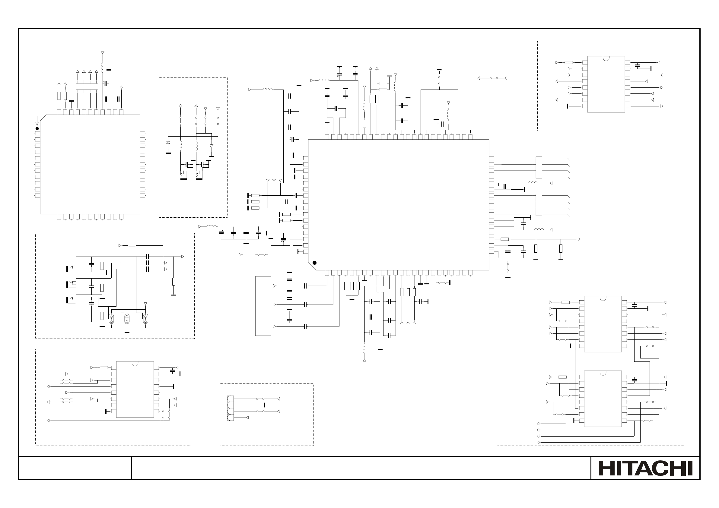
I2S_DA_IN1
SCL
SDA
8
R1R2R3
10R
R2028
123
100R
100R
R2026
R2027
41
42
43
44
SCL
SDA
ADR_SEL
1NC1
2NC2
3NC3
4NC4
5NC5
6NC6
7NC7
8NC8
9NC9
10 NC10
11 NC11
NC1213I2S_DEL_OUT214I2S_DEL_OUT315I2S_DEL_OUT416DVSUP217DVSS218I2S_DEL_IN219I2S_DEL_IN320I2S_DEL_IN421NC1322NC14
12
JK300
WHITE_FAV
JK301
WHITE_FAV
JK302
1P_RED_FAV
I2S_DEL_OUT1
MAD4868A
IC2001
Y
12 3
Pb
12 3
12 3
Pr
YPbPr INPUT
RGB_SW2
RCA_PR
S309
VGA_RIN
RCA_Y
S314
S308
S307
VGA_GIN
RIN2
GIN2
BIN2
VGA & Y PbPr SWITCHING
I2S_DA_OUT
I2S_CL
765
39
40
I2S_DEL_CL
I2S_DEL_IN1
50V
220p
50V
220p
50V
220p
I2S_WS
L2009
C2046
R4
4
C2047
38
DVSUP1
I2S_DEL_WS
C356
75R
C357
75R
C358
75R
R326
1k
VCC_5V
BLM21B201S
10u
50V
10n
50V
36
37
DVSS1
VCC_5V
R331
R332
R333
C2048
1
2
3
4
5
6
7
8
100n
25V
D102
BAV99
35
TEST
A
B
C
D
E
F
G
H
RESETQ_MSP
34
RESETQ
NC25
NC24
NC23
NC22
NC21
NC20
NC19
NC18
NC17
NC16
NC15
4k
R312
D104
BAV99
IC318
PI5V330_SOIC
220n
220n
220n
IC316
C362
R
16
O
15
100n
N
14
M
13
L
12
K
11
J
10
I
9
C351
16R
15O
100n
16V
14N
13M
12L
11K
10J
9I
C352
16R
15O
100n
16V
14N
13M
12L
11K
10J
9I
S312
SC2_FB
S344
S342
S340
VCC_5V
SC1_FB
FB_VPC
SC1_B
SC2_B
RGB_B_VPC
VCC_5V
SC2_FB
SC2_B
MMC_B
VCC_5V
SC1_FB
SC1_B
SC1_R
SC2_R
SC1_G
SC2_G
DIN[0]
DIN[1]
DIN[2]
DIN[3]
VCCD2_3V3
DIN[4]
DIN[5]
DIN[6]
DIN[7]
VCCD2_3V3
R2029
S341
S343
R325
S311
1k
10k
R301
S310
1k
R2030
1k
1
2
3
4
5
6
7
8
DIN[0-23]
CLK_2EX
A
1
B
2
C
3
D
4
E
5
F
6
G
7
H
8
A
1
B
2
C
3
D
4
E
5
F
6
G
7
H
8
A
B
C
D
PI5V330_SOIC
E
F
G
H
IC315
PI5V330_SOIC
IC317
PI5V330_SOIC
DVS_2EX
DHS_2EX
10u
2n2
50V
25V
C331
65 GNDF
66 VRT
67 I2CSEL
68 ISGND
69 VSUPF
70 VOUT
71 CIN
72 VINI
73 VIN2
74 VIN3
75 VIN4
76 VSUPAI
77 GNDAI
78 VREF
79 FB1IN
80 AISGND
16V
220n
16V
220n
16V
220n
L2010
BLM21B201S
3p3
50V
C330
20.25MHz
64
ASGF2
B1/CB1IN
1
50V
X300
62
63
XTAL1
XTAL2
G1/Y1IN3R1/CR1IN
2
STBY_5V
R304
R305
R306
1n8
SCART RGB
SUBW
75R
75R
75R
50V
50V
390p
RGB_B_VPC
RGB_G_VPC
RGB_R_VPC
S325
S326
BLM21B201S
C305
S316
L308
Vx to VPC
C306
VCC_5V
YPBPR_AUDIO_L_IN
YPBPR_AUDIO_R_IN
S330
S331
33
32
31
30
29
28
27
26
25
24
23
VCC_5V
C363
C364
C365
D106
BAV99
R
O
N
M
K
16
15
14
13
12
L
11
10
J
9
I
D225
BZT55C10
JK303
L AUDIO FAV
BACK LEFT
L316
BLM21A601S
C359
3
12
YPbPR AUDIO IN
C353
100n
R313
RCA_Y
1k
VCC_5V
RCA_PB
VGA_BIN
S337
RCA_PB
RCA_PR
S336
50V
470p
VCC_5V
BLM21A601S
3
JK304
R AUDIO FAV
BACK RIGHT
OR LINE OUT
L317
12
C360
470p
S323
AUDIO_L_LINE_OUT
AUDIO_R_LINE_OUT
S324
D226
BZT55C10
50V
L300
C350
FB_VPC
C348
220n
16V
C349
16V
100u
PL301
1
2
3
4
16V
220n
C318
50V
1n5
C319
50V
390p
C320
CIN
SVHS from SC2_C
C361
1n
75R
R307
75R
R300
47n
25V
C316
50V
330p
C311
50V
330p
C312
50V
330p
C313
AUDIO_R_LINE_OUT
AUDIO_L_LINE_OUT
C317
10u
50V
25V
47n
C323
C321
1n
C322
680n
10u
50V
C327
C328
C329
3p3
C332
60
61
NC2
CLK5
B2/CB2IN5G2/Y2IN6R2/CR2IN
4
75R
75R
R310
R309
R311
C333
59
VSTBY
75R
VCC_5V
L311
10k
FPDAT
ASGF18NC1
7
L312
VCCD2_3V3
22R
R316
BLM21B201S
R315
57VS58
50V
270p
C334
25V
560p
C335
16V
100n
C336
BLM21B201S
22R
56
MSY/HS
VSUPCAP10VSUPD11GNDD
9
R2032
33R
R2031
33R
R317
55
FSY/HC
VPC323XD
390p
C337
C338
220n
C339
50V
50V
1n5
16V
L313
54
AVO
IC216
VCCD2_3V3
BLM21B201S
25V
47n
C340
50V
1n5
C341
52
53
INTLC
VSUPSY
GNDCAP13SCL
12
100R
SCL3
GNDSY
SDA15RESQ16TEST
14
100R
R319
R318
SDA3
100R
R320
C342
220n
16V
RX1_RST#
49C150C051
S302
VCCD2_3V3
50V
68n
C343
45
47
48
46
C3
C2
GNDC
VSUPC
VGAV18YCOEQ19FFIE20FFWE
17
S301
VCCD2_3V3
L314
BLM21B201S
43
42
44
C5
C6
C4
FFRSTW22FFRE23FFOE24CLK20
21
S303
41
C7
Y0
40
Y1
39
Y2
38
Y3
37
VSUPY
36
GNDY
35
Y4
34
Y5
33
Y6
32
Y7
31
GNDLLC
30
VSUPLLC
29
LLC1
28
LLC2
27
VSUPPA
26
GNDPA
25
C344
100n
R321
16V
22R
50V
1n5
S345
VCCD_3V3
C345
16V
100n
47n
25V
RGB SWITCHING FOR SVP
RGB_GIN
SIDE AV LINE OUT
RGB_SW3
RGB_R_VPC
RGB_G_VPC
RGB SWITCHING FOR VPC
R322
33R
8
1
R1
7
2
R2
3
6
R3
5
4
R4
L2011
BLM21B201S
R323
33R
8
1
R1
2
7
R2
3
6
R3
4
5
R4
C346
L315
BLM21B201S
10k
R2033
C347
DMP_IR_SW
SC2_R
MMC_R
SC2_G
MMC_G
RGB_SW1
SC1_R
SC1_G
RGB_RIN
RGB_BIN
FB
No. 0232
TFT TV Service Manual
MAIN BOARD (17MB15E-7) - SHEET 3
48
Page 53
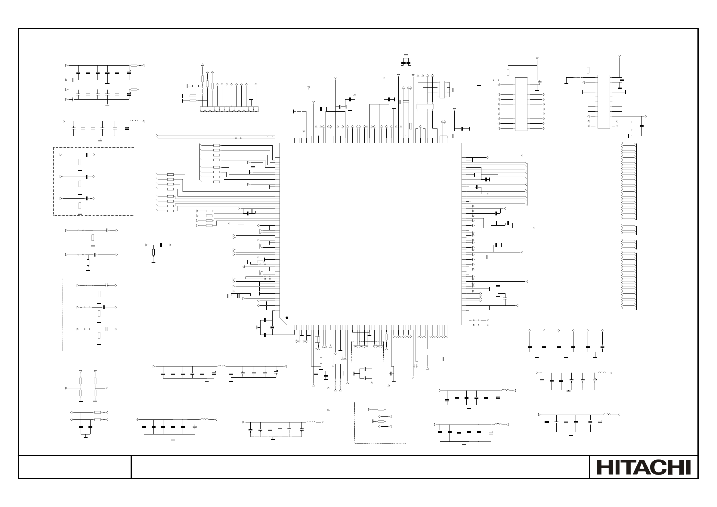
PAVDD1
PAVDD2
PDVDD
GIN2
BIN2
RIN2
C_SELECTED
CVBS_SVP
MPUCSON
20
VCC
10
GND
11
B8
12
B7
13
B6
14
B5
74HC245
15
B4
16
B3
17
B2
18
B1
VDDMQ_2V5
MA[0-11]
VD1_8
VDDMQ_2V5
VREFP_1
C450
AVDD_ADC3
AVDD_ADC1
16V
100n
VCCA_3V3
VDDMQ_2V5
C2231
3k3
R2240
S448
16V
100n
C2405
DIN[7]
DIN[6]
DIN[5]
DIN[4]
DIN[3]
DIN[2]
DIN[1]
DIN[0]
VREFN_1
16V
100n
C457
16V
100n
C2232
16V
100n
C2239
C2240
DE_PING
CLK_2EX_PING
ODD_PINK_PING DVS_2EX
DHS_2EX_PING
VREFP_2
VREFN_2
16V
16V
100n
100n
C462
C460
16V
C2233
100n
16V
100n
C2234
16V
100n
16V
100n
100n
C2242
C2241
16V
100n
IC400
1
DIR
19
G
9
A8
8
A7
7
A6
6
A5
5
A4
4
A3
3
A2
2
A1
VREFP_3
16V
100n
C463
C467
2u2
L404
10u
16V
16V
100n
C442
C445
330R_100MHZ_3A
10u
16V
16V
16V
100n
C454
R435
VL1_8
22R
10u
16V
16V
100n
C2206
C438
MLF1
2n7
50V
16V
100n
C2207
PLF2
2n7
50V
C439
16V
100n
C2216
C2217
75R
R406
75R
R407
75R
R408
16V
16V
100n
100n
C440
C2203
16V
16V
100n
100n
C2209
C2208
16V
16V
100n
100n
C2219
C2218
C403
Y_G2
100n
16V
C404
PB_B2
100n
16V
C405
PR_R2
100n
16V
PC & Y PbPr INPUT
S430
75R
R401
C402
S431
100n
16V
75R
R402
C406
RGB_GIN
RGB_RIN
RGB_BIN
S425
75R
R403
S426
100n
16V
C407
75R
R404
S427
C408
75R
R405
16V
16V
100n
100n
C2204
C2205
16V
100n
C2210
C2211
16V
100n
C455
C401
100n
100n
16V
100n
16V
100n
C
CVBS3
Y_G1
PR_R1
PB_B1
16V
100n
16V
16V
16V
330R_100MHZ_3A
10u
C444
R436
22R
10u
C443
L407
C459
MAIN PICTURE
CVBS_SVP
VL1_8
MCA[14]
MCA[15]
MCA[0]
MCA[0-19]
MCA[1]
MCA[2]
MCA[3]
MCA[4]
MCA[5]
MCA[6]
MCA[7]
C400
100n
16V
75R
R400
R2230
R2229
R2228
R2227
R2226
R2225
R2224
R2223
100R
100R
100R
100R
100R
100R
100R
100R
CVBS2
MAIN RGB INPUT
VDDL
16V
16V
100n
100n
C2212
VDDH
16V
16V
100n
100n
C2221
C2220
C2254
C2214
C2213
16V
16V
100n
100n
C421
C2222
SDA_EX
SCL_EX
C410
R423
R424
VCCA_3V3
10k
1k
68p
VCCA_3V3
10k
R425
MPUGPIO4
10k
R426
R413
SDA3
68R
R414
SCL3
68R
68p
C412
CLK_2EX_PING
ODD_PINK_PING
DHS_2EX_PING
22R
R431
D_PING[7]
D_PING[6]
D_PING[5]
D_PING[7]
4
D_PING[6]
5
D_PING[5]
6
D_PING[4]
D_PING[4]
7
R2210
R432
10k
R433
10k
PL104
22R
R430
10k
22R
R429
S110
1
3
2
DIGITAL IDTV INPUTS [ITU 601]
R2231
MCAD[0]
100R
R2232
MCAD[1]
100R
R2233
MCAD[2]
100R
R2234
MCAD[3]
100R
MCAD[0-7]
R2235
MCAD[4]
100R
R2236
MCAD[5]
100R
R2237
MCAD[6]
100R
R2238
MCAD[7]
100R
L401
C433
VCCA_3V3
INT#
PR_R1
PR_R2
PB_B2
CVBS2
CVBS3
VD1_8
R244
C
PB_B1
AVDD_ADC1
Y_G1
Y_G2
C409
C2400
AVDD3_AVSP2
100n
RD_EMU
WR_EMU
ALE_EMU
MPUCSON
16V
100n
16V
100n
C2215
R2222
R2221
100R
R2220
100R
R2219
100R
330R_100MHZ_3A
10u
16V
16V
16V
100n
100n
C431
150R 600mA
L400
10u
16V
C423
D_PING[3]
D_PING[3]
8
S411
STBY_3V3
100R
VD1_8
16V
D_PING[2]
D_PING[2]
D_PING[1]
9
VD1_8
100n
C411
AVDD_ADC3
AVDD_ADC2
AVDD3_AVSP2
100n
100n
C2401
D_PING[1]
10
C413
VREFN_3
VREFP_3
VREFN_2
VREFP_2
VREFN_1
VREFP_1
PDVDD
PAVDD
16V
C2223
11
R427
C2402
D_PING[0]
16V
100n
D_PING[0]
12
16V
100n
75R
16V
100n
C2224
100n
100n
C434
C435
VD1_8
VD1_8
RAS#
CAS#
CS0#
R2216
MD[16]
MD16
DIN[16]
147
BA1
33R
BA1
DIN[15]
146
VSSC7
DIN[14]
BA0
145
BA0
DIN[13]
R2215
144
CLKE
33R
CLKE
DIN[12]
VDDC7
100n
16V
C436
VDDH
R2213
142WE143
WE#
765
8
R1R2R3
123
MVREF
139
140
141
VSSR
VDDR
MVREF
DIN[9]
DIN[10]
DIN[11]
R4
4
134
135
136
137
138
CS1
RAS
CAS
VDDM10
DIN856CLK
DIN758DIN659DIN560DIN461DIN362DIN263DIN164DIN0
55
57
DIN[8]
DIN[7]
DIN[6]
33R
R2217
R2218
33R
CLK_2EX
AVDD_ADC2
PAVDD
VDDM9
DIN[5]
133
1
2
3
4
CS0_
DIN[4]
C2235
R2214
132
VSSM10
DIN[3]
8
R1
7
R2
6
R3
5
R4
VDDMQ_2V5
MCLK0
MCLK0#
C437
100n
16V
131
129
130
MCK0
VSSM9
MCK0_
128
VDDL
127
VSSL
126
MA0
125
MA1
124
VDDM8
123
MA2
122
MA3
121
VSSM8
120
MA4
119
VDDM7
118
MA5
117
MA6
116
VSSM7
115
MA7
114
MA8
113
VDDC6
112
MA9
111
MA10
110
VSSC6
109
MA11
108
MD15
107
VDDC5
106
MD14
105
VSSM6
104
MD13
103
VDDM6
102
MD12
101
VSSM5
100
DQS1
99
VDDM5
98
VSSM4
97
DQM1
96
MD11
95
VDDM4
94
MD10
93
MD9
92
VSSC5
91
MD8
90
MD7
89
VDDC4
88
MD6
87
VSSM3
86
MD5
85
VDDM3
84
MD4
83
VSSM2
82
DQS0
81
VDDM2
80
VSSM1
79
DQM0
78
MD3
77
VDDM1
76
MD2
75
MD1
74
VSSC4
73
MD0
72
DIN20
71
DIN21
70
DIN22
69
DIN23
68
VSSC3
67
VDDC3
66
VSSH3
65
VDDH3
DIN[2]
DIN[1]
DIN[0]
16V
100n
C2229
C2228
16V
100n
C2227
100n
100n
C2236
C2237
C2238
100n
DE_PING
D_PING[7]
D_PING[6]
D_PING[5]
D_PING[4]
D_PING[3]
D_PING[2]
D_PING[1]
D_PING[0]
VDDL
C447
16V100n
C446
100n
16V
VD1_8
MD[15]
MD[14]
MD[13]
MD[12]
DQS[1]
DQM[1]
MD[11]
MD[10]
MD[9]
MD[8]
MD[7]
MD[6]
MD[5]
MD[4]
DQS[0]
DQM[0]
MD[3]
MD[2]
MD[1]
MD[0]
DIN[20]
DIN[21]
DIN[22]
DIN[23]
VDDH
S446
STBY_3V3
S445
16V
16V
100n
100n
100n
C465
C2230
330R_100MHZ_3A
100n
100n
C466
10u
VDDMQ_2V5
STBY_3V3
VD1_8
C425
MD[30]
MD30
4k7
MD[29]
180
MD29
RST_H
R420
C422
178
179
VDDM16
SCL_EX
D101
VCCA_3V3
MD[28]
177
MD28
100n
STBY_5V
DQM[3]
DQM3
SDA_EX
16V
1N4148
16V
100n
100n
C424
16V
MD[22]
MD[23]
MD[24]
MD[25]
MD[26]
MD[27]
DQS[3]
172
173
174
175
176
171
DQS3
MD27
VSSM15
VSSM16
VDDM15
VDDM14
163
164
165
166
167
168
169
170
MD23
MD25
MD22
MD26
MD24
VSSC8
VDDC9
VSSM14
IC224
SVP_EX_51
TXOUT3-
TXOUT3+
TXOUT2+
TXCLKOUT-
TXCLKOUT+
LVDS OUT
PARITY
DHS_2EX
PWM2
S443
S444
DIGITAL SINC
VDDH
STBY_3V3
DVS_2EX
DE_2EX
VCCA_3V3
C426
100n
C427
100n
TXCLKOUT+
TXCLKOUT-
VD1_8
188
189
MPUGPIO3
MPUGPIO4
187
VSSH4
MPUGPIO4
PLF2
PAVDD2
C432
186
VDDH4
L402
C418
100n
16V
MD[31]
181
182
183
184
185
MD31
VSSC9
VSSC10
VDDC10
R418
R419
22R
22R
VGA_VSIN
VGA_HSIN
16V
100n
C420
VD1_8
S437
S413
190
191
192
NC
MPUGPIO1
193
MPUGPIO0
194
A_D0
195
A_D1
196
A_D2
197
A_D3
198
VDDC12
199
VSSC12
200
A_D4
201
A_D5
202
A_D6
203
A_D7
204
VDDH5
205
VSSH5
206
ADDR0
207
ADDR1
208
ADDR2
209
ADDR3
210
ADDR4
211
ADDR5
212
ADDR6
213
ADDR7
214
VDDC11
215
VSSC11
216
RD
217
WR
218
ALE
219
MPUCSON
220
INT
221
AVDD_ADC3
222
AVSS_ADC3
223
VREFN_3
224
VREFP_3
225
PR_R1
226
PR_R2
227
AVDD_ADC2
228
AVSS_ADC2
229
VREFN_2
230
VREFP_2
231
C
232
PB_B1
233
PB_B2
234
AVDD3_AVSP2
235
AVSS3_BG_ASS
236
CVBS_OUTP
237
50V
20p
C414
50V
20p
C415
C2403
CVBS_OUTN
238
AVDD_ADC1
239
AVSS_ADC1
240
VREFN_1
241
VREFP_1
S439
242
CVBS1
243
CVBS2
244
S438
CVBS3
245
AIN_N1
246
Y_G1
247
AIN_N2
248
Y_G2
249
AIN_N3
250
VSSC13
251
VDDC13
252
PDVDD
253
PDVSS
254
PAVDD
255
PAVSS
256
XTALI
X400
14.31818MHz
10u
16V
C2404
16V
100n
16V
16V
100n
100n
C2226
C2225
S441
MPUGPIO2
MLF1
PAVDD1
VD1_8
330R_100MHZ_3A
10u
16V
16V
16V
100n
100n
C430
VDDMQ_2V5
C428
100n
MD[18]
MD[19]
MD[20]
MD[21]
DQM[2]
DQS[2]
152
153
154
155
156
157
158
159
160
161
162
MD21
DQS2
MD19
TXOUT2-
VDDM13
MD20
VCCA_3V3
MD18
DQM2
VSSM13
VSSM12
VDDM11
VDDM12
TB1-36TA1+
TB1+33LVDSV CC32LVDSG ND31TC1-30TC1+29TCLK-28TCLK+27TD1-26TD1+25PLL_GND24PLL_VCC23DE22V21H20VSSH119VDDH118FLD_IO17PWM16SDA15V5SF14SCL13RESET12TESTMODE11AIN_VS10AIN_HS9VDDC18VSSC17PAVSS26PLF25PAVDD24PAVSS13MLF12PAVDD11XTALO
TA1-38LVDSVDDP39GPO40VDDC241VSSC242DIN1943DIN1844DIN1745DIN1646DIN1547DIN1448DIN1349DIN1250VDDH251VSSH252DIN1153DIN1054DIN9
35
34
37
10k
R422
TXOUT1-
TXOUT0-
TXOUT1+
TXOUT0+
VCCA_3V3
C429
100n
16V
VD1_8
R2211
10k
TXCLKOUT+
R2212
10k
TXCLKOUT-
151
VSSM11
DIN[19]
150
MD[17]
MD17
DIN[18]
149
VDDC8
DIN[17]
148
CMO PANEL OPTION
S447
C448
100n
16V
C449
100n
16V
C451
10u
16V
16V
L408
C469
VD1_8
16V
100n
C456
16V
100n
330R_100MHZ_3A
L409
C468
3k3
R2239
IC401
1
DIR
19
G
9
A8
8
A7
7
A6
6
A5
5
A4
4
A3
3
A2
2
A1
MA[0]
MA[1]
MA[2]
MA[3]
MA[4]
MA[5]
MA[6]
MA[7]
MA[8]
MA[9]
MA[10]
MA[11]
100n
C452
VD1_8
VA1_8
VL1_8
VCC
GND
B8
B7
B6
B5
74HC245
B4
B3
B2
B1
VREFN_3
16V
100n
L406
C458
VCCA_3V3
20
16V
MD[0]
MD[1]
MD[2]
MD[3]
MD[4]
MD[5]
MD[6]
MD[7]
MD[8]
MD[9]
MD[10]
MD[11]
MD[12]
MD[13]
MD[14]
MD[15]
MD[16]
MD[17]
MD[18]
MD[19]
MD[20]
MD[21]
MD[22]
MD[23]
MD[24]
MD[25]
MD[26]
MD[27]
MD[28]
MD[29]
MD[30]
MD[31]
DQM[0]
DQM[1]
DQM[2]
DQM[3]
DQS[0]
DQS[1]
DQS[2]
DQS[3]
DIN[0]
DIN[1]
DIN[2]
DIN[3]
DIN[4]
DIN[5]
DIN[6]
DIN[7]
DIN[8]
DIN[9]
DIN[10]
DIN[11]
DIN[12]
DIN[13]
DIN[14]
DIN[15]
DIN[16]
DIN[17]
DIN[18]
DIN[19]
DIN[20]
DIN[21]
DIN[22]
DIN[23]
VA1_8
DHS_2EX
VA1_8
C2406
100n
10k
50V
R2241
DQM[0-3]
DQS[0-3]
CLK_2EX
18p
C2407
DIN[0-23]
10
11
12
13
14
15
16
17
18
No. 0232
TFT TV Service Manual
MAIN BOARD (17MB15E-7) - SHEET 4
49
Page 54
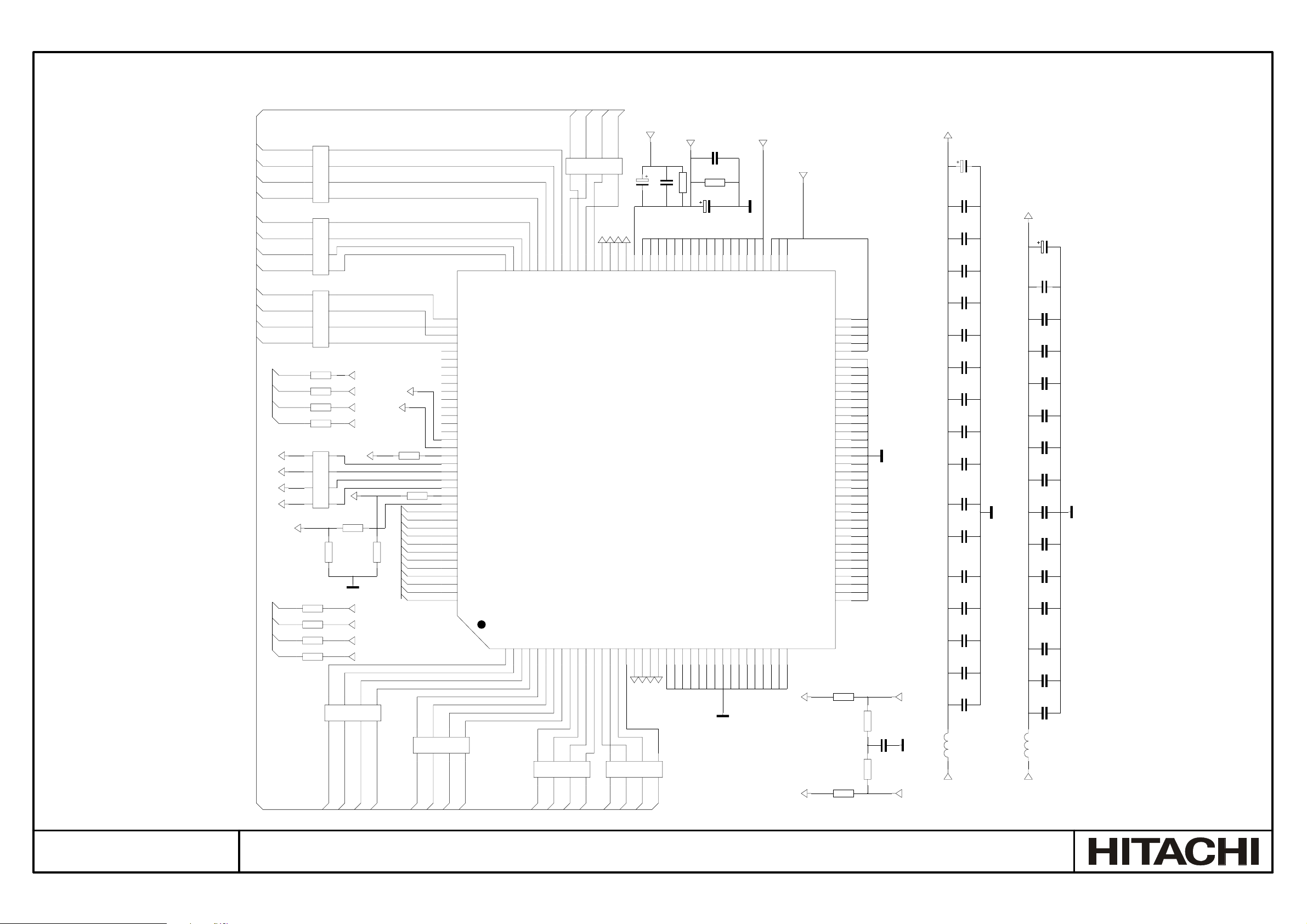
MD[27]
MD[26]
MD[25]
MD[24]
MD[23]
MD[22]
MD[21]
MD[0-31]
MD[20]
MD[19]
MD[18]
MD[17]
MD[16]
DQS[0]
DQS[1]
DQS[2]
DQS[0-3]
DQS[3]
WE#
CAS#
RAS#
CS0#
BA1
DQM[0-3]
1
2
3
4
1
2
3
4
1
2
3
4
1
2
3
4
R522
R523
R524
R525
R500
10R
R1
R2
R3
R4
R501
10R
R1
R2
R3
R4
R502
10R
R1
R2
R3
R4
R513
15R
R514
15R
R515
15R
R516
15R
R503
R1
R2
R3
R4
R506
R520
8
10R
1
MD[15]
8
7
6
5
8
7
6
5
8
7
6
5
8
7
6
5
R1
33R
CLKE
R519
33R
7
R2
2
MD[14]
DDQS0
DDQS1
DDQS2
DDQS3
BA0
R521
DDQM[0]
DDQM[1]
DDQM[2]
DDQM[3]
6
R3
3
MD[13]
MCLK01
R518
33R
5
R4
4
MD[12]
MCLK01#
R517
33R
33R
MA[11]
MA[10]
MA[9]
MA[8]
MA[7]
MA[6]
MA[5]
MA[4]
MA[3]
MA[0-11]
MA[2]
MA[1]
MA[0]
8
10R
R1
R507
1
MD[11]
7
R2
2
MD[10]
20
22
82
120
119
123
134
122
75
15
116
129
131
130
143
110
109
121
133
135
124
126
113
127
142
141
140
128
139
138
125
137
136
3
MD[9]
9
8
7
6
R3
DQ28_A9
DQ29_A8
DQ30_B8
DQ31_A7
NC_B10
NC_G10
NC_K12
NC_K11
NC_L3
NC_M2
NC_L2
NC_G3
NC_B3
NC_K8
NC_L9
CK-_L11
CK_L10
CKE_M11
WE-_K2
CAS-_K1
RAS-_L1
CS-_M1
BA0_M3
BA1_L4
A11_L6
A10_K5
A9_L7
A8/AP_M10
A7_M9
A6_M8
A5_L8
A4_M7
A3_M6
A2_L5
A1_M5
A0_M4
5
R4
4
MD[8]
35
24
DQ26_C11
DQ27_B12
DQ1_B5
DQ0_A6
6
17
59
48
36
DQ25_C12
DQ24_D12
DQ2_A5
DQ3_A413DQ4_B1
5
4
8
10R
R509
1
MD[7]
72
71
60
DQ13_F11
DQ12_F12
DQ15_E11
DQ14_E12
DQ5_C225DQ6_C137DQ7_D150DQ16_E2
26
7
R1
R2
2
3
MD[6]
MD[28]
4
R4
5
107
96
95
DQ11_H11
DQ10_H12
DQ17_E162DQ18_F261DQ19_F1
49
6
5
R3
4
MD[5]
MD[4]
MD[31]
MD[30]
MD[29]
18
2
3
R1
R3
R2
10R
R508
7
6
11
108
DQ9_J11
DQ8_J12
DDQM[2]
DDQM[3]
12
83
DM3_A11
DM1_G11
1u
DDQS2
DDQS3
144
84
VREF_M12
DQS3_A12
DQS1_G12
14
EM6A9320
IC1
DQ20_H285DQ21_H197DQ22_J198DQ23_J22DM0_A274DM2_G21DQS0_A173DQS2_G1
86
DDQM[1]
7
8
R4
10R
R511
MD[3]
6
R1
R2
1
2
3
MD[1]
MD[2]
VDDMQ_2V5_FLT
C501
18
16
VDDQ_B2
VDDQ_B6
VDDQ_B4
DDQS1
DDQS0
DDQM[0]
5
R3
R4
4
MD[0]
MVREF
R510
1k
100n
19
132
C502
C517
1u
50V
47
38
23
21
VDDQ_B9
VDDQ_B7
VDDQ_D2
VDDQ_B11
VDDQ_D11
NC_L123VSSQ_A310VSSQ_A1027VSSQ_C328VSSQ_C4
100n
C518
R512
1k
87
63
51
VDDQ_F3
VDDQ_E3
VDDQ_H3
VSSQ_C532VSSQ_C833VSSQ_C9
29
VDDMQ_2V5_FLT
106
94
70
58
99
VDDQ_J3
34
VDDQ_J10
VDDQ_F10
VDDQ_E10
VDDQ_H10
VSSQ_C1041VSSQ_D544VSSQ_D852VSSQ_E457VSSQ_E9
30
31
VDD_C7
VSSQ_F469VSSQ_F9
64
MCLK0
MCLK0#
46
VDD_C6
VDD_D10
VSSQ_G4
76
VCCA_2V5_FLT
VDD_D3
VDD_K10
VDD_K7
VDD_K6
VDD_K3
VSS_H8
VSS_H7
VSS_H6
VSS_H5
VSS_G8
VSS_G7
VSS_G6
VSS_G5
VSS_F8
VSS_F7
VSS_F6
VSS_F5
VSS_E8
VSS_E7
VSS_E6
VSS_E5
VSS_D9
VSS_D7
VSS_D6
VSS_D4
VSS_J8
VSS_J7
VSS_J6
VSS_J5
VSS_K9
VSS_K4
VSQ_J9
VSSQ_H9
VSSQ_J4
VSSQ_H4
VSSQ_G9
39
118
115
114
111
92
91
90
89
80
79
78
77
68
67
66
65
56
55
54
53
45
43
42
40
104
103
102
101
117
112
105
93
100
88
81
R2209
10R
R2208
10R
R504
R505
47R
47R
C500
10n
25V
MCLK01
MCLK01#
VDDMQ_2V5_FLT
L501
C505
100u
16V
50V
4n7
C525
50V
4n7
C524
50V
4n7
C523
50V
4n7
C522
50V
4n7
C521
50V
4n7
C506
50V
4n7
C507
25V
10n
C508
25V
10n
C509
25V
10n
C510
25V
10n
C511
25V
10n
C512
25V
10n
C513
25V
10n
C514
25V
10n
C519
25V
10n
C520
BLM21B201S
VDDMQ_2V5
VCCA_2V5_FLT
C516
100u
100n
C532
100n
C531
100n
C530
100n
C529
100n
C528
100n
C527
100n
C515
100n
C504
100n
C503
100n
C2253
100n
C2252
100n
C2251
100n
C2250
100n
C526
L500
BLM21B201S
VCCA_2V5
16V
16V
16V
16V
16V
16V
16V
16V
16V
16V
16V
16V
16V
16V
16V
No. 0232
TFT TV Service Manual
MAIN BOARD (17MB15E-7) - SHEET 5
50
Page 55
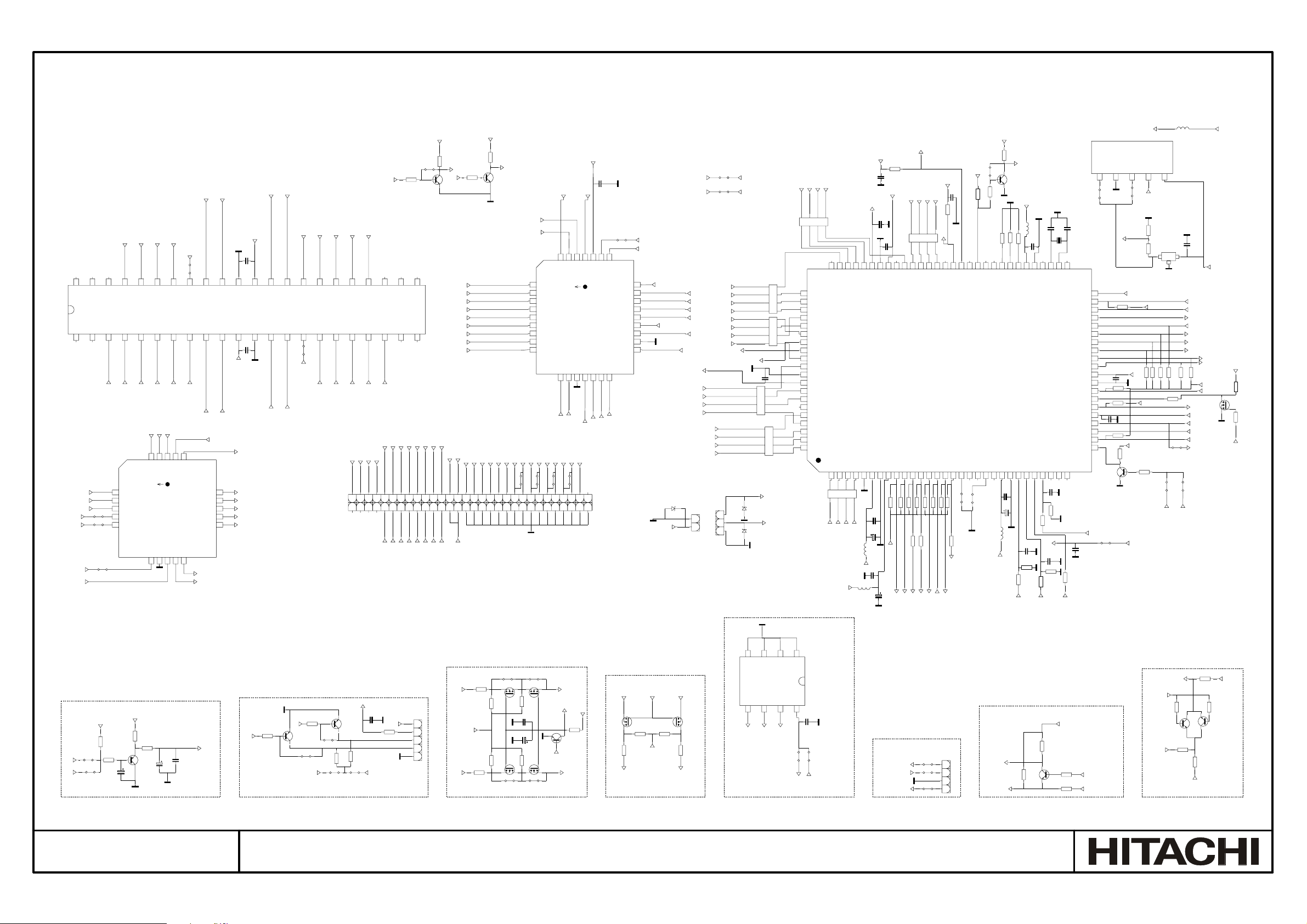
RD_EMU
WR_EMU
PSEN_UP
GAL_IAP
MCA[17]
MCA[18]
MCA[19]
EX_WDI
100k
4k7
VCCD_3V3
4k7
L609
BLM21B201S
C631
IC221
3
2
LM809
1
4k7
4k7
4k7
4k7
R682
R681
R680
R6017
4k7
R6041
S6314
S614
S613
FB
SC2_FB
25V
100n
PDP_GO1/BL_ON_OFF
INT#
GAL_IAP
UP_IRQ
NVM_WP
SCL3
SDA3
LED1
PWM
4k7
R6044
STBY_3V3
UP_RXD
Q6012
BSN20
LED2
PROTECT
SDA_TVLINK
IR1
UP_TXD
HDMI_CEC
STBY_3V3
VCCD_3V3
R6045
STBY_3V3
4k7
4k7
R6046
P1_CBL5V
STBY_3V3
4k7
R6035
PDP_GO/BL_ON_OFF
S600
MCA[16]
8
7
25
NC7
20 A9
MCA[9]
MCAD[0]
10
9
MCA[0]
MCAD[1]
12
11
MCA[1]
R6037
1k
BC848B
Q6009
23
24
NC5
NC6
21 NC3
22 NC4
MCAD[2]
MCAD[3]
MCAD[4]
MCAD[5]
14
13
1516171819202122232425 26
MCA[3]
MCA[2]
MCA[4]
MCA[5]
CPU_GO1/STBY
MCA[7]
MCA[6]
MCA[5]
MCA[4]
MCA[3]
MCA[2]
MCA[1]
MCA[0]
MCAD[0] MCAD[7]
MCAD[7]
MCAD[6]
MCA[8]
MCA[7]
MCA[6]
PDP_GO1/BL_ON_OFF
MCAD[5]
STBY_3V3
33
VCC1
12 VSS
32
I/O6
13 I/O3
MCAD[2]
MCAD[4]
31
I/O5
14 I/O4
MCAD[3]
S624
MCA[14]
30
A14
15 WE
SRAM_WE
MCA[13]
29
A13
16 A5
MCA[5]
PL607
MCA[12]
28
A12
17 A6
MCA[6]
MCA[11]
27
A11
18 A7
MCA[7]
MCA[19]
2
1
MCA[18]
4
3
MCA[10]
26
A10
19 A8
MCA[8]
MCA[17]
2
5
MCAD[7]
MCAD[6]
MCA[19]
MCA[18]
MCA[17]
MCA[16]
SRAM_OE
S623
42
43
44
NC10
1NC1
41
NC9
NC8
3A0
2NC2
4A1
MCA[0]
MCA[1]
4I2
5I3
6I4
S620
7I5
S621
8I6
S622
A18
39
40
A17
A16
5A2
6A3
MCA[2]
MCA[3]
MCA[16]
I1
IC622
GAL16LV8
I710GND11OE12Q013Q1
9
MCA[15]
2I03
MCA[4]
MCA[14]
1
CLK
36
37OE38
A15
I/O8
9I/O1
7A4
8AS
MCA[15]
MCAD[0]
STBY_3V3
19Q720
VCC
FL_A15
FL_A14
16V
100n
C601
34
35
I/O7
VSS1
IC217
K6R4008V1C-I/C-P
11 VCC
10 I/O2
C600
100n
16V
STBY_3V3
MCAD[1]
FL_WE
FL_OE
18Q6
SRAM_WE
17Q5
SRAM_OE
16Q4
FL_A17
15Q3
FL_A16
14Q2
STBY_3V3
4k7
R6036
MCA[11]
MCA[12]
Q6008
BC848B
MCA[13]
CPU_GO
MCA[14]
R6038
1k
MCA[9]
MCA[10]
272829303132333435363738394041 42
STBY_3V3
FL_A16
FL_A15
A7
5
A6
6
A5
7
A4
8
A3
9
A2
10
A1
11
A0
12
DQ0
13
RD_EMU
FL_OE
MCA[15]
PSEN_UP
SRAM_OE
SRAM_WE
S6319
S6320
4344454647484950515253545556575859
MCA[12]
4
3
A15
A12
M29W040B
CORRESPONDS TO
Winbound W27E040 EPROM &
ST M29F040 Flash
DQ115DQ216VSS
14
MCAD[2]
MCAD[1]
RST#
STBY_3V3
WR_EMU
S6317
S6318
2
A16
IC219
ALE_EMU
STBY_3V3
100n
25V
MCA[18]
1
32
A18
VCC
DQ318DQ419DQ5
17
MCAD[4]
MCAD[3]
60
C605
31
W
MCAD[5]
30
A17
DQ6
20
MCAD[6]
R632
4k7
STBY_2V5
73VDD2_5_1
8 VDD3_3
4k7
STBY_3V3
72FL_PGM
9P0_0
SDA2
R1R2R3
10R
R639
18234
71A15
10 P0_1
4k7
4k7
R689
R6013
R6030
SCL2
MCA[17]
47R
DE_PING
765
70A17
11 P0_2
4k7
R690
R6031
WR_EMU
MCA[16]
MCA[18]
MCA[19]
R4
69A16
68A18
IC220
SDA5550M
12 P0_3
13 P0_4
4k7
4k7
R695
R694
47R
RX1_RST#
MUTE_AMP
67A19
14 P0_5
RX1_INT
STBY_3V3
R640
RD_EMU
66NC5
15 P0_6
3k9
4k7
R697
R696
CPU_GO1/STBY
100n
C615
4k7
63NC4
64WR
65RD
17 ENE
18 STOP
16 P0_7
S610
S615
15k
R698
EX_WDI
STBY_3V3
79A7
2D4
R3
MCAD[4]
78A13
3D2
R2
765
MCAD[2]
77A12
4D3
1823
R1
MCAD[3]
L600
BLM21B201S
L601
C610
100n
16V
C609
VCCD3.3V_FLT
100n
25V
25V
100n
C612
75VDD3_3_2
76A14
74VSS2
5XROM
7VSS
6 VDD2_5
R688
25V
100n
C608
C607
22u
50V
STBY_2V5
100n
C613
C611
22u
S607
SDA2
SCL2
S604
FL_WE
FL_A17
FL_A14
A14
29
A13
28
A8
27
A9
26
A11
25
G
24
A10
23
E
22
DQ7
21
LOC_KEY
FL_OE
D600
BZT55C5V1
VCCD3.3V_FLT
MCA[10]
MCA[2]
MCA[1]
MCA[0]
PL606
MCA[13]
MCA[8]
MCA[9]
MCA[11]
MCA[10]
MCAD[7]
MCAD[6]
MCAD[0]
MCAD[5]
2
1
PL604
MCA[7]
MCA[8]
MCA[6]
MCA[9]
MCA[4]
MCA[11]
MCA[5]
MCA[3]
1
2
3
SDA3
S608
SCL3
7
6
5
7
6
ALE_EMU
D601D602
5
25V
100n
R4
4
5
R3
6
3
R2
2
7
R1
18
10R
R625
R624
10R
1
R1
2
R2
3
R3
4
R4
SCL
PSEN_UP
MCA[13]
MCA[12]
MCA[14]
MCA[15]
765
R1R2R3
R4
10R
R629
18234
80FL_RST
R627
10R
18
R1
2
81 A8
R2
3
82 A6
R3
4
83 A9
R4
18
84 A5
R1
2
85 A11
R2
3
86 A4
R3
4
87 ALE
R4
R626
88 PSEN
10R
89 A3
90 A10
91 VSS3
C606
92 VDD3_3_3
93 A2
94 A1
95 FL_CE
96 D7
97 A0
8
98 D6
7
99 D0
6
100 D5
5
1D1
4
R4
10R
R628
SDA
MCAD[1]
STBY_3V3
R648
STBY_3V3
4k7
62P1_7
19 OCF
STBY_3V3
4k7
R6043
RST_H
S601
Q6011
BC848B
1k
R6042
20 EXTIF 61NC3
60
BLANK_COR
R684
21 CVBS
STBY_2V5
75R
25V
100n
C621
C620
59B
R685
22 VDDA2_5
22u
50V
L603
STBY_2V5
57R
58G
33p
33p
50V
50V
C627
C624
L604
6MHz
25V
75R
75R
100n
R686
23 VSSA
24 P2_0
15k
PIN8_SC1
C623
25V
100n
C622
R653
3k9
R654
56VDDA2_5_1
25 P2_1
X600
51NC1
53XTAL1
55VSSA1
52XTAL2
54NC2
50RST
49P4_3
48P4_2
47P1_6
46P1_5
45P1_4
44P1_3
43P1_2
42P1_1
41P1_0
40VDD3_3_1
39VSS1
38P3_7
37P3_6
36P3_5
35P3_4
26 P2_2
27 P2_3
28 NC
25V
100n
C626
3k9
R657
15k
R656
LOC_KEY
25V
100n
C625
3k9
R660
15k
R655
PIN8_SC2
34P3_3
29 HS_SSC
30 VS
33P3_2
32P3_1
31P3_0
PIN8_SC3
C628
100n
25V
1k
R661
STBY_2V5
VCCD3.3V_FLT
IC623
STM6321
RST-2VSS3RST4MR-5VCC
1
S6313
Q6010
BC848B
25V
100n
C633
RST#
R693
4k7
VCCD3.3V_FLT
100n
C630
R691
4k7
R6014
4k7
R692
4k7
4k7
R6040
S6321
RST#
VCCA_2V5
PC_STBY
R6039
100R
R687
R676
R679
STBY_3V3
S6322
VCCA_2V5
1k2
R415
S412
PWM
S414
PWM2
VCC_5V
4k7
R416
R417
R412
22R
22R
BC327
Q400
16V
10u
50V
100u
C416
No. 0232
TFT TV Service Manual
BRIGHTNESS
CONTROL
DIMMING
16V
100n
C419
C417
BRT_CNTL
R6018
LED1
BC848B
Q6007
22k
S6310
STBY_5V
R6019
LED2
22k
LED DRIVER CIRCUIT & IR INPUT
VSS
S605
S6315
Q604
SCSCL
IR
C634
100n
16V
STBY_3V3
STBY_5V
5
R604
4k7
4
3
2
1
PL600
STBY_5V 47k
SCSDA
BC848B
Q6006
S6300
220R
R6015
220R
R6016
S6311S6312
Q600
100R
R6006
100R
R6011
4k7
R600
10k
R6007
C635
16V
220n
10u
50V
C636
4k7
10k
R601
R6010
Q601
S606
S6316
CIRCUIT OF SW UPDATE FROM SCART2
SCL3
STBY_5V
HDMI_DDC_WP
R6005
Q606
BC846B
SW_ENABLE
Q605
SDA3
SCL3
BSN20
Q602
R607
10k
100R
R606
SCL
LEVEL SHIFTER
VCCA_3V3
STBY_5V
SDA3
BSN20
Q603
R610
10k
100R
R611
SDA
E2
IC218
24LC32A
SDA6SCL7WP8VCC
5
SDA2
1A02A13A24
SDA_TVLINK
STBY_3V3
47k
STBY_5V
TV-LINK
R2301
Q2300
BC848B
R2303
10k
16V
100n
NVM_WP
S603
STBY_3V3
C604
4k7
R603
BC848B
Q2299
4k7
R602
S602
VCCA_3V3
UART SOCKET FOR IDTV
PL308
S629
UP_RXD
UP_TXD
UP_IRQ
1
S628
2
3
S627
4
DMP_IR
IR1
SCL2
STBY_3V3
R2306
47k
R2305
100R
MMC_IR
DMP_IR_SW2
IR
STBY_3V3
2k7
R2300
47k
R2302
BC848B
Q2301
100R
R2304
TV_LINK
MAIN BOARD (17MB15E-7) - SHEET 6
51
Page 56
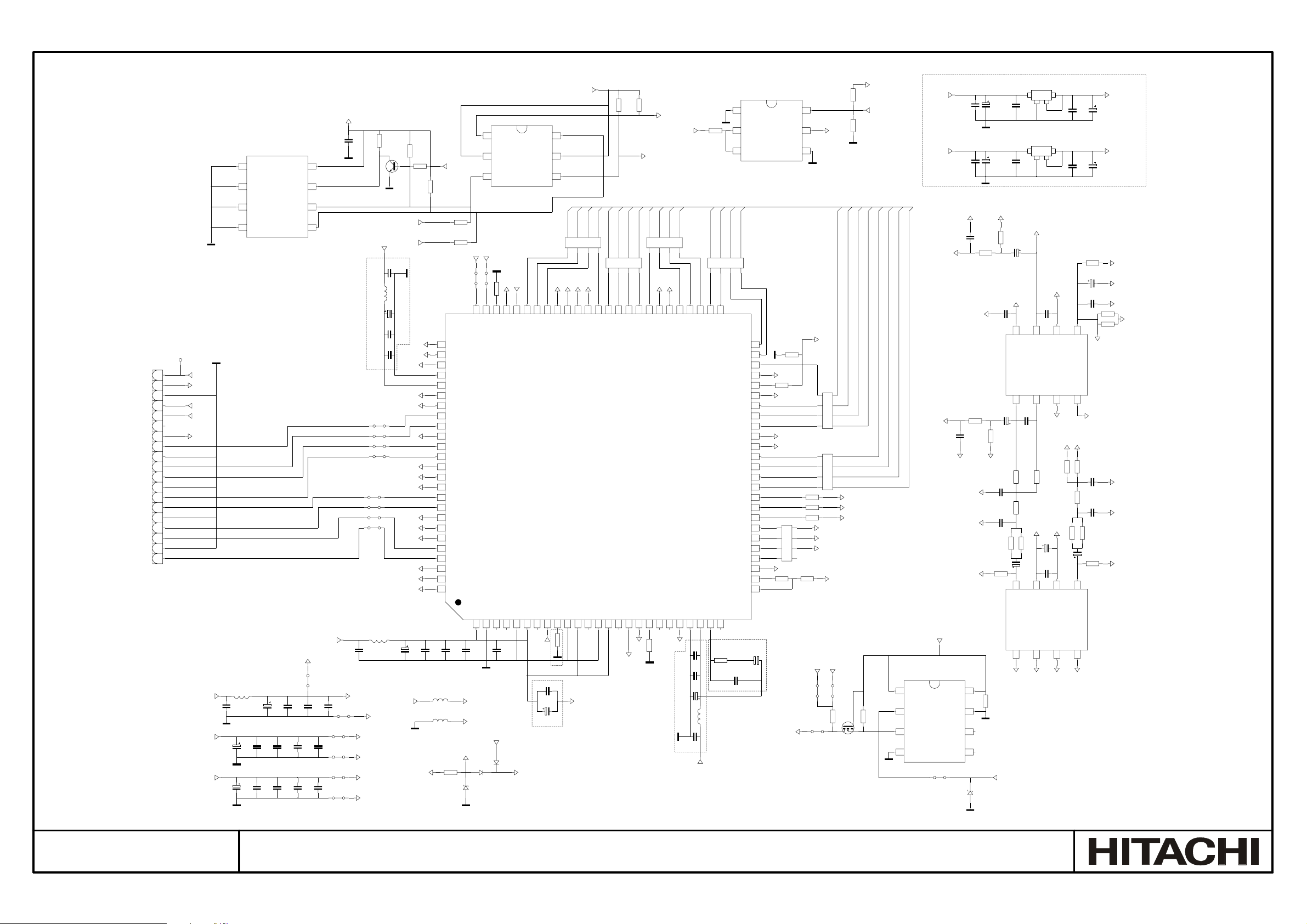
19
18
17
16
15
14
13
12
11
10
9
8
7
6
5
4
3
2
1
PL2001
TP100
P1_DDC_SDA
P1_DDC_SCL
HDMI_3V3
HDMI_3V3
HDMI_3V3
P1_HPD
P1_CBL5V
CEC
60R_100MHZ_3A
100n
C2073
10u
16V
10u
16V
L2015
C3002
C3007
AUDIO_AGND
C2101
10u
50V
25V
IC2008
50V
10u
R2078
2k32
IC2006
AUDIO_AVCC5
8H
A
1
5k6
4k7
R2077
R2075
8AOUTL
SDATA
1
DAC_SD0
100n
16V
100n
16V
C2093
270p
3
3
50V
2k32
R2076
3u3
50V
IC3000
LM1117
OUT
IN
2
VOUT
GND
1
4
IC3001
LM1117
OUT
IN
2
VOUT
GND
1
4
AMP_PIN7
AMP_PIN6
C2102
270p
50V
7G
6F
MC33202
B
C
2
3
AMP_PIN3
R2085
1k2
R2079
AUDIO_AVCC5
AUDIO_AGND
C2095
10u
50V
25V
100n
C2088
C2094
6
7
VA
AGND
CS4334
DEM/SCLK3LRCK4MCLK
2
DAC_WS
DAC_SCK
C3003
C3008
AMP_PIN6
1k2
R2086
2k32
R2082
C2096
100n
16V
100n
16V
5
E
D
4
AMP_PIN7
5k6
4k7
R2084
2k32
R2083
3u3
5
AOUTR
DAC_MCLK
C3004
100u
16V
C3009
100u
16V
R2091
20k
C2103
10u
50V
C2104
100n
25V
AUDIO_AGND
C2098
2n7
50V
C2097
2n7
50V
50V
R2074
270k
R2089
47k
R2090
47k
AMP_PIN3
HDMI_3V3_PLL
AUDIO_AGND
AUDIO_AGND
AUDIO_AGND
AUDIO_AVCC5
AUDIO_AGND
AUDIO_AGND
AUDIO_AGND
DIN[16]
2N7002
R2070
R2069
DE_2EX
DVS_2EX
DHS_2EX
Q1
1k
10k
DIN[17]
DIN[18]
R2096
P1_5V
P1_HPD
DIN[19]
DIN[20]
DIN[21]
VCC_5V
VCC_5V HDMI_3V3
C3005
DIN[22]
DIN[23]
DAC_AOR
AUDIO_AGND
DAC_AOL
C2091
AUDIO_AGND
AUDIO_AGND
AUDIO_AGND
HDMI_3V3
C3000
100n
16V
100n
16V
C2100
AUDIO_AGND
2n7
R2081
560R
C3001
100u
16V
C3006
100u
16V
AUDIO_AGND
2n7
50V
100k
R2088
560R
R2087
100n
C2099
C2092
50V
100k
R2080
AUDIO_AGND
C2090
2n7
50V
C2089
2n7
50V
R2073
270k
IC2014
A8
11OE
27k
21A
SN74CB3Q3305
31B
4A4 5
S806
8
10k
R2095
2OE
7
2B
6
2A
CEC
D2023
BZT55C5V6
HDMI_3V3
470k
470k
R2066
R2067
DSCL
DIN[0]
DIN[14]
DIN[15]
8
R1R2R3
33R
R2050
123
5
R4
4
59
60
58
Q7
Q8
Q6
VCC118RSVDL119RSVDO120RSVDO2
17
4k7
VCC_SII
GND_SII
DSDA
DIN[1]
7
OGND_SII
57
OGND3
R2038
0VCC_SII
VCC_5V 4k7
DIN[2]
DIN[3]
5
6
R4
4
55
56
54
Q9
Q10
OVCC3
PGND223PVCC224PLLIN
OVCC
21
22
50V
0VCC_SII
1n
C2062
25V
100n
C2063
50V
10u
C2064
L2013
C2065
100n
25V
R2068
DIN[4]
8
R1R2R3
33R
R2049
123
53
52
Q11
Q12
R2039
60R_100MHZ_3A
HDMI_3V3_PLL
DIN[5]
7
51
Q13
NC3
25
3k9
P1_EVCC5
4k7
25V
100n
C2054
AVCC_SII
R2062
C2071
S817
S816
S815
S814
S813
S812
S811
S810
L2012
60R_100MHZ_3A
25V
100n
AGND_SII
VCC_SII
GND_SII
0VCC_SII
OGND_SII
47k
R2063
R2098
100R
4k7
R2099
100 VCC4
100n
C2056
L2016
330R_100MHZ_3A
L2017
330R_100MHZ_3A
HDMI_DDC_WP
76 DSDA
77 DSCL
78 OGND5
79 PGND1
80 PVCC1
81 EXT_RES
82 AVCC
83 RXC-
84 RXC+
85 AGND1
86 RX0-
87 RX0+
88 AGND2
89 AVCC1
90 AGND3
91 RX1-
92 RX1+
93 AVCC2
94 AGND4
95 AVCC3
96 RX2-
97 RX2+
98 AGND5
99 GND4
100n
C2057
R2071
10R
R2064
56R
R2065
56R
Q2
BC848B
P1_DDC_SCL
HDMI_3V3_PLL
P1_DDC_SDA
25V
100n
C2068
L2014
60R_100MHZ_3A
C2069
10u
50V
C2070
100n
DSDA
25V
DSCL
1n
OGND_SII
50V
RX1_AVCC3
AVCC_SII
AGND_SII
AGND_SII
AVCC_SII
AGND_SII
AVCC_SII
AGND_SII
AVCC_SII
AGND_SII
GND_SII
VCC_SII
10u
C2055
VCC_5V AUDIO_AVCC5
P1_CBL5V
C2058
AUDIO_AGND
P1_5V
D2020
S818
1n
D2021
1N5817
BZT55C5V6
IC2003
A0
1
A1
2
VCC
WP
C2072
8
7
24LC02
A2
3
VSS
4
10u
16V
25V
100n
C2078
C2079
100n
C2083
C2084
SCL
6
SDA
5
HDMI_3V3
RX1_AVCC3
S805
1n
25V
25V
100n
C2074
C2076
C2075
1n
25V
25V
100n
C2081
C2080
1n
25V
25V
100n
C2086
C2085
50V
100n
C2077
S800
S801
1n
50V
50V
C2082
S802
S803
1n
50V
50V
C2087
S804
IC2012
1S1
UPA672T
2G1
3D2 4S2
SDA3
SCL3
S819
75
CSDA
DACVCC2DACGND3NC14NC25DACGNDR6DACVCCR7ANRPR8COMP9RSET10DACGNDG11DACVCCG
1
RX1_INT
RX1_RST#
4k7
R2053
71
73
72
74
INT
CSCL
RESET
RSVDL2
1n
C2059
VCC_5V
D2022
1N5817
P1_EVCC5
6D1
5G2
DIN[8]
DIN[9]
7
8
R1R2R3
33R
R2052
123
VCC_SII
GND_SII
0VCC_SII
OGND_SII
69Q170
Q0
TOCOMP
C2060
10n
25V
C2061
10u
16V
65
67
68
66
Q2
GND3
OVCC4
OGND4
IC2002
SII9993
100R
R2035
TOCOMP
DIN[10]
DIN[11]
DIN[12]
DIN[13]
5
6
R4
4
7
8
R1R2R3
33R
R2051
123
61
63
62
64
Q3
Q5
Q4
VCC3
ANGY13DACGNDB14DACVCCB15ANBPB16GND1
12
6
6
C2066
25V
47n
1S1
2G1
3D2
DIN[6]
5
4
DIN[7]
R4
IC2013
UPA672T
50Q14
49Q15
48Q16
47OVCC2
46ODCK
45OGND2
44Q17
43Q18
42Q19
41GND2
40VCC2
39Q20
38Q21
37Q22
36Q23
35DE
34VSYNC
33HSYNC
32SCK
31WS
30SDO
29SPDIF
28OGND1
27MCLKIN
26MCLKOUT
C2067
25V
10u
DIN[0-23]
0VCC_SII
R2048
33R
OGND_SII
GND_SII
VCC_SII
R2042
33R
1
R1
2
R2
3
R3
4
R4
OGND_SII
R2040
33R
HDMI_CEC
R2094
33R
D1
6
G2
5
RX1_RST#
S2
4
CLK_2EX
R2047
33R
8
1
R1
2
7
R2
3
6
R3
4
5
R4
R2046
33R
1
8
R1
2
7
R2
3
6
R3
4
5
R4
R2045
33R
R2044
33R
R2043
33R
8
DAC_SCK
7
DAC_WS
6
DAC_SD0
5
R2041
33R
DAC_MCLK
HDMI_3V3
VCC_5V
S808
S809
330k
R2097
S807
No. 0232
TFT TV Service Manual
MAIN BOARD (17MB15E-7) - SHEET 7
52
Page 57
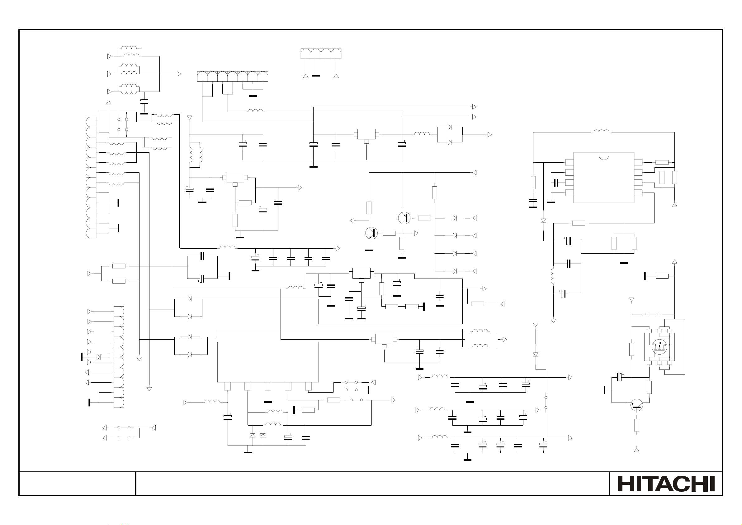
STBY_3V3
PDP_GO/BL_ON_OFF
A_DIM_PWM
DIG_DIM_PWM
PROTECT
CPU_GO1/STBY
VCC_33V
VCC_12V
DIG_DIM_PWM
VCC_12V
VCCA_3V3
1
2
3
4
5
6
7
8
9
10
11
12
PL900
SEL
A_DIM_PWM
D914
L928
L918
L926
L917
L927
5V
L900
L901
L902
L903
L904
R900
470R
R901
470R
S903
1
2
3
4
5
6
7
8
9
10
L906
S904
16V
100u
VCCA_3V3
5V
PL901
S900
S901
PANEL_VCC1
C900
L931
L905
L920
L930
VCCD_3V3
BRT_CNTL
VCC_12V
VCC_12V
+12V
C901
C903
D900
BA159_SMD
D901
BA159_SMD
D902
BA159_SMD
D903
BA159_SMD
PL902
1
L907
47u
50V
100n
47u
C902
L932
L908
22u
4
3
2
LM317
IC900
ADJ
C904
100n
16V
L919
22u
16V
1
1000u
5k6
5
R902
1k
R903
6
7
L909
50V
C908
C909
C912
100n
47u
C932
50V
100n
C906
2OUT3IN
16V
1000u
IC223
SAP 30030067 ADJ TYPE
LM2576
16V
1VIN
100u
C905
2 OUTPUT
22uH_3.9A_SMD
SS33
D911
3GND
L911
L910
22u
D904
STPS745
16V
C910
100n
16V
C933
1000u
STBY_5V
L912
4 FEEDBACK
C911
PL904
4
3
2
PDP_GO1/BL_ON_OFF
16V
220u
C914
VCC_8V
100n
100n
C934
C935
16V
100u
C931
5 ON/OFF
R904
330R
16V
100n
C913
1
LG_1/IRQPDP
PROTECT
100n
C915
100n
16V
16V
R905
160R
FAN1616AS-3.3
C916
100n
16V
BC848B
VCC_5V
CS52015-3
VIN
3
100n
50V
S905
S911
S902
SOT 223
Q900
IC901
VOUT
GND
C917
22u
IC902
1
1
R907
C918
10k
2
23
Q901
BC858B
R908
10k
120R
R909
120R
R911
SOT 223
IC903
LD1117
1
1.8V_ON/OFF
16V
220u
1.8V_ON/OFF
10k
R910
C919
100u
16V
23
1_8VMAIN
1_8VMAIN
1_8VMAIN
1_8VMAIN
C920
1R
R913
L913
C921
R912
10k
47u
R914
50V
L914
BA159_SMD
D905
D906
BA159_SMD
10k
C922
100n
16V
C923
100n
16V
L915
22u
22u
L916
22u
D907
1N4148
D908
1N4148
D909
1N4148
D910
1N4148
C925
C924
C926
BLM21B201S
BLM21B201S
16V
100n
16V
100n
16V
100n
STBY_5V
STBY_3V3
STBY_3V3
VCC_5V
VCCA_3V3
VCCD_3V3
VCC_8V
R915
470R
L921
L922
16V
100u
16V
100u
100u
STBY_2V5
VDDMQ_2V5
C936
C927
C937
C928
22u
C929
STBY_2V5
VCCA_2V5
16V
16V
100n
16V
16V
100n
C938
C930
100u
100u
C944
VD1_8
16V
100n
3k3
R922
1N4148
C939
C940
16V
100p
1N4148
STBY_2V5
D913
100u
L923
10u
IC904
1 SW.COLL.
2EMITTER
C942
3CAP. 6
56p
4GND
D912
C945
22u
56p
C943
L924
10u
C946
VCC_33V
S912
C941
56k
R921
VL1_8
VA1_8
MC34063A
DRI.COL.
SENSE
VCC
COMP.
6k8
R920
R919
R925
C947
10u
16V
Q903
PANEL_VCC_ON/OFF
8
7
5
2k2
PANEL_VCC1
10k
FDC642P
10k
R924
S907
4
3
330R
R918
R926
R923
R916
10k
5
2
100R
100R
R917
VCC_12V
6
1
PANEL_VCC
Q902
No. 0232
TFT TV Service Manual
MAIN BOARD (17MB15E-7) - SHEET 8
53
Page 58
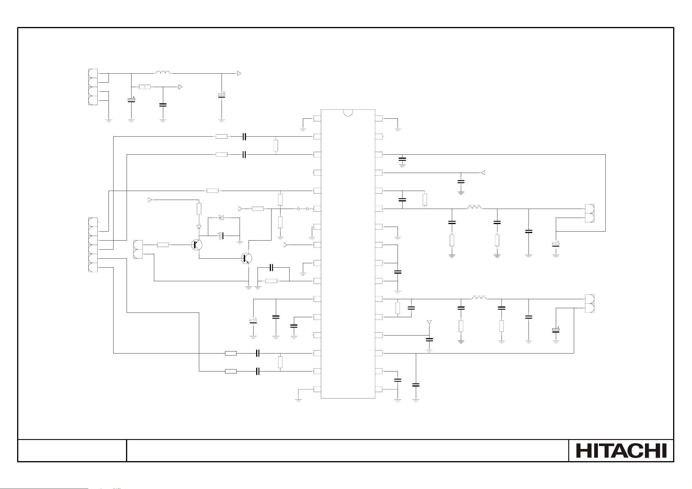
PL707
1
2
3
4
50V
470u
R22
10R
C127
L3
22u
C135
100n
50V
VPA
50V
470u
VP
C128
IC1
PL709
1
VSSD/HW1
VPA
BC848C
C123
470n
C124
470n
Q2
16V
16V
R10
47k
R24
30012677
25V
100n
C106
R9
39k
VPA
11k
S3
R11
1k
12k
2
IN1P
3
IN1N
4
DIAG
5
ENGAGE
S4
6
POWER_UP
7
CGND
8
VDDA
TDA8932
9
VSSA
10
OSCREF
R12
2.7k
R17
1N4001
R7
4k7
R8
4k7
D2
5V1
C130
220u
25V
IN1_R+
MUTE_3.3V
VPA
10k
6
5
4
3
2
1
PL704
1
2
R14
10k
Q1
BC858B
D1
HVP1
VDDP1
BOOT1
OUT1
VSSP1
STAB1
STAB2
VSSP2
32VSSD/HW4
31OSCIO
30
25V
100n
C105
29
C117
R18
10R
C118
470p
50V
28
1M
15n
R29
50V
C115
27
26
25
24
25V
100n
C104
23
100n
50V
47u
VP
L4
25V
100n
C116
63V
330n
C132
27R
R21
35V
1000u
C112
PL706
1
2
No. 0232
IN2_L+
R5
4k7
R6
4k7
50V
47u
C120
470n
16V
C121
470n
16V
C136
C107
R25
100n
11k
25V
C108
100n
25V
11
12
13
14
15
16
HVPREF
INREF
TEST
IN2N
IN2P
VSSD/HW2
OUT2
BOOT2
VDDP2
HVP2
DREF
VSSD/HW3
22
1M
R30
21
20
19
18
25V
100n
17
C114
C131
C101
15n
50V
100n
AMPLIFIER BOARD (18AMP06-3)
C102
25V
L5
47u
50V
470p
C113
VP
10R
R23
50V
100n
C103
27R
R20
100n
25V
C133
330n
63V
35V
1000u
C111
2
1
PL705
TFT TV Service Manual
54
Page 59
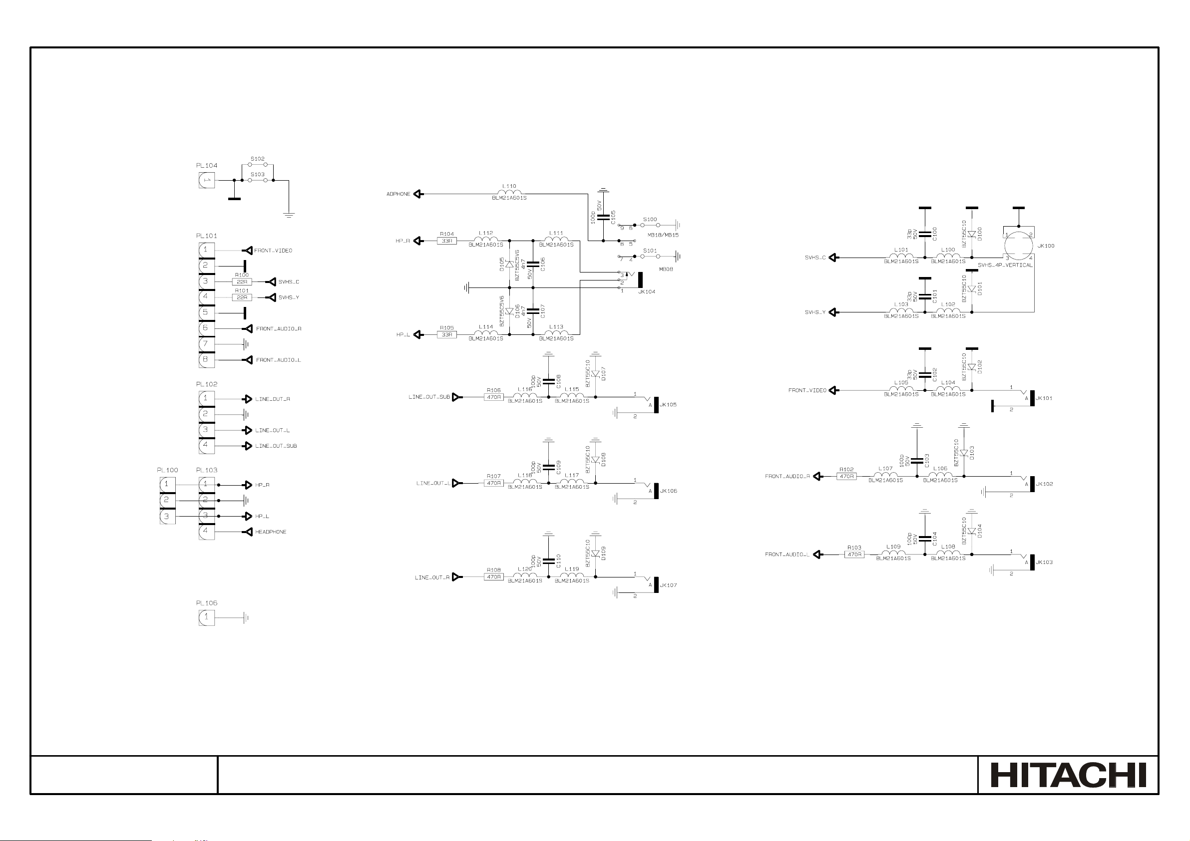
No. 0232
BAV BOARD (17BAV03-1)
TFT TV Service Manual
55
Page 60
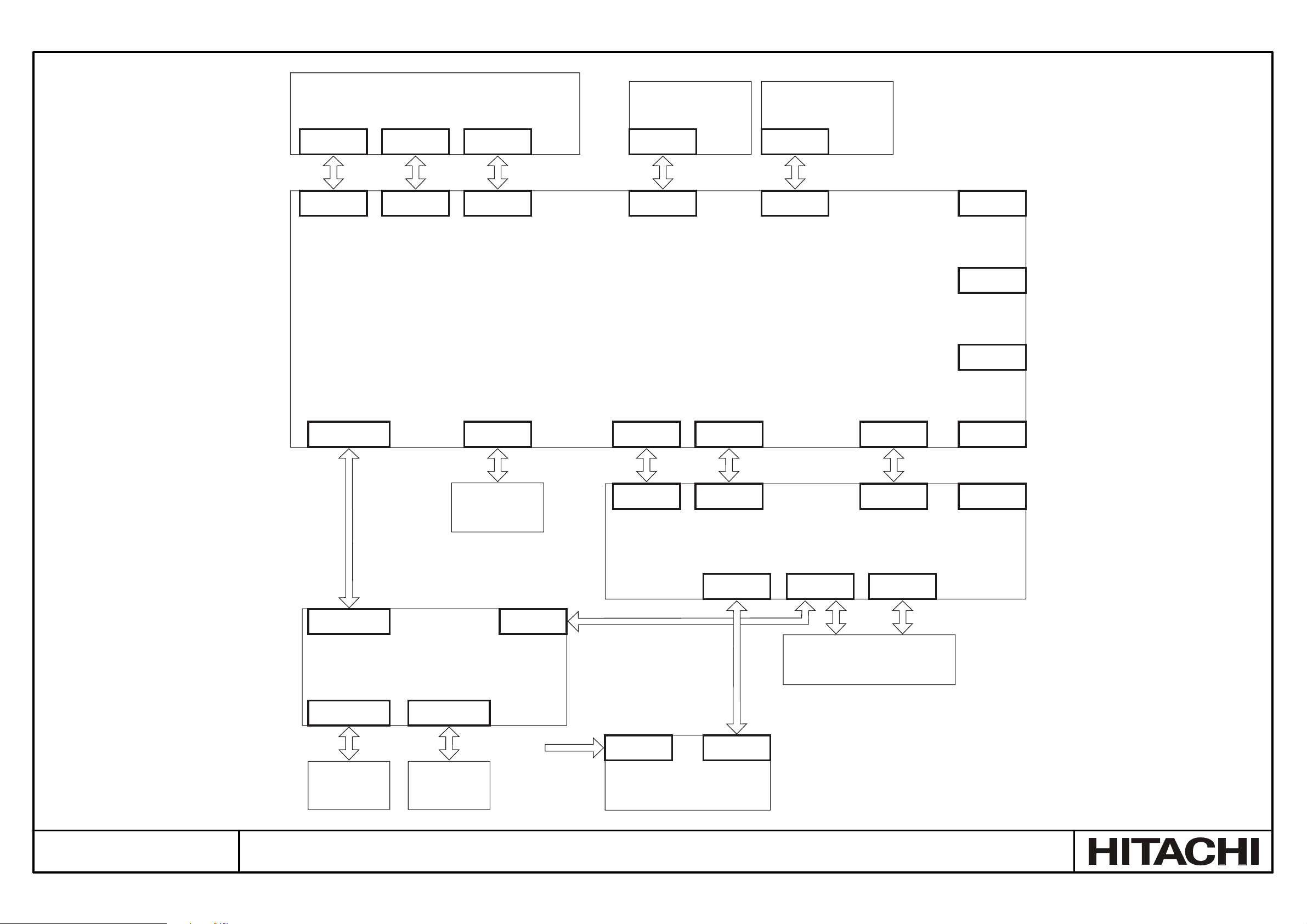
19.3. CONNECTOR DIAGRAM
FRONT AV
17FAV15
PL100 PL101
PL201 PL301 PL1002
PL102
KEYPAD
17TK46
PL1
PL606
MAIN BOARD
17MB15-E7
INFRARED
18LD02
PL1
PL600
PL206
PL104
PL308
PL103
PL709 PL707
PL705 PL706
LEFT
SPEAKER
RIGHT
SPEAKER
PL103
PANEL LVDS
AMPLIFIER
18AMP06
AC INPUT
PL900
PL805 PL806 PL803 PL807
PL100
17FL11-4
PL902
PSU
17PW15-9
PL800 PL801 PL802
PANEL INVERTER
CIRCUIT
PL3
PL901
PL1003
No. 0232
TFT TV Service Manual
CONNECTOR DIAGRAM
56
Page 61
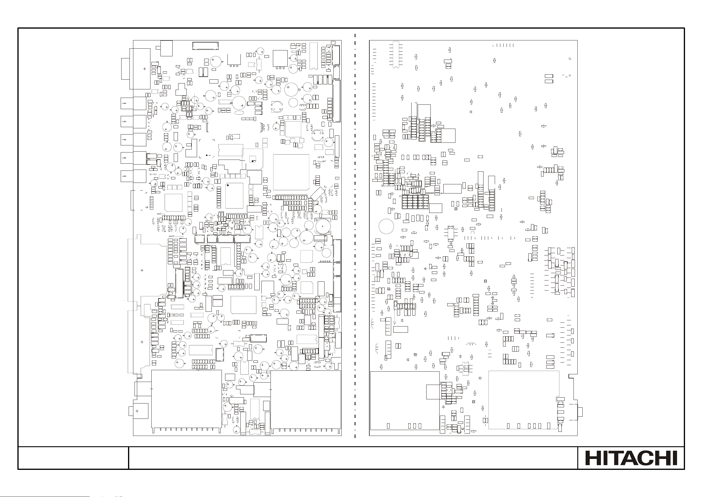
19.4. PCB LAYOUT
COMPONENT
(TOP) SIDE
PL2001
R418
X
4
A
R2027
R1071
C1166
C1024
L917
L928
C516
C410
R413
R414
R419
IC2001
R2026
R1070
IC208
C1169
L1019
Z1000
C1025
IC200
C1195
R2200
A
PL600
PL904
D902
D900
D901
PL900
L904
L903
L902
L901
L900
R900
R901
S903
S904
L931
L930
L920
L
9
0
5
IC903
C921
PL104
IC400
C423
S110
R2210
2
3
9
C426
0
S641
R422
S640
PL103
S109
1
S643
2
S642
C443
C444
C469
IC215
S645
S638
X
C1123
1
Z1003
S639
R250
R251
L910
L911
D911
K
C905
PL1004
L908
1
PL604
IC223
0
0
2
L1018
D914
PL901
C1152
S901
S900
C1201
B
L1002
C1200
R1126
S2013
R1124
S1009
Q1015
R1121
R1122
C1191
R1123
Q1016
L1032
C
D1007
C1045
C1198
R1022
R1031
R1025
C1037
D1003
C1202
C1042
R1038
PL604
PL901
S644
5
C1006
PL900
PL104
IC213
PL600
PL904
C903
S903
R901
R900
S904
L921
S448
L922
C923
C2405
C921
R6035
R6036
Q6008
R429
R433
R430
R432
R2239
C2407
R431
R2240
R2241
S600
R2218
S447
Q6009
R6037
L400
S646
S112
S113
S647
S111
C2211
C2406
R2212
S648
R2211
S444
C2207
0
4
C2220
X
C2221
C2254
R436
R435
C2222
C421
C2205
C2204
C2203
C415
C440
C2206
L408
L910
D904
S106
PL1004
S105
C905
R105
L908
S905
S911
R106
R904
R905
D602
C913
S902
S652
R107
D601
C1120
C1084
S651
R271
C1203
C1204
X1002
C1128
C1122
R1128
C1152
C1201
C1169
C1057
L1002
Z1000
S1010
L1032
C1006
Z1003
R1000
C947
C931
C912
C902
C900
L919
C530
C515
C521
C2250
C504
C507
C526
C510
C503
C532
C509
C506
C529
C523
C508
C531
C513
C511
C528
C512
C527
C522
R517
C1154
C451
S601
S633
C2048
R519
Q6011
C1147
C2200
C1013
R6042
C460
C520
C924
L1024
L402
C1121
C1119
X1000
R2223
R273
C2046
C1078
C449
R2224
Q204
C1007
Q205
R2225
L1026
C524
C927
C246
R266
C2202
C519
C525
C456
R6043
L409
L914
R1090
R2226
R1093
C1145
C1002
C2251
C448
R2227
R2228
R2229
R2230
L404
L916
C928
C1087
R1094
C1151
C1011
R505
R504
C500
L500
R518
C2252
C2253
R521
R6038
C452
R2217
C2210
C2209
C2208
C429
C427
S445
D101
S443
S446
C420
C422
R427
C467
0
R420
C409
C438
C439
C450
C457
S441
C414
C939
L406
C925
L407
S912
L915
C936
C911
Q206
R274
S635 R520
R269
R267
C2050
S634
R270
C245
R268
C2047
R104
C1079
C1081
C1086
R1078
C1112
C1177
C1114
C1113
C1117
C1125
C1130
C1118
C1137
C1144
C1140
L1022
L1023
C1028
C1153
C1163
C1170
R1110
R1105
R1109
R1107
C1035
R1028
C1036
TU1000
C945
L923
D912
R921
C943
C946
C918
C919
R524
C2404
L401
C431
C2215
C2403
C2402
C2214
C2401
C2400
C2213
C2212
S620
R2208
R2209
C1182
C1172
S621
R2215
R2216
C418
C2223
C2239
C2216
C2240
C2217
C2224
C2218
C2225
C2241
C2226
C2219
C2242
C430
C454
C455
C624
X600
IC218
C604
C294
C298
C940
R229
S326
L200
R1091
R1097
C283
C1132
C1124
L2011
C346
C347
C345
S345
PL1002
C1167
L1029
L1028
R1101
C1159
C1181
R1034
R1050
R1039
R1005
C1022
C1023
C1030
C1031
Z1001
C1027
C1026
R1117
C1188
C1186
R1116
D1006
L1031
C446
C447
C437
C435
C434
C425
R2238
R2237
R2236
R2235
R2221
C462
C463
R2222
R2220
R2219
R2234
R2233
R2232
R2231
C2231
C2227
C2232
C2228
C2233
C2229
C2230
C2234
C442
C465
C929
C938
C930
C941
C926
C937
C1080
C1150
R1096
R1092
R2202
C1134
C300
D1000
C1197
C1014
R1052
C1054
R1051
Q1005
C1055
S1003
R1048
C1052
R1049
R1010
R1114
R1009
C627
S302
C1162
R1012
R1115
C901
C909
C906
C908
PL607
C600
S624
C608
C613
R697
R6013
S610
R6030
S615
C622
C621
L609
C609
C612
R684
R686
R685
C623
R687
R693
C417
PL301
C268
C299
S325
R201
R200
R205
C280
C285
C331
C340
C343
C341
C344
C334
C335
C336
L312
PL207
L925
IC209
C1184
R1113
C1165
R1040
IC205
R1030
X1001
C1047
R1024
Z1002
D1002
R203
C1180
C1039
R6014
R6044
L308
C1183
R653
C625
C606
R654
C628
R656
C626
R657
R6031
C630
C633
S6313
R661
L603
R6017
C416
R416
Q400
PL308
R202
C297
C303
C259
X300
C317
C323
C319
C320
C318
C361
C348
C305
C349
R300
C306
C311
C312
C313
C948
PL1003
C1009
C2201
C1004
S1007
L1000
C1012
PL902
C914
PL205
L2012
C2087
C2088
L2014
C2082
C264
C2086
D203
D218
D211
D213
L1001
L2007
L2008
C2085
C2069
D2002
S323
C2068
C2073
C2080
C2079
S221
C1001
C2084
D226
D1004
PL200
JK300
JK301
JK302
C360
L317
S330
JK304
D225
C359
L316
S324
JK303
S331
C1000
PL2001
L213
L208
D220
C252
D1005
PL203
C255
L216
L218
L219
C257
R287
D204
D202
S220
D206
R286
D219
D209
R285
D214
D212
C250
R288
R289
R290
JK200
SOLDER
(BOTTOM) SIDE
D2502
D2501
C920
C2096
C2101
C2103
C2092
C607
C611
C620
PL206
R235
R304
C321
R306
C322
R305
R307
C350
C316
C2009
C2067
PL606
R240
C2005
R2009
R2008
C2007
R2006
C2006
C2008
L300
C2023
R2010
R2016
S2001
R2013
R2012
R2011
S2002
R2205
C2105
C2108
S2003
S2009
R2021
R2019
R2020
R2022
R2023
TU1001
R1001
C2095
C3009
C3006
C3004
C3001
C636
S803
R2053
C2070
S804
C2071
S805
C2075
C2076
IC2002
C2077
S800
L2013
C2065
C2064
C2054
C286
C267
C296
C2042
C2045
C2040
D2004
C2044
PL201
C351
R301
R2204
L2002
C249
L2019
C2024
C251
C254
C2022
C1010
R2206
S1000
C1008
C1015
C1003
C505
R523
C1194
C1192
S1008
IC206
C1087
IC204
R1037
C2200
S907
C1133
C1206
R1067
R1032
C1197
C915
R1095
C1199
R500 R501
C445
C928
C947
C931
B
R1036
R926
Q902
R507
L916
C1126
R1127
C1145
R1029
S608
S607
L919
R513
L2009
C1154
R516
C468
C1149
R1013
X1000
R924
R509
D
4
C1020
C912
0
R508
L1025
0
R522
C432
1
R
C1034
R925
S223
C502
C927
L914
C1028
Q903
R923
C900
C2046
C1036
R1042
R1043
R259
R258
R257
C290
R512
C518
R510
C517
IC1
C458
L915
R2028
C1078
IC213
R256
R255
D903
S649
C903
L926
C902
L927
L906
L918
L501
C501
R503
R511
IC401
IC224
C436
C412
0
0
X
C939
C459
C911
D904
C1085
R1011
R1008
C1029
C1021
C
Q1003
C1048
TU1000
R6018
Q6006
R248
S6300
R246
A
R6015
R277
S6312
R265
R6016
S637
S6310
S6311
Q6007
S650
R6019
R208
R209
D201
R210
PL200
S654
R212
R213
R214
R238
R331
D106
JK300
JK301
JK302
JK304
JK303
C2081
PL205
PL203
1
C2056
C2057
L2004
L2006
L2003
L2005
1
1
R2066
L206
L204
L210
L205
3 2
R2070
C2069
R2035
R2071
C2058
L203
L207
L209
L211
L212
L214
IC2012
R2068
C2059
R2025
R2024
C269
D224
JK200
1
R252
C258
R254
C278
R2065
R2038
D2022
D2021
R2064
C2078
D104
D102
R333
C365
C358
C2063
D2000
R275
1
S817
S816
S815
S814
S813
S812
S811
S810
C2066
D2101
S636
C356
C363
C364
R332
C357
D2102
D222
D2500
D2104
D2003
D2105
R2039
C2038
S205
R312
R313
D2020
IC2013
TP100
C293
C248
C253
C3008
C3007
L2016
R2069
IC211
C3005
R2063
R2067
D205
D2100
D207
R215
R218
R219
C289
C3004
R2099
IC2002
C2074
D208
D200
C2072
R253
R276
R211
C2088
C3002
C2060
L2015
C3003
C3000
D2103
D223
C266
C2049
S204
C2095
R2076
R2075
R2077
C2090
IC2003
R2062
C270
R249
C301
C284
D221
C277
R2203
L2018
S653
R217
C302
C2055
R2015
Q2
R2030
C2083
C2039
C352
D2001
Q208
R283
IC212
R216
C2098
C2097
R2098
R260
D210
R325
C3009
S802
R261
S310
L2017
R2051 R2052
S340
C1010
R284
R2073
C2094
R2085
R2086
C3006
C3001
C362
C2089
C2061
C251
C247
L2001
C2021
R281
R282
Q207
R2084
R2082
R2083
C2099
R2074
IC2006
R2078
R2079
IC3000 IC3001
R
6
Q
0
0
6
5
0
6
C636
S818
S819
S6315
R600
R2050
R6006
C2062
S801
Z
R2002
PL201
IC316
S312
IC317
S311
C2024
C254
C2022
C2107
C2106
C2104
C2093
R602
Q2299
R2306
C635
C2037
C2036
K
C2064
R2001
R
C2034
C2033
C2052
C2053
R606
IC315
S341
2
0
C2031
C2032
TU1001
C2051
C281
R6007
R225
R224
R223
R222
R221
R220
C2008
1
4
C2030
C2029
R279
R6046
R2305
R607
Q600
C272
R291
C2028
C2027
R280
IC2008
R6039
S614
R604
C634
R2042 R2046 R2047 R2049
R2040
R2041
C2067
Q2000
R2003
R1046
C271
C2020
PL902
17MB15E-7
L909
L913
IC214
D906
R2089
R2090
C2096
C2101
C2102
R2091
C2091
R2080
R2081
C2092
R6040
R692
S613
R610
R611
S604
Q602
Q603
Q604
Q605
S605
Q601
R6010
S606
R6011
R601
R2048
R2094
R2045
R2044
R2043
S807
R2097
S806
S809
D2023
D600
R237
R242
Q202
R1033
Q1004
R1045
Q200 Q203
Q2002 Q2003
Q2001
C282
R2007
C2005
C2007
C2006
S344
C2017
C2019
R292
C2016
C2018
C914
C916
R902
IC902
D905
C353
C920
S337
S336
IC318
C2103
R326
S307
S314
R2088
R2087
S308 S309
2
C2100
1
C620
R2095
Q2004
C2010
S2000
R102
Q100
S
1
S107
C611
R239
R2005"
C2026
S623
C405
C407
R424
R423
R244
C413
R103
R408
R404
0
8
R628
R624
R625
L600
L601
R688
R689
R690
R694
R695
R696
R698
R660
R655
K
Q6010
R603
IC2014
R6045
Q6012
S628
S629
R2096
PL308
PL206
C275
IC210
R226
R264
C304
C330
C332
C333
X300
C2004"
R2004"
L2000"
C317
C322 C321
S316
C316
C327
C328
PL207
1
C2009
2
IC2000
C948
PL1003
C2025
R2017
R2018
C1039
R1044
C1196
C2201
L1000
IC219
C605
R100
S
6
3
1
R101
6
C607
Q1
S808
PL606
R231
C276
R230
R241
R227
L201
L202
C262
R232
R293
C263
D216
S342
D217
D215
C261
Z
C350
S343
C2013
C2015
C2011
C2012
C2014
R1035
Q1002
C401
R401
S430
R315
R1026
C910
C909
S627
R316
C329
L925
C1180
R1112
R2201
C408
R405
S427
C1179
R903
S439
C404
R407
R317
C1012
R1103
C1049
C601
S438
C400
R400
C416
C1043
L907
C331
L311
C1009
R1041
C1041
R1027
C908
PL607
C402
R402
S431
C
C1183
C406
R403
B
R309
9
0
R1119
S2012
C942
IC900
C904
R919
R920
L932
C901
C906
S6320
IC217
C403
C2235
C2236
R406
C2237
C2238
S425
C466
R626
R627
E
E
Q400
S200
R207
C292
R2031
R2032
L313
R310
R311
1
C337
C338
D1001
C339
C1185
2
L1027
IC209
C1165
R1118
Q1014
C1189
Q1013
R1120
C1038
X1001
C1040
R1023
Z1002
IC904
R916
R917
R912
S6319
X
R204
S1005
S6314
IC220
L2010
R914
D910
R6041
R318
E
S1006
C1056
C1187
R
R907
S6318
R691
X600
S6322
S6321
C417
PL301
3
R319
C944
R918
Q901
R412
R679
S412
R415
S414
R629 R639
R640
R632
C299
L314
S
3
2
0
C342
L1030
C1162
C1173
IC201
L1031
R648
L604
C291
C273
C288
S201
C279
C265
C287
C260
R206
C274
0
R1102
R922
R680
C631
C419
R417
1
R1129
C946
S6317
R681
R2300
R2301
R1100
C1181
010606
VER
IC901
C945
L924
L923
R913
C917
R911
R910
R908
Q900
D907
D908
D909
0
6
9
5
S622
IC622
R676
R682
E
IC221
C428
C424
S437
R426
S413
C615
R2303"
C610
IC623
S603
C298
C283
C1132
D
C1158
C164
C1175
C1171
R1111
R322
IC216
R321
PL1002
C1167
C1168
C1178
C1159
C1030
Z1001
L912
C918
C932
R909
C933
R915
C935
C919
C922
C934
LF
R525
R515
C514
C2404
C433
R502
R506
R2214
R514
R2213
R425
C411
S411
S426
Q2301
Q2300
R2304
R2302
C929
S602
IC218
C930
D913
C941
C940
C1080
IC207
R1069
Q1011
Q1007
Q1009
R1068
C1124
C1136
C1138
C1157
C1148
C1156
C2202
C1097
C1106
C1174
C1176
C1116
R1106
R1108
L1017
R1089
R1098
R1104
L1021
L1020
C1134
C300
R323
R1130
L315
S303
R2033
C295
C1151
R2029
C1193
R1125
C1005
L1003
C1011
C1014
C1172
C1205
E
No. 0232
TFT TV Service Manual
MAIN BOARD
57
Page 62

THE UPDATED PARTS LIST
FOR THIS MODEL IS
AVAILABLE ON ESTA
58
Page 63

Hitachi, Ltd. Tokyo, Japan
International Sales Division
THE HITACHI ATAGO BUILDING,
No. 15 –12 Nishi Shinbashi, 2 – Chome,
Minato – Ku, Tokyo 105-8430, Japan.
Tel: 03 35022111
HITACHI EUROPE LTD,
Whitebrook Park
Lower Cookham Road
Maidenhead
Berkshire
SL6 8YA
UNITED KINGDOM
Tel: 01628 643000
Fax: 01628 643400
Email: consumer [email protected]
HITACHI EUROPE GmbH
Munich Office
Dornacher Strasse 3
D-85622 Feldkirchen bei München
GERMANY
Tel: +49-8 9-991 80-0
Fax: +49-89-991 80-224
Hotline: +49-180-551 25 51 (12ct/min)
Email: [email protected]
HITACHI EUROPE srl
Via Tommaso Gulli N.39, 20147
Milano, Italia
ITALY
Tel: +39 02 487861
Tel: +39 02 38073415 Servizio Clienti
Fax: +39 02 48786381/2
Email: [email protected]
HITACHI EUROPE S.A.
364 Kifissias Ave. & 1, Delfon Str.
152 33 Chalandri
Athens
GREECE
Tel: 1-6837200
Fax: 1-6835964
Email: [email protected]
HITACHI EUROPE S.A.
Gran Via Carlos III, 86, planta 5
Edificios Trade - Torre Este
08028 Barcelona
SPAIN
Tel: +34 93 409 2550
Fax: +34 93 491 3513
Email: [email protected]
HITACHI Europe AB
Box 77 S-164 94 Kista
SWEDEN
Tel: +46 (0) 8 562 711 00
Fax: +46 (0) 8 562 711 13
Email: [email protected]
HITACHI EUROPE S.A.S
Lyon Office
B.P. 45, 69671 BRON CEDEX
FRANCE
Tel: +33 04 72 14 29 70
Fax: +33 04 72 14 29 99
Email: [email protected]
HITACH EUROPE AB
Egebækgård
Egebækvej 98
DK-2850 Nærum
DENMARK
Tel: +45 43 43 6050
Fax: +45 43 60 51
Email: [email protected]
Hitachi Europe Ltd
Bergensesteenweg 421
1600 Sint- Pieters-Leeuw
BELGIUM
Tel: +32 2 363 99 01
Fax: +32 2 363 99 00
Email: [email protected]
www.hitachidigitalmedia.com
HITACHI EUROPE LTD (Norway) AB
STRANDVEIEN 18
1366 Lysaker
NORWAY
Tel: 67 5190 30
Fax: 67 5190 32
Email: [email protected]
HITACHI EUROPE AB
Neopoli / Niemenkatu 73
FIN-15140 Lahti
FINLAND
Tel : +358 3 8858 271
Fax: +358 3 8858 272
Email: [email protected]
HITACHI EUROPE LTD
Na Sychrove 975/8
101 27 Pr aha 10 – Bohdalec
CZECH REPUBLIC
Tel: +420 267 212 383
Fax: +420 267 212 385
Email: [email protected]
 Loading...