HIT 2SK2922 Datasheet

2SK2922
Silicon N Channel MOS FET
UHF Power Amplifier
ADE-208-675(Z)
1st. Edition
Aug. 1998
Features
• High power output, High gain, High efficiency
PG = 8.0dB, Pout = 31dBm, ηD = 57 %min. (f = 836.5MHz)
• Compact package capable of surface mounting
Outline
1
2
3
4
UPAK
1. Gate
2. Source
3. Drain
4. Source
This Device is sensitive to Electro Static Discharge.
An Adequate handling procedure is requested.

2SK2922
2
Absolute Maximum Ratings (Ta = 25°C)
Item Symbol Ratings Unit
Drain to source voltage V
DSS
10 V
Gate to source voltage V
GSS
±6V
Drain current I
D
0.7 A
Drain peak current I
D(pulse)
Note1
1.4 A
Channel dissipation Pch
Note2
3W
Channel temperature Tch 150 °C
Storage temperature Tstg –45 to +150 °C
Note: 1. PW ≤ 10ms, duty cycle ≤ 50 %
2. Value at Tc = 25°C
Electrical Characteristics (Ta = 25°C)
Item Symbol Min Typ Max Unit Test Conditions
Zero gate voltage drain current I
DSS
— — 100 µAVDS = 10 V, VGS = 0
Gate to source leak current I
GSS
——±5.0 µAVGS = ±6V, VDS = 0
Gate to source cutoff voltage V
GS(off)
0.4 — 1.2 V ID = 3mA, VDS = 5V
Input capacitance Ciss — 27 — pF VGS = 2V, VDS = 0, f = 1MHz
Output capacitance Coss — 13 — pF VDS = 5, VGS = 0, f = 1MHz
Output Power Pout 31 — — dBm VDS = 4.7V, f =836.5Mhz
Pin = 23dBm
Drain Rational ηD 57——%V
DS
= 4.7V, f =836.5Mhz
Pin = 23dBm
Note: 1. Marking is “HX”.

2SK2922
3
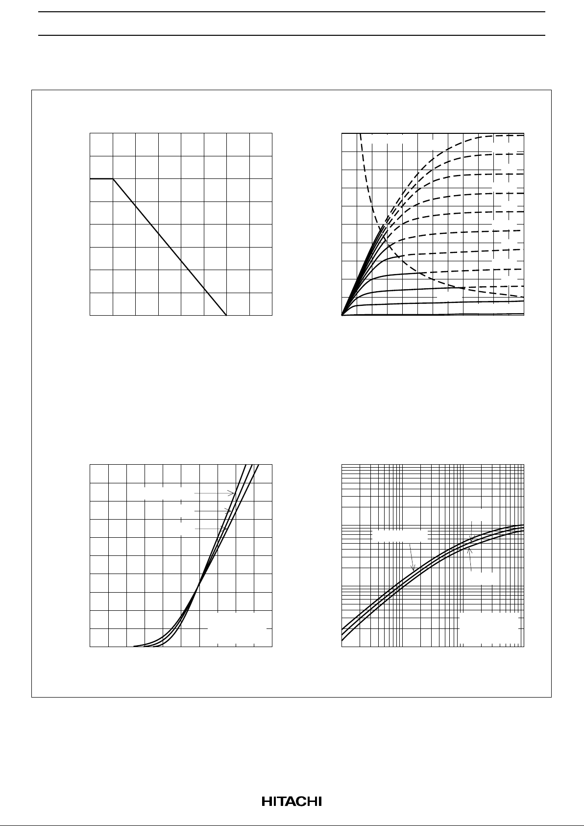
Main Characteristics
0
50 100 150 200
4
3
2
1
1.0
0.8
0.6
0.4
0.2
0
0.5 1.0 1.5 2.0 2.5
5
4
3
2
1
0
1
2345
6
5 V
6 V
Tc = –25°C
25°C
75°C
0.001
1
0.3
0.03
0.1
0.003 0.01 0.3 0.1 0.3 1
0.01
Channel Power Dissipation Pch (W)
Case Temperature Tc (°C)
Maximum Channel Power
Dissipation Curve
Drain to Source Voltage V (V)
DS
Drain Current I (A)
D
Typical Output Characteristics
Pulse Test
V = 5 V
Pulse Test
DS
Gate to Source Voltage V (V)
GS
Drain Current I (A)
D
Typical Transfer Characteristics
Drain Current I (A)
D
Forward Transfer Admittance |y | (S)
fs
Forward Transfer Admittance
vs. Drain Current
5.5 V
V = 1 V
GS
4.5 V
4 V
3.5 V
3 V
2.5 V
2 V
1.5 V
V = 5 V
Pulse Test
DS
Tc = –25°C
25°C
75°C
3
10
 Loading...