

HIT 2SB791(K) Datasheet
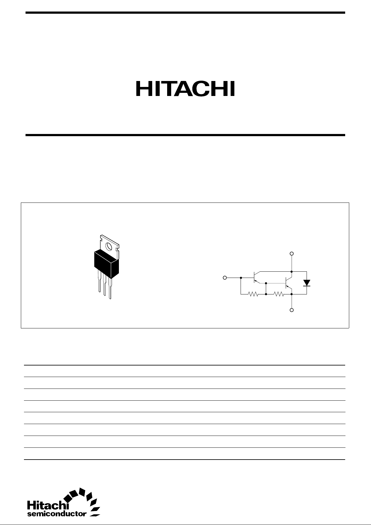
2SB791(K)
Silicon PNP Epitaxial
Application
Medium speed and power switching complementary pair with 2SD970(K)
Outline
TO-220AB
2 kΩ
(Typ)
200 Ω
(Typ)
1
2
3
1. Base
2. Collector
(Flange)
3. Emitter
1
2
3
Absolute Maximum Ratings (Ta = 25°C)
Item Symbol Rating Unit
Collector to base voltage V
CBO
–120 V
Collector to emitter voltage V
CEO
–120 V
Emitter to base voltage V
EBO
–7 V
Collector current I
C
–8 A
Collector peak current I
C(peak)
–12 A
Collector power dissipation PC*
1
40 W
Junction temperature Tj 150 °C
Storage temperature Tstg –55 to +150 °C
Note: 1. Value at TC = 25°C
2SB791(K)
2
Electrical Characteristics (Ta = 25°C)
Item Symbol Min Typ Max Unit Test conditions
Collector to emitter breakdown
voltage
V
(BR)CEO
–120 — — V IC = –25 mA, RBE = ∞
Emitter to base breakdown
voltage
V
(BR)EBO
–7 — — V IE = –50 mA, IC = 0
Collector cutoff current I
CBO
— — –100 µAV
CB
= –120 V, IE = 0
I
CEO
— — –10 µAV
CE
= –100 V, RBE = ∞
DC current transfer ratio h
FE
1000 — 20000 VCE = –3 V, IC = –4 A*
1
Collector to emitter saturation V
CE(sat)(1)
— — –1.5 V IC = –4 A, IB = –8 mA*
1
voltage V
CE(sat)(2)
— — –3.0 V IC = –8 A, IB = –80 mA*
1
Base to emitter saturation V
BE(sat)(1)
— — –2.0 V IC = –4 A, IB = –8 mA*
1
voltage V
BE(sat)(2)
— — –3.5 V IC = –8 A, IB = –80 mA*
1
Turn on time t
on
— 0.5 — µsI
C
= –4 A, IB1 = IB2 = –8 mA
Storage time t
stg
— 1.6 — µs
Fall time t
f
— 1.5 — µs
Note: 1. Pulse test
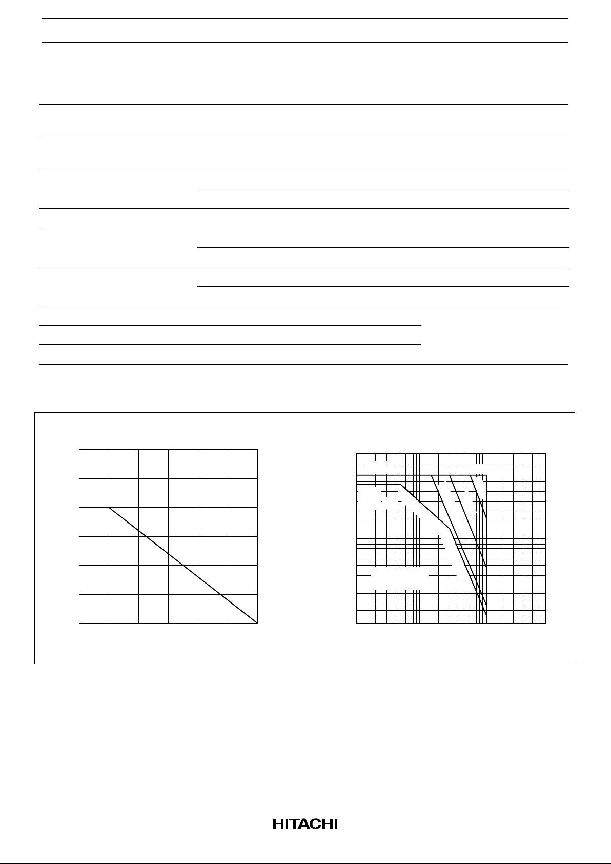
Maximum Collector Dissipation
Curve
60
40
20
0 50 100 150
Case temperature T
C
(°C)
Collector power dissipation P
C
(W)
Area of Safe Operation
–30
–10
–3
–1.0
–0.3
Collector current I
C
(A)
–0.1
–0.03
–1 –10 –100 –1,000–3 –30 –300
Collector to emitter voltage V
CE
(V)
Ta = 25°C
1 Shot Pulse
i
C(peak)
1 µs
I
Cmax
(Continuous)
DC Operation
(T
C
= 25°C)
PW = 10 ms
1 ms
10 µs
 Loading...