

Page 1
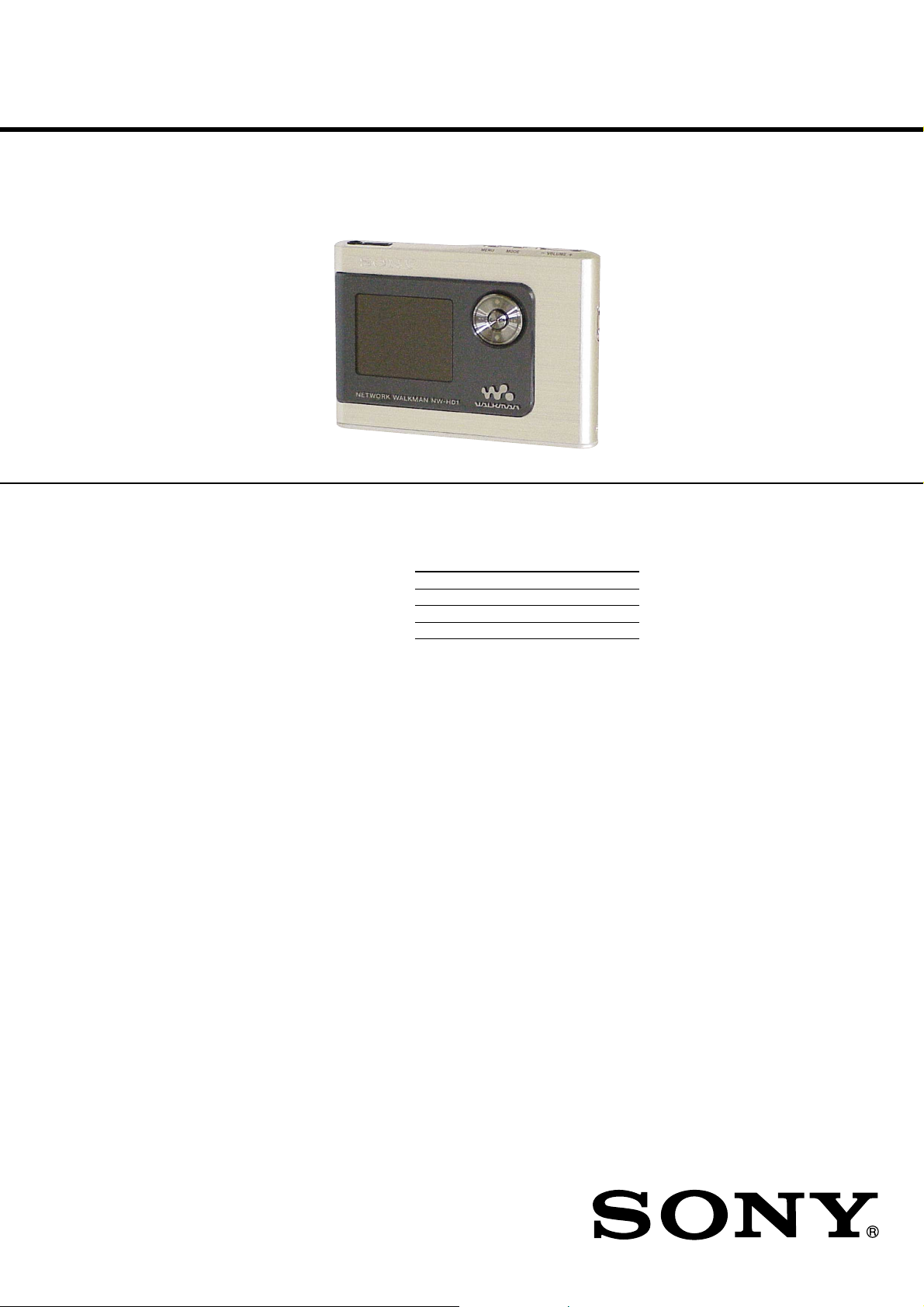
NW-HD1
SERVICE MANUAL
Ver 1.1 2004.09
• SonicStage and SonicStage logo are trademarks or registered
trademarks of Sony Corporation.
• OpenMG, ATRAC3, ATRAC3plus and their logos are trademarks
of Sony Corporation.
• Microsoft, Windows, Windows NT and Windows Media are
trademarks or registered trademarks of Microsoft Corporation in
the United States and/or other countries.
• IBM and PC/AT are re gistered trademarks of International Business
Machines Corporation.
• Macintosh is a trademark of Apple Computer, Inc. in the United
States and/or other countries.
• Pentium is a trademark or a registered trademark of Intel
Corporation.
• Adobe and Adobe Reader are trademarks or registered trademarks
of Adobe Systems Incorporated in the United States and/or other
countries.
• US and foreign patents licensed from Dolby Laboratories.
• All other trademarks and registered trademarks are trademarks or
registered trademarks of their respective holders.
• In this manual, TM and ® marks are not specifi ed.
Maximum recordable number of track
(Approx.)*
ATRAC3 ATRAC3plus
5,000 (132 kbps) 2,500 (256 kbps)
6,000 (105 kbps) 10,000 (64 kbps)
10,000 (66 kbps) 13,000 (48 kbps)
* When transferring four-minute tracks
Sampling frequency
44.1 kHz
Audio compression technology
Adaptive Transform Acoustic Coding3 (ATRAC3),
Adaptive Transform Acoustic Coding3plus
(ATRAC3plus)
Frequency response
20 to 20,000 Hz
(single signal measurement during playback)
Output
i
(headphones)/LINE OUT* :
Stereo minijack/194 mV
* The jack is used for both headphones and LINE
OUT.
Operating temperature
5 to 35ºC (41 to 95ºF)
Power source
DC IN 6 V (from built-in rechargeable battery)
Battery life (continuous playback)
ATRAC3plus format (48 kbps): Approx. 30 hours
Canadian Model
SPECIFICATIONS
Dimension
Not including projecting parts:
89.0 × 62.1 × 13.8 (the thinnest part 12.6) mm
(3 5/8 × 2 1/2 × 9/16 (the thinnest part 1/2)
inches) (w/h/d)
Including projecting parts:
89.2 × 63.4 × 14.3 mm
(3 5/8 × 2 1/2 × 19/32 inches) (w/h/d)
Mass
Approx. 110 g (3.9 oz)
US and foreign patents licensed from Dolby
Laboratories.
Supplied accessories
• Headphones (1)
• USB cradle (1)
• Dedicated USB cable (1)
• AC power adaptor (1)
(For the supplied USB cradle)
• Carrying pouch (1)
• CD-ROM (1) *
(SonicStage, PDF of Operating Instructions)
• Quick Start Guide (1)
* Do not play this CD-ROM on an audio CD player.
Design and speci cations are subject to change
without notice.
US Model
AEP Model
UK Model
9-879-079-02
2004I05-1
© 2004.09
PORTABLE HARD DISK AUDIO PLAYER
Sony Corporation
Personal Audio Company
Published by Sony Engineering Corporation
Page 2

NW-HD1
Ver 1.1
Notes on the AC power adaptor
Use only the AC power adaptor and USB
cradle supplied with the player. Do not use
any other AC power adaptor since this may
cause the player to malfunction.
The player is not disconnected from the
AC power source (mains) as long as it is
connected to the wall outlet, even if the
player itself has been turned off.
If you are not going to use the player for a
long time, be sure to disconnect the power
supply. To remove the AC power adaptor
from the wall outlet, grasp the adaptor plug
itself; never pull the cord.
Notes on chip component replacement
• Never reuse a disconnected chip component.
• Notice that the minus side of a tantalum capacitor may be
damaged by heat.
Flexible Circuit Board Repairing
• Keep the temperature of the soldering iron around 270 ˚C
during repairing.
• Do not touch the soldering iron on the same conductor of the
circuit board (within 3 times).
• Be careful not to apply force on the conductor when soldering
or unsoldering.
TABLE OF CONTENTS
1. SERVICING NOTES ............................................... 3
2. GENERAL ................................................................... 4
3. DISASSEMBLY
3-1. Disassembly Flow ........................................................... 5
3-2. Cabinet (Upper) Sub Assy............................................... 5
3-3. Cabinet (Lower) Assy...................................................... 6
3-4. Battery Block Sub Assy................................................... 6
3-5. MAIN Board.................................................................... 7
3-6. LCD Block Sub Assy ...................................................... 7
3-7. HDD Unit, HDD Board ................................................... 8
4. TEST MODE.............................................................. 9
5. DIAGRAMS
5-1. Block Diagram –MAIN Section (1/2) – .......................... 16
5-2. Block Diagram –MAIN Section (2/2) – .......................... 17
5-3. Block Diagram –KEY/POWER SUPPLY Section –....... 18
5-4. Printed Wiring Board
– MAIN Section (Component Side) – ............................. 20
5-5. Printed Wiring Board
– MAIN Section (Conductor Side) –............................... 21
5-6. Schematic Diagram –MAIN Section (1/7) – ................... 22
5-7. Schematic Diagram –MAIN Section (2/7) – ................... 23
5-8. Schematic Diagram –MAIN Section (3/7) – ................... 24
5-9. Schematic Diagram –MAIN Section (4/7) – ................... 25
5-10. Schematic Diagram –MAIN Section (5/7) –................... 26
5-11. Schematic Diagram –MAIN Section (6/7) –................... 27
5-12. Schematic Diagram –MAIN Section (7/7) –................... 28
5-13. Printed Wiring Board – HDD Section – ......................... 29
5-14. Schematic Diagram – HDD Section –............................ 29
SAFETY-RELATED COMPONENT WARNING!!
COMPONENTS IDENTIFIED BY MARK 0 OR DOTTED LINE
WITH MARK 0 ON THE SCHEMATIC DIAGRAMS AND IN
THE PARTS LIST ARE CRITICAL TO SAFE OPERATION.
REPLACE THESE COMPONENTS WITH SONY PARTS WHOSE
PART NUMBERS APPEAR AS SHOWN IN THIS MANUAL OR
IN SUPPLEMENTS PUBLISHED BY SONY.
6. EXPLODED VIEW ................................................... 42
7. ELECTRICAL PARTS LIST................................ 43
ATTENTION AU COMPOSANT AYANT RAPPORT
À LA SÉCURITÉ!
LES COMPOSANTS IDENTIFIÉS P AR UNE MARQ UE 0 SUR
LES DIAGRAMMES SCHÉMATIQUES ET LA LISTE DES
PIÈCES SONT CRITIQUES POUR LA SÉCURITÉ DE
FONCTIONNEMENT. NE REMPLACER CES COM- POSANTS
QUE PAR DES PIÈCES SONY DONT LES NUMÉROS SONT
DONNÉS DANS CE MANUEL OU D ANS LES SUPPLÉMENTS
PUBLIÉS PAR SONY.
2
Page 3

SECTION 1
SERVICING NOTES
NW-HD1
UNLEADED SOLDER
Boards requiring use of unleaded solder are printed with the leadfree mark (LF) indicating the solder contains no lead.
(Caution: Some printed circuit boards may not come printed with
the lead free mark due to their particular size)
: LEAD FREE MARK
Unleaded solder has the following characteristics.
• Unleaded solder melts at a temperature about 40 ˚C higher
than ordinary solder.
Ordinary soldering irons can be used but the iron tip has to be
applied to the solder joint for a slightly longer time.
Soldering irons using a temperature regulator should be set to
about 350 ˚C.
Caution: The printed pattern (copper foil) may peel away if
the heated tip is applied for too long, so be careful!
• Strong viscosity
Unleaded solder is more viscou-s (sticky, less prone to flow)
than ordinary solder so use caution not to let solder bridges
occur such as on IC pins, etc.
• Usable with ordinary solder
It is best to use only unleaded solder but unleaded solder may
also be added to ordinary solder.
• Replacement of CXR704060-201GA (IC1003),
MBM29SL800BE-90PBT (IC1101), S1R72003BOOA100
(IC2001), CXR710160-211GH (IC3001), CXD1616GH
(IC7001) and EDL1216CASA-10L-E (IC7002) used in this
set requires a special tool.
System requirements
Computer
Operating System
Display
Others
Notes
•
SonicStage is not supported by the following environments:
– Operating systems other than those the indicated above
– Personally constructed PCs or operating systems
– An environment that is an upgrade of the original manufacturer-installed operating system
– Multi-boot environment
– Multi-monitor environment
– Macintosh
•
We do not guarantee trouble-free operation on all computers that satisfy the system requirement.
•
The NTFS format of Windows XP/Windows 2000 Professional can be used only with the standard (factory)
settings.
•
For Windows 2000 Professional users, install Service Pack 3 or later version before using the software.
•
We do not guarantee trouble-free operation of the system suspend, sleep, or hibernation function on the
computers.
IBM PC/AT or Compatible
• CPU: Pentium II 400 MHz or higher (Pentium III 450 MHz or higher is
recommended.)
• Hard disk drive space: 200 MB or more (1.5 GB or more is recommended.) (The
amount of space will vary according to the Windows version and the number of
music les stored on the hard disk.)
• RAM: 64 MB or more (128 MB or more is recommended.)
Others • CD drive (capable of digital playback by WDM)
• Sound Board
• USB port (Hi-Speed USB is supported.)
Factory installed:
Windows XP Media Center Edition 2004/Windows XP Media Center Edition/
Windows XP Professional/Windows XP Home Edition/Windows 2000 Professional/
Windows Millennium Edition/Windows 98 Second Edition
High Color (16 bit) or higher, 800 600 dots or better (1024 × 768 dots or better is
recommended.)
• Internet access: for Web registration, EMD services and CDDB
• Windows Media Player (version 7.0 or higher) installed for playing WMA les
3
Page 4
NW-HD1
SECTION 2
GENERAL
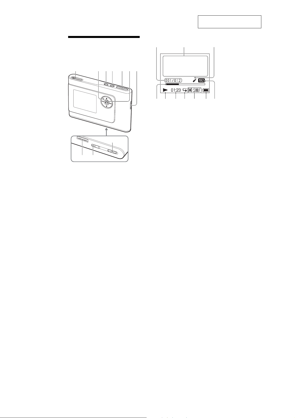
Guide to Parts and
Controls
Player
1234567
q;
8
9
1 i
(headphones)/LINE OUT jack
2 M, m, ., >
3
MENU button
4
MODE button
5
VOLUME +*/– buttons
6 Nx
(play/stop) button
7
Hole for hand strap**
8
USB cradle connector
9
BUILT-IN BATTERY switch
q;
HOLD switch
* This button has a tactile dot.
** You can attach your own hand strap.
buttons
This section is extracted from
instruction manual.
Player display
qa qs
qf qg qh qj qk w;ql
qa
Track number indicator
qs
Character information display
qd
Bookmark indicator
qf
Playback progress bar
qg
Playback indicator
qh
Playing time
qj
Repeat indicator
qk
Play mode indicator
Sound indicator
ql
Battery indicator
w;
Bit rate
qd
About the serial number
The serial number provided for this player is
required for the customer registration. The
number is on a label on the rear of the player.
4
Page 5
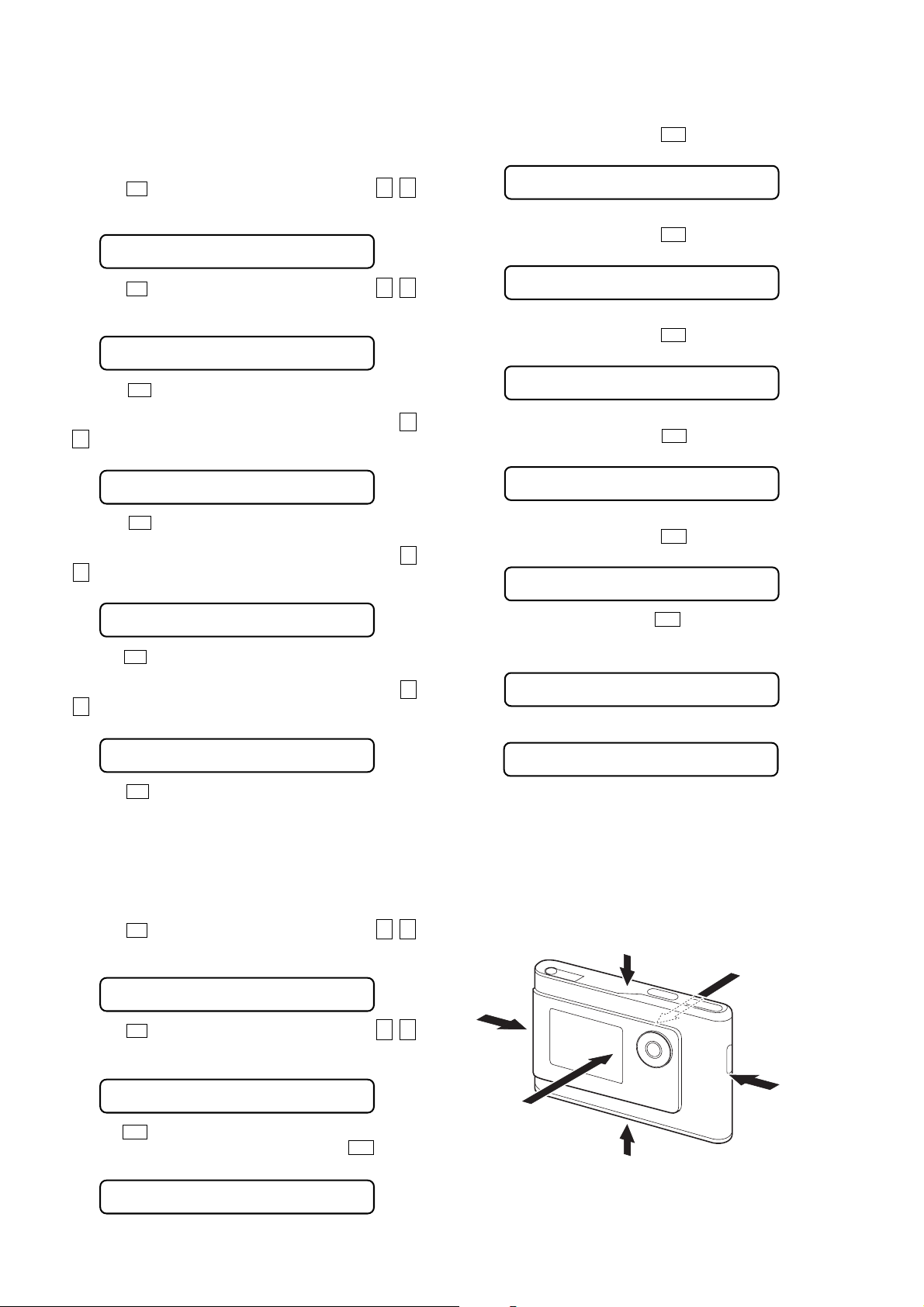
• This set can be disassembled in the order shown below.
3-1. DISASSEMBLY FLOW
SET
3-2. CABINET (UPPER) SUB ASSY
(Page 5)
3-3. CABINET (LOWER) ASSY
(Page 6)
3-4. BATTERY BLOCK SUB ASSY
(Page 6)
3-5. MAIN BOARD
(Page 7)
NW-HD1
SECTION 3
DISASSEMBLY
3-6. LCD BLOCK SUB ASSY
(Page 7)
Note: Follow the disassembly procedure in the numerical order given.
3-7. HDD UNIT, HDD BOARD
3-2. CABINET (UPPER) SUB ASSY
6
cabinet (upper) sub assy
3
(Page 8)
2
screw (M1.4)
5
flexible board
(CN5002)
1
screw (M1.4)
4
escutcheon (cradle)
5
Page 6
NW-HD1
)
3-3. CABINET (LOWER) ASSY
Note :When install the cabinet (lower) assy,
adjust the position of two switches (S5009, S9501)
and knob (batt, hold).
S9501
S5009
1
Remove the cabinet (lower)
assy in the direction of arrow.
knob (hold)
knob (batt)
3-4. BATTERY BLOCK SUB ASSY
2
toothed lock screw (M1.4)
3
battery block sub assy
1
connector (CN9501
6
Page 7
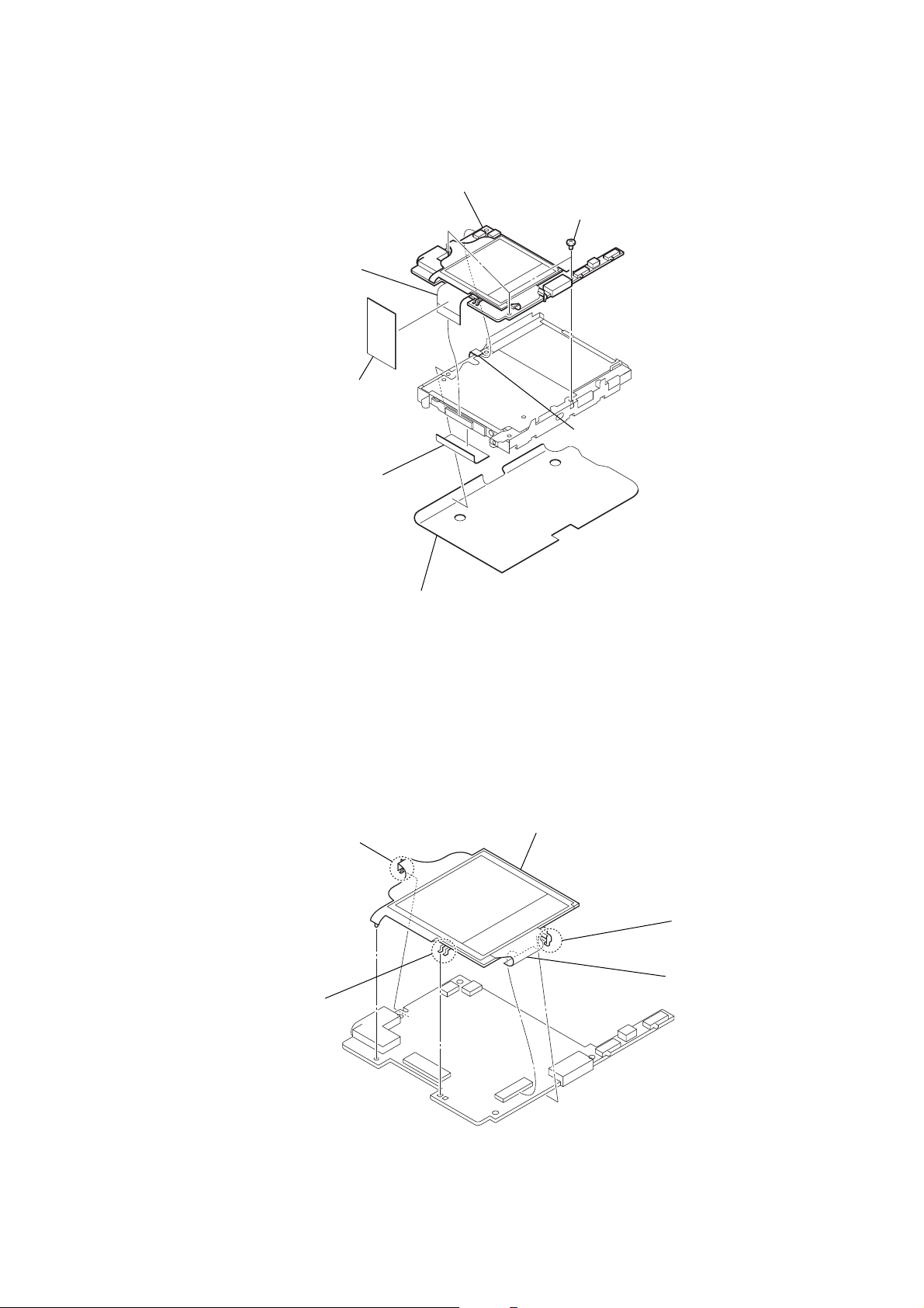
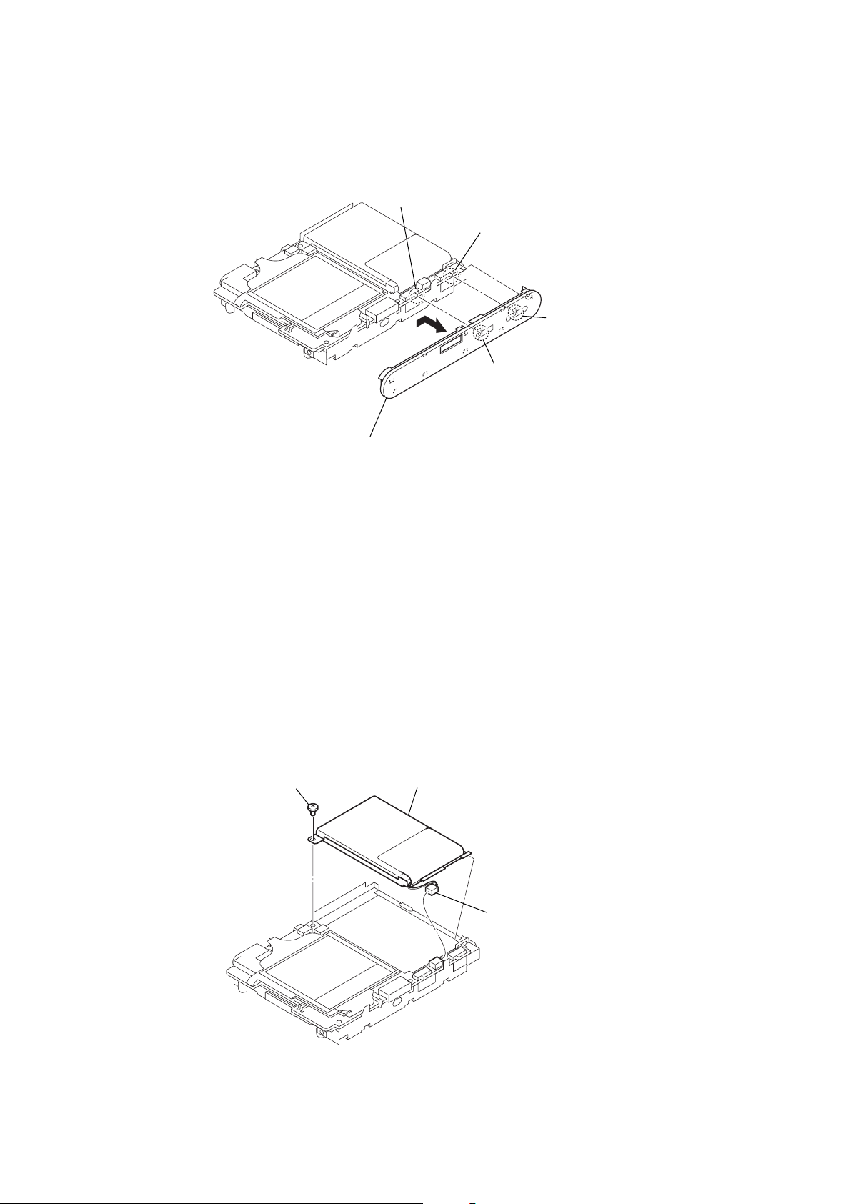
3-5. MAIN BOARD
3
sheet (insulating HDD flexible)
4
flexible board
(CN100)
2
7
sheet
(SHIELD HDD)
MAIN board
6
three toothed screws (M1.4)
5
flexible board
(CN5003)
NW-HD1
3-6. LCD BLOCK SUB ASSY
3
1
Remove two solders.
claw
1
sheet (damper)
4
LCD block sub assy
2
claw
5
flexible board
(CN5001)
7
Page 8
NW-HD1
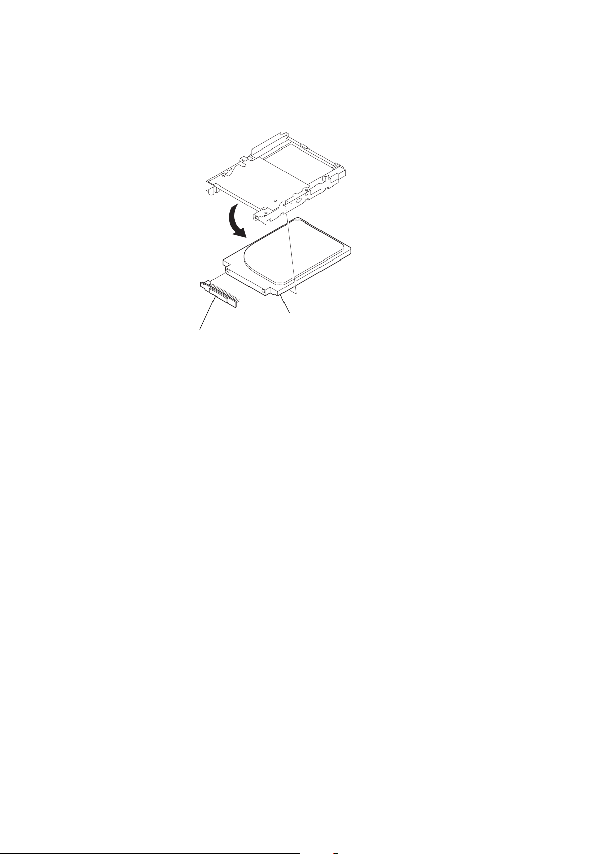
3-7. HDD UNIT, HDD BOARD
1
Remove the HDD unit in the direction of arrow.
2
HDD board
Note : Extraction and insertion of a HDD board is
performed perpendicularly.
8
Page 9
SECTION 4
TEST MODE
NW-HD1
Ver 1.1
1. OUTLINE
For the LCD display, the LCD on the main unit is shown, but the
contents of LCD display on the remote commander are same.
Operation in the test mode is performed with the main unit. A key
having no particular description in the text, indicates a main unit key.
Power supply voltage : 3.65 to 3.75 V
Volume : 24
SOUND EQ : OFF
AVLS : OFF
[HOLD] switch : OFF
Set states : horizontal states
2. SETTING THE TEST MODE
1. Supply power to the set.
2. Switch-on the [HOLD] switch on the main unit.
3. Operate as follows.
• When use only main unit
While pressing the [MODE] key on the main unit, press the key on
the main unit as following order.
> → > → . → . → > → . → > → .
→ M → m
• When use the main unit and remote commander
While pressing the [MODE] key on the main unit, press the key on
the remote commander as following order.
> → > → . → . → > → . → > → .
→ + → –
4. Switch-off the [HOLD] switch on the main unit and enter the
test mode.
5. OPERATION OF THE TEST MODE
5-1. Power
5-1-1. Power supply voltage check
This mode is used in case power supply voltage in the state where
all power supply lines (1.2 V/1.5 V/1.8 V/2.0 V/2.4 V/3.3 V/VSTBY/
VDC) are starting is checked.
Checking method:
1. Enter the test mode.
2. Press the , key to display major item, and press the M m
key to select the “POWER”.
LCD display
POWER
3. Press the , key to display minor item, and press the M m
key to select the “V CHK”.
LCD display
V CHK
4. Press the Bx ke y, “START” is displayed and all power supply
lines are started.
LCD display
START
5. Press the [MODE] key, “HD OFF/ON” is displayed. Each time
[MODE] key is pressed, hard disk drive power supply ON/OFF
switch is performed.
LCD display
HD OFF/ON
3. RELEASING THE TEST MODE
Press the [SET UP] key on the main unit or x key on the remote
commander for 1.5 seconds or more, turn off the power and release
the test mode.
4. CONFIGURATION OF THE TEST MODE
Flow of the test mode:
F/W version display
,
,
Bx
key
Start
Automatic
Finish
Result
key
Major item
key
Minor item
or
key
<
key
<
[SET UP]
Major item switching: key
Minor item switching: key
key
M m
M m
6. Press the [SET UP] key, return to minor item selection screen.
5-1-2. Consumption current (read state) check
This mode is used in case consumption current (read state) in the
state where the hard disk drive has booted is checked.
Checking method:
1. Enter the test mode.
2. Press the
key to select the “POWER”.
, key to display major item, and press the M m
LCD display
POWER
3. Press the , key to display minor item, and press the M m
key to select the “A RD”.
LCD display
A RD
4. Press the Bx key, “READY?” is displayed. In this state, Each
time [MODE] key is pressed, EL back light ON/OFF switch is
performed.
LCD display
READY?
9
Page 10
NW-HD1
Ver 1.1
5. Press the Bx key, “READ” is displayed and h ard disk drive
becomes read state.
After 10 seconds, “FIN” is displayed automatically and read
state is completed.
LCD display
READ
r
FIN
6. Press the [SET UP] key, return to minor item selection screen.
5-1-3. Consumption current (write state) check
This mode is used in case consumption current (write state) in the
state where the hard disk drive has booted is checked.
Checking method:
1. Enter the test mode.
2. Press the , key to display major item, and press the M m
key to select the “POWER”.
LCD display
POWER
3. Press the , key to display minor item, and press the M m
key to select the “A WR”.
LCD display
A WR
4. Press the Bx key, “READY?” is displayed. In this state, Each
time [MODE] key is pressed, EL back light ON/OFF switch is
performed.
LCD display
READY?
5. Press the
becomes write state.
After 10 seconds, “FIN” is displayed automatically and write
state is completed.
Bx key, “WRITE” is displayed and hard disk drive
LCD display
WRITE
r
FIN
6. Press the [SET UP] key, return to minor item selection screen.
5-2. Audio
The VOLUME + ke y on the main unit or [PLAY MODE] on the remote
commander performs switch of HP/LINE.
While playing the audio track, it's in a repeat state. If Bx key is
pressed, it’s stopped.
Setting method of the audio test mode:
1. The data for audio test mode is copied to hard disk drive.
2. Enter the test mode.
3. Press the , key to display major item, and press the M m
key to select the “AUDIO”.
LCD display
AUDIO
4. Press the
key to select the “TESTLD”.
, key to display minor item, and press the M m
LCD display
TESTLD
5. Press the Bx key, “START” is displayed. Then automatically
reboot.
LCD display
START
6. After reboot, narrowing-down screen “Artist” is checked and
enter the test mode.
Audio test mode (5-2-1 to 5-2-8) is performed in this state.
5-2-1. Output check
“1 kHz 0 dBs L-ch/R-ch” audio signal is outputted.
Checking method:
1. Enter the audio test mode.
2. Press the , key to display major item, and press the M m
key to select the “AUDIO”.
LCD display
AUDIO
3. Press the , key to display minor item, and press the M m
key to select the “OUTPUT”.
LCD display
OUTPUT
4. Press the
L-ch/R-ch” audio signal is outputted. In this state, Each time
[MODE] key is pressed, MUTE ON/OFF switch is performed.
Bx key, “START” is displayed and “1 kHz 0 dBs
LCD display
START
5. Press the [SET UP] key , return to minor item selection screen.
5-2-2. S/N check
“Infinity Zero” audio signal is outputted.
Checking method:
1. Enter the audio test mode.
2. Press the
key to select the “AUDIO”.
, key to display major item, and press the M m
LCD display
AUDIO
3. Press the , key to display minor item, and press the M m
key to select the “SN”.
LCD display
SN
4. Press the Bx key, “START” is displayed and “Infinity Zero”
audio signal is outputted.
LCD display
START
5. Press the [SET UP] key , return to minor item selection screen.
10
Page 11
NW-HD1
Ver 1.1
5-2-3. Frequency characteristic check
“20 Hz/20 kHz/100 Hz/10 kHz 0 dBs L-ch/R-ch” audio signal is
outputted.
Checking method:
1. Enter the audio test mode.
2. Press the , key to display major item, and press the M m
key to select the “AUDIO”.
LCD display
AUDIO
3. Press the , key to display minor item, and press the M m
key to select the “F 1”.
LCD display
F 1
4. Press the Bx key, “START” is displayed and “20 Hz 0 d Bs
L-ch/R-ch” audio signal is outputted.
LCD display
START
5. Press the [SET UP] key, return to minor item selection screen.
6. Press the M m key to select the “F 2”.
LCD display
5-2-4. Channel separation check
“1 kHz 0 dBs L-ch/1 kHz 0 dBs R-ch” audio signal is outputted.
Checking method:
1. Enter the audio test mode.
2. Press the , key to display major item, and press the M m
key to select the “AUDIO”.
LCD display
AUDIO
3. Press the , key to display minor item, and press the M m
key to select the “SEP LR”.
LCD display
SEP LR
4. Press the Bx key, “START” is displayed and “1 kHz 0 dBs
L-ch” audio signal is outputted. In this state, Each time [MODE]
key is pressed, V-SUR switch is performed.
LCD display
START
5. Press the [SET UP] key, return to minor item selection screen.
6. Press the M m key to select the “SEP RL”.
LCD display
F 2
7. Press the Bx key, “START” is displayed and “20 kHz 0 dBs
L-ch/R-ch” audio signal is outputted.
LCD display
START
8. Press the [SET UP] key, return to minor item selection screen.
9. Press the M m key to select the “F 3”.
LCD display
F 3
10. Press the
L-ch/R-ch” audio signal is outputted.
Bx key, “START” is displayed and “100 Hz 0 dBs
LCD display
START
11. Press the [SET UP] key, return to minor item selection screen.
12. Press the M m key to select the “F 4”.
LCD display
F 4
13. Press the Bx ke y, “ST ART” is displayed and “10 kHz 0 dBs
L-ch/R-ch” audio signal is outputted.
LCD display
START
14. Press the [SET UP] key, return to minor item selection screen.
SEP RL
7. Press the Bx key, “START” is displayed and “1 kHz 0 dBs
R-ch” audio signal is outputted. In this state, Each time [MODE]
key is pressed, V-SUR switch is performed.
LCD display
START
8. Press the [SET UP] key, return to minor item selection screen.
5-2-5. Maximum output check
“1 kHz 0 dBs L-ch/R-ch VOLUME: 30” audio signal is outputted.
Checking method:
1. Enter the audio test mode.
2. Press the
key to select the “AUDIO”.
, key to display major item, and press the M m
LCD display
AUDIO
3. Press the , key to display minor item, and press the M m
key to select the “MAXOUT”.
LCD display
MAXOUT
4. Press the Bx key, “START” is displayed and “1 kHz 0 dBs
L-ch/R-ch VOLUME: 30” audio signal is outputted. In this
state, Each time [MODE] key is pressed, AVLS ON/OFF switch
is performed.
LCD display
START
5. Press the [SET UP] key, return to minor item selection screen
11
Page 12
NW-HD1
Ver 1.1
5-2-6. SOUND EQ check
“100 Hz/250 Hz/630 Hz/1.6 kHz/4 kHz/10 kHz –20 dBs L-ch/Rch” audio signal is outputted.
Checking method:
1. Enter the audio test mode.
2. Press the , key to display major item, and press the M m
key to select the “AUDIO”.
LCD display
AUDIO
3. Press the , key to display minor item, and press the M m
key to select the “EQ 1”.
LCD display
EQ 1
4. Press the Bx key, “START” is displayed and “100 Hz –20 dBs
L-ch/R-ch” audio signal is outputted. In this state, Each time [MODE]
key is pressed, EQ MAX/MIN switch is performed.
LCD display
START
5. Press the [SET UP] key, return to minor item selection screen.
6. Press the M m key to select the “EQ 2”.
LCD display
EQ 2
7. Press the Bx key, “START” is displayed and “250 Hz –20 dBs
L-ch/R-ch” audio signal is outputted. In this state, Each time [MODE]
key is pressed, EQ MAX/MIN switch is performed.
LCD display
START
8. Press the [SET UP] key, return to minor item selection screen.
9. Press the M m key to select the “EQ 3”.
LCD display
EQ 3
10. Press the
L-ch/R-ch” audio signal is outputted. In this state, Each time [MODE]
key is pressed, EQ MAX/MIN switch is performed.
Bx key, “STAR T” is displayed and “630 Hz –20 dBs
LCD display
LCD display
EQ 5
16. Press the
ch/R-ch” audio signal is outputted. In this state, Each time [MODE]
key is pressed, EQ MAX/MIN switch is performed.
Bx key, “ST AR T” is displayed and “4 kHz –20 dBs L-
LCD display
START
17. Press the [SET UP] key, return to minor item selection screen.
18. Press the M m key to select the “EQ 6”.
LCD display
EQ 6
19. Press the Bx key, “START” is displayed and “10 kHz –20 dBs
L-ch/R-ch” audio signal is outputted. In this state, Each time [MODE]
key is pressed, EQ MAX/MIN switch is performed.
LCD display
START
20. Press the [SET UP] key, return to minor item selection screen.
5-2-7. BEEP check
BEEP sound is outputted.
Checking method:
1. Enter the audio test mode.
2. Press the
key to select the “AUDIO”.
, key to display major item, and press the M m
LCD display
AUDIO
3. Press the , key to display minor item, and press the M m
key to select the “BEEP”.
LCD display
BEEP
4. Press the Bx key, “START” is displayed and BEEP sound is
outputted.
LCD display
START
START
11. Press the [SET UP] key, return to minor item selection screen.
12. Press the M m key to select the “EQ 4”.
LCD display
EQ 4
13. Press the Bx key, “START” is displayed and “1.6 kHz –20
dBs L-ch/R-ch” audio signal is outputted. In this state, Each
time [MODE] key is pressed, EQ MAX/MIN switch is performed.
LCD display
START
14. Press the [SET UP] key, return to minor item selection screen.
15. Press the M m key to select the “EQ 5”.
12
5. Press the [SET UP] key , return to minor item selection screen.
5-2-8. Sound pressure regulation level check
“1 kHz 0 dBs L-ch/R-ch” audio signal is outputted.
Checking method:
1. Enter the audio test mode.
2. Press the
key to select the “AUDIO”.
, key to display major item, and press the M m
LCD display
AUDIO
3. Press the , key to display minor item, and press the M m
key to select the “SPL”.
LCD display
SPL
Page 13
NW-HD1
Ver 1.1
4. Press the Bx key, “START” is displayed and “1 kHz 0 dBs
L-ch/R-ch” audio signal is outputted.
LCD display
START
5. Press the [SET UP] key, return to minor item selection screen.
5-3. Others
5-3-1. G-sensor check
X/Y/Z-axis direction is checked.
Checking method:
1. Enter the test mode.
2. Press the , key to display major item, and press the M m
key to select the “OTHERS”.
LCD display
OTHERS
3. Press the , key to display minor item, and press the M m
key to select the “G TEST”.
LCD display
G TEST
4. Press the Bx key, X-axis direction is displayed.
LCD display
3. Press the , key to display minor item, and press the M m
key to select the “CLOCK”.
LCD display
CLOCK
4. Press the Bx key, “START” is displayed. Then “OK” or “NG”
is displayed automatically.
LCD displa
START
r
OK
5. Press the [SET UP] key, return to minor item selection screen.
5-3-3. Key check
LCD display corresponding to the pushed key is performed.
Checking method:
1. Enter the test mode.
2. Press the , key to display major item, and press the M m
key to select the “OTHERS”.
LCD display
OTHERS
X: ***
***
: A/D value (hexadecimal)
Note: “NG” is displayed when the G-sensor has broken (press the [SET
UP] key, return to minor item selection screens).
LCD display
NG
5. Press the Bx key, Y-axis direction is displayed (press the [SET
UP] key, return to minor item selection screens).
LCD display
Y: ***
***
: A/D value (hexadecimal)
6. Press the Bx key, Z-axis direction is displayed (press the [SET
UP] key, return to minor item selection screens).
LCD display
Z: ***
***
: A/D value (hexadecimal)
7. Press the [SET UP] key, return to minor item selection screen.
5-3-2. Clock check
Clock operation is checked.
Checking method:
1. Enter the test mode.
2. Press the
key to select the “OTHERS”.
, key to display major item, and press the M m
LCD display
OTHERS
3. Press the , key to display minor item, and press the M m
key to select the “KEY CH”.
LCD display
KEY CH
4. Press the
corresponding to the pushed key is performed.
Press on all the keys of main unit displays “SET OK”.
Press on all the keys of remote commander displays “RMC OK”.
Key of LCD Key of LCD
main unit display remote commander display
Bx PLAY u R PLAY
SET UP SETUP x R STOP
MODE MODE > R FR
> FF . R REW
. REW P MODE R PMD
M UP SOUND R SND
m DOWN DISPLAY R DISP
VOLUME + VOL+ VOL + R VOL+
VOLUME – VOL– VOL – R VOL–
5. Switch-on the [HOLD] switch on the main unit. Then Switch-off
the [HOLD] switch on the main unit, “FMTOK?” is displayed.
Bx key, “START” is displayed and LCD display
+R FDUP
– R FDDW
LCD display
FMTOK?
6. Press the Bx key, format of hard disk drive is performed (press
the [SET UP] key, return to minor item selection screens). Then
“OK” or “NG” is displayed automatically.
7. Press the [SET UP] key, return to minor item selection screen.
13
Page 14
NW-HD1
Ver 1.1
5-3-4. LCD display check
LCD display is checked.
Checking method:
1. Enter the test mode.
2. Press the , key to display major item, and press the M m
key to select the “OTHERS”.
LCD display
OTHERS
3. Press the , key to display minor item, and press the M m
key to select the “LCD 1”.
LCD display
LCD 1
4. Press the Bx key, LCD all segments of main unit and remote
commander are turned on.
5. Press the [SET UP] key to display minor item, and press the M
m key to select the “LCD 2”.
LCD display
LCD 2
6. Press the Bx key, LCD all segments of main unit and remote
commander are turned off.
7. Press the [SET UP] key to display minor item, and press the M
m key to select the “LCD 3”.
LCD display
5. “–X” is displayed. Main unit is fixed so that 2 of fig.1 may
become downward and press the Bx key.
LCD display
-X
6. “+Y” is displayed. Main unit is fixed so that 3 of fig.1 may
become downward and press the Bx key.
LCD display
+Y
7. “–Y” is displayed. Main unit is fixed so that 4 of fig.1 may
become downward and press the Bx key.
LCD display
-Y
8. “+Z” is displayed. Main unit is fixed so that 5 of fig.1 may
become downward and press the Bx key.
LCD display
+Z
9. “–Z” is displayed. Main unit is fixed so that 6 of fig.1 may
become downward and press the Bx key.
LCD display
-Z
LCD 3
8. Press the
of main unit.
9. Press the [SET UP] key to display minor item, and press the M
m key to select the “LCD 4”.
Bx key, monochrome lattice is displayed on the LCD
LCD display
LCD 4
10. Press the Bx key, monochrome lattice (reverse version of step
8) is displayed on the LCD of main unit.
11. Press the [SET UP] key, return to minor item selection screen.
5-3-5. G-sensor adjustment
X/Y/Z-axis direction is adjusted.
Adjustment method:
1. Enter the test mode.
2. Press the , key to display major item, and press the M m
key to select the “OTHERS”.
LCD display
OTHERS
3. Press the , key to display minor item, and press the M m
keyÍ to select the “G CLB”.
LCD display
G CLB
4. Press the Bx key, “+X” is displayed. Main unit is fixed so that
1 of fig.1 may become downward and p ress the Bx key.
LCD display
10. “CALIB” is displayed . P r ess the Bx key, G-sensor is adjusted.
Then “FIN”, “DAT NG” or “SEN NG” is displayed automatically.
LCD display
CALIB
r
FIN
FIN : adjusted normally.
DAT NG : The data for performing a calibration is faulty.
SEN NG : The value acquired from the G-sensor is faulty.
11. Press the [SET UP] key, return to minor item selection screen.
Fig.1 Axis direction of G-sensor adjustment
4
6
2
1
5
3
14
+X
Page 15
NW-HD1
Ver 1.1
5-3-6. G-sensor adjustment check
this mode checks that G-sensor adjustment is performed or not
performed.
Checking method:
1. Enter the test mode.
2. Press the
key to select the “OTHERS”.
, key to display major item, and press the M m
LCD display
OTHERS
3. Press the , key to display minor item, and press the M m
key to select the “G CHK”.
LCD display
G CHK
4. Press the Bx key , “ST AR T” is displayed. Then “OK” or “YET”
is displayed automatically.
LCD display
START
r
OK
5. Press the [SET UP] key, return to minor item selection screen.
5-3-7. Hard disk drive format
This mode is used when performing the format of hard disk drive.
Checking method:
1. Enter the test mode.
2. Press the
key to select the “OTHERS”.
, key to display major item, and press the M m
LCD display
OTHERS
3. Press the , key to display minor item, and press the M m
key to select the “SC RD1”
LCD display
SC RD1
4. Press the Bx key, “READY?” is displayed .
LCD display
READY?
5. Press the Bx key, “READ” is displayed and first 1/3 sector of
hard disk drive is read. This operation takes about 50 minutes.
Then the number of error sector is displayed automatically .
LCD display
READ
r
******
******
6. Press the [SET UP] key to display minor item, and press
the M m key to select the “SC RD2”
LCD display
: number of error sector
SC RD2
7. Press the Bx key, “READY?” is displayed .
LCD display
READY?
8. Press the
hard disk drive is read. This operation takes about 100 minutes.
Then the number of error sector is displayed automatically .
Bx key, “READ” is displayed and last 2/3 sector of
LCD display
Press the [SET UP] key when canceling.
5-3-10. Language setting
Setting the language.
Checking method:
1. Enter the test mode.
2. Press the , key to display major item, and press the M m
key to select the “OTHERS”.
LCD display
OTHERS
3. Press the , key to display minor item, and press the M m
key to select the “LANG”.
LCD display
LANG
4. Press the Bx key. Press the [MODE] key, language (JAP/ENG/
FRE/GER/ITA/SPA) is selected.
Press the Bx key, destination is entered.
Press the [SET UP] key when canceling.
5-3-11. Sound pressure regulation setting
Setting the sound pressure regulation.
Checking method:
1. Enter the test mode.
2. Press the
key to select the “OTHERS”.
, key to display major item, and press the M m
LCD display
OTHERS
3. Press the , key to display minor item, and press the M m
key to select the “SP SET”.
LCD display
SP SET
5. Press the [SET UP] key, return to minor item selection screen.
5-3-13. SDRAM check
This mode is used for the check of SDRAM.
Checking method:
1. Enter the test mode.
2. Press the , key to display major item, and press the M m
key to select the “OTHERS”.
LCD display
OTHERS
3. Press the , key to display minor item, and press the M m
key to select the “RAMCHK”.
LCD display
RAMCHK
4. Press the Bx key , “ST ART” is displayed and SDRAM is checked.
This operation takes about 20 seconds. After chec ked, “OK” or
“NG” is displayed automatically.
LCD display
START
r
OK
5. Press the [SET UP] key, return to minor item selection screen.
NW-HD1
3. Press the , key to display minor item, and press the M m
key to select the “FORMAT”.
LCD display
FORMAT
4. Press the Bx key, “START” is displayed and format of hard
disk drive is performed. After performing format, “OK” or “NG”
is displayed automatically.
LCD display
START
r
OK
5. Press the [SET UP] key, return to minor item selection screen.
5-3-8. Hard disk drive all sector read
All sector of hard disk drive is read.
Checking method:
1. Enter the test mode.
2. Press the , key to display major item, and press the M m
key to select the “OTHERS”.
LCD display
OTHERS
READ
r
******
******
9. Press the [SET UP] key, return to minor item selection screen.
5-3-9. Destination setting
Setting the destination.
Checking method:
1. Enter the test mode.
2. Press the
key to select the “OTHERS”.
LCD display
: number of error sector
, key to display major item, and press the M m
OTHERS
3. Press the , key to display minor item, and press the M m
key to select the “DEST”.
LCD display
DEST
4. Press the Bx key. Press the [MODE] key, destination (J1/U2/
CEX/CEK) is selected.
Press the Bx key, destination is entered.
4. Press the Bx key. Press the [MODE] key, sound pressure
regulation ON/OFF is selected. Press the Bx key, destination
is entered.
Press the [SET UP] key when canceling.
5-3-12. Factory setting
Factory setting is performed.
Checking method:
1. Enter the test mode.
2. Press the
key to select the “OTHERS”.
, key to display major item, and press the M m
LCD display
OTHERS
3. Press the , key to display minor item, and press the M m
key to select the “SHIP”.
LCD display
SHIP
4. Press the Bx key , factory setting is performed. After the setting,
“FIN” is displayed.
LCD display
FIN
1515
Page 16
NW-HD1
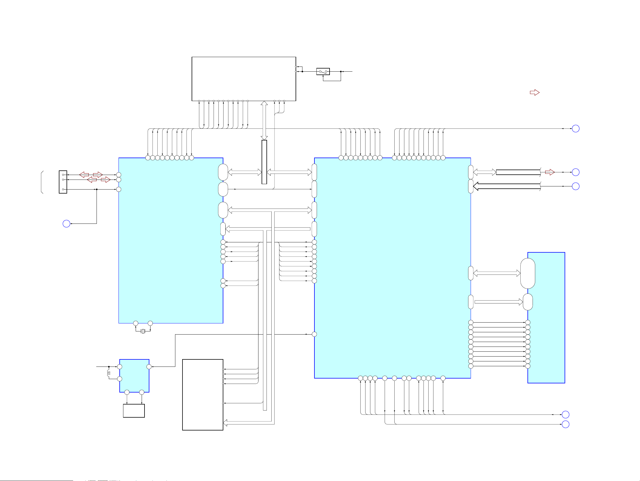
5-1. BLOCK DIAGRAM – MAIN Section (1/2) –
CN9502 (1/2)
USB
CRADLE
CONNECTOR
DATA+
DATA–
VBUS
DP
8
DM
10
14
VBUS
SECTION 5
DIAGRAMS
XHIOR
XHIOW
HIORDY
HDMARQ
71
72
73
XHIOW
HDMARQ
74
XHIOR
XHDMACK
77
HIORDY
XHCS0
HNTRQ
78
83
XHCS0
HINTRQ
XHDMACK
XHCS1
84
XHCS1
XHDASP
XHPDIAG
85
81
XHDASP
XHRESET
XHRESET
XHPDIAG
HDMARQ
XHIOW
HDMARQ
XHIOW
HDD0
HDA0ıHDA2
XHIOR
XHIOR
ı
HIORDY
HIORDY
HDD15
HARD DISK
DRIVE UNIT
XHDMCK
HINTREQ
XHCS0
XHC1
XDASP
XPDIAG
XHDMACK
HNTRQ
XHCS0
XHCS1
XHDASP
XHPDIAG
D0 – 15
53 – 60,
62 – 69
A0 – 2 A0 – 2
82
81, 79,
H_D0
H_D15
D0 – 15
DATA BUS
VDC (MOTOR)
VDC (LOGIC)
H_A0
H_A1
H_A2
A0A1A2
D0 – 15
B+ SWITCH
Q2001
ı
HD0
124 – 139
HA0ıHA2
121 – 123
HD15
HDMARQ
XHRESET
148
146
XHRESET
+3.3V_HDD
XHIOR
XHIOW
143
142
XHIOW
HDMARQ
HIORDY
144
XHIOR
HNTRQ
XHDMACK
145
147
HIORDY
XHDMACK
XHCS1
XHCS0
141
140
XHCS1
HINTREQ
XHCS0
IC1001_XCS5
IC1001_XCS6
IC1001_XCS7
47
48
49
XCS1
XCS2
XCS3
IC1001_XRE
IC1001_XWE
IC1001_XLWR
50
51
52
XRD
XWR
XINTREQG
IC1001_WAIT
IC1001_XUWR
53
54
57
XLB
XUB
XWAIT
XINTREQH
XINTREQU
58
59
XINTREQG
XINTREQH
XINTREQU
31 – 46
D0 – D15
8 – 30
A1 –A 23
D0 – 15
A1 – 23
DATA BUS
ADDRESS BUS
• SIGNAL PATH
: AUDIO
IC1003 – IC7001
D0 – 15
A1 – 23
B
C
D
(Page 17)
(Page 17)
(Page 17)
(Page 18)
D0 – 7
37 – 40
32 – 35,
VBUS
A
USB
CONTROLLER
IC2001
XI
X2001
12MHz
ENA+3.3V 3
OUT2
5
XO
100
LIQUID
CRYSTAL
DISPLAY
UNIT
BACK LIGHT
VDD4
8 LDR
OUT1
BACK LIGHT
DRIVER
IC5001
6
99
EL
UNIT
CD0 – CD7
A0 – 7
17 – 24
CA0 – CA7
XCS 27 XUCS0115
XWAIT 29
XWR 30
XINT
31
XRESET 15
XSLEEP 16
CS
WR
RD
RESET
RS
DB8 – 15
XUCS0
XURD
XUWAIT
XUWR
XUINTREQ
XRESET
XSLEEP
XUCS1
XUWR
XURD
XRESET_LCD
D0 – 7
XUCS0
XUCS1
XURD
XUWR
XUWAIT
XUINTREQ
XRESET_LCD
XRESET
XSLEEP
A0
107 – 114
99 – 106
116XRD 28
117
118
119
120
161
155
156
UD0 – UD7
UA0 – UA7
XUCS1
XURD
XUWR
XUWAIT
XUINTREQ
RESET_LCD
URESET
USLEEP
BACKLIT_PWR159
EXCLKIN
7
153
XOUT
FS256
FS256
XICKSTP6XRESET
173
SLEEP
XRESET
MULTI INTERFACE
IC7001
D33_MODE
GSEN_PWR_CTL
160
158
D33_MODE
GSEN_PWR
CLK2250A4CLK2250X
3
EXT_CLK
XEXT_CLK
XRDE
DATA
152
151
150
CDIF_XRDE
CDIF_PCMD
CDIF_BCK
BCK
LRCK
149
CDIF_LRCK
D0 – 15
75 – 90
SD0 – SD15
A0 – 12
60 – 72
SA0 – SA12
BA0 73 20
BA1 74 21
XSCS 91 19
XRAS 92 18
XCAS 93 17
XSWE 94 16
LDQM 95 15
UDQM 96 39
SDCLK 97 38
SDCKE
DTCK
154
RMC_DTCK
SD-RAM
IC7002
DQ0 – 15
2, 4, 5, 7, 8, 10,
47, 48, 50, 51, 53
11, 13, 42, 44, 45,
A0 – 12
22 – 26,
29 – 36
BA0
BA1
XCS
XRAS
XCAS
XWE
LDQM
UDQM
CLK
37
CKE98
IC3001 – IC7001
D33_MODE, GSEN_PWR
E
F
(Page 17)
(Page 18)
NW-HD1
1616
Page 17
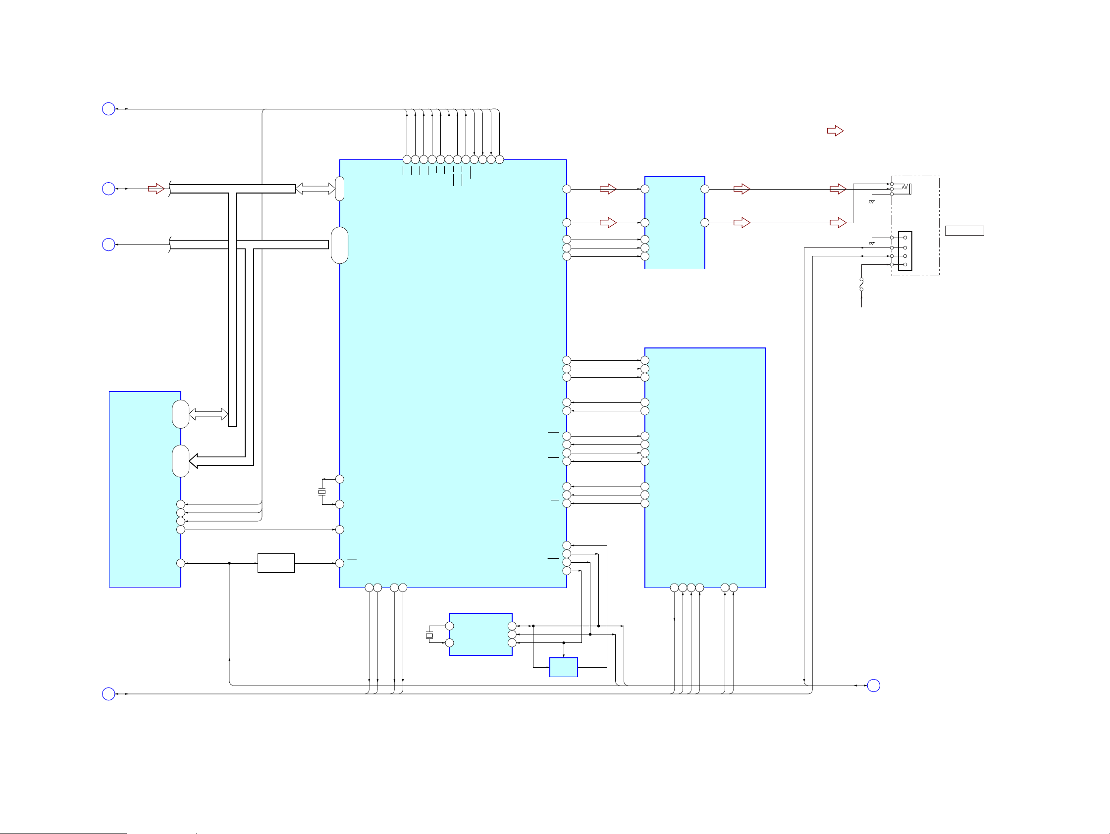
5-2. BLOCK DIAGRAM – MAIN Section (2/2) –
NW-HD1
(Page 16)
(Page 16)
(Page 16)
B
C
D
IC1003 – IC7001
D0 – 15
A1 – 23
FLASH MEMORY
IC1101
DATA BUS
ADDRESS BUS
D0 – 15
38 – 45
29 – 36,
DQ0 – DQ15
A1 – 20
16 – 25
A1 – A20
48, 1 – 9,
XCE
26
XOE
28
XWE
11
R/XB 15
XRST
12 RST106
IC1001_XCS0
IC1001_XRE
IC1001_XUWR
LEVEL SHIFT
Q1001
A1 – 23
X1002
22.5792MHz
D0 – 15
38 – 53
PO0/D0 – P07/D7,
2 – 13
197 – 207,
137
XTAL
138
EXTAL
PG0/DAKC086
PB0/D8 – PB7/D15
PL1/A1 – PL7/A7,
PN0/A16 – PN7/A23
PM0/A8 – PM7/A15,
XOUT/CK0
P14/FS256
77
175
IC1001_XCS0
IC1001_XCS5
IC1001_XCS6
186
191
192
PK0/CS0
PK5/CS5
PK6/CS6
MAIN SYSTEM CONTROLLER,
PQ5
PQ7
151
153
IC1001_XRE
IC1001_XWE
IC1001_XCS7
IC1001_XLWR
193
182
185
183
PJ1/RE
PJ4/WE
PK7/CS7
D/A CONVERTER
IC1003 (1/2)
XINTREQH
XINTREQG
IC1001_WAIT
IC1001_XUWR
184
181
88
89 83
PJ0/WAIT
PJ2/LWR/LB
PJ3/UWR/UB
PG2/DACK1/INT6
PG3/DREQ1/INT7
REAL TIME CLOCK
IC9503
XINTREQU
PF2/EC2/INT4
AOUTL 134
AOUTR 133
PF4/BEEP 85
PR7 163
PR6 162
PP1/RB 34 PF236
PP0/RP 33
PQ6 152
PG1/DREQ0/INT5 87
PF0/EC0/INT3 81
PC3/SCS0 60
PC2/SI0 59
PC1/SO0 58
PC0/SCK0 57
PI1/ADDT 172 P10/PCMD015
PI2/LRCK 173
PI3/BCK 174
PE6/SI1 75
PE5/SO1 74
PE4/SCK1 73
PE7/SCS1
76
BEEP
HP_MUTE
HP_LINE_SEL
SREQ
WAKEUP
XRESET
DATA_READY
XINT
SS
SO
SCLK
GDAC_PCM0
GDAC_LRCK
GDAC_BCK
• SIGNAL PATH
: AUDIO
HEADPHONE AMP
IC4301
L-IN3
R-IN1
BEEP14
MUTE15
16
HP/L
PF034
NRST
33
PF135
PF3
37
SI
40
38
13
PC342
PC1
PC241
PC0
P12/LRCK014
P13/BCK0
PF4/XRDE
12
4
LOUT 10
ROUT 12
SUB SYSTEM
CONTROLLER
IC3001
BCK1LRCK
PCMD
2
XTAL29EXTAL
30
F4301
+2.4V_AD
RM_GND
RM_KEY
RM_TSB
RM_VDD
J4301
/LINE OUT
i
NW-HD1
(Page 16)
E
IC3001 – IC7001
XRST
XOUT
FS256
SLEEP
XRESET
X9501
32kHz
OSC OUT8
OSC IN7
SIO 1
SCLK 2
CE 12
BUFFER
IC9502
MULTI_SCK
MULTI_SO
CDIF_PCMD
CDIF_XRDE
CDIF_BCK
CDIF_LRCK
XEXT_CLK
EXT_CLK
PMC_DTCK
AD_RMKEY
MULTI_SIO
G
(Page 18)
1717
Page 18
NW-HD1
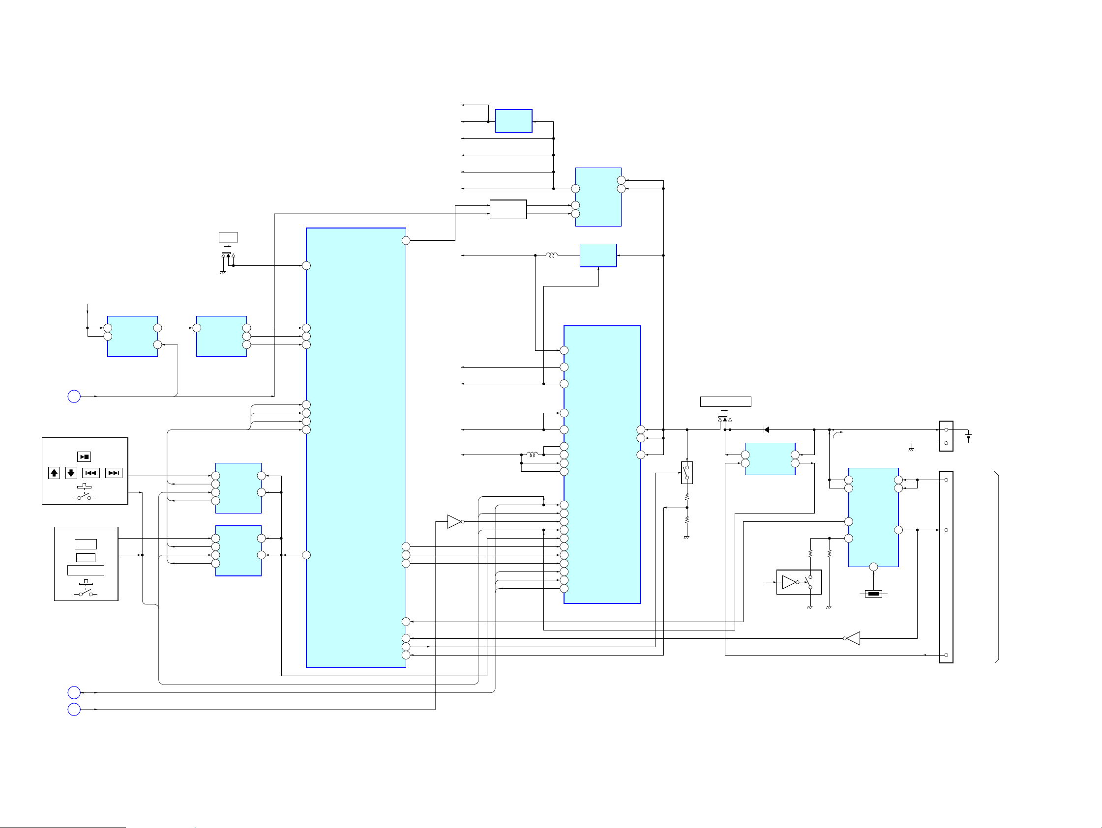
5-3. BLOCK DIAGRAM – KEY/POWER SUPPLY Section –
S5009
HOLD
ON OFF
+2.4V_AD
(IC1003)
+2.4V_DAC
(IC1003)
+3.3V
(IC4301)
+3.3V_HD
+3.3V_A
PF1/T1 82
+2.8V
P17170
+2.4V
REGULATOR
IC4302
BUFFER
Q9002, 9004
DC/DC CONVERTER
IC9001
PVIN
VOUT+3.3V
8
XSHDN/SS1
MD/SYNC7
SWITCHING
REGULATOR
IC9003
EN
VIN
9
10
(Page 16)
+3.3V
D33_MODE, GSEN_PWR
F
SWITCH UNIT
,
SWITCH UNIT
SET UP
,
MODE
VOLUME +/–
B+ SWITCH
IC8001
3.3V1
G_VDD 2
VDD5
,,,
,
PD 4
GSEN_PWR
KEY2
XCHG_PG
PQ4
KEY1
RMCKEY
RMC (K1)
SET_KEY
G-SENSOR
IC8000
VDD6 AOUTX 8
D33_MODE
1A1
1B2
2A5
2B6
1A1
1B2
2A5
2B
6
AOUTY 9
AOUTZ 10
KEY SELECT
SWITCH
IC1001
KEY SELECT
SWITCH
IC1002
1C 7
2C
1C 7
2C 3
KEY2
PQ4
KEY1
RMC (K1)
3
POWER
CONTROL
REGI348
REGO347
REGO154
REGI1
VCO111
L237
L238
VCIN41
VC242
XWK1
XWK24
XWK33
XWK42
FFCLR
SLEEP
CLK
STRB
DATA
SCK
XRST2
IC9002
VB 27
LG 25
VO2 39
S9501
BUILT-IN BATTERY
ON OFF
BATTERY
MONITOR
SWITCH
Q9001,
9503
D9501
OUT7
IN2 6
IN18
STAT 1
AUTO SELECT
POWER SWITCH
IC9504
+2.4V
CHARGE
CURRENT
SWITCH
Q9501
CONTROL
OUT10 IN
BAT9
STAT24
ISET
5
TEMPERATURE
Q9502
CHARGE
IC9501
TS
8
DETECT
TH9501
VCC 2
STAT1 3
CN9501
BATT+
BATT–CHARGE
CN9502 (2/2)
1
LITHIUM ION
BATTERY
LIS1317HNP
4.2V 760mAh
DC IN 6V
XCHG_STAT1
DC5V
USB
CRADLE
CONNECTOR
AN2
100
AN3101
AN4102
MAIN SYTEM
CONTROLLER
IC1003 (2/2)
AN5
103
PQ4150
AN6/INT8104
AN7/INT9105
PQ1/PGMTR1147
PQ0/PGMTR0 146
PF3/T3 84
PE2/TXD1 71
PQ3/PGMTR3 149
PQ2/PGMTR2 148
PR0 156
AN0 98
+1.5V
+2.0V
+2.4V
+1.2V
Q9003
RMCKEY
AD_RMCKEY
SET_KEY
XCHG_PG
MULTI_SO
MULTI_SCK
XRST
55
5
1
64
63
59
58
60
34
(Page 17)
(Page 16)
NW-HD1
G
A
MULTI_SIO
VBUS
1818
Page 19
NW-HD1
e
Ver 1.1
• Note for Printed Wiring Boards and Schematic Diagrams
Note on Printed Wiring Board:
• X : parts extracted from the component side.
• Y : parts extracted from the conductor side.
• f : internal component.
• : Pattern from the side which enables seeing.
(The other layers' patterns are not indicated.)
Caution:
Pattern face side: Parts on the pattern face side seen from
(Conductor Side) the pattern face are indicated.
Parts face side: Parts on the parts face side seen from
(Component Side) the parts face are indicated.
• MAIN and HDD boards are multi-layer printed board.
However, the patterns of intermediate-layer have not been included in diagram.
*Replacement of IC1003, 1101, 2001, 3001, 7001 and 7002
used in this set requires a special tool.
• Lead Layouts
surfac
Lead layout of conv entional IC CSP (chip size package)
Note on Schematic Diagram:
• All capacitors are in µF unless otherwise noted. (p: pF)
50 WV or less are not indicated except for electrolytics
and tantalums.
• All resistors are in Ω and 1/
specified.
• f : internal component.
• C : panel designation.
Note:
The components identified by mark 0 or dotted
line with mark 0 are critical for safety.
Replace only with part
number specified.
• A : B+ Line.
• Power voltage is dc 4.2 V and fed with regulated dc pow er
supply from CN9501.
• Voltages and waveforms are dc with respect to ground
under no-signal conditions.
no mark : PLAYBACK
• Voltages are taken with a VOM (Input impedance 10 MΩ).
Voltage variations may be noted due to normal production tolerances.
• Waveforms are taken with a oscilloscope.
Voltage variations may be noted due to normal production tolerances.
• Circled numbers refer to waveforms.
• Signal path.
F : AUDIO
*Replacement of IC1003, 1101, 2001, 3001, 7001 and 7002
used in this set requires a special tool.
• The voltage and waveform of CSP (chip size package)
cannot be measured, because its lead layout is different
form that of conventional IC.
4
W or less unless otherwise
Note:
Les composants identifiés par
une marque 0 sont critiques
pour la sécurité.
Ne les remplacer que par une
pièce portant le numéro
spécifié.
• Waveform
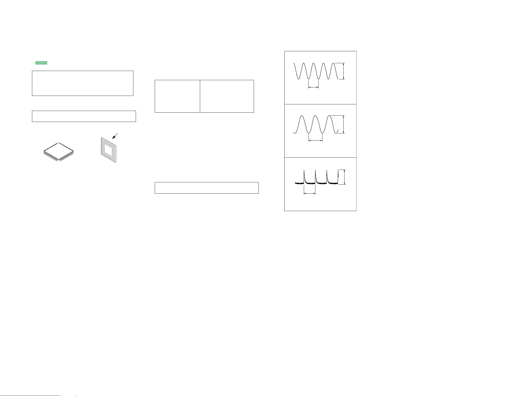
– MAIN Board –
X1002
1
44.3 ns
500 mV/DIV, 20 ns/DIV
IC9503 8 (OSCOUT)
2
30.5 µs
200 mV/DIV, 10 µs/DIV
IC9001 8 (VOUT)
3
304 µs
20 mV/DIV, 100 µs/DIV
1.9 Vp-p
1 Vp-p
80 mVp-p
NW-HD1
1919
Page 20
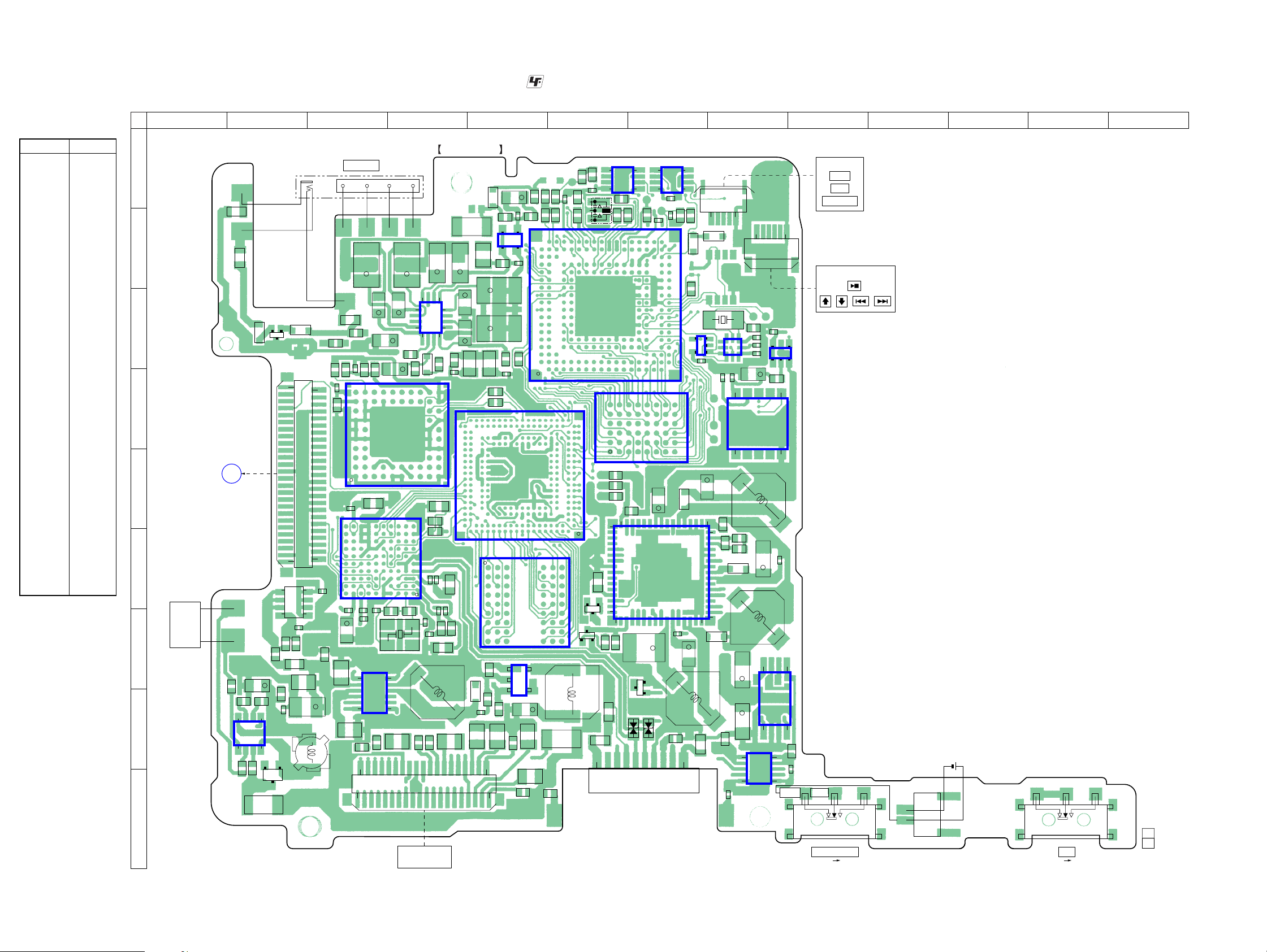
NW-HD1
• Semiconductor
Location
Ref. No. Location
D4101 C-2
D4201 C-2
D4301 C-4
D4302 C-2
D4445 A-5
D5001 B-8
D5002 B-7
D5003 I-2
D9001 F-8
D9002 G-8
D9003 E-7
D9005 H-5
D9006 I-9
D9501 I-9
IC1001 A-6
IC1002 A-7
IC1003 C-6
IC1101 D-7
IC2001 F-3
IC3001 D-4
IC4301 C-4
IC4302 B-5
IC5001 H-2
IC7001 E-5
IC7002 F-5
IC8000 D-8
IC8001 C-8
IC9001 H-3
IC9002 F-7
IC9003 G-5
IC9501 H-8
IC9502 C-7
IC9503 C-8
IC9504 H-8
Q2001 F-2
Q9001 F-6
Q9003 G-6
Q9502 G-7
VDR9503 H-7
VDR9504 H-7
5-4. PRINTED WIRING BOARD – MAIN Section (Component Side) –
1 2 3 4 5 6 7 8 9 10 11 12 13
J4301
i
A
FB4305
/LINE OUT
B
FB4201
D4101
AK
KAK
C
D4201
D4302
AK
R4105
R4205
CN2001
51
R3015
50
C3006
FB4101
R3004
C3003
C4204
+
C4308
VDR3002
VDR3001
C4105
C4205
+
+
IC4301
+
C4302
+
R4309
+
C4303
MAIN BOARD (COMPONENT SIDE)
D4445
F4301
L4301
C4307
C4309
C4104
85
9
12
13 16
D4301
+
+
+
+
4
C4304
C4301
+
L3001
+
L3002
1
C3013
AK
R4308
C3007
D
C3005
∗
IC3001
A
E
F
EL
BACK
LIGHT
UNIT
G
H
I
HDD BOARD
CN100
(Page 29)
SP5002
SP5001
R5005
R5023
41
58
R5004
C5019
R5002
R5003
C5015
1
4
R2011
R2046
+
R5024
C5020
IC5001
A
D5003
K
1
Q2001
FB9001
C9016
C9036
8
5
C2026
R2045
L5001
C2025
+
C2021
C2023
C2014
+
C2022
IC2001
C2012
C2019
∗
R2010
X2001
2
C2020
C9019
R2009
C2011
C2002
C2001
R2001
C2007
C2006
C2017
R2003
C2013
R2004
C2005
C2015
FB2001
IC9001
C5003
L9004
C5004C5001
D9005
C9024
KA
C5007
R9012
38
39
C9018
C9011
12
7
C5006
6
1
C5005
2
1
C5002
CN5001
LIQUID CRYSTAL
DISPLAY UNIT
AK
C4320
C4319
R4302
43
12
IC4302
C4318
R4301
C4316
C4317
R1026
R4307
C3008
R7012
R7011
IC7001
IC7002
IC9003
1
C9026
3
C9028
R9038
C5009
C5011
C5012
:Uses unleaded solder.
FB1011
R1022
R1027
FB1005
C1017
C1001
C1025
FB1004
X1002
+
R4316
R4313
R1029
R1028
IC1003
∗
∗
C5010
5
4
+
C5008
L9005
C5013
R9514
Q9001
Q9003
BCE
FB7001
FB7002
FB7003
FB9502
5
4
4
IC1002
C1021
C1027
R1207
851
C1002
C1022
C1026
VDR1001
VDR1002
CN5003
15
KA
AK
D5001
IC1001
8
R1002
1
D5002
∗
R1025
4
1
3
5
IC9502
C9504
IC9503
X9501
97
10
12
1
3
C8004
C8005
610
∗
IC1101
51
+
D9003
AK
C9029
48 33
49
C9014
+
IC9002
C9015
GDS
64
116
C9012
R9018
R9000
Q9502
VDR9504
C9501
1
CN9502
(USB CRADLE CONNECTOR)
GDS
VDR9503
C9006
+
C9502
C9010
C9008
32
R9006
C9005
R9004
D9001
17
AK
D9002
+
C9007
L9002
C9505
FB9501
10
1
5
C9517
1
CN5002
C9510
C9509
6
C9507
4
C9506
+
C8007
IC8000
L9003
C9003
+
KA
L9001
8
C9515
+
+
C9514
14
IC9501
C8006
R8002
C9511
6
45
31
C9002
5
IC9504
10
C9503
6
KA
D9501
SWITCH UNIT
IC8001
R9515
BUILT-IN BATTERY
OFF ON
SET UP
MODE ,
VOLUME +/–
SWITCH UNIT
S9501
,
,
,,,
LITHIUM ION
BATTERY
LIS1317HNP
4.2V 760mAh
CN9501
2
1
11
S5009
HOLD
OFF ON
1-862-777-
(11)
NW-HD1
2020
Page 21
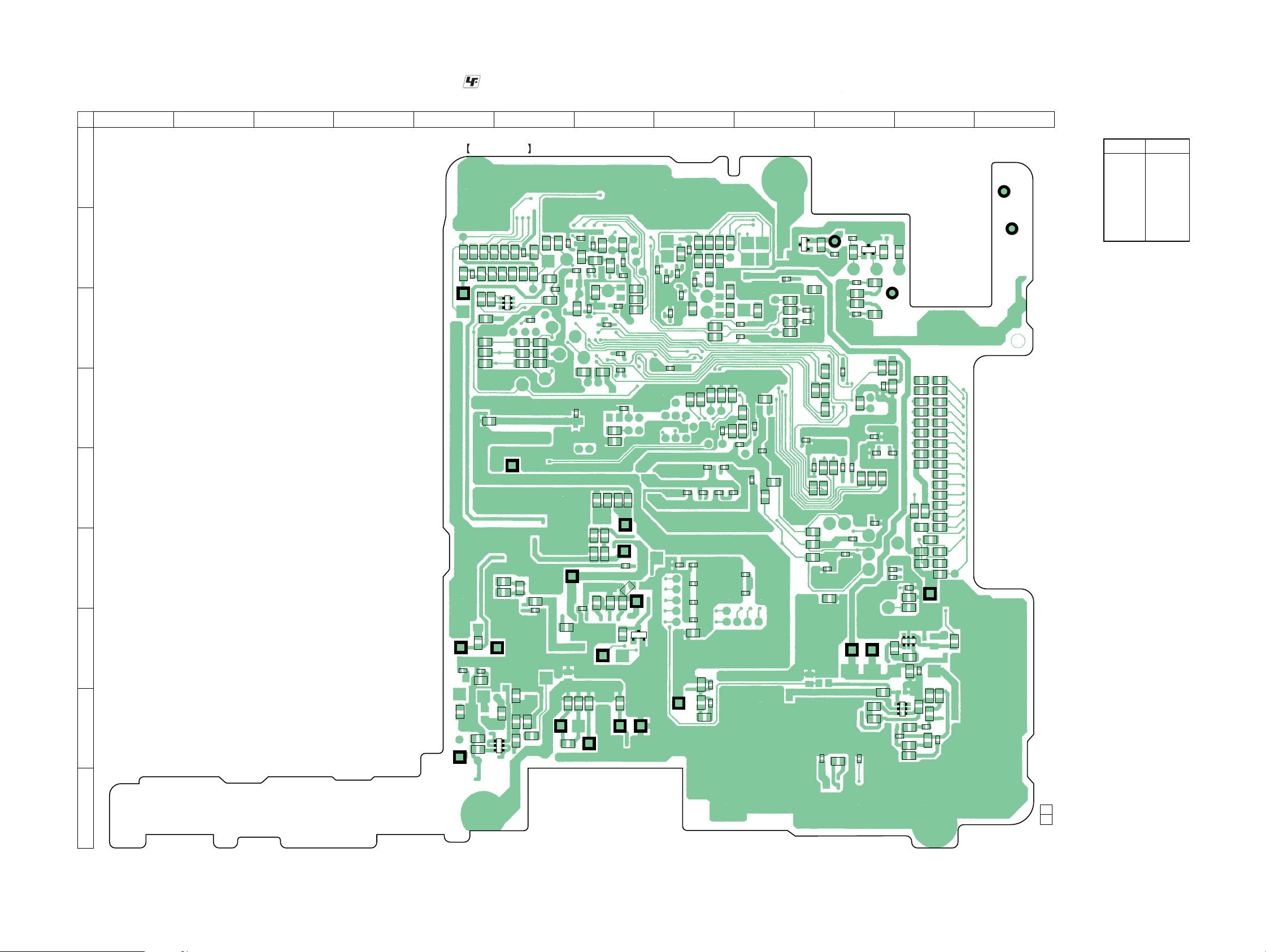
NW-HD1
5-5. PRINTED WIRING BOARD – MAIN Section (Conductor Side) –
1 2 3 4 5 6 7 8 9 10 11 12
A
B
C
D
E
F
G
H
:Uses unleaded solder.
MAIN BOARD
R5009
R5011
R5015
R5017
R5020
R5022
R5008
R5014
R5012
R5010
R5016
R1111
TP5002
TP5003
C9513
R9509
TP9502
R8001
C8003
C8002
C8001
R1110
C9512
R9513
R9503
R9505
C5017
FB1101
R5018
TP9513
2C
1B
1C
Q9501
2C
2E
1C
Q1001
R8008
C9004
R9005
R9507
TP9002
R9501
2B
2E
1E
2B
1E
1B
R5019
C9508
R9003
TH9501
R9506
R9504
(CONDUCTOR SIDE)
R1047
R1019
C1019
C1015
R5013
C5018
R8005
R8006R8009
R8007R8010
TP9511
C1013
TP9001
C9009
VDR9501
VDR9507
R9512
R9002
FB1006
C1103
C9013
TP9506
R9007
C9001
R1015
C1030
R5021
R1018
R9502
C1014
R9023
C9022
TP9004
C1016
C1009
C1006
FB1002FB1001
R9024
R9015
R1204
R9001
R1009
C1008
C1005
C1004
R9022
R9014
VDR9502
R9029
C1101
R9021
R9020
R9019
C9020
R9511
R1102
R1103
TP9013
R9016
R1023
C1028
C1020
C9023
TP9003
TP9006
R9031
Q9503
BCE
VDR9506
TP9504TP9510
R1205
R1203
R1206
C1024
C1007
C1023
C1003
TP9007
C1010
C7015
R1202
C1012
C7002
FB7004
C1018
R1013
C4101
C4201
R7004
C7007
R9009
R9030
R1201
R1016
C1011
R1021
C7016
C7017
C7018
C7014
R9036
R7003
R1011
R1007
R7005
C7003
R1008
C7011
C7005C7006
C9032C9027
R7002
C7008
R4002
R1017
C4102
C4202
R7001
VDR7001
C7009
C7013
C7012
R1006
R1005
R1001
R7006
C7001
VDR7002
C7010
C7004
R4102
R4101
R4201
R4202
R7009
R7010
C4306
R7008
D4303
A
R2008
R2006
R2007
C4103
C4203
C3010
K
K
R4305
R3005
C3012
R3019
C2008
TP4308
C4315
FB4301
R3021R3020
R2005
C5016
R4104
R4204
R3006
R3002
R3010
R3022
R5001
C2009
C4313
FB4303
C4106
C4206
C3018
C2010
R9008
R9013
C3004
C3015
D4304
KAK
R4103
C3009
R3023
C2018
TP9008TP9009
C5014
FB4302
TP4313
R4203
VDR3003
VDR3004C3002
R2043 R2044
R2041 R2042
C3001
R2039 R2040
R3014
R2037 R2038
R2035 R2036
R2033 R2034
R2031 R2032
R2029 R2030
C3011C3017
R2021 R2019
R3025
R3024
R2027
R2025
C2016
C2024
VDR2001
VDR2002
2B
R9041
R9037
Q9002
1B
1E
2B
R9033
C9021
R9028
R9010
FB4304
R2026
C2004
1E1B
2E1C2C
C9025
1C
2E
2C
R2022
TP2001
Q9004
R9040
C9030
R2023
C9037
R9032
C9031
R9035
R9011
C9017
R2018
R2017
R2016
R2015
R2014
R2028
R2013R2024
R2012
R2020
R9034
R9027
TP4312
TP4314
• Semiconductor
Location
Ref. No. Location
D4303 B-9
D4304 B-10
Q1001 C-6
Q9002 H-11
Q9004 G-11
Q9501 H-6
Q9503 G-7
NW-HD1
I
1-862-777-
11
(11)
2121
Page 22

NW-HD1
5-6. SCHEMATIC DIAGRAM – MAIN Section (1/7) –
(1/7)
U_A
U_D
USB_CNT
RMC_DTCK
(Page 28)
(Page 28)
BACKLIGHT_PWR
XRESET_LCD
D33_MODE
R7001
1k
R7002
100k
S_GOHAN
C7001
0.1
C7002
0.1
C7003
0.1
C7004
0.1
C7005
0.1
C7006
0.1
C7007
0.1
C7008
0.1
C7009
0.1
C7010
0.1
FB7001
FB7002
FB7003
VDR7001
100p
C7011
470k
R7006
3.3V
0
R7005
1.2V
1.8V
GND
VDR7002
(Page 24)
• See page 34 for IC Pin Function Description.
6
T
E
K
K
D
5
D
C
C
M
2
B
R
R
C
L
X
FS
P
_
IF_
IF
IF_
D
IF_
D
C
D
D
C
C
C
DTCK
A11
1
1
A
G
BCK
DATA
LRCK
XRDE
FS256
A16
A15
A14
A13
A12
2
3
4
5
6
1
1
1
1
1
A
A
A
A
A
G
G
G
G
G
R7003 R7004 R7008
1k 1k 0
S
TDI
TCK
TDO
TM
TRST
TEST0
TEST1
TEST2
XICKSTP
NC
VDD12
VDD12
VDD12
VDD12
VDD12
VDD12
VDD12
VDD12
VDD12
VDD12
VDD12
VDD12
VDD12
VDD12
VDD12
VDD12
VDE18
VDE18
VDE18
VDE18
VDE18
VDE18
VDE18
VDE18
VDE18
VDE18
VDE33
VDE33
VDE33
VDE33
VDE33
VDE33
GND
GND
GND
GND
GND
GND
GND
GND
GND
GND
GND
GND
GND
GND
GND
GND
GND
NC
NC
NC
NC
NC
XRESET
EXCLKIN
XOSCSTP
CLK2250X
CLK2250A
EXTAL
XTAL
EXT_CLK
XEXT_CLK
T
U
O
X
XRESET_GOHAN
P
N
E
E
E
S
E
S
E
L
G
S
R
X
U
U
X
X
GPIO8
A2
R
ODE
R_CTL
R_CTL
R_CTL
USLEEP
BACKLIT_PW
GSEN_PW
A6A7A8
7
A
G
8
A
G
HDD_PW
9
A
G
URESET
A10
A9
0
1
A
G
D33_M
RESET_LCD
XEL_PW
A5
A4
A3
3
4
5
6
A
A
A
A
G
G
G
G
ODE
SYNCM
A1
1
2
A
A
G
G
T
E
S
E
R
H
X
7
1
A
G
XHRESET
A17
Q
Q
E
E
R
R
T
A
M
IN
D
H
H
ARQ
HINTREQ
HDM
CSP(Chip Size Package)
A19
A18
8
9
1
1
A
A
G
G
K
Y
C
D
A
R
M
IO
D
H
H
X
X
HIORDY
XHDMACK
MULTI INTERFACE
IC7001
CXD1616GH
A21
A20
0
1
2
2
A
A
G
G
470k470k
R7010R7009
SD-RAM
IC7002
HDD_CNT
H_D
H_A
XGSEN_PWR_CTL
XUSLEEP
XURESET
USB_CNT
U_D
U_A
∗
-E
FS256
GANDHI_CNT
GAND_D
GAND_A
XRESET_GOHAN
SLEEP_GOHAN
XOUT
XINTREQU
XINTREQH
XINTREQG
XEXT_CLK
EXT_CLK
CDIF_XRDE
CDIF_PCMD
CDIF_BCK
CDIF_LRCK
GANDHI_CNT
GAND_D
GAND_A
(Page 26)
SD15
SD14
SD13
SD12
SD11
SD10
SD9
UDQM
SDCLK
SDCKE
SA12
SA11
SA9
SA8
SA7
SA6
SA5
(Page 25)
(Page 23)
1
0
R
W
S
S
IO
C
C
IO
H
X
XHIOW
∗
A22
2
2
A
G
H
X
XHIOR
A23D0D
3
2
A
G
4
5
H
H
1
1
X
X
D
D
H
H
HD15
XHCS1
XHCS0
1
D2
0
1
2
3
D
D
D
D
G
G
G
G
0
1
2
3
1
1
1
1
D
D
D
D
H
H
H
H
12
14
HD10
HD11
HD
HD13
HD
6
7
D
D5
D4
D3
D
4
5
6
7
D
D
D
D
G
G
G
G
5
6
7
8
9
D
D
D
D
D
H
H
H
H
H
HD5
HD6
HD9
HD7
HD8
9
10
12
D8
D
D
D
D11
0
1
2
8
9
1
1
1
D
D
D
D
D
G
G
G
G
G
0
1
2
3
4
D
D
D
D
D
H
H
H
H
H
HD2
HD3
HD4
15
D
D14
D13
3
5
1
14
1
D
D
D
G
G
G
0
1
2
A
A
A
H
H
H
Q
E
R
T
IN
U
X
HA0
HA1
HA2
HD1
HDO
XUINTREQ
R
XW
XRD
XCS3
XCS1
XCS2
XLB
5
6
7
R
D
S
S
S
C
X
B
C
C
R
W
L
X
X
X
X
X
0
1
R
D
IT
S
S
R
A
W
C
C
U
W
U
U
X
XU
U
X
X
X
R
RD
XU
XUW
XUCS1
XUCS0
XUWAIT
AIT
XW
XUB
IT
A
B
U
W
X
X
UD7
UD6
UD5
UD4
UD3
UD2
UD1
UD0
UA7
UA6
UA5
UA4
UA3
UA2
UA1
UA0
SDCKE
SDCLK
UDQM
LDQM
XSWE
XCAS
XRAS
XSCS
SD15
SD14
SD13
SD12
SD11
SD10
SD9
SD8
SD7
SD6
SD5
SD4
SD3
SD2
SD1
SD0
BA1
BA0
SA12
SA11
SA10
SA9
SA8
SA7
SA6
SA5
SA4
SA3
SA2
SA1
SA0
XINTREQU
XINTREQH
XINTREQG
NC
NC
UD7
UD6
UD5
UD4
UD3
UD2
UD1
UD0
XINTREQU
XINTREQH
XINTREQG
UA7
UA6
UA5
UA4
UA3
UA2
UA1
UA0
SDCKE
SDCLK
UDQM
LDQM
XWE
XCAS
XRAS
XCS
SD15
SD14
SD13
SD12
SD11
SD10
SD9
SD8
SD7
SD6
SD5
SD4
SD3
SD2
SD1
SD0
BA1
BA0
SA12
SA11
SA10
SA9
SA8
SA7
SA6
SA5
SA4
SA3
SA2
SA1
SA0
FB7004
C7012
C7013
C7014
C7015
C7016
C7017
C7018
0.1
0.1
0.1
0.1
0.1
0.1
0.1
XGSEN
XUSLEEP
XURESET
EDL1216CASA-10L
CSP(Chip Size Package)
SD0
SD1
SD2
SD3
SD4
SD5
SD6
SD7 SD8
LDQM
XWE
XCAS
XRAS
XCS
BA0
BA1
SA10
SA0
SA1
SA2
SA3 SA4
FS256
XRESET_GOHAN
S_GOHAN
XOUT
XINTREQU
XINTREQH
XINTREQG
22
XEXT_CLK
EXT_CLK
CDIF_XRDE
CDIF_PCMD
CDIF_BCK
CDIF_LRCK
R7012
R7011
22
NW-HD1
2222
Page 23

NW-HD1
5-7. SCHEMATIC DIAGRAM – MAIN Section (2/7) –
(2/7)
(Page 22)
GANDHI_CNT
XEXT_CLK
GAND_D
GAND_A
EXT_CLK
• See page 30 for IC Block Diagram.
XUWR
GA1
GA17
R1102
0
CSP(Chip Size Package)
GA16
GA15
GA14
GA13
GA12
GA11
GA10
GA9
GA20
C1101
100p
GA19
R1103
GA18
100k
GA8
GA7
GA6
GA5
GA4
GA3
GA2
L3001 100µH
100µH
0.1
0.1
08
07
30
30
C
C
L3002
FLASH MEMORY
IC1101
MBM29SL800BE
-90PT
(NOT SUPPLIED)
A15
A14
A13
A12
A11
A10
A9
A8
NC
NC
XWE
XRST
NC
NC
R/XB
A18
A17
A7
A6
A5
A4
A3
A2
A1
XRE
XCS0
∗
A16
XBYTE
VSS
DQ15
DQ7
DQ14
DQ6
DQ13
DQ5
DQ12
DQ4
VCC
DQ11
DQ3
DQ10
DQ2
DQ9
DQ1
DQ8
DQ0
XOE
VSS
XCE
A0
GD15
GD7
GD14
GD6
GD13
GD5
GD12
GD4
C1103
GD11
GD3
GD10
GD2
GD9
GD1
GD8
GD0
C3010
0.1
0.1
1101
FB
RDY_XBUSY
XRESET_1.8V
DENDE_COMAND
(Page 28)
CDIF_LRCK
CDIF_BCK
CDIF_PCMD
CDIF_XRDE
VDR3001
VDR3002
C3012
C3003
100p
R3004
R3006
220
XRESET_D
WAKEUP_D
DATA_R
DENDE_S
XINT_D
R3002 R3010
470k 470k
GND
1.5V
3.3V
1.8V
470k
R3005
0
DENDE_SCLK
DENDE_SI
DENDE_SO
DENDE_SS
VDR3003
C3004
0.1
VDR3004
R3014
0
R3015
0
C3001
0.1
C3002
1
NRST
PF0
PF1
PF2
PF3
PC0
VDIOCD2
PC1
PC2
PC3
DVDD2
DVSS2
PE0
PE1
PE2
PE3
OSSEL
VDIO2
XIN
TACK(TEST6)
C3005
1
C3006
0.1
XTAL
EXTAL
TRST(TEST4)
XOUT(TEST5)
AVDMO
AVSPLL
AVSOSC
SUB SYSTEM
CONTROLLER
CXR710160-211GH
CSP(Chip Size Package)
TEST1
TEST2
TEST3
IC3001
AVDPLL
DVDD3
KDI
KCS
KRB
KDO
KCLK
DVDD1
TEST0
VDIO1
EVA
PI0/PCMDO
P12/LRCKO
PI3/BCKO
PF4/XRDE
VDIOCD1
VDIO0
DVSS0
DVDD0
TEST7
TEST8
DVDD4
PCMD
VDIOCD0
BCK
LRCK
TDO
NTRST
TMS
VDIO3
TDI
TCK
C3011
0.1
C3009
C3015
0.1
0.1
R3025
0
DVSS3
∗
DVSS1
0.1
C3013
R3019
R3020
R3021
R3022
R3023
R3024
1
0
0
0
0
0
0
C3018
0.1
C3017
0.1
XINT_D
DATA_R
DENDE_S
WAKEUP_D
XRESET_D
XINT_DENDE
DATA_READY
DENDE_SREQ
WAKEUP_DENDE
XRESET_DENDE
GDAC_PCMD
GDAC_LRCK
GDAC_BCK
(Page 25)
NW-HD1
2323
Page 24

NW-HD1
Ver 1.1
5-8. SCHEMATIC DIAGRAM – MAIN Section (3/7) –
• See page 30 for IC Block Diagrams.
LIQUID
CRYSTAL
DISPLAY
UNIT
EL
BACK LIGHT UNIT
DB15
DB14
DB13
DB12
DB11
DB10
DB9
DB8
RESET
CS
RS
WR
RD
GND
OSC2
OSC1
VCC
VCI
VREG
C6+
C6-
C5+
C5-
C4+
C4-
C3+
C3-
C2+
C2-
C1+
C1-
VLOUT
VLPS
VLREF
V1OUT
V2OUT
V3OUT
V4OUT
V5OUT
AD_RMCKEY
SET_KEY
SP5002
SP5001
CN5001
(3/7)
OFF ON
39P
UD7
UD6
UD5
UD4
UD3
UD2
UD1
UD0
XUCS1
UA0
XUWR
XURD
C5007
C5008
C5009
C5010
C5011
C5012
R5001
200k
C5014
1000p
C5016
0.1
C5001
1
C5002
1
C5003
1
C5004
1
C5005
1
C5006
1
C5013
1
0.1
0.47
0.47
0.47
0.47
0.47
S5009
HOLD
C5017 D5001
0.01 MA2S728-TX
R5010 R5014R5008 R5016
3.3k 1.5k6.8k 1k
C5018 D5002
0.01 MA2S728-TX
R5009 R5011
6.8k 3.3k
R5002
120k
R5018
470k
R5012
1M
R5013
1M
R5015 R5017
1.5k 1k
BACK LIGHT DRIVER
IC5001
SM8142BD-G-EL
VSS
OSC
ENA
VDD
TP5003
TP5002
R5019
680
4.7k
6.3V
10
C5019
R5024
R5021
R5022
4.7k
10
1k
R4313
R5020
680
L5001
D5003
1SS370
220µH
0.1
C5020
LDR
CHV
OUT1
OUT2
R5003
R5004
R5005
18k
0
C5015
0.1
0
R5023
470k
HOLD_KEY
AD_KEY2
AD_KEY1
CN5002
CN5003
BACKLIGHT_PWR
RMC_DTCK
XRESET_LCD
U_D
USB_CNT
U_A
6P
REPEAT
PLAY/STOP
DOWN
UP
SKIP
GND
5P
GND
SETUP
DISPLAY
VOL-
VOL+
(Page 22)
SET UP
MODE
VOLUME+/-
NW-HD1
(Page 28)
(Page 25)
(Page 28) (Page 25)
AD_RMCKEY
HP_LINE_SEL
HOLD_KEY
HP_MUTE
AD_KEY1
AD_KEY2
3.3V_A
AOUTR
AOUTL
VSTBY
0
BEEP
HOLD_KEY
AD_KEY1
AD_KEY2
C4202
2200p
R4202
12k
C4201
R4201
1
15k
C4101
1
R4101
15k
R4102
12k
C4102
2200p
GND
L4301
R4301
100µH
1.2V
3.3V
R4305
R4309
10k
R4308
150k
R4307
C4301
10 6.3V
C4302
1 6.3V
C4303
1
C4203
470p
C4103
470p
C4304
22
4V
10
1
C4316 C4317 C4307
47
6.3V476.3V
MA2S728-TX
D4301
R-IN
GND GND
L-IN
RIP-F1
C4306
47
0.01
6.3V
HP/L
MUTE
HEADPHONE AMP
IC4301
AN17020A-VB
VCC1
CR
C4308 C4309
224V47
BEEP
RIP-F2
C4205
2.2
6.3V
GA-R
ROUT
LOUT
GA-L
VCC2
4V
C4318
C4204
220 2.5V
C4104
220 2.5V
C4105
2.2 6.3V
C4206 C4106
0.01 0.01
0.1
VDD
VOUT
+2.4V REGULATOR
IC4302
R1180Q241B-TR-FA
GND
CE
R4105
0
R4103R4203
10k
10k
2222
R4104
R4204
R4316
22
C4320
C4319
10
0.1
6.3V
R4205
D4445
MA2S728-TX
F4301
R4002
250mA
1M
125V
FB4301
FB4302
100
FB4303
FB4304
FB4305
0
R4302
0.01
C4313
0
MA2S111-TX MA2S111-TX
1000p
C4315
D4101 D4201
D4302 D4303 D4304
MAZW068H0LS0 MAZW068H0LS0 MAZW068H0LS0
FB4101
FB4201
TP4308
TP4312
TP4313
TP4314
RM_VDD
RM_TSB
RM_KEY
RM_GND
The components identified by mark 0 or dotted
line with mark 0 are critical for safety.
2424
Replace only with part number specified.
J4301
/LINE OUT
2.4V_AD
2.4V_DAC
GND_A
Les composants identifiés par une marque 0 sont
critiques pour la sécurité. Ne les remplacer que
par une pièce portant le numéro spécifié.
Page 25

NW-HD1
5-9. SCHEMATIC DIAGRAM – MAIN Section (4/7) –
(4/7)
3.3V
1.8V
1.2V
GND
XCHG_STAT1
XCHG_STAT2
MULTI_SIO
XCHG_PG
XCHG_PG
PWR_FFCLR
MULTI_SIO
PWR_SLEEP
BATT_MON_CTL
PWR_CLK
PWR_STRB
AD_GSEN_X
AD_GSEN_Y
AD_GSEN_Z
RTC_CE
AD_BATT
VSTBY
KEY SELECT SWITCH
IC1001
SN74LVC2G66DCUR
KEY2
PPGM2
PPGM3
PGM0
PR0
PF3
PE7
XRST
AD_BATT
AD_GSEN_X
AD_GSEN_Y
AD_GSEN_Z
PE2
KEY1
C1001
C1002
GND
0.1
0.1
KEY SELECT SWITCH
IC1002
SN74LVC2G66DCUR
GND
R1015
VCC
VCC
0
AD_RMCKEY_1AD_KEY1_1
(Page 28)
(Page 27)
(Page 28)
(Page 26)
• See page 19 for Waveform. • See page 34 for IC Pin Function Description.
GA3
GA4
GA1
GA5
GA2
GA6
GA7
GA9
C1010
0.1
C1007
0.1
C1003
0.1
GA12
GA13
GA14
GA15
GA16
GA17
GA18
GA19
GA20
GA21
GA22
GA23
FB1001
FB1002
PP0
PP1
C1005
0.1
GD0
C1004
0.1
GD1
GD2
C1011
0.1
GD3
GD4
GD5
GD6
GD7
GD8
GD9
GD10
GD11
GD12
GD13
GD14
GD15
KEY0
GA8
GA10
GA11
DENDE_SS
DENDE_SI
DENDE_SO
DENDE_SCLK
XCS7
XCS5
XCS6
R1021 R1007
470k 100k
C1006
0.1
1
0
0
1
R
PE2
XWE
XCS0
5
6
0
0
k
k
k
0
0
0
0
0
1
1
7
0
0
4
1
R
R
1
MAIN SYSTEM CONTROLLER,D/A CONVERTER
MULTI_SI
MULTI_SO
MULTI_SCK
PE7
XLWR
XUWR
IC1003
CXR704060-201GA
0
5
2
0
1
R
XOUT
FS256
GAND_D
GAND_A
GANDHI_CNT
XINTREQH
XINTREQG
XINTREQU
XOUT
XRESET_GOHAN
SLEEP_GOHAN
GND_A
2.4V_AD
2.4V_DAC
AOUTL
AOUTR
HOLD_KEY
HP_MUTE
HP_LINE_SEL
BEEP
AD_KEY2
AD_RMCKEY
AD_KEY1
XRESET_1.8V
XINT_DENDE
XRESET_DENDE
GDAC_BCK
GDAC_LRCK
GDAC_PCMD
DATA_READY
RDY_XBUSY
DENDE_SREQ
WAKEUP_DENDE
DENDE_COMAND
(Page 22)
(Page 24)
(Page 24)
(Page 23)
PQ7
PQ5
PFBEEP
KEY2
KEY0
KEY1
XINTREQH
XINTREQG
XINTREQU
XOUT
PQ7
PQ5
XINT_DENDE
PQ6
PI3
PI2
PI1
PG1
PG0
PP1
PP0
Z1001
Z1002
XRE
WAIT
R1026
0
PI1
PI2
PI3
.1
.1
0
0
9
8
0
0
0
0
1
1
C
C
XINTREQU
XINT_DENDE
PF3
PFBEEP
XINTREQH
XINTREQG
PG1
PG0
2
1
.1
0
0
1
C
R1011
10k
R1008
470k
9
0
0
0
1
R
R1017
470k
.1
0
3
1
0
1
0p
0
C
1
4
1
0
1
C
AD_BATT
AD_GSEN_Y
AD_GSEN_X
AD_GSEN_Z
AD_KEY1_1
C1015
100p
R1016
470k
R1013
47k
PR0
R1027
470k
R1028
470k
R1029
R1022
C1024
R1201
R1202
C1018 FB1004
R1207
0
R1002
C1025 C1027
11
C1021
1
R1047
4.7k
R1018
47k
AD_RMCKEY_1
Q1001
NP0A54700AS0
LEVEL SHIFT
C1030
100p
C1016
100p
PQ6
470k
PPGM3
PPGM2
PGM0
00.1
FB1005C1017
0.1
FB1011
10k
10k
0.1
1M
X1002
22.5792MHz
C1023
0.1
C1022
0.1
C1028
0.1
C1020
0.1
R1023
R1203
R1204
R1205
R1206
C1026
VDR1001
VDR1002
C1019
-1 -2
FB1006
0
10k
10k
10k
10k
100p
100p
R1110R1019
220k100k
R1111
240k
NW-HD1
2525
Page 26
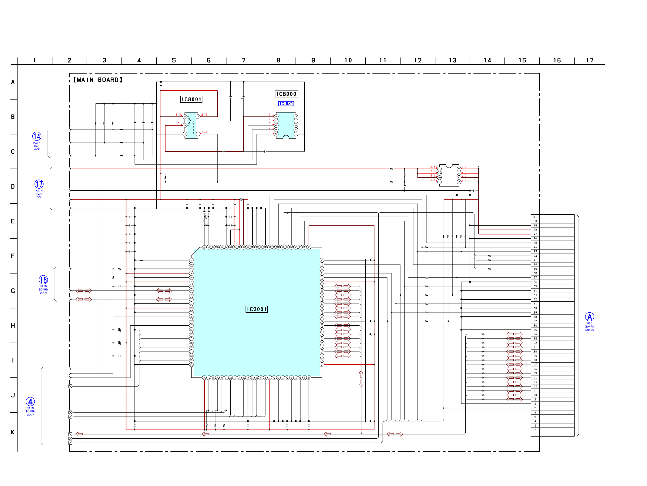
NW-HD1
5-10. SCHEMATIC DIAGRAM – MAIN Section (5/7) –
(5/7)
1
1
R8008
220k
220k
(Page 25)
(Page 28)
(Page 27)
(Page 22)
AD_GSEN_X
AD_GSEN_Y
AD_GSEN_Z
3.3V_HDD
GND_HDD
XGSEN_PWR_CTL
XURESET
USB_CNT
HDD_CNT
XUSLEEP
DATA+
DATA-
220k
R8005
R8006
R8007
3.3V
GND
VBUS
U_A
U_D
H_D
H_A
R2001
47k
R8009
47k
R8010
47k
C2005
4.7
C2006
0.1
C2007
0.1
C2008
0.1
C2009
0.1
R2004
100k
10
C2001
1
VDR2001
VDR2002
C2004
100p
C8003
C8002
C8001
R2005
5.6k
UA0
UA1
UA2
UA3
UA4
UA5
UA6
UA7
C2010 C2018 C2021 C2023
0.1 0.1 0.1 4.7
• See page 30 for IC Block Diagram. • See page 34 for IC Pin Function Description.
C8006
0.1
C8007
C8005
10
0.01
B+ SWITCH
IC8001 IC8000
SN74LVC1G66DCKR HAAM-301BS
D
D
1
R8001
470k
V
D
N
G
C2002
10p
C2011 C2012
X2001
12MHz
R2009
R1
NC
AVSS
AVDD
AVSS
AVDD
AVSS
DP
AVSS
DM
AVSS
AVDD
TSTEN
VBUS
XRESET
XSLEEP
CA0
CA1
CA2
CA3
CA4
CA5
CA6
CA7
VSS
8p 8p
0
I
O
X
X
D
S
D
C
V
X
0
S
C
U
X
C2016C2014 C2017
0.10.1 0.1
R2010
1M
C
N
D
R
X
IT
A
D
W
R
U
U
X
X
470k
R2006
6.3V
S
S
L1
S
E
V
VS
X
KS
L
C
USB CONTROLLER
∗
IC2001
S1R72003BOOA100
4
5
S
S
D
D
V
C
C
5
4
D
D
U
U
C8004
0.1
EL0
S
K
CL
6
CD
6
D
U
R8002
10
R2003
FB2001
C2013
4.7
C2015
0.1
C
S
C
D
D
D
D
S
N
N
D
D
D
D
V
V
V
V
V
P
P
X
CSP(Chip Size Package)
IT
T
A
R
0
2
1
R2008
3
D
D
D
D
C
C
C
C
3
2
1
0
D
D
D
D
U
U
U
U
470k
W
W
IN
X
X
X
Q
E
R
T
R
IN
W
U
U
X
X
470k
R2007
G-SENSOR
VDD
DZOUT
CSET
DYOUT
AOUTX
DZOUT
AOUTY
FSET
AOUTZ
GND
1
2
0
A
A
A
H
H
H
S
P
S
VS
A
D
H
X
7
D
D
CD
V
7
D
U
0
K
G
Q
S0
S1
A2
A
IA
C
C
D
D
H
X
EN
PG
T
A
D
H
H
P
XH
H
X
N
0
1
E
T
T
N
R
R
0
A
O
O
C
S
TP
TP
TIN
D
A1
D
D
AC
TR
V
H
M
IN
D
H
VSS
H
X
HIORDY
XHIOR
XHIOW
HDMARQ
VDD
HDD15
HDD0
HDD14
HDD1
HDD13
HDD2
HDD12
HDD3
VSS
HDD11
HDD4
HDD10
HDD5
HDD9
HDD6
HDD8
HDD7
XHRESET
T
VDD
U
O
1
C
S
S
S
S
S
TIN
V
O
V
Q2001
ECH8301-TL-E
B+ SWITCH
D
R2012
R2013
R2014
R2015
R2016
R2017
R2018
R2019
S
D
S
D
S
D
G
10k
4.7k
5.6k
10k
R2023
R2022
R2021
R2020
33
33
82
22
82
22
22
82
T
E
S
E
R
H
X
R2046
0
R2011
1M
R2045
C2019
0.1
HD15
HD0
HD14
HD1
HD13
HD2
HD12
HD3
C2020
0.1
HD11
C2022
HD4
10
6.3V
HD10
HD5
HD9
HD6
HD8
HD7
Q
E
R
A
C2024
0.1
M
D
H
C2026
47k
W
IO
H
X
0.1
K
Y
C
Q
D
E
A
0
R
R
IO
IO
H
H
X
X
1
R
M
S
S
T
D
C
C
IN
H
H
H
X
H
X
X
10k
R2024
10k
R2025
TP2001
C2025
0.1
CN2001
51P
33
R2026
HA2
HA0
HA1
HD15
HD0
HD14
HD1
HD13
HD2
HD12
HD3
HD11
HD4
HD10
HD5
HD9
HD6
HD8
HD7
R2029
R2030
R2031
R2032
R2033
R2034
R2035
R2036
R2037
R2038
R2039
R2040
R2041
R2042
R2043
R2044
R2027
R2028
33
33
33
33
33
33
33
33
33
33
33
33
33
33
33
33
33
33
NV
RESERVED
GND(LOGIC)
VDC(MOTOR)
VDC(LOGIC)
GND(MOTOR)
XDASP
XHCS1
XHCD0
H_A2
H_A0
XPDIAG
H_A1
XIOCS16
HINTREQ
GND
XHDMACK
CSEL
HIORDY
GND
XHIOR
GND
XHIOW
GND
HDMARQ
KEY
GND
H_D15
H_D0
H_D14
H_D1
H_D13
H_D2
H_D12
H_D3
H_D11
H_D4
H_D10
H_D5
H_D9
H_D6
H_D8
H_D7
GND
XHRESET
NC
NC
NC
NC
NC
NC
(Page 29)
NW-HD1
2626
Page 27

NW-HD1
5-11. SCHEMATIC DIAGRAM – MAIN Section (6/7) –
CN9501
LITHIUM ION
BATTERY
LIS1317HNP
4.2V 760mAh
BATT+
BATT-
(Page 28)
(CHASSIS)
(CHASSIS)
(CHASSIS)
GND
XCHG_STAT1
DC5V
GND
DATA+
DATA-
GND
VBUS
NC
DCIN6V
VBUS
GND
RTC_CE
(Page 28)
2P
2.4V
1.8V
2.0V
R9514
0
C9517
100p
CN9502
10P
USB CRADLE
CONNECTOR
VB
FB9501
FB9502
TP9504
TP9511
• See page 30 for IC Block Diagrams. • See page 19 for Waveform.
(6/7)
TP9502
IC9501
BQ24010ADRCR
OUT
IN
BAT
VCC
TS
MULTI_SO
MULTI_SCK
MULTI_SI
STAT1
PG
STAT2
ISET
.9k
470k
3
12
5
501
9
9
R
R
1
50
9
H
T
R9502
6.8k
TP9510
1
1
01
95
C
3
1
02
950
95
950
2
R
R
R
0
D
D
D
95
V
V
V
C
9504
R
D
V
BUFFER
TC7SZ126AFE
IC9502
6
7
50
9
950
R
R
D
D
V
V
VSS
CHARGE CONTROL
TP9506
REAL TIME CLOCK
IC9503
R2061K01-E2
SIO
SCLK
VDCC
C9503C9505
Q9501
NP062A300AS0
CHARGE CONTROL
CE
VSS
VCC
VSB
0.10.1
CIN
OSCOUT
OSCIN
VDD
C9508
R9505
2k
-1 -2
0.1
INTR
R9504
TP9513
S9501
BUILT-IN BATTERY
ON
AUTO SELECT
100k
C9511
1
R9503
4.7k
R9509
k
0
47
07
5
9
R
2SK354700LS0
INVERTER
S
470
Q9502
k
70
4
6
50
9
R
POWER SWITCH
IC9504
TPS2113PWR
STAT
EN
VSES
ILIM
IN1
OUT
IN2
GND
R9513
470k
R9515
D9501
CUS01(TE85R)
0
C9512
C9513
OFF
0.1
0.1
C9514
C9515
22
10V
22
10V
XCHG_PG
XCHG_STAT2
XCHG_STAT1
MULTI_SIO
DATA+
DATA-
VBUS
(Page 25)
(Page 26)
X9501
32KHz
C9510
2p
NW-HD1
C9504
.1
0
0.1
0.1
9
7
06
50
50
9
95
9
C
C
0.1
C
2727
Page 28

NW-HD1
5-12. SCHEMATIC DIAGRAM – MAIN Section (7/7) –
(7/7)
XCHG_PG
BATT_MON_CTL
PWR_FFCLR
PWR_SLEEP
PWR_CLK
PWR_STRB
RTC_CE
XRST
R9003
1M
10 16V
C9003
0.1
C9002
L9001
D9001
100µH
MA2SD32
C9005
0.22
R9006
R9004
100
1M
(Page 25)
BATT_MON_CTL
PWR_FFCLR
PWR_SLEEP
PWR_CLK
PWR_STRB
MULTI_SIO
XRST
RTC_CE
AD_BATT
• See page 30 for IC Block Diagrams. • See page 19 for Waveform.
Y
R
Y
E
L
E
K
C
K
C
F
_
F
T
M
_
E
R
R
S
_
W
D
P
A
C9009
C9012
C9013
100
1
L9002
220µH
1
1
D
D
N
N
G
G
P
P
T2
T2
S
S
R
R
X
C
0.1
6.3V
TP9001
R9016
150k
R9014
10k
R9015
1
1
1
L1
L1
O
V
2
2
D
D
N
N
G
G
P
L2
P
C
V
CO
V
POWER CONTROL
SC901584EPR2
2
O
2
V
L
TB
S
V
IC9002
2
O
C
V
B
C
K1
VB
V
M
L
H
W
R
X
V
T
Q
2
2
_
_
2
W
W
C
CIN
D
V
D
V
100k
TP9004
R9031
2
R
K4
K3
K
L
W
W
W
X
X
X
FFC
SLEEP
CLK
SEQSEL
WDT
SCK
STRB
DATA
VREF
GND
REGI1
REGO1
REGC1
REGI2
REGO2
REG2G
N
REGC2
O
3
3
C
O
I3
TE
G
G
U
E
E
EG
M
R
R
R
R9005
C9004
C9007
C9006
10
0.1
6.3V
D9002
MA2SD32
R9007
220k
100
0.22
C9001
0.1
XRST1
CRST1
XRSTIADJ
OTC1
RF1
INM1
CTL
VG
LG
PGND3
VB
VGSEL2
VGSEL1
INM2
RF2
DTC2
S
U
B
V
1.2V
1.8V
3.3V
GND
1.2V
1.8V
3.3V
GND
(Page 22)
VB
VSTBY
2.4V
1.5V
R9018
TP9013
470k
R9000
47k
Q9003
TP9006
UNR32A300LS0
INVERTER
R9019
10k
R9020 R9023
27k 36k
C9015
C9020
C9022
1
C9026
PWR_SLEEP
PWR_CLK
2.2
MULTI_SCK
PWR_STRB
MULTI_SO
0.01
1
R9038
10k
0
SWITCHING REGULATOR
IC9003
TPS62200DBVR
SW
VI
GND
EN
L9005
10µH
R9009 C9032
FB
470k 33p
R9030
150k
R9036 C9027
22k 100p
TP9007
6.3V
10
C9028
1.8V
2.0V
1.8V
3.3V
GND
1.2V
3.3V
3.3V_A
VSTBY
GND
1.2V
1.8V
3.3V
VSTBY
GND
1.5V
1.8V
3.3V
GND
1.2V
3.3V
3.3V_A
VSTBY
GND
1.2V
1.8V
3.3V
VSTBY
GND
(Page 23)
(Page 24)
(Page 25)
(Page 27)
(Page 24)
(Page 22)
RTC_CE
AD_RMCKEY
SET_KEY
D33_MODE
C9029
1
3.3V
3.3V_HDD
GND
GND_HDD
1.8V
2.0V
2.4V
3.3V
3.3V_HDD
GND
GND_HDD
1.8V
2.0V
2.4V
(Page 26)
(Page 27)
GND_HDD
3.3V_HDD
3.3V_A
1.5V
1.2V
GND
3.3V
TP9003
R9511
470k
BATT_MON_CTL
Q9503
UNR32A300LS0
XRST
RTC_CE
AD_RMCKEY
SET_KEY
VBUS
R9040 R9041
470k 1M
R9027
470k
BUFFER BUFFER
VBUS
VB
GND
Q9001,9503
-1 -2 -1 -2
BATTERY
MONITOR
SWITCH
S
Q9001
2SJ347-TE85L
R9029
22k
R9001
10k
R9002
C9008
0.22
22k
R9037
470k
Q9002Q9004
NP0A50100AS0NP0A50100AS0
D9003
MA2SD32
L9003
220µH
6.3V
TP9002
C9014C9010
2200p
C9030
10
6.3V
D9005R9013R9008
MA2SD321M470k
C9024
1000p
R9012
2.2
L9004
22
4.7µH
R9021
2k
R9022
36k
DC/DC CONVERTER
IC9001
LTC3441EDE
XSHDN
/SS
GND
PGND
SW1
SW2
PGND
C9023
1
R9024
36k
Z9004
Z9001
TP9009
Z9002
TP9008
C9031
C9025
1
C9037
1000p
FB9001
220p
C9036
C9019
47
1
6.3V
C9021
10p
R9028 R9035
3.3M 2.2M
R9033
FB
VC
VIN
PVIN
VOUT
MD/
SYNC
R9010 C9017
15k 220p
C9011 R9032 C9018 C9016
10 200k 22 22
R9034
R9011
2.2k
18k
330k
NW-HD1
2828
Page 29

NW-HD1
5-13. PRINTED WIRING BOARD – HDD Section –
1 2 3 4 5
A
HDD BOARD
44
43
(COMPONENT SIDE)
B
HDD BOARD
(CONDUCTOR SIDE)
51
50
C
CN101
MAIN BOARD
HARD DISK
DRIVE UNIT
CN100
A
CN2001
(Page 20)
:Uses unleaded solder.
1
2
2
1
1-862-778-
1-862-778-
(11)
11
(11)
5-14. SCHEMATIC DIAGRAM – HDD Section –
CN100
NV
RESERVED
GND(LOGIC)
VDC(MOTOR)
11
(Page 26)
VDC(LOGIC)
GND(MOTOR)
XDASP
XHCS1
XHCD0
H_A2
H_A0
XPDIAG
H_A1
XIOCS16
HINTREQ
GND
XHDMACK
CSEL
HIORDY
GND
XHIOR
GND
XHIOW
GND
HDMARQ
KEY
GND
H_D15
H_D0
H_D14
H_D1
H_D13
H_D2
H_D12
H_D3
H_D11
H_D4
H_D10
H_D5
H_D9
H_D6
H_D8
H_D7
GND
XHRESET
NC
NC
NC
NC
NC
NC
51P
CN101
44P
RESERVED
GND(LOGIC)
VDC(MOTOR)
VDC(LOGIC)
GND(MOTOR)
XDASP
XHCS1
XHCD0
H_A2
H_A0
XPDIAG
H_A1
XIOCS16
HINTREQ
GND
XHDMACK
CSEL
HIORDY
GND
XHIOR
GND
XHIOW
GND
HDMARQ
KEY
GND
H_D15
H_D0
H_D14
H_D1
H_D13
H_D2
H_D12
H_D3
H_D11
H_D4
H_D10
H_D5
H_D9
H_D6
H_D8
H_D7
GND
XHRESET
HARD DISK
DRIVE
UNIT
NW-HD1
2929
Page 30

NW-HD1
• IC Block Diagrams
– MAIN Board –
IC3001 CXR710160-211GH
TRST
TDO
TMS
VDIO3
LRCKI
BCKI
VDIOCD0
PCMDI
DVDD4
TEST8
TEST7
DVDD0
DVSS0
VDIO0
VDIOCD1
PF4/XRDE
PI3/BCKO
PI2/LRCKO
PI0/PCMDO
EVA
64 63 62 61 60 59 58 57 56 55 5354 52 51 50 49
1
2
3
4
5
6
7
8
9
10
11
12
13
14
15
16
TDI
TCK
TEST0
DVSS1
DVDD3
TEST2
TEST1
DAC
INTERFACE
CD-ROM
INTERFACE
EEPROM SERIAL
INTERFACE
MAGIC GATE
CORE
TEST3
TEST4
TEST5
TEST6
VDIO2
8-BIT TIMER (CH7)
8-BIT TIMER (CH6)
8-BIT TIMER (CH5)
8-BIT TIMER (CH4)
8-BIT TIMER (CH3)
DMAC (CH3)
DMAC (CH2)
WATCHDOG
TIMER
PRESCALLER/
TIME BASE TIMER
RAM
160K BYTES
RAM
512K BYTES
UART (CH0)
UART (CH1)
8-BIT TIMER/COUNTER (CH2)
8-BIT TIMER (CH1)
8-BIT TIMER/COUNTER (CH0)
8
INTERRUPT CONTROLLER
2
2
SERIAL INTERFACE
(CH0)
RAM
DMAC (CH1)
DMAC (CH0)
CLOCK GENERATOR/
SYSTEM CONTROLLER
HUFFMAN HW
VIRTUAL ENGINE
CORE
ARM77TDMI
CPU CORE
PE3/RxD148
PE2/TxD147
PE1/RxD046
PE0/TxD045
DVSS2
44
43
DVDD2
42
PC3/SCS0
41
PC2/SI0
40
PC1/SO0
39
VDIOCD2
38
PC0/SCK0
37
PF3/T3
36
PF2/EC2/INT4
35
PF1/T1
34
PF0/EC0/INT3
33
RST
IC4301 AN17020A-VB
MUTING
CTRL
1516 1314
MUTING
1
CH1 IN
2
GND
3
CH2 IN
VREF
4
VCC 1HV
REF1
5
RF
IC8000 HAAM-301BS
Z OUT (A)9Y OUT (A)8X OUT (A)7C SET6VCC
10
DUTY CYCLE
MODULATOR
1
2
3
4
GND
F SET
Z OUT (D)
Y OUT (D)5X OUT (D)
6
S/H
S/H
S/H
VCC1
BEEP
BEEP
−
+
HP/LINE
SWITCH
+
−
REF2
VCC 2HV
AMPLIFIER
DEMULTI-PLEXER
EEPROM
CH1 SENS
HEADPHONE AMP
HEADPHONE AMP
87
VCC2
MULTI-PLEXER
LINE AMP
LINE AMP
X SENSOR
Y SENSOR
Z SENSOR
12
11
10
9
CH1 OUT
PGND
CH2 OUT
CH2 SENS
IC5001 SM8142BD-G-EL
LDR
CHV
7
6
HIGH VOLTAGE
SWITCHING CIRCUIT
DIVIDING
OSCILLATOR
FOR
OUT1
CIRCUIT
3
ENA
8
DIVIDING
CIRCUIT
BOOSTING VOLTAGE AND EL DRIVING
1
2
VSS
OSC
OUT2
5
4
VDD
NW-HD1
17 18 19 20 21 22 23 24 25 26
KDI
KCLK
KCS
VDIO1
KDO
KRB
DVSS3
DVDD1
AVDPLL
AVSPLL
27 28 29
AVDMO
AVSOSC
30
XTAL
EXTAL
31 32
XIN
OSSEL
3030
Page 31

IC9001 LTC3441EDE#TR
1
SHDN/SS
GND
PGND
INTERNAL
2
3
SUPPLY
CURRENT
LIMIT
VCC
2.4V
SWB
4A
UVLO
AVERAGE
CURRENT
3.2A
SWA
LIMIT
PWM
LOGIC
AND
OUTPUT
PHASING
REVERSE CURRENT
GATE DRIVERS
AND
ANTICTOSS
CONDUCTION
PWM
COMPARATORS
THERMAL
SHUTDOWN
LIMIT
SWD
SWC
SHUTDOWN
–0.8A
EEEOR
AMP
1.22V
NW-HD1
FB
12
11
VC
VIN
10
PVIN4SW1 9
8
VOUT
5SW2
PGND
6
IC9003 TPS62200DBVR
VI 1
UNDERVOLTAGE
LOCKOUT
BIAS SUPPLY
V
I
V (COMP)
SAWTOOTH
GENERATOR
SOFT START
OSCILLATOR
COMPARATOR
1 MHz
1MHz
OSC
SYNC
CURRENT LIMIT
COMPARATOR
SKIP COMPARATOR
CONTROL
LIGIC
SLEEP
SHOOT-THROUGH
BURST MODE
OPERATION
CONTROL
5µs DELAY1/2
DRIVER
LOGIC
REF
REF
7
MODE/SYNC
SW5
GND 2
EN 3
GM
COMPENSATION
LOAD COMPARATOR
FB4
VREF=0.5V
31
Page 32

NW-HD1
IC9002 SC901584EPR2
RESET 2
VREF
REF2
DC/DC CONVERTER
REF1
REF1
VC
VREF
PGND116PGND1
XRST233CRST2
34
REF2
VREF
STEP UP
RST1
RST2
VB
RESET 1
32 DTC2
31 RF2
30 INM2
29 VGSEL1
28 VGSEL2
27 VB
26 PGND3
25 LG
24 VG
23 C1L
22 INM1
21 RF1
20 DTC1
19 XRST1ADJ
18 CRST1
17 XRST1
REGI3
46
47
48
SERIAL
PASS
REGULATOR 3
49REGC2
50REG2G
51REGO2
52REGI2
53REGC1
54REGO1
55REGI1
56GND
57VREF
58DATA
59STRB
60CLK
61WDT
62SEQSEL
63CLK
64SLEEP
SERIAL
PASS
REGULATOR 2
SERIAL
PASS
REGULATOR 1
VG SELECT, VG DUTY
CONTROL
1
2
XWK43XWK34XWK25XWK1
FFCLR
CLK
45
FFCLR
6
VRMC
43
44
MUTING
BUFFER
SEQSEL
BANDGAP
REFERENCE
REF1
REF2
REF DAC
LVB
DRIVER
7
LVB
RST1
RST2
VREF
8
REF3
HVB
VC2
RST2
REF4
42
REF5
9
VTSB
41
POWER
SWITCH 2
MUTE ON
VREF0
RST1
VC
VC
10
40
VCVREF0
VC1
POWER
SWITCH 1
11
VCO1
UP-DOWN
DRIVER
RST2
VCO2
VCIN
VC2
DW 2T
DW 2B
MUTEON
REGC3
REGO3
39
STEP
PWM
L237L238VO2
36
VC2
START UP
PWM
STEP
UP-DOWN
DRIVER
12
VO1
VC
VREF
13L114L115
PGND235PGND2
IC9503 R2061K01-E2
CE
SIO 1
SCLK 2
/VDCC 3
12
LEVEL
SHIFTER
4
VSB
11
DELAY
32
VSS
REAL
TIME
CLOCK
VOLTAGE
DETECTOR
CIN
10
VOLTAGE
REFERENCE
5
6
VCC
VDD
BATTERY
VOLTAGE
MONITOR
9 /INTR
8 OSCOUT
7 OSCIN
Page 33

IC9501 BQ24010ADRCR
NW-HD1
2
VCC VCC
STAT1 3
STAT2 4
VSS 5
VO (REG)
VI (BAT)
VO (REG)
VI (BAT)
VI (SET)
VI (BAT)
VI (SET)
V (ISET)
VSET
DEGLITCH
DEGLITCH
DEGLITCH
CHARGE
CONTROL,
TIMER,
AND
DISPLY
LOGIC
VO (REG)
DEGLITCH
THERMAL
SHUTDOWN
REFERENCE
AND BIAS
VI (BAT)
V (SLP)
VCC
VCC
VI (BAT)
OUT10IN 1
BAT9
TS8
PG7
ISET6
IC9504 TPS2113PWR
1µA
STAT 1
EN
2
VSNS 3
0.8V
CHARGE
PUMP
ILIM 4
0.5V
THERMAL
SENSE
CONTROL
LOGIC
VDD
ULVO
IN2
ULVO
IN1
ULVO
CROSS-CONDUCTION
DETECTOR
INTERNAL
VDD
IN18
OUT7
IN26
GND
5
33
Page 34

NW-HD1
• IC Pin Function Description
MAIN BOARD IC1003 CXR704060-201GA (SYSTEM CONTROLLER, D/A CONVERTER)
Pin No. Pin Name I/O Description
1 VDIO0 —
PM4/A12 to
2 to 10
PM7/A15,
PN0/A16 to
PN4/A20
Power supply terminal (+1.8V) (for I/O interface)
O
Address signal output to the flash memory and multi interface
11 to 13
14 DVSS7 —
15 to 22 FAD0 to FAD7 I/O
23 FCLE O
24 FALE O
25 VDIODF —
26 FWE O
27 PRE O
28 FWP O
29 FCE0 O
30 FRB0 I
31 FCE1 O
32 FRB1 I
33 PP0/RP O
34 PP1/RB O
35 DVDD0 —
36 DVSS1 —
37 VDIO1 —
38 to 53
54 PA0/PWM O
55 PA1/SDA O
56 PA2/SCL O
57 PC0/SCK0 I
58 PC1/SO0 O
59 PC2/SI0 I
60 PC3/SCS0 O
61 DVSS2 —
62 VDIO2 —
63 KDI O
64 KRB O
65 KCLK O
66 KCS O
67 KDO O
68 TEST4 I
69 PE0/TXD0 O
70 PE1/RXD0 I
71 PE2/TXD1 O
PN5/A21 to
PN7/A23
PO0/D0 to PO7/D7,
PB0/D8 to PB7/D15
O
I/O
Address signal output to the multi interface
Ground terminal
Not used
Not used
Not used
Power supply terminal (for NAND flash memory interface) Not used
Not used
Not used
Not used
Not used
Not used
Not used
Not used
Wake up signal output to the sub system controller
Communication request signal output to the sub system controller
Power supply terminal (+1.2V) (for core)
Ground terminal
Power supply terminal (+1.8V) (for I/O interface)
Two-way data bus with the flash memory and multi interface
Not used
Not used
Not used
Serial clock signal input from the sub system controller
Serial data output to the sub system controller
Serial data input from the sub system controller
Chip select signal output to the sub system controller
Ground terminal
Power supply terminal (+1.8V) (for I/O interface)
Not used
Not used
Not used
Not used
Not used
Input terminal for the test mode setting
Data output terminal Not used
Data input terminal Not used
Strobe signal output to the power control
34
Page 35

Pin No. Pin Name I/O Description
72 PE3/RXD1 I
73 PE4/SCK1 O
74 PE5/SO1 O
75 PE6/SI1 I
76 PE7/SCS1 O
77 XOUT/CKO O
78 DVDD1 —
79 DVSS3 —
80 VDIO3 —
81 PF0/EC0/INT3 I
82 PF1/T1 O
83 PF2/EC2/INT4 I
84 PF3/T3 O
85 PF4/BEEP O
86 PG0/DACK0 I
87
88
89
90 to 93
94 TACK O
95 EVA I
96 AVSAD —
97 AVDAD —
98 AN0 I
99 AN1 I
100 AN2 I
101 AN3 I
102 AN4 I
103, 104 AN5, AN6/INT8 I
105 AN7/INT9 I
106 RST I
107 RAMBK I
108 VDBK —
109 TDI I
110 TMS I
111 TCK I
112 TRST I
113 TDO O
114 VDIOJT —
115 DVDD2 —
116 DVSS4 —
117 VDIO4 —
118 PD0/CONNECT O
119 PD1/XVDATA O
PG1/DREQ0/INT5
PG2/DACK1/INT6
PG3/DREQ1/INT7
TEST2, TEST3,
TEST0, TEST1
Data input terminal Not used
Serial clock signal output to the power control and real time clock
Serial data output to the power control and real time clock
Serial data input from the real time clock
Chip enable signal output to the real time clock
Clock signal (176 kHz) output to the multi interface
Power supply terminal (+1.2V) (for core)
Ground terminal
Power supply terminal (+1.8V) (for I/O interface)
Interrupt request signal input from the sub system controller
Shut down signal output to the DC/DC converter
Interrupt request signal input from the multi interface
Clock signal (176 kHz) output to the power control
Beep signal output to the headphone amplifier
Ready/busy selection signal input from the flash memory “L”: busy, “H”: ready
I
Interrupt request signal input from the sub system controller
I
Interrupt request signal input from the multi interface
I
Interrupt request signal input from the multi interface
I
Input terminal for the test mode setting
Bus response signal output terminal Not used
EVA mode selection signal input terminal Not used
Ground terminal (for A/D converter)
Power supply terminal (+2.4V) (for A/D converter)
Battery voltage monitor input terminal (A/D input)
Not used
Acceleration detection signal of X shaft direction input from the acceleration sensor
Acceleration detection signal of Y shaft direction input from the acceleration sensor
Acceleration detection signal of Z shaft direction input from the acceleration sensor
Set key input terminal (A/D input)
Remote commander key input terminal (A/D input)
Reset signal input from the power control
RAM back up control signal input terminal Not used
Power supply terminal (+1.2V) (for RAM back up)
Data input terminal (for JTAG) Not used
Test mode control signal input terminal (for JTAG) Not used
Clock signal input terminal (for JTAG) Not used
Reset signal input terminal (for JTAG) Not used
Data output terminal (for JTAG) Not used
Power supply terminal (+1.8V) (for JTAG)
Power supply terminal (+1.2V) (for core)
Ground terminal
Power supply terminal (+1.8V) (for I/O interface)
Test terminal for debug Not used
Test terminal for debug Not used
NW-HD1
35
Page 36

NW-HD1
Pin No. Pin Name I/O Description
120 PD2/DPLS O
121 PD3/DMNS O
122 PD4/TXDPLS O
123 PD5/TXDMNS O
124 PD6/TXENL O
125 PD7/SUSPEND O
126 VBUS I
127 VDIOUS —
128 UDM I/O
129 UDP I/O
130 TRON O
131 AVSDA —
132 VREFER O
133 AOUTR O
134 AOUTL O
135 VREFL O
136 AVDDA —
137 XTAL O
138 EXTAL I
139 AVDMO —
140 AVSOSC —
141 TX O
142 ETX I
143 AVDUO —
144 AVSPLL —
145 AVDPLL —
146 PQ0/PGMTR0 O
147 PQ1/PGMTR1 O
148 PQ2/PGMTR2 I
149 PQ3/PGMTR3 I
150 PQ4 I
151 PQ5 O
152 PQ6 O
153 PQ7 O
154 DVSS8 —
155 VDIO7 —
156 PR0 O
157 to 161 PR1 to PR5 —
162 PR6 O
163 PR7 O
164 DVSS9 —
165 VDIOMS —
166 MSDIO I/O
167 MSBS O
168 MSSCLK O
Test terminal for debug Not used
Test terminal for debug Not used
Test terminal for debug Not used
Test terminal for debug Not used
Test terminal for debug Not used
Test terminal for debug Not used
Not used
Power supply terminal (for USB transceiver) Not used
Not used
Not used
Not used
Ground terminal (for internal D/A converter)
Reference voltage output terminal (R-ch)
Analog audio signal output to the headphone amplifier (R-ch)
Analog audio signal output to the headphone amplifier (L-ch)
Reference voltage output terminal (L-ch)
Power supply terminal (+2.4V) (for internal D/A converter)
Main system clock output terminal (22.5792 MHz)
Main system clock input terminal (22.5792 MHz)
Power supply terminal (+2.4V) (for main system clock oscillator)
Ground terminal (for main and sub system clock oscillator)
Sub system clock output terminal (16 MHz)
Sub system clock input terminal (16 MHz)
Power supply terminal (+2.4V) (for sub system clock oscillator)
Ground terminal (for PLL)
Power supply terminal (+3.3V) (for PLL analog system)
Sleep signal output to the power control
Starting factor clear signal output to the power control
Charge progress signal input from the charge control
Charge completion signal input from the charge control
Power good signal input from the power switch
Sleep signal output to the multi interface
Reset signal output to the sub system controller
Reset signal output to the multi interface
Ground terminal
Power supply terminal (+1.8V) (for I/O interface)
Battery voltage monitor on/off control signal output terminal
Not used
Headphone/line selection signal output to the headphone amplifier
Muting on/off control signal output to the headphone amplifier
Ground terminal
Power supply terminal (+3.3V) (for memory stick interface) Not used
Two-way data bus with the memory stick interface Not used
Bus state signal output to the memory stick interface Not used
Clock signal output to the memory stick interface Not used
36
Page 37

Pin No. Pin Name I/O Description
169 MSINS I
170 P17 I
171 P10/DADT O
172 P11/ADDT I
173 P12/LRCK I
174 P13/BCK I
175 P14/FS256 O
176 P15/MUTFGL O
177 P15/MUTFGR O
178 DVDD3 —
179 DVSS5 —
180 VDIO5 —
181 PJ0/WAIT I
182 PJ1/RE O
183 PJ2/LWR/LB O
184 PJ3/UWR/UB O
185 PJ4/WE O
186 PK0/CS0 O
187 PK1/CS1 O
188 PK2/XBOOT I
189 PK3/MS_SIO I
190 PK4 I
191 PK5/CS5 I
192 PK6/CS6 I
193 PK7/CS7 I
194 DVSS6 —
195 VDIO6 —
196 to 207
208 DVSS6 —
PL0/A0 to PL7/A7,
PM0/A8 to PM3/A11
Card detection signal input from the memory stick interface Not used
HOLD key detection signal input terminal “L”: hold
Audio data input from the memory stick interface Not used
Audio data input from the sub system controller
L/R sampling clock signal input from the sub system controller
Bit clock signal input from the sub system controller
Clock signal (11.2896 MHz) output to the multi interface
Not used
Not used
Power supply terminal (+1.2V) (for core)
Ground terminal
Power supply terminal (+1.8V) (for I/O interface)
Wait signal input from the multi interface
Read signal output to the multi interface
Write strobe signal output to the multi interface (lower byte)
Write strobe signal output to the multi interface (upper byte)
Write signal output to the multi interface
Chip select signal output to the multi interface
Chip select signal output terminal Not used
Boot mode selection signal input terminal Not used
Boot mode selection signal input terminal Not used
Not used
Chip select signal input from the multi interface
Chip select signal input from the multi interface
Chip select signal input from the multi interface
Ground terminal
Power supply terminal (+1.8V) (for I/O interface)
O
Address signal output to the flash memry and mullet interface
Ground terminal
NW-HD1
37
Page 38

NW-HD1
MAIN BOARD IC2001 1S1R72003BOOA100 (USB CONTROLLER)
Pin No. Pin Name I/O Description
1R1I/O
2 N.C. —
3AVSS—
4 AVDD —
5AVSS—
6 AVDD —
7AVSS—
8DP
9AVSS—
10 DM I/O USB data (–) input/output terminal
11 AVSS —
12 AVDD —
13 TSTEN I
14 VBUS I
15 XRESET I
16 XSLEEP I
17 to 24 CA0 to CA7 I
25 VSS —
26 VDD —
27 XCS I
28 XRD I
29 XWAIT O
30 XWR I
31 XINT O
32 to 35 CD0 to CD3 I/O
36 VSS —
37 to 40 CD4 to CD7 I/O
41 VDD —
42 ATPGEN I
43 SCANEN I
44, 45
46, 47 TIN0, TIN1 I
53 to 60 HDD4 to HDD11 I/O
62 to 69
TPORT0, TPORT1
48 VSS —
49 OSCOUT O
50 VSS —
51 VDD —
52 XHRESET I
61 VSS —
HDD0 to HDD3,
HDD12 to HDD15
70 VDD —
71 HDMARQ I
72 XHIOW O
73 XHIOR O
Internal operation setting terminal
Not used
Ground terminal (analog system)
Power supply terminal (+3.3V) (analog system)
Ground terminal (analog system)
Power supply terminal (+3.3V) (analog system)
Ground terminal (analog system)
I/O USB data (+) input/output terminal
Ground terminal (analog system)
Ground terminal (analog system)
Power supply terminal (+3.3V) (analog system)
Input terminal for the test mode setting
USB bus detection signal input terminal
Reset signal input from the multi interface
Sleep signal input from the multi interface
Address signal input from the multi interface
Ground terminal (logic system)
Power supply terminal (+3.3V) (logic system)
Chip select signal input from the multi interface
Read signal input from the multi interface
Wait signal output to the multi interface
Write signal input from the multi interface
Interrupt request signal output to the multi interface
Two-way data bus with the multi interface and liquid crystal display unit
Ground terminal (logic system)
Two-way data bus with the multi interface and liquid crystal display unit
Power supply terminal (+3.3V) (logic system)
Input terminal for the test mode setting
Input terminal for the test mode setting
I/O
Input/output terminal for the test mode setting
Input terminal for the test mode setting
Ground terminal (logic system)
Clock signal output terminal Not used
Ground terminal (logic system)
Power supply terminal (+3.3V) (logic system)
Reset signal input terminal Not used
Two-way data bus with the multi interface and hard disk drive unit
Ground terminal (logic system)
I/O
Two-way data bus with the multi interface and hard disk drive unit
Power supply terminal (+3.3V) (logic system)
DMA request signal input from the hard disk drive unit
Write signal output to the hard disk drive unit
Read signal output to the hard disk drive unit
38
Page 39

Pin No. Pin Name I/O Description
74 HIORDY I
75 VSS —
76 VDD —
77 XHDMACK O
78 HINTRQ I
79 HA1 O
80 XHPDIAG I
81, 82 HA0, HA2 O
83, 84 HCS0, HCS1 O
85 XHDASP I
86 VSS —
87, 88
89 VSS —
90 XVSS —
91 XVDD —
92 VDD —
93 PVDD —
94 VDD —
95 PVSS —
96 to 98 NC —
99 XI I
100 XO O
CLKSEL0,
CLKSEL1
Wait signal input from the hard disk drive unit
Ground terminal (logic system)
Power supply terminal (+3.3V) (logic system)
DMA acknowledge signal output to the hard disk drive unit
Interrupt request signal input from the hard disk drive unit
Address signal output to the multi interface and hard disk drive unit
Diagnosis sequence compression signal input from the hard disk drive unit
Address signal output to the multi interface and hard disk drive unit
Chip select signal output to the hard disk drive unit
Drive valid signal and slave drive detection signal input from the hard disk drive unit
Ground terminal (logic system)
I
Input terminal for oscillation frequency setting Fixed at 12 MHz in this set
Ground terminal (logic system)
Ground terminal (logic system)
Power supply terminal (+3.3V) (logic system)
Power supply terminal (+3.3V) (logic system)
Power supply terminal (+3.3V) (for PLL)
Power supply terminal (+3.3V) (logic system)
Ground terminal (for PLL)
Not used
Sub system clock input terminal (12MHz)
Sub system clock output terminal (12MHz)
NW-HD1
39
Page 40

NW-HD1
6
4
MAIN BOARD IC7001 CXD1616GH (MULTI INTERFACE)
Pin No. Pin Name I/O Description
1 XTAL I
2 EXTAL O
3 CLK2550A O
4 CLK2550X O
5XOSCSTP I
6 XRESET I
7 EXCLKIN I
8 to 30 A1 to A23 I
31 to 46 D0 to D15 I/O
47 to 49 XCS1 to XCS3 I
50 XRD I
51 XWR I
52 XLB I
53 XUB I
54 XWAIT I
55, 56 NC —
57 XINTREQG O
58 XINTREQH O
59 XINTREQU O
60 to 72 SA0 to SA12 O
73, 74 BA0, BA1 O
75 to 90 SD0 to SD15 I/O
91 XSCS O
92 XRAS O
93 XCAS O
94 XSWE O
95 LDQM O
96 UDQM O
97 SDCLK O
98 SDCKE O
99 UA0 O
100 to 10
107 to 11
115 XUCS0 O
116 XUCS1 O
117 XURD O
118 XUWR O
119 XUWAIT I
120 XUINTREQ I
121 to 123 HA0 to HA2 I
124 to 139 HD0 to HD15 I/O
140, 141 XHCS0, XHCS1 O
142 XHIOR O
143 XHIOW O
UA1 to UA7 O
UD0 to UD7 I/O
Sub system clock input terminal Not used
Sub system clock output terminal Not used
Clock signal (22.5792 MHz) output to the sub system controller
Clock signal (22.5792 MHz) inversion output to the sub system controller
Oscillation stop signal input terminal Not used
Reset signal input from the main system controller
Clock signal (176 kHz) input from the main system controller
Address signal input from the main system controller
Two-way data bus with the main system controller and flash memory
Chip select signal input from the main system controller
Read signal input from the main system controller
Write signal input from the main system controller
Write strobe signal input from the main system controller (lower byte)
Write strobe signal input from the main system controller (upper byte)
Wait signal input from the main system controller
Not used
Interrupt request signal output to the main system controller
Interrupt request signal output to the main system controller
Interrupt request signal output to the main system controller
Address signal output to the SD-RAM
Bank selection address signal output to the SD-RAM
Two-way data bus with the SD-RAM
Chip select signal output to the SD-RAM
Row address strobe signal output to the SD-RAM
Column address strobe signal output to the SD-RAM
Write enable signal output to the SD-RAM
I/O mask signal output to the SD-RAM (lower byte)
I/O mask signal output to the SD-RAM (upper byte)
Clock signal output to the SD-RAM
Clock enable signal output to the SD-RAM
Address signal output to the USB controller and liquid crystal display unit
Address signal output to the USB controller
Two-way data bus with the USB controller and liquid crystal display unit
Chip select signal output to the USB controller
Chip select signal output to the liquid crystal display unit
Read signal output to the USB controller and liquid crystal display unit
Write signal output to the USB controller and liquid crystal display unit
Wait signal output to the USB controller
Interrupt request signal output to the USB controller
Address signal input from the USB controller
Two-way data bus with the USB controller and hard disk drive unit
Chip select signal output to the hard disk drive unit
Read signal output to the hard disk drive unit
Write signal output to the hard disk drive unit
40
Page 41

Pin No. Pin Name I/O Description
2
0
0
6
144 HIORDY I
145 XHDMACK O
146 HDMARQ I
147 HINTREQ I
148 XHRESET O
149 LRCK O
150 BCK O
151 DATA O
152 XRDE O
153 FS256 I
154 DTCK I/O
155 URESET O
156 USLEEP O
157 HDD_PWR_CTL O
GSEN_PWR_CTL
158
159 BACKLIT_PWR O
160 D33_MODE O
161 RESET_LCD O
162 XEL_PWR_CTL I/O
163 GPIO8 I/O
164 SYNCMODE I
165 TDI I
166 TMS I
167 TCK I
168 TRST I
169 TDO O
170 to 17
175 to 19
191 to 20
201 to 20
207 to 223 GND —
224 to 228 NC —
TEST0 to TEST2 I
173 XICKSTP I
174 NC —
VDE33 —
VDE33 —
VDE33 —
Wait signal input from the hard disk drive unit
DMA acknowledge signal output to the hard disk drive unit
DMA request signal input from the hard disk drive unit
Interrupt request signal input from the hard disk drive unit
Reset signal output to the hard disk drive unit
L/R sampling clock signal output to the sub system controller
Bit clock signal output to the sub system controller
Transmission data output to the sub system controller
Transmission enabling signal output to the sub system controller
Clock signal (11.2896 MHz) input from the main system controller
Two-way TSB communication data bus with the remote commander
Reset signal output to the USB controller
Sleep signal output to the USB controller
Power supply on/off control signal output terminal for hard disk drive unit Not used
O
Power supply on/off control signal output terminal for acceleration sensor
Power supply on/off control signal output terminal for liquid crystal display back light
Power supply on/off control signal output to the DC/DC converter for +3.3V power supply
Reset signal output to the liquid crystal display unit
Not used
Not used
Sync/non-sync mode selection signal input terminal Not used
Data input terminal (for JTAG) Not used
Test mode control signal input terminal (for JTAG) Not used
Clock signal input terminal (for JTAG) Not used
Reset signal input terminal (for JTAG) Not used
Data output terminal (for JTAG) Not used
Input terminal for the test mode setting
Sleep signal input from the main system controller
Not used
Power supply terminal (+1.2V)
Power supply terminal (+1.8V)
Power supply terminal (+3.3V)
Ground terminal
Not used
NW-HD1
41
Page 42

NW-HD1
Ver 1.1
SECTION 6
EXPLODED VIEW
NOTE:
• -XX and -X mean standardized parts, so they
may have some difference from the original
one.
• Color Indication of Appearance Parts
Example:
KNOB, BALANCE (WHITE) . . . (RED)
↑↑
Parts Color Cabinet's Color
1
2
3
5
32
6
31
• Items marked “*” are not stocked since they
are seldom required for routine service. Some
delay should be anticipated when ordering
these items.
• The mechanical parts with no reference
number in the exploded views are not supplied.
• Accessories are given in the last of the
electrical parts list.
2
9
20 21
35
24
4
30
27
26
29
33
3
10
11
14
13
12
19
25
28
7
8
Ref. No. Part No. Description Remark
1 X-2022-998-1 CABINET (UPPER) (S) SUB ASSY (SILVER)
(France, UK)
1 X-2022-999-1 CABINET (UPPER) (B) SUB ASSY (BLACK)
1 X-2023-000-1 CABINET (UPPER) (S) SUB ASSY (SILVER)
1 X-2023-001-1 CABINET (UPPER) (B) SUB ASSY (BLACK)
2 3-234-449-09 SCREW (M1.4) (for BLACK)
2 3-234-449-11 SCREW (M1.4) (for SILVER)
3 3-238-876-04 SCREW (M1.4), TOOTHED LOCK
4 X-2023-758-1 BATTERY BLOCK SUB ASSY (US, Canadian)
4 X-2023-759-1 BATTERY BLOCK SUB ASSY (France, UK)
5 X-2023-003-1 LCD BLOCK SUB ASSY
6 X-2023-004-1 MAIN BOARD, COMPLETE (for SERVICE)
7 1-863-393-11 FLEXIBLE BOARD
8 2-102-757-01 INSULATING (PC BOARD)
9 1-478-820-11 SWITCH UNIT (H)
10 X-2022-217-1 BRACKET (AB) ASSY
11 2-102-782-01 CABINET (LOWER) (BLACK)
11 2-102-782-11 CABINET (LOWER) (SILVER)
12 2-102-768-01 KNOB (BATT)
13 2-102-769-01 KNOB (HOLD)
(France, UK)
(US, Canadian)
(US, Canadian)
15
16 18
34
17
Ref. No. Part No. Description Remark
14 2-102-761-01 INSULATOR
15 1-478-858-11 HDD UNIT
16 A-1063-220-A HDD BOARD, COMPLETE
17 2-102-759-01 SHEET (DAMPER)
18 2-148-643-01 SHEET (SHIELD HDD)
19 2-148-885-01 SHEET (INSULATING HDD FLEXIBLE)
20 2-149-476-01 SPACER (CABINET LOWER)
21 2-149-476-11 SPACER (CABINET LOWER)
24 2-187-212-01 SHEET (BRACKET B)
25 2-178-122-01 SPACER E
26 2-178-123-01 SPACER F
27 2-178-124-02 SPACER G
28 2-178-125-01 SPACER H
29 2-178-126-01 SPACER I
30 2-178-127-02 SPACER J
31 2-178-527-01 SHEET (HP)
32 2-186-926-02 SHEET (SHIELD IC)
33 2-186-925-01 SHEET (SHIELD USB)
34 2-318-882-01 SHEET (USB HORIZONTAL)
35 2-102-781-01 ESCUTCHEON (CRADLE) (SILVER)
35 2-102-781-11 ESCUTCHEON (CRADLE) (BLACK)
42
Page 43

SECTION 7
ELECTRICAL PARTS LIST
NW-HD1
Ver 1.1
MAINHDD
NOTE:
• Due to standardization, replacements in the
parts list may be different from the parts
specified in the diagrams or the components
used on the set.
• -XX and -X mean standardized parts, so they
may have some difference from the original
one.
• RESISTORS
All resistors are in ohms.
METAL: Metal-film resistor.
METAL OXIDE: Metal oxide-film resistor.
F: nonflammable
Ref. No. Part No. Description Remark Ref. No. Part No. Description Remark
A-1063-220-A HDD BOARD, COMPLETE
********************
< CONNECTOR >
CN100 1-818-601-11 CONNECTOR, FPC (ZIF) 51P
************************************************************
X-2023-004-1 MAIN BOARD, COMPLETE (for service)
*********************
2-178-122-01 SPACER E
2-178-123-01 SPACER F
2-178-124-01 SPACER G
2-178-125-01 SPACER H
2-178-126-01 SPACER I
2-178-127-01 SPACER J
2-178-527-01 SHEET (HP)
2-186-925-01 SHEET (SHIELD USB)
2-186-926-02 SHEET (SHIELD IC)
2-318-882-01 SHEET (USB HORIZONTAL)
< CAPACITOR >
C1001 1-100-504-11 CERAMIC CHIP 0.1uF 20% 6.3V
C1002 1-100-504-11 CERAMIC CHIP 0.1uF 20% 6.3V
C1003 1-100-504-11 CERAMIC CHIP 0.1uF 20% 6.3V
C1004 1-100-504-11 CERAMIC CHIP 0.1uF 20% 6.3V
C1005 1-100-504-11 CERAMIC CHIP 0.1uF 20% 6.3V
C1006 1-100-504-11 CERAMIC CHIP 0.1uF 20% 6.3V
C1007 1-100-504-11 CERAMIC CHIP 0.1uF 20% 6.3V
C1008 1-100-504-11 CERAMIC CHIP 0.1uF 20% 6.3V
C1009 1-100-504-11 CERAMIC CHIP 0.1uF 20% 6.3V
C1010 1-100-504-11 CERAMIC CHIP 0.1uF 20% 6.3V
C1011 1-100-504-11 CERAMIC CHIP 0.1uF 20% 6.3V
C1012 1-100-504-11 CERAMIC CHIP 0.1uF 20% 6.3V
C1013 1-100-504-11 CERAMIC CHIP 0.1uF 20% 6.3V
C1014 1-128-617-11 CERAMIC CHIP 100PF 5% 25V
C1015 1-128-617-11 CERAMIC CHIP 100PF 5% 25V
C1016 1-128-617-11 CERAMIC CHIP 100PF 5% 25V
C1017 1-100-504-11 CERAMIC CHIP 0.1uF 20% 6.3V
C1018 1-100-504-11 CERAMIC CHIP 0.1uF 20% 6.3V
C1019 1-128-617-11 CERAMIC CHIP 100PF 5% 25V
C1020 1-100-504-11 CERAMIC CHIP 0.1uF 20% 6.3V
C1021 1-100-506-11 CERAMIC CHIP 1uF 20% 6.3V
C1022 1-100-504-11 CERAMIC CHIP 0.1uF 20% 6.3V
C1023 1-100-504-11 CERAMIC CHIP 0.1uF 20% 6.3V
• Items marked “*” are not stocked since they
are seldom required for routine service.
Some delay should be anticipated when
ordering these items.
• SEMICONDUCTORS
In each case, u: µ, for example:
uA... : µA... uPA... : µPA...
uPB... : µPB... uPC... : µPC...
uPD... : µPD...
• CAPACITORS
uF: µF
• COILS
uH: µH
C1024 1-100-504-11 CERAMIC CHIP 0.1uF 20% 6.3V
C1025 1-100-506-11 CERAMIC CHIP 1uF 20% 6.3V
C1026 1-128-617-11 CERAMIC CHIP 100PF 5% 25V
C1027 1-100-506-11 CERAMIC CHIP 1uF 20% 6.3V
C1028 1-100-504-11 CERAMIC CHIP 0.1uF 20% 6.3V
C1030 1-128-617-11 CERAMIC CHIP 100PF 5% 25V
C1101 1-128-617-11 CERAMIC CHIP 100PF 5% 25V
C1103 1-100-504-11 CERAMIC CHIP 0.1uF 20% 6.3V
C2001 1-165-908-11 CERAMIC CHIP 1uF 10% 10V
C2002 1-128-604-11 CERAMIC CHIP 10PF 0.5PF 25V
C2004 1-128-617-11 CERAMIC CHIP 100PF 5% 25V
C2005 1-100-507-91 CERAMIC CHIP 4.7uF 20% 6.3V
C2006 1-100-504-11 CERAMIC CHIP 0.1uF 20% 6.3V
C2007 1-100-504-11 CERAMIC CHIP 0.1uF 20% 6.3V
C2008 1-100-504-11 CERAMIC CHIP 0.1uF 20% 6.3V
C2009 1-100-504-11 CERAMIC CHIP 0.1uF 20% 6.3V
C2010 1-100-504-11 CERAMIC CHIP 0.1uF 20% 6.3V
C2011 1-127-998-11 CERAMIC CHIP 8PF 0.5PF 25V
C2012 1-127-998-11 CERAMIC CHIP 8PF 0.5PF 25V
C2013 1-100-507-91 CERAMIC CHIP 4.7uF 20% 6.3V
C2014 1-100-504-11 CERAMIC CHIP 0.1uF 20% 6.3V
C2015 1-100-504-11 CERAMIC CHIP 0.1uF 20% 6.3V
C2016 1-100-504-11 CERAMIC CHIP 0.1uF 20% 6.3V
C2017 1-100-504-11 CERAMIC CHIP 0.1uF 20% 6.3V
C2018 1-100-504-11 CERAMIC CHIP 0.1uF 20% 6.3V
C2019 1-100-504-11 CERAMIC CHIP 0.1uF 20% 6.3V
C2020 1-100-504-11 CERAMIC CHIP 0.1uF 20% 6.3V
C2021 1-100-504-11 CERAMIC CHIP 0.1uF 20% 6.3V
C2022 1-117-919-11 TANTALUM CHIP 10uF 20% 6.3V
C2023 1-100-507-91 CERAMIC CHIP 4.7uF 20% 6.3V
C2024 1-100-504-11 CERAMIC CHIP 0.1uF 20% 6.3V
C2025 1-100-504-11 CERAMIC CHIP 0.1uF 20% 6.3V
C2026 1-100-504-11 CERAMIC CHIP 0.1uF 20% 6.3V
C3001 1-100-504-11 CERAMIC CHIP 0.1uF 20% 6.3V
C3002 1-100-506-11 CERAMIC CHIP 1uF 20% 6.3V
C3003 1-128-617-11 CERAMIC CHIP 100PF 5% 25V
C3004 1-100-504-11 CERAMIC CHIP 0.1uF 20% 6.3V
C3005 1-100-506-11 CERAMIC CHIP 1uF 20% 6.3V
C3006 1-100-504-11 CERAMIC CHIP 0.1uF 20% 6.3V
C3007 1-100-504-11 CERAMIC CHIP 0.1uF 20% 6.3V
C3008 1-100-504-11 CERAMIC CHIP 0.1uF 20% 6.3V
C3009 1-100-504-11 CERAMIC CHIP 0.1uF 20% 6.3V
C3010 1-100-504-11 CERAMIC CHIP 0.1uF 20% 6.3V
The components identified by mark
0 or dotted line with mark 0 are
critical for safety.
Replace only with part number
specified.
Les composants identifiés par une
marque 0 sont critiquens pour la
sécurité.
Ne les remplacer que par une pièce
portant le numéro spécifié.
When indicating parts by reference
number, please include the board.
43
Page 44

NW-HD1
MAIN
Ref. No. Part No. Description Remark
C3011 1-100-504-11 CERAMIC CHIP 0.1uF 20% 6.3V
C3012 1-100-504-11 CERAMIC CHIP 0.1uF 20% 6.3V
C3013 1-100-506-11 CERAMIC CHIP 1uF 20% 6.3V
C3015 1-100-504-11 CERAMIC CHIP 0.1uF 20% 6.3V
C3017 1-100-504-11 CERAMIC CHIP 0.1uF 20% 6.3V
C3018 1-100-504-11 CERAMIC CHIP 0.1uF 20% 6.3V
C4101 1-100-506-11 CERAMIC CHIP 1uF 20% 6.3V
C4102 1-128-628-11 CERAMIC CHIP 0.0022uF 10% 6.3V
C4103 1-128-625-11 CERAMIC CHIP 470PF 10% 16V
C4104 1-135-868-11 TANTALUM CHIP 220uF 20% 2.5V
C4105 1-113-600-11 TANTALUM CHIP 2.2uF 20% 6.3V
C4106 1-128-632-11 CERAMIC CHIP 0.01uF 10% 6.3V
C4201 1-100-506-11 CERAMIC CHIP 1uF 20% 6.3V
C4202 1-128-628-11 CERAMIC CHIP 0.0022uF 10% 6.3V
C4203 1-128-625-11 CERAMIC CHIP 470PF 10% 16V
C4204 1-135-868-11 TANTALUM CHIP 220uF 20% 2.5V
C4205 1-113-600-11 TANTALUM CHIP 2.2uF 20% 6.3V
C4206 1-128-632-11 CERAMIC CHIP 0.01uF 10% 6.3V
C4301 1-117-919-11 TANTALUM CHIP 10uF 20% 6.3V
C4302 1-135-337-11 TANTALUM CHIP 1uF 20% 6.3V
C4303 1-100-506-11 CERAMIC CHIP 1uF 20% 6.3V
C4304 1-127-895-11 TANTALUM CHIP 22uF 20% 4V
C4306 1-128-632-11 CERAMIC CHIP 0.01uF 10% 6.3V
C4307 1-100-539-11 TANTALUM CHIP 47uF 20% 6.3V
C4308 1-127-895-11 TANTALUM CHIP 22uF 20% 4V
C4309 1-131-862-11 TANTALUM CHIP 47uF 20% 4V
C4313 1-128-632-11 CERAMIC CHIP 0.01uF 10% 6.3V
C4315 1-128-627-11 CERAMIC CHIP 0.001uF 10% 16V
C4316 1-125-839-11 TANTALUM CHIP 47uF 20% 6.3V
C4317 1-125-839-11 TANTALUM CHIP 47uF 20% 6.3V
C4318 1-100-504-11 CERAMIC CHIP 0.1uF 20% 6.3V
C4319 1-100-504-11 CERAMIC CHIP 0.1uF 20% 6.3V
C4320 1-117-919-11 TANTALUM CHIP 10uF 20% 6.3V
C5001 1-127-573-11 CERAMIC CHIP 1uF 10% 16V
C5002 1-100-506-11 CERAMIC CHIP 1uF 20% 6.3V
C5003 1-100-506-11 CERAMIC CHIP 1uF 20% 6.3V
C5004 1-127-573-11 CERAMIC CHIP 1uF 10% 16V
C5005 1-100-506-11 CERAMIC CHIP 1uF 20% 6.3V
C5006 1-100-506-11 CERAMIC CHIP 1uF 20% 6.3V
C5007 1-164-004-11 CERAMIC CHIP 0.1uF 10% 25V
C5008 1-107-823-11 CERAMIC CHIP 0.47uF 10% 16V
C5009 1-107-823-11 CERAMIC CHIP 0.47uF 10% 16V
C5010 1-107-823-11 CERAMIC CHIP 0.47uF 10% 16V
C5011 1-100-415-11 CERAMIC CHIP 0.47uF 10% 6.3V
C5012 1-100-415-11 CERAMIC CHIP 0.47uF 10% 6.3V
C5013 1-125-827-11 CERAMIC CHIP 1uF 10% 25V
C5014 1-128-627-11 CERAMIC CHIP 0.001uF 10% 16V
C5015 1-100-996-21 CERAMIC CHIP 0.1uF
C5016 1-100-504-11 CERAMIC CHIP 0.1uF 20% 6.3V
C5017 1-128-632-11 CERAMIC CHIP 0.01uF 10% 6.3V
C5018 1-128-632-11 CERAMIC CHIP 0.01uF 10% 6.3V
C5019 1-117-919-11 TANTALUM CHIP 10uF 20% 6.3V
C5020 1-100-504-11 CERAMIC CHIP 0.1uF 20% 6.3V
C7001 1-100-504-11 CERAMIC CHIP 0.1uF 20% 6.3V
C7002 1-100-504-11 CERAMIC CHIP 0.1uF 20% 6.3V
C7003 1-100-504-11 CERAMIC CHIP 0.1uF 20% 6.3V
C7004 1-100-504-11 CERAMIC CHIP 0.1uF 20% 6.3V
C7005 1-100-504-11 CERAMIC CHIP 0.1uF 20% 6.3V
Ref. No. Part No. Description Remark
C7006 1-100-504-11 CERAMIC CHIP 0.1uF 20% 6.3V
C7007 1-100-504-11 CERAMIC CHIP 0.1uF 20% 6.3V
C7008 1-100-504-11 CERAMIC CHIP 0.1uF 20% 6.3V
C7009 1-100-504-11 CERAMIC CHIP 0.1uF 20% 6.3V
C7010 1-100-504-11 CERAMIC CHIP 0.1uF 20% 6.3V
C7011 1-128-617-11 CERAMIC CHIP 100PF 5% 25V
C7012 1-100-504-11 CERAMIC CHIP 0.1uF 20% 6.3V
C7013 1-100-504-11 CERAMIC CHIP 0.1uF 20% 6.3V
C7014 1-100-504-11 CERAMIC CHIP 0.1uF 20% 6.3V
C7015 1-100-504-11 CERAMIC CHIP 0.1uF 20% 6.3V
C7016 1-100-504-11 CERAMIC CHIP 0.1uF 20% 6.3V
C7017 1-100-504-11 CERAMIC CHIP 0.1uF 20% 6.3V
C7018 1-100-504-11 CERAMIC CHIP 0.1uF 20% 6.3V
C8001 1-100-506-11 CERAMIC CHIP 1uF 20% 6.3V
C8002 1-100-506-11 CERAMIC CHIP 1uF 20% 6.3V
C8003 1-100-506-11 CERAMIC CHIP 1uF 20% 6.3V
C8004 1-100-504-11 CERAMIC CHIP 0.1uF 20% 6.3V
C8005 1-128-632-11 CERAMIC CHIP 0.01uF 10% 6.3V
C8006 1-100-504-11 CERAMIC CHIP 0.1uF 20% 6.3V
C8007 1-117-919-11 TANTALUM CHIP 10uF 20% 6.3V
C9001 1-100-504-11 CERAMIC CHIP 0.1uF 20% 6.3V
C9002 1-100-504-11 CERAMIC CHIP 0.1uF 20% 6.3V
C9003 1-100-845-11 TANTALUM CHIP 10uF 20% 16V
C9004 1-165-887-11 CERAMIC CHIP 0.22uF 10% 6.3V
C9005 1-165-887-11 CERAMIC CHIP 0.22uF 10% 6.3V
C9006 1-100-504-11 CERAMIC CHIP 0.1uF 20% 6.3V
C9007 1-117-919-11 TANTALUM CHIP 10uF 20% 6.3V
C9008 1-165-887-11 CERAMIC CHIP 0.22uF 10% 6.3V
C9009 1-100-506-11 CERAMIC CHIP 1uF 20% 6.3V
C9010 1-100-786-91 TANTALUM CHIP 22uF 20% 6.3V
C9011 1-100-733-91 CERAMIC CHIP 10uF 20% 6.3V
C9012 1-100-841-11 TANTALUM CHIP 100uF 20% 6.3V
C9013 1-100-504-11 CERAMIC CHIP 0.1uF 20% 6.3V
C9014 1-117-919-11 TANTALUM CHIP 10uF 20% 6.3V
C9015 1-165-884-11 CERAMIC CHIP 2.2uF 10% 6.3V
C9016 1-100-611-91 CERAMIC CHIP 22uF 20% 6.3V
C9017 1-128-623-11 CERAMIC CHIP 220PF 10% 16V
C9018 1-100-611-91 CERAMIC CHIP 22uF 20% 6.3V
C9019 1-100-506-11 CERAMIC CHIP 1uF 20% 6.3V
C9020 1-128-632-11 CERAMIC CHIP 0.01uF 10% 6.3V
C9021 1-128-604-11 CERAMIC CHIP 10PF 0.5PF 25V
C9022 1-100-506-11 CERAMIC CHIP 1uF 20% 6.3V
C9023 1-100-506-11 CERAMIC CHIP 1uF 20% 6.3V
C9024 1-128-627-11 CERAMIC CHIP 0.001uF 10% 16V
C9025 1-100-506-11 CERAMIC CHIP 1uF 20% 6.3V
C9026 1-100-506-11 CERAMIC CHIP 1uF 20% 6.3V
C9027 1-128-617-11 CERAMIC CHIP 100PF 5% 25V
C9028 1-117-919-11 TANTALUM CHIP 10uF 20% 6.3V
C9029 1-100-506-11 CERAMIC CHIP 1uF 20% 6.3V
C9030 1-164-939-11 CERAMIC CHIP 0.0022uF 10% 50V
C9031 1-128-623-11 CERAMIC CHIP 220PF 10% 16V
C9032 1-128-611-11 CERAMIC CHIP 33PF 5% 25V
C9036 1-137-858-11 TANTALUM CHIP 47uF 20% 6.3V
C9037 1-128-627-11 CERAMIC CHIP 0.001uF 10% 16V
C9501 1-165-908-11 CERAMIC CHIP 1uF 10% 10V
C9502 1-100-506-11 CERAMIC CHIP 1uF 20% 6.3V
C9503 1-100-504-11 CERAMIC CHIP 0.1uF 20% 6.3V
44
Page 45

NW-HD1
Ver 1.1
MAIN
Ref. No. Part No. Description Remark
C9504 1-100-504-11 CERAMIC CHIP 0.1uF 20% 6.3V
C9505 1-125-777-11 CERAMIC CHIP 0.1uF 10% 10V
C9506 1-100-504-11 CERAMIC CHIP 0.1uF 20% 6.3V
C9507 1-100-504-11 CERAMIC CHIP 0.1uF 20% 6.3V
C9508 1-100-504-11 CERAMIC CHIP 0.1uF 20% 6.3V
C9509 1-100-504-11 CERAMIC CHIP 0.1uF 20% 6.3V
C9510 1-164-842-11 CERAMIC CHIP 2PF 0.25PF 50V
C9511 1-100-506-11 CERAMIC CHIP 1uF 20% 6.3V
C9512 1-100-504-11 CERAMIC CHIP 0.1uF 20% 6.3V
C9513 1-100-504-11 CERAMIC CHIP 0.1uF 20% 6.3V
C9514 1-165-897-11 TANTALUM CHIP 22uF 20% 10V
C9515 1-165-897-11 TANTALUM CHIP 22uF 20% 10V
C9517 1-128-617-11 CERAMIC CHIP 100PF 5% 25V
< CONNECTOR >
CN2001 1-818-601-11 CONNECTOR, FPC (ZIF) 51P
CN5001 1-818-600-11 CONNECTOR, FPC (ZIF) 39P
CN5002 1-818-599-21 CONNECTOR, FPC (ZIF) 6P
CN5003 1-816-922-21 CONNECTOR, FPC (ZIF) 5P
CN9501 1-770-619-11 PIN, CONNECTOR 2P
CN9502 1-816-943-21 CONNECTOR
< DIODE >
D4101 8-719-046-91 DIODE MA2S111
D4201 8-719-046-91 DIODE MA2S111
D4301 8-719-046-85 DIODE MA2S728
D4302 6-500-776-01 DIODE MAZW068H0LS0
D4303 6-500-776-01 DIODE MAZW068H0LS0
D4304 6-500-776-01 DIODE MAZW068H0LS0
D4445 8-719-046-85 DIODE MA2S728
D5001 8-719-046-85 DIODE MA2S728
D5002 8-719-046-85 DIODE MA2S728
D5003 8-719-056-49 DIODE 1SS370 (TE85L)
Ref. No. Part No. Description Remark
FB7001 1-469-082-21 INDUCTOR, FERRITE BEAD (1005)
FB7002 1-469-082-21 INDUCTOR, FERRITE BEAD (1005)
FB7003 1-469-082-21 INDUCTOR, FERRITE BEAD (1005)
FB7004 1-469-082-21 INDUCTOR, FERRITE BEAD (1005)
FB9001 1-400-254-21 INDUCTOR, FERRITE BEAD
FB9501 1-400-180-21 INDUCTOR, EMI FERRITE (1608)
FB9502 1-400-180-21 INDUCTOR, EMI FERRITE (1608)
< IC >
* IC1001 6-703-107-01 IC SN74LVC2G66DCUR
* IC1002 6-703-107-01 IC SN74LVC2G66DCUR
@ IC1003 8-752-933-96 IC CXR704060-201GA
@ IC1101 (Not supplied) IC MBM29SL800BE-90PBT
@ IC2001 6-706-311-01 IC S1R72003BOOA100
@ IC3001 8-753-224-63 IC CXR710160-211GH
IC4301 6-700-662-01 IC AN17020A-VB
IC4302 6-705-495-01 IC R1180Q241B-TR-FA
IC5001 8-759-830-70 IC SM8142BD-G-EL
@ IC7001 8-753-218-21 IC CXD1616GH
@ IC7002 6-706-561-01 IC EDL1216CASA-10L-E
IC8000 6-706-558-01 IC HAAM-301BS
IC8001 6-704-350-01 IC SN74LVC1G66DCKR
IC9001 6-705-577-01 IC LTC3441EDE#TR
IC9002 6-704-997-01 IC SC901584EPR2
IC9003 6-703-802-01 IC TPS62200DBVR
IC9501 6-704-354-01 IC BQ24010ADRCR
IC9502 6-703-011-01 IC TC7SZ126AFE
IC9503 6-703-012-01 IC R2061K01-E2
IC9504 6-706-575-01 IC TPS2113PWR
< JACK >
J4301 1-818-591-11 JACK (SMALL TYPE) (i/LINE OUT)
D9001 6-500-813-01 DIODE MA2SD32008S0
D9002 6-500-813-01 DIODE MA2SD32008S0
D9003 6-500-813-01 DIODE MA2SD32008S0
D9005 6-500-813-01 DIODE MA2SD32008S0
D9501 6-500-238-01 DIODE CUS01 (TE85R)
< FUSE >
0 F4301 1-576-439-41 FUSE (SMD) (250mA/125V)
< FERRITE BEAD/RESISTOR >
FB1001 1-469-082-21 INDUCTOR, FERRITE BEAD (1005)
FB1002 1-469-084-21 FERRITE
FB1004 1-469-082-21 INDUCTOR, FERRITE BEAD (1005)
FB1005 1-469-082-21 INDUCTOR, FERRITE BEAD (1005)
FB1006 1-469-082-21 INDUCTOR, FERRITE BEAD (1005)
FB1011 1-469-082-21 INDUCTOR, FERRITE BEAD (1005)
FB1101 1-469-084-21 FERRITE
FB2001 1-469-084-21 FERRITE
FB4101 1-400-808-21 INDUCTOR (EMI FERRITE) (1608)
FB4201 1-400-808-21 INDUCTOR (EMI FERRITE) (1608)
FB4301 1-400-693-21 INDUCTOR, FERRITE BEAD (1005)
FB4302 1-218-941-11 RES-CHIP 100 5% 1/16W
FB4303 1-400-198-21 INDUCTOR, FERRITE BEAD (1005)
FB4304 1-400-693-21 INDUCTOR, FERRITE BEAD (1005)
FB4305 1-400-808-21 INDUCTOR (EMI FERRITE) (1608)
The components identified by
mark 0 or dotted line with
mark 0 are critical for safety.
Replace only with part number
specified.
Les composants identifiés par une
marque 0 sont critiques pour la
sécurité.
Ne les remplacer que par une pièce
portant le numéro spécifié.
< COIL >
L3001 1-400-797-11 INDUCTOR 100uH
L3002 1-400-797-11 INDUCTOR 100uH
L4301 1-400-646-11 INDUCTOR 100uH
L5001 1-400-776-11 INDUCTOR 220uH
L9001 1-400-306-11 INDUCTOR 100uH
* L9002 1-400-581-11 INDUCTOR 220uH
* L9003 1-400-581-11 INDUCTOR 220uH
L9004 1-400-810-11 INDUCTOR 4.7uH
L9005 1-456-274-21 INDUCTOR 10uH
< TRANSISTOR >
Q1001 6-551-056-01 TRANSISTOR NP0A54700AS0
Q2001 6-550-378-01 FET ECH8301-TL-E
Q9001 8-729-032-62 FET 2SJ347-TE85L
Q9002 6-551-074-01 TRANSISTOR NP0A50100AS0
Q9003 6-550-234-01 TRANSISTOR UNR32A300LS0
Q9004 6-551-074-01 TRANSISTOR NP0A50100AS0
Q9501 6-551-057-01 TRANSISTOR NP062A300AS0
Q9502 6-550-379-01 FET 2SK354700LS0
Q9503 6-550-234-01 TRANSISTOR UNR32A300LS0
< RESISTOR/FERRITE >
R1001 1-218-985-11 RES-CHIP 470K 5% 1/16W
@ Replacement of IC1003, 1101, 2001, 3001, 7001 and 7002
use in this set requires a special tool.
45
Page 46

NW-HD1
MAIN
Ref. No. Part No. Description Remark
R1002 1-218-990-11 SHORT CHIP 0
R1005 1-218-977-11 RES-CHIP 100K 5% 1/16W
R1006 1-218-977-11 RES-CHIP 100K 5% 1/16W
R1007 1-218-977-11 RES-CHIP 100K 5% 1/16W
R1008 1-218-985-11 RES-CHIP 470K 5% 1/16W
R1009 1-218-990-11 SHORT CHIP 0
R1011 1-218-965-11 RES-CHIP 10K 5% 1/16W
R1013 1-218-973-11 RES-CHIP 47K 5% 1/16W
R1015 1-218-990-11 SHORT CHIP 0
R1016 1-218-985-11 RES-CHIP 470K 5% 1/16W
R1017 1-218-985-11 RES-CHIP 470K 5% 1/16W
R1018 1-218-973-11 RES-CHIP 47K 5% 1/16W
R1019 1-218-977-11 RES-CHIP 100K 5% 1/16W
R1021 1-218-985-11 RES-CHIP 470K 5% 1/16W
R1022 1-218-990-11 SHORT CHIP 0
R1023 1-218-990-11 SHORT CHIP 0
R1025 1-218-990-11 SHORT CHIP 0
R1026 1-218-990-11 SHORT CHIP 0
R1027 1-218-985-11 RES-CHIP 470K 5% 1/16W
R1028 1-218-985-11 RES-CHIP 470K 5% 1/16W
R1029 1-218-985-11 RES-CHIP 470K 5% 1/16W
R1047 1-218-961-11 RES-CHIP 4.7K 5% 1/16W
R1102 1-218-990-11 SHORT CHIP 0
R1103 1-218-977-11 RES-CHIP 100K 5% 1/16W
R1110 1-208-943-11 METAL CHIP 220K 0.5% 1/16W
R1111 1-208-944-11 METAL CHIP 240K 0.5% 1/16W
R1201 1-218-965-11 RES-CHIP 10K 5% 1/16W
R1202 1-218-965-11 RES-CHIP 10K 5% 1/16W
R1203 1-218-965-11 RES-CHIP 10K 5% 1/16W
R1204 1-218-965-11 RES-CHIP 10K 5% 1/16W
R1205 1-218-965-11 RES-CHIP 10K 5% 1/16W
R1206 1-218-965-11 RES-CHIP 10K 5% 1/16W
R1207 1-218-989-11 RES-CHIP 1M 5% 1/16W
R2001 1-208-635-11 METAL CHIP 10 0.5% 1/16W
R2003 1-469-084-21 FERRITE
R2004 1-218-977-11 RES-CHIP 100K 5% 1/16W
R2005 1-208-701-11 METAL CHIP 5.6K 0.5% 1/16W
R2006 1-218-985-11 RES-CHIP 470K 5% 1/16W
R2007 1-218-985-11 RES-CHIP 470K 5% 1/16W
R2008 1-218-985-11 RES-CHIP 470K 5% 1/16W
R2009 1-218-990-11 SHORT CHIP 0
R2010 1-218-989-11 RES-CHIP 1M 5% 1/16W
R2011 1-218-989-11 RES-CHIP 1M 5% 1/16W
R2012 1-218-935-11 RES-CHIP 33 5% 1/16W
R2013 1-218-935-11 RES-CHIP 33 5% 1/16W
R2014 1-218-940-11 RES-CHIP 82 5% 1/16W
R2015 1-218-933-11 RES-CHIP 22 5% 1/16W
R2016 1-218-940-11 RES-CHIP 82 5% 1/16W
R2017 1-218-933-11 RES-CHIP 22 5% 1/16W
R2018 1-218-933-11 RES-CHIP 22 5% 1/16W
R2019 1-218-940-11 RES-CHIP 82 5% 1/16W
R2020 1-218-965-11 RES-CHIP 10K 5% 1/16W
R2021 1-218-962-11 RES-CHIP 5.6K 5% 1/16W
R2022 1-218-961-11 RES-CHIP 4.7K 5% 1/16W
R2023 1-218-965-11 RES-CHIP 10K 5% 1/16W
R2024 1-218-965-11 RES-CHIP 10K 5% 1/16W
R2025 1-218-965-11 RES-CHIP 10K 5% 1/16W
R2026 1-218-935-11 RES-CHIP 33 5% 1/16W
Ref. No. Part No. Description Remark
R2027 1-218-935-11 RES-CHIP 33 5% 1/16W
R2028 1-218-935-11 RES-CHIP 33 5% 1/16W
R2029 1-218-935-11 RES-CHIP 33 5% 1/16W
R2030 1-218-935-11 RES-CHIP 33 5% 1/16W
R2031 1-218-935-11 RES-CHIP 33 5% 1/16W
R2032 1-218-935-11 RES-CHIP 33 5% 1/16W
R2033 1-218-935-11 RES-CHIP 33 5% 1/16W
R2034 1-218-935-11 RES-CHIP 33 5% 1/16W
R2035 1-218-935-11 RES-CHIP 33 5% 1/16W
R2036 1-218-935-11 RES-CHIP 33 5% 1/16W
R2037 1-218-935-11 RES-CHIP 33 5% 1/16W
R2038 1-218-935-11 RES-CHIP 33 5% 1/16W
R2039 1-218-935-11 RES-CHIP 33 5% 1/16W
R2040 1-218-935-11 RES-CHIP 33 5% 1/16W
R2041 1-218-935-11 RES-CHIP 33 5% 1/16W
R2042 1-218-935-11 RES-CHIP 33 5% 1/16W
R2043 1-218-935-11 RES-CHIP 33 5% 1/16W
R2044 1-218-935-11 RES-CHIP 33 5% 1/16W
R2045 1-218-973-11 RES-CHIP 47K 5% 1/16W
R2046 1-218-990-11 SHORT CHIP 0
R3002 1-218-985-11 RES-CHIP 470K 5% 1/16W
R3004 1-218-945-11 RES-CHIP 220 5% 1/16W
R3005 1-218-990-11 SHORT CHIP 0
R3006 1-218-985-11 RES-CHIP 470K 5% 1/16W
R3010 1-218-985-11 RES-CHIP 470K 5% 1/16W
R3014 1-218-990-11 SHORT CHIP 0
R3015 1-218-990-11 SHORT CHIP 0
R3019 1-218-990-11 SHORT CHIP 0
R3020 1-218-990-11 SHORT CHIP 0
R3021 1-218-990-11 SHORT CHIP 0
R3022 1-218-990-11 SHORT CHIP 0
R3023 1-218-990-11 SHORT CHIP 0
R3024 1-218-990-11 SHORT CHIP 0
R3025 1-218-990-11 SHORT CHIP 0
R4002 1-218-989-11 RES-CHIP 1M 5% 1/16W
R4101 1-218-967-11 RES-CHIP 15K 5% 1/16W
R4102 1-218-966-11 RES-CHIP 12K 5% 1/16W
R4103 1-218-933-11 RES-CHIP 22 5% 1/16W
R4104 1-218-965-11 RES-CHIP 10K 5% 1/16W
R4105 1-218-990-11 SHORT CHIP 0
R4201 1-218-967-11 RES-CHIP 15K 5% 1/16W
R4202 1-218-966-11 RES-CHIP 12K 5% 1/16W
R4203 1-218-933-11 RES-CHIP 22 5% 1/16W
R4204 1-218-965-11 RES-CHIP 10K 5% 1/16W
R4205 1-218-990-11 SHORT CHIP 0
R4301 1-208-635-11 METAL CHIP 10 0.5% 1/16W
R4302 1-218-990-11 SHORT CHIP 0
R4305 1-242-967-11 RES-CHIP 1 5% 1/16W
R4307 1-218-979-11 RES-CHIP 150K 5% 1/16W
R4308 1-218-965-11 RES-CHIP 10K 5% 1/16W
R4309 1-218-990-11 SHORT CHIP 0
R4313 1-218-953-11 RES-CHIP 1K 5% 1/16W
R4316 1-218-933-11 RES-CHIP 22 5% 1/16W
R5001 1-208-942-11 METAL CHIP 200K 0.5% 1/16W
R5002 1-218-978-11 RES-CHIP 120K 5% 1/16W
R5003 1-218-968-11 RES-CHIP 18K 5% 1/16W
R5004 1-218-990-11 SHORT CHIP 0
46
Page 47

NW-HD1
MAIN
Ref. No. Part No. Description Remark
R5005 1-218-990-11 SHORT CHIP 0
R5008 1-208-703-11 METAL CHIP 6.8K 0.5% 1/16W
R5009 1-208-703-11 METAL CHIP 6.8K 0.5% 1/16W
R5010 1-208-695-11 METAL CHIP 3.3K 0.5% 1/16W
R5011 1-208-695-11 METAL CHIP 3.3K 0.5% 1/16W
R5012 1-218-989-11 RES-CHIP 1M 5% 1/16W
R5013 1-218-989-11 RES-CHIP 1M 5% 1/16W
R5014 1-208-687-11 METAL CHIP 1.5K 0.5% 1/16W
R5015 1-208-687-11 METAL CHIP 1.5K 0.5% 1/16W
R5016 1-208-683-11 METAL CHIP 1K 0.5% 1/16W
R5017 1-208-683-11 METAL CHIP 1K 0.5% 1/16W
R5018 1-218-985-11 RES-CHIP 470K 5% 1/16W
R5019 1-208-679-11 METAL CHIP 680 0.5% 1/16W
R5020 1-208-679-11 METAL CHIP 680 0.5% 1/16W
R5021 1-208-699-11 METAL CHIP 4.7K 0.5% 1/16W
R5022 1-208-699-11 METAL CHIP 4.7K 0.5% 1/16W
R5023 1-218-985-11 RES-CHIP 470K 5% 1/16W
R5024 1-208-635-11 METAL CHIP 10 0.5% 1/16W
R7001 1-218-953-11 RES-CHIP 1K 5% 1/16W
R7002 1-218-977-11 RES-CHIP 100K 5% 1/16W
R7003 1-218-953-11 RES-CHIP 1K 5% 1/16W
R7004 1-218-953-11 RES-CHIP 1K 5% 1/16W
R7005 1-218-990-11 SHORT CHIP 0
R7006 1-218-985-11 RES-CHIP 470K 5% 1/16W
R7008 1-218-990-11 SHORT CHIP 0
R7009 1-218-985-11 RES-CHIP 470K 5% 1/16W
R7010 1-218-985-11 RES-CHIP 470K 5% 1/16W
R7011 1-218-933-11 RES-CHIP 22 5% 1/16W
R7012 1-218-933-11 RES-CHIP 22 5% 1/16W
R8001 1-218-985-11 RES-CHIP 470K 5% 1/16W
R8002 1-208-635-11 METAL CHIP 10 0.5% 1/16W
R8005 1-208-943-11 METAL CHIP 220K 0.5% 1/16W
R8006 1-208-943-11 METAL CHIP 220K 0.5% 1/16W
R8007 1-208-943-11 METAL CHIP 220K 0.5% 1/16W
R8008 1-208-927-11 METAL CHIP 47K 0.5% 1/16W
R8009 1-208-927-11 METAL CHIP 47K 0.5% 1/16W
R8010 1-208-927-11 METAL CHIP 47K 0.5% 1/16W
R9000 1-218-973-11 RES-CHIP 47K 5% 1/16W
R9001 1-208-707-11 METAL CHIP 10K 0.5% 1/16W
R9002 1-208-715-11 METAL CHIP 22K 0.5% 1/16W
R9003 1-218-989-11 RES-CHIP 1M 5% 1/16W
R9004 1-218-989-11 RES-CHIP 1M 5% 1/16W
R9005 1-218-941-11 RES-CHIP 100 5% 1/16W
R9006 1-218-941-11 RES-CHIP 100 5% 1/16W
R9007 1-208-943-11 METAL CHIP 220K 0.5% 1/16W
R9008 1-218-985-11 RES-CHIP 470K 5% 1/16W
R9009 1-218-985-11 RES-CHIP 470K 5% 1/16W
R9010 1-218-967-11 RES-CHIP 15K 5% 1/16W
R9011 1-208-947-11 METAL CHIP 330K 0.5% 1/16W
R9012 1-244-161-11 RES-CHIP 2.2 5% 1/16W
R9013 1-218-989-11 RES-CHIP 1M 5% 1/16W
R9014 1-208-939-11 METAL CHIP 150K 0.5% 1/16W
R9015 1-208-707-11 METAL CHIP 10K 0.5% 1/16W
R9016 1-218-977-11 RES-CHIP 100K 5% 1/16W
R9018 1-218-985-11 RES-CHIP 470K 5% 1/16W
R9019 1-208-707-11 METAL CHIP 10K 0.5% 1/16W
R9020 1-218-970-11 RES-CHIP 27K 5% 1/16W
R9021 1-208-894-11 METAL CHIP 2K 0.5% 1/16W
Ref. No. Part No. Description Remark
R9022 1-208-720-11 METAL CHIP 36K 0.5% 1/16W
R9023 1-208-720-11 METAL CHIP 36K 0.5% 1/16W
R9024 1-208-720-11 METAL CHIP 36K 0.5% 1/16W
R9027 1-218-985-11 RES-CHIP 470K 5% 1/16W
R9028 1-202-974-11 RES-CHIP 3.3M 5% 1/16W
R9029 1-208-715-11 METAL CHIP 22K 0.5% 1/16W
R9030 1-208-939-11 METAL CHIP 150K 0.5% 1/16W
R9031 1-218-990-11 SHORT CHIP 0
R9032 1-208-942-11 METAL CHIP 200K 0.5% 1/16W
R9033 1-218-957-11 RES-CHIP 2.2K 5% 1/16W
R9034 1-208-713-11 METAL CHIP 18K 0.5% 1/16W
R9035 1-220-804-11 RES-CHIP 2.2M 5% 1/16W
R9036 1-208-715-11 METAL CHIP 22K 0.5% 1/16W
R9037 1-218-985-11 RES-CHIP 470K 5% 1/16W
R9038 1-218-965-11 RES-CHIP 10K 5% 1/16W
R9040 1-218-985-11 RES-CHIP 470K 5% 1/16W
R9041 1-218-989-11 RES-CHIP 1M 5% 1/16W
R9501 1-208-697-11 METAL CHIP 3.9K 0.5% 1/16W
R9502 1-208-703-11 METAL CHIP 6.8K 0.5% 1/16W
R9503 1-208-699-11 METAL CHIP 4.7K 0.5% 1/16W
R9504 1-218-977-11 RES-CHIP 100K 5% 1/16W
R9505 1-208-894-11 METAL CHIP 2K 0.5% 1/16W
R9506 1-218-985-11 RES-CHIP 470K 5% 1/16W
R9507 1-218-985-11 RES-CHIP 470K 5% 1/16W
R9509 1-218-949-11 RES-CHIP 470 5% 1/16W
R9511 1-218-985-11 RES-CHIP 470K 5% 1/16W
R9512 1-218-985-11 RES-CHIP 470K 5% 1/16W
R9513 1-218-985-11 RES-CHIP 470K 5% 1/16W
R9514 1-218-990-11 SHORT CHIP 0
R9515 1-216-864-11 SHORT CHIP 0
< SWITCH >
S5009 1-786-030-21 SWITCH, SLIDE (HOLD)
S9501 1-786-030-21 SWITCH, SLIDE (BUILT-IN BATTERY)
< THERMISTOR >
TH9501 1-804-949-11 THERMISTOR, NTC (SMD)
< VARISTOR/DIODE >
VDR1001 1-804-209-21 VARISTOR (SMD) (1005)
VDR1002 1-804-209-21 VARISTOR (SMD) (1005)
VDR2001 1-804-209-21 VARISTOR (SMD) (1005)
VDR2002 1-804-209-21 VARISTOR (SMD) (1005)
VDR3001 1-804-209-21 VARISTOR (SMD) (1005)
VDR3002 1-804-209-21 VARISTOR (SMD) (1005)
VDR3003 1-804-209-21 VARISTOR (SMD) (1005)
VDR3004 1-804-209-21 VARISTOR (SMD) (1005)
VDR7001 1-804-209-21 VARISTOR (SMD) (1005)
VDR7002 1-804-209-21 VARISTOR (SMD) (1005)
VDR9501 1-805-216-21 VARISTOR, CHIP
VDR9502 1-805-216-21 VARISTOR, CHIP
VDR9503 6-500-701-01 DIODE PGB0010603NR
VDR9504 6-500-701-01 DIODE PGB0010603NR
VDR9506 1-805-216-21 VARISTOR, CHIP
VDR9507 1-805-216-21 VARISTOR, CHIP
47
Page 48

NW-HD1
Ver 1.1
MAIN
Ref. No. Part No. Description Remark
< VIBRATOR >
X1002 1-795-891-21 VIBRATOR, CERAMIC (22.5792MHz)
X2001 1-813-362-11 VIBRATOR, CRYSTAL (12MHz)
X9501 1-795-602-11 VIBRATOR, CRYSTAL (32.768kHz)
************************************************************
MISCELLANEOUS
**************
7 1-863-393-11 FLEXIBLE BOARD
9 1-478-820-11 SWITCH UNIT (H)
15 1-478-858-11 HDD UNIT
************************************************************
ACCESSORIES
************
0 1-478-393-11 ADAPTOR, AC (AC-ES608K) (US, Canadian)
0 1-478-394-11 ADAPTOR, AC (AC-ES608K) (France)
0 1-478-395-11 ADAPTOR, AC (AC-ES608K) (UK)
2-102-861-13 GUIDE, QUICK START (ENGLISH)
2-102-861-21 GUIDE, QUICK START (FRENCH)
(Canadian, France)
2-178-760-01 CASE, CARRYING
X-2023-765-2 CD-ROM (COMBI/U)
(SonicStage, PDF of Operating Instructions)
(US, Canadian)
X-2023-766-1 CD-ROM (COMBI/CEX)
(SonicStage, PDF of Operating Instructions)
(France, UK)
Ref. No. Part No. Description Remark
501 8-912-736-90 HEADPHONE MDR-E737LP/BO SET
501 8-954-008-92 RECEIVER, EAR MDR-E808LP/C SET
0 502 1-478-818-11 USB CRADLE (BCA-NWHD1)
503 1-829-238-21 CABLE, USB (France, UK)
503 1-823-519-71 CORD, CONNECTION (DEDICATED USB CABLE)
504 1-543-798-11 FILTER, CLAMP (FERRITE CORE)
(France, UK)
(US, Canadian)
(US, Canadian)
(for USB CABLE)
501 502
HEADPHONES (1) USB CRADLE (1)
503
DEDICATED USB CABLE (1)
48
504
CLAMP FILTER
The components identified by
mark 0 or dotted line with
mark 0 are critical for safety.
Replace only with part number
specified.
Les composants identifiés par une
marque 0 sont critiques pour la
sécurité.
Ne les remplacer que par une pièce
portant le numéro spécifié.
Page 49

SERVICE MANUAL
New type (Suffix-12)
R9515 is not mounted.
Ver 1.1 2004.09
SUPPLEMENT-1
Subject: Printed Wiring Boards Modification (Suffix-12)
NW-HD1
US Model
Canadian Model
AEP Model
UK Model
• NEW/FORMER TYPE DISCRIMINATION
– MAIN Board (Component Side) –
Former type (Suffix-11)
10
C9503
6
KA
D9501
R9515
BUILT-IN BATTERY
C9503
BUILT-IN BATTERY
OFF ON
S9501
OFF ON
S9501
01
R9515 is mounted.
10
6
01
– HDD Board (Conductor Side) –
9-879-079-81
Former type : 1-862-778-11
New type : 1-862-778-12
Page 50

NW-HD1
e
1. DIAGRAMS
• Note for Printed Wiring Boards and Schematic Diagrams
Note on Printed Wiring Board:
• X : parts extracted from the component side.
• Y : parts extracted from the conductor side.
• f : internal component.
• : Pattern from the side which enables seeing.
(The other layers' patterns are not indicated.)
Caution:
Pattern face side: Parts on the pattern face side seen from
(Conductor Side) the pattern face are indicated.
Parts face side: Parts on the parts face side seen from
(Component Side) the parts face are indicated.
• MAIN and HDD boards are multi-layer printed board.
However, the patterns of intermediate-layer have not been included in diagram.
*Replacement of IC1003, 1101, 2001, 3001, 7001 and 7002
used in this set requires a special tool.
• Lead Layouts
surfac
Lead layout of conv entional IC CSP (chip size package)
Note on Schematic Diagram:
• All capacitors are in µF unless otherwise noted. (p: pF)
50 WV or less are not indicated except for electrolytics
and tantalums.
• All resistors are in Ω and 1/
specified.
• f : internal component.
• C : panel designation.
Note:
The components identified by mark 0 or dotted
line with mark 0 are critical for safety.
Replace only with part
number specified.
• A : B+ Line.
• Power voltage is dc 4.2 V and fed with regulated dc pow er
supply from CN9501.
• Voltages and waveforms are dc with respect to ground
under no-signal conditions.
no mark : PLAYBACK
• Voltages are taken with a VOM (Input impedance 10 MΩ).
Voltage variations may be noted due to normal production tolerances.
• Waveforms are taken with a oscilloscope.
Voltage variations may be noted due to normal production tolerances.
• Circled numbers refer to waveforms.
• Signal path.
F : AUDIO
*Replacement of IC1003, 1101, 2001, 3001, 7001 and 7002
used in this set requires a special tool.
• The voltage and waveform of CSP (chip size package)
cannot be measured, because its lead layout is different
form that of conventional IC.
4
W or less unless otherwise
Note:
Les composants identifiés par
une marque 0 sont critiques
pour la sécurité.
Ne les remplacer que par une
pièce portant le numéro
spécifié.
2
Page 51

1-1. SCHEMATIC DIAGRAM – MAIN Section (1/7) –
(1/7)
U_A
U_D
USB_CNT
RMC_DTCK
(Page 9)
(Page 9)
BACKLIGHT_PWR
XRESET_LCD
D33_MODE
R7001
1k
R7002
100k
S_GOHAN
C7001
0.1
C7002
0.1
C7003
0.1
C7004
0.1
C7005
0.1
C7006
0.1
C7007
0.1
C7008
0.1
C7009
0.1
C7010
0.1
FB7001
FB7002
FB7003
VDR7001
100p
C7011
470k
R7006
3.3V
0
R7005
1.2V
1.8V
GND
VDR7002
(Page 5)
R7003 R7004 R7008
1k 1k 0
S
TDI
TCK
TDO
TM
TRST
TEST0
TEST1
TEST2
XICKSTP
NC
VDD12
VDD12
VDD12
VDD12
VDD12
VDD12
VDD12
VDD12
VDD12
VDD12
VDD12
VDD12
VDD12
VDD12
VDD12
VDD12
VDE18
VDE18
VDE18
VDE18
VDE18
VDE18
VDE18
VDE18
VDE18
VDE18
VDE33
VDE33
VDE33
VDE33
VDE33
VDE33
GND
GND
GND
GND
GND
GND
GND
GND
GND
GND
GND
GND
GND
GND
GND
GND
GND
NC
NC
NC
NC
NC
XRESET
EXCLKIN
XOSCSTP
CLK2250X
CLK2250A
EXTAL
XTAL
EXT_CLK
XEXT_CLK
1
A
T
G
U
O
X
XRESET_GOHAN
ODE
SYNCM
A1
NW-HD1
470k470k
T
N
E
S
G
X
R
ODE
GPIO8
R_CTL
R_CTL
D33_M
RESET_LCD
BACKLIT_PW
XEL_PW
GSEN_PW
A6A7A8
A5
A4
A3
A2
2
3
4
5
6
A
G
7
A
A
A
A
A
G
G
G
G
G
8
A
G
E
E
L
S
U
X
R_CTL
HDD_PW
9
A
G
USLEEP
A9
56
E
D
2
S
R
S
E
F
R
_X
U
IF
X
D
C
DTCK
FS256
URESET
A12
A11
A10
0
1
2
3
1
1
1
1
A
A
A
A
G
G
G
G
E
P
T
K
K
D
E
C
C
M
S
B
R
Q
C
P
IF_
D
C
DATA
XRDE
A14
A13
4
1
A
G
Q
E
L
E
E
R
_
IF_
R
R
H
IF
D
T
A
X
D
C
M
IN
C
D
H
H
BCK
LRCK
HINTREQ
HDMARQ
XHRESET
CSP(Chip Size Package)
A19
A18
A16
A17
A15
5
6
7
8
9
1
1
1
1
1
A
A
A
A
A
G
G
G
G
G
K
Y
C
D
A
R
M
IO
D
H
H
X
X
ACK
HIORDY
XHDM
MULTI INTERFACE
IC7001
CXD1616GH
A21
A20
0
1
2
2
A
A
G
G
W
IO
H
X
2
2
A
G
XHIOW
∗
A22
1
R
S
IO
C
H
H
X
X
XHIOR
A23D0D1
0
D
3
G
2
A
G
XHCS1
0
S
C
4
5
H
1
1
X
D
D
H
H
HD14
HD15
XHCS0
2
D
D3
1
2
3
D
D
D
G
G
G
9
0
1
2
3
1
1
1
1
D
D
D
D
D
H
H
H
H
H
11
13
HD10
HD
HD12
HD
5
D
D4
D7
D6
4
5
6
7
8
D
D
D
D
D
G
G
G
G
G
5
6
7
8
D
D
D
D
H
H
H
H
HD5
HD6
HD9
HD7
HD8
11
8
D
D
D10
D9
D12
1
2
9
10
1
1
D
D
D
D
G
G
G
G
0
1
2
3
4
D
D
D
D
D
H
H
H
H
H
HD3
HD4
D14
D13
3
4
1
1
D
D
G
G
1
2
A
A
H
H
DO
HA2
HD1
HD2
H
XCS3
XCS1
XCS2
D15
6
7
D
S5
S
S
C
C
C
R
5
X
X
X
X
1
D
G
R7010R7009
HDD_CNT
H_D
SD-RAM
IC7002
H_A
XGSEN_PWR_CTL
XUSLEEP
XURESET
USB_CNT
U_D
U_A
∗
-E
FS256
GANDHI_CNT
GAND_D
GAND_A
XRESET_GOHAN
SLEEP_GOHAN
XOUT
XINTREQU
XINTREQH
XINTREQG
XEXT_CLK
EXT_CLK
CDIF_XRDE
CDIF_PCMD
CDIF_BCK
CDIF_LRCK
GANDHI_CNT
GAND_D
GAND_A
(Page 7)
SD15
SD14
SD13
SD12
SD11
SD10
SD9
UDQM
SDCLK
SDCKE
SA12
SA11
SA9
SA8
SA7
SA6
SA5
(Page 6)
(Page 4)
0
A
H
EQ
R
T
IN
U
X
HA0
HA1
XUINTREQ
R
XW
XRD
XLB
R
B
W
L
X
X
0
1
R
D
IT
S
R
A
W
CS
C
U
U
W
U
U
X
X
U
X
X
X
AIT
XURD
XUWR
XUCS1
XUW
XUB
B
U
X
XUCS0
UD7
UD6
UD5
UD4
UD3
UD2
UD1
UD0
UA7
UA6
UA5
UA4
UA3
UA2
UA1
UA0
SDCKE
SDCLK
UDQM
LDQM
XSWE
XCAS
XRAS
XSCS
SD15
SD14
SD13
SD12
SD11
SD10
SD9
SD8
SD7
SD6
SD5
SD4
SD3
SD2
SD1
SD0
BA1
BA0
SA12
SA11
SA10
SA9
SA8
SA7
SA6
SA5
SA4
SA3
SA2
SA1
SA0
XINTREQU
XINTREQH
AIT
C
XINTREQG
N
NC
XW
IT
A
W
X
UD7
UD6
UD5
UD4
UD3
UD2
UD1
UD0
XINTREQU
XINTREQH
XINTREQG
UA7
UA6
UA5
UA4
UA3
UA2
UA1
UA0
SDCKE
SDCLK
UDQM
LDQM
XWE
XCAS
XRAS
XCS
SD15
SD14
SD13
SD12
SD11
SD10
SD9
SD8
SD7
SD6
SD5
SD4
SD3
SD2
SD1
SD0
BA1
BA0
SA12
SA11
SA10
SA9
SA8
SA7
SA6
SA5
SA4
SA3
SA2
SA1
SA0
FB7004
C7012
C7013
C7014
C7015
C7016
C7017
C7018
0.1
0.1
0.1
0.1
0.1
0.1
0.1
XGSEN
XUSLEEP
XURESET
EDL1216CASA-10L
CSP(Chip Size Package)
SD0
SD1
SD2
SD3
SD4
SD5
SD6
SD7 SD8
LDQM
XWE
XCAS
XRAS
XCS
BA0
BA1
SA10
SA0
SA1
SA2
SA3 SA4
FS256
XRESET_GOHAN
S_GOHAN
XOUT
XINTREQU
XINTREQH
XINTREQG
22
XEXT_CLK
EXT_CLK
CDIF_XRDE
CDIF_PCMD
CDIF_BCK
CDIF_LRCK
R7012
R7011
22
NW-HD1
33
Page 52

NW-HD1
1-2. SCHEMATIC DIAGRAM – MAIN Section (2/7) –
(Page 3)
GANDHI_CNT
XEXT_CLK
GAND_D
GAND_A
EXT_CLK
(2/7)
XRE
XUWR
GA1
GA17
R1102
0
GA16
GA15
GA14
GA13
GA12
GA11
GA10
GA9
GA20
C1101
100p
GA19
R1103
GA18
100k
GA8
GA7
GA6
GA5
GA4
GA3
GA2
0.1
0.1
08
07
C30
C30
L3001 100µH
100µH
L3002
FLASH MEMORY
IC1101
MBM29SL800BE
-90PT
CSP(Chip Size Package)
(NOT SUPPLIED)
A15
A14
A13
A12
A11
A10
A9
A8
NC
NC
XWE
XRST
NC
NC
R/XB
A18
A17
A7
A6
A5
A4
A3
A2
A1
∗
A16
XBYTE
VSS
DQ15
DQ7
DQ14
DQ6
DQ13
DQ5
DQ12
DQ4
VCC
DQ11
DQ3
DQ10
DQ2
DQ9
DQ1
DQ8
DQ0
XOE
VSS
XCE
A0
GD15
GD7
GD14
GD6
GD13
GD5
GD12
GD4
GD11
GD3
GD10
GD2
GD9
GD1
GD8
GD0
C3010
0.1
XCS0
C1103
0.1
101
FB1
RDY_XBUSY
XRESET_1.8V
DENDE_COMAND
(Page 9)
CDIF_LRCK
CDIF_BCK
CDIF_PCMD
CDIF_XRDE
VDR3001
VDR3002
C3012
C3003
100p
R3004
R3006
220
XRESET_D
WAKEUP_D
DATA_R
DENDE_S
XINT_D
R3002 R3010
470k 470k
GND
1.5V
3.3V
1.8V
470k
DENDE_SCLK
DENDE_SI
DENDE_SO
DENDE_SS
VDR3003
C3001
0.1
C3002
1
C3004
0.1
VDR3004
0
R3005
R3014
0
R3015
0
NRST
PF0
PF1
PF2
PF3
PC0
VDIOCD2
PC1
PC2
PC3
DVDD2
DVSS2
PE0
PE1
PE2
PE3
OSSEL
VDIO2
C3005
C3006
0.1
XIN
XTAL
XOUT(TEST5)
TACK(TEST6)
1
EXTAL
AVDMO
CSP(Chip Size Package)
TRST(TEST4)
TEST3
AVSPLL
AVDPLL
AVSOSC
SUB SYSTEM
CONTROLLER
IC3001
CXR710160-211GH
TEST1
DVDD3
TEST2
KDI
KCS
KRB
KDO
KCLK
DVDD1
TEST0
VDIO1
EVA
PI0/PCMDO
P12/LRCKO
PI3/BCKO
PF4/XRDE
VDIOCD1
VDIO0
DVSS0
DVDD0
TEST7
TEST8
DVDD4
PCMD
VDIOCD0
BCK
LRCK
TDO
NTRST
TMS
VDIO3
TDI
TCK
C3011
0.1
C3009
C3015
0.1
0.1
R3025
0
DVSS3
∗
DVSS1
0.1
C3013
R3019
R3020
R3021
R3022
R3023
R3024
1
0
0
0
0
0
0
C3018
0.1
C3017
0.1
XINT_D
DATA_R
DENDE_S
WAKEUP_D
XRESET_D
XINT_DENDE
DATA_READY
DENDE_SREQ
WAKEUP_DENDE
XRESET_DENDE
GDAC_PCMD
GDAC_LRCK
GDAC_BCK
(Page 6)
NW-HD1
44
Page 53

1-3. SCHEMATIC DIAGRAM – MAIN Section (3/7) –
NW-HD1
LIQUID
CRYSTAL
DISPLAY
UNIT
EL
BACK LIGHT UNIT
DB15
DB14
DB13
DB12
DB11
DB10
DB9
DB8
RESET
CS
RS
WR
RD
GND
OSC2
OSC1
VCC
VCI
VREG
C6+
C6-
C5+
C5-
C4+
C4-
C3+
C3-
C2+
C2-
C1+
C1-
VLOUT
VLPS
VLREF
V1OUT
V2OUT
V3OUT
V4OUT
V5OUT
SET_KEY
AD_RMCKEY
SP5002
SP5001
CN5001
(3/7)
OFF ON
39P
UD7
UD6
UD5
UD4
UD3
UD2
UD1
UD0
XUCS1
UA0
XUWR
XURD
C5007
C5008
C5009
C5010
C5011
C5012
R5001
C5014
1000p
200k
C5016
0.1
C5001
1
C5002
1
C5003
1
C5004
1
C5005
1
C5006
1
C5013
1
0.1
0.47
0.47
0.47
0.47
0.47
S5009
HOLD
C5017 D5001
0.01 MA2S728-TX
R5010 R5014R5008 R5016
3.3k 1.5k6.8k 1k
C5018 D5002
0.01 MA2S728-TX
R5009 R5011
6.8k 3.3k
R5002
120k
R5018
470k
R5012
1M
R5013
1M
R5015 R5017
1.5k 1k
BACK LIGHT DRIVER
IC5001
SM8142BD-G-EL
VSS
OSC
ENA
VDD
TP5003
TP5002
R5019
680
4.7k
6.3V
10
C5019
R5024
R5021
R5022
4.7k
10
1k
R4313
R5020
680
L5001
D5003
1SS370
220µH
0.1
C5020
LDR
CHV
OUT1
OUT2
R5003
R5004
R5005
18k
0
C5015
0.1
0
250V
R5023
470k
HOLD_KEY
AD_KEY2
AD_KEY1
CN5002
CN5003
BACKLIGHT_PWR
RMC_DTCK
XRESET_LCD
U_D
USB_CNT
U_A
6P
REPEAT
PLAY/STOP
DOWN
UP
SKIP
GND
5P
GND
SETUP
DISPLAY
VOL-
VOL+
(Page 3)
SET UP
MODE
VOLUME+/-
(Page 9)
(Page 6)
(Page 9)
AD_RMCKEY
HP_MUTE
HP_LINE_SEL
HOLD_KEY
AD_KEY1
AD_KEY2
AOUTR
AOUTL
3.3V_A
VSTBY
R4309
BEEP
HOLD_KEY
AD_KEY1
AD_KEY2
C4202
2200p
R4202
12k
R4201
C4201
15k
1
C4101
1
R4101
15k
R4102
12k
C4102
L4301
100µH
2200p
R4301
10
R4305
1
2.4V
GND
1.2V
3.3V
0
10k
150k
10 6.3V
1 6.3V
C4306
D4301
MA2S728-TX
0.01
R4308
R4307
C4301
C4302
C4303
1
C4203
470p
C4103
470p
C4304
22
4V
C4316 C4317 C4307
47
6.3V476.3V
HP/L
R-IN
GND GND
HEADPHONE AMP
L-IN
RIP-F1
CR
47
6.3V
BEEP
MUTE
4301
AN17020A-VB
RIP-F2
VCC1
C4308 C4309
224V47
GA-R
ROUT
LOUT
VCC2
4V
C4205
2.2
6.3V
C4204
220 2.5V
C4104
220 2.5V
C4105
GA-L
C4318
2.2 6.3V
C4206 C4106
0.01 0.01
0.1
VDD
VOUT
+2.4V REGULATOR
IC4302
R1180Q241B-TR-FA
GND
CE
R4105
0
R4103R4203
10k
10k
2222
R4104
R4204
R4316
22
C4320
C4319
10
0.1
6.3V
R4205
D4445
MA2S728-TX
F4301
R4002
250mA
1M
125V
0
0
R4303
0.01
C4313
1000p
C4315
FB4301
100
FB4302
FB4303
FB4304
FB4305
D4101 D4201
MA2S111-TX MA2S111-TX
MAZW068H0LS0 MAZW068H0LS0 MAZW068H0LS0
FB4101
FB4201
D4302 D4303 D4304
C4305
47p
TP4308
TP4312
TP4313
TP4314
RM_VDD
RM_TSB
RM_KEY
RM_GND
J4301
/LINE OUT
2.4V_AD
2.4V_DAC
(Page 6)
GND_A
NW-HD1
The components identified by mark 0 or dotted
line with mark 0 are critical for safety.
55
Replace only with part number specified.
Les composants identifiés par une marque 0 sont
critiques pour la sécurité. Ne les remplacer que
par une pièce portant le numéro spécifié.
Page 54

NW-HD1
1-4. SCHEMATIC DIAGRAM – MAIN Section (4/7) –
(4/7)
3.3V
2.4V
1.8V
1.2V
GND
XCHG_STAT1
XCHG_STAT2
MULTI_SIO
XCHG_PG
XCHG_PG
PWR_FFCLR
MULTI_SIO
PWR_SLEEP
BATT_MON_CTL
PWR_CLK
PWR_STRB
AD_BATT
AD_GSEN_X
AD_GSEN_Y
AD_GSEN_Z
VSTBY
RTC_CE
KEY SELECT SWITCH
IC1001
SN74LVC2G66DCUR
KEY2
PPGM2
PPGM3
C1001
C1002
PGM0
PR0
PF3
PE7
XRST
AD_GSEN_X
AD_GSEN_Y
AD_GSEN_Z
PE2
AD_BATT
KEY1
GND
0.1
0.1
KEY SELECT SWITCH
IC1002
SN74LVC2G66DCUR
GND
R1015
VCC
VCC
0
AD_RMCKEY_1AD_KEY1_1
(Page 9)
(Page 8)
(Page 9)
(Page 7)
FS256
GAND_D
GAND_A
GANDHI_CNT
XINTREQH
XINTREQG
XINTREQU
XOUT
XRESET_GOHAN
SLEEP_GOHAN
GND_A
2.4V_AD
2.4V_DAC
AOUTL
AOUTR
HOLD_KEY
HP_MUTE
HP_LINE_SEL
BEEP
AD_KEY2
AD_RMCKEY
AD_KEY1
XRESET_1.8V
XINT_DENDE
XRESET_DENDE
GDAC_BCK
GDAC_LRCK
GDAC_PCMD
DATA_READY
RDY_XBUSY
DENDE_SREQ
WAKEUP_DENDE
DENDE_COMAND
(Page 3)
(Page 5)
(Page 5)
(Page 4)
PQ7
PQ5
PFBEEP
KEY2
KEY0
KEY1
XINTREQH
XINTREQG
XINTREQU
XOUT
PQ7
PQ5
XINT_DENDE
PQ6
PI3
PI2
PI1
PG1
PG0
PP1
PP0
Z1001
Z1002
GA8
GA7
DENDE_SO
DENDE_SCLK
GA6
DENDE_SI
GA5
DENDE_SS
GA4
XCS5
XCS6
XCS7
R1021 R1007
470k 100k
C1006
0.1
6
1
k
0
0
0
0
0
7
1
1
4
R
R
PE2
XRE
XWE
WAIT
XLWR
XUWR
XCS0
5
k
k
0
0
0
0
0
0
1
1
1
R
MAIN SYSTEM CONTROLLER,D/A CONVERTER
MULTI_SCK
IC1003
CXR704060-201GA
0
5
.1
.1
2
0
0
0
1
8
9
R
0
0
0
0
1
1
C
C
PE7
XOUT
MULTI_SI
MULTI_SO
XINT_DENDE
PFBEEP
XINTREQU
R1026
0
PI1
PI2
PI3
PG1
PG0
PF3
XINTREQG
XINTREQH
2
1
.1
0
0
1
C
R1011
10k
R1008
470k
9
0
0
0
1
R
FB1003
0
R1017
470k
.1
0
3
1
0
p
1
0
0
C
1
4
1
0
1
C
AD_BATT
AD_GSEN_Y
AD_GSEN_X
AD_GSEN_Z
AD_KEY1_1
C1015
100p
R1016
470k
R1013
47k
PR0
470k
R1027
470k
R1028
R1029
R1022
C1024
R1201
R1202
C1018 FB1004
147
0
R1002
C1025 C1027
11
C1021
1
R1047
4.7k
R1018
AD_RMCKEY_1
47k
Q1001
NP0A54700AS0
LEVEL SHIFT
C1030
100p
C1016
100p
PQ6
470k
PPGM3
PPGM2
PGM0
00.1
FB1005C1017
0.1
FB1011
10k
10k
1M
R1207
X1002
22.5792MHz
C1023
0.1
C1022
0.1
C1028
R1023
R1203
R1204
R1205
R1206
C1026
VDR1001
VDR1002
C1019
-1 -2
0
10k
10k
10k
10k
100p
100p
R1110R1019
R1111
240k
220k100k
0.1
C1020
0.1
C1010
0.1
C1007
0.1
C1003
0.1
GA12
GA13
GA14
GA15
GA16
GA17
GA18
GA19
GA20
GA21
GA22
GA23
FB1001
FB1002
PP0
PP1
C1005
0.1
GD0
C1004
0.1
GD1
GD2
C1011
0.1
GD3
GD4
GD5
GD6
GD7
GD8
GD9
GD10
GD11
GD12
GD13
GD14
GD15
KEY0
GA9
GA10
GA11
GA1
GA2
GA3
NW-HD1
66
Page 55

1-5. SCHEMATIC DIAGRAM – MAIN Section (5/7) –
NW-HD1
(Page 6)
(Page 9)
(Page 3)
(Page 8)
XGSEN_PWR_CTL
AD_GSEN_X
AD_GSEN_Y
AD_GSEN_Z
3.3V_HDD
GND_HDD
XURESET
XUSLEEP
USB_CNT
HDD_CNT
DATA+
DATA-
(5/7)
C8006
0.1
C8007
C8005
10
0.01
B+ SWITCH
IC8001 IC8000
SN74LVC1G66DCKR HAAM-301BS
D
220k
R8005
R8006
R8007
3.3V
GND
VBUS
R2001
10
U_A
U_D
H_D
H_A
R2004
100k
C2001
VDR2001
VDR2002
C2004
100p
R8009
R8010
C8001
47k
47k
47k
C2005
4.7
C2006
0.1
C2007
0.1
C2008
0.1
C2009
0.1
1
C8003
C8002
R8001
470k
R2005
5.6k
UA0
UA1
UA2
UA3
UA4
UA5
UA6
UA7
C2010 C2018 C2021 C2023
0.1 0.1 0.1 4.7
1
1
1
R8008
220k
220k
VD
D
N
G
C2002
10p
C2011 C2012
X2001
12MHz
R2009
R1
NC
AVSS
AVDD
AVSS
AVDD
AVSS
DP
AVSS
DM
AVSS
AVDD
TSTEN
VBUS
XRESET
XSLEEP
CA0
CA1
CA2
CA3
CA4
CA5
CA6
CA7
VSS
C2016C2014 C2017
8p 8p
R2010
0
1M
I
C
O
X
N
X
D
D
S
D
C
V
X
XR
0
D
S
R
C
U
U
X
X
470k
R2006
0.10.1 0.1
IT
A
W
U
X
6.3V
S
D
S
D
V
X
XV
USB CONTROLLER
S1R72003BOOA100
3
S
S
CD
V
4
D
U
S
S
V
IC2001
4
D
C
C8004
0.1
L1
L0
E
E
S
S
LK
LK
C
C
∗
5
6
D
D
C
C
7
6
5
D
D
D
U
U
U
R8002
10
R2003
FB2001
C2013
4.7
C2015
0.1
C
S
C
D
D
D
S
N
N
D
D
D
V
V
V
P
PV
CSP(Chip Size Package)
IT
T
A
R
0
2
1
W
IN
XW
X
R
W
U
X
470k
R2007
D
X
CD
C
CD
Q
E
R
T
IN
U
X
R2008
3
2
1
0
D
D
D
D
U
U
U
U
470k
G-SENSOR
VDD
DZOUT
CSET
DYOUT
AOUTX
DZOUT
AOUTY
FSET
AOUTZ
GND
Q2001
ECH8301-TL-E
B+ SWITCH
D
R2012
R2013
R2014
R2015
R2016
R2017
R2018
R2019
S
D
S
D
S
D
G
10k
4.7k
5.6k
10k
R2023
R2022
R2021
R2020
33
33
82
22
82
22
22
82
T
E
S
E
R
H
X
R2046
0
R2011
1M
R2045
1
2
0
A
A
A
H
H
H
1
S
P
S0
S
C
C
VS
AS
H
D
X
XH
XH
N
N
E
E
N
G
7
D
A
C
CD
VD
S
ATP
1
0
A2
A
D
D
H
H
0
1
T
T
R
R
O
O
TP
TP
K
G
Q
D
A
R
D
IA
D
AC
T
V
D
H
M
IN
P
D
H
H
X
0
1
TIN
TIN
VSS
H
X
HIORDY
XHIOR
XHIOW
HDMARQ
VDD
HDD15
HDD0
HDD14
HDD1
HDD13
HDD2
HDD12
HDD3
VSS
HDD11
HDD4
HDD10
HDD5
HDD9
HDD6
HDD8
HDD7
XHRESET
T
VDD
U
O
C
S
S
S
S
S
V
O
V
C2019
0.1
HD15
HD0
HD14
HD1
HD13
HD2
HD12
HD3
C2020
0.1
HD11
C2022
HD4
10
6.3V
HD10
HD5
HD9
HD6
HD8
HD7
Q
E
R
A
C2024
0.1
M
D
H
C2026
47k
W
IO
H
X
0.1
K
Y
C
Q
D
E
A
0
R
R
M
IO
IO
D
H
H
H
X
X
X
1
R
S
S
T
C
C
IN
H
H
H
X
X
10k
R2024
10k
R2025
TP2001
C2025
0.1
CN2001
51P
33
R2026
HA2
HA0
HA1
HD15
HD0
HD14
HD1
HD13
HD2
HD12
HD3
HD11
HD4
HD10
HD5
HD9
HD6
HD8
HD7
R2029
R2030
R2031
R2032
R2033
R2034
R2035
R2036
R2037
R2038
R2039
R2040
R2041
R2042
R2043
R2044
R2027
R2028
33
33
33
33
33
33
33
33
33
33
33
33
33
33
33
33
33
33
NV
RESERVED
GND(LOGIC)
VDC(MOTOR)
VDC(LOGIC)
GND(MOTOR)
XDASP
XHCS1
XHCD0
H_A2
H_A0
XPDIAG
H_A1
XIOCS16
HINTREQ
GND
XHDMACK
CSEL
HIORDY
GND
XHIOR
GND
XHIOW
GND
HDMARQ
KEY
GND
H_D15
H_D0
H_D14
H_D1
H_D13
H_D2
H_D12
H_D3
H_D11
H_D4
H_D10
H_D5
H_D9
H_D6
H_D8
H_D7
GND
XHRESET
NC
NC
NC
NC
NC
NC
(Page 12)
NW-HD1
77
Page 56

NW-HD1
1-6. SCHEMATIC DIAGRAM – MAIN Section (6/7) –
CN9501
LITHIUM ION
BATTERY
LIS1317HNP
4.2V 760mAh
BATT+
BATT-
(Page 9)
(CHASSIS)
(CHASSIS)
(CHASSIS)
GND
XCHG_STAT1
DC5V
GND
DATA+
DATA-
GND
VBUS
NC
DCIN6V
RTC_CE
(Page 9)
2P
2.4V
1.8V
2.0V
R9514
0
C9517
100p
CN9502
10P
USB CRADLE
VBUS
CONNECTOR
GND
VB
FB9502
FB9501
TP9511
TP9504
TP9502
(6/7)
47p
9516
C
47p
9518
C
MULTI_SO
MULTI_SCK
MULTI_SI
1
C9501
TP9513
S9501
BUILT-IN BATTERY
ON
R9504
IC9501
BQ24010ADRCR
IN
OUT
VCC
BAT
STAT1
TS
STAT2
PG
VSS
CHARGE CONTROL
ISET
TP9506
REAL TIME CLOCK
IC9503
R2061K01-E2
SIO
SCLK
VDCC
470k
3.9k
9512
9501
R
R
9501
TH
R9502
6.8k
TP9510
1
9501
9502
9503
R
R
R
D
D
D
9502
V
V
V
C
9504
R
D
V
TC7SZ126AFE
BUFFER
IC9502
9506
9507
DR
DR
V
V
C9503C9505
0.10.1
Q9501
NP062A300AS0
CHARGE CONTROL
CE
CIN
VSS
VDD
VCC
VSB
C9508
0.1
OSCOUT
OSCIN
R9505
INTR
100k
C9511
1
R9503
4.7k
R9509
470k
507
9
R
2SK354700LS0
S
470
Q9502
INVERTER
2k
470k
506
X9501
32KHz
C9510
9
R
2p
-1 -2
AUTO SELECT
POWER SWITCH
IC9504
TPS2113PWR
STAT
EN
VSES
ILIM
D9501
CUS01(TE85R)
IN1
OUT
IN2
GND
R9513
470k
C9512
C9513
0.1
0.1
OFF
C9514
22
10V
C9515
22
10V
XCHG_PG
XCHG_STAT2
XCHG_STAT1
MULTI_SIO
DATA+
DATA-
VBUS
(Page 6)
(Page 7)
NW-HD1
C9504
0.1
0.1
0.1
9506
9507
9509
C
C
0.1
C
88
Page 57

1-7. SCHEMATIC DIAGRAM – MAIN Section (7/7) –
(7/7)
XCHG_PG
BATT_MON_CTL
PWR_FFCLR
PWR_SLEEP
PWR_CLK
PWR_STRB
RTC_CE
XRST
R9003
1M
10 16V
C9003
0.1
C9002
L9001
D9001
100µH
MA2SD32
C9005
0.22
R9006
R9004
100
1M
(Page 6)
BATT_MON_CTL
PWR_FFCLR
PWR_SLEEP
PWR_CLK
PWR_STRB
MULTI_SIO
AD_BATT
XRST
RTC_CE
R9005
C9004
NW-HD1
Y
E
K
C
M
R
_
D
A
C9009
C9012
C9013
100
1
L9002
220µH
1
1
D
D
N
N
G
PG
P
2
2
T
ST
S
CR
XR
0.1
6.3V
TP9001
150k
R9014
10k
R9015
1
L1
2
D
N
PG
C
O1
O
V
V
VC
POWER CONTROL
SC901584EPR2
2
D
2
N
G
VO
L2
L2
P
1
L1
IC9002
C
B
TB
V
VB
M
L
H
R
VS
V
2
_2T
IN
O
2
W
VC
VC
VC
D
C9007
C9006
10
0.1
6.3V
D9002
MA2SD32
R9007
220k
100
0.22
C9001
0.1
XRST1
CRST1
XRSTIADJ
OTC1
RF1
INM1
CTL
VG
LG
PGND3
VB
VGSEL2
VGSEL1
INM2
RF2
DTC2
R
Y
L
E
C
K
F
_
F
T
_
E
R
S
W
P
R9016
100k
TP9004
R9031
0
2
3
4
R
K1
K
K
K
W
W
W
FCL
X
X
XW
X
F
SLEEP
CLK
SEQSEL
WDT
SCK
STRB
DATA
VREF
GND
REGI1
REGO1
REGC1
REGI2
REGO2
REG2G
N
REGC2
3
I3
O
C3
_2Q
TEO
U
EG
EG
EG
W
R
R
R
M
D
S
U
B
V
TP9006
R9000
47k
Q9003
UNR32A300LS0
INVERTER
R9019
10k
R9020 R9023
27k 36k
C9015
C9020
C9022
1.2V
1.8V
3.3V
GND
1.2V
1.8V
3.3V
GND
(Page 3)
VB
VSTBY
2.4V
1.5V
R9018
TP9013
470k
SWITCHING REGULATOR
IC9003
TPS62200DBVR
SW
1
C9026
PWR_SLEEP
PWR_CLK
2.2
MULTI_SCK
PWR_STRB
MULTI_SO
0.01
1
R9038
10k
VI
GND
FB
EN
L9005
10µH
R9009 C9032
470k
R9030
150k
R9036 C9027
22k 100p
TP9007
33p
6.3V
10
C9028
1.8V
2.0V
1.8V
3.3V
GND
2.4V
1.2V
3.3V
3.3V_A
VSTBY
GND
2.4V
1.2V
1.8V
3.3V
VSTBY
GND
1.5V
1.8V
3.3V
GND
2.4V
1.2V
3.3V
3.3V_A
VSTBY
GND
2.4V
1.2V
1.8V
3.3V
VSTBY
GND
(Page 4)
(Page 5)
(Page 6)
(Page 8)
(Page 5)
(Page 3)
AD_RMCKEY
SET_KEY
D33_MODE
RTC_CE
C9029
1
GND_HDD
3.3V_HDD
3.3V_A
1.5V
3.3V
3.3V_HDD
GND
GND_HDD
3.3V
3.3V_HDD
GND
GND_HDD
(Page 7)
1.2V
1.8V
2.0V
GND
2.4V
1.8V
2.0V
2.4V
(Page 8)
3.3V
TP9003
R9511
470k
BATT_MON_CTL
Q9503
UNR32A300LS0
XRST
RTC_CE
AD_RMCKEY
SET_KEY
VBUS
R9040 R9041
470k 1M
R9027
470k
BUFFER BUFFER
VBUS
VB
GND
Q9001,9503
-1 -2 -1 -2
BATTERY
MONITOR
SWITCH
S
2SJ347-TE85L
R9029
22k
R9001
10k
R9002
22k
R9037
470k
Q9001
C9008
0.22
Q9002Q9004
NP0A50100AS0NP0A50100AS0
D9003
MA2SD32
L9003
220µH
TP9002
C9014C9010
C9030
2200p
10
6.3V
D9005R9013R9008
MA2SD321M470k
C9024
1000p
R9012
2.2
L9004 4.7µH
22
6.3V
R9021
2k
R9022
36k
DC/DC CONVERTER
LTC3441EDE
XSHDN
/SS
GND
PGND
SW1
SW2
PGND
IC9001
C9023
1
R9024
36k
Z9004
Z9001
TP9009
Z9002
TP9008
C9031
220p
C9019
C9025
1
C9037
1000p
FB9001
C9036
47
1
6.3V
C9021
10p
R9028 R9035
3.3M 2.2M
R9033
FB
VC
VIN
PVIN
VOUT
MD/
SYNC
R9010 C9017
15k 220p
C9011 R9032 C9018 C9016
10 200k 22 22
R9034
R9011
2.2k
18k
330k
NW-HD1
99
Page 58

NW-HD1
• Semiconductor
Location
Ref. No. Location
D4101 C-2
D4201 C-2
D4301 C-4
D4302 C-2
D4445 A-5
D5001 B-8
D5002 B-7
D5003 I-2
D9001 F-8
D9002 G-8
D9003 E-7
D9005 H-5
D9006 I-9
D9501 F-8
IC1001 A-6
IC1002 A-7
IC1003 C-6
IC1101 D-7
IC2001 F-3
IC3001 D-4
IC4301 C-4
IC4302 B-5
IC5001 H-2
IC7001 E-5
IC7002 F-5
IC8000 D-8
IC8001 C-8
IC9001 H-3
IC9002 F-7
IC9003 G-5
IC9501 H-8
IC9502 C-7
IC9503 C-8
IC9504 H-8
Q2001 F-2
Q9001 F-6
Q9003 G-6
Q9502 G-7
VDR9503 H-7
VDR9504 H-7
1-8. PRINTED WIRING BOARD – MAIN Section (Component Side) –
1 2 3 4 5 6 7 8 9 10 11 12 13
C4104
+
85
9
12
13 16
D4301
C4303
MAIN BOARD
F4301
C4307
C4309
+
+
4
1
C3013
AK
R4308
C3007
R4303
+
C4304
C4301
+
L3001
D4445
IC4302
L4301
+
+
J4301
i
A
FB4305
/LINE OUT
B
FB4201
D4101
AK
KAK
C
D4201
D4302
AK
R4105
R4205
CN2001
51
R3015
50
C3006
FB4101
R3004
C3003
C4204
+
IC4301
C4308
VDR3002
VDR3001
C4205
+
C4302
C4105
+
+
R4309
+
D
C3005
∗
IC3001
A
E
F
EL
BACK
LIGHT
UNIT
G
H
I
HDD BOARD
CN100
(Page 12)
SP5002
SP5001
R5005
R5023
41
58
R5004
C5019
R5002
+
IC5001
D5003
R5003
C5015
R2046
C5020
K
1
1
4
R2011
R5024
A
Q2001
FB9001
C9016
C9036
C2026
R2045
L5001
C2023
C2021
+
C9018
C2022
7
12
IC2001
C2012
C2014
C2019
IC9001
C5006
2
1
∗
R2010
X2001
6
1
C5005
C5001
2
C2025
8
C2020
5
C9019
+
C9011
C2001
R2001
C2006
C2007
R2009
C2011
R2003
C2002
C2013
C5003
C5002
CN5001
LIQUID CRYSTAL
DISPLAY UNIT
C2017
L9004
C5004
R2004
C2005
C2015
FB2001
D9005
KA
C9024
C5007
R9012
38
39
:Uses unleaded solder.
(COMPONENT SIDE)
C4320
R7012
R7011
C4319
C4318
R1026
∗
+
R4316
R4313
R1029
R1028
C4305
AK
43
12
R4301
C4316
C4317
R4307
L3002
C3008
IC7001
∗
IC7002
IC9003
1
C9026
C5009
5
3
4
+
C9028
R9038
C5008
C5011
C5010
C5012
R9514
R1022
L9005
C5013
C1017
R1027
FB1011
FB1005
Q9001
Q9003
BCE
C1001
C1025
FB1004
X1002
IC1003
FB7001
FB7002
FB7003
C9015
GDS
FB9502
1
5
4
4
IC1002
C1021
C1027
R1207
851
C1002
C1022
C1026
VDR1001
VDR1002
CN5003
15
KA
AK
D5001
IC1001
8
R1002
1
D5002
∗
∗
R1025
4
1
3
5
IC9502
C9504
IC9503
X9501
C9510
97
6
10
C9507
4
12
C9506
1
3
C8007
C8004
C8005
610
IC8000
IC1101
51
+
D9003
AK
C9029
48 33
49
C9014
+
IC9002
64
116
C9012
R9018
R9000
Q9502
VDR9504
C9501
C9516
CN9502
(USB CRADLE CONNECTOR)
+
GDS
VDR9503
C9006
C9502
C9010
C9008
32
R9006
R9004
C9005
KA
D9001
17
AK
+
D9002
C9007
L9002
FB9501
10
C9505
C9517
C9515
+
+
C9514
1
5
IC9501
1
6
CN5002
C8006
C9509
45
31
R8002
+
L9003
D9501
C9003
KA
+
C9002
L9001
5
8
IC9504
14
C9511
10
6
SWITCH UNIT
IC8001
C9503
BUILT-IN BATTERY
OFF ON
SET UP
MODE ,
VOLUME +/–
SWITCH UNIT
S9501
,
,
,,,
LITHIUM ION
BATTERY
LIS1317HNP
4.2V 760mAh
CN9501
2
1
12
S5009
HOLD
OFF ON
1-862-777-
(12)
NW-HD1
1010
Page 59

NW-HD1
1-9. PRINTED WIRING BOARD – MAIN Section (Conductor Side) –
1 2 3 4 5 6 7 8 9 10 11 12
A
B
C
D
E
F
G
H
:Uses unleaded solder.
MAIN BOARD
R5020
R5022
R5008
R5012
C5017
TP5002
R1110
R8001
C8003
C8002
C8001
TP5003
C9512
C9513
R9513
R9509
R9503
R9505
TP9502
R5017
R5010
R1111
FB1101
R5018
2C
1B
1C
R5015
R5014
2C
2E
1C
TP9513
Q9501
Q1001
R8008
C9004
R9005
R9507
(CONDUCTOR SIDE)
R5009
R5011
C5018
R5016
R5021
R5019
2B
1E
1B
C9508
TP9002
R9003
R9007
C9001
TH9501
R9501
2B
R9506
2E
1E
R9504
R5013
R1015
R9502
R1018
R1019
R8005
R8006R8009
R8007R8010
R1047
C1013
C9009
TP9511
R9512
C1019
C1015
R9002
FB1003
C1030
C1103
TP9001
VDR9501
VDR9507
C9013
C1014
R9023
C9022
TP9506
C1016
C1009
C1006
FB1002FB1001
R9024
R9015
TP9004
R1204
R9001
R1009
C1008
C1005
C1004
R9022
R9020
R9019
R9014
VDR9502
R9029
C1101
R9021
C9020
R9511
C9518
C1020
R1102
R1103
TP9013
R9016
Q9503
R1023
C1028
C9023
TP9003
TP9006
R9031
BCE
VDR9506
TP9504TP9510
R1205
R1203
R1206
C1024
C1007
C1023
C1003
C7015
TP9007
C1018
R1202
C1010
C7002
C1012
FB7004
R1013
C4101
C4201
R7004
C7007
R9009
R9030
R1201
R1016
C1011
R1021
C7016
C7017
C7018
C7014
R9036
R7003
R1011
R1007
R7005
C7003
R1008
C7011
C7005C7006
C9032C9027
R7002
C7008
R4002
R1017
C4102
C4202
R7001
VDR7001
C7009
R1006
R1005
C7013
C7012
R1001
R7006
C7001
VDR7002
C7010
C7004
R4102
R4101
R4201
R4202
R7009
R7010
R7008
C4306
D4303
A
R2008
R2006
R2007
C4103
C4203
C3010
K
K
R4305
R3005
C3012
R3019
TP4308
C4315
FB4301
R3021
R3020
C2008
R2005
C5016
R4104
R4204
R3006
R3002
R3010
R3022
R5001
C2009
C4313
FB4303
C4106
C4206
C3018
C2010
R9008
R9013
C3004
C3015
D4304
KAK
R4103
R3014
C3009
R3023
C2018
TP9008TP9009
C5014
FB4304
FB4302
TP4313
R4203
VDR3003
VDR3004C3002
R2043 R2044
R2041 R2042
C3001
R2039 R2040
R2037 R2038
R2035 R2036
R2033 R2034
R2031 R2032
R2029 R2030
C3011C3017
R2021 R2019
R3025
R3024
R2027
R2025
C2016
C2024
C2004
VDR2001
VDR2002
2B
R9041
C9025
R9037
Q9002
1B
1E
2B
R9033
C9021
R9028
R9010
R2026
1E1B
2E1C2C
1C
2E
2C
R2022
TP2001
Q9004
R9040
C9030
R2023
C9037
R9032
C9031
R9035
R9011
C9017
R2018
R2017
R2016
R2015
R2014
R2028
R2013R2024
R2012
R2020
R9034
R9027
TP4312
TP4314
• Semiconductor
Location
Ref. No. Location
D4303 B-9
D4304 B-10
Q1001 C-6
Q9002 H-11
Q9004 G-11
Q9501 H-6
Q9503 G-7
NW-HD1
I
1-862-777-
12
(12)
1111
Page 60

NW-HD1
1-10. PRINTED WIRING BOARD – HDD Section –
1 2 3 4 5
A
HDD BOARD
44
43
(COMPONENT SIDE)
B
HDD BOARD
(CONDUCTOR SIDE)
51
50
C
CN101
MAIN BOARD
HARD DISK
DRIVE UNIT
CN100
A
CN2001
(Page 10)
:Uses unleaded solder.
1
2
2
1
1-862-778-
1-862-778-
(12)
12
(12)
1-11. SCHEMATIC DIAGRAM – HDD Section –
CN100
NV
RESERVED
GND(LOGIC)
VDC(MOTOR)
12
(Page 7)
VDC(LOGIC)
GND(MOTOR)
XDASP
XHCS1
XHCD0
H_A2
H_A0
XPDIAG
H_A1
XIOCS16
HINTREQ
GND
XHDMACK
CSEL
HIORDY
GND
XHIOR
GND
XHIOW
GND
HDMARQ
KEY
GND
H_D15
H_D0
H_D14
H_D1
H_D13
H_D2
H_D12
H_D3
H_D11
H_D4
H_D10
H_D5
H_D9
H_D6
H_D8
H_D7
GND
XHRESET
NC
NC
NC
NC
NC
NC
51P
CN101
44P
RESERVED
GND(LOGIC)
VDC(MOTOR)
VDC(LOGIC)
GND(MOTOR)
XDASP
XHCS1
XHCD0
H_A2
H_A0
XPDIAG
H_A1
XIOCS16
HINTREQ
GND
XHDMACK
CSEL
HIORDY
GND
XHIOR
GND
XHIOW
GND
HDMARQ
KEY
GND
H_D15
H_D0
H_D14
H_D1
H_D13
H_D2
H_D12
H_D3
H_D11
H_D4
H_D10
H_D5
H_D9
H_D6
H_D8
H_D7
GND
XHRESET
HARD DISK
DRIVE
UNIT
NW-HD1
1212
Page 61

2. ELECTRICAL PARTS LIST
NW-HD1
MAINHDD
NOTE:
• Due to standardization, replacements in the
parts list may be different from the parts
specified in the diagrams or the components
used on the set.
• -XX and -X mean standardized parts, so they
may have some difference from the original
one.
• RESISTORS
All resistors are in ohms.
METAL: Metal-film resistor.
METAL OXIDE: Metal oxide-film resistor.
F: nonflammable
Ref. No. Part No. Description Remark Ref. No. Part No. Description Remark
A-1063-220-A HDD BOARD, COMPLETE
********************
< CONNECTOR >
CN100 1-818-601-11 CONNECTOR, FPC (ZIF) 51P
*************************************************************
X-2023-004-1 MAIN BOARD, COMPLETE (for service)
*********************
2-178-122-01 SPACER E
2-178-123-01 SPACER F
2-178-124-02 SPACER (G)
2-178-125-01 SPACER H
2-178-126-01 SPACER I
2-178-127-02 SPACER (J)
2-178-527-01 SHEET (HP)
2-318-882-01 SHEET (USB HORIZONTAL)
2-349-382-01 SHEET (BUSTERAID USB)
2-349-383-01 SHEET (BUSTERAID IC)
< CAPACITOR >
C1001 1-100-504-11 CERAMIC CHIP 0.1uF 20% 6.3V
C1002 1-100-504-11 CERAMIC CHIP 0.1uF 20% 6.3V
C1003 1-100-504-11 CERAMIC CHIP 0.1uF 20% 6.3V
C1004 1-100-504-11 CERAMIC CHIP 0.1uF 20% 6.3V
C1005 1-100-504-11 CERAMIC CHIP 0.1uF 20% 6.3V
C1006 1-100-504-11 CERAMIC CHIP 0.1uF 20% 6.3V
C1007 1-100-504-11 CERAMIC CHIP 0.1uF 20% 6.3V
C1008 1-100-504-11 CERAMIC CHIP 0.1uF 20% 6.3V
C1009 1-100-504-11 CERAMIC CHIP 0.1uF 20% 6.3V
C1010 1-100-504-11 CERAMIC CHIP 0.1uF 20% 6.3V
C1011 1-100-504-11 CERAMIC CHIP 0.1uF 20% 6.3V
C1012 1-100-504-11 CERAMIC CHIP 0.1uF 20% 6.3V
C1013 1-100-504-11 CERAMIC CHIP 0.1uF 20% 6.3V
C1014 1-128-617-11 CERAMIC CHIP 100PF 5% 25V
C1015 1-128-617-11 CERAMIC CHIP 100PF 5% 25V
C1016 1-128-617-11 CERAMIC CHIP 100PF 5% 25V
C1017 1-100-504-11 CERAMIC CHIP 0.1uF 20% 6.3V
C1018 1-100-506-11 CERAMIC CHIP 1uF 20% 6.3V
C1019 1-128-617-11 CERAMIC CHIP 100PF 5% 25V
C1020 1-100-504-11 CERAMIC CHIP 0.1uF 20% 6.3V
C1021 1-100-506-11 CERAMIC CHIP 1uF 20% 6.3V
C1022 1-100-504-11 CERAMIC CHIP 0.1uF 20% 6.3V
C1023 1-100-504-11 CERAMIC CHIP 0.1uF 20% 6.3V
• Items marked “*” are not stocked since they
are seldom required for routine service.
Some delay should be anticipated when
ordering these items.
• SEMICONDUCTORS
In each case, u: µ, for example:
uA... : µA... uPA... : µPA...
uPB... : µPB... uPC... : µPC...
uPD... : µPD...
• CAPACITORS
uF: µF
• COILS
uH: µH
C1024 1-100-504-11 CERAMIC CHIP 0.1uF 20% 6.3V
C1025 1-100-506-11 CERAMIC CHIP 1uF 20% 6.3V
C1026 1-128-617-11 CERAMIC CHIP 100PF 5% 25V
C1027 1-100-506-11 CERAMIC CHIP 1uF 20% 6.3V
C1028 1-100-504-11 CERAMIC CHIP 0.1uF 20% 6.3V
C1030 1-128-617-11 CERAMIC CHIP 100PF 5% 25V
C1101 1-128-617-11 CERAMIC CHIP 100PF 5% 25V
C1103 1-100-504-11 CERAMIC CHIP 0.1uF 20% 6.3V
C2001 1-165-908-11 CERAMIC CHIP 1uF 10% 10V
C2002 1-128-604-11 CERAMIC CHIP 10PF 0.5PF 25V
C2004 1-128-617-11 CERAMIC CHIP 100PF 5% 25V
C2005 1-100-507-91 CERAMIC CHIP 4.7uF 20% 6.3V
C2006 1-100-504-11 CERAMIC CHIP 0.1uF 20% 6.3V
C2007 1-100-504-11 CERAMIC CHIP 0.1uF 20% 6.3V
C2008 1-100-504-11 CERAMIC CHIP 0.1uF 20% 6.3V
C2009 1-100-504-11 CERAMIC CHIP 0.1uF 20% 6.3V
C2010 1-100-504-11 CERAMIC CHIP 0.1uF 20% 6.3V
C2011 1-127-998-11 CERAMIC CHIP 8PF 0.5PF 25V
C2012 1-127-998-11 CERAMIC CHIP 8PF 0.5PF 25V
C2013 1-100-507-91 CERAMIC CHIP 4.7uF 20% 6.3V
C2014 1-100-504-11 CERAMIC CHIP 0.1uF 20% 6.3V
C2015 1-100-504-11 CERAMIC CHIP 0.1uF 20% 6.3V
C2016 1-100-504-11 CERAMIC CHIP 0.1uF 20% 6.3V
C2017 1-100-504-11 CERAMIC CHIP 0.1uF 20% 6.3V
C2018 1-100-504-11 CERAMIC CHIP 0.1uF 20% 6.3V
C2019 1-100-504-11 CERAMIC CHIP 0.1uF 20% 6.3V
C2020 1-100-504-11 CERAMIC CHIP 0.1uF 20% 6.3V
C2021 1-100-504-11 CERAMIC CHIP 0.1uF 20% 6.3V
C2022 1-117-919-11 TANTALUM CHIP 10uF 20% 6.3V
C2023 1-100-507-91 CERAMIC CHIP 4.7uF 20% 6.3V
C2024 1-100-504-11 CERAMIC CHIP 0.1uF 20% 6.3V
C2025 1-100-504-11 CERAMIC CHIP 0.1uF 20% 6.3V
C2026 1-100-504-11 CERAMIC CHIP 0.1uF 20% 6.3V
C3001 1-100-504-11 CERAMIC CHIP 0.1uF 20% 6.3V
C3002 1-100-506-11 CERAMIC CHIP 1uF 20% 6.3V
C3003 1-128-617-11 CERAMIC CHIP 100PF 5% 25V
C3004 1-100-504-11 CERAMIC CHIP 0.1uF 20% 6.3V
C3005 1-100-506-11 CERAMIC CHIP 1uF 20% 6.3V
C3006 1-100-504-11 CERAMIC CHIP 0.1uF 20% 6.3V
C3007 1-100-504-11 CERAMIC CHIP 0.1uF 20% 6.3V
C3008 1-100-504-11 CERAMIC CHIP 0.1uF 20% 6.3V
C3009 1-100-504-11 CERAMIC CHIP 0.1uF 20% 6.3V
C3010 1-100-504-11 CERAMIC CHIP 0.1uF 20% 6.3V
The components identified by mark
0 or dotted line with mark 0 are
critical for safety.
Replace only with part number
specified.
Les composants identifiés par une
marque 0 sont critiquens pour la
sécurité.
Ne les remplacer que par une pièce
portant le numéro spécifié.
When indicating parts by reference
number, please include the board.
13
Page 62

NW-HD1
MAIN
Ref. No. Part No. Description Remark Ref. No. Part No. Description Remark
C3011 1-100-504-11 CERAMIC CHIP 0.1uF 20% 6.3V
C3012 1-100-504-11 CERAMIC CHIP 0.1uF 20% 6.3V
C3013 1-100-506-11 CERAMIC CHIP 1uF 20% 6.3V
C3015 1-100-504-11 CERAMIC CHIP 0.1uF 20% 6.3V
C3017 1-100-504-11 CERAMIC CHIP 0.1uF 20% 6.3V
C3018 1-100-504-11 CERAMIC CHIP 0.1uF 20% 6.3V
C4101 1-100-506-11 CERAMIC CHIP 1uF 20% 6.3V
C4102 1-128-628-11 CERAMIC CHIP 0.0022uF 10% 6.3V
C4103 1-128-625-11 CERAMIC CHIP 470PF 10% 16V
C4104 1-135-868-11 TANTALUM CHIP 220uF 20% 2.5V
C4105 1-113-600-11 TANTALUM CHIP 2.2uF 20% 6.3V
C4106 1-128-632-11 CERAMIC CHIP 0.01uF 10% 6.3V
C4201 1-100-506-11 CERAMIC CHIP 1uF 20% 6.3V
C4202 1-128-628-11 CERAMIC CHIP 0.0022uF 10% 6.3V
C4203 1-128-625-11 CERAMIC CHIP 470PF 10% 16V
C4204 1-135-868-11 TANTALUM CHIP 220uF 20% 2.5V
C4205 1-113-600-11 TANTALUM CHIP 2.2uF 20% 6.3V
C4206 1-128-632-11 CERAMIC CHIP 0.01uF 10% 6.3V
C4301 1-117-919-11 TANTALUM CHIP 10uF 20% 6.3V
C4302 1-135-337-11 TANTALUM CHIP 1uF 20% 6.3V
C4303 1-100-506-11 CERAMIC CHIP 1uF 20% 6.3V
C4304 1-127-895-11 TANTALUM CHIP 22uF 20% 4V
C4305 1-128-613-91 CERAMIC CHIP 47PF 5% 25V
C4306 1-128-632-11 CERAMIC CHIP 0.01uF 10% 6.3V
C4307 1-100-539-11 TANTALUM CHIP 47uF 20% 6.3V
C4308 1-127-895-11 TANTALUM CHIP 22uF 20% 4V
C4309 1-131-862-11 TANTALUM CHIP 47uF 20% 4V
C4313 1-128-632-11 CERAMIC CHIP 0.01uF 10% 6.3V
C4315 1-128-627-11 CERAMIC CHIP 0.001uF 10% 16V
C4316 1-125-839-11 TANTALUM CHIP 47uF 20% 6.3V
C4317 1-125-839-11 TANTALUM CHIP 47uF 20% 6.3V
C4318 1-100-504-11 CERAMIC CHIP 0.1uF 20% 6.3V
C4319 1-100-504-11 CERAMIC CHIP 0.1uF 20% 6.3V
C4320 1-117-919-11 TANTALUM CHIP 10uF 20% 6.3V
C5001 1-127-573-11 CERAMIC CHIP 1uF 10% 16V
C5002 1-100-506-11 CERAMIC CHIP 1uF 20% 6.3V
C5003 1-100-506-11 CERAMIC CHIP 1uF 20% 6.3V
C5004 1-127-573-11 CERAMIC CHIP 1uF 10% 16V
C5005 1-100-506-11 CERAMIC CHIP 1uF 20% 6.3V
C5006 1-100-506-11 CERAMIC CHIP 1uF 20% 6.3V
C5007 1-164-004-11 CERAMIC CHIP 0.1uF 10% 25V
C5008 1-107-823-11 CERAMIC CHIP 0.47uF 10% 16V
C5009 1-107-823-11 CERAMIC CHIP 0.47uF 10% 16V
C5010 1-107-823-11 CERAMIC CHIP 0.47uF 10% 16V
C5011 1-100-415-11 CERAMIC CHIP 0.47uF 10% 6.3V
C5012 1-100-415-11 CERAMIC CHIP 0.47uF 10% 6.3V
C5013 1-125-827-11 CERAMIC CHIP 1uF 10% 25V
C5014 1-128-627-11 CERAMIC CHIP 0.001uF 10% 16V
C5015 1-100-996-21 CERAMIC CHIP 0.1uF 10% 250V
C5016 1-100-504-11 CERAMIC CHIP 0.1uF 20% 6.3V
C5017 1-128-632-11 CERAMIC CHIP 0.01uF 10% 6.3V
C5018 1-128-632-11 CERAMIC CHIP 0.01uF 10% 6.3V
C5019 1-117-919-11 TANTALUM CHIP 10uF 20% 6.3V
C5020 1-100-504-11 CERAMIC CHIP 0.1uF 20% 6.3V
C7001 1-100-504-11 CERAMIC CHIP 0.1uF 20% 6.3V
C7002 1-100-504-11 CERAMIC CHIP 0.1uF 20% 6.3V
C7003 1-100-504-11 CERAMIC CHIP 0.1uF 20% 6.3V
C7004 1-100-504-11 CERAMIC CHIP 0.1uF 20% 6.3V
C7005 1-100-504-11 CERAMIC CHIP 0.1uF 20% 6.3V
C7006 1-100-504-11 CERAMIC CHIP 0.1uF 20% 6.3V
C7007 1-100-504-11 CERAMIC CHIP 0.1uF 20% 6.3V
C7008 1-100-504-11 CERAMIC CHIP 0.1uF 20% 6.3V
C7009 1-100-504-11 CERAMIC CHIP 0.1uF 20% 6.3V
C7010 1-100-504-11 CERAMIC CHIP 0.1uF 20% 6.3V
C7011 1-128-617-11 CERAMIC CHIP 100PF 5% 25V
C7012 1-100-504-11 CERAMIC CHIP 0.1uF 20% 6.3V
C7013 1-100-504-11 CERAMIC CHIP 0.1uF 20% 6.3V
C7014 1-100-504-11 CERAMIC CHIP 0.1uF 20% 6.3V
C7015 1-100-504-11 CERAMIC CHIP 0.1uF 20% 6.3V
C7016 1-100-504-11 CERAMIC CHIP 0.1uF 20% 6.3V
C7017 1-100-504-11 CERAMIC CHIP 0.1uF 20% 6.3V
C7018 1-100-504-11 CERAMIC CHIP 0.1uF 20% 6.3V
C8001 1-100-506-11 CERAMIC CHIP 1uF 20% 6.3V
C8002 1-100-506-11 CERAMIC CHIP 1uF 20% 6.3V
C8003 1-100-506-11 CERAMIC CHIP 1uF 20% 6.3V
C8004 1-100-504-11 CERAMIC CHIP 0.1uF 20% 6.3V
C8005 1-128-632-11 CERAMIC CHIP 0.01uF 10% 6.3V
C8006 1-100-504-11 CERAMIC CHIP 0.1uF 20% 6.3V
C8007 1-117-919-11 TANTALUM CHIP 10uF 20% 6.3V
C9001 1-100-504-11 CERAMIC CHIP 0.1uF 20% 6.3V
C9002 1-100-504-11 CERAMIC CHIP 0.1uF 20% 6.3V
C9003 1-100-845-11 TANTALUM CHIP 10uF 20% 16V
C9004 1-165-887-11 CERAMIC CHIP 0.22uF 10% 6.3V
C9005 1-165-887-11 CERAMIC CHIP 0.22uF 10% 6.3V
C9006 1-100-504-11 CERAMIC CHIP 0.1uF 20% 6.3V
C9007 1-117-919-11 TANTALUM CHIP 10uF 20% 6.3V
C9008 1-165-887-11 CERAMIC CHIP 0.22uF 10% 6.3V
C9009 1-100-506-11 CERAMIC CHIP 1uF 20% 6.3V
C9010 1-100-786-91 TANTALUM CHIP 22uF 20% 6.3V
C9011 1-100-733-91 CERAMIC CHIP 10uF 20% 6.3V
C9012 1-100-841-11 TANTALUM CHIP 100uF 20% 6.3V
C9013 1-100-504-11 CERAMIC CHIP 0.1uF 20% 6.3V
C9014 1-117-919-11 TANTALUM CHIP 10uF 20% 6.3V
C9015 1-165-884-11 CERAMIC CHIP 2.2uF 10% 6.3V
C9016 1-100-611-91 CERAMIC CHIP 22uF 20% 6.3V
C9017 1-128-623-11 CERAMIC CHIP 220PF 10% 16V
C9018 1-100-611-91 CERAMIC CHIP 22uF 20% 6.3V
C9019 1-100-506-11 CERAMIC CHIP 1uF 20% 6.3V
C9020 1-128-632-11 CERAMIC CHIP 0.01uF 10% 6.3V
C9021 1-128-604-11 CERAMIC CHIP 10PF 0.5PF 25V
C9022 1-100-506-11 CERAMIC CHIP 1uF 20% 6.3V
C9023 1-100-506-11 CERAMIC CHIP 1uF 20% 6.3V
C9024 1-128-627-11 CERAMIC CHIP 0.001uF 10% 16V
C9025 1-100-506-11 CERAMIC CHIP 1uF 20% 6.3V
C9026 1-100-506-11 CERAMIC CHIP 1uF 20% 6.3V
C9027 1-128-617-11 CERAMIC CHIP 100PF 5% 25V
C9028 1-117-919-11 TANTALUM CHIP 10uF 20% 6.3V
C9029 1-100-506-11 CERAMIC CHIP 1uF 20% 6.3V
C9030 1-164-939-11 CERAMIC CHIP 0.0022uF 10% 50V
C9031 1-128-623-11 CERAMIC CHIP 220PF 10% 16V
C9032 1-128-611-11 CERAMIC CHIP 33PF 5% 25V
C9036 1-137-858-11 TANTALUM CHIP 47uF 20% 6.3V
C9037 1-128-627-11 CERAMIC CHIP 0.001uF 10% 16V
C9501 1-165-908-11 CERAMIC CHIP 1uF 10% 10V
C9502 1-100-506-11 CERAMIC CHIP 1uF 20% 6.3V
14
Page 63

NW-HD1
MAIN
Ref. No. Part No. Description Remark Ref. No. Part No. Description Remark
C9503 1-100-504-11 CERAMIC CHIP 0.1uF 20% 6.3V
C9504 1-100-504-11 CERAMIC CHIP 0.1uF 20% 6.3V
C9505 1-125-777-11 CERAMIC CHIP 0.1uF 10% 10V
C9506 1-100-504-11 CERAMIC CHIP 0.1uF 20% 6.3V
FB4302 1-218-941-11 RES-CHIP 100 5% 1/16W
FB4303 1-400-198-21 INDUCTOR, FERRITE BEAD (1005)
FB4304 1-400-693-21 INDUCTOR, FERRITE BEAD (1005)
FB4305 1-400-808-21 INDUCTOR (EMI FERRITE) (1608)
C9507 1-100-504-11 CERAMIC CHIP 0.1uF 20% 6.3V
C9508 1-100-504-11 CERAMIC CHIP 0.1uF 20% 6.3V
C9509 1-100-504-11 CERAMIC CHIP 0.1uF 20% 6.3V
C9510 1-164-842-11 CERAMIC CHIP 2PF 0.25PF 50V
C9511 1-100-506-11 CERAMIC CHIP 1uF 20% 6.3V
C9512 1-100-504-11 CERAMIC CHIP 0.1uF 20% 6.3V
C9513 1-100-504-11 CERAMIC CHIP 0.1uF 20% 6.3V
C9514 1-165-897-11 TANTALUM CHIP 22uF 20% 10V
C9515 1-165-897-11 TANTALUM CHIP 22uF 20% 10V
C9516 1-128-613-91 CERAMIC CHIP 47PF 5% 25V
C9517 1-128-617-11 CERAMIC CHIP 100PF 5% 25V
C9518 1-128-613-91 CERAMIC CHIP 47PF 5% 25V
< CONNECTOR >
CN2001 1-818-601-11 CONNECTOR, FPC (ZIF) 51P
CN5001 1-818-600-11 CONNECTOR, FPC (ZIF) 39P
CN5002 1-818-599-21 CONNECTOR, FPC (ZIF) 6P
CN5003 1-816-922-21 CONNECTOR, FPC (ZIF) 5P
CN9501 1-770-619-11 PIN, CONNECTOR 2P
CN9502 1-816-943-21 CONNECTOR
< DIODE >
D4101 8-719-046-91 DIODE MA2S111
D4201 8-719-046-91 DIODE MA2S111
D4301 8-719-046-85 DIODE MA2S728
D4302 6-500-776-01 DIODE MAZW068H0LS0
D4303 6-500-776-01 DIODE MAZW068H0LS0
D4304 6-500-776-01 DIODE MAZW068H0LS0
D4445 8-719-046-85 DIODE MA2S728
D5001 8-719-046-85 DIODE MA2S728
D5002 8-719-046-85 DIODE MA2S728
D5003 8-719-056-49 DIODE 1SS370 (TE85L)
FB7001 1-469-082-21 INDUCTOR, FERRITE BEAD (1005)
FB7002 1-469-082-21 INDUCTOR, FERRITE BEAD (1005)
FB7003 1-469-082-21 INDUCTOR, FERRITE BEAD (1005)
FB7004 1-469-082-21 INDUCTOR, FERRITE BEAD (1005)
FB9001 1-400-254-21 INDUCTOR, FERRITE BEAD
FB9501 1-400-180-21 INDUCTOR, EMI FERRITE (1608)
FB9502 1-400-180-21 INDUCTOR, EMI FERRITE (1608)
< IC >
* IC1001 6-703-107-01 IC SN74LVC2G66DCUR
* IC1002 6-703-107-01 IC SN74LVC2G66DCUR
@ IC1003 8-752-933-96 IC CXR704060-201GA
@ IC1101 (Not supplied) IC MBM29SL800BE-90PBT
@ IC2001 6-706-311-01 IC S1R72003BOOA100
@ IC3001 8-753-224-63 IC CXR710160-211GH
IC4301 6-700-662-01 IC AN17020A-VB
IC4302 6-705-495-01 IC R1180Q241B-TR-FA
IC5001 8-759-830-70 IC SM8142BD-G-EL
@ IC7001 8-753-218-21 IC CXD1616GH
@ IC7002 6-706-561-01 IC EDL1216CASA-10L-E
IC8000 6-706-558-01 IC HAAM-301BS
IC8001 6-704-350-01 IC SN74LVC1G66DCKR
IC9001 6-705-577-01 IC LTC3441EDE#TR
IC9002 6-704-997-01 IC SC901584EPR2
IC9003 6-703-802-01 IC TPS62200DBVR
IC9501 6-704-354-01 IC BQ24010ADRCR
IC9502 6-703-011-01 IC TC7SZ126AFE
IC9503 6-703-012-01 IC R2061K01-E2
IC9504 6-706-575-01 IC TPS2113PWR
< JACK >
J4301 1-818-591-11 JACK (SMALL TYPE) (i/LINE OUT)
D9001 6-500-813-01 DIODE MA2SD32008S0
D9002 6-500-813-01 DIODE MA2SD32008S0
D9003 6-500-813-01 DIODE MA2SD32008S0
D9005 6-500-813-01 DIODE MA2SD32008S0
D9501 6-500-238-01 DIODE CUS01 (TE85R)
< FUSE >
0 F4301 1-576-439-41 FUSE (SMD) (250mA/125V)
< FERRITE BEAD/RESISTOR >
FB1001 1-469-082-21 INDUCTOR, FERRITE BEAD (1005)
FB1002 1-469-084-21 FERRITE
FB1003 1-218-990-11 SHORT CHIP 0
FB1004 1-218-937-11 RES-CHIP 47 5% 1/16W
FB1005 1-469-082-21 INDUCTOR, FERRITE BEAD (1005)
FB1011 1-469-082-21 INDUCTOR, FERRITE BEAD (1005)
FB1101 1-469-084-21 FERRITE
FB2001 1-469-084-21 FERRITE
FB4101 1-400-808-21 INDUCTOR (EMI FERRITE) (1608)
FB4201 1-400-808-21 INDUCTOR (EMI FERRITE) (1608)
FB4301 1-400-693-21 INDUCTOR, FERRITE BEAD (1005)
The components identified by
mark 0 or dotted line with
mark 0 are critical for safety.
Replace only with part number
specified.
Les composants identifiés par une
marque 0 sont critiques pour la
sécurité.
Ne les remplacer que par une pièce
portant le numéro spécifié.
< COIL >
L3001 1-400-797-11 INDUCTOR 100uH
L3002 1-400-797-11 INDUCTOR 100uH
L4301 1-400-646-11 INDUCTOR 100uH
L5001 1-400-776-11 INDUCTOR 220uH
L9001 1-400-306-11 INDUCTOR 100uH
* L9002 1-400-581-11 INDUCTOR 220uH
* L9003 1-400-581-11 INDUCTOR 220uH
L9004 1-400-810-11 INDUCTOR 4.7uH
L9005 1-456-274-21 INDUCTOR 10uH
< TRANSISTOR >
Q1001 6-551-056-01 TRANSISTOR NP0A54700AS0
Q2001 6-550-378-01 FET ECH8301-TL-E
Q9001 8-729-032-62 FET 2SJ347-TE85L
Q9002 6-551-074-01 TRANSISTOR NP0A50100AS0
Q9003 6-550-234-01 TRANSISTOR UNR32A300LS0
Q9004 6-551-074-01 TRANSISTOR NP0A50100AS0
Q9501 6-551-057-01 TRANSISTOR NP062A300AS0
Q9502 6-550-379-01 FET 2SK354700LS0
Q9503 6-550-234-01 TRANSISTOR UNR32A300LS0
@ Replacement of IC1003, 1101, 2001, 3001, 7001 and 7002
use in this set requires a special tool.
15
Page 64

NW-HD1
MAIN
Ref. No. Part No. Description Remark Ref. No. Part No. Description Remark
< RESISTOR/FERRITE >
R1001 1-218-985-11 RES-CHIP 470K 5% 1/16W
R1002 1-218-990-11 SHORT CHIP 0
R1005 1-218-977-11 RES-CHIP 100K 5% 1/16W
R1006 1-218-977-11 RES-CHIP 100K 5% 1/16W
R1007 1-218-977-11 RES-CHIP 100K 5% 1/16W
R1008 1-218-985-11 RES-CHIP 470K 5% 1/16W
R1009 1-218-990-11 SHORT CHIP 0
R1011 1-218-965-11 RES-CHIP 10K 5% 1/16W
R1013 1-218-973-11 RES-CHIP 47K 5% 1/16W
R1015 1-218-990-11 SHORT CHIP 0
R1016 1-218-985-11 RES-CHIP 470K 5% 1/16W
R1017 1-218-985-11 RES-CHIP 470K 5% 1/16W
R1018 1-218-973-11 RES-CHIP 47K 5% 1/16W
R1019 1-218-977-11 RES-CHIP 100K 5% 1/16W
R1021 1-218-985-11 RES-CHIP 470K 5% 1/16W
R1022 1-218-990-11 SHORT CHIP 0
R1023 1-218-990-11 SHORT CHIP 0
R1025 1-218-990-11 SHORT CHIP 0
R1026 1-218-990-11 SHORT CHIP 0
R1027 1-218-985-11 RES-CHIP 470K 5% 1/16W
R1028 1-218-985-11 RES-CHIP 470K 5% 1/16W
R1029 1-218-985-11 RES-CHIP 470K 5% 1/16W
R1047 1-218-961-11 RES-CHIP 4.7K 5% 1/16W
R1102 1-218-990-11 SHORT CHIP 0
R1103 1-218-977-11 RES-CHIP 100K 5% 1/16W
R1110 1-208-943-11 METAL CHIP 220K 0.5% 1/16W
R1111 1-208-944-11 METAL CHIP 240K 0.5% 1/16W
R1201 1-218-965-11 RES-CHIP 10K 5% 1/16W
R1202 1-218-965-11 RES-CHIP 10K 5% 1/16W
R1203 1-218-965-11 RES-CHIP 10K 5% 1/16W
R1204 1-218-965-11 RES-CHIP 10K 5% 1/16W
R1205 1-218-965-11 RES-CHIP 10K 5% 1/16W
R1206 1-218-965-11 RES-CHIP 10K 5% 1/16W
R1207 1-218-989-11 RES-CHIP 1M 5% 1/16W
R2001 1-218-929-11 RES-CHIP 10 5% 1/16W
R2003 1-469-084-21 FERRITE
R2004 1-218-977-11 RES-CHIP 100K 5% 1/16W
R2005 1-208-905-11 METAL CHIP 5.6K 0.5% 1/16W
R2006 1-218-985-11 RES-CHIP 470K 5% 1/16W
R2007 1-218-985-11 RES-CHIP 470K 5% 1/16W
R2008 1-218-985-11 RES-CHIP 470K 5% 1/16W
R2009 1-218-990-11 SHORT CHIP 0
R2010 1-218-989-11 RES-CHIP 1M 5% 1/16W
R2011 1-218-989-11 RES-CHIP 1M 5% 1/16W
R2012 1-218-935-11 RES-CHIP 33 5% 1/16W
R2013 1-218-935-11 RES-CHIP 33 5% 1/16W
R2014 1-218-940-11 RES-CHIP 82 5% 1/16W
R2015 1-218-933-11 RES-CHIP 22 5% 1/16W
R2016 1-218-940-11 RES-CHIP 82 5% 1/16W
R2017 1-218-933-11 RES-CHIP 22 5% 1/16W
R2018 1-218-933-11 RES-CHIP 22 5% 1/16W
R2019 1-218-940-11 RES-CHIP 82 5% 1/16W
R2020 1-218-965-11 RES-CHIP 10K 5% 1/16W
R2021 1-218-962-11 RES-CHIP 5.6K 5% 1/16W
R2022 1-218-961-11 RES-CHIP 4.7K 5% 1/16W
R2023 1-218-965-11 RES-CHIP 10K 5% 1/16W
R2024 1-218-965-11 RES-CHIP 10K 5% 1/16W
R2025 1-218-965-11 RES-CHIP 10K 5% 1/16W
R2026 1-218-935-11 RES-CHIP 33 5% 1/16W
R2027 1-218-935-11 RES-CHIP 33 5% 1/16W
R2028 1-218-935-11 RES-CHIP 33 5% 1/16W
R2029 1-218-935-11 RES-CHIP 33 5% 1/16W
R2030 1-218-935-11 RES-CHIP 33 5% 1/16W
R2031 1-218-935-11 RES-CHIP 33 5% 1/16W
R2032 1-218-935-11 RES-CHIP 33 5% 1/16W
R2033 1-218-935-11 RES-CHIP 33 5% 1/16W
R2034 1-218-935-11 RES-CHIP 33 5% 1/16W
R2035 1-218-935-11 RES-CHIP 33 5% 1/16W
R2036 1-218-935-11 RES-CHIP 33 5% 1/16W
R2037 1-218-935-11 RES-CHIP 33 5% 1/16W
R2038 1-218-935-11 RES-CHIP 33 5% 1/16W
R2039 1-218-935-11 RES-CHIP 33 5% 1/16W
R2040 1-218-935-11 RES-CHIP 33 5% 1/16W
R2041 1-218-935-11 RES-CHIP 33 5% 1/16W
R2042 1-218-935-11 RES-CHIP 33 5% 1/16W
R2043 1-218-935-11 RES-CHIP 33 5% 1/16W
R2044 1-218-935-11 RES-CHIP 33 5% 1/16W
R2045 1-218-973-11 RES-CHIP 47K 5% 1/16W
R2046 1-218-990-11 SHORT CHIP 0
R3002 1-218-985-11 RES-CHIP 470K 5% 1/16W
R3004 1-218-945-11 RES-CHIP 220 5% 1/16W
R3005 1-218-990-11 SHORT CHIP 0
R3006 1-218-985-11 RES-CHIP 470K 5% 1/16W
R3010 1-218-985-11 RES-CHIP 470K 5% 1/16W
R3014 1-218-990-11 SHORT CHIP 0
R3015 1-218-990-11 SHORT CHIP 0
R3019 1-218-990-11 SHORT CHIP 0
R3020 1-218-990-11 SHORT CHIP 0
R3021 1-218-990-11 SHORT CHIP 0
R3022 1-218-990-11 SHORT CHIP 0
R3023 1-218-990-11 SHORT CHIP 0
R3024 1-218-990-11 SHORT CHIP 0
R3025 1-218-990-11 SHORT CHIP 0
R4002 1-218-989-11 RES-CHIP 1M 5% 1/16W
R4101 1-218-967-11 RES-CHIP 15K 5% 1/16W
R4102 1-218-966-11 RES-CHIP 12K 5% 1/16W
R4103 1-218-933-11 RES-CHIP 22 5% 1/16W
R4104 1-218-965-11 RES-CHIP 10K 5% 1/16W
R4105 1-218-990-11 SHORT CHIP 0
R4201 1-218-967-11 RES-CHIP 15K 5% 1/16W
R4202 1-218-966-11 RES-CHIP 12K 5% 1/16W
R4203 1-218-933-11 RES-CHIP 22 5% 1/16W
R4204 1-218-965-11 RES-CHIP 10K 5% 1/16W
R4205 1-218-990-11 SHORT CHIP 0
R4301 1-218-929-11 RES-CHIP 10 5% 1/16W
R4303 1-218-990-11 SHORT CHIP 0
R4305 1-242-967-11 RES-CHIP 1 5% 1/16W
R4307 1-218-979-11 RES-CHIP 150K 5% 1/16W
R4308 1-218-965-11 RES-CHIP 10K 5% 1/16W
R4309 1-218-990-11 SHORT CHIP 0
R4313 1-218-953-11 RES-CHIP 1K 5% 1/16W
R4316 1-218-933-11 RES-CHIP 22 5% 1/16W
R5001 1-208-942-11 METAL CHIP 200K 0.5% 1/16W
16
Page 65

NW-HD1
MAIN
Ref. No. Part No. Description Remark Ref. No. Part No. Description Remark
R5002 1-218-978-11 RES-CHIP 120K 5% 1/16W
R5003 1-218-968-11 RES-CHIP 18K 5% 1/16W
R5004 1-218-990-11 SHORT CHIP 0
R5005 1-218-990-11 SHORT CHIP 0
R5008 1-208-703-11 METAL CHIP 6.8K 0.5% 1/16W
R5009 1-208-703-11 METAL CHIP 6.8K 0.5% 1/16W
R5010 1-208-695-11 METAL CHIP 3.3K 0.5% 1/16W
R5011 1-208-695-11 METAL CHIP 3.3K 0.5% 1/16W
R5012 1-218-989-11 RES-CHIP 1M 5% 1/16W
R5013 1-218-989-11 RES-CHIP 1M 5% 1/16W
R5014 1-208-687-11 METAL CHIP 1.5K 0.5% 1/16W
R5015 1-208-687-11 METAL CHIP 1.5K 0.5% 1/16W
R5016 1-208-683-11 METAL CHIP 1K 0.5% 1/16W
R5017 1-208-683-11 METAL CHIP 1K 0.5% 1/16W
R5018 1-218-985-11 RES-CHIP 470K 5% 1/16W
R5019 1-208-679-11 METAL CHIP 680 0.5% 1/16W
R5020 1-208-679-11 METAL CHIP 680 0.5% 1/16W
R5021 1-208-699-11 METAL CHIP 4.7K 0.5% 1/16W
R5022 1-208-699-11 METAL CHIP 4.7K 0.5% 1/16W
R5023 1-218-985-11 RES-CHIP 470K 5% 1/16W
R5024 1-218-929-11 RES-CHIP 10 5% 1/16W
R7001 1-218-953-11 RES-CHIP 1K 5% 1/16W
R7002 1-218-977-11 RES-CHIP 100K 5% 1/16W
R7003 1-218-953-11 RES-CHIP 1K 5% 1/16W
R7004 1-218-953-11 RES-CHIP 1K 5% 1/16W
R7005 1-218-990-11 SHORT CHIP 0
R7006 1-218-985-11 RES-CHIP 470K 5% 1/16W
R7008 1-218-990-11 SHORT CHIP 0
R7009 1-218-985-11 RES-CHIP 470K 5% 1/16W
R7010 1-218-985-11 RES-CHIP 470K 5% 1/16W
R7011 1-218-933-11 RES-CHIP 22 5% 1/16W
R7012 1-218-933-11 RES-CHIP 22 5% 1/16W
R8001 1-218-985-11 RES-CHIP 470K 5% 1/16W
R8002 1-218-929-11 RES-CHIP 10 5% 1/16W
R8005 1-208-943-11 METAL CHIP 220K 0.5% 1/16W
R8006 1-208-943-11 METAL CHIP 220K 0.5% 1/16W
R8007 1-208-943-11 METAL CHIP 220K 0.5% 1/16W
R9018 1-218-985-11 RES-CHIP 470K 5% 1/16W
R9019 1-208-911-11 METAL CHIP 10K 0.5% 1/16W
R9020 1-218-970-11 RES-CHIP 27K 5% 1/16W
R9021 1-208-894-11 METAL CHIP 2K 0.5% 1/16W
R9022 1-208-720-11 METAL CHIP 36K 0.5% 1/16W
R9023 1-208-720-11 METAL CHIP 36K 0.5% 1/16W
R9024 1-208-720-11 METAL CHIP 36K 0.5% 1/16W
R9027 1-218-985-11 RES-CHIP 470K 5% 1/16W
R9028 1-202-974-11 RES-CHIP 3.3M 5% 1/16W
R9029 1-208-715-11 METAL CHIP 22K 0.5% 1/16W
R9030 1-208-939-11 METAL CHIP 150K 0.5% 1/16W
R9031 1-218-990-11 SHORT CHIP 0
R9032 1-208-942-11 METAL CHIP 200K 0.5% 1/16W
R9033 1-218-957-11 RES-CHIP 2.2K 5% 1/16W
R9034 1-208-713-11 METAL CHIP 18K 0.5% 1/16W
R9035 1-220-804-11 RES-CHIP 2.2M 5% 1/16W
R9036 1-208-715-11 METAL CHIP 22K 0.5% 1/16W
R9037 1-218-985-11 RES-CHIP 470K 5% 1/16W
R9038 1-218-965-11 RES-CHIP 10K 5% 1/16W
R9040 1-218-985-11 RES-CHIP 470K 5% 1/16W
R9041 1-218-989-11 RES-CHIP 1M 5% 1/16W
R9501 1-208-697-11 METAL CHIP 3.9K 0.5% 1/16W
R9502 1-208-703-11 METAL CHIP 6.8K 0.5% 1/16W
R9503 1-208-699-11 METAL CHIP 4.7K 0.5% 1/16W
R9504 1-218-977-11 RES-CHIP 100K 5% 1/16W
R9505 1-208-894-11 METAL CHIP 2K 0.5% 1/16W
R9506 1-218-985-11 RES-CHIP 470K 5% 1/16W
R9507 1-218-985-11 RES-CHIP 470K 5% 1/16W
R9509 1-218-949-11 RES-CHIP 470 5% 1/16W
R9511 1-218-985-11 RES-CHIP 470K 5% 1/16W
R9512 1-218-985-11 RES-CHIP 470K 5% 1/16W
R9513 1-218-985-11 RES-CHIP 470K 5% 1/16W
R9514 1-218-990-11 SHORT CHIP 0
< SWITCH >
S5009 1-786-030-21 SWITCH, SLIDE (HOLD)
S9501 1-786-030-21 SWITCH, SLIDE (BUILT-IN BATTERY)
R8008 1-208-927-11 METAL CHIP 47K 0.5% 1/16W
R8009 1-208-927-11 METAL CHIP 47K 0.5% 1/16W
R8010 1-208-927-11 METAL CHIP 47K 0.5% 1/16W
R9000 1-218-973-11 RES-CHIP 47K 5% 1/16W
R9001 1-208-911-11 METAL CHIP 10K 0.5% 1/16W
R9002 1-208-715-11 METAL CHIP 22K 0.5% 1/16W
R9003 1-218-989-11 RES-CHIP 1M 5% 1/16W
R9004 1-218-989-11 RES-CHIP 1M 5% 1/16W
R9005 1-218-941-11 RES-CHIP 100 5% 1/16W
R9006 1-218-941-11 RES-CHIP 100 5% 1/16W
R9007 1-208-943-11 METAL CHIP 220K 0.5% 1/16W
R9008 1-218-985-11 RES-CHIP 470K 5% 1/16W
R9009 1-218-985-11 RES-CHIP 470K 5% 1/16W
R9010 1-218-967-11 RES-CHIP 15K 5% 1/16W
R9011 1-208-947-11 METAL CHIP 330K 0.5% 1/16W
R9012 1-244-161-11 RES-CHIP 2.2 5% 1/16W
R9013 1-218-989-11 RES-CHIP 1M 5% 1/16W
R9014 1-208-939-11 METAL CHIP 150K 0.5% 1/16W
R9015 1-208-911-11 METAL CHIP 10K 0.5% 1/16W
R9016 1-218-977-11 RES-CHIP 100K 5% 1/16W
< THERMISTOR >
TH9501 1-804-949-11 THERMISTOR, NTC (SMD)
< VARISTOR/DIODE >
VDR1001 1-804-209-21 VARISTOR (SMD) (1005)
VDR1002 1-804-209-21 VARISTOR (SMD) (1005)
VDR2001 1-804-209-21 VARISTOR (SMD) (1005)
VDR2002 1-804-209-21 VARISTOR (SMD) (1005)
VDR3001 1-804-209-21 VARISTOR (SMD) (1005)
VDR3002 1-804-209-21 VARISTOR (SMD) (1005)
VDR3003 1-804-209-21 VARISTOR (SMD) (1005)
VDR3004 1-804-209-21 VARISTOR (SMD) (1005)
VDR7001 1-804-209-21 VARISTOR (SMD) (1005)
VDR7002 1-804-209-21 VARISTOR (SMD) (1005)
VDR9501 1-805-216-21 VARISTOR, CHIP
VDR9502 1-805-216-21 VARISTOR, CHIP
VDR9503 6-500-701-01 DIODE PGB0010603NR
VDR9504 6-500-701-01 DIODE PGB0010603NR
VDR9506 1-805-216-21 VARISTOR, CHIP
17
Page 66

NW-HD1
MAIN
Ref. No. Part No. Description Remark Ref. No. Part No. Description Remark
VDR9507 1-805-216-21 VARISTOR, CHIP
< VIBRATOR >
X1002 1-795-891-21 VIBRATOR, CERAMIC (22.5792MHz)
X2001 1-813-362-11 VIBRATOR, CRYSTAL (12MHz)
X9501 1-795-602-11 VIBRATOR, CRYSTAL (32.768kHz)
18
Page 67

MEMO
NW-HD1
19
Page 68

NW-HD1
REVISION HISTORY
Clicking the version allows you to jump to the revised page.
Also, clicking the version at the upper right on the revised page allows you to jump to the next revised
page.
Ver. Date Description of Revision
1.0 2004.07 New
1.1 2004.09 Addition of Canadian model
Printed Wiring Boards Modification (Suffix-12)
Correction of TEST MODE (ECN-ECA41257/ECA45073/SPM-04099)
2
 Loading...