

Page 1

MAS 101/102/111
Music system
Service Manual
AMP
Page 2

CONTENTS
1. Specification ………………………………………………………………………………………………………….….1
2. Packing …………………………………………………………………………………………………………..………3
3. Front panel information ………………………………………………………………………………………………...4
4. Rear panel information …………………………………………………………………………………………………5
5. Remote control information ……………………………………………………………………………………………6
6. Wiring diagrams ………………………………………………………………………………………………………...8
7. IC spec ……………………………………………………………………………………………………………..……9
8. Printed circuit boards ……………………………………………………………………………………………..…..41
9. Schematic diagram ………………………………………………………………………………………………..….48
10. Exploded view …………………………………………………………………………………………………………52
11. Electrical parts list ……………………………………………………………………………………………………..54
Page 3

MAS SySteM
1
Specifications
System
Power output 65 watts per channel, 20Hz – 20kHz, THD <0.07%, into 6 ohms, both channels driven
Bandwidth 20Hz – 35kHz, –3dB
System frequency response 20Hz – 20kHz, ±0.5dB
Signal-to-noise ratio, A-weighted 90dB (Analog inputs), 96dB (Digital inputs)
Channel separation ≥65dB
Crosstalk between sources ≥70dB
Line-level input sensitivity at 1kHz 250mV RMS, ±1dB
Phono MM input sensitivity at 1kHz 7.5mV
Loudspeakers
Low-frequency transducers Two 130mm honeycomb composite drivers, ported
High-frequency transducers Two 25mm MMD
Nominal impedance 8 ohms
Sensitivity (2.83V/1m) 85dB
Frequency response 60Hz – 25kHz (–3dB)
Crossover frequency 2200Hz
®
domes, shielded
FM Tuner Section
Frequency range 87 – 108.0MHz
Usable sensitivity IHF 1.3µV/13.2dBf
Frequency response 10Hz to 15.3kHz
Signal-to-noise ratio mono/stereo 68/65dB
Distortion mono/stereo 0.15/0.3%
Stereo separation 35dB @ 1kHz, 100% deviation @ 65dBf
Selectivity ±300kHz; 65dBF
Image rejection 80dB
IF rejection 90dB
Tuner output level 1kHz, ±50kHz, Dev 500mV
Number of presets 30
RDS capability PS (program service), RT (dynamic radio text)
Page 4
ENGLISH
MAS SySteM
2
CD Section
Disc compatibility CD, CD-R, CD-RW, MP3, WMA
THD+N (20Hz – 20kHz) <0.025%
Frequency response 20Hz to 20kHz, 0dB ±0.5
Channel separation ≥65dB
Signal-to-noise ratio “A” WTG >96dBr; 22kHz filter > 94dBr
General
Power requirement AC 230V/50Hz (MAS 101/MAS 111); AC 120V/60Hz (MAS 102)
Power consumption <1W full standby (clock not activated); <2W standby (clock activated);
150W maximum (both channels driven)
Operating temperature 0°C to 40°C
Dimensions (H x W x D) Controller: 90mm x 240mm x 240mm (3-9/16" x 9-7/16" x 9-7/16")
Amplifier: 90mm x 240mm x 240mm (3-9/16" x 9-7/16" x 9-7/16")
Loudspeakers (each, with grille): 272mm x 181mm x 196mm
(10-23/32" x 7-1/8" x 7-3/4")
Weight System 13.9kg (30,5lb)
Controller 2.0kg (4,4lb)
Amplifier 2.8kg (6,3lb)
Loudspeakers (each): 4.4kg (9,8lb)
Specifications
Page 5
1
3
1
1
1
1
3
POLYFOAM PAD(R)
BOX
6
2
4
STEREO RCA-PLUG
MALE-TO-MALE CABLE (1M)
harman/kardon
5
MANUAL ASS'Y
STEREO RCA-PLUG
MALE-TO-MALE CABLE (1M)
8250 5 01 3 00 00
8250 5 02 3 00 00
3320 0 80 5 03 52
8150 5 011 0 00 0
SET
1
DESCRIPTION PARTS NO. Q,ty
2
SET
1
POLYFOAM PAD(L)
4
NO
STEREO RCA-PLUG MALE-TO-MALE CABLE (1M)
POLYFOAM PAD(L)
POLYFOAM PAD(R)
MANUAL ASS'Y
2
3
BOX
4
6
5
MAS101 MAS102 MAS111
1. Instruction manual ass'y - Accessories
4
3
CONTROLLER-TO-
DAB WIRE ANTENNA
2
1
DETACHABLE AC
AMPLIFER RIBBON CABLE
(MAS 111ONLY)
FM WIRE ANTENNA
POWER CORD
8
7
6
5
STEREO RCA-PLUG
MALE-TO-MALE CABLE (1M)
STEREO RCA-PLUG
MALE-TO-MALE CABLE (1M)
BATTERY ASS'Y
MANUAL INSTRUCTION
DESCRIPTION PARTS NO. Q,ty
NO
1
3701 1 011 0 83 9
DETACHABLE AC POWER CORD
1
1
1
111
3813 0 01 5 03 30
3810 0 03 0 00 11
3320 0 80 5 03 52
FM WIRE ANTENNA
DAB WIRE ANTENNA (MAS 111ONLY)
CONTROLLER-TO-AMPLIFER RIBBON CABLE
2
4
3
3
3006 2 00 2 00 00
8524 5 05 3 31 00
BATTERY ASS'Y
MANUAL INSTRUCTION
6
5
1
3820 0 00 2 110 6
3820 0 00 2 110 6
STEREO RCA-PLUG MALE-TO-MALE CABLE (1M)
STEREO RCA-PLUG MALE-TO-MALE CABLE (1M)
8
7
Page 6
ENGLISH
MAS SySteM
4
Front-Panel Controls
Controller and Amplifier
1 3
Note: Controls are the same for all models.
0
2
7
8
4
9
6
5
A
The MAS systems use touch-sensitive controls. To use a control, tap gently on its lit icon.
NOTE: Controls are the same for all models.
0
Po wer: Turns the MAS system on or places it in Standby mode. To completely power
off the unit, unplug the power supply.
1
Message Display: The time and messages are displayed in this two-line text display.
2
CD Slot: Load compatible discs here.
3
Skip/S can Forward/Reverse: These buttons function differently, depending on the
current source:
iPod, CD or USB
•
button twice to skip to the previous track. Press and hold a button to scan
forward or reverse within a track.
•
: Press and release a button to select the next higher or lower programmed
Radio
preset station. Press and hold a button to scan to the next available higher or
lower station. When you release the button, the tuner continues to scan until it
finds a station of acceptably strong signal quality, and then it stops. To stop the
scan before a station is found, press the button while the tuner is scanning.
4
Play/Pause: Each tap toggles between the Play and Pause functions.
5
S top: Fully stops playback.
6
Ejec t: When a CD is loaded, tap here to eject it.
: Press and release to skip to the next track. Press the Reverse
7
USB Port A: Connect a compatible USB device here to enjoy playback of audio MP3
or WMA files. Although most USB flash and hard-disk drives in the FAT32 file format,
as well as many MP3 players, are compatible with the MAS system, due to the wide
variety of manufacturers, playback cannot be guaranteed. Do not connect an iPod
or iPhone to this port. Do not connect a personal computer or any peripherals to this
port.
8
Line -In Jack (Line Input): Connect a stereo 3.5mm male-to-male cable (not
included) to the headphone or line-level output on a portable player or other device.
9
Headphone Jack: Outputs a stereo signal for private listening through most
headphones that are equipped with a stereo 3.5mm plug.
A
Volume Control: Increases or decreases the volume.
Page 7
5
ENGLISH
MAS SySteM
c
Rear-panel connections
Amplifier
a
0
Right and Left S peaker Output Terminals: Use two-conductor speaker wire
to connect each set of terminals to the correct speaker. Remember to observe the
correct polarity (positive and negative connections).
1
Input From Controller: Connect the included ribbon cable to this connector and to
the corresponding connector on the MAS controller. This cable passes audio signals
from the controller to the amplifier, and it transfers DC power from the amplifier
to the controller. If this cable is ever damaged, do not use it, and contact Harman
Kardon for a replacement.
2
AC Power Input: After you have made all other connections, plug the AC power cord
into this receptacle and into an unswitched wall outlet.
NOTE: MAS 101/111 systems require 23OV, 50/60Hz AC current. MAS 102
systems require 120V, 60HZ AC current.
b
a
Page 8
6
MAS SySteM
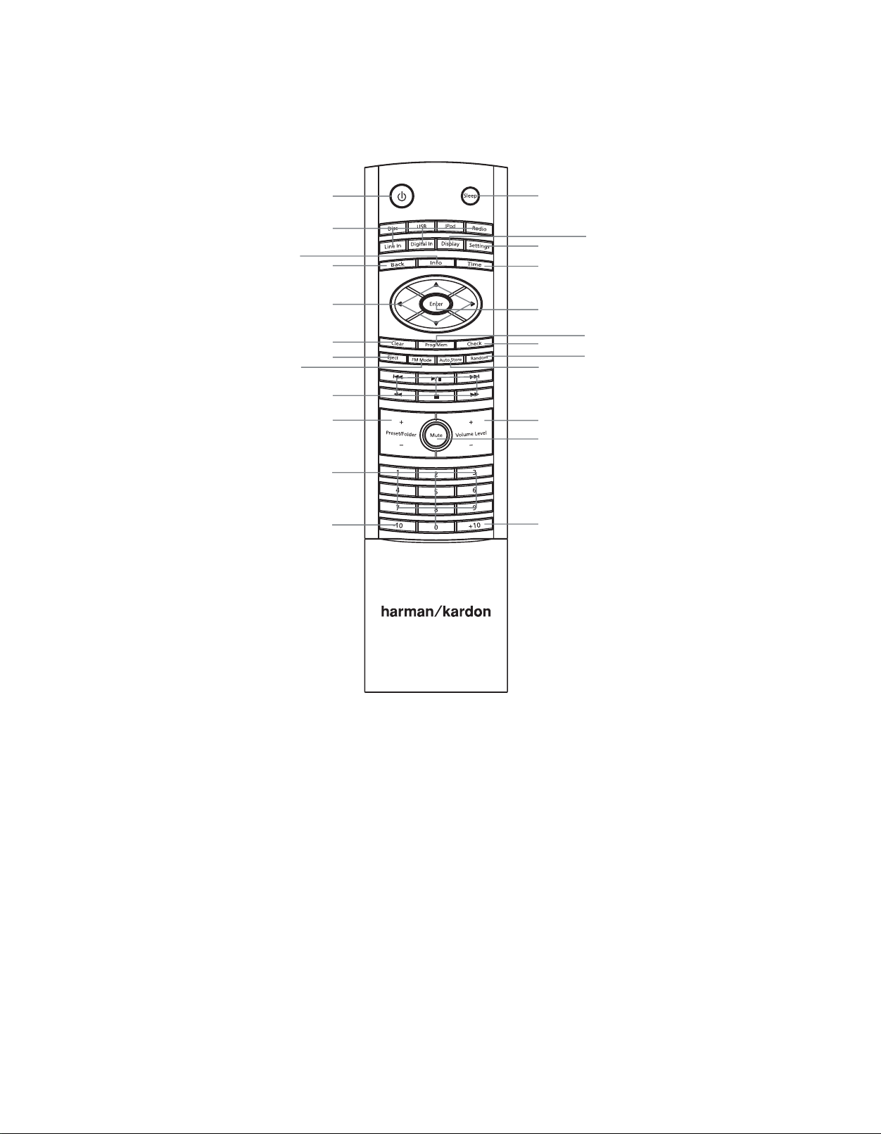
Remote control functions
Source Selectors
K/LM/N
FM Mode
Transport Controls
Preset/Folder +/–
–10 numeric Key
Power
Info
Back
Navigation
Clear
Eject
Numeric keys
Sleep
Settings
Time
Enter
Check
Auto Store
Volume +/–
Mute
+10 numeric Key
Display
Program/Memory
Random
Power: Turns the MAS system on or off. To completely power off the unit, unplug the
power supply.
Sleep: Each press increases the time until turn-off, from 10 to 90 minutes, in increments
of 10 minutes. The next press after the 90 minutes setting turns off the Sleep function.
Source Selectors: Selects a source input. Each press of the Line In or Digital In button
toggles among the available analog (L ine Input on right-side panel; TV, AUX or Phono
Input on rear panel) or digital audio inputs (Coaxial 1 or 2, Optical 1 or 2), respectively.
Press the iPod button to select an iPod docked in The Bridge IIIP.
Display: Adjusts the brightness of the message display. Each time the button is pressed
and held for one second, the message display brightness will cycle between full, half and
off. When the display is off while the system is turned on, the LEDs inside the Volume
knob and behind the front-panel function buttons will remain lit to remind you that the
system is still on.
Settings: Accesses menus for Speaker Setup (tone controls), Time Setup (clock), Alarm
Setup, System Version and System Reset. See the Operation section for more information.
Back: Returns to previous menu level.
Info: Displays the status of the current source:
Radio
•
: When FM band is in use, each press of the button toggles between the PS
(Program Service) and RT (Radio Text) RDS information, if available. When a DAB
radio station is playing (MAS 111 only), press this button to access the menu system
for the DAB tuner. See pages 13 and 14 for more information.
Audio CD
•
•
Time: Displays elapsed track time for the current Audio CD (no effect on data CDs or
other sources). Each additional press changes the display as follows: remaining track
time, elapsed disc time, remaining disc time then back to elapsed track time.
K/LM/N
through the Settin gs Menus, or through lists of content, and press the Enter button to
make selections. Press the Back button to return to the previous menu or content level.
Enter: Selects a menu item, or saves setting changes and returns to the previous menu
level.
: Displays CD Text information, if available. Each press of the button displays
the following items: Song, Artist, Album.
USB or Data CD
press of the button displays the individual items Song, Artist, Album, File type and
Folder, and then goes back to scrolling. If ID3 tags are not available, the file name will
appear.
: Scrolls all ID3 tag information for current source, if available. Each
Navigation buttons: Use the M and N buttons to scroll forward and reverse
Page 9

7
ENGLISH
MAS SySteM
Clear: Clears the current preset station or a playlist entry.
Radio
•
: To delete the current preset station, press the Clear button while it is playing.
Playlist
•
Program/Memory: Used to program playlists and radio presets.
•
•
Check: After a playlist has been programmed and play has been stopped, each press of
the Check button displays the tracks in the playlist.
Eject: When a CD is loaded, press this button to eject it.
FM Mode: Used with FM radio, each press toggles between Stereo and Monaural
playback.
Auto Store: Scans through all frequencies, searching for stations with acceptably strong
signal quality, and stores them as presets.
Random: Each press turns Random playback mode (shuffle) on or off. This mode plays
the tracks of the current disc or drive in random order.
: While programming a playlist, press the Clear button to delete the track just
entered. After the playlist has been saved by pressing the Stop button, press the Clear
button to delete the entire playlist. To delete a single track, stop play, press the Check
button repeatedly until the desired track appears and press the Clear button. Press
the Play or Stop button to exit the Check mode.
Radio
: If the current station has not been programmed into a preset, press Program/
Memory and press the Enter button to store the station at the current preset number,
or use the numeric keys to enter a different preset number. The new preset will
overwrite the existing one.
USB or CD (Audio or Data)
tracks to the playlist by using the Skip/Scan Transpor t Controls or the numeric keys
to select the t rack, then press the Program button to enter t he selection. Add up to
30 files. Press Play to play the playlist, or Stop to save the playlist without playing it.
During playback, the order of the track in the playlist will appear on the left, with the
disc’s track number to the right. See page 14 and 15.
: Press the Program button to begin Program Mode. Add
Remote control functions
Transport Controls
Track Skip Up/Down (iPod, CD or USB): Press and release the Next/Previous
skip buttons to skip to the next track, or the beginning of the current track. Press the
Previous Skip button twice to skip to the previous track.
Scan Forward/Reverse: These buttons function differently, depending on which
source has been selected:
iPod, CD or USB
•
track.
•
Radio:
by one increment/decrement. Press and hold a button to scan quickly through
the frequencies for next available station. Press the same button again to stop
scanning.
Play/Pause: Each tap toggles between the Play and Pause functions.
Stop: Fully stops playback.
Preset/Folder +/–: Selects a preset station or folder on a USB or data CD.
Radio
•
: Each press changes to the next or previous preset station, if any have been
programmed.
USB or Data CD
•
to the next or previous folder. After 3 seconds, the first track in the new folder will
begin playing.
Mute: Press to temporarily silence the speakers. Press again to restore audio. Muting is
also canceled if the MAS system is turned off.
NOTE: Pressing the Mute button also mutes the Analog Audio Outputs. See page 6.
Volume +/–: Increases or decreases the volume. Press and hold to change the volume
more quickly.
Numeric keys: Used to enter track numbers, radio stations or preset numbers, or while
adjusting the clock and alarm times.
–10 and +10 numeric Key: Used with a USB device or CD to quickly advance through a
large number of tracks. Each press of these keys changes to the next or previous track in
increments of 10.
: Press and hold a button to scan forward or reverse within a
Press and release a button to tune to the next higher or lower frequency
: Press once to open the current folder. Each additional press changes
Page 10
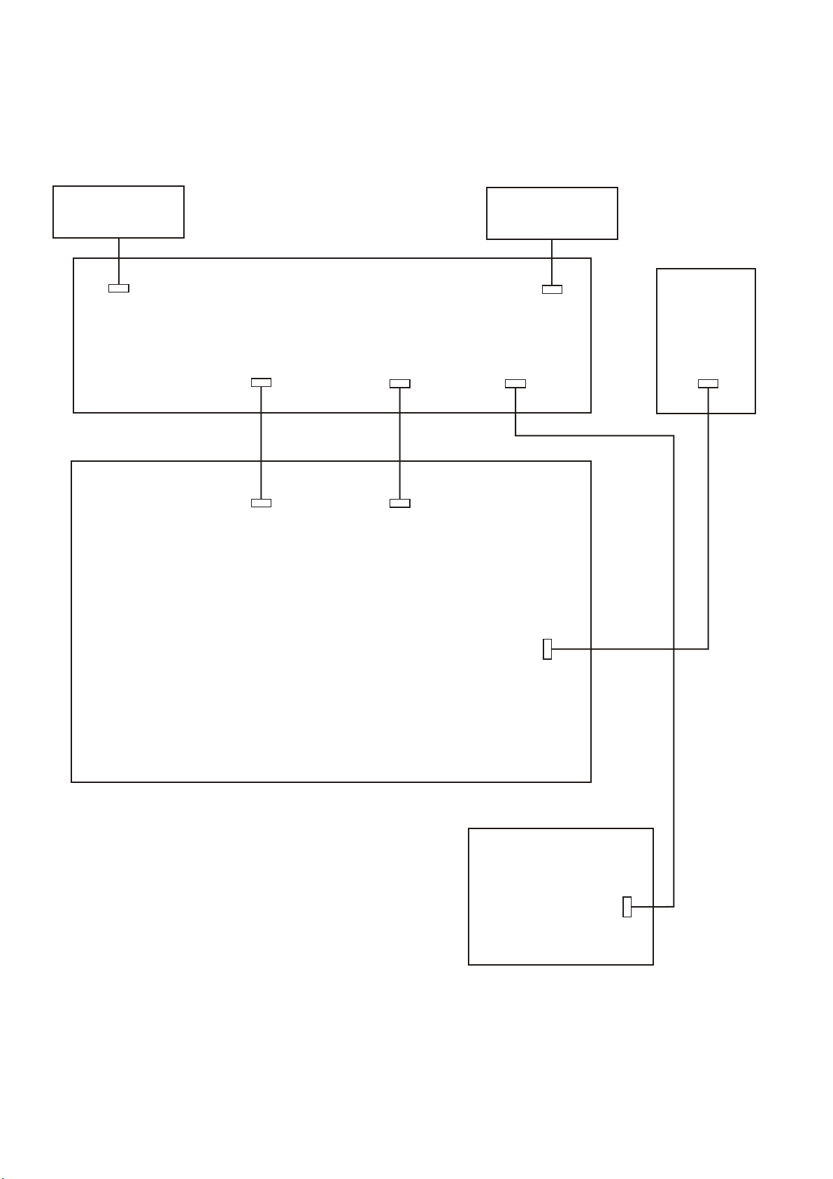
SPEAKER JOINT
8
WIRING DIAGRAM
BOARD
SPEAKER JOINT
BOARD
CN4
2P
AMP BOARD
CN3
9P
CN3
9P
POWER BOARD
CN1
6P
CN2
6P
CN5
2P
FUSE
CN2
4P
CN1
2P
VOL BOARD
CN3
4P
Page 11
Please click here to visit our online spice models database.
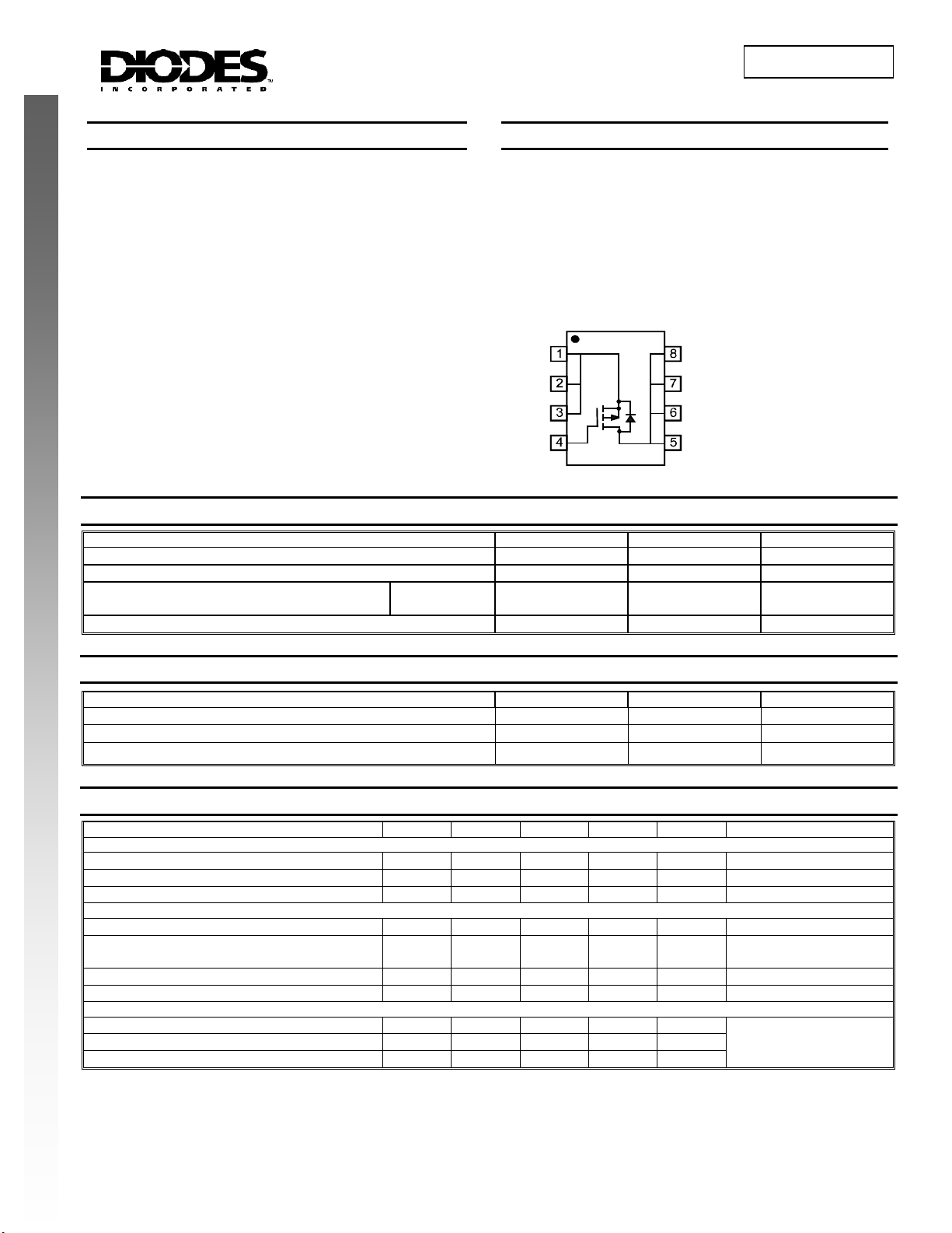
Features
• Low On-Resistance
• 14mΩ @ V
• 25mΩ @ V
= -10V
GS
= -4.5V
GS
• Low Gate Threshold Voltage
• Low Input Capacitance
• Fast Switching Speed
• Low Input/Output Leakage
• Lead Free By Design/RoHS Compliant (Note 2)
• "Green" Device (Note 4)
• Qualified to AEC-Q101 Standards for High Reliability
NEW PRODUCT
Maximum Ratings @T
Drain-Source Voltage
Gate-Source Voltage
Drain Current (Note 1) Steady
State
Pulsed Drain Current (Note 3)
= 25°C unless otherwise specified
A
Characteristic Symbol Value Units
DMP3020LSS
SINGLE P-CHANNEL ENHANCEMENT MODE FIELD EFFECT TRANSISTOR
Mechanical Data
• Case: SOP-8L
• Case Material: Molded Plastic, “Green” Molding Compound.
UL Flammability Classification Rating 94V-0
• Moisture Sensitivity: Level 1 per J-STD-020D
• Terminals Connections: See Diagram
• Terminals: Finish - Matte Tin annealed over Copper lead
frame. Solderable per MIL-STD-202, Method 208
• Marking Information: See Page 3
• Ordering Information: See Page 3
• Weight: 0.072g (approximate)
TOP VIEW
= 25°C
T
A
= 70°C
T
A
SOP-8L
S
S
S
G
Internal Schematic
V
DSS
V
GSS
I
D
I
DM
TOP VIEW
D
D
D
D
-30 V
±20
-12
-6
-40 A
V
A
Thermal Characteristics
Characteristic Symbol Value Unit
Total Power Dissipation (Note 1)
Thermal Resistance, Junction to Ambient
Operating and Storage Temperature Range
Electrical Characteristics @T
OFF CHARACTERISTICS (Note 5)
Drain-Source Breakdown Voltage
Zero Gate Voltage Drain Current
Gate-Source Leakage
ON CHARACTERISTICS (Note 5)
Gate Threshold Voltage
Static Drain-Source On-Resistance
Forward Transconductance
Diode Forward Voltage (Note 5)
DYNAMIC CHARACTERISTICS
Input Capacitance
Output Capacitance
Reverse Transfer Capacitance
Notes: 1. Device mounted on 2 oz. Copper pads on FR-4 PCB with R
2. No purposefully added lead.
3. Pulse width ≤10μS, Duty Cycle ≤1%.
4. Diodes Inc.'s "Green" policy can be found on our website at http://www.diodes.com/products/lead_free/index.php.
5. Short duration pulse test used to minimize self-heating effect.
DMP3020LSS
Document number: DS31263 Rev. 4 - 2
Characteristic Symbol Min Typ Max Unit Test Condition
= 25°C unless otherwise specified
A
θJA
-30
-1
⎯
⎯
-0.5
= 50°C/W.
BV
DSS
I
⎯ ⎯
DSS
I
⎯ ⎯
GSS
V
GS(th)
R
DS (ON)
g
⎯
fs
V
SD
C
⎯
iss
C
⎯
oss
C
⎯
rss
www.diodes.com
9
P
D
R
JA
θ
T
J, TSTG
⎯ ⎯
⎯
11.6
18.6
12
⎯
1655
286
240
-55 to +150 °C
-1
±100
-2 V
14
25
⎯
-1.1 V
⎯
⎯
⎯
2.5 W
50 °C/W
V
V
= 0V, ID = -250μA
μA
nA
mΩ
S
GS
= -30V, VGS = 0V
V
DS
V
= ±20V, VDS = 0V
GS
V
= VGS, ID = -250μA
DS
V
= -10V, ID = -8A
GS
V
= -4.5V, ID = -5A
GS
V
= -10V, ID = -12A
DS
VGS = 0V, IS = -2A
pF
V
= -20V, VGS = 0V
pF
pF
DS
f = 1.0MHz
© Diodes Incorporated
May 2008
Page 12
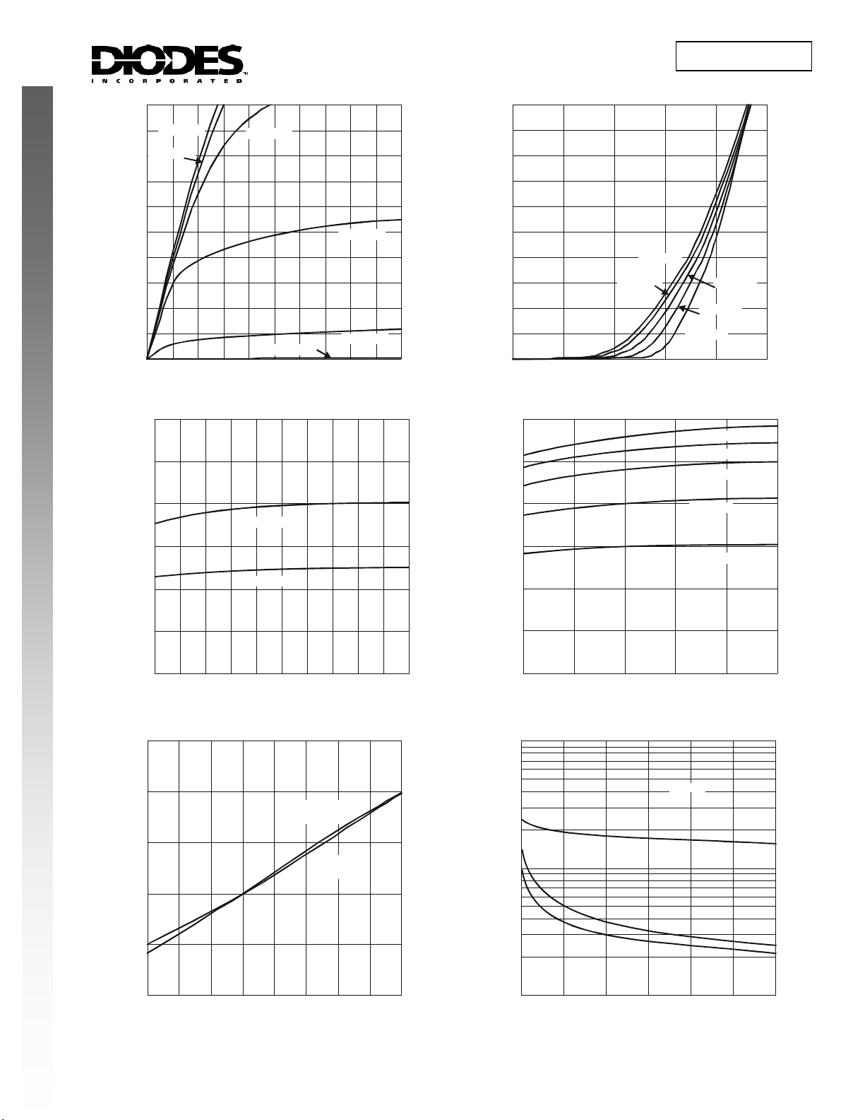
RAIN CUR
REN
T
R
CUR
RENT
R
RAIN-SOUR
CE O
N-R
TAN
C
R
R
OUR
CE ON-R
TANC
C
C
PACITAN
C
F
20
V = -10V
GS
V = -4.0V
GS
16
(A)
12
8
D
-I , D
4
NEW PRODUCT
0
01234
-V , DRAIN-SOURCE VOLTAGE (V)
DS
Fig. 1 Typical Output Characteristic
0.03
Ω
E ( )
0.025
V = -3.0V
GS
V = -1.5V
GS
V = -2.5V
GS
V = -2.0V
GS
5
DMP3020LSS
20
16
(A)
12
8
AIN
D
-I , D
4
0
1 1.5 2 2.5 3 3.5
-V , GATE-SOURCE VOLTAGE (V)
GS
Fig. 2 Typical Transfer Characterist ic
0.03
Ω
E ( )
0.025
T = 150°C
A
T = 125°C
A
T = 25°C
A
T = -55°C
A
T = 150°C
T = 125°C
A
T = 85°C
A
T = 85°C
A
A
DS(ON)
R , DRAIN-SOURCE
ESIS
0.02
V = -4.5V
GS
0.015
V = -10V
0.01
, D
0.005
DS(ON)
0
0 6 12 18 24 30
-I , DRAIN-SOURCE CURRENT (A)
D
Fig. 3 Typical On-Resistance
GS
vs. Drain Current and Gate Voltage
1.6
1.4
V = -10V
GS
I = -10A
D
1.2
V = -4.5V
1.0
0.8
ON-RESISTANCE (NORMALIZED)
GS
I = -5A
D
0.02
ESIS
0.015
T = 25°C
A
T = -55°C
A
0.01
AIN-S
0.005
, D
DS(ON)
0
0 6 12 18 24 30
-I , DRAIN CURRENT (A)
D
Fig. 4 Typical On-Resistance
vs. Drain Current and Temperature
10,000
f = 1MHz
)
E (p
C
iss
1,000
A
,
C
oss
C
rss
0.6
-50 -25 0 25 50 75 100 125 150
T , AMBIENT TEMPERATURE (°C)
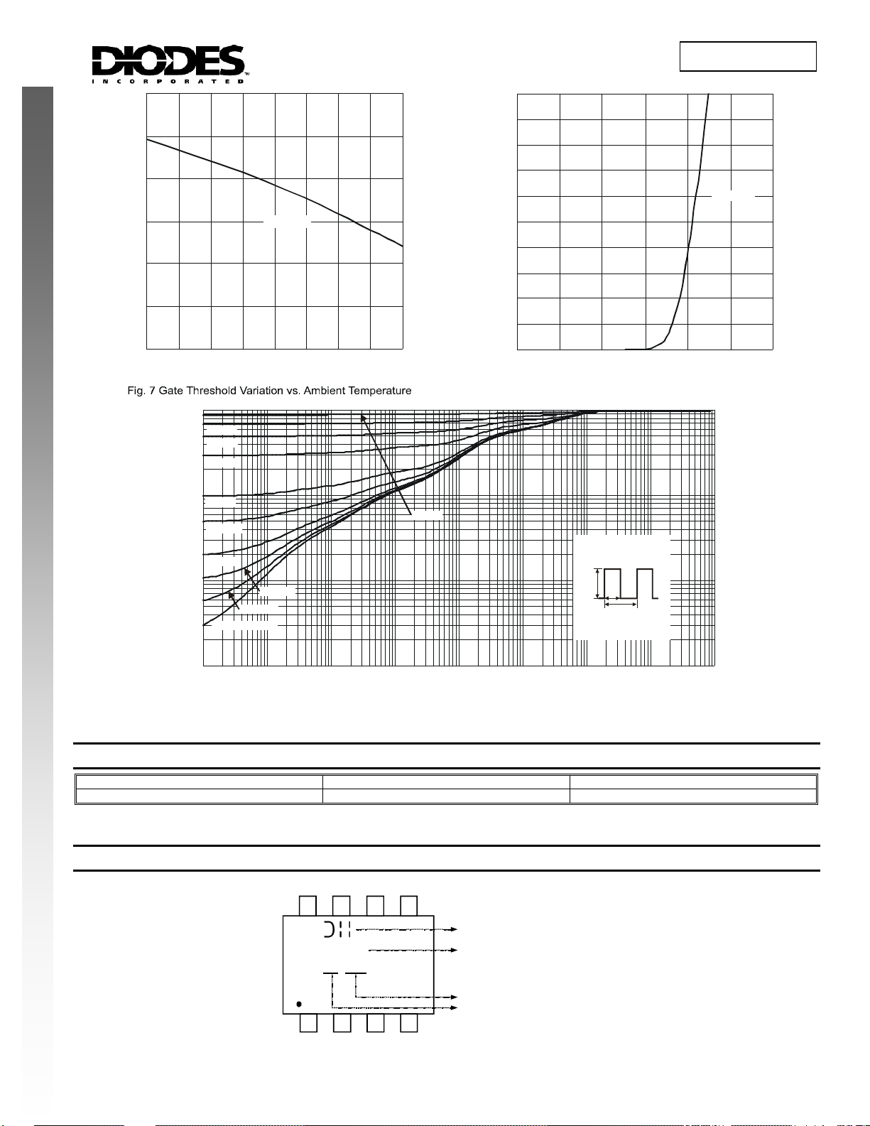
DMP3020LSS
Document number: DS31263 Rev. 4 - 2
Fig. 5 Normalized On-Resistance vs. Ambient Temperature
A
www.diodes.com
10
100
0 5 10 15 20 25 30
V , DRAIN-SOURCE VOLTAGE (V)
DS
Fig. 6 Typical Total Capaci tance
May 2008
© Diodes Incorporated
Page 13
OUR
CE CUR
REN
T
T
R
T T
HER
R
TANC
2.4
2.0
1.6
1.2
0.8
0.4
GS(TH)
-V , GATE THRESHOLD VOLTAGE (V)
0
NEW PRODUCT
-50 -25 0 25 50 75 100 125 150
T , AMBIENT TEMPERATURE (°C)
A
1
E
ESIS
0.1
MAL
0.01
ANSIEN
r(t),
0.001
0.0001 0.001 0.01 0.1 1 10 100 1,000 10,000
D = 0.7
D = 0.5
D = 0.3
D = 0.1
D = 0.05
D = 0.02
D = 0.005
D = Single Pulse
I = -250µA
D
D = 0.01
20
16
(A)
12
8
S
-I , S
4
0
0 0.2 0.4 0.6 0.8 1 1.2
D = 0.9
t , PULSE DURATION TIME (s)
1
Fig. 9 Transient Thermal Response
DMP3020LSS
T = 25°C
A
-V , SOURCE-DRAIN VOLTAGE (V)
SD
Fig. 8 Diode Forward Voltage vs. Current
R (t) = r(t) * R
θθ
JA JA
R = 87°C/W
θ
JA
P(pk)
t
1
t
2
T - T = P * R (t)
JA JA12θ
Duty Cycle, D = t /t
Ordering Information (Note 6)
Part Number Case Packaging
DMP3020LSS-13 SOP-8L 2500/Tape & Reel
Notes: 6. For packaging details, go to our website at http://www.diodes.com/datasheets/ap02007.pdf.
Marking Information
DMP3020LSS
Document number: DS31263 Rev. 4 - 2
Top View
8 5
P3020LS
YY
WW
1 4
Logo
Part no.
Xth week: 01~52
Year: "07" =2007
"08" =2008
www.diodes.com
11
May 2008
© Diodes Incorporated
Page 14
DMP3020LSS
Package Outline Dimensions
NEW PRODUCT
e
D
E1
E
A1
DETAIL A
h
45°
A2
A3
A
b
L
0.254
GAUGE PLANE
SEATING PLANE
7°~9°
DETAIL A
SOP-8L
Dim Min Max
A
⎯
1.75
A1 0.08 0.25
A2 1.30 1.50
A3 0.20 Typ.
b 0.3 0.5
D 4.80 5.30
E 5.79 6.20
E1 3.70 4.10
e 1.27 Typ.
h
⎯
0.35
L 0.38 1.27
0° 8°
θ
All Dimensions in mm
Suggested Pad Layout
Diodes Incorporated and its subsidiaries rese rve the right to make modifications, enhanc ements, improvements, corrections or ot her changes
without further notice to any product herein. Diodes Incorporat ed does not assume any liability arising out of the application or use of any product
described herein; neither does it convey any license under its patent rights, nor the rights of others. The user of products in such applications shall
assume all risks of such use and w ill agree to hold Diodes Inco rporated and all the companies w hose products are represented on our w ebsite,
harmless against all damages.
Diodes Incorporated products are not authorized for use as critical components in life support devices or sy stems without the e xpressed written
approval of the President of Diodes Incorporated.
X
Dimensions Value (in mm)
X 0.60
Y 1.55
C1 5.4
C1
C2
Y
C2 1.27
IMPORTANT NOTICE
LIFE SUPPORT
DMP3020LSS
Document number: DS31263 Rev. 4 - 2
www.diodes.com
12
May 2008
© Diodes Incorporated
Page 15

FAN7602
Green Current Mode PWM Controller
FAN7602 Green Current Mode PWM Controller
April 2006
Features
Green Current Mode PWM Control
Fixed 65kHz Operation with Frequency Modulation
Internal High-Voltage Start-up Switch
Burst Mode Operation
Line Voltage Feed Forward to Limit Maximum Power
Line Under-Voltage Protection
Latch Protection & Internal Soft-Start (10ms) Function
Overload Protection
Over Voltage Protection
Low Operation Current: Typ. 1mA
8-pin DIP
Applications
Adapter
LCD Monitor Power
Auxiliary Power Supply
Related Application Notes
AN6014 - Green Current Mode PWM Controller
FAN7602
Description
The FAN7602 is a green current mode PWM controller.
It is specially designed for off-line adapter application,
DVDP, VCR, LCD monitor application, and auxiliary
power supplies.
The internal high-voltage start-up switch and the burst
mode operation reduce the power loss in standby mode.
Because of the internal start-up switch and the burst
mode, it is possible to supply 0.5W load limiting the input
power under 1W when the input line voltage is 265Vac.
On no-load condition, the input power is under 0.3W.
The maximum power can be limited constantly, regardless of the line voltage change using the power limit
function.
The switching frequency is internally fixed to be 65kHz
and the frequency modulation technique reduces EMI.
The FAN7602 includes various protections for the system reliability and the internal soft start prevents the output voltage over-shoot at start-up.
Ordering Information
Operating T emp.
Part Number
FAN7602N -25°C to +125°C Yes 8-DIP Rail FAN7602
©2006 Fairchild Semiconductor Corporation www.fairchildsemi.com
FAN7602 Rev. 1.0.1
Range Pb-Free Package Packing Method
13
Marking
Code
Page 16
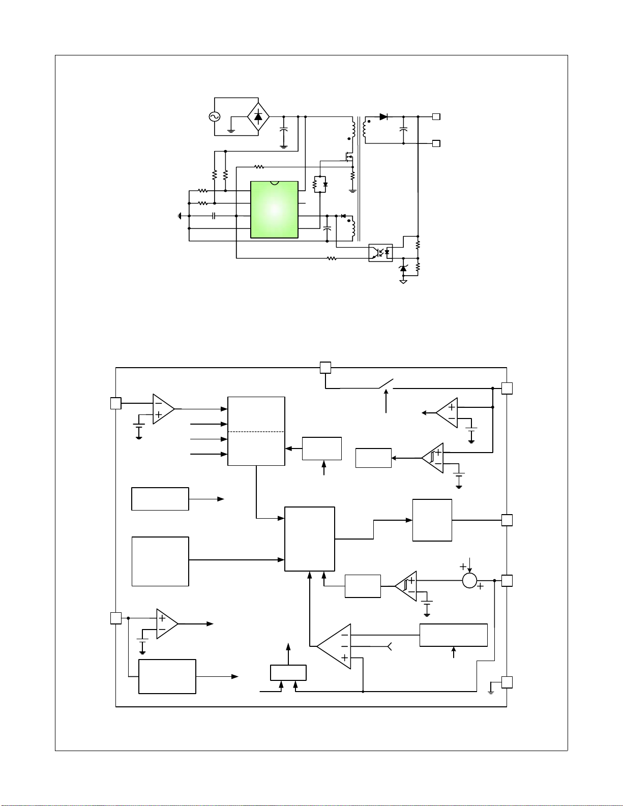
Typical Application Diagram
Figure 1. Typical Flyback Application
Internal Block Diagram
FAN7602 Green Current Mode PWM Controller
FAN7602
LUVP
Latch/
Plimit
1
2
2V/1.5V
10ms
Soft Start
65kHz Clock
with
Frequency
Modulation
4V
Plimit
Offset
Generator
LUVP
Latch
SS End
Latch
OLP
OVP
Plimit
Offset
Auto Restart
Protection
Latch
Protection
Soft
Start
OLP
OLP
Reset
Circuit
PWM
Block
Vstr
Vcc
8
6
Vcc
OVP
5V Ref
Delay
Circuit
PWM+
SS End
0.95V/0.88V
Soft
Start
UVLO
Driver
Circuit
Power Limit
Plimit
Offset
12V/8V
Plimit
Offset
19V
5
3
4
OUT
CS/FB
GND
Figure 2. Functional Block Diagram of FAN7602
FAN7602 Rev. 1.0.1
www.fairchildsemi.com
14
Page 17
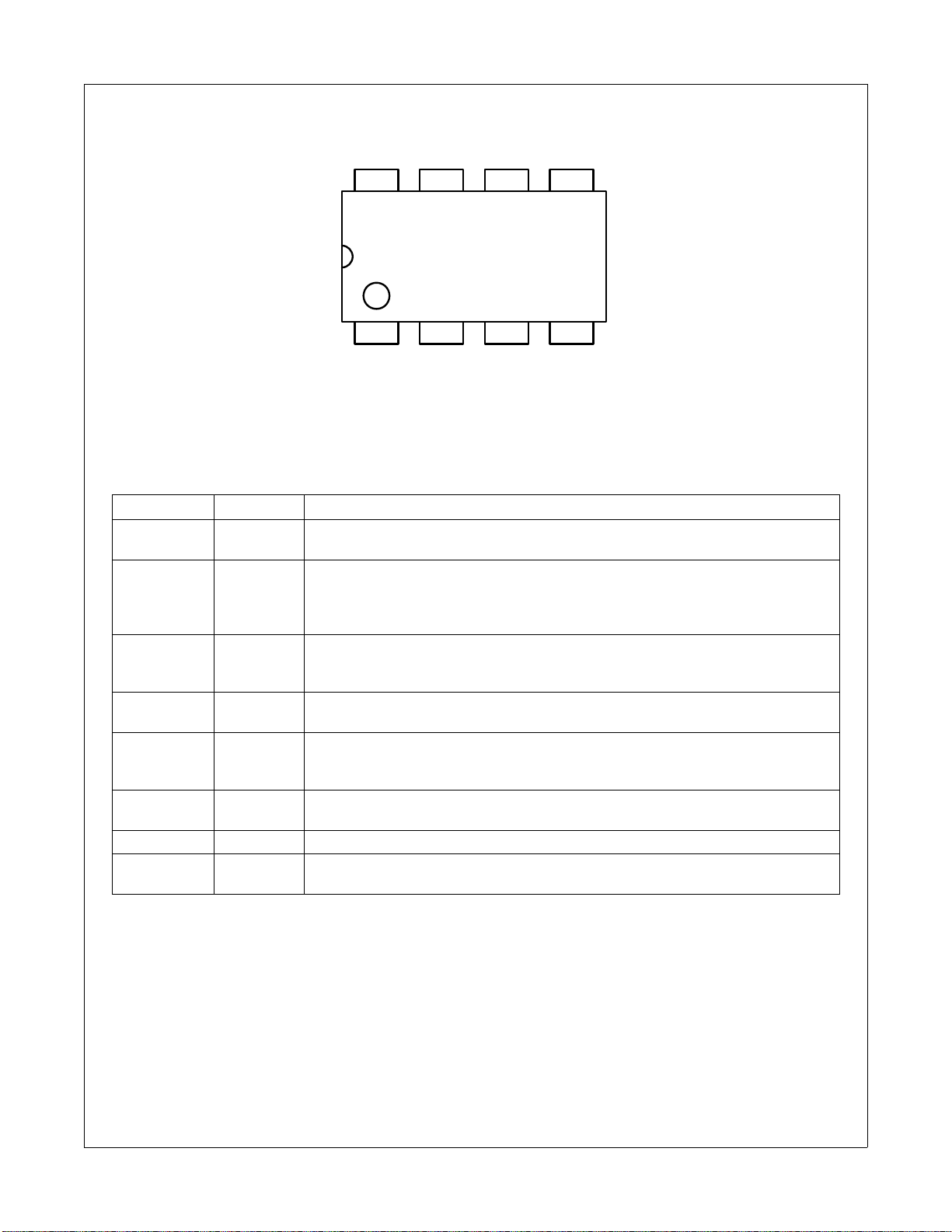
Pin Assignments
Vstr NC Vcc Out
8
7
6
5
FAN7602
YWW
FAN7602 Green Current Mode PWM Controller
1
Figure 3. Pin Configuration (Top View)
2
Latch/
Plimit
3
4
GNDCS/FBLUVP
Pin Definitions
Pin Number Pin Name Pin Function Description
1LUVPLine Under Voltage Protection Pin. This pin is used to protect the set when the
input voltage is lower than the rated input voltage range.
2 Latch/Plimit Latch Protection and Power Limit Pin. When the pin voltage exceeds 4V, the latch
protection works and the latch protection is re set when the Vcc voltage is lowe r than
5V. For the power limit function, the OCP level decreases as the pin voltage
increases.
3CS/FBCurrent Sense and Fee dback Pin. This pin is used to sense the MOSFET current
for the current mode PWM and OCP. The output volta ge feedback information and
the current sense information are added using external RC filter.
4GNDGround Pin. This pin is used for the ground potential of all the pins. For proper oper-
ation, the signal ground and the power ground should be separated.
5OUTGate Drive Output Pin. This pin is an output pin to drive an external MOSFET. The
peak sourcing current is 450mA and the peak sinking current is 600mA. For prop er
operation, the stray inductance in the gate driving path must be minimized.
6VccSupply Voltage Pin. IC operating current and MOSFET driving current are supplied
using this pin.
7NCNo Connection.
8 Vstr Start-up Pin. This pin is used to supply IC operating current during IC start-up. After
start-up, the internal JFET is turned off to reduce power loss.
FAN7602 Rev. 1.0.1
www.fairchildsemi.com
15
Page 18
FSFR-Series — Fairchild Power Switch (FPS™)
for Half-Bridge Resonant Converters
FSFR-Series — Fairchild Power Switch (FPS
April 2009
Features
Variable Frequency Control with 50% Duty Cycle
for Half-Bridge Resonant Converter Topology
High Efficiency through Zero Voltage Switching (ZVS)
Internal SuperFET™s with Fast-Recovery Type
Body Diode (t
with Fast-Recovery Type Body Diode (t
FSFR2100U/2000/1900/1800/1700.
=120ns) for FSFR2100 and UniFETs
rr
<160ns) for
rr
Fixed Dead Time (350ns) Optimized for MOSFETs
Up to 300kHz Operating Frequency
Pulse Skipping for Frequency Limit (Programmable)
at Light-Load Condition
Remote On/Off Control Using Control Pin
Protection Functions: Over-Voltage Protection
(OVP), Over-Load Protection (OLP), Over-Current
Protection (OCP), Abnormal Over-Current Protection
(AOCP), Internal Thermal Shutdown (TSD)
Applications
PDP and LCD TVs
Desktop PCs and Servers
Adapters
Telecom Power Supplies
Audio Power Supplies
Description
The FSFR-series are a highly integrated power switches
designed for high-efficiency half-bridge resonant
converters. Offering everything necessary to build a
reliable and robust resonant converter, the FSFR-series
simplifies designs and improves productivity, while
improving performance. The FSFR-series combines
power MOSFETs with fast-recovery type body diodes, a
high-side gate-drive circuit, an accurate current
controlled oscillator, frequency limit circuit, soft-start, and
built-in protection functions. The high-side gate-drive
circuit has a common-mode noise cancellation
capability, which guarantees stable operation with
excellent noise immunity. The fast-recovery body diode
of the MOSFETs improves reliability against abnormal
operation conditions, while minimizing the effect of the
reverse recovery. Using the zero-voltage-switching (ZVS)
technique dramatically reduces the switching losses and
efficiency is significantly improved. The ZVS also
reduces the switching noise noticeably, which allows a
small-sized Electromagnetic Interference (EMI) filter.
The FSFR-series can be applied to various resonant
converter topologies such as series resonant, parallel
resonant, and LLC resonant converters.
Related Resources
AN4151 — Half-bridge LLC Resonant Converter Design
using FSFR-series Fairchild Power Switch (FPSTM)
™
) for Half-Bridge Resonant Converter
Ordering Information
Part
Number
FSFR2100
FSFR2100U
FSFR2000
FSFR1900
FSFR1800
FSFR1700
Notes:
1. The junction temperature can limit the maximum output power.
2. Maximum practical continuous power in an open-frame design at 50°C ambient.
For Fairchild’s definition of Eco Status, please visit: http://www.fairchildsemi.com/company/green/rohs_green.html.
© 2007 Fairchild Semiconductor Corporation www.fairchildsemi.com
FSFR series • Rev.1.0.5
Package
9-SIP
Eco
Status
RoHS
Operating
Junction
Temperature
-40 to +130°C
R
DS(ON_MAX)
0.38Ω
0.51Ω
0.67Ω
0.85Ω
0.95Ω
1.25Ω
Maximum Output Power
without Heatsink
=350~400V)
(V
IN
200W 450W
180W 400W
160W 350W
140W 300W
120W 260W
100W 200W
16
(1,2)
Maximum Output Power
with Heatsink
(VIN=350~400V)
(1,2)
Page 19

Application Circuit Diagram
s
μ
V
CC
RT
LVcc
FSFR-Series — Fairchild Power Switch (FPS™) for Half-Bridge Resonant Converter
Ns
Ns
D1
Vo
Cr
L
lk
Np
V
DL
Lm
HV
CC
C
DL
V
IN
Figure 1. Typical Application Circuit (LLC Resonant Half-Bridge Converter)
Block Diagram
CON
CS
R
sense
Control
IC
SG PG
R
D2
V
CTR
KA431
FCF
1.5
Figure 2. Internal Block Diagram
© 2007 Fairchild Semiconductor Corporation www.fairchildsemi.com
FSFR series • Rev.1.0.5
17
Page 20

Pin Configuration
1 2 3 4 5 6 7 8 9 10
CSSGPG
LVcc
HVcc
CON
R
T
V
DL
Figure 3. Package Diagram
FSFR-Series — Fairchild Power Switch (FPS™) for Half-Bridge Resonant Converter
V
CTR
Pin Definitions
Pin # Name Description
1 VDL This is the drain of the high-side MOSFET, typically connected to the input DC link voltage.
This pin is for enable/disable and protection. When the voltage of this pin is above 0.6V, the
2 CON
3 RT
4 CS
5 SG This pin is the control ground.
6 PG This pin is the power ground. This pin is connected to the source of the low-side MOSFET.
7 LVCC This pin is the supply voltage of the control IC.
8 NC No connection.
9 HVCC This is the supply voltage of the high-side gate-drive circuit IC.
10 V
CTR
IC operation is enabled. When the voltage of this pin drops below 0.4V, gate drive signals
for both MOSFETs are disabled. When the voltage of this pin increases above 5V,
protection is triggered.
This pin programs the switching frequency. Typically, an opto-coupler is connected to
control the switching frequency for the output voltage regulation.
This pin senses the current flowing through the low-side MOSFET. Typically, negative
voltage is applied on this pin.
This is the drain of the low-side MOSFET. Typically, a transformer is connected to this pin.
© 2007 Fairchild Semiconductor Corporation www.fairchildsemi.com
FSFR series • Rev.1.0.5
18
Page 21

September 2007
IRS2092
Features
• Integrated analog input Class D audio amplifier
driver in a small 16 pin package
• Floating inputs enable easy half bridge
implementation
• Programmable bidirectional over-current
protection with self-reset function
• Programmable preset deadtime for improved
THD performances
• Start and stop click noise reduction
• High noise immunity
• ±100 V ratings deliver up to 500 W in output
power
• Operates up to 800 kHz
• RoHS compliant
Typical Applications
• Home theater systems
• Mini component stereo systems
• Powered speaker systems
• General purpose audio power amplifiers
PROTECTED DIGITAL AUDIO AMPLIFIER
Product Summary
V
Selectable Deadtime 25/40/65/105 ns
OC protection delay (max) 500 ns
DC offset <20 mV
PWM frequency ~800 kHz
Error amplifier open loop gain >60 dB
THD+N* (1kHz, 50W, 4Ω) 0.01 %
Residual Noise*
(AES-17 Filter)
* measured with recommended circuit
OFFSET
(max)
Gate driver
± 100 V
Io+ 1.0 A
Io - 1.2 A
200 µVrms
Package Options
SOIC16N PDIP16
Typical Connection Diagram
INPUT
IRS2092
VAA
2
GND
3
IN-
4
COMP
5
CSD
6
VSS
7
VREF
8
OCSET
CSH
VB
HO
VS
VCC
LO
COM
DT
161
15
14
13
12
11
10
9
+B
Vcc
12V
-B
Speaker
www.irf.com © 2007 International Rectifier
19
Page 22

20
Page 23

21
Page 24

Product Specification
Power Factor Controller
SG6961
FEATURES
Boundary Mode PFC Controller
Low Input Current THD
Controlled On-Time PWM
Zero-Current Detection
Cycle-by-Cycle Current Limiting
Leading-Edge Blanking Instead of RC Filtering
Low Start-up Current (10µA Typical)
Low Operating Current (4.5mA Typical)
Feedback Open-Loop Protection
Programmable Maximum On-Time (MOT)
Output Over-Voltage Clamping Protection
Clamped Gate Output Voltage 16.5V
APPLICATIONS
Electric Lamp Ballasts
AC-DC Switching Mode Power Converter
Open -Frame Power Supplies and Power Adapters
Flyback Power Converters with ZCS/ZVS
DESCRIPTION
The SG6961 is an 8-pin boundary mode PFC controller IC
intended for controlling PFC pre-regulators. The SG6961
provides a controlled on-time to regulate the output DC
voltage and achieve natural power factor correction. The
maximum on-time of the extern al swit ch is programmable
to ensure safe operation during AC brownouts. An
innovative multi-vector error amplifier is built in to
provide rapid transient response and precise output
voltage clamping. A built-in circuit disables the controller
if the output feedback loop is opened. The s tart-up cu rrent
is lower than 20µA and the operating current is under
4.5mA. The supply voltage can be up to 20V, maximizing
application flexibility.
TYPICAL APPLICATION
VAC
VCC
MOT
ZCD
COMP
SG6961
GND
Vo
INV
GD
CS
© System General Corp. www.sg.com.tw • www.fairchildsemi.com
Version 1.3.1 (IRO33.0028.B6) September 24, 2007
22
Page 25

Product Specification
Power Factor Controller
MARKING DIAGRAMS PIN CONFIGURATION
T: D=DIP, S=SOP
SG6961TP
XXXXXXXXYWWV
P : Z=Lead Free + ROHS
Compatible
Null=regular package
XXXXXXXX: Wafer Lot
Y: Year; WW: Week
V: Assembl y Locat i on
INV
COMP
MOT
SG6961
VCC
GD
GND
CS
ZCD
ORDERING INFORMATION
Part Number Pb-Free Package
SG6961SZ
SG6961DZ
8-Pin SOP
8-Pin DIP
PIN DESCRIPTIONS
Pin No. Symbol Descri pti on
1 INV
2 COMP
3 MOT
4 CS
5 ZCD
6 GND
7 GD Totem-pole driver output to drive the external power MOSFET. The clamped gate output voltage is 16.5V.
8 VCC Dri ver and control circuit supply voltage.
Inverting input of the error amplifier . INV is conne c ted to the converter output via a resisti ve divider. This pin
is also used for over-voltage clamping and open-loop feedback protection.
The output of the error amplifier. To create a precise clamping protection , a compensation network between
this pin and GND is suggested.
A resistor from MOT to GND is use d to determine the maximum on-t ime of the exter nal pow er MOSFET. The
maximum output power of the converter is a function of the maximum on-time.
Input to the over-current protection comparator . When the sen sed volta ge acro ss the sen se resist or reaches
the internal threshold (0.82V), the switch is turned off to activate cycle-by-cycle current limiting.
Zero Current Detection. This pin is connec ted to an auxil iary wind ing via a re sistor to de tect the z ero crossing
of the switch current. When the zero crossing is detected, a new switching cycle is started. If it is connected
to GND, the device is disabled.
The power ground and signal gr ound. Placing a 0.1µF d e coupling capacitor betw ee n the VCC
is recommended.
and GND pins
© System General Corp. www.sg.com.tw • www.fairchildsemi.com
Version 1.3.1 (IRO33.0028.B6) September 24, 2007
23
Page 26

Product Brief
ADJUSTABLE PRECISION SHUNT REGULATORS AZ431-A
Description
The AZ431-A series ICs are three-terminal adjustable
shunt regulators with guaranteed thermal stability over a
full operation range. These ICs feature sharp turn -on characteristics, low temperature coefficient and low output
impedance, which make them ideal substitutes for Zener
diodes in applications such as switching power supply,
charger and other adjustable regulators.
The AZ431-A series ICs are of 40V voltage type. Its output voltage can be set to any value between V
REF
(2.5V)
and 36V.
The AZ431-A precision reference is offered in two bandgap tolerance: 0.4% and 0.8%.
Features
· Programmable Precise Output Voltage from 2.5V to
36V
· Very Accurate Reference Voltage: 0.15% Typical
· High Stability under Capacitive Load
· Low Temperature Deviation: 4.5mV Typical
· Low Equivalent Full-range Temperature Coefficient
with 20PPM/
· Low Dynamic Output Resistance: 0.2Ω Typical
· Sink Current Capacity from 1mA to 100 mA
· Low Output Noise
· Wide Operating Range of -40 to 125
o
C T ypi cal
o
C
Parametric Table
AZ431A-A AZ431B-A
I
(Max) (mA)
KA
(Min) (mA)
I
KA
/ V
V
OUT
REF
Initial
100 100
0.4 0.4
0.4 0.8
Tol. (%)
(Max) (V)
V
OUT
(Min) (V)
V
OUT
Z
(Typ) (Ω)
KA
Temp Coeff. (Typ)
o
(PPM/
C)
Operating Temperature
o
(Min) (
C)
Operating Temperature
(Max) (
o
C)
36 36
2.5 2.5
0.15 0.15
20 20
-40 -40
+125 +125
Benefits
· Easier to Stabilize
· Ultra Low Temperature Coefficient
· Higher V
· Wider Operating Temperature Range
· Very Competitive Price
Accuracy
REF
Applications
· Charger
· Voltage Adapter
· Switching Power Supply
· Graphic Card
· Precision Voltage Reference
Additional Available Materials
· Samples
· Datasheet
· Reliability Report
· ESD Report
Pin Configuration
SOT-23-3 SOT-89
ANODE
3
2
1
REF CATHODE
2
1
REF ANODE CATHODE
Nov. 2004 BCD Semiconductor Manufacturing Limited
3
24
Page 27

10 mV
TL071CD
TL071CP
TL071CPWLE
0°C t
10 mV
TL072CD
TL072CP
TL072CPWLE
70°C
10 mV
TL074CD
TL074CN
TL074CPWLE
40°C t
TL071ID
TL071IP
85°C
55°C to
125 C
TL071, TL071A, TL071B, TL072
TL072A, TL072B, TL074, TL074A, TL074B
LOW-NOISE JFET-INPUT OPERATIONAL AMPLIFIERS
SLOS080D – SEPTEMBER 1978 – REVISED AUGUST 1996
D
Low Power Consumption
D
Wide Common-Mode and Differential
Voltage Ranges
D
Low Input Bias and Offset Currents
D
Output Short-Circuit Protection
D
Low Total Harmonic Distortion
0.003% Typ
description
The JFET-input operational amplifiers in the TL07_ series are designed as low-noise versions of the TL08_
series amplifiers with low input bias and offset currents and fast slew rate. The low harmonic distortion and low
noise make the TL07_ series ideally suited for high-fidelity and audio preamplifier applications. Each amplifier
features JFET inputs (for high input impedance) coupled with bipolar output stages integrated on a single
monolithic chip.
The C-suffix devices are characterized for operation from 0°C to 70°C. The I-suffix devices are characterized
for operation from – 40°C to 85°C. The M-suffix devices are characterized for operation over the full military
temperature range of –55°C to 125°C.
D
Low Noise
V
= 18 nV/√Hz Typ at f = 1 kHz
n
D
High Input Impedance...JFET Input Stage
D
Internal Frequency Compensation
D
Latch-Up-Free Operation
D
High Slew Rate...13 V/µs Typ
D
Common-Mode Input Voltage Range
Includes V
CC+
AVAILABLE OPTIONS
PACKAGE
T
–
–
†
The D package is available taped and reeled. Add the suffix R to the device type (e.g., TL071CDR). The PW package is only available left-ended
taped and reeled (e.g., TL072CPWLE).
VIOmax
A
AT 25°C
10 mV TL071CD TL071CP TL071CPWLE
6 mV
3 mV TL071BCD TL071BCP —
10 mV TL072CD TL072CP TL072CPWLE
o
°
°
°
°
6 mV
3 mV TL072BCD TL072BCP —
10 mV TL074CD TL074CN TL074CPWLE
6 mV
3 mV TL074BCD TL074BCN —
o
6 mV
6 mV TL071MFK — TL071MJG — — —
6 mV
9 mV TL074MFK TL074MJ — TL074MN — TL074MW
SMALL
OUTLINE
†
(D)
TL071ACD
TL072ACD
TL074ACD
TL071ID — TL071IP
TL072ID
TL074ID TL074IN —
—
CHIP
CARRIER
(FK)
— — — —
— — — —
— — —
— — —
TL072MFK — TL072MJG — TL072MP
CERAMIC
DIP
(J)
CERAMIC
DIP
(JG)
PLASTIC
DIP
(N)
TL074ACN
—
PLASTIC
DIP
(P)
TL071ACP
TL072ACP
—
TL072IP
TSSOP
PACKAGE
(PW)
—
—
—
— —
—
FLAT
PACKAGE
(W)
—
—
—
—
Please be aware that an important notice concerning availability, standard warranty, and use in critical applications of
Texas Instruments semiconductor products and disclaimers thereto appears at the end of this data sheet.
PRODUCTION DATA information is current as of publication date.
Products conform to specifications per the terms of Texas Instruments
standard warranty. Production processing does not necessarily include
testing of all parameters.
POST OFFICE BOX 655303 • DALLAS, TEXAS 75265
25
Copyright 1996, Texas Instruments Incorporated
1
Page 28

262728
Page 29

Page 30

Page 31

FDP20N50 / FDPF20N50
500V N-Channel MOSFET
FDP20N50 / FDPF20N50 500V N-Channel MOSFET
February 2007
TM
UniFET
Features
• 20A, 500V, R
• Low gate charge ( typical 45.6 nC)
•Low C
•Fast switching
• 100% avalanche tested
• Improved dv/dt capability
( typical 27 pF)
rss
= 0.23Ω @VGS = 10 V
DS(on)
S
TO-220
FDP Series
G
D
D
G
Description
These N- Channel enhancement mode power field ef fect
transistors are p roduced using Fairchild’ s pr oprietary, pla nar
stripe, DMOS technology.
This advanced techn ology has been especially tailored to
minimize on-st ate resistance, pr ovide superior switching
performance, and withstand high energy pulse in the avalanche
and commutation mode. These devices are well suited for high
efficient switched mode power supplies and active power factor
correction.
G
S
TO-220F
FDPF Series
S
D
Absolute Maximum Ratings
Symbol Parameter FDP20N50 FDPF20N50 Unit
V
DSS
I
D
I
DM
V
GSS
E
AS
I
AR
E
AR
dv/dt Peak Diode Recovery dv/dt
P
D
T
J, TSTG
T
L
* Drain current limited by maximum junction temperature
Drain-Source Voltage 500 V
Drain Current - Continuous (TC = 25°C)
- Continuous (T
Drain Current - Pulsed
Gate-Source voltage ±30 V
Single Pulsed Avalanche Energy
Avalanche Current (Note 1) 20 A
Repetitive Avalanche Energy (Note 1) 25 mJ
Power Dissipation (TC = 25°C)
- Derate above 25°C
Operating and Storage Temperature Range -55 to +150 °C
Maximum Lead Temperature for Soldering Purpose,
1/8” from Case for 5 Seconds
= 100°C)
C
(Note 1)
(Note 2)
(Note 3) 4.5 V/ns
20
12.9
80 80 * A
1110 mJ
250
2.0
300 °C
20 *
12.9 *
62
0.5
Thermal Characteristics
A
A
W
W/°C
Symbol Parameter FDP20N50 FDPF20N50 Unit
R
θJC
R
θCS
R
θJA
©2007 Fairchild Semiconductor Corporation www.fairchildsemi.com
FDP20N50 / FDPF20N50 Rev. B
Thermal Resistance, Junction-to-Case 0.5 2.0 °C/W
Thermal Resistance, Case-to-Sink Typ. 0.5 -- °C/W
Thermal Resistance, Junction-to-Ambient 62.5 62.5 °C/W
29
Page 32

FQP7N80C/FQPF7N80C
800V N-Channel MOSFET
FQP7N80C/FQPF7N80C
TM
QFET
General Description
These N-Channel enhancement mode power field effect
transistors are produced using Fairchild’s proprietary,
planar stripe, DMOS technology.
This advanced technology has been especially tailored to
minimize on-state resistance, provide superior switching
performance, and withstand high energy pulse in the
avalanche and commutation mode. These devices are well
Features
• 6.6A, 800V, R
• Low gate charge ( typical 27 nC)
• Low Crss ( typical 10 pF)
• Fast switching
• 100% avalanche tested
• Improved dv/dt capability
= 1.9Ω @VGS = 10 V
DS(on)
suited for high efficiency switch mode power supplies.
D
!!!!
!!!!
●●●●
●●●●
◀◀◀◀
◀◀◀◀
▲▲▲▲
▲▲▲▲
●●●●
●●●●
●●●●
●●●●
!!!!
!!!!
S
G
SD
TO-220
FQP Series
Absolute Maximum Ratings T
D
G
S
= 25°C unless otherwise noted
C
TO-220F
FQPF Series
!!!!
!!!!
G
Symbol Parameter FQP7N80C FQPF7N80C Units
V
DSS
I
D
I
DM
V
GSS
E
AS
I
AR
E
AR
dv/dt Peak Diode Recovery dv/dt
P
D
Drain-Source Voltage 800 V
Drain Current
- Continuous (T
- Continuous (T
Drain Current - Pulsed
= 25°C)
C
= 100°C)
C
(Note 1)
6.6 6.6 * A
4.2 4.2 * A
26.4 26.4 * A
Gate-Source Voltage ± 30 V
Single Pulsed Avalanche Energy
Avalanche Current
Repetitive Avalanche Energy
Power Dissipation (TC = 25°C)
(Note 2)
(Note 1)
(Note 1)
(Note 3)
580 mJ
6.6 A
16.7 mJ
4.5 V/ns
167 56 W
- Derate above 25°C 1.33 0.44 W/°C
, T
T
J
STG
T
L
* Drain current limited by maximum junction temperature.
Operating and Storage Temperature Range -55 to +150 °C
Maximum lead temperature for soldering purposes,
1/8" from case for 5 seconds
300 °C
Thermal Charac teristics
Symbol Parameter FQP7N80C FQPF7N80C Units
R
θJC
R
θJS
R
θJA
©2003 Fairchild Semiconductor Corporation Rev. A, April 2003
Thermal Resistance, Junction-to-Case 0.75 2.25 °C/W
Thermal Resistance, Case-to-Sink Typ. 0.5 -- °C/W
Thermal Resistance, Junction-to-Ambient 62.5 62.5 °C/W
30
Page 33

DIGITAL AUDIO MOSFET
PD - 97249A
IRFI4212H-117P
Features
Integrated half-bridge package
Reduces the part count by half
Facilitates better PCB layout
Key parameters optimized for Class-D
audio amplifier applications
Low R
for improved efficiency
DS(ON)
V
DS
R
DS(ON)
Q
g
Q
sw
R
G(int)
T
max
J
typ. @ 10V
typ.
typ.
typ.
Key Parameters
100 V
58
12 nC
6.9 nC
3.4 Ω
150 °C
g
m
:
Low Qg and Qsw for better THD and
improved efficiency
Low Qrr for better THD and lower EMI
Can delivery up to 150W per channel into
4Ω load in half-bridge configuration
amplifier
Lead-free package
TO-220 Full-Pak 5 PIN
G1, G2 D1, D2 S1, S2
Description
This Digital Audio MosFET Half-Bridge is specifically designed for Class D audio amplifier applications. It
consists of two power MosFET switches connected in half-bridge configuration. The latest process is used
to achieve low on-resistance per silicon area. Furthermore, Gate charge, body-diode reverse recovery,
and internal Gate resistance are optimized to improve key Class D audio amplifier performance factors
such as efficiency, THD and EMI. These combine to make this Half-Bridge a highly efficient, robust and
reliable device for Class D audio amplifier applications.
Absolute Maximum Ratings
V
DS
V
GS
ID @ TC = 25°C Continuous Drain Current, VGS @ 10V
@ TC = 100°C Continuous Drain Current, VGS @ 10V
I
D
I
DM
@TC = 25°C
P
D
@TC = 100°C
P
D
E
AS
T
J
T
STG
Thermal Resistance
R
JC
θ
R
JA
θ
Drain-to-Source Voltage V
Gate-to-Source Voltage
Pulsed Drain Current
Power Dissipation
Power Dissipation
Linear Derating Factor W/°C
Single Pulse Avalanche Energy
Operating Junction and °C
Storage Temperature Range
Soldering Temperature, for 10 seconds
(1.6mm from case)
Mounting torque, 6-32 or M3 screw
g
Junction-to-Case
Junction-to-Ambient (free air) ––– 65
g
Parameter Units
c
f
f
d
Parameter Typ. Max. Units
f
Gate Drain Source
Max.
100
±20
11
6.8
44
18
7.0
0.14
41
-55 to + 150
300
10lbxin (1.1Nxm)
––– 7.1 °C/W
A
W
mJ
www.irf.com
31
08/21/06
Page 34

ISL9R1560PF2
15A, 600V Stealth™ Diode
ISL9R1560PF2
April 2003
General Description
The ISL9R1560PF2 is a Steal th ™ d io de optimized for
low loss performance in high frequency hard switched
applications. The Stealth™ family exhibits low reverse
recovery curre nt (I
recovery under typical operating conditions.
This device is intended for use as a free wheeling or
boost diode in power supplies and other power
switching applications. The low I
phase reduce loss in switching tra nsi s to rs. Th e sof t
recovery minimizes ringin g, expandin g the range of
conditions under whic h the di ode may be operated
without the use of additional snubber circuitry . Consider
using the Stealth™ diode with an SM PS IG BT t o
provid e t he most efficient and highest powe r density
design at lower cost.
Formerly developmental type TA49410.
) and exceptionally soft
RM(REC)
RM(REC)
and short ta
Features
• Soft Recove ry. . . . . . . . . . . . . . . . . . . . . .tb / ta > 1.2
• Fast Recovery. . . . . . . . . . . . . . . . . . . . . . .t
< 30ns
rr
• Operating Temperature. . . . . . . . . . . . . . . . . . 150
• Reverse Voltage . . . . . . . . . . . . . . . . . . . . . . . . 600V
• Internally Isolated. . . . . . . . . . . . . . . . . . . . . . . . 1kV
• Av alanche Energy Rated
Applications
• Switch Mode Power Supplies
• Hard Switched PFC Boost Diode
• UPS Free Wheeling Diode
• Motor Drive FWD
• SMPS FWD
• Snubber Diode
Package Symbol
TO-220F
K
A
CATHODE
ANODE
o
C
Device Maximum Ratings T
Symbol Parameter Ratings Units
V
RRM
V
RWM
V
I
F(AV)
I
FRM
I
FSM
P
E
AVL
T
, T
J
T
CAUTION: Stresses above those listed in “Device Maximum Ratings” may cause permanent damage to the device. This is a stress only rating and
operation of the device at these or any other conditions above those indicated in the operational sections of this specification is not implied.
©2003 Fairchild Semiconductor Corporation
Repetitive Peak Reverse Voltage 600 V
Working Peak Reverse Voltage 600 V
DC Blocking Voltage 600 V
R
Average Rectified Forw ard Current (TC = 25oC) 15 A
Repetitive Peak Surge Current (20kHz Square Wave) 30 A
Nonrepetitive Peak Surge Current (Halfwave 1 Phase 60Hz) 200 A
Power Dissipation 30 W
D
Avalanche Energy (1A, 40mH) 20 mJ
Operating and Storage Temperature Range -55 to 150 °C
STG
Maximum Tem perature for Soldering
L
Leads at 0.063in (1.6mm) from Case for 10s 300 °C
= 25°C unless otherwise noted
C
32
ISL9R1560PF2 Rev. A1
Page 35

MMBT5401
PNP General Purpose Amplifier
• This device is designed as a general purpose amplifier and switch for
applications requiring high voltage.
PNP Epitaxial Silicon Transistor
MMBT5401
C
E
B
SOT-23
Mark: 2L
Absolute Maximum Ratings*
Ta=25°C unless otherwise noted
Symbol Parameter Value Units
V
CEO
V
CBO
V
EBO
I
C
T
, T
J
STG
* These ratings are limiting values above which the serviceability of any semiconductor device may be impaired.
Notes:
1. These ratings are based on a maximum junction temperature of 150 degrees C.
2. These are steady state limits. The factory should be consulted on applications involving pulsed or low duty cycle operations.
Electrical Characteristics
Collector-Emitter Voltage -150 V
Collector-Base Voltage -160 V
Emitter-Base Voltage -5.0 V
Collector Current - Continuous -600 mA
Operating and Storage Junction Temperature Range -55 ~ 150 °C
Ta=25°C unless otherwise noted
Symbol Parameter Test Co ndition Min. Max. Units
Off Characteristics
BV
BV
BV
I
CBO
I
EBO
CEO
CBO
EBO
Collector-Emitter Breakdown Voltage * IC = -1.0mA, IB = 0 -150 V
Collector-Base Breakdown Voltage IC = -100µA, IE = 0 -160 V
Emitter-Base Breakdown Voltage IE = -10µA, IC = 0 -5.0 V
Collector Cutoff Current V
= -120V, IE = 0
CB
= -120V, IE = 0, Ta = 100°C
V
CB
-50
-50
Emitter Cu to ff C u r re n t VEB= -3.0V, IC=0 -50 nA
On Characteristics *
h
FE
(sat) Collector-Emitter Saturation Voltage IC = -10mA, IB = -1.0mA
V
CE
V
(sat) Base-Emitter Saturation Voltage IC = -10mA, IB = -1.0mA
BE
DC Current Gain IC = -1.0mA, V
= -10mA, V
I
C
= -50mA, V
I
C
= -50mA, IB = -5.0mA
I
C
= -50mA, IB = -5.0mA
I
C
CE
CE
CE
= -5.0V
= -5.0V
= -5.0V
50
60
50
240
-0.2
-0.5
-1.0
-1.0
Small Signal Characterics
f
T
Current Gain Bandwidth Product IC = -10mA, V
= -10V,
CE
100 300 MHz
f = 100MHz
C
ob
N
F
* Pulse Test: Pulse Width ≤ 300µs, Duty Cycle ≤ 2.0%
Output Capacitance V
Noise Figure IC = -250µA, V
= -10V, IE = 0, f = 1MHz 6.0 pF
CB
f = 10Hz to 15.7KHz
= -5.0V, RS = 1.0KΩ
CE
8.0 dB
nA
µA
V
V
V
V
©2004 Fairchild Semiconductor Corporation Rev. B1, August 2004
33
Page 36

2N5551 / MMBT5551
NPN General Purpose Amplifier
Features
• This device is designed for general purpose high voltage amplifiers and gas discharge display drivers.
• Suffix “-C” means Center Collector in 2N5551 (1. Emitter 2. Collector 3. Base)
• Suffix “-Y” means h
180~240 in 2N5551 (Test condition : IC = 10mA, VCE = 5.0V)
FE
2N5551 MMBT5551
3
2N5551 / MMBT5551 — NPN General Purpose Amplifier
June 2009
TO-92
Absolute Maximum Ratings * T
1. Base 2. Emitter 3. Collector
= 25°C unless otherwise noted
A
SOT-23
1
Marking: 3S
2
Symbol Parameter Value Units
V
CEO
V
CBO
V
EBO
I
C
, T
T
J
stg
* These ratings are limiting values above which the serviceability of any semiconductor device may be impaired.
NOTES:
1. These ratings are based on a maximum junction temperature of 150 degrees C.
2. These are steady state limits. The factory should be consulted on applications involving pulsed or low duty cycle operations.
Thermal Characteristics T
Collector-Emitter Voltage 160 V
Collector-Base Voltage 180 V
Emitter-Base Voltage 6.0 V
Collector current - Continuous 600 mA
Junction and Storage Temperature -55 to +150 °C
=25°C unless otherwise noted
A
Max
Symbol Parameter
P
R
θJC
R
θJA
* Device mounted on FR-4 PCB 1.6" × 1.6" × 0.06."
Total Device Dissipation
D
Derate above 25°C
Thermal Resistance, Junction to Case 83.3 °C/W
Thermal Resistance, Junction to Ambient 200 357 °C/W
2N5551 *MMBT5551
625
5.0
350
2.8
Units
mW
mW/°C
© 2009 Fairchild Semiconductor Corporation www.fairchildsemi.com
2N5551 / MMBT5551 Rev. B1
34
Page 37

MUR1610CT, MUR1615CT,
MUR1620CT, MUR1640CT,
MUR1660CT
SWITCHMODE
Power Rectifiers
. . . designed for use in switching power supplies, inverters and as
free wheeling diodes, these state–of–the–art devices have the
following features:
• Ultrafast 35 and 60 Nanosecond Recovery Times
• 175°C Operating Junction Temperature
• Popular TO–220 Package
• Epoxy Meets UL94, V
• High Temperature Glass Passivated Junction
• High Voltage Capability to 600 Volts
• Low Leakage Specified @ 150°C Case Temperature
• Current Derating @ Both Case and Ambient Temperatures
@ 1/8″
O
http://onsemi.com
ULTRAFAST
RECTIFIERS
8.0 AMPERES
100–600 VOLTS
1
2, 4
3
Mechanical Characteristics:
• Case: Epoxy, Molded
• Weight: 1.9 grams (approximately)
• Finish: All External Surfaces Corrosion Resistant and Terminal
Leads are Readily Solderable
• Lead Temperature for Soldering Purposes:
260°C Max. for 10 Seconds
• Shipped 50 units per plastic tube
• Marking: U1610, U1615, U1620, U1640, U1660
MAXIMUM RATINGS
Please See the Table on the Following Page
4
1
2
3
TO–220AB
CASE 221A
PLASTIC
ORDERING INFORMATION
Device Package Shipping
MUR1610CT TO–220
MUR1615CT TO–220 50 Units/Rail
MUR1620CT TO–220 50 Units/Rail
MUR1640CT TO–220 50 Units/Rail
MARKING DIAGRAM
U16xx
U16xx = Device Code
xx = 10, 15, 20, 40 or 60
50 Units/Rail
Semiconductor Components Industries, LLC, 2000
October, 2000 – Rev. 3
MUR1660CT TO–220 50 Units/Rail
Publication Order Number:
MUR1620CT/D
35
Page 38

MUR1620CTR,
MURB1620CTR
Preferred Device
SWITCHMODE]
Power Rectifier
These state−of−the−art devices are designed for use in negative
switching power supplies, inverters and as free wheeling diodes. Also,
used in conjunction with common cathode dual Ultrafast Rectifiers,
makes a single phase full−wave bridge.
Features
• Common Anode Dual Rectifier (8.0 A per Leg or 16 A per Package)
• Ultrafast 35 Nanosecond Reverse Recovery Times
• Exhibits Soft Recovery Characteristics
• High Temperature Glass Passivated Junction
• Low Leakage Specified @ 150°C Case Temperature
• Current Derating @ Both Case and Ambient Temperatures
• Epoxy Meets UL 94 V−0 @ 0.125 in
• Complement to MUR1620CT and MURB1620CT Common Cathode
Device
• Pb−Free Packages are Available
Mechanical Characteristics:
• Case: Epoxy, Molded
• Weight: MUR1620CTR: 1.9 Grams (Approximately)
MURB1620CTR: 1.7 Grams (Approximately)
• Finish: All External Surfaces Corrosion Resistant and Terminal
Leads are Readily Solderable
• Lead Temperature for Soldering Purposes:
260°C Max. for 10 Seconds
http://onsemi.com
ULTRAFAST RECTIFIER
16 AMPERES, 200 VOLTS
1
2, 4
3
MARKING
DIAGRAMS
TO−220AB
CASE 221A
STYLE 7
AYWW
U1620RG
KAK
MAXIMUM RATINGS (Per Leg)
Rating Symbol Value Unit
Peak Repetitive Reverse Voltage
Working Peak Reverse Voltage
DC Blocking Voltage
Average Rectified Forward Voltage
(Rated VR, TC = 160°C) Per Leg
Per Total Device
Peak Repetitive Surge Current
(Rated VR, Square Wave,
20 kHz, TC = 140°C) Per Diode
Non−Repetitive Peak Surge Current
(Surge Applied at Rated Load Conditions
Halfwave, Single Phase, 60 Hz)
Operating Junction and Storage
Temperature Range
Stresses exceeding Maximum Ratings may damage the device. Maximum
Ratings are stress ratings only. Functional operation above the Recommended
Operating Conditions is not implied. Extended exposure to stresses above the
Recommended Operating Conditions may affect device reliability.
© Semiconductor Components Industries, LLC, 2008
June, 2008 − Rev. 5
V
RRM
V
RWM
V
I
F(AV)
I
FM
I
FSM
TJ, T
R
−65 to +175 °C
stg
200 V
A
8.0
16
16 A
100 A
Publication Order Number:
4
D2PAK
CASE 418B
1
3
U1620R = Device Code
KAK = Diode Polarity
A = Assembly Location
Y = Year
WW = Work Week
G = Pb−Free Package
STYLE 5
AYWW
U1620RG
KAK
ORDERING INFORMATION
See detailed ordering and shipping information in the package
dimensions section on page 4 of this data sheet.
Preferred devices are recommended choices for future use
and best overall value.
MUR1620CTR/D
36
Page 39

37
Page 40

38
Page 41

TIP31 Series(TIP31/31A/31B/31C)
Medium Power Linear Switching Applications
• Complementary to TIP32/32A/32B/32C
TIP31 Series(TIP31/31A/31B/31C)
1
TO-220
1.Base 2.Collector 3.Emitter
NPN Epitaxial Silicon Transistor
Absolute Maximum Ratings T
Symbol Parameter Value Units
V
CBO
Collector-Base Voltage : TIP31
: TIP31A
: TIP31B
: TIP31C
V
CEO
Collector-Emitter Voltage : TIP31
: TIP31A
: TIP31B
: TIP31C
V
EBO
I
C
I
CP
I
B
P
C
P
C
T
J
T
STG
Emitter-Base Voltage 5 V
Collector Current (DC) 3 A
Collector Current (Pulse) 5 A
Base Current 1 A
Collector Dissipation (TC=25°C) 40 W
Collector Dissipation (Ta=25°C) 2 W
Junction Temperature 150 °C
Storage Temperature - 65 ~ 150 °C
Electrical Characteristics
Symbol Parameter Test Condition Min. Max. Units
V
(sus) * Collector-Emitter Sustaining Voltage
CEO
ICEO
I
CES
IEBO
hFE
V
(sat) * Collector-Emitter Saturation Voltage IC = 3A, IB = 375mA 1.2 V
CE
V
(sat) * Base-Emitter Saturation Voltage V
BE
f
T
* Pulse Test: PW≤300µs, Duty Cycle≤2%
Collector Cut-off Current
: TIP31/31A
: TIP31B/31C
Collector Cut-off Current
Emitter Cut-off Current V
* DC Current Gain V
Current Gain Bandwidth Product V
=25°C unless otherwise noted
C
TC=25°C unless otherwise noted
: TIP31
: TIP31A
= 30mA, IB = 0 40
I
C
: TIP31B
: TIP31C
= 30V, IB = 0
V
CE
= 60V, IB = 0
V
CE
: TIP31
: TIP31A
: TIP31B
: TIP31C
= 40V, V
V
CE
= 60V, V
V
CE
= 80V, V
V
CE
= 100V, V
V
CE
= 5V, IC = 0 1 mA
EB
= 4V, IC = 1A
CE
= 4V, IC = 3A
V
CE
= 4V, IC = 3A 1.8 V
CE
= 10V, IC = 500mA 3.0 MHz
CE
EB
EB
EB
EB
= 0
= 0
= 0
= 0
40
60
80
100
40
60
80
100
60
80
100
0.3
0.3mAmA
200
200
200
200
25
10 50
V
V
V
V
V
V
V
V
V
V
V
V
µA
µA
µA
µA
©2000 Fairchild Semiconductor International Rev. A, February 2000
39
Page 42

TIP32 Series(TIP32/32A/32B/32C)
Medium Power Linear Switching Applications
• Complement to TIP31/31A/31B/31C
TIP32 Series(TIP32/32A/32B/32C)
1
TO-220
1.Base 2.Collector 3.Emitter
PNP Epitaxial Silicon Transistor
Absolute Maximum Ratings
Symbol Parameter Value Units
V
CBO
V
CEO
V
EBO
I
C
I
CP
I
B
P
C
P
C
T
J
T
STG
Collector-Base Voltage : TIP32
Collector-Emitter Voltage : TIP32
Emitter-Base Voltage - 5 V
Collector Current (DC) - 3 A
Collector Current (Pulse) - 5 A
Base Current - 3 A
Collector Dissipation (TC=25°C) 40 W
Collector Dissipation (Ta=25°C) 2 W
Junction Temperature 150 °C
Storage Temperature - 65 ~ 150 °C
Electrical Characteristics
Symbol Parameter Test Condition Min. Max. Units
V
(sus) * Collector-Emitter Sustaining Voltage
CEO
ICEO
I
CES
IEBO
hFE
V
(sat) * Collector-Emitter Saturation Voltage IC = - 3A, IB = - 375mA - 1.2 V
CE
V
(sat) * Base-Emitter Saturation Voltage V
BE
f
T
* Pulse Test: PW≤300µs, Duty Cycle≤2%
©2000 Fairchild Semiconductor International Rev. A, February 2000
Collector Cut-off Current
Collector Cut-off Current
Emitter Cut-off Current V
* DC Current Gain V
Current Gain Bandwidth Product V
TC=25°C unless otherwise noted
: TIP32A
: TIP32B
: TIP32C
: TIP32A
: TIP32B
: TIP32C
TC=25°C unless otherwise noted
: TIP32
: TIP32A
: TIP32B
: TIP32C
: TIP32/32A
: TIP32B/32C
: TIP32
: TIP32A
: TIP32B
: TIP32C
- 40
- 60
- 80
- 100
- 40
- 60
- 80
-100
= - 30mA, IB = 0 -40
I
C
-60
-80
-100
= - 30V, IB = 0
V
CE
= - 60V, IB = 0
V
CE
= - 40V, V
V
CE
= - 60V, V
V
CE
= - 80V, V
V
CE
= - 100V, V
V
CE
= - 5V, IC = 0 - 1 mA
EB
= - 4V, IC = - 1A
CE
= - 4V, IC = - 3A
V
CE
= - 4V, IC = - 3A - 1.8 V
CE
= - 10V, IC = - 500mA 3.0 MHz
CE
EB
EB
EB
CE
= 0
= 0
= 0
= 0
- 0.3
- 0.3mAmA
- 200
- 200
- 200
- 200
25
10 50
V
V
V
V
V
V
V
V
V
V
V
V
µA
µA
µA
µA
40
Page 43

AMP PCB 1/2
41
Page 44

AMP PCB 2/2
42
Page 45

POWER PCB 1/2
43
Page 46

POWER PCB 2/2
44
Page 47

LED & VOL PCB / FUSE PCB
45
Page 48

SPEAKER JOINT
PCB (1/2)
46
Page 49

SPEAKER JOINT
PCB(2/2)
47
Page 50

AMP SCH
-
-
+
L
1
2
CN4
2P3.96
L-O
+
1
2
R
CN5
2P3.96
R-O
K1B
L_DVP
3 4
JRC-27F/012-M(555)
out
D18
MURA120T3G
-35V
+35V
1000uF/50V
R51
D9
R43
15V_Bias
+35V
D19
L1
C1
0.1U/500V
C30
C24
0.1U/250V
D10
47K±1%
R48
R13
10K±1%
16
MURA120T3G
CSH
IC2
4.7R
VAA1GND2IN-3COMP4SCD5VSS6VREF7OCSET
IRS2092SPBF
HZK5C(5.1V)
DRIVER
L+5V
R33
+35V
MURA120T3G
D1G1S1/D2S2
Q6
BAV19W-7-F
R53
20R
IRFI4212H-117P
12K±1%
R47
10K±1%
22uF/25V(X5R)
C20
Z3
C6
R39
300R±1%
102J/100V(NPO)
C15
22uF/16V(X5R)
2.2K/1W
R24
4.3K±1%
R3
330R
C39
22uF/16V(X5R)
R72
in
C11
102J/100V(NPO)
C10
102J/100V(NPO)
C54
102J/100V(NPO)
100K
C25
R57
2.2K
C34
DEP1016-220N(sumida)
G2
15V_Bias
R44
10R
12VS13HO14VB15
VCC
L-5V
C18
D8
LL4148
R12
100R
AMP-MUTE
R59
10R/1W
0.1U/100V(POLY)
0.47U/100V(POLY)
R54
20R
C21
22uF/25V(X5R)
C14
10uF/25V(X7R)
Z1
HZK5C(5.1V)
R35
10LO11
COM
R41
10K±1%
22uF/16V(X5R)
R34
2.2K/1W
10K±1%
TO AMP Heatsink
C36
0.1uF
-35V
L_CHANNAL
R_CHANNAL
K2A
12
C31
C26
0.1U/250V
R26
10K±1%
9
DT
8
R77
7.5K±1%
1000uF/50V
R86
K1A
+35V
62K±1%
JRC-27F/012-M(555)
R27
330R/1W
15V_Bias
Q11
TIP31CL
C55
0.1uF
R70
220R/1W
1 2
C37
R30
C51
0.1uF
D1
1N4001
47K
0.1uF
MMSZ4702T1G(15V)
JRC-27F/012-M(555)
C2235
Q13
C5
0.1uF
Q12
MMBT5551
R10
100K
R1
10K
RELAY_CON
R25
10K/1206
10U/50V
C45
Z2
-35V
+35V
C4
0.1U/500V
C32
1000uF/50V
C27
0.1U/250V
D13
R52
47K±1%
R50
R17
10K±1%
12K±1%
16
D12
MURA120T3G
CSH
IC3
4.7R
R45
VAA1GND2IN-3COMP4SCD5VSS6VREF7OCSET
IRS2092SPBF
15V_Bias
HZK5C(5.1V)
DRIVER
R+5V
R36
2.2K/1W
+35V
K2B
R_DVP
3 4
out
D21
MURA120T3G
-35V
+35V
D20
MURA120T3G
D1G1S1/D2S2
Q7
BAV19W-7-F
R55
20R
IRFI4212H-117P
R49
10K±1%
22uF/25V(X5R)
C22
Z5
C7
C13
102J/100V(NPO)
R40
300R±1%
22uF/16V(X5R)
C40
R28
4.3K±1%
R6
330R
22uF/16V(X5R)
C12
C48
R76
100K
C17
JRC-27F/012-M(555)
L2
DEP1016-220N(sumida)
15V_Bias
R46
12VS13HO14VB15
VCC
102J/100V(NPO)
D11
R16
102J/100V(NPO)
102J/100V(NPO)
C28
R58
C35
G2
10R
C23
R-5V
C19
LL4148
100R
R60
10R/1W
0.1U/100V(POLY)
2.2K
0.47U/100V(POLY)
R56
20R
22uF/25V(X5R)
10uF/25V(X7R)
HZK5C(5.1V)
10LO11
COM
R42
C16
22uF/16V(X5R)
Z4
-35V
C33
1000uF/50V
C29
0.1U/250V
R87
62K±1%
R38
10K±1%
R29
10K±1%
9
DT
8
10K±1%
R78
7.5K±1%
R37
2.2K/1W
KF-YL-03
+35V
12345
CN1
-35V
6
6P2.5
FROM SMPS BOARD
DCP
OTP
02DSB282JSW
L
L+5V
+35V
L_DVP
R_DVP
R69
100K
R68
100K
C44
330U/10V
R15
100K
Q2
MMBT5401
Q8
MMBT5401
L-5V
R22
4.7K
t
Q1
MMBT5401
R23
RT1
R20
R19
10K
1.2K
8.2K
R21
4.7K
L-5V
OVP
R14
10K
AMP-MUTE
DW1
R75
10K
Q9
MMBT5551
DW2
MMSZ5256BT1G(30V)
MMSZ5261BT1G(47V)
R2
Q3
MMBT5551
R67
10K
C43
0.1uF
UVP
10K
R11
10K
R31
10K
L-5V
R74
C2
L-5V
in
L-5V
6
R5
IC1
4.7R
4.7R
TL071IDR
V-
4
V+
7
0.1uFC30.1uF
TO CD CONNECTOR
-2+
3
39P
C57
R66
30K/1%
R65
30K/1%
L-
L+
in
in
+15V
RELAY_CON
-15V
FB11
FB1FB0805
FB14FAIR-RITE 3.5x8x1
FB15FAIR-RITE 3.5x8x1
FAIR-RITE 3.5x8x1
EMC (600R@100MHz)
C41
0.1uF
123456789
JK2
IDC 2x10P2.54(90)
R94 15K/1%
D+5.6V
R73
C38 47P(NPO)
C8
R92
15K/1%
C63
47P
C61
39P
C59
39P
FB12
FB10FB0805
FAIR-RITE 3.5x8x1
C49
0.1uF
C42
0.1uF
R
R-5V
R7
4.7R
0.1uFC90.1uF
FB8FB0805
C52
4.7R
FB6FB0805
0.1uF
7
C53
in
6
IC4
TL071IDR
V-
4
V+
3
C62
39P
R64
R63
30K/1%
R+
R-
in
FB9
FB13
FAIR-RITE 3.5x8x1
A
C50
0.1uF
C46
-2+
30K/1%
in
+5.6V_Standby
FB7
FB0805
FB0805
0.1uF
0.1uF
15K/1%
R93
VOL_B
FB4
FB0805
R+5V
FB3FB0805
1011121314151617181920
47P(NPO)
C47
C64
C60
C58
VOL_A
FB5
FB0805
R91
15K/1%
47P
39P
39P
C56
AMP-MUTE
FB2
FB0805
0.1uF
TO LED & VOL BOARD
CN2
4P(2.0)
4
D5
LL4148
+5.6V_Standby
+5.6V_Standby
-15V
D+5.6V
+15V
IPOD+16V
123456789
CN3
123
9P(2.5)
FROM SMPS BOARD
48
Page 51

POWER SCH
C50
31
D4
MUR1620CTG
C42
R54
11M/1W
102/250VAC(X1,Y1)
R53
11M/1W
AMP-SMPS
R48
380VDC
R46
470K
R45
470K
R44
470K
R43
470K
Q2
S8550LT1
R20
10R-1206
+18V
380VDC
C12
R13
1M
102/1KV
T3
FB1
T2
+35V
+35V/5A
R57
C52
104/100V
1000U/50V
C48
1000U/50V
L1
50UH/3A
C21
104/100V
C47
2
C44
5T(0.23x7x4)
2T
101516
2
3
30T---600UH
C40
473/1600V
0.45x3 /0.12x30
100/0.25W
D2
UF4007
22R
VDL
1
LVCC
7
CON2RT3CS
104
C20
C13
47U/50V
DW5
open
R42
470K
KA
R24
1K
R23
1K
C8
C7
D1
ISL9R1560PF2
6T(5uH)
52T(360uH)
BCK-03(8049)
6 7
10 9
C6
FAIR-RITE 3.5X8X1(711380)
AC2
+
!
AC1
C5
0.33/275VAC
!
23
!
SG08210(B)
14
R2
!
C4
1
CN1
1K/5W
R55
0.1R/2W
1000U/50V
1000U/50V
5T(0.23x7x4)
4
473/1600V
C41
R49
C37
224/63
HVCC9VCTR
R47
200K
RIC1
R39
15K
AZ431AZ-A
104/630V
270UF/450V
DS
Q3
FDPF20N50
0R
R17
Q1
474/630V
-
GBJ806
BL1
!
1M 1/2W
0.22/275VAC
2
2P7.92
R56
5T(0.23x7x4)
5
10
Control
G
R1
S8550LT1
R52
R4
15R
R14
470R
R3
10K
C3
C2
-35V/5A
R58
1K/5W
C53
104/100V
C49
1000U/50V
0.1R/2W
C54
31
5T(0.23x7x4)
131214911
T4
68K/2W
102/1KV
C17
C39
8
NC
4
R38
7.5K%1
R67
R66
10K
R18
47R
Q4
S8050LT1
+18V
471/250VAC
471/250VAC
-35V
C51
1000U/50V
L2
50UH/3A
104/100V
C46
1000U/50V
C45
2
1000U/50V
D3
MUR1620CTRG
BCK-03(8050)A
D10
FR107
100PF/1KV
IC4
FSFR2100
PG
6
SG
5
C34
102
R15
680R
C9
10U/50V
R37
2.4K
0.15R/3W
380VDC
0.15R/3W
PFC
C22
104
DW6
C15
R21
47U/50V
10R-1206
E
TERMINAL ERTH
R9
DW2
R64
R63
470K1%-1206
R61
470K1%-1206 R62
IC5
open
10K
R41
102/1KV
C33
470K1%-1206
470K1%-1206
1
INV
8
R5
UDZS18B
D5
C11
7.5K%1
2
10K
COMP
+35V
1N4148
1U/50V
2
R16
1M
C38
3CS4
3
R75
IC7
MOT
1
R90
R77
R87
2K
1
LTV817A
4
224
15K1%
ZCD5GND6GD7VCC
D8
390
390
C14
R50
C57
R40
C35
BAV99
R86
C26
R7
2
3
C61
C56
R6
R59
C55
47U/50V
-35V
12K1%
104
10K
KA
103
D+VCC
R22
123
Q7
100R
100PF
12K
473
10K
24K1%
102
SG6961SZ
56PF
C62
RIC2
+18V
474
AZ431AZ-A
2.2R/0.25W
R72
45
678
Q11
TIP31CL
R76
2K
C60
R26
100K
220U/35V
15K
DMP3020LSS
R65
C19
+35V
1K
R78
D13
DW4
DW3
+5.6V_Standby
IC6
DW1
C23
10U/50V
15K
Q8
R25
1
LTV817A
4
UDZS18B
104
2SC2458
1N4148
C27
10K
HZ20-2ST R8
HZ20-2ST
1K
R27
6.2K
D14
1N4148
D15
1N4148
C16
2.2U/50V
C63
104
4.7U/50V
R85
47K
R60
20K
104
C25
Q10
2SC2458Q9
C24
104
R69
4.7K
2K
R74
2SC2458
2
3
R84
3K1%
Q13
D12
380VDC
C67
472/630V
R99
68K/1W
CN2
+16V
R68
TIP32CL
C1
FR107
T5
12345
+35V
C28
100U/25V
1K
4.7K
R73
1000U/25V
11
10
BCK-03(8048)D
9
D11
FR107
DS
TO AMP BOARD
6
6P2.5
-35V
+15V
+15V/500mA
C76
100U/25V
R106
4.7K
R11
Q12
R34
1K
Q6
TIP32CL
4.7K
R71
C70
1000U/25V
L3
15UH/2A
C68
1000U/25V
D6
FR107
12
8
4
60T/650UH
D16
FR107
D+VCC
Q14
FQPF7N80C
R98
G
0.5R/1W
R10
open
D9
R19
150R
R12
51K---1210
IC10
R28
1K
10K
2SC2458
Q15
TIP31CL
L4
D7
10T
9T
D17
R100
1N5819
FAN7602N
-15V
2
R51
120(0.25W)
-15V/500mA
C77
100U/25V
R32
2.2K
R36
2.2K
R35
120K
C71
1000U/25V
C69
15UH/2A
1000U/25V
C36
102
FR107
R101
10R/0.5W
10T
161317
15
14
4T
1
9T
FR107
C18
10U/50V
15R--1206
C66
47U/25V
C31
104
6NC7
8
Vcc
Vatr
LUVP1Latch/Plimit2CS/FB3GND
Q16
L5
18
CD-SMPS
R96
3M--1206
R94
2M--1206
R93
2M--1206
1M--1206
R92
123456789
CN3
+15V
+16V
+5.6V_standby
C74
470U/10V
R33
10K
2SA1048
2SA1048
Q5
C73
1000U/10V
15UH/2A
C72
1000U/10V
D18
SR360
R30
1K
R29
2
1
IC8
LTV817A
3
4
R70
5
Out
4
C65
102
R97
27K
C30
104
R95
180K
C29
104
TO AMP BOARD
-15V
D+5.6V
+5.6V_Standby
D+5.6V
D+5.6V/2A
R104
3.6K1%
R102
270R
R111
3K1%
R31
1K
104
C32
R
IC3
AZ431AZ-A
1K
KA
C43
102/250VAC
C10
104
5.6K
9P(2.5)
49
Page 52

LED & VOL SCH / FUSE SCH
LED & VOL
CN3
+5V
VOL_A
VOL_B
DGND
4P(2.0)
CN5
SO-222-S-0R-R3(D )
1
2
0.1U/275VAC(X2)
R122ECA-D1-19.5F- 24-W
3
2
1
C10
104
T5AL 250V
BA
FH1
4
3
2
1
C13
RV1
RZ1
10D471K
LED2
3
2
1
R63
220R
+
-
CN1
3P(3.96)
R64
220R
LED3
-
IL0445W31BOLG201(white)H5mm
R18
220R
R17
+
LED4
IL0445W31BOLG201(white)H5mm
220R
+
LED5
-
IL0445W31BOLG201(white)H5mm
- +
IL0445W31BOLG201(white)H5mm
51
Page 53

SPEAKER JIONT SCH
CN3
T2
F1810285D
CN1
T1
F1810285D
1
23
14
1
23
14
CN4
CN2
1
C4
104/200V
C3
100P/200V
1
C2
104/200V
C1
100P/200V
51
Page 54

52
Page 55

MAS
MAS
MAS
MAS
AMP
AMP
AMP
AMP
Explode
Explode
Explode
Explode
List
List
List
List
NO
NO
NO
NO
PART.NO
PART.NO
PART.NO
PART.NO
DESCRIPTION
DESCRIPTION
DESCRIPTION
DESCRIPTION
QTY
QTY
QTY
QTY
1
7448 1020 0000
VOLUME KNOB LENS
1
2
6950 102A 0000
LOCK SHEET
1
3
7548 101C 0000
VOLUME PASTEM
1
4
7648 1010 0000
VOLUME KNOB COVER
1
5
7550 1020 0000
VOLUME KNOB BRACKET
1
6
7550 501A 0000
SUB PANEL
1
7
7950 5020 0000
FOOT
2
8
5550 102D 0000
GROUNDING COPPER SHEET
4
9
7550 502A 0000
PLASTIC POST
4
10
7549 102B 0000
LAMPSHADE
1
11
0082 1191 0000
LED PCB
1
12
6250 1010 0011
BUTTOM COVER
1
13
5350 5020 0000
SUB PANEL RIGHT BRACKET
1
14
5350 503A 0000
SUB PANEL LEFT BRACKET
1
15
7900 0040 0000
PCB PLASTIC POST
6
16
5350 1010 0000
M3x12 COPPER POST
2
17
0082 107 2 0000
POWER PCB
1
18
0082 100 3 0000
AMP PCB
1
19
5650 101A 0000
POWER PCB SHIELDING SHEET
1
20
0082 1101 0000
FUSE PCB
1
21
5150 1010 0000
HEATSINK
1
22
0082 1321 0020
SPEAKER JOINT PCB - 1
1
23
0082 1321 0010
SPEAKER JOINT PCB - 1
1
24
6350 101C 0011
BACK COVER
1
25
2920 0290 6003
SPEAKER Terminal
2
26
2920 0300 6003
SPEAKER Terminal
2
27
7950 1010 0000
TOP COVER
1
53
Page 56

AMP.Bom P/N: 0082-1003-0000
Qty Part Type Ref. Designator Part Number
2 IRS2092SPBF ( IRF ) Protected Digital Audio amplifier IC2 IC3 1002 0920 3038
2 TL071IDR ( TI ) Low Noise OP Amp IC1 IC4 1002 0920 3038
1 2SC2235 - TRANSISTOR Q13 1132 2350 0162
2 IRFI4212H-117P ( IRF ) Digital Audio Mosfet Q6 Q7 1194 2120 1630
3 MMBT5401 - TRANSISTOR Q1 Q2 Q8 1185 4015 1011
3 MMBT5551 - TRANSISTOR Q3 Q9 Q12 1185 5515 1011
1 TIP31CL - TRANSISTOR Q11 1110 0310 6000
2 BAV19W-7-F - DIODE D10 D13 1321 0005 0100
3 LL4148 - DIODE D5 D8 D11 1301 4148 0100
1 1N4001 - DIODE , RECT D1 1360 1400 1005
1 MMSZ4702T1G(15V) - DIODE ZENER Z2 1301 5002 0100
1 MMSZ5256BT1G(30V) - DIODE ZENER DW2 1303 0002 0100
1 MMSZ5261BT1G(47V) - DIODE ZENER DW1 1304 7002 0100
6 MURA120T3G - DIODE ULTRA FAST D9 D12 D18 D19 D20 D21 1301 2035 0100
4 HZK5C(5.1V) - DIODE ZENER Z1 Z3 Z4 Z5 1300 5100 0000
2 DEP1016-220N(sumida) L1 L2 1842 2010 0001
1 02DSB282JSW RT1 1609 0002 8225
5 FAIR-RITE 3.5x8x1 FB11 FB12 FB13 FB14 FB15 1893 8780 0001
10 FB0805 FB1 FB2 FB3 FB4 FB5 FB6 FB7 FB8 FB9 1852 0120 9100
FB10
2 JRC-27F/012-M(555) K1 K2 4712 2027 0006
2 2P3.96 CN4 CN5 3101 6030 0200
1 4P(2.0) CN2 3100 4040 0200
1 6P2.5 CN1 3100 4060 0250
1 9P(2.5) CN3 3100 5090 0200
1 IDC 2x10P2.54(90) JK2 3109 0520 4632
2 300R±1% - RES, CHIP R39 R40 2401 1213 0103
2 4.3K±1% - RES, CHIP R24 R28 2401 1214 3203
2 7.5K±1% - RES, CHIP R77 R78 2401 1217 5203
2 10K±1% - RES, CHIP R41 R42 2401 1211 0303
4 15K/1% - RES, CHIP R91 R92 R93 R94 2401 1211 5303
4 30K/1% - RES, CHIP R63 R64 R65 R66 2401 1213 0303
4 4.7R - RES, CHIP R5 R7 R73 R74 2401 1224 7003
2 100R - RES, CHIP R12 R16 2401 1221 0103
2 330R - RES, CHIP R3 R6 2401 1223 3103
1 1.2K - RES, CHIP R20 2401 1221 2203
2 4.7K - RES, CHIP R21 R22 2401 1224 7203
1 8.2K - RES, CHIP R19 2401 1228 2203
8 10K - RES, CHIP R1 R2 R11 R14 R23 R31 R67 R75 2401 1221 0303
1 47K - RES, CHIP R30 2401 1224 7303
6 100K - RES, CHIP R10 R15 R68 R69 R72 R76 2401 1221 0403
8 10K±1% - RES, CHIP R13 R17 R26 R29 R35 R38 R47 R49 2401 0811 0304
2 12K±1% - RES, CHIP R48 R50 2401 0811 2204
2 47K±1% - RES, CHIP R51 R52 2401 7147 3400
2 62K±1% - RES, CHIP R86 R87 2401 0816 2304
2 4.7R - RES, CHIP R43 R45 2401 8247 9400
2 10R - RES, CHIP R44 R46 2401 8210 0400
4 20R - RES, CHIP R53 R54 R55 R56 2401 8220 0400
2 2.2K - RES, CHIP R57 R58 R36 R37 2401 0922 2305
1 10K/1206 - RES, CHIP R25 2401 0921 0306
2 10R/1W - RES, CARBON R59 R60 2401 0521 0020
54
Page 57

1 220R/1W - RES, CARBON R70 2413 0322 2112
1 330R/1W - RES, CARBON R27 2413 0523 3112
4 2.2K/1W - RES, CARBON R33 R34 2413 0522 2212
6 39P C57 C58 C59 C60 C61 C62 2103 5390 0130
2 47P(NPO) C38 C47 2103 5470 0130
2 47P C63 C64 2103 5470 0130
17 0.1uF C2 C3 C5 C8 C9 C36 C37 C41 C42 C43 C46 2115 6104 0130
C49 C50 C52 C53 C55 C56
8 102J/100V(NPO) - CAP , CHIP C6 C7 C10 C11 C12 C13 C48 C54 2103 5102 0235
1 0.1uF - CAP , CHIP C51 2115 6104 0145
4 0.1U/250V - CAP , C24 C26 C27 C29 2103 5102 0235
2 10uF/25V(X7R) - CAP , CHIP C18 C19 2115 6104 1755
6 22uF/16V(X5R) - CAP , CHIP C14 C15 C16 C17 C39 C40 2103 5226 1355
4 22uF/25V(X5R) - CAP , CHIP C20 C21 C22 C23 2103 5226 0925
2 0.1U/500V - CAP , CHIP C1 C4 2115 6104 0395
2 0.1U/100V(POLY) C25 C28 2207 2104 0200
2 0.47U/100V(POLY) C34 C35 2207 2474 0200
1 330U/10V - CAP , ELECT C44 2331 0210 1000
1 10U/50V - CAP , ELECT C45 2310 0610 1015
4 1000uF/50V - CAP , ELECT C30 C31 C32 C33 2312 0610 5050
Power.Bom P/N: 0082-1072-0000
Qty Part Type Ref. Designator Part Number
3 AZ431AZ-A IC1 IC2 IC3 1709 0004 3100
1 FAN7602N ( FAIRCHILD ) PWM CONTROLLER IC10 1007 6020 1901
FSFR2100 ( FAIRCHILD )HALF-BRIDGE RESONANT
1
CONVERTERS
3 K1010 ( COSMO ) PHOTOCOULER IC6 IC7 IC8 1000 8172 1901
SG6961SZ ( SYSTEM GENERAL ) POWER FACTOR
1
CONTROLLER
2 2SA1048 - TRANSISTOR Q5 Q16 1111 0480 0002
4 2SC2458 - TRANSISTOR Q8 Q9 Q10 Q12 1132 4580 5002
DMP3020LSS ( DIODES ) ENHANCEMENT MODE FILELD
1
EFFECT TRANSISTOR
1 FDPF20N50 ( FAIRCHILD ) MOSFET Q3 1172 0500 1000
1 FQPF7N80C ( FAIRCHILD ) MOSFET Q14 1170 7800 1030
1 S8050LT1 - TRANSISTOR Q4 1108 0502 1828
2 S8550LT1 - TRANSISTOR Q1 Q2 1108 5502 1828
2 TIP31CL - TRANSISTOR Q11 Q15 1110 0310 6000
2 TIP32CL - TRANSISTOR Q6 Q13 1110 0320 6000
3 1N4148 - DIODE D13 D14 D15 1310 1414 8000
1 1N4148 - DIODE D5 1310 4414 8000
1 1N5819 - DIODE D9 1320 1005 8192
1 BAV99 - DIODE D8 1310 5009 9000
7 FR107 - DIODE RECT D6 D7 D10 D11 D12 D16 D17 1360 7000 1075
2 HZ20-2ST - DIODE ZENER DW3 DW4 1300 0205 0102
1 ISL9R1560PF2 - DIODE D1 1191 5600 1000
1 MUR1620CTG - DIODE RECT D4 1311 6200 0000
1 MUR1620CTRG - DIODE RECT D3 1311 6200 0020
1 SR360 - DIODE RECT D18 1360 7000 3602
2 UDZS18B - DIODE ZENER DW1 DW2 1300 0185 0100
1 UF4007 - DIODE RECT D2 1360 0004 0075
1 GBJ806 - DIODE RECT BL1 1360 0000 8060
1 FAIR-RITE 3.5X8X1(711380) FB1 1893 8780 0001
IC4 1002 1002 1006
IC5 1006 9610 1913
Q7 1153 0200 1900
55
Page 58

3 15UH/2A L3 L4 L5 1702 0155 0000
2 50UH/3A L1 L2 1703 0500 0000
1 BCK-03(8048)D T5 1709 8048 0000
1 BCK-03(8049) T3 1709 8049 0000
1 BCK-03(8050)A T4 1709 8050 0000
1 SG08210(B) T2 1891 0700 0001
1 2P7.92 CN1 3101 6030 0200
1 6P2.5 CN2 3100 4060 0250
1 9P(2.5) CN3 3100 5090 0200
1 150Ω1/8W ±5% - RES, CARBON R19 2401 0221 5111
2 390Ω1/8W ±5% - RES, CARBON R77 R90 2401 0223 9111
41KΩ1/8W ±5% - RES, CARBON R25 R34 2401 0221 0211
12KΩ1/8W ±5% - RES, CARBON R74 2401 0222 0211
2 2.2KΩ1/8W ±5% - RES, CARBON R32 R36 2401 0222 2211
4 4.7KΩ1/8W ±5% - RES, CARBON R69 R71 R73 R106 2401 0224 7211
1 6.2KΩ1/8W ±5% - RES, CARBON R27 2401 0226 2211
3 10KΩ1/8W ±5% - RES, CARBON R8 R11 R33 2401 0221 0311
1 15KΩ1/8W ±5% - RES, CARBON R78 2401 0221 5311
1 20KΩ1/8W ±5% - RES, CARBON R60 2401 0222 0311
1 47KΩ1/8W ±5% - RES, CARBON R85 2401 0224 7311
1 100KΩ1/8W ±5% - RES, CARBON R26 2401 0221 0411
1 120KΩ1/8W ±5% - RES, CARBON R35 2401 0221 2411
1 2.2R/0.25W - RES, CARBON R22 2401 0322 2911
1 100/0.25W - RES, CARBON R49 2413 0321 0111
1 120(0.25W) - RES, CARBON R51 2401 0321 2111
1 10R/0.5W - RES, CARBON R101 2401 0421 0011
1 1M 1/2W - RES, CARBON R2 2413 0421 0511
1 0.5R/1W - RES, CARBON R98 2413 0525 0911
1 68K/1W - RES, CARBON R99 2413 0526 8312
2 11M/1W - RES, CARBON R53 R54 2413 0521 1611
2 0.1R/2W - RES, CARBON R55 R56 2413 0621 0812
1 68K/2W - RES, CARBON R52 2413 0626 8312
2 0.15R/3W - RES, CARBON R66 R67 2413 0721 5823
2 1K/5W - RES, CARBON R57 R58 2413 1021 0210
2 3K1% - RES, CHIP R84 R111 2401 0813 0204
1 3.6K1% - RES, CHIP R104 2401 0813 6204
2 7.5K%1 - RES, CHIP R38 R41 2401 0817 5204
1 12K1% - RES, CHIP R86 2401 0811 2204
1 15K1% - RES, CHIP R87 2401 0811 5304
1 24K1% - RES, CHIP R59 2402 0812 4304
1 0R - RES, CHIP R17 2401 0820 0004
1 15R - RES, CHIP R1 2401 0821 5004
1 47R - RES, CHIP R18 2401 0824 7004
1 100R - RES, CHIP R50 2401 0821 0104
1 270R - RES, CHIP R102 2401 0822 7104
1 470R - RES, CHIP R14 2401 0824 7104
1 680R - RES, CHIP R15 2401 0826 8104
6 1K - RES, CHIP R23 R24 R28 R29 R65 R68 2401 0821 0204
2 2K - RES, CHIP R75 R76 2401 0822 0204
1 2.4K - RES, CHIP R37 2401 0822 4204
1 5.6K - RES, CHIP R70 2401 0825 6204
6 10K - RES, CHIP R3 R4 R5 R6 R7 R9 2401 0821 0304
1 12K - RES, CHIP R40 2401 0821 2304
56
Page 59

2 15K - RES, CHIP R39 R72 2401 0821 5304
1 27K - RES, CHIP R97 2401 0822 7304
1 180K - RES, CHIP R95 2401 0821 8404
1 200K - RES, CHIP R47 2401 0822 0404
5 470K - RES, CHIP R42 R43 R44 R45 R46 2401 0824 7404
4 470K1%-1206 - RES, CHIP R61 R62 R63 R64 2401 0914 7405
2 10R-1206 - RES, CHIP R20 R21 2401 0921 0005
1 15R--1206 - RES, CHIP R100 2401 0921 5905
1 22R - RES, CHIP R48 2401 0922 2005
1 1M--1206 - RES, CHIP R94 2401 0921 0505
2 1M - RES, CHIP R13 R16 2401 0921 0505
2 2M--1206 - RES, CHIP R92 R93 2401 0922 0505
1 3M--1206 - RES, CHIP R96 2401 0923 0505
1 51K---1210 - RES, CHIP R12 2401 1725 1318
1 56PF - CAP , CHIP C55 2115 6560 0145
1 100PF - CAP , CHIP C57 2115 6101 0145
4 102(1000PF) - CAP , CHIP C34 C35 C36 C65 2115 6102 0145
1 103(0.01UF) - CAP , CHIP C61 2115 6103 0145
1 473(0.047UF) - CAP , CHIP C56 2115 6473 0145
8 104(0.1UF) - CAP , CHIP C10 C20 C22 C26 C29 C30 C31 C32 2115 6104 0145
1 224(0.22UF) - CAP , CHIP C38 2115 6224 0145
1 474(0.47UF) - CAP , CHIP C62 2115 6474 0145
2 104/100V(0.1UF/100V) - CAP , CHIP C52 C53 2115 6104 0245
2 104/100V(0.1UF/100V) - CAP , CHIP C21 C54 2115 6104 0255
1 0.22/275VAC C4 2210 3224 0604
1 0.33/275VAC C5 2210 3334 0604
1 100PF/1KV C39 2115 6101 0413
2 102/1KV(1000PF/1KV) C12 C33 2118 6102 0413
1 102/1KV(1000PF/1KV) C17 2118 6102 0413
4 104(0.1UF/50V) C23 C24 C25 C27 2115 6104 0113
2 471/250VAC(470PF/250VAC) C2 C3 2115 7471 1015
1 102/250VAC(1000PF/25VAC) C43 2115 7102 1015
1 102/250VAC(X1,Y1) C42 2115 7102 1015
1 472/630V(4700PF/630V) C67 2207 2472 0700
1 104/630V(0.1UF/630V) C8 2207 2106 0700
1 474/630V(0.47UF/630V) C6 2207 2474 0700
2 473/1600V(0.047UF/1600V) C40 C41 2207 2473 1500
1 1U/50V - CAP , ELECT C11 2319 0610 1015
1 2.2U/50V - CAP , ELECT C16 2329 0610 1015
1 4.7U/50V - CAP , ELECT C63 2349 0610 1015
3 10U/50V - CAP , ELECT C9 C18 C19 2310 0610 1015
3 47U/50V - CAP , ELECT C13 C14 C15 2340 0610 2015
1 224/63(0.22UF/63V) - CAP , ELECT C37 2207 2223 0843
1 470U/10V - CAP , ELECT C74 2341 0210 3025
2 1000U/10V - CAP , ELECT C72 C73 2312 2101 4000
1 47U/25V - CAP , ELECT C66 2340 0410 1015
3 100U/25V - CAP , ELECT C28 C76 C77 2311 0410 2015
3 1000U/25V - CAP , ELECT C1 C68 C69 2312 4105 4000
2 1000U/25V - CAP , ELECT C70 C71 2312 4105 4000
1 220U/35V - CAP , ELECT C60 2321 0510 3025
8 1000U/50V - CAP , ELECT C44 C45 C46 C47 C48 C49 C50 C51 2312 0610 5050
1 270UF/450V - CAP , ELECT C7 2371 1711 0075
57
Page 60

LED.Bom P/N: 0082-1191-0000
Qty Part Type Ref. Designator Part Number
4 IL0445W31BOLG201(white)H5mm LED2 LED3 LED4 LED5 1402 0705 0006
1 R122ECA-D1-19.5F-24-W RV1 4401 2211 9524
1 4P(2.0) JEDEC CN3 3100 4040 0200
4 220R±5% R17 R18 R63 R64 2401 0222 2111
1 0.1uF/50V±5% C10 2115 6104 0113
FUSE.Bom P/N: 0082-1101-0000
Qty Part Type Ref. Designator Part Number
1 T5AL 250V FH1 1601 0515 0120
1 SO-222-S-0R-R3(D) CN5 2810 0302 2203
1 3P(3.96) JEDEC CN1 3100 0702 0050
1 0.1U/275VAC(X2) C13 2210 3104 0604
1 10D471K RZ1 2416 2000 0008
SPEAKER JOINT-LEFT PCB P/N: 0082-1321-0010
Qty Part Type Ref. Designator Part Number
1 F1810285 T1 1875 1802 8500
1 1000PF/200V±10% 1206 C2 2103 5102 0150
1 0.1UF/200V±10% 1206 C1 2103 5104 0150
SPEAKER JOINT-RIGHT PCB P/N: 0082-1321-0020
Qty Part Type Ref. Designator Part Number
1 F1810285 T2 1875 1802 8500
1 1000PF/200V±10% 1206 C3 2103 5102 0150
1 0.1UF/200V±10% 1206 C4 2103 5104 0150
58
 Loading...