

Page 1

MAS 101/102/111
Music system
Service Manual
CD
Page 2

CONTENTS
1. Specification ………………………………………………………………………………………………………….….1
2. Packing …………………………………………………………………………………………………………..………3
3. Front panel information ………………………………………………………………………………………………...4
4. Rear panel information …………………………………………………………………………………………………5
5. Remote control information ……………………………………………………………………………………………6
6. Block diagram …………………………………………………………………………………………………………...8
7. Wiring diagrams ………………………………………………………………………………………………………...9
8. IC spec ……………………………………………………………………………………………………………..…..10
9. Printed circuit boards ……………………………………………………………………………………………..…..87
10. Schematic diagram ………………………………………………………………………………………………..….97
11. Exploded view …………………………………………………………………………………………………….…108
12. Electrical parts list ……………………………………………………………………………………………………110
Page 3

MAS SySteM
Specifications
System
Power output 65 watts per channel, 20Hz – 20kHz, THD <0.07%, into 6 ohms, both channels driven
Bandwidth 20Hz – 35kHz, –3dB
System frequency response 20Hz – 20kHz, ±0.5dB
Signal-to-noise ratio, A-weighted 90dB (Analog inputs), 96dB (Digital inputs)
Channel separation ≥65dB
Crosstalk between sources ≥70dB
Line-level input sensitivity at 1kHz 250mV RMS, ±1dB
Phono MM input sensitivity at 1kHz 7.5mV
Loudspeakers
Low-frequency transducers Two 130mm honeycomb composite drivers, ported
High-frequency transducers Two 25mm MMD
Nominal impedance 8 ohms
Sensitivity (2.83V/1m) 85dB
Frequency response 60Hz – 25kHz (–3dB)
Crossover frequency 2200Hz
®
domes, shielded
FM Tuner Section
Frequency range 87 – 108.0MHz
Usable sensitivity IHF 1.3µV/13.2dBf
Frequency response 10Hz to 15.3kHz
Signal-to-noise ratio mono/stereo 68/65dB
Distortion mono/stereo 0.15/0.3%
Stereo separation 35dB @ 1kHz, 100% deviation @ 65dBf
Selectivity ±300kHz; 65dBF
Image rejection 80dB
IF rejection 90dB
Tuner output level 1kHz, ±50kHz, Dev 500mV
Number of presets 30
RDS capability PS (program service), RT (dynamic radio text)
1
Page 4
ENGLISH
MAS SySteM
2
CD Section
Disc compatibility CD, CD-R, CD-RW, MP3, WMA
THD+N (20Hz – 20kHz) <0.025%
Frequency response 20Hz to 20kHz, 0dB ±0.5
Channel separation ≥65dB
Signal-to-noise ratio “A” WTG >96dBr; 22kHz filter > 94dBr
General
Power requirement AC 230V/50Hz (MAS 101/MAS 111); AC 120V/60Hz (MAS 102)
Power consumption <1W full standby (clock not activated); <2W standby (clock activated);
150W maximum (both channels driven)
Operating temperature 0°C to 40°C
Dimensions (H x W x D) Controller: 90mm x 240mm x 240mm (3-9/16" x 9-7/16" x 9-7/16")
Amplifier: 90mm x 240mm x 240mm (3-9/16" x 9-7/16" x 9-7/16")
Loudspeakers (each, with grille): 272mm x 181mm x 196mm
(10-23/32" x 7-1/8" x 7-3/4")
Weight System 13.9kg (30,5lb)
Controller 2.0kg (4,4lb)
Amplifier 2.8kg (6,3lb)
Loudspeakers (each): 4.4kg (9,8lb)
Specifications
Page 5
MAS101 MAS102 MAS111
3
harman/kardon
REMOTE CONTROL ASS'Y
CARDBOARD CORNER
1
EPE
3
2
SET
4
EPE
2
NO
SET
1
EPE
2
REMOTE CONTROL ASS'Y
3
CARDBOARD CORNER
4
BOX
5
5
BOX
DESCRIPTION PARTS NO. Q,ty
1
8250 503B 0 000
3320 0805 0 352
8150 5030 0 000
8150 5011 0000
2
1
4
1
Page 6
4
ENGLISH
MAS SySteM
Front-Panel Controls
Controller and Amplifier
1 3
Note: Controls are the same for all models.
0
2
7
8
4
9
6
5
A
The MAS systems use touch-sensitive controls. To use a control, tap gently on its lit icon.
NOTE: Controls are the same for all models.
0
Po wer: Turns the MAS system on or places it in Standby mode. To completely power
off the unit, unplug the power supply.
1
Message Display: The time and messages are displayed in this two-line text display.
2
CD Slot: Load compatible discs here.
3
Skip/S can Forward/Reverse: These buttons function differently, depending on the
current source:
iPod, CD or USB
•
button twice to skip to the previous track. Press and hold a button to scan
forward or reverse within a track.
•
: Press and release a button to select the next higher or lower programmed
Radio
preset station. Press and hold a button to scan to the next available higher or
lower station. When you release the button, the tuner continues to scan until it
finds a station of acceptably strong signal quality, and then it stops. To stop the
scan before a station is found, press the button while the tuner is scanning.
4
Play/Pause: Each tap toggles between the Play and Pause functions.
5
S top: Fully stops playback.
6
Ejec t: When a CD is loaded, tap here to eject it.
: Press and release to skip to the next track. Press the Reverse
7
USB Port A: Connect a compatible USB device here to enjoy playback of audio MP3
or WMA files. Although most USB flash and hard-disk drives in the FAT32 file format,
as well as many MP3 players, are compatible with the MAS system, due to the wide
variety of manufacturers, playback cannot be guaranteed. Do not connect an iPod
or iPhone to this port. Do not connect a personal computer or any peripherals to this
port.
8
Line -In Jack (Line Input): Connect a stereo 3.5mm male-to-male cable (not
included) to the headphone or line-level output on a portable player or other device.
9
Headphone Jack: Outputs a stereo signal for private listening through most
headphones that are equipped with a stereo 3.5mm plug.
A
Volume Control: Increases or decreases the volume.
Page 7
5
MAS SySteM
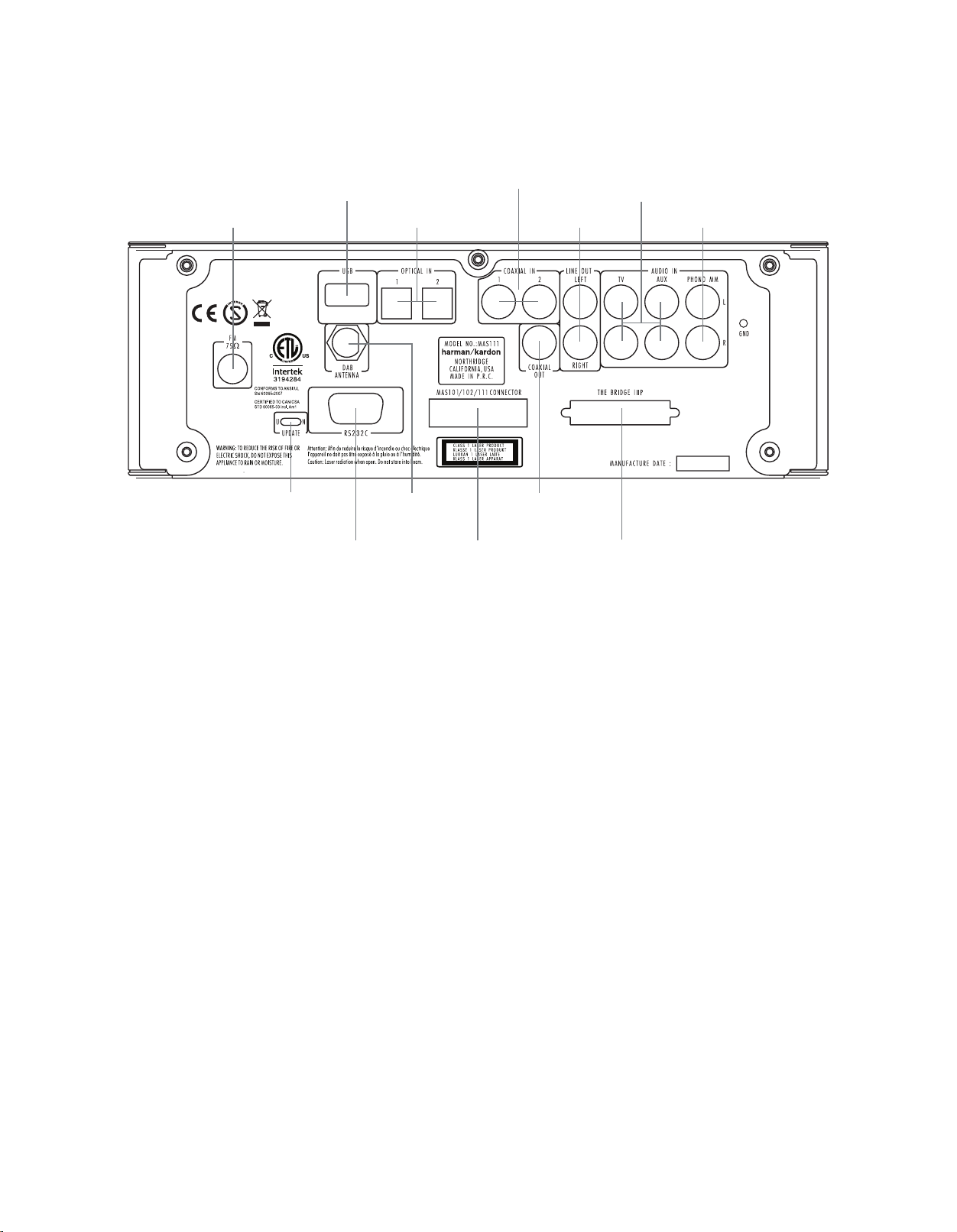
Rear-panel connections
Controller
c
a
l
k
0
FM Antenna Terminal: Connect the included FM antenna wire here.
1
DAB Antenna Terminal (MAS 111 Only): Connect the included DAB antenna wire
lead here to enjoy programm ing from digital DAB, DAB+ or T-DMB-Audio radio
stations available in your area.
2
USB Port B: Connect a compatible USB device here to enjoy playback of audio MP3
or WMA files. Although most USB flash and hard-disk drives in the FAT32 file format,
as well as many MP3 players, are compatible with the MAS system, due to the wide
variety of manufacturers, playback cannot be guaranteed. Do not connect an iPod
or iPhone to this port. Do not connect a personal computer or any peripherals to this
port.
3
Optic al 1/2 and Coaxial 1/2 Digital Audio Inputs: Connect a source device’s
optical or coaxial digital audio output to the corresponding input. Only the
uncompressed PCM format is supported.
4
T V and AUX Analog Audio Inputs: Connect the analog audio outputs of a tele-
vision or any source device to enjoy playback through the high-performance MAS
system.
5
Phono Input: Connect the outputs of a moving-magnet (MM) type turntable to this
input. Do not connect any other type of turntable to this input, and do not connect
the outputs of an MM-type turntable to any other analog audio inputs on the MAS
system without using a phono preamp, available separately from many electronics
stores.
6
The Bridge IIIP Input: To enjoy playback of audio materials stored on a compatible
iPod (see page 4), connect The Bridge IIIP. Make sure the insert for The Bridge IIIP is
installed, and install the appropriate dock adapter for your iPod within the insert, as
shown in Figure 1 on page 10.
d
b
d
h
i
j
7
Analog Audio O utputs: Connect these outputs to the analog audio inputs of an
audio recorder. When a source connected to the MAS system is playing, the signal will
be available at these outputs for recording. IMPORTANT: The Analog Audio Outputs
will mute when the Mute button on the remote is pressed. See page 9.
8
Coaxial Digital Audio O utput: Connect this output to the coaxial digital audio
input of a digital audio recorder. When the following sources are playing, the signal
will be available at this output for recording: CD, USB Ports A/B, Coaxial 1/2, Optical
1/2. The following sources are not available at this output: FM/DAB, TV, Aux, Phono,
The Bridge IIIP.
NOTES:
The MAS system can convert analog sources to the digital domain, or digital
•
sources to the analog domain for recording.
It is the user’s responsibility to comply with all laws pertaining to the
•
copying of audio materials.
9
O utput to Amplifier: Connect the incl uded ribbon cable to this connec tor and to
the corresponding connector on the MAS amplifier. This cable passes audio signals
from the controller to the amplifier, and it transfers DC power from the amplifier
to the controller. If this cable is ever damaged, do not use it, and contact Harman
Kardon for a replacement.
A
RS -232 Serial Port: This port is used only for system upgrades. Do not connect it to
any devices unless instructed to do so at the time a system upgrade is released.
B
Update Switch: This switch is used only for system upgrades. Leave it in the “N”
position for norm al operation unless instructed to sw itch it to the “U” pos ition to
install a system update.
e
f
g
Page 8
6
MAS SySteM
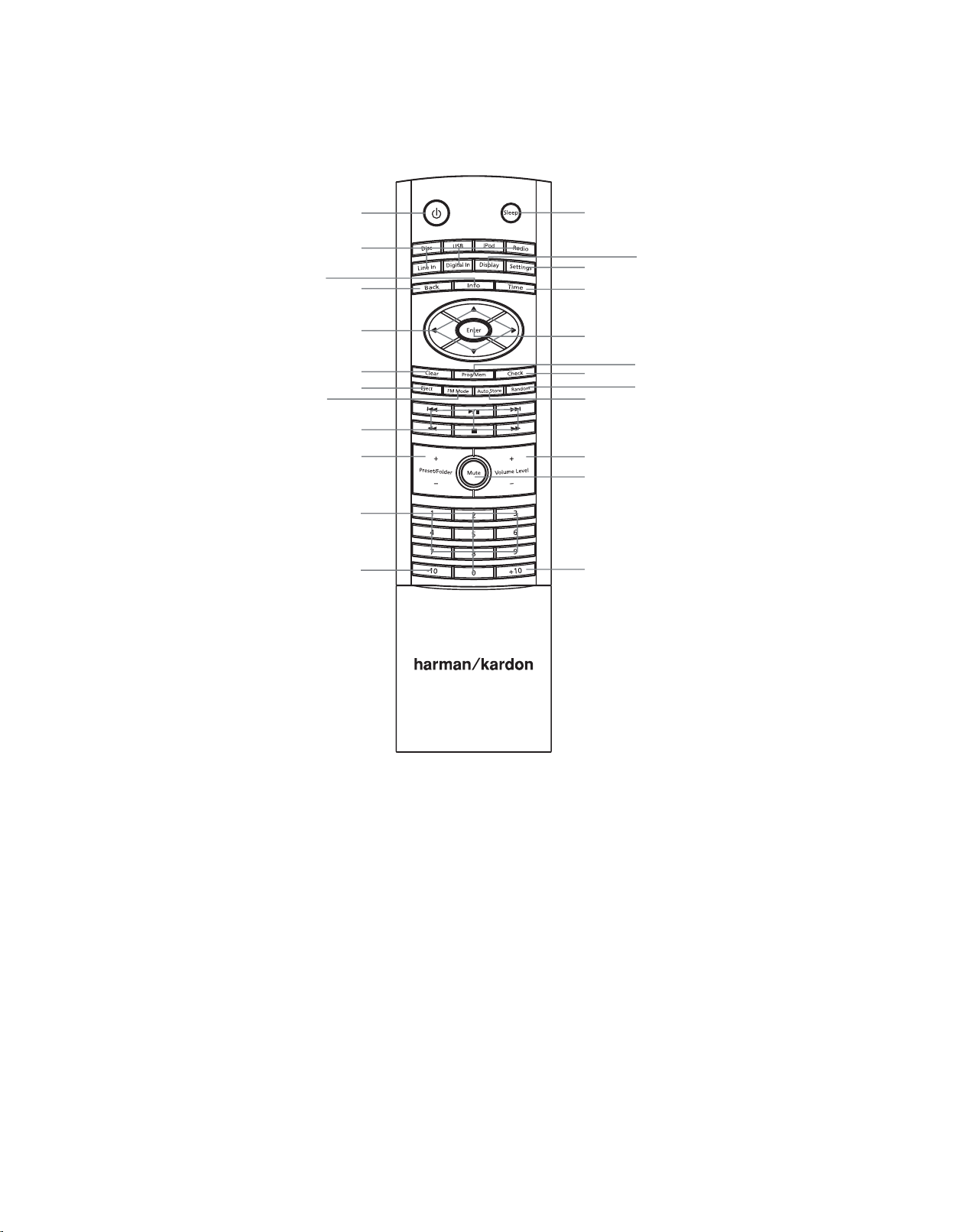
Remote control functions
Source Selectors
K/LM/N
FM Mode
Transport Controls
Preset/Folder +/–
–10 numeric Key
Power
Info
Back
Navigation
Clear
Eject
Numeric keys
Sleep
Settings
Time
Enter
Check
Auto Store
Volume +/–
Mute
+10 numeric Key
Display
Program/Memory
Random
Power: Turns the MAS system on or off. To completely power off the unit, unplug the
power supply.
Sleep: Each press increases the time until turn-off, from 10 to 90 minutes, in increments
of 10 minutes. The next press after the 90 minutes setting turns off the Sleep function.
Source Selectors: Selects a source input. Each press of the Line In or Digital In button
toggles among the available analog (L ine Input on right-side panel; TV, AUX or Phono
Input on rear panel) or digital audio inputs (Coaxial 1 or 2, Optical 1 or 2), respectively.
Press the iPod button to select an iPod docked in The Bridge IIIP.
Display: Adjusts the brightness of the message display. Each time the button is pressed
and held for one second, the message display brightness will cycle between full, half and
off. When the display is off while the system is turned on, the LEDs inside the Volume
knob and behind the front-panel function buttons will remain lit to remind you that the
system is still on.
Settings: Accesses menus for Speaker Setup (tone controls), Time Setup (clock), Alarm
Setup, System Version and System Reset. See the Operation section for more information.
Back: Returns to previous menu level.
Info: Displays the status of the current source:
Radio
•
: When FM band is in use, each press of the button toggles between the PS
(Program Service) and RT (Radio Text) RDS information, if available. When a DAB
radio station is playing (MAS 111 only), press this button to access the menu system
for the DAB tuner. See pages 13 and 14 for more information.
Audio CD
•
•
Time: Displays elapsed track time for the current Audio CD (no effect on data CDs or
other sources). Each additional press changes the display as follows: remaining track
time, elapsed disc time, remaining disc time then back to elapsed track time.
K/LM/N
through the Settin gs Menus, or through lists of content, and press the Enter button to
make selections. Press the Back button to return to the previous menu or content level.
Enter: Selects a menu item, or saves setting changes and returns to the previous menu
level.
: Displays CD Text information, if available. Each press of the button displays
the following items: Song, Artist, Album.
USB or Data CD
press of the button displays the individual items Song, Artist, Album, File type and
Folder, and then goes back to scrolling. If ID3 tags are not available, the file name will
appear.
: Scrolls all ID3 tag information for current source, if available. Each
Navigation buttons: Use the M and N buttons to scroll forward and reverse
Page 9

7
ENGLISH
MAS SySteM
Clear: Clears the current preset station or a playlist entry.
Radio
•
: To delete the current preset station, press the Clear button while it is playing.
Playlist
•
Program/Memory: Used to program playlists and radio presets.
•
•
Check: After a playlist has been programmed and play has been stopped, each press of
the Check button displays the tracks in the playlist.
Eject: When a CD is loaded, press this button to eject it.
FM Mode: Used with FM radio, each press toggles between Stereo and Monaural
playback.
Auto Store: Scans through all frequencies, searching for stations with acceptably strong
signal quality, and stores them as presets.
Random: Each press turns Random playback mode (shuffle) on or off. This mode plays
the tracks of the current disc or drive in random order.
: While programming a playlist, press the Clear button to delete the track just
entered. After the playlist has been saved by pressing the Stop button, press the Clear
button to delete the entire playlist. To delete a single track, stop play, press the Check
button repeatedly until the desired track appears and press the Clear button. Press
the Play or Stop button to exit the Check mode.
Radio
: If the current station has not been programmed into a preset, press Program/
Memory and press the Enter button to store the station at the current preset number,
or use the numeric keys to enter a different preset number. The new preset will
overwrite the existing one.
USB or CD (Audio or Data)
tracks to the playlist by using the Skip/Scan Transport Controls or the numeric keys
to select the t rack, then press the Program button to enter t he selection. Add up to
30 files. Press Play to play the playlist, or Stop to save the playlist without playing it.
During playback, the order of the track in the playlist will appear on the left, with the
disc’s track number to the right. See page 14 and 15.
: Press the Program button to begin Program Mode. Add
Remote control functions
Transport Controls
Track Skip Up/Down (iPod, CD or USB): Press and release the Next/Previous
skip buttons to skip to the next track, or the beginning of the current track. Press the
Previous Skip button twice to skip to the previous track.
Scan Forward/Reverse: These buttons function differently, depending on which
source has been selected:
iPod, CD or USB
•
track.
•
Radio:
by one increment/decrement. Press and hold a button to scan quickly through
the frequencies for next available station. Press the same button again to stop
scanning.
Play/Pause: Each tap toggles between the Play and Pause functions.
Stop: Fully stops playback.
Preset/Folder +/–: Selects a preset station or folder on a USB or data CD.
Radio
•
: Each press changes to the next or previous preset station, if any have been
programmed.
USB or Data CD
•
to the next or previous folder. After 3 seconds, the first track in the new folder will
begin playing.
Mute: Press to temporarily silence the speakers. Press again to restore audio. Muting is
also canceled if the MAS system is turned off.
NOTE: Pressing the Mute button also mutes the Analog Audio Outputs. See page 6.
Volume +/–: Increases or decreases the volume. Press and hold to change the volume
more quickly.
Numeric keys: Used to enter track numbers, radio stations or preset numbers, or while
adjusting the clock and alarm times.
–10 and +10 numeric Key: Used with a USB device or CD to quickly advance through a
large number of tracks. Each press of these keys changes to the next or previous track in
increments of 10.
: Press and hold a button to scan forward or reverse within a
Press and release a button to tune to the next higher or lower frequency
: Press once to open the current folder. Each additional press changes
Page 10
Line
8
Front
Panel
Control
Circuit
ConnectoionAmp
+5V
DGND
AGND
+3.3V
LDO
+1V
AMP_R-
AMP_L-
AMP_R+
AMP_L+
-15V
+15V
NJM
2608
Out_L
Out_R
+8V
MOLEX
IR
Sense
TOUCH
VFD
1
Sense
TOUCH
Driver
SPI
+5V
CPU
/SPI
2
I C
LDO
Out
Headphone
Out
Headphone
HP_Out_R
HP_Out_L
HP
AMP
Audio
Line
Line_Out_L
Out
Out
Line_Out_R
Subwoofer
Out
Subwoofer
Subwoofer_Out
Output
Main Digital
Coax
Out
SPDIF_SW
Coaxial_Out
1
2
3
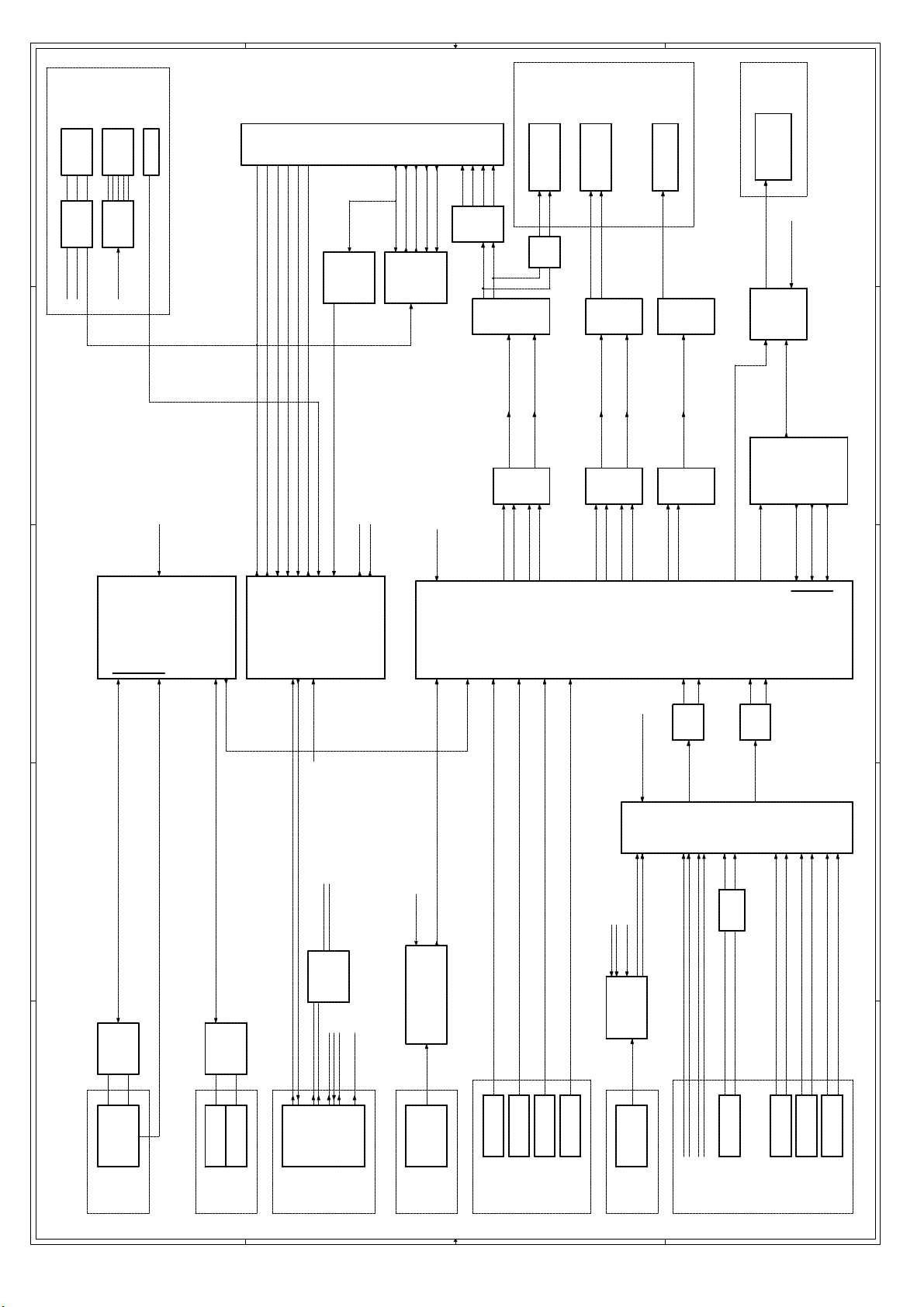
MAS111 Head Unit Block Diagram
Servo
Ali
SPI
M5673
USB 1.1
SPDIF_ALI_OUT
D/A
2
NJM
2608
Subwoofer_Out
NJM
2608
-
Dac3_L
AINL
+
-
2608
NJM
C
I
SPDIF_OUT_DIRECT
TXP
_Input_Out
SI
2
SAI
AINR
-
+
NJM
2608
SWITCH
74HC151
Tx
CS48540
_Iine_Out
S
2
I
DSP
_Main_Out
_Sub_Out
S
S
2
2
I
I
CX
2
3
Line_Out_L
++-
Dac2_L
NJM
NJM
2608
2608
+
Line_Out_R
-
Dac2_R
NJM
2608
Main_Out_R
Main_Out_L
Main_Out_R
Main_Out_L
NJM
2608
Relay_Control
Offset_detect
VOL-
VOL+
Mute_Audio
Standby
IR
Drop_detect
MM_MC_Sel
SPDIF_SW
Main
CPU
CI
2
+
-
Dac1_L
+
-
Dac1_R
CS42516
Spdif_In6
Spdif_In5
Spdif_In4
Spdif_In3
Spdif_In2
Spdif_In1
iPod CHECK
SPDIF_DAB_OUT
SPDIF_ALI_OUT
Coaxial_1
Coaxial_2
Optical_1
Optical_2
Line_In_1
Line_In_2
Line_In_3
BD3841FS
4
Line_In_4
Line_In_5
Line_In_6
Line_In_7
4
dB30
2
iPod_In-L
iPod_In-R
LMV
832
DRIVER
MOTOR
5
OPU
LOADER
SLOT IN
Disc
Drive
D D
RELAYUSB Front
USB Back
USB
Inputs
UART iPod TX
UART iPod RX
In-R
In-L
Charger GND
Charger +8V
iPod CHECK
HW Identification
iPod
Connector
iPod
C C
I C
C
2
I
Tuner_L
Tuner_R
SPI RDS
SPI Tuner
CAN
DAB/DAB+/DMB
Venice 7.1
Frontier Silicon
RF
Coax 2
Antenna
RF
DAB
RF
Coax 1
Digital
Optical 1
Inputs
B B
Optical 2
Tuner
RF_FM
iPod_In-R
RF
RF Antenna
RIAA
5
TV
Line
AUX
Line In
Inputs
A A
Jack_In_R
Jack_In_L
iPod_In-L
Phono MM
Page 11
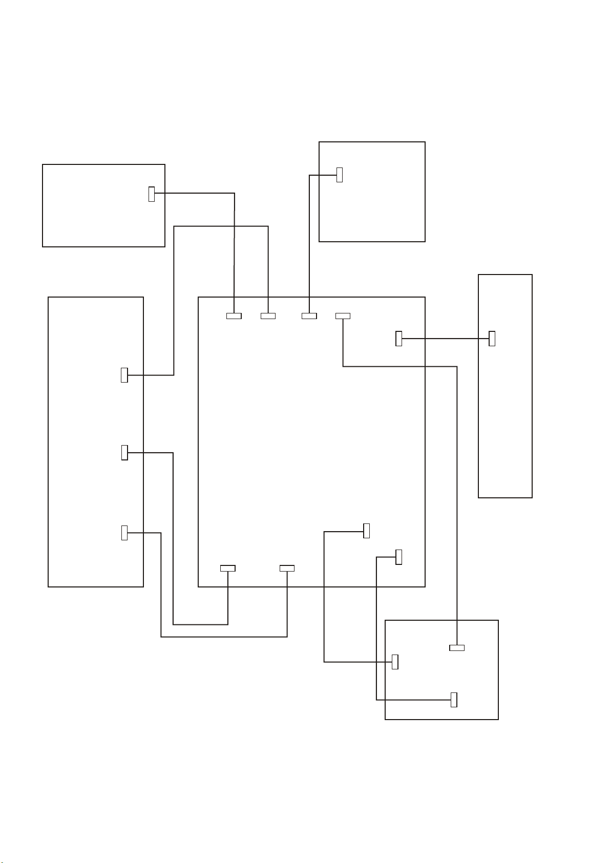
TUNER
9
WIRING DIAGRAM
BOARD
HEADPHONE
2P
CON8
16P
CN1
7P
CN1
RS232 BOARD
9P
CN2
10P
CN3
13P
CON1
9P
CON7
CON11
7P
CON5
CON10
10P
13P
6P
CON3
MAIN BOARD
CON9
16P
CON4
16P
DISPLAY BOARD
5P
CON2
CD CORE
Page 12
Philips Semiconductors Product specification
10
Hex inverter 74HCU04
FEATURES
• Output capability: standard
• ICC category: SSI
GENERAL DESCRIPTION
The 74HCU04 is a high-speed Si-gate CMOS device and is pin compatible with low power Schottky TTL (LSTTL).
It is specified in compliance with JEDEC standard no. 7A.
The 74HCU04 is a general purpose hex inverter. Each of the six inverters is a single stage
QUICK REFERENCE DATA
GND = 0 V; T
SYMBOL PARAMETER CONDITIONS TYP. UNIT
/ t
t
PHL
PLH
C
I
C
PD
=25°C; tr=tf=6ns
amb
propagation delay nA to nY CL= 15 pF; VCC=5V 5 ns
input capacitance 3.5 pF
power dissipation capacitance per inverter note 1 10 pF
Note
1. C
is used to determine the dynamic power dissipation (PD in µW):
PD
PD=CPD× V
2
× fi + ∑ (CL× V
CC
2
× fO) where:
CC
fi= input frequency in MHz
fo= output frequency in MHz
CL= output load capacitance in pF
VCC= supply voltage in V
∑ (CL× V
2
× fo) = sum of outputs
CC
ORDERING INFORMATION
“74HC/HCT/HCU/HCMOS Logic Package Information”
See
FUNCTION TABLE
INPUT OUTPUT
nA nY
L
H
H
L
Note
1. H = HIGH voltage level
L = LOW voltage level
.
Page 13
Philips Semiconductors Product specification
Hex inverter 74HCU04
PIN DESCRIPTION
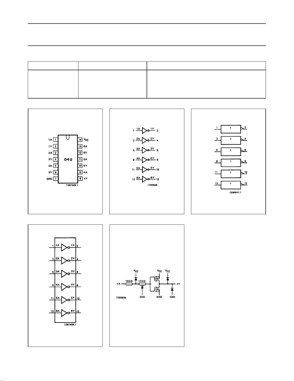
PIN NO. SYMBOL NAME AND FUNCTION
1, 3, 5, 9, 11, 13 1A to 6A data inputs
2, 4, 6, 8, 10, 12 1Y to 6Y data outputs
7 GND ground (0 V)
14 V
CC
positive supply voltage
Fig.1 Pin configuration. Fig.2 Logic symbol. Fig.3 IEC logic symbol.
Fig.4 Functional diagram.
Fig.5 Schematic diagram
(one inverter).
11
Page 14
12
Page 15
13
Page 16
14
Page 17
Features
• Low-voltage and Standard-voltage Operation
– 1.8 (V
= 1.8V to 5.5V)
CC
• Internally Organized 256 x 8 (2K)
• Two-wire Serial Interface
• Schmitt Trigger, Filtered Inputs for Noise Suppression
• Bidirectional Data Transfer Protocol
• 1 MHz (5V), 400 kHz (1.8V, 2.5V, 2.7V) Compatibility
• Write Protect Pin for Hardware Data Protection
• 8-byte Page (2K) Write Modes
• Partial Page Writes Allowed
• Self-timed Write Cycle (5 ms max)
• High-reliability
– Endurance: 1 Million Write Cycles
– Data Retention: 100 Years
• 8-lead PDIP, 8-lead JEDEC SOIC, 8-lead Ultra Thin Mini-MAP (MLP 2x3), 5-lead SOT23,
8-lead TSSOP and 8-ball dBGA2 Packages
• Lead-free/Halogen-free
• Available in Automotive
• Die Sales: Wafer Form, Tape and Reel and Bumped Wafers
Description
The AT24C02B provides 2048 bits of serial electrically erasable and programmable
read-only memory (EEPROM) organized as 256 words of 8 bits each. The device is
optimized for use in many industrial and commercial applications where low-power
and low-voltage operation are essential. The AT24C02B is available in space-saving
8-lead PDIP, 8-lead JEDEC SOIC, 8-lead Ultra Thin Mini-MAP (MLP 2x3)
SOT23, 8-lead TSSOP, and 8-ball dBGA2 packages and is accessed via a Two-wire
serial interface. In addition, the AT24C02B is available in 1.8V (1.8V to 5.5V) version.
, 5-lead
Two-wire
Serial EEPROM
2K (256 x 8)
AT24C02B
Table 0-1. Pin Configuration
Pin Name Function
A0 - A2 Address Inputs
SDA Serial Data
SCL Serial Clock Input
WP Write Protect
GND Ground
VCC Power Supply
Note: For use of 5-lead SOT23, the
software A2, A1, and A0 bits in
the device address word
must be set to zero to properly communicate.
8-lead Ultra-Thin
Mini-MAP (MLP 2x3)
VCC
WP
SCL
SDA
8
7
6
5
A0
1
A1
2
A2
3
GND
4
8-ball dBGA2
VCC
WP
SCL
SDA
Bottom View Bottom View
8-lead TSSOP
1
A0
2
A1
3
A2
GND
4
5-lead SOT23
SCL
GND
SDA
1
2
3
8
VCC
7
WP
6
SCL
5
SDA
WP
5
VCC
4
8-lead SOIC
A0
A1
A2
GND
8-lead PDIP
A0
A1
A2
GND
1
8
7
6
5
1
2
3
4
1
2
3
4
A0
2
A1
3
A2
4
GND
VCC
8
WP
7
SCL
6
SDA
5
8
VCC
7
WP
6
SCL
5
SDA
5126H–SEEPR–8/07
151718
Page 18
Page 19
Page 20
Page 21
CS42516
110 dB, 192 kHz 6-Ch Codec with S/PDIF Receiver
Features
Six 24-bit D/A, two 24-bit A/D Converters
110 dB DAC / 114 dB ADC Dynamic Range
-100 dB THD+N
System Sampling Rates up to 192 kHz
S/PDIF Receiver Compatible with EIAJ
CP1201 and IEC-60958
Recovered S/PDIF Clock or System Clock
Selection
8:2 S/PDIF Input MUX
ADC High-Pass Filter for DC Offset Calibration
Expandable ADC Channels and One-Line
Mode Support
Digital Output Volume Control with Soft Ramp
Digital +/-15 dB Input Gain Adjust for ADC
Differential Analog Architecture
Supports Logic Levels between 1.8 V and 5 V
General Description
The CS42516 codec provides two analog-to-di gital and
six digital-to-analog delta-sigma converters, as well as
an integrated S/PDIF receiver.
The CS42516 integrated S/PDIF receiver supports up
to eight inputs, clock recovery circuitry and format autodetection. The internal stereo ADC is capable of independent channel gain control for single-ended or
differential analog inputs. All six channels of DAC provide digital volume control and differential analog
outputs. The general-purpose outputs may be driven
high or low, or mapped to a variety of DAC mute controls or ADC overflow indicators.
The CS42516 is ideal for audio systems requiring wide
dynamic range, negligible distortion and low noise, such
as A/V receivers, DVD receivers, digital speaker and
automotive audio systems.
The CS42516 is available in a 64-pin LQFP package in
both Commercial (-10° to 70° C) and Automotive
(-40° to 85° C) grades. The CDB42518 Customer Demonstration board is also available for device evaluation.
Refer to “Ordering Information” on page 89.
RXP0
RXP1/GPO1
RXP2/GPO2
RXP3/GPO3
RXP4/GPO4
RXP5/GPO5
RXP6/GPO6
RXP7/GPO7
MUTEC
FILT+
VQ
REFGND
VA
AGND
AINL+
AINLAINR+
AINR-
AOUTA1+
AOUTA1-
AOUTB1+
AOUTB1-
AOUTA2+
AOUTA2-
AOUTB2+
AOUTB2-
AOUTA3+
AOUTA3-
AOUTB3+
AOUTB3-
Ref
Rx
GPO
MUTE
ADC#1
ADC#2
Analog Filter
VARX AGND
Clock/Data
Recovery
Digital Filter
Digital Filter
DAC#1
DAC#2
DAC#3
DAC#4
DAC#5
DAC#6
S/PDIF
Decoder
DEM
Gain & Clip
Gain & Clip
Digital Filter
DGND
C&U Bit
Data Buffer
Format
Detector
Internal MCLK
ADC
Serial
Data
DGND VDLPFLTTXP
VD
INT
Control
Port
Mult/Div
Serial
Audio
Interface
Port
CODEC
Serial
Port
Volume Control
RST
AD0/CS
AD1/CDIN
SDA/CDOUT
SCL/CCLK
VLC
OMCK
RMCK
SAI_LRCK
SAI_SCLK
SAI_SDOUT
VLS
ADCIN1
ADCIN2
CX_SDOUT
CX_LRCK
CX_SCLK
CX_SDIN1
CX_SDIN2
CX_SDIN3
http://www.cirrus.com
NOVEMBER '05
DS583F1
19
Page 22
2. PIN DESCRIPTIONS
VLS
CX_SDIN2
TEST
CX_SDIN3
SAI_SCLK
64 63 62 61 60 59 58 57 56 55 54 53 52 51 50 49
SAI_LRCK
OMCK
ADCIN1
SAI_SDOUT
RMCK
CX_SDOUT
ADCIN2
DGND
VD
TXP
CS42516
RXP0
VD
DGND
VLC
INT
RST
AINR-
AINR+
AINL+
AINL-
1
2
3
4
5
6
7
8
9
10
11
12
13
14
15
16
CX_SDIN1
CX_SCLK
CX_LRCK
SCL/CCLK
SDA/CDOUT
AD1/CDIN
AD0/CS
Pin Name # Pin Description
CX_SDIN1
CX_SDIN2
CX_SDIN3
CX_SCLK
CX_LRCK
VD
DGND
VLC
SCL/CCLK
SDA/CDOUT
AD1/CDIN
AD0/CS
1
Codec Serial Audio Data Input (Input) - Input for two’s complement serial audio data.
64
63
CODEC Serial Clock (Input/Output) - Serial clock for the CODEC serial audio interface.
2
CODEC Left Right Clock (Input/Output) - Determines which channel, Left or Right, is currently active on
3
the CODEC serial audio data line.
4
Digital Power (Input) - Positive power supply for the digital section.
51
5
Digital Ground (Input) - Ground reference. Should be connected to digital ground.
52
6
Control Port Power (Input) - Determines the required signal level for the control port.
Serial Control Port Clock (Input) - Serial clock for the serial control port. Requires an external pull-up
7
resistor to the logic interface voltage in I²C mode as shown in the Typical Connection Diagram.
Serial Control Data (Input/Output) - SDA is a data I/O line in I²C mode and requires an external pull-up
8
resistor to the logic interface voltage, as shown in the Typical Connection Diagram. CDOUT is the output
data line for the control port interface in SPI mode.
Address Bit 1 (I²C)/Serial Control Data (SPI) (Input) - AD1 is a chip address pin in I²C mode; CDIN is
9
the input data line for the control port interface in SPI mode.
Address Bit 0 (I²C)/Control Port Chip Select (SPI) (Input) - AD0 is a chip address pin in I²C mode; CS
10
is the chip select signal in SPI mode.
CS42516
17 18 19 20 21 22 23 24 25 26 27 2 8 29 30 31 32
VQ
NCNCNC
FILT+
REFGND
NC
VA
AGND
AOUTB3-
AOUTB3+
AOUTB2-
AOUTA3-
AOUTA3+
AOUTB2+
AOUTA2+
48
47
46
45
44
43
42
41
40
39
38
37
36
35
34
33
RXP1/GPO1
RXP2/GPO2
RXP3/GPO3
RXP4/GPO4
RXP5/GPO5
RXP6/GPO6
RXP7/GPO7
VARX
AGND
LPFLT
MUTEC
AOUTA1AOUTA1+
AOUTB1+
AOUTB1AOUTA2-
DS583F1
20
Page 23

INT
RST
AINR-
AINR+
AINL+
AINLVQ
FILT+
REFGND
NC
AOUTA1 +,AOUTB1 +,AOUTA2 +,AOUTB2 +,AOUTA3 +,AOUTB3 +,-
VA
VARX
AGND
MUTEC
LPFLT
RXP7/GPO7
RXP6/GPO6
RXP5/GPO5
RXP4/GPO4
RXP3/GPO3
RXP2/GPO2
RXP1/GPO1
RXP0
TXP
VLS
SAI_SDOUT
RMCK
CX_SDOUT
Interrupt (Output) - The CS42516 will generate an interrupt condition as per the Interrupt Mask register.
11
See “Interrupts” on page 40 for more details.
Reset (Input) - The device enters a low power mode and all internal registers are reset to their default
12
settings when low.
13
Differential Right Channel Analog Input (Input) - Signals are presented differentially to the delta-sigma
14
modulators via the AINR+/- pins.
15
Differential Left Channel Analog Input (Input) - Signals are presented differentially to the delta-sigma
16
modulators via the AINL+/- pins.
17
Quiescent Voltage (Output) - Filter connection for internal quiescent reference voltage.
18
Positive Voltage Reference (Output) - Positive reference voltage for the internal sampling circuits.
19
Reference Ground (Input) - Ground reference for the internal sampling circuits.
20
21
No Connect Pins - Do not make any connection to these pins.
22
23
36,37
35,34
32,33
Differential Analog Output (Output) - The full-scale differential analog output level is specified in the
31,30
Analog Characteristics specification table.
28,29
27,26
24
Analog Power (Input) - Positive power supply for the analog section.
41
25
Analog Ground (Input) - Ground reference. Should be connected to analog ground.
40
Mute Control (Output) - The Mute Control pin outputs high impedance following an initial power-on con-
dition or whenever the PDN bit is set to a ‘1’, forcing the codec into power-d own mode. The signal will
remain in a high impedance state as long as the part is in power-down mode. The Mute Control pin goes
38
to the selected “active” state during reset, muting, or if the master clock to left/right clock frequency ratio
is incorrect. This pin is intended to be used as a control for external mute circuits to prevent the clicks
and pops that can occur in any single supply system. The use of external mute circuits are not manda-
tory but may be desired for designs requiring the absolute minimum in extraneous clicks and pops.
39
PLL Loop Filter (Output) - An RC network should be connected between this pin and ground.
42
S/PDIF Receiver Input/ General Purpose Output (Input/Output) - Receiver inputs for S/PDIF encoded
43
data. The CS42516 has an internal 8:2 multiplexer to select the active receiver port, according to the
44
Receiver Mode Control 2 register. These pins can also be configured as general purpose output pins,
45
ADC Overflow indicators or Mute Control outputs accor din g to the RXP/Ge n eral Purp o se Pin C ontro l
46
registers.
47
48
S/PDIF Receiver Input (Input) - Dedicated receiver input for S/PDIF encoded data.
49
S/PDIF Transmitter Output (Output) - S/PDIF encoded data output, mapped directly from one of the
50
receiver inputs as indicated by the Receiver Mode Control 2 register.
53
Serial Port Interface Power (Input) - Determines the required signal level for the serial port interfaces.
Serial Audio Interface Serial Data Output (Output) - Output for two’s complement serial audio PCM
54
data from the S/PDIF incoming stream. This pin can also be configured to transmit the output of the inter-
nal and external ADCs.
Recovered Master Clock (Output) - Recovered master clock output from the External Clock Reference
55
(OMCK, pin 59) or the PLL which is locked to the incoming S/PDIF stream or CX_LRCK.
CODEC Serial Data Output (Output) - Output for two’s complement serial audio data from the internal
56
and external ADCs.
CS42516
DS583F1
21
Page 24

ADCIN1
ADCIN2
OMCK
TEST
SAI_LRCK
SAI_SCLK
CS42516
External ADC Serial Input (Input) - The CS42516 provides for up to two external stereo analog to digital
58
converter inputs to provide a maximum of six channels on one serial data output line when the CS42516
57
is placed in One-Line Mode.
External Reference Clock (Input) - External clock reference that must be within the ranges specified in
59
the register “OMCK Frequency (OMCK Freqx)” on page 53.
62
Test Pin (Input) - This pin must be connected to DGND.
Serial Audio Interface Left/Right Clock (Input/Output) - Determines which channel, Left or Right, is
60
currently active on the serial audio data line.
Serial Audio Interface Serial Clock (Input/Output) - Serial clock for the Serial Audio Interface.
61
DS583F1
22
Page 25
3. TYPICAL CONNECTION DIAGRAM
CS42516
+3.3 V to +5 V
+2.5 V
to + 5 V
+1.8 V
to + 5 V
** Resistors are required for
10 µF
10 µF
Driver
S/PDIF
Inte rfa c e
Up to 8
Sources
CS5361
A/D Converter
CS5361
A/D Converter
Digital Audio
Processor
Micro-
Controller
2
C control port operation
I
0.1 µF 0.01 µF
+
0.1 µF
+
OSC
** **
2 kΩ 2 kΩ
0.01 µF
0.1 µF
0.1 µF
50
49
48
47
46
45
44
43
42
53
59
58
57
55
54
60
61
3
2
56
1
64
63
11
12
7
8
9
10
6
62
4
VD
TXP
RXP0
RXP1/GPO1
RXP2/GPO2
RXP3/GPO3
RXP4/GPO4
RXP5/GPO5
RXP6/GPO6
RXP7/GPO7
VLS
OMCK
ADCIN1
ADCIN2
RMCK
51
CS42516
SAI_SDOUT
SAI_LRCK
SAI_SCLK
CX_LRCK
CX_SCLK
CX_SDOUT
CX_SDIN1
CX_SDIN2
CX_SDIN3
INT
RST
SCL/CCLK
SDA/CDOUT
AD1/CDIN
AD0/CS
VLC
TEST
DGND
DGND
52 40
5
25
41
VAVD
24
VA
AOUTA1+
AOUTA1-
AOUTB1+
AOUTB1-
AOUTA2+
AOUTA2-
AOUTB2+
AOUTB2-
AOUTA3+
AOUTA3-
AOUTB3+
AOUTB3-
MUTEC
AINL+
AINL-
AINR+
AINR-
VQ
FILT+
REFGND
LPFLT
AGNDAGND
0.01 µF
0.01 µF
36
37
35
34
32
33
31
30
28
29
27
26
+VA
38
15
16
14
13
17
18
19
39
*
*
0.1 µF
RFILT
CFILT
0.1 µF
+
10 µF
0.1 µF
+
10 µF
Analog Output Buffer
and
Mute Circuit (optional)
Analog Output Buffer
and
Mute Circuit (optional)
Analog Output Buffer
and
Mute Circuit (optional)
Analog Output Buffer
and
Mute Circuit (optional)
Analog Output Buffer
and
Mute Circuit (optional)
Analog Output Buffer
and
Mute Circuit (optional)
Mute
Drive
(optional)
* Pull up or down as
required on startup if the
M u te C o n tro l is u s e d .
Analog
2700 pF*
Input
1
Buffer
Analog
Input
2700 pF*
1
Buffer
+
100 µF
3
3
CRIP
0.1 µF
3
+5 V
2
2
2
2
2
2
Left Analog Input
Right Analog Input
+
4.7 µF
DS583F1
Connect DGN D and A G ND at single point near Codec
1. See the ADC Input Filter section in the Appendix.
2. See the DAC O utput Filter section in the Appendix.
3. See the PLL Filter section in the Appendix.
Figure 5. Typical Connection Diagram
23
Page 26
CS485xx Family Data Sheet
FEATURES
Cost-effective, High-performance 32-bit DSP
— 300,000,000 MAC/S (multiply accumulates per second)
— Dual MAC cycles per clock
— 72-bit accumulators are the most accurate in the industry
— 24k x 32 SRAM, 2k blocks - assignable to data or program
— Internal ROM contains a variety of configurable sound
enhancement feature sets
— 8-channel internal DMA
— Internal watch-dog DSP lock-up prevention
DSP Tool Set w/ Private Keys for Protecting Customer IP
Configurable Serial Audio Inputs/Outputs
— Configurable for all input/output types
— Maximum 32-bit @ 192 kHz
— Supports 32-bit audio sample I/O between DSP chips
— TDM input modes (multiple channels on same line)
— 192 k Hz SP DIF transmitter
— Multi-channel DSD direct stream digital SACD input
Supports Two Diff eren t Input Fs Sam ple Rates
— Output can be master or slave
— Dual processing path capability
— Input supports dual domain slave clocking
— Hardware assist time sampling for sample rate conversion
Integrated Clock Manager/PLL
— Can operate from external crystal, external oscillator
Input Fs Auto Detection
Host & Boot via Serial Interface
Configurable GPIOs and External Interrupt Input
1.8V Core and a 3.3V I/O that is tolerant to 5V input
Low-power Mode
— “Energy-Star Ready” via low-power mode, 268 µW in
standby
Differentiating from the legacy Cirrus multi-standard, multichannel decoders, this new CS485xx family is still based on
the same high-performance 32-bit fixed point Digital Signal
Processor core but instead is equipped with much less
memory, tailoring it for more cost-effective applications
associated with multi-channel and virtual-channel sound
enhancements. Target applications are:
— Digital Televisions
— Multimedia Peripherals
—iPod
— Automotive Head Units
— Automotive Outboard Amplifiers
— HD-DVD & Blu-ray Disc DVD Receivers
— PC Speakers
There are are also a wide variety of licensable DSP codes
available today as seen by the following examples:
Cirrus also ha s developed, or is developing their own royal tyfree versions of popular features sets like Cirrus Bass
Manager, Cirrus Dynamic Volume Leveler, Cirrus Original
Multichannel Surround, Cirrus Virtual Speaker & Cirrus 3DAudio.
The CS485xx family is programmed using the Cirrus
proprietary DSP Composer
Processing chains may be designed using a drag-and-drop
interface to place/utilize functional macro audio DSP
primitives. The end result is a software image that is downloaded to the DSP via serial host or serial boot modes.
Ordering Information:
See page 20 for ordering information
®
Docking Stations
L
A
FT
DRA
™
GUI development tool.
®
DELPHI
D
M
A
GPIO Debug
12 Ch. Audio In /
6 Ch. SACD In
S/PDIF
12 Ch PCM
Audio Out
Serial
Control 1
32-bit
DSP
P X Y
CONFIDENTI
http://www.cirrus.com
24
Watchdog
TMR1
TMR2
PLL
Page 27
8.2 CS48540, 48-pin LQFP Pinout Diagram
GPIO10, SCP__MISO / SDA
GPIO9, SCP_MOSI
GND4
GPIO7, HS4
33
32
VDDIO3
37
GPIO11, SCP_CLK
36
35
34
GPIO6, DAO2_DATA0, HS3
31
CS485xx Family Data Sheet
32-bit Audio Decoder DSP Family
GPIO3, DAO1_ DATA1, HS1
VDD2GND2
GPIO5, XMTA
GNDIO3
30
28
29
GPIO4, DAO1_ DATA2, HS2
GPIO18, DAO_MCLK
26
27
25
VDDIO2
24
GPIO8, SCP_CS#
GPOI12, SCP_IRQ#
GNDIO4
GPIO13, SCP_BSY#, EE_CS#
VDD3
XTAL_OUT GPIO15, DAI2_SCLK
XTO
GNDA
PLL_REF_RES
VDDA (3.3V)
38
39
40
23
22
21
DAO_SCLK
GND3
DAO_LRCLK
FT
41
42
43
CS48540
48-Pin LQFP
DAO1_DATA0, HS0
20
19
GNDIO2
18
DRA
XTI
44
45
46
47
48
1
2
3
4
5
6
7
L
A
8
HI
9
10
11
GPIO14, DAI2_LRCLK
17
16
VDD1
GPIO17,
15
14
GPIO2
GPIO1, DAI1_DATA2
13
12
DAI2_DATA0
TEST
DBDA
RESET#
GND1
DBCK
GNDIO1
DAI1_LRCLK
DAI1_SCLK
DELP
GPIO16, DAI1_DATA0
GPIO0, DAI1_DATA1
Figure 12. CS48540, 48-Pin LQFP Pinout
CONFIDENTI
VDDIO1
25
Page 28
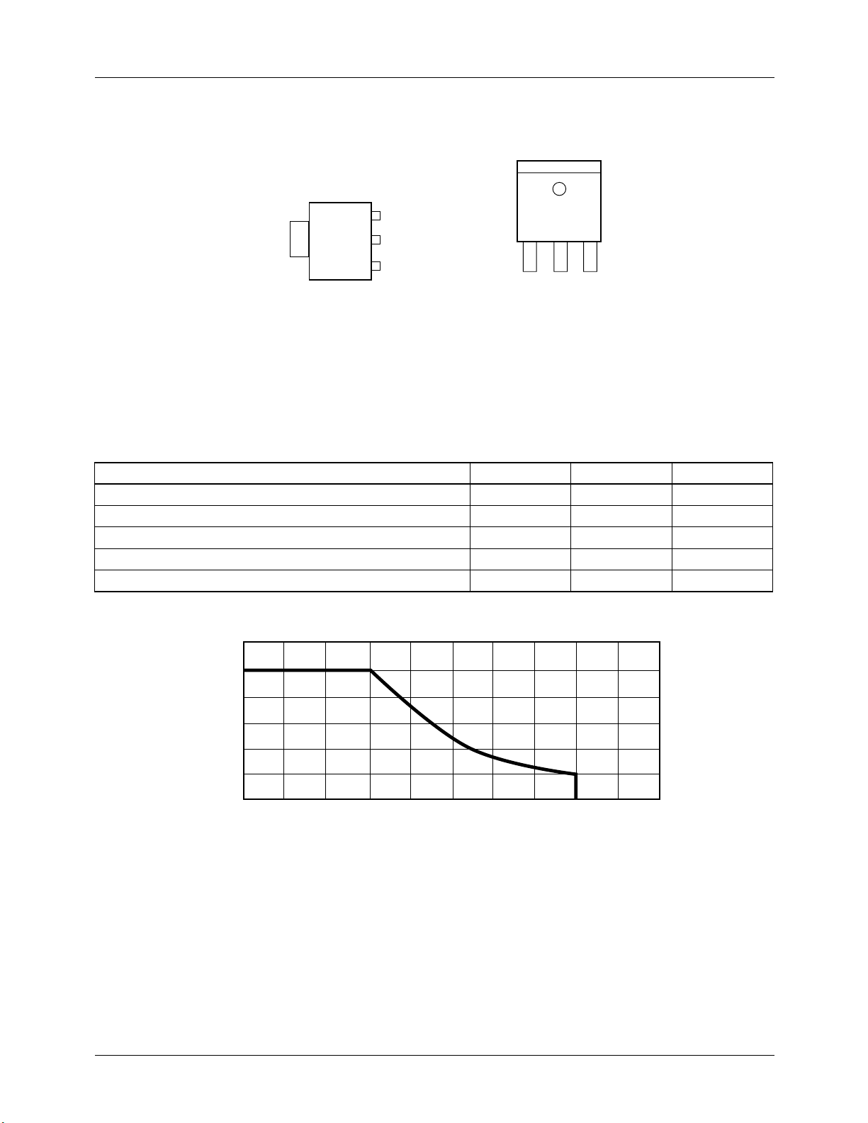
FAN1112
1A 1.2V Low Dropout Linear Regulator
Features
• Low dropout voltage
• Load regulation: 0.05% typical
• Trimmed current limit
• On-chip thermal limiting
• Standard SOT-223 and TO-252 packages
• Three-terminal fixed 1.2V
Applications
• Post regulator for switching supplies
• Supply for low-voltage processors
Typical Application
Description
The FAN1112 is a 1.2V low dropout three-terminal
regulator with 1A output current capability. The device has
been optimized for low voltage where transient response and
minimum input voltage are critical.
Current limit is trimmed to ensure specified output current
and controlled short-circuit current. On-chip thermal limiting
provides protection against any combination of overload and
ambient temperatures that would create excessive junction
temperatures.
Unlike PNP type regulators where up to 10% of the output
current is wasted as quiescent current, the quiescent current
of the FAN1112 flows into the load, increasing efficiency.
The FAN1112 regulator is available in the industry-standard
SOT-223 and TO-252 (DPAK) power packages.
FAN1112
V
= 3.3V V
IN
10µF
++
GND
V
OUT
IN
1.2V at 1A
22µF
26
Page 29
°
°
°
Pin Assignments
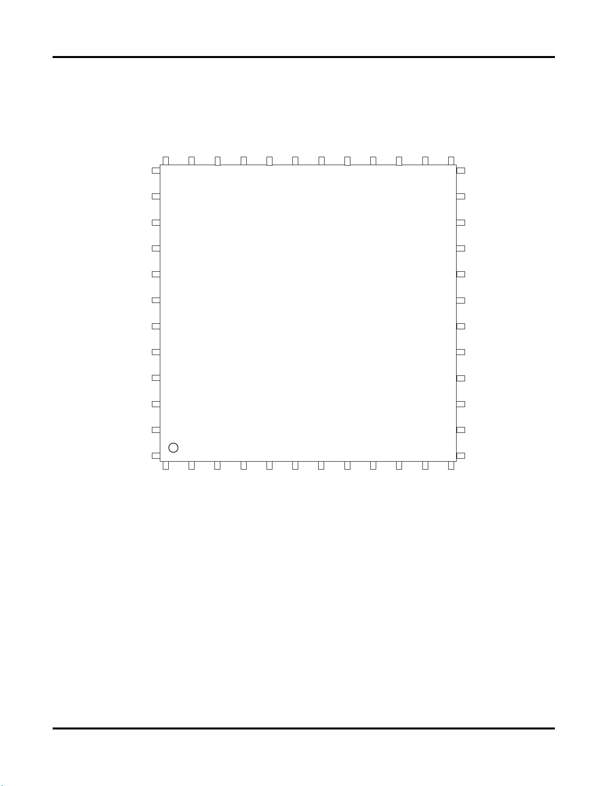
Tab is
V
OUT
Front View
Front View
Tab is V
OUT
3
IN
1
2
OUT
1
GND
GND OUT IN
23
4-Lead Plastic SOT-223
Θ
= 15°C/W*
JC
*With package soldered to 0.5 square inch copper area over backside ground plane or internal power plane., Θ
3-Lead Plastic TO-252
ΘJC = 3°C/W*
can vary from
JA
30°C/W to more than 50°C/W. Other mounting techniques may provide better thermal resistance than 30°C/W.
Absolute Maximum Ratings
Parameter Min. Max. Unit
V
IN
(V
IN
– V
OUT
) * I
OUT
Operating Junction Temperature Range 0 125
Storage Temperature Range -65 150
Lead Temperature (Soldering, 10 sec.) 300
1.2
1.0
0.8
(A)
0.6
OUT
I
0.4
18 V
See Figure 1
C
C
C
0.2
0
068
10 12 14 16 18 2042
V
– V
OUT
(V)
IN
Figure 1. Absolute Maximum Safe Operating Area
27
Page 30

HEF4094B
8-stage shift-and-store register
Rev. 08 — 2 April 2010 Product data sheet
1. General description
The HEF4094B is an 8-stage serial shift register. It has a storage latch associated with
each stage for strobing data from the serial input to par allel buffered 3-state outputs
QP0 to QP7. The parallel outputs may be connected directly to common bus lines. Data is
shifted on positive-going clock transitions. The data in each shift register stage is
transferred to the storage register when the strobe (STR) input is HIGH. Data in the
storage register appears at the outputs whenever the output enable (OE) signal is HIGH.
Two serial ou tputs (QS1 and QS2) are available for cascading a number of HEF4094B
devices. Serial data is available at QS1 on positive -going clock e dges to allow high -speed
operation in cascaded systems with a fast clock rise time. The same seri al data is
available at QS2 on the next negative going clock edge. This is used for cascading
HEF4094B devices when the clock has a slow rise time.
It operates over a recommended V
(usually ground). Unused inputs must be connected to V
also suitable for use over the industrial (−40 °C to +85 °C) and automotive (−40 °Cto
+125 °C) temperature ranges.
power supply range of 3 V to 15 V referenced to VSS
DD
, VSS, or another input. It is
DD
2. Features and benefits
Fully static operation
5 V, 10 V, and 15 V parametric ratings
Standardized symmetrical output characteristics
Operates across the automotive temperature range −40 °C to +125 °C
Complies with JEDEC standard JESD 13-B
3. Ordering information
Table 1. Ordering information
All types operate from
Type number Package
HEF4094BP DIP16 plastic dual in-line package; 16 leads (300 mil) SOT38-4
HEF4094BT SO16 plastic small outline package; 16 leads; body width 3.9 mm SOT109-1
HEF4094BTS SSOP16 plastic shrink small outline package; 16 leads; body width 5.3 mm SOT338-1
−40°
C to +125°C.
Name Description Version
28
Page 31

NXP Semiconductors
001aaf119
001aaf111
4. Functional diagram
D
2
CP
3
STR
1
OE
15
QP0
8-STAGE SHIFT
REGISTER
8-BIT STORAGE
REGISTER
3-STATE OUTPUTS
QP1 QP2 QP3 QP4 QP5 QP6 QP7
QS2
QS1
HEF4094B
8-stage shift-and-store register
31
CP STR
QS1
QS2910
QP0
10
9
2OED
QP1
QP2
QP3
QP4
QP5
QP6
QP7
4
5
6
7
14
13
12
11
4 5 6 7 14 13 12 11
Fig 1. Functional diagram Fig 2. Logic symbol
STAGES 1 TO 6STAGE 0 STAGE 7
CP
STR
OE
DD
CP
FF 0
DLEQ
LATCH 0
Q
QP0
D
CP
QP1
QP2
QP3
QP4
QP5
QP6
Q
DCPQ
FF 7
DLEQ
LATCH 7
QP7
15
D QS2
Q
LE
LATCH
001aag799
QS1
Fig 3. Logic diagram
29
Page 32

NXP Semiconductors
5. Pinning information
5.1 Pinning
HEF4094B
8-stage shift-and-store register
HEF4094B
1
STR V
2
DOE
3
CP QP4
4
QP0 QP5
5
QP1 QP6
6
QP2 QP7
7
QP3 QS2
8
V
SS
001aae662
Fig 4. Pin configuration
5.2 Pin description
Table 2. Pin description
Symbol Pin Description
STR 1 strobe input
D 2 data input
CP 3 clock input
QP0 to QP7 4, 5, 6, 7, 14, 13, 12, 11 parallel output
V
SS
QS1 9 serial output
QS2 10 serial output
OE 15 output enable input
V
DD
8 ground supply voltage
16 supply voltage
16
DD
15
14
13
12
11
10
9
QS1
30
Page 33

NXP Semiconductors
001aaf117
HEF4094B
8-stage shift-and-store register
6. Functional description
Table 3. Function table
Inputs Parallel outputs Serial outputs
CP OE STR D QP0 QPn QS1 QS2
↑ LXXZZQ6SNC
↓ LXXZZNCQ7S
↑ HLXNCNCQ6SNC
↑ HHLL QPn −1Q6S NC
↑ HHHHQPn −1Q6S NC
↓ H H H NCNCNCQ7S
[1] At the positive clock edge, the information in the 7th register stage is transferred to the 8th register stage and the QSn outputs.
H = HIGH voltage level; L = LOW voltage level; X = don’t care;
↑ = positive-going transition; ↓ = negative-going transition;
Z = HIGH-impedance OFF-state; NC = no change;
Q6S = the data in register stage 6 before the LOW to HIGH clock transition;
Q7S = the data in register stage 7 before the HIGH to LOW clock transition.
[1]
CLOCK INPUT
STROBE INPUT
OUTPUT ENABLE INPUT
INTERNAL Q0S (FF 0)
INTERNAL Q6S (FF 6)
SERIAL OUTPUT QS1
SERIAL OUTPUT QS2
Fig 5. Timing diagram
DATA INPUT
OUTPUT QP0
OUTPUT QP6
Z-state
Z-state
31
Page 34

Features
·
Operating voltage: 2.0V~5.5V
·
Maximum input serial clock: 500kHz at VDD=2V,
2MHz at V
·
Operating current: less than 1mAat2V,
DD
=5V
less than 1.2mAat5V
·
TTL compatible
-
VIH: 2.0V~VDD+0.3V at VDD=5V
-
VIL: -0.3V~+0.8V at VDD=5V
Applications
·
Microcomputer serial clock
General Description
The HT1380/HT1381 is a serial timekeeper IC which
providesseconds,minutes,hours,day,date,monthand
year information. The number of days in each month
and leap years are automatically adjusted. The
HT1380/HT1381 is designed for low power consumption and can operate in two modes: one is the 12-hour
mode with an AM/PM indicator, the other is the 24-hour
mode.
HT1380/HT1381
Serial Timekeeper Chip
·
Two data transmission modes: single-byte,
or burst mode
·
Serial I/O transmission
·
All registers store BCD format
·
HT1380: 8-pin DIP package
HT1381: 8-pin SOP package
·
Clock and Calendar
The HT1380/HT1381 has several registers to store the
corresponding information with 8-bit data format. A
32768Hz crystal is required to provide the correct timing. In order to minimize the pin number, the
HT1380/HT1381 use a serial I/O transmission method
to interface with a microprocessor. Only three wires are
required: (1) REST
delivered 1 byte at a time or in a burst of up to 8 bytes.
, (2) SCLK and (3) I/O. Data can be
Block Diagram
Pin Assignment
S C L K
R E S T
N C
X 1
X 2
V S S
I / O
1
2
3
4
H T 1 3 8 0
8 D I P - A
D a t a S h i f t
R e g i s t e r
C o m m a n d
C o n t r o l L o g i c
V D D
8
7
S C L K
I / O
6
R E S T
5
R e a l T i m e
C l o c k
O s c i l l a t o r a n d
D i v i d e r C i r c u i t
1
N C
2
X 1
3
X 2
4
V S S
H T 1 3 8 1
8 S O P - A
X 1
X 2
V D D
8
7
S C L K
I / O
6
R E S T
5
9
32
Page 35

Pad Assignment
1
2
3
4
5
6
7
( 0 , 0 )
X 1
X 2
V S S
I / O
S C L K
V D D
R E S T
HT1380/HT1381
Chip size: 2010 ´ 1920 (mm)
2
* The IC substrate should be connected to VSS in the PCB layout artwork.
Pad Coordinates
Pad No. X Y
1
2
3
-851.40
-851.40
-844.40 -203.90
4 845.90
5 848.40
6 845.90 332.60
7 844.40 572.60
Pad Description
Pad No. Pad Name I/O
1 X1 I CMOS 32768Hz crystal input pad
2 X2 O CMOS Oscillator output pad
3 VSS
4 REST
¾
I CMOS Reset pin with serial transmission
5 I/O I/O CMOS Data input/output pin with serial transmission
6 SCLK I CMOS Serial clock pulse pin with serial transmission
7 VDD
¾
Internal
Connection
Description
CMOS Negative power supply, ground
CMOS Positive power supply
Unit: mm
775.00
494.60
-618.30
-4.30
33
Page 36

LM117/LM317A/LM317
3-Terminal Adjustable Regulator
General Description
The LM117 series of adjustable 3-terminal positive voltage
regulators is capable of supplying in excess of 1.5A over a
1.2V to 37V output range. They are exceptionally easy to
use and require only two external resistors to set the output
voltage. Further,both line and load regulation are better than
standard fixed regulators. Also, the LM117 is packaged in
standard transistor packages which are easily mounted and
handled.
In addition to higher performance than fixed regulators, the
LM117 series offers full overload protection available only in
IC’s. Included on the chip are current limit, thermal overload
protection and safe area protection. All overload protection
circuitry remains fully functional even if the adjustment terminal is disconnected.
Normally,no capacitors are needed unless the device is situated more than 6 inches from the input filter capacitors in
which case an input bypass is needed. An optional output
capacitor can be added to improve transient response. The
adjustment terminal can be bypassed to achieve very high
ripple rejection ratios which are difficult to achieve with standard 3-terminal regulators.
Besides replacing fixed regulators, the LM117 is useful in a
wide variety of other applications. Since the regulator is
“floating” and sees only the input-to-output differential volt-
age, supplies of several hundred volts can be regulated as
long as the maximum input to output differential is not exceeded, i.e., avoid short-circuiting the output.
Also, it makes an especially simple adjustable switching
regulator,a programmable output regulator, or by connecting
a fixed resistor between the adjustment pin and output, the
LM117 can be used as a precision current regulator. Supplies with electronic shutdown can be achieved by clamping
the adjustment terminal to ground which programs the output to 1.2V where most loads draw little current.
For applications requiring greater output current, see LM150
series (3A) and LM138 series (5A) data sheets. For the
negative complement, see LM137 series data sheet.
Features
n Guaranteed 1%output voltage tolerance (LM317A)
n Guaranteed max. 0.01%/V line regulation (LM317A)
n Guaranteed max. 0.3%load regulation (LM117)
n Guaranteed 1.5A output current
n Adjustable output down to 1.2V
n Current limit constant with temperature
n P
n 80 dB ripple rejection
n Output is short-circuit protected
+
Product Enhancement tested
LM117/LM317A/LM317 3-Terminal Adjustable Regulator
August 1999
Typical Applications LM117 Series Packages
1.2V–25V Adjustable Regulator
Full output current not available at high input-output voltages
*
Needed if device is more than 6 inches from filter capacitors.
†
Optional— improves transient response. Output capacitors in the range
of 1 µF to 1000 µF of aluminum or tantalum electrolytic are commonly
used to provide improved output impedance and rejection of transients.
DS009063-1
Part Number Design
Suffix Package Load
Current
K TO-3 1.5A
H TO-39 0.5A
T TO-220 1.5A
E LCC 0.5A
S TO-263 1.5A
EMP SOT-223 1A
MDT TO-252 0.5A
SOT-223 vs D-Pak (TO-252)
Packages
Scale 1:1
DS009063-54
34
Page 37

LM9022
Vacuum Fluorescent Display Filament Driver
LM9022 Vacuum Fluorescent Display Filament Driver
August 2005
General Description
The LM9022 is a bridged power amplifier capable of delivering typically 2W of continuous average power into a 10Ω
filament load when powered by a 5V power supply.
To conserve power in portable applications, the LM9022’s
micropower shutdown mode (I
when V
Additional LM9022 features include thermal shutdown protection, unity-gain stability, and external gain set.
is applied to the SHUTDOWN pin.
DD
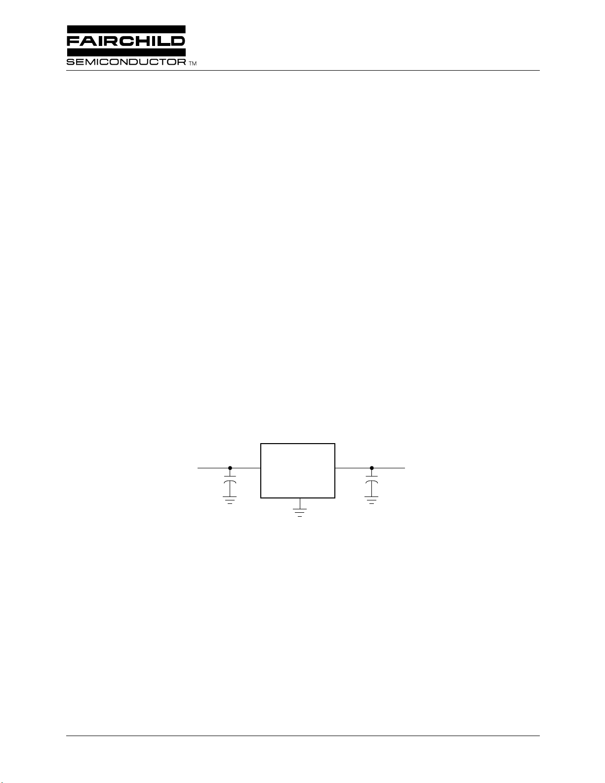
Typical Application T
= 0.6µA, typ) is activated
Q
= 25˚C, VDD= 5V, unless otherwise specified.
A
Key Specifications
n IDDduring shutdown 0.6µA (typ)
n Thermal Shutdown Protection
Features
n No transformers required
n SO or DIP packaging
Applications
n VCR/DVD Displays
n RADIO/TUNER Displays
Connection Diagram
20021501
FIGURE 1. Typical Application Circuit
MSOP, Small Outline, and DIP Package
20021502
Top View
Order Number LM9022M or LM9022N
See NS Package Number M08A or N08E
35
Page 38

October 6, 2008
LMV831 Single/ LMV832 Dual/ LMV834 Quad
3.3 MHz Low Power CMOS, EMI Hardened Operational
Amplifiers
General Description
National’s LMV831, LMV832, and LMV834 are CMOS input,
low power op amp IC's, providing a low input bias current, a
wide temperature range of −40°C to 125°C and exceptional
performance making them robust general purpose parts. Additionally, the LMV831/LMV832/LMV834 are EMI hardened
to minimize any interference so they are ideal for EMI sensitive applications.
The unity gain stable LMV831/LMV832/LMV834 feature
3.3 MHz of bandwidth while consuming only 0.24 mA of current per channel. These parts also maintain stability for capacitive loads as large as 200 pF. The LMV831/LMV832/
LMV834 provide superior performance and economy in terms
of power and space usage.
This family of parts has a maximum input offset voltage of
1 mV, a rail-to-rail output stage and an input common-mode
voltage range that includes ground. Over an operating range
from 2.7V to 5.5V the LMV831/LMV832/LMV834 provide a
PSRR of 93 dB, and a CMRR of 91 dB. The LMV831 is offered
in the space saving 5-Pin SC70 package, the LMV832 in the
8-Pin MSOP and the LMV834 is offered in the 14-Pin TSSOP
package.
Features
Unless otherwise noted, typical values at TA= 25°C,
V+ = 3.3V
■
Supply voltage 2.7V to 5.5V
■
Supply current (per channel) 240 µA
■
Input offset voltage 1 mV max
■
Input bias current 0.1 pA
■
GBW 3.3 MHz
■
EMIRR at 1.8 GHz 120 dB
■
Input noise voltage at 1 kHz 12 nV/√Hz
■
Slew rate 2 V/µs
■
Output voltage swing Rail-to-Rail
■
Output current drive 30 mA
■
Operating ambient temperature range −40°C to 125°C
Applications
■
Photodiode preamp
■
Piezoelectric sensors
■
Portable/battery-powered electronic equipment
■
Filters/buffers
■
PDAs/phone accessories
Typical Application
EMI Hardened Sensor Application
30024101
LMV831 Single/ LMV832 Dual/ LMV834 Quad 3.3 MHz Low Power CMOS, EMI Hardened
Operational Amplifiers
36
Page 39

Absolute Maximum Ratings (Note 1)
If Military/Aerospace specified devices are required,
please contact the National Semiconductor Sales Office/
Distributors for availability and specifications.
ESD Tolerance (Note 2)
Human Body Model 2 kV
Charge-Device Model 1 kV
Machine Model 200V
V
IN
Differential
± Supply Voltage
Supply Voltage (VS = V+ – V−)
6V
Voltage at Input/Output Pins V++0.4V,
V− −0.4V
Storage Temperature Range −65°C to 150°C
Junction Temperature (Note 3) 150°C
Soldering Information
Infrared or Convection (20 sec) 260°C
Operating Ratings (Note 1)
Temperature Range (Note 3) −40°C to 125°C
Supply Voltage (VS = V+ – V−)
2.7V to 5.5V
Package Thermal Resistance (θJA (Note 3))
5-Pin SC-70 302°C/W
8-Pin MSOP 217°C/W
14-Pin TSSOP 135°C/W
3.3V Electrical Characteristics (Note 4)
Unless otherwise specified, all limits are guaranteed for at TA = 25°C, V+ = 3.3V, V− = 0V, VCM = V+/2, and RL =10 kΩ to V+/2.
Boldface limits apply at the temperature extremes.
Symbol Parameter Conditions Min
(Note 6)
Typ
(Note 5)
Max
(Note 6)
Units
V
OS
Input Offset Voltage
(Note 9)
±0.25 ±1.00
±1.23
mV
TCV
OS
Input Offset Voltage Temperature Drift
(Notes 9, 10)
LMV831,
LMV832
±0.5 ±1.5
μV/°C
LMV834 ±0.5 ±1.7
I
B
Input Bias Current
(Note 10)
0.1 10
500
pA
I
OS
Input Offset Current 1
pA
CMRR Common-Mode Rejection Ratio
(Note 9)
0.2V ≤ VCM ≤ V+ - 1.2V
76
75
91
dB
PSRR Power Supply Rejection Ratio
(Note 9)
2.7V ≤ V+ ≤ 5.5V,
V
OUT
= 1V
76
75
93
dB
EMIRR EMI Rejection Ratio, IN+ and IN-
(Note 8)
V
RF_PEAK
=100 mVP (−20 dBP),
f = 400 MHz
80
dB
V
RF_PEAK
=100 mVP (−20 dBP),
f = 900 MHz
90
V
RF_PEAK
=100 mVP (−20 dBP),
f = 1800 MHz
110
V
RF_PEAK
=100 mVP (−20 dBP),
f = 2400 MHz
120
CMVR Input Common-Mode Voltage Range
CMRR ≥ 65 dB
−0.1 2.1
V
A
VOL
Large Signal Voltage Gain
(Note 11)
RL = 2 kΩ,
V
OUT
= 0.15V to 1.65V,
V
OUT
= 3.15V to 1.65V
LMV831,
LMV832
102
102
121
dB
LMV834 102
102
121
RL = 10 kΩ,
V
OUT
= 0.1V to 1.65V,
V
OUT
= 3.2V to 1.65V
LMV831,
LMV832
104
104
126
LMV834 104
103
123
LMV831 Single/ LMV832 Dual/ LMV834 Quad
37
Page 40

Symbol Parameter Conditions Min
(Note 6)
Typ
(Note 5)
Max
(Note 6)
Units
V
OUT
Output Voltage Swing High
RL = 2 kΩ to V+/2
LMV831,
LMV832
29 36
43
mV from
either rail
LMV834 31 38
44
RL = 10 kΩ to V+/2
LMV831,
LMV832
6 8
9
LMV834 7 9
10
Output Voltage Swing Low
R = 2 kΩ to V+/2
25 34
43
RL = 10 kΩ to V+/2
5 8
10
I
OUT
Output Short Circuit Current Sourcing, V
OUT
= VCM,
VIN = 100 mV
LMV831,
LMV832
27
22
28
mA
LMV834 24
19
28
Sinking, V
OUT
= VCM,
VIN = −100 mV
27
21
32
I
S
Supply Current LMV831 0.24 0.27
0.30
mA
LMV832 0.46 0.51
0.58
LMV834 0.90 1.00
1.16
SR Slew Rate (Note 7) AV = +1, V
OUT
= 1 VPP,
10% to 90%
2
V/μs
GBW Gain Bandwidth Product 3.3 MHz
Φ
m
Phase Margin 65
deg
e
n
Input Referred Voltage Noise Density f = 1 kHz 12
nV/
f = 10 kHz 10
i
n
Input Referred Current Noise Density f = 1 kHz 0.005
pA/
R
OUT
Closed Loop Output Impedance f = 2 MHz 500
Ω
C
IN
Common-mode Input Capacitance 15
pF
Differential-mode Input Capacitance 20
THD+N Total Harmonic Distortion + Noise
f = 1 kHz, AV = 1, BW ≥ 500 kHz
0.02
%
5V Electrical Characteristics (Note 4)
Unless otherwise specified, all limits are guaranteed for at TA = 25°C, V+ = 5V, V− = 0V, VCM = V+/2, and RL = 10 kΩ to V+/2.
Boldface limits apply at the temperature extremes.
Symbol Parameter Conditions Min
(Note 6)
Typ
(Note 5)
Max
(Note 6)
Units
V
OS
Input Offset Voltage
(Note 9)
±0.25 ±1.00
±1.23
mV
TCV
OS
Input Offset Voltage Temperature Drift
(Notes 9, 10)
LMV831,
LMV832
±0.5 ±1.5
μV/°C
LMV834 ±0.5 ±1.7
I
B
Input Bias Current
(Note 10)
0.1 10
500
pA
I
OS
Input Offset Current 1
pA
CMRR Common-Mode Rejection Ratio
(Note 9)
0V ≤ V
CM
≤ V+ −1.2V
77
77
93
dB
LMV831 Single/ LMV832 Dual/ LMV834 Quad
38
Page 41

Symbol Parameter Conditions Min
(Note 6)
Typ
(Note 5)
Max
(Note 6)
Units
PSRR Power Supply Rejection Ratio
(Note 9)
2.7V ≤ V+ ≤ 5.5V,
V
OUT
= 1V
76
75
93
dB
EMIRR EMI Rejection Ratio, IN+ and IN-
(Note 8)
V
RF_PEAK
=100 mVP (−20 dBP),
f = 400 MHz
80
dB
V
RF_PEAK
=100 mVP (−20 dBP),
f = 900 MHz
90
V
RF_PEAK
=100 mVP (−20 dBP),
f = 1800 MHz
110
V
RF_PEAK
=100 mVP (−20 dBP),
f = 2400 MHz
120
CMVR Input Common-Mode Voltage Range
CMRR ≥ 65 dB
–0.1 3.8
V
A
VOL
Large Signal Voltage Gain
(Note 11)
RL = 2 kΩ,
V
OUT
= 0.15V to 2.5V,
V
OUT
= 4.85V to 2.5V
LMV831,
LMV832
107
106
127
dB
LMV834 104
104
127
RL = 10 kΩ,
V
OUT
= 0.1V to 2.5V,
V
OUT
= 4.9V to 2.5V
LMV831,
LMV832
107
107
130
LMV834 105
104
127
V
OUT
Output Voltage Swing High
RL = 2 kΩ to V+/2
LMV831,
LMV832
32 42
49
mV from
either rail
LMV834 35 45
52
RL = 10 kΩ to V+/2
LMV831,
LMV832
6 9
10
LMV834 7 10
11
Output Voltage Swing Low
RL = 2 kΩ to V+/2
27 43
52
RL = 10 kΩ to V+/2
6 10
12
I
OUT
Output Short Circuit Current Sourcing V
OUT
= V
CM
VIN = 100 mV
LMV831,
LMV832
59
49
66
mA
LMV834 57
45
63
Sinking V
OUT
= V
CM
VIN = −100 mV
LMV831,
LMV832
50
41
64
LMV834 53
41
63
I
S
Supply Current LMV831 0.25 0.27
0.31
mA
LMV832 0.47 0.52
0.60
LMV834 0.92 1.02
1.18
SR Slew Rate (Note 7) AV = +1, V
OUT
= 2VPP,
10% to 90%
2
V/μs
GBW Gain Bandwidth Product 3.3 MHz
Φ
m
Phase Margin 65
deg
e
n
Input Referred Voltage Noise f = 1 kHz 12
nV/
f = 10 kHz 10
LMV831 Single/ LMV832 Dual/ LMV834 Quad
39
Page 42

Symbol Parameter Conditions Min
(Note 6)
Typ
(Note 5)
Max
(Note 6)
Units
i
n
Input Referred Current Noise f = 1 kHz 0.005
pA/
R
OUT
Closed Loop Output Impedance f = 2 MHz 500
Ω
C
IN
Common-mode Input Capacitance 14
pF
Differential-mode Input Capacitance 20
THD+N Total Harmonic Distortion + Noise
f = 1 kHz, AV = 1, BW ≥ 500 kHz
0.02
%
Note 1: Absolute Maximum Ratings indicate limits beyond which damage to the device may occur. Operating Ratings indicate conditions for which the device is
intended to be functional, but specific performance is not guaranteed. For guaranteed specifications and the test conditions, see the Electrical Characteristics
Tables.
Note 2: Human Body Model, applicable std. MIL-STD-883, Method 3015.7. Machine Model, applicable std. JESD22-A115-A (ESD MM std. of JEDEC) FieldInduced Charge-Device Model, applicable std. JESD22-C101-C (ESD FICDM std. of JEDEC).
Note 3: The maximum power dissipation is a function of T
J(MAX)
, θ
JA
, and TA. The maximum allowable power dissipation at any ambient temperature is
PD = (T
J(MAX)
- T
A
)/ θ
JA
. All numbers apply for packages soldered directly onto a PC board.
Note 4: Electrical Table values apply only for factory testing conditions at the temperature indicated. Factory testing conditions result in very limited self-heating
of the device such that TJ = TA. No guarantee of parametric performance is indicated in the electrical tables under conditions of internal self-heating where
TJ > TA.
Note 5: Typical values represent the most likely parametric norm as determined at the time of characterization. Actual typical values may vary over time and will
also depend on the application and configuration. The typical values are not tested and are not guaranteed on shipped production material.
Note 6: Limits are 100% production tested at 25°C. Limits over the operating temperature range are guaranteed through correlations using statistical quality
control (SQC) method.
Note 7: Number specified is the slower of positive and negative slew rates.
Note 8: The EMI Rejection Ratio is defined as EMIRR = 20log ( V
RF_PEAK
/ΔVOS).
Note 9: The typical value is calculated by applying absolute value transform to the distribution, then taking the statistical average of the resulting distribution.
Note 10: This parameter is guaranteed by design and/or characterization and is not tested in production.
Note 11: The specified limits represent the lower of the measured values for each output range condition.
Connection Diagrams
5-Pin SC-70
30024102
Top View
8-Pin MSOP
30024103
Top View
14-Pin TSSOP
30024104
Top View
Ordering Information
Package Part Number Package Marking Transport Media NSC Drawing
5-Pin SC-70
LMV831MG
AFA
1k Units Tape and Reel
MAA05ALMV831MGE 250 Units Tape and Reel
LMV831MGX 3k Units Tape and Reel
8-Pin MSOP
LMV832MM
AU5A
1k Units Tape and Reel
MUA08ALMV832MME 250 Units Tape and Reel
LMV832MMX 3.5k Units Tape and Reel
14-Pin TSSOP
LMV834MT
LMV834MT
94 Units/Rail
MTC14
LMV834MTX 2.5k Units Tape and Reel
LMV831 Single/ LMV832 Dual/ LMV834 Quad
40
Page 43

Features
1. Features
Ali’s M5673 pr
mass storage device.It built-in audio 24-bit Digital Signal Processor. With state-of-the-art technology and
cost-effective integration in mind, M5673 is developed to provide many leading features in a system-on-chip
solution, including CD RF PreAmp, CD Servo controller, EDC/ECC error detection and correction, full-speed
USB1.1 host controller, SD/MMC/MS memory card interface, high-performance caching micro-controller with
user-configurable I/Os, high-performance mixed-mode audio macros, etc.
ovides cost-e
CD Servo
■ Integrated RF Amp, Servo control, CD-DSP and CD-ROM decoder.
■ Support CD/CD-R/CD-RW physical format disc.
■ Support CDDA, CD-ROM(mode 1, mode2 form 1)logical format playback.
■ Support up to 4X speed optical pickup unit.
■ Embedded SRAM for ECC buffer, no need extra external DRAM.
USB1.1 Controller
■ on-chip USB transceiver compliant with USB Specification revision 1.1 Full-Speed(FS)
■ Support full-speed USB1.1 host mode for USB disc.
■ Built-in Configurable Four USB Endpoint FIF Os.
-Endpoint 0: 64-byte FIFO support for Control transfer.
-Endpoint A: 64-byte double-buffered bulk-In transfer.
-Endpoint B: 64-byte double-buffered bulk-Out transfer.
-Endpoint C: 8-byte interrupt transfer.
■ Support USB wakeup/suspend.
■ support DMA operation for bulk transfer.
ffective solutions for playback audio from disc, SD/MMC/MS flash card and USB
Data Storage Controller
■ Support
MS-Pro, etc.
■ Support DMA operation.
flash cards
including
Secure-Digital (SD)
and Multi-Media Card (MMC), Memory Stick (MS),
High performance Micro-controller
■ High-performance 8-bit 56MHz micro-controller with 8051 compatible instruction set.
■ Built-in 8KBytes 2-way i-cache SR
■ Support up to 256 KBytes external Serial-Flash.
■ Maximum 32K-bytes internal program SRAM for system FW upgrade when audio DSP is disabled.
AM.
Audio DSP
■ High-performance 24-bit digital Signal Processor.
■ Support MPEG1 Layer 1/Layer 2/Layer 3 decode.
■ Support MPEG2/2.5 Layer 3 decode.
■ Support WMA full class decode.
■ Support ADPCM 4 bit mode encode/decode.
Integrated Audio Codec
■ Built-in high-performance stereo A/D and D/A converters.
■ Support Line In/FM in inputs.
■ Microphone input with boost.
■ Built-in Bass filter and PGA
gain controller.
Integrated Linear Regulator
■ Built-in 3.3V to 1.8V regulator for M5673 core power .
■ Programmable 1.8V power ranges: 1.6V~1.9V.
General feature
■ Programmable GPIOs for Buttons and LED control.
■ Build-in 3 ADC for key detection or other application.
www.ali.com.tw
specifications subject to change without notice Preliminary Confidential Proprietary
41
M5673 Data Sheet V1.0
Page 44

Block Diagram
3. Block Diagram
www.ali.com.tw
specifications subject to change without notice Preliminary Confidential Proprietary
M5673 Data Sheet V1.0
42
Page 45

4. Pin Configuration
Table 4-4. Pins Li
Pin Configuration
sted in Numeric Order
Pin Signal Pin Sign
1 LDO 33 LINEOUTL 65
2 TP1 34 BICAPR 66
3 TP2
4 MC 36 LINEOUTR 68
5 MB 37 AVSS33-AUD 69
6 MD 38 AVSS33-AUD 70
7 MA 39 FMINR 71 GPIOD7/SPDIF 103 GPIOI2/IRC
8 AVDD33-2 40 LINEINR 72 GPIOE0
9 HAVC 41 MICIN 73 GPIOE1
10 V12 42 FMINL 74 GPIOE2 106 GPIOI5
11 AVSS33-2 43 LINEINL 75
12 TELP 44 MICBIAS
13 MPXOUT1 45 V08L 77
14 MPXOUT2 46 V15L 78
15 MPXOUT3 47 V08R 79
16 COSP 48 V15R 80 GPIOF0/SDCMD
17 COSN 49 VREF 81 GPIOF1/SD-C
18 AVDD33-3 50 SFGP 82 GPIOF2
19 VTB 51
20 VTP 52 DM 84 GND-PAD
21 AVSS33-3 53 DP 85 VDD-P
22 AVSS33-LDO 54 VDD-CO
23 AVDD33-LDO 55 GND-CORE 87
24 AVDD18-LDO 56 GND-PAD
25 AVDD33-CKG 57 VDD-PAD
26 XTAL1 58 GPIOB6/SFDO 90 GPIOG6/LCD
27 XTALO 59 GPIOB7/SFDI 91 GPIOG7/LCDDB2
28 AVSS33-CKG
29 AVDD18-1 61 GPIOC1/SFSCK 93 GPIOH1/LCDD
30 AVSS18-1 62 GPIOC2/URT
31 BICAPL 63 GPIOC3/URRX 95 GPIOH3/LCDDB6
32 BOCAPL 64
35
60
BOCAPR
SFGN
GPIOC0/SFCS
GPIOD0/
12CM-CLK
al Pin Signal Pin Signal
GPIOD1/
12CM-DAT
GPIOD2/
CLK
12S-S
67
76 GPIOE4/SDD0 108
83
RE 86 GPIOG2 118 BTN-ADIN2
88 GPIOG4 120 VREF16
89 GPIOG5/LCDDB0 121 FMO
92 GPIOH0/LCDDB3 124 AVSS33-1
B
X 94 GPIOH2/LCDDB5 126 FOO
96 GPIOH4/LCDDB7 128 MDI
GPIOD3/
12S-REFCLK
GPIOD4/
12S-D0
GPIOD5/
12S-D1
GPIOD6/
WCLK
12S-
GPIOE3 107 GPIOI6
GPIOE5/SDD1 109
GPIOE6/SDD2 110 GPIOJ1
GPIOE7/SDD3 111 GPIOJ2
GPIOF3
GPIOG3 119 BTN-ADIN3
104 GPIOI3/PWM1
105 GPIOI4/PWM2
AD 117 BTN-ADIN1
DB1 122 AVD33-1
97 GPIOH5/LCDRS
98 GPIOH6/LCDCSJ
99 PRS
100 GPIOH7/LCDRDJ
101 GPIO10/L
102
112 GND-PAD
LK 113 VDD-PAD
114 GND-CORE
115
116 AVDD-D33
123 DMO
B4 125 GPWM
127 TRO
TB
GPIOI1/PWMO/
LCD-ALE
GPIOI7/
12CS-CLK
GPIOJ0/
12CS-DAT
VDD-CORE
www.ali.com.tw
specifications subject to change without notice Preliminary Confidential Proprietary
M5673 Data Sheet V1.0
CDWRJ
43
Page 46

Pin Description
5. Pin Description
Table 5-2. Pin Description
Pin(s) No. Signal Attribute Description
1 LDO O/A Laser Driver Output of APC
2 TP1 I/A 3 Beam Satellite P
3 TP2 I/A
4 MC I/A Input of m
5 MB I/A Input of m
6 MD I/A Input of m
7 MA I/A Input of m
8 A
9 HAVC O/A Voltage Refere
10 V12 O/A Voltage Reference (
11 AVSS33-2 G Ser
12 TELP O/A Low Pass Filter Capacitor Connecting for TEZC
13 MPXOUT1 O/A Multiplexer output 1 for Analog Signal Monitoring
14 MPXOUT2 O/A Multiplexer output 2 for Analog Signal Monitoring
15 MPXOUT3 O/A Multiplexer output 3 for Analog Signal Monitoring
16 COSP O/A
17 COSN O/A
18 AVDD33-3 P PRML ADC Power
19 VTB B/O PRML ADC
20 VTP B/O PRML ADC V
AVSS33-
21
22 AVSS33-LDO G
23 AVDD33-LDO P LDO 3.3V
24 AVDD18-LDO O/A LDO 1.8V
25 AVDD33-CKG P Clock Generator Power
26 XTAL1 I/A Exter
27 XTALO O/A External XTAL
28 AVSS33-CKG G Clock Generator
29 AVDD18-1 P Analog Power for PL
30 AVSS18-1 G Analog Ground for PL
31 BICAPL I/A Left channel Bass capacitor in
32 BOCAPL O/A Left channel Bass capacitor out
33 LINEOUTL O/A L
34 BICAPR I/A Right channel Bass capacitor in
BOCAPR
35
36 LINEOUTR O/A Right channel
37 AVSS33-AUD G VSS of ADC/DAC
38 AVDD33-AUD P VDD of ADC/DAC
39 FMINR I/A
LINEINR I
40
41 MICIN I/A AD
42 FMINL I/A L
43 LINEINL I/A Left channel ADC
44 MICBIAS I/A MIC DC bias
45 V08L O/A Left channel VCM r
46 V15L O/A Left channel voltage re
47 V08R O/A Right channel VCM reference
48 V15R O/A Right channel voltage refer
49 VREF O/A Intern
50 SFGP I/A DISC stop pos input/GPIO
51 SFGN I/A DISC stop neg input/GPIO
52 DM USB D53 DP USB D+
54 VDD-CORE P
55 GND-CORE G Digital Core Ground
56 GND-PAD G Digital PAD Ground
VDD33-
2
3
O/A
P
G
/A Right channel ADC line in
www.ali.com.tw
3 Beam Satellite
vo Analog Power
Ser
vo Analong Ground
External Capacitor Connection of
Block (Postive)
External Capacitor Connection of
Block (Negative)
L
ADC Ground
PRM
LDO Ground
nal XTAL (I), 16.9344MHz
eft Channel Audio out
Right channel Bass capacitor
Right channel ADC FM in
C MIC in
eft channel ADC FM in
al resistor string provide Vref
Digital Core power
M5673 Data Sheet V1.0
specifications subject to change without notice Preliminary Confidential Proprietary
D Positive Input
D Negative Input
P
ain Beam Signal (C)
ain Beam Signal (B)
ain Beam Signal (D)
ain Beam Signal (A)
nce (programmable)
1.2V)
offset Cancellation Loop for VGA in EQRF
offset Cancellation Loop for VGA in EQRF
Voltage Control, connect to Capacitor
oltage Control, connect to Capacitor
input
output
(O), 16.9344MHz
Ground
L
L
out
Audio out
line in
eference
ference
ence
Detection
44
Page 47

M5673
Pin(s) No. Signal Attribute Description
57 VDD-PAD P Digital PAD power
58 GPIOB6/SFDO B / D GPIOB6/Seriel flash data input
59 GPIOB7/SFDI B / D GPIOB7/Seriel flash data output
60 GPIOC0/SFCSB B / D GPIOC0/Seriel flash csj
61 GPIOC1/SFSCK B / D GPIOC1/Seriel flash clk
62 GPIOC2/URTX B / D GPIO
63 GPIOC3/URRX B / D GPIOC3/RS-232
64 GPIOD0/12CM-CLK
65 GPIOD1/12CM-DAT B / D
66 GPIOD2/12S-SCLK
67 GPIOD3/12S-REFCLK
68 GPIOD4/12S-D0 B / D GPIOD4/12S data
69 GPIOD5/12S-D1 B / D GPIOD5/12S data
70 GPIOD6/12S-WCLK B / D
71 GPIOD7/SPDIF B / D GPIOD7/SPDIF
72 GPIOE0 B / D GPIOE0
73 GPIOE1 B / D GPIOE1
74 GPIOE2 B / D GPIOE2
75 GPIOE3 B / D GPIOE3
76 GPIOE4/SDD0 B / D GPIOE4/SD Card data0
77 GPIOE5/SDD1 B / D GPIOE5/SD Card data1
78 GPIOE6/SDD2 B / D GPIOE6/SD Card data2
79 GPIOE7/SDD3 B / D GPIOE7/SD Card data3
80 GPIOF0/SDCMD B / D GPIOE0/SD Card co
GPIOF1/
81
82 GPIOF2 B / D GPIOF2
83 GPIOF3 B / D GPIOF3
84 GND-PAD G Digital PAD Ground
85 VDD-PAD P Digital PAD power
86 GPIOG2
87 GPIOG3 B / D GPIOG3
88 GPIOG4 B / D GPIOG4
89 GPIOG5/LCDDB0 B / D GPIOG5/L
90 GPIOG6/LCDDB1 B / D GPIOG6/L
91 GPIOG7/LCDDB2 B / D GPIOG7/L
92 GPIOH0/LCDDB3 B / D GPIOH0/L
93 GPIOH1/LCDDB4 B / D GPIOH1/L
94 GPIOH2/LCDDB5 B / D GPIOH2/L
95 GPIOH3/LCDDB6 B / D GPIOH3/L
96 GPIOH4/LCDDB7 B / D GPIOH4/L
97 GPIOH5/LCDRS B / D GPIOH5/LCD stat
98 GPIOH6/LCDCSJ B / D GPIOH6/LCD CSJ
99 PRSTB B / D Chip reset, low active
100 GPIOH7/LCDRDJ
101 GPIO10/LCDWRJ B / D GPI
102 GPIOI1/PWMO/LCD-ALE B / D
103 GPIOI2/IRC B / D GPIO
104 GPIOI3/PWM1 B / D GPI
105
GPIOI4/PWM2 B / D GPI
106 GPIOI5 B / D GPIO
107 GPIOI6 B / D GPIO
108 GPIOI7/12CS-CL
109 GPIOJ0/12CS-DAT
110 GPIOJ1 B / D GPIOJ1
111 GPIOJ2 B / D GPIOJ2
112 GND-PAD G Digital PAD Ground
113 VDD-PAD P Digital PAD powe
114 GND-CORE G Digital Core ground
115 VDD-CORE P Digital Core power
116 AVDD-D33 P 3.3V fo
SD-CLK B / D GPIOE1/SD Card clk
B / D
B / D
K B / D GPIOI7/12C clk when M5673 is slave
B / D GPIOD0/12C clk output (M5673 is master)
B / D GPIOD2/12S bit clk output
B / D
GPIOI1/PWMO output /LCD ALE signal when address /data share bus
B / D GPIOJ0/12C data when M5673 slave
C2/RS-232 TX
GPIOD1/12C data (M5673 is master)
GPIOD3/12S sy
GPIOD6/12S word clk(LRCK) output
GPIOG2
GPIOH7/LCD
OI0/LCD write control signal
I2/remote controller received
OI3/PWM1 output
OI4/PWM2 output
I5
I6
r digital circuit in a analog.
RX
(reference) clk output
stem
output
input
output
mmand
CD data0
CD data1
CD data2
CD data3
CD data4
CD data5
CD data6
CD data7
us/command
read control signal
r
www.ali.com.tw
M5673 Data Sheet V1.0
specifications subject to change without notice Preliminary Confidential Proprietary
45
Page 48

Pin(s) No. Signal Attribute Description
117 BTN-ADIN1
118 BTN-ADIN2
119 BTN-ADIN3
120 VREF16 O/A SERVO DAC
121 FMO O/A Focus servo output, 3 level PWM output
122 AVD33-1 P Servo Analog Power
123 DMO O/A Disk motor contro
124 AVSS33-1 G Servo Analog Gr
125 GPWM O/A General purpose 3 level PWM output
126 FOO O/A Focus servo output. 3 level PWM output
127
TRO
128 MDI I/A La
The definitions of the signal attributes:
D: Digital
I: Input
O: Output
B: Bi-direction
P: Power
ound
G: Gr
A: Analog Pad
www.ali.com.tw
I/A Bottom check input, connect to servo ADC
I/A Bottom check input, connect to servo ADC
I/A Bottom check input, connect to servo ADC
common mode voltage
l output. 3 level PWM output
ound
O/A
Tracking ser
ser Power Monitor Input For APC
vo output. 3 level PWM output
M5673 Data Sheet V1.0
Pin Description
specifications subject to change without notice Preliminary Confidential Proprietary
46
Page 49

DC Characteristics
6.DC Characteristics
Absolute Maximum Rating
Power Supply(Vcc)…….-0.3V to 3.6V
Input Voltage………-0.3V to VCC+0.3V
Output Voltage ……….-0.3V to VCC+0.3V
Storage T emperature ………..-55℃ to 150℃
Comments
Stresses above those listed under “Absolute Maxi
stress ratings only. Functional operation of this device at these or any other conditions above those indicated in the
operational sections of this specification is not implied, and exposure to absolute maximum rating conditions for
extended periods may affect device reliability.
Table 6-1. DC Electri
cal Characteristics(Operation Condition Vcc=3.0V~3. 6V, Tj=0℃~70℃)
PARAMETER CONDITION MIN TYP
Input low voltage CMOS - - 0.3*Vcc V
Input High Voltage CMOS 0.7*Vcc Schmitt trigger negative going threshold voltage CMOS - 1.20 Schmitt trigger positive going threshold voltage CMOS - 2.10 - V
Output low voltage I
Output high voltage IOH=4mA 2.4 - - V
Input Pull-up resistance VIL=0V or
Input Leakage current No pull-up -1 - 1 uA
-1 - 1 mA
Input capacity
Audio Codec Characteristics
VddA (Codec) 3.0 3.3 3.6
Full Scale Input Voltage Gain=0 and Boost=0
Signal-to-noise Ratio of all Line Inputs Note 1 86
Signal-to-noise Ratio of Microphone Note 1 45 dB
Total Harmonic Distortion of all Line Inputs/Microphone Note 2
Total Harmonic Distortion of Microphone 0.55
Line inputs/Microphone PGA gain -20 14.8 dB
Microphone Boost Gain 0 20 dB
Headph
Headphone PGA gain -57 6 dB
Total Harmonic Distortion of DAC to Headphone Note 4
Dynamic Range of DAC Note 5 85
In band ripple (0~20kHz) -1 dB
Inter-channel isolation 90
Note 1: -60dB @ 1kHz inpu
-
one
cale output Voltage VddHP=1
Full S
t is applied to LINEIN/FMIV. The SNR result is obtained at the ou tput of ADC
mum Ratings” may cause permanent damage to this device. These are
MAX UNIT
- V
V
OL=
4mA - - 0.4 V
VIH=VCC
0.03 %
.8V 0.74 Vrms
0.018 dB
- 75 - KΩ
10
1 Vp-p
-
V
pF
dB
dB
with A-weighting filter (20Hz~20kHz).
Note 2: 0dB @
1kHz inpu
applied
t is
NEIN/FMIV. The SNR result is obtained at the output of ADC with
to LI
A-weighting filter (20Hz~20kHz).
Note 4: 0dB @
1kHz sigma-delta b
it-stream is applied to DAC. The THD result is obtained at the output of
Line out with A-weighting filter (20Hz~20kHz).
Note 5:
-60dB @ 1kHz sigma-delta b
it-stream is applied to DAC. The SNR result is obtained at the output of
Line out with A-weighting filter (20Hz~20kHz).
www.ali.com.tw
specifications subject to change without notice Preliminary Confidential Proprietary
M5673 Data Sheet V1.0
47
Page 50

Package Information
7. Package Information
www.ali.com.tw
specifications subject to change without notice Preliminary Confidential Proprietary
M5673 Data Sheet V1.0
48
Page 51

MosArt Touch Sensor Selection Guide
The MA83P0x has 9 models and it has SPI, UART, I2C … etc.
The MA85P0x has 3 models and it has SPI, UART, I2C … etc.
MA81/83/85P0x MCU series: It is a general purpose MCU with powerful functions (Ex. touch sensor, serial interface ….etc.).
MosArt’s Touch Senor Solution is divided into 2 series:
1. Introduction
The MA81P0x has 6 models and it has SPI, ADC, LCD driver …etc.
The difference between MA81P0x, MA83P0x and MA85P0x refer to 1.1 The Features of MA81/83/85P0x Series.
The MA81xxx series can be used as a slave and can be controlled by a master through a communication interface.
MA81xxx series: This series had been built in the touch sensor and application firmware (a communication interface with a simple protocol).
The touch sensor can be used as human-machine-interface like key pads, scrolling bar …etc
49
Page 52

MosArt Touch Sensor Selection Guide
14 bits (Max.)
P13, P17
P20
P30, P31, P34
P40 ~ P47
---
---
---
---
---
8 bits (Max.)
P13, P17
P20
P30, P31, P34
---
P50 ~ P51
---
---
---
---
4 bits (Max.)
---
P20
P30, P31, P34
---
---
---
---
---
---
7 bits (Max.)
P13
P20
P30, P31, P34
---
P50 ~ P51
---
---
---
---
7 bits (Max.)
P13
P20
P30, P31, P34
---
P50 ~ P51
---
---
---
---
2 bits (Max.)
---
---
P30, P31
---
---
---
---
---
---
4 pins
Group 1: K20, K21
Group 2: K10
Group 3: K00
4 pins
Group 1: K20, K21
Group 2: K10
Group 3: K00
3 pins
Group 1: K20, K21 Group 2: --
Group 3: K00
3 pins
Group 1: K20, K21 Group 2: --
Group 3: K00
Group 2: --
Group 3: K00
3 pins
Group 1: K20, K21
2 pins
Group 1: K20, K21
20 bits (Max.)
P13, P17
P20 ~ P22
P30 ~ P34
P40 ~ P47
P50 ~ P51
---
---
---
---
N/A 32.768KHz (X’tal) N/A N/A N/A N/A N/A N/A
10 bits (Max.)
P13, P17
P20
P30, P31, P34
P40 ~ P43
---
---
---
---
---
(there is no RC oscillation circuit in MA83P08)
1. On-chip RC oscillator (4.5MHz ~ 310KHz)
2. RC oscillation circuit (Max. 16MHz)
12 bits (Max.)
P13, P17
P20
P30, P31, P34
P40 ~ P45
---
---
---
---
---
MA83P05 MA83P06 MA83P07 MA83P08 MA83P09 MA83P10 MA83P11 MA83P12 MA83P13
Core CPU 65C02 CMOS 8-bit core CPU compatible
Instruction set 66 types
Instruction execution time 1µs @ 2MHz ( 2 clocks / instruction)
OTP ROM capacity 8K bytes
RAM capacity 256 bytes
Low-speed oscillation ci rcuit 32.768KHz (X’tal)
High-speed oscillation circuit 2 kind of clock source which can be selected by software:
I/O ports Input mode: with or w/o pull-up
Output mode: N-channel open drain or
Complementary
Wake-up pins P17, P20 P17, P20 P17, P20~P22 N/A P20 P20 P20 P17, P20 P17, P20
Watchdog timer Built-i n
Clock timer 8-bit
Programmable timer 8 bits x1 and 16 bits x 1 (can be cascaded to form a 24-bit timer)
Serial peripheral interface SPI master / slave mode, I2C slave mode, UART I2C slave mode SPI master / slave mode, I2C slave mode, UART
Pulse width modulation 8-bi t * 1 N/A 8-bit * 1 8-bit * 1 N/A 8-bi t * 1 8-bit * 1
Power on / down reset Built-in
8 pins
Group 1: K20 ~ K23
Group 2: K10
Group 3: K00 ~ K02
4 pins
Group 1: K20, K21 Group 2: K10
Group 3: K00
℃
(OSC1 on, OSC3 off, LCD off): 50uA
N/A N/A N/A N/A N/A N/A N/A N/A N/A
Group 2: K10
Group 3: K00
Programmable timer 1 interrupt
SPI interrupt (There is no SPI interrupt in MA83P08)
PWM interrupt (There is no PWM interrupt in MA83P08, MA83P11)
Clock timer interrupt
UART interrupt (There is no UART interrupt in MA83P08)
Touch sensor interrupt
I2C interrupt
4 pins
Group 1: K20, K21
Touch sensor channel 12 channels 2 channel s 7 channels 7 channels 6 channels 6 channels 8 channels
LCD driver N/A N/A N/A N/A N/A N/A N/A N/A N/A
Analog to digital converter
(12 bits ADC)
External interrupt
(It is divided by group)
Internal interrupt Programmable timer 0 interrupt
Chip current consumption (@ 3.3V)
Current consumption
(OSC1 off, RC-OSC3 @ 2MHz, LCD off): 850uA
During SLEEP mode : (OSC1 off, OSC3 off, power on/down reset on): 10uA
During IDLE mode : (OSC1 off, RC-OSC3 @ 1MHz): 100uA
During operation :
~ 85
℃
(OSC1 off, X’tal-OSC3 @ 2MHz, LCD off) : 1200uA
-40
Power supply voltage 2.2V ~ 3.6V
Operating temperature range
Package QFN32 SSOP28L QFN40 SOP8 QFN20 SSOP20 SSOP16 SSOP20 SSOP28
50
Page 53

MosArt Touch Sensor Selection Guide
SSOP28L
SSOP28L
SSOP28L
Interrupt
Int. Ext.
12bit ADC
Int. ch Ext. ch
LCD SVD Wake-upPTPackage
Touch
Sensor
SPI PWMI2C UART
TimerMemory
IO
(max) CT WD
Low-
Clock Sources
High-speed
Int. Ext. speed 8bit 16bit
SRAM
OTP
ROM
LQFP64 8KB 512B V V V 36 V 1 1 V 1 - - 1 12 16x4 1 3 V 3 8 5
LQFP100 8KB 512B V V V 60 V 1 1 V 1 - - 1 12 32x4 1 5 V 5 8 9
Order-
Number
MA81P01
MA81P02
4KB 256B V V - 10 V 1 1 V 1 - - 1 12 - - - V 2 7 4
QFN32 4KB 256B V V V 12 V 1 1 V 1 - - 1 12 - - - V 2 7 4
LQFP48 8KB 512B V V V 26 V 1 1 V 1 - - 1 12 - - 4 V 5 8 8
MA81P03
MA81P05
MA81P06
8KB 256B V V - 10 V 1 1 V 1 V V 1 12 - - - - 2 8 4
QFN40 4KB 256B V V V 20 V 1 1 V 1 - - 1 12 - - - V 4 7 8
QFN32 8KB 256B V V V 12 V 1 1 V 1 V V 1 12 - - - - 2 8 4
MA81P07
MA83P05
SOP8 8KB 256B V - - 2 V 1 1 V - V - - 2 - - - - - 5 2
QFN40 8KB 256B V V V 20 V 1 1 V 1 V V 1 12 - - - - 4 8 8
QFN20 8KB 256B V V - 7 V 1 1 V 1 V V V 7 - - - - 1 8 3
SSOP20 8KB 256B V V - 7 V 1 1 V 1 V V V 7 - - - - 1 8 3
MA83P06
MA83P07
MA83P08
MA83P09
MA83P10
8KB 256B V V - 14 V 1 1 V 1 V V V 8 - - - - 2 8 4
QFN40 8KB 256B V V - 8 V 1 1 V 1 V V 3 24 - - - V 2 12 2
LQFP64 8KB 256B V V V 16 V 1 1 V 1 V V 11 36 - - - V 2 12 10
SSOP16 8KB 256B V V - 4 V 1 1 V 1 V V - 6 - - - - 1 7 3
SSOP20 8KB 256B V V - 8 V 1 1 V 1 V V V 6 - - - - 2 8 4
MA83P11
MA83P12
LQFP48 8KB 256B V V - 16 V 1 1 V 1 V V 11 24 - - - V 2 12 10
MA83P13
MA85P01
MA85P02
MA85P03
2. Selection Table
2.1 MA81/83/85P0x Series Selection Table
51
Page 54

3.1.8 MA83P06 (SSOP 28L-209 MIL)
3.1.8.1 MA83P06 Pin Assignment
Pin Name Pin No In/Out Pin Description
S5 1 I Touch sensor pad 5
S4 2 I Touch sensor pad 4
S3 3 I Touch sensor pad 3
S2 4 I Touch sensor pad 2
S1 5 I Touch sensor pad 1
S0 6 I Touch sensor pad 0
P17/K10 7 I/O I/O port (with pull-up resistor and wake-up/system-reset function), and input port (K10)
VDD 8 P Power ( + ) supply pin
OSC3 9 I External resistor connecting pin for RC-ring oscillator type
VSS 10 P Power ( - ) supply pin
P13 11 I/O
XRESET 12 I Initial reset input pin, low active (with pull-up resistor)
P20/K00 13 I/O
P34 14 I/O
P31/K21 15 I/O
P30/K20 16 I/O
P40 17 I/O I/O ports (with pull-up resistor)
P41 18 I/O I/O ports (with pull-up resistor)
P42 19 I/O I/O ports (with pull-up resistor)
P43 20 I/O I/O ports (with pull-up resistor)
S11 21 I Touch sensor pad 11
TSAREF 22 I Reference pin for touch sensor
VPP 23 P
S10 24 I Touch sensor pad 10
S9 25 I Touch sensor pad 9
S8 26 I Touch sensor pad 8
S7 27 I Touch sensor pad 7
S6 28 I Touch sensor pad 6
I/O port (with pull-up resistor)
When PWM is used, P13 can be used as PWM output pin (PWM)
I/O port (with pull-up resistor and wake-up/system-reset function) and input port (K00)
When UART is used, P20 can be used as UART Rx pin
I/O port (with pull-up resistor)
When SPI is used, P34 can be used as SPI data serial input “SDI”
When UART is used, P34 can be used as UART Tx pin
I/O port (with pull-up resistor) and input port (K21)
When SPI is used, P31 can be used as SPI data serial output “SDO”.
When I2C is used, P31 can be used as I2C data “SDA”.
I/O port (with pull-up resistor) and input port (K20)
When SPI is used, P30 can be used as serial clock “SCK”.
When I2C is used, P30 can be used as I2C clock “SCL”
Power (+) supply pin for OTP ROM: in programming mode: operates at 6.5V;
In normal mode: be connected to VDD
52
Page 55

3.1.8.2 MA83P06 Application Circuit
53
Page 56

TM
MP1423
3A, 23V, 385KHz
Step-Down Converter
The Future of Analog IC Technology
TM
PRELIMINARY SPECIFICATIONS SUBJECT TO CHANGE – INTERNAL USE ONLY
DESCRIPTION
The MP1423 is a step-down regulator with a
built in internal Power MOSFET. It achieves 3A
continuous output current over a wide input
supply range with excellent load and line
regulation.
Current mode operation provides fast transient
response and eases loop stabilization.
Fault condition protection includes cycle-by-cycle
current limiting and thermal shutdown.
Adjustable soft-start reduces the stress on the
input source at turn-on. In shutdown mode the
regulator draws 20µA of supply current.
The MP1423 requires a minimum number of
readily available external components to
complete a 3A step-down DC to DC converter
solution.
EVALUATION BOARD REFERENCE
Board Number Dimensions
TBD TBD
FEATURES
• 3A Output Current
• Programmable Soft-Start
• 100m Internal Power MOSFET Switch
• Stable with Low ESR Output Ceramic Capacitors
• Up to 95% Efficiency
• 20µA Shutdown Mode
• Fixed 385KHz frequency
• Thermal Shutdown
• Cycle-by-Cycle Over Current Protection
• Wide 6V to 23V Operating Input Range
• Output is Adjustable From 1.22V to 21V
• Under Voltage Lockout
APPLICATIONS
• Distributed Power Systems
• Battery Chargers
• Pre-Regulator for Linear Regulators
“MPS” and “The Future of A nalog IC Techno logy ” are Tradem arks o f Mon olithi c
Power Systems, Inc.
TYPICAL APPLICATION
INPUT
6V to 23V
OPEN =
AUTOMATIC
STARTUP
2
7
EN
MP1423
SS
8
GND COMP
10nF
OPEN
BSIN
1
SW
FB
64
B330A
5.6nF
3
5
10nF
OUTPUT
2.5V
3A
MP1423_TAC01
Efficiency Curve
100
90
V
80
70
EFFICIENCY (%)
60
50
OUT
0 0.5 1.0 1.5 2.0 2.5 3.0 3.5
LOAD CURRENT (A)
V
=2.5V
V
OUT
OUT
=5.0V
=3.3V
V
IN
= 10V
MP1423_EC01
MP1423 Rev. 0.1 1
54
Page 57

TM
MP1423 – 3A, 23V, 385KHz STEP-DOWN CONVERTER
PRELIMINARY SPECIFICATIONS SUBJECT TO CHANGE – INTERNAL USE ONLY
PACKAGE REFERENCE
TOP VIEW
ABSOLUTE MAXIMUM RATINGS
Supply Voltage VIN.......................–0.3V to +28V
Switch Voltage V
Bootstrap Voltage V
................. –1V to VIN + 0.3V
SW
....VSW – 0.3V to VSW + 6V
BS
(1)
All Other Pins...................................–0.3V to 6V
BS
1
IN
2
SW
3
GND
4
EXPOSED PAD
(SOIC8N ONLY)
CONNECT TO PIN 4
SS
8
EN
7
COMP
6
FB
5
Junction Temperature...............................150°C
Lead Temperature....................................260°C
Storage Temperature ...............–65°C to 150°C
Recommended Operating Conditions
(2)
Input Voltage VIN.................................6V to 23V
Ambient Operating Temp ..........–40°C to +85°C
MP1423_PD01
Thermal Resistance
(3)
θ
JA
θ
JC
SOIC8N ..................................50...... 10... °C/W
Part Number* Package Temp
MP1423DN SOIC8N
MP1423DP PDIP8
For Tape & Reel, add suffix –Z (eg. MP1423DN–Z)
*
For Lead Free, add suffix –LF (eg. MP1423DN–LF–Z)
–40°C to +85°C
–40°C to +85°C
PDIP8.....................................95...... 55... °C/W
Notes:
1) Exceeding these ratings may damage the device.
2) The device is not guaranteed to function outside of its
operating conditions.
3) Measured on approximately 1” square of 1 oz copper.
ELECTRICAL CHARACTERISTICS
VIN = 12V, TA = +25°C, unless otherwise noted.
Parameters Symbol Condition Min Typ Max Units
Shutdown Supply Current VEN = 0V 20 30 µA
Supply current VEN = 2.8V, VFB =1.4V 1.0 1.2 mA
Feedback Voltage VFB
Error Amplifier Voltage Gain A
VEA
Error Amplifier Transconductance GEA
High Side Switch On Resistance R
Low Side Switch On Resistance R
DS(ON)1
DS(ON)2
6V ≤ V
400 V/V
∆I
0.1
10
COMP
≤ 23V
IN
= ±10µA
High Side Switch Leakage Current VEN = 0V, VSW = 0V 0 10 µA
Current Limit 4.0 4.9 6.0 A
Current Sense to COMP
Transconductance
3.8 A/V
G
CS
Oscillation Frequency fS 335 385 435 KHz
Short Circuit Oscillation Frequency D
VFB = 0V 25 40 55 KHz
MAX
Maximum Duty Cycle VFB = 1.0V 90 %
Minimum Duty Cycle VFB = 1.5V 0 %
EN Threshold Voltage 0.9 1.2 1.5 V
Enable Pull Up Current VEN = 0V 1.1 1.8 2.5 µA
Under Voltage Lockout Threshold VIN Rising 2.37 2.54 2.71 V
Under Voltage Lockout Threshold
Hysteresis
210 mV
Soft Start Period CSS = 0.1µF 10 ms
Thermal Shutdown 160
1.194 1.222 1.250 V
500 800 1120 µA/V
°C
MP1423 Rev. 0.1 2
1
55
Page 58

TM
MP1423 – 3A, 23V, 385KHz STEP-DOWN CONVERTER
PRELIMINARY SPECIFICATIONS SUBJECT TO CHANGE – INTERNAL USE ONLY
TYPICAL PERFORMANCE CHARACTERISTICS
Efficiency Curve
VIN = 7V
100
90
VIN=2.5V
VIN=3.3V
0 0.5 1.0 1.5 2.0 2.5 3.0 3.5
LOAD CURRENT (A)
EFFICIENCY (%)
5V/div.
80
70
60
50
V
EN
VIN=5.0V
MP1423-TPC01
Soft-Start
CSS Open, V
1.5A Resistive Load
V
EN
5V/div.
V
OUT
2V/div.
I
L
1A/div.
V
EN
5V/div.
= 10V, V
IN
OUT
= 3.3V,
MP1423-TPC02
V
OUT
2V/div.
1A/div.
I
L
MP1423-TPC03
V
OUT
2V/div.
1A/div.
I
L
1ms/div.
MP1423-TPC04
PIN FUNCTIONS
Pin # Name Description
High-Side Gate Drive Bootstrap Input. BS supplies the drive for the high-side N-Channel
1 BS
2 IN
3 SW
4 GND Ground. (Note: For the SOIC8N package, connect the exposed pad on backside to Pin 4).
5 FB
MOSFET switch. Connect a 4.7nF or greater capacitor from SW to BS to power the high side
switch.
Power Input. IN supplies the power to the IC, as well as the step-down converter switches.
Drive IN with a 6V to 23V power source. Bypass IN to GND with a suitably large capacitor to
eliminate noise on the input to the IC. See Input Capacitor
Power Switching Output. SW is the switching node that supplies power to the output. Connect
the output LC filter from SW to the output load. Note that a capacitor is required from SW to BS
to power the high-side switch.
Feedback Input. FB senses the output voltage to regulate said voltage. Drive FB with a
resistive voltage divider from the output voltage. The feedback threshold is 1.222V. See
Setting the Output Voltage
MP1423 Rev. 0.1 3
1
56
Page 59

TM
MP1423 – 3A, 23V, 385KHz STEP-DOWN CONVERTER
PRELIMINARY SPECIFICATIONS SUBJECT TO CHANGE – INTERNAL USE ONLY
PIN FUNCTIONS (continued)
Pin # Name Description
Compensation Node. COMP is used to compensate the regulation control loop. Connect a
6 COMP
series RC network from COMP to GND to compensate the regulation control loop. In some
cases, an additional capacitor from COMP to GND is required. See Compensation
7 EN
Enable Input. EN is a digital input that turns the regulator on or off. Drive EN high to turn on the
regulator, low to turn it off. For automatic startup, leave EN unconnected.
Soft Start Control Input. SS controls the soft start period. Connect a capacitor from SS to GND
8 SS
to set the soft-start period. A 0.1µF capacitor sets the soft-start period to 10ms. To disable the
soft-start feature, leave SS unconnected.
OPERATION
The MP1423 is a current-mode step-down
regulator. It regulates input voltages from 6V to
23V down to an output voltage as low as
1.222V, and is able to supply up to 3A of load
current.
The MP1423 uses current-mode control to
regulate the output voltage. The output voltage
is measured at FB through a resistive voltage
divider and amplified through the internal error
amplifier. The output current of the
transconductance error amplifier is presented at
COMP where a network compensates the
regulation control system.
The voltage at COMP is compared to the switch
current measured internally to control the output
voltage.
The converter uses an internal N-Channel
MOSFET switch to step-down the input voltage
to the regulated output voltage. Since the
MOSFET requires a gate voltage greater than
the input voltage, a boost capacitor connected
between SW and BS drives the gate. The
capacitor is internally charged while SW is low.
An internal 10 switch from SW to GND is used
to insure that SW is pulled to GND when SW is
low to fully charge the BS.capacitor.
IN
EN
2
0.7V
7
2.37V/
2.71V
FREQUENCY
FOLDBACK
COMPARATOR
+
SHUTDOWN
-COMPARATOR
COMPARATOR
--
+
INTERNAL
REGULATORS
OSCILLATOR
LOCKOUT
+
--
5
CURRENT
SENSE
40/385KHz
1.222V0.7V
FB
--
+
AMPLIFIER
SLOPE
COMP
CLK
ERROR
AMPLIFIER
+
--
6
COMP
CURRENT
COMPARATOR
+
--
SRQ
Q
8
SS
Figure 1—Functional Block Diagram
1.8V
5V
1
BS
3
SW
4
GND
MP1423_BD01
MP1423 Rev. 0.1 4
1
57
Page 60

58
Page 61

DUAL OPERATIONAL A MPLIFI ER
■ GENERAL DESCRIPTION ■ P A CKAGE OUTLI NE
NJM4580 is the dual operational amplifier, specially designed
for improving the tone control, which is most suitable for the
audio application.
Featuring noiseless, higher gain bandwidth, high output
current and low distortion ratio, and it is m ost suitable not only
for acoustic electronic parts of audio pre -amp and active filter,
but also for the industrial measurement tools. It is also suitable
for the head phone amp at higher output current, and further
more, it can be applied for the handy type set operational
amplifier of general purpose in application of low voltage single
supply type which is properly biased of the low voltage source.
■ FEATURES
● Operating Voltage ( ±2V~±18V )
● Low Input Noise Voltage ( 0.8µVrms typ. )
● Wide Gain Bandwidth Product ( 15MHz typ. )
● Low Distortion ( 0.0005% ty p. )
● Slew Rate ( 5V/µs typ. )
● Package Outline DIP8,SIP8,EMP8,SSOP8,DMP8
● Bipolar Technology
■ PIN CONFIGURATION
NJM4580D,NJM4580E
NJM4580M,NJM4580V
NJM4580L
■ EQUIVALENT CIRCUIT ( 1/2 Shown )
NJM4580D
NJM4580E
NJM4580M
PIN FUNCTION
1.A OUTPUT
2.A –INPUT
3.A +INPUT
-
4.V
5.B +INPUT
6.B –INPUT
7.B OUTPUT
+
8.V
NJM4580
NJM4580L
NJM4580V
Ver.2003-03-18
59
-1-
Page 62

SyncMOS Technologies International, Inc. SM59128
8-Bits Micro-controller
Embedded 128KB flash & 1KB RAM & IIC & SPWM
Product List
SM59128C25, 25MHz 128KB internal flash MCU
SM59128C40, 40MHz 128KB internal flash MCU
Description
The SM59128 series product is an 8-bit single chip
microcontroller embedded with 128KB on-chip flash with
In-System Programming (ISP) capabili ty a n d
1024 bytes RAM. It is a derivative of the 8052
microcontroller family. In addition, SM59128 has IIC
interface which is compatible with standard VESA DDC/CI
and built in 4-channel SPWM. User can access on-chip
expanded RAM by its ‘bank mapping di rect addressing
mode’ scheme. With its har dware features and powerful
instruction sets, it’s straight forward to make it a versatile
and cost effective controller for those applications which
demand up to 32 I/O pins for PDIP package or up to 36 I/O
pins for PLCC or QFP package, or applications which need
up to 64K bytes flash memory for program and/or for data.
To program the on-chip flash memory, commercial writers
are available by parallel programming method. On the
other hand, the on-chip flash memory can be programmed
through either parallel or serial interface with its ISP
feature.
Ordering Information
yymmv
SM59128ihhkL
yy: year, ww: month
v: version identifier{ , A, B,…}
i: process identifier {L=3.0V~3.6V,C=4.5V~ 5.5V}
hh: working clock in MHz {25, 40}
k: package type postfix {as below table}
L: PB Free identifier
{No text is Non-PB Free,"P"is PB Free}
Postfix Package
P 40L PDIP Page 2 Page 30
J 44L PLCC Page 2 Page 31
Q 44L QFP Page 2 Page 32
Specifications subject to change without notice contact your sales representatives for the most recent information.
Pin / Pad
Configuration
Dimension
Features
z Working Voltage: 4.5V to 5.5 V
z General 8052 family compatible
z 12 clocks per machine cycle
z 128K bytes on-chip flash with In-System
Programming (ISP) capability
z IIC (Two wire serial bus) interface compliant with
VESA DDC 2B/2Bi/ 2B+ standard
z On-chip 1024 bytes RAM
z Three 16-bit Timers/Counters
z One W atch Dog Timer
z Four 8-bit I/O ports for PDIP package
z Four 8-bit I/O ports + one 4-bit I/O ports for
PLCC or QFP pa ckage
z Full duplex serial channel
z Bit operation instruction
z Temperature range of Indus tri al le ve l
z 8-bit Unsigned Division
z 8-bit Unsigned Multiply
z BCD arithmetic
z Direct Addressing
z Indirect Addressing
z Nested Interrupt
z Two priority level interrupt
z A serial I/O port
z Power-Saving m ode: Idle mode and Power -down
mode
z Code protection fun ction
z Low EMI (inhibit ALE)
z Reset with address $0000 blank initiate ISP
service program
z Configurable ISP service program space with
N*512 bytes (N=0 to 8) size
z 4-channel SPWM function
Taiwan
6F, No.10-2
Science-based Industrial Park,
Hsinchu, Taiwan 30078
TEL: 886-3-567-1820
886-3-567-1880
FAX: 886-3-567-1891
886-3-567-1894
Ver C SM59128 03/2009
Li- Hsin 1st Road ,
60
Page 63

SyncMOS Technologies International, Inc. SM59128
8-Bits Micro-controller
Embedded 128KB flash & 1KB RAM & IIC & SPWM
Pin Configuration
SPWM2/P1.4 #WE/P3.6
SPWM1/P1.3 #RD/P3.7
SPWM0/P1.2 XTAL2
T2EX/P1.1 XTAL1
T2/P1.0 VSS
SPWM3/P1.5 AD4/P0.4
SCL/P1.6 AD5/P0.5
SDA/P1.7 AD6/P0.6
RXD/P3.0 #EA
TXD/P3.1 ALE
#INT0/P3.2 #PSEN
#INT1/P3.3 A16/P2.7
T0/P3.4 A14/P2.6
T1/P3.5 A13/P2.5
7
RES AD7/P0.7
SM59128
ihhJP
P4.3 P4.1
yymmA
44 L PLCC
(Top View)
17
AD0/P0.0 A9/P2.1
AD1/P0.1 A10/P2.2
AD2/P0.2 A11/P2.3
VDD A 8/P2.0
P4.2 P4.0
16
AD3/P0.3 A12/P2.4
40
2818
39
29
33
AD3/P0.3 A12/P2.4
AD2/P0.2 A11/P2.3
AD1/P0.1 A10/P2.2
AD0/P0.0 A9/P2.1
T2/P1.0 VSS
T2EX/P1.1 XTAL1
SPWM0/P1.2 XTAL2
SPWM1/P1.3 #RD/P3.7
SPWM2/P1.4 #WE/P3.6
34
SM59128
VDD A8/P2.0
P4.2 P4.0
ihhQP
yymmA
44 L QFP
(Top View)
44
1
P4.3 P4.1
RES AD7/P0.7
SCL/P1.6 AD5/P0.5
SDA/P1.7 AD6/P0.6
SPWM3/P1.5 AD4/P0.4
RXD/P3.0 #EA
TXD/P3.1 ALE
#INT0/P3.2 #PSEN
23
2212
11
T0/P3.4 A14/P2.6
T1/P3.5 A13/P2.5
#INT1/P3.3 A16/P2.7
T2/P1.0
T2EX/P1.1
SPWM0/P1.2
SPWM1/P1.3
SPWM2/P1.4
SPWM3/P1.5
SCL/P1.6
SDA?P1.7
RXD/P3.0
TXD/P3.1
#INT0/P3.2
#INT1/P3.3
T0/P3.4
T1/P3.5
#WE/P3.6
#RD/P3.7
XTAL2
XTAL1
140
AD0/P0.0
VDD
(Top View)
40 L PDIP
P4.2
RES
20 21
VSS
yymmA
ihhPP
44
#EA
SM59128
VDD
P4.1
AD0/P0.0
AD1/P0.1
AD2/P0.2
AD3/P0.3
AD4/P0.4
AD5/P0.5
AD6/P0.6
AD7/P0.7
#EA
ALE
#PSEN
A16/P2.7
A14/P2.6
A13/P2.5
A12/P2.4
A11/P2.3
A10/P2.2
A9/P2.1
A8/P2.0
Specifications subject to change without notice contact your sales representatives for the most recent information.
Ver C SM59128 03/2009
61
Page 64

SyncMOS Technologies International, Inc. SM59128
8-Bits Micro-controller
Embedded 128KB flash & 1KB RAM & IIC & SPWM
Block Diagram
Timer 2
WDT
Reset
Circuit
Power
Circuit
Timer 0Timer 1
To pertinent blocks
To whole chip
Stack
Pointer
Buffer2 Buffer1
Decoder &
Register
1024 Bytes
Ram
Buffer
ACC
DPTR
PC
Incrementer
Xtal2
Xtal1
#EA
ALE
#PSEN
Interrupt
Instruction
SPWM &
IIC
Circuit
Timing
Generator
Register
To pertinent blocks
To whole system
Port 0
Latch
Port 0
Driver &
Mux
Port 1
Latch
Port 1
Driver &
Mux
ALU
PSW
Port 2
Latch
Port 2
Driver &
Mux
Port 3
Latch
Port 3
Driver &
Mux
Port 4
Latch
Port 4
Driver &
Mux
Timer 2
Timer 2
ISP
64 K
Bytes
Program
Flash
Bank 1
ISP
64 K
Bytes
Program
Flash
Bank 0
1FFFFH
10000H
FFFFH
0000H
88888
Specifications subject to change without notice contact your sales representatives for the most recent information.
3
62
Ver C SM59128 03/2009
Page 65

SyncMOS Technologies International, Inc. SM59128
8-Bits Micro-controller
Embedded 128KB flash & 1KB RAM & IIC & SPWM
Pin Description
40L
PDIP
Pin#
1 40 2 P1.0/T2 i/o bit 0 of port 1 & timer 2 clock out
2 41 3 P1.1/T2EX i/o bit 1 of port 1 & timer 2 control
3 42 4 P1.2 i/o bit 2 of port 1
4 43 5 P1.3/SPWM0 i/o bit 3 of port 1 & SPWM channel 0
5 44 6 P1.4/SPWM1 i/o bit 4 of port 1 & SPWM channel 1
6 1 7 P1.5/SPWM2 i/o bit 5 of port 1 & SPWM channel 2
7 2 8 P1.6/SCL i/o bit 6 of port 1 & IIC Bus Clock
8 3 9 P1.7/SDA i/o bit 7 of port 1 & IIC Bus Data
9 4 10 RES H i Reset
10 5 11 P3.0/RXD i/o bit 0 of port 3 & Receiver data
11 7 13 P3.1/TXD i/o bit 1 of port 3 & Transmit data
12 8 14 P3.2/#INT0 L/- i/o bit 2 of port 3 & low true interrupt 0
13 9 15 P3.3/#INT1 L/- i/o bit 3 of port 3 & low true interrupt 1
14 10 16 P3.4/T0 i/o bit 4 of port 3 & Timer 0
15 11 17 P3.5/T1 i/o bit 5 of port 3 & Timer 1
16 12 18 P3.6/#WR i/o bit 6 of port 3 & ext. memory write
17 13 19 P3.7/#RD i/o bit 7 of port 3 & ext. memory Read
18 14 20 XTAL2 o Crystal out
19 15 21 XTAL1 i Crystal in
20 16 22 VSS Sink Voltage, Ground
21 18 24 P2.0/A8 i/o bit 0 of port 2 & bit 8 of ext. memory address
22 19 25 P2.1/A9 i/o bit 1 of port 2 & bit 9 of ext. memory address
23 20 26 P2.2/A10 i/o bit 2 of port 2 & bit 10 of ext. memory address
24 21 27 P2.3/A11 i/o bit 3 of port 2 & bit 11 of ext. memory address
25 22 28 P2.4/A12 i/o bit 4 of port 2 & bit 12 of ext. memory address
26 23 29 P2.5/A13 i/o bit 5 of port 2 & bit 13 of ext. memory address
27 24 30 P2.6/A14 i/o bit 6 of port 2 & bit 14 of ext. memory address
28 25 31 P2.7/A15 i/o bit 7 of port 2 & bit 15 of ext. memory address
29 26 32 #PSEN o program storage enable
30 27 33 ALE o address latch enable
31 29 35 #EA L I external access
32 30 36 P0.7/AD7 i/o bit 7 of port 0 & data/address bit 7 of ext. memory
33 31 37 P0.6/AD6 i/o bit 6 of port 0 & data/address bit 6 of ext. memory
34 32 38 P0.5/AD5 i/o bit 5 of port 0 & data/address bit 5 of ext. memory
35 33 39 P0.4/AD4 i/o bit 4 of port 0 & data/address bit 4 of ext. memory
36 34 40 P0.3/AD3 i/o bit 3 of port 0 & data/address bit 3 of ext. memory
37 35 41 P0.2/AD2 i/o bit 2 of port 0 & data/address bit 2 of ext. memory
38 36 42 P0.1/AD1 i/o bit 1 of port 0 & data/address bit 1 of ext. memory
39 37 43 P0.0/AD0 i/o bit 0 of port 0 & data/address bit 0 of ext. memory
40 38 44 VDD Drive Voltage, +5 Vcc
17 23 P4.0 i/o bit 0 of Port 4
28 34 P4.1 i/o bit 1 of Port 4
39 1 P4.2 i/o bit 2 of Port 4
6 12 P4.3 i/o bit 3 of port 4
44L
QFP
Pin#
44L
PLCC
Pin#
Symbol Active I/O Names
Specifications subject to change without notice contact your sales representatives for the most recent information.
4
63
Ver C SM59128 03/2009
Page 66

FEATURES:
2 Mbit SPI Serial Flash
SST25VF020
SST25VF020 / 0402Mb / 4Mb Serial Peripheral Interface (SPI) flash memory
Data Sheet
• Singl e 2.7-3.6 V Read and Writ e Operation s
• Serial Interface Architecture
– SPI Compatible: Mode 0 and Mode 3
• 20 MHz Max Cloc k Fre quenc y
• Superior Reliability
– Endurance: 100,000 Cycles (typical)
– Greater than 100 years Data Retention
• Low Power Consumption:
– Active Read Current: 7 mA (typical)
– Standby Current: 8 µA (typical)
• Flexible Erase Capability
– Uniform 4 KByte sectors
– Uniform 32 KByte overlay blocks
• F ast Er ase a nd Byte- Pr ogram:
– Chip-Erase Time: 70 ms (typical)
– Sector- or Block-Erase Time: 18 ms (typical)
– Byte-Program Time: 14 µs (typical)
• A uto Ad dress Increme nt (AAI) Pr ogramming
– Decrease total chip programming ti me over
Byte-Program operations
• End-of-Write Detection
– Software Status
• Hold Pin (HOLD#)
– Suspends a serial sequence to the memory
without deselecting the device
• Write Protection (WP#)
– Enables/Disables the Lock-Down function of the
status register
• Software Write Protection
– Write protection through Block-Protection bits in
status register
• Temperature Range
– Commercial: 0°C to +70°C
– Industrial: -40°C to +85°C
– Extended: -20°C to +85°C
• Packages Av ailab le
– 8-lead SOIC 150 mil body width
– 8-contact WSON (5mm x 6mm)
• All non-Pb (lead-free) devices are RoHS compliant
PRODUCT DESCRIPTION
The SST serial flash family features a four-wire, SPIcompatible interface that allows for a low pin-count package occupying less board space and ultimately lowering
total system costs. SST25VF020 SPI serial flash memories are manufactured with SST’s proprietary, high performance CMOS SuperFlash Technology. The split-gate
cell design and thick-oxide tunneling injector attain better
reliability and manufacturability compared with alternate
approaches.
The SST25VF020 device significantly improves performance, while lowering power consumption. The total
energy consumed is a function of the applied voltage, cur-
rent, and time of application. Since for any given voltage
range, the SuperFlash technology uses less current to
program and has a shorter erase time, the total energy
consumed during any Erase or Program operation is less
than alternative flash memory technologies. The
SST25VF020 device operates with a single 2.7-3.6V
power supply.
The SST25VF020 device is off ered in an 8-lead SOIC 150
mil body width (SA) package, and in an 8-contact WSON
package. See Figure 2 f or the pin assignment s.
64
Page 67

Data Sheet
Address
Buffers
and
Latches
X - Decoder
Control Logic
2 Mbit SPI Serial Flash
SST25VF020
SuperFlash
Memory
Y - Decoder
I/O Buffers
and
Data Latches
CE#
FIGURE 1: Functional Block Diagram
SCK SI SO WP# HOLD#
Serial Interface
1231 B1.0
©
65
Page 68

2 Mbit SPI Serial Flash
SST25VF020
PIN DESCRIPTION
Data Sheet
CE#
SO
WP#
V
SS
1
2
3
4
T op Vie w
1231 08-soic P1.0
1
8
V
DD
7
HOLD#
6
SCK
5
SI
CE#
SO
WP#
V
SS
2
T op View
3
4
1231 08-wson P2.0
8
7
6
5
V
DD
HOLD#
SCK
SI
8-LEAD SOIC 8-CONTACT WSON
FIGURE 2: Pin Assignments
TABLE 1: Pin Description
Symbol Pin Name Functions
SCK Serial Clock To provide the timing of the serial interface.
Commands, addresses, or input data are latched on the rising edge of the clock input, while output
data is shifted out on the falling edge of the clock input.
SI Serial Data
Input
SO Serial Data
Output
CE# Chip Enable The device is enabled by a high to low transition on CE#. CE# must remain low for the duration of
WP# Write Protect The Write Protect (WP#) pin is used to enable/disable BPL bit in the status register.
HOLD# Hold To temporarily stop serial communication with SPI flash memory without resetting the device.
V
DD
V
SS
Power Supply To provide power supply (2.7-3.6V).
Ground
To transfer commands, addresses, or data serially into the device.
Inputs are latched on the rising edge of the serial clock.
To transfer data serially out of the device.
Data is shifted out on the falling edge of the serial clock.
any command sequence.
T1.0 1231
©.
66
Page 69

67
Page 70

TOSHIBA Transistor Silicon PNP Epitaxial Type (PCT process)
2SA1162
Audio Frequency General Purpose Amplifier Applications
• High voltage and high current: V
• Excellent h
linearity: hFE (IC = −0.1 mA)/hFE (IC = −2 mA)
FE
= 0.95 (typ.)
• High h
FE: hFE
= 70~400
• Low noise: NF = 1dB (typ.), 10dB (max)
• Complementary to 2SC2712
• Small package
Absolute Maximum Ratings
Characteristics Symbol Rating Unit
Collector-base voltage V
Collector-emitter voltage V
Emitter-base voltage V
Collector current IC −150 mA
Base current IB −30 mA
Collector power dissipation PC 150 mW
Junction temperature T
Storage temperature range T
Note: Using continuously under heavy loads (e.g. the application of high
temperature/current/voltage and the significant change in
temperature, etc.) may cause this product to decrease in the
reliability significantly even if the operating conditions (i.e.
operating temperature/current/voltage, etc.) are within the
absolute maximum ratings.
Please design the appropriate reliability upon reviewing the Toshiba Semiconductor Reliability Handbook
(“Handling Precautions”/“Derating Concept and Methods”) and individual r eliability data (i.e. reliability test
report and estimated failure rate, etc).
Electrical Characteristics
= −50 V, IC = −150 mA (max)
CEO
(Ta = 25°C)
CBO
CEO
EBO
j
stg
(Ta = 25°C)
−50 V
−50 V
−5 V
125 °C
−55~125 °C
JEDEC TO-236MOD
JEITA SC-59
TOSHIBA 2-3F1A
Weight: 0.012 g (typ.)
2SA1162
Unit: mm
Characteristics Symbol Test Condition Min Typ. Max Unit
Collector cut-off current I
Emitter cut-off current I
DC current gain
Collector-emitter saturation voltage V
Transition frequency fT VCE = −10 V, IC = −1 mA 80 ⎯ ⎯ MHz
Collector output capacitance Cob VCB = −10 V, IE = 0, f = 1 MHz ⎯ 4 7 pF
Noise figure NF
Note: hFE classification O (O): 70~140, Y (Y): 120~240, GR (G): 200~400, ( ) marking symbol
VCB = −50 V, IE = 0 ⎯ ⎯ −0.1 μA
CBO
VEB = −5 V, IC = 0 ⎯ ⎯ −0.1 μA
EBO
h
FE
CE (sat)
V
= −6 V, IC = −2 mA 70 ⎯ 400
(Note)
CE
IC = −100 mA, IB = −10 mA ⎯ −0.1 −0.3 V
= −6 V, IC = −0.1 mA, f = 1 kHz,
V
CE
Rg = 10 kΩ,
⎯ 1.0 10 dB
Marking
68
Page 71

Ordering number:EN3217
PNP/NPN Epitaxial Planar Silicon Transistors
2SA1331/2SC3361
High-Speed Switching Applications
Features
· Fast switching speed.
· High breakdown voltage.
· Small-sized package permitting the 2SA1331/
Package Dimensions
unit:mm
2018A
2SC3361-applied sets to be made small and slim.
Switching Time T est Circuit
( ) : 2SA1331
(For PNP, the polarity is reversed)
Unit (resistance : Ω, capacitance : F)
Specifications
Absolute Maximum Ratings at Ta = 25˚C
retemaraPlobmySsnoitidnoCsgnitaRtinU
egatloVesaB-ot-rotcelloCV
egatloVrettimE-ot-rotcelloCV
egatloVesaB-ot-rettimEV
tnerruCrotcelloCI
)esluP(tnerruCrotcelloCI
tnerruCesaBI
noitapissiDrotcelloCP
erutarepmeTnoitcnuJjT 521
erutarepmeTegarotSgtsT 521+ot55–
Electrical Characteristics at Ta = 25˚C
retemaraPlobmySsnoitidnoC
tnerruCffotuCrotcelloCI
tnerruCffotuCrettimEI
niaGtnerruCCD
tcudorPhtdiwdnaB-niaGf
ecnaticapaCtuptuOesaBnommoCC
egatloVnoitarutaSrettimE-ot-rotcelloCV
egatloVnoitarutaSrettimE-ot-esaBV
egatloVnwodkaerBesaB-ot-rotcelloCV
egatloVnwodkaerBrettimE-ot-rotcelloCV
egatloVnwodkaerBesaB-ot-rettimEV
emiTyaleDt
emiTesiRt
emiTegarotSt
emiTllaFt
* : The 2SA1331/2SC3361 are classified by 1mA hFE as follows :
08140907255310046002
OBC
OEC
OBE
C
PC
B
C
V
OBC
OBE
h
EF
T
bo
d
r
gts
f
BC
V
BE
V
EC
V
EC
V
BC
I
)tas(EC
C
I
)tas(EB
C
I
OBC)RB(
C
I
OEC)RB(
C
I
OBE)RB(
E
I,V04)–(=
0=1.0)–(Aµ
E
I,V4)–(=
0=1.0)–(Aµ
C
I,V6)–(=
Am1)–(=*09*004
C
I,V6)–(=
Am1)–(=001zHM
C
zHM1=f,V6)–(=)5.3(
I,Am01)–(=
Am1)–(=1.0)–(4.0)–(V
B
I,Am01)–(=
Am1)–(=57.0)–(1.1)–(V
B
I,Aµ01)–(=
0=06)–(V
E
R,Am1)–(=
=∞ 05)–(V
EB
I,Aµ01)–(=
0=5)–(V
C
tiucriCtseTdeificepseeS04sn
tiucriCtseTdeificepseeS)021(
tiucriCtseTdeificepseeS)091(
tiucriCtseTdeificepseeS)002(
Marking 2SA1331 : O, 2SC3361 : S
hFE rank : 4, 5, 6
[2SA1331/2SC3361]
nimpytxam
C : Collector
B : Base
E : Emitter
SANYO : CP
sgnitaR
7.2
08
032
061
06)–(V
05)–(V
5)–(V
051)–(Am
004)–(Am
04)–(Am
051Wm
˚C
˚C
tinU
Fp
sn
sn
sn
SANYO Electric Co.,Ltd. Semiconductor Bussiness Headquaters
TOKYO OFFICE Tokyo Bldg., 1-10, 1 Chome, Ueno, Taito-ku, TOKYO, 110-8534 JAPAN
69
Page 72

70
Page 73

71
Page 74

72
Page 75

Advanced AMS1117
Monolithic 800mA LOW DROPOUT VOLTAGE REGULATOR
Systems
FEATURES APPLICATIONS
•• Three Terminal Adjustable or Fixed Voltages* •• High Efficiency Linear Regulators
1.5V, 1.8V, 2.5V, 2.85V, 3.3V and 5.0V
•• Output Current of 800mA •• 5V to 3.3V Linear Regulator
•• Operates Down to 1V Dropout •• Battery Chargers
•• Line Regulation: 0.2% Max. •• Active SCSI Terminators
•• Load Regulation: 0.4% Max. •• Power Management for Notebook
•• SOT-223 and TO-252 package available •• Battery Powered Instrumentation
GENERAL DESCRIPTION
The AMS1117 series of adjustable and fixed voltage regulators are designed to provide 800mA output current and to operate
down to 1V input-to-output differential. The dropout voltage of the device is guaranteed maximum 1.3V at maximum output
current, decreasing at lower load currents.
On-chip trimming adjusts the reference voltage to 1%. Current limit is also trimmed, minimizing the stress under overload
conditions on both the regulator and power source circuitry.
The AMS1117 devices are pin compatible with other three-terminal SCSI regulators and are offered in the low profile surface
mount SOT-223 package and in the TO-252 (DPAK) plastic package.
•• Post Regulators for Switching Supplies
ORDERING INFORMATION:
PACKAGE TYPE OPERATING JUNCTION
TO-252 SOT-223
TEMPERATURE RANGE
AMS1117CD AMS1117
AMS1117CD-1.5 AMS1117-1.5
AMS1117CD-1.8 AMS1117-1.8
AMS1117CD-2.5 AMS1117-2.5
AMS1117CD-2.85 AMS1117-2.85
AMS1117CD-3.3 AMS1117-3.3
AMS1117CD-5.0 AMS1117-5.0
*For additional available fixed voltages contact factory.
PIN CONNECTIONS
FIXED VERSION ADJUSTABLE VERSION
1- Ground
2- V
OUT
3- V
IN
1- Adjust
2- V
OUT
3- V
IN
0 to 125° C
0 to 125° C
0 to 125° C
0 to 125° C
0 to 125° C
0 to 125° C
0 to 125° C
SOT-223 Top View
TO-252 FRONT VIEW
TAB IS
OUTPUT
1
2 3
3
2
1
Advanced Monolithic Systems, Inc. 6680B Sierra Lane, Dublin, CA 94568 Phone (925) 556-9090 Fax (925) 556-9140
73
Page 76

Junction Temperature Range
JA
AMS1117
ABSOLUTE MAXIMUM RATINGS (Note 1)
Power Dissipation Internally limited Soldering information
Input Voltage 15V Lead Temperature (10 sec)
Operating
Control Section
Power Transistor
Storage temperature
0°C to 125°C
0°C to 150°C
- 65°C to +150°C
Thermal Resistance
TO-252 package
SOT-223 package
* With package soldering to copper area over backside
ground plane or internal power plane ϕ
46°C/W to >90°C/W depending on mounting technique and
the size of the copper area.
ELECTRICAL CHARACTERISTICS
Electrical Characteristics at I
Parameter Device Conditions Min Typ Max Units
= 0 mA, and TJ = +25°C unless otherwise specified.
OUT
300°C
ϕ JA= 80°C/W
ϕ JA= 90°C/W*
can vary from
Reference Voltage
(Note 2)
Output Voltage
(Note 2)
Line Regulation AMS1117
Load Regulation
(Notes 2, 3)
AMS1117 I
AMS1117-1.5
AMS1117-1.8
AMS1117-2.5
AMS1117-2.85
AMS1117-3.3
AMS1117-5.0
AMS1117-1.5
AMS1117-1.8
AMS1117-2.5
AMS1117-2.85
AMS1117-3.3
AMS1117-5.0
AMS1117
AMS1117-1.5
AMS1117-1.8
AMS1117-2.5
= 10 mA
OUT
10mA ≤ I
0 ≤ I
0 ≤ I
0 ≤ I
0 ≤ I
0 ≤ I
0 ≤ I
I
LOAD
3.0V≤ VIN ≤ 12V
3.3V≤ VIN ≤ 12V
4.0V≤ VIN ≤ 12V
4.35V≤ VIN ≤ 12V
4.75V≤ VIN ≤ 12V
6.5V≤ VIN ≤ 12V
(VIN - V
VIN = 5V, 0 ≤ I
VIN = 5V, 0 ≤ I
VIN = 5V, 0 ≤ I
≤ 800mA, 1.5V≤ (VIN - V
OUT
≤ 800mA , 3.0V≤ VIN ≤ 12V
OUT
≤ 800mA , 3.3V≤ VIN ≤ 12V
OUT
≤ 800mA , 4.0V≤ VIN ≤ 12V
OUT
≤ 800mA , 4.35V≤ VIN ≤ 12V
OUT
≤ 800mA , 4.75V ≤ VIN ≤ 12V
OUT
≤ 800mA , 6.5V ≤ VIN ≤ 12V
OUT
= 10 mA , 1.5V≤ (VIN - V
) =3V, 10mA ≤ I
OUT
≤ 800mA
OUT
≤ 800mA
OUT
≤ 800mA
OUT
OUT
≤ 800mA
OUT
OUT
) ≤ 12V
) ≤ 12V
1.238
1.225
1.485
1.476
1.782
1.773
2.475
2.460
2.82
2.79
3.267
3.235
4.950
4.900
1.250
1.250
1.500
1.500
1.800
1.800
2.500
2.500
2.850
2.850
3.300
3.300
5.000
5.000
0.015
0.035
0.3
0.6
0.3
0.6
0.3
0.6
0.3
0.6
0.5
1.0
0.5
1.0
0.1
0.2
3
6
3
6
3
6
1.262
1.270
1.515
1.524
1.818
1.827
2.525
2.560
2.88
2.91
3.333
3.365
5.050
5.100
0.2
0.2
5
6
5
6
6
6
6
6
10
10
10
10
0.3
0.4
10
20
10
20
12
20
V
V
V
V
V
V
V
V
V
V
V
V
V
V
%
%
mV
mV
mV
mV
mV
mV
mV
mV
mV
mV
mV
mV
%
%
mV
mV
mV
mV
mV
mV
Advanced Monolithic Systems, Inc. 6680B Sierra Lane, Dublin, CA 94568 Phone (925) 556-9090 Fax (925) 556-9140
74
Page 77

AMS1117
ELECTRICAL CHARACTERISTICS
Electrical Characteristics at I
Parameter Device Conditions Min Typ Max Units
= 0 mA, and TJ = +25°C unless otherwise specified.
OUT
Load Regulation
(Notes 2, 3)
Dropout Voltage
(V
- V
OUT
)
IN
Current Limit AMS1117-1.5/-1.8/-2.5/-
AMS1117-2.85
AMS1117-3.3
AMS1117-5.0
AMS1117-1.5/-1.8/-2.5/-
2.85/-3.3/-5.0
VIN = 5V, 0 ≤ I
VIN = 5V, 0 ≤ I
VIN = 8V, 0 ≤ I
∆V
, ∆V
OUT
REF
(VIN - V
OUT
) = 5V
≤ 800mA
OUT
≤ 800mA
OUT
≤ 800mA
OUT
= 1%, I
= 800mA (Note 4)
OUT
3
6
3
7
5
10
12
20
15
25
20
35
1.1 1.3
900 1,100 1,500
mV
mV
mV
mV
mV
mV
V
mA
2.85/-3.3/-5.0
Minimum Load
AMS1117 (VIN - V
) = 12V (Note 5)
OUT
5 10
mA
Current
Quiescent Current AMS1117-1.5/-1.8/-2.5/-
VIN ≤ 12V
5 10
mA
2.85/-3.3/-5.0
Ripple Rejection AMS1117
AMS1117-1.5/-1.8/-2.5/-
2.85
AMS1117-3.3
f =120Hz , C
(VIN-V
OUT
) = 3V, C
f =120Hz , C
VIN = 6V
f =120Hz , C
= 22µF Tantalum, I
OUT
=10µF
ADJ
= 22µF Tantalum, I
OUT
= 22µF Tantalum, I
OUT
= 800mA,
OUT
= 800mA,
OUT
= 800mA
OUT
60 75
60 72
60 72
dB
dB
dB
VIN = 6.3V
AMS1117-5.0
f =120Hz , C
= 22µF Tantalum, I
OUT
= 800mA
OUT
60 68
dB
VIN = 8V
Thermal Regulation AMS1117 TA = 25°C, 30ms pulse 0.008 0.04 %W
Adjust Pin Current AMS1117
Adjust Pin Current
AMS1117
Change
Temperature Stability
10mA ≤ I
10mA ≤ I
≤ 800mA , 1.5V≤ (VIN - V
OUT
≤ 800mA , 1.5V≤ (VIN - V
OUT
OUT
OUT
) ≤ 12V
) ≤ 12V
55
120
0.2 5
0.5
µA
µA
µA
%
Long Term Stability TA =125°C, 1000Hrs 0.3 1 %
RMS Output Noise
(% of V
OUT
)
Thermal Resistance
TA = 25°C , 10Hz ≤ f ≤ 10kHz
0.003 %
15 °C/W
Junction-to-Case
Parameters identified with boldface type apply over the full operating temperature range.
Note 1: Absolute Maximum Ratings indicate limits beyond which damage to the device may occur. For guaranteed specifications and test conditions, see the
Electrical Characteristics. The guaranteed specifications apply only for the test conditions listed.
Note 2: Line and Load regulation are guaranteed up to the maximum power dissipation of 1.2 W. Power dissipation is determined by the input/output differential
and the output current. Guaranteed maximum power dissipation will not be available over the full input/output range.
Note 3: See thermal regulation specifications for changes in output voltage due to heating effects. Line and load regulation are measured at a constant junction
temperature by low duty cycle pulse testing. Load regulation is measured at the output lead ~1/8” from the package.
Note 4: Dropout voltage is specified over the full output current range of the device.
Note 5: Minimum load current is defined as the minimum output current required to maintain regulation. When 1.5V ≤ (V
guaranteed to regulate if the output current is greater than 10mA.
- V
) ≤ 12V the device is
IN
OUT
Advanced Monolithic Systems, Inc. 6680B Sierra Lane, Dublin, CA 94568 Phone (925) 556-9090 Fax (925) 556-9140
75
Page 78

APPLICATION HINTS
ADJ
The AMS1117 series of adjustable and fixed regulators are easy
to use and are protected against short circuit and thermal
overloads. Thermal protection circuitry will shut-down the
regulator should the junction temperature exceed 165°C at the
sense point.
Pin compatible with older three terminal adjustable regulators,
these devices offer the advantage of a lower dropout voltage,
more precise reference tolerance and improved reference stability
with temperature.
Stability
The circuit design used in the AMS1117 series requires the use of
an output capacitor as part of the device frequency compensation.
The addition of 22µF solid tantalum on the output will ensure
stability for all operating conditions.
When the adjustment terminal is bypassed with a capacitor to
improve the ripple rejection, the requirement for an output
capacitor increases. The value of 22µF tantalum covers all cases
of bypassing the adjustment terminal. Without bypassing the
adjustment terminal smaller capacitors can be used with equally
good results.
To ensure good transient response with heavy load current
changes capacitor values on the order of 100µF are used in the
output of many regulators. To further improve stability and
transient response of these devices larger values of output
capacitor can be used.
Protection Diodes
Unlike older regulators, the AMS1117 family does not need any
protection diodes between the adjustment pin and the output and
from the output to the input to prevent over-stressing the die.
Internal resistors are limiting the internal current paths on the
AMS1117 adjustment pin, therefore even with capacitors on the
adjustment pin no protection diode is needed to ensure device
safety under short-circuit conditions.
Diodes between the input and output are not usually needed.
Microsecond surge currents of 50A to 100A can be handled by the
internal diode between the input and output pins of the device. In
normal operations it is difficult to get those values of surge
currents even with the use of large output capacitances. If high
value output capacitors are used, such as 1000µF to 5000µF and
the input pin is instantaneously shorted to ground, damage can
occur. A diode from output to input is recommended, when a
crowbar circuit at the input of the AMS1117 is used (Figure 1).
AMS1117
D1
V
IN
IN OUT
ADJ
C
10µF
ADJ
+
R
1
R
2
Figure 1.
Output Voltage
The AMS1117 series develops a 1.25V reference voltage
between the output and the adjust terminal. Placing a resistor
between these two terminals causes a constant current to flow
through R1 and down through R2 to set the overall output
voltage. This current is normally the specified minimum load
AMS1117
current of 10mA. Because I
is very small and constant it
represents a small error and it can usually be ignored.
AMS1117
V
IN
V
OUT
IN OUT
ADJ
I
ADJ
50µA
= V
(1+ R2/R1)+I
REF
V
REF
R2
ADJ
Figure 2. Basic Adjustable Regulator
Load Regulation
True remote load sensing it is not possible to provide, because
the AMS1117 is a three terminal device. The resistance of the
wire connecting the regulator to the load will limit the load
regulation. The data sheet specification for load regulation is
measured at the bottom of the package. Negative side sensing is a
true Kelvin connection, with the bottom of the output divider
returned to the negative side of the load.
The best load regulation is obtained when the top of the resistor
divider R1 is connected directly to the case not to the load. If R1
were connected to the load, the effective resistance between the
regulator and the load would be:
R1
R2
C
22µF
V
OUT
OUT
V
OUT
R
R1
x ( R2+R1 ) , R
P
= Parasitic Line Resistance
P
Advanced Monolithic Systems, Inc. 6680B Sierra Lane, Dublin, CA 94568 Phone (925) 556-9090 Fax (925) 556-9140
76
Page 79

APPLICATION HINTS
AMS1117
Connected as shown , R
V
IN
IN OUT
is not multiplied by the divider ratio
P
R
P
PARASITIC
AMS1117
ADJ
LINE RESISTANCE
R1*
R2*
R
L
*CONNECT R1 TO CASE
CONNECT R2 TO LOAD
Figure 3. Connections for Best Load Regulation
In the case of fixed voltage devices the top of R1 is connected
Kelvin internally, and the ground pin can be used for negative
side sensing.
The total thermal resistance from junction to ambient can be as
low as 45°C/W. This requires a reasonable sized PC board with
at least on layer of copper to spread the heat across the board and
couple it into the surrounding air.
Experiments have shown that the heat spreading copper layer
does not need to be electrically connected to the tab of the device.
The PC material can be very effective at transmitting heat
between the pad area, attached to the pad of the device, and a
ground plane layer either inside or on the opposite side of the
board. Although the actual thermal resistance of the PC material
is high, the Length/Area ratio of the thermal resistance between
layers is small. The data in Table 1, was taken using 1/16” FR-4
board with 1 oz. copper foil, and it can be used as a rough
guideline for estimating thermal resistance.
For each application the thermal resistance will be affected by
thermal interactions with other components on the board. To
determine the actual value some experimentation will be
necessary.
The power dissipation of the AMS1117 is equal to:
PD = ( VIN - V
OUT
)( I
OUT
)
Maximum junction temperature will be equal to:
TJ = T
+ PD(Thermal Resistance (junction-to-ambient))
A(MAX)
Maximum junction temperature must not exceed 125°C.
Ripple Rejection
Thermal Considerations
The ripple rejection values are measured with the adjustment pin
bypassed. The impedance of the adjust pin capacitor at the ripple
The AMS1117 series have internal power and thermal limiting
circuitry designed to protect the device under overload conditions.
However maximum junction temperature ratings of 125°C should
not be exceeded under continuous normal load conditions.
Careful consideration must be given to all sources of thermal
resistance from junction to ambient. For the surface mount
frequency should be less than the value of R1 (normally 100Ω to
200Ω) for a proper bypassing and ripple rejection approaching
the values shown. The size of the required adjust pin capacitor is
a function of the input ripple frequency. If R1=100Ω at 120Hz
the adjust pin capacitor should be >13µF. At 10kHz only 0.16µF
is needed.
package SOT-223 additional heat sources mounted near the
device must be considered. The heat dissipation capability of the
PC board and its copper traces is used as a heat sink for the
device. The thermal resistance from the junction to the tab for the
AMS1117 is 15°C/W. Thermal resistance from tab to ambient
The ripple rejection will be a function of output voltage, in
circuits without an adjust pin bypass capacitor. The output ripple
will increase directly as a ratio of the output voltage to the
reference voltage (V
can be as low as 30°C/W.
Table 1.
COPPER AREA THERMAL RESISTANCE
TOP SIDE* BACK SIDE BOARD AREA (JUNCTION-TO-AMBIENT)
2500 Sq. mm 2500 Sq. mm 2500 Sq. mm
1000 Sq. mm 2500 Sq. mm 2500 Sq. mm
225 Sq. mm 2500 Sq. mm 2500 Sq. mm
100 Sq. mm 2500 Sq. mm 2500 Sq. mm
1000 Sq. mm 1000 Sq. mm 1000 Sq. mm
1000 Sq. mm 0 1000 Sq. mm
* Tab of device attached to topside copper.
45°C/W
45°C/W
53°C/W
59°C/W
52°C/W
55°C/W
OUT
/ V
REF
).
Advanced Monolithic Systems, Inc. 6680B Sierra Lane, Dublin, CA 94568 Phone (925) 556-9090 Fax (925) 556-9140
77
Page 80

TYPICAL PERFORMANCE CHARACTERISTICS
AMS1117
Minimum Operating Current
(Adjustable Device)
12
9
6
3
MINIMUM OPERATING CURRENT (mA)
0
0 5 10 15 20
INPUT/OUTPUT DIFFERENTIAL (V)
TJ =
125°C
TJ = 25°C
Short-Circuit Current
1.25
1.00
0.75
0.50
SHORT CIRCUIT CURRENT (A)
0.25
0
0 5 10 15
INPUT/OUTPUT DIFFERENTIAL
Load Regulation Ripple Rejection vs. Current
0.10
∆ I
= 800mA
LOAD
0.05
0
-0.05
-0.10
OUTPUT VOLTAGE DEVIATION (%)
-0.15
-0.20
-50 -25 0 25 50 75 100 125
TEMPERATURE (°C)
100
90
80
70
60
50
40
30
RIPPLE REJECTION (dB)
20
10
0
0 0.2 0.4 0.6 0.8
V
= 5V
OUT
C
= 10µF
ADJ
C
= 22µF
OUT
V
RIPPLE
OUTPUT CURRENT (A)
V
≤
3Vp-p
RIPPLE
TJ = 125°C
TJ = 25°C
f
f
0.5Vp-p
≤
RIPPLE
RIPPLE
= 120Hz
= 20Hz
2.0
1.0
0
-1.0
OUTPUT VOLTAGE CHANGE (%)
-2.0
-50 -25 0 25 50 75 100 125 150
TEMPERATURE (°C)
100
90
80
A)
µ
70
60
50
40
30
ADJUST PIN CURRENT (
20
10
0
-50 -25 0 25 50 75 100 125 150
TEMPERATURE (°C)
Advanced Monolithic Systems, Inc. 6680B Sierra Lane, Dublin, CA 94568 Phone (925) 556-9090 Fax (925) 556-9140
78
Adjust Pin CurrentTemperature Stability
Page 81

PACKAGE DIMENSIONS inches (millimeters) unless otherwise noted.
TO-252 PLASTIC PACKAGE (D)
0.258-0.262
0.023-0.027
(0.584-0.685)
0.020-0.030
(0.508-0.762)
0.175-0.180
(4.191-4.445)
(6.553-6.654)
0.208-0.212
(5.283-5.384)
0.020-0.030
(0.508-0.762)
0.033-0.037
(0.838-0.939)
45.0°
0.057-0.067
(0.144-0.170)
DIA
0.085-0.095
(2.159-2.413)
7.0°
0.030-0.034
(0.762-0.863)
0.038-0.042
(0.965-1.066)
0.235-0.245
(5.969-6.223)
AMS1117
0.264-0.287
(6.71-7.29)
0.025
(0.635)
TYP
(2.235-2.336)
0.130-0.146
(3.30-3.71)
0.088-0.092
0.090
(2.29)
NOM
0.038
0.099-0.103
(2.514-2.615)
0.030
(0.762)
TYP
(0.965)
TYP
0.018-0.022
(0.451-0.558)
3 LEAD SOT-223 PLASTIC PACKAGE
0.248-0.264
(6.30-6.71)
0.116-0.124
(2.95-3.15)
0.033-0.041
(0.84-1.04)
0.038-0.042
(0.965-1.066)
0.024±0.002
(0.610±0.0508)
D (D3) AMS DRW# 042891
10°-16°
0.012
(0.31)
MIN
10°
MAX
0.025-0.033
(0.64-0.84)
0.010-0.014
(0.25-0.36)
10°-16°
(SOT-223 ) AMS DRW# 042292
0.071
(1.80)
MAX
0.025-0.033
(0.64-0.84)
0.181
(4.60)
NOM
Advanced Monolithic Systems, Inc. 6680B Sierra Lane, Dublin, CA 94568 Phone (925) 556-9090 Fax (925) 556-9140
79
Page 82

Please click here to visit our online spice models database.
Features
• Low On-Resistance
• 14mΩ @ V
• 25mΩ @ V
= -10V
GS
= -4.5V
GS
• Low Gate Threshold Voltage
• Low Input Capacitance
• Fast Switching Speed
• Low Input/Output Leakage
• Lead Free By Design/RoHS Compliant (Note 2)
• "Green" Device (Note 4)
• Qualified to AEC-Q101 Standards for High Reliability
NEW PRODUCT
Maximum Ratings @T
Drain-Source Voltage
Gate-Source Voltage
Drain Current (Note 1) Steady
State
Pulsed Drain Current (Note 3)
= 25°C unless otherwise specified
A
Characteristic Symbol Value Units
DMP3020LSS
SINGLE P-CHANNEL ENHANCEMENT MODE FIELD EFFECT TRANSISTOR
Mechanical Data
• Case: SOP-8L
• Case Material: Molded Plastic, “Green” Molding Compound.
UL Flammability Classification Rating 94V-0
• Moisture Sensitivity: Level 1 per J-STD-020D
• Terminals Connections: See Diagram
• Terminals: Finish - Matte Tin annealed over Copper lead
frame. Solderable per MIL-STD-202, Method 208
• Marking Information: See Page 3
• Ordering Information: See Page 3
• Weight: 0.072g (approximate)
TOP VIEW
= 25°C
T
A
= 70°C
T
A
SOP-8L
S
S
S
G
Internal Schematic
V
DSS
V
GSS
I
D
I
DM
TOP VIEW
D
D
D
D
-30 V
±20
-12
-6
V
A
-40 A
Thermal Characteristics
Characteristic Symbol Value Unit
Total Power Dissipation (Note 1)
Thermal Resistance, Junction to Ambient
Operating and Storage Temperature Range
Electrical Characteristics @T
Characteristic Symbol Min Typ Max Unit Test Condition
OFF CHARACTERISTICS (Note 5)
Drain-Source Breakdown Voltage
Zero Gate Voltage Drain Current
Gate-Source Leakage
ON CHARACTERISTICS (Note 5)
Gate Threshold Voltage
Static Drain-Source On-Resistance
Forward Transconductance
Diode Forward Voltage (Note 5)
DYNAMIC CHARACTERISTICS
Input Capacitance
Output Capacitance
Reverse Transfer Capacitance
Notes: 1. Device mounted on 2 oz. Copper pads on FR-4 PCB with R
2. No purposefully added lead.
3. Pulse width ≤10μS, Duty Cycle ≤1%.
4. Diodes Inc.'s "Green" policy can be found on our website at http://www.diodes.com/products/lead_free/index.php.
5. Short duration pulse test used to minimize self-heating effect.
= 25°C unless otherwise specified
A
BV
DSS
I
DSS
I
GSS
V
GS(th)
R
DS (ON)
g
fs
V
SD
C
iss
C
oss
C
rss
T
-30
⎯ ⎯
⎯ ⎯
-1
⎯
⎯
11.6
18.6
⎯
⎯
-0.5
1655
⎯
⎯
= 50°C/W.
θJA
P
D
R
JA
θ
J, TSTG
⎯ ⎯
±100
⎯
12
⎯
286
240
2.5 W
50 °C/W
-55 to +150 °C
V
V
-1
μA
nA
-2 V
14
25
⎯
mΩ
S
-1.1 V
⎯
⎯
⎯
pF
pF
pF
GS
V
DS
V
GS
V
DS
V
GS
V
GS
V
DS
VGS = 0V, IS = -2A
V
DS
f = 1.0MHz
= 0V, ID = -250μA
= -30V, VGS = 0V
= ±20V, VDS = 0V
= VGS, ID = -250μA
= -10V, ID = -8A
= -4.5V, ID = -5A
= -10V, ID = -12A
= -20V, VGS = 0V
80
Page 83

RAIN CUR
REN
T
R
CUR
RENT
R
RAIN-SOUR
CE O
N-R
TAN
C
R
R
OUR
CE ON-R
TANC
C
C
PACITAN
C
F
20
V = -10V
GS
V = -4.0V
GS
16
(A)
12
8
D
-I , D
4
NEW PRODUCT
0
01234
-V , DRAIN-SOURCE VOLTAGE (V)
DS
Fig. 1 Typical Output C har acteristic
0.03
Ω
E ( )
0.025
V = -3.0V
GS
V = -1.5V
GS
V = -2.5V
GS
V = -2.0V
GS
5
DMP3020LSS
20
16
(A)
12
8
AIN
D
-I , D
4
0
1 1.5 2 2.5 3 3.5
-V , GATE-SOURCE VOLTAGE (V)
GS
Fig. 2 Typical Transfer Characteristic
0.03
Ω
E ( )
0.025
T = 150°C
A
T = 125°C
A
T = 25°C
T = -55°C
A
T = 150°C
T = 125°C
T = 85°C
A
T = 85°C
A
A
A
A
DS(ON)
R , DRAIN-SOURCE
ESIS
0.02
V = -4.5V
GS
0.015
V = -10V
0.01
, D
0.005
DS(ON)
0
0 6 12 18 24 30
-I , DRAIN-SOURCE CURRENT (A)
D
Fig. 3 Typical On-Resistance
GS
vs. Drain Current and Gate Voltage
1.6
1.4
V = -10V
GS
I = -10A
D
1.2
V = -4.5V
1.0
0.8
ON-RESISTANCE (NORMALIZED)
GS
I = -5A
D
0.02
ESIS
0.015
T = 25°C
A
T = -55°C
A
0.01
AIN-S
0.005
, D
DS(ON)
0
0 6 12 18 24 30
-I , DRAIN CURRENT (A)
D
Fig. 4 Typical On-Resistance
vs. Drain C ur rent and Tempera ture
10,000
f = 1MHz
)
E (p
C
iss
1,000
A
,
C
oss
C
rss
0.6
-50 -25 0 25 50 75 100 125 150
T , AMBIENT TEMPERATURE (°C)
Fig. 5 Nor m alized On- Resistance vs. Ambient Temperature
A
100
0 5 10 15 20 25 30
V , DRAIN-SOURCE VOLTAGE (V)
DS
Fig. 6 Typical Total Capacitance
81
Page 84

OUR
CE CUR
REN
T
T
R
T T
HER
R
TANC
2.4
2.0
1.6
1.2
0.8
0.4
GS(TH)
-V , GATE THRESHOLD VOLTAGE (V)
0
NEW PRODUCT
-50 -25 0 25 50 75 100 125 150
T , AMBIENT TEMPERATURE (°C)
A
1
E
ESIS
0.1
MAL
0.01
ANSIEN
r(t),
0.001
0.0001 0.001 0.01 0.1 1 10 100 1,000 10,000
D = 0.7
D = 0.5
D = 0.3
D = 0.1
D = 0.05
D = 0.02
D = 0.005
D = Single Pulse
I = -250µA
D
D = 0.01
20
16
(A)
12
8
S
-I , S
4
0
0 0.2 0.4 0.6 0.8 1 1.2
D = 0.9
t , PULSE DURATION TIME (s)
1
Fig. 9 Transient Thermal Response
DMP3020LSS
T = 25°C
A
-V , SOURCE-DRAIN VOLTAGE (V)
SD
Fig. 8 Diod e Forward Volt age vs. Current
R (t) = r(t) * R
θθ
JA JA
R = 87°C/W
θ
JA
P(pk)
t
1
t
2
T - T = P * R (t)
JA JA12θ
Duty Cycle, D = t /t
Ordering Information (Note 6)
Part Number Case Packaging
DMP3020LSS-13 SOP-8L 2500/Tape & Reel
Notes: 6. For packaging details, go to our website at http://www.diodes.com/datasheets/ap02007.pdf.
Marking Information
Top View
8 5
P3020LS
YY
WW
1 4
Logo
Part no.
Xth week: 01~52
Ye ar: "07" =2007
"08" =2008
82
Page 85

DMP3020LSS
Package Outline Dimensions
NEW PRODUCT
e
D
E1
E
A1
DETAIL A
h
45°
A2
A3
A
b
L
0.254
GAUGE PLANE
SEATING PLANE
7°~9°
DETAIL A
SOP-8L
Dim Min Max
A
⎯
1.75
A1 0.08 0.25
A2 1.30 1.50
A3 0.20 Typ.
b 0.3 0.5
D 4.80 5.30
E 5.79 6.20
E1 3.70 4.10
e 1.27 Typ.
h
⎯
0.35
L 0.38 1.27
0° 8°
θ
All Dimensions in mm
Suggested Pad Layout
Diodes Incorporated and its subsidiaries reserve the right to make modifications, enhancements, improvements, corrections or other changes
without further notice to any product herein. Diodes Incorporated does not assume any liability arising out of the application or use of any product
described herein; neither does it convey any license under its patent rights, nor the rights of others. The user of products in such applications shall
assume all risks of such use and will agree to hold Diodes Incorporated and all the companies whose products are represented on our website,
harmless against all damages.
Diodes Incorporated products are not authorized for use as critical components in life support devices or systems without the expressed written
approval of the President of Diodes Incorporated.
X
Dimensions Value (in mm)
X 0.60
Y 1.55
C1 5.4
C1
C2
Y
C2 1.27
IMPORTANT NOTICE
LIFE SUPPORT
83
Page 86

84
Page 87

85
Page 88

SS8550
2W Output Amplifier of Portable Radios in
Class B Push-pull Operation.
• Complimentary to SS8050
• Collector Current: I
• Collector Power Dissipation: P
PNP Epitaxial Silicon Transistor
=1.5A
C
=2W (TC=25°C)
C
1
1. Emitter 2. Base 3. Collector
TO-92
SS8550
Absolute Maximum Ratings
Symbol Parameter Ratings Units
V
V
V
I
P
T
T
CBO
CEO
EBO
C
C
J
STG
Collector-Base Voltage -40 V
Collector-Emitter Voltage -25 V
Emitter-Base Voltage -6 V
Collector Current -1.5 A
Collector Power Dissipation 1 W
Junction Temperature 150 °C
Storage Temperature -65 ~ 150 °C
Electrical Characteristics
Symbol Parameter Test Condition Min. Typ. Max. Units
BV
CBO
BV
CEO
BV
EBO
I
CBO
I
EBO
h
FE1
h
FE2
h
FE3
(sat) Collector-Emitter Saturation Voltage IC= -800mA, IB= -80mA -0.28 -0.5 V
V
CE
V
(sat) Base-Emitter Sat uration Voltage IC= -800mA, IB= -80mA -0.98 -1.2 V
BE
V
(on) Base-Emitter on Voltage VCE= -1V, IC= -10mA -0.66 -1.0 V
BE
C
ob
f
T
Collector-Base Breakdown Voltage IC= -100µA, IE=0 -40 V
Collector-Emitter Breakdown Voltage IC= -2mA, IB=0 -25 V
Emitter-Base Breakdown Voltage IE= -100µA, IC=0 -6 V
Collector Cut-off Current VCB= -35V , IE=0 -100 nA
Emitter Cut-off Current VEB= -6V, IC=0 -100 nA
DC Current Gain VCE= -1V, IC= -5mA
Output Capacitance VCB= -10V , IE=0
Current Gain Bandwidth Product VCE= -10V , IC= -50mA 100 200 MHz
Ta=25°C unless otherwise noted
Ta=25°C unless otherwise noted
= -1V, IC= -100mA
V
CE
= -1V, IC= -800mA
V
CE
f=1MHz
45
85
40
170
160
80
15 pF
300
hFEClassification
Classification B C D
h
FE2
85 ~ 160 120 ~ 200 160 ~ 300
86
Page 89

CD MAIN PCB 1/2
87
Page 90

CD MAIN PCB 2/2
88
Page 91

RS232 PCB 1/2
89
Page 92

RS232 PCB 2/2
90
Page 93

PHONE PCB 1/2
91
Page 94

PHONE PCB 2/2
92
Page 95

DISPLAY PCB(1/2)
93
Page 96

DISPLAY PCB(2/2)
94
Page 97

TOUCH PCB(1/2)
95
Page 98

TOUCH PCB(2/2)
96
Page 99

CD MAIN SCH 1/7
DSP-RESET
USB-EN1
SDA
CLK
36
37
P0.6
#INT1P3.3
DVD_IR
R80 33R
CD_STB
USB-EN2
MUTE
HP-MUTE
VDD
OE
15
16
35
/EA
P0.7
T0/P3.4
T1/P3.5
DVD_DA
R81 33R
CD_IR
CD_DATA
P2
P1
USB_Sel
TUNER-ON/OFF
TUNER-ON/OFF
10
Q8
QS
QS
VSS
8
C22
0.1uF
R83 33R
33
34
ALE
P4.1
#WR/P3.6
#RD/P3.7
R86 33R
R85 33R
R82 33R
R84 33R
IR
VFD-CS
VFD-DA
VFD-CP
GND
32
/PSEN
XTAL2
220R
R87
I2C-SDA
R90 33R
31
R89 15K
R390
4K7
4K7
R389
R388
4K7
I2C-CLK
P2.7
XTAL1
123
A0A1A2
WP
VCC
6
7
8
C25
0.1uF
R91 33R
R95
4K7
R94
4K7
R93
4K7
30
P2.5
P2.6
P2.4
P2.3
P2.2
P2.1
P2.0
P4.0
GND
C27
Y1
C26
22.1184MHz(49US)
D20 IN4148
1
2
R418
47R
BU1
1445NDPA/(BUZZER)
SCL
30PF
R419
45
GNDSDA
U8
24C02ASN-SOIC8
R97
4K7
R96
4K7
29
28
27
26
25
24
23
GND
30PF
2SC3361
Q35
2
1K
BUZZER-O
CON1
123456789
GNDGNDGND
TUNER-CLK
R98 33R
R116 33R
1 3
GND
TO TUNER BOX
TUNER-DATA-IN
RDS-CLK
RDS-DATA
TUNER-CE
TUNER-STEREO-LED
R102 33R
R110
4K7
R100
10K
TUNER-DATA-OUT
D100-SSA-13
101112
13
TU+12V
C31
0.1uF
AGND AGND
R111
EC93
47uF/25V
23
OUTIN
Adj
U9 LM317T-TO220
+15V
C240 0.1uF
RTC clock generator
R109
4K7
R108
4K7
R107
4K7
R106
4K7
R105
4K7
R104
4K7
R103
4K7
R1121K
DSP-SDA
220R
3841-DATA
1
P9
TUNER-L
123
C241 8PF
R1131K
CLOSE
P2
P9
TUNER-R
R115
R408
10K
678
VDD
SCLK
NCX1X2
R1141K
DSP-IRQ
2K2
I/O
TUNER-ON/OFF
2
1 3
Q7
2SC3361
AGND
AGND
HT1381-REST
VSS REST
U40
HT1381-SOP8
4 5
GNDGND
Y6
32.768KHz(3x8)
8PF
C242
R1181K
R1171K
R1191K
OPEN
DSP-CLK
AGND
R120 1K
IPOD_DET
1
2
3
4
5
P1
P2P2P2
BUZZER-O
CD_ON/OFF
Q8
QS
VSS
8
C21
0.1uF
R54 4K7
R53 4K7
R52 4K7
R51 4K7
R66
4K7
R65
4K7
R64
4K7
R63
4K7
R62
4K7
R61
2K2
R60
2K2
P4.2
P1.2
P1.3
P1.4
P1.5
R55
10K
10uF/16V
0.1uF
0.1uF
10uF/16V
10
GND GND GND
GND
QS
44
VCC
T2/P1.0
P1.6
8
R59 4K7
R58 4K7
R57 4K7
R56 4K7
VOL-A
TRAY_OUT
GND
R69 33R
43
P0.0
T2EX/P1.1
P1.7
9
R67 33R
R68 33R
VOL-B
VOL-A
VOL-B
DAB-RST
XRESET
IPOD/DAB_Sel
IPOD_ON/OFF
STANDBY
3841-CLK
AMP-STANDBY
1
R424 100R
4567141312119
Q1Q2Q3Q4Q5Q6Q7
VDD
STR
SDA
CLK
OE
U4
HEF4094BT
123
15
16
2
3
4
5
R387
R47
R386
R46
R49 33R
R45 33R
R48 33R
R50 33R
1
2
3
4
5
6
7
+
EC5
1 2
4K7
4K7
4K7
10K
C20
C19
+
12
EC6
MCU+5V
P9
VFD_ON/OFF
HP-DET
OFFSET_DET
TRAY_IN
4567141312119
Q1Q2Q3Q4Q5Q6Q7
STR
U6
HEF4094BT
123
R72 33R
R70 33R
41
42
P0.2
P0.1
SM59128-C40JP
U5
RST
RXD/P3.0
10111213141516171819202122
R71 33R
RxD
RxD
R79 33R
R77 33R
R73 33R
R75 33R
38
39
40
P0.5
P0.4
P0.3
P4.3
TXDP3.1
#INT0P3.2
DVD_CS
R74 33R
R76 33R
R78 33R
TxD
TxD
CD_ACK
P2P2P2
D D
C C
B B
A A
97
Page 100

CD MAIN SCH 2/7
1
EC100
100uF/16V
C1
0.1uF
4
R1 47R
A-15V
2
A-15V
FB4
FB-0603
3
A+15V -15V
FB3
FB-0603
+15V
4
P8
P8
P8
HP-LOUT
HP-ROUT
HP-DET
12345678910111213
TO HEADPHONE BOARD
CON10 D100-SSA-13
5
AGND
HP-L
HP-R
HP-DET
AGND
P1
HP-ROUT
AGNDAGND
1
+
3
2
39PF
C311
C5
330PF
R3 10K
C70
0.1uF
EC28
100uF/16V
C61
0.1uF
EC23
100uF/16V
P6
P6
LINE_AL-IN
LINE_AR-IN
LINE_AR-IN
AGND
LINE_AL-IN
R7
10K
R4
47R
U2A
NJM4580M
-
R10 15K
R8
10K
R5
100K
Q29
AGND
AGND
P3
P3
USB2+5V
DM-USB2
USB2+5V
DM-USB2
USB2+5V
DP-USB2
Q1
2SC3326
C7 100PF
AGND
AGND
AGND
2SC3326
A-2.5V
R132 2.4K
A-15V
A+2.5V
R131 2.4K
A+15V
P3
DP-USB2
GND
AGND
EC101
100uF/16V
C9
0.1uF
8
R14 47R
C10
A+15V
C36
0.1uF
EC14
22uF/10V
R146
1K
12
D21
C32
EC12
22uF/10V
R135
1K
D9
2.5V
R134 5.1K
AGND
GND
C39 1000PF(NPO)
AGND
AGND
5
C312
330PF
2.5V
0.1uF
A+15V
A-15V
P1
HP-LOUT
7
+
39PF
1 2
C41
R19
47R
U2B
NJM4580M
-
6
R23
R22
100K
R18 10K
AGND
JK1-2
AGND
R139
560PF(NPO)
R138
1.2K
R137
2.7K
AGND
Q2
2SC3326
R21
10K
C12 100PF
R24 15K
10K
AGND
AGND
AGND
Q30
2SC3326
3
AV4-8.4-13/PB
LINE_OUT-L
1000PF(NPO)
C243
1K
EC13
22uF/16V
1
U12A
+
-
3
2
C313 39PF
R141
C294
R140
1800PF(NPO)
C293
A-15V
AGND
Q4
22K
R27
ESD
6
4
Q9
2SC3326
R144 22K
AGND
R143
C72
NJM2068M
4
C42
R145
1.2K
2.7K
C43
1000PF(NPO) C274
1500PF(NPO)
R26
470K
2SA1162
1 3
22K
R28
R29
22K
1 3
2
Q3
2SC2712
220K
R30
HP-MUTE
AMP-MUTE
P1
P7
0.1uF
AGND
AGND
AGND
C45
1uF
47.5K
AGND
AGND
0.1uF
AGND
560PF(NPO)
5.1K
AGND
HP-MUTEO
POP-MUTE
2
GND
GND
CON+5.6V
560PF(NPO)
C50
R149 5.1K
R151
R150
C48 1000PF(NPO)
AGND
MCU+5V
D1 IN4148
A-15V
D142
R409
D141
R155
1K
EC20
-
6
1.2K
2.7K
C244
P7
MUTE
D2
IN4148
22K
R41
2
Q5
2SC2712
13
Q6
2SA1162
R39
100KR410
IN4148
10K
2
4K7
IN4148
LINE_OUT-R
1000PF(NPO)
22uF/16V
7
U12B
NJM2068M
+
5
C314 39PF
R157
C296
2.7K
R156
1800PF(NPO)
C295
1500PF(NPO)
R44
220KR411
1 3
22K
R43
22K
R42
EC3
1000uF/16V
Q31
2SC2712
1 3
10K
EC95
1uF/16V
Q10
2SC3326
R160 22K
AGND
R162
C63
8
C54
R163
1.2K
C57
1000PF(NPO)
GND
GND
A-15V
U3A
4
2
GND GND
GND
GND
AGND
AGND
C56
1uF
47.5K
AGND
AGND
0.1uF
AGND
560PF(NPO)
5.1K
AGND
P1
A-15V
AMP_R+
R147 220R
1
NJM2068M
+
-
3
2
39PF
C315
R33 0R
R36 NC
R164 5.1K
C59 1000PF(NPO)
C245
C60
NC
AGND
EC10
1000PF(NPO)
C37
R34 0R
R40 1K
R25
NC
AGND
HP-R
R165 1K
R394 0R
FR
R412
EC26
1
-
560PF(NPO)
2
C316 39PF
R167
1.2K
C2981800PF(NPO)
R166
3.6K
FR-
470uF/25V
C14 0.1uF
C3 0.1uF
AGND
R35 1K
0
22uF/16V
U14A
+
3
R170
C297
FR+
P1
AGND
AMP_R-
R148 220R
7
U3B
NJM2068M
-
6
C246 47PF
39PF
AGND
FR-IN
R169 1K
3841-CLK
3841-DATA
91011
DATA
MUTE
LOGIC
VEE
VCC CLK
7 8
VOL-7V
VOL+7V
C247
R176
C73
NJM2068M
4
C66
R177
R171
1.2K
3.6K
C69
1000PF(NPO)
1500PF(NPO)
A+15V
+
5
C17
R38 0R
C248
Q11
2SC3326
R175 22K
121314
SEL
DGND
AGND
23456
NC
AGND
47.5K
0.1uF
560PF(NPO)
5.1K
1000PF(NPO)
C38
AGND
A-15V
U1A
NJM2068M
8
4
3
AGND
R15 0R
102
AGND
AGND
AGND
AGNDAGND
AGND
AGND
R178 5.1K
C75 1000PF(NPO)
+
P1
AMP_L+
R152 220R
1
C317 39PF
AGND
AGND
C68
A+15V
C249
NC
-
2
R11
R12 NC
1uF
OUT1
IN-1
1
AGND
FR
560PF(NPO)
C76
R187
R186
AGND
1000PF(NPO)
C40
R13 0R
AGND
NC
AGND
HP-L
AGND
R179 1K
FL
R413
EC31
-
6
1.2K
3.6K
FL-
470uF/25V
EC11
C15 0.1uF
C4 0.1uF
AGND
R16 1K
R17 1K
FL-IN
R182 1K
OUT2
IN-2
0
22uF/16V
7
U14B
NJM2068M
+
5
C318 39PF
R192
C3001800PF(NPO)
R191
3.6K
C299
1500PF(NPO)
FL+
AGND
C46
U1B
C250 47PF
Q13
R190 22K
NC(BD3812F)
U10
NC
C251
R194
C64
8
C80
R195
5.1K
1.2K
C81
1000PF(NPO)
P1
AMP_L-
1000PF(NPO)
R153 220R
7
NJM2068M
+
-
5
6
39PF
C24
0R
R9
C252
102
2SC3326
C79
1uF
R395 0R
AGND
47.5K
AGND
AGND
0.1uF
AGND
560PF(NPO)
AGND
1
A+15V
8
AGND
2
AGND
AGND
AGND
3
4
5
LINEOUT_L+
LINEOUT_L-
D D
C C
LINEOUT_R-
LINEOUT_R+
B B
A A
98
 Loading...