

Page 1

harman/kardon
HS 350/650DL Service Manual
Page 1 of 89
harman/kardon Service Manual
HS 350/230
+6
Digital Lounge HS 650/230
Integrated Home Theater System controllers
HS 350 TECHNICAL SPECIFICATIONS 2
HS 350 TROUBLESHOOTING GUIDE 3
HS 350 FRONT PANEL CONTROLS 5
HS 350 FRONT PANEL DISPLAY 6
HS 350 REAR PANEL CONNECTIONS 7
HS 650 TECHNICAL SPECIFICATIONS 9
HS 650 TROUBLESHOOTING GUIDE 10
HS 650 FRONT PANEL CONTROLS 12
HS 650 FRONT PANEL DISPLAY 13
HS 650 REAR PANEL CONNECTIONS 14
Released EU2008 harman/kardon, Inc. Rev 0, 10/2008
250 Crossways Park Dr.
Woodbury, New York, 11797
CONTENTS
HS 350 PACKAGE LIST AND PARTS 15
HS 650 PACKAGE LIST AND PARTS 16
EXPLODED VIEW AND PARTS 17
ELECTRICAL PARTS LIST 18
SEMICONDUCTOR PINOUTS 33
PCB DRAWINGS 47
BLOCK DIAGRAM 59
WIRING DIAGRAM 60
REVISION HISTORY 61
SCHEMATIC DIAGRAMS 62-89
Page 2
HS 350 Controller Specifications
harman/kardon
HS 350/650DL Service Manual
Page 2 of 89
DVD player
Pickup: Semiconductor laser, wavelength 650nm
Signal system: NTSC / PAL
Video signal horizontal resolution: More than 480 lines (DVD)
Video signal-to-noise ratio: More than 60 dB (DVD)
Audio frequency response: DVD (PCM): 20Hz ~ 22kHz (+/- 1.0dB)
(Stereo) CD (PCM): 20Hz ~ 20kHz (+/- 1.0dB)
Audio signal-to-noise ratio: More than 80 dB (PCM)
Total harmonic distortion:: Less than 0.01% (PCM)
Dynamic range: DVD (PCM): More than 85 dB (EIAJ, 2kHz)
FM Tuner
System: PLL quartz-locked digital synthesizer system
Tuning range: 87.50 ~ 108.00 MHz
Antenna terminals: 75 Ohms, unbalanced
Intermediate frequency: 10.7 MHz
Video Outputs HDMI:
Component Video Output: Y: 1 Vp-p/75 Ohms, sync negative polarity
CVBS Video: 1 Vp-p 75 Ohms
S-video: Y: 1 Vp-p 75 Ohms
ENGLISH
CD: More than 85 dB (EIAJ)
Cr: 0.7 Vp-p/75 Ohms
Cb: 0.7 Vp-p/75 Ohms
C: PAL 0.3 Vp-p 75 Ohms / NTSC 0.286 Vp-p 75 Ohms
Audio line Outputs
Audio L/R: 2 Vrms, 1 kilohms
General
Power requirements: AC 100-240 V, 50/60 Hz
Max power consumption: 230W
Idle power consumption: Less than 2 W
Dimensions (WxHxD): 357mm x 105mm x 293mm
Weight: 7.5 kg
* Designs and specifications are subject to change without notice.
Depth measurement includes knobs, buttons and terminal connections. Height measurement includes feet and chassis.
All features and specifications are subject to change without notice.
Harman Kardon, The Bridge and Logic 7 are registered trademarks of Harman International Industries, Incorporated.
Dolby, Pro Logic and the double-D symbol are trademarks of Dolby Laboratories, registered in the United States and/or other countries. All rights reserved.
DTS is a trademark of Digital Theater Systems, Inc.
Windows Media
DivX is a registered trademark of DivX, Inc.
HDMI, the HDMI logo and High-Definition Multimedia Interface are trademarks or registered trademarks of HDMI Licensing LLC.
Apple and iPod are registered trademarks of Apple Computer, Inc.
®
Audio (WMA) is a proprietary file format developed by Microsoft.
Page 3

Troubleshooting
harman/kardon
HS 350/650DL Service Manual
Page 3 of 89
HS 350
If you experience any of the following difficulties
while using the system, use this troubleshooting
guide to help you remedy the problem.
Should any problem persist, consult your
authorized Harman Kardon dealer.
No power.
• Is the power cord firmly plugged into the
power outlet?
• One of the safety mechanisms may be
operating. In this event, unplug the player from
the power outlet briefly and then plug it in
again.
No picture.
• Check that the system is connected correctly
and securely.
• The video cable may be damaged. Replace it
with a new one.
• Make sure the system is connected to a video
input on the TV (see page 14).
• Make sure the TV is turned on.
• Make sure the correct video input on the TV is
selected for viewing with this system.
Noise (interference) appears in the
picture.
• Clean the disc.
• If video from this system has to go through
your VCR to get to your TV, the copy-protection
applied to some DVD programs could affect
picture quality. If you still experience pro blems
after checking your connecti ons, please try
connecting your DVD system directly to your
TV’s S-Video input, if your TV is equipped with
this input (see page 14).
The aspect ratio of the screen is wrong
(picture vertically expanded) when you
play a wide picture even though you set
“TV DISPLAY” in the SETUP menu to
"16:9".
• If you connect the system with the SCART
cable, connect directly to the TV. Otherwise the
autoswitch function of the aspect ratio for the
TV may not work.
• If the TV is not connected with a SCART cable
to the HS, or if the autoswitch function does
not work you should turn the TV to "16:9" (if
possible with your TV).
• Depending on the TV, you may not be able to
change the aspect ratio. In that case (TV not
adjustable to 16:9) do not select "16:9" in the
TV Display. Then, no change of the aspect ratio
is needed.
There is no sound or volume is very low.
• Check that the speakers and components are
connected correctly and securely.
• Make sure that you have selected the correct
source on the system.
• Press MUTE on the remote control, if the
words MUTE ON are blinking on the front
panel display.
• The protective circuitry has been activated
because of a short circuit. Turn off the system,
eliminate the short circuit problem and turn on
the power again.
• The audio interconnect is damaged. Replace it
with a new one.
• The system is in pause mode or in slow-motion
play mode, or fast forward or fast reverse.
N
to return to normal play mode.
Press
• Check the speaker settings (see page 20).
The left and right channels are unbalanced
or reversed.
• Check that the speakers and components are
connected correctly and securely.
Severe hum or noise is heard.
• Check that the speakers and components are
connected securely.
• Check that the connecting cords are away from
a transformer or motor and at least 3 meters
away from fluorescent light.
• Move your TV away from the audio components.
• The plugs and jacks are dirty. Wipe them with a
cloth slightly moistened with alcohol.
• Clean the disc.
The surround effect is difficult to hear
when you are playing a Dolby Digital
sound track.
• Check to see if the Dolby Digital mode is
turned on properly, other wise unload and load
the disc again.
• Check the speaker connections.
• Depending on the DVD disc, the output signal
may at times be mono or stereo even if the
soundtrack is recorded in Dolby Digital format.
The sound comes from the center speaker
only.
• Depending on the disc, sound may sometimes
come from the center speaker only. This also
applies to mono recordings (from disc or any
analog source), when Pro Logic mode is
selected. This is normal.
No sound is heard from the center speaker.
• Adjust center speaker volume (see pages 20).
No sound or only very low volume from
the rear speakers.
• Adjust the rear speaker volume (see page 20).
The volume goes down automatically
and can not be increased.
• The internal temperature is too high. Wait
approximately one minute for the amplifier to
reach normal working temperature.
Radio stations cannot be tuned in.
• Check that the antenna is connected correctly.
Adjust the antenna and connect an external
antenna if necessary.
• The signal strength of the stations is too weak
for automatic tuning. Use manual tuning.
• No stations have been preset.
• The tuner mode is not selected, select the
Radio mode.
The remote does not function.
• Remove any obstacles between the remote
control and the system.
• Move the remote control closer to the system.
• Point the remote control at the remote sensor
on the front panel.
• Replace all the batteries in the remote control
with new ones if they are weak.
• Check that the batteries are loaded correctly.
The disc does not play.
• There is no disc inside. (“NO DISC” appears on
the front panel display and the TV screen.)
Insert a disc.
• Insert the disc correctly with the playback side
facing down on the disc tray.
• Clean the disc.
• The system cannot play CD-ROM's, etc.
(see page 3).
• DVD with wrong region code
(see page 13).
The system starts playing the DVD
automatically.
• The DVD features the auto playback function.
Playback stops automatically.
• Some discs include an auto pause signal. When
playing such a disc, the system stops playback
at the signal.
Page 4

Troubleshooting
harman/kardon
HS 350/650DL Service Manual
Page 4 of 89
HS 350
Track Skip or direct select with numeric
buttons, Search, Slow-motion play, repeat
play or Program play, etc., cannot be done.
• Depending on the DVD or VCD, some of the
above operations may not be available
(Playback control).
Messages do not appear on the TV screen
in the language you want.
• Select the language for Display and Preferred
Subtitle in the SETUP menu (see page 18).
For all messages from the DVD (DVD menu,
subtitles) in the proper language the disc must
have the language you selected, if not, another
language will be selected.
The audio language cannot be changed
when you play a DVD.
• Multilingual sound is not recorded on the DVD.
• Changing the language for the sound by the
Audio button on the remote or the Audio line
in the Player Menu is prohibited on the DVD. In
that case the audio language must be selected
by the main menu on the DVD.
The subtitles cannot be turned off when
you play a DVD.
• Depending on the DVD, you may not be able to
turn the subtitles off.
The angles cannot be changed when you
play a DVD.
• Multi-angles are not recorded on most DVDs.
• Change the angles when the angle mark
appears on the TV screen.
• Changing the angles is prohibited on some
DVDs.
The system does not operate properly.
• Static electricity, etc., may affect the system’s
operation.
Disconnect the AC power cord, then connect it
again.
Please also refer to the Trouble shooting
guide contained in your loudspeaker
Owners Manual.
ENGLISH
The subtitle language cannot be changed
when you play a DVD.
• Multilingual subtitles are not recorded on the
DVD.
• Changing the language for the subtitles by the
Subtitle button on the remote or the Subtitle
line in the Player Menu is prohibited on the
DVD. In that case the subtitle language must
be selected by the main menu on the DVD.
Page 5
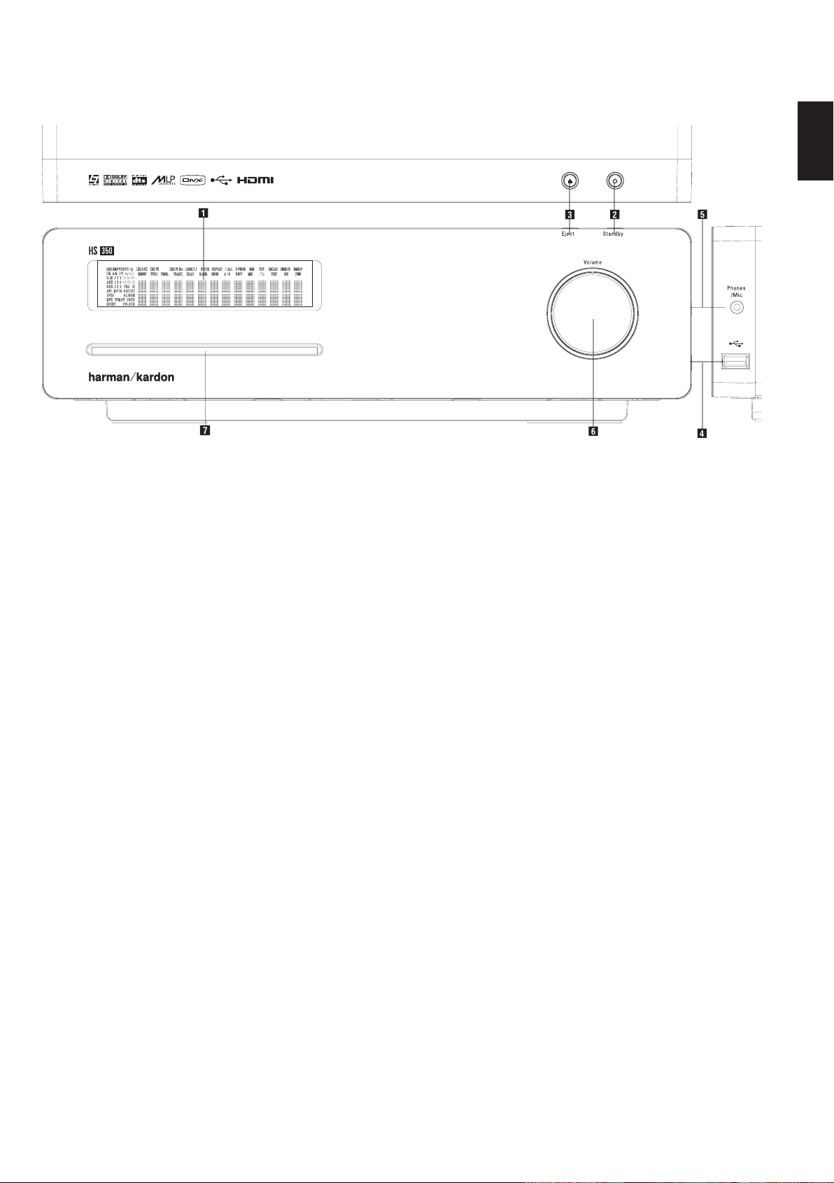
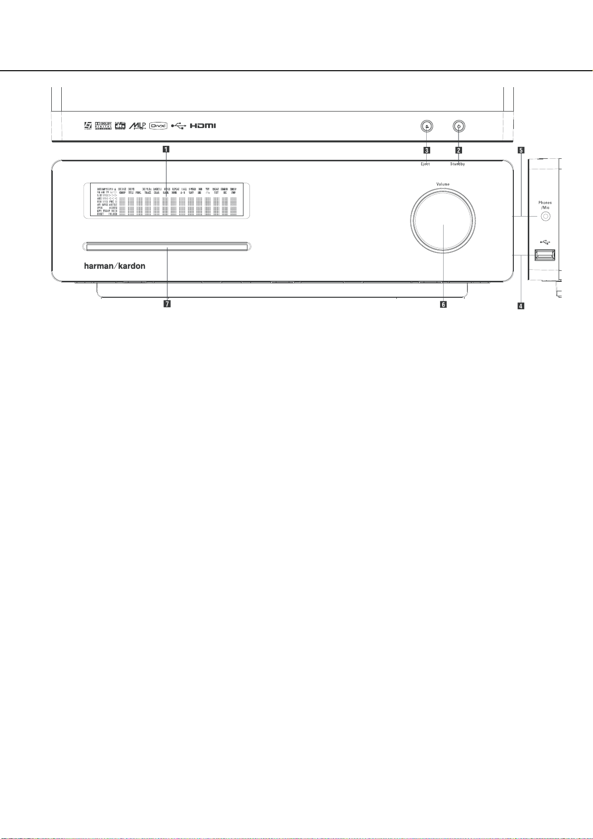
Front Panel Controls
harman/kardon
HS 350/650DL Service Manual
Page 5 of 89
HS 350
Main Information Display
1
Power On/Off (Standby)
2
Open/Close
3
USB On-The-Go Input
4
Headphone Jack
5
Volume Control
6
Slot Loader
ENGLISH
Main Information Display: This display
delivers messages and status indications to help
you operate the HS 350 Controller.
1
Power On/Off (Standby): Press the button
once to turn the HS 350Controller on, press it
again to put the unit in the Standby mode.
Note that when the HS 350 Controller is
switched on, the Power Indicator around the
button turns white.
2
Eject: Press this button to release a disc
from the loader.
3
USB On-The-Go Input: This input may be
used to temporarily connect a USB thumb device
or portable hard disk for direct playback of
audio, image of video files or a USB hub. The
USB inputs are designed to power a single USB
device at a time. If additional hard disks are
connected through a hub it is necessary that
additional external power supplies are used to
power the hub and hard disks.
4
Headphone Jack: This jack may be used to
listen to the system's output through a pair of
headphones. Be certain that the headphones
have a standard 3.5 mm stereo phone plug.
Note that the main room speakers will
automatically be turned off when the
headphone jack is in use.
When configuring your system using EzSet/EQ,
the calibration microphone should be plugged
into this jack
5
Volume Control:Turn this knob clockwise
to increase the volume, counterclockwise to
decrease the volume. If the system is muted,
adjusting volume control will automatically
release the unit from the silenced condition.
6
Slot loader: Gently insert a CD or DVD into
this slot, with the printed side of the disc facing
up. Note there is no drawer. Press the Eject
Button
4
.
2
to release the disc
Page 6
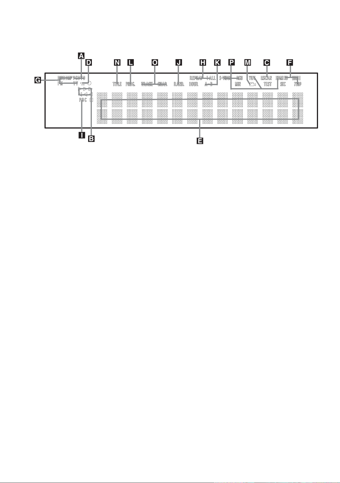
Front Panel Display
harman/kardon
HS 350/650DL Service Manual
Page 6 of 89
HS 350
A Disc Type Indicators
B Playback-Mode Indicators
C Progressive Scan Indicator
D Parental Lock Indicator
E Time Indicators
F Video Format Indicators
A Disc Type Indicators: The CD or DVD
indicator will illuminate to show the type of disc
currently being played.
B Playback-Mode Indicators: These
indicators light to show the current playback
mode:
N
Lights when a disc is playing in the normal
mode
H
Lights when the disc is in the Fast Search
Forward mode. The on-screen banner display
indicates the selected speed (2x, 8x, 16x, 100x).
1
Lights when the disc is paused.
G
Lights when the disc is in the Fast Search
Reverse mode. The on-screen banner display
indicates the selected speed (2x, 8x, 16x, 100x).
C Progressive Scan Indicator: This indicator
lights when the unit sends out a progressive
scan signal.
D Parental Lock Indicator: This indicator
lights when the parental-lock system is engaged
in order to prevent anyone from changing the
rating level without a code.
G Source Indicators
H Repeat Indicators
I VCD Playback Control Indicator
J Random Indicator
K A-B Repeat Indicator
L Program Indicator
E Time Indicators:These positions in the
indicator will show the running time of a DVD in
play. When a CD is playing, these indicators will
show the current track time, time remaining in
the current track, or the total remaining time on
the disc. When an iPod is playing, the display
will show the elapsed and remaining time on the
top line. The bottom line will scroll information
about the song, title, album and artist.
NOTE: The Indicators NOE will also display
text messages about the DVD’s status, including
Reading when a disc is loading,
STANDBY when the unit is turned off, and
Disc Error when a disc not compatible
with the DVD is put into the play position.
F Video Format Indicators:These indicators
will represent the video format currently playing.
G Source Indicators: These indicators will
light to show which source is currently selected.
H Repeat Indicators: These indicators light
when any of the Repeat functions are in use.
M Angle Indicator
N Title Indicators
O Chapter/Track Number Indicators
P Video Output Indicators
I VCD Playback Control Indicator:This
indicator lights when the playback control
function is turned on with VCDs.
J Random Indicator: This indicator lights
when the unit is in the Random Play mode.
K A-B Repeat Indicator: This indicator lights
when a specific passage for repeat playback has
been selected.
L Program Indicator: This indicator lights
when the programming functions are in use.
M Angle Indicator: This indicator blinks when
alternative viewing angles are available on the
DVD currently playing.
N Title Indicators: These two positions in the
display will show the current title number when
a DVD disc is playing.
O Chapter/Track Number Indicators: When
a DVD disc is playing, these two positions in the
display will show the current chapter. When a
CD disc is playing they will show the current
track number.
P Video Output Indicators: These indicators
will represent the active video output. .
Page 7
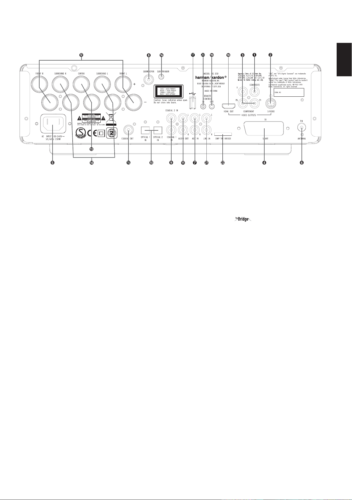
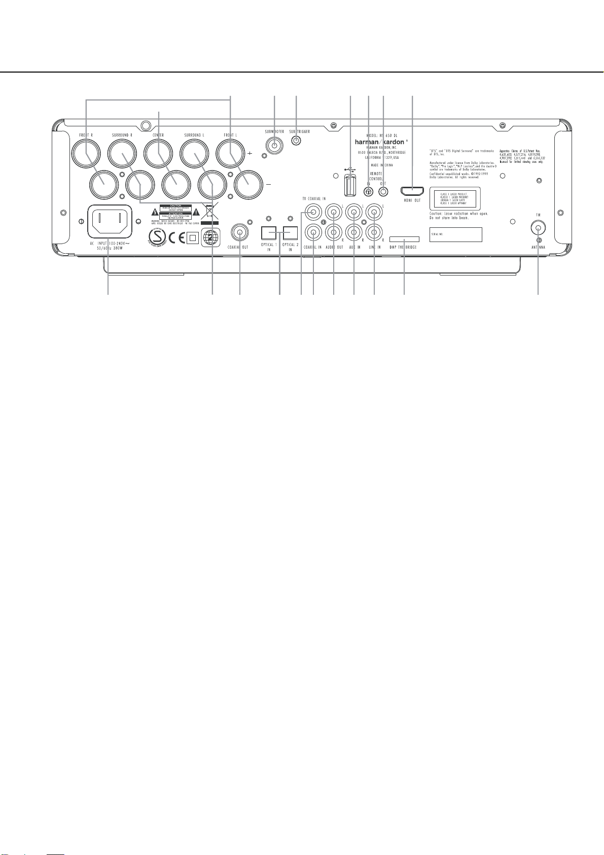
Rear Panel Connections
harman/kardon
HS 350/650DL Service Manual
Page 7 of 89
HS 350
0
Composite Video Output
1
S-Video Output
2
Component Video Outputs
3
Scart TV Output
4
AC Power Cord
5
FM Antenna
6
Audio In
7
Subwoofer Output
8
Coaxial Digital Input
9
Optical Digital Input
A
Analog Audio Outputs
B
Front Speaker Outputs
C
Center Speaker Outputs
D
Surround Speaker Outputs
E
Coaxial Digital Output
F
Subwoofer Trigger Output
G
USB On-The-Go Input
H
HDMI Output
I
Remote IR Output
J
Remote IR Input
K
TV Audio In
L
DMP Connector
ENGLISH
0
Composite Video Output: Connect this
jack to the video input on a television or video
projector.
1
S-Video Output: Connect this jack to the
S-Video input on a television or video projector.
2
Component Video Outputs: These outputs
carry the component video signals for connection
to display monitors with component video inputs.
For standard analog TV's or projectors with
inputs marked Y/Pr/Pb or Y/Cr/Cb, connect these
outputs to the corresponding inputs. If you have
a high-definition television or projector that is
compatible with high scan rate progressive video,
connect these jacks to the “HD Component”
inputs. Note that if you are using a progressive
scan display device, then ”Progressive” must be
selected in the Video Set-up Menu in order to
take advantage of the progressive scan circuitry.
See page 22 for more information on progressive
scan video.
IMPORTANT:These jacks should NOT be
connected to standard composite video inputs.
3
SCART OUT (TV): If your TV has a SCART
socket, you can connect a SCART cable to your
TV and to your DVD Player for improved video
quality. The SCART cable carries both audio and
video. You can select Composite Video or RGB
video for that SCART connector’s video output
signal.
4
AC Power Cord: Connect this plug to an AC
outlet. If the outlet is controlled by a switch,
make certain that it is in the ON position.
5
FM Antenna: Connect to the supplied FM
antenna.
6
Audio In: Connect to a line-level analog
audio source: TV, tape player, Minidisc, PC, etc.
7
Subwoofer Output: Connect to the
SUB/LFE input on the subwoofer.
8
Coaxial Digital Input: Connect the coax
digital output from a DVD player, HDTV receiver,
LD player, MD player, satellite receiver or CD
player to this jack. The signal may be either a
Dolby Digital signal, DTS signal or a standard
PCM digital source. Do not connect the RF digital
output of an LD player to these jacks.
9
Optical Digital Input: Connect the optical
digital output from a DVD player, HDTV receiver,
LD player, MD player, satellite receiver or CD
player to this jack. The signal may be either a
Dolby Digital signal, DTS signal or a standard
PCM digital source.
A
Analog Audio Outputs: Connect these
jacks to the analog audio input on a TV set or
external audio system for analog audio playback
or to the RECORD/INPUT jacks of an audio
recorder for recording.
B
Front Speaker Outputs: Connect these
outputs to the matching + or – terminals on your
left and right speakers. In conformance with the
new CEA color code specification, the White
terminal is the positive, or "+" terminal that
should be connected to the red (+) terminal on
Front Left speaker with the older color coding,
while the Red terminal is the positive, or "+"
terminal that should be connected to the red (+)
terminal on Front Right speaker. Connect the
black (–) terminals on the HS to the black (–)
terminals on the speakers. See page 14 for more
information on speaker polarity.
C
Center Speaker Outputs: Connect these
outputs to the matching + and – terminals on
your center channel speaker. In conformance with
the new CEA color code specification, the Green
Terminal is the positive, or "+" terminal that
should be connected to the red (+) terminal on
speakers with the older color coding. Connect
the black (–) terminal on the HS to the black
negative (–) terminal on your speaker. (See page
14 for more information on speaker polarity.)
Page 8

Rear Panel Connections
harman/kardon
HS 350/650DL Service Manual
Page 8 of 89
HS 350
D
Surround Speaker Outputs: Connect
these outputs to the matching + and – terminals
on your surround channel speakers. In conformance with the new CEA color code specification, the Blue terminal is the positive, or "+"
terminal that should be connected to the red (+)
terminal on the Surround Left speaker with older
color coding, while the Gray terminal should be
connected to the red (+) terminal on the
Surround Right speaker with the older color
coding. Connect the black (–) terminal on the HS
to the matching black negative (–) terminals for
each surround speaker. (See page 14 for more
information on speaker polarity.)
Note: You’ll find more details about all
Audio/Video connections under Setup and
Connections on the following pages.
E
Coaxial Digital Output: Connect this jack
to the matching digital input connector on a
digital recorder such as a CD-R or MiniDisc
recorder.
F
Subwoofer Trigger Output: Connect this
trigger output to the trigger input of the
Harman Kardon subwoofer, so that the
subwoofer will switch on and off at the same
time as the rest of the system.
G
USB On-The-Go Input: This input may be
used to temporarily connect a USB thumb device
or portable hard disk for direct playback of
audio, image of video files, a digital photo
camera or a USB hub.
H
HDMI Output: Connect this output to the
HDMI input of high-definition LCD, Plasma or
video projector for the best possible picture
quality.
I
Remote IR Output: This connection
permits the IR sensor in the receiver to serve
other remote controlled devices. Connect this
jack to the “IR IN” jack on Harman Kardon or
other compatible equipment.
J
Remote IR Input: If the HS 350’s frontpanel IR sensor is blocked due to cabinet doors
or other obstructions, an external IR sensor
may be used. Connect the output of the sensor
to this jack.
K
TV Audio Input: If your screen is
connected to the HS by an HDMI, Component,
S-Video or Composite cable, connect the
analog output of your TV to this input. If you
have your TV connected to the HS with a Scart
cable, an audio connection to the TV Input is
not necessary.
L
Digital Media Player (DMP)
Connector: With the HS 350 turned off,
connect one end of the optional Harman Kardon
to this proprietary connector, and the
other to your compatible Apple iPod. When the
Digital Media Player source is selected, you may
view your iPod’s control and navigation
messages on your video display (if one is
connected to one of the Video Monitor
Outputs
0123H
), and in the Upper
and Lower Display Lines E. You may
navigate the iPod and select tracks for playback
using the
⁄/¤/‹/›
Enter Button
Buttons9and the
6
.
Page 9
ENGLISH
Depth measurement includes knobs, buttons and terminal connections. Height measurement includes feet and chassis.
All features and specifications are subject to change without notice.
Harman Kardon The Bridge, and Logic 7 are registered trademarks of Harman International Industries, Incorporated.
Dolby, Pro Logic and the double-D symbol are trademarks of Dolby Laboratories, registered in the United States and/or other countries.
is a trademark of Harman International Industries, Inc.
All rights reserved.
DTS is a trademark of Digital Theater Systems, Inc.
Windows Media
®
Audio (WMA) is a proprietary file format developed by Microsoft.
DivX is a registered trademark of DivX, Inc.
HDMI, the HDMI logo and High-Definition Multimedia Interface are trademarks or registered trademarks of HDMI Licensing LLC.
Digital Lounge Controller Specifications
DVD player Pickup: Semiconductor laser, wavelength 650nm
Signal system: NTSC / PAL
Video signal horizontal resolution: More than 480 lines (DVD)
Video signal-to-noise ratio: More than 60 dB (DVD)
Audio frequency response: DVD (PCM): 20 Hz ~ 22 kHz (+/- 1.0 dB)
(Stereo) CD (PCM): 20 Hz ~ 20 kHz (+/- 1.0 dB)
Audio signal-to-noise ratio: More than 80 dB (PCM)
Total harmonic distortion:: Less than 0.01% (PCM)
Dynamic range: DVD (PCM): More than 85 dB (EIAJ, 2 kHz)
CD: More than 85 dB (EIAJ)
Amplifer output Power (per channel): 65 W (6ohms)
Signal-to-noise ratio: > 85 dB
Total Harmonic distortion: < 0.2%
FM Tuner System: PLL quartz-locked digital synthesizer system
Tuning range: 87.50 ~ 108.00 MHz
Antenna terminals: 75 ohms, unbalanced
Intermediate frequency: 10.7 MHz
Video Outputs: HDMI™ Output: Video: 576p, 720p, 1080i
HDMI Version 1.0-compliant
HDCP Version 1.1-compliant
Component Video Output: Y: 1 Vp-p/75 ohms, sync negative polarity
Cr: 0.7 Vp-p/75 ohms
Cb: 0.7 Vp-p/75 ohms
CVBS Video: 1 Vp-p 75 ohms
S-video: Y: 1 Vp-p 75 ohms
C: PAL 0.3 Vp-p 75 ohms / NTSC 0.286 Vp-p 75 ohms
Audio line Outputs Audio L/R: 2 Vrms, 1 kilohms
General Power requirements: AC 230 V, 50 Hz
Max power consumption: 500 W
Idle power consumption: Less than 2 W
Dimensions (WxHxD): 440 mm x 68 mm x 380 mm
Weight: 8.5 kg
* Designs and specifications are subject to change without notice.
harman/kardon
HS 350/650DL Service Manual
Page 9 of 89
DIGITAL LOUNGE 6XX
Page 10

ENGLISH
Troubleshooting
For the Controller
If you experience any of the following difficulties
while using the system, use this troubleshooting
guide to help you remedy the problem.
Should any problem persist, consult your authorized Harman Kardon dealer.
No power.
• Is the power cord firmly plugged into the
power outlet?
• One of the safety mechanisms may be operating. In this event, unplug the player from the
power outlet briefly and then plug it in again.
No picture.
• Check that the system is connected correctly
and securely.
• The video cable may be damaged. Replace it
with a new one.
• Make sure the system is connected to a video
input on the TV (see page 14).
• Make sure the TV is turned on.
• Make sure the correct video input on the TV is
selected for viewing with this system.
Noise (interference) appears in
the picture.
• Clean the disc.
• If video from this system has to go through
your VCR to get to your TV, the copy-protection
applied to some DVD programs could affect
picture quality. If you still experience pro blems
after checking your connecti ons, please try connecting your DVD system directly to your TV’s
S-Video input, if your TV is equipped with this
input (see page 14).
The aspect ratio of the screen is wrong
(picture vertically expanded) when you
play a wide picture by the player or an
external source connected to the screen
even though you set “TV DISPLAY” in the
SETUP menu to "Auto".
• If you connect the system or the external
source with the SCART cable, connect directly
to the TV. Otherwise the autoswitch function of
the aspect ratio for the TV may not work.
• If the TV is not connected with a SCART cable
to the HS (as recommended) or the external
source, or if the autoswitch function does not
work you should turn the TV to "Fill All".
There is no sound or volume is very low
• Check that the speakers and components are
connected correctly and securely.
• Make sure that you have selected the correct
source on the system.
• Press MUTE on the remote control, if the
words MUTE ON are blinking on the front
panel display.
• The protective circuitry has been activated
because of a short circuit. Turn off the system,
eliminate the short circuit problem and turn on
the power again.
• The audio interconnect is damaged. Replace it
with a new one.
• The system is in pause mode or in slow-motion
play mode, or fast forward or fast reverse.
Press
N
to return to normal play mode.
• Check the speaker settings (see page 19).
The left and right channels are
unbalanced or reversed.
• Check that the speakers and components are
connected correctly and securely.
Severe hum or noise is heard.
• Check that the speakers and components are
connected securely.
• Check that the connecting cords are away from
a transformer or motor and at least 3 meters
away from fluorescent light.
• Move your TV away from the audio components.
• The plugs and jacks are dirty. Wipe them with a
cloth slightly moistened with alcohol.
• Clean the disc.
• Disconnect antenna cables from external
sources (also PC) connected to the screen or
system. If hum disappears use an antenna
transfomer between antenna and source.
• If PC is connected to the system disconnect the
Audio and Video cables. If hum disappears use
an audio transformer between PC audio out
and system input. If hum persists unplug PC
from your system and ask your local dealer for
a proper solution (ground loop interrupt).
The surround effect is difficult to hear
when you are playing a Dolby Digital
sound track.
• Check to see if the Dolby Digital mode is
turned on properly, other wise unload and load
the disc again.
• Check the speaker connections.
• Depending on the DVD disc, the output signal
may at times be mono or stereo even if the
soundtrack is recorded in Dolby Digital format.
The sound comes from the
center speaker only.
• Depending on the disc, sound may sometimes
come from the center speaker only. This also
applies to mono recordings (from disc or any
analog source), when Pro Logic mode is selected. This is normal.
No sound is heard from the
center speaker.
• Adjust center speaker volume (see pages 19).
No sound or only very low volume
from the rear speakers.
• Adjust the rear speaker volume (see page 19).
The volume goes down automatically
and cannot be increased.
• The internal temperature is too high. Wait
approximately one minute for the amplifier to
reach normal working temperature.
Radio stations cannot be tuned in.
• Check that the antenna is connected correctly.
Adjust the antenna and connect an external
antenna if necessary.
• The signal strength of the stations is too weak
for automatic tuning. Use manual tuning.
• No stations have been preset.
• The tuner mode is not selected, select the
Radio mode.
The remote does not function.
• Remove any obstacles between the remote
control and the system.
• Move the remote control closer to the system.
• Point the remote control at the remote sensor
on the front panel.
• Replace all the batteries in the remote control
with new ones if they are weak.
• Check that the batteries are loaded correctly.
The disc does not play.
• There is no disc inside. (“NO DISC” appears on
the front panel display and the TV screen.)
Insert a disc.
• Insert the disc correctly with the playback side
facing down.
• Clean the disc.
• The system cannot play CD-ROM's, etc.
(see page 3).
• DVD with wrong region code
(see page 13).
Playback stops automatically.
• Some discs include an auto pause signal. When
playing such a disc, the system stops playback
at the signal.
harman/kardon
HS 350/650DL Service Manual
Page 10 of 89
DIGITAL LOUNGE 6XX
Page 11

Troubleshooting
Track Skip or direct select with numeric
buttons, Search, Slow-motion play, repeat
play or Program play, etc., cannot be
done.
• Depending on the DVD or VCD, some of the
above operations may not be available
(Playback control).
Messages do not appear on the TV screen
in the language you want.
• Select the language for Display and Preferred
Subtitle in the SETUP menu (see page 18).
For all messages from the DVD (DVD menu,
subtitles) in the proper language, the disc
must have the language you selected, if not,
another language will be selected.
The audio language cannot be changed
when you play a DVD.
• Multilingual sound is not recorded on the
DVD.
• Changing the language for the sound by the
Audio button on the remote or the Audio line
in the Player Menu is prohibited on the DVD.
In that case the audio language must be
selected by the main menu on the DVD.
The subtitle language cannot be changed
when you play a DVD.
• Multilingual subtitles are not recorded on the
DVD.
• Changing the language for the subtitles by the
Subtitle button on the remote or the Subtitle
line in the Player Menu is prohibited on the
DVD. In that case the subtitle language must
be selected by the main menu on the DVD.
The subtitles cannot be turned off when
you play a DVD.
• Depending on the DVD, you may not be able
to turn the subtitles off.
The angles cannot be changed when you
play a DVD.
• Multi-angles are not recorded on most DVDs.
• Change the angles when the angle mark
appears on the TV screen.
• Changing the angles is prohibited on some
DVDs.
The system does not operate properly.
• Static electricity, etc., may affect the system’s
operation.
Disconnect the AC power cord, then connect it
again.
Please also refer to the Trouble shooting
guide contained in your loudspeaker
Owners Manual
No picture although the mains plug is
inserted and the unit is switched on.
Screen dark.
Weak or excessive colours.
The picture is too large or too small.
The displayed picture is too dark.
The picture is displayed,
but there is no sound.
Horizontal stripes with TV
or video signals.
• Mains switch in position ”0” (OFF).
• Mains plug of unit is not inserted into
the plug receptacle.
• The HDMI cable is not properly inserted.
• Defective mains cable.
• Contrast setting too low.
• No input signal, wrong input selected.
• Colour not correctly set.
• Connection cable not correctly connected.
• Picture format set wrongly.
• The picture quality is not set correctly.
• The sound is switched to mute.
• The Coaxial Digital Audio cable is not properly
inserted.
• Volume is set to minimum.
• Signal source is placed in front of the display.
• Shift mains switch to position ”I”.
• Insert the mains cable plug into the
plug receptacle.
• Insert the HDMI cable firmly.
• Call the service hotline.
• Set the brightness and/or contrast correctly
(see Picture Calibration).
• Check the connection cable; assign correct
input to source.
• Set the colour correctly
(see Picture Calibration).
• Connect the cable correctly.
• Repeatedly press the Screen Format Button
until the picture is displayed as full
screen.
• Correct the picture brightness and contrast
(see Picture Calibration)
• Press the Mute Button
A
on the remote
control.
• Insert the Coaxial Digital Audio cable firmly.
• Increase the volume.
• Always place the signal sources on the side of
or behind the display.
Defect Possible cause Possible remedy
For the TV
harman/kardon
HS 350/650DL Service Manual
Page 11 of 89
DIGITAL LOUNGE 6XX
Page 12
Digital Louge
Front Panel Controls
Main Information Display
1
Power On/Off (Standby)
2
Open/Close
3
USB On-The-Go Input
4
Headphone Jack
5
Volume Control
6
Slot Loader
Main Information Display: This display
delivers messages and status indications to help
you operate the Digital Lounge Controller.
1
Power On/Off (Standby): Press the button
once to turn the Digital Lounge Controller on,
press it again to put the unit in the Standby
mode.
Note that when the Digital Lounge Controller is
switched on, the Power Indicator around the
button turns blue.
2
Eject: Press this button to release a disc
from the loader.
3
USB On-The-Go Input: This input may be
used to temporarily connect a USB thumb device
or portable hard disk for direct playback of
audio, image of video files or a USB hub. The
USB inputs are designed to power a single USB
device at a time. If additional hard disks are
connected through a hub it is necessary that
additional external power supplies are used to
power the hub and hard disks.
4
Headphone Jack: This jack may be used to
listen to the system's output through a pair of
headphones. Be certain that the headphones
have a standard 3.5 mm stereo phone plug.
Note that the main room speakers will
automatically be turned off when the
headphone jack is in use.
When configuring your system using EzSet/EQ,
the calibration microphone should be plugged
into this jack
4
.
5
Volume Control:Turn this knob clockwise
to increase the volume, counterclockwise to
decrease the volume. If the system is muted,
adjusting volume control will automatically
release the unit from the silenced condition.
6
Slot loader: Gently insert a CD or DVD into
this slot, with the printed side of the disc facing
up. Note there is no drawer. Press the Eject
Button
2
to release the disc
harman/kardon
HS 350/650DL Service Manual
Page 12 of 89
DIGITAL LOUNGE 6XX
Page 13
ENGLISH
Front Panel Display
A Disc Type Indicators
B Playback-Mode Indicators
C Progressive Scan Indicator
D Parental Lock Indicator
E Time Indicators
F Video Format Indicators
G Source Indicators
H Repeat Indicators
I VCD Playback Control Indicator
J Random Indicator
K A-B Repeat Indicator
L Program Indicator
M Angle Indicator
N Title Indicators
O Chapter/Track Number Indicators
P Video Output Indicators
A Disc Type Indicators: The CD or DVD
indicator will illuminate to show the type of disc
currently being played.
B Playback-Mode Indicators: These
indicators light to show the current playback
mode:
N
Lights when a disc is playing in the normal
mode
H
Lights when the disc is in the Fast Search
Forward mode. The on-screen banner display
indicates the selected speed (2x, 8x, 16x, 100x).
1
Lights when the disc is paused.
G
Lights when the disc is in the Fast Search
Reverse mode. The on-screen banner display
indicates the selected speed (2x, 8x, 16x, 100x).
C Progressive Scan Indicator: This indicator
lights when the unit sends out a progressive
scan signal.
D Parental Lock Indicator: This indicator
lights when the parental-lock system is engaged
in order to prevent anyone from changing the
rating level without a code.
E Time Indicators:These positions in the
indicator will show the running time of a DVD in
play. When a CD is playing, these indicators will
show the current track time, time remaining in
the current track, or the total remaining time on
the disc. When an iPod is playing, the display
will show the elapsed and remaining time on the
top line. The bottom line will scroll information
about the song, title, album and artist.
NOTE: The Indicators NOE will also display
text messages about the DVD’s status, including
Reading when a disc is loading,
STANDBY when the unit is turned off, and
Disc Error when a disc not compatible
with the DVD is put into the play position.
F Video Format Indicators:These indicators
will represent the video format currently playing.
G Source Indicators: These indicators will
light to show which source is currently selected.
H Repeat Indicators: These indicators light
when any of the Repeat functions are in use.
I VCD Playback Control Indicator:This
indicator lights when the playback control
function is turned on with VCDs.
J Random Indicator: This indicator lights
when the unit is in the Random Play mode.
K A-B Repeat Indicator: This indicator lights
when a specific passage for repeat playback has
been selected.
L Program Indicator: This indicator lights
when the programming functions are in use.
M Angle Indicator: This indicator blinks when
alternative viewing angles are available on the
DVD currently playing.
N Title Indicators: These two positions in the
display will show the current title number when
a DVD disc is playing.
O Chapter/Track Number Indicators: When
a DVD disc is playing, these two positions in the
display will show the current chapter. When a
CD disc is playing they will show the current
track number.
P Video Output Indicators: These indicators
will represent the active video output. .
harman/kardon
HS 350/650DL Service Manual
Page 13 of 89
DIGITAL LOUNGE 6XX
Page 14
Rear Panel Connections
D
HDMI Output
Remote IR Output
Remote IR Input
USB On-The-Go Input
AC Power Cord
FM Antenna
Audio In
Subwoofer Output
Coaxial Digital TV Input
Optical Digital Input
Analog Audio Outputs
Front Speaker Outputs
Center Speaker Outputs
Surround Speaker Outputs
Coaxial Digital Output
Subwoofer Trigger Output
Coaxial Digital Input
DMP The Bridge Input
Analog Audio Inputs
HDMI Output: Connect this output to the
HDMI input
J
of the screen, using the supplied
HDMI - SP-DIF - Remote In/Out cable.
Remote IR Output: This connection permits the IR sensor in the receiver to serve other
remote controlled devices. Connect this jack to
the “IR IN” jack on Harman Kardon or other
compatible equipment. Note this connection is
only necessary for optional, additional products
connected to the player. It is not necessary for
proper control of the Digital Lounge system.
Remote IR Input: Connect this input to the
Remote IR Output
U
of the TV, using the special
HDMI - SP-DIF - Remote In/Out cable. This will
allow you to control all components in your system by pointing the remote control to the TV
only.
USB On-The-Go Input: This input may be
used to temporarily connect a USB thumb device
or portable hard disk for direct playback of
audio, image of video files, a digital photo camera or a USB hub.
AC Power Cord: Connect this plug to an
AC outlet. If the outlet is controlled by a switch,
make certain that it is in the ON position.
FM Antenna: Connect to the supplied FM
antenna.
Audio In: Connect to a line-level analog
audio source: TV, tape player, Minidisc, PC, etc.
Subwoofer Output: Connect to the
SUB/LFE input on the subwoofer.
Coaxial Digital TV Input: Connect the
Coax Digital TV Output
H
of the screen to this
jack, using the supplied HDMI - SP-DIF - Remote
In/Out cable.
Optical Digital Input: Connect the optical
digital output from a DVD player, HDTV receiver,
LD player, MD player, satellite receiver or CD
player to this jack. The signal may be either a
Dolby Digital signal, DTS signal or a standard
PCM digital source.
Analog Audio Outputs: Connect these
jacks to the RECORD/INPUT jacks of an optional
audio recorder for recording.
Front Speaker Outputs: Connect these
outputs to the matching + or – terminals on
your left and right speakers. In conformance with
the new CEA color code specification, the White
terminal is the positive, or "+" terminal that
should be connected to the red (+) terminal on
Front Left speaker with the older color coding,
while the Red terminal is the positive, or "+"
terminal that should be connected to the red (+)
terminal on Front Right speaker. Connect the
black (–) terminals on the Digital Lounge system
to the black (–) terminals on the speakers. See
page 15 for more information on speaker polarity.
Center Speaker Outputs: Connect these
outputs to the matching + and – terminals on
your center channel speaker. In conformance
with the new CEA color code specification, the
Green Terminal is the positive, or "+" terminal
that should be connected to the red (+) terminal on speakers with the older color coding.
Connect the black (–) terminal on the Digital
Lounge system to the black negative (–) terminal
on your speaker. (See page 15 for more information on speaker polarity.)
harman/kardon
HS 350/650DL Service Manual
Page 14 of 89
DIGITAL LOUNGE 6XX
C
0
123F7B
4 E
9 8G A 6 I H 5
Page 15
16
harman/kardon
HS 350/650DL Service Manual
Page 15 of 89
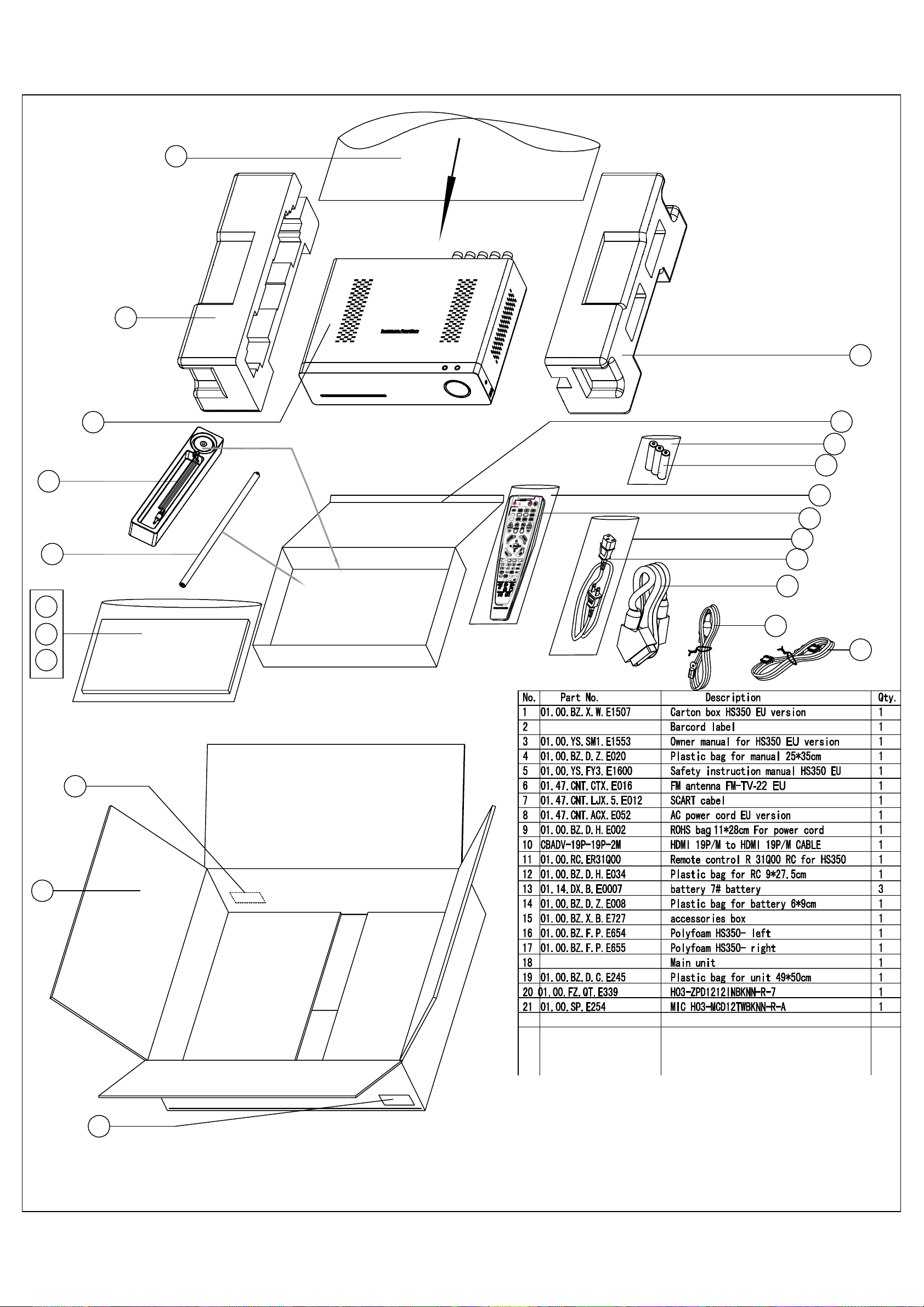
HS 350 PACKAGE LIST AND PARTS
19
17
21
20
5
4
3
18
15
14
13
12
11
9
8
7
6
10
2
1
2
HS350 EU Packing instruction
Drawing by. : Jenniferzph
May,10'2008
Page 16
13
harman/kardon
HS 350/650DL Service Manual
Page 16 of 89
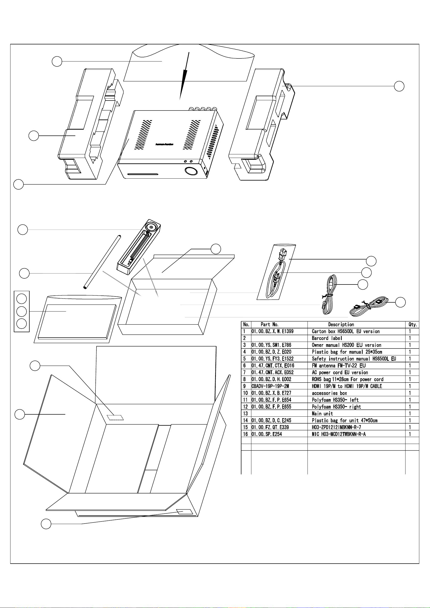
HS 650 PACKAGE LIST AND PARTS
14
12
11
16
15
5
4
3
10
8
7
6
9
2
1
2
HS650DL EU Packing instruction
Drawing by. : Jenniferzph
May,10'2008
Page 17
harman/kardon
HS 350/650DL Service Manual
Page 17 of 89
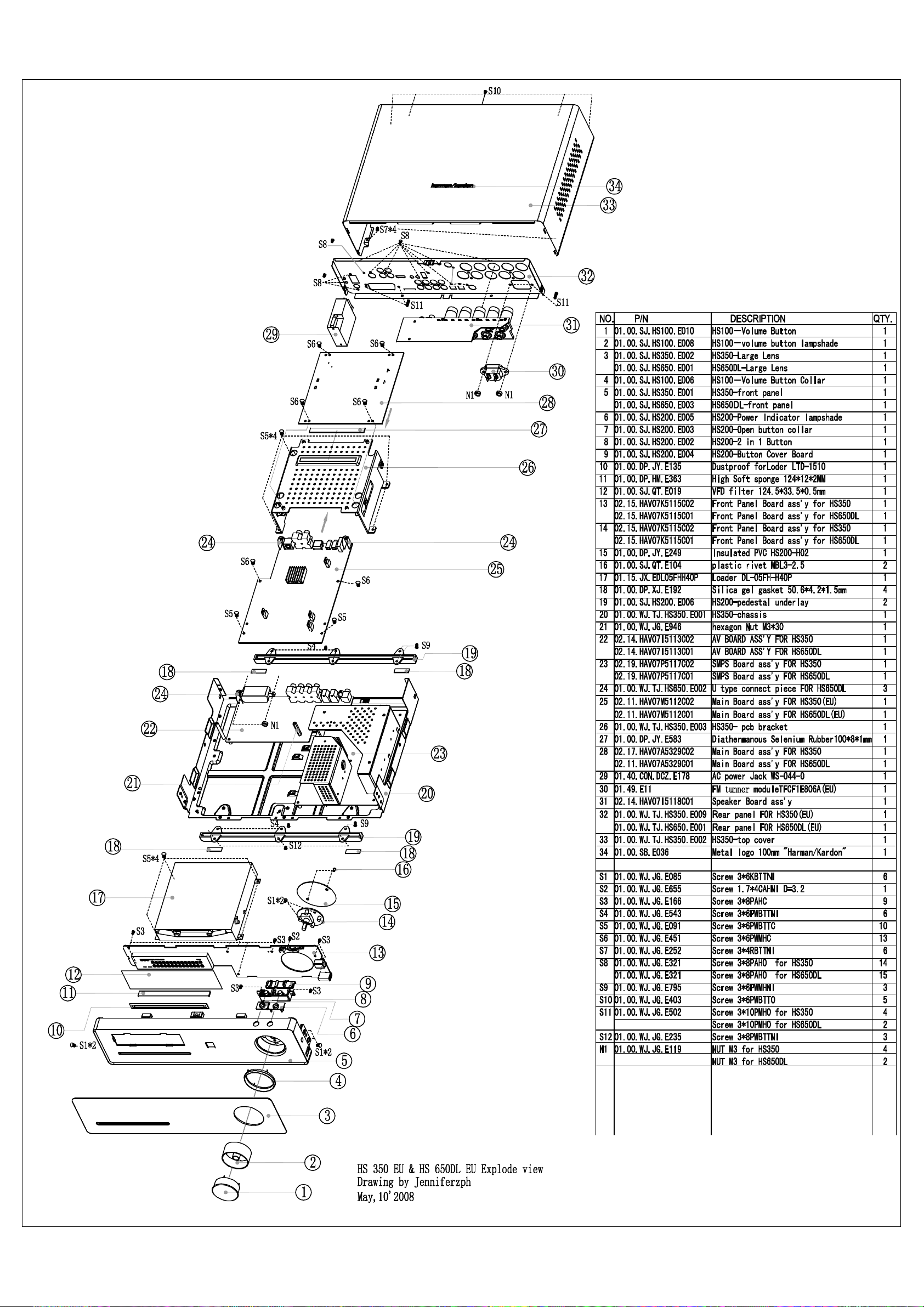
HS 350/230 and HS/DL 650/230 EXPLODED VIEW
Page 18
HS650DL Component List
t
t
r
t
p
t
t
d
k
d
k
d
k
d
k
d
k
t
3
t
2
t
r
3
t
6
t
4
p
t
y
6
t
s
t
0
p
g
0
r
m
k
g
r
g
)
g
)
g
)
p
g
)
t
r
2
r
d
9
g
)
4
g
)
(2)
y(6)
y(3)
p
)
y(9)
(4)
)
(4)
harman/kardon
HS 350/650DL Service Manual
Page 18 of 89
Location.No. Description Specification P/N
HS350-PT01 Metals Par
HS350-PT02 Metals Par
HS650DL-PT01 Metals Par
HS650DL-PT02 Metals Part
HS350-PT04 Metals Par
For S702 on SMPS boar
For S703 on SMPS boar
For S704 on SMPS boar
For S704 and S703 on SMPS boar
For S701 on SMPS board Heatsink
HS350-PT10 Between AV board and
Mainboard
For U4 on Mainboar
HS350-RE01 plastic par
HS200-RE02 plastic par
HS200-RE03 plastic par
HS100-RE06 plastic par
HS200-RE04 plastic par
HS200-RE05 plastic part
HS200-RE06 plastic par
HS350-RE02 plastic par
HS100-RE10 plastic par
HS100-RE08 plastic part
Add on Power cord Ma
Black color
For pedestal underlay HS100-H01 Silica gel gasket
For VFD (2) sponge
Between volume button and Front Panel
Board
Inside the volume button Mask PVC
For IR receiver sponge
paste in front of Disc tray door in the front
anel
Between Front Panel Board and Plastic Par
For Q509 on SMPS board Sil-pad sil-pad 400-302
For Amplifier board
Be buckled above volume button boar
For hamulus of front panel Insulated PVC
Between Tuner and chassis sponge
For Front Panel and Left/Right sides of
chassis (4),For Front Panel and Volume
Board
For chassis and pedestal underla
For chassis and pedestal underla
For Front panel board and chassis and
edestal underlay(3
For Front panel and Front panel board/ke
For Loader and chassis(4),For PCB Bracket
and chassis
For SMPS board and chassis(6),For AV board
and chassis(1),For Mainboard(2),For Amplifier
board and Bracket
,For Mainboar and Bracket(2
Heatsin
Heatsin
Heatsin
Heatsin
Hexagonal Nut M3*30 01.00.WJ.JG.E946
Heatsin
plastic part
netism annulusM248 01.13.L.H.E02
VFD filte
AC power Jac
Metal logo
Dustproof for Disc tray
door of Lode
Astigmatism PVC Φ45.5*Φ9.5mm 01.00.FZ.QT.153
High Soft sponge
electric sponge 20*20*10MM 01.00.DD.PM.E271
Plastic fastene
Diathermanous
Selenium Rubbe
Insulated PVC HS200-H02 01.00.DP.JY.E24
Insulated PVC HS350-H01 01.00.DP.JY.E13
Screw 3*6KBTTNI 01.00.WJ.JG.E085
Screw 3*6PWBTTNI 01.00.WJ.JG.E543
Screw 3*6PWMHNI 01.00.WJ.JG.E795
Screw 3*8PWBTTNI 01.00.WJ.JG.E235
Screw 3*8PAHC 01.00.WJ.JG.E166
Screw 3*6PWBTTC W=7 01.00.WJ.JG.E091
Screw 3*6PWMHC W=7 01.00.WJ.JG.E451
HS350-chassis 01.00.WJ.TJ.HS350.E001
HS350-top cove
HS650DL-rear panel 01.00.WJ.TJ.HS650.E001
HS650DL-U type connect
iece
HS350-PCB bracke
HS350-PT05100*55*55 01.00.WJ.TJ.HS350.E004
HS350-PT0667*53*22 01.00.WJ.TJ.HS350.E005
HS350-PT07143*53*22 01.00.WJ.TJ.HS350.E006
HS350-PT08143*134*2 01.00.WJ.TJ.HS350.E007
HS350-PT0935*11*48(Hole
height is 18mm)
28*28*10mm 01.00.WJ.TJ.E268
HS650-front pannel 01.00.SJ.HS650.E00
HS200-2 in 1 Button 01.00.SJ.HS200.E00
HS200-Open button colla
HS100-Volume Button Collar01.00.SJ.HS100.E00
HS200-Button Cover Board 01.00.SJ.HS200.E00
HS200-Power Indicator
lam
shade
HS200-pedestal underla
HS650DL-Large Len
HS100-Volume Button 01.00.SJ.HS100.E01
HS100-Volume Button
Lam
shade
1000A-IR receiver support
5.5mm
124.5*33.5*0.5m
WS-044-0 01.40.CON.DCZ.E178
100mm "Harman/Kardon" Thin
o
Lo
LTD-1510 01.00.DP.JY.E135
50.6*4.2*1.5mm (with #500
lue be single sides glued
20*10*5MM (with #9448 glue
be double sides
φ38.5(Underside Glued)Black
color, PVC
10*10*7MM (with double sides
lued
124*10*2MM (with Single side
lued,Black color
12CM 01.00.FZ.QT.E122
100*8*1mm 01.00.DP.JY.E583
22.5*10*0.3mm(with Single
side
lued
20*10*8MM(with double sides
lued
lued
01.00.WJ.TJ.HS350.E002
01.00.WJ.TJ.HS650.E002
01.00.WJ.TJ.HS350.E003
01.00.WJ.TJ.HS350.E008
01.00.SJ.HS200.E00
01.00.SJ.HS200.E005
01.00.SJ.HS200.E00
01.00.SJ.HS650.E001
01.00.SJ.HS100.E008
01.00.SJ.1000A.E016
01.00.SJ.QT.E019
01.00.SB.E036
01.00.DP.XJ.E192
01.00.DP.HM.E117
01.00.FZ.QT.E253
01.00.DP.HM.E364
01.00.DP.HM.E378
01.00.DP.QT.E113
01.00.DP.JY.E541
01.00.DP.HM.E263
Page 19
HS650DL Component List
(4)
p
)
p
)
(2)
(10)
g
(1)
j
)
(2M)
)
r
)
e
(
)
(
)
p
)
p
)
p
p
d
A
6
d
A
8
A
5
g
)
)
g
)
g
)
g
)
g
)
g
)
g
)
harman/kardon
HS 350/650DL Service Manual
Page 19 of 89
Location.No. Description Specification P/N
For Rear panel and chassis(2),For Top cover
and the bottom side of chassis
For output jacks(10),For frequency modulation
module(2),For U type connect piece and rear
anel(3
For top cover and chassis, top cover and rear
anel(5
For AC power socket
For IC and Heatsinks on SMPS board
Heatsinks on SMPS board3 Screw 3*6PWMTTC W=7 01.00.WJ.JG.E093
Amon
For Button cover Board and button Board Screw 1.7*4CAHNI D=3.2 Free-Lead 01.00.WJ.JG.E655
BD701 fixed with Heatsink on SMPS board
For power
For uncovered Screw drilled through the
chassis
For Insulated gasket and volume button Board Plastic Rivet MBL3-2.5 01.00.SJ.QT.E104
WS-002E+WS-019 HO5VV-F 0.75×2C BK 2M Power Cord
IEC Head for FM Connector (NON-Screw
Thread
CN701 on SMPS to Power Jack with solder
one end
CN706 on SMPS to CN403 on Amplifier board Connect cable
CN405 on Amplifier board to CN902 on
eaker board
S
Connect ground beside headphone jack to
SMPS
CN601(A) on Front panel board to CN5(A) on
Mainboard
CN6(C) on Mainboard to CN704(C) on SMPS
board
CN9(D) on Mainboard to CN301(D) on AV
board,CN8(E) on Mainboard to CN302(E) on
AV board
CN7(F) on Mainboard to CN303(F) on AV
board
CN702(G) on SMPS board to CN602(G) on
Front
CN703(I) on SMPS board to CN402(I) on
Am
CN404 on Amplifier to CN901 on Speaker
board
CN4(B) on Mainboard to CN401 on Amplifier
board
CN604(J) on Front panel board to CN605(J)
on Volume board
Loader to CN2 on Mainboar
Loader to CN1 on Mainboar
Tuner to CN304 on AV board Flat cable 1.25*11P*70mm
4-layers
2-layers
2-layers
2-layers
2-layers
4-layers
2-layers
ack(2
anel board
lifier board
Screw 3*4RBTTNI 01.00.WJ.JG.E252
Screw 3*8PAHO 01.00.WJ.JG.E321
Screw 3*6PWBTTO 01.00.WJ.JG.E403
Screw 3*10 PMHO 01.00.WJ.JG.E502
Screw 3*6PBTTC 01.00.WJ.JG.E087
Screw 3*8PBTTC 01.00.WJ.JG.E417
Nut M3 01.00.WJ.JG.E119
Screw Jacket Ф3*4mm 01.00.FZ.TG.E025
HDMI Cord 1770261-1
Microphone H03-MCD12TWBKNN-R-A 01.00.SP.E254
Antenna
Loade
FM frequency
modulation modul
Connect cable
Connect cable
Connect cable
Flat cable 1.0*22P*80mmA 01.48.BPX.1.E170
Flat cable 1.25*16P*80mmA(T=0.1mm) 01.48.BPX.1.E171
Flat cable 1.0*20P*70mmA 01.48.BPX.1.E172
Flat cable 1.25*18P*70mmA(T=0.1mm) 01.48.BPX.1.E173
Flat cable 1.25*14P*110mmA(T=0.1mm) 01.48.BPX.1.E174
Flat cable 1.25*6P*110mmA(T=0.1mm) 01.48.BPX.1.E176
Flat cable 1.0*8P*50mmA 01.48.BPX.1.E177
Flat cable 1.0*16P*80mmA 01.48.BPX.1.E150
Flat cable 1.0*6P*40mmA 01.48.BPX.1.E154
Flat cable 1.0*12P*220mm
Flat cable 0.5*24P*200mm
Main Board (semimanufactured
AV Board (semimanufactured
Speaker Board (semimanufactured
Front panel Board
(semi-manufactured
oods
Front panel Board
(semi-manufactured
oods
Amplifier Board (semimanufactured
SMPS Board (semimanufactured
WS-002E+WS-019 HO5VV-F
0.75×2C BK 2M
FM-TV-22 (Lead content less
than 300PPM
DL-05MH-H40P 01.15.JX.EDL05MH
TFCF1E806A 01.49.E11
VH-3Y Connector-2Y-
240mm
VH-4Y Connector-4Y-4Y150mm
VH-10Y Connector-10Y-10Y100mm(Be different side
70mm single-core cable (with
solder one end and ground
HAV07M-5112C01(EU
oods
Version+Hitachi Loader
HAV07I-5113C01(EU Version) 02.14.HAV07I5113C01
oods
HAV07I-5118C01 02.14.HAV07I5118C01
oods
HAV07K-5115C01 02.15.HAV07K5115C01
HAV07K-5116C01 02.15.HAV07K5116C01
HAV07A-5329C01 02.17.HAV07A5329C01
oods
HAV07P-5117C01 02.19.HAV07P5117C01
oods
Be same side
Be same side
iece φ4 connect another end
01.47.CNT.LJX.5.E241
01.47.CNT.ACX.E052
01.47.CNT.CTX.E016
01.47.CNT.LJX.7.E776
01.47.CNT.LJX.7.E726
01.47.CNT.LJX.7.E777
01.47.CNT.LJX.7.E795
01.48.BPX.1.E15
01.48.BPX.1.E02
01.48.BPX.1.E08
02.11.HAV07M5112C01
Page 20
HS650DL Component List for Main Board (5112C01)
(
(
)
F
K
K
K
2
K
K
(
)
K
K
K
2
(
)
F
K
K
K
K
K
5
p
k
p
k
p
k
p
k
p
p
p
p
p
p
p
p
harman/kardon
HS 350/650DL Service Manual
Page 20 of 89
Location.No. Description Specification P/N
R4 R9 R45 R49 R50 R174 R202 R205 R207
R215 (R219) R223 R224 R225 R227 R228
R229 R230 R231 R233 R238 R239 FB17
FB19
R156 R158 Resistor, chip 0603-10Ω±5% 01.57.R.2.E100J
R42 R43 R61 R62 Resistor, chip 0603-20Ω±5% 01.57.R.2.E200J
R29 R30 (R31) R32 (R33) R34 (R35) R36
R37) R38
R2 R47 R124 R125 R126 R127 R142 R145
R146 R147 R149 R150 R151 R153 R155
R211
R201
R6 (R41) (R71) (R120) (R121) R130 R177
R221
R206 Resistor, chip 0603-150Ω±5% 01.57.R.2.E151J
R8 R235 Resistor, chip 0603-200Ω±5% 01.57.R.2.E201J
R19 Resistor, chip 0603-220Ω±5% 01.57.R.2.E221J
R173 Resistor, chip 0603-270Ω±5% 01.57.R.2.E271J
R167 Resistor, chip 0603-390Ω±5% 01.57.R.2.E391J
R141 Resistor, chip 0603-475Ω±1% 01.57.R.2.E4750
R26 R77 R58 Resistor, chip 0603-1KΩ±5% 01.57.R.2.E102J
R80 R83 Resistor, chip 0603-1.2
R79 R86 Resistor, chip 0603-1.5
R69 R160 R161 Resistor, chip 0603-1.8
R13 R14 R15 R16 R18 R87 R9
R204 Resistor, chip 0603-2.2
R65 Resistor, chip 0603-3
R11) R88 R209 R210 (R232
R44 R46 R52 Resistor, chip 0603-3.9
R5 R10 R21 R27 R55 R57 R63 R67 R96
R162 R163 R168 R170 R178 R185 R186
R190 R191 R192
R89 Resistor, chip 0603-5.1
R91 Resistor, chip 0603-6.8
R12 R20 R24 R25 R28 R56 R64 R66 R68
R75 R76 R78 R81 R82 R122 R123 R128
R129 R143 R144 R171 R17
R48
R72
R17 Resistor, chip 0603-15KΩ±5% 01.57.R.2.E153J
R84 R85 Resistor, chip 0603-22
R40 Resistor, chip 0603-24
R90 Resistor, chip 0603-27
R53 Resistor, chip 0603-33
R51 Resistor, chip 0603-39
R22 R54 R93 R95 R16
R73 Resistor, chip 0603-1MΩ±5% 01.57.R.2.E105J
R59 R60 Resistor, chip 0805-2Ω±1% 01.57.R.3.E2R0F
R3 Resistor, chip 1206-2Ω±5% 01.57.R.4.E020J
RN4
RN6 RN7 RN8 RN9 RN10 RN11
RN3
RN1
PTC1
C192
(C65) (C64) (C147) (C146)
C97 C112
C103 C116
C84 C87 C115
C129
C82 C86 C90
C105 C106 C108 C111
Resistor, chip 0603-0Ω ±5% 01.57.R.2.E000J
Resistor, chip 0603-22Ω±5% 01.57.R.2.E220J
Resistor, chip 0603-33Ω±5% 01.57.R.2.E330J
Resistor, chip 0603-100Ω±5% 01.57.R.2.E101J
Ω±5% 01.57.R.2.E122J
Ω±5% 01.57.R.2.E152J
Resistor, chip 0603-2KΩ±5% 01.57.R.2.E202J
Resistor, chip 0603-3.3KΩ±5% 01.57.R.2.E332J
Resistor, chip 0603-4.7KΩ±5% 01.57.R.2.E472J
Resistor, chip 0603-10KΩ±5% 01.57.R.2.E103J
Resistor, chip 0603-12KΩ±1% 01.57.R.2.E123
Resistor, chip 0603-47KΩ±5% 01.57.R.2.E473J
Resistor, thick film
networ
chi
Resistor, thick film
chi
networ
Resistor, thick film
chi
networ
Resistor, thick film
chi
networ
Thermmal Dependent
Resistor, JinKe
Capacitor, multilayer
ceramic, chi
Capacitor, multilayer
ceramic, chi
Capacitor, multilayer
ceramic, chi
Capacitor, multilayer
ceramic, chi
Capacitor, multilayer
ceramic, chi
Capacitor, multilayer
ceramic, chi
Capacitor, multilayer
ceramic, chi
Capacitor, multilayer
ceramic, chi
0603-10Ω*4 ±5% 01.57.R.8.EP1004
0603-33Ω*4 ±5% 01.57.R.8.EP3304
0603-4.7KΩ*4 ±5% 01.57.R.8.EP4724
0603-10KΩ*4 ±5% 01.57.R.8.EP1034
JK-MSMD050 SMD 01.57.R.R.E050
0603-3.3P NPO±0.25%/50V 01.54.CS.2.E3P3N50V
0603-6.8P NPO±0.25PF/50V 01.54.CS.2.E6P8N50V
0603-100P NPO±5%/50V 01.54.CS.2.E101N50V
0603-180P NPO±5%/50V 01.54.CS.2.E181N50V
0603-220P NPO±5%/50V 01.54.CS.2.E221N50V
0603-390P NPO±5%/50V 01.54.CS.2.E391N50V
0603-470P X7R±10%/50V 01.54.CS.2.E471X50V
0603-680P X7R±10%/50V 01.54.CS.2.E681X50V
Ω±5% 01.57.R.2.E182J
Ω±5% 01.57.R.2.E222J
Ω±5% 01.57.R.2.E302J
Ω±5% 01.57.R.2.E392J
Ω±5% 01.57.R.2.E512J
Ω±5% 01.57.R.2.E682J
Ω±5% 01.57.R.2.E223J
Ω±5% 01.57.R.2.E243J
Ω±5% 01.57.R.2.E273J
Ω±5% 01.57.R.2.E333J
Ω±5% 01.57.R.2.E393J
Page 21
HS650DL Component List for Main Board (5112C01)
p
p
p
p
p
p
p
p
p
p
(
)
p
(
)
p
ytic
ytic
2
ytic
ytic
ytic
ytic
(
0
harman/kardon
HS 350/650DL Service Manual
Page 21 of 89
Location.No. Description Specification P/N
C91 C94 C96 C99 C118 C119
(C19)
(C20)
C113 C114 C120
C191
C88
C6 C8
C101
C16 C117 C127 C136
(C107) C121
C1 C2 C3 C4 C5 C7 C9 C10 (C11) C12 C13
(C14) (C15) (C17) C18 (C21) (C22) C23 (C24)
C25 (C26) (C27) (C28) (C29) (C30) C31 (C32)
(C33) (C34) (C35) (C36) (C37) (C38) (C39)
C40 C41 C42 (C43) (C44) (C45) (C46) (C47)
(C48) (C49) (C50) (C51) (C52) (C53) (C54)
(C55) (C56) (C57) (C58) (C59) (C60) (C61)
C62 (C63) C66 (C67) (C68) (C69) (C70) (C71)
(C72) (C73) (C74) (C75) (C76) (C77) C78
(C79) (C80) C81 C83 C85 C89 C92 (C93)
(C95) C98 C102 C104 C109 (C110) C122
C123 C124 (C125) C126 (C128) C130 C131
C132 (C133) (C134) (C135) C148 (C149)
(C150) C151 (C152) (C153) (C154) (C155)
(C156) (C157) (C158) (C159) C163 (C164)
C165
C100 (C194) (C195) (C196) (C197) (C198)
C199) C204 (C206) (C0
C166 C168 C169 (C170) (C171) (C172)
(C173) (C174) (C175) (C176) (C177) C178
C179 (C180) (C181) C182 C183 C184 C185
C186 (C187) C188 C189 (C202) C203 (C207)
(C208) (C209) (C210) (C211) (C212) (C213)
(C214) C215 (C216) (C217) (C218) (C219)
(C220) C221 (C222) (C223) (C224) C225
C226 (C227) C228 C229 (C230) (C231)
(C232) (C233) (C234) (C235) (C236) (C237)
(C238) (C239) (C240) (C241) (C242) (C243)
C244) (C245) (C246) (C247) (C248
C193
CE4 CE46 CE47
CE43 CE44 CE45
CE1 CE3 CE5 CE6 CE7 CE8 CE9 CE10
CE11 CE16 CE17 CE18 CE19 CE22 CE23
CE50 CE52 CE54 CE201 CE20
CE2 CE12 CE13 CE14 CE15 CE20 CE21
CE24 CE35 CE36 CE48 CE49 CE53 CE56
CE203 CE204
CE34 CE55 CE205
CE62 CE66
CE63
CE51 CE61 CE65
FB16 FB18 FB20 FB22 FB23 FB24 FB25
FB26 FB27 FB28 FB29 FB30 FB31 FB32
FB33 FB47
FB48) FB49 FB20
Capacitor, multilayer
ceramic, chi
Capacitor, multilayer
ceramic, chi
Capacitor, multilayer
ceramic, chi
Capacitor, multilayer
ceramic, chi
Capacitor, multilayer
ceramic, chi
Capacitor, multilayer
ceramic, chi
Capacitor, multilayer
ceramic, chi
Capacitor, multilayer
ceramic, chi
Capacitor, multilayer
ceramic, chi
Capacitor, multilayer
ceramic, chi
Capacitor, multilayer
ceramic, chip
Capacitor, multilayer
ceramic, chi
Capacitor, multilayer
ceramic, chip
Capacitor, multilayer
ceramic, chi
Capacitor,
AL.electrol
Capacitor,
AL.electrol
Capacitor,
AL.electrolytic
Capacitor,
AL.electrolytic
Capacitor,
AL.electrol
Capacitor,
AL.electrol
Capacitor,
AL.electrol
Capacitor,
AL.electrol
Bead, chip, 0603-50Ω 01.13.L.Z.ESA50
0603-102 X7R±10%/50V 01.54.CS.2.E102X50V
0603-152 X7R±10%/50V 01.54.CS.2.E152X50V
0603-272 X7R±10%/50V 01.54.CS.2.E272X50V
0603-332 X7R±10%/50V 01.54.CS.2.E332X50V
0603-392 X7R±10%/50V 01.54.CS.2.E392X50V
0603-472 X7R±10%/50V 01.54.CS.2.E472X50V
0603-103 Y5V-20+80%/50V 01.54.CS.2.E103Y50V
0603-153 Y5V-20+80%/50V 01.54.CS.2.E153Y50V
0603-223 X7R±10%/50V 01.54.CS.2.E223X50V
0603-683 X7R±10%/50V 01.54.CS.2.E683X50V
0603-104 Y5V-20+80%/50V 01.54.CS.2.E104Y50V
0603-105 Y5V-20+80%/16V 01.54.CS.2.E105Y16V
0603-104 Y5V-20+80%/50V 01.54.CS.2.E104Y50V
ECJMFF1A226Z 01.35.CC.E120622U10V
CD288H-10UF/10V 5*11 01.34.CL.D.E10U10VC1
CD288H-22UF/16V 5*11 01.34.CL.D.E22U16VC1
KM470M010C110AP 01.34.CL.D.E47U10VC1
CD288H-100UF/10V 5*11 01.34.CL.D.EH100U10VC
CD288H-220UF/10V 6*11 01.34.CL.D.E288220U10VC
CD288H-470UF/10V 8*11.5 01.34.CL.D.E470U10VD1
CD288H-470UF/25V 10*12 01.34.CL.D.EH470U25VD
CD288H-1000UF/10V 10*12 01.34.CL.D.E1000U10VD
Page 22
HS650DL Component List for Main Board (5112C01)
n
p
3
A
A
A
8
8
0
C
P
A
g
r
8
3
)
L
4
g
r
r
r
p
r
p
r
gger
4
y
r
jack
harman/kardon
HS 350/650DL Service Manual
Page 22 of 89
Location.No. Description Specification P/N
FB1 FB5 FB7 FB9 FB11 (FB13) FB42 FB43
FB44 FB45 FB46
FB10 FB15 FB53 Bead, chip, QiLiXi
L3 L4 L5 L6
L7
D1 D2 Diode IN5393, DO-15 01.41.D.PD.E539
D3 Diode B340LA, SM
D4 D5 D6 D7 D8 Diode LL4148, DO213A
Q1 Q6 Transistor 2SB1132, SOT89 01.42.Q.S.E1132
MQ1 Mosfet 2SK3018T106, UMT3 01.42.Q.S.E301
Q2 Q3 Q10 Transistor KTC8550, SOT23 01.42.Q.S.EC8550
Q4 Transistor KTC8050, SOT23 01.42.Q.S.E805
Y1 Crystal Oscillator, 27.00MHZ 01.00.JZ.E2700
Y2 Quartyz Crystal Unit 6.000MHZ-49S-6.8
U22
U23 IC, AAC, LDO AZ1117H-1.8, SOT-223 01.44.IC.S.EA11171V
U29 IC, AAC, LDO AZ1117H-3.3, SOT-223 01.44.IC.S.EA11173V
U1 U204 IC, Rohm, LDO BA00HC5FP , T0252-5 01.44.IC.S.EC5FP
U201 IC, TI, DSP
U9burn-in decoder firmwareU202(burn-in
DSP code)
U7 U8 IC, ISSI , SDRAM
U203 IC, ISSI , SDRAM IS42S16400B-7TL, TSOP54 01.46.IC.E16400B7T
U5 IC, Xilinx, CPLD
U3 IC, Atmel, EEPROM AT24C64-2.7, SO8 01.44.IC.S.E24C6
U4
U10 U14 U28
U12
U11
U6 IC, Rohm,Motor Driver BA6287, SOP8 01.44.IC.S.E6287
U21
U13
U27
U17
U2 IC, TI, Schmitt Tri
U19
U18
U16 U24 U25 U26
U20
U206
JP3 HDMI Jack 1747981-1 SMD 01.40.CON.DCZ.E316
JP6 USB Jack USB-A-05 (ROHS, Mother Set) 01.40.CON.DCZ.E217
JP4 JP5 IR in/out
Bead, chip, 0805-50Ω 01.13.L.Z.ESB50
Inductor, multilayer
ceramic, chi
Inductor, SMD,
DADON
IC, ROHM, Dropout
Volta
IC, KH , FLASH
IC, Amlogic, A/V
Processor
IC, FairChild, Low
Dropout Voltage
ulato
Re
IC, Amlogic, DVD/CD
RF Processor
IC, Rohm, Actuator
drive
IC, Silicon
Image,HDMI
PanelLink Transmitte
IC, ST, Dual
O
erational Amplifie
IC, Sharp,
Photoelectric Cou
IC, TDI, USB
Controlle
IC, NEC, MOS FIELD
EFFECT
TRANSISTOR
IC, FairChild,
Multiplexer/Demultiple
xer Bus Switch
IC, Semtech, Low
Capalitance TVS
Diode Arra
IC, MPS, Step-Down
Converte
IC, TI, 9-BIT BUSINTERFACE FLIPFLOP
, TDK
e Regulato
PBY160808T-102Y-N 01.13.L.Z.E102YN
ACM2012-900-2P SMD 01.13.L.L.S.E242
SPI1048QR-150(15uH/3A) 01.13.L.L.S.E320
01.41.D.PS.EB340L
01.41.D.PS.ELL414
01.00.JZ.E06000
BA33BC0T,TO-220 01.44.IC.D.EBA33B
D708E001BRFP266, S-PQFPG144
KH29LV160CBTC-70G (Can
replaced by
S29AL016M90TFI02) ,
TSOP48
IS42S16400B-6TL(Can
replaced by K4S641632KUC60
, TSOP54
XC9572XL-10VQG44C,
VQFP44
AML3390DTS-G, PQFP256 01.44.IC.S.EAML3390DTS
KA78R05CTU, TO-220F-4L 01.44.IC.D.E78R05CTU
AML3501, TSSOP48 01.44.IC.S.E3501
BA5888FP, HSOP-28 01.44.IC.S.E5888
SiI9030CTU , TQFP80 01.44.IC.S.E9030
LM358M, SO8 01.44.IC.S.ELM358M
PC817, DIP4 01.44.IC.D.EPC817
ler
TDOTG242LPF, LQFP-64 01.44.IC.S.E242L
74HCT14D , SO14 01.46.IC.E741
UPA672T, SC-70 01.44.IC.S.E672T
FSTU3257MTC, TSSOP16 01.44.IC.S.EFSTU3257MTC
RClamp0514M, MSOP-10L 01.44.IC.S.E0514
MP1411DH, MSOP-10 01.44.IC.S.EMP1411DH
SN74LVC823APWR,
TSSOP24
CKX-3.5-22 01.40.CON.DCZ.E203
01.46.IC.ED708E001BRFP2
66
01.44.IC.S.E29LV160CBTC
01.44.IC.S.E16400BL
01.44.IC.S.E9572XL
01.44.IC.S.ESN74LVC823A
PW
Page 23
HS650DL Component List for Main Board (5112C01)
r
A
p
t
t
g
t
g
t
8
K
F
9
K
7
7
F
F
6
K
F
5
K
F
p
p
p
p
p
p
p
p
p
p
p
p
p
harman/kardon
HS 350/650DL Service Manual
Page 23 of 89
Location.No. Description Specification P/N
CN11 CN10 Connecto
CN2 FPC Connector, SMD
CN5 FPC Connector
CN6 FPC Connector
CN7 FPC Connector
CN8 CN9 FPC Connector
PH-6
FPC-1.0-12P, horizontal type
contac
and u
1.0-22P, Horizontal type and
dual contac
1.25-16P, Horizontal type and
sin
le contac
1.25-18P, Vertical Type and
sin
le conac
1.0-20P, Vertical Type and dual
conact
01.40.CON.DPH.E028
01.40.CON.S10.FPC1.E015
01.40.CON.S10.FPC2.E006
01.40.CON.S13.FPC2.E013
01.40.CON.S13.FPC2.E015
01.40.CON.S10.FPC2.E031
HS650DL Component List for AV Board (5113C01)
Location.No. Description Specification P/N
R385 R393 Resistor, chip 0603-0Ω ±5% 01.57.R.2.E000J
R390 Resistor, chip 0603-10Ω±5% 01.57.R.2.E100J
R340 R378 Resistor, chip 0603-75Ω±5% 01.57.R.2.E750J
R391 R397 Resistor, chip 0603-100Ω±5% 01.57.R.2.E101J
R343 Resistor, chip 0603-110Ω±5% 01.57.R.2.E111J
R342 Resistor, chip 0603-150Ω±5% 01.57.R.2.E151J
R341 R394 R395 R396 R39
R321 R328 Resistor, chip 0603-330Ω±5% 01.57.R.2.E331J
R379 3R003 Resistor, chip 0603-560Ω±5% 01.57.R.2.E561J
R320 R327 Resistor, chip 0603-680Ω±5% 01.57.R.2.E681J
R319 R329 Resistor, chip 0603-1.78
R304 R307 R318 R370 R372 R380 3R004Resistor, chip 0603-2.2KΩ±5% 01.57.R.2.E222J
R311 R312 R392 R39
R364 Resistor, chip 0603-3.3
R300 R348 R352 R353 R389 R386 R38
R323 R324 R336 R33
R326 R332 Resistor, chip 0603-7.5KΩ±1% 01.57.R.2.E752
R301 R302 R303 R322 R325 R330 R333
R334 R335 R339 R356 R363 R365 R366
R368 R374 R37
R351 Resistor, chip 0603-12
R354 R355 Resistor, chip 0603-18KΩ±5% 01.57.R.2.E183J
R309 R331 R344 R345 R346 R347 R350
R357 R358 R359 R360 R381 R388 3R00
R305 R349 R371 R373 R375 R377 3R002
3R006 3R001
R338 Resistor, chip 0603-549
R382 Resistor, chip 0805-5.1Ω±5% 01.57.R.3.E5R1J
ESD306 ESD307 ESD308 ESD309 ESD310
ESD311 ESD312
C339 C340
C330 C333
C326
C306 C314
C317 C318
C331
C341 C342
C332
C307 C311
C305 C310
C319 C325 C356 C357
C334 C335
C359
Resistor, chip 0603-220Ω±5% 01.57.R.2.E221J
Ω±1% 01.57.R.2.E1781
Resistor, chip 0603-3KΩ±5% 01.57.R.2.E302J
Resistor, chip 0603-4.7KΩ±5% 01.57.R.2.E472J
Resistor, chip 0603-4.75KΩ±1% 01.57.R.2.E4751
Resistor, chip 0603-10KΩ±5% 01.57.R.2.E103J
Resistor, chip 0603-47KΩ±5% 01.57.R.2.E473J
Resistor, chip 0603-100KΩ±5% 01.57.R.2.E104J
Voltage Dependent
Resistor, TDK
Capacitor, multilayer
ceramic, chi
Capacitor, multilayer
ceramic, chi
Capacitor, multilayer
ceramic, chi
Capacitor, multilayer
ceramic, chi
Capacitor, multilayer
ceramic, chi
Capacitor, multilayer
ceramic, chi
Capacitor, multilayer
ceramic, chi
Capacitor, multilayer
ceramic, chi
Capacitor, multilayer
ceramic, chi
Capacitor, multilayer
ceramic, chi
Capacitor, multilayer
ceramic, chi
Capacitor, multilayer
ceramic, chi
Capacitor, multilayer
ceramic, chi
AVR-M1608C270MTABB SMD 01.57.R.Y.E270
0603-22P NPO±5%/50V 01.54.CS.2.E220N50V
0603-33P NPO±5%/50V 01.54.CS.2.E330N50V
0603-47P NPO±5%/50V 01.54.CS.2.E470N50V
0805-100P NPO±5%/50V 01.54.CS.3.E101N50V
0603-100P NPO±5%/50V 01.54.CS.2.E101N50V
0603-270P NPO±5%/50V 01.54.CS.2.E271N50V
0603-470P NPO±5%/50V 01.54.CS.2.E471N50V
0603-560P NPO±5%/50V 01.54.CS.2.E561N50V
0805-680P NPO±5%/50V 01.54.CS.3.E681N50V
0805-102 NPO±5%/50V 01.54.CS.3.E102N50V
0603-103 Y5V-20+80%/50V 01.54.CS.2.E103Y50V
0603-183 X7R±10%/50V 01.54.CS.2.E183X50V
0603-223 X7R±10%/50V 01.54.CS.2.E223X50V
Ω±5% 01.57.R.2.E332J
Ω±1% 01.57.R.2.E123
Ω±1% 01.57.R.2.E5493
Page 24
HS650DL Component List for AV Board (5113C01)
4
p
ytic
ytic
ytic
ytic
ytic
ytic
ytic
ytic
ytic
ytic
ytic
ytic
ytic
ytic
0
0
3
A
0
9
3
8
r
C
g
r
g
s
)
2
g
r
g
r
g
r
y
P
A
g
t
g
t
t
harman/kardon
HS 350/650DL Service Manual
Page 24 of 89
Location.No. Description Specification P/N
C312 C313 C315 C316 C320 C321 C322
C323 C328 C329 C336 C337 C338 C343
C344 C345 C346 C347 C348 C349 C350
C353 C354 C358 C32
C327
CE317 CE319 CE330
CE315 CE324
CE316 CE318 CE320 CE325 CE326
CE304 CE305 CE306 CE308 CE340 CE341
CE342
CE302 CE303 CE307 CE310
CE313 CE314 CE331
CE329 CE322
CE321 CE328
CE327 CE333 CE338
CE336
CE309 CE311 CE345
CE312 CE332 CE334 CE339
CE343
CE337
FB306 FB307 Bead, chip 0603-50Ω 01.13.L.Z.ESA5
FB311 FB312 Bead, chip 0805-50Ω 01.13.L.Z.ESB5
FB308 FB310 FB31
ZZ300 ZZ301
D300 D301 D302 D303 D304 D305 D306
D307
Q303 Transistor KTC8050, SOT23 01.42.Q.S.E805
Q304 Q305 Transistor KTC8550, SOT23 01.42.Q.S.EC8550
Q310 Transistor DTC114EUA, UMT3 01.42.Q.S.E114
Q306 Q307 Q308 Q30
U301
U302 U304 U31
U303
U305
U306
U307
U308 U310
U311
U312
Y300 Quart
JP304 JP305
CN304 FPC Connector
CN303 FPC Connector
CN301 CN302 FPC Connector
Capacitor, multilayer
ceramic, chip
Capacitor, multilayer
ceramic, chi
Capacitor,
AL.electrol
Capacitor,
AL.electrol
Capacitor,
AL.electrol
Capacitor,
AL.electrol
Capacitor,
AL.electrol
Capacitor,
AL.electrol
Capacitor,
AL.electrol
Capacitor,
AL.electrol
Capacitor,
AL.electrol
Capacitor,
AL.electrol
Capacitor,
AL.electrol
Capacitor,
AL.electrol
Capacitor,
AL.electrol
Capacitor,
AL.electrol
Bead, leaded fixed 50Ω3.5*6.0*0.8 01.13.L.Z.ED50
Pulse transformer,
TOKO
Diode LL4148, DO213AA 01.41.D.PS.ELL4148
Transistor DTC343TK, SMT3 01.42.Q.S.E343
IC, AKM, Stereo audio
CODEC
IC, NJRC, Pre-amp
IC, Onsemi, Hex
Inverte
IC, PRINCETON,
RDS Demodulator I
IC, FairChild, Low
Dropout Voltage
ulato
Re
IC, ST, Negative
volta
e regulator
IC, Fairchild, Positive
Volta
e Regulato
IC, Fairchild, Positive
Volta
e Regulato
IC, NS, Positive
Volta
e Regulato
z Crystal Unit 4.332MHz-49S-33
Jack, Richcon, Fiber
Optic Receiving
Module
0603-104 Y5V-20+80%/50V 01.54.CS.2.E104Y50V
0805-105 Y5V-20+80%/16V 01.54.CS.3.E105Y16V
CD110-1UF/50V 5*11 01.34.CL.D.E1U50VC
CD110-2.2UF/25V 5*11 01.34.CL.D.E2U225VC
CD110-10UF/10V 5*11 01.34.CL.D.E10U10VC
CD110-10UF/16V 5*11 01.34.CL.D.E10U16VC
CD110-47UF/16V 5*11 01.34.CL.D.E47U16VC
CD110-47UF/25V 5*11 01.34.CL.D.E47U25VC1
CD110-100UF/10V 5*12 01.34.CL.D.E100U10VD
CD110-100UF/16V 5*11 01.34.CL.D.E100U16VC
CD110-100UF/25V 6.3*12 01.34.CL.D.E100U25VD
CD110-220UF/10V 5*12 01.34.CL.D.E220U10VD
CD110-220UF/16V 6.3*12 01.34.CL.D.E220U16VD
CD110-220UF/25V 8*12 01.34.CL.D.E220U25VD
CD110-470UF/10V 6.3*12 01.34.CL.D.E470U10VD
CD110-470UF/25V 8*14 01.34.CL.D.E470U25VE
EJ219 01.13.L.R.E068
AK4683EQ, LQFP-64 01.46.IC.EAK4683EQ
NJM2068M, SO8 01.44.IC.S.E206
74HCU04, TSSOP14 01.46.IC.E74H04
PT2579-SN(L), SOP16 01.44.IC.S.EPT2579
KA78R05CTU, TO-220F-4L 01.44.IC.D.E78R05CTU
79L12 (Can replaced by
KA79L12AZ,Fairchild
KA7812, TO-220 01.44.IC.D.EKA7812
KA7809, TO-220 01.44.IC.D.E7809
78L05, SOT-89 01.44.IC.S.EL78L05
VSR5G 01.43.E010
1.25-11P, Vertical Type and
Sin
le Contac
1.25-18P, Vertical Type and
Sin
le Contac
1.0-20P, Vertical Type and
Dual Contac
, TO-9
01.44.IC.D.E79L12
01.00.JZ.E4332
01.40.CON.S13.FPC2.E014
01.40.CON.S13.FPC2.E015
01.40.CON.S10.FPC2.E031
Page 25
HS650DL Component List for AV Board (5113C01)
r
6
4
K
3
K
9
F
F
6
K
F
8
K
F
F
K
K
F
K
K
F
K
K
K
K
F
4
F
K
F
2
F
3
F
0
0
7
r
A
A
harman/kardon
HS 350/650DL Service Manual
Page 25 of 89
Location.No. Description Specification P/N
JP306
JP303
JP302
Jack, YuanChang,
Audio Input/Output
Jack
Jack, YuanChang,
Audio Input/Output
Jack
Connector, JAE, iPod
Connecto
AV1-8.4-6G 01.40.CON.DCZ.E123
AV8-8.4-13/PB-31-1 01.40.CON.DCZ.E650
DA1R018H91E SMD 01.40.CON.DCZ.E243
HS650DL Component List for SMPS Board (5117C01)
Location.No. Description Specification P/N
R739 R717 Resistor, chip 0805-2.2Ω±5% 01.57.R.3.E2R2J
R709 R755 Resistor, chip 0805-10Ω±5% 01.57.R.3.E100J
R838 Resistor, chip 0805-15Ω±5% 01.57.R.3.E150J
R720 R723 R738 R769 R77
R811 R710 Resistor, chip 0805-47Ω±5% 01.57.R.3.E470J
R731 Resistor, chip 0805-100Ω±5% 01.57.R.3.E101J
R837 Resistor, chip 0805-270Ω±5% 01.57.R.3.E271J
R787 R781 Resistor, chip 0805-330Ω±5% 01.57.R.3.E331J
R826 Resistor, chip 0805-470Ω±5% 01.57.R.3.E471J
R724 R736 R742 R752 R763 R806 R808
R810 R823 R825 R827 R782 R820 R82
R754 Resistor, chip 0805-1.2
R822 R747 R761 R78
R732 Resistor, chip 0805-2.2
R771 R793 R82
R821 Resistor, chip 0805-3.6KΩ±1% 01.57.R.3.E362
R784 R828 R830 R835 R83
R760 Resistor, chip 0805-4.99
R713 R819 R722 R748 R749 R751 R756
R788 R790 R814 R833 R750 R76
R746 Resistor, chip 0805-13
R757 R780 Resistor, chip 0805-15KΩ±1% 01.57.R.3.E153
R791 Resistor, chip 0805-20KΩ±5% 01.57.R.3.E203J
R818 Resistor, chip 0805-27
R764 Resistor, chip 0805-30
R719 R743 Resistor, chip 0805-36KΩ±5% 01.57.R.3.E363J
R762 R789 Resistor, chip 0805-47
R718 Resistor, chip 0805-60.4
R729 R770 R774 Resistor, chip 0805-68KΩ±5% 01.57.R.3.E683J
R733 Resistor, chip 0805-100
R779 Resistor, chip 0805-150
R817 Resistor, chip 0805-180
R735 Resistor, chip 0805-412
R816 R815 Resistor, chip 1206-0.47Ω±5% 01.57.R.4.ER47J
R792 Resistor, chip 1206-10Ω±5% 01.57.R.4.E100J
R807 Resistor, chip 1206-15Ω±5% 01.57.R.4.E150J
R812 R813 Resistor, chip 1206-39Ω±5% 01.57.R.4.E390J
R707 R708 R714 R715 R727 R728 R734
R740 R741
R786 Resistor, chip 1206-200Ω±5% 01.57.R.4.E201J
R803 R804 R805 R831 R832 R83
R711 Resistor, chip 1206-470Ω±5% 01.57.R.4.E471J
R785 Resistor, chip 1206-3
R745 Resistor, chip 1206-100KΩ±5% 01.57.R.4.E104J
R706 R744 R758 R766 R77
R703 R704 R705 R759 R767 R77
R801 Resistor, chip 1206-1MΩ±5% 01.57.R.4.E105J
R794 R795 R797 R798 R799 R80
R802 Resistor, chip 1206-3MΩ±5% 01.57.R.4.E305J
R796 FIXED CARBON FILM RT1W-68KΩ±5% 01.57.R.C.EF683
R716 R721 R725 R73
R777 R778 R73
R726 R712 shunt resisto
RZ704
RZ702 RZ701
RZ703
R809
R701 R702
Resistor, chip 0805-22Ω±5% 01.57.R.3.E220J
Resistor, chip 0805-1KΩ±5% 01.57.R.3.E102J
Resistor, chip 0805-2KΩ±5% 01.57.R.3.E202J
Resistor, chip 0805-3KΩ±1% 01.57.R.3.E302
Resistor, chip 0805-4.7KΩ±5% 01.57.R.3.E472J
Resistor, chip 0805-10KΩ±5% 01.57.R.3.E103J
Resistor, chip 1206-100Ω±5% 01.57.R.4.E101J
Resistor, chip 1206-330Ω±1% 01.57.R.4.E331
Resistor, chip 1206-150KΩ±1% 01.57.R.4.E154
Resistor, chip 1206-200KΩ±1% 01.57.R.4.E204
Resistor, chip 1206-2MΩ±5% 01.57.R.4.E205J
FIXED CARBON FILM RT2W-0.1Ω 01.57.R.C.EGR1
FIXED CARBON FILM RT3W-0.22Ω±5% 01.57.R.C.EHR22
Voltage Dependent
Resistor
Thermmal Dependent
Resistor
Resettable Fuse,
JinKe
High-Resistance
Cermet Resistor, KO
High-Resistance
Cermet Resistor, KO
5W-1.6KΩ ±5% DIP 01.57.R.S.EE162
10K.471 01.57.R.Y.E10K
8R210 DIP 01.57.R.R.E8R210
JK16 300 01.57.R.R.EJK16300
RI82-0.5W-1MΩ 01.57.R.C.40E105
RCR60-1W-11MΩ 01.57.R.C.E60F116
Ω±5% 01.57.R.3.E122J
Ω±5% 01.57.R.3.E222J
Ω±1% 01.57.R.3.E4991
Ω±1% 01.57.R.3.E133
Ω±5% 01.57.R.3.E273J
Ω±1% 01.57.R.3.E303
Ω±5% 01.57.R.3.E473J
Ω±1% 01.57.R.3.E6042
Ω±5% 01.57.R.3.E104J
Ω±5% 01.57.R.3.E154J
Ω±5% 01.57.R.3.E184J
Ω±1% 01.57.R.3.E4123
Ω±1% 01.57.R.4.E302
Page 26
HS650DL Component List for SMPS Board (5117C01)
p
p
p
p
p
p
p
p
p
6
p
p
p
p
p
p
p
r
)
r
A
V
A
A
V
ytic
ytic
ytic
A
ytic
ytic
ytic
ytic
ytic
harman/kardon
HS 350/650DL Service Manual
Page 26 of 89
Location.No. Description Specification P/N
C708
C724 C745
C718
C721 C720
C709
C732
C727 C719
C726
C744
C706 C728 C729 C730 C731 C735 C736
C737 C740 C746 C751 C752 C753 C754
C755 C757 C758 C759 C760 C761 C762
C764 C765 C76
C714 C715 C716 C733 C725 C707
C717 C722 C723 C770
C769 C775
C773
C702 C703 C712 C713
C742
C774
C704 C705
C711 Metallized capacito
C701 Metallized capacitor104/630V 01.00.CD.JZ.E104630
C767 Metallized capacitor103/630V (lead pitch: 10mm)01.00.CD.JZ.E103630V
C738 Metallized capacitor472/630V (lead pitch: 10mm)01.00.CD.JZ.E472630V
C734 Metallized capacitor105/450V (lead pitch: 15mm)01.00.CD.JZ.E105450
C710
CX703 CX701
CX702
CY701 CY705
CY702 CY703
CE712
CE707 CE711 CE722 CE703
CE713
CE717 CE718 CE725 CE726 CE714 CE715
CE719 CE723 CE727
CE704 CE705 CE706 CE708 CE709 CE710
CE728 CE729
CE701
CE720 CE721
Capacitor, multilayer
ceramic, chi
Capacitor, multilayer
ceramic, chi
Capacitor, multilayer
ceramic, chi
Capacitor, multilayer
ceramic, chi
Capacitor, multilayer
ceramic, chi
Capacitor, multilayer
ceramic, chi
Capacitor, multilayer
ceramic, chi
Capacitor, multilayer
ceramic, chi
Capacitor, multilayer
ceramic, chi
Capacitor, multilayer
ceramic, chip
Capacitor, multilayer
ceramic, chi
Capacitor, multilayer
ceramic, chi
Capacitor, multilayer
ceramic, chi
Capacitor, multilayer
ceramic, chi
High-voltage
metallized polyester
film
Capacitor, multilayer
ceramic, chi
Capacitor, multilayer
ceramic, chi
Radial Monolithic
Ca
acito
Capacitor, multilayer
ceramic
High-voltage
metallized polyester
film
High-voltage
metallized polyester
film
High-voltage
metallized polyester
film
High-voltage
metallized polyester
film
Capacitor,
AL.electrol
Capacitor,
AL.electrol
Capacitor,
AL.electrol
Capacitor,
AL.electrol
Capacitor,
AL.electrol
Capacitor,
AL.electrol
Capacitor,
AL.electrol
Capacitor,
AL.electrol
0805-150P NPO±5%/50V 01.54.CS.3.E151N50V
0805-330P NPO±5%/50V 01.54.CS.3.E331N50V
0805-470P NPO±5%/50V 01.54.CS.3.E471N50V
0805-102 X7R ±10%/50V 01.54.CS.3.E102X50V
0805-152 X7R±10%/50V 01.54.CS.3.E152X50V
0805-332 X7R±10%/50V 01.54.CS.3.E332X50V
0805-103 X7R±10%/50V 01.54.CS.3.E103X50V
0805-153 X7R±10%/50V 01.54.CS.3.E153X50V
0805-473 X7R±10%/50V 01.54.CS.3.E473X50V
0805-104 X7R±10%/50V 01.54.CS.3.E104X50V
0805-474 Y5V+80-20%/50V 01.54.CS.3.E474Y50V
0805-105 X7R±10%/25V 01.54.CS.3.E105X25V
0805-475 X7R±20%/25V 01.54.CS.3.E475X25V
1808-100P NPO±5%/3KV 01.54.CS.6.E101N3KV
471/1KV 01.00.CD.GY.E4711KV
1206-102 X7R±10%/200V 01.54.CS.4.E102X200V
1206-106 X7R±10%/16V 01.54.CS.4.E106X16V
104/50V X7R±10% (lead pitch:
5.08mm
474/630V (lead pitch: 15mm)01.00.CD.JZ.E474630V
103/1KV (lead pitch: 7.5mm) 01.00.CD.CP.E1031KV
224/275V X2 (lead pitch:
15mm)
334/275V X2 (lead pitch:
15mm)
102/400V(X1) 250V(Y1) (lead
pitch: 10mm)
471/400V (X1) 250V (Y1) (lead
pitch: 10mm)
GF4R7M050C110A 01.34.CL.D.E4U750VC1
GF470M050E110A 01.34.CL.D.EH47U50VD
GF221M025F115A
GF471M025F200A 01.34.CL.D.E288470U25VE
1000UF/16V 10*20 ±20%
105
GF102M063I350A 01.34.CL.D.E1000U63VJ
HP680V450M360A 01.34.CL.D.E68U450VH
GF222M016I250A 01.34.CL.D.E288220U16VH
01.00.CD.DS.E10450V
01.00.CD.GY.E224275V
01.00.CD.GY.E334275V
01.00.CD.GY.E102400V250
V
01.00.CD.GY.E471400V250
V
01.34.CL.D.EGF221M025F
115
01.34.CL.D.E1000U16V
Page 27

HS650DL Component List for SMPS Board (5117C01)
ytic
9
w
7
5
)
A
(
P
(
2
8
7
r
P
7
3
5
4
8
8
C
7
0
e
0
e
e
e
0
0
0
4
4
9
6
5
C
p
g
X
p
g
r
pins
pins
g
t
g
t
g
t
ge)
ge)
4
harman/kardon
HS 350/650DL Service Manual
Page 27 of 89
Location.No. Description Specification P/N
CE702
D703 D706 D710 D712 D705 D70
FB701 FB703 FB704 FB70
LF704 LF705 Common Mode Choke LCL-ET2812-01 DIP 01.13.L.L.D.E209
LF703 Common Mode Choke L-200B DIP 01.13.L.L.D.E210
L702 Inductor , leaded fixed L-EE1901
L703 Inductor , leaded fixed L-ER4203
L705 L706 L70
L701 L704 L70
T702 Transformer BCK-PQ3230-04 DIP 01.13.L.R.E142
T701 Transformer BCK-ER4401 DIP 01.13.L.R.E14
D714 D715 Diode 1N4001, DO-41 01.41.D.PD.EIN4001
D719 D720 D722 D73
D724 Diode FR104, DO-41 01.41.D.PD.EFR104
D713 D716 D717 D71
D704 D707 D711 Diode BAS16, SOT23 01.41.D.PS.EBAS16
D723 D732 Diode B540C, SMC 01.41.D.PS.EB540
D733 Diode IN4007, DO-41 01.41.D.PD.EIN400
D708 D734 Diode 1U08, DO-41 01.41.D.PD.E1U08
D721 Diode FR107, DO-41 01.41.D.PD.EFR107
D705 D709 Diode HER208G, DO-15 01.41.D.PD.EHER208G
D725 Diode SBR20100CTF, TO-220 01.41.D.PD.ESBR2010
D703 D706 D710 D712 Diode SBR20A300CTFP, TO-220
Z706 Zener diod
Z701 Z702 Z703 Z704 Z705 Z707 Z71
Z708 Zener diod
Z709 Zener diod
BD701 Diode D10XB60, 3S 01.41.D.PD.ED10XB6
D702 Diode ISL9R1560PF2, TO-220 01.41.D.PD.E156
Q701 Transistor KTC8050, SOT23 01.42.Q.S.E805
Q704 Q705 Q707 Transistor KTC8550, SOT23 01.42.Q.S.EC8550
Q708 Q715 Q716 Q717 Q723 Q72
Q711 Q713 Q714 Q71
Q712 Q721 Q725 Mosfet AF4835, SOP-8 01.44.IC.S.E483
Q718 Mosfet DMN3033LSN, SOT23
Q706 Q702 Mosfet FDPF18N50, TO-220 01.44.MOS.D.EFDPF18N50
Capacitor,
AL.electrol
Bead, hollo
Bead, leaded fixed 100Ω(3.5*6.0*0.8
Inductor , leaded fixed LH0608-22UH 01.13.L.L.D.E051
Pulse transforme
Diode UF1004, DO-41 01.41.D.PD.EUF100
Diode LL4148 SMD 01.41.D.PS.ELL414
Zener diod
Transistor 2N3904, SOT23 01.42.Q.S.E2N390
Transistor 2N3906, SOT23 01.42.Q.S.E2N390
HS331V450P420A 01.34.CL.D.E330U450VK1
HF57 BB3.5*3*1.3 01.13.L.Z.EHF5
45UH)±10% DI
750UH)±10% DIP01.13.L.L.D.E21
L0620-050 DI
15V 0.5W 01.41.D.WS.E15V
18V 0.5W 01.41.D.WS.E18V
20V 0.5W 01.41.D.WS.E20V
27V 0.5W 01.41.D.WS.E27V
01.13.L.Z.ED100
01.13.L.L.D.E211
01.13.L.L.D.E07
01.41.D.PD.ESBR20A300C
TFP
01.44.MOS.S.EDMN3033LS
N
Q703 Mosfet FDPF20N50, TO-220 01.44.MOS.D.EFDPF20N50
Q720 Mosfet FQPF7N80C, TO-220 01.44.MOS.D.E7N80
U705
U702
U701
U709
U704 U707 U711
U703 U706 U712
CN701 Connector
CN706 Connector
CN702 FPC Connector
CN704 FPC Connector
CN703 FPC Connector
F701 Fuse
F702 Fuse
G701 G702 G703 G70
IC, Fairchild,Dual
O
erational Amplifier
IC, Fairchild, HalfBrid
e Gate-Drive IC
IC, Fairchild, Power
Factor Correction and
PWM Controller
IC, Fairchild,
FAN7602M
IC, EVERLIGHT,
Photocou
IC, AAC, Shunt
Re
3pins grounding pieceM4 01.00.WJ.QT.E041
le
ulato
LM358M, SOP-8 01.44.IC.S.ELM358M
FAN73832, SOP-8 01.44.IC.S.EFAN73832
ML4800CS, SOIC16 01.44.IC.S.E4800
FAN7602MX, SOP-8 01.44.IC.S.EFAN7602MX
EL817 DIP 01.44.IC.D.EL817
AZ431AZ-A, TO-92 01.44.IC.D.EAZ431
Vertical VH Connector with
three holes and two
Vertical VH Connector with four
holes and four
1.25-14P, Vertical Type and
Sin
le Contac
1.25-16P, Vertical Type and
Sin
le Contac
1.25-6P, Vertical Type and
Sin
le Contac
F3.15A/250V(φ3.6*10, In Line
Packa
T6.3AL/250V(φ3.6*10, In Line
Packa
01.40.CON.DCZ.E129
01.40.CON.DCZ.E244
01.40.CON.S13.FPC2.E016
01.40.CON.S13.FPC2.E018
01.40.CON.S13.FPC2.E017
01.38.FUSE.D.E3F15A250V
01.38.FUSE.D.E6A3250V
Page 28

HS650DL Component List for Front panel board (5115C01)
(
)
(
)
(
)
(
)
(
)
(
)
(
)
F
(
)
(
)
(
)
(
)
F
(
)
(
)
(
)
F
(
)
F
(
)
(
)
(
)
(
)
p
p
p
p
p
p
p
p
(
)
p
p
p
p
p
ytic
ytic
ytic
ytic
ytic
ytic
ytic
ytic
harman/kardon
HS 350/650DL Service Manual
Page 28 of 89
Location.No. Description Specification P/N
R619
(R606) (R607) (R630) (R635) (R638) (R641)
R656) (R657) (R659
R614) (R647
R605
R615) (R648
R631) (R632) (R633) (R626
R608) (R652
R620) (R644
R627
(R601) (R603) (R604) (R609) (R610) (R611)
R612) (R613) (R655) (R658
R637
(R628) (R629) (R640) (R642) (R643) (R662)
R645
R602
R636
R661
R634
R654) (R663
R653
R649) (R650) (R651
R639) (R660
R646 Resistor, chip 1210-0Ω±5% 01.57.R.5.E000J
(ESD601) (ESD602) (ESD603)
(C604) (C605)
(C620)
(C610) (C616)
(C611) (C612)
(C615)
(C617)
(C625)
(C618) (C626)
(C606) (C607) (C608) (C609) (C613) (C627)
(C628) (C629) (C630) (C631) (C632) (C633)
(C634) (C635) (C638) (C639) (C640) (C641)
C642) (C643
(C636)
(C624)
(C603) (C619)
C637 C644
(CA601)
CE622
CE604 CE616
CE603
CE611
CE620 CE601
CE612 CE613 CE618 CE619
CE608 CE607
CE610 CE617 CE614
Resistor, chip 0805-10Ω±5% 01.57.R.3.E100J
Resistor, chip 0805-100Ω±5% 01.57.R.3.E101J
Resistor, chip 0805-200Ω±5% 01.57.R.3.E201J
Resistor, chip 0805-470Ω±5% 01.57.R.3.E471J
Resistor, chip 0805-510Ω±5% 01.57.R.3.E511J
Resistor, chip 0805-1KΩ±5% 01.57.R.3.E102J
Resistor, chip 0805-2KΩ±1% 01.57.R.3.E202
Resistor, chip 0805-2.2KΩ±5% 01.57.R.3.E222J
Resistor, chip 0805-3.3KΩ±5% 01.57.R.3.E332J
Resistor, chip 0805-4.7KΩ±5% 01.57.R.3.E472J
Resistor, chip 0805-6.2KΩ±1% 01.57.R.3.E622
Resistor, chip 0805-10KΩ±5% 01.57.R.3.E103J
Resistor, chip 0805-15KΩ±5% 01.57.R.3.E153J
Resistor, chip 0805-20KΩ±5% 01.57.R.3.E203J
Resistor, chip 0805-62KΩ±1% 01.57.R.3.E623
Resistor, chip 0805-100KΩ±1% 01.57.R.3.E104
Resistor, chip 1206-3.3Ω±5% 01.57.R.4.E3R3J
Resistor, chip 1206-200Ω±5% 01.57.R.4.E201J
Resistor, chip 1206-300Ω±5% 01.57.R.4.E301J
Resistor, chip 1206-10KΩ±5% 01.57.R.4.E103J
Voltage Dependent
Resistor, TDK
Capacitor, multilayer
ceramic, chi
Capacitor, multilayer
ceramic, chi
Capacitor, multilayer
ceramic, chi
Capacitor, multilayer
ceramic, chi
Capacitor, multilayer
ceramic, chi
Capacitor, multilayer
ceramic, chi
Capacitor, multilayer
ceramic, chi
Capacitor, multilayer
ceramic, chi
Capacitor, multilayer
ceramic, chip
Capacitor, multilayer
ceramic, chi
Capacitor, multilayer
ceramic, chi
Capacitor, multilayer
ceramic, chi
Capacitor, multilayer
ceramic, chi
Capacitor, Tantalum,
Chi
Capacitor,
AL.electrol
Capacitor,
AL.electrol
Capacitor,
AL.electrol
Capacitor,
AL.electrol
Capacitor,
AL.electrol
Capacitor,
AL.electrol
Capacitor,
AL.electrol
Capacitor,
AL.electrol
AVR-M1608C270MTABB SMD 01.57.R.Y.E270
0805-22P NPO±5%/50V 01.54.CS.3.E220N50V
0805-39P NPO±5%/50V 01.54.CS.3.E390N50V
0805-47P NPO±5%/50V 01.54.CS.3.E470N50V
0805-56P NPO±5%/50V 01.54.CS.3.E560N50V
0805-150P NPO±5%/50V 01.54.CS.3.E151N50V
0805-470P NPO±5%/50V 01.54.CS.3.E471N50V
0805-123 X7R±10%/50V 01.54.CS.3.E123X50V
0805-473 X7R±10%/50V 01.54.CS.3.E473X50V
0805-104 Y5V+80-20%/50V 01.54.CS.3.E104Y50V
0805-104 X7R±10%/100V 01.54.CS.3.E104X100V
0805-105 Y5V-20+80%/16V 01.54.CS.3.E105Y16V
0805-225 Y5V-20+80%/16V 01.54.CS.3.E225Y16V
1206-105 X7R±10%/50V 01.54.CS.4.E105X50V
C-22UF-10V 01.33.CT.EC22U10V
CDV-10UF/6.3V 4*5 01.34.CL.D.E10U6V3A
CD11X-10UF/16V 4*7 01.34.CL.D.E10U16VB
CD110-33UF/10V 5*11 01.34.CL.D.E33U10VC
CD110-47UF/10V 5*11 01.34.CL.D.E47U10VC
CD11X-47UF/16V 5*7 01.34.CL.D.E47U16VB
CD110-47UF/25V 5*11 01.34.CL.D.E47U25VC1
CD110-47UF/50V 6.3*12 01.34.CL.D.E47U50VCD
CD110-100UF/10V 5*12 01.34.CL.D.E100U10VD
Page 29

HS650DL Component List for Front panel board (5115C01)
ytic
ytic
ytic
ytic
ytic
r
p
(
)
0
P
0
(
4
A
8
(
)
r
9
(
)
(
)
0
(
)
e
g
r
g
s
)
2
g
r
(
)
3
r
g
(
)
8
(
)
8
r
ge
7
y
y
A
t
g
t
t
y
k
C
(
)
(
)
p
p
(
)
0
(
)
6
8
t
p
harman/kardon
HS 350/650DL Service Manual
Page 29 of 89
Location.No. Description Specification P/N
CE602
CE605
Capacitor,
AL.electrol
Capacitor,
AL.electrol
CD11X-100UF/16V 6.3*7 01.34.CL.D.EX100U16VB
CD110-100UF/25V 6.3*12 01.34.CL.D.E100U25VD
CE606
CE621
CE609
L601
(FB601)
FB602) (FB603
Y601 Quartyz Crystal Unit4.000MHZ-49S-22
D601) (D602) (D603) (D605) D60
D606
LED601 LED602
Q603
Q602
MQ601 Transistor BSS123 SMD 01.42.Q.S.E123
DZ601
U604
(U611)
(U610)
U608
(U607)
(U609)
U601
U603
IR601 IC, IR receive
(U602)
K603 Rela
CN601 FPC Connector
CN602 FPC Connector
CN604 FPC Connector
K602 K601 Touch switch KFC-A06-05, Vertical T
JP602 Earphone Jac
JP601 USB Jack USB-A-05 (ROHS, Mother Set) 01.40.CON.DCZ.E217
VFD601 VFD VFD33-1701I 01.16.E1701I
Capacitor,
AL.electrol
Capacitor,
AL.electrol
Capacitor,
AL.electrol
Magnetic shielding
Inducto
Inductor, multilayer
ceramic, chi
Bead, chip 0805-50Ω 01.13.L.Z.ESB5
Diode LL4148, DO213A
Schottky Rectifie
LED, color is orange &
blue
Transistor KTC8550, SOT23 01.42.Q.S.EC8550
Transistor KTC8050, SOT23 01.42.Q.S.E805
Zener diod
IC, FairChild, Low
Dropout Voltage
Re
ulato
IC, ST, Negative
volta
e regulator
IC, Fairchild, Positive
Volta
e Regulato
IC, AAC, LDO AZ1117H-3.3, SOT-223 01.44.IC.S.EA11173V
IC, NS, Vacuum
Fluorescent Display
Filament Drive
IC, ONSEMI,
Step−Up/Down/
Inverting Switching
Re
ulators
IC, ELAN, MCU EM78P156ELM-G, SOIC1
IC, NJRC, Pre-amp
IC, Semtech, Low
Capalitance TVS
Diode Arra
, HONGF
5115C Front panel board 01.37.PCB.2.E5115
GF101M063G125A 01.34.CL.D.E100U63VD
CD110-220UF/10V 5*12 01.34.CL.D.E220U10VD
CD11X-220UF/10V 6.3*7 01.34.CL.D.E220U10VB
THI1009-331(330UH) DIP 01.13.L.L.D.E208
0805-10UH SMD 01.13.L.L.S.E007
01.00.JZ.E0400
5819 1A, SS14 01.41.D.PS.E581
HFT503CPB0 01.41.D.FD.E503
6.2V, 0.4W 01.41.D.WS.E6V2
KA78R05CTU, TO-220F-4L 01.44.IC.D.E78R05CTU
79L12 (Can replaced by
KA79L12AZ,Fairchild
KA78L12AMTF, SOT-89 01.44.IC.S.EKA78L12AMTF
LM9022M, SO8 01.44.IC.S.E9022
MC34063ADG (Can be
repalced by MC34063EBD,
ST),SO8
NJM2068M, SO8 01.44.IC.S.E206
HL38B17, In Line Packa
RClamp0514M, MSOP-10L 01.44.IC.S.E0514
HFD3/5 DIP 01.00.ZJ.BHQ.E007
1.0-22P, Vertical Type and
Dual Contac
1.25-14P, Vertical Type and
Sin
le Contac
1.0-6P, Vertical Type and Dual
Contac
CKX-3.5-12 01.40.CON.DCZ.E219
, TO-9
01.41.D.PS.ELL414
01.44.IC.D.E79L12
01.44.IC.S.EMC34063ADG
01.46.IC.E78P156G
01.44.IC.D.E38B1
01.40.CON.S10.FPC2.E026
01.40.CON.S13.FPC2.E016
01.40.CON.S10.FPC2.E004
pe 01.39.SW.QC.EDKFC
R617) (R618) (R616
R622) (R623) (R624) (R625
(C601) (C602)
(C614)
Q601
Q604) (Q605
LED603 LED604 LED605 LED60
CN605 FPC Connector
W601
Resistor, chip 0805-4.7KΩ±5% 01.57.R.3.E472J
Resistor, chip 0805-180Ω±5% 01.57.R.3.E181J
Capacitor, multilayer
ceramic, chi
Capacitor, multilayer
ceramic, chi
Transistor KTC8050, SOT23 01.42.Q.S.E805
Transistor KTC8550, SOT23 01.42.Q.S.EC8550
LED HZFBA65018CP Ф5, DIP 01.41.D.FD.EHZFBA6501
Volume encoder,
ulse
0805-820P NPO±5%/50V 01.54.CS.3.E821N50V
0805-104 Y5V+80-20%/50V 01.54.CS.3.E104Y50V
1.0-6P Horizontal Type and
Dual Contac
ED1612-24-24-HC-F20(2) 01.36.VR.E20K
01.40.CON.S10.FPC2.E036
Page 30

HS650DL Component List for Amplifier board (5329C01)
3
K
K
K
F
7
6
8
8
7
8
6
7
6
F
0
F
2
F
F
0
F
K
F
2
F
9
F
4
F
3
K
4
K
F
F
F
6
F
8
5
5
0
2
F
9
F
4
A
p
k
p
3
p
8
p
0
p
p
p
p
4
p
harman/kardon
HS 350/650DL Service Manual
Page 30 of 89
Location.No. Description Specification P/N
R584 R1009 R1010 R1011 Resistor, chip 0603-10Ω±5% 01.57.R.2.E100J
R597 Resistor, chip 0603-100Ω±5% 01.57.R.2.E101J
R420 R451 R487 R519 R55
R585 R404 Resistor, chip 0603-1
R573 R599 Resistor, chip 0603-1.2
R591 R595 Resistor, chip 0603-9.1
R426 R434 R439 R459 R466 R473 R493
R501 R507 R526 R532 R540 R558 R566
R571 R590 R594
R427 R435 R460 R467 R494 R502 R527
R533 R559 R56
R401 R583 R586 R589 R412 R41
R402 R405 R407 R409 R410 R413 R414
R1003
R436 R468 R503 R534 R56
R403 R406 R408 R411 R415 R592 R59
R419 R424 R454 R458 R486 R491 R522
R525 R552 R55
R465 R506 R53
R418 R442 R448 R472 R485 R509 R516
R539 R551 R574 R588 R59
R445 R479 R513 R546 R57
R1018 R1022 R102
R444 R478 R512 R545 R576 R103
R446 R480 R514 R547 R578 R1004 R1007Resistor, chip 0805-1KΩ±5% 01.57.R.3.E102J
R449 R482 R517 R549 R58
R1019 R1023 Resistor, chip 0805-3.32KΩ±1% 01.57.R.3.E3321
R443 R476 R510 R543 R58
R422 R428 R453 R456 R489 R495 R521
R523 R555 R560
R1027 Resistor, chip 0805-5.11
R440 R474 R508 R541 R57
R447 R481 R515 R548 R57
R432 R464 R499 R531 R56
R431 R463 R498 R530 R56
R1006 Resistor, chip 0805-20
R421 R452 R488 R520 R55
R1028 Resistor, chip 0805-38.3
R429 R461 R496 R528 R561 Resistor, chip 0805-46.4KΩ±1% 01.57.R.3.E4642
R1024 R1020 Resistor, chip 0805-47KΩ±1% 01.57.R.3.E473
R1012 R1013 R1014 R1015 R101
R433 R438 R470 R471 R500 R505 R536
R537 R565 R570 R1005 R100
R1017 R1021 R102
R441 R475 R511 R542 R57
R417 R450 R483 R518 R55
R430 R462 R497 R529 R56
R437 R469 R504 R535 R56
R425 R455 R492 R544 R581 FIXED CARBON FILM RT2W-10Ω±5% DIP 01.57.R.C.EG100
R600 R601 R602 R603 R60
R593
RN401 RN402
C421 C443 C467 C493 C517
C416 C420 C436 C442 C459 C466 C483
C492 C507 C516 C529 C53
C410 C411 C432 C433 C456 C460 C481
C484 C505 C50
C401 C404 C408 C430 C445 C453 C454
C458 C474 C478 C479 C491 C501 C503
C506 C519 C527 C532 C537 C54
C429 C451 C476 C502 C526
C412 C434 C461 C485 C509
C541
C547 C551 C554
C409 C423 C431 C446 C455 C470 C480
C496 C504 C520 C528 C53
Resistor, chip 0603-300Ω±5% 01.57.R.2.E301J
Resistor, chip 0603-4.7KΩ±1% 01.57.R.2.E472F
Resistor, chip 0603-6.2KΩ±1% 01.57.R.2.E622F
Resistor, chip 0603-10KΩ±5% 01.57.R.2.E103J
Resistor, chip 0603-20KΩ±5% 01.57.R.2.E203J
Resistor, chip 0603-22KΩ±5% 01.57.R.2.E223J
Resistor, chip 0603-47KΩ±5% 01.57.R.2.E473J
Resistor, chip 0805-1Ω±5% 01.57.R.3.E1R0J
Resistor, chip 0805-10Ω±5% 01.57.R.3.E100J
Resistor, chip 0805-30Ω±5% 01.57.R.3.E300J
Resistor, chip 0805-47Ω±5% 01.57.R.3.E470J
Resistor, chip 0805-604Ω±1% 01.57.R.3.E6040
Resistor, chip 0805-1KΩ±1% 01.57.R.3.E102
Resistor, chip 0805-3.3KΩ±1% 01.57.R.3.E332
Resistor, chip 0805-4.7KΩ±1% 01.57.R.3.E472
Resistor, chip 0805-5.1KΩ±1% 01.57.R.3.E512F
Resistor, chip 0805-5.6KΩ±1% 01.57.R.3.E562
Resistor, chip 0805-7.87KΩ±1% 01.57.R.3.E7871
Resistor, chip 0805-10KΩ±1% 01.57.R.3.E103
Resistor, chip 0805-10KΩ±5% 01.57.R.3.E103J
Resistor, chip 0805-30KΩ±5% 01.57.R.3.E303J
Resistor, chip 0805-75KΩ±1% 01.57.R.3.E753
Resistor, chip 0805-100KΩ±5% 01.57.R.3.E104J
Resistor, chip 1206-0.15Ω±1% 01.57.R.4.ER15F
Resistor, chip 1206-1Ω±5% 01.57.R.4.E010J
Resistor, chip 1206-100KΩ±5% 01.57.R.4.E104J
Resistor, chip 1210-1KΩ±1% 01.57.R.5.E102
Resistor, chip 1210-5.49KΩ±1% 01.57.R.5.E5491
Resettable Fuse JK60-050 DIP 01.57.R.R.E050
Thermmal Dependent
Resistor, JinKe
Resistor, thick film
chi
networ
Capacitor, multilayer
ceramic, chi
Capacitor, multilayer
ceramic, chi
Capacitor, multilayer
ceramic, chi
Capacitor, multilayer
ceramic, chip
Capacitor, multilayer
ceramic, chi
Capacitor, multilayer
ceramic, chi
Capacitor, multilayer
ceramic, chi
Capacitor, multilayer
ceramic, chi
Capacitor, multilayer
ceramic, chi
JK-MSMD010 SMD 01.57.R.R.E010
0603-10KΩ*4 ±5% 01.57.R.8.EP1034
0603-47P NPO±5%/50V 01.54.CS.2.E470N50V
0603-470P NPO±5%/50V 01.54.CS.2.E471N50V
0603-102 X7R±10%/50V 01.54.CS.2.E102X50V
0603-104 Y5V-20+80%/50V 01.54.CS.2.E104Y50V
0805-47P NPO±5%/50V 01.54.CS.3.E470N50V
0805-150P NPO±5%/200V 01.54.CS.3.E151N200V
0805-102 NPO±5%/50V 01.54.CS.3.E102N50V
0805-392 X7R±10%/50V 01.54.CS.3.E392X50V
0805-224 Y5V-20+80%/50V 01.54.CS.3.E224Y50V
Ω±5% 01.57.R.2.E102J
Ω±5% 01.57.R.2.E122J
Ω ±1% 01.57.R.2.E912
Ω±1% 01.57.R.3.E5111
Ω±5% 01.57.R.3.E203J
Ω±1% 01.57.R.3.E3832
Page 31

HS650DL Component List for Amplifier board (5329C01)
p
5
p
p
p
p
p
p
ytic
ytic
ytic
2
ytic
ytic
)
3
P
(
9
0
A
0
)
7
6
0
4
Z
3
p
8
harman/kardon
HS 350/650DL Service Manual
Page 31 of 89
Location.No. Description Specification P/N
C546 C550
C415 C427 C440 C449 C465 C473 C490
C500 C514 C52
C414 C422 C439 C444 C468 C489 C494
C513 C518 C464
C403
C413 C424 C435 C447 C457 C471 C488
C497 C512 C521
C402 C407 C548 C549 C552 C553
C544 C545
C425 C448 C472 C498 C522 C426 C450
C475 C499 C524 C417 C418 C437 C438
C462 C463 C486 C487 C510 C511
C428 C452 C477 CC482 C515
C419 C441 C469 C495 C523
C560 C561 C562 C563 C564
CE401 CE406 CE414 CE421 CE426 CE427
CE450 CE451 CE452
CE453
CE402 CE403 CE404 CE405 CE407 CE408
CE409 CE410 CE411 CE412 CE413 CE415
CE416 CE417 CE418 CE419 CE420 CE422
CE423 CE424 CE425 CE428 CE431 CE43
CE433 CE434
CE435
CE429 CE430 CE436 CE437 CE438 CE439
CE440 CE441 CE442 CE443 CE444 CE445
L404 L406 L408 L410 L412
L401 L405 L407 L409 L411 L41
L402 L403 L414 L415 L416 L417 Inductor,SMD, TDK
D405 D406 D407 D408 D412 D413 D414
D415 D419 D420 D421 D422 D426 D427
D428 D429 D433 D434 D435 D436 D437
D442 D443 D446 D447 D448 D44
D401 D404 D410 D411 D417 D418 D423
D425 D431 D432
D402 D444 D445 D45
D403 D409 D416 D424 D430 Zener diode
D438 D441 Diode 1N4001 DIP 01.41.D.PD.EIN4001
Q403 Transistor BSS123, SOT23 01.42.Q.S.E123
Q404 Transistor DTC343TK, SMT3 01.42.Q.S.E343
Q402 Transistor KTC8550, SOT23 01.42.Q.S.EC8550
Q415 Transistor 2SA1037AKR, SOT23 01.42.Q.S.E103
Q416 Q401 Transistor 2SC5866, SOT23 01.42.Q.S.E586
Q405 Q406 Q407 Q408 Q409 Q410 Q411
Q412 Q413 Q414
U401 IC, Microchip, MCU PIC16F690-I/SS, SSOP20 01.44.IC.S.EPIC16F69
U403 U405 U408 U411 U41
U404 U406 U409 U412 U415
U407 U410 U413
U416 IC, AAC, LDO AZ1117H-3.3, SOT-223 01.44.IC.S.EA11173V
U417
Capacitor, multilayer
ceramic, chi
Capacitor, multilayer
ceramic, chi
Capacitor, multilayer
ceramic, chi
Capacitor, multilayer
ceramic, chi
Capacitor, multilayer
ceramic, chi
Capacitor, multilayer
ceramic, chi
Capacitor, multilayer
ceramic, chi
Capacitor, multilayer
ceramic, chip
Capacitor, polyester
film
Capacitor, polyester
film
High-voltage
metallized polyester
film
Capacitor,
AL.electrol
Capacitor,
AL.electrol
Capacitor,
AL.electrol
Capacitor,
AL.electrolytic
Capacitor,
AL.electrol
Capacitor,
AL.electrol
Capacitor,
AL.electrolytic
Inductor,DIP,Panasoni
c
Bead, chip 0603-750Ω PB 01.13.L.Z.ESA750
Diode LL4148, DO213AA 01.41.D.PS.ELL4148
Diode 1N4448HWS, SOD-323 01.41.D.PS.E1N4448HWS
Diode B1100, SM
Mosfet, IR IRF6645TRPbF, DirectFET-SJ 01.42.Q.S.EIRF6645TRPBF
IC, ADI, Pre-amp
IC, IR, PROTECTED
DIGITAL AUDIO
DRIVER
IC, Wolfson, 24bits,High performance
192KHz stereo DAC
IC, NJRC, Pre-am
0805-225 Y5V-20+80%/25V 01.54.CS.3.E225YA25V
1206-104 X7R±10%/100V 01.54.CS.4.E104X100V
1206-104 X7R±10%/250V 01.54.CS.4.E104X250V
1206-225 Y5V+80-20%/50V 01.54.CS.4.E225Y50V
1206-225 X7R±10%/25V 01.54.CS.4.E225X25V
1206-106 Y5V+80-20%/25V 01.54.CS.4.E106Y25V
1206-106 Y5V+80-20%/50V 01.54.CS.4.E106Y50V
1206-106 X7R±10%/16V 01.54.CS.4.E106X16V
334J/100V DIP 01.00.CD.DL.E334100V
474J/100V DIP 01.00.CD.DL.E474100V
471/1KV 01.00.CD.GY.E4711KV
47UF/35V(Bipolar) 01.34.CL.D.E47U35VW
220UF/25V 8*12 ±20% 105
LOW ESR
1000UF/10V 8*16 ±20% 105 01.34.CL.D.E1000U10V
KM470M016C110AP 01.34.CL.D.E47U16V
KM470M025C110AP 01.34.CL.D.EH47U25VD
KM101M050F115AP 01.34.CL.D.E288100U50VD
GF471M063J210A (Can be
replaced by UPW1J471MHD3
nichicon
ETQA17B220(22uH) DIP 01.13.L.L.D.E217
SLF7032T-680MR592PF
68UH) SMD
5.1V(Can be replaced by
ZMM5V1 DIODES
ADTL082ARZ, SOIC8 01.44.IC.S.EADTL082AR
IRS20955STRPbF, SOIC16
WM8740SEDS, SSOP28 01.44.IC.S.E8740
NJM2068M, SO8 01.44.IC.S.E206
, SOD-80
01.34.CL.D.E220U25VD1
01.34.CL.D.E470U63VG
01.13.L.L.S.E354
01.41.D.PS.EB110
01.41.D.WS.E5V1
01.46.IC.EIRS20955STRPB
F
Page 32

HS650DL Component List for Amplifier board (5329C01)
g
r
g
s
pins
t
t
g
t
r
pins
(
)
(
)
(
)
(
)
p
p
p
)
(
)
A
8
(
)
e
(
)
(
)
0
(
)
(
)
k
t
r
pins
harman/kardon
HS 350/650DL Service Manual
Page 32 of 89
Location.No. Description Specification P/N
U420
U421 U422 U423
CN403 Connector
CN401 FPC Connector
CN404 FPC Connector
CN402 FPC Connector
J401 Connecto
CN405 Connector
IC, FairChild, Low
Dropout Voltage
ulato
Re
IC, ONSEMI, 1.5 A,
StepUp/Down/Inverting
Switchin
Regulator
KA78R05CTU, TO-220F-4L 01.44.IC.D.E78R05CTU
NCP3063BPG, DIP8 01.44.IC.D.ENCP3063BPG
Horizontal VH Connector with
four holes and four
1.0-16P, Vertical Type and
Dual Contac
1.0-8P, Vertical Type and Dual
Contac
1.25-6P, Vertical Type and
Sin
le Contac
TJC3-6A 01.40.CON.DTJ.E012
Horizontal VH Connector with
ten holes and ten
01.40.CON.DCZ.E298
01.40.CON.S10.FPC2.E024
01.40.CON.S10.FPC2.E002
01.40.CON.S13.FPC2.E017
01.40.CON.DCZ.E560
HS650DL Component List for Speaker board (5118C01)
Location.No. Description Specification P/N
R903) (R908) (R913) (R918) (R923
R902) (R907) (R912) (R917) (R922
(R901) (R904) (R906) (R909) (R911) (R914)
R916) (R919) (R921) (R924
R905) (R910) (R915) (R920) (R925
(C900)
(C901)
C902 C903 C904 C905 C906
connect the JP903 output pin with ground on
speaker board (for EMI)
connect the JP903 GND pin with ground on
s
eaker board (for EMI
D901) (D903) (D905) (D907) (D909
D902) (D904) (D906) (D908) (D910
Q901) (Q905) (Q909) (Q913) (Q917
Q902) (Q906) (Q910) (Q914) (Q918
(Q903) (Q904) (Q907) (Q908) (Q911) (Q912)
Q915) (Q916) (Q919) (Q920
(MQ901) (MQ902) (MQ903) (MQ904)
MQ905
JP901 Earphone Jac
JP902
CN901 FPC Connector
JP903 Connecto
CN902 Connector
Resistor, chip 0805-10KΩ±5% 01.57.R.3.E103J
Resistor, chip 0805-30KΩ±5% 01.57.R.3.E303J
Resistor, chip 0805-47KΩ±5% 01.57.R.3.E473J
Resistor, chip 0805-100KΩ±5% 01.57.R.3.E104J
Capacitor, multilayer
ceramic, chi
Capacitor, multilayer
ceramic, chi
Capacitor, polyester
film
High-voltage
metallized polyester
film
3pins grounding piece M4 01.00.WJ.QT.E041
Diode LL4148, DO213A
Zener diod
Transistor KTC8550 SMD 01.42.Q.S.EC8550
Transistor KTC8050 SMD 01.42.Q.S.E805
Transistor, Rohm DTC114TUA, UMT3 01.42.Q.S.EDTC114TUA
Mosfet, IR IRF7341, SO-8 01.44.MOS.S.EIRF7341
Jack, YuanChang,
SUB Woofer Jack
0805-27P NPO±5%/50V 01.54.CS.3.E270N50V
0805-104 Y5V+80-20%/50V 01.54.CS.3.E104Y50V
474J/100V DIP 01.00.CD.DL.E474100V
221/1KV 01.00.CD.GY.E2211KV
15V 01.41.D.WS.E15V
CKX-3.5-22 01.40.CON.DCZ.E203
AV1-8.4-6G 01.40.CON.DCZ.E172
1.0-8P, Horizontal type and
dual contac
WP10-24-1, DIP 01.40.CON.DCZ.E561
Horizontal VH Connector with
ten holes and ten
01.41.D.PS.ELL414
01.40.CON.S10.FPC2.E037
01.40.CON.DCZ.E560
Page 33

AML3390DTS-G;A/V Processor (PQFP256LD)
harman/kardon
HS 350/650DL Service Manual
Page 33 of 89
KH29LV160CBTC-70G;FLASH (TSOP48)
Page 34

D708E001BRFP266;DSP(S-PQFP-G144)
harman/kardon
HS 350/650DL Service Manual
Page 34 of 89
IS42S16400B-6TL;SDRAM(TSSOP-54)
Page 35

BH7868FS; 6ch 75ohm driver(SSOP-A32)
harman/kardon
HS 350/650DL Service Manual
Page 35 of 89
FSTU3257MTC;Multiplexer/Demultiplexer Bus Switch
(TSSOP16)
Page 36

AML3501;DVD/CD RF BA5888FP; Actuator driver
harman/kardon
HS 350/650DL Service Manual
Page 36 of 89
Processor (TSSOP48) (HSOP-28)
XC9572XL-10VQG44C; CPLD (VQFP44)
Page 37

TDOTG242LPF; USB Controller (LQFP-64)
harman/kardon
HS 350/650DL Service Manual
Page 37 of 89
SiI9030CTU; HDMI PanelLink Transmitter (TQFP80)
Page 38

SN74LVC823APWR; 9-BIT BUS-INTERFACE FLIP-FLOP (TSSOP24)
harman/kardon
HS 350/650DL Service Manual
Page 38 of 89
LM358M; Dual Operational AT24C64-2.7; EEPROM (SO8)
Amplifier (SOP8)
74HCT14D; Schmitt Trigger(SO14) BA6287; Motor Driver(SOP8)
Page 39

RClamp0514M; Low Capalitance UPA672T; MOS FIELD EFFECT
harman/kardon
HS 350/650DL Service Manual
Page 39 of 89
TVS Diode Array(MSOP-10L) TRANSISTOR
AK4683EQ; Stereo audio CODEC (LQFP-64)
(SC-70)
Page 40

PT2579-SN(L); RDS Demodulator IC NJM2068M; Pre-amp
harman/kardon
HS 350/650DL Service Manual
Page 40 of 89
(SOP16) (SO8)
EM78P156ELM-G; MCU (SOIC18) 74HCU04; Hex Inverter(TSSOP14)
LM9022M; Vacuum Fluorescent PC817; Photoelectric Coupler
Display Filament Driver (SOP8) (DIP4)
Page 41

PIC16F690-I/SS; MCU (SSOP20)
harman/kardon
HS 350/650DL Service Manual
Page 41 of 89
WM8740SEDS; DAC (SSOP28) ADTL082ARZ; Pre-amp(SO8)
IRS20955STRPbF; PROTECTED IRF6645TRPbF; DirectFET
DIGITAL AUDIO DRIVER (SOIC16) (SJ)
Page 42

ML4800CS; Power Factor Correction EL817; Photocouple
harman/kardon
HS 350/650DL Service Manual
Page 42 of 89
and PWM Controller(SOIC16) (DIP4)
IRF7341; Mosfet MP1411DH; Step-Down Converter
(SO-8) (MSOP-10)
MC34063ADG; Step−Up/Down/ NCP3063BPG; Step−Up/Down/
Inverting Switching Regulators Inverting Switching Regulators
(SO-8) (DIP8)
Page 43

AZ1117-1.8V /3.3V; LDO BA33BCO; Dropout Voltage
harman/kardon
HS 350/650DL Service Manual
Page 43 of 89
(SOT-223) Regulator (TO-220)
KA7809/7812; Voltage Regulator 78L05/78L12; Voltage Regulator
(TO-220) (SOT-89)
79L12; Negative voltage regulators KA78R05CTU; Voltage Regulator
(TO-92) (TO-220F-4L)
Page 44

BA00HC5FP;LDO (T0252-5) AZ431AZ-A; Shunt Regulator
harman/kardon
HS 350/650DL Service Manual
Page 44 of 89
(TO -92)
FAN73832; Half-Bridge Gate-Drive IC FAN7602MX; PWM Controller
(SOP8) (SOP8)
*********************************************************************************
2SB1132; Medium Power 2SK3018T106;Small Switching
Transistor (SOT89) (UMT3)
Page 45

KTC8550; PNP Transistor(SOT23) KTC8050; NPN Transistor(SOT23)
harman/kardon
HS 350/650DL Service Manual
Page 45 of 89
2N
3906; PNP Transistor(SOT23) 2N3904; NPN Transistor (SOT23)
DTC114EUA; 100mA / 50V DTC343TK; NPN Transistor
Digital transistors (SOT23) (SMT3)
BSS123;
N-Channel FET 2SA1037AKR; General Purpose
(SOT23) Transistor (SMT3)
Page 46

2SC5866; Medium Power Transistor AF4835; P-Channel Mosfet(SO8)
harman/kardon
HS 350/650DL Service Manual
Page 46 of 89
(TSMT3)
FQPF13N50C; N-Channel DMN3033LSN; N-Channel
Mosfet (TO-220F) Mosfet (SOT-23)
FDPF18N50; 500V N-Channel FQPF7N80C ;800V N-Channel
MOSFET(TO-220) MOSFET(TO-220)
Page 47

harman/kardon
HS 350/650DL Service Manual
Page 47 of 89
Page 48

harman/kardon
HS 350/650DL Service Manual
Page 48 of 89
Page 49

harman/kardon
HS 350/650DL Service Manual
Page 49 of 89
Page 50

harman/kardon
HS 350/650DL Service Manual
Page 50 of 89
Page 51

harman/kardon
HS 350/650DL Service Manual
Page 51 of 89
Page 52

harman/kardon
HS 350/650DL Service Manual
Page 52 of 89
Page 53

harman/kardon
HS 350/650DL Service Manual
Page 53 of 89
Page 54

harman/kardon
HS 350/650DL Service Manual
Page 54 of 89
Page 55

harman/kardon
HS 350/650DL Service Manual
Page 55 of 89
Page 56

CAM350 V 8.6 : Wed Apr 09 10:27:29 2008 - (Untitled)
harman/kardon
HS 350/650DL Service Manual
Page 56 of 89
Page 57

CAM350 V 8.6 : Wed Apr 09 10:28:40 2008 - (Untitled)
harman/kardon
HS 350/650DL Service Manual
Page 57 of 89
Page 58

5
harman/kardon
HS 350/650DL Service Manual
Page 58 of 89
4
3
2
1
HS350 HS650DL HTiB System Schematic
D D
DECODER
IO EXPANDER
AML3390DTS-G
XC9572XL-10VQG44C
AML3501SERVO RF
AUDIO CODEC AK4683EQ
TMS320DA708AUDIO DSP
SiI9030CTUHDMI TRANSMITTER
C C
VIDEO DRIVER BU7868FS (NOT FOR HS650DL)
TDOTG242LPUSB CONTROLLER
TUNER MODULE
US: TFCF1E807A
EU: TFCF1E806B
KEY COMPONENTS LIST
FLASH MEMORY
SDRAM MEMORY
DSP FLASH
DSP SDRAM
MOTOR DRIVER
AMPLIFIER
RDS DECODER
CIG VFD
LOADER
16M Bits, Bottom boot
64M Bits -6ns * 2 pcs
16M Bits, Bottom boot
64M Bits -7ns
BA6287F
HARMAN COOL SOLUTION
PT2579-SN(L)
VFD33-1701I
DL-05MH-H40P
INDEX OF SCHEMATIC PAGE
PAGE
DESCRIPTION
INDEX & KEY COMPONENTS LIST1
B B
BLOCK DIAGRAM
2
11
DESCRIPTIONPAGE
Motor driver and RF-AMP
Video output
PAGE
19
20
Amplifier Audio DAC
Audio Sound Processor
DESCRIPTION
28
HS650 SMPS
29
SMPS Rev history
DESCRIPTIONPAGE
L and SL AMP
WIRING DIAGRAM
3
Rev history 1
4
Rev history 2
5
Rev history 3
6
Power and connector
7
8
Decoder
A A
9
Memory
1210USB and IR In/Out
13
HDMI
14
DSP DA708
15
SCART and MUTE Logic
16
Audio Codec
17
Tuner and iPod input
Power supply and MCU
18
21
22
R and SR AMP
23
C AMP
24
VFD and MCU
VFD Power supply and button
25
26
Volume Encoder
HS350 SMPS
27
*The schematic revision will follow the mainboard revision.
5
4
3
2
Speaker output
30
Title
Index and key components list 070725
Size Document Number Rev
A3
Date: Sheet
Index
1
132Wednesday, March 19, 2008
1.2
of
Page 59

5
harman/kardon
HS 350/650DL Service Manual
Page 59 of 89
4
3
2
1
HS350 HS650DL BLOCK DIAGRAM
D D
Front
USB plug
OTG242
M2
Flash
16Mb
SDRAM
4*16Mb
M1
SDRAM
4*16Mb
EEPROM
24C64
Only for HS350
Rear
USB plug
Block
BH7868FS
HDMI Block HDMI output
SiI9030
CVBS output
YPbPr outputVideo Output
S-Video output
Scart out
(EU version only)
Coaxial out
Coaxial In
Optical In
C C
MPEG
Tuner module
EU/US
D-In/Out
Tuner audio input
Motor Driver
BA5888FP
AML3390DTS-G
RF
AML3501
RDS decoder
PT2579-SN(L)
DSP Block
DIR
Audio
Input
ADC
Buffer
Scart audio in
(EU version only)
iPod input
MIC inBuffer
Only for
HS350
B B
MCU
Standby control
AK4683
TV input
Aux input
EM78P156ELM-G
SMPS Board
2lines
CIG-VFD
Slot in
Loader
Hitachi
HOP-1200W
A A
Display
Functional
buttons
Front Panel Board
IR
receiver
Power
indicator
Supply power
for all boards
AC Power cord
WM8740
*3
Sub trigger control Sub Trigger output
IR in
IR In/Out Block
IR out
5
4
3
2
Audio
output
DAC
Harman
Amplifier
Title
HS350 HS650 DIAGRAM 070725
Size Document Number Rev
A3
Date: Sheet
Downmix line output
Headphone
Subwoofer line outpu t
5 channels output
BLOCK DIAGRAM 1.2
232Wednesday, March 19, 2008
1
of
Page 60

5
harman/kardon
HS 350/650DL Service Manual
Page 60 of 89
4
3
2
1
HS350 HS650DL WIRING DIAGRAM
~100-240V
AC Power cord
D D
ALPSTUNER MODULE
<2>:AV BOARD (5113C)
11
GND
10
RDS-MPX
9
NC
8
TUNER_IN_R
7
TUNER +9V
6
TUNER_IN_L
5
4
3
2
1
CN304
GND
DO
CLOCK/SCL
DATA/SDA
RDS_CS
GND
AMCLK
5
GND
6
ADATA3
GND
HW_MUTE_2
GND
111012
B
G
GND2
GND
R
5
3
412769
1
CN301
GND
CVBS
RGB_SWITCH
8
TVFORMAT0
RDS_DAT
TVFORMAT1
111014
GND
TUNER_DO19
TUNER_CE
RDS_SCK
GND
5VON
-12V
GND
13
15
16
18
17
GND
20
CN302
GND
3
21478
ASCLK
ALRCK
GND
DATA/SDA
CLOCK/SCL
1591314161718
SPDIF_IN
GND
COAXIAL_OUT
RESET_N
NC
20
19
GND
15VON
GND
+15V
GND
GND
FPMCU_MUTE
+5.7V
MIC_IN
GND
HP_R
9
8
10
11
12
1314151617
18
iPod_Tx
GND
iPod_Rx
iPod_Check
HP_L
GND
231
4
567
CN303
-15V
ADATA_IN
HW_MUTE
11 pins
DEF
15VON
-15V
5VON
+15V
GND
+15V
GND
USB5V
GND
USB5V
GND
+5.7V
GND
+5.7V
GND
+5.7V
DP2
FPMCU_MUTE
GND
18
+15V
GND
-15V
GND
+5.7V
GND
+30V/+40V
GND
-30V/-40V
GND
GND
19
GND
HP_L
21
20
CN402
CN403
16
15
14
13
12
11
10
9
8
7
6
5
4
3
2
1
CN6
1
2
3
4
5
6
3
4
C
HP_R
22
I
1
2
H
GND
SCLK_OUT2
S2DATA2
692
5
4
20 pins20 pins
S2DATA0
S2DATA1
GND
3
1
14 pins
CN4
CN7
MUTE_SUB
GND
GND
S1DATA1
S1DATA2
DATA/SDA
DSP_MUTE
NC
CLOCK/SCL
9
14
11
12
10
15
16
B
1
CN405
GND7GND
S1DATA0
GND
7
6134
5
L
4SL_CH
3
2
L_CH
GND
5
GND
SCLK_OUT1
LRCK_OUT18MCLK_OUT
3
2
6
GND
C_CH
CN9
C C
B B
12 pins
CN2
24 pins
10
11
12
CN1
SW4
1
SW1
2
SW2
3
SW3
4
5
SPIN-
6
SPIN+
LOAD-
7
LOAD+
8
9
GND
SW5
SLEDSLED+
MD
54637
E
CD_VR
DVD_VR
CD-LD
GND-PD
DVDRFP
S5V
1591610141113
12
8
17181920212223
NC
GND-LD
LD-DVD
HFM
2
1
VC_OPU
F
NC
B
C
DATRACK-
CD_DVD
FOCUS+
FOCUS-
TRACK+
24
CN8
<1>: MAIN BOARD(5112C)
SDA2
GND
GND
EXTA18/ASIC_INT
SCL2
RESET_N
LRCK_OUT2
EXTA17/ASIC_LINK
7
8
11
10
12
13
14
CN3
prepare for HS700
CN401
<3>:AMP BOARD (5329C)
GND
1
8
9
GND
SR_CH
18 pins
NC
IR
HP_DETECT
FRONT_LED
GND
5
694
8
7
IR_IN
GND
10
MIC_DETECT
11
12
GND
13
MIC_IN
14
DM2
151617
CN5
MCU_OFF
DATA/SDA
CLOCK/SCL
2
3
1
VFD_CS
M
678
123
10
R_CH
5
CN404
NC
GND
SUBWOOFER
GND
GND4SUB_TRIGGER
+30V/+40V
MUTE_SPKR
Slot-in LOADER
Hitachi HOP-1200W
10 pins
<6>: SPEAKER BOARD(5118C)
CN902
8 pins
CN901
CN504
12 pins
<5>: SMPS(5117C)
CN503
6 pins
CN506
4 pins
DC_GND
USB5V
+15V
GND
GND
-15V
5VON
7
456
312
CN502
USB5V
GND
8
9
+5.7V
GND
101112
+5.7V
STANDBY
GND
13
14
CN501
1
AC
2AC
A
G
A A
HS350 HS650 CNT REF NO. ASSIGNMENT
Main board 5112C: from 1-199
Main board DSP Parts: from
200-299
AV board 5113C: from 300-399
5
AMP 5329C: from 400-599
SMPS 5117C: from 700-899
Front panel board 5115C/5116C:
from 600-699
Speaker board 5118C: from
900-999
4
CN601
<4>: FRONT PANEL BOARD(5115C/5116C)
3
22 pins
A+5V
GND
VOL+
VOL-
LED_CONTROL
GND
CN602
CN604
1
2
3
4
5
6
J
14 pins
CN605
2
6 pins
Title
HS350 HS650 DIAGRAM 070727
Size Document Number Rev
A3
Date: Sheet
WIRING DIAGRAM 1.2
332Wednesday, March 19, 2008
1
of
Page 61

5
harman/kardon
HS 350/650DL Service Manual
Page 61 of 89
4
3
2
1
REVISION DATE REV REVISION HISTORYNO.
1
D D
2
3
C C
4
Mar 20, 2007
May 5, 2007
June 5, 2007
Jan 31, 2008 1.4
1. initial version.
1.0
1. change U204 from TPS78601DCQR to BA00HC5FP.
2. add pull-up R11 for TUNER_CE.
1.1
3. change I2C2 -> I2C1 on CN4, ASIC_TEST
-> SCL2 and EXTA16/ASIC -> SDA2 on CN3.
1. change R240 R241 to N/A, install R655 CE621.
2. improve iPod noise issue, related components: Q310,
3R007, 3R008, 3R009, 3R010, 3R012, 3R013, FB314, C308,
1.2
C309, C339, C340, C341, C342, C359, C360, CE345, D308,
R307, R309, R311, R312, R318, R340, R348, R366, R368,
R370, R372, R374, R376, R386, R387, R388.
3. change R393 in order to fix analog input no sound issue.
4. change DSP Flash from top boot type to bottom boot type.
5. change MUTE_DSP to DSP_MUTE on mainboard,
change front panel MCU_MUTE to FPMCU_MUTE.
6. add FB10/FB15 on I2C which go to CPLD, add
FB17(0 ohm)/FB19(0 ohm) on I2C which go to CN8,
they are for avoiding misoperation.
1. change R58 from 0R to 1K to improve EMI issue from pick up. 7. Change CE322 ->100UF, add CE343 470UF, to improve
2. R99 68R -> 75R, CE33 10uF->330uF, CE37 -> C249,
to improve CVBS light noise and gain.
3. Exchange the pin order of CN3
4. Add C367, C644 to decrease the ripple voltage of +40V.
4. add MUTE_AMP circuit for amplifier board.
5. change ADC from PORTB to PORTA of AK3683.
6. pin2 of U18 change to float in order to improve the
playability.
7. change R385->0R, R205->0R, R206->150R,
R207->0R, in order to fix amp output noise.
8. CN402/CN703/CN704/CN702/CN602 -> 180
degree + pin X-turn.
9. the power supply for AV board was changed to
come from mainboard, that can canel one flat cable
which close to the high-voltage heatsink on SMPS
board, CN7/CN303(12pin-1.0mm -> 18pin-1.25mm),
CN6(12pin-1.25mm -> 16pin-1.25mm).
10. change MUTE LOGIC CIRCUIT on mainboard,
change CN4(14pin-1.0mm -> 16pin-1.0mm).
11. add mute circuit on speaker board, change
CN901(5pin-1.0mm -> 8pin-1.0mm).
5. Add Relay K603 to replace FSA2257 to improve
Heaphone THD, but FSA2257 still left, need to
improve.
6. Change the coxial 2 from C, D gate to E, F gate, add C324
to improve the crosstalk issue bettween coxial 1 and coxial 2.
7. update DSP page, add SN74LVC823APW,
change the Flash to top boot type.
12. amplifier board: change subwoofer mute circuit, add discharge
circuit for fixing the noise cause by plug out AC cord, change
CN404(5pin-1.0mm -> 8pin-1.0mm), CN401(14pin-1.0mm ->
16pin-1.0mm).
13. add R626/CE614 to fix random DC supply when power on,
change R619 from 1.5k to 10R and R621 to N/A.
14. change MUTE_HP_SUB to MUTE_HP on AV board.
15. add mute circuit on speaker board.
the headphone THD.
B B
A A
Title
HS350 HS650 REVISION HISTORY 080131
5
Size Document Number Rev
A3
4
3
2
Date: Sheet
1 1.3
432Wednesday, March 19, 2008
1
of
Page 62

1
harman/kardon
HS 350/650DL Service Manual
Page 62 of 89
2
3
4
5
6
7
8
9
10
11
12
13
14
15
16
12
+
12
+
D1
1N5393 DIP
12
+
5
+15V
5VON
-15V
15VON
R67
4.7K
C165 104
C1 104
R10 4.7K
D2
1N5393 DIP
1 2
CE55
220uF/10V
C163 104
5
+5.7V
Power Supply on Main board
Come from SMPS board
DGND
C6
103
12
C83
+
104
CE63 470uF/25V
1 2
1 2
DC_3.3V
CE2
100uF/10V
U28
KA78R05TSTU
Vin Vout
GND
3
R68
10K
U10
KA78R05TSTU
Vin Vout
GND
3
R20
10K
12
+
U14
KA78R05TSTU
1 2
R21 4.7K
1 2
12
+
Vdis
4
Vdis
4
470uF/10V
Vin Vout
GND
3
U20
MP1411DH
1
NC1
2
BS
3
NC2
4
IN
5
SW
L7
SPI1048QR-150 15uH/3A
D3
B340LA
U1
BA00HC5FP
5
VCC
2
PVCC
C7
104
CE49
100uF/10V
C166
104
C188
104
A+5V
12
+
CE62
C2
104
U22
BA33BC0
1
IN
C3
104
Vdis
CE66
4
470uF/10V
C164
R25
104
10K
SS
EN
COMP
FB
GND
GND
C98
104
VO
NC&FIN
ADJ
3
1
12
+
C186
104
U29
AZ1117H-3.3
FB6 50R
1 2
FB8 50R
1 2
C5
104
3
OUT
GND
CE56
100uF/10V
2
S+5V
12
+
10
9
8
7
6
11
4
TAB
OUTIN
ADJ
1
+3.3VA+4.3V
12
+
FB4 50R
C169
104
CN6
1
2
3
4
5
6
7
8
9
C
10
11
D D
C C
B B
A A
12
13
14
15
16
CON16_1.25MM_DIP_2
+5.7V
CE51
1000uF/10V
CE61
1000uF/10V
1 2
CE65
1000uF/10V
4
C168 104
R66 10K
C191 392
R64 10K
R40 24K
R69 1.8K
C193
22uF/10V Ceramic
R6
CE3
100R
47uF/10V
R8
200R
U23
AZ1117-1.8V
TAB
OUTIN
ADJ
1
FB3 50R
1 2
4
23
1 2
C189
104
A5V
D5V
FB12 50R
1 2
C4
104
1 2
4
12
+
C8
103
4
23
FB5
50R
12
+
CE52
47uF/10V
FB1 50R
1 2
R3 2R
FB7 50R
1 2
FB9 50R
1 2
FB11 50R
1 2
FB13 50R
1 2
FB14 50R
1 2
USB5V
EN=open=automatic startup
DC_3.3V
R40=2.587*R64, R64=10K~100K
R64=10K, R40=25.8K≈26K
R64=15K, R40=38.8K≈39K
VCC1.2V
VCC1.8
H5V
VIDEO5V
HDMI3.3V
RF5V
OPU5V
D5V
3.3V
USB3.3V
FE3.3V
RF3.3V
AVDD_DAC
Core3.3V
+3.3V
S5V
3
SCLK_OUT1
LRCK_OUT1
MCLK_OUT
S1DATA0
S1DATA1
S1DATA2
DATA/SDA
CLOCK/SCL
MUTE_SUB
DSP_MUTE
go to Amplifier board
S2DATA0
S2DATA1
S2DATA2
SCLK_OUT2
LRCK_OUT2
SDA2
RESET_N
ASIC_LINK
ASIC_INT
SCL2
prepare for HS700
go to Amplifier board
Mute logic circuit for
Amplifier board
D8 LL4148
D9 LL4148 N/A
D10 LL4148 N/A
M1
VIA1
VIA_PAD4.0
789
VIA3
VIA_PAD4.0
789
LOCATION-PAD
for the board
3
FPMCU_MUTE
HW_MUTE
HW_MUTE_2
2
CN4
16
15
14
13
12
11
10
9
8
7
6
5
4
3
2
1
1
2
3
4
5
6
7
8
9
10
11
12
13
14
CON14_1.0MM_DIP_2 N/A
MUTE_SUB
23
C
B
1
R81
10K
VIA2
VIA_PAD4.0
VIA4
VIA_PAD4.0
E
R88
3.3K
1
789
789
12
12
12
M2
1
1
2
3
4
5
6
1
2
3
4
5
6
BA
D5V
FPMCU_MUTE
R70 4.7K N/A
R5 4.7K
R192 4.7K
HW_MUTE
ADATA_IN
RESET_N
SPDIF_IN
FB16 50R
FB2 50R N/A
FB18 50R
FB20 50R
FB22 50R
FB23 50R
D5V
ALRCK
ASCLK
R178
4.7K
AMCLK
ADATA3
DATA/SDA
CLOCK/SCL
FB17 0R
FB19 0R
iPod_Tx
iPod_Rx
iPod_Check
HP_L
HP_R
MIC_IN
FPMCU_MUTE
15VON
-15V
+5.7V
+15V
CVBS
RGB_SWITCH
TVFORMAT0
TVFORMAT1
RDS_DAT
RDS_SCK
5VON
-12V
TUNER_CE
TUNER_DO
Power and connector 070726
MIC_DETECT
HP_DETECT
FRONT_LED
1 2
1 2
1 2
1 2
1 2
1 2
R
G
B
CON16_1.0MM_DIP_2W
CN3
1
2
3
4
5
6
7
8
9
10
11
12
13
14
R12 10K
Q2
8550
-12V
5VON
M3
1
1
2
3
4
5
6
1
2
3
4
5
6
2
+3.3V
R191 4.7K
R190 4.7K
IR
VFD_CS
DATA/SDA
CLOCK/SCL
MCU_OFF
go to Front Panel board
HW_MUTE_2
COAXIAL_OUT
go to AV board
go to AV board
go to AV board
Title
Size Document Number Rev
A3
Date: Sheet
HP_R
HP_L
DP2
DM2
MIC_IN
IR_IN
5112C
1
12
12
CON20_1.0MM_DIP_2
1
CN5
22
22
21
21
20
20
19
19
18
18
17
17
16
16
15
15
14
14
13
13
12
12
11
11
10
10
9
9
8
8
7
7
6
6
5
5
4
4
3
3
2
2
1
1
CON22_1.0MM_DIP_2_B
CN8
20
20
CN7
CN9
E
19
18
17
16
15
14
13
12
11
10
9
8
7
6
5
4
3
2
1
18
F
17
16
15
14
13
12
11
10
9
8
7
6
5
4
3
2
1
20
D
19
18
17
16
15
14
13
12
11
10
9
8
7
6
5
4
3
2
1
of
19
18
17
16
15
14
13
12
11
10
9
8
7
6
5
4
3
2
1
CON20_1.0MM_DIP_2
18
17
16
15
14
13
12
11
10
9
8
7
6
5
4
3
2
1
CON18_1.25MM_DIP_2
20
19
18
17
16
15
14
13
12
11
10
9
8
7
6
5
4
3
2
1
730Thursday, January 31, 2008
1.4
Page 63

5
harman/kardon
HS 350/650DL Service Manual
Page 63 of 89
M1_A[0..11]
AVDD0
TUNER_DO
VFD_CS
HP_DETECT
TP1
C37
104
199
200
106
112
111
110
109
108
107
105
77
83
82
76
78
81
79
84
88
87
86
85
100
98
96
95
97
99
102
101
66
70
80
71
93
69
68
67
94
116
117
118
119
126
129
132
127
130
133
125
128
131
134
ECS_N
EOE_N
M2_D_0
M2_D_1
M2_D_2
M2_D_3
M2_D_4
M2_D_5
M2_D_6
M2_D_7
M2_D_8
M2_D_9
M2_D_10
M2_D_11
M2_D_12
M2_D_13
M2_D_14
M2_D_15_A
M2_A_0
M2_A_1
M2_A_2
M2_A_3
M2_A_4
M2_A_5
M2_A_6
M2_A_7
M2_A_8
M2_A_9
M2_A_10
M2_A_11
M2_DQM1
M2_DQM0
M2_WE_N
M2_CAS_N
M2_RAS_N
M2_SCS_N
M2_BA0
M2_BA1
M2_CLKO
AICLK_GP0
AICLK_GP1
SCLK_XOUT
SCLK_XIN
DVDD_PLL0
DVDD_PLL1
DVDD_PLL2
AVDD_PLL0
AVDD_PLL1
AVDD_PLL2
DVSS_PLL0
AVSS_PLL0
VSS_PLL1
VSS_PLL2
C38
104
M1_A[0..11]
M1_CLK
174
193
M1_CLKO
TMS
TCK
TDO
TDI
VCC1.2V
C39
104
M1_BA1
M1_BA1
190
M1_BA0
M1_BA0
M1_SCS_N
189
M1_SCS_N
10K N/A
C40
104
M1_CAS_N
M1_DQM0
M1_DQM1
M1_RAS_N
M1_WE_N
M1_A10
M1_A11
M1_A9
180
194
175
150
173
186
187
188
M1_A_10
M1_A_11
M1_DQM0
M1_DQM1
M1_WE_N
M1_CAS_N
M1_RAS_N
Memory #2CLOCKS & PLL
TEST FE ANALOG FED
TMS
TCK
TDO
TDI
124
122
121
123
RESET_N
Core3.3V
R24
R23
10K
R28
10K
FB27
50R
1 2
CE5
47uF/10V
Core3.3V
C42
C41
104
104
D5V
12
D5V
CE4
10uF/10V
R17
15K
D D
C C
B B
A A
1 2
M2_D[0..15]
M2_A[0..11]
27MCLK2
Core3.3V
FB48
50R
1 2
C14
1 4
104
CN10
1
2
3
4
5
JTAG N/A
6
CON6_2.0MM_DIP
On debug mode, disconnect RN6 and connect
RN5 for debugging VFD, disconnect RN5 and
connect RN6 for debugging HDMI.
Debug
Core3.3V
12
CE12
100uF/10V
DGND
+
D4
LL4148
NC GND
Y1
27MHz
Core3.3V
+
C30
104
M2_A[0..11]
R177
100R
OUTVCC
HD_D_0
HD_D_1
HD_D_2
HD_D_3
R28
N/A
U2A
74HCT14D
1 2
M2_D[0..15]
DATA/SDA
CLOCK/SCL
58
1 8
2 7
3 6
4 5
R23
10K
N/ANormal 10K
C32
C31
104
104
ECS_N
EOE_N
M2_DQM1
M2_DQM0
M2_WE_N
M2_CAS_N
M2_RAS_N
M2_SCS_N
M2_BA0
M2_BA1
M2_CLK
FB53
PBY160808T-102Y-N
EMI important
AVDD2
RN3
4.7k
RN4
10R
1 8
2 7
3 6
4 5
1 8
2 7
3 6
4 5
RN5
10R N/A
RN4
N/A
10R
C33
C34
104
104
5
12
RESET_N
U4
AML3390DTS-G
M2_D0
M2_D1
M2_D2
M2_D3
M2_D4
M2_D5
M2_D6
M2_D7
M2_D8
M2_D9
M2_D10
M2_D11
M2_D12
M2_D13
M2_D14
M2_D15
M2_A0
M2_A1
M2_A2
M2_A3
M2_A4
M2_A5
M2_A6
M2_A7
M2_A8
M2_A9
M2_A10
M2_A11
DVDD
AVDD1
C35
104
C36
104
4
M1_A8
M1_A_9
M1_A7
181
M1_A_8
M1_A5
M1_A4
M1_A6
185
184
183
182
M1_A_5
M1_A_6
M1_A_7
Memory #1
M1_A3
198
M1_A_4
M1_A2
197
M1_A_3
M1_A1
196
M1_A_2
M1_A0
M1_A_1
195
M1_A_0
M1_D[0..15]
M1_D5
M1_D7
M1_D4
M1_D8
M1_D9
M1_D3
M1_D6
M1_D11
M1_D10
M1_D15
M1_D12
M1_D13
M1_D14
143
144
145
148
149
172
171
170
169
168
167
166
151
M1_D_3
M1_D_4
M1_D_5
M1_D_6
M1_D_7
M1_D_8
M1_D_9
M1_D_10
M1_D_11
M1_D_12
M1_D_13
M1_D_14
M1_D_15
M1_D[0..15]
M1_D1
M1_D2
M1_D0
140
141
142
14337291113
139
165
179
219
246
M1_D_0
M1_D_1
M1_D_2
VDD_1.2V_1
VDD_1.2V_2
VDD_1.2V_3
VDD_1.2V_4
VDD_1.2V_5
VDD_1.2V_6
VDD_1.2V_7
VDD_1.2V_8
VDD_1.2V_9
VDD_1.2V_10
AML3390DTS-G
COMPAD
RFS
SLCCED
CECFETEINTEPI
GPAIP2
CE_C
CE_D
R22 47K
FB28
50R
1 2
CE6
C43
104
13
FE
TE
TEIN
C16 223
R27
4.7K
B/b
FE1.2VVCC1.2VVCC1.2V FE1.2VCO
12
+
C44
104
PLCC
16171819202122232428293031
PLCC
PI
C20 2700p
C24
104
C45
104
RESET_N
TRST_N
TEST_N
SVIREF
234678101112
137
135
136
1
SLC
CE
RFS
TP7
COMPAD
TEST_N
TRST_N
C19 1500p
12
+
C23
104
47uF/10V
VCC1.2V Core1.2V
FB34
50R
1 2
12
+
CE13
100uF/10V
4
REFCSV
GPAO2
FOO
SLO
REF2X
SVOREF
TRO
DMO
COMP0SV
COMP1SV
26
SVOREF
HW_MUTE_1
iPod/I2C_SW
SLO
FOO
TRO
DMO
SDEN
12
+
C21 104
C22 104
CE23 47uF/10V
VCC1.2V DAC1.2V
FB29
50R
1 2
CE7
47uF/10V
C47
C46
C48
104
104
104
GPAO1
GPAIN2
COMP2SV
AVDD12RF
COMP3SV
REFCRF
RFREF
AVDD12VCO
247
251
252
255
256
248
REFCRF
RFREF
FE1.2V
R11 3.3K
FE1.2VCO
TUNER_CE
12
+
C18 104
C17 104
CE54 47uF/10V
Core3.3V
COMPAD
12
+
C25
104
C49
C50
C51
104
104
104
73
15
32
VSS_1.2V_1
VSS_1.2V_2
AVSS12VCO
AVSS12RF
249
250
R26 1K
RFS
Core1.2V
C52
104
92
114
138
VSS_1.2V_4
VSS_1.2V_5
VSS_1.2V_6
VSS_1.2V_3
AVSS33AD
AVSS33SV
AVSS33VCO
927253
FB30
50R
1 2
CE8
47uF/10V
C53
104
3
152
178
220
VSS_1.2V_7
VSS_1.2V_8
AVDD33AD
525254
1 2
1 2
FE3.3V
FB24 50R
FB26 50R
FB25 50R
12
3
44577489103
245
VSS_1.2V_9
VSS_1.2V_10
POWER
AVDD33SV
AVDD33VCO
1 2
+
C26
104
115
146
160
VSS_3.3V_1
VSS_3.3V_2
VSS_3.3V_3
VSS_3.3V_4
VSS_3.3V_5
VSS_3.3V_6
VSS_3.3V_7
TZC
SDA
SCK
TCLOSE
TOPEN
LIMIT
343536373839404142
TZC
SDA1
SCK1
LIMIT
IN/OUT
EMF_RAW
Core1.2V
1 2
CE9
47uF/10V
12
+
CE14
100uF/10V
177
192
202
VSS_3.3V_8
VSS_3.3V_9
VSS_3.3V_10
MIRROR
STBY
LDON
43
SW4
SW1
MIRROR
FB31
50R
C54
104
214
45567590104
VDD_3.3V_1
VSS_3.3V_11
VSS_3.3V_12
HOLD
65646362616059
DFCT
AVDD0DVDD
12
C27
+
104
C55
104
Core3.3VCore1.2V
120
147
159
176
191
201
213
VDD_3.3V_2
VDD_3.3V_3
VDD_3.3V_4
VDD_3.3V_5
VDD_3.3V_6
VDD_3.3V_7
VDD_3.3V_8
VDD_3.3V_9
VDD_3.3V_10
VDD_3.3V_11
VDD_3.3V_12
DVDD_DAC(1.2V)
DVSS_DAC(1.2V)
AVDD_DAC(3.3V)
AVDD_DAC_R(3.3V)
AVDD_DAC_G(3.3V)
AVDD_DAC_B(3.3V)
AVDD_DAC_X(3.3V)
AVSS_DAC(3.3V)
AVSS_DAC_R(3.3V)
AVSS_DAC_G(3.3V)
AVSS_DAC_B(3.3V)
AVSS_DAC_X(3.3V)
Video DAC
GPIO
VD0
VD1
VD2
VD3
VD4
VD5
VD6
VD7
58
VD7
VD1
IR
M2_A19
M2_A18
SPDIF_IN
ADATA_IN
RESET_N_AML
Core1.2V Core1.2V
FB32
50R
1 2
CE10
47uF/10V
AVDD_DAC
C56
104
C59
C57
C58
104
104
104
Audio
VREF_OUT
DVI
12
+
ADATA_0
ADATA_1
ADATA_2
ADATA_3
VREF_IN
HD_D_10
HD_D_11
HD_D_12
HD_D_13
HD_D_14
HD_D_15
HD_D_16
HD_D_17
HD_D_18
HD_D_19
HD_D_20
HD_D_21
HD_D_22
HD_D_23
HD_D_DE
HD_D_HS
HD_D_VS
100uF/10V
IEC958
AMCLK
AOCLK
ALRCLK
COMP
RSET
IOR
IOG
IOB
IOX
HD_D_0
HD_D_1
HD_D_2
HD_D_3
HD_D_4
HD_D_5
HD_D_6
HD_D_7
HD_D_8
HD_D_9
HD_CK
HD_GP0
HD_GP1
iPod/Servo select
iPod/I2C_SW
HIGH=1
iPod/I2C_SW
iPod_Tx
TZC
SDA
SDA
iPod_Rx
SDA1
AVDD1
C28
104
FE3.3VAVDD_DAC
12
+
CE15
2
Power_on
Configuration
Core3.3V
To be decided.
203
AMCLK_0
R174 0R
204
205
206
ADATA0
221
ADATA1
222
ADATA2
223
ADATA3
224
244
243
225
232
235
238
241
226
231
234
237
240
230
R19 220R
229
227
C12 104
228
233
236
239
242
HD_D_0
211
HD_D_1
210
HD_D_2
209
HD_D_3
208
HD_D_4
207
HD_D_5
164
HD_D_6
163
HD_D_7
162
HD_D_8
161
HD_D_9
158
HD_D_10
157
HD_D_11
156
HD_D_12
155
HD_D_13
154
HD_D_14
153
HD_D_15
55
HD_D_16
54
HD_D_17
53
HD_D_18
52
HD_D_19
51
HD_D_20
50
HD_D_21
49
HD_D_22
48
HD_D_23
47
46
216
212
215
217
218
MODE
Servo workLOW=0
iPod input
U18
FSTU3257MTC
1
2
3
4
5
6
7
8
FB33
50R
1 2
CE11
47uF/10V
C60
C61
104
104
2
R13 2K
R14 2K
R15 2K
R16 2K
R18 2K
ADATA[0..3]
AVDD_DAC
C11
104
R/Cr/Pr
G/Y/Y
B/Cb/Pb
V_COMP
VCC
S
1B1
1B2
1A
2B1
2B2
2A
GND
AVDD2
12
+
FE3.3V
C62
104
HD_CK
HD_D_DE
HD_D_HS
HD_D_VS
HD_RESET
OE
4B1
4B2
4A
3B1
3B2
3A
C29
104
C63
104
ADATA3
ADATA0
ADATA1
ADATA2
ALRCK
DAC1.2V
HD_D_[0..23]
16
15
14
13
12
11
10
9
SPDIF_OUT
AMCLK
ASCLK
ALRCK
ADATA[0..3]
EXP_STB
D5V
C149
104
SCK1
HD_D_[0..23]
MIC_DETECT
VD1
VD7
iPod_Check
SCK
iPod_Rx
iPod_Tx
U2C
74HCT14D
5 6
RDS_SCK
RDS_DAT
SW3
USB_CS
STBY
SPDIF
3.3V
FB49
50R
1 2
C9
104
HW_MUTE_1
R7
0R N/A
HW_MUTE_C
3.3V
HW_MUTE_C
MUTE_IN
MUTE_OUT
SPDIF_OUT
GATE_SEL1
3.3V
50R
FB47
1 2
C187
104
3.3V
VD1/VD7 CONNECT CONTROL
GATE_SEL0
00
Title
Size Document Number Rev
C
Date: Sheet
1
U3
AT24C64AN-10SU-2.7
8
VCC
DATA/SDA
5
SDA
CLOCK/SCL
6
SCL
4
GND
9 8
11 10
13 12
3 4
2
3
5
6
7
8
12
13
14
16
18
19
20
21
22
23
9
11
10
26
C10 104
U2D
74HCT14D
U2E
74HCT14D
U2F
74HCT14D
R4 0R
R9 0R
I/O
I/O
I/O
I/O
I/O
I/O
I/O
I/O
I/O
I/O
I/O
I/O
I/O
I/O
I/O
I/O
TDI
TCK
TMS
VCCIO
GATE_SEL1 MODE
MUTE_IN
MUTE_OUT
HW_MUTE
HW_MUTE_2
U2B
74HCT14D
FB10
DATA/SDA
PBY160808T-102Y-N
FB15
CLOCK/SCL
PBY160808T-102Y-N
3.3V
U5
XC9572XL-10VQG44C
35
15
27
I/O
28
VCC
VCC
I/O
29
I/O
30
I/O
31
I/O
32
I/O
37
I/O
38
I/O
39
I/O
40
I/O
41
I/O
42
I/O
43
I/O/GCK1
44
I/O/GCK2
1
I/O/GCK3
33
I/O/GSR
36
I/O/GTS1
34
I/O/GTS2
24
TDO
GND
GND
GND
41725
CPLD_TDO
CPLD_TCK
CPLD_TMS
CPLD_TDI
VD1 -> SW3
VD7 -> USB_CS
10
VD1 -> iPod_Check
VD7 -> don't care
01
11
VD1 -> RDS_SCK
RDS_DAT -> VD7
3.3V
12
+
CE1
47uF/10V
DECODER 070511
5112C 1.4
1
1
A0
2
A1
3
A2
7
WP
RESET_N
GATE_SEL0
EXP_STB
CON6_2.0MM_DIP
C13 104
C15 104
830Thursday, January 31, 2008
COAXIAL_OUT
12
12
TP9
TVFORMAT0
TVFORMAT1
RGB_SWITCH
FRONT_LED
MCU_OFF
TCLOSE
TOPEN
LDON
CD/DVD
TP10
TP5
TP11
CN11
1
2
3
4
5
6
of
Page 64

5
harman/kardon
HS 350/650DL Service Manual
Page 64 of 89
4
3
2
1
M1_A[0..11]
M1_A0
M1_A1
M1_A2
M1_A3
M1_A4
M1_A5
M1_A6
M1_A7
M1_A8
D D
M1_D[0..15]
M1_BA1
M1_BA0
M1_DQM0
M1_DQM1
M1_CLK
C C
B B
M1_WE_N
M1_CAS_N
M1_RAS_N
M1_SCS_N
RESET_N
M2_A18
M2_A19
Core3.3V
M1_A9
M1_A10
M1_A11
M1_D0
M1_D1
M1_D2
M1_D3
M1_D4
M1_D5
M1_D6
M1_D7
M1_D8
M1_D9
M1_D10
M1_D11
M1_D12
M1_D13
M1_D14
M1_D15
R29 22R
R31 22R
R33 22R
R35 22R
R37 22R
M2_A0
M2_A1
M2_A2
M2_A3
M2_A4
M2_A5
M2_A6
M2_A7
M2_A8
M2_A9
M2_A10
M2_A11
M2_DQM0
M2_DQM1
M2_RAS_N
M2_CAS_N
M2_BA0
M2_BA1
ECS_N
EOE_N
M2_WE_NB
RESET_N
M1_CLKB
M1_WE_NB
M1_CAS_NB
M1_RAS_NB
M1_SCS_NB
U9
KH29LV160CBTC-70G
48
17
16
9 10
26
28
11
12
47
M2_A[0..11]
M2_D[0..15]
DQ0A0
DQ1A1
DQ2A2
DQ3A3
DQ4A4
DQ5A5
DQ6A6
DQ7A7
DQ8A8
DQ9A9
DQ10A10
DQ11A11
DQ12A12
DQ13A13
DQ14A14
DQ15/A-1A15
A16
A17
A18
A19 NC
RY/BY
CE
OE
VCC
WE
RST
GND1
BYTE
GND2
M2_BA1
M2_BA0
M2_DQM0
M2_DQM1
M2_CLK
M2_WE_N
M2_CAS_N
M2_RAS_N
M2_SCS_N
ECS_N
EOE_N
M2_A0
M2_A1
M2_A2
M2_A3
M2_A4
M2_A5
M2_A6
M2_A7
M2_A8
M2_A9
M2_A10
M2_A11
M2_D0
M2_D1
M2_D2
M2_D3
M2_D4
M2_D5
M2_D6
M2_D7
M2_D8
M2_D9
M2_D10
M2_D11
M2_D12
M2_D13
M2_D14
M2_D15
R30 22R
R32 22R
R34 22R
R36 22R
R38 22R
M2_CLKB
M2_WE_NB
M2_CAS_NB
M2_RAS_NB
M2_SCS_NB
C64
6.8pF
Core3.3V
M1_SCS_NB
M1_RAS_NB
M1_CAS_NB
M1_WE_NB
M1_DQM0
M1_DQM1
Core3.3V
CE16
47uF/10V
M1_A0
M1_A1
M1_A2
M1_A3
M1_A4
M1_A5
M1_A6
M1_A8
M1_A9
M1_A10
M1_A11
M1_BA0
M1
_BA1
M1_CLKB
12
+
23
24
25
26
29
30
31
32
33
34
22
35
20
21
38
37
19
18
17
16
15
39
36
40
54
41
28
Place close to SDRAM1
C66
C67
104
104
U7
IS42S16400B-6TL
A0
A1
A2
A3
A4
A5
A6
A7
A8
A9
A10/AP
A11
BA0/A13
BA1/A12
CLK
CKE
CS
RAS
CAS
WE
DQML
DQMH
NC1
NC2
VSS
VSS
VSS
C68
C69
104
104
C70
104
DQ0
DQ1
DQ2
DQ3
DQ4
DQ5
DQ6
DQ7
DQ8
DQ9
DQ10
DQ11
DQ12
DQ13
DQ14
DQ15
VCC
VCC
VCC
VCCQ
VCCQ
VCCQ
VCCQ
VSSQ
VSSQ
VSSQ
VSSQ
M1_D0
2
M1_D1
4
M1_D2
5
M1_D3
7
M1_D4
8
M1_D5
10
M1_D6
11
M1_D7M1_A7
13
M1_D8
42
M1_D9
44
M1_D10
45
M1_D11
47
M1_D12
48
M1_D13
50
M1_D14
51
M1_D15
53
Core3.3V
1
14
27
3
9
43
49
6
12
46
52
Core3.3V Core3.3V
C72
C71
104
104
C65
6.8pF
Core3.3V
M2_A0
M2_A1
M2_A2
M2_A3
M2_A4
M2_A5
M2_A6
M2_A7
M2_A8
M2_A9
M2_A10
M2_A11
M2_BA0
M2_BA1
M2_CLKB
M2_SCS_NB
M2_RAS_NB
M2_CAS_NB
M2_WE_NB
M2_DQM0
M2_DQM1
CE17
47uF/10V
12
+
C73
104
U8
IS42S16400B-6TL
23
A0
24
A1
25
A2
26
A3
29
A4
30
A5
31
A6
32
A7
33
A8
34
A9
22
A10/AP
35
A11
20
BA0/A13
21
BA1/A12
38
CLK
37
CKE
19
CS
18
RAS
17
CAS
16
WE
15
DQML
39
DQMH
36
NC1
40
NC2
54
VSS
41
VSS
28
VSS
Place close to SDRAM2
C74
C75
104
104
C76
104
DQ0
DQ1
DQ2
DQ3
DQ4
DQ5
DQ6
DQ7
DQ8
DQ9
DQ10
DQ11
DQ12
DQ13
DQ14
DQ15
VCC
VCC
VCC
VCCQ
VCCQ
VCCQ
VCCQ
VSSQ
VSSQ
VSSQ
VSSQ
C77
104
C78
104
M2_D0
2
M2_D1
4
M2_D2
5
M2_D3
7
M2_D4
8
M2_D5
10
M2_D6
11
M2_D7
13
M2_D8
42
M2_D9
44
M2_D10
45
M2_D11
47
M2_D12
48
M2_D13
50
M2_D14
51
M2_D15
53
Core3.3V
1
14
27
3
9
43
49
6
12
46
52
C79
104
SDRAM1
M2_D0
2925
M2_D1
3124
M2_D2
3323
M2_D3
3522
M2_D4
3821
M2_D5
4020
M2_D6
4219
M2_D7
4418
M2_D8
308
M2_D9
327
M2_D10
346
M2_D11
365
M2_D12
394
M2_D13
413
M2_D14
432
M2_D15
451
13
NC
NC
Core3.3V
14
15
37
46
27
C80
104
64M bits SDRAM equivalent:
1. IS42S16400B-6TL
2. K4S641632K-UC60
3. HY57V641620ETP-6
4. IS42S16400D-6TL **pending
DGND
A A
16M bits FLASH equivalent:
1. KH29LV160CBTC-70G
2. S29AL016M90TFI02
3. S29AL016D70TFI020
4. AM29LV160DB-90EC
5. MBM29LV160BE-70P
5
4
3
2
Title
Size Document Number Rev
A3
Date: Sheet
Memory: SDRAM and FLASH 070616
5112C
1
930Thursday, January 31, 2008
of
1.4
Page 65

R39
harman/kardon
HS 350/650DL Service Manual
Page 65 of 89
10K N/A
CN2
13
14
CON12_1.0MM_FPC
CN1
25
26
CON24_0.5MM
12
11
10
9
8
7
6
5
4
3
2
1
24
23
22
21
20
19
18
17
16
15
14
13
12
11
10
9
8
7
6
5
4
3
2
1
RF5V
R54
47K
SLED+
SLED-
LIMIT
LOAD+
LOADSPIN+
SPIN-
SW3
IN/OUT
SW1
SW4
R71 100R
R41 100R
C96 102
12
+
CE21
DVD_HF
TRACK+
TRACKFOCUSFOCUS+
DVD_PD
DVD_HF
LD-DVD
LD-CD
CD_PD
DVDRFP
C/c
B/b
A/a
D/d
E/e_out
F/f_out
100uF/10V
DGND
C110 104
Core3.3V
C94
102
Core3.3V
1 8
R58 1K
OPU5V
OPU5V
VC_OPU
2 7
3 6
DVDRFP
DVD_PD
4 5
RF5V
C
2 3
RFS
D/d
C/c
B/b
A/a
F/f_out
E/e_out
DVDLD
CDLD
CD_PD
LDON
RN1
10k
SW1
IN/OUT
SW3
SW4
R56
10K
E
1
B
Q3
8550
R80 1.2K
R83 1.2K
C97 100p
RF5V
1
2
3
4
5
6
7
8
9
10
11
12
13
14
U11
BA5888FP
VINFC
CFCERR1
CFCERR2
VINSL+
VINSLVOSL
VNFFC
VCC
PVCC1
PGND
VOSLVOSL+
VOFCVOFC+
BYP
DIN
DIP
FNP
FNN
VNA
RX
SDEN
SDATA
SCLK
V33
MNTR
FE
TE
PI
PIO
MIN
MLPF
DB
MB
MP
DFTCDPD
MIRR
GND
29
48
47
46
45
44
43
42
41
40
39
38
37
36
35
34
32
31
30
29
28
27
2623
25
STBY
BIAS
VINTK
CTKERR1
CTKERR2
VINLD
PREGND
PVCC2
VNFTK
PGND
VOLD-
VOLD+
VOTK-
VOTK+
GND
30
C102 104
FE_raw
TE_raw
C117 223
C119 102
C121 683
28
27
26
R49 0R
25
C87 220p
24
23
22
21
20
C93 104
19
18
17
R60 2R 1%R59 2R 1%
16
15
DGND
C101 153
C104 104
R72 12K 1%
R77 1K
R92 2K
C118 102
C120 332
R87 2K
S5V
COMPAD
C92
104
RF3.3V
C85
104
RF5V
R46 3.9K
C86
470p
R52 3.9K
FNP
FNN
SDEN
SDA
SCK
FE
TE
PI
COMPAD
RF5V
DFCT
MIRROR
TRO
DMO
SPINSPIN+
STBY
TRO
DMO
TRACKTRACK+
SPINSPIN+
LD-CD
LD-DVD
R78
10K
R79
1.5K
R82 10K
R84
22K
L1
10uH
L2
10uH
C81 104
C109 104
R42 20R
Q1
2SB1132
R61 20R
Q6
2SB1132
R85
22K
R86
1.5K
R43 20R
RF5V
R62 20R
3
2
2 3
D5
LL4148
1 2
2 3
D6
LL4148
1 2
RF5V
R73 1M
84
+
-
12
+
1
C91
102
12
+
1
C99
102
1
LM358
CE18
47uF/10V
R50 0R
CE19
47uF/10V
R65 3k
U13A
CDLD
DVDLD
R74
4.7K N/A
EMF_RAW
FOO
R44 3.9k
FOO
C82
COMPAD
R63
Q4
4.7K
8050
C
B
1
E
3 2
R57
4.7K
VC_OPU
R75 10K
R76 10K
C113 3300p
C114 3300p
>= 130p
C107 683
R47 33R
R51 39k
SLO
SLO
R55
4.7K
CD/DVD
Important for playability
C100 105
C103 180p
C106 680p
C111 680p
F/f
E/e
VC_OPU
470p
C88 472
C89 104
SLEDSLED+
FOCUS-
FOCUS+
C105 680p
C108 680p
C112 100p
R45 0R
C84 220p
VC2
R48 12k
C90 470p
R53 33k
S5V
C95
104
RF5V
U12
AML3501
SIGO
1
RFAC
2
AIP
AIN
VPA
3
AIP
4
AIN
5
A2
6
B2
7
C2
8
D2
9
CP
10
CN
11
D
12
C
13
B
14
A
15
CD-F
16 33
CD-E V165
17
VPB
18
VC
19
VNB
20
DVDLD
21
CDLD
22
DVDPD
24
LDON
U6
S5V S5V
LOAD+
S5V
BA6287F
Io(max)=1A
1
2
3
4 5
C123
C122
104
104
OUT1
GND
VM
OUT2
VCC
Vref
Fin Rin
C124
C125
104
104
8
7
6
C126
104
S5V
DGND
12
+
CE20
100uF/10V
LOAD-
TOPENTCLOSE
RF5V
C128
104
C131
104
C132
104
DGND
RF5V
12
+
CE53
100uF/10V
VC_OPU
C133
104
12
+
CE22
47uF/10V
RF3.3V
C135
104
RF3.3V
12
+
CE24
100uF/10V
TE
C127 223
C/c
R93 47K
R95
47K
R96 4.7K
C134 104
C115 220p
C116 180p
C129 390p
RF5V
U13B
5112C
84
5
+
6
-
R89 5.1K
R90 27K
Title
Size Document Number Rev
A3
Date: Sheet
Motor Driver and RF-preamp 080131
C130
104
COMPAD
COMPADTEIN
C136
223
CE
VC_OPU
LM358
7
R91 6.8K
1.4
of
10 30Thursday, January 31, 2008
Page 66

1
harman/kardon
HS 350/650DL Service Manual
Page 66 of 89
JP1
VIDEO5V
D D
R/Cr/Pr
V_COMP
G/Y/Y
B/Cb/Pb
C C
CE33
330uF/10V
R103
75R 1%
R98
75R 1%
R107
75R 1%
R110
75R 1%
VIDEO5V
12
+
R104
75R 1%
R99
75R 1%
R108
75R 1%
R111
75R 1%
C143 104
VIDEO5V
C190
103
C249
104
CE41
12
+
1uF/10V
CE40
12
+
22uF/10V
CE42
12
+
1uF/10V
CE57
12
+
1uF/10V
CE58
12
+
1uF/10V
C144 104
RGB: pin10=2.15V
CVBS: pin10=0V
US version, the
RGB_SWITCH should
be set to H=1 for ever.
B B
RGB_SWITCH
U15
BH7868FS
1
Vcc1
2
S1
3
S2
4
CIN
5
MUTE1
6
CVIN
7
SEL(CV/MIX)
8
YIN
9
BIAS
10
SEL(BIAS/CLAMP)
11
Py/G IN
12
GND
13
Pb/B IN
14
MUTE2
15
Pr/R IN
16
Vcc2
R118
4.7K
BH7868FS
Py/G OUT SAG
Pb/B OUT SAG
Pr/R OUT SAG
VIDEO5V
B
1
C145
104
COUT
S-DC OUT
CVOUT
CVOUT SAG
GND
YOUT
YOUT SAG
GND
Py/G OUT
GND
Pb/B OUT
GND
Pr/R OUT
R112
2K
C
Q8
8050
E
3 2
32
31
30
29
28
27
26
25
24
23
22
21
20
19
18
17
-12V
-12V
R113
15K
R115
2K
Macrovision
control
circuit.
As close as possible to the U15.
C137 104
+
CE28 100uF/6.3V
C167 104
C138 104
C160 104
C161 104
C162 104
B
1
C
E
3 2
1 2
CE25 22uF/6.3V
1 2
CE29 100uF/6.3V
1 2
CE26 22uF/6.3V
1 2
CE30 100uF/6.3V
1 2
CE27 22uF/6.3V
1 2
CE31 100uF/6.3V
1 2
CE59 22uF/6.3V
1 2
CE32 100uF/6.3V
1 2
CE60 22uF/6.3V
1 2
Q7
8050
+
+
+
+
+
+
+
+
+
R102 75R 1%
R97 75R 1%
R100 75R 1%
R101 75R 1%
R106 75R 1%
R105 75R 1%
R109 75R 1%
R114 75R 1%
R116 75R 1%
R117 75R 1%
FB37 50R
1 2
FB35 50R
1 2
FB36 50R
1 2
FB39 50R
1 2
FB38 50R
1 2
FB40 50R
1 2
Not use for
HS650DL Version.
FB3 no need for HS650DL
C139
20p
C141
20p
ESD1
C140
20p
Y_OUT
C_OUT
ESD2
PY_OUT
PB_OUT
CVBS_OUT
PR_OUT
C142
20p
DSW-30
4
Y
3
C
1
GND
2
GND
5
GND
6
GND
7
GND
JP2
AV4-8.4-13/PB
6
5
4
CVBS
R
B
G
ENTRY SIDE
5
3
4
4
2
3
RCA-4
1
2
132
go to CN9
DGND
H1
HS650-PT02
A A
2
Only for HS650DL Version,
close to JP1 connector.
1
Title
Size Document Number Rev
A3
1
Date: Sheet
VIDEO OUTPUT 080131
5112C
11 30Thursday, January 31, 2008
1.4
of
Page 67

5
harman/kardon
HS 350/650DL Service Manual
Page 67 of 89
4
3
2
1
USB5V
Only for HS650DL
H2
HS650-PT02
Version, close to
D D
U17
TDOTG242LP
11
INT
RESET_N
USB_CS
M2_WE_N
EOE_N
M2_DQM0
M2_A[0..11]
C C
M2_D[0..15]
M2_A11
M2_A10
M2_A9
M2_A8
M2_A7
M2_A6
M2_A5
M2_A4
M2_A3
M2_A2
M2_A1
M2_D15
M2_D14
M2_D13
M2_D12
M2_D11
M2_D10
M2_D9
M2_D8
M2_D7
M2_D6
M2_D5
M2_D4
M2_D3
M2_D2
M2_D1
M2_D0
R130
100R
47
/Reset
30
/CS
12
/WR
13
/RD
27
A12
26
A11
25
A10
24
A9
23
A8
22
A7
20
A6
19
A5
18
A4
17
A3
16
A2
14
A1
9
D15
8
D14
7
D13
6
D12
4
D11
3
D10
2
D9
1
D8
59
D7
58
D6
57
D5
56
D4
52
D3
51
D2
50
D1
49
D0
48 44
TEST AVss
ENVREG
VREGOUT
OSC2
OSC1
CLKw
VBUS
VBP
/EXVBO
DM1
DP1
DM2
DP2
/PO
/OC
VDD2.5
VDD2.5
VDD2.5
VDD2.5
VDD3.3
VDD3.3
VDD3.3
VDDw
VDDw
VDDw
AVss
C146
6.8p
1 2
64
R120 100R
63
R121 100R
60
46
R122 10k
41
VBP
R123 10k
38
37
40
ID
34
33
32
31
PO_n
39
OC_n
36
42
62
53
29
10
45
43
35
55
21
5
54
Vss
28
Vss
15
Vss
61
3
Y2
6.00MHz
R128
10K
C147
6.8p
R129
10K
USB3.3V
R124 33R
R125 33R
R126 33R
R127 33R
USB2.5V
USB3.3V
DP1
DM1
U16
RCLAMP0514M
1
Line1
2
3
4
5 6
NC1
NC2
Line2
VCC
GND
Line3
NC3
NC4 Line4
DP1
10
DM1
9
8
7
USB3.3V
ESD protection for USB port
B B
JP6 connector.
12
+
C150
104
C151
104
C152
104
C153
104
C148
104
C154
104
12
+
CE35
100uF/10V
CE34
220uF/10V
USB2.5VUSB3.3V
C155
104
C156
104
DM2
DP2
C157
104
DM1
DP1
C158
104
DM2
DP2
C159
104
1
2
7
8
GND
GND
5
12
+
CE36
100uF/10V
JP6
GND
USB-A-05
GND
6
4
+5V
3
D-
1
D+
2
GND
JP4
Q10
8550
C
23
E
CE50
+
47uF/10V
B
1
R170
4.7K
2
5VON
D7
LL4148
R171
10K
1 2
R172
10K
12
5VON
IR_IN
A A
5
4
3
R167 390R
R168
4.7K
R169 4.7M N/A
3
U27
2
R173 270R
14
PC817
Title
Size Document Number Rev
A3
Date: Sheet
USB and IR In/Out 070725
5112C
CKX-3.5-22
3
2
1
IR SIGNAL OUTPUT
JP5
CKX-3.5-22
3
2
1
IR SIGNAL INPUT
12 30Thursday, January 31, 2008
1
1.4
of
Page 68

5
harman/kardon
HS 350/650DL Service Manual
Page 68 of 89
D D
VCC1.8
HD_D_DE
HD_D_[0..23]
HD_D_[0..23]
NOTE:
AML3278:
R[0..7]=HD_D_[16..23];
G[0..7]=HD_D_[8..15];
B[0..7]=HD_D_[0..7];
SIL9030:
R[0..7]=D[16..23];
G[0..7]=D[8..15];
B[0..7]=D[0..7].
C C
HD_CK
HD_D_VS
HD_D_HS
ASCLK
ALRCK
ADATA3
ADATA0
AMCLK
SPDIF
CLOCK/SCL
DATA/SDA
HDMI3.3V
R143
10K
B B
HD_RESET
H5V
CE48
100uF/10V
H5V
HDMI3.3V
R144
10K
23
D
G
MQ1
1
S
2SK3018
PTC1
t
+
JK-MSMD050 0.5A
C185
104
12
IDCK
HD5V HD5V
HD5V
C192
3.3p
4
HD_D_0
HD_D_1
HD_D_2
HD_D_3
HD_D_4
HD_D_5
HD_D_6
HD_D_7
HD_D_8
HD_D_9
HD_D_10
HD_D_11
HD_D_12
HD_D_13
HD_D_14
HD_D_15
HD_D_16
HD_D_17
HD_D_18
HD_D_19
HD_D_20
HD_D_21
HD_D_22
HD_D_23
RN6 33R
4 5
3 6
2 7
1 8
RN8 33R
4 5
3 6
2 7
1 8
RN10 33R
4 5
3 6
2 7
1 8
HD3.3V2
HD3.3V1
RN7 33R
4 5
3 6
2 7
1 8
RN9 33R
4 5
3 6
2 7
1 8
RN11 33R
4 5
3 6
2 7
1 8
R142 33R
R145 33R
R146 33R
R147 33R
R149 33R
R2 33R
R1 33R N/A
R150 33R
R151 33R
R153 33R
R155 33R
R157 4.7K N/A
R159 4.7K N/A
R162
4.7K
IDCK
RST
R163
4.7K
80
79
78
77
76
70
69
68
67
65
64
63
62
61
58
57
56
55
53
52
51
50
49
66
2
1
12
11
10
9
8
7
6
5
42
41
43
44
17
40
21
3
U21
SiI9030CTU
DE
D0
D1
D2
D3
D5
D6
SiI9030CTU
D7
D8
D9
D10
D11
D12
D13
D14
D15
D16
D17
D19
D20
D21
D22
D23
IDCK
VSYNC
HSYNC
SCK
WS
SD0
SD1
SD2
SD3
MCLK
SPDIF
RESET#
CI2CA
CSCL
CSDA
INT
NC
RSVDL
EXT_SWING
CVCC18
CVCC18
CVCC18
CVCC18
CVCC18D4
CGND
CGND
CGND
CGND
CGND
IOVCC
IOVCC
IOVCC
IOGND
IOGND
IOGND
AVCCD18
AVCC
AGND
AGND
AGND
PVCC1
PGND1
PVCC2
PGND2
TX2+
TX2-
TX1+
TX1-
TX0+
TX0-
TXC+
TXC-
DSCL
DSDA
HPD
R141 475R 1%
24
4
16
C170
45
59
104
7475
73
60
46
15
3
13
C175
48
71
104
14
47
72
2854
C180
34
104
37
31
25
C182
23
104
22
38
C184
39
104
36
35
33
32
30
29
27
26
R156 10R
20
R158 10R
19
HPD
18
R165
47K
HD3.3V3
C171
104
HD3.3V2
C176
104
HD3.3V3
C181
104
C199
105
C0
105
R186
4.7K
<112MHz R141=475R 1%
>112MHz R141=422R 1%
C173
C172
104
104
C195
C177
105
104
12
C194
CE45
+
105
22uF/10V
12
+
CE46
10uF/10V
HD3.3V1
12
+
CE47
10uF/10V
TX_DDC_SCL
TX_DDC_SDA
HDMI3.3V
R185
4.7K
2
C197
C174
105
104
FB43 50R
1 2
12
C196
+
CE44
105
22uF/10V
FB44 50R
1 2
FB45 50R
1 2
FB46 50R
1 2
ACM2012-900-2P-T
ACM2012-900-2P-T
ACM2012-900-2P-T
ACM2012-900-2P-T
U19
UPA672T
1
2
4
5 3
FB42 50R
1 2
12
CE43
C198
+
22UF/10V
105
C178
104
C179
104
C183
104
L3
1
2
L4
1
2
L5
1
2
L6
1
2
R160
1.8K
6
1
VCC1.8
HDMI3.3V
HDMI3.3V
HDMI3.3V
TX2+
4
TX2-
3
TX1+
4
TX1-
3
TX0+
4
TX0-
3
TXC+
4
TXC-
3
DDC_SCL
DDC_SDA
HD5V
HDMI connector, TYCO: 1827059-3 or Freeport: 51U019S-301N-A2-B
R161
1.8K
<112MHz RC = N/A
>112MHz RC = install, ESD/EMI
components N/A for they may cause
signal integrity problems on the high
speed TMDS lines, TMDS lines should
be connected directly from SiI9030 to
connecter.
JP3
SHELL2
1
D2+
D2 Shield
D2D1+
D1 Shield
D1D0+
D0 Shield
D0CK+
CK Shield
CKCE Remote
NC
DDC CLK
DDC DATA
GND
+5V
HP DET 22
SHELL1
23
2
3
4
5
6
7
8
9
10
11
12
13
14
15
16
17
18
19 22
21
23
20
U24
TX0+
A A
TXC+
TXC-
RCLAMP0514M
1
Line1
2
3
4
5 6
NC1
NC2
Line2
VCC
GND
Line3
NC3
NC4 Line4
TX0+
10
TX0-
9
8
TXC+
7
TXC-
TX2-TX0-
TX1-
ESD protection for HDMI port
5
4
U25
RCLAMP0514M
1
Line1
2
3
4
5 6
NC1
NC2
Line2
VCC
GND
Line3
NC3
NC4 Line4
U26
TX2+TX2+
10
TX2-
9
8
TX1+TX1+
7
TX1-
DDC_SCL
DDC_SDA
HPD
RCLAMP0514M
1
Line1
2
NC2
3
VCC
4
Line3
5 6
NC4 Line4
3
NC1
Line2
GND
NC3
10
9
8
7
DDC_SCL
DDC_SDA
HPD
Title
Size Document Number Rev
A3
2
Date: Sheet of
HDMI 070725
5112C 1.4
13 30Thursday, January 31, 2008
1
Page 69

5
harman/kardon
HS 350/650DL Service Manual
Page 69 of 89
SDA2
SCL2
CLOCK/SCL
DATA/SDA
S1DATA0
S1DATA1
S1DATA2
ADATA0
ADATA1
ADATA2
S2DATA2
S2DATA1
D D
TEST POINT
TP231
SDA2
TP230
SCL2
TP229
DSP_MUTE
TP228
ASIC_INT
ASIC_LINK
TP227
TP225
SCLK_OUT2
TP224
LRCK_OUT2
S2DATA2
TP223
TP215
S2DATA1
TP204
S2DATA0
ADATA2
TP214
TP219
S1DATA2
TP206
ADATA1
TP203
S1DATA1
TP217
ADATA0
TP210
TP207
TP208
TP205
TP211
TP209
TP216
TP220
TP213
TP222
TP218
TP212
TP221
SCLK_OUT2
LRCK_OUT2
DSP_3.3V
S1DATA0
SCLK_OUT1
ASCLK
LRCK_OUT1
ALRCK
MCLK_OUT
AMCLK
RESET_N_DSP
DSP_3.3V
DSP_1.2V
CLOCK/SCL
DATA/SDA
DGND
27MCLK2
DSP_3.3V
RESET_N_DSP
R230 0R
R231 0R
R228 0R
DSP_TMS
DSP_TRST_N
FB200
50R
C203
C C
B B
S2DATA0
ASCLK
ALRCK
SCLK_OUT1
AMCLK
LRCK_OUT1
MCLK_OUT
DSP_MUTE
ASIC_INT
ASIC_LINK
DSP_MUTE
DSP_3.3V
EXTAE0
12
12
+
104
CE202
DSP_1.2V
CLKIN
DSP_TDI
DSP_TDO
EMU0_N
47uF/10V
EMU1_N
DSP_TCK
DSP_MUTE
ASIC_INT
ASIC_LINK
DSP_3.3V
U201
TMS320DA708
10
11
12
13
14
15
16
17
18
19
20
22
23
24
25
26
27
28
29
30
31
32
33
34
35
36
DSP_1.2V
1
VSS
2
AHCLKX0/AHCLKX2
3
AMUTE0
4
AMUTE1
5
AHCLKX1
6
VSS
7
ACLKX1
8
CVDD
9
ACLKR1
DVDD
AFSX1
AFSR1
VSS
RESET
VSS
CVDD
CLKIN
VSS
TMS
CVDD
TRST
OSCVSS
OSCIN
OSCOUT
OSCVDD
VSS
PLLHV
TDI
TDO
VSS
DVDD
EMU[0]
CVDD
EMU[1]
TCK
VSS
R229 0R
R208 0R N/A
R223 0R
145
POWERPAD
R225 0R
144
AFSX0
R205 0R
143
R224 0R
142
AHCLKR0/AHCLKR1
R207 0R
140
141
AFSR0
ACLKX0
R206 150R
139
VSS
Only for JTAG
C210
104
CN201
DA708 JTAG N/A
1
3
5
7
9
11
13
C211
104
DSP_TRST_NDSP_TMS
2
4
6
8
10
12
14
5
C212
104
DSP_1.2V
12
+
C213
104
R218
1k N/A
Place close to U201
CE203
100uF/10V
C214
104
DSP_1.2V
C230
104
C215
104
DSP_3.3V
EM_CAS_N
EM_WE_N
EM_WE_DQM0_N
C231
104
C216
104
C232
104
C217
104
EM_CAS
EM_WE
EM_WE_DQM[0]
VSS
EM_D[7]
37383940414243
EM_D7
C233
104
C218
104
R217 4.7k N/A
R216 4.7k N/A
DSP_TDI
DSP_TDO
DSP_TCK
EMU0_N
EMU1_N
A A
DSP_3.3V
12
CE204
+
100uF/10V
DGND
4
R233 0R
EXTAE1
137
138
ACLKR0
AXR0[14]/AXR2[1]
AXR0[15]/AXR2[0]
136
DVDD
R234 N/A
ASIC_LINK
DSP_MUTE
ASIC_INT
118
119
120
121
122
123
124
125
126
127
128
129
130
131
132
133
134
135
VSS
VSS
VSS
CVDD
AXR0[10]/AXR1[3]
AXR0[11]/AXR1[2]
AXR0[12]/AXR1[1]
AXR0[13]/AXR1[0]
CVDD
AXR0[9]/AXR1[4]/SPI1_SIMO
DVDD
AXR0[8]/AXR1[5]/SPI1_SOMI
CVDD
AXR0[4]
AXR0[7]/SPI1_CLK
AXR0[6]/SPI1_ENA
AXR0[5]/SPI1_SCS
TMS320DA708
DVDD
EM_D[6]
CVDD
EM_D[5]
EM_D[2]
DVDD
EM_D[1]
EM_D[0]
CVDD
VSS
EM_D[15]
EM_D[14]
CVDD
EM_D[13]
EM_D[12]
DVDD
EM_D[11]
EM_D13
C238
104
VSS
EM_D10
EM_D12
EM_D11
C239
104
C223
104
EM_D[4]
VSS
EM_D[3]
4421454950515253545556575859606162636465666768
464748
EM_D15
EM_D0
EM_D14
EM_D1
EM_D3
EM_D2
EM_D6
EM_D4
EM_D5
C237
C234
104
C236
C235
104
104
Place close to U201
C220
C219
104
104
4
C221
104
104
C222
104
VSS
EM_D[10]
117
AXR0[3]
EM_D[9]
EM_D9
C224
104
S1DATA1
S1DATA2
114
115
116
AXR0[1]
AXR0[2]
CVDD
EM_D[8]
EM_D8
C240
104
R219 0R
R215 0R
DSP_3.3V
S1DATA0
R232 3.3k
DSP_SDA
110
111
112
113
VSS
DVDD
AXR0[0]
SPI0_SIMO
SPI0_CLK/I2C0_SCL
SPI0_SCS/I2C1_SCL
SPI0_SOMI/I2C0_SDA
SPI0_ENA/I2C1_SDA
EM_WE_DQM[1]
DVDD
VSS
EM_CLK
EM_CKE
697071
R201
33R
EM_D[15..0]
C241
104
C225
104
R240 0R N/A
R241 0R N/A
DSP_SCL
R209 3.3k
R210 3.3k
109
VSS
VSS
EM_OE
DVDD
EM_RW
CVDD
EM_CS[2]
VSS
EM_RAS
EM_CS[0]
EM_BA[0]
VSS
EM_BA[1]
EM_A[10]
DVDD
EM_A[0]
CVDD
EM_A[1]
EM_A[2]
VSS
EM_A[3]
CVDD
EM_A[4]
EM_A[5]
VSS
DVDD
EM_A[6]
EM_A[7]
VSS
CVDD
EM_A[8]
EM_A[9]
EM_A[11]
DVDD
VSS
72
EM_CKE
EM_CLK
EM_WE_DQM1_N
C242
104
C227
C226
104
104
C243
104
3
U204
BA00HC5FP
5
VCC
12
+
CE201
47uF/10V
R238 0R
R239 0R
108
107
106
105
104
103
102
101
100
99
98
97
96
95
94
93
92
91
90
89
88
87
86
85
84
83
82
81
80
79
78
77
76
75
74
73
EXTAE1
EXTAE0
R202 0R
R203 0R N/A
DSP_3.3V
DSP_1.2V
EM_OE_N
EM_CS2_N
EM_RAS_N
EM_CS0_N
EM_BA0
EM_BA1
EM_A10
EM_A0
EM_A1
EM_A2
EM_A3
EM_A4
EM_A5
EM_A6 EM_A1
EM_A7
EM_A8
EM_A9
EM_A11
2
C204
105
EM_A0
EM_A1
EM_A2
EM_A3
EM_A4
EM_A5
EM_A6
EM_A7
EM_A8
RESET_N_DSP
EM_A[11..0]
PVCC
EXTAEN
VO
NC&FIN
ADJ
3
1
U206
SN74LVC823APW
1
OE
2
1D
3
2D
4
3D
5
4D
6
5D
7
6D
8
7D
9
8D
10
9D
11
CLR
12
GND
4
CLKEN
16M bits FLASH equivalent:
1. KH29LV160CBTC-70G
2. S29AL016M90TFI02
3. S29AL016D70TFI020
4. AM29LV160DB-90EC
5. MBM29LV160BE-70P
C209
104
C245
104
C208
104
C228
104
3
C244
104
C229
104
C201
6.8p N/A
DSP_3.3V
Place close to U202 and U203
C207
C202
104
104
VCC
CLK
2
DSP_3.3V
DSP_1.2V
U205
6
R220
10k N/A
DSP_1.2V
C206
R221
100R
105
R235
200R
DSP_3.3V
R204
2.2k
24
EXTA12
23
1Q
2Q
3Q
4Q
5Q
6Q
7Q
8Q
9Q
C246
104
EXTA13
22
EXTA14
21
EXTA15
20
EXTA16
19
EXTA17
18
EXTA18
17
EXTA19
16
R211
15
33R
14
13
EM_CS2_N
EM_A[11..0]
C247
104
2
R222
10k N/A
EXTAEN
C248
104
3
4
EM_A[11..0]
EM_BA1
EM_A0
EM_A2
EM_A3
EM_A4
EM_A5
EM_A6
EM_A7
EM_A8
EM_A9
EM_A10
EM_A11
EXTA12
EXTA13
EXTA14
EXTA15
EXTA16
EXTA17
EXTA18
EM_CS2_N
EM_OE_N
EM_WE_N
RESET_N_DSP
TPS3106K33DBVR N/A
VDD
RSTVDD
GND
2
1
RESET_N_DSP
5
U203
IS42S16400B-7TL
MR
SENSE
RSTSENSE
4Banks*1M*16Bit SDRAM
EM_A0
23
EM_A1
EM_A2
EM_A3
EM_A4
EM_A5
EM_A6
EM_A7
EM_A8
EM_A9
EM_A10
EM_A11
EM_BA0
EM_BA1
EM_CLK
EM_CKE
EM_CS0_N
EM_RAS_N
EM_CAS_N
EM_WE_N
EM_WE_DQM0_N
EM_WE_DQM1_N
U202
S29AL016D70TFI020 OR KH29LV160CBTC-70G
A0
24
A1
25
A2
26
A3
29
A4
30
A5
31
A6
32
A7
33
A8
34
A9
22
A10/AP
35
A11
20
BA0/A13
21
BA1/A12
38
CLK
37
CKE
19
CS
18
RAS
17
CAS
16
WE
15
DQML
39
DQMH
36
NC1
40
NC2
54
VSS
41
VSS
28
VSS
2M*8Bit Flash, Bottom Boot
48
17
16
26
28
11
12
47
Title
HS350 HS650 DSP 070727
Size Document Number Rev
A3
Date: Sheet
DQ15/A-1A15
A16
A17
A18
9 10
A19 NC
RY/BY
CE
OE
WE
RST
BYTE
1
FB201
50R
1 2
12
+
CE205
DQ10
DQ11
DQ12
DQ13
DQ14
DQ15
VCC
VCC
VCC
VCCQ
VCCQ
VCCQ
VCCQ
VSSQ
VSSQ
VSSQ
VSSQ
2925
3124
3323
3522
3821
4020
4219
4418
308
327
346
365
394
413
432
451
13
14
15
37
46
27
DQ0
DQ1
DQ2
DQ3
DQ4
DQ5
DQ6
DQ7
DQ8
DQ9
220uF/10V
R227 0R
2
4
5
7
8
10
11
13
42
44
45
47
48
50
51
53
1
14
27
3
9
43
49
6
12
46
52
EM_D0
EM_D1
EM_D2
EM_D3
EM_D4
EM_D5
EM_D6
EM_D7
EM_BA0
EXTA19
1
R226
10k N/A
DQ0A0
DQ1A1
DQ2A2
DQ3A3
DQ4A4
DQ5A5
DQ6A6
DQ7A7
DQ8A8
DQ9A9
DQ10A10
DQ11A11
DQ12A12
DQ13A13
DQ14A14
NC
NC
VCC
GND1
GND2
5112C 1.4
EM_D0
EM_D1
EM_D2
EM_D3
EM_D4
EM_D5
EM_D6
EM_D7
EM_D8
EM_D9
EM_D10
EM_D11
EM_D12
EM_D13
EM_D14
EM_D15
DSP_3.3V
DSP_3.3V
14 30Thursday, January 31, 2008
DC_3.3V
RESET_N_AML
EM_D[15..0]
EM_D[15..0]
of
Page 70

CN301
harman/kardon
HS 350/650DL Service Manual
Page 70 of 89
D
CON20_1.0MM_DIP_2
CN302
E
CON20_1.0MM_DIP_2
CN303
F
CON18_1.25MM_DIP_2
H301
HS650-PT02
R
1
1
DGND
2
2
G
3
3
DGND
4
4
B
5
5
DGND
6
6
CVBS
7
7
RGB_SWITCH
8
8
TVFORMAT0
9
9
TVFORMAT1
10
10
11
11
12
12
13
13
14
14
15
15
16
16
17
17
18
18
19
19
20
20
20
20
19
19
18
18
17
17
16
16
15
15
14
14
13
13
12
12
11
11
10
10
9
9
8
8
7
7
6
6
5
5
4
4
3
3
2
2
1
1
18
18
17
17
16
16
15
15
14
14
13
13
12
12
11
11
10
10
9
9
8
8
7
7
6
6
5
5
4
4
3
3
2
2
1
1
SCART_IN_R
SCART_IN_L
B
G
R
CVBS
RDS_DAT
RDS_SCK
5VON
-12V
TUNER_CE
TUNER_DO
TVFORMAT1
SPDIF_IN
RESET_N
COAXIAL_OUT
CLOCK/SCL
DATA/SDA
ADATA_IN
HW_MUTE
HW_MUTE_2
ADATA3
AMCLK
ASCLK
ALRCK
DGND
+15V
+5.7V
-15V
FPMCU_MUTE
MIC_IN
HP_R MUTE_LR
HP_L
iPod_Check
iPod_Rx
iPod_Tx
Not use for
HS650DL
Version.
TVFORMAT0
RGB_SWITCH
Scart video output and audio input,
only for EU version.
Mute logic circuit
for main L&R
analog output
DAC_MUTE
FPMCU_MUTE
HW_MUTE
R310
3.3K
R315
3.3K
R317
3.3K
R313
3.3K
C304
104
R383
2K
R384
300R
R302
10K
D+12V
2
C
4.7K
BE
1
A+5V
2
C
4.7K
BE
1
D301
D302
1
R306
2K
R314
300R
R300
4.7K
B
D+12V
3
C301
104
R316
3.3K
3
Q300
DTC343TK
FB304
50R
1 2
Q302
DTC343TK
A+5V
C
Q303
8050
E
3 2
DGND
LL4148
12
LL4148
12
2
C
4.7K
BE
1
A+5V15VON
D300
LL4148
FB301
50R
1 2
R308
1K
Q301
DTC343TK
3
C302
104
12
R303
10K
SWITCH
C300
20p
BLNK
C303
20p
1
B
R304
2.2K
E
R361
47k
R367
100k
R369
100k
R362
47k
RGB
SWITCH
X
X
X
0
1
R301
10K
23
C
Q304
8550
D-12V
+5VON
CE300
10UF/16V
+
1 2
CE301
10UF/16V
+
1 2
FB300
50R
1 2
FB302
50R
1 2
FB303
50R
1 2
FB305
50R
1 2
TV
FORMAT0
G_OUT
R_OUT
CVBS_OUT
TV
FORMAT1
0
1
00
01
X
X
X
X
Mute logic circuit
for headphone
and subwoofer
FPMCU_MUTE
HW_MUTE
HW_MUTE_2
24
GND
1
AOR
2
ESD300
ESD301
ESD302
ESD303
ESD304
ESD305
TV FUNCTION
SCART Inactive (Standby)
SCART Active Auto Switch to 4:3 Aspect Ratio
SCART Active Auto Switch to 16:9 Aspect Ratio
RGB
D303 LL4148
D304 LL4148
D305 LL4148
AIR
3
AOL
4
AGND
5
BGND
6
AIL
7
B
8
SWTCH
9
GGND
10
CLKOUT
11
G
12
DATA
13
RGND
14
DATAGND
15
R//C
16
BLNK
17
VGND
18
BLNKGND
19
VOUT//Y
20
VIN
21
SHIELD
25
GND
12
12
R365
10K
12
2223
NCNC
R364
3.3K
JP301
SCART CS101 with Shield
PIN8(V) PIN16(V)
0V
12V
6V
X
X
R363
10K
23
C
B
Q305
1
8550
E
SCART CONNECTOR
BACK PANEL VIEW
X
X
X
1-3V
0-0.4VCVBS
MUTE_HP
D-12V
+5VON
1
2
Only for
HS650DL
Version.
Title
Size Document Number Rev
A3
Date: Sheet of
SCART and MUTE Logic 070725
5113C 1.6
15 30Wednesday, April 02, 2008
Page 71

ADATA3
harman/kardon
HS 350/650DL Service Manual
Page 71 of 89
CLOCK/SCL
DATA/SDA
RESET_N
AMCLK
SPDIF_IN
C326
47p
R339
10K
R393
0R
ADATA_IN
ASCLK
ALRCK
DAC_MUTE
R382 5.1R
A+5V
MUTE_HP
MUTE_LR
SCART_IN_L
SCART_IN_R
TUNER_IN_L
TUNER_IN_R
IPOD_IN_L
IPOD_IN_R
MIC_IN
+
CE342 10UF/16V
1 2
1 2
+
1 2
+
CE341 10UF/16V
CE340
10UF/16V
COAXIAL_OUT
FB307
50R
U301
AK4683EQ
16
15
14
13
12
11
10
9
8
7
6
5
4
3
2
1
R351, clock jitter,
import, keep away
from digital
signals.
R351
12K 1%
R360 47k
R359 47k
R358 47k
R357 47k
R331 47k
R344 47k
R305 100k
3R001 100k
3R002 100k
R385 0R
A+5V
DVDD
1 2
171819202122232425262728293031
TX
XTI
XTO
TVDD
DVSS
DVDD
MCKO
SDTOA
BICKA
ILRCKA
OLRCKA
SDTOB
BICKB
LRCKB
CDTO
VOUT
INT
RX3
RX2
RX1
I2C
RX0
PVDD
R
PVSS
RIN6
LIN6
RIN5
LIN5
RIN4
646362616059585756555453525150
U303C
74HCU04
56
U303D
74HCU04
98
PDN
CDTI
MCLK2
LIN4
RIN3
LIN3
32
CSN
CCLK
SDTIB
SDTIA1
SDTIA2
SDTIA3
HVDD
HVSS
MUTET
LOUT2
ROUT2
LOUT1
ROUT1
VCOM
AK4683EQ
AVDD2
AVSS2
LISEL
LOPIN
ROPIN
RISEL
RIN2
LIN2
RIN1
LIN1
AVDD1
AVSS1
49
HPR
HPL
A+5V
close to DVDD
A+5V A+5V A+5V D-12V D+12V
CE322
100UF/10V
12
+
CE343
470UF/10V
12
+
10UF/10V
CE318
12
+
CE316
10UF/10V
DVDD
12
+
C324
C316
104
104
+
CE311 220UF/16V
1 2
+
CE309 220UF/16V
1 2
A+5V
33
34
35
36
C327 105
37
38
39
40
41
CE315 2.2UF/10V
42
43
C315 104
44
45
R355 18K
46
47
R354 18K
48
Max input level≈2.8V.
1 2
VOUTL
+
VOUTR
+
1 2
CE302
47UF/16V
+
1 2
CE307
47UF/16V
R347 47k
R350 47k
R345 47k
R346 47k
U303B
COAX_IN_1 COAXIAL_INPUT_2
74HCU04
34
DVDD
U303F
COAX_IN_2
74HCU04
147
1312
R319
1.78k 1%
R322
10K
R329
1.78k 1%
R330
10K
C310
0805 102 NPO
U303A
74HCU04
12
R380 2.2K
R381 47K
U303E
74HCU04
1110
3R005 47K
C305 0805 102 NPO
R323
4.75K 1%
R326
7.50k 1%
C307
0805 680p NPO
R332
7.50k 1%
C311
0805 680p NPO
R336
4.75K 1%
+
CE306 10UF/16V
1 2
+
CE308 10UF/16V
1 2
+
CE304 10UF/16V
1 2
+
CE305 10UF/16V
1 2
R379
560R
C319
103
R349
R378
100K
3R006
100K
75R
C356
103
R340
75R
3R003
560R
OPTICAL_IN_1
OPTICAL_IN_2
COAXIAL_OUT
R341
220R
C317
100p
R342
150R
R343
110R
FB306
50R
12
close to AVDD1close to AVDD2close to HVDD
CE320
C320
10UF/10V
104
R334
10K
C306 0805 100p NPO
R324 4.75k 1%
U302A
NJM2068M
-
2
1
+
3
D+12V
8 4
U302B
84
NJM2068M
5
+
7
6
-
D-12V
R337 4.75k 1%
C314 0805 100p NPO
R375 100k
R377 100k
R371 100k
R373 100k
ESD306
COAXIAL_INPUT_1
ESD3123R004 2.2K
COAXIAL_OUTPUT
C318
100p
12
+
R335
10K
A+5V
C322
104
DTC343TK
CE303
+
1 2
47UF/16V
CE310
+
1 2
47UF/16V
Q306
CE313
47UF/25V
2
C
4.7K
BE
1
R320
680R
R325
10K
R327
680R
R333
10K
C325
103
C357
103
D-12V D+12V
CE314
47UF/25V
12
+
C313
104
C312
+
104
1 2
2
C
Q307
4.7K
DTC343TK
BE
1
2
C
4.7K
BE
1
2
C
4.7K
BE
1
3
Q308
DTC343TK
3
Q309
DTC343TK
3
R321
330R
R328
330R
3
Analog audio output & input
JP303
AV8-8.4-13/PB
TV_IN_R
TV_IN_L
R_IN_1
L_IN_1
DOWNMIX_R
DOWNMIX_L
11
12
JP306
AV1-8.4-6G
SIG
2
GND
1
Orange RCA for coaxial output
jack.
A+5V
R352
4.7K
A+5V
C358
104
Title
Size Document Number Rev
C328
104
R348
4.7K
Audio Codec 080402
A3
5113C 1.6
Date: Sheet
HP_R
HP_L
Red White
Red White
Red White
Orange Orange
8
9
5
6
2
3
DOWN
GND
TOP VIEW
JP305
VSR5G
3
OUT
2
GND
1
VCC
JP304
VSR5G
3
OUT
2
GND
1
VCC
16 30Wednesday, April 02, 2008
INPUT
456
INPUT
456
7
of
UP
4110
SPDIF
SPDIF
Page 72

TUNER_CE
harman/kardon
HS 350/650DL Service Manual
Page 72 of 89
DATA/SDA
CLOCK/SCL
TUNER_DO
TUNER_IN_L
TUNER_IN_R
RDS_SCK
RDS_DAT
iPod_Check
IPOD_IN_L
IPOD_IN_R
CE331
47UF/25V
iPod_Tx
iPod_Rx
IPOD_12V
12
+
C343
104
+5.7V
CE337
470uF/10V
D+12V
CE327
100uF/25V
12
+
R353 4.7K
C348 104
D+12V
12
+
C341 470p
R386 4.7k
U304A
NJM2068M
C342 470p
R387 4.7k
U304B
NJM2068M
-
1
+
8 4
IPOD_12V
-
7
+
8 4
IPOD_12V
U306
KA78R05CTSTU
1 2
Vin Vout
GND
3
R356
U311
KA7809
1 3
Vin Vout
GND
2
C336
104
C339 22p
R376 10k
U313A
R372 2.2k
2
R318 2.2k
3
CE345
+
1 2
220UF/16V
C359 223
R370 2.2k
6
R307 2.2k
5
Vdis
CE336
220uF/10V
4
10K
C353 104
TUNER_VCC RDS5V
C337
104
NJM2068M
IPOD_12V
C340 22p
R374 10k
U313B
NJM2068M
12
+
TUNER_VCC
3 1
IN OUT
12
+
CE328
100uF/16V
-
2
1
+
3
8 4
IPOD_12V
-
6
7
+
5
8 4
IPOD_12V
C354 104
C321 104
U312
78L05
GND
2
C338
104
A+5V
12
+
CE329
100uF/10V
R388
47k
R366
10k
R368
10k
-15V
15VON
5VON
+15V
R309
47K
CE338
100uF/25V
CE339
220uF/25V
CE317
1 2
+
1uF/50V
CE330
1 2
+
1uF/50V
CE319
1 2
+
1uF/50V
2 3
+
1 2
1 3
12
+
CE312
220uF/25V
U307
KA79L12AZ
Vin Vout
GND
1
U308
KA7812E
Vin Vout
GND
2
FB311
50R
12
U310
KA7812E
1 3
Vin Vout
12
+
IPOD_IN_L1
A_TRN
IPOD_IN_R1
CE333
100uF/25V
CE332
220uF/25V
GND
2
CE334
220uF/25V
+
1 2
12VON
12
+
C346 104
C344 104
12
+
+
1 2
CE326
10uF/10V
+
1 2
CE325
10uF/10V
C333
2
33p
1
C330
33p
R389
4.7K
FB308 50R
C347 104
FB310 50R
C345 104
FB312 50R
FB313 50R
C350 104
C349 104
Y300
4.332M
3
12
12
TUNER_VCC
ZZ301
4
EJ219
R397
100R
R391
100R
U305
PT2579-SN(L)
9
MODE
10
TEST
11
DVSS
12
DVDD
13
OSC1
14
OSC2
15
T57
16
RDCL
RDS5V
-12V
D-12V
+12VON
+5VON
12
IPOD_12V
12
D+12V
R392
3K
R399
3K
ZZ300
EJ219
SCOUT
AVSS
AVDD
MUXL
VREF
RDDA
QUAL
5
6
5
6
CIN
7
4
7
8
7
6
5
4
3
2
1
iPod_Check
3
2
1
3
2
1
A+5V
C
E
VIA300
VIA_PAD4.0
12
D306
LL4148
12
D307
LL4148
R312
3K
Q310
DTC114EUA
3 2
789
12
+
B
1
2
3
4
5
6
C335
183
C334
183
C332
560p
CE324
2.2uF/10V
1
ESD311
C331 270p
ESD308
ESD309 ESD310
R311
3K
iPod_Check_IN
VIA301
VIA_PAD4.0
789
R394 220R
R395 220R
R396 220R
R398 220R
R390 10R
R338
Accessory_Identify
549K
+12VON
iPod_Tx
iPod_Rx
Accessory_Detect
ESD307
LOCATION-PAD
TP300
1
2
3
4
5
6
1
VIA302
VIA_PAD4.0
RDS_MPX
CON11_1.25MM_DIP_2
go to Tuner Module
CE321
100UF/16V
TP301
789
C329
104
1
2
3
4
5
6
7
8
9
10
11
23
21
19
1
2
3
4
5
6
7
8
9
10
11
12
13
14
15
16
17
18
20
22
24
DA1R018H91E
+12VON
TP302
1
1
2
3
4
5
6
CN304
1
2
3
4
5
6
7
8
9
10
11
JP302
23
21
19
1
2
3
4
5
6
7
8
9
10
11
12
13
14
15
16
17
18
20
22
24
iPod
12
+
TOP VIEW
C323
104
1
Title
Size Document Number Rev
A3
Date: Sheet of
Tuner and iPod Input 080402
5113C 1.6
17 30Wednesday, April 02, 2008
Page 73

5
harman/kardon
HS 350/650DL Service Manual
Page 73 of 89
R608
2K
CE621
220uF/10V
R626
1k
CE614
100uF/10V
GND
GND
1B0
2B0
Line2
1A
2A
NCNC
NC1
GND
NC3
USB5V
12
+
STANDBY_1
1
2
3
4
5
6
78
R632
1k
C617
470p
4
DM2DM2
10
3
DP2
9
1
8
2
7
LED_CONTROL
R655
4.7K
Need to confirm
C616 47p
R629 10k
1
NJM2068M
+5V
DD+
GND
JP601
USB-A-05
+15V
12
-15V
+
1 2
8 4
CN601
CON22_1.0MM_DIP_2
1
1
2
2
3
3
4
4
5
5
6
6
7
7
8
8
9
9
A
D D
G
C C
J
B B
A A
10
10
11
11
12
12
13
13
14
14
15
15
16
16
17
17
18
18
19
19
20
20
21
21
22
22
CN602
CON14_1.25MM_DIP_2
1
1
1
2
2
2
3
3
3
4
4
4
5
5
5
6
6
6
7
7
7
8
8
8
9
9
9
10
10
10
11
11
11
12
12
12
13
13
13
14
14
14
CN604
CON6_1.0MM_DIP_2
1
1
2
2
3
3
4
4
5
5
6
6
HP_DETECT
HP_L
HP_R
MIC_DETECT
USB5V
R619
10R
C613
104
MIC_IN
HP_R
HP_L
FPMCU_MUTE
DP2
DM2
MIC_IN
MIC_DETECT
HP_DETECT
IR_IN
IR
VFD_CS
DATA/SDA
CLOCK/SCL
MCU_OFF
STANDBY
+5.7V
+5.7V
USB5V
USB5V
-15V
+15V
5VON
DC_GND
A+5V
VOL+
VOLLED_CONTROL
R627 3.3k
R620 2.2k
R621
1.5k N/A
R633
1k
R628 10k
R630
100R
NJM2068M
R635
100R
5
-12V
+12V
7
1
DP2
2
3
4
5 6
FRONT_LED
12
+
R646 0R
USB5V
14
13
12
11
10
9
FSA2257MTCX N/A
C615 150p
-
+
8 4
U602
RCIamp0514M
Line1
NC2
VCC
Line3
NC4 Line4
U606
VCC
1S
1B1
VCC
2S
2B1
U603B
6
5
4
7
8
GND
GND
GND
GND
5
6
R649 300R
+
CE613
47uF/25V
CE612
47uF/25V
K603
HFD3-005
2
4
7
5
1
D604 LL4148
R645 10K
1 2
CE615 220uF/10V N/A
2 3
U603A
-
2
+
3
USB5V
C633 104
close to USB jack
5VON 5VON
R650 300R
R651 300R
U610
KA78L12AMTF
3 1
Vin Vout
GND
2
U611
KA79L12AZ
2 3
Vin Vout
GND
1
3
6
8
12
1
+
MQ602
BSS123 N/A
1
R631
1k
4
C635 104
C607 104
23
12
+
C608 104
C639
104
C642
104
MQ601
BSS123
CE604
10uF/16V
R634
100k
CE620 47uF/16V
+
12
CE602
+
100uF/16V
+12V
-12V
FSA2257MTCX Switch or Relay
configuration:
MIC_DETECT=0, Headphone output
MIC_DETECT=1, Mic input
FB601 10UH
FB602 50R
C611 56p
12
12
12
FB603
12
50R
ESD601
C612 56p
USB5V +12V
12
+
C643 104
VFD601
VFD33-1701I
F1F1LGND
1256789101112131415
AC_1
C618
473
C620 39P
+3.3V
JP602
6
5
4
2
3
7
8
9
1
ESD602
CE622 100uF/10V
CKX-3.5-12-9P
ESD603
-12V
12
+
C631 104
close to U603close to U606 close to U603
C632 104
CE618 47uF/25V
3
1G 2G 3G
4G 5G 6G 7G 8G 9G 10G 11G 12G 13G 14G 15G
AAAAAAAAAAAAAA
5×7 5×7 5×7 5×7 5×7 5×7 5×7
BBBBBBBBBBBBB
DGND
VDISP
VDD
OSC
RESETCSCPDADO
TEST
C623 N/A
VFD_CS
+40V
+3.3V
CLOCK/SCL
RESET
DATA/SDA
12
CE619 47uF/25V
C622 N/A
C621 N/A
C619 2.2uF
VOL+
MCU_OFF RA2
IR
IR_IN
VOLFPMCU_MUTE
STANDBY_1
R637
6.2K
D605 LL4148
R636 20K
+
1 2
3
CIG-VFD 14COLUMNS × 2LINES 5×7 DOT MATRI X
+3.3V
C628 104
close to VDD of
VFD601
5VON
1 2
D601 LL4148
R659 100R
R656 100R
C603 2.2uF
R657 100R
R606 100R
R607 100R
IR601
HL38B17
IR G VCC
123
5VON
R601 4.7K
12
+
2
5×75×7 5×7 5×7 5×7 5×7 5×7 5×7
+40v
CA601 22uF/10V
close to VDISP
R604 4.7K
R603 4.7K
R602 15K
RA3
R605 470R
RB0
MUTE
12
+
C627 104
2
+40V
C636
104 100V
CE609
220uF/10V
CE616 10uF/16V
5×7 5×7
+5.7V
12
U601
EM78P156ELM-G
1
P52
2
P53
3
TCC
4
RESET
5
VSS
6
P60/INT
7
P61
8
P62
9
P63
5VON
+
5×7
5×7
5×7
5×7
5×7
5×7
5×7
U604
KA78R05CTSTU
1 2
Vin Vout
GND
Vdis
3
4
R658
C638
4.7k
104
U608
AZ1117H-3.3
A+5V
18
P51
17
P50
16
OSCI
15
OSCO
14
VDD
13
P67
12
P66
11
P65
10
P64
R611 4.7K
R612 4.7K
R613 4.7K
Title
Size Document Number Rev
A3
Date: Sheet
TAB
OUTIN
ADJ
1
5VON
C606
104
VFD and MCU 080130
5115C 1.3
1
16G 17G
R662 10K
C641 104
4
23
C640
104
4.000MHZ
C604
22P
12
+
CE601
47uF/16V
1
C609 104
Y601
ROW
A
5×75×7
ROW
B
B
5×75×7
F2
F2
48
49
AC_2
C626
473
A+5V
12
+
CE610 100uF/10V
+3.3V
12
+
CE611
47uF/10V
12
3
C605
22P
RA0
RB6
RB5
RB4
24 30Thursday, January 31, 2008
of
Page 74

5
harman/kardon
HS 350/650DL Service Manual
Page 74 of 89
4
3
2
1
VIA601
VIA_PAD3.5
K602
D D
C C
LED601
HFT503CPB0
B B
Open/close
43
K601
Standby
43
R609
4.7K
R614
200R
BLUE1
12
12
Q602
8050
B
1
R647
200R
AMBER1
1
2
3
D602 LL4148
D603 LL4148
5VON
C
E
3 2
Q603
E
8550
C
2 3
BLUE2
1
AMBER2
2
1
B
R615
510R
12
12
R610
4.7K
R648
510R
LED602
HFT503CPB0
3
5VON +15V
5VON
C634 104
RB6
RA0
RB4
RB5
STANDBY_1
+15V A+5V
12
+
C630 104
CE605 100uF/25V
A+5V A+5V
12
+
C629 104
CE617 100uF/10V
close to volume boardclose to U607close to U609
12
+
CE603 33uF/10V
1
2
3
4
5
6
789
VIA602
VIA_PAD3.5
VIA607
VIA_PAD3.5
M601
VIA603
1
2
3
4
5
6
789
1
2
3
4
5
6
789
VIA_PAD3.5
VIA608
VIA_PAD3.5
1
2
3
4
5
6
789
1
2
3
4
5
6
789
M602
1
1
VIA606
VIA_PAD3.5
VIA609
VIA_PAD3.5
M603
1
1
2
3
4
5
6
789
1
2
3
4
5
6
789
L601
330UH
R653
200R
R654
R663
3.3R
+15V
A A
3.3R
R652
2K 1%
5
U609
MC34063ADG/MC34063EBD
8
DC
7
PK
6
VCC
SWC
SWE
TCAP
GNDCOMP
R661
62K 1%
1
2
3
C610
47P
45
CE606
100uF/63V
12
D606
1N5819 ss14
12
C637
+
1uF/50V
4
+40V
C644
1uF/50V
A+5V
U607
LM9022
1
SN
VO2
2
SYS
GND
VDD+IN
4
-IN
VO1
R640 10k
C624 105
C625 123
R644 2.2k
R642 10k
R643 10k
3
8
7
63
5
CE608 47uF/50V
12
+
A+5V
DZ601
1 2
ZENER 6.2V 0.4W
CE607 47uF/50V
12
+
R638
100R
R641
100R
AC_1
R639
10K
+40V
R660
10K
AC_2
Title
Size Document Number Rev
A3
Date: Sheet
2
Power and Button 080130
5115C 1.3
25 30Thursday, January 31, 2008
1
of
Page 75

5
harman/kardon
HS 350/650DL Service Manual
Page 75 of 89
D D
4
3
A+5V A+5V A+5V
2
1
CN605
CON6_1.0MM_DIP_2W
6
6
5
5
4
4
J
C C
B B
3
3
2
2
1
1
C601 820P
C602 820P
A+5V
DGND
W601
ED1612-24-24-HC-F20(2)
VOLUME KNOB
GND
VOL-
VOL+
1
234
VOL+
VOL-
1
2
5
A+5V
VOL+
VOLLED_CONTROL
LED_CONTROL
R616
4.7k
C
B
Q601
1
8050
E
3 2
R617 4.7k
R618 4.7k
LED605 HZFBA65018CP Ф5
LED603 HZFBA65018CP Ф5
LED604 HZFBA65018CP Ф5
E
Q604
1
B
8550
C
2 3
R623
R622
180R
180R
12
LED606 HZFBA65018CP Ф5
E
Q605
1
B
8550
C
2 3
R625
R624
180R
180R
12
12
C614
104
12
A A
5
Title
Size Document Number Rev
A3
4
3
2
Date: Sheet
Volume Encoder 070322
5116C 1.3
1
26 30Thursday, January 31, 2008
of
Page 76

MUTE_SPKR
harman/kardon
HS 350/650DL Service Manual
Page 76 of 89
R+
CN902
1
2
3
4
5
6
7
8
9
10
CON10_3.96MM_DIP_B
+30/+40V
R901
47k
1
R902
30k
C
B
Q902
1
8050
E
R903
3 2
10k
B
E
Q901
8550
C
2 3
1 2
D901
LL4148
Q903
DTC114TUA
Mute circuit for
amplifier right
channel
R904
47k
C
B
1
E
3 2
32
1
E
B
C
R905 100k
Q904
DTC114TUA
R+
SR+
C+
SL+
L+
+30/+40V
R906
47k
E
Q905
8550
1
B
C
2 3
R907
1 2
MQ901
IRF7341
S1
1
2
1 2
D902 15V
3
4
D1
8
G1
S2
D2
G2
MUTE_SPKR
7
6
5
SR+
R908
10k
30k
C
B
Q906
1
8050
E
3 2
D903
LL4148
Q907
DTC114TUA
Mute circuit for
amplifier right suround
channel
R909
47k
C
B
1
E
1 2
D904 15V
R910 100k
3 2
32
E
1
Q908
B
DTC114TUA
C
1
2
3
4
MQ902
IRF7341
S1
G1
S2
G2
D1
8
7
D2
6
5
JP903
WP10-24-1
黑
L- SL-
L-L+SL-
123456789
470pF 1kV
470pF 1kV
C906
0.47UF/100V
黑黑黑
黑
C9050.47UF/100V
C-
SL+C-C+
470pF 1kV
C9040.47UF/100V
SR- R-
绿蓝白
470pF 1kV
灰
SR+ R+C+SL+L+
SR-
SR+R-R+
C9030.47UF/100V
红
10
470pF 1kV
C9020.47UF/100V
+30/+40V
R911
47k
E
Q909
8550
1
B
C
2 3
R912
1 2
30k
C
MUTE_SPKR MUTE_SPKR
L+ SL+
B
Q910
1
8050
E
R913
3 2
10k
CN901
1
1
2
2
3
3
4
4
5
5
6
6
7
7
8
8
CON8_1.0MM_DIP_2W
D905
LL4148
Q911
DTC114TUA
SUBWOOFER
MUTE_SPKR
+30/+40V
Mute circuit for
amplifier left
channel
R914
47k
C
B
1
E
3 2
32
1
E
B
C
R915 100k
Q912
DTC114TUA
MQ903
IRF7341
D1
S1
1
G1
2
1 2
D906 15V
S2
3
G2
4
8
7
D2
6
5
R918
10k
R923
10k
+30/+40V+30/+40V
R921
47k
E
Q917
8550
1
B
C
2 3
R922
1 2
30k
D909
Q918
8050
LL4148
Q919
DTC114TUA
SUB_TRIGGERSUB_TRIGGER
SUBWOOFER
Title
Size Document Number Rev
A3
Date: Sheet of
C
B
1
E
3 2
Mute circuit for
amplifier
center channel
R924
47k
C
B
1
E
1 2
R925 100k
3 2
32
1
B
C901
104
C900
27P
HS350 HS650 Speaker Board 080131
D910 15V
E
Q920
DTC114TUA
C
JP902
AV1-8.4-6G
SIG
2
GND
1
TOP VIEW
5118C 1.3
1
2
3
4
1
2
3
MQ905
IRF7341
S1
G1
S2
G2
JP901
CKX-3.5-22
30 30Thursday, May 08, 2008
D1
8
7
D2
6
5
Mute circuit for
R916
47k
E
Q913
8550
1
B
C
2 3
R917
1 2
30k
C
B
Q914
1
8050
E
3 2
D907
LL4148
Q915
DTC114TUA
amplifier left suround
channel
R919
47k
C
B
1
E
1 2
R920 100k
3 2
32
E
1
LOCATION-PAD
TP900
Q916
B
DTC114TUA
C
TP901
1
MQ904
IRF7341
D1
S1
1
G1
2
D908 15V
1
TP902
S2
3
G2
4
1
8
MUTE_SPKR
7
D2
6
5
C+
Page 77

5
harman/kardon
HS 350/650DL Service Manual
Page 77 of 89
4
3
2
1
CE702
CE701
68U/450V
C771
NC
D702
ISL9R1560PF2
FB703
100
D D
C772
NC
9 18138 17
C C
B B
A A
Q703
FQPF20N50C
L703
L-ER4201 750UH
R744
150K 1206
R758
150K 1206
R766
150K 1206
R772
150K 1206
FB701
50
CY702
471/250VAC
CY703
471/250VAC
23
R745
100K 1206
R759
200K 1206
R767
200K 1206
R773
200K 1206
1
R713
10K
BD701
D10XB60
CN701
AC100-240V
R838
15
330U/450V
C714 474/50V
C715 474/50V
C732
332
R776 22
1
F702
T6.3AL250V
Z702
18V
R746 13K
AC
2 1
D704
BSA16
2
1 3
R710
47
R733
100K
C716
474/50V
R777 0.22/3W
1
2
3
2
RZ701
8R210
1
2
5
3
4
1
4
C701
104/630V
R778 0.22/3W
C734
105/450V
AC
3 4
Q701
KTC8050
3
2
23
Q705
KTC8550
C717
105
1
t
2
c1
1
1
1
1
C718
471
R769
22
D714
IN4001
D715
IN4001
CX702
334/275VAC
1
t
2
c2
1
1
R703
200K 1206 1%
CE703
47U/50V
R729
68K
C719
103
D733
1N4007
LF704
LCL-ET2812
CX701
224/275VAC
R809
1M 1/2W
LF705
LCL-ET2812
CX703
224/275VAC
RZ702
8R210
RZ704
10K471
c5
c3
1
1
1
R755
10
C720
102
C733
474
23
Q713
2N3906
c6
c4
1
1
1
380VDC
R705
R704
200K 1206 1%
200K 1206 1%
R709
10
R711
470
R718
60.4K 1%
R722
10K
C708
151
C709
152
U701
1
IEAO
VEAO
2
IAC
3
Isense
VREF
4
Vrms
5
SS
6
Vdc
7
RAMP1
8 9
RAMP2 ILIM
VREF7.5V
R756
10K
D713
1N4148
23
1
C767
103/630VDC
R817
180K
PWM
VFB
VCC
PFC
GND
Q711
2N3906
ML4800
16
15
14
13
12
11
10
C722
Z706
C721
105
15V
102
R770
68K
1
R774
68K
CE712
4.7U/50V
R779
150K
R781
330
R787
330
R794
2M 1206
R797
2M 1206
R799
2M 1206
R801
1M 1206
C766
R818
C744
104
27K
104
High Voltage! Risk of electric shook!
c7
1
1
S702
1
1 2
1
3
12
3
S703
3
1 2
12
3
S704
1 2
12
R706
150K 1206 1%
R734
100
CE711
47U/50V
C723
105
1
C745
331
3
3
3
Q715
2N3904
2
R788
10K
R795
R798
R800
R802
R760
4.99K 1%
PWM14V
2M 1206
2M 1206
2M 1206
3M 1206
U709
FAN7602
1
1
2
2
3
3
4
4
D729
112
3
3
10
4
4
5
5678
6 7
F701
T3.15A/250V
FB704
100
Q702
FQPF18N50C
D707
Q704
BSA16
KTC8550
23
1
R717
2.2
1 3
R815
8
7
6
1
0.47 1206
C707
474/100V
CE713
220U/50V
23
G701
1 2
12
R723
22
R742
1K
R752
1K
R796
68K/1W
D720
UF1004
Q720
FQPF7N80C
R816
0.47 1206
3
3
2
D711
BSA16
2
1 3
R738
22
R792
10
S701
16*12*51MM
1 2
R724
1K
1
R793
3K 1%
40T-600UH
12
3
3
Q707
KTC8550
T702
BCK-PQ3230
10T
U711
EL817
C706
5678
Z703
18V
C726
153
Q712
AF4835P
104
R736
1K
R761
2K
4
1
G704
3
1 2
12
CE707
47U/50V
321
R807
15
D726
BSA16
R811
47
3
C727
103
23
Q714
2N3906
13
2
R814
10K
R825
1K
R828
4.7K
G702
1 2
12
U702
FAN73832
1
IN
2
GND
3
DT/SD
4 5
VDD LO
3
2
R762
Q708
47K
2N3904
R780
15K
C739
NC
D724
UF1004
Z710
18V
3
3
D708
1U08
VB
HO
VS
1
Z707
18V
R786
200 1206
380VDC
C738
472/630VDC
D721
HER208G
G703
3
1 2
12
3
R720
22
R735
412K
C724
331
C725
474
R785
10K
8
8
7
7
6
6
5
5
C746
CE722
104
47U/50V
CY705
102/250VAC
112
10
9
9
8
4
Z701
18V
Q706
FQPF18N50C
23
R739
2.2
R743
36K
U707
EL817
3
1
3
2
4
6
3
D736
3
3
4
4
5
5678
6 7
FB705
100
23
1
R719
L702
36K
EE19
23
Z704
18V
1
R737
0.22/3W
7
8
9
10
12
R812
39
R813
39
14
2
D727
112
112
10
3
10
9
4
9
8
5
6 7
3
R701
R702
11M/1W
11M/1W
R714 100
R727 100
3
2
VSS
112
10
9
8
CE721
2200U/16
L707
L0620-050
R837
270
R829
3K/1%
R783
2K
Q716
2N3904
L708
LH0608-22UH
L705
LH0608-22UH
L706
LH0608-22UH
C702
471/1KV
D703
SBR20A300CTFP
D706
SBR20A300CTFP
R715 100
R728 100
LF703
20UH
D710
SBR20A300CTFP
D712
SBR20A300CTFP
C713
471/1KV
R747
2K
R763
1K
R768
10K
3
1
2
U706
AZ431AZ 0.5%
+5.7V
1
R821
3.6K/1%
15VON +15V
C752
104
3 1
R784
4.7K
C735
104
CE725
470U/25V
CE715
470U/25V
CE718
470U/25V
CE727
1000U/16V
D734
1U08
R831 330 1206
R834 330 1206
R832 330 1206
Z705
18V
R764
30K/1%
C728
104
A15V
C753
104
4 2
VSS1
CE708
1000U/63V
R771
3K/1%
Q725
AF4835P
R835
4.7K
R808
1K
Q719
2N3906
C755
104
CE705
1000U/63V
R716
0.1/2W
R721
0.1/2W
R725
0.1/2W
R730
0.1/2W
CE709
1000U/63V
R757
15K/1%
A40V
C770
474
C774
10UF/16V
C736
104
321
2
4
C740
104
1
2 3
5678
C757
104
R791
20K
4
Q718
DMN3033LSN
3
1
R826
470
C758
104
2
5678
-15V
R789
47K
C775
475
R827
1K
R806
1K
R810
1K
CE723
1000U/16V
C759
104
C729
104
3
2
CE704
1000U/63V
3
1
2
Q717
2N3904
Q721
AF4835P
321
R822
2K
C754
104
L701
L0620-050
R731
100
C769
475
D723
B540C
Q723
2N3904
C760
104
CE706
1000U/63V
VSS1
L704
CE710
L0620-050
1000U/63V
U703
Q724
2N3904
1
C761
104
AZ431 0.5%
GND
D716
1N4148
D717
1N4148
D718
1N4148
R819
10K
D732
B540C
3
2
32
C737
104
C762
104
R749
10K
1
R754
1.2K
56
+
--+
1
7
1
7
R790
10K
R836
4.7K
RZ703
JL16 300
CE719
1000U/16V
R830
4.7K
USB5V
C764
104
R748
10K
3
2
1
R833
10K
+5.7V
CE729
1000U/63V
A40V
CE728
1000U/63V
A-40V
R750
10K
U705
LM358
VCC
VSS1
C765
104
R732
R751
2.2K
10K
A15V
C731
C730
104
104
A40V
Z709
Z708
27V
20V
15VON
15V/500mA
+15V
15V/500mA
USB5V
-15V
+5.7V
USB5V
R804
330 1206
R803
330 1206
R805
330 1206
Standby
5VON
5V/300mA
Title
HS650 POWER SUPPLY 5117C-20080122
Size Document Number Rev
xyz V2.0
A2
Date: Sheet
C704
104/100V
C705
104/100V
A-40V
R726
1K/5W
-15V/500mA
5.7V/3A
5V/3A
40V
AMP
CN706
40V/3.75A
1
2
3
4
-40V/3.75A
CON4
-40V
A40V
R712
1K/5W
5VON
+15V
-15V
USB5V
USB5V
+5.7V
+5.7V
Standby
15VON
-15V
5VON
+15V
+15V
USB5V
USB5V
+5.7V
+5.7V
+5.7V
+5.7V
-15V
+15V
1
CN702
1
2
3
4
5
6
7
Front
8
9
10
11
12
13
14
CON14
CN704
1
2
3
4
5
6
7
8
9
MAIN
10
11
12
13
14
15
16
CON16
CN703
1
2
3
AMP
4
5
6
CON6
23Thursday, May 08, 2008
of
CY701
102/250VAC
T701
D705
HER208G
TR_ER4401
47568
35
D709
HER208G
C711
C710
C773
103/2KV
101/1KV
U704
EL817
3
14
2
D735
UF1004
D719
UF1004
10T
10T
D722
UF1004
10T
4T7T
D725
FYPF2010DN
R823
1K
3
2
D730
112
112
3
10
3
3
10
4
9
4
4
9
5
8
5678
5678
6 7
9
8
35T
6
5
474/630V
R820
1K
C751
104
1
U712
AZ431AZ 0.5%
112
112
10
10
9
9
8
R782
1K
CE720
2200U/16V
C742
102/200V
R707 100
R708 100
C703
471/1KV
10
9T
13
12T
12
15
9T
14
12T
18
C712
471/1KV
R740 100
R741 100
14
2
CE726
470U/25V
CE714
470U/25V
CE717
470U/25V
R824
1K
D731
112
3
3
10
4
4
5
5678
6 7
9
Page 78

R1017
harman/kardon
HS 350/650DL Service Manual
Page 78 of 89
0R15 1%
+15V
+
CE434
47uF/25V
C546
2.2uF/25V
J401
PGM DNE
+3.1V
R401
10K
-15V
CE433
+
47uF/25V
C550
2.2uF/25V
+5.7V
+
CE432
47uF/10V
+3.3V +3.1V
R412
10K
+3.3V
R416
R404
1K
10K
1
2
3
4
5
6
1
2
3
4
5
6
CN402
1.25mm NonZIP vert.
C401
0.1uF
R1021
0R15 1%
R1030
1K 1%
C537
0.1uF
D450
B1100/B
DAC1CS#
VOLTAGE_ALERT
SPKRMCU_MUTE
SCK
MOSI
SCL
SDA
U421
NCP3063BPG
8
SWC
nc
7
SWE
Ip
6
Tc
Vc
GndCmp
R1019 3.32K 1%
R1020 47K 1%
R1018
604R 1%
U422
NCP3063BPG
8
SWC
nc
7
SWE
Ip
6
Tc
Vc
GndCmp
R1023 3.32K 1%
R1024 47K 1%
R1022
604R 1%
U416
AZ1117H-3.3TRE1
3
VIN
1
ADJ
+
VOUT
VOUT
CE453
1000uF/6V
2
4
1
2
3
45
C547
3.9nF
1
2
3
45
C551
3.9nF
+3.3V
+
47uF/10V
19
RA0/AN0/C1IN+
18
RA1/AN1/C12IN-
17
RA2/AN2/T0CKI/INT
4
MCLR/VPP/RA3
3
RA4/AN3/T1G/OSC2
2
RA5/T1CKI/OSC1
10
RB7/TX/CK
11
RB6/SCK/SCL
12
RB5/AN11/RX/DT
13
RB4/AN10/SDI/SDA
CE428
C404
0.1uF
L414
SLF7032T-680MR59-2PF
C548
10uF/25V
D444
1 2
B1100 SMD
L416
SLF7032T-680MR59-2PF
C552
10uF/25V
D445
1 2
B1100 SMD
SLF7032T-680MR59-2PF
C540
0.1uF
U401
120
PIC16F690-I/SS
VDDVSS
RC7/AN9/SDO
RC6/AN8/SS
RC5/CCP1/P1A
RC4/C2OUT/P1B
RC3/AN7/P1C
RC2/AN6/P1D
RC1/AN5/C12IN-
RC0/AN4/C2IN+
L415
SLF7032T-680MR59-2PF
C549
10uF/25V
C553
10uF/25V
L417
U420
KA78R05CTSTU
1 2
IN OUT
4
VDIS
GND
3
9
8
5
6
7
14
15
16
R413
20K
R409
20K
C408
0.1uF
+8V
+
+
-8V
+5V
+
IRSMCU_MUTE
DACS_RST#
MCU_SYNC_CLK
C430
0.1uF
D403
ZMM5V1
CE450
220uF/16V
CE451
220uF/16V
CE431
47uF/10V
C454
0.1uF
D409
ZMM5V1
C478
0.1uF
D416
ZMM5V1
CN403
3.96mm EP horiz.
CN401
1.0mm NonZIP vert.
IRSMCU_MUTE
C503
0.1uF
D424
D430
ZMM5V1
ZMM5V1
1
2
3
4
signal ground power ground
link
16
15
14
13
12
11
10
9
8
7
6
5
4
3
2
1
+3.3V
R414 20K
R410 20K
R415 47K
R411 47K
+30/+40V
SCLK_OUT1
LRCK_OUT1
MCLK_OUT
S1DATA0
S1DATA1
S1DATA2
DATA/SDA
CLOCK/SCL
MUTE_SUB
DSP_MUTE
R402 20K
R407 20K
R405 20K
R406 47K
R403 47K
R408 47K
D441
IN4001
D438
IN4001
-30/-40V
R599 1.2K
L405
L407
L409
L411
HZ0603B751R-10
HZ0603B751R-10
HZ0603B751R-10
HZ0603B751R-10
HZ0603B751R-10
C545
10uF/50V
470uF/63V
C544
10uF/50V
RN401
4x10K
DSP_MUTE
D446 LL4148
+VP
CE430
470uF/63V
+
CE429
+
123
45
RN402
4x10K
678
R417 100KL401
R450 100K
R483 100K
R518 100K
R550 100K
R583
10K
R1025
0R15 1%
C403
2.2uF/50V
123
678
1
SPKRMCU_MUTE
MT3
+3.3V+3.3V+3.3V
45
R587 DNE
L413
HZ0603B751R-10
Q401
2SC5866
2 3
R584
10R
L_CH
SL_CH
C_CH
SR_CH
R_CH
MT4
U423
NCP3063BPG
nc
Ip
Vc
MT1
1
SWC
2
SWE
3
Tc
45
GndCmp
-VP
SCLK_OUT1
LRCK_OUT1
MCLK_OUT
S1DATA0
S1DATA1
S1DATA2
SDA
SCL
MUTE_SUB
MUTE_IRS#
R573 1.2K
Title
Size Document Number Rev
Date: Sheet
8
7
6
R1027 5.11K 1%
R1028 38.3K 1%
R1026
604R 1%
Use transistor to
solve Plop problem.
MT2
L402
SLF7032T-680MR59-2PF
L403
SLF7032T-680MR59-2PF
C402
10uF/25V
R1003
20K
D402
1 2
B1100 SMD
L_CH
SL_CH
SR_CH
MUTE_SPKR
C_CH
R_CH
SUBWOOFER
SUB_TRIGGER
C554
3.9nF
D447 LL4148
Harman Kardon
5329C audio amp board for HS350 & HS650
013_02_200 5329C 1.4
A3
C407
10uF/25V
+30/+40V
drawn by
TP2
TESTPOINT
TP4
TESTPOINT
TP1
TESTPOINT
TP3
TESTPOINT
1
2
3
4
5
6
7
8
9
10
3.96mm EP horiz.
1
2
3
4
5
6
7
8
1.0mm NonZIP vert.
ABC PCB S
Ch. du Saux 17
CH-1131 Tolochenaz
16Thursday, May 08, 2008
CN405
CN404
of
12V_BIAS
+
CE452
220uF/16V
鄏
l
Page 79

+5V
harman/kardon
HS 350/650DL Service Manual
Page 79 of 89
DACS_RST#
LRCK_OUT1
SCLK_OUT1
S1DATA0
MCLK_OUT
MOSI
SCK
DAC1CS#
DACS_RST#
LRCK_OUT1
SCLK_OUT1
S1DATA1
MCLK_OUT
MOSI
SCK
DAC1CS#
int. pull-down
int. pull-up
int. pull-down
int. pull-down
int. pull-up
22
1
3
2
5
4
25
6
23
26
27
28
24
22
1
3
2
5
4
25
6
23
26
27
28
24
C458
0.1uF
C491
0.1uF
RST
LRCLK
BITCLK
SDATA
MCLK
MODE8X
MUTE
DIFFHW
CSBIWO
MISO/DM0
SCK/DM1
CS/I2S
MODE
+5V
RST
LRCLK
BITCLK
SDATA
MCLK
MODE8X
MUTE
DIFFHW
CSBIWO
MISO/DM0
SCK/DM1
CS/I2S
MODE
R1009
10R
R1010
10R
81520
DVDD
DGND
71419
81520
DVDD
DGND
71419
AVDD
AGND
AVDD
AGND
9
AVDDL
AVDDR
AGNDL
AGNDR
10
9
AVDDL
AVDDR
AGNDL
AGNDR
10
VoutL+
VoutL-
VmidL
ZERO
VoutR+
VoutRVmidR
VoutL+
VoutL-
VmidL
ZERO
VoutR+
VoutRVmidR
C453
0.1uF
C479
0.1uF
C445
0.1uF
U407
WM8740SEDS
17
16
18
CE403
47uF/10V
21
12
13
11
CE408
47uF/10V
C474
0.1uF
U410
WM8740SEDS
17
16
18
CE411
47uF/10V
21
12
13
11
CE416
47uF/10V
+
CE402
47uF/10V
+
+
+
CE410
47uF/10V
+
+
R465
10R
R506
10R
+5V
+5V
CE404
47uF/10V
CE405
47uF/10V
CE407
47uF/10V
CE409
47uF/10V
CE412
47uF/10V
CE413
47uF/10V
CE415
47uF/10V
CE417
47uF/10V
+
R434 4.7K 1%
+
+
R466 4.7K 1%
+
+
R501 4.7K 1%
+
+
R532 4.7K 1%
+
R426 4.7K 1%
R435
6.2K 1%
R459 4.7K 1%
R467
6.2K 1%
R493 4.7K 1%
R502
6.2K 1%
R526 4.7K 1%
R533
6.2K 1%
C416
470pF COG
R418 30R
+8V
U403A
ADTL082ARZ
470pF COG
C420
-8V
R442 30R
C436
470pF COG
R448 30R
+8V
U405A
ADTL082ARZ
470pF COG
C442
-8V
R472 30R
C459
470pF COG
R485 30R
+8V
U408A
ADTL082ARZ
470pF COG
C466
-8V
R509 30R
C483
470pF COG
R516 30R
+8V
U411A
ADTL082ARZ
470pF COG
C492
-8V
R539 30R
R427 6.2K 1%
8
2
-
3
+
4
R460 6.2K 1%
8
2
-
3
+
4
R494 6.2K 1%
8
2
-
3
+
4
R527 6.2K 1%
8
2
-
3
+
4
C409
0.22uF Y5V
1
C423
0.22uF Y5V
C431
0.22uF Y5V
1
C446
0.22uF Y5V
C455
0.22uF Y5V
1
C470
0.22uF Y5V
C480
0.22uF Y5V
1
C496
0.22uF Y5V
Please notice the value difference in DAC
circuit between HS350 and HS650DL: R427,
R435, R460, R467, R494, R502, R527, R533,
R559 and R567
OUT_FL
2.0 Vrms
OUT_SL
2.0 Vrms
OUT_C
2.0 Vrms
OUT_SR
2.0 Vrms
Harman Kardon
Title
5329C audio amp board for HS350 & HS650
Size Document Number Rev
013_02_200 5329C 1.4
A3
Date: Sheet
drawn by
ABC PCB S
鄏
Ch. du Saux 17
CH-1131 Tolochenaz
26Thursday, May 08, 2008
of
l
Page 80

+5V
harman/kardon
HS 350/650DL Service Manual
Page 80 of 89
DACS_RST#
LRCK_OUT1
SCLK_OUT1
S1DATA2
MCLK_OUT
+5V
MOSI
SCK
DAC1CS#
R477 DNE
R484 DNE
0.1uF
22
1
3
2
5
4
25
6
23
26
27
28
24
C519
RST
LRCLK
BITCLK
SDATA
MCLK
MODE8X
MUTE
DIFFHW
CSBIWO
MISO/DM0
SCK/DM1
CS/I2S
MODE
R1011
10R
81520
DVDD
DGND
71419
AVDD
AGND
9
AVDDL
AVDDR
AGNDL
AGNDR
10
VoutL+
VoutL-
VmidL
ZERO
VoutR+
VoutRVmidR
C506
0.1uF
C501
0.1uF
U413
WM8740SEDS
17
16
18
CE419
47uF/10V
21
12
13
11
CE424
47uF/10V
R538
10R
+
CE418
47uF/10V
+
+
+5V
+
CE420
47uF/10V
+
CE422
47uF/10V
+
CE423
47uF/10V
+
CE425
47uF/10V
R558 4.7K 1%
R566 4.7K 1%
R567
6.2K 1%
R590 4.7K 1%
R594 4.7K 1%
R595
9.1K 1%
+8V
470pF COG
C516
-8V
+8V
470pF COG
C533
-8V
R559 6.2K 1%
C507
470pF COG
R551 30R
U414A
ADTL082ARZ
2
3
R574 30R
R591 9.1K 1%
C529
470pF COG
R588 30R
U417A
NJM2068M
2
3
R596 30R
U417B
NJM2068M
6
-
5
+
Please notice the value difference in DAC
circuit between HS350 and HS650DL: R427,
R435, R460, R467, R494, R502, R527, R533,
R559 and R567
C504
0.22uF Y5V
8
-
1
+
C520
4
0.22uF Y5V
C528
0.22uF Y5V
8
-
1
+
C534
4
0.22uF Y5V
7
OUT_FR
2.0 Vrms
CE427
47uF 35V Bipolar
R597 100R
R598
47K
MUTE_SUB
C541
1nF COG
+15V
-15V
D442
LL4148
D443
LL4148
C
4.7K
BE
2.0 Vrms
Q404
DTC343TK
SUBWOOFER
C527
0.1uF
+5V
+3.3V
R589
10K
R586
10K
1
Q402
8550
2 3
R585
1K
R593
t
1 2
1
3
2
D437
LL4148
Q403
BSS123
R592
47K
JK-MSMD010
C532
0.1uF
SUB_TRIGGER
ABC PCB S
鄏
Harman Kardon
Title
5329C audio amp board for HS350 & HS650
Size Document Number Rev
013_02_200 5329C 1.4
A3
Date: Sheet
drawn by
36Thursday, May 08, 2008
l
Ch. du Saux 17
CH-1131 Tolochenaz
of
Page 81

OUT_FL
harman/kardon
HS 350/650DL Service Manual
Page 81 of 89
MCU_SYNC_CLK
CE401
47uF 35V Bipolar
R439 4.7K 1%
R436 22K
C421
47pF
D407
LL4148
D406
LL4148
C411 .001uF
R420
300R
U403B
ADTL082ARZ
6
-
5
+
MUTE_IRS#
C410 .001uF
7
R431 10K
R429 46.4K 1%
R444 1K 1%
C429
47pF
R430 1K
C412
150pF/200V
+8V
C426
10uF/25V Y5U
D408
LL4148
D405 LL4148
R445
47R
R446
1K
C425
10uF/25V Y5U
C424
2.2uF/50V
R447
7.87K 1%
R449
3.3K 1%
+VP
R437
5.49K 1%
1
VDD
2
CSD
3
IN
4
VSS
5
NC
6
VREF
7
OCSET
8 9
DT COM
IRS20955STRPbF
U404
CSH
VB
HO
VS
NC
VCC
LO
R443
4.7K 1%
R428 5.1K 1%
16
15
14
13
12
11
10
10uF/50V
R440
5.6K 1%
C418
R422
5.1K 1%
D404 1N4448HWS
R432
10K 1%
R421 30K
C417
10uF/50V
D401
1N4448HWS
R419 1R
R424 1R
12V_BIAS
R1012
75K
C413
2.2uF/50V
2
2
R433
100K
R438
100K
1356
7
Q405
IRF6645TRPbF
4
1356
7
Q406
IRF6645TRPbF
4
C414
0.1uF/200V
R441
1R
C422
0.1uF/200V
CE436
470uF
CE437
470uF
+
+
+VP
-VP
C415
0.1uF 100V X7R
L404 22uH
0.47uF 100v Poly
C427
0.1uF 100V X7R
R600
JK60-050
R425
10R 1% 2W
C419
12
t
C560
470pF 1kV
C428
0.33uF 100v Poly
L_CH
CE406
47uF 35V Bipolar
OUT_SL
MCU_SYNC_CLK
C443
47pF
R473 4.7K 1%
R468 22K
D414
LL4148
D412
LL4148
C433 .001uF
R451
300R
U405B
ADTL082ARZ
6
-
5
+
MUTE_IRS#
C432 .001uF
7
R461 46.4K 1%
R478 1K 1%
C451
47pF
R462 1K
C434
150pF/200V
+8V
C450
10uF/25V Y5U
D415
LL4148
D413 LL4148
R479
47R
R480
1K
C448
10uF/25V Y5U
C447
2.2uF/50V
R481
7.87K 1%
R482
3.3K 1%
+VP
R469
5.49K 1%
1
VDD
2
CSD
3
IN
4
VSS
5
NC
6
VREF
7
OCSET
8 9
DT COM
IRS20955STRPbF
U406
CSH
VB
HO
VS
NC
VCC
LO
R476
4.7K 1%
R456 5.1K 1%
16
15
14
13
12
11
10
10uF/50V
R474
5.6K 1%
C438
R453
5.1K 1%
D411 1N4448HWS
R464
10K 1%
R452 30K
C437
10uF/50V
D410
1N4448HWS
R458 1R
R454 1R
12V_BIAS
R1013
75K
C435
2.2uF/50VR463 10K
2
2
R470
100K
R471
100K
1356
7
Q407
IRF6645TRPbF
4
1356
7
Q408
IRF6645TRPbF
4
C439
0.1uF/200V
R475
1R
C444
0.1uF/200V
CE438
470uF
CE439
470uF
+VP
C440
0.1uF 100V X7R
+
L406 22uH
12
R601
t
JK60-050
+
-VP
C449
0.1uF 100V X7R
R455
10R 1% 2W
C441
0.47uF 100v Poly
Harman Kardon
Title
5329C audio amp board for HS350 & HS650
Size Document Number Rev
013_02_200 5329C 1.4
A3
Date: Sheet
C561
470pF 1kV
C452
0.33uF 100v Poly
drawn by
ABC PCB S
鄏
Ch. du Saux 17
CH-1131 Tolochenaz
46Thursday, May 08, 2008
of
SL_CH
l
Page 82

OUT_SR
harman/kardon
HS 350/650DL Service Manual
Page 82 of 89
MCU_SYNC_CLK
CE421
47uF 35V Bipolar
R540 4.7K 1%
R534 22K
C493
47pF
D428
LL4148
D427
LL4148
C484 .001uF
R519
300R
U411B
ADTL082ARZ
6
-
5
+
MUTE_IRS#
C481 .001uF
7
R530 10K
R528 46.4K 1%
R545 1K 1%
C502
47pF
R529 1K
C485
150pF/200V
+8V
C499
10uF/25V Y5U
D426 LL4148
R546
47R
R547
1K
D429
LL4148
C498
10uF/25V Y5U
C497
2.2uF/50V
R548
7.87K 1%
R549
3.3K 1%
+VP
R535
5.49K 1%
IRS20955STRPbF
1
VDD
2
CSD
3
IN
4
VSS
5
NC
6
VREF
7
OCSET
8 9
DT COM
U412
R543
4.7K 1%
CSH
VB
HO
VS
NC
VCC
LO
R541 5.6K 1%
R523 5.1K 1%
16
15
14
13
12
11
10
10uF/50V
C487
R521
5.1K 1%
7
7
C489
0.1uF/200V
R542
1R
C494
0.1uF/200V
D425 1N4448HWS
R531
10K 1%
R520 30K
C486
10uF/50V
D423
1N4448HWS
R522 1R
R525 1R
12V_BIAS -VP
R1014
75K
C488
2.2uF/50V
2
2
R536
100K
R537
100K
1356
Q411
IRF6645TRPbF
4
1356
Q412
IRF6645TRPbF
4
CE440
470uF
CE441
470uF
+
+
+VP
C490
0.1uF 100V X7R
L410 22uH
10R 1% 2W
0.47uF 100v Poly
C500
0.1uF 100V X7R
R602
JK60-050
R544
C495
12
t
C562
470pF 1kV
C482
0.33uF 100v Poly
SR_CH
CE426
47uF 35V Bipolar
OUT_FR
MCU_SYNC_CLK
C517
47pF
R571 4.7K 1%
R568 22K
D435
LL4148
D434
LL4148
C508 .001uF
R553
300R
U414B
ADTL082ARZ
6
-
5
+
MUTE_IRS#
C505 .001uF
7
R563 10K
R561 46.4K 1%
R576 1K 1%
C526
47pF
R562 1K
C509
150pF/200V
+8V
C524
10uF/25V Y5U
D433 LL4148
R577
47R
R578
1K
D436
LL4148
C522
10uF/25V Y5U
C521
2.2uF/50V
R579
7.87K 1%
R582
3.3K 1%
+VP
R569
5.49K 1%
IRS20955STRPbF
1
VDD
2
CSD
3
IN
4
VSS
5
NC
6
VREF
7
OCSET
8 9
DT COM
U415
R580
4.7K 1%
CSH
VB
HO
VS
NC
VCC
LO
R572 5.6K 1%
R560 5.1K 1%
16
15
14
13
12
11
10
10uF/50V
C511
R555
5.1K 1%
D432 1N4448HWS
R564
10K 1%
R554 30K
C510
10uF/50V
D431
1N4448HWS
R557 1R
R552 1R
12V_BIAS
R1015
75K
C512
2.2uF/50V
2
2
R565
100K
R570
100K
1356
7
Q413
IRF6645TRPbF
4
1356
7
Q414
IRF6645TRPbF
4
C513
0.1uF/200V
0.1uF/200V
R575
1R
C518
CE442
470uF
CE443
470uF
+VP
C514
0.1uF 100V X7R
+
L412 22uH
12
R603
t
JK60-050
R581
+
-VP
10R 1% 2W
0.47uF 100v Poly
C525
0.1uF 100V X7R
C523
Harman Kardon
Title
5329C audio amp board for HS350 & HS650
Size Document Number Rev
013_02_200 5329C 1.4
A3
Date: Sheet
C563
470pF 1kV
C515
0.33uF 100v Poly
drawn by
ABC PCB S
Ch. du Saux 17
CH-1131 Tolochenaz
56Thursday, May 08, 2008
of
R_CH
鄏
l
Page 83

OUT_C
harman/kardon
HS 350/650DL Service Manual
Page 83 of 89
MCU_SYNC_CLK
CE414
47uF 35V Bipolar
R507 4.7K 1%
R503 22K
C467
47pF
D421
LL4148
MUTE_IRS#
D420
LL4148
C460 .001uF
R487
300R
U408B
ADTL082ARZ
6
-
5
+
C456 .001uF
7
R498 10K
R496 46.4K 1%
R512 1K 1%
C476
47pF
R497 1K
C461
150pF/200V
+8V
C475
10uF/25V Y5U
D419 LL4148
R513
47R
R514
1K
D422
LL4148
C472
10uF/25V Y5U
R515
7.87K 1%
R517
3.3K 1%
+VP
C471
2.2uF/50V
+VP
R504
5.49K 1%
IRS20955STRPbF
1
VDD
2
CSD
3
IN
4
VSS
5
NC
6
VREF
7
OCSET
8 9
DT COM
U409
R510
4.7K 1%
CSH
VB
HO
VS
NC
VCC
LO
R495 5.1K 1%
16
15
14
13
12
11
10
C463
10uF/50V
R508 5.6K 1%
R489
5.1K 1%
D418 1N4448HWS
R499
10K 1%
R488 30K
C462
10uF/50V
D417
1N4448HWS
R491 1R
R486 1R
12V_BIAS
R1016
75K
C457
2.2uF/50V
R505
100K
2
R500
100K
2
1356
7
Q409
IRF6645TRPbF
4
1356
7
Q410
IRF6645TRPbF
4
C464
0.1uF/200V
R511
1R
C468
0.1uF/200V
CE444
470uF
CE445
470uF
+
+
+VP
-VP
C465
0.1uF 100V X7R
L408 22uH
10R 1% 2W
0.47uF 100v Poly
C473
0.1uF 100V X7R
R604
JK60-050
R492
C469
12
t
C564
470pF 1kV
C477
0.33uF 100v Poly
C_CH
2 3
R1004
1K
Q416
2SC5866
1
Q415
2SA1037AKR
R1005
100K
R1006
20K
D449
1
LL4148
23
R1008
100K
+
R1007
1K
D448
LL4148
CE435
100uF/50V
ABC PCB S
鄏
Harman Kardon
Title
5329C audio amp board for HS350 & HS650
Size Document Number Rev
013_02_200 5329C 1.4
A3
Date: Sheet
drawn by
66Thursday, May 08, 2008
l
Ch. du Saux 17
CH-1131 Tolochenaz
of
Page 84

0R15 1%
harman/kardon
HS 350/650DL Service Manual
Page 84 of 89
+15V
+
C546
2.2uF/25V
C401
0.1uF
J401
PGM DNE
R401
10K
+3.1V
1
2
3
4
5
6
-15V
+
CE433
47uF/25V
C550
2.2uF/25V
+5.7V
+
CE432
47uF/10V
+3.3V +3.1V
R412
10K
+3.3V
R416
10K
R404
1K
1
2
3
4
5
6
CN402
1.25mm NonZIP vert.
R1017
CE434
47uF/25V
C537
0.1uF
SPKRMCU_MUTE
R1021
0R15 1%
R1030
1K 1%
D450
B1100/B
DAC1CS#
VOLTAGE_ALER
SCK
MOSI
SCL
SDA
U421
NCP3063BPG
8
SWC
nc
7
SWE
Ip
6
Tc
Vc
GndCmp
R1019 3.32K 1%
R1020 47K 1%
R1018
604R 1%
U422
NCP3063BPG
8
SWC
nc
7
SWE
Ip
6
Tc
Vc
GndCmp
R1023 3.32K 1%
R1024 47K 1%
R1022
604R 1%
U416
AZ1117H-3.3TRE1
3
VIN
1
ADJ
+
T
VOUT
VOUT
CE453
1000uF/6V
2
4
1
2
3
45
C547
3.9nF
1
2
3
45
C551
3.9nF
+3.3V
+
CE428
47uF/10V
19
RA0/AN0/C1IN+
18
RA1/AN1/C12IN-
17
RA2/AN2/T0CKI/INT
4
MCLR/VPP/RA3
3
RA4/AN3/T1G/OSC2
2
RA5/T1CKI/OSC1
10
RB7/TX/CK
11
RB6/SCK/SCL
12
RB5/AN11/RX/DT
13
RB4/AN10/SDI/SDA
SLF7032T-680MR59-2PF
D444
1 2
B1100 SMD
L416
SLF7032T-680MR59-2PF
D445
1 2
B1100 SMD
C404
0.1uF
120
VDDVSS
RC4/C2OUT/P1B
RC1/AN5/C12IN-
RC0/AN4/C2IN+
L414
C548
10uF/25V
C552
10uF/25V
SLF7032T-680MR59-2PF
C540
0.1uF
U401
PIC16F690-I/SS
RC7/AN9/SDO
RC6/AN8/SS
RC5/CCP1/P1A
RC3/AN7/P1C
RC2/AN6/P1D
L415
SLF7032T-680MR59-2PF
C549
10uF/25V
C553
10uF/25V
L417
U420
KA78R05CTSTU
1 2
IN OUT
4
VDIS
GND
3
9
8
5
6
7
14
15
16
R413
20K
R409
20K
C408
0.1uF
+8V
+
+
-8V
+5V
+
IRSMCU_MUTE
DACS_RST#
MCU_SYNC_CLK
C430
0.1uF
D403
ZMM5V1
CE450
220uF/16V
CE451
220uF/16V
CE431
47uF/10V
C454
0.1uF
D409
ZMM5V1
C478
0.1uF
D416
ZMM5V1
CN403
3.96mm EP horiz.
CN401
1.0mm NonZIP vert.
IRSMCU_MUTE
C503
0.1uF
D424
D430
ZMM5V1
ZMM5V1
1
2
3
4
signal ground power ground
link
16
15
14
13
12
11
10
9
8
7
6
5
4
3
2
1
+3.3V
R414 20K
R410 20K
R415 47K
R411 47K
+30/+40V
SCLK_OUT1
LRCK_OUT1
MCLK_OUT
S1DATA0
S1DATA1
S1DATA2
DATA/SDA
CLOCK/SCL
MUTE_SUB
DSP_MUTE
R402 20K
R407 20K
R405 20K
R406 47K
R403 47K
R408 47K
D441
IN4001
D438
IN4001
-30/-40V
R599 1.2K
L401
L405
L407
L409
L411
HZ0603B751R-10
HZ0603B751R-10
HZ0603B751R-10
HZ0603B751R-10
HZ0603B751R-10
+VP
CE430
470uF/63V
+
C545
10uF/50V
CE429
470uF/63V
C544
10uF/50V D402
123
45
RN401
4x10K
678
DSP_MUTE
D446 LL4148
R417 100K
R450 100K
R483 100K
R518 100K
R550 100K
+
RN402
4x10K
R583
10K
R1025
0R15 1%
2.2uF/50V
123
1
C403
+3.3V+3.3V+3.3V
45
678
R587 DNE
L413
3
HZ0603B751R-10
Q401
BSS123
2
R584
10R
SPKRMCU_MUTE
L_CH
SL_CH
C_CH
SR_CH
R_CH
MT3
MT4
U423
NCP3063BPG
nc
Ip
Vc
MT1
1
SWC
2
SWE
3
Tc
45
GndCmp
-VP
SCLK_OUT1
LRCK_OUT1
MCLK_OUT
S1DATA0
S1DATA1
S1DATA2
SDA
SCL
MUTE_SUB
MUTE_IRS#
R573 1.2K
Title
Size Document Number Rev
Date: Sheet
8
7
6
R1027 5.11K 1%
R1028 38.3K 1%
R1026
604R 1%
MT2
C554
3.9nF
D447 LL4148
Harman Kardon
5329C audio amp board for HS350 & HS650
013_02_200 5329C 1.4
A3
L403
SLF7032T-680MR59-2PF
1 2
B1100 SMD
L_CH
SL_CH
SR_CH
MUTE_SPKR
R1003
20K
SLF7032T-680MR59-2PF
C402
10uF/25V
C_CH
R_CH
SUBWOOFER
SUB_TRIGGER
L402
+30/+40V
C407
10uF/25V
drawn by
12V_BIAS
+
CE452
220uF/16V
TP2
TESTPOINT
TP4
TESTPOINT
TP1
TESTPOINT
TP3
TESTPOINT
CN405
1
2
3
4
5
6
7
8
9
10
3.96mm EP horiz.
CN404
1
2
3
4
5
6
7
8
1.0mm NonZIP vert.
ABC PCB Sàrl
Ch. du Saux 17
CH-1131 Tolochenaz
1 6Thursday, February 14, 2008
of
Page 85

+5V
harman/kardon
HS 350/650DL Service Manual
Page 85 of 89
DACS_RST#
LRCK_OUT1
SCLK_OUT1
S1DATA0
MCLK_OUT
MOSI
SCK
DAC1CS#
DACS_RST#
LRCK_OUT1
SCLK_OUT1
S1DATA1
MCLK_OUT
MOSI
SCK
DAC1CS#
int. pull-down
int. pull-up
int. pull-down
int. pull-down
int. pull-up
22
1
3
2
5
4
25
6
23
26
27
28
24
22
1
3
2
5
4
25
6
23
26
27
28
24
C458
0.1uF
C491
0.1uF
RST
LRCLK
BITCLK
SDATA
MCLK
MODE8X
MUTE
DIFFHW
CSBIWO
MISO/DM0
SCK/DM1
CS/I2S
MODE
+5V
RST
LRCLK
BITCLK
SDATA
MCLK
MODE8X
MUTE
DIFFHW
CSBIWO
MISO/DM0
SCK/DM1
CS/I2S
MODE
R1009
10R
R1010
10R
81520
DVDD
DGND
71419
81520
DVDD
DGND
71419
+5V
R465
10R
+
C445
0.1uF
U407
WM8740SEDS
17
16
18
CE403
47uF/10V
21
12
13
11
CE408
47uF/10V
C474
0.1uF
U410
WM8740SEDS
17
16
18
CE411
47uF/10V
21
12
13
11
CE416
47uF/10V
CE402
47uF/10V
+
+
R506
10R
+
CE410
47uF/10V
+
+
+5V
C453
0.1uF
9
AVDD
AVDDL
AVDDR
VoutL+
VoutL-
VmidL
ZERO
VoutR+
VoutR-
VmidR
AGND
AGNDL
AGNDR
10
C479
0.1uF
9
AVDD
AVDDL
AVDDR
VoutL+
VoutL-
VmidL
ZERO
VoutR+
VoutR-
VmidR
AGND
AGNDL
AGNDR
10
CE404
47uF/10V
CE405
47uF/10V
CE407
47uF/10V
CE409
47uF/10V
CE412
47uF/10V
CE413
47uF/10V
CE415
47uF/10V
CE417
47uF/10V
+
R434 4.7K 1%
+
+
R466 4.7K 1%
+
+
R501 4.7K 1%
+
+
R532 4.7K 1%
+
R426 4.7K 1%
R435
4.7K 1%
R459 4.7K 1%
R467
4.7K 1%
R493 4.7K 1%
R502
4.7K 1%
R526 4.7K 1%
R533
4.7K 1%
470pF COG
470pF COG
470pF COG
470pF COG
+8V
-8V
+8V
-8V
+8V
-8V
+8V
-8V
C420
C442
C466
C492
R427 4.7K 1%
C416
470pF COG
R418 30R
U403A
ADTL082ARZ
2
-
3
+
R442 30R
R460 4.7K 1%
C436
470pF COG
R448 30R
U405A
ADTL082ARZ
2
-
3
+
R472 30R
R494 4.7K 1%
C459
470pF COG
R485 30R
U408A
ADTL082ARZ
2
-
3
+
R509 30R
R527 4.7K 1%
C483
470pF COG
R516 30R
U411A
ADTL082ARZ
2
-
3
+
R539 30R
8
4
8
4
8
4
8
4
C409
0.22uF Y5V
1
C423
0.22uF Y5V
C431
0.22uF Y5V
1
C446
0.22uF Y5V
C455
0.22uF Y5V
1
C470
0.22uF Y5V
C480
0.22uF Y5V
1
C496
0.22uF Y5V
OUT_FL
2.0 Vrms
OUT_SL
2.0 Vrms
OUT_C
2.0 Vrms
OUT_SR
2.0 Vrms
ABC PCB Sàrl
Ch. du Saux 17
Harman Kardon
Title
5329C audio amp board for HS350 & HS650
Size Document Number Rev
A3
013_02_200 5329C 1.4
Date: Sheet
drawn by
CH-1131 Tolochenaz
2 6Thursday, February 14, 2008
of
Page 86

+5V
harman/kardon
HS 350/650DL Service Manual
Page 86 of 89
DACS_RST#
LRCK_OUT1
SCLK_OUT1
S1DATA2
MCLK_OUT
+5V
MOSI
SCK
DAC1CS#
R477 DNE
R484 DNE
22
1
3
2
5
4
25
6
23
26
27
28
24
C519
0.1uF
RST
LRCLK
BITCLK
SDATA
MCLK
MODE8X
MUTE
DIFFHW
CSBIWO
MISO/DM0
SCK/DM1
CS/I2S
MODE
R1011
10R
81520
DVDD
DGND
71419
+5V
R538
10R
C501
0.1uF
U413
WM8740SEDS
17
16
18
CE419
47uF/10V
21
12
13
11
CE424
47uF/10V
+
CE418
47uF/10V
+
+
C506
0.1uF
9
AVDD
AVDDL
AVDDR
VoutL+
VoutL-
VmidL
ZERO
VoutR+
VoutR-
VmidR
AGND
AGNDL
AGNDR
10
+
CE420
47uF/10V
+
CE422
47uF/10V
+
CE423
47uF/10V
+
CE425
47uF/10V
R558 4.7K 1%
R566 4.7K 1%
R567
4.7K 1%
R590 4.7K 1%
R594 4.7K 1%
R595
9.1K 1%
+8V
470pF COG
C516
-8V
+8V
470pF COG
C533
-8V
R559 4.7K 1%
C507
470pF COG
R551 30R
U414A
ADTL082ARZ
2
3
R574 30R
R591 9.1K 1%
C529
470pF COG
R588 30R
U417A
NJM2068M
2
3
R596 30R
U417B
NJM2068M
6
5
C504
0.22uF Y5V
8
-
1
+
C520
4
0.22uF Y5V
C528
0.22uF Y5V
8
-
1
+
C534
4
0.22uF Y5V
-
7
+
OUT_FR
2.0 Vrms
CE427
47uF 35V Bipolar
R597 100R
R598
47K
MUTE_SUB
C541
1nF COG
+15V
-15V
D442
LL4148
D443
LL4148
4.7K
B E
SUBWOOFER
2.0 Vrms
C
Q404
DTC343TK
C527
0.1uF
+5V
+3.3V
R589
10K
R586
10K
1
Q402
8550
2 3
R585
1K
R593
t
1 2
1
3
2
D437
LL4148
Q403
BSS123
R592
47K
JK-MSMD010
C532
0.1uF
SUB_TRIGGER
ABC PCB Sàrl
Ch. du Saux 17
Harman Kardon
Title
5329C audio amp board for HS350 & HS650
Size Document Number Rev
A3
013_02_200 5329C 1.4
Date: Sheet
drawn by
CH-1131 Tolochenaz
3 6Thursday, February 14, 2008
of
Page 87

OUT_FL
harman/kardon
HS 350/650DL Service Manual
Page 87 of 89
MCU_SYNC_CLK
CE401
47uF 35V Bipolar
R439 4.7K 1%
R436 22K
C421
47pF
D407
LL4148
D406
LL4148
C411 .001uF
R420
300R
U403B
ADTL082ARZ
6
-
5
+
MUTE_IRS#
C410 .001uF
7
R431 10K
R429 46.4K 1%
R444 1K 1%
C429
47pF
R430 1K
C412
150pF/200V
+8V
C426
10uF/25V Y5U
D408
LL4148
D405 LL4148
R445
47R
R446
1K
C425
10uF/25V Y5U
C424
2.2uF/50V
R447
7.87K 1%
R449
3.3K 1%
+VP
R437
5.49K 1%
1
VDD
2
CSD
3
IN
4
VSS
5
NC
6
VREF
7
OCSET
8 9
DT
IRS20955STRPbF
U404
CSH
VB
HO
VS
NC
VCC
LO
COM
R443
4.7K 1%
R428 5.1K 1%
16
15
14
13
12
11
10
10uF/50V
R440
5.6K 1%
C418
R422
5.1K 1%
D404 1N4448HWS
R432
10K 1%
R421 30K
C417
10uF/50V
D401
1N4448HWS
R419 1R
R424 1R
12V_BIAS
R1012
75K
C413
2.2uF/50V
2
R433
100K
2
R438
100K
1356
7
Q405
IRF6645TRPbF
4
1356
7
Q406
IRF6645TRPbF
4
C414
0.1uF/200V
R441
1R
C422
0.1uF/200V
CE436
470uF
CE437
470uF
+
+
+VP
-VP
C415
0.1uF 100V X7R
L404 22uH
0.47uF 100v Poly
C427
0.1uF 100V X7R
R600
JK60-050
R425
10R 1% 2W
C419
12
t
C560
470pF 1kV
C428
0.33uF 100v Poly
L_CH
CE406
47uF 35V Bipolar
OUT_SL
MCU_SYNC_CLK
C443
47pF
R473 4.7K 1%
R468 22K
D414
LL4148
D412
LL4148
C433 .001uF
R451
300R
U405B
ADTL082ARZ
6
-
5
+
MUTE_IRS#
C432 .001uF
7
R461 46.4K 1%
R463 10K
R478 1K 1%
C451
47pF
D413 LL4148
R462 1K
C434
150pF/200V
+8V
C450
10uF/25V Y5U
D415
LL4148
R479
47R
R480
1K
C448
10uF/25V Y5U
C447
2.2uF/50V
R481
7.87K 1%
R482
3.3K 1%
+VP
R469
5.49K 1%
1
VDD
2
CSD
3
IN
4
VSS
5
NC
6
VREF
7
OCSET
8 9
DT
IRS20955STRPbF
U406
CSH
VB
HO
VS
NC
VCC
LO
COM
R476
4.7K 1%
R456 5.1K 1%
16
15
14
13
12
11
10
10uF/50V
R474
5.6K 1%
C438
R453
5.1K 1%
D411 1N4448HWS
R464
10K 1%
R452 30K
C437
10uF/50V
D410
1N4448HWS
R458 1R
R454 1R
12V_BIAS
R1013
75K
C435
2.2uF/50V
2
R470
100K
2
R471
100K
1356
7
Q407
IRF6645TRPbF
4
1356
7
Q408
IRF6645TRPbF
4
C439
0.1uF/200V
R475
1R
C444
0.1uF/200V
CE438
470uF
CE439
470uF
+VP
C440
0.1uF 100V X7R
+
L406 22uH
12
R601
t
JK60-050
+
-VP
C449
0.1uF 100V X7R
R455
10R 1% 2W
C441
0.47uF 100v Poly
Harman Kardon
Title
5329C audio amp board for HS350 & HS650
Size Document Number Rev
013_02_200 5329C 1.4
A3
Date: Sheet
C561
470pF 1kV
C452
0.33uF 100v Poly
drawn by
4 6Thursday, February 14, 2008
SL_CH
ABC PCB Sàrl
Ch. du Saux 17
CH-1131 Tolochenaz
of
Page 88

OUT_SR
harman/kardon
HS 350/650DL Service Manual
Page 88 of 89
MCU_SYNC_CLK
CE421
47uF 35V Bipolar
R540 4.7K 1%
R534 22K
C493
47pF
D428
LL4148
D427
LL4148
C484 .001uF
R519
300R
U411B
ADTL082ARZ
6
-
5
+
MUTE_IRS#
C481 .001uF
7
R530 10K
R528 46.4K 1%
R545 1K 1%
C502
47pF
R529 1K
C485
150pF/200V
+8V
C499
10uF/25V Y5U
D426 LL4148
R546
47R
R547
1K
D429
LL4148
C498
10uF/25V Y5U
C497
2.2uF/50V
R548
7.87K 1%
R549
3.3K 1%
+VP
R535
5.49K 1%
IRS20955STRPbF
1
VDD
2
CSD
3
IN
4
VSS
5
NC
6
VREF
7
OCSET
8 9
DT
U412
R543
4.7K 1%
CSH
VB
HO
VS
NC
VCC
LO
COM
R523 5.1K 1%
16
15
14
13
12
11
10
C487
10uF/50V
R541 5.6K 1%
R521
5.1K 1%
7
7
C489
0.1uF/200V
R542
1R
C494
0.1uF/200V
D425 1N4448HWS
R531
10K 1%
R520 30K
C486
10uF/50V
D423
1N4448HWS
R522 1R
R525 1R
12V_BIAS -VP
R1014
75K
C488
2.2uF/50V
2
2
R536
100K
R537
100K
1356
Q411
IRF6645TRPbF
4
1356
Q412
IRF6645TRPbF
4
CE440
470uF
CE441
470uF
+
+
+VP
C490
0.1uF 100V X7R
L410 22uH
10R 1% 2W
0.47uF 100v Poly
C500
0.1uF 100V X7R
R602
JK60-050
R544
C495
12
t
C562
470pF 1kV
C482
0.33uF 100v Poly
SR_CH
CE426
47uF 35V Bipolar
OUT_FR
MCU_SYNC_CLK
C517
47pF
R571 4.7K 1%
R568 22K
LL4148
D434
LL4148
C508 .001uF
R553
300R
U414B
ADTL082ARZ
6
-
5
+
MUTE_IRS#
C505 .001uF
7
R563 10K
R561 46.4K 1%
R576 1K 1%
C526
47pF
R562 1K
C509
150pF/200V
+8V
C524
10uF/25V Y5U
D433 LL4148
D436
LL4148D435
47R
R578
1K
C522
10uF/25V Y5UR577
C521
2.2uF/50V
R579
7.87K 1%
3.3K 1%
+VP
R569
5.49K 1%
IRS20955STRPbF
1
VDD
2
CSD
3
IN
4
VSS
5
NC
6
VREF
7
OCSET
8 9
DT
U415
R580
4.7K 1%
CSH
VCC
COM
CE442
470uF
CE443
470uF
+VP
C514
0.1uF 100V X7R
+
L412 22uH
12
R603
t
JK60-050
R581
+
-VP
10R 1% 2W
0.47uF 100v Poly
C525
0.1uF 100V X7R
C523
Harman Kardon
Title
5329C audio amp board for HS350 & HS650
Size Document Number Rev
013_02_200 5329C 1.4
A3
Date: Sheet
C563
470pF 1kV
C515
0.33uF 100v Poly
drawn by
ABC PCB Sàrl
Ch. du Saux 17
CH-1131 Tolochenaz
5 6Thursday, February 14, 2008
of
R_CH
7
7
C513
0.1uF/200V
0.1uF/200V
R575
1R
C518
R560 5.1K 1%
R555
5.1K 1%
16
15
VB
14
HO
13
VS
12
NC
11
10
LO
C511
10uF/50V
R572 5.6K 1%R582
D432 1N4448HWS
R564
10K 1%
R554 30K
C510
10uF/50V
D431
1N4448HWS
R552 1R
R557 1R
12V_BIAS
R1015
75K
C512
2.2uF/50V
2
2
R565
100K
R570
100K
1356
Q413
IRF6645TRPbF
4
1356
Q414
IRF6645TRPbF
4
Page 89

OUT_C
harman/kardon
HS 350/650DL Service Manual
Page 89 of 89
MCU_SYNC_CLK
CE414
47uF 35V Bipolar
R507 4.7K 1%
R503 22K
C467
47pF
LL4148
MUTE_IRS#
D420
LL4148
C460 .001uF
R487
300R
U408B
ADTL082ARZ
6
-
5
+
C456 .001uF
7
R498 10K
R496 46.4K 1%
R512 1K 1%
C476
47pF
R497 1K
C461
150pF/200V
+8V
C475
10uF/25V Y5U
D419 LL4148
D422
LL4148D421
R513
47R
R514
1K
+VP
R515
7.87K 1%
R517
3.3K 1%
C472
10uF/25V Y5U
C471
2.2uF/50V
+VP
R504
5.49K 1%
IRS20955STRPbF
1
VDD
2
CSD
3
IN
4
VSS
5
NC
6
VREF
7
OCSET
8 9
DT
U409
R510
4.7K 1%
CSH
VB
HO
VS
NC
VCC
LO
COM
R495 5.1K 1%
16
15
14
13
12
11
10
C463
10uF/50V
R508 5.6K 1%
R489
5.1K 1%
D418 1N4448HWS
R499
10K 1%
R488 30K
C462
10uF/50V
D417
1N4448HWS
R491 1R
R486 1R
12V_BIAS
R1016
75K
C457
2.2uF/50V
R505
100K
2
R500
100K
2
1356
7
Q409
IRF6645TRPbF
4
1356
7
Q410
IRF6645TRPbF
4
C464
0.1uF/200V
R511
1R
C468
0.1uF/200V
CE444
470uF
CE445
470uF
+
+
+VP
-VP
C465
0.1uF 100V X7R
L408 22uH
10R 1% 2W
0.47uF 100v Poly
C473
0.1uF 100V X7R
R604
JK60-050
R492
C469
12
t
C564
470pF 1kV
C477
0.33uF 100v Poly
C_CH
2 3
R1004
1K
Q416
2SC5866
1
Q415
2SA1037AKR
R1005
100K
R1006
20K
D449
1
LL4148
23
R1008
100K
+
R1007
1K
D448
LL4148
CE435
100uF/50V
ABC PCB Sàrl
Ch. du Saux 17
Harman Kardon
Title
5329C audio amp board for HS350 & HS650
Size Document Number Rev
013_02_200 5329C 1.4
A3
Date: Sheet
drawn by
CH-1131 Tolochenaz
6 6Thursday, February 14, 2008
of
 Loading...