

Page 1

harman/kardon
HS 2X0/230 Service Manual
Page 1 of 73
harman/kardon Service Manual
HS 2X0/230
(HS 210 system and HS 280 system)
2 x 65W 2.1 RECEIVER / HOME CINEMA SYSTEMS
FEATURES 2
ACESSORIES 3
FRONT AND REAR PANELS 4
REMOTE CONTROL 8
TROUBLESHOOTING GUIDE 9
BASIC SPECIFICATIONS 10
EXPLODED VIEW AND PARTS 11
PACKAGE LISTS AND PARTS 12
NOTE: The HS 210 and HS 280 systems DVD/amplifier units are identical, named “HS 2X0”
on the rear panel, but featuring NO NAME-STICKER on the front panel.
The only difference is the loudspeakers included in the system box.
HS 210 comes with a HKTS 30 system in 2.1 configuration
HS 280 comes with a HKTS 60 system in 2.1 configuration.
Please refer to the HKTS 20+30+60 service manual for information on the speakers.
Released EU2010 Harman Consumer Group, Inc. Rev 2, 01/2011
8500 Balboa Boulevard
Northridge, California 91329
CONTENTS
ELECTRICAL PARTS LIST 13
SEMICONDUCTOR PINOUTS 19
PCB DRAWINGS 42
BLOCK DIAGRAM 52
WIRING DIAGRAM 53
REVISION HISTORY 54
SCHEMATIC DIAGRAMS 56-73
Page 2
Introduction
1
2
harman/kardon
HS 2X0/230 Service Manual
Page 2 of 73
Please register your product on our Web site at
www.harmankardon.com.
Note: You’ll need the product’s serial number. At the same time,
you can choose to be notified about our new products and/or
special promotions.
www.harmankardon.com
Thank you for choosing the Harman Kardon
®
HS 2X0SO/230!
In the years since Harman Kardon invented the high-fidelity receiver,
we have taken to heart this philosophy: Bring the joy of home
entertainment to as many people as possible, adding performance
and ease-of-use features that enhance the experience. With the
introduction of the HS series of home-entertainment systems,
Harman Kardon offers a complete home-entertainment solution with
a wealth of listening and viewing options in one sleek component.
Each HS series system also includes a 5.1-channel or 2.1-channel
loudspeaker system, a system remote control and all the cables and
accessories you need to enjoy movies and music in your own home,
when you use them with your television or video display.
Digital Audio Outputs
• One coaxial
Video Inputs
• DVD player (internal)
Video Outputs
• One HDMI™ (High-Definition Multimedia Interface
• One S-Video
• One composite video
• S-Video and composite video via SCART
Speaker Outputs
• Front left and front right
Control Inputs/Outputs
• Subwoofer trigger output
• Infrared (IR) remote control input
• Infrared (IR) remote control output
Ease of Use
• On-screen menu system
• Dot-matrix front-panel information display
• Learning remote control (also controls your TV and a video
component)
™
) version 1.2
To get the maximum enjoyment from your new HS system, we urge
you to read this manual thoroughly and refer back to it as you become
more familiar with your new system’s features and their operation.
If you have any questions about this product, its installation or its
operation, please contact your retailer or custom installer, or visit our
Web site at www.harmankardon.com.
NOTE: The built-in DVD player is designed and
manufactured for compatibility with Region
Management Information that is encoded on most
DVDs. This player is designed only for playback
of discs with Region Code 2 information or discs that do not
contain Region Code information. If there is any other Region
Code on a disc, it will not play in the HS 2X0SO/230.
HS 2X0SO/230 Two-Channel DVD Receiver
Audio Section
• 65 watts x 2 continuous power at 6 ohms (both channels driven),
20Hz – 20kHz, <0.5% THD (total harmonic distortion)
Audio Modes
®
• Dolby
• Dolby Virtual Speaker
• Stereo
Analog-Audio Inputs
• FM tuner (internal)
• DVD player (internal)
• Two left/right (L/R) line input connectors
• L/R input via SCART
Analog-Audio Outputs
• Headphone output
• Subwoofer output
• One L/R line output connector
Digital
DVD Player Features
• Region 2 coding
• Plays five-inch (12cm) and 3-inch (8cm) discs
• Video formats supported: DVD, DVD-R, DVD-RW, DVD+R/RW,
VCD, SVCD
• Audio formats supported: Dolby Digital, CD, CD-R/RW,
MP3, WMA (v7-v8)
• Still-image formats supported: JPEG
• Video upscaling to 720p and 1080p (HDMI output only)
• Progressive-scan video output (HDMI only)
• MP3 bit rates: 32kbps – 320kbps
• WMA bit rates: 16kbps – 192kbps
• JPEG resolution supported: Five megapixels, 5MB file size
• Still-image rotation in 90-degree increments
• Fast Play rates: 2x, 4x, 8x, 16x, 32x
• Slow Play rates: 1x, 2x, 4x, 8x
• Random Play
• Repeat Play: One group/title, one track/chapter, one folder, one disc
• Disc recognition for up to 100 discs
• Playback control for VCDs
• Aspect-ratio adjustment
SAT TS60 Satellite Speakers (for HS 280)
• One 1" (25mm) CMMD
• Two 3" (75mm) flat-diaphragm, video-shielded, midrange drivers
• 20 ~ 150 watts recommended power
SAT TS11 Satellite Speakers (for HS 210)
• One 1/2" (12mm) dome, video-shielded tweeter
• Dual 3" (75mm) drivers, video-shielded, midrange
• 10 ~ 120 watts recommended power
HKTS200SUB Subwoofer
• 8" (200mm) woofer in a sealed enclosure
• 200 watts RMS amplifier power
• Automatic turn-on and turn-off
®
Lite dome video-shielded tweeter
Digital Audio Inputs
• Two coaxial
• Two optical
• Two USB 2.0 ports
4 4
Page 3
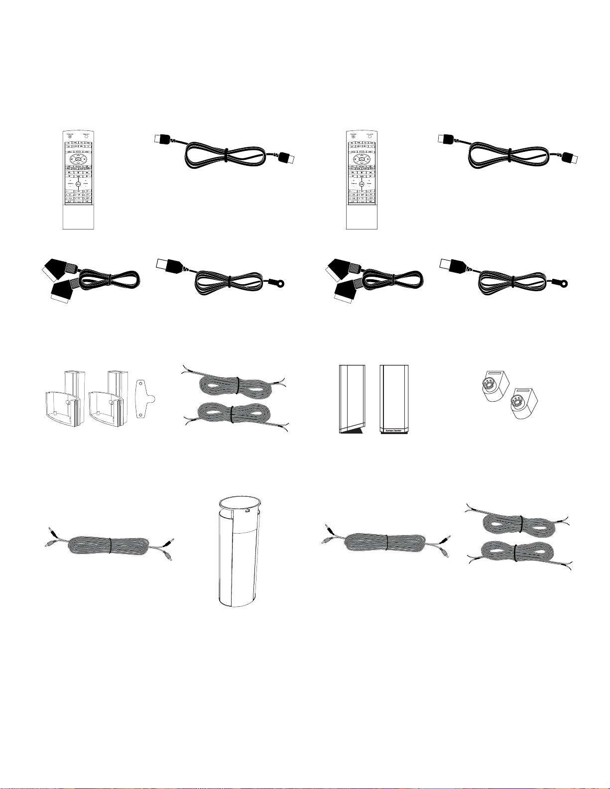
Supplied Accessories (for HS 280)
harman/kardon
HS 2X0/230 Service Manual
Page 3 of 73
Supplied Accessories (for HS 210)
The following accessory items are supplied with the HS 280 system.
If any of these items are missing, please contact Harman Kardon
Customer Service via www.harmankardon.com.
• System remote control • HDMI cable
• SCART cable • FM wire antenna
• Two speaker • Two five-meter (16.4-foot)
wall-mount brackets speaker cables
The following accessory items are supplied with the HS 210 system.
If any of these items are missing, please contact Harman Kardon
Customer Service via www.harmankardon.com.
• System remote control • HDMI cable
• SCART cable • FM wire antenna
• 2 TS-11 satellite speakers
• Two wall-mount brackets
• One combination LFE • 2 TS-60 Satellites
(low-frequency effects) and
trigger cable for connection to
the subwoofer
• Two five-meter (16.4-foot)
• One combination LFE
speaker cables
(low-frequency effects) and
trigger cable for connection to
the subwoofer
5
Page 4

Receiver Front-Panel Controls
Phones
Volume
EjectStandby
PRO LOGIC II
VIRTUAL
SPEAKER
DOLBY
DIGITAL
DOLBY
DIGITAL
Information
Display
Disc Slot Volume Control USB
Port
Headphone
Jack
Eject
Button
Standby
Button
Power
Indicator
TOP
FRONT SIDE
harman/kardon
HS 2X0/230 Service Manual
Page 4 of 73
Disc Slot: Insert a compatible disc into the slot. The HS 2X0SO/230’s
disc player will accept five-inch (12cm) and three-inch (8cm) discs.
Information Display: Various messages appear on this display in
response to commands. In addition, a variety of indicators will light at
various times to show the current source, settings or other aspects of
the HS 2X0SO/230’s status as described throughout this manual. See
Receiver Information Display, on page 7, for details.
Volume Control: Rotate the disc clockwise to raise the volume; rotate
counterclockwise to lower the volume. The volume level will appear
on the Information Display and on the on-screen menu (if the menu is
enabled, see Preferences – Volume Bar, on page 20).
Eject Button (on top of unit): Press this button to eject a disc from the
HS 2X0SO/230’s built-in DVD player. Before pressing this button, make
sure that no objects are blocking the disc slot. NOTE: If you do not
remove the ejected disc within 20 seconds, it will automatically re-load
back into the DVD player for protection.
Standby Button (on top of unit): This button turns the HS 2X0SO/230
on for playback or leaves it in the Standby mode for quick turn-on
using this button or the remote control.
Power Indicator: This LED (light-emitting diode) surrounds the Standby
switch. When the HS 2X0SO/230 is plugged into AC power, the LED
turns red to indicate that the HS 2X0SO/230 is in Standby mode (ready
to be turned on). When you turn the HS 2X0SO/230 on (by the Standby
switch or the remote control), the LED turns white.
Phones (headphones) Jack (on side of unit): Insert the 3.5mm stereo
mini-connector from a set of headphones into this jack. NOTE: When
a plug is inserted into the Phones jack, the HS 2X0SO/230’s speaker
outputs automatically mute; the HDMI audio output, coaxial output and
line output remain active.
USB 2.0 Port (on side of unit):
Gently insert a flash drive, card reader, digital camera or other USB
device, or a USB Standard-A cable connected to a USB device, to this
port.
IMPORTANT: DO NOT connect a PC or other USB host/controller to
this port, or you may damage both the HS 2X0SO/230 and your other
device.
Orient the other device’s plug so it fits all the way into the
HS 2X0SO/230’s USB connector. You may insert or remove the
device at any time — there is no installation or ejection procedure.
The HS 2X0SO/230 can play MP3 and Windows Media
®
Audio WMA
audio files that are stored on the device. The HS 2X0SO/230 can also
display JPEG-format still-image files.
6
Page 5

Receiver Information Display
VCD
Playback Control
Indicator
Playback
Mode
Indicators
Disc Type
Indicators
Random Play
Indicator
Title
Indicators
Chapter/Track Number
Indicators
Time
Indicators
Source
Indicators
Dolby Digital
Indicator
Repeat Play
Indicators
Progressive Scan
Indicator
Video Output
Indicators
Angle
Indicator
Video Format
Indicators
harman/kardon
HS 2X0/230 Service Manual
Page 5 of 73
Source Indicators: Indicate which source is currently playing.
Disc Type Indicators: Indicate the type of disc that is currently
playing.
Random Play Indicator: Indicates that the disc player is in the
Random Play mode.
Dolby Digital Indicator: Indicates that the soundtrack of the
currently-playing disc is Dolby Digital-encoded.
Progressive Scan Indicator: Indicates that the disc player is
outputting a progressive-scan video signal.
Repeat Play Indicators: Indicate that the disc player is in one of the
Repeat Play modes: Rep. = repeat all; Rep. 1 = repeat track;
A–B = A/B repeat.
Video Output Indicators: Indicate which type of video output is
currently active.
Angle Indicator: Indicates when alternative viewing angles are
available on the currently-playing DVD.
Video Format Indicators: Indicate which video format is currently
playing.
VCD Playback Control Indicator: Indicates that the playback-control
function is turned on when the HS 2X0SO/230 is playing a VCD.
Playback Mode Indicators: Indicate the current disc playback mode:
Indicates normal playback.
Indicates that the disc is in the forward fast-search mode.
The video display will indicate the selected speed.
Indicates that the disc is paused. The video display will also
indicate that the disc is paused.
Indicates that the disc is in the reverse fast-search mode.
The video display will indicate the selected speed.
Title Indicators: Show the title number of a DVD that is playing.
Chapter/Track Number Indicators: Show the current chapter when a
DVD is playing; show the current track number when a CD is playing.
Time Indicators: Show the running time when a DVD is playing; show
elapsed time when a CD is playing.
NOTE: The Title, Chapter/Track Number and Time Indicators will also
display the radio station name when Radio is the selected input. When
a DVD or CD is playing, the indicators will display various text messages about the disc’s status.
7
Page 6
MODEL: HS 2X0SO/230
Speaker
Outputs
Coaxial
Digital
Inputs
Optical
Digital
Inputs
Subwoofer
Output
Coaxial
Digital
Output
AC Power
Input
Sub
Tr igger
Output
Line
Outputs
Line 2
Inputs
SCART
Connection
FM
Antenna
Connection
Line 1
Inputs
Ethernet
Port
USB
Port
HDMI
Output
Composite
Video
Output
S-video
Output
Remote Control
Input/Output
Receiver Rear-Panel Connections
harman/kardon
HS 2X0/230 Service Manual
Page 6 of 73
See the Connections section, on page 14, for detailed information
about making connections.
AC Power Input: After you have made and confirmed all other
connections, plug the supplied AC power cord into this input and
into an unswitched AC outlet.
Speaker Outputs: Use the speaker wires supplied with the SAT TS60
speakers to connect the satellite speakers to the proper terminals.
Be sure to connect the positive (+, colored red) connector on the
speaker to the positive (+, colored red and white) connector on the
HS 2X0SO/230, and the negative (– , colored black) connectors on the
speakers to the negative (–, colored black) connectors on the
HS 2X0SO/230. See Connecting the Satellite Speakers, on page 14, for
more information about making connections.
Coaxial Digital Inputs: Connect the coaxial digital output of an
audio-only source component here. The signal may be a Dolby Digital
bitstream or a standard PCM digital audio bitstream.
NOTE: Use only one type of digital connection for each source
component.
Optical Digital Inputs: Connect the optical digital output of an
audio-only source component here. The signal may be a Dolby Digital
bitstream or a standard PCM digital audio bitstream.
NOTE: Use only one type of digital connection for each source
component.
Coaxial Digital Output: Connect this output to the coaxial digital input
of a digital recording device such as a CD-R or MiniDisc recorder.
Sub Trigger Output: Use the black mini-cable connector of the
supplied combination LFE and trigger cable to connect this jack to the
HKTS200SUB subwoofer’s External Trigger Input. See Connecting the
Subwoofer, on page15, for more details about making connections.
Whenever the HS 2X0SO/230 is turned on, it will send a trigger signal
that will turn the subwoofer’s amplifier on. Turning the HS 2X0SO/230
off removes the trigger signal, and the subwoofer’s amplifier will turn
off. (This change will occur even when the subwoofer’s Power On Mode
switch – see page 9 – is in the Auto position.)
Subwoofer Output: Use the LFE (purple) connector of the supplied
combination LFE and trigger cable to connect this jack to the
HKTS200SUB subwoofer’s Line-Level In LFE jack. See Connecting
the Subwoofer, on page 15, for more details about making connections.
Ethernet Port: Connect this port to your local area network (LAN) using
a CAT 5 RJ45 network cable. See Connecting to a Local Area Network
(LAN), on page 17, for details.
Line Outputs: Use the Line Outputs to connect to an audio-only recorder, such as a CD-R recorder or tape deck.
USB 2.0 Port: Gently insert a flash drive, card reader, digital camera
or other USB device, or a USB Standard-A cable connected to a USB
device, to this port.
IMPORTANT: DO NOT connect a PC or other USB host/controller to this
port, or you may damage both the HS 2X0SO/230 and the other device.
Orient the device’s plug so it fits all the way into the HS 2X0SO/230’s
USB connector. You may insert or remove the device at any time – there
is no installation or ejection procedure.
The HS 2X0SO/230 can display JPEG-format still-image files stored on
the device and can also play MP3 and Windows Media
files and MPEG4 and AVI video files that are stored on the device.
Line 1 Input/Line 2 Inputs: Use these inputs to connect to an
audio-only source component (such as a tape deck). Do not connect
a turntable to these jacks without a phono preamp.
®
Audio (WMA)
HDMI Output (HDMI version 1.2): If your video display is
HDMI-capable, connect it to the HS 2X0SO/230’s HDMI output for improved video performance. Since the HDMI cable transmits both video
and audio to the video display, we recommend that you disable your
display’s HDMI audio function to take full advantage of the
HS 2X0SO/230's system’s superior audio performance.
IMPORTANT: The HS 2X0SO/230 is in compliance with HDCP (High-Definition Copy Protection). A video display must also be HDCP-compliant
to be used with the HS 2X0SO/230’s HDMI output. For best results, we
do not recommend HDMI connections in excess of ten feet without a
repeater. If your video display has a DVI input, you may use an optional
HDMI-to-DVI cable or adapter for the video connection to the display.
(The DVI connection is video-only.)
8
Page 7
Remote Control Input/Output: If the HS 2X0SO/230’s front-panel IR
PL0004-01001
Subwoofer
Level Control
Bass Boost
Switch
Phase Switch
Power On
Mode Switch
External Trigger
Input Connector
Line-Level In
LFE Connector
Line-Level In
L/R Connectors
Power Switch
AC Power Cord
harman/kardon
HS 2X0/230 Service Manual
Page 7 of 73
sensor is blocked, such as when it is placed inside of a cabinet, connect an external IR receiver (such as the Harman Kardon HE 1000 – not
included) to the Remote Control In connector. You can then place the
external IR receiver in a location where it can receive the signals from
the HS 2X0SO/230 remote control.
You can connect the HS 2X0SO/230’s Remote Control Out connector to
the remote IR input of a compatible device, allowing it to be controlled
through the HS 2X0SO/230 (and through an external IR receiver, if
connected). You can even connect several such compatible devices
together in “daisy-chain” fashion.
SCART Connection: Connect it to a compatible TV or set-top box
using the included SCART cable. The SCART cable carries composite
(CVBS) video or S-Video from the HS 2X0SO/230 to a TV or set-top box
(as well as a control signal for automatically controlling picture aspect
ratio and other parameters). It also carries stereo audio from the
TV or set-top box back to the HS 2X0SO/230.
Composite-Video Output: Connect it to the composite-video input
of a TV or video projector.
S-Video Output: Connect it to the S-Video input of a TV or
video projector.
FM Antenna Connection: Connect the supplied FM antenna to
this terminal.
Subwoofer Controls and Connections
Although in most cases the Phase Switch should be left in the Normal
position, there is no absolutely correct setting for it. When the
subwoofer is properly in phase with the satellite speakers, the sound
will be clearer and have maximum impact. It will make percussive
sounds like drums, piano and plucked strings sound more lifelike.
The best way to set the Phase Switch is to listen to music that you
know well and set the switch in the position that gives drums and other
percussive sounds maximum impact.
Power On Mode Switch: When this switch is set in the Auto
position and when the Power switch is set to On, the HKTS200SUB
will automatically turn itself On whenever it receives an audio signal.
It will enter the standby mode if it receives no audio signal for 20
minutes. When the Power On Mode switch is set in the On position, the
subwoofer will remain on whether or not it is receiving an audio signal.
An LED on the subwoofer’s top panel indicates whether the subwoofer
is in the on or standby mode:
• When the LED is illuminated blue, the subwoofer is turned on.
• When the LED is not illuminated, the subwoofer is in standby mode.
When the Power switch is set to Off, the LED will not be illuminated,
no matter what setting the Power On Mode switch is in.
External Trigger Input Connector: Use the mini-plug of the supplied
combination LFE and trigger cable to connect the External Trigger Input
to the trigger output of another compatible component. Whenever the
subwoofer detects a trigger signal between 3V and 30V (AC or DC), the
subwoofer’s amplifier will turn on. The subwoofer’s amplifier will turn
off after the trigger signal ceases. (This change will occur even when
the Power On Mode switch is in the Auto position.)
Line-Level In LFE Connector: Use the LFE (purple) connector of
the supplied combination LFE and trigger cable to connect the
Line-Level In LFE connector to the dedicated subwoofer output of a
receiver or preamp/processor. This input bypasses the subwoofer’s
internal crossover circuitry, so use it only with a subwoofer output that
is low-pass filtered. (Check the receiver or preamp/processor’s
documentation to confirm that its subwoofer output is low-pass
filtered.) If your receiver or preamp/processor does not have a
dedicated subwoofer output that is low-pass filtered, use the
subwoofer’s Line-Level In L/R connectors instead.
Subwoofer Level Control: Use this control to adjust the HKTS200SUB
subwoofer’s volume. Turn clockwise to increase the volume; turn
counterclockwise to decrease the volume.
Bass Boost Switch: Set this switch to On to enhance the subwoofer’s
low-frequency performance. Set this switch to Off for normal
low-frequency performance.
Phase Switch: This switch determines whether the subwoofer driver’s
piston-like action moves in and out in phase with the satellite
speakers. If the subwoofer were to play out of phase with the satellite
speakers, the sound waves from the satellite speakers could cancel out
the sound waves from the subwoofer, reducing bass performance and
sonic impact. This phenomenon depends in part on the relative
placement of all the speakers in the room.
Line-Level In L/R Connectors: Use these connectors if your receiver
or preamp/processor does not have digital surround-sound decoding
or a low-pass-filtered subwoofer output.
• If your receiver or preamp/processor has a separate subwoofer
output, use the LFE (purple) connector of the supplied combination
LFE and trigger cable to connect the receiver or preamp/processor’s
subwoofer output to either one of the subwoofer’s Line-Level In L/R
connectors.
• If your receiver or preamp/processor does not have a separate
subwoofer output, use two Y-adapters (not supplied). Connect one
adapter’s single end to the unit’s preamp output for that channel.
Connect one of this adapter’s dual ends to the main amp input for
that channel, and connect the adapter’s other dual end to one of the
subwoofer’s Line-Level In L/R Connectors. Repeat this process with
the other Y-adapter, the preamp channel, the main amp input and the
subwoofer’s other Line-Level In L/R connector.
Power Switch: Set this switch in the On position to turn the subwoofer
on. The subwoofer will then either be on or in Standby mode, depending on the setting of the subwoofer’s Power On Mode switch.
AC Power Cord: After you have made and verified all subwoofer and
speaker connections described in this manual, plug the Power Cord into
an active, unswitched electrical outlet (that is, an outlet not connected
to a light switch) for proper operation of the subwoofer. DO NOT plug
this cord into the accessory outlets found in some audio components.
9
Page 8
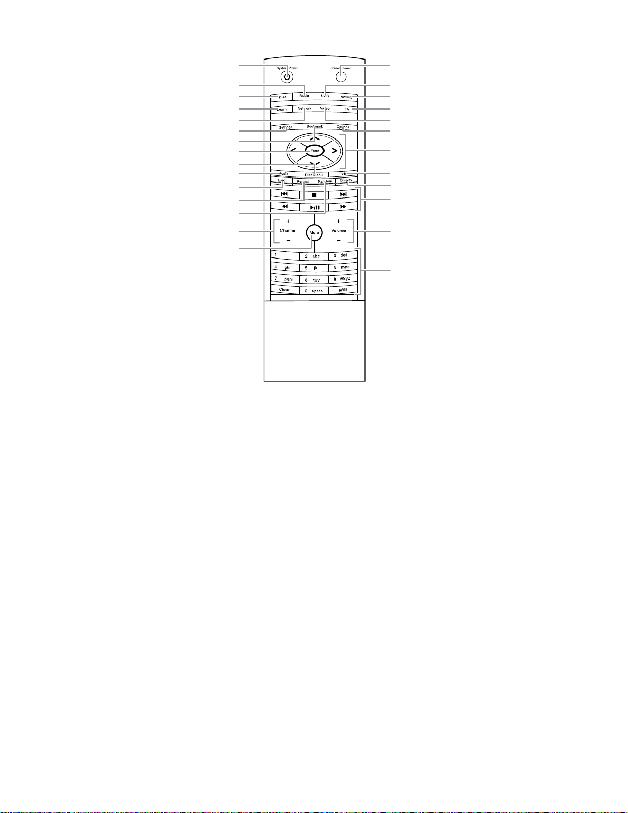
Remote Control Functions
System Power
Button
Radio Button
Disc Button
Screen Power
Button
USB Button
Activity Button
TV Button
Video Button
Learn Button
Disc Menu Button
Mute Button
Network Button
Settings Button
Bookmark Button
Eject Button
Channel + / –
Buttons
Repeat Button
Random Button
Volume + / –
Buttons
Options Button
Cursor Controls
Enter Button
Audio Button
Exit Button
Display Button
Disc Transport
Buttons
Numeric Buttons
harman/kardon
HS 2X0/230 Service Manual
Page 8 of 73
System Power Button: Switches the HS 2X0SO/230 into the Standby mode.
Screen Power Button: Switches your video display on and off.
Disc Button: Selects the HS 2X0SO/230’s built-in DVD player as the
system’s active sound source and plays a disc that has been inserted into
the player. Pressing this button also puts the remote control into the disc
player control mode. See Using the DVD Player, on page 21, for details.
NOTE: Pressing this button when the HS 2X0SO/230 is in the Standby mode
will switch it on.
Radio Button: Selects the HS 2X0SO/230’s built-in FM radio as the
system’s active sound source. Pressing this button also puts the remote
control into the control mode for the radio. See Using the FM Tuner, on
page 23, for details. NOTE: Pressing this button when the HS 2X0SO/230
is in the Standby mode will switch it on.
USB Button: Selects a device connected to the front- or rear-panel USB
ports as the system’s active sound source. The HS 2X0SO/230’s on-screen
menu system lets you navigate through the files stored on the device. See
Playing Files from USB Devices, on page 24, for details. NOTE: Pressing this
button when the HS 2X0SO/230 is in the Standby mode will switch it on.
Activity Button: Switches the on-screen menu to the Activity menu from
any other active screen or menu. See Activity Button, on page 21,
for details. NOTE: Pressing this button when the HS 2X0SO/230 is in the
Standby mode will switch it on.
Learn Button: Places the remote control in the learning mode. See
Programming the Remote Control, on page 17, for details.
Network Button: Switches to the local area network (LAN) that is
connected to the HS 2X0SO/230’s rear-panel Network connector. See
Playing Files from Networked Devices, on page 25, for details. NOTE:
Pressing this button when the HS 2X0SO/230 is in the Standby mode will
switch it on.
Video Button: Puts the remote control into the video-control mode,
allowing it to control a video source component with codes that you
have programmed into the remote. See Programming the Remote
Control, on page 17, for details. If you have designated one of the
HS 2X0SO/230’s analog-audio inputs as a video-component audio input,
pressing the Video button will also make that input the system’s
active sound source. See Connecting Audio Sources/Line 1, Line 2 In,
on page 16, for details.
TV Button: Puts the remote control into the TV-control mode,
allowing it to control your TV or video display with codes that you have
programmed-into the remote. See Programming the Remote Control,
on page 17, for details. If you have designated one of the HS 2X0SO/230’s
analog-audio inputs as the TV-audio input, pressing the TV button will
also make that input the system’s active sound source. See Connecting
Audio Sources/Line 1, Line 2 In, on page 16, for details.
Settings Button: Displays the HS 2X0SO/230’s Settings menu. See
Settings Menu, on page 19, for details.
Bookmark Button: Displays the list of your stored bookmarks for easy
access. See Bookmarks, on page 21, for details.
Options Button: Displays any available options for a menu item that
is selected in the on-screen menu.
Cursor Controls: Use these controls – the up cursor, down cursor, left
cursor and right cursor – to navigate through items on the on-screen
menu.
Enter Button: Press it to select items highlighted on the on-screen menu.
Audio Button: Lets you select from the different listening modes that are
available for the source that you have selected. Pressing the Audio button
while you are playing a DVD will display the on-screen audio-mode menu.
10
Page 9
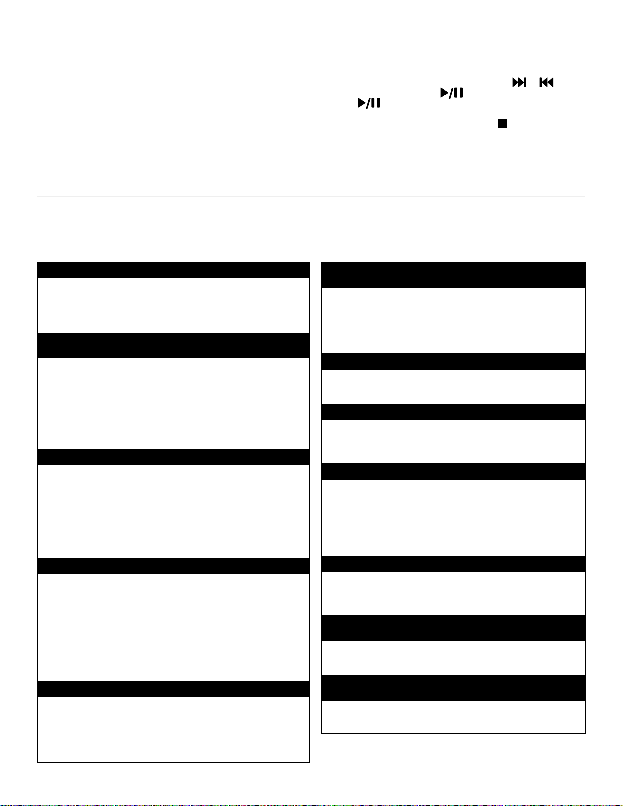
If there are other MP3s in the folder with the one that you've selected,
harman/kardon
HS 2X0/230 Service Manual
Page 9 of 73
the HS 2X0SO/230 will play each one, in order as they appear on the
OSD screen.
• To skip to the next or previous MP3 file, press the or
button. To pause play, press the button. To resume play,
press the button again.
• To exit and return to file list screen, press the button.
Playing Videos
Selecting a video file plays the file. If there are other video files in the
folder, the HS 2X0SO/230 will play each one, in order as they appear
on the OSD screen.
Troubleshooting
If your HS 2X0SO/230 system isn’t performing the way you think it should, check to see if the problem is covered in this section
before calling your dealer or contacting Harman Kardon.
The receiver won’t power up (the Power Indicator is not lit): There is noise or other interference in the picture while the HS 280
• Check that the receiver’s AC Power Cord is properly plugged into
the receiver’s AC Power Input connector.
• Check that the AC power cord is plugged into a working AC outlet
and that the AC outlet is not controlled by a switch.
Sound plays through the HS 2X0SO/230 speakers, but there is no
TV picture:
• Check the connection between the receiver and the TV.
• Check that the T V is turned on and is set to the proper input source.
• Confirm that all of the choices made in the Settings: Video menu are
correct for your T V.
• If you’re using the HDMI connection, be sure that the TV or video
display is HDCP-compliant. If the TV is not HDCP-compliant,
disconnect the HDMI cable and use the receiver’s S-Video or
composite-video connection.
There is no sound coming from the subwoofer:
• Check that the subwoofer’s power cord is plugged into a
working AC outlet.
• Check that the subwoofer’s Power Switch is in the on position.
• Check that the Subwoofer Level Control is not turned all the way
down (fully counterclockwise).
• Check the audio connection between the receiver and the subwoofer.
• Check the receiver’s Settings: Audio: Subwoofer menu to make sure
that the subwoofer volume has not been set at -10dB.
There is a constant hum in the sound:
is playing a DVD:
• Check that the disc surface is clean and not scratched.
• If you have the receiver’s video output connected to your TV
through your VCR, the copy-protection program on some DVDs
could affect picture quality. Connect the receiver’s video output
directly to your TV’s video input.
The sound and picture are out of sync:
• Check the Audio: Settings : Delay menu and change the Delay
setting to put the sound back in sync with the picture.
The HS 2X0SO/230 cannot tune in radio stations:
• Check that the FM antenna is correctly connected.
• Adjust the antenna’s position. If necessary, use a powered
FM antenna or an outdoor FM antenna.
The receiver does not respond to remote control commands:
• Replace all three of the remote control’s batteries with fresh ones,
and make sure to install them correctly.
• Hold the remote control closer to the receiver.
• Check that the receiver’s remote sensor is in line of sight with
the remote control. If necessary, use an optional Harman Kardon
HE 1000 external IR receiver.
The remote does not control programmed components (TV or Video):
• Check that all input cables are plugged all the way into their
connectors.
• Check that all cables are at least 3m (9.8 ft.) from fluorescent lights.
• Check that all cable connectors are clean. If necessary, wipe them
with a cloth slightly moistened with alcohol.
• Turn the subwoofer’s Power switch off. If the hum goes away,
there is a ground loop between the subwoofer and the receiver.
Plugging the subwoofer’s Power Cord into the same AC outlet that
the receiver is plugged into should eliminate the ground loop.
The disc does not play:
• Check that the disc is inserted correctly (label-side up) .
• Check that the disc is the correct type: DVD, DVD-R, DVD-RW,
DVD+ R / R W, VCD, SVCD, CD, C D-R / RW, MP3, WMA (v7 and v8 ).
Other disc types will not play.
• Check that the disc surface is clean and not scratched.
• Check that you have pressed the remote’s T V or Video button
before trying to operate the component.
• Re-learn the component’s commands into the remote.
The Ø symbol appears on the screen when you press a remote
control button:
• The selected function is not permit ted at the time the but ton
is pressed.
The receiver does not respond to commands, or behaves in an
erratic way:
• Unplug the receiver’s power cord from the AC outlet,
wait 30 seconds, then plug it back in.
You can find additional troubleshooting information in the FAQs link
on the Support page at www.harmankardon.com.
27
Page 10

Specifications
harman/kardon
HS 2X0/230 Service Manual
Page 10 of 73
HS 2X0SO/230 Receiver
Audio Section
Continuous ave rage power, s tereo mode (FTC ):
65 watts per channel, 120Hz–20kHz,
@ <0.3% THD, both channels driven into 6 ohms
Input sensitivity/impedance (line inputs): 240mV/47k ohms
Frequency response @ 1W (±3dB): 120Hz–20kHz
Transient intermodulation distortion (TIM): <0.2%
FM Tuner Sec tion
Frequency range: 87.5 – 108.0MHz
Usable sensitivity IHF: 3.0μV/14.7 dBf
Signal-to-noise ratio (mono/stereo): 65dB/60dB
Distor tion mono/stereo : 0.3%/0.5%
Stereo separation: 40dB @ 1kHz
Selectivity ± 400kHz: 65dB
Image rejection: 40dB
IF rejection: 70dB
DVD Player Section
Supported disc format s: 5-inch (12cm) or 3-inc h ( 8cm) DV D V ideo, DV D-Audio,
stand ard-con fo rmi ng DV D- R, DVD +R, DV D- RW, D VD +RW, VCD, C D, CD-R , C D- RW,
MP3 (up to 320kbps bitrate), or WMA (v7-v8) discs
Region code: 2
DVD layers: Single-side/single-layer, single-side/dual-layer, dual-side/dual-layer
Audio for mats : D olby Digital, lin ear P CM , M P3 ( up to 320kbps bit rate) ,
Windows Media 7 or 8
Still-image format : JPEG
Video signal system: NTSC or PAL
Composite-video output: IV p-p/ 75 ohms, sync negative polarity
S-Video output : Y/luminance: IV p-p/75 ohms, sync negative polarit y;
C/chrominance: 0.3V p-p
Freque ncy resp onse: DVD (linear PCM ): 20 Hz –2 2k Hz, ±1.0dB,
CD: 20Hz–22kHz ±1.0dB
Signal-to-noise ratio: 90dB ( A-weighted)
Dynamic range: DVD/CD : 92dB (16-bit)
THD/1kHz: DVD/CD : 0.01%
Wow & flutter: Below measurable limits
Video Section
Television format: Automatic or PAL (selectable)
Output level/impedance: 1.0Vp-p/75 ohms
Video frequency response : (composite and S-Video) 10Hz–8MHz ( –3dB)
HDMI™ version : 1.2
General
Power requirement: AC 100–240V ~ 50/ 60Hz
Power consumption : 300W maximum, 1W standby
Dimensions Unit Shipping
Height 98mm (3-7/8 inches) 197mm (7-3/4 inches )
Width 350mm (13-25/32 inches ) 484mm (19-1/16 inches)
Depth 280mm (11 inches) 355mm (14 inches)
Weight: 3.5kg (7.7 lb) 6.1kg (13.4 lb)
Depth mea surement in cludes termina l connec tions . H eight measuremen t
includes feet and chassis.
Speaker System
Frequency response: 45Hz–20kHz ( -6dB)
SAT TS60 Satellites ( for HS 280)
Recommended power: 10 ~ 120 wat ts
Impedance: 8 ohms nominal
Sensitivity: 86dB @2.83V/1 meter
Tweeter: One 19mm ( 3/4") dome, video-shielded
Midrange: Dual 75mm (3" ) flat-panel drivers, video-shielded
Dimensions:
Height 299mm (11-25/32 inches)
Width 110mm (4-11/32 inches)
Depth 88mm (3-15/32 inches )
Weight : 1.5kg (3.3 lb )
Height measurement includes removable stands.
SAT-TS11 Satellites ( for HS 2 10)
Recommended power: 10 ~ 120 wat ts
Impedance: 8 ohms nominal
Sensitivity: 86dB @ 2.83V /1 meter
Tweeter: One 1/ 2" (12mm) dome, video-shielded
Midrange: Dual 3" ( 75mm) drivers, video-shielded
Dimensions:
Height 243mm (9-9/ 16 inches)
Width 100mm (3-15/16 inches)
Depth 92mm (3-5/8 inches )
Weight: 1kg (2.2 lb)
HKTS200SUB Subwoofer
Input rating: AC 220 –240V~, 50/ 60Hz, 200W
Amplifier power: 200 watts RMS
Woofer: 8" cone in a sealed enclosure
External trigger input voltage: 3 ~ 30 volts AC/DC
Dimensions (H x W x D ):
Height 353mm (13-29/32 inches )
Width 267mm (10-1/2 inches)
Depth 26 7mm (10 -1/2 inches )
Weight : 9kg (19.8 lb )
Height measurement includes the product’s feet.
Features, specifications and appearance are subject to change without notice.
31
Page 11
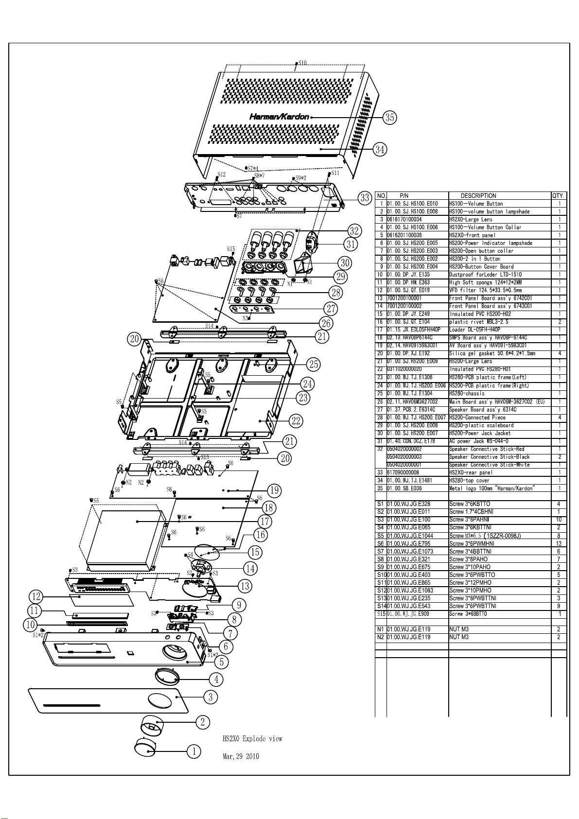
harman/kardon
HS 2X0/230 Service Manual
Page 11 of 73
Please note:
Item 18, SMPS Board Assembly has part
number 0209HAV08P6144C2X0.
Page 12
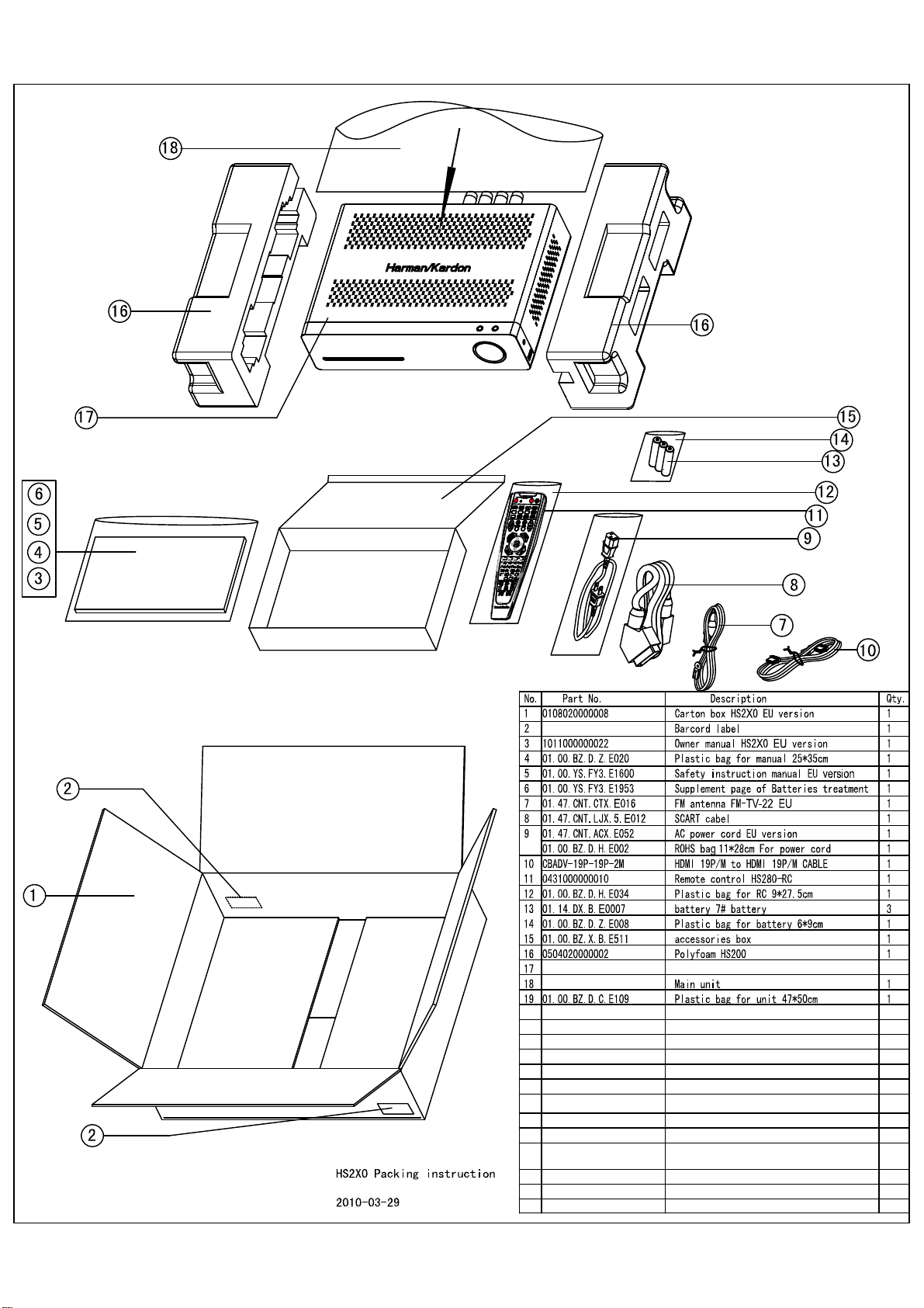
harman/kardon
HS 2X0/230 Service Manual
Page 12 of 73
Page 13
Item P/N Description Specification QtyLocation.No. Note
g
p
)
p
)
5
k
5
d
k
k
k
k
A
2
s
W
A
pray
A
pray
A
pray
A
(
)
4
p
4
A
6
p
y
6
C
7
p
t
7
A
A
go)
p
6
p
8
AC p
k
g
p
g
)
g
A
g
)
φ
)
ponge
)
p
pong
t
s
2
0
y)
2
(
(1)
(3)
)
w
(1)
w
)
(4)
(4)
(4)
w
)
w
)
p
)
w
)
w
)
t
)
t
)
)
p
)
(
)
(
)
(
)
y
A
x
s
8
x
0
y
pp
n
2
n
p
k
p
e
0
0
k
A
y
g
g
g
g
g
g
g
g
g
g
g
8
harman/kardon
HS 2X0/230 Service Manual
Page 13 of 73
1 01.00.WJ.TJ.E1304 metals part HS280-chassis 1 HS280-PT01
2 01.00.WJ.TJ.E1481 metals part HS280-top cover 1 HS280-PT07
3 617090000008 metals part HS2X0-rear panel 1 HS280-PT02
4 01.00.WJ.TJ.E1306 metals
5 01.00.WJ.TJ.HS200.E006 metals
6 01.00.WJ.TJ.HS200.E007 metals part
7 01.00.WJ.TJ.E1307 Heatsin
8 01.00.WJ.TJ.E1336 Heatsin
9 01.00.WJ.TJ.E892 Heatsin
10 01.00.WJ.TJ.E893 Heatsink
11 01.00.WJ.TJ.E268 Heatsin
12 01.00.WJ.TJ.E1379 Heatsink HS280 Heatsink-2, W24*H11*L23MM, 1 HS280-PT06, For U6,U17 on Mainboard
13 030200000000
14 0616201100038 plastic part HS2X0-front panel 1 HS200-RE01
15 01.00.SJ.HS200.E002 plastic part HS200-2 in 1 Button 1 HS200-RE02
16 01.00.SJ.HS200.E003 plastic part HS200-Open button collar 1 HS200-RE03
17 01.00.SJ.HS100.E006 plastic part HS100-Volume Button Collar 1 HS100-RE06
18 01.00.SJ.HS200.E00
19 01.00.SJ.HS200.E005 plastic part HS200-Power Indicator lampshade 1 HS200-RE05
20 01.00.SJ.HS200.E00
21 01.00.SJ.HS200.E00
22 01.00.SJ.HS200.E008 plastic part HS200-plastic scaleboard 1 HS200-RE08
23 0616170100034 plastic part HS2X0-Large Lens 1 HS200-RE10
24 01.00.SJ.HS100.E010 plastic part HS100-Volume Button 1 HS100-RE10
25 01.00.SJ.HS100.E008 plastic part HS100-volume button lampshade 1 HS100-RE08
26 01.00.SJ.1000A.E01
27 01.00.SJ.QT.E019 VFD filter 124.5*33.5*0.5mm 1 material is as DVD22
28 01.40.CON.DCZ.E17
29 01.00.SB.E036 Metal lo
30 01.00.DP.JY.E135 Dust
31 01.00.DP.XJ.E192 Silica gel gasket
32 0305010000003 Diathermanous Selenium Rubber
33 01.00.DP.HM.E359 sponge
34 01.00.FZ.QT.153 Astigmatism PVC Φ45.5*Φ9.5mm 1
35 01.00.FZ.QT.E253 Mask PVC
36 01.00.DP.HM.E364 s
37 01.00.DP.HM.E378 High Soft sponge 124*10*2MM (with Single side glued) 1
38 01.00.DD.PM.E271 electric s
39 01.00.FZ.QT.E122 Plastic fastener 12CM 1 For power cord fastnes
40 01.00.DP.QT.E113 Sil-pad sil-pad 400-302
41 031102000002
42 01.00.DP.JY.E249 Insulated PVC HS200-H0
43 01.00.DP.JY.E541 Insulated PVC 22.5*10*0.3mm
44 01.00.WJ.JG.E328 Screw M3*6KBTTO 5
45 01.00.WJ.JG.E543 Screw M3*6PWBTTNI 9 For pedestal underlay and chissis (9)
46 01.00.WJ.JG.E235 Screw M3*8PWBTTNI 5
47 01.00.WJ.JG.E011 Scre
48 01.00.WJ.JG.E100 Screw M3*8PAHNI 10
49 01.00.WJ.JG.E472 Scre
50 01.00.WJ.JG.E085 Screw M3*6KBTTNI 2 For front panel and volume button board(2)
51 01.00.WJ.JG.E1044 Screw 1SZZR-0098J(M3*6.5,LG Appointed) 8
52 01.00.WJ.JG.E795 Screw M3*6PWMHNI 13
53 01.00.WJ.JG.E909 Screw M3*6BBTTO 1 For U type connect piece and rear panel(1)
54 01.00.WJ.JG.E1073 Screw M3*4BBTTNI 6
55 01.00.WJ.JG.E321 Scre
56 01.00.WJ.JG.E675 Scre
57 01.00.WJ.JG.E403 Screw M3*6PWBTTO 5
58 01.00.WJ.JG.E865 Scre
59 01.00.WJ.JG.E1083 Scre
60 01.00.WJ.JG.E119 Nu
61 01.00.WJ.JG.E119 Nu
62 01.00.WJ.JG.E426 Flat Pad M3*0.5 W=8 2 For Heatsink and AV Board (2
63 01.00.SJ.QT.E104 plastic rivet MBL3-2.5 2
64 01.00.WJ.JG.E424 S
65 0504020000002 Speaker Terminal Connector
66 0504020000001 Speaker Terminal Connector
67 0504020000003 Speaker Terminal Connector
68 01.00.DP.QT.E558 Pol
69 01.00.BZ.X.B.E511
70 010802000000
71 01.00.YS.FY3.E1600 Safet
72 01.00.YS.FY3.E1953 Su
73 101100000002
74 01.00.YS.TZ.T.E068 Laser label Laser
75 01.00.YS.TZ.T.E057 Laser label Laser
76 043100000001
77 01.14.DX.B.E0007G
78 01.00.BZ.D.S.E109 Plastic ba
79 01.00.BZ.D.Z.E020 Plastic ba
80 01.00.BZ.D.Z.E034 Plastic ba
81 01.00.BZ.D.Z.E008 Plastic ba
82 01.00.BZ.D.H.E002 ROHS ba
83 01.47.CNT.LJX.5.E211 HDMI Cord CBADV-S05-2 1 Outsourcin
84 01.47.CNT.ACX.E052 Power Cord
85 01.47.CNT.LJX.5.E05
art HS280-PCB bracket(Left
art HS200-PCB bracket(Right
Magnetism annulu
lastic part HS200-Button Cover Board 1 HS200-RE0
lastic part HS200-pedestal underla
lastic part HS200-Power Jack Jacke
lastic part 1000A-IR receiver support 5.5mm 1
ower Jac
o 100mm "Harman/Kardon" Thin Logo 1 For top cover
roof for Disc tray door of Loder LTD-1510 1 Black
e 20*20*10MM 1 Between front panel PCB and plastic par
Insulated PVC HS280-H01 (transparenc
ring Pad M3 2 For Heatsink and AV Board (2
foam HS200 1
ccessories bo
Carton bo
and Warning instruction manual Harman/Kardon EU Version 1
lement page of Batteries treatmentA4 paper Size 1 12 Kinds of languages, Harman/Kardo
Owner manual HS2X0(HS280&HS210) EU Versio
Remote control RC-HS28
lkalescent batter
for unit 47*50cm 1 For unit Packin
Connect cable scart 1.5m 1 EU Vision
HS200-Connected Piece for
Speaker Jack
HS280-Amplifier Heatsink 1 HS280-PT0
HS280-Power Heatsin
35*30*49mm 1 HS200-PT10 For SMPS Board
16*12*51MM (The Hole's depth is 18MM)
28*28*10mm 1 For U21 on Mainboard
F5BRH12*27*5.6-P.
WS-044-0 1 EU Version
50.6*4.2*1.5mm (with #500 glue be single
sides
lued
Gap Pad VO UItra
Soft,L15*W8*T0.3,sin
20*10*7MM (with #9448 glue be double
sides
lued
38.5 (Underside Glued
10*10*7MM (with double sides glued
M1.7*4CBHNI 1 For Button cover Board and button Board
M3*8PBTTNI 7 For ICs and Heatsinks on SMPS Board (7
M3*8PAHO 7 For output jacks (7
M3*10PAHO 2 For plastic scaleboard and rear panel (2
M3*12PMHO 2 For AC power socket (2
M3*10PMHO 2 For SCART Jack (2
M3 2 For SCART Jack (2
M3 2 For power jack2
H-HS2 copper Terminal Connector-Red
Surface gilded
H-HS2 copper Terminal Connector-Black
Surface gilded
H-HS2 copper Terminal Connector-White
Surface gilded
HS200 340*170*45mm 1 For accessorie
HS2X
recausion mar
recausion guid
GP7# 3
25*35cm 1 For Owner manual Packin
9*27.5CM 1 For Remote Control Packin
6*9cm 1 For battery Packin
11*28cm 1 For power cord packin
WS-002E+WS-019 HO5VV-F 0.75×2C BK
2M
le sides glued
with Single side glued)6 For hamulus of front panel
1 HS280-PT03 1.0mm galvanized sheet
1 HS200-PT0
4 HS200-PT06
1 HS280-PT04 For SMPS Board
For S503/S504/S505/S506 on SMPS
4
Board
2 For Amplifier Output Cord
2 HS200-RE0
1 HS200-RE0
4 For pedestal underlay HS100-H01
Between U407 and Amplifier Heatsink on
1
V board
2 For VFD(2)
Between volume button and Front Panel
Board
1 Inside the volume button Black PVC
1 For IR receiver
paste in front of Disc tray door in the front
anel
1 For Q509 on SMPS Board
1 For SMPS Board
1 Be buckled above volume button board
For front Panel and Left/Right sides of
chassis (4), Between two Heatsinks on
SMPS Board
For front panel and pedestal underlay and
chissis
; For AV Board and Heatsink (2
For front panel and front panel board(9)
For plastic scaleboard and Speaker
Connected Board
For Loader and chassis(4), For PCB
Brackets and chassis
For SMPS Board and chassis (5), For AV
Board and chassis (4), For Main Board and
PCB brackets
For rear panel and the bottom side of
chassis (2), For top cover and bottom side
of chassis
For top cover and chassis, top cover and
rear
anel (5
For Insulated gasket and volume button
Board
1
2
1
1
1
1
1
1 Outsourcing, Blac
1 EU Vision
0.8mm galvanized sheet,
natural color
0.55mm galvanized and precoated sheet, black color
EU Version, 0.6mm
alvanized sheet
Upon the U407 on AV Boar
luminium alloy, Oxidation,
Black
ntiflaming, ABS,94V0;
Black Color and S
BS, Appointed Color and
S
technique
BS, Appointed Color and
S
technique
BS, Spray argent color
Same as HS100
BS, Black
transparent ABS+dispersion
material
transparent PV
ntiflaming ABS,94V0, Black
BS, Black, For Speaker
Connected Board
Mitsubishi
3mm Black Lens (Include
47mm “harman/kardon”
Lo
Rubber Lacquer Appointed by
client
Transparent ABS +
dis
ersion material
Black
EU Vision
EU Vision
White
Match for DVD21
HS2X0 Component List
Page 14

Item P/N Description Specification Qty Location.No. Note
harman/kardon
HS 2X0/230 Service Manual
Page 14 of 73
86 01.47.CNT.CTX.E016 Antenna
87 01.15.JX.EDL05MHEA Loader DL-05MH-H40P(EA) 1 Foryou,Mabuchi EA motor
88 01.47.CNT.LJX.7.E603 Connect cable
89 01.47.CNT.LJX.7.E706 Connect cable
90 0804020100006 Connect cable
91
01.48.BPX.1.E147 Flat cable 1.0*14P*100mmA 2
92 01.48.BPX.1.E148 Flat cable 1.0*8P*100mmA 1
93 01.48.BPX.1.E149 Flat cable 1.25*12P*80mmA(T=0.1mm) 1
94 01.48.BPX.1.E151 Flat cable 1.0*24P*80mmA 1
95 01.48.BPX.1.E167 Flat cable 1.0*20P*80mmA 1
96 01.48.BPX.1.E153 Flat cable 1.25*14P*70mmA(T=0.1mm) 1
97 01.48.BPX.1.E154 Flat cable 1.0*6P*40mmA 1
98 01.48.BPX.1.E155 Flat cable 1.25*9P*60mmA(T=0.1mm) 1
99 01.48.BPX.1.E156 Flat cable 1.0*12P*220mm
100 01.48.BPX.1.E028 Flat cable 0.5*24P*200mmA 1 For Loader and CN2 on Main Boar
101 01.37.PCB.2.E6314C Speaker Connected Boar
02.11HAV09M5982C01 Mainboard (semi-manufactured goods)
102
103 02.14HAV09I5983C01 AV Board (semi-manufactured goods HAV09I-5983C01 (EU Vision 1
104 0219HAV08P6144C2X0 SMPS Board (semi-manufactured
105 7001200100001
106 7001200100002
Front Panel Board (semi-manufactured
goods)
Volume Button Board (semimanufactured goods)
d 6314C 1 2-layers
FM-TV-22 (Lead content less than
300PPM)
VH-3Y Connector-2Y-120mm(Be same
side)
VH-3Y Connector-2Y-2Y-60mm(Be same
side)
NSCL-20090908-01,VH-4Y Connector-4P
80mm(Be same side with color is White,
Black, Red and Black)
A 1 For Loader and CN9 on Main Board
HAV09M-5982C01 (EU Vision+Hitachi
Loader)
goods) HAV08P-6144 1 2-layers. Power supply board.
6742C 1 2-layers
6743C 1 2-layers
1 EU Vision
CN501 on SMPS Board to Power Jack with
1
solder one end
CN506 on SMPS Board to CN400(L) on AV
1
Board
-
CN406 on AV Board to JP1.JP2 on
1
Speaker Connected Board with solder one
end
CN4(A) on Mainboard to CN601(A) on
Front Panel Board*1, CN5(D) on
Mainboard to CN403(D) on AV board*1
CN2(B) on Mainboard to CN603(B) on
Front Panel Board
CN3(C) on Mainboard to CN504(C) on
SMPS Board
CN1(E) on Mainboard to CN401(E) on AV
Board
CN6(F) on Mainboard to CN404(F) on AV
Board
CN503(H) on SMPS Board to CN602(H) on
Front Panel Board
CN604(J)on Front Panel Board to
CN605
(J) on Volume Button Board
CN505(K) on SMPS Board to CN405(K) on
AV Board
1 4-layers
2-layers
d
HS2X0 Component List for Mainboard (5982C)
HS2X0 Component List
Item P/N Description Specification Qty Location.No. Note
1 01.57.R.2.E000J Resistor, chip 0603-0Ω ±5% 19
2 01.57.R.2.E020J Resistor, chi
3 01.57.R.2.E100J Resistor, chip 0603-10Ω±5% 2 (R22) (R92)
4 01.57.R.2.E220F Resistor, chip 0603-22Ω±1% 1 R286
01.57.R.2.E220J Resistor, chip 0603-22Ω±5% 42
5
6 01.57.R.2.E330J Resistor, chi
7 01.57.R.2.E430J Resistor, chip 0603-43Ω±5
8 01.57.R.2.E49R9F Resistor, chip 0603-49.9Ω±1% 10
9 01.57.R.2.E680F Resistor, chip 0603-68Ω±1% 3 R229 R250 R254
01.57.R.2.E750F Resistor, chip 0603-75Ω±1% 10
10
11 01.57.R.2.E820F Resistor, chip 0603-82Ω±1% 2 R20 R252
12 01.57.R.2.E101J Resistor, chip 0603-100Ω±5% 14
13 01.57.R.2.E271J Resistor, chi
14 01.57.R.2.E301J Resistor, chip 0603-300Ω±5% 1 R178
01.57.R.2.E331J Resistor, chip 0603-330Ω±5% 3 R45 R103 R10
15
16 01.57.R.2.E391J Resistor, chip 0603-390Ω±5% 1 R134
01.57.R.2.E471J Resistor, chip 0603-470Ω±5% 3 R156 R157
17
18 01.57.R.2.E511F Resistor, chip 0603-510Ω±1% 1 R285
01.57.R.2.E102F Resistor, chip 0603-1KΩ±1
19
20 01.57.R.2.E102J Resistor, chip 0603-1KΩ±5% 6 (R51) (R52) R61 R62 (R275) R194
21 01.57.R.2.E152J Resistor, chip 0603-1.5KΩ±5% 2
22 01.57.R.2.E162J Resistor, chi
01.57.R.2.E182J Resistor, chip 0603-1.8KΩ±5% 2 (R267) (R269)
23
24 01.57.R.2.E222J Resistor, chip 0603-2.2KΩ±5% 1 (R276)
25 01.57.R.2.E332J Resistor, chip 0603-3.3KΩ±5% 2 (R271) (R272)
26 01.57.R.2.E472J Resistor, chip 0603-4.7KΩ±5%
27 01.57.R.2.E103J Resistor, chip 0603-10KΩ±5%
28 01.57.R.2.E123F Resistor, chip 0603-12KΩ±1% 3 (R2) R37 R155
29 01.57.R.2.E1212F Resistor, chi
30 01.57.R.2.E153J Resistor, chip 0603-15KΩ±5% 3 R163 R210 R209
31 01.57.R.2.E203J Resistor, chip 0603-20KΩ±5% 1 R152
32 01.57.R.2.E223F Resistor, chip 0603-22KΩ±1% 1 (R1)
33 01.57.R.2.E393J Resistor, chip 0603-39KΩ±5% 1 R167
01.57.R.2.E473J Resistor, chip 0603-47KΩ±5% 5 R144 R147 R175 R176 R26
34
35 01.57.R.2.E104J Resistor, chip 0603-100KΩ±5% 15
36 01.57.R.2.E105J Resistor, chip 0603-1MΩ±5% 2 (R168
37 01.57.R.3.E000J Resistor, chip 0805-0Ω ±5
38 01.57.R.3.E4R7J Resistor, chip 0805-4.7Ω±5% 2 (R154) (R153)
39 01.57.R.8.EP2204 Resistor, thick film chip network
40 01.57.R.8.EP3304 Resistor, thick film chip network 0603-33Ω*4 ±5% 8
41 01.57.R.Y.E270 Voltage Dependent Resistor, TDK AVR-M1608C270MTABB SMD 2 ESD3 ESD2
42 01.57.R.R.E050 Thermal Dependent Resistor, JinKe JK-MSMD050 SMD 1 PTC1
43 01.54.CS.2.E150N50V Capacitor, multilayer ceramic, chip 0603-15P NPO±5%/50
44 01.54.CS.2.E200N50
45 01.54.CS.2.E151N50V Capacitor, multilayer ceramic, chip 0603-150P NPO±5%/50V 2 C128 C129
46 01.54.CS.2.E681N50
47 01.54.CS.2.E122X50V Capacitor, multilayer ceramic, chip 0603-122 X7R±10%/50V 1 C108
01.54.CS.2.E152X50V Capacitor, multilayer ceramic, chip 0603-152 X7R±10%/50V 1 C123
48
49 01.54.CS.2.E332X50V Capacitor, multilayer ceramic, chip 0603-332 X7R±10%/50V 1 C109
50 01.54.CS.2.E392X50V Capacitor, multilayer ceramic, chip
51 01.54.CS.2.E103Y50V Capacitor, multila
52 01.54.CS.2.E103XT50V Capacitor, multilayer ceramic, chip 0603-103 X7R±5%/50V 1 (C15)
53 01.54.CS.2.E223X50V Capacitor, multilayer ceramic, chip 0603-223 X7R±10%/50V 1 (C76)
V Capacitor, multilayer ceramic, chip 0603-20P NPO±5%/50V 6 (C70) (C68) (C119) (C127) (C20) (C21
V Capacitor, multilayer ceramic, chip 0603-680P NPO±5%/50V 2 C97 C120
p 0603-2Ω±5% 1 R21
p 0603-33Ω±5% 6
p 0603-270Ω±5% 1 (R139)
p 0603-1.6KΩ±5% 1 R177
p 0603-12.1KΩ±1% 1 (R131)
yer ceramic, chip 0603-103 Y5V-20+80%/50V 6 C3 (C6) (C8) C74 C75 (C111)
% 1 (R24)
% 1 R19
% 1 R132
0603-22Ω*4 ±5% 22
V 1 (C241)
0603-392 X7R±10%/50V 1 (C239)
R146 R158 R159 R160 R162 R164 R165
(R198) R227 R233 R235 R266 R268 R281
R59 R278 R279 R280 (R291)
R29 R30 R35 (R39) R42 R56 R63 R64 R65
R68 R73 R74 R75 R82 R83 R84 R105
R106 R107 R108 R109 R112 R113 R114
R115 R116 R123 R124 R125 R183 R184
R185 (R224) R195 R246 R40 R78 R79
R141 R186 R190 R196
R55 R57 R60 R143 R208 R259
(R93) (R94) (R95) (R96) (R212) (R213)
(R214) (R215) R216 R21
R228 R231 R234 R240 R241 R244 R245
R253 R206 R211
R46 R230 R236 R237 (R238) R264 R265
(R282) (R283) R58 (R151) (R150) R179
R180
(R101) (R102)
(R3) (R6) (R7) (R10) (R11) (R13) (R15)
R18 R25 R26 R27 R28 R43 (R44) R47 R5
32
R69 (R71) R72 R85 R86 R87 R88 R89
(R126) (R133) R135 R138 (R182) (R242)
R261 R14
0
(R91) (R97) (R98) (R99) (R110) (R117)
R136 R137 R148 R149 R161 R166 R169
22
R170 R171 R172 (R197) R218 R219 R220
(R222) R270
R9 R31 R32 (R33) R34 R38 R49 R66 R67
R90 R192 R203 R205 R207 (R41)
) (R36)
RN2 RN3 RN4 RN5 RN6 RN8 RN10 RN12
RN14 RN24 RN27 RN29 RN30 RN31
RN33 RN34 RN35 RN36 RN37 RN38
RN39 RN40
RN19 RN21 RN22 RN23 RN25 RN26
RN28 RN32
7
4
(R239)
2
3
)
Page 15
Item P/N Description Specification QtyLocation.No. Note
V
p
V
V
p
V
8
V
p
V
)
V
p
V
5
V
p
V
5
V
p
V
V
p
V
5
V
p
C
C
0
C
8
C
7
D
2
2
3
D
2
E
4
y
p
Ω
)
p
Ω
p
Ω
)
(
D
y
D
8
A
3
8
)
r
r
6
r
r
r
-
y
P
C
P
5
0
3
A
8
A
A
p
r
0
8
A
)
g
2
r
)
)
A
8
_NL(
)
g
)
p
(
)
W
)
K
)
(
)
g
A
w
y
p
)
8
k
D
D
5
r
r
5
k
A
A
k
k
)
j
2
5
h
3
r
2
r
t
g
0
r
r
3
r
g
7
h
yp
e
p
s
harman/kardon
HS 2X0/230 Service Manual
Page 15 of 73
54 01.54.CS.2.E104Y50V Capacitor, multilayer ceramic, chip 0603-104 Y5V-20+80%/50V 133
55 01.54.CS.2.E474X10
56 01.54.CS.2.E105X16
57 01.54.CS.2.E104Y50V Capacitor, multilayer ceramic, chip 0603-104 Y5V-20+80%/50V 54
58 01.54.CS.2.E475X16
59 01.54.CS.3.E106X16
60 01.54.CS.3.E335Y16
61 01.54.CS.3.E475X16
62 01.54.CS.B.E1023K
63 01.35.CC.E120622U10
64 01.34.CL.D.E10U16V
65 01.34.CL.D.E22U16V
66 01.34.CL.D.E47U10V
67 01.34.CL.D.E47U16V
68 01.34.CL.D.E100U10V
69 01.34.CL.D.E100U16VC Capacitor, AL.electrolytic CD110-100UF/16V 5*11 17
70 01.34.CL.D.E220U16VD Capacitor, AL.electrolytic CD110-220UF/16V 6.3*12 7 CE7 CE8 CE31 CE33 CE35 CE36 CE38
71 01.34.CL.D.E470U10V
72 01.34.CL.D.E1000U10V
73 01.38.FUSE.S.EJK110 Pol
74 01.13.L.Z.ESA50 Bead, chip 0603-50Ω 10
75 01.13.L.Z.ESA120 Bead, chi
76 01.13.L.Z.ESB50 Bead, chip 0805-50Ω 11
77 01.13.L.Z.ESB220 Bead, chi
78 01.13.L.Z.ESC50 Bead, chi
79 01.13.L.Z.ED50A Bead, leaded fixed
80 01.13.L.L.S.E007 Inductor, multilayer ceramic, chip 0805-10UH SMD 12
81 01.13.L.L.S.E320 Inductor, SMD SPI1048QR-150
82 01.13.L.L.S.E242 Inductor, multila
83 01.41.D.PS.EB340L
84 01.41.D.PD.E539
85 01.41.D.PS.ELL414
86 01.41.D.PS.EBAV99 Diode
87 01.42.Q.S.E1132 Transisto
88 01.42.Q.S.ET3904 Transisto
89 01.42.Q.S.E2N390
90 01.42.Q.S.EC8550 Transisto
91 01.42.Q.S.E8050 Transisto
92 0218020000007 Crystal Oscillator
93 01.00.JZ.E27000 Quart
94 01.00.JZ.E24000
95 01.44.IC.D.EL780
96 01.46.IC.EK4S561632JUC60 IC, Samsung , SDRAM K4S561632J-UC60(TSOP54,256M,SMD) 1 U7
97 01.46.IC.EK4S643232HUC6
98 01.44.IC.S.EA11173V
99 01.44.IC.S.EA11171V
100 01.44.IC.S.E1117 IC, AAC, LDO
101 01.44.IC.S.EMP1411DH IC,MPS,Ste
102 01.46.IC.EAML821
103 01.46.IC.EFLI2310 IC, ST, Di
104 01.46.IC.ETMD8809X0
105 01.46.IC.EK9F1G08UOB IC, Samsung, Flash
106 01.46.IC.EW25X16VSSIG IC, Winbond, Flash W25X16VSSIG(SOIC-8,SMD
107 01.46.IC.EW9812G6GH IC, Winbond, SDRAM W9812G6GH-6 SMD,54L-TSOP2-400mil 1 U19
108 01.44.IC.S.EAM5888 IC, AMtek, Motor Driver
109 01.44.IC.S.EFMS6143 IC, Fairchild, Video Filter Driver FMS6143CSX
110 01.46.IC.ESII9034CTU IC, Silicon Ima
111 01.44.IC.D.EPC817 IC, Shar
112 01.46.IC.EUSB2514AEZG IC, SMSC, USB HUB Controller USB2514-AEZG
113 01.46.IC.ESN74ALVC244P
114 01.46.IC.ESN74AUP1G80DC
115 01.46.IC.ELAN8700CAEZG IC, SMSC, Ethernet Transceiver LAN8700C-AEZG
116 01.44.IC.S.E3522 IC, Analo
117 01.44.IC.S.E0514
118 01.46.IC.EMK900 IC, Multek, Lisence Chi
119 01.44.IC.S.EFST3257MTC
120 01.40.CON.DCZ.E316 HDMI Jac
121 01.13.L.R.E13
122 01.40.CON.DDZ.EDSW-30 S-Vidio Connecto
123 01.40.CON.DCZ.E04
124 01.40.CON.DCZ.E857 RJ45 Jac
125 01.40.CON.DCZ.E217 USB Jac
126 01.40.CON.DCZ.E203 IR in/out
127 01.40.CON.S10.FPC1.E01
128 01.40.CON.S13.FPC2.E00
129 01.40.CON.S10.FPC2.E00
130 01.40.CON.S10.FPC2.E03
131 01.40.CON.S10.FPC2.E031 FPC Connecto
132 01.40.CON.S10.FPC2.E00
133 01.40.CON.S05.E00
134 01.00.WJ.TJ.HS650.E002 Metal Part HS650DL-U t
135 01.37.PCB.4.E5982C
Capacitor, multilayer ceramic, chi
Capacitor, multilayer ceramic, chi
Capacitor, multilayer ceramic, chi
Capacitor, multilayer ceramic, chi
Capacitor, multilayer ceramic, chi
Capacitor, multilayer ceramic, chi
Capacitor, multilayer ceramic, chi
Capacitor, multilayer ceramic, chi
Capacitor, AL.electrolytic CD110-10UF/16V 5*11 2 CE12 CE41
Capacitor, AL.electrolytic CD110-22UF/16V 5*11 6 CE51 CE52 CE56 CE48 CE49 CE5
Capacitor, AL.electrolytic CD110-47UF/10V 5*11 5 CE3 CE6 CE29 CE46 CE5
Capacitor, AL.electrolytic CD110-47UF/16V 5*11 3 CE14 CE16 CE1
Capacitor, AL.electrolytic CD110-100UF/10V 5*1
Capacitor, AL.electrolytic CD110-470UF/10V 6.3*1
Capacitor, AL.electrolytic CD110-1000UF/10V 8*1
er Positive Temperature Coefficent JK-110(1.1A) SMD 1 PTC3
Diode B340LA SMD 1 D1
Diode IN5393 DIP 3 D5 D10 D11
Diode LL4148 SMD 1 D4
Transisto
Quartyz Crystal Unit 24.000MHZ-49S-20
IC, ST, Voltage Regulator L7805,TO-220 1 U22
IC, Samsung , SDRAM K4S643232H-UC60(TSOP86,64M,SMD)1 U31
IC, AAC, LDO
IC, AAC, LDO
IC, Amlogic, A/V Processor
IC, TAMUL, MPEG Processo
IC, TI, Octal Buffer with 3-State outputs SN74ALVC244PW(TSSOP-20,SMD
IC, TI, D-Type FLIP-FLOP SN74AUP1G80DCK(SC-70,SMD
IC, Semtech, Lo
Diode Arra
IC, Fairchild, Multiplexer/Demultiplexer
Bus Switch
Ethernet Transforame
Jac
FPC Connector, SMD FPC-1.0-12P with upward touc
FPC Connecto
FPC Connecto
FPC Connecto
FPC Connecto
FPC connector, SMD FPC-0.5-24P with upward touc
PCB Board-Mainboard without
com
er ceramic, chip, TDKACM2012-900-2P SM
z Crystal Unit 27.000MHZ-49S-20
-Down Converte
ital Video Format Converter FLI2310-LF-CF,PQFP-208,SMD 1 U21
e, HDMI Transmitter SII9034CTU(TQFP-100,SMD
, Photoelectric Coupler PC817 DIP 1 U14
Tech., Reset Circuit
Capacitance TVS
ack CKX-3.5-2
onent
0603-474 X7R±10%/10
0603-105 X7R±10%/16
0603-475 X7R ±10%/16
0805-106 X7R±10%/16
0805-335 Y5V-20+80%/16
0805-475 X7R±10%/16
1812-102/3K
ECJMFF1A226Z 1 C64
0603-120
0805-220
1206-50
50Ω(3.5*6.0*0.8)
15uH/3A) SM
BAV99LT1,SOT23 (or
LBAV99L1G,SOT23
2SB1132,SOT89 2 Q5 Q6
MMBT3904,SOT23 1 Q3
2N3906,SOT23 1 Q2
KTC8550,SOT23 3 Q1 Q4 Q7
KTC8050,SOT23 1 Q10
7050 OSC-50.000MHz,50.000MHz,
25PPM~+25PPM,3.3V,SMD
Z1117H-3.3,SOT-223 3 U1 U4 U11
Z1117H-1.8,SOT-223 2 U2 U23
Z1117H-ADJ,SOT-223 1 U3
MP1411DH,MSOP-1
ML8218(PQFP-216,SMD
TMD8809X02(160-LQFP-2424,SMD
K9F1G08UOB-PCBO SMD,48-TSOP11220F
M5888 SMD,HSOP2
AT3522 SMD,SOT-23 1 U5
RClamp0514M SMD,MSOP-10L 4 U25 U26 U27 U30
MK-900(SOP14,MCU,SMD
FST3257MTC SMD 1 U36 FAIRCHILD
1747981-1 SM
13F-38ANL SMD 1 U35
DSW-30 1 JP5
V1-8.4-8G 1 JP6
26LM90-37121-01 1 JP1 Yilian
USB-A-05 (ROHS, Mother Set
1.25-12P Vertical Type and Dual Conact1 CN3 Black
1.0-8P Vertical Type and Dual Conac
1.0-14P Vertical Type and Dual Conact2 CN5 CN4 Black
1.0-20P Vertical Type and Dual Conact1 CN6 Black
1.0-24P Vertical Type and Dual Conact1 CN1 Black & Antiflamin
5982C 1
SOIC-8,SMD
QFN-36,SMD
QFN-36,SMD
e connect piec
C1 (C2) C4 (C5) C7 C9 (C10) C11 (C12)
(C13) (C14) (C16) C17 C18 C19 (C22)
C23 (C24) C25 C26 C27 (C28) (C29) (C30)
(C31) (C32) (C33) (C34) (C35) (C36) (C38)
(C40) (C41) (C42) (C43) (C44) C45 (C46)
(C47) (C48) (C49) (C50) (C51) (C52) (C53)
C54 (C55) (C56) (C57) (C58) C59 C61
(C65) (C66) (C71) (C72) (C73) C79 C82
C83 (C84) (C85) (C86) (C88) (C89) C90
C91 C92 C93 C94 (C96) (C98) C99 (C100)
(C101) (C102) C103 (C105) C106 (C107)
C110 C112 C113 C114 C115 (C116)
(C117) (C118) (C121) (C124) (C125)
(C126) C130 C131 C132 C133 (C134)
C135 C136 (C138) (C139) (C140) C141
(C142) (C143) (C144) (C145) (C146)
(C147) C148 (C149) (C150) (C151) (C152)
(C153) (C154) (C155) C160 C163 C164
C165 C166 C167 C168 C169 C170 C171
C172 C173 (C174) C175 C176 C177
1 C122
5(C60) C62 C63 (C104) C23
C178 (C179) C180 (C181) (C182) (C183)
(C184) (C185) (C186) (C187) (C188)
(C189) (C190) (C191) (C192) (C193)
(C194) C195 (C198) C199 (C200) (C201)
(C202) (C203) C204 (C205) (C206) (C207)
(C208) (C209) (C210) (C211) (C212)
(C213) (C214) (C215) (C216) (C217)
(C218) (C219) (C220) (C221) (C222)
(C223) (C224) (C225) (C230) C231 C232
C233 (C234) C236 (C237) C240
1(C37
4 C87 C228 C229 C23
2 C244 C24
1 C243
2 C69 C9
6 CE1 CE2 CE9 CE47 CE57 CE6
CE4 CE10 CE11 CE15 CE18 CE19 CE20
CE21 CE32 CE34 CE37 CE39 CE40 CE42
CE60 CE61 CE6
1 CE13
1 CE30
FB6 FB23 FB24 FB25 FB16 FB17 FB18
FB20 FB41 FB44
1(FB22
FB8 (FB9) FB10 FB11 (FB12) (FB14)
FB39 FB19 FB26 FB42 FB43
1 FB21
4 FB7 FB37 FB38 (FB40
FB1 FB2 FB3 FB4 FB5 FB13 FB15 FB27
10
FB35 FB36
(L1) L2 (L3) L4 L5 L6 L8 L9 L10 L11 L13
L14
1 L19
4 L15 L16 L17 L1
3 D12 D13 D14
1Y3
2 Y2 Y4
1Y5
1 U28
1U6
1 U17
1 U9 firmware burn-in
1 U18 firmware burn-in
1 U15
1 U20
1 U24
1 U32
1 U29
1U8
1 U12
1 U34 Burn code: MK90
1 JP7 51UO19S-331N-A SM
ntiflaming, Yellow Color
1 JP4
2 JP2 JP3
1 CN9
1 CN2 Black & Antiflamin
1 CN10
1H1
HS2X0 Component List for Mainboard (5982C)
Page 16
Item P/N Description Specification QtyLocation.No. Note
p
%
p
%
p
%
5
p
%
0
p
%
9
p
%
7
p
%
3
p
%
7
p
%
p
%
5
p
%
5
p
%
p
%
p
%
0
p
%
p
%
0
p
%
3
p
%
p
%
p
%
2
p
%
8
p
%
p
%
4
9
)
V
p
V
V
p
V
V
p
V
V
p
V
6
V
p
V
V
p
V
0
6
V
p
V
7
V
p
V
)
V
p
V
8
V
p
V
)
V
p
V
)
V
p
V
5
V
p
V
9
V
p
V
9
3
p
V
V
p
V
)
V
p
V
C
7
C
3
5
C
6
C
5
8
D
2
C
3
D
2
2
H
A
7
p
r
T
V
5
-
)
p
Ω
A
8
-
y
M
-
8
r
r
8
5
V
(
)
(
)
g
g
A
4
D
4
r
5
0
r
r
3
r
g
p
pins
r
g
2
A
g
A
g
k
p
g
k
p
s
harman/kardon
HS 2X0/230 Service Manual
Page 16 of 73
HS2X0 Component List for AV Board (5983C)
1 01.57.R.1.E000J Resistor, chi
2 01.57.R.1.E220J Resistor, chi
3 01.57.R.1.E101J Resistor, chi
4 01.57.R.1.E202J Resistor, chi
5 01.57.R.1.E472J Resistor, chi
6 01.57.R.2.E000J Resistor, chip 0603-0Ω ±5% 24
7 01.57.R.2.E100J Resistor, chi
8 01.57.R.2.E561J Resistor, chi
9 01.57.R.2.E750F Resistor, chi
10 01.57.R.2.E101J Resistor, chi
11 01.57.R.2.E111J Resistor, chi
12 01.57.R.2.E471J Resistor, chi
13 01.57.R.2.E751F Resistor, chi
14 01.57.R.3.E221F Resistor, chi
15 01.57.R.2.E102J Resistor, chi
16 01.57.R.2.E162F Resistor, chi
17 01.57.R.2.E222J Resistor, chi
18 01.57.R.2.E332J Resistor, chi
19 01.57.R.2.E472J Resistor, chi
20 01.57.R.2.E622F Resistor, chi
21 01.57.R.2.E103J Resistor, chi
22 01.57.R.2.E473J Resistor, chi
23 01.57.R.2.E104J Resistor, chip 0603-100KΩ±5% 7 4R19 4R24 R459 R460 R466 R468 R469
24 01.57.R.4.E102J Resistor, chi
25 01.57.R.4.E202J Resistor, chi
26 01.57.R.Y.E270 Voltage Dependent Resistor, TDK AVR-M1608C270MTABB SMD 8
27 01.57.R.C.E220 FIXED CARBON FILM
28 01.54.CS.1.E103X50
29 01.54.CS.1.E104X10
30 01.54.CS.1.E223X25
31 01.54.CS.2.E180N50
32 01.54.CS.2.E270N50
33 01.54.CS.2.E331N50
34 01.54.CS.2.E103X50V Capacitor, multilayer ceramic, chip 0603-103 X7R±10%/50V 9
35 01.54.CS.2.E104Y50V Capacitor, multilayer ceramic, chip 0603-104 Y5V-20+80%/50V 25
36 01.54.CS.2.E104X50
37 01.54.CS.2.E333X50
38 01.54.CS.2.E473X50
39 01.54.CS.3.E102N50
40 01.54.CS.3.E103X50
41 01.54.CS.3.E104X50
42 01.54.CS.3.E475X16
43 01.54.CS.3.E106X16
44 01.54.CS.3.E226X6V
45 01.54.CS.4.E104X50
46 01.54.CS.4.E105X50
47 01.34.CL.D.E10U10V
48 01.34.CL.D.E10U16V
49 01.34.CL.D.E470U6V
50 01.34.CL.D.E22U16V
51 01.34.CL.D.E47U10V
52 01.34.CL.D.E47U25VC1 Capacitor, AL.electrolytic CD110-47UF/25V 5*11 2 CE417 CE42
53 01.34.CL.D.E100U10V
54 01.34.CL.D.E100U16V
55 01.34.CL.D.E330U16V
56 01.34.CL.D.E1000U50V
57 01.33.CT.EA3U310V
58 01.00.CD.DL.E474100
59 01.13.L.L.S.E434 Inductor, SMD
60 01.13.L.Z.ESA50 Bead, chi
61 01.13.L.Z.ESB50 Bead, chip 0805-50Ω 6 FB408 FB411 FB413 FB414 FB415 FB416
62 01.13.L.Z.ED50
63 01.13.L.L.D.E127 Magnetic shielding Inductor 983BN-1003-15UH 4 L401 L402 L403 L404
64 01.00.JZ.E20250 Quart
65 01.00.JZ.E32768Y Crystal Oscillator 32.768KHZ 3.3V 5*3.2mm SMD 1 Y403
66 01.41.D.PS.ELL414
67 01.41.D.PS.EBAV99 Diode BAV99LT1 SMD 2 D403 D402
68 01.42.Q.S.E8050 Transisto
69 01.42.Q.S.EC8550 Transisto
70 01.42.Q.S.EDTC343 Transistor DTC343TKT146 SMD 7 Q401 Q402 Q406 Q407 Q408 Q410 Q411
71 01.44.IC.D.EL780
72 01.44.IC.S.EC5FP
73 01.46.IC.EMAP5601ME5900
74 01.46.IC.ETAS5352DD
75 01.46.IC.ESI4705B20GM
76 01.44.IC.S.EFST3257MTC
77 01.44.IC.S.E3522 IC, Analo
78 01.44.IC.S.EV330 IC, TI, Video Switch FSAV330 SMD 1 U409
79 01.46.IC.EW25X80SS IC, Winbon, Flash W25X80-SS SMD 1 U410
80 01.46.IC.E74H0
81 01.40.CON.S13.FPC2.E00
82 01.40.CON.S10.FPC2.E03
83 01.40.CON.S10.FPC2.E031 FPC Connecto
84 01.40.CON.S10.FPC2.E00
85 01.40.CON.DCZ.E244 Connector
86 01.40.CON.DCZ.E129 Connector
87 01.43.E011
88 01.40.CON.DCZ.E203 Jack, YuanChan
89 01.40.CON.DCZ.E865 Jack H-AV2-8.4-9PB-14 1 JP406
90 01.40.CON.DCZ.E864 Jack H-AV8-8.4-13PB-54 1 JP403
91 01.40.CON.DCZ.E181 Jack, YuanChan
92 01.57.R.R.E010 Thermal De
93 01.40.CON.DCZ.E863 Jack, Hon
94 01.37.PCB.2.E5983C
Capacitor, multilayer ceramic, chi
Capacitor, multilayer ceramic, chi
Capacitor, multilayer ceramic, chi
Capacitor, multilayer ceramic, chi
Capacitor, multilayer ceramic, chi
Capacitor, multilayer ceramic, chi
Capacitor, multilayer ceramic, chi
Capacitor, multilayer ceramic, chi
Capacitor, multilayer ceramic, chi
Capacitor, multilayer ceramic, chi
Capacitor, multilayer ceramic, chi
Capacitor, multilayer ceramic, chi
Capacitor, multilayer ceramic, chi
Capacitor, multilayer ceramic, chi
Capacitor, multilayer ceramic, chi
Capacitor, multilayer ceramic, chi
Capacitor, multilayer ceramic, chi
Capacitor, AL.electrolytic CD110-10UF/10V 5*11 2 CE426 CE42
Capacitor, AL.electrolytic CD110-10UF/16V 5*11 1 CE421
Capacitor, AL.electrolytic
Capacitor, AL.electrolytic CD110-22UF/16V 5*11 4 CE408 CE414 CE415 CE41
Capacitor, AL.electrolytic CD110-47UF/10V 5*11 2 CE425 CE40
Capacitor, AL.electrolytic CD110-100UF/10V 5*1
Capacitor, AL.electrolytic CD110-100UF/16V 5*11 4 CE418 CE420 CE422 CE42
Capacitor, AL.electrolytic CD110-330UF/16V 6.3*1
Capacitor, AL.electrolytic GF102M050I250
Solid Electrolyte Tantalum Chip
Ca
acito
Capacitor, polyester film 474J/100V DIP 2 C472 C45
Bead, leaded fixed
z Crystal Unit 20.250MHz-49S 18P/±20PP
Diode LL4148 SMD 2 D400 D401
IC, ST, LDO
IC, Rohm, LDO
IC, Micronas, Audio Processor
IC, TI, Stereo Digital Amplifier
IC, Silicon labs, FM Radio Receiver
IC, Fairchild, Analo
IC, TI, Hex Inverter 74HCU04 SM
FPC Connecto
FPC Connecto
FPC Connecto
Jack, Sharp, Fiber optic iuput jack with
shutte
PCB board-AV Board without
com
onent
Switch
ic Tech, Reset monitor
, SUB Tirgger JackCKX-3.5-2
, SCART Jac
endent Resistor, JinKeJK-MSMD010 SMD 1 PTC400
Chang, FM Jac
0402-0Ω±5
0402-22Ω±5
0402-100Ω±5
0402-2KΩ±5
0402-4.7KΩ±5
0603-10Ω±5
0603-560Ω±5
0603-75Ω±1
0603-100Ω±5
0603-110Ω±5
0603-470Ω±5
0603-750Ω±1
0805-220Ω1
0603-1KΩ±5
0603-1.6KΩ±1
0603-2.2KΩ±5
0603-3.3KΩ±5
0603-4.7KΩ±5
0603-6.2KΩ±1
0603-10KΩ±5
0603-47KΩ±5
1206-1KΩ±5
1206-2KΩ±5
CR1/2WT/B22Ω±5%(RT,22Ω,±5%,1/2W,DI
P
0402-103 X7R±10%/50
0402-104 X7R ±10%/10
0402-223 X7R±10%/25
0603-18P NPO±5%/50
0603-27P NPO±5%/50
0603-330P NPO±5%/50
0603-104 X7R±10%/50
0603-333 X7R±10%/50
0603-473 X7R±10%/50
0805-102 NPO±5%/50
0805-103 X7R±10%/50
0805-104 X7R±10%/50
0805-475 X7R±10%/16
0805-106 X7R±10%/16
0805-226 X7R±20%/6.3
1206-104 X7R±10%/50
1206-105 X7R±10%/50
470uF/6.3V 6.3*12 ±20% 10
A-3.3UF-10V 1 CA400
CS0603-R27J-S(0603,270NH,±2%,High
frequency,SMD
0603-50
50Ω(3.5*6.0*0.
KTC8050 SMD 1 Q400 SOT23
KTC8550 SMD 3 Q404 Q405 Q409 SOT23
L7808C-V DIP, TO-220 1 U405
BA00HC5FP SMD, T0252-
MAP5601M-E5-900(PMQFP-128-2,SMD) 1 U403
TAS5352DDV
SI4705-B20-GM
FST3257MTC SMD 1 U411
1.25-9P Vertical Type and Dual Conact1 CN40
1.0-14P Vertical Type and Dual Conact1 CN403 Black
1.0-20P Vertical Type and Dual Conact1 CN404 Black
1.0-24P Vertical Type and Dual Conact1 CN401 Black & Antiflamin
Vertical VH Connector with four holes and
four
Vertical VH Connector with three holes and
two
GP1FAV51RK0F 2 JP405 JP404
CS-101 1 JP401 Fully Shield
IF-02P 1ANT401 nickel-plate
5983C 1 2-layers
HTSSOP-44,SMD
AT3522 SMD,SOT-23 1 U406
ins
℃
)
QFN-36,SMD
1 4R38
5 4R31 4R32 4R39 4R40 4R41
2 4R33 R42
2 4R29 4R3
1 4R53
4R06 4R08 4R09 4R11 4R12 R441 R442
R443 R445 4R45 R446 4R49 R453 R454
R455 R456 R457 R461 R462 R463 R464
4R52 4R51 R44
4 4R43 4R44 4R46 4R4
2 4R17 4R2
3 4R25 4R20 R42
1 R467
2 R428 R43
6 R472 R477 R479 R481 R483 R48
1 R431
2 R436 R401
4 R419 R405 R408 R41
1 R415
3 4R18 4R26 4R5
5 R407 R409 R412 R413 R42
2 4R28 4R21
1 R429
6 R414 R417 R418 R420 R421 R42
3 4R22 4R27 4R4
1 R406
2 R403 R40
ESD401 ESD402 ESD405 ESD406
ESD407 ESD408 ESD410 ESD40
2 R438 R437
1 C400
1 C490
1 C487
2 C415 C41
1 C410
6 C420 C422 C424 C426 C428 C43
C432 C440 C441 C442 C443 C479 C483
C484 C48
C401 C402 C407 C408 C411 C414 C417
C431 C433 C434 C435 C436 C437 C438
C439 C444 C445 C446 C447 C480 C481
C482 C485 4C02 C403
6 C453 C454 C463 C469 C473 C49
4(C493) (C494) (C495) (C496
3 C404 C405 C41
4(C450) (C459) (C466) (C476
4(C451) (C460) (C467) (C477
4 C458 C465 C474 C47
6 C419 C421 C423 C425 C427 C42
4 4C00 C406 C498 C49
1 4C05
4(C448) (C462) (C464) (C478
4 C461 C468 C470 C471
1 CE419
1 CE402
2 CE411 CE41
3 CE400 CE406 CE40
1 L405
2 FB405 FB406
1 FB409
1 Y400 SJK
1 U404
1 U407
1 U408
1 U401 TSSOP14
1 CN406 White & Antiflaming
1 CN400 White & Antiflaming
1 JP402
CAPXON
Can Replaced by
T491A335K016A
FaLa, XiaMen
Can Replaced by THI1315
150
Can Replaced by 5032 OSC
0.032768MHZ,32.768KHZ,±2
5PPM,3.3V,SMD
Can Replaced by
LBAV99L1G SMD
Can Replaced by SGM330A
SMD
Can Replaced by A25L080MF/G, firmware burn-in
Black
ntiflaming; The color of two
terminals is Oran
ntiflaming; The color is
Orange, White, White&White
from left to right on top line
and Purple, Red, Red&Red
from left to right on bottom
line.
e.
Page 17
Item P/N Description Specification QtyLocation.No. Note
p
%
5
p
%
p
%
p
%
9
p
%
p
%
p
%
0
8
p
%
7
p
%
3
p
%
4
p
%
6
p
%
4
p
%
p
%
p
%
p
%
p
%
p
%
6
p
%
p
%
7
p
%
4
p
%
2
p
%
5
p
%
4
5
K
r
p
r
6
0
e
V
p
V
V
p
V
V
p
V
V
p
V
V
p
V
0
V
p
V
V
p
V
V
p
V
V
p
Z
V
V
V
A
)
A
)
5
V
)
V
)
V
)
3
V
)
)
D
A
5
D
A
4
2
H
A
7
V
A
A
,
)
r
7
r
P
2
8
(
)
g
r
)
H
6
A
)
(
)
0
8
C
2
4
0
9
P
p
g
V
(
r
r
r
6
r
r
r
A
D
(
)
p
3
A
2
L
p
g
r
g
L
g
p
5
r
9
X
D
pins
g
5
r
3
r
4
r
5
p
e
p
2
p
s
harman/kardon
HS 2X0/230 Service Manual
Page 17 of 73
HS2X0 Component List for SMPS Board (6144C)
1 01.57.R.3.E000J Resistor, chi
2 01.57.R.3.E100J Resistor, chi
3 01.57.R.3.E220J Resistor, chi
4 01.57.R.3.E330J Resistor, chi
5 01.57.R.3.E470J Resistor, chi
6 01.57.R.3.E101J Resistor, chi
7 01.57.R.3.E471J Resistor, chi
8 01.57.R.3.E102J Resistor, chip 0805-1KΩ±5% 9
9 01.57.R.3.E202J Resistor, chi
10 01.57.R.3.E302F Resistor, chi
11 01.57.R.3.E362F Resistor, chi
12 01.57.R.3.E472J Resistor, chi
13 01.57.R.3.E103J Resistor, chip 0805-10KΩ±5% 8
14 01.57.R.3.E203J Resistor, chi
15 01.57.R.3.E393F Resistor, chi
16 01.57.R.3.E513J Resistor, chi
17 01.57.R.3.E204J Resistor, chi
18 01.57.R.4.E330J Resistor, chi
19 01.57.R.4.E201J Resistor, chi
20 01.57.R.4.E331F Resistor, chi
21 01.57.R.4.E102J Resistor, chi
22 01.57.R.4.E103J Resistor, chi
23 01.57.R.4.E393J Resistor, chi
24 01.57.R.4.E564J Resistor, chi
25 01.57.R.4.E305J Resistor, chi
26 01.57.R.4.E335J Resistor, chi
27 01.57.R.C.ED102 FIXED CARBON FILM RT1/4W-1KΩ 1 R570
28 01.57.R.C.EF683 FIXED CARBON FILM RT1W-68KΩ±5% 1 R530
29 01.57.R.C.EF104 FIXED CARBON FILM RT1W-100KΩ ±5% 1 R521
30 01.57.R.C.EG390 FIXED CARBON FILM RT2W-39 Ω±5% 1 R548
31 01.57.R.C.EGR39 FIXED CARBON FILM RT2W-0.39Ω ±5% 2 R572,R57
32 01.57.R.C.EH471 FIXED CARBON FILM RT3W-470Ω 1 R595
33 01.57.R.Y.E10
34 01.57.R.R.E5D11 Thermmal De
35 01.57.R.C.E60F11
36 01.57.R.R.EJK1630
37 01.54.CS.3.E331N50
38 01.54.CS.3.E102X50
39 01.54.CS.3.E103X50
40 01.54.CS.3.E473X50
41 01.54.CS.3.E473X100
42 01.54.CS.3.E104Y50V Capacitor, multilayer ceramic, chip 0805-104 Y5V+80-20%/50V 19
43 01.54.CS.3.E224Y50
44 01.54.CS.3.E474Y50
45 01.54.CS.4.E105Y25
46 01.35.CC.E120610U16
47 01.00.CD.DL.E223100
48 01.00.CD.DS.E10450
49 01.00.CD.JZ.E472630V
50 01.00.CD.JZ.E103630V
51 01.00.CD.JZ.E105400
52 01.00.CD.GY.E8211K
53 01.00.CD.GY.E224275
54 01.00.CD.GY.E334275
55 01.00.CD.GY.E102400V250V High-voltage metallized polyester film 102/400V(X1) 250V(Y1) (lead pitch: 10mm) 2 CY503 CY504
56 01.00.CD.GY.E471400V250V High-voltage metallized polyester film
57 01.34.CL.D.EH47U50V
58 01.34.CL.D.EH470U16V
59 01.34.CL.D.E470U25V Capacitor, AL.electrolytic
60 01.34.CL.D.E1000U50V
61 01.34.CL.D.E1500U50
62 01.34.CL.D.E2882200U16VH Capacitor, AL.electrolytic CD288H-2200UF/16V 13*25 2 EC507 EC508 CAPXON GF222M016I250A
63 01.34.CL.D.E288220U10VH Capacitor, AL.electrolytic GF222M010G200A 3 EC522 EC506 EC520
64 01.34.CL.D.E28868U50 Capacitor, AL.electrolytic KM680M050E110A 1 EC528 CAPXON-KM680M050E110A
65 01.34.CL.D.E270U400VS Capacitor, AL.electrolytic
66 01.13.L.L.D.E192 Common Mode Inducto
67 01.13.L.L.D.E07
68 01.13.L.L.D.E141 Filter inductor L-200A DIP 1 L508
69 01.13.L.L.D.E01
70 01.13.L.R.E172 Transformer BCK-ER2893
71 01.13.L.R.E173 Switchin
72 01.13.L.L.D.E051 Inductor , leaded fixed LH0608-22U
73 01.13.L.Z.ED100
74 01.13.L.Z.ED100 Bead, leaded fixed 100Ω
75 01.41.D.PS.ELL414
76 01.41.D.PS.EB540
77 01.41.D.PD.EFR104 Diode FR104 DIP 4 D506 D505 D503 D51
78 01.41.D.PD.EHER208G Diode HER208G DIP 2 D508 D50
79 01.41.D.PD.EDQ06 Diode 21DQ06 DIP 1 D513
80 01.41.D.PD.E21DQ1
81 01.41.D.PD.EFCF16A40 Diode
82 01.41.D.PD.E2010DN Diode FYPF2010DN DIP 1 D510
83 01.41.D.PD.EGBU806 Diode brid
84 01.41.D.WS.E18V Zener Diode 18
85 01.41.D.WS.EDDZ9707 Zener Diode DDZ9707-F
86 01.42.Q.S.E8050 Transisto
87 01.42.Q.S.EC8550 Transisto
88 01.42.Q.S.ET3904 Transisto
89 01.42.Q.S.E2N390
90 01.42.Q.S.E1037 Transisto
91 01.42.Q.S.E5866 Transisto
92 01.44.IC.S.E4835 Mosfet
93 01.44.MOS.S.EDMN3033LSN Mosfet DMN3033LSN SM
94 01.44.MOS.D.EFQA13N80 Mosfet FQA13N80
95 01.44.IC.D.EFSDM0465REWDTU IC, Fairchild, Power Switch FSDM0465REWDTU, TO-220F 1 U503
96 01.44.IC.S.EA11173V
97 01.44.IC.D.E78R1
98 01.44.IC.D.E278R05
99 01.44.IC.D.E78R05CTU IC, Fairchild, Volta
100 01.44.IC.D.EKA7912 IC, Fairchild, Volta
101 01.44.IC.D.ELTV817 IC, LITEON, Photoelectric Cou
102 01.44.IC.D.EKA431 IC, AAC, Shunt Regulato
103 01.44.IC.S.EFAN7602M
104 01.40.CON.DCZ.E129 Connector
105 01.38.FUSE.D.E5AL250V3610 Fuse
106 01.40.CON.S13.FPC2.E00
107 01.40.CON.S13.FPC2.E00
108 01.40.CON.S13.FPC2.E00
109 01.00.WJ.QT.E041 3
110 01.00.DP.QT.E113 Sil-
111 01.37.PCB.2.E6144C
Voltage Dependent Resisto
High-Resistance Cermet Resistor RCR60-1W-11MΩ 2 R558
Resettable Fuse, JinK
Capacitor, multilayer ceramic, chi
Capacitor, multilayer ceramic, chi
Capacitor, multilayer ceramic, chi
Capacitor, multilayer ceramic, chi
Capacitor, multilayer ceramic, chi
Capacitor, multilayer ceramic, chi
Capacitor, multilayer ceramic, chi
Capacitor, multilayer ceramic, chi
Capacitor, multilayer ceramic, chi
Terylene Capacitor 223/100
Radial Monolithic Capacitor 104/50V X7R±10% (lead pitch:5.08mm)1 C531
Metallized capacitor 472/630V (lead pitch: 10mm
Metallized capacitor 103/630V (lead pitch: 10mm
Metallized capacitor 105/400V (lead pitch: 15mm
High-voltage metallized polyester film 821,1KV (lead pitch: 15mm
High-voltage metallized polyester film 224/275V X2 (lead pitch: 15mm
High-voltage metallized polyester film 334/275V X2 (lead pitch: 15mm
Capacitor, AL.electrolytic GF470M050E110
Capacitor, AL.electrolytic GF471M016F115
Capacitor, AL.electrolytic GF102M050I250
Capacitor, AL.electrolytic GF152M050J410
Pulse transforme
Common Mode Choke LCL-471 1 LF503
Bead, leaded fixed 100Ω(3.5*6.0*0.8
Diode LL4148 SMD 1 D520 0.5W
Diode B540C SMD 1 D517
Diode 21DQ10 DIP 2 D514 D50
Transisto
IC, AAC, LDO
IC, Fairchild, Voltage Regulator KA78R12, TO-220F-4
IC, Fairchild or ShiBao, Voltage
Re
IC, Fairchild/ShiBao, PWM Controller FAN7602MX SM
FPC Connecto
FPC Connecto
FPC Connecto
PCB Board-SMPS Board without
com
endent Resisto
Power Transforme
e GBU806 DIP 1 BD501
ulato
ins grounding piec
ad sil-pad 400-302
onent
e Regulator KA78R05TSTU, TO-220F-4
e Regulator KA7912,TO-220 1 U513
0805-0Ω ±5
0805-10Ω±5
0805-22Ω±5
0805-33Ω±5
0805-47Ω±5
0805-100Ω±5
0805-470Ω±5
0805-2KΩ±5
0805-3KΩ±1
0805-3.6KΩ±1
0805-4.7KΩ±5
0805-20KΩ±5
0805-39KΩ±1
0805-51KΩ±5
0805-200KΩ±5
1206-33Ω±5
1206-200Ω±5
1206-330Ω±1
1206-1KΩ±5
1206-10KΩ±5
1206-39KΩ±5
1206-560KΩ±5
1206-3MΩ±5
1206-3.3MΩ±5
10K.471 1 RZ503
NTC-5D-11 1 RZ501
JK16 300 1 RZ502
0805-330P NPO±5%/50
0805-102 X7R ±10%/50
0805-103 X7R±10%/50
0805-473 X7R±10%/50
0805-473 X7R±10%/100
0805-224 Y5V-20+80%/50
0805-474 Y5V+80-20%/50
1206-105 Y5V+80-20%/25
ECJMFF1C106
471/400V (X1) 250V (Y1) (lead pitch:
10mm
470UF/25V 8*20 ±20% 105℃ Low ESR
HP271M400N510AP(270UF,400V,Φ25*51
±20%,105℃,DIP
LCL-303A DIP 2 LF502 LF501
L0620-050 DI
BCK-ER4204(DIP
FCF16A40,400V,16A,TO220,1.25V,30uA,120A,45nS,DI
KTC8050 SMD 1 Q510
KTC8550 SMD 1 Q511
MMBT3904 SMD 2 Q504 Q507 SOT23
2N3906 SMD 1 Q505 SOT23
2SA1037AKR SMD 1 Q513
2SC5866 SMD 1 Q514 Rohm
KA278R05CTU, TO-220F-4L 1 U511 plastic encapsulation
ler LTV817 DIP 4 U505 U504 U502 U51
KA431LZTA 0.5% DIP 2 U507 U50
Vertical VH Connector with three holes and
two
T5AL/250V(φ3.6*10 dual pins) , In Line
Packa
1.25-14P Vertical Type and Dual Conact1 CN503 Black
1.25-12P Vertical Type and Dual Conact1 CN504 Black
1.25-9P Vertical Type and Dual Conact1 CN50
M4 3 G501 G503 G502
6144C 1 2-layers
DIP
3.5*9*0.8-T
20V) SMD 2 Z503 Z504
F4835 SMD 2 Q503 Q508
TO-3PIN,DIP
Z1117H-3.3, SOT-223 1 U510
e
2 R504 R50
1 R591
1 R568
2 R519 R58
1 R569
1 R517
4 R525 R536 R553 R58
R535 R538 R542 R544 R546 R551 R554
R555 R59
2 R541 R53
2 R531 R54
2 R533 R53
6 R540 R547 R552 R556 R560 R57
R524 R549 R571 R577 R579 R587 R532
R590
3 R592 R593 R59
1 R545
1 R567
1 R566
1 R522
1 R526
4 R583 R584 R585 R58
1 R539
2 R596 R59
2 R520 R51
2 R501 R50
4 R562 R563 R564 R56
2 R573 R57
1 C533
1 C519
1 C534
1 C532
2 C508,C51
C517 C521 C522 C523 C524 C526 C527
C528 C529 C530 C537 C538 C539 C542
C543 C544 C545 C547 C548
1 C516
1 C535
1 C518
1 C536
1 C507
1 C509
2 C505 C51
1 C502
1 C520
2 CX502 CX50
1 CX501
2 CY501 CY502
3 EC501 EC503 EC50
2 EC513 EC51
EC524 EC511 EC525 EC516 EC526
8
EC521 EC515 EC51
3 EC517 EC519 EC52
1 EC518 CAPXON
1 EC502 HP271M400N510AP
2 L507 L50
1 T502
1 T503
3 L504 L505 L50
1 L511
2 L509 L51
2 D516 D515
3 Z501 Z502 Z506
1 Q506
1 Q509 Fairchild
1 U514
1 U508
1 U506
2 CN501 CN506 White & Antiflaming
1 F501
1 For Q509 on SMPS Board
CAPXON
CAPXON
CAPXON
CAPXON
CAPXON
GF222M010G200
F10 RHW3.5*9*0.8-T
lastic encapsulation
lastic encapsulation
lastic encapsulation
Black
Page 18
Item P/N Description Specification QtyLocation.No. Note
p
%
)
p
%
)
p
%
)
p
%
)
p
%
)
p
%
)
p
%
)
(
)
p
%
)
p
%
)
p
%
)
p
%
)
p
%
)
p
%
)
4
V
p
V
)
V
p
V
)
V
p
V
)
V
p
V
)
V
p
V
)
(
)
V
p
V
)
V
p
V
)
B
7
7
B
7
D
2
4
D
A
B
7
5
B
7
D
2
4
p
Ω
)
P
3
8
)
8
A
P
2
r
)
r
)
V
E
)
p
s
0
r
5
r
2
r
g
4
r
g
yp
9
k
2
k
)
p
s
p
%
)
p
%
)
p
V
)
p
V
)
r
)
r
)
g
(2)
p
s
harman/kardon
HS 2X0/230 Service Manual
Page 18 of 73
1 01.57.R.3.E000J Resistor, chi
2 01.57.R.3.E1R0J Resistor, chi
3 01.57.R.3.E101J Resistor, chi
4 01.57.R.3.E201J Resistor, chi
5 01.57.R.3.E471J Resistor, chi
6 01.57.R.3.E511J Resistor, chi
7 01.57.R.3.E202J Resistor, chi
8 01.57.R.3.E472J Resistor, chip 0805-4.7KΩ±5% 9
9 01.57.R.3.E103J Resistor, chi
10 01.57.R.3.E153J Resistor, chi
11 01.57.R.3.E203J Resistor, chi
12 01.57.R.3.E104J Resistor, chi
13 01.57.R.3.E154J Resistor, chi
14 01.57.R.4.ER15J Resistor, chi
15 01.57.R.Y.E270 Voltage Dependent Resistor, TDK AVR-M1608C270MTABB SMD 6
16 01.54.CS.3.E220N50
17 01.54.CS.3.E300N50
18 01.54.CS.3.E560N50
19 01.54.CS.3.E123X50
20 01.54.CS.3.E473X50
21 01.54.CS.3.E104Y50V Capacitor, multilayer ceramic, chip 0805-104 Y5V+80-20%/50V 10
22 01.54.CS.3.E225X25
23 01.54.CS.4.E105X50
24 01.34.CL.D.E10U16V
25 01.34.CL.D.E47U16V
26 01.34.CL.D.E47U50VC
27 01.34.CL.D.EH47U50V
28 01.34.CL.D.EX100U16V
29 01.34.CL.D.E220U6V3
30 01.34.CL.D.E288330U16V
31 01.38.FUSE.S.EJK110 Polyer Positive Temperature Coefficent JK-110(1.1A) SMD 1 PTC601
32 01.13.L.Z.ESB50 Bead, chi
33 01.00.JZ.E04000 Quartyz Crystal Unit 4.000MHZ-49S-22
34 020302000000
35 01.41.D.PS.ELL414
36 01.41.D.PD.EFR104 Diode FR104 DIP 2 D606 D60
37 01.41.D.FD.E1L0392
38 01.42.Q.S.EC8550 Transisto
39 01.42.Q.S.E8050 Transisto
40 01.41.D.WS.E6V2 Zener Diode 6.2
41 01.44.IC.S.E75711 IC, SANYO, VFD Driver LC75711NE,QFP64
42 01.46.IC.E78P156G IC, ELAN, MCU EM78P156ELM-G SMD 1 U601 firmware burn-in
43 01.44.IC.D.ENCP3063BPG
44 01.44.IC.D.E38B17 IC, IR receiver HL38B17 DIP 1 IR601
45 01.40.CON.S10.FPC2.E03
46 01.40.CON.S13.FPC2.E00
47 01.40.CON.S10.FPC2.E00
48 01.40.CON.S10.FPC2.E00
49 01.39.SW.QC.EDKFC Touch switch
50 01.40.CON.DCZ.E21
51 01.40.CON.DCZ.E217 USB Jac
52 01.16.E1303F VFD VFD22-1303F 1 VFD601
53 0226010000074
Capacitor, multilayer ceramic, chi
Capacitor, multilayer ceramic, chi
Capacitor, multilayer ceramic, chi
Capacitor, multilayer ceramic, chi
Capacitor, multilayer ceramic, chi
Capacitor, multilayer ceramic, chi
Capacitor, multilayer ceramic, chi
Capacitor, AL.electrolytic CD11X-10UF/16V 4*
Capacitor, AL.electrolytic CD11X-47UF/16V 5*
Capacitor, AL.electrolytic CD110-47UF/50V 6.3*1
Capacitor, AL.electrolytic GF470M050E110
Capacitor, AL.electrolytic CD11X-100UF/16V 6.3*
Capacitor, AL.electrolytic CD11X-220UF/6.3V 6.3*
Capacitor, AL.electrolytic CD288H-330UF/16V 8*1
Transformer SPT-EE1316V,EE13,DIP 1 TR3
Diode LL4148 SMD 4(D601)(D602) (D603) (D605
LED 1L0392A2W32CM001 DI
IC, ONSEMI, 1.5 A, StepU
/Down/Inverting Switching Regulator
FPC Connecto
FPC Connecto
FPC Connecto
FPC Connecto
Earphone Jac
PCB Board-Front Panel Board without
onent
com
0805-0Ω ±5
0805-1Ω±5
0805-100Ω±5
0805-200Ω±5
0805-470Ω±5
0805-510Ω±5
0805-2KΩ±5
0805-10KΩ±5
0805-15KΩ±5
0805-20KΩ±5
0805-100KΩ±5
0805-150KΩ±5
1206-0.15Ω±5
0805-22P NPO±5%/50
0805-30P NPO±5%/50
0805-56P NPO±5%/50
0805-123 X7R±10%/50
0805-473 X7R±10%/50
0805-225 X7R±20%/25
1206-105 X7R±10%/50
0805-50
KTC8550 SMD 1(Q603
KTC8050 SMD 1(Q602
NCP3063BPG DIP 1 (U605)
1.0-14P, Vertical Type and Dual Conact1 CN601 Black
1.25-14P, Vertical Type and Dual Conact1 CN602 Black
1.0-8P, Vertical Type and Dual Conact1 CN603 Black & Antiflamin
1.0-6P, Vertical Type and Dual Conact1 CN604 Black & Antiflamin
KFC-A06-05(Vertical T
CKX-3.5-1
USB-A-05 (ROHS, Mother Set
6742C 1
e)DIP
2(R657) (R659
2(FB604) (FB605
5(R606) (R607) (R638) (R641) (R652
2(R614) (R647
1(R605
3(R615) (R648) (R642
1(R608
(R609) (R610) (R601) (R603) (R604)
R611) (R612) (R613) (R655
1(R637
2(R602)(R653
2(R636)(R644
1(R639
1(R643
1(R640
(ESD601) ESD602 ESD603 ESD605
ESD606 ESD60
2(C604) (C605
1(C620
2(C611) (C612
2(C624)(C636
2(C618) (C626
(C634) (C606) (C607) (C608) (C627)
C628) (C629) (C630) (C633) (C635
2(C603) (C619
2(C637) (C638
2 EC616 EC61
2 EC603 EC601
2 EC605 EC61
1 CE607
2 EC602 CE61
1 EC621
2 EC620 EC60
3(FB601) (FB602) (FB603
1 Y601
2 LED601 LED60
1 DZ601 DZ601
1(U604
2 K602 K601
1 J602
1 J601
YAGEO
High light, white and amber
SOT23
SOT23
HS2X0 Component List for Volume Button board (6743C)
Item P/N Description Specification QtyLocation.No. Note
HS2X0 Component List for Front panel board (6742C)
1 01.57.R.3.E472J Resistor, chi
2 01.57.R.3.E181J Resistor, chi
3 01.54.CS.3.E821N50V Capacitor, multilayer ceramic, chi
4 01.54.CS.3.E104Y50V Capacitor, multilayer ceramic, chi
5 01.42.Q.S.ET3904 Transisto
6 01.42.Q.S.EC8550 Transisto
7 01.41.D.FD.E1L0545W31B0CC201 LED 1L0545W31B0CC201 Ф5(white) DIP 4 LED603 LED604 LED605 LED606
8 01.40.CON.S10.FPC2.E036 FPC Connector 1.0-6P Horizontal Type and Dual Conact 1 CN605 Positive Pointer
9 01.36.VR.E20K Volume encoder, Pulse ED1612-24-24-HC-F20
10 0226010000075
PCB board-Volume Button Board without
com
onent
0805-4.7KΩ±5
0805-180Ω±5
0805-820P NPO±5%/50
0805-104 Y5V+80-20%/50
MMBT3904, SOT23 1(Q601
KTC8550, SOT23 2(Q604) (Q605
6743C 1 2-layers
3(R617) (R618) (R616
4(R622) (R623) (R624) (R625
2(C601) (C602
1(C614
1 W601
High light white and
asti
matism
Page 19
NAND_RDY_BSY
harman/kardon
HS 2X0/230 Service Manual
Page 19 of 73
M1_D_0 / SPI_C
M1_D_1 / SPI_D
M1_D_2 / SPI_Q
M1_D_3 / SPI_A
AML8218 A/V Processor User Guide Ver sion 0.7
7. Pin-Out Diagram
VDAC-DAC_B
JTAG_TDO
JTAG_TCK
JTAG_TDI
JTAG_TMS
GPIO_D1
GPIO_D0
LED_0
VDD33
M2_A_3
M2_A_2
DVSS
M2_A_1
M2_A_0
M2_A_10
M2_BA1
M2_BA0
M2_SCS0_n
M2_RAS_n
M2_CAS_n
VDD12
VDD12
M2_WE_n
M2_A_4
M2_A_5
M2_A_6
M2_A_7
VDD33
M2_A_8
M2_A_9
VSS33
M2_A_11
M2_A_12
M2_CLK0
M2_DQM0
M2_DQM1
M2_D_8
M2_D_9
M2_D_10
M2_D_11
M2_D_12
M2_D_13
M2_D_14
M2_D_15
VDD33
M2_D_7
M2_D_6
M2_D_5
216
215
214
213
212
211
210
209
208
207
206
205
204
203
202
201
200
199
198
197
196
195
194
193
192
191
190
189
188
187
186
185
184
183
182
181
180
179
178
177
176
175
174
173
172
171
170
VDAC-AVD33B
VDAC-DAC_G
VDAC-AVD33
VDAC-AVS33B
VDAC-AVS33G
VDAC-AVS33R
VDAC-DAC_R
VDAC-AVD33R
VDAC-COMP
VDAC-REXT
VDAC-VREFIN
VDAC-AVDD
VDAC-AVSS
AFLR-AVSS
AFLR_L
AFLR_R
AFLR-AVDD
DVSS
GPIOA_0
GPIOA_1
GPIOA_2
GPIOA_3
GPIOA_4
VDD33
GPIOA_5
GPIOA_6
GPIOA_7
GPIOA_8
VDD12
DVSS
GPIOA_9
GPIOA_10
GPIOA_11
GPIOA_12
GPIOA_13
NAND_WE_n
NAND_CE_n
SPI_CS_n
SPI_HOLD_n
VDD33
DVSS
M1_D_4
M1_D_5
M1_D_6
M1_D_7
VDD33
M1_DQM0
M1_D_15
M1_D_14
1
2
3
4
5
6
7
8
9
10
11
12
13
14
15
16
17
18
19
20
21
22
23
24
25
26
27
28
29
30
31
32
33
34
35
36
37
38
39
40
41
42
43
44
45
46
47
48
49
50
51
52
53
54
55
56
57
58
59
60
61
62
63
64
DVSS
VDD12
M1_D_13
M1_D_12
M1_D_11
M1_D_10
VDD33
M1_D_9
M1_D_8
M1_DQM1
AML 8218
216 Pin LQFP
65
66
67
68
69
70
71
72
73
74
75
76
77
78
VDD12
VDD33
M1_A_9
M1_A_8
M1_A_7
M1_A_12
M1_A_11
M1_CLK0
M1_A_6
M1_A_5
M1_A_4
VDD33
M1_WE_n
M1_CAS_n
M1_RAS_n
79
80
M1_SCS0_n
81
82
83
84
85
86
87
88
89
90
91
92
93
94
95
96
97
DVSS
DVSS
VDD33
M1_A_0
M1_A_1
M1_A_2
M1_BA0
M1_BA1
M1_A_10
M1_A_3
RMII_TX_DATA0
RMII_CLK50
RMII_TX_EN
RMII_RX_D0
RMII_RX_D1
RMII_RX_ERR
RMII_TX_DATA1
RMII_RX_CRS_DV
169
98
99
100
101
102
DVSS
VDD33
RMII_MDC
RMII_MDIO
DVSS
168
103
SDIO_CLK
M2_D_4
M2_D_3
M2_D_2
M2_D_1
M2_D_0
167
166
165
164
163
NC
162
NC
161
NC
160
NC
159
SD_D3
158
SD_D2
157
SD_D1
156
SD_D0
155
VDD33
154
SD_CLK
153
SD_CMD
152
GPIOC_14
151
DVSS
150
GPIOC_13
149
GPIOC_12
148
GPIOC_11
147
GPIOC_10
146
GPIOC_9
145
GPIOC_8
144
GPIOC_7
143
GPIOC_6
142
GPIOC_5
141
GPIOC_4
140
DVSS
139
VDD33
138
I2C_M_CLK
137
I2C_M_DATA
136
SPDIF_OUT
135
REMOTE
134
VDD12
133
RESET_N
132
OSCOUT
131
OSCIN
130
PLLA_AVSS33
129
PLLA_AVDD33
128
PLLB_AVSS33
127
PLLB_AVDD33
126
PLLC_AVSS33
125
PLLC_AVDD33
124
USBA_vdd33
123
USBA_test_xi
122
USBA_vss33c
121
USBA_test_xo
120
USBA_txrtune
119
USBA_vss33
118
USBA_dm
117
USBA_dp
116
USBA_vdd33
115
USBA_vbus
114
USBA_id
113
NC
112
NC
111
NC
110
NC
109
104
105
106
107
108
SDIO_D0
SDIO_D1
SDIO_D2
SDIO_CMD
SDIO_D3
1/4/09 35 /36 AMLOGIC Proprietary
Page 20
harman/kardon
HS 2X0/230 Service Manual
Page 20 of 73
3 PIN INFORMATION
3.1 Pin Diagram
FIELD ID_PORT2
HSYNC_PORT2
VSYNC_PORT2
D1_IN_7
D1_IN_6
D1_IN_5
D1_IN_4
D1_IN_3
FLI2310 LF Digital Video Converter Data Sheet
Figure 3.1: Pinout Information
R_VDD
IN_CLK_PORT2
XTAL IN
XTAL OUT
VDD9
VSS
D1_IN_0
D1_IN_2
D1_IN_1
VDDcore8
VSScore
TEST0
TEST1
TEST2
R_VDD
R_VSS
R_VSS
R_VDD
R_VSS
R_VDD
R_VDD
R_VSS
Reserved
Reserved
Reserved
R_VSS
R_VSS
Reserved
Reserved
R_VSS
AVDD_PLL_FE
R_VSS
R_VDD
Reserved
AVDD_PLL_SDI
R_VDD1.8
AVSS_PLL_BE2
AVSS_PLL_FE
AVSS_PLL_SDI
PLL_PVDD
AVDD_PLL_BE2
PLL_PVSS
AVSS_PLL_BE1
AVDD_PLL_BE1
HSYNC1_PORT1
VSYNC1_PORT1
FIELD ID1_PORT1
IN_CLK1_PORT1
HSYNC2_PORT1
VSYNC2_PORT1
FIELD ID2_PORT1
VDD1
VSS
IN_CLK2_PORT1
B/Cb/D1_0
B/Cb/D1_1
B/Cb/D1_2
B/Cb/D1_3
B/Cb/D1_4
VDDcore1
VSScore
B/Cb/D1_5
B/Cb/D1_6
B/Cb/D1_7
R/Cr/Cb Cr_0
R/Cr/Cb Cr_1
R/Cr/Cb Cr_2
R/Cr/Cb Cr_3
R/Cr/Cb Cr_4
R/Cr/Cb Cr_5
R/Cr/Cb Cr_6
R/Cr/Cb Cr_7
G/Y/Y_0
VDD2
VSS
G/Y/Y_1
G/Y/Y_2
G/Y/Y_3
G/Y/Y_4
VDDcore2
VSScore
G/Y/Y_5
G/Y/Y_6
G/Y/Y_7
IN_SEL
TEST
DEV_ADDR1
DEV_ADDR0
SCLK
SDATA
RESET_N
VDD3
VSS
SDRAM DATA(0)
SDRAM DATA(1)
SDRAM DATA(2)
1 0 0
1 6 0
1 5 5
1 5 0
1 4 5
1 4 0
1 3 5
1 3 0
1 2 5
1 2 0
1 1 5
1 1 0
1 0 5
OE
G/Y/Y_OUT_7
G/Y/Y_OUT_6
G/Y/Y_OUT_5
G/Y/Y_OUT_4
G/Y/Y_OUT_3
G/Y/Y_OUT_2
G/Y/Y_OUT_1
G/Y/Y_OUT_0
VSS
VDD8
R/V/Pr_OUT_7
R/V/Pr_OUT_6
R/V/Pr_OUT_5
R/V/Pr_OUT_4
R/V/Pr_OUT_3
R/V/Pr_OUT_2
VSScore
VDDcore7
R/V/Pr_OUT_1
R/V/Pr_OUT_0
B/U/Pb_OUT_7
B/U/Pb_OUT_6
B/U/Pb_OUT_5
B/U/Pb_OUT_4
B/U/Pb_OUT_3
B/U/Pb_OUT_2
VSS
VDD7
B/U/Pb_OUT_1
B/U/Pb_OUT_0
CLKOUT
VSScore
VDDcore6
CTLOUT4
CTLOUT3
CTLOUT2
CTLOUT1
CTLOUT0
TEST OUT1
TEST OUT0
TEST3
SDRAM CLKIN
VSS
VDD6
SDRAM CLKOUT
SDRAM DQM
SDRAM CSN
SDRAM BA0
SDRAM BA1
SDRAM CASN
SDRAM RASN
1
2 0 5
2 0 0
1 9 5
1 9 0
1 8 5
1 8 0
1 7 5
1 7 0
1 6 5
5
1 0
1 5
2 0
2 5
3 0
3 5
4 0
4 5
5 0
5 5
6 0
6 5
7 0
7 5
8 0
8 5
9 0
9 5
Package: 208-pin PQFP
C0702-DAT-15B - 9 - November 2004
VSS
VDD4
SDRAM DATA(5)
SDRAM DATA(4)
SDRAM DATA(3)
SDRAM DATA(8)
SDRAM DATA(7)
SDRAM DATA(6)
SDRAM DATA(9)
SDRAM DATA(12)
SDRAM DATA(10)
SDRAM DATA(11)
VSScore
VDDcore3
SDRAM DATA(17)
SDRAM DATA(16)
SDRAM DATA(14)
SDRAM DATA(13)
SDRAM DATA(15)
SDRAM DATA(18)
SDRAM DATA(21)
SDRAM DATA(20)
SDRAM DATA(19)
SDRAM DATA(22)
VSScore
VDDcore4
SDRAM DATA(24)
SDRAM DATA(26)
SDRAM DATA(25)
SDRAM DATA(23)
SDRAM DATA(31)
SDRAM DATA(28)
SDRAM DATA(27)
SDRAM DATA(30)
SDRAM DATA(29)
*** Genesis Microchip Confidential ***
PRELIMINARY INFORMATION -- SUBJECT TO CHANGE
VDD5
VSS
TEST IN
SDRAM ADDR(9)
SDRAM ADDR(10)
VSScore
VDDcore5
SDRAM ADDR(6)
SDRAM ADDR(5)
SDRAM ADDR(7)
SDRAM ADDR(8)
SDRAM ADDR(4)
SDRAM WEN
SDRAM ADDR(3)
SDRAM ADDR(0)
SDRAM ADDR(1)
SDRAM ADDR(2)
Page 21
confidential
TMD8805/8809(Preliminary Spec) PRODUCT OVERVIEW
ABUFN/DSDR
PREF
AFEVSS33A2
DVDPD
CDPD/KEYS CAN
CDLD
FIN / SL DM
DIN
CIN
AIN
EFM I
harman/kardon
HS 2X0/230 Service Manual
Page 21 of 73
PIN ASSIGNMENT
160-PIN
160-PIN
160-PIN160-PIN
M DA4
M DA3
M DA5
M DA2
M DA6
M DA1
M DA7
M DA0
M DA8
M DA10
M DA9
M DA11/P7.3
BA1_NDC S1
BA0
NDCS0
NRAS
DCLK
VDDP0 18 103
VSSP0 19 102
NCAS
NDWE
DQM
M DB8
M DB7
M DB9
M DB6
M DB10
M DB5
M DB11
M DB4
M DB12
M DB3
M DB13
M DB2
M DB14
M DB1
M DB15
M DB0
P3.0
P3.1
VDDP5
USB_DP/P7.2
USB_DN/P7. 1
VSSP5
MISO/P2. 6
MOSI/P2. 5
VSSC1
SPICL K/P2.4
VDDC1
SF_CLK /P2.3
SF_CS/P 2.2SF_D0/P2. 1
SF_D1/P2. 0
P1.5SF_D 2
P1.4/S F_D3
P1.3
P1.2
P1.1
P1.0
VDDP4
VSSP4
RTCK/P0. 5
TCK/P0. 4
TMS/P0. 3
TDO/P0.2
TDI/P0.1
NTRST/P0.0
RXD/P0.7
TXD/P0.6
IRIN/P7.0
NRESET
ADCAIN
ADCVREF
ADCVDD33A
ADCVSS 33A
REFO
SPO
SLO
TRO
160
1 120
2 119
3 118
4 117
5 116
6 115
7 114
8 113
9 112
10 111
11 110
12 109
13 108
14 107
15 106
16 105
17 104
6
159
158
157
15
155
154
153
152
151
150
149
148
147
146
145
144
143
142
141
140
139
138
137
136
135
134
133
132
131
130
129
128
127
126
125
FLO
124
123
122
121
TMD8809
20 101
21 100
22 99
23 98
24 97
25 96
26 95
27 94
28 93
29 92
30 91
31 90
32 89
33 88
4 87
3
35 86
36 85
37 84
38 83
39 82
40 81
414243444546474849505152535455565758596061626364656667686970717273747576777879
(160-LQFP-2424)
80
ABUFP/DSDF
RBIAS
AFEVDD33A2
DVDLD
EIN / S LDP
BIN
RFSUM
AFEVDD33A1
EQO
AFEVSS33A1
DPLLV DDA33
DPLLV SSA33
DPLLL PF1
DPLLL PF2
DPLLV DDA12
DPLLV SSA12
PLL 1VDD
PLL 1VSS
PLL 2VDD
PLL 2VSS
P6.6
P6.5
XO
XI
VSS P3
VDDP3
P6.4
P6.3
P6.2
VDDP1
VSSP1
.5
P3.6
P3.7
VDDC0
SPDIFO/P 4.0
I2SDI/P4. 1
I2SMCKO/ P5.0
I2SBCKO/P5.1
I2SWSO/P 5.2
VSSC0
I2SDO4/P5. 3
I2SDO3/P5. 4
I2SDO2/P5. 5
I2SVDD
Boot1
I2SVSS
I2SDO1/P5. 6
I2SDO0/P5. 7
Boot0
DAC4
DACVSS 33A1
DAC3
DACVDD33A1
DAC2
DAC1
DACVSS 33D
DAC0
DACVDD33D
DACIREF
DACVREF
DACCOMP
I2CDAT/P4.2
I2CCL K/P4.3
V_Sync/P6.0
P3.2
P3.3
P3.4
P3
H_Syn c/P6.1
Figure 1-5. TMD8809 Pin Assignments (160-LQFP-2424)
1-11
Page 22
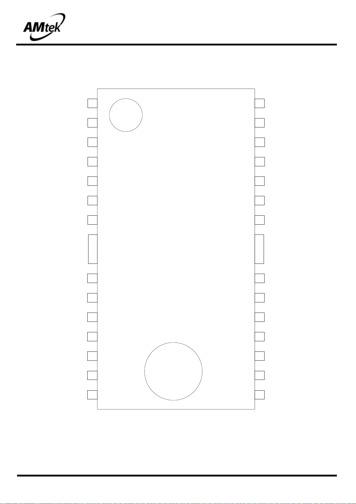
AM5888S
harman/kardon
HS 2X0/230 Service Manual
Page 22 of 73
Pin configuration
VINFC
TRB_1
REGO 2
VINSL+
REGO 1
FWD
Motor Driver ICs
1
2
3
4
5
6
AM5888S
28
MUTE
27
BIAS
26
VINTK
25
TRB_2
24
NC
23
VINLD
REV
Vcc1
VOTR-
VOTR+
VOSL+
VOSL-
VOFC-
22
21
20
19
18
17
16
GND
VCTL
NC
Vcc2
VOLD-
VOLD+
VOTK-
7
8
9
10
11
12
13
k
AAMMtteek
SSEEMMIICCOONNDDUUCCTTOORRS
VOFC+
14
15
VOTK+
S
- 4 -
OOcctt 22000055 VV11..33
Page 23

AM5888S
harman/kardon
HS 2X0/230 Service Manual
Page 23 of 73
Pin description
PIN No Pin Name Function
1 VINFC Input for focus driver
2 TRB_1 Connect to external transistor base
3 REGO2 Regulator voltage output, connect to external transistor collector
4 VINSL+ Input for the sled driver
5 REGO1 Regulator voltage output, connect to external transistor collector
6 FWD Tray driver forward input
7 REV Tray driver reverse input
8 Vcc1 Vcc for pre-drive block and power block of sled and tray
9 VOTR- Tray driver output (-)
Motor Driver ICs
10 VOTR+ Tray driver output (+)
11 VOSL+ Sled driver output (+)
12 VOSL- Sled driver output (-)
13 VOFC- Focus driver output (-)
14 VOFC+ Focus driver output (+)
15 VOTK+ Tracking driver output (+)
16 VOTK- Tracking driver output (-)
17 VOLD+ Spindle driver output (+)
18 VOLD- Spindle driver output (-)
19 Vcc2 Vcc for power block of spindle, tracking and focus
20 NC No Connection
21 VCTL Speed control input of tray driver
22 GND Ground
23 VINLD Input for spindle driver
24 NC No Connection
25 TRB_2 Connect to external transistor base
26 VINTK Input for tracking driver
27 BIAS Input for reference voltage
28 MUTE Input for mute control
Notes) Symbol of + and – (output of drivers) means polarity to input pin.
(For example, if voltage of pin1 is high, pin14 is high.)
k
AAMMtteek
SSEEMMIICCOONNDDUUCCTTOORRS
S
- 5 -
OOcctt 22000055 VV11..33
Page 24

SiI 9034 HDMI Transmitter
harman/kardon
HS 2X0/230 Service Manual
Page 24 of 73
Data Sheet
SiI 9034 HDMI Transmitter Pin Diagram
TX2-
TX2+
AGND
PVCC2
AGND
AVCC33
DDCPWR5V
DSDA
CSCL
DSCL
CI2CA
CSDA
TX1+
AVCC18
TX1-
Silicon Image, Inc.
EXT_SWG
PVCC1
AGND
TXC-
TXC+
AVCC18
TX0-
TX0+
AGND
AGND
4948474645444342414039383736353433323130292827
50
HPD
TMODE
IOVCC33
GND
VPP18
D23
D22
D21
D20
D19
D18
D17
D16
CVCC18
GND
IOVCC33
GND
GND
GND
GND
D15
D14
D13
Silicon Image
D12
D11
51
52
53
54
55
56
57
58
59
60
61
62
63
64
65
66
67
68
69
70
71
72
73
74
75
Sil 9034
100-Pin TQFP
(Top View)
26
25
24
23
22
21
20
19
18
17
16
15
14
13
12
11
10
9
8
7
6
5
4
3
2
1
RESET#
INT
DL3
DR3
DL2
DR2
DL1
DR1
DL0
DR0
DCLK
IOVCC33
GND
CVCC18
SCK
WS
SD0
SD1
SD2
SD3
MCLK
SPDIF
VSYNC
HSYNC
DE
Confidential
SiI-DS-0186-C 2 © 2007 Silicon Image, Inc. CONFIDENTIAL
77787980818283
D8
for
CREATOR CORPORATION
D9
D10
CVCC18 76
GND
GND
8485868788
D7
GND
GND
D6
D5
GND
89
IDCK
IOVCC33
92
91
90
D3D4D1D2D0
93
94
95
GND
96
GND
97
GND
98
GND
100
99
GND
CVCC18
Figure 1. 100-Pin TQFP Pinout Diagram
CHINA
Internal Use Only
Page 25

±15kV ESD Protected MII/RMII 10/100 Ethernet Transceiver with HP Au to-MDIX and flexPWRTM Technology in a Small Footprint
harman/kardon
HS 2X0/230 Service Manual
Page 25 of 73
Chapter 2 Pin Configuration
2.1 Package Pin-out Di agram and Signal T able
TXN
VDDA3.3
30
TXP
29
28
27
nINT/TX_ER/TXD4
COL/RMII/CRS_DV
36
1
VDDA3.3
35
EXRES1
34
VDDA3.3
33
RXP
32
RXN
31
Datasheet
TXD3
MDC
CRS/PHYAD4
MDIO
nRST
TX_EN
VDD33
VDD_CORE
SPEED100/PHYAD0 9RX_DV
2
3
4
5
6
7
8
LAN8700/LAN8700I
MII/RMII Ethernet PHY
36 Pin QFN
GND FLAG
10
11
12
13
XTAL2
LINK/PHYAD1
ACTIVITY/PHYAD2
FDUPLEX/PHYAD3
14
CLKIN/XTAL1
15
RXD3/nINTSEL
16
RXD2/MODE2
17
RXD1/MODE1
18
RXD0/MODE0
26
TXD2
VDDIO
25
24
TXD1
23
TXD0
TX_CLK
22
RX_ER/RXD4
21
RX_CLK/REGOFF
20
19
Figure 2.1 Package Pinout (Top V iew)
Revision 1.5 (10-05-07) 10 SMSC LAN8700/LAN8700i
DATASHEET
Page 26

USB 2.0 High-Speed 4-Port Hub Controller
harman/kardon
HS 2X0/230 Service Manual
Page 26 of 73
Datasheet
LED_A1_N/PRT_SWP1
PRTPWR_POL
SUSP_IND/LOCAL_PWR/NON_REM0
SEL48
VDDA33
USBUP_DM
USBUP_DP
XTAL2
XTAL1/CLKIN
VDD18PLL
RBIAS
VDD33PLL
37
38
39
40
41
42
43
44
45
46
47
48
LED_B1_N/BOOST034VBUS_DET33RESET_N
35
36
HS_IND/CFG_SEL131SCL/SMBCLK/CFG_SEL030VDD3329SDA/SMBDATA/NON_REM128OCS4_N
CFG_SEL2
32
SMSC
USB2514
(Top V iew QFN-48)
Thermal Slug
(must be connected to VSS)
1
2
3
4
5
VDDA33
PRTPWR426OCS3_N25LED_A2_N/PRT_SWP2
27
24
23
22
21
20
19
18
17
16
15
14
13
6
7
8
9
10
11
12
VDDA33
REG_EN
LED_B4_N
LED_B2_N/BOOST1
LED_A3_N/PRT_SWP3
LED_B3_N/GANG_EN
PRTPWR3
OCS2_N
PRTPWR2
VDD33CR
VDD18
OCS1_N
PRTPWR1
TEST
LED_A4_N/PRT_SWP4
SMSC USB2514 7 Revision 1.98 (11-19-07)
USBDN1_DP/PRT_DIS_P1
USBDN1_DM/PRT_DIS_M1
USBDN2_DM/PRT_DIS_M2
USBDN2_DP/PRT_DIS_P2
USBDN3_DM/PRT_DIS_M3
USBDN3_DP/PRT_DIS_P3
USBDN4_DP/PRT_DIS_P4
USBDN4_DM/PRT_DIS_M4
Indicates pins on the bottom of the device.
Figure 1.2 USB2514 48-Pin QFN
DATASHEET
Page 27

K4S643232H
harman/kardon
HS 2X0/230 Service Manual
Page 27 of 73
PIN CONFIGURATION (Top view)
VDD
1
DQ0
VDDQ
DQ1
DQ2
VSSQ
DQ3
DQ4
VDDQ
DQ5
DQ6
VSSQ
DQ7
DQM0
CAS
RAS
A10/AP
DQM2
DQ16
V
DQ17
DQ18
V
DQ19
DQ20
V
DQ21
DQ22
V
DQ23
N.C
VDD
WE
CS
N.C
BA0
BA1
A0
A1
A2
DD
V
N.C
SSQ
DDQ
SSQ
DDQ
DD
V
2
3
4
5
6
7
8
9
10
11
12
13
14
15
16
17
18
19
20
21
22
23
24
25
26
27
28
29
30
31
32
33
34
35
36
37
38
39
40
41
42
43
86
85
84
83
82
81
80
79
78
77
76
75
74
73
72
71
70
69
68
67
66
65
64
63
62
61
60
59
58
57
56
55
54
53
52
51
50
49
48
47
46
45
44
VSS
DQ15
VSSQ
DQ14
DQ13
VDDQ
DQ12
DQ11
VSSQ
DQ10
DQ9
VDDQ
DQ8
N.C
VSS
DQM1
N.C
N.C
CLK
CKE
A9
A8
A7
A6
A5
A4
A3
DQM3
SS
V
N.C
DQ31
DDQ
V
DQ30
DQ29
SSQ
V
DQ28
DQ27
DDQ
V
DQ26
DQ25
SSQ
V
DQ24
SS
V
SDRAM
86Pin TSOP (II)
(400mil x 875mil)
(0.5 mm Pin pitch)
- 6 -
Rev. 1.2 April 2006
Page 28

4. PIN CONFIGURATION
harman/kardon
HS 2X0/230 Service Manual
Page 28 of 73
W9812G6GH
V
DQ0
VCCQ
DQ1
DQ2
V
SS
DQ3
DQ4
V
CC
DQ5
DQ6
V
SS
DQ7
V
LDQM
WE
CAS
RAS
CS
BS0
BS1
A10/AP
A0
A1
A2
A3
V
CC
Q
Q
Q
CC
CC
1
2
3
4
5
6
7
8
9
10
11
12
13
14
15
16
17
18
19
20
21
22
23
24
25
26
27
54
53
52
51
50
49
48
47
46
45
44
43
42
41
40
39
38
37
36
35
34
33
32
31
30
29
28
V
SS
DQ15
VSSQ
DQ14
DQ13
V
Q
CC
DQ12
DQ11
V
Q
SS
DQ10
DQ9
V
Q
CC
DQ8
V
SS
NC
UDQM
CLK
CKE
NC
A11
A9
A8
A7
A6
A5
A4
V
SS
- 4 - Revision A06
Publication Release Date:Aug. 13, 2007
Page 29

W25X16, W25X32, W25X64
harman/kardon
HS 2X0/230 Service Manual
Page 29 of 73
5. PIN CONFIGURATION PDIP 300-MIL
Figure 1c. W25X16, W25X32, W25X64 Pin Assignments, 8-pin PDIP (Package Code DA)
6. PIN DESCRIPTION SOIC 208-MIL, PDIP 300-MIL, AND WSON 6X5-MM
PAD NO. PAD NAME I/O FUNCTION
1 /CS I Chip Select Input
2 DO O Data Output
3 /WP I Write Protect Input
4 GND Ground
5 DIO I/O Data Input / Output
6 CLK I Serial Clock Input
7 /HOLD I Hold Input
8 VCC Power Supply
- 6 -
Page 30

W25X10, W25X20, W25X40, W25X80
harman/kardon
HS 2X0/230 Service Manual
Page 30 of 73
3. PIN CONFIGURATION SOIC 150-MIL
Figure 1a. W25X10, W25X20 and W25X40 Pin Assignments, 8-pin SOIC (Package Code SN)
4. PIN CONFIGURATION SOIC 208-MIL
Figure 1b。W25X40 and W25X80 Pin Assignments, 8-pin SOIC (Package Code SS)
5. PIN CONFIGURATION PDIP 300-MIL
Figure 1c。W25X10, W25X20, W25X40 and W25X80 Pin Assignments, 8-pin PDIP (Package Code DA)
Publication Release Date: September 22, 2006
- 5 - Preliminary - Revision I
Page 31

SAMSUNG
harman/kardon
HS 2X0/230 Service Manual
Page 31 of 73
z 芯片管脚图
14 脚 SOP
MK-900 手册(内部资料)
MK-900 硬件手册
z 芯片管脚说明
管脚号
MK-900
1 P1.0/ADC1 I/O TTL SMT 双向输入输出端口,ADC 模拟信号输入
2 P1.2 I TTL SMT 单向输入端口
3 VSS P
4 /CS I TTL SMT 单向输入端口
5 DAT I/O TTL SMT 双向输入输出端口,数据通信端口
6 CLK I TTL SMT 单向输入端口,时钟通信端口
7 VSS P
8 Vdd P
9 P0.0 I/O
10 P0.1 I/O TTL SMT 双向输入输出端口
11 Vdd P
12 P0.2 I/O TTL SMT 双向输入输出端口
13 P0.3 I/O TTL SMT 双向输入输出端口
14 P1.1/ADC2 I/O TTL SMT 双向输入输出端口,ADC 模拟信号输入
管脚名
I/O
缓冲器
类型
-
-
-
-
-
管脚说明
地,0V 参考点
地,0V 参考点。
电源
电源
z DC 特性参数
最大标称值(Vss = 0V)
第 1 页 共 3 页
Page 32

Logic Diagram
harman/kardon
HS 2X0/230 Service Manual
Page 32 of 73
FSAV330
Connection Diagram
Pin Descriptions
Pin Name Description
OE
S Select Input
ABus A
B
1–B2
Bus Switch Enable
Bus B
Truth Table
SOE Function
X H Disconnect
LL A
HL A
B
1
B
2
www.fairchildsemi.com 2
Page 33

Si4704/05
harman/kardon
HS 2X0/230 Service Manual
Page 33 of 73
6. Pin Descriptions: Si4704/05-GM
NC
1
NC
FMI
2
GPO1
GPO2/INT
GPO3/DCLK
17181920
16
15
DFS
DOUT
RFGND
LPI
3
4
GND
PAD
5
6
7 8 9
SEN
Pin Number(s) Name Description
1, 20 NC No connect. Leave floating.
2 FMI FM RF input.
3 RFGND RF ground. Connect to ground plane on PCB.
4 LPI Loop antenna RF input.
5 RST Device reset (active low) input.
6 SEN Serial enable input (active low).
7 SCLK Serial clock input.
8 SDIO Serial data input/output.
9 RCLK External reference or crystal oscillator input.
10 VIO I/O supply voltage.
11 VDD Supply voltage. May be connected directly to battery.
13 ROUT Right audio analog line output.
14 LOUT Left audio analog line output.
15 DOUT Digital audio output data.
16 DFS Digital frame synchronization.
17 GPO3/DCLK General purpose output/digital bit synchronous clock or crystal oscillator
input.
18
19 GPO1 General purpose output.
12, GND PAD GND Ground. Connect to ground plane on PCB.
GPO2/INT
General purpose output/interrupt.
SCLK
SDIO
10
VIO
RCLK
14
13
12
11
LOUT
ROUT
GNDRST
VDD
28 Preliminary Rev. 0.8
Page 34

PRELIMINARY DATA SHEET MSP-M/MAP-M
54113
114
115
116
117
118
119
120
121
122
123
124
125
126
127
128
53
52
51
50
49
48
47
46
45
44
43
42
41
40
39
123456789101112131415161718192021222324
102101100999897969594939291908988878685848382818079
25 26 27 28 29 30 31 32
78 77 76 75 74 73 72 71
55
56
57
58
59
60
61
62
63
64
103
104
105
106
107
108
109
110
111
112
70 69 68 67 66 65
33 34 35 36 37 38
I2S_OUT1_WS
I2S_OUT1_CL
VDD_CORE
VDD_CORE
VSS_CORE
VSS_CORE
VSS_IO
VDD_IO
I2S_OUT2_CL
I2S_OUT2_WS
I2S_OUT2_D
SPDIF_OUT3
SPDIF_OUT2
SPDIF_OUT1
SPDIF_OUT4
PWM_2M
PWM_1P
PWM_1M
MAIN_OUT6
MAIN_OUT5
SGND_AU
VREF_AU
MIC_INL/LINE_IN8L
MIC_INR/LINE_IN8R
VSS_AU
VDD_AU
LINE_OUT3R
LINE_OUT3L
LINE_OUT2R
LINE_OUT2L
LINE_OUT1R
SPDIF_IN1
SPDIF_INREF
SPDIF_IN2
SPDIF_IN4
VDD_SPDIF
VSS_SPDIF
VSS_CORE
VSS_CORE
VDD_CORE
SPDIF_IN3
VDD_CORE
I2S_DEL_OUT
I2S_DEL_IN
I2S_DEL_WS
I2S_DEL_CL
SPI_CL
LINE_IN2R
LINE_IN3L
LINE_IN3R
LINE_IN4L
LINE_IN4R
LINE_IN5L
LINE_IN5R
LINE_IN6L
LINE_IN6R
LINE_IN7L
LINE_IN7R
LINE_OUT1L
LINE_IN2L
LINE_IN1R
LINE_IN1L
NC
PWM_2P
PWM_3M
PWM_3P
VDD_PWM
VSS_PWM
PWM_4M
PWM_4P
TEST
XT1
XT2I2S_IN1_D2
I2S_IN1_D3
I2S_IN1_D4
I2S_IN3_CL
I2S_IN3_WS
I2S_IN3_D
I2S_OUT1_D4
I2S_OUT1_D3
I2S_OUT1_D2
I2S_OUT1_D1
I2S_IN1_WS
I2S_IN1_CL
VDD_IO
VSS_IO
SPDIF_OUT5
VSS_CORE
VSS_CORE
VDD_CORE
VDD_CORE
I2S_IN1_D1
I2S_IN2_CL
I2S_IN2_WS
I2S_IN2_D
CLKO
GPIO0
GPIO1
VALID_1
SHUTDOWNQ
RESETQ
NC
NC
NC
VDD_XTAL
VSS_XTAL
NC
NC
NC
NC
V
ALID_2
VALID_3
VA
LID_4
VDD_DIG
VSS_DIG
SDA
SCL
VDD_PLL
VSS_PLL
ADR_SEL
NC
VSS_IO
VDD_IO
SPI_CS
SPI_DIN
SPI_DOUT
MAP 5601M
harman/kardon
HS 2X0/230 Service Manual
Page 34 of 73
Fig. 4–6: MAP 5601M in PMQFP 128 -2 package
Micronas April 23, 2008; PD000200_001EN 137
Page 35

www.ti.com
1
2
3
4
5
6
7
8
9
10
11
12
13
14
15
16
17
18
19
20
21
22
GVDD_B
OTW
NC
NC
SD
PWM_A
RESET_AB
PWM_B
OC_ADJ
GND
AGND
VREG
M3
M2
M1
PWM_C
RESET_CD
PWM_D
NC
NC
VDD
GVDD_C
DDV PACKAGE
(TOP VIEW)
GVDD_A
BST_A
NC
PVDD_A
PVDD_A
OUT_A
GND_A
GND_B
OUT_B
PVDD_B
BST_B
BST_C
PVDD_C
OUT_C
GND_C
GND_D
OUT_D
PVDD_D
PVDD_D
NC
BST_D
GVDD_D
44
43
42
41
40
39
38
37
36
35
34
33
32
31
30
29
28
27
26
25
24
23
P0016-02
TAS5352
harman/kardon
HS 2X0/230 Service Manual
Page 35 of 73
SLES204A–SEPTEMBER2007–REVISEDOCTOBER2007
Thesedeviceshavelimitedbuilt-inESDprotection.Theleadsshouldbeshortedtogetherorthedeviceplacedinconductivefoam
duringstorageorhandlingtopreventelectrostaticdamagetotheMOSgates.
GENERALINFORMATION
TerminalAssignment
TheTAS5352isavailableinathermallyenhanced44-pinHTSSOPPowerPad™package(DDV)
Thispackagecontainsathermalpadthatislocatedonthetopsideofthedeviceforconvenientthermalcoupling
totheheatsink.
2SubmitDocumentationFeedbackCopyright©2007,TexasInstrumentsIncorporated
ProductFolderLink(s):TAS5352
Page 36

harman/kardon
HS 2X0/230 Service Manual
Page 36 of 73
Page 37

harman/kardon
HS 2X0/230 Service Manual
Page 37 of 73
Page 38

harman/kardon
HS 2X0/230 Service Manual
Page 38 of 73
Page 39

harman/kardon
HS 2X0/230 Service Manual
Page 39 of 73
Page 40

harman/kardon
HS 2X0/230 Service Manual
Page 40 of 73
Page 41

harman/kardon
HS 2X0/230 Service Manual
Page 41 of 73
Page 42

harman/kardon
HS 2X0/230 Service Manual
Page 42 of 73
Page 43

harman/kardon
HS 2X0/230 Service Manual
Page 43 of 73
Page 44

harman/kardon
HS 2X0/230 Service Manual
Page 44 of 73
Page 45

harman/kardon
HS 2X0/230 Service Manual
Page 45 of 73
Page 46

harman/kardon
HS 2X0/230 Service Manual
Page 46 of 73
Page 47

harman/kardon
HS 2X0/230 Service Manual
Page 47 of 73
Page 48

harman/kardon
HS 2X0/230 Service Manual
Page 48 of 73
Page 49

harman/kardon
HS 2X0/230 Service Manual
Page 49 of 73
Page 50

harman/kardon
HS 2X0/230 Service Manual
Page 50 of 73
Page 51

harman/kardon
HS 2X0/230 Service Manual
Page 51 of 73
Page 52

5
harman/kardon
HS 2X0/230 Service Manual
Page 52 of 73
4
3
2
1
HS2X0 BLOCK DIAGRAM
HDMI Block
SiI9034
HDMI output
Not for HS2X0
D D
SDRAM
4*2M*16b
SPI
Flash
16Mb
NAND
FLASH
1Gb
SDRAM
4*4M*16b
SDRAM
4*512K*32b
M1
Switch
FST3257
USB WIFI Moduler
AR2524+UW2453
USB HUB
USB2514
Ethernet Transceiver
LAN8700C
WIFI Antenna
Front USB
Rear USB
Ethernet
CVBS output
Vedio Driver
HDMI upscaler
FMS6143
FLI2310-LF-CF
C C
Motor Driver
Servo Decoder
MPEG
TAMUL
TMD8809X02
Buffer
74LVC244
CCIR656
MPEG
Amlogic
AML8218
Tuner Silicon Lab
Si4705
AM5888S
Audio
Processor
S-Video output
Scart out/in
(EU version only)
FM Antenna
Scart audio input
Line in2
Line in1
Line out
Multak
MCU
MK-908
B B
MAP5601M-E5-900
Headphone
Coaxial output
Coaxial In1
Optical In1
Coaxial In2
Optical In2
Subwoofer line outpu t
2 channels output
Sub Trigger output
Slot in
Loader
Hitachi
HOP-1200W
VFD Driver
LC75711NE
VFD Display
VFD22-1303F
VFD Filament
Power Supply
NCP3063 +
Transformer
EM78P156ELM-G
Functional
buttons
MCU
IR
receiver
Standby control
Power
indicator
SMPS Board
Supply power
for all boards
SPI
Flash
8Mb
Amplifier output
TAS5352
Sub trigger control
Front Panel Board
A A
FST3257MTC
AC Power cord
Title
HS2X0 DIAGRAM 100329
Size Document Number Rev
A3
Date: Sheet
BLOCK DIAGRAM 1.5
121Monday, March 29, 2010
1
of
5
IR In/Out Block
4
3
IR out
2
IR in
Page 53

5
harman/kardon
HS 2X0/230 Service Manual
Page 53 of 73
4
3
2
1
TI AMPLIFIER
PART
(2CH*65W)
COAX
IN1
COAX
IN2
WHITE
BLACK BLACK RED
<6>:BANDING POST
BOARD (3523C)
2
CN501
AC Input
USB
Front
HP
Title
HS2X0 Wiring DIAGRAM_20090304
Size Document Number Rev
A2
Wiring Diagram
Date: Sheet
1
AC Power cord
~100-240V
Same as HS200
1
20 20Monday, March 29, 2010
1.2
of
LINE2
LINE1
INR
LINE2
INL
C
INR
LINE1
INL
CN401
GND
1
HP_L
2
DGND
3
4
HP_R
5
FPMCU_MUTE
DGND6
I2S_MCLK
7
8
DGND
I2S_ACL
9
I2S_AWS
10
DGND
11
12
I2S_HDMI_D
13
DGND
14
SPDIF_MAP_HDMI
DGND
15
16
SPDIF_AML
17
DGND
18
NC
NC
19
DGND
20
I2S3_AML
21
DGND
22
2324AMP_TWAN
DGND
<2>:AV BOARD (5983C)
NOTE (MAP GPIO): TVFORMAT1,
TVFORMAT0,YC_CVBS_SWITCH...
1.0mm flat
cable (9P)
CN504
A+5V
DGND
VOL+
VOL-
LED_CONTROL
DGND
WiFi
Antenna
<7>: WIFI BOARD(3874C)
<1>: MAIN BOARD(5982C)
4
CN5CN403
CN10
CN9
14
13
12
11
10
9
8
7
6
5
4
3
2
1
20
18
17
16
15
14
13
12
11
10
9
8
7
6
5
4
3
2
1
1
2
3
4
5
6
7
8
9
10
11
12
13
14
15
16
17
18
19
20
21
22
23
24
1
2
3
4
5
6
7
8
9
10
11
12
S-VIDEO
OUT
DGND
NC
DGND
5VON
DGND
SCART_CVBS
DGND
SCART_C_OUT
DGND
NC
DGND
SCART_Y_OUT
DGND
NC
DGND
I2C_DATA_AV19
DGND
I2C_CLK_AV
DGND
DGND
I2S_DVD_WS
I2S_DVD_CL
DGND
I2S_0_DVD
I2S_1_DVD
DGND
I2S_2_DVD
NC
DGND
SPDIF_INTO_DVD
DGND
SPDIF_DVD
DGND
DGND
DVD PART
GND-LD
LD-DVD
NC
HFM
MD
CD-LD
DVD_VR
CD_VR
NC
E
S5V
VC_OPU
GND-PD
F
B
A
DVDRFP
CD_DVD
D
C
TRACKTRACK+
FOCUS+
FOCUS-
SW4
SW1
SW2
SW3
SPINSPIN+
LOADLOAD+
GND
SW5
SLEDSLED+
CVBS
OUT
VFD 12COLUMNS × 1LINE 5×7 DOT MATRIX
FM
Antenna
D D
C C
B B
Foryou DL-05MH
Slot-in LOADER
Hitachi HOP-1200W
A A
HS2X0 CNT REF NO. ASSIG NM ENT
SMPS 6144C: from 500-599
Front panel board 6184C/6185C: from 600-699
Main board 5982C: from 1-399
AV board 5983C: from 400-499(4R..)
SCART
1
2
3
4
5
1.0mm flat
6
cable
7
8
(14P)
9
10
11
12
D
13
14
CN404 CN6
1
2
3
4
5
6
7
8
9
1.0mm flat
10
cable
11
12
(20P)
13
14
15
16
F
17
18
19
20
Same as HS200
0.5mm flat
cable (24P)
1.0mm flat
cable (12P)
12 pins 24 pins
Same as HS200
5
OUT
VFD_STB
MCU_OFF
I2C_DATA_VFD_FLI
I2C_CLK_VFD_FLI
3251210
1
CN4
1.0mm flat
cable (14P)
CN601
REMOTE
CONTROL
(FROM IR IN/OUT JACK)
DGND
DGND
IR
FRONT_LED
IR_IN
7
9
6134
8
A
Same as HS200
14 pins
USB
DGND
NC
NC
HP_DETECT
14
11
HDMI OUT
1.0mm flat
cable (8P)
MAIN
POWER
(FPMCU_MUTE)
MCU_MUTE
HP_L
DGND
DGND
DGND
FP_DP
FP_DM
4861523
7
CN2
BH
Same as HS200
8 pins
CN603
IN
DGND
<4>: FRONT PANEL BOARD (6184C/6185C)
3
HP_R
Ethernet
DGND
S+5V
DGND
+12V
DGND98
USB5V
DGND
USB5V
DGND
5.7V
5.7V
A+5V
CN3
CN1
12
11
10
7
6
5
4
3
2
1
24
23
22
21
20
19
18
17
16
15
14
13
12
11
10
9
8
7
6
5
4
3
2
1
1.0mm flat
cable (22P)
E
1.25mm flat
cable (12P)
COAX
AUDIO
OUT
OUT R
AUDIO
OUT L
3.3V
-12V
5V0N
+12V
DGND
12VON
54613
2
CN405
KL
Same as HS200 Same as HS200
9 pins
CN505
SUB
A5V
DGND
7
8
DGND
9
SUB
TRIGGER
+34V
1
CN400
Amplifier Power
Supply
CN506
<5>: SMPS(6144C)
12 pins
DGND
DGND
DGND
DGND
USB5V
+5VON12USB5V
-12V
A+5V
+12V
14 pins
CN605
6 pins
STANDBY
10
11
2
1456789
CN503
1.25mm flat
cable (14P)
CN602
CN604
1
2
3
4
5
6
+3.3V
2
3
J
DGND
13
OPTICAL
IN2 IN1
PGND
2
NC
14
Page 54

5
harman/kardon
HS 2X0/230 Service Manual
Page 54 of 73
4
3
2
1
NO.
REVISION DATE
REV
1. R3 -> ON, R7 on->off, R8 off->on
2. U11 -> OFF, U10 -> ON
3. R71 R72 R78 R79 -> ON
D D
4. U21 Pin9 GND -> VCC and add R31=4.7K
5. Change R162 from 4.7K to 0R
6. Crrect spindle signals by swap them.
7. Add pull-up resistors onto I2C
8. Change to high speed logic device SN74LVC2G04DCKR for 50MHz crystal.
1
July 8, 2008
Hitachi version
EV1
1.0
9. Delete YUV output, reassign the output AML_CVBS, AML_Y and AML_C.
10. Delete analog conversion chip TVP7000, add FLI2310 to convey the signal between
AML8218 and SiI9034, add reset signal of U6.158
11. Delete SDRAM2 of U6, and change the SDRAM1to 256M capability, reassign the HDMI
output of AML8218.
12. Delete the SDIO interface for WiFi, replace it with USB Hub and USB interface WiFi.
13. Delete U11, not useful.
14. Reassign the IEC958 output from U6.135 to
U6.141.
15. Delete HYNC. VSYNC, FID signals of 5029, and pin77 78 81 leave float.
16. Repalce SN74ALVCH16827-DGG with SN74ALVC244PW, and
C C
move to AML8218 page
,
delete Video buffer page
1. Pin13,17,19 of USB2514 must be connected to GND
2. Change C68, C70 to 20p
3. R91 -> 1.5K, R140 -> 1.2K
4. R50 -> N/A
5. Move R7 value to R6, NOR FLASH
2
Dec 18, 2008
EV2
1.1
6. C237 -> R262 = 22R
7. Correct USB data signal and WIFI PORT1, PORT2
8. Change the power supply of U8 to 3.3V
9. In debug mode, R42 shoud be N/A
10. Change SDRAM to Samsung brand, modify the data signals between SDRAM and flash.
11. Add WIFI antenna connection
12. Change the data signal of SDRAM.
B B
1. Add pull-up R71 to HP_DETECT
2. Replace the intergrated network connector with discrete connector.
3. Separate the analog power supply for FLI2310
3
Mar 10, 2009
EV3
DV1
4. Modify the burning signal of servo flash U18, add switch FST3257.
1.2
5. Modify the reset signal for samsung chip to AML8218.
6. Delete R181, C137
7. Delete crystal of FLI2310, nor flash of AML8218, EEPROM of S5L5029
8. Delete optional capacitor for clock between s5l5029 and AML8218, choose resistor to connect.
9. Add 12MHz crystal for AML8218
Aug 15, 2009
4
DV2
Dec 12, 2009
5
6
PV
Jan 22, 2010
MP 1.5 1. R229, R250, R254 -> 68R
A A
1. Modify 50MHz crytal to 50MHz active crytal.
2. Enlarge the capacitor to 1000uF for USB5V power supply, improve HDD noise plugging in.
1.3
3. Add PTC3.
1. RFSUM C97(102) -> 681
1.4
2. RFEQO C120(561) -> 681
3. FOD R175(2.2k) -> 47k, R165(30k) -> 0, C128(222) ->151
4.TRD R176(2.2k) ->47k, R164(43k) -> 0, C129(222) ->151
5. SLD R163(20k) ->15k
6. DVD VR: R150 - 100 ohm – pin78 P4.3
REVISION HISTORY
17. SPI modification:
(1) Change I2C_DATAS from p1.0 to p5.3, delete the connection between p5.3
and SPI_FAIL_, SPI_FAIL connect 1K ohm and then to GND.
(2) Change SPI_CONTROL_CLK_ from p1.2 to p1.0, leave p1.2 vacant.
(3) Change P1.5 from sip_sop to spi_ack
(4) Delete the connection between buffer 1Y2, 1Y3 and RN43.2, RN43.3;
connect RN43.2, RN43.3 to GND.
NANDFLASH modification
(1) R8 -> OFF, R7 -> ON
(2) Pull 4.7Kohm from R73 to U11.8, left of R85 connect to NAND_VCC3
18. Change net name of PIN32 33 on AML8218, from VSYNC,
HSYNC to SPI_FAIL, SPI_SOP, and pull down 1Kohm resistor to
GND, delete SPI_FAIL and SPI_SOP of 5029
19. AML8218 and S5L5029 share 27MHz clock.
20. Move MCU_OFF from pin212 to pin 108, pin212 change to I2S3_AMCLK, I2S3_AMCLK
and I2S_HDMI_MCLK connect to I2S_MCLK then to CN1.18, I2S_AML_CL and
I2S_HDMI_CL connect to I2S_ACL then to CN1.16, I2S_AML_WS and I2S_HDMI_WS
connect to I2S_AWS then to CN1.15, delete CN1.7 and CN1.6 net I2S_AML_WS and
I2S_AML_CL
21. Delete the crystal of AML8218 on USB port.
22. Delete CE13
23. Divide the 27M clock into 13.5M for FL2310 and add D-trigger.
13. Add R266 and R268 onto I2C of HDMI
14. Move I2C of VFD from GPIOC_2,3 to GPIOC_19,18; I2C of HDMI from GPIOC_19,18 to
GPIOC_2,3; FLI2310 share I2C with VFD
15. Add pull-up resistor onto DATA, CLK of I2C
16. SPI DMA modification
RN40 pin 6 connect 15p to GND
RN40 pin 2 connect 3.3k resistor to 3.3V
RN40 pin 3 connect 3.3k resistor to 3.3V
17. R59 -> 0R
18. Add a resistor 1K between pin8 and vcc of MK900.
19. Add pull-up resistor to CS of MK900
20. ADD DC/DC convertor, reassign power for chips.
21. Modify the connector between mainboard and SMPS board
10. Modify the core power supply for AML8218 with DC/DC.
11. Enhance the core power supply of AML8218.
12. Modify the video output capacitors and resistors, add clamp diodes on them,
to improve the performance.
13. Change R252 to 82R
14. Change C119 and C127 to 20pF.
15. Add optional clock net for AML8218.
16. R5 -> OFF, R6 -> ON
17. rn1 -> N/A
4. Change R58 to 100R, to improve the wave of SPDIF input.
5. Change R179 R180 to 100R, to improve CD player noise.
6. Change C15 from Y5V to X7R, to improve the video performance stability.
:
:
7. CD VR: R151 - 100 ohm – pin81 P6.2
5
Title
HS2X0 MAIN BOARD - 100309
Size Document Number Rev
5982Y 1.0
A3
4
3
2
Date: Sheet
11Tuesday, March 09, 2010
1
of
Page 55

5
harman/kardon
HS 2X0/230 Service Manual
Page 55 of 73
4
3
2
1
NO.
D D
REVISION DATE
1
June 05, 2008
TI version
EV1
REV
1. Add 25V note to C491 and C492.
1.0
2. Delete AM tuner circuit.
3. Modify SCART output from RGB to YC.
4. Add E5 version to MAP4601.
5. R459, R460 -> ON
REVISION HISTORY
7. R415 -> 1.6K, adjust volage to 1.01V
8. 4R48 -> 47K, 7A for current limited.
9. Reset SPDIF_IN parameters.
10. Delete AMP_TWARN connection on MAP4601, connect this net to mainboard
11. Add pull-up resistor to net VALID.
6. Delete net I2S_3_DVD
1. In order to synchro clock, TUNER, ALM8218, HDMI, MAP commonly use same AMCLK, BCK and WS.
2. Delete nets I2S_AML_CL, I2S_AML_WS, change I2S_HDMI_MCLK to I2S_MCLK, change
2
Jul 22, 2008
EV1
1.1
I2S_HDMI_CL to I2S_ACL, change I2S_HDMI_WS to I2S_AWS
3. Invert the input signals twice in the 74HC158.
4. Correct the BAV99 package.
6. Add CE406 CE407 to improve THD+N performance.
5. Change the optical-coaxial combined terminal to discrete components.
3
Dec 23, 2008
EV2
C C
4
Mar 09, 2009
DV1
1. 4R31, 4R32 -> 22R
1.2
2. Connect pin106, pin107, pin90, pin91 to nets.
3. Add EEPROM for AC3 decode.
1. Comfirm the MAP part number is MAP5601-E5-900 for our use.
1.3
2. R431 -> 750R
、
R436-> 220R, Q409 -> BC847.
3. Modify the crystal circiut for Si4705
4. Change 78l08 to L7808.
5. Swap and correct the net name of optical1 and optical2.
6. Confirm the tuner chip part number is Si4705.
5. Change the PWM2 output to PWM4 in MAP.
6. Add CE408 to improve plop noise in Harman subwoofer during power on.
7. Q406, Q407, Q410 -> ON
4. Correct the phase of AMPLIFIER OUT R+-.
5
Sep 03, 2009
DV2
6
7
Dec 12, 2009
PV
Jan 21, 2009
MP1
1. Replace 74HC158 with FST3257
1.4
2. Coaxial output modification, to meet the spectification of IEC60958.
1.5 1. Only layout changed, to improve CD player noise.
1.6
B B
A A
Title
HS2X0 AV BOARD - 100309
Size Document Number Rev
5983Y 1.0
5
A3
4
3
2
Date: Sheet
11Tuesday, March 09, 2010
1
of
Page 56

5
harman/kardon
HS 2X0/230 Service Manual
Page 56 of 73
CN2
CN1
CON24_1.0MM_DIP_2
24
24
23
23
22
22
21
21
20
20
19
19
18
18
D D
C C
B B
17
17
16
16
15
15
14
14
13
13
12
12
11
11
10
10
9
9
8
8
7
7
6
6
5
5
4
4
3
3
2
2
1
1
E
TO AV BOARD
CN5
CON14_1.0MM_DIP_2
14
14
13
13
12
12
11
11
10
10
9
9
8
8
7
7
6
6
5
5
4
4
3
3
2
2
1
1
D
TO AV BOARD
20
20
19
19
18
18
17
17
16
16
15
15
14
14
13
13
12
12
11
11
10
10
9
9
8
8
7
7
6
6
5
5
4
4
3
3
2
2
1
1
CN6
CON20_1.0MM_DIP_2
F
TO AV BOARD
DGND
I2S_MCLK
I2S_ACL
I2S_AWS
I2S_HDMI_D
COAXIAL_OUT
SPDIF_AML
I2S3_AML
AMP_TWARN
DGND
5VON
SCART_CVBS
SCART_C_OUT
SCART_Y_OUT
DGND
I2C_DATA_AV
I2C_CLK_AV
I2S_DVD_WS
I2S_DVD_CL
I2S_0_DVD
I2S_1_DVD
I2S_2_DVD
SPDIF_INTO_DVD
SPDIF_DVD
HP_L
HP_R
MCU_MUTE
TO AV BOARD
8pin 1.0MM DIP
B
CN4
CON14_1.0MM_DIP_2
A
10
11
12
13
14
TO FP BOARD
SCREW HOLE
VIA1
VIA_PAD4.0
789
DGND
VIA3
VIA_PAD4.0
789
DGND DGND
LOCATION PAD
M1
1
M4
1
HP_R
8
8
7
7
HP_L
6
6
5
5
4
4
3
3
2
2
1
1
1
1
2
2
3
3
4
4
5
5
6
6
7
7
8
8
9
9
10
11
12
13
14
VIA2
1
2
3
4
5
6
1
2
3
4
5
6
VIA_PAD4.0
VIA4
VIA_PAD4.0
M2
1
M5
1
4
MCU_MUTE
FP_DP
FP_DM
MCU_OFF
I2C_CLK_VFD_FLI
I2C_DATA_VFD_FLI
VFD_STB
IR
FRONT_LED
IR_IN
HP_DETECT
789
DGND
789
M3
1
M6
1
POWER INPUT FROM
EXTERNAL POWER
BOARD
CN3
CON12_1.25MM_DIP_2
C
10
11
12
1
2
3
4
5
6
7
8
9
A+5V
1
2
3
4
5
6
7
8
9
10
11
12
5.7V
+12V
S+5V
50R
FB1
FB3
FB4 50R
FB5
50R
50R
3
D+12V
U22
D5.7V
5.7V
D+12V
RF5V
USB5V
MVCC
KA7805
1 3
Vin Vout
GND
2
DGND
Analog Video, HDMI 5V
FB2
FB26 50R
C172
104
DGND
50R
5.7V
2
DDC+5V
VIDEO5V
D10
1N5393 DIP
1 2
5.7V
CE2
100uF/10V
D11
1N5393 DIP
1 2
CE4
100uF/16V
1
4
23
CE3
47uF/10V
4
23
12
+
1.8V_HD
1.8V_FLI
1.8V_HD
C3
103
1.8V_FLI
C8
103
U2
AZ1117H-1.8V
TAB
12
+
C2
104
12
+
C4
104
ADJ
1
U23
AZ1117H-1.8V
ADJ
1
OUTIN
SiI Core 1.8V
TAB
OUTIN
FLI Core 1.8V
DGND
C111
103
D5.7V
12
C89
+
CE7
220uF/10V
1
2
3
4
5
6
1
2
3
4
5
6
A+5V
104
1 2
AML, Samsung Core Power
CE8
220uF/10V
AML,SDRAM,Flash,MCU 3.3V
RMII Ethernet 3.3V
U28
MP1411DH
1
NC1
2
BS
3
NC2
4
IN
5
SW
L19
SPI1048QR-150 15uH/3A
D1
B340LA
12
+
DGND
+3.3V
FB8
C10
104
SS
EN
COMP
FB
GND
GND
C19
104
50R
CE10
100uF/16V
DGNDUSBGND
C237 104
10
9
C239 392
8
7
6
11
U4
AZ1117H-3.3V
ADJ
1
DGND
12
+
DGND
R91 10K
R2 12K
R1 21K
C64
Vout= 0.92*(R1+R2)/R2
22uF/10V Ceramic
4
TAB
23
OUTIN
RMII_3.3V
RMII_3.3V
C11
104
EN=open=automatic startup
FB27 50R
CE13
470uF/10V
12
+
CE9
100uF/10V
DGND
DGND
4
23
4
23
AML_CORE
CE6
47uF/10V
3.3V_HD
+3.3V
12
+
3.3V_HD
+3.3V
C6
103
AML_CORE
5.7V
12
+
CE1
2V5
12
+
DAC_3.3V
C9
104
100uF/10V
CE47
100uF/10V
5.7V
2V5
12
+
C5
104
U1
AZ1117H-3.3V
C1
104
U11
AZ1117H-3.3V
C18
104
U3
AZ1117H-ADJ 1%
TAB
OUTIN
ADJ
1
TAB
OUTIN
ADJ
1
SiI 3.3V
TAB
OUTIN
ADJ
1
FLI, RMII, USB HUB 3.3V
4
23
R285
510R 1%
R286
22R 1%
Vout= 1.25*(Rout+Radj)/Rout+Iadj*Radj
AML_Core = 1.30V 1%
DAC_3.3V
DGND
C12
104
FB7
VCC_SDRAM1
50R
12
DGND
+
CE11
100uF/16V
FB41 50R
FB42 50R
SDRAM 3.3V
VCC_SDRAM1
MCU_VCC3
NAND_VCC3
A A
Title
HS2X0 MAIN BOARD - 090718
5
Size Document Number Rev
A3
Harman/Kardon - 5982Y
4
3
2
Date: Sheet
01 10Monday, March 29, 2010
1
of
1.5
Page 57

5
harman/kardon
HS 2X0/230 Service Manual
Page 57 of 73
4
3
2
1
AVDD_DAC
C14
104
R20 82R 1%
DAC_3.3V
10R
0R N/A
44.2R 1%
USBGND
Y1
12.000MHz-49s-20p N/A
3
C247
20pF N/A
IRVCC
CLK
DATA
/CS
GND
P1.2
P1.0
GND
R62 1K
M1_DQM0
M1_DQM1
M1_CLKO
M1_WE_n
M1_CAS_n
M1_RAS_n
M1_SCS0_n
M1_BA0
M1_BA1
12
CE12
+
10uF/16V
USB5V
I2C_DATA_AV
I2C_CLK_AV
I2C_DATA_VFD_FLI
I2C_CLK_VFD_FLI
I2C_DATA_HDMI
I2C_CLK_HDMI
78
R29 22R
6
R30 22R
5
R35 22R
4
3
2
1
DGND
U29
SN74ALVC244PW
10 11
GND 2A1
9
2Y1
8
1A4
7
2Y2
6
1A3
5
2Y3
4
1A2
3
2Y4
2
1A1
1
1OE
SWITCH SPI AND CCIR656
Title
Size Document Number Rev
A2
Date: Sheet
M1_A6
M1_A4
M1_A9
M1_A7
M1_A8
M1_A5
M1_A_3
M1_A_4
M1_A_5
M1_A_6
M1_A_7
M1_A_8
M1_A_9
PLLC_AVDD33
PLLC_AVSS33
PLLB_AVDD33
PLLA_AVDD33
PLLB_AVSS33
PLLA_AVSS33
125
126
128
127
129
AVDD2
AVDD3
GND
AVDD1
AVDD3
AVDD2
I2C_CLK_VFD_FLI
I2C_DATA_VFD_FLI
FRONT_LED
VFD_STB
M1_A10
M1_A11
M1_A_10
M1_A[0..12]
M1_A12
67
68
M1_A_12
M1_A_11
VDAT0_O
M1_A[0..12]
Memory
M1_SCS0_n
M1_DQM0
M1_RAS_n
M1_WE_n
M1_DQM1
M1_CLKO
M1_CAS_n
777879
5262668184
M1_WE_n
M1_CLKO
M1_DQM0
M1_DQM1
M1_CAS_n
M1_RAS_n
GPIOA_2/FEC_D2
GPIOA_3/FEC_D3
GPIOA_4/FEC_D4
GPIOA_5/FEC_D5
GPIOA_1/FEC_D1
GPIOA_0/FEC_D0
2122232526272831323334
20
19
BTCLK_O
VDAT1
VDAT2
VDAT3
VDAT4
VDAT5
VDAT6
VDAT7
DAC_3.3V Core3.3VCore_AML
3
M1_BA0
M1_BA1
80
M1_BA0
M1_BA1
M1_SCS0_n
GPIOA_6/FEC_D6
GPIOA_7/FEC_D7
GPIOA_8/FEC_CLK
GPIOA_9/FEC_SOP
GPIOA_10/FEC_FAIL
SPI_FAIL
SPI_SOP
R51 1K
R52 1K
SPI_CONTROL_CLK
SPI_D_VAL
SPI_CONTROL_I
SPI_CONTROL_O
FB15 50R
100uF/16V
GND
30
46556373828399
18
DVSS
DVSS
DVSS
DVSS
DVSS
DVSS
GPIOC_0/REMOTE
GPIOC_1/SPDIF_OUT
GPIOA_11/FEC_D_VALID
GPIOA_12
GPIOA_13
134
135
136
35
NAND_nCS2
REMOTE
SPI_D_VAL
R44 4.7K
C39 6.8P N/A
R47 4.7K
R46 100R
Core3.3V
RF5V
SPI_ACK
12
+
CE20
DGND
139
150
168
186
205
DVSS
DVSS
DVSS
DVSS
DVSS
VSS33
P O W E R
GPIOC_2/I2C_M_DATA
GPIOC_3/I2C_M_CLK
GPIOC_4/PWM_A
GPIOC_5/PWM_B
GPIOC_6/ISO7816_RESET
GPIOC_7/ISO7816_DETECT
GPIOC_8/ISO7816_DATA
GPIOC_9/ISO7816_CLK
137
140
141
142
143
144
145
SiI9034_INT
IEC958
HDMI_RESET
BURN_SWITCH
VFD_STB
FRONT_LEDFRONT_LED
TP3
R45 330R
HDMI_RESET
SiI9034_INT
I2C_DATA_HDMI
I2C_CLK_HDMI
C40
C41
104
104
Core3.3V Core_AML
24
415164657687102
VDD33
VDD33
VDD33
VDD33
VDD33
VDD33
VDD33
GPIOC_10
GPIOC_11
GPIOC_12
GPIOC_13
GPIOC_14
GPIOC_15/SD_CLK
GPIOC_16/SD_CMD
GPIOC_17/SD_D0
146
147
148
149
151
152
153
155
MK_CS
RMII_nINT
RMII_nRST
RMII_MODE2
AMP_TWARN
EXT_VBO_N1
TP20
I2C_CLK_AV
I2C_DATA_AV
C42
C43
104
104
Core3.3V
138
154
172
189
208
VDD33
VDD33
VDD33
VDD33
VDD33
GPIOC_18/SD_D1
GPIOC_19/SD_D2
GPIOC_20/SD_D3
156
157
158
FLI_RESET_N
RMII_nINT
FLI_RESET_N
RMII_nRST
C45
C44
104
104
29
133
195
VDD12
VDD33
VDD12
VDD12
VDD12
VDD12
GPIOB_6/RMII_RX_DATA1
GPIOB_3/RMII_RX_CRS_DV
GPIOB_2/RMII_RX_ERR
GPIOB_7/RMII_RX_CLK50
GPIOB_5/RMII_RX_DATA0
GPIOB_1/RMII_TX_DATA1
GPIOB_0/RMII_TX_DATA0
GPIOB_4/RMII_TX_EN
96
929195
97949398100
RMII_CRS_DV
RMII_CLK50
RMII_TXD0
RMII_TXD1
RMII_RXERR
RMII_RXD1
RMII_RXD0
RMII_TXEN
RMII_RXERR
RMII_MODE2
RMII_TXD0
RMII_TXD1
RMII_CRS_DV
RMII_TXEN
RMII_RXD0
RMII_RXD1
RMII_CLK50
C47
C46
104
104
DGND
Core_AML
196
VDD12
VDAC-AVD33B
VDAC-AVD33G
VDAC-AVD33R
VDAC-AVDD
VDAC-AVS3B
VDAC-AVS3G
VDAC-AVS3R
VDAC-AVSS
VDAC-DAC_G
VDAC-DAC_R
VDAC-DAC_B
VDAC-COMP
Video DAC
VDAC-REXT
VDAC-VREFIN_OUT
AFLR-AVDD
AFLR_L
AFLR_R
AGND
AUDIOUSB
USBA_ID
USBA_VBUS
USBA_txrtune
USBA_DP
USBA_DM
USBA_VDD33
USBA_VDD33
USBA_VSS33
USBA_vss33c
USBA_test_xo
USBA_test_xi
GPIOB_8/RMII_MDC
GPIOB_9/RMII_MDIO
GPIOB_10/SDIO_CLK
GPIOB_11/SDIO_CMD
GPIOB_12/D0
GPIOB_13/D1
101
103
104
105
106
107
SPI_CONTROL_O
RMII_MDC
SPI_CONTROL_I
SWITCH_SPI_656
SPI_ACK
RMII_MDIO
SPI_CONTROL_CLK
RMII_MDIO
RMII_MDC
C48
104
2
1
3
8
12
4
5
6
13
2
7
216
9
10
11
17
15
16
14
113
114
119
116
117
115
123
118
121
120
122
MCU_VCC3
GPIOB_14/D2
GPIOB_15/D3
108
MCU_OFF
SWITCH_SPI_656
MCU_OFF
C49
104
GNDA
AVDD_DAC
AVDD_DAC
GND
AML_CVBS
AML_Y
AML_C
VDAC_COMP
VDAC_REXT
VDAC_VREFIN_OUT
ADAC_AVDD
AUDIO_GND
GNDA
ID
USBA_txrtune
AML_DP
AML_DM
GND
MCU_VCC3
C50
C51
104
104
DGND
R19 1K 1%
TP1
TP2
R22
R23
R24
USB3.3V
USBGND
USBA_XO
USBA_XI
R194 1K
C61 104
DGND
VDAT0_O
C52
104
C15 103 NPO
R21 2R
C16
104
GNDA
R289 22R N/A
R290 100K N/A
1 2
C246
20pF N/A
U34
MK-900 (SW:MK-908)
9
P0.0
10
P0.1
11
VCC
12
P0.2
13
P0.3
14
P1.1
R55 33R
R57 33R
BTCLK_O
SPICLK
SPDIF_INTO_DVD
MOSI
DGND
M1_D[0..15]
32
R25
4.7K
Yes N/A
N/A Yes
AML_CORE
RESET_N
R9
100K
BURN_SWITCH
NIKE_SF_CLK
NIKE_SF_CS
NIKE_SF_D1
NIKE_SF_D0
SF_RESETN
TP19
AML_Cr2
AML_Cr3
AML_Cr4
AML_Cr5
AML_Cr6
AML_Cr7
AML_Cb3
AML_Cb2
AML_Cb1
AML_Cb0
AML_Y3
AML_CLK
AML_DE
AML_VSYNC
AML_HSYNC
AML_Y4
AML_Cb4
AML_Y5
AML_Y6
AML_Cr1
AML_Cr0
AML_Y7
AML_Y2
AML_Y1
AML_Y0
AML_Cb7
AML_Cb6
AML_Cb5
R27
R26
4.7K
4.7K
AML_CORE
M1_D[0..15]
R28
4.7K
TMS
TCK
TDO
TDI
FB13 50R
100uF/16V
CE18
NAND_nCS2
U6
AML8218
163
164
165
166
167
169
170
171
180
179
178
177
176
175
174
173
203
204
206
207
193
192
191
190
188
187
202
185
184
181
182
183
194
197
198
199
200
201
Core3.3V
12
4
NAND_nCS2
M2_D_0
M2_D_1
M2_D_2
M2_D_3
M2_D_4
M2_D_5
M2_D_6
M2_D_7
M2_D_8
M2_D_9
M2_D_10
M2_D_11
M2_D_12
M2_D_13
M2_D_14
M2_D_15
M2_A_0
M2_A_1
M2_A_2
M2_A_3
M2_A_4
M2_A_5
M2_A_6
M2_A_7
M2_A_8
M2_A_9
M2_A_10
M2_A_11
M2_A_12
M2_DQM1
M2_DQM0
M2_CLK0
M2_WE_N
M2_CAS_N
M2_RAS_N
M2_SCS0_N
M2_BA0
M2_BA1
R71
4.7K
R39 22R
HP_DETECT
+
4
4
4
4
NAND_nCS
NAND_nWE
NAND_nRD
NAND_R/nB
M1_D0
NAND_nCS
NAND_nWE
NAND_nRD
NAND_R/nB
42434445474849616059575654538688899075747271706985
373839
40
36
SPI_CS_N
NAND_RD_n
NAND_CE_N
NAND_WE_n
NAND_RDY_BSY
M1_D2
M1_D3
M1_D1
M1_D4
M1_D_3/SPI_A
M1_D_0/SPI_C
M1_D_1/SPI_D
M1_D_2/SPI_Q
M1_D5
M1_D_4
M1_D_5
M1_D8
M1_D6
M1_D7
50
M1_D_7
M1_D_6
M1_D_8
Memory #1
M1_D9
M1_D10
M1_D_9
M1_D_10
M1_D12
M1_D11
58
M1_D_11
M1_D14
M1_D13
M1_D_12
M1_D_13
Memory #2
GPIO_D1
GPIO_D0/ADATA0
210
211
DATA0_AML
RN1 22R N/A
1 8
2 7
R64 22R
I2S3_AML
I2S_ACL
I2S_HDMI_CL
I2S_AWS
C30
104
TEST
TMS/AMCLK
TCK/ALRCLK
TDI/AOCLK
212
214
213
TDI
TMS
TCK
3 6
4 5
R65 22R
R63 22R
I2S_MCLK
I2S_HDMI_MCLK
I2S_HDMI_WS
C31
104
TDO
215
TDO
R42 22R
LED_0/TEST_N
RESET_N
209
132
test_N
RESET_N
R43 4.7K
R200 0R N/A
Core3.3V
R190 22R
SF_RESETN
AMP_TWARN
SPDIF_AML
C32
104
NC
NC1
NC5
NC6
NC4
NC2
NC3
112
110
111
109
159
160
R41 100K
27.000MHz-49S-20P 20PPM
1 2
C20
20pF
R287 0R N/A
R288 0R N/A
R291 0R
RESETN
27M_A_IN
27M_FLI_IN
C33
C34
104
104
DGND
NC7
161
Y2
M1_D15
M1_A2
M1_A0
M1_A3
M1_A1
M1_A_0
M1_A_1
M1_A_2
M1_D_14
M1_D_15
AML8218
OSCIN
OSCOUT
NC8
130
131
124
162
AVDD1
R40
22R
C21
3
20pF
IR
MCU_MUTE
HP_DETECT
C35
104
Core3.3V
R3 4.7K
R4 4.7K N/A
R5 4.7K N/A
R6 4.7K
R7 4.7K
R8 4.7K N/A
D D
Power On Configuration:
M1_A11
M1_A10
M1_WE_N
M1_BA1
M1_BA0
M1_CAS_N
M1_RAS_N
M1_DQM1 Bit Of Flash
Note:
The NAND flash can only boot from M1_* pins.
The SPI flash can boot from M1_* pins or NAND_* pins.
AML8218 boot from NAND Flash is default.
C C
B B
A A
R10 4.7K
R50 4.7K N/A
R11 4.7K
R12 4.7K N/A
R13 4.7K
R14 4.7K N/A
R15 4.7K
R16 4.7K N/A
R17 4.7K N/A
R18 4.7K
DGND
SPI Boot Location
JTAG
Boot From
SDRAM2 Configuration
NAND Location From
NAND Flash Page Size
NAND Set Row Address
Core3.3V
Core3.3V AVDD2
DAC_3.3V
50R
50R
FB11
FB12
DAC_3.3V
C240
104
47uF/16V
47uF/16V
M1_A11
M1_A10
M1_WE_N
M1_BA1
M1_BA0
M1_CAS_N
M1_RAS_N
M1_DQM1
L:NAND_* pins
H:M1_* pins
H:JTAG Enable
L:GPIO
H:NAND
L:NOR
L:Use M2_* for SDRAM2
H:No SDRAM2
H:M1_* pins L:M2_* pins
L:512byte
H:2048 byte
H:3ALE L:2ALE
H:16bit
L:8bit
AVDD1
12
+
CE16
C28
104
12
+
CE17
C29
104
FB10
12
50R
+
CE15
100uF/16V
5
Core3.3V
U5
AAT3522IGY-3.08-200-T1
RSTVCC
GND
C13
1
104
DGND
BURN SERVO FLASH
BURN_SWITCH
NIKE_SF_CLK
NIKE_SF_CS
NIKE_SF_D1
NIKE_SF_D0
AML_Cr[0..7]
AML_Cb[0..7]
AML_Y[0..7]
AML_CLK
AML_DE
AML_VSYNC
AML_HSYNC
Core3.3V
For Debug
C17
CN7
104
1
2
3
4
5
6
CON6_2.0MM_DIP N/A
Debug note:
Core3.3V
FB9
50R
47uF/16V
DAC_3.3V
FB14
50R
CE19
100uF/16V
AVDD_DAC
C24
C23
C25
104
104
104
DGND
R42 22R
RN1 22R R5 4.7K R6 4.7K
12
USB3.3V
+
AVDD3
+
USBGND
N/A
N/A
Yes
N/ANormal
C22
104
C38
C36
104
104
C27
104
Debug
CE14
12
C26
104
M1_DQM0
M1_DQM1
M1_CLKO
M1_WE_N
M1_CAS_N
M1_RAS_N
M1_SCS0_N
M1_BA0
M1_BA1
AVDD3
MCU_VCC3
R54 4.7K N/A
R53 4.7K
1Y4
2A2
1Y3
2A3
1Y2
2A4
1Y1
2OE
VCC
R61 1K
C
B
Q10
1
8050
E
3 2
GND
HS2X0 MAIN BOARD - 091210
Harman/Kardon - 5982Y
AML_CVBS
AML_Y
AML_C
USB5V
AML_DP
AML_DM
R86 4.7K
R87 4.7K
DAC_3.3V
12
13
14
15
16
17
18
19
20
1
AVDD3
R140 4.7K
R88 4.7K
R89 4.7K
MK_CS
R58 100R
R59 0R
R60 33R
BTCLK_O
VDAT0_O
BTCLK
02 10Monday, March 29, 2010
VDAT0
1.5
of
Page 58

5
harman/kardon
HS 2X0/230 Service Manual
Page 58 of 73
4
3
2
1
VCC_SDRAM1
VCC_SDRAM1
D D
M1_A12B
M1_CLKB
M1_SCS0_NB
M1_RAS_NB
M1_CAS_NB
M1_WE_NB
M1_DQM0B
R56 22R
M1_DQM1
C C
B B
M1_DQM13
DGND
M1_DQM03
M1_WE_N3
M1_CAS_N3
M1_RAS_N3
M1_SCS0_N3
M1_BA0
3
M1_BA13
M1_CLKO3
U7
K4S561632J-UC60
37
CKE
1
VDD1
14
VDD2
27
VDD3
3
VDDQ1
9
VDDQ2
43
VDDQ3
49
VDDQ4
28
VSS1
41
VSS2
54
VSS3
6
VSSQ1
12
VSSQ2
46
VSSQ3
52
VSSQ4
36
A12
40
NC2
38
CLK
19
CS#
18
RAS#
17
CAS#
16
WE#
15
DQML
39
DQMH
M1_DQM0
M1_WE_N
M1_CAS_N
M1_RAS_N
M1_SCS0_N
M1_BA0
M1_BA1
M1_A10
M1_CLKO M1_CLKB
RN36 22R
RN35 22R
R68 22R
Clost to AML8218
DQ0
DQ1
DQ2
DQ3
DQ4
DQ5
DQ6
DQ7
DQ8
DQ9
DQ10
DQ11
DQ12
DQ13
DQ14
DQ15
A0
A1
A2
A3
A4
A5
A6
A7
A8
A9
A10
A11
BA0
BA1
M1_DQM0B
18
M1_WE_NB
27
M1_CAS_NB
36
M1_RAS_NB
45
M1_SCS0_NB
18
M1_BA0B
27
M1_BA1B
36
M1_A10B
45
DGND
VCC_SDRAM1
C67
6.8pF N/A
SDRAM 1
M1_AD0
2
M1_AD1
4
M1_AD2
5
M1_AD3
7
M1_AD4
8
M1_AD5
10
M1_AD6
11
M1_AD7
13
42
44
45
47
48
50
51
53
23
24
25
26
29
30
31
32
33
34
M1_A10B
22
35
M1_BA0B
20
M1_BA1B
21
RN4 22R
1 8
2 7
3 6
4 5
RN8 22R
4 5
3 6
2 7
1 8
RN12 22R
4 5
3 6
2 7
1 8
M1_A12B
RN2
22R
1 8
2 7
3 6
4 5
RN6 22R
4 5
3 6
2 7
1 8
RN10
22R
1 8
2 7
3 6
4 5
RN14 22R
4 5
3 6
2 7
1 8
M1_D0
M1_D1
M1_D2
M1_D3
M1_D4
M1_D5
M1_D6
M1_D7
M1_D8
M1_D9
M1_D10
M1_D11
M1_D12
M1_D13
M1_D14
M1_D15
M1_A0
M1_A1
M1_A2
M1_A3
M1_A4
M1_A5
M1_A6
M1_A7
M1_A8
M1_A9
M1_A11
M1_A12
M1_D[0..15] 3
M1_A[0..12] 3
NAND_R/nB3
NAND_nRD3
NAND_nCS3
NAND_nCS23,6
BURN_SWITCH
NAND_VCC3
NAND_nWE3
NIKE_SF_D0
SV_SF_D0
NIKE_SF_D1
SV_SF_D1
NAND FLASH
22R N/A
R78 22R
R79 22R
R141 22R
D3V3
R203 100K
R205 100K
R207 100K
R70
R73 22R
R74 22R
R75 22R
R76 22R N/A
R80
4.7K N/A
R82 22R
R83 22R
R84 22R
R201 0R N/A
R202 0R N/A
R226 0R N/A
R204 0R N/A
SF_D0
SF_D1
R85 4.7K
DGND
R81
4.7K N/A
M1_BA1B
M1_BA0B
SF_CLK
SF_CS
SF_D1
SF_D0 SV_SF_D0
SERVO FLASH AND BURNING SWITCH
DGND
DGND
SF_WP
NAND_R/nB2
NAND_VCC3
D
D
SV_SF_CLK
SV_SF_CS
SV_SF_D1
R72 4.7K
U36
FST3257MTC
1
S
2
1B1
3
1B2
4
1A
5
2B1
6
2B2
7
2A
8
GND
U18
W25X80/16/SOP
1
/CS
2
DO
/HOLD
3
/WP
4
VSS
SF_HOLD
VCC
VCC
CLK
4B1
4B2
3B1
3B2
DIO
1
2
3
4
5
6
7
8
9
10
11
12
13
14
15
16
17
18
19
20
21
22
23
24
OE
4A
3A
U9
K9F1G08U0B
NC1
NC2
NC3
NC4
NC5
NC/R/B2
R/B
RE
CE
NC/CE2
NC6
VCC
VSS
NC7
NC8
CLE
ALE
WE
WP
NC9
NC10
NC11
NC12
NC13
D3V3
16
15
14
13
12
11
10
9
D
D3V3
8
7
6
5
NC14
NC15
NC16
NC17
DQ7
DQ6
DQ5
DQ4
NC18
NC19
PRE
VCC
VSS
NC20
NC21
NC22
DQ3
DQ2
DQ1
DQ0
NC23
NC24
NC25
NC26
SF_CLK
SF_CS
48
47
46
45
44
43
42
41
40
39
38
37
36
35
34
33
32
31
30
29
28
27
26
25
SF_D0
SF_CS
SF_CLK
SF_D1
R77
M1_OD3
M1_OD2
M1_OD1
M1_OD0
C148
104
R186 22R
R196 22R
RN3 22R
4 5
3 6
2 7
1 8
NAND_VCC3
N/A
RN5 22R
4 5
3 6
2 7
1 8
D3V3
D
NIKE_SF_CLK
SV_SF_CLK
NIKE_SF_CS
SV_SF_CS
DGND
C115
104
M1_AD7
M1_AD6
M1_AD5
M1_AD4
M1_AD3
M1_AD2
M1_AD1
M1_AD0
D3V3
C53
104
104
A A
5
C56
104
104
C55
C54
C57
104
C58
104
DGND
4
C59
104
VCC_SDRAM1NAND_VCC3
DGND
NAND_VCC3
12
+
DGNDDGND
2
C71
C72
104
104
3
CE21
100uF/16V
VCC_SDRAM1
Title
HS2X0 MAIN BOARD - 090805
Size Document Number Rev
A3
Harman/Kardon - 5982Y
Date: Sheet
1
03 10Monday, March 29, 2010
of
1.5
Page 59

5
harman/kardon
HS 2X0/230 Service Manual
Page 59 of 73
D D
TP14
TP13
PREF
FAN_SPN+
FAN_SPNVREF
C128
151
D3V3
CN12
C C
B B
A A
8
7
6
TDO2
5
TDI2
4
TMS2
3
TCK2
2
RTCK
1
CON8_2.0MM_DIP N/A
Connector for External Debugger
CN14
CON3_2.0MM_DIP N/A
D
TXD
1
RXD
2
3
RAM3V3
MDB0
MDB1
MDB2
MDB3
MDB4
MDB5
10
MDB6
11
12
MDB7
13 42
14
DQM
15
nDWE
16
nCAS
17
nRAS
18
nDCS0
19
BA0
20
BA1
21
MDA10
22
MDA0
23
MDA1
24
MDA2
25
MDA3
26 29
27 28
D
1
2
3
4
5
6
7
8
9
R169 10K
R170 10K
12
C130
C129
151
FOD
TRD
SLD_PWM
SPD_PWM
VREF
100K N/A
R197 10K
U19
W9812G6GH-6/K4S281632F-UC60
VDD1
DQ0
VDDQ1
DQ1
DQ2
VSSQ1
DQ3
DQ4
VDDQ2
DQ5
DQ6
VSSQ2
DQ7 DQ8
VDD2
LDQM
nWE
nCAS
nRAS
nCS
BA0
BA1
A10_AP
A0
A1
A2
A3 A4
VDD3 VSS1
CE41
+
10uF/16V
104
R182
4.7K
D
R187 33R N/A
R189 33R N/A
R191 33R N/A
R193 33R N/A
VSS3
DQ15
k
n
VSSQ4
a
b
DQ14
4
DQ13
X
VDDQ4
t
i
DQ12
b
6
DQ11
1
VSSQ3
x
DQ10
M
2
DQ9
VDDQ3
M
A
R
VSS2
D
NC_RFU
S
UDQM
t
CLK
i
CKE
B
NC
M
A11
8
2
A9
1
A8
A7
A6
A5
5
R175 47K
R176 47K
C134 104 R178 300R
C135 104
C136 104
C137 104 N/A
D
54
53
52
51
50
49
48
47
46
45
44
43
41
40
39
38
37
36
35
34
33
32
31
30
R171
R172
10K
10K
AFE3V3
SPI_CONTROL_CLK_
SPI_CONTROL_I_
SPI_CONTROL_O_
SPI_ACK_
SV_SF_D0
SV_SF_D1
SV_SF_CS
SV_SF_CLK
SPICLK_
MOSI_
SPI_D_VAL_
USB_DN
USB_DP
USB
R209
15K
MDB15
MDB14
MDB13
MDB12
MDB11
MDB10
MDB9
MDB8
DQM
DCLK_s
CKE
MDA11
MDA9
MDA8
MDA7
MDA6
MDA5
MDA4
C131
104
MIC_IN
RESETN
CD/DVD
TXD
RXD
NTRST
TDI2
TDO2
TMS2
TCK2
RTCK
R210
15K
R222
10K
U17
12
TMD8809X02
CE42
+
100uF/16V
121
FLO
122
TRO
123
SLO
124
SPO
125
REFO
126
ADCVSS33A
127
ADCVDD33A
128
ADCVREF
129
ADCAIN
130
NRESET
131
IRIN(P7.0)
132
TXD/P0.6
133
RXD/P0.7
134
NTRST(pullup)/P0.0
135
TDI(pullup)/P0.1
136
TDO(pullup)/SPICLK/P0.2
137
TMS(pullup)/MOSI/P0.3
138
TCK(pullup)/MISO/P0.4
139
RTCK/P0.5
140
VSSP4
141
VDDP4
142
P1.0/SD_CMD
143
P1.1/SD_DAT0
144
P1.2/SD_DAT1
145
P1.3/SD_DAT2
146
P1.4/SD_DAT3
147
P1.5/SD_CLK
148
P2.0/SF_DI
149
P2.1/SF_DO
150
P2.2/SF_CS
151
P2.3/SF_CLK
152
VDDC1
153
SPICLK/P2.4
154
VSSC1
155
MOSI/P2.5
156
MISO/P2.6
157
VSSP5
158
USB_DN(P7.1)
159
USB_DP(P7.2)
160 41
VDDP5 VDDP1
D
RAM3V3
TP16
R224
22R
C156
6.8p N/A
D
4
TP11
AFE3V3 D3V3
R167
D
39K
119
120
ABUFN/SPN-
117
118
RBIAS
ABUFP/SPN+
PDDVD
C117 104
114
115
116
PREF
AFEVSS33A2
AFEVDD33A2
F
LDCD
LDDVD
E
PDCD
109
110
111
112
113
CDLD
DVDLD
DVDPD
FIN/SLDM
CDPD/KEYSCAN
C
D
107
108
DIN
EIN/SLDP
CIN
B
106
BIN
A
105
RFSUM
104
AIN
D
C118 104
C120 681
101
102
103
EQO
EFMI
RFSUM
AFEVDD33A1
100
AFEVSS33A1
C121 104
C123 152
C122 474
DPLLLPF2
DPLLLPF1
DPLLVSSA33
DPLLVDDA12
DPLLVDDA33
A1V2
C125 104
C124 104
PLL1VSS
PLL1VDD
DPLLVSSA12
CLOSE
C126 104
P6.6
PLL2VSS
PLL2VDD
OPEN
SSTOP(P6.5)
TMD8809X02
160-LQFP
MDA4
MDA3
MDA5
MDA2
MDA6
MDA1
MDA7
MDA0
MDA8
MDA10
MDA9
MDA11(P7.3)
BA1_NDCS1(P7.4)
BA0
NDCS0
NRAS
DCLK
VDDP0
VSSP0
NCAS
NDWE
DQM
MDB8
MDB7
MDB9
MDB6
MDB10
MDB5
MDB11
MDB4
MDB12
MDB3
MDB13
123456789101112131415161718192021222324252627282930313233343536373839
MDA4
DCLK0
MDA3
4
MDA5
MDA2
MDA6
MDA1
MDA7
MDA8
MDA0
RAM3V3
MDA9
BA1
MDA10
MDA11
SDRAM I/F
C150
104
nDCS0
nRAS
DCLK0
BA0
FOR:SDRAM
C151
104
C152
104
nCAS
nDWE
DQM
MDB8
C153
104
D
MDB7
MDB9
MDB6
MDB10
C154
104
MDB5
MDB11
DGND
MDB4
D
MDB12
C155
104
MDB3
MDB2
MDB13
3
D3V3
TP12
R168
1M
TP15
I2CCLK(P4.3)
I2CDAT(P4.2)
DACCOMP
DACVREF
DACIREF
DACVDD33D
DAC0
DACVSS33D
DAC1
DAC2
DACVDD33A1
DAC3
DACVSS33A1
DAC4
Boot0
I2SVSS
Boot1
I2SVDD
VSSC0
SPDIFO(P4.0)
VDDC0
VDAT7(P3.7)
VDAT6(P3.6)
VDAT5(P3.5)
VDAT4(P3.4)
VDAT3(P3.3)
VDAT2(P3.2)
VSSP1
C144
104
D
R225 75R N/A
27M_CLK_OUT
2
Y4
3
27.000MHZ-49S-20P 20PPM
1
80
79
78
77
76
75
R177 1.6K
74
73
72
71
70
69
68
67
66
65
64
63
62
61
60
59
58
57
56
55
54
53
52
51
50
49
48
47
46
45
44
43
42
C145
104
L7
1.2UH N/A
C157
100P N/A
SW1
CD_VR
SW5
C116 104
81828384858687888990919293949596979899
XI
XO
P6.2
P6.3
P6.4
VSSP3
VDDP3
VGA_HSYNC(P6.1)
VGA_VSYNC(P6.0)
PWM0_Rd/I2SDO0(P5.7)
PWM0_R/I2SDO1(P5.6)
PWM0_L/I2SDO2(P5.5)
PWM0_Ld/I2SDO3(P5.4)
PWM1_R/I2SDO4(P5.3)
PWM1_L/I2SWSO(P5.2)
PWM2_R/I2SBCKO(P5.1)
PWM2_L/I2SMCKO(P5.0)
I2SDI/SPDIFI/BTCK(P4.1)
MDB2
MDB14
MDB1
MDB15
MDB0
VDAT0(P3.0)
VDAT1(P3.1)
40
MDB0
MDB1
VDAT1_
VDAT0_
MDB15
MDB14
DAC3 5009_VIDEO_CVBS
DGND
ADD 5029 CVBS TEST CIRCUIT
3
DVD_VR
CD_VR
C119
20p
C127
20p
SW4
SW3
DVD_VR
C132 104
C133 104
DAC3
BOOT0
I2S_D0
I2S_D1
BOOT1
I2S_D2
SW2
I2SWSO_
I2SBCKO_
DR_MUTE
BTCLK_
SPDIFO
VDAT7_
VDAT6_
VDAT5_
VDAT4_
VDAT3_
VDAT2_
C146
104
D
V3V3
R188 N/A
D3V3
C147
104
C158
100P N/A
R198
0R
C149
104
DVD_VR
CD_VR
C138 104R181
C139 104
D3V3
R192
100K
R199
N/A
D
C142
104
D
RF5V
1 2
1 2
D
A3V3
C140
104
D1V2
C143
104
D8
LL4148 N/A
D9
LL4148 N/A
2
SW2
SW1
SW5
SW3
SW4
RFSUM
A
B
C
D
E
F
LDDVD
LDCD
CD/DVD
PREF
PDDVD
PDCD
CLOSE
OPEN
DR_MUTE
VREF
FOD
TRD
SLD_PWM
SPD_PWM
FAN_SPNFAN_SPN+
I2SWSO_
I2SBCKO_
I2S_D0
I2S_D1
I2S_D2
27M_CLK_OUT
RESETN
SPI_D_VAL_
D3V3
R271
R272
3.3K
3.3K
SPI_ACK_
MOSI_
SPICLK_ SPICLK
SPI_CONTROL_CLK_ SPI_CONTROL_CLK
SPI_CONTROL_I_
SPI_CONTROL_O_
VDAT0_
VDAT1_
VDAT2_
VDAT3_
VDAT4_
VDAT5_ VDAT5
VDAT6_
VDAT7_
BTCLK_
SPDIFO SPDIF_DVD
CN15
1
2
CON2_2.0MM_DIP N/A
2
C234 104
22R
1 8
2 7
3 6
4 5
4 5
3 6
2 7
1 8
1 8
2 7
3 6
4 5
1 8
2 7
3 6
4 5
R208
RN40 22R
RN39 22R
RN38 22R
RN37 22R
1
SW2
SW1
SW5
SW3
SW4
RFSUM 3
A3
B3
C3
D3
E3
F3
LDDVD 3
LDCD 3
CD/DVD
PREF 3
PDDVD 3
PDCD 3
CLOSE 3
OPEN 3
DR_MUTE 3
VREF 3
FOD 3
TRD 3
SLD_PWM 3
SPD_PWM 3
FAN_SPN- 3
FAN_SPN+ 3
R179100R
I2S_DVD_WS
R180100R
I2S_DVD_CL
I2S_0_DVD
R18322R
R18422R
I2S_1_DVD
R18522R
I2S_2_DVD
R195
33R
Title
HS2X0MAIN BOARD - 100109
Size Document Number Rev
Harman/Kardon - 5982Y 1.5
Custom
Date: Sheet
SPI_D_VAL
SPI_ACK
MOSI
SPI_CONTROL_I
SPI_CONTROL_O
VDAT0
VDAT1
VDAT2
VDAT3
VDAT4
VDAT6
VDAT7
BTCLK
TO PICK-UP and MOTOR DRIVER IC
VDAT0
VDAT1
VDAT2
VDAT3
VDAT4
VDAT5
VDAT6
VDAT7
BTCLK
D1V2
A1V2
AFE3V3
A3V3
V3V3
RAM3V3
D3V3
RF5V
SV_SF_D0
SV_SF_D1
SV_SF_CLK
SV_SF_CS
TO SWITCH AND SERVO FLASH
I2S_DVD_WS
I2S_DVD_CL
I2S_0_DVD
I2S_1_DVD
I2S_2_DVD
27M_A_IN
RESETN
SPI_D_VAL
C241
15P
D
SPDIF_DVD
I2S OUT
TO:
MAP5601
SPI_ACK
MOSI
SPICLK
SPI_CONTROL_CLK
SPI_CONTROL_I
SPI_CONTROL_O
ITU656_DVD
TO:SN74ALVC244PW
1
Serial
DATA
SPDIFO
TO: MAP5601
of
04 10Monday, March 29, 2010
SV_SF_D0
SV_SF_D1
SV_SF_CLK
SV_SF_CS
Page 60

5
harman/kardon
HS 2X0/230 Service Manual
Page 60 of 73
D D
124
FFC CONNECTOR
|
V
2SK3018
3
D
For DL6/HD65/1200X
Q2
2N3906
2 3
C
R146
0R
For HITACHI
1200W P/U
CN10
CON24_0.5MM up touched
C C
B B
A A
24
23
22
21
20
19
R150 100R
18
17
16
15
R151 100R
14
13
PDCD
12
25
11
26
10
9
8
7
6
5
4
3
2
1
C97 681
D
C92
104
TRK+
TRKFCSFCS+
PDDVD
HFM1
DVD_VR
D
LD_DVD
LD_CD
CD_VR
PDCD 2
RFSUM
C
BBB
A
D
E
F
PREF
D
RA5VCC
C
E
L2
10uH
Q5
2SB1132
2 3
CE35 220uF/16V
1
R156
470R
E
B
1
R147 47k
R148
10k
Q3
2N3904
B
1
3 2
D
+
LDCD
R153
4R7
RA5VCC
R149
10k
12
G
2
C91
104
CD/DVD
AFE3V3
TRK+
TRK-
FAN_SPN+
FAN_SPN-
SPD_PWM
VREF
TRB_2
TRD
DR_MUTE
C100
104
D
S
1
D
LD_DVD
4
2N3904
12
CD/DVD
R161
10K
3
C
+
C114
104
D
E
B
2
1
CE32
100uF/16V
L4
10uH
R158 0R
R159 0R
MVCC
C109
332
R164
0R
R166
10K
Q6
2SB1132
2 3
1
C106
104
RA5VCC
12
CE31
220uF/16V
R157
470R
+
R154
4R7
CE36 220uF/16V
+
LDDVD
U15
AM5888/AM5869S
15
VOTK+
16
VOTK-
17
VOLD+
18
VOLD-
19
VCC2
20
OPIN
21
VCTL
29 30
GND GND
22
GND
23
VINLD
24
OPOUT
25
TRB_2
26
VINTK
27
BIAS
28
MUTE
AFE3V3
12
C90
104
D
C101
104
D
VOFC+
VOFC-
VOSLVOSL+
VOTR+
VOTR-
VCC1
REV
FWD
REGO1
VINSL+
REGO2
TRB_1
VINFC
L1
10uH
3
RF5V
RF5V
1
14
|
13
V
12
D
CON12_1.0MM_FPC uptouched
2V5
MVCC
RF5V
RFSUM
A
B
C
D
E
F
LDDVD
LDCD
PREF
PDDVD
CLOSE
OPEN
DR_MUTE
VREF
FOD
TRD
SLD_PWM
SPD_PWM
FAN_SPNFAN_SPN+
DVD_VR
CD_VR
14
13
12
11
10
9
8
7
6
5
4
3
2
1
FCS+
FCSFAN_SLD+
FAN_SLDFAN_TRAY+
FAN_TRAY-
C107
104
REG_1
REG_2
TRB_1
MVCC
RFSUM 2
A2
B2
C2
D2
E2
F2
LDDVD 2
LDCD 2
PREF 2
PDDVD 2
CLOSE 2
OPEN 2
DR_MUTE 2
VREF 2
FOD 2
TRD 2
SLD_PWM 2
SPD_PWM 2
FAN_SPN- 2
FAN_SPN+ 2
DVD_VR 2
CD_VR 2
VREF
C108
122
R162
0R
R165
0R
CN9
R163
15K
1
2
3
4
5
6
7
8
9
10
11
12
OPEN
CLOSE
SLD_PWM
FOD
RA5VCC
R142
10K N/A
D
TP7
SW4
SW1
SW2
SW3
FAN_SPNFAN_SPN+
FAN_TRAYFAN_TRAY+
LIMIT
FAN_SLDFAN_SLD+
DGND
2
SW4
SW4
SW1
SW1
SW2
SW2
SW3
SW3
SW5
R144
47K
RA5VCC
D5
1N5393 DIP
1 2
C93
104
TO 5029
D4V1
2V5
D1V2
TRB_1
REG_1
Q7
E
8550
C
2 3
12
+
CE38
220uF/16V
C110
104
D
D3V3
Q4
8550
C
D3V3
23
E
FOR 5029 Kernel +1.2V,
PLACE NEAR 5029
1
B
L5
10uH
CE39
100uF/16V
R152
B
20K
1
D1V2
TP9
C103
104
D
12
+
R155
12K
D1V2
R160 0R
A1V2
R143
R145
10K N/A
33R
SW5
D
2V5RF5V D4V1
C94
104
D
AFE and PLL power
TP4
12
TRB_2
REG_2
+
D
CE33
220uF/16V
C99
104
C112
104
L3
10uH
L6
10uH
FB21
220R
FB22
120R
1
SW5
C96
104
D
12
+
12
+
12
+
D
CE34
100uF/16V
CE37
100uF/16V
C104
105
CE40
100uF/16V
AFE3V3
D
A3V3
RAM3V3
D
V3V3
TP5
PWM audio power
TP6
D
SDRAM Power
TP8
Video DAC power
TP10
C98
104
C105
104
AFE3V3
A3V3
RAM3V3
V3V3A1V2
5
Title
HS2X0 MAIN BOARD - 100109
Size Document Number Rev
5982Y 1.5
Custom
of
4
3
2
Date: Sheet
05 10Monday, March 29, 2010
1
Page 61

5
harman/kardon
HS 2X0/230 Service Manual
Page 61 of 73
CLK_3.3V
R69 4.7k
R66
27M_FLI_IN
D D
AML_HSYNC
AML_VSYNC
AML_DE
AML_CLK
AML_Cb[0..7]
C C
AML_Cr[0..7]
AML_Y[0..7]
B B
A A
C236 104
I2C_CLK_VFD_FLI
I2C_DATA_VFD_FLI
FLI_RESET_N
+3.3V 1.8V_FLI
DGND
100k
R67
100k
RN24 22R
RN27 22R
AML_Cb0
AML_Cb1
AML_Cb2
AML_Cb3
RN29 22R
AML_Cb4
AML_Cb5
AML_Cb6
AML_Cb7
RN30 22R
AML_Cr0
AML_Cr1
AML_Cr2
AML_Cr3
RN31 22R
AML_Cr4
AML_Cr5
AML_Cr6
AML_Cr7
RN33 22R
AML_Y0
AML_Y1
AML_Y2
AML_Y3
RN34 22R
AML_Y4
AML_Y5
AML_Y6
AML_Y7
+3.3V
FB35 50R
4 5
3 6
2 7
1 8
1 8
2 7
3 6
4 5
1 8
2 7
3 6
4 5
1 8
2 7
3 6
4 5
1 8
2 7
3 6
4 5
1 8
2 7
3 6
4 5
1 8
2 7
3 6
4 5
R230 100R
R236 100R
R237 100R
12
CE60
+
100uF/16V
DGND
5
R219
10K
C210
104
U8
SN74AUP1G80DCK
1
D
2
CLK
3 4
GND Q
Vdd_IO_3.3V
R218
R220
10K
10K
DATA0
DATA1
DATA2
C211
C212
104
104
VCC
CLK_3.3V
5
C7
104 C202
R246 22R
U21
FLI2310-LF-CF
C227
N/A
1
HSYNC1_PORT1
2
VSYNC1_PORT1
3
FIELD ID1_PORT1
4
IN_CLK1_PORT1
5
HSYNC2_PORT1
6
VSYNC2_PORT1
7
FIELD ID2_PORT1
8
VDD1(3.3)
9
VSSio1
10
IN_CLK2_PORT1
11
B/Cb/D1_0
12
B/Cb/D1_1
13
B/Cb/D1_2
14
B/Cb/D1_3
15
B/Cb/D1_4
16
VDDcore1(1.8)
17
VSScore
18
B/Cb/D1_5
19
B/Cb/D1_6
20
B/Cb/D1_7
21
R/Cr/CbCr_0
22
R/Cr/CbCr_1
23
R/Cr/CbCr_2
24
R/Cr/CbCr_3
25
R/Cr/CbCr_4
26
R/Cr/CbCr_5
27
R/Cr/CbCr_6
28
R/Cr/CbCr_7
29
G/Y/Y_0
30
VDD2(3.3)
31
VSSio2
32
G/Y/Y_1
33
G/Y/Y_2
34
G/Y/Y_3
35
G/Y/Y_4
36
VDDcore2(1.8)
37
VSScore
38
G/Y/Y_5
39
G/Y/Y_6
40
G/Y/Y_7
41
IN_SEL
42
TEST
43
DEV_ADDR1
44
DEV_ADDR0
45
SCLK
46
SDATA
47
RESET_N
48
VDD3(3.3)
49
VSSio3
50
SDRAM D0
51
SDRAM D1
52
SDRAM D2
C214
C213
C215
104
104
104
4
Vdd_IO_3.3V
FB6 50R
C238
105 X7R
208
207
206
205
VS_PORT2
HS_PORT2
FID_PORT2
Vdd_IO_3.3V
FB43 50R
RVDD_3.3V
204
203
202
201
200
199
198
197
196
195
194
193
192
191
190
189
188
187
186
TEST2
TEST1
TEST0
R_VDD
XTAL IN
VSSio10
D1_IN_7
D1_IN_6
VSScore
D1_IN_5
D1_IN_4
D1_IN_3
D1_IN_2
D1_IN_1
D1_IN_0
VDD9(3.3)
XTAL OUT
VDDcore8(1.8)
IN_CLK_PORT2
RVDD_3.3V Vdd_core_1.8
C231
104
185
184
183
182
181
180
179
R_VSS
R_VSS
R_VSS
R_VDD
R_VDD
Reserved1
Reserved2
Reserved3
178
R_VSS
3
C167
RVDD_1.8V
172
171
R_VSS
Reserved5
R_VDD
C168
104
104
170
169
168
167
R_VSS
Reserved6
R_VDD(1.8)
C233
C232
104
104
177
176
175
174
173
R_VSS
R_VDD
R_VDD
Reserved4
FLI2310
QFP208
SDRAM D3
SDRAM D4
SDRAM D5
SDRAM D6
SDRAM D7
SDRAM D8
SDRAM D9
SDRAM D10
SDRAM D11
VDD4(3.3)
VSSio4
SDRAM D12
SDRAM D13
SDRAM D14
SDRAM D15
VDDcore3(1.8)
VSScore
SDRAM D16
SDRAM D17
SDRAM D18
SDRAM D19
SDRAM D20
SDRAM D21
SDRAM D22
SDRAM D23
SDRAM D24
SDRAM D25
VDDcore4(1.8)
VSScore
SDRAM D26
SDRAM D27
SDRAM D28
SDRAM D29
SDRAM D30
SDRAM D31
VDD5(3.3)
VSSio5
TEST IN
SDRAM ADDR10
SDRAM ADDR9
SDRAM ADDR8
5354555657585960616263646566676869707172737475767778798081828384858687888990919293949596979899
ADDR9
ADDR7
ADDR10
DATA4
DATA3
Vdd_IO_3.3V
C216
C217
104
104
DATA6
DATA5
4
DATA8
DATA7
DATA9
DATA10
DATA23
DATA24
12
CE61
+
100uF/16V
DATA26
DATA25
C218
C219
104
104
DATA12
DATA13
DATA11
DATA18
DATA22
DATA21
DATA17
DATA19
DATA20
DATA16
DATA15
DATA14
1.8V_FLI
FB36 50R
DATA30
DATA29
DATA28
DATA27
ADDR8
DATA31
C220
C221
104
104
3
C169
104
166
165
164
163
162
R_VSS
AVSS_PLL_FE
AVSS_PLL_SDI
AVDD_PLL_FE(1.8)
AVDD_PLL_SDI(1.8)
SDRAM ADDR7
SDRAM ADDR6
VDDcore5(1.8)
VSScore
SDRAM ADDR5
ADDR4
ADDR5
ADDR6
C222
C223
104
104
FB39 50R
C170
104
R_PLL_1.8V
161
160
159
158
157
PLL_PVSS
PLL_PVDD(1.8)
AVSS_PLL_BE2
AVSS_PLL_BE1
G/Y/Y_OUT_7
AVDD_PLL_BE2(1.8)
AVDD_PLL_BE1(1.8)
G/Y/Y_OUT_6
G/Y/Y_OUT_5
G/Y/Y_OUT_4
G/Y/Y_OUT_3
G/Y/Y_OUT_2
G/Y/Y_OUT_1
G/Y/Y_OUT_0
VDD8(3.3)
R/Y/Pr_OUT_7
R/Y/Pr_OUT_6
R/Y/Pr_OUT_5
R/Y/Pr_OUT_4
R/Y/Pr_OUT_3
R/Y/Pr_OUT_2
VDDcore7(1.8)
R/Y/Pr_OUT_1
R/Y/Pr_OUT_0
B/U/Pb_OUT_7
B/U/Pb_OUT_6
B/U/Pb_OUT_5
B/U/Pb_OUT_4
B/U/Pb_OUT_3
B/U/Pb_OUT_2
VDD7(3.3)
B/U/Pb_OUT_1
B/U/Pb_OUT_0
VDDcore6(1.8)
CTLOUT4
CTLOUT3
CTLOUT2
CTLOUT1
CTLOUT0
TEST OUT1
TEST OUT0
SDRAM CLKIN
VDD6(3.3)
SDRAM CLKOUT
SDRAM DQM
SDRAM CSN
SDRAM BA0
SDRAM BA1
SDRAM CASN
SDRAM RASN
SDRAM ADDR4
SDRAM ADDR3
SDRAM ADDR2
SDRAM ADDR1
SDRAM ADDR0
SDRAM WEN
100
101
102
103
104
ADDR2
ADDR1
ADDR3
ADDR0
Vdd_core_1.8
C225
C224
104
104
CE62
100uF/10V
VSSio
VSScore
VSSio7
CLKOUT
VSScore
TEST3
VSSio6
2
R_PLL_1.8V
R_PLL_1.8V
12
+
Vdd_core_1.8
R242
4.7K
156
OE
155
154
153
152
151
150
149
148
147
146
145
144
143
142
141
140
139
138
137
136
135
134
133
132
131
130
129
128
127
126
125
124
123
122
121
120
119
118
117
116
115
114
113
112
111
110
109
108
107
106
105
WEN
C171
C173
104
104
R238 100R
SDRAM_CLK
FLI_DQM
FLI_CSN
FLI_BA0
FLI_BA1
CASN
RASN
ADDR[0..10]
DATA[0..31]
C175
104
2
FB44 50R
C176
C177
104
104
DCLK
HDMI_DE
FLI_VSYNC
FLI_HSYNC
C226
N/A
RVDD_1.8V
FLI_Y7
FLI_Y6
FLI_Y5
FLI_Y4
FLI_Y3
FLI_Y2
FLI_Y1
FLI_Y0
FLI_Cr7
FLI_Cr6
FLI_Cr5
FLI_Cr4
FLI_Cr3
FLI_Cr2
FLI_Cr1
FLI_Cr0
FLI_Cb7
FLI_Cb6
FLI_Cb5
FLI_Cb4
FLI_Cb3
FLI_Cb2
FLI_Cb1
FLI_Cb0
F_SDRAM_3.3V
12
C178
104
TP25
R239
470R
F_SDRAM_3.3V
CE63
C179
+
100uF/16V
TP24
ADDR0
25
ADDR1
ADDR2
ADDR3
ADDR4
ADDR5
ADDR6
ADDR7
ADDR8
ADDR9
ADDR10
Title
Size Document Number Rev
Date: Sheet
A0
26
A1
27
A2
60
A3
61
A4
62
A5
63
A6
64
A7
65
A8
66
A9
24
A10/AP
21
A11/NC
22
BA0
23
BA1
16
DQM0
71
DQM1
28
DQM2
59
DQM3
20
CS
19
RAS
18
CAS
17
WE
67
CKE
68
CLK
14
NC
30
NC
57
NC
69
NC
70
NC
73
NC
HS2X0 MAIN BOARD - 090703
5982Y 1.5
A3
C181
104
104
FLI_Y[0..7]
FLI_Cr[0..7]
FLI_Cb[0..7]
FLI_SVDD
1152943393541495575
VDD
VDD
VDD
VDD
VDDQ
VSS
VSS
VSS
VSS
VSSQ
445872866123238465278
C230
C184
104
104
FLI_SVDD
+3.3V
FB37
50R
F_SDRAM_3.3V
VDDQ
VDDQ
VDDQ
VDDQ
VDDQ
VSSQ
VSSQ
VSSQ
VSSQ
VSSQ
1
C198
104
C206
C207
104
104
FB38
50R
U31
K4S643232H-UC60
81
VDDQ
VDDQ
DQ0
DQ1
DQ2
DQ3
DQ4
DQ5
DQ6
DQ7
DQ8
DQ9
DQ10
DQ11
DQ12
DQ13
DQ14
DQ15
DQ16
DQ17
DQ18
DQ19
DQ20
DQ21
DQ22
DQ23
DQ24
DQ25
DQ26
DQ27
DQ28
DQ29
DQ30
DQ31
VSSQ
VSSQ
84
1
C201
C205
104
104
104
C208
C209
104
104
TP23
DATA0
2
DATA1
4
DATA2
5
DATA3
7
DATA4
8
DATA5
10
DATA6
11
DATA7
13
DATA8
74
DATA9
76
DATA10
77
DATA11
79
DATA12
80
DATA13
82
DATA14
83
DATA15
85
DATA16
31
DATA17
33
DATA18
34
DATA19
36
DATA20
37
DATA21
39
DATA22
40
DATA23
42
DATA24
45
DATA25
47
DATA26
48
DATA27
50
DATA28
51
DATA29
53
DATA30
54
DATA31
56
TP22
06 10Monday, March 29, 2010
of
Page 62

5
harman/kardon
HS 2X0/230 Service Manual
Page 62 of 73
4
3
2
1
1.8V_HD
1.8V_HD
D D
FLI_Cr[0..7]
FLI_Y[0..7]
C C
DCLK
FLI_Cb[0..7]
B B
HDMI_DE
FLI_HSYNC
FLI_VSYNC
HDMI_I2S_IN
SiI9034
FLI_Cr7
FLI_Cr6
FLI_Cr5
FLI_Cr4
FLI_Cr3
FLI_Cr2
FLI_Cr1
FLI_Cr0
FLI_Y7
FLI_Y6
FLI_Y5
FLI_Y4
FLI_Y3
FLI_Y2
FLI_Y1
FLI_Y0
FLI_Cb7
FLI_Cb6
FLI_Cb5
FLI_Cb4
FLI_Cb3
FLI_Cb2
FLI_Cb1
FLI_Cb0
HDMI_DE
FLI_HSYNC
FLI_VSYNC
FROM: MAP5601
COAXIAL_OUT
I2S_HDMI_MCLK
I2S_HDMI_D
I2S_HDMI_WS
I2S_HDMI_CL
SiI9034_INT
HDMI_RESET
CE57
100uF/10V
5
DDC+5V
12
+
A A
DDC+5V
DGND
3.3V_HD
3.3V_HD
RN19 33R
RN21 33R
RN22 33R
RN23 33R
1 8
2 7
3 6
4 5
RN25 33R
1 8
2 7
3 6
4 5
RN26 33R
1 8
2 7
3 6
4 5
RN28 33R
1 8
2 7
3 6
4 5
R281 0R
RN32 33R
1 8
2 7
3 6
4 5
R283 100R
R282 100R
C203
104
L13
10uH
22uF/6.3V
L14
10uH
22uF/6.3V
45
36
27
18
45
36
27
18
45
36
27
18
R259 33R
C1.8V_HD
PTC1
JK-MSMD050 0.5A
t
H5V
C204
104
CE50
CE56
IO3.3V
IO3.3V
H5V
C1.8V_HD
12
+
12
104
+
C1.8V_HD
C186 104
C191
C187 104
104
C192
U24
SiI9034CTU
76
CVCC18
77
D10
78
D9
79
D8
80
GND
81
GND
82
GND
83
GND
84
D7
85
D6
86
D5
87
GND
88
IDCK
89
IOVCC33
90
D4
91
D3
92
D2
93
D1
94
D0
95
GND
96
GND
97
GND
98
GND
99
CVCC18
100
GND
C188 104
104
C193
C190 104
C189 104
104
104
C194
C195
IO3.3V
C1.8V_HD
75747372717069686766656463626160595857565554535251
D11
D12
D13
D14
D15
GND
GND
GND
GND
D16
D17
D18
D19
D20
D21
GND
CVCC18
IOVCC33
D22
SiI9034
TQFP-100
DE
HSYNC
VSYNC
SPDIF
MCLK
SD3
SD2
SD1
SD0WSSCK
CVCC18
GND
IOVCC33
DCLK
DR0
DL0
DR1
DL1
12345678910111213141516171819202122232425
IO3.3V
C1.8V_HD
4
C1.8V_HD
D23
RSVD18
DR2
DL2
R261 4.7K
IO3.3V
34_TMODE
34_HPD
GND
RSVDL
IOVCC33
DDCPWR5V
EXT_SWG
DR3
DL3
INT
34_INT
HPD
CI2CA
CSDA
CSCL
DSDA
DSCL
AVCC33
AGND
PVCC2
AGND
TX2+
TX2-
AVCC18
TX1+
TX1-
AGND
TX0+
TX0-
AVCC18
TXC+
TXC-
AGND
PVCC1
AGND
RESET#
C200
104
50
49
48
47
46
45
44
43
42
41
40
39
38
37
36
35
34
33
32
31
30
29
28
27
26
IO3.3V
I2C_DATA_HDMI
N/A
100R
R264
R263
34_CI2CA
34_CSDA
34_CSCL
34_TX2+
34_TX2-
34_TX1+
34_TX1-
34_TX0+
34_TX0-
34_TXC+
34_TXC-
34_EXT_SWG
3
I2C_CLK_HDMI
100R
R265
R270 10K
C197 N/A
DDC+5V
AV3.3
2PV1.8
AV1.8
AV1.8
1PV1.8
AV1.8
104
C182
R262 47K
C196 N/A
R275 1K
R276 2.2K
*698R 1%
2PV1.8
12
+
C174 104
12
104
+
C183
ACM2012-900-2P-T
ACM2012-900-2P-T
ACM2012-900-2P-T
ACM2012-900-2P-T
AV1.8
L8
10uH
CE51
22uF/6.3V
L10
10uH
CE48
22uF/6.3V
L15
L16
L17
L18
1
2
1
2
1
2
1
2
1.8V_HD
1.8V_HD
DSDA
DSCL
AV3.3
12
C180 104
1PV1.8
12
104
C185
R266 0R
R268 0R
LAYOUT: 100 ohm differential
imdepance for TMDS traces
TX2+
4
TX2-
3
TX1+
4
TX1-
3
TX0+
4
TX0-
3
TXC+
4
TXC-
3
DDC_SCL
DDC_SDA
HPD
TX2+
TX2-
TX1+
TX1-
TX0+
TX0-
TXC+
TXC-
2
L9
10uH
+
CE52
22uF/6.3V
+
CE49
22uF/6.3V
R267
1.8K
L11
10uH
H5V
7
8
9
10
7
8
9
10
7
8
9
10
3.3V_HD
1.8V_HD
POWER PART
R269
1.8K
U27
RCLAMP0514M
NC3
GND
Line2
NC1
U25
RCLAMP0514M
NC3
GND
Line2
NC1
U26
RCLAMP0514M
NC3
GND
Line2
NC1
HPD
DDC_SDA
DDC_SCL
LAYOUT: Place TVS diodes & chokestogether
& close to connector
HDMI connector, TYCO: 1827059-3 or Freeport: 51U019S-301N-A2-B
DDC_SCL
56
NC4Line4
DDC_SDA
4
Line3
3
VCC
HPD
2
NC2
1
Line1
56
NC4Line4
4
Line3
3
VCC
2
NC2
1
Line1
56
NC4Line4
4
Line3
3
VCC
2
NC2
1
Line1
Title
HS2X0 MAIN BOARD - 090703
Size Document Number Rev
5982Y 1.5
A3
Date: Sheet
TX2+
TX2-
TX1+
TX1-
TX0+
TX0-
TXC+
TXC-
H5V
DGND
1
JP7
SHELL2
1
D2+
D2 Shield
D2D1+
D1 Shield
D1D0+
D0 Shield
D0CK+
CK Shield
CKCE Remote
NC
DDC CLK
DDC DATA
GND
+5V
HP DET 22
SHELL1
of
23
2
3
4
5
6
7
8
9
10
11
12
13
14
15
16
17
18
19 22
07 10Monday, March 29, 2010
21
23
20
Page 63

Nike-216Pin FM6143 IN1(CVBS)->Y/G
harman/kardon
HS 2X0/230 Service Manual
Page 63 of 73
Nike-256Pin FM6143 IN1
(
CVBS)->CVBS
1
JP6
AV1-8.4-8G
VIDEO5V
D D
AML_CVBS
R241
75R 1%
DGND
AML_Y
AML_C
C C
VIDEO5V
B B
Y
R245
75R 1%
DGND
C
R253
75R 1%
DGND
R240
75R 1%
R244
75R 1%
R252
82R 1%
R227 0R
DGND
C159
R233
C161
C162
104 N/A
0R
104 N/A
104 N/A
CVBS
S_Y
S_C
R232
7.5M N/A
VIDEO5V
U20
FMS6143
1
IN1
OUT1
2
IN2
OUT2
3
IN3
OUT3
4 5
VCC GND
VIDEO5V
12
+
CE46
C160
47uF/10V
104
DGND
31
D12 BAV99
8
7
6
DGND
5VON
IR_IN
R228 75R 1%
R231 75R 1%
R234 75R 1%
R229 75R 1%
R250 75R 1%
R254 75R 1%
R278 0R
+
1 2
CE43 1000uF/10v N/A
R279 0R
+
1 2
CE44 1000uF/10v N/A
R280 0R
+
1 2
CE45 1000uF/10v N/A
5VON
D4
LL4148
1 2
R136
10K
R137
10K
FB24 50R
FB23 50R
FB25 50R
12
+
CE29
47uF/10V
DGNDR235 0R
Q1
8550
C
23
E
B
1
R138
4.7K
2
D13 BAV99
2
D14 BAV99
2
R134 390R
R135
4.7K
3
31
31
U14
PC817
ESD2
2
14
CVBS_OUT
DGND
Y_OUT
C_OUT
AVR-M1608C270MTABB
DGND
ESD3 AVR-M1608C270MTABB
DGND
R139 270R
DGND
SIG
2
GND
1
4
3
1
2
5
6
7
SCART_CVBS
SCART_Y_OUT
SCART_C_OUT
TOP VIEW
JP5
DSW-30
Y
ENTRY SIDE
C
GND
5
GND
GND
GND
GND
TO:AV BOARD
JP2
CKX-3.5-22
1
2
3
1
2
3
JP3
CKX-3.5-22
4
2
3
IR SIGNAL INPUT
IR SIGNAL OUTPUT
A A
Title
HS2X0 MAIN BOARD - 090805
Size Document Number Rev
Harman/Kardon - 5982Y
A3
1
Date: Sheet
08 10Monday, March 29, 2010
1.5
of
Page 64

5
harman/kardon
HS 2X0/230 Service Manual
Page 64 of 73
4
3
RMII_3.3V
RMII_3.3V
2
1
R99 digital communication mode
EMPTY is MII mode
PULL UP is RMII mode
R100 internal regulator mode
D D
C C
EMPTY is Enabled internal Regulator
PULL UP is Disabled internal Regulator
Mode1
Mode2
RMII_MODE2
RMII_RXD1
1
1
1
1
0
0
0
0
NOTE:The default is Power Down Mode.As using other MODE,RMII_MODE2
RMII_RXD1、RMII_RXD0 should be configured as GPIO first by software.
Please refer to LAN8700 for detail.
R111 pin 1 mode
EMPTY is nINT
PULL UP is TXER/TXD4
Mode0
RMII_RXD0
1
1
1
0
1
0
0
0
1
1
0
1
1
0
0
0
FROM:AML8218
RMII_MDIO
RMII_MDC
RMII_RXD0
RMII_RXD1
RMII_MODE2
RMII_RXERR
RMII_TXEN
RMII_TXD0
RMII_TXD1
RMII_CRS_DV
RMII_nRST
RMII_CLK50
RMII_nINT
B B
RMII_MDIO
RMII_MDC
RMII_RXD0
RMII_RXD1
RMII_MODE2
RMII_RXERR CRS_PHYAD4
RMII_TXEN
RMII_TXD0
RMII_TXD1
RMII_CRS_DV
RMII_nRST
RMII_CLK50
RMII_nINT
If pull up by AML8218 maybe
needn't solder R101 & R102
111 All capable
110 Power Down Mode (DEFAULT)
101 Repeater Mode
100 100Base-TX Half Duplex Advertised
011 100Base-TX Full Duplex Auto Negotiate
010 100Base-TX Half Duplex Auto Negotiate
001 10Base-T Full Duplex Auto Negotiate
000 10Base-T Half Duplex Auto Negotiate
DGND
RMII_MDIO
RMII_MDC
RMII_RXD0
RMII_RXD1
RMII_MODE2
RMII_RXERR
RMII_TXEN
RMII_TXD0
RMII_TXD1
RMII_CRS_DV
RMII_nRST
RMII_CLK50
RMII_3.3V
R133 4.7K
、
R105 22R
R106 22R
R107 22R
R108 22R
R109 22R
R110 10K
R111 10K N/A
R112 22R
R113 22R
R114 22R
R115 22R
R116 22R
R123 22R
R124 22R
R126
4.7K
DGND
Y3
50.000MHz
4 3
VDD OUT
1 2
CONT GND
R97 10K
R98 10K
CRS_PHYAD4
DGND
RMII_3.3V
RMII_3.3V
R99 10K
DGND
R100 10K N/A
R125
22R
FB20
50R
RMII_VDDIO
R101 1.5K
R102 1.5K
4
2
18
17
16
15
19
20
21
22
6
23
24
26
27
36
3
5
14
13
RMII_VDDIO
RMII_3.3V
U12
LAN8700C
MDIO
MDC
RXD0/MODE0
RXD1/MODE1
RXD2/MODE2
RXD3/nINTSEL
RX_DV
RX_CLK/REGOFF
RX_ER/RXD4
TX_CLK
TX_EN
TXD0
TXD1
TXD2
TXD3
COL/RMII/CRS_DV
CRS/PHYAD4
nRST
CLKIN/XTAL1
XTAL2
FB18
50R
RMII_VDD
25
7
VDDIO
VDD33
LAN8700C
SPEED100/PHYAD0
FDUPLEX/PHYAD3
EXRES1
34
R131 12.4K
DGND
RMII_VDD
FB16
50R
R93 49.9R/1%
C74 103
C244 335
FB19
50R
RMII_AVDDRMII_VDDIO
33
30
VDDA3.3
LINK/PHYAD1
ACTIVITY/PHYAD2
nINT/TX_ER/TXD4
VDD_CORE
PAD
37
close to LAN8700
DGND
35
VDDA3.3
VDDA3.3
TXP
TXN
RXP
RXN
RMII_AVDD
DGND
29
28
32
31
9
10
11
12
1
8
C243
475 X7R/16V
DGND
C77
15pF N/A
C78
15pF N/A
LINKLED
ACTIVELED
R117 10K
RMII_nINT
C79
104
R94 49.9R/1%
TXIN+
TXIN-
RXIN+
RXIN-
FB17
50R
R95 49.9R/1%
R96 49.9R/1%
C245 335
R92 10R/1%
8 9
TD- TX-
6
TCT
7
TD+
2
RD-
3
RCT
1
RD+
U35
HR681690
C76
223
DGND
R118 10K N/A
R120 10K N/A
R119 10K N/A
RMII_VDDIO
DGND
RMII_VDDIO
DGND
R121 10K N/A
DGND
C75 103
R122 10K N/A
R127 330R N/A
R132
Transmit
Receive
LED1
GREEN N/A
1 2
DGND
Layout Note: Keep C77& C78 close to
LAN8700 with limited distance from
trace.
LAYOUT: 100 ohm differential
imdepance
11
TCT
10
TX+
15
RX-
14
RCT
16
RX+
R128 330R N/A
RMII_VDDIO
0R
LED2
GREEN N/A
1 2
R129 330R N/A
ETH_GND
R206 75R 1%
R211 75R 1%
C95
103/2KV
ETH_GND
R130 330R N/A
DGND
R212 49.9R 1%
R213 49.9R 1%
R216 49.9R 1%
C69
103/2KV
ETH_GND
H1
HS650-PT02
DGND
R214 49.9R 1%
R217 49.9R 1%
RMII_VDD
1
2
R215 49.9R 1%
R104 330R
R103 330R
JP1
26LM90-37121-01
1
TX+
2
TX-
3
RX+
6
RX-
4
4
5
5
7
7
8
8
10
L+
9
L-
12
L+
11
L-
ACTIVELED
LINKLED
RJ-45
G
Y
15
16
Shield
Shield
ETH_GND
15
16
14
13
A A
5
C87
106 X7R/16V
4
DGND
C228
106 X7R/16V
DGND
C82
106 X7R/16V
104
C229
DGND
C83
104
3
C84
104
C235
106 X7R/16V
C85
104
DGND
C88
C86
104
104
DGND
close to LAN8700
2
Title
HS2X0 MAIN BOARD - 091205
Size Document Number Rev
B
Harman/Kardon - 5982Y
of
Date: Sheet
09 10Monday, March 29, 2010
1
1.5
Page 65

5
harman/kardon
HS 2X0/230 Service Manual
Page 65 of 73
USB5V
USB5V
D D
+3.3V
FB40 50R
R31 100K
C60
105 X7R
DVDD
CE58
47uF/10V
12
+
VBUS_DET
R32
100K
C65
104
4
U32
USB2514-AEZG
27
13
17
Upstream
VBUS_DET
Downstream 1
OCS1
Downstream 2
OCS2
USBUP_DP
USBUP_DM
USBDN1_DP
USBDN1_DM
PRTPWR1
USBDN2_DP
USBDN2_DM
PRTPWR2
3
31
30
2
1
12
4
3
16
AML_DP
AML_DM
FP_DP
FP_DM
RP_DP
USB5V
USB5V
C66
104
DGND
NC1
Line2
GND
NC3
USB5V
U30
RCLAMP0514M
1
Line1
2
NC2
3
VCC
4
Line3
5 6
NC4 Line4
10
9
8
7
2
H3
5.5*M2*5.0 N/A
12
+
CE30
1000uF/10V
PTC3
PTC_JK-110 (1.1A)
t
RP_DMRP_DM
RP_DP
1
H2
5.5*M2*5.0 N/A
JP4
USB-A-05
4
+5V
3
D-
1
D+
2
GND
1
1
7
8
GND
GND
GND
GND
5
6
C C
19
21
DVDD
B B
NOTE: Pin 28 is used as NON_REM0
strapping option when CFG_SEL[1:0] = 00.
The PCB has R14 pulled high. Rework for
revision A1 is to have R14 pull low.
C68 20P
A A
5
C70 20p
R36
1M
XTAL1
XTAL2
R34
100K
R33
100K
RESETN_USB
C73
104
LOCAL_PWR
2
1
4
26
28
11
33
Y5
24.000MHZ-49S-20P
3
32
37
Downstream 3
OCS3
Downstream 4
OCS4
EEPROM/Config
SDA/SMBDATA/NON_REM1
RESET
LOCAL_PWR/NON_REM0/SUSP_IND
TEST
XTAL1/CLKIN
XTAL2/CLKIN_EN
VSS(FLAG)
USBDN3_DP
USBDN3_DM
PRTPWR3
USBDN4_DP
USBDN4_DM
PRTPWR4
SCL/SMBCLK/CFG_SEL0
HS_IND/CFG_SEL1
Common
VDD33(IO)
VDD33(REG)
VDDA33
VDDA33
VDDA33
VDDPLLREF/VDDA33
VDDCR18
VDDPLL18
RBIAS
7
6
18
9
8
20
22
24
25
35
23
15
5
10
29
36
14
34
RBIAS
VDDA33
C113
104
C165
104
VDDA18PLL
C166
104
R37
12K 1%
VDDA18CR
3
C102
104
C141
104
C63
105 X7R
C62
105 X7R
R38
100K
C199
104
C163
104
R49
100K
C164
104
R90
100K
DVDD
C37
475 X7R 6.3V
WIFI_DP
WIFI_DM
Go to USB WIFI board
SW1
U.FL-R-SMT N/A
WIFI_ANT
1
3
50ohm
4 2
Connect to USB WIFI
board
2
USB5V
8
7
6
5
4
3
2
1
ANT1
SMA-KWE401 N/A
CN13
CON4X2_2.0MM_DIP N/A
9
789
10
6
10
5
4
3
2
1
3
41
5
2
Title
HS2X0 MAIN BOARD - 091212
Size Document Number Rev
A3
Harman/Kardon - 5982Y
Date: Sheet
10 10Monday, March 29, 2010
1
of
1.5
Page 66

5
harman/kardon
HS 2X0/230 Service Manual
Page 66 of 73
SCART_INR
SCART_INL
LINE2_INR
1
789
789
LINE2_INL
LINE1_INR
LINE1_INL
LINE_OUTR
LINE_OUTL
SUB
SPDIF_OUT
HP_R
HP_L
TVFORMAT1
TVFORMAT0
YC_CVBS_SWITCH
JTAG1
CON6_2.0MM_DIP N/A
6
5
4
3
2
1
1
2
3
4
5
6
1
2
3
4
5
6
M401
1
2
C
Q411
4.7K
DTC343TK
BE
1
3
CN401
CON24_1.0MM_DIP_2
1
1
2
3
4
5
D D
6
7
8
9
10
E
11
12
13
14
15
16
17
18
19
20
21
22
23
24
2
3
4
5
6
7
8
9
10
11
12
13
14
15
16
17
18
19
20
21
22
23
24
DGND
HP_L
HP_R
FPMCU_MUTE
I2S_MCLK
I2S_ACL
I2S_AWS
I2S_HDMI_D
SPDIF_OUT
SPDIF_AML
I2S_3_AML
AMP_TWARN
FROM MAP
VIA400
VIA_PAD4.0
FROM MAINBOARD
CN403
CON14_1.0MM_DIP_2
1
D
CN404
CON20_1.0MM_DIP_2
F
CN405
K
9pin 1.25mm
1
2
2
3
3
4
4
5
5
6
6
7
7
8
8
9
9
10
10
11
11
12
12
13
13
14
14
DGND
FROM MAINBOARD
1
1
2
2
3
3
4
4
5
5
6
6
7
7
8
8
9
9
10
10
11
11
12
12
13
13
14
14
15
15
16
16
17
17
18
18
19
19
20
20
DGND
FROM MAINBOARD
1
1
2
2
12VON
3
3
4
4
5
5
6
6
7
7
8
8
9
9
DGND
5VON
SCART_CVBS
SCART_C_OUT
SCART_Y_OUT
I2C_DATA_AV
I2C_CLK_AV
I2S_DVD_WS
I2S_DVD_CL
I2S_0_DVD
I2S_1_DVD
I2S_2_DVD
SPDIF_INTO_DVD
SPDIF_DVD
FB408 50R
FB409 50R
TP400
FB411 50R
+3.3V
TUNER_3.3V
3V3
5VON
+12V
-12V
+5V
DGND DGND
VIA402
VIA_PAD4.0
DGND
M400
HP_R
HP_L
MUTE_AUDIO
C C
B B
A A
FROM SMPS BOARD
5
DGND
VIA401
VIA_PAD4.0
VIA404
VIA_PAD4.0
DGND
M402
1
2
C
4.7K
BE
1
4
I2C_DATA_AV
I2C_CLK_AV
789
1
2
3
4
5
6
789
Q408
DTC343TK
3
R459
100K
GNDA
4
1
2
3
4
5
6
M403
SCART_INR
SCART_INL
TVFORMAT1
TVFORMAT0
+5V
12
CE405
47uF/10V
+
VGND
Scart video output and
audio input, only for EU
version.
M404
1
DGND VGND
R460
100K
YC
CVBS
SWITCH
1
TV
FORMAT0
0
X
0
X
1
X
X
1
M405
1
4C02
104
TV
FORMAT1
M406
+12V
R403 2K
R404 2K
R407 3.3K
R409
3.3K
R413 3.3K
TV FUNCTION
SCART Inactive (Standby)X
1
0
SCART Active Auto Switch to 4:3
SCART Active Auto Switch to 16:9
0
CVBS OUTPUT0
X
X
YC OUTPUT
1
DGND
3
2
C
Q401
DTC343TK
4.7K
BE
1
C401
104
VGND
R412
3.3K
SCART_CVBS
SCART_C_OUT
SCART_Y_OUT
YC_CVBS_SWITCH
Mute logic circuit for
heaphone, subwoofer and
line out when power on.
FPMCU_MUTE
+5V
C408
104
R431
750R
SPDIF_OUT
3
3
2
C
4.7K
BE
1
VGND
D401 LL4148
R401
220R 1%
1
B
DGND
R406
1K
Q402
DTC343TK
3
C402
104
14
11
5
2
13
10
6
3
1
12
+5V
E
Q409
8550
C
2 3
R436
220R 1%
+5V
16
U409
R422
10K
VCC
GND
8
1
SGM330/FSAV330MTC
12
4A
9
3A
7
2A
4
1A
15
OE
MUTE_AUDIO
R417 10K
23
C
B
Q405
8550
E
R423
3.3K
R427
75R 1%
R435
110R 1%
DGND
4B1
3B1
2B1
1B1
4B2
3B2
2B2
1B2
S
VGND
PIN8(V)
0V
12V
6V
X
X
R428
110R 1%
Coaxial output requests:
75ohm Z = 0.5Vpp
High Z =1Vpp
2
CE403
1000uF/10V N/A
+
1 2
4R51 0R
CE404
1000uF/10V N/A
+
1 2
4R52 0R
-12V
5VON
C411
104
ESD410
2
GNDA
2
3 1
D402
BAV99
D403
BAV99
3 1
2
+5V
R418 10K
+3.3V
R421 10K
LINE_OUTR
MUTE_AUDIO
LINE_OUTL
MUTE_AUDIO
SUB
MUTE_AUDIO
1
JP401
SCART CS101 with Shield
24
1
2
3
4
5
6
7
8
9
10
11
12
13
14
15
16
17
18
19
20
21
25
8050
4C01
470P
4C03
470P
CE408
22uF/16V
C410
27P
GND
AOR
AIR
AOL
AGND
BGND
AIL
B
SWTCH
GGND
CLKOUT
G
DATA
RGND
DATAGND
R//C
BLNK
VGND
BLNKGND
VOUT//Y
VIN
SHIELD
GND
Q404
8550
E
+
12
2223
NCNC
C
23
B
1
PTC400
PTC_JK-MSMD010
t
D400 LL4148
C407 104
1 2
R420 10K
DGND
LINE2_INR
LINE2_INL
LINE1_INR
LINE1_INL
DOWNMIX_R
DOWNMIX_L
SUB_OUT
COAXIAL_OUT
JP403
AV8-8.4-13/PB-54
Red White
Red White
Red White
Purple Orange
11
12
8
9
5
6
2
3
1
DGND
ESD401
ESD402
C_OUT
ESD405
FB405
50R
VGND
Y_CVBS_OUT
FB406
ESD406
50R
DGNDVGND
R419 1K
C
Q400
B
1
E
3 2
DGND
2
C
4.7K
Q406
BE
DTC343TK
1
3
2
C
4.7K
BE
Q407
1
3
DTC343TK
2
C
4.7K
BE
Q410
1
3
DTC343TK
GNDA
Title
HS2X0 AV BOARD - 091205
Size Document Number Rev
5983Y 1.6
A3
Date: Sheet
GND
DGND
DOWN
14Monday, March 29, 2010
JP402
CKX-3.5-22
1
2
3
Subwoofer
Trigger
4110
7
of
SCART CONNECTOR
BACK PANEL VIEW
UP
Page 67

5
harman/kardon
HS 2X0/230 Service Manual
Page 67 of 73
RESET_N_MAP
I2C_DATA_AV
I2C_CLK_AV
SW_SPDIF
I2S_3_AML
D D
From AML
I2S_DVD_CL
I2S_DVD_WS
I2S_0_DVD
I2S_1_DVD
I2S_2_DVD
R441 0R
R442 0R
R443 0R
R445 0R
R446 0R
R453 0R
R454 0R
R455 0R
U403
MAP5601M-E5-900
From Samsung
R456 0R
From tuner
Scart video
control
C C
TO AML and
SiI9034
I2S_TUNER_CL
I2S_TUNER_WS
I2S_TUNER_D
TUNER_RESET
TUNER_GPIO2/INT
TUNER_GPIO1
TVFORMAT1
TVFORMAT0
YC_CVBS_SWITCH
I2S_MCLK
I2S_ACL
I2S_AWS
I2S_HDMI_D
4R32 22R
4R31 22R
R457 0R
DGND
R461 0R
R462 0R
R463 0R
R464 0R
R467 100R
1.0V
3.3V
103
104
105
106
107
108
109
110
111
112
113
114
115
116
117
118
119
120
121
122
123
124
125
126
127
128
I2S_IN1_D2
I2S_IN1_D3
I2S_IN1_D4
I2S_IN3_CL
I2S_IN3_WS
I2S_IN3_D
I2S_OUT1_D4
I2S_OUT1_D3
I2S_OUT1_D2
I2S_OUT1_D1
I2S_OUT1_WS
I2S_OUT1_CL
VDD_CORE
VDD_CORE
VSS_CORE
VSS_CORE
VSS_IO
VDD_IO
CLK_OVS
I2S_OUT2_CL
I2S_OUT2_WS
I2S_OUT2_D
SPDIF_OUT3
SPDIF_OUT2
SPDIF_OUT1
NC11
4
3.3V
1008910197102
VDD_IO
I2S_IN1_D1
I2S_IN1_CL
I2S_IN1_WS
TP401
NC10
VSS_IO
1.0V
9495969899
93
VSS_CORE
VSS_CORE
VDD_CORE
VDD_CORE
909192
CLKO
I2S_IN2_D
I2S_IN2_CL
I2S_IN2_WS
1.0V
GPIO1
GPIO0
MAP5601M
C412 3.3P N/A
VSS_PLL
VDD_PLL
C413 3.3P N/A
3.3VD
SCL
SDA
ADR_SEL
R449 0R
R414 10K
808182838485868788
79
VALID_4
VSS_DIG
VDD_DIG
R450 N/A
77
78
VALID_3
VALID_2
VALID_1
RESETQ
SHUTDOWNQ
NC9
C414 104
7273747576
NC8
NC7
3
3.3VX
NC6
VSS_XTAL
VDD_XTAL
NC5
NC4
65666768697071
NC3
DGND
TEST
PWM_4P
PWM_4M
VSS_PWM
VDD_PWM
PWM_3P
PWM_3M
PWM_2P
PWM_2M
PWM_1P
PWM_1M
MAIN_OUT6
MAIN_OUT5
SGND_AU
VREF_AU
MIC_INL
MIC_INR
VSS_AU
VDD_AU
LINE_OUT3R
LINE_OUT3L
LINE_OUT2R
LINE_OUT2L
LINE_OUT1R
XT2
XT1
C415 18P
Y400
2
20.250MHz-49s 18P/ 20%PPM
64
1
63
C416 18P
62
61
60
59
3.3VP
58
57
56
55
54
53
52
51
50
49
48
47
46
45
GNDA
44
8VA
43
42
40
39
3
DGND
R437 22R 1/2W
R438 22R 1/2W
CE414 22uF/16V
PWMGND
C417 104
+
1 2
CA400 3.3uF/10v
+
1 2
2
+
1 2
CE411 330uF/16V
R466 100K
+
1 2
GNDA
DGND
CE412 330uF/16V
1
EAPD
SHUTDOWNQ
PWM_RIGHT+
PWM_RIGHTPWM_LEFT+
PWM_LEFT-
HP_R
HP_L
SUB
LINE_OUTR
LINE_OUTL
LINE2_INR
LINE2_INL
LINE1_INR
LINE1_INL
SCART_INR
SCART_INL
To Amplifier
Analog audio
output
Analog audio
input
+
SPDIF_IN3
SPDIF_IN1
SPDIF_INREF
SPDIF_IN2
VSS_SPDIF
VSS_CORE
VDD_CORE
VDD_CORE
I2S_DEL_OUT
I2S_DEL_WS
I2S_DEL_IN
VSS_CORE
11
12141617181920
13
15
1.0V
R410
1K
8VA 1.0V
12
+
I2S_DEL_CL
SPDIF_IN4
VDD_SPDIF
12347810
5
6
9
SPDIF_OUT
SPDIF in
and out
B B
A A
SPDIF_INTO_DVD
SPDIF_IN3
SPDIF_IN1
OPTICAL2
OPTICAL1
3V3
+12V
U405
12
+
12
+
CE417
47uF/25V
C436 104
L7808
1 3
IN OUT
GND
2
DGND
C437 104
C439 104
C438 104
5
CE420
100uF/16v
+12v 8VA
C434 104/25V
FB413
50R
CE418
100uF/16V
C405 473
C404 473
SPDIFGND
R405
1K
C403
104
DGND
C435
104/25V
FB414
50R
DGND GNDADGND DGND
3V3
FB415
50R
12
+
CE421
10uF/16v
C444 104
DGND
12
+
C445 104
close to MAP4601
U410
W25X80VSSIG
8
VCC
7
/HOLD
6
CLK
5
DIO
3V33V33V3
CE422
100uF/16v
FB416
50R
3.3V
C418 473
DGND
3.3V
R408
1K
1
/CS
2
DO
3
/WP
4
VSS
4
DGND
3.3VX3.3V 3.3VD3.3VP
12
+
CE423
100uF/16v
C446 104
SPI_CL
SPI_CS
SPI_CL
SPI_CS
C447 104
SPI_DIN
SPI_DOUT
DGND
SPI_DIN
SPI_DOUT
3.3V
C433
104
VDD_IO
21
DGND
VSS_IO
NC1
22
232425
3V3
NC2
LINE_IN2R
LINE_IN3L
LINE_IN4R
LINE_IN3R
LINE_IN4L
LINE_IN5L
LINE_IN5R
LINE_IN6L
LINE_IN6R
LINE_IN7L
LINE_IN7R
35
363738
LINE2_IR
LINE2_IL
LINE1_IR
LINE1_IL
SCART_IR
SCART_IL
RESET_N_MAP
32
LINE_OUT1L
CE402
100uF/10V
C419 475 X7R 16V R472 470R
C421 475 X7R 16V
C423 475 X7R 16V
C425 475 X7R 16V
C427 475 X7R 16V
C429 475 X7R 16V
U404
C431
104
BA00HC5FP
5
VCC
2
PVCC
3V3
12
+
LINE_IN1L
LINE_IN1R
LINE_IN2L
26
U406
AAT3522
274128
2930323334
DGND
31
RSTVCC
GND
1
Vo=Vadj*(Ro+Radj)/Radj, Vadj=0.8V
C441 103
C442 103
4C00 106
C406 106
C440 103
C499 106
C498 106
3
C443 103
1 2
CE415 22uF/16V
1 2
CE416 22uF/16V
R477 470R
R479 470R
R481 470R
R483 470R
R485 470R
VO
NC&FIN
ADJ
3
1
+
4
R415
1.6K 1%
R429
6.2K 1%
R468 100K
R469 100K
C420 330P NPO
C422 330P NPO
C424 330P NPO
C426 330P NPO
C428 330P NPO
C430 330P NPO
12
+
CE419
470uF/6.3V
GNDASPDIFGND DGNDPWMGND
2
1.0V
C432
103
GNDA
Title
HS2X0 AV BOARD - 090903
Size Document Number Rev
5983Y 1.6
A3
Date: Sheet
1
24Monday, March 29, 2010
of
Page 68

POWER OUTPUT STAGE (BTL)
harman/kardon
HS 2X0/230 Service Manual
Page 68 of 73
DGND
4R50 2.2K
CE427
10uF/10v
12
+
+3.3V+3.3V
12
CN400
1
2
CON2_3.96MM_DIP
+12V
AMP_TWARN
SHUTDOWNQ
PWM_LEFT+
PWM_LEFT-
EAPD
PWM_RIGHT+
PWM_RIGHT-
+5V
+3.3V
SPDIF_AML
SPDIF_IN3
SPDIF_IN1
SPDIF_DVD
SW_SPDIF
+34V
12
CE407
+
1000uF/50V
PGND
+12V
AMP_TWARN
PGNDDGND
4R45 0R
+12V
+5V
12
+
CE425
47uF/10V
DGND
12
+
CE426
10uF/10v
DGND DGND
C480
104
CE428
47uF/25v
DGND
+
+12V
DGND
C469
104/25V X7R
+12V
C481
104
4R43 10R
4R44 10R
C453
104/25V X7R
4R06 0R
4R07 0R N/A
4R49 0R
4R08 0R
4R09 0R
4R48 47K
C463 104/25V X7R
4R11 0R
4R12 0R
DGND
DGND
DGND
4R46 10R
4R47 10R
DGND
U407
TAS5352DDV
1
GVDD_B
2
OTW
3
NC1
4
NC2
5
SD
6
PWM_A
7
RESET_AB
8
PWM_B
9
OC_ADJ
10
GND
11
AGND
12
VREG
13
M3
14
M2
15
M1
16
PWM_C
17
RESET_CD
18
PWM_D
19
NC3
20 25
NC4 NC6
21
VDD
22 23
GVDD_C GVDD_D
C473
104/25V X7R
DGND
+3.3V
U411
FST3257MTC
16
15
14
13
12
11
10
9
VCC
OE
4B1
4B2
4A
3B1
3B2
3A
GND
1B1
1B2
2B1
2B2
1
S
2
3
4
1A
5
6
7
2A
8
DGND
BOOTSTRAP CAPACITORS:
C515 C515 C515 C515 ???
LAYOUT NOTE:
LOWEST PRIORITY WHEN
C454
104/25V X7R
DGND
44
GVDD_A
BST_A
NC5
PVDD_A
PVDD_A
OUT_A
GND_A
GND_B
OUT_B
PVDD_B
BST_B
BST_C
PVDD_C
OUT_C
GND_C
GND_D
OUT_D
PVDD_D
PVDD_D
BST_D
C493 333/25V X7R
43
PGND
42
41
40
39
38
37
36
35
C494 333/25V X7R
34
C495 333/25V X7R
33
32
31
30
29
28
27
26
PGND
C496 333/25V X7R
24
C497
104/25V X7R
DGND
COAX_IN_1 TV_COAXIAL_INPUT
U401F
COAX_IN_2
74HCU04
PLACED
C458
104/50V X7R
C474
104/50V X7R
C465
104/50V X7R
C475
104/50V X7R
LAYOUT NOTE:
PLACE 104 AS CLOSE
AS POSSIBLE TO IC.
PLACE 105 AFTER THAT
BOTH ON COMPONENT
SIDE
U401B
74HCU04
34
+3.3V
147
1312
DGND
C461
105/50V X7R
C468
105/50V X7R
C470
105/50V X7R
C471
105/50V X7R
U401A
74HCU04
12
4R18 2.2K
4R22 47K
U401E
74HCU04
1110
4R26 2.2K
4R27 47K
U401C
74HCU04
56
U401D
74HCU04
98
DGND
+34V
12
+
CE400
1000uF/50V
PGND
+34V
+34V
12
+
CE406
1000uF/50V
PGND
+34V
C449
102/50V NPO N/A
C452
102/50V NPO N/A
C456
102/50V NPO N/A
C457
102/50V N/A
4R17
560R
4R19
100K
4R23
560R
4R24
100K
4R01
5.6R N/A
4R04
5.6R N/A
4R10
5.6R N/A
4R16
5.6R N/A
PGND
PGND
C479
103
4R20
75R
C484
103
4R25
75R
L401
10uH/THI1315-150
1 2
Kwang Sung
8019P-23-100L
C455
474/100V POLY
Kwang Sung
8019P-23-100L
L402
10uH/THI1315-150
1 2
1 2
L403
10uH/THI1315-150
Kwang Sung
8019P-23-100L
C472
474/100V POLY
Kwang Sung
8019P-23-100L
L404
10uH/THI1315-150
1 2
ESD407
DGND
ESD408
DGND
C448
104/50V X7R
C462
104/50V X7R
C464
104/50V X7R
C478
104/50V X7R
LC DEMODULATION
FILTER
COAXIAL_INPUT
OPTICAL_IN2
C483
103
OPTICAL_IN1
C486
103
PGND
PGND
4R21
4.7K
4R28
4.7K
C450
102/50V NPO
C459
102/50V NPO
C466
102/50V NPO
C476
102/50V NPO
+5V
C482
104
DGND
C485
104
DGND
C451
103/50V X7R
C460
103/50V X7R
C467
103/50V X7R
C477
103/50V X7R
LAYOUT NOTE:
EMI SNUBBER
PLACE NEAR
SPEAKER PINS
DGND
JP404
GP1FAV51RK0F
JP405
GP1FAV51RK0F
DGND
DGND
JP406
AV2-8.4-1G orange
3
3
1
1
2
2
3
SPDIF
INPUT
OUT
2
GND
1
VCC
456
3
SPDIF
INPUT
OUT
2
GND
1
VCC
456
L+
LR+
R-
CON4_3.96MM_DIP
1
2
3
4
CN406
1
2
3
4
OPTICAL2
OPTICAL1
Title
HS2X0 AV board - 091211
Size Document Number Rev
A3
5983Y
Date: Sheet
34Monday, March 29, 2010
of
1.6
Page 69

5
harman/kardon
HS 2X0/230 Service Manual
Page 69 of 73
4
3
2
1
TUNER_GPIO1
TUNER_GPIO2/INT
D D
I2S_TUNER_CL
I2S_TUNER_WS
I2S_TUNER_D
TUNER_3.3V
TUNER_3.3V
4C05
22uF/10v
DGND
C C
I2C_DATA_AV
I2C_CLK_AV
Tuner_Reset
4R29 2K
4R30 2K
4R33 100R
CLOSE TO VDD
C487
223
TUNER_3.3V
DGND
DGND
DGND
C490
104
15
14
13
12
11
16
21
DFS
PAD
DOUT
LOUT/DFS
ROUT/DOUT
GND
VDD
VIO
10
4R39 22R
4R40 22R
4R41 22R
17
GPIO/DCLK
RCLK
9
RCLK
181920
GPO1
GPO2/INT
SCLK
SDIO
7
8
SCLK
SDIO
DGND
NC2
RFGND
SEN
6
R425
100R
U408
Si4705-B20-GM
NC1
FMI
AMI
RST
FM_ANTENNA
1
C400 103
2
3
4
5
RFGND
1 2
L405 270nH
1. Place C487 close to VDD pin.
ANT401
IF-02P
2
1
3
4
DGND
ESD409
AVLC18S03015
DGND
DGNDRFGND
GND
FM
GND
GND
Optional
TUNER_3.3V
4R53
4.7K
Y403
32.768KHZ
1
DGND
4R38 0R
34
2
RCLK
TUNER_3.3V
4C04
100p N/A
2
1
DGND
4R37 10M N/A
1 2
32.768KHz 12.5PF 20PPM 3.2*1.5MM N/A
C491
22p N/A
R400
30K N/A
U402
5
SN74LVC1G04DBVR N/A
+
4
YA
-
3
R426
30K N/A
Y401
DGND
4R35 0R N/A
R424
10K N/A
C492
22p N/A
RCLK
2. All grounds connect directly to GND plane on PCB.
3. Pins 1 and 20 are no connects, leave floating.
B B
4. To ensure proper operation and receiver performance, follow the guidelines in “AN383: Si47xx 3 mm x 3 mm QFN
Universal Layout Guide.” Silicon Laboratories will evaluate schematics and layouts for qualified customers.
5. Pin 2 connects to the FM antenna interface, and pin 4 connects to the AM antenna interface.
6. RFGND should be locally isolated from GND.
7. Place Si4704/05 as close as possible to antenna jack and keep the FMI and AMI traces as short as possible.
8. 4R29,4R30->2K; 4R33->600R; C487->22nF
,
C490->100nF
Y4->32.768; C491,C492->22pF .
9. ESD closed to C400 for Layout pcb when ESD capacitance >1pF .
A A
Title
HS2X0 AV BOARD - 090905
Size Document Number Rev
5983Y 1.6
5
A3
4
3
2
Date: Sheet
44Monday, March 29, 2010
1
of
Page 70

5
harman/kardon
HS 2X0/230 Service Manual
Page 70 of 73
CN601
14
13
12
11
10
9
A
8
7
6
5
4
14pin 1.0mm
CN604
J
6pin 1.0mm
CN602
H
14pin 1.25mm
CN603
B
8pin 1.0mm
3
2
1
1
2
3
4
5
6
1
2
3
4
5
6
7
8
9
10
11
12
13
14
1
2
3
4
5
6
7
8
D D
C C
B B
A A
MCU_OFF
CLOCK/SCL
DATA/SDA
VFD_STB
IR
FRONT_LED
IR_IN
HP_DETECT
A+5V
VOL+
VOLLED_CONTROL
HP_R
HP_L
MCU_MUTE
DP2 DP2
DM2
DCGND
USB5V
+3.3V
A+5V
5VON
R608 2K
STANDBY
USB5V
PTC601 PTC_JK-110 (1.1A)
ESD605
HP_DETECT
HP_L
HP_R
EC621
220uF/6.3V
5VON
USB5V
R655
4.7K
R649 300R N/A
R650 300R N/A
R651 300R N/A
t
DM2
ESD606
LED_CONTROL
4
3
1
2
FB601 50R
FB602 50R
FB603 50R
+5V
DD+
GND
J601
USB-A-05
C612 56p
C611 56p
7
8
GND
GND
GND
GND
5
6
ESD601
4
ESD602
TP601
DGND
ESD603
ESD604
TP604
TP603
DGND DGND
J602
6
5
4
2
3
7
8
9
1
CKX-3.5-12-9P
+3.3V
VFD_STB
CLOCK/SCL
DATA/SDA
+3.3V
R636
20k
C619
2.2uF
VFD_STB
CLOCK/SCL
DATA/SDA
3
+3.3V
D605 1N4148
1 2
IR
VOLMCU_MUTE
A+5V
C620 30p
C621 100p N/A
R657 0R
R656
0R N/A
C603 2.2uF
R659 0R
R658
0R N/A
STANDBY
IR601
IR
A+5V
-29V
R637 10k
C622 100p N/A
5VON
D601 1N4148
1 2
RB0
RA2
RA2
RB0
R606 100R
R607 100R
IR
C623 100p N/A
R602 15K
GND
321
VCC
2
G8
G7
G12
G13
G11
G9
G10
48
G9G8G7
G11
G6
49
G5
50
G4
51
G3
52
G2
53
G1
54
55
56
57
58
59
60
61
62
63
64
R603 4.7K
R604 4.7K
RA2IR_IN
R605
470R
RB0MCU_OFF
MUTE
5VON
R601 4.7K
G10
G6
G5
G4
G3
G2
G1
VFL
TEST
VSS
SOCO
OSCI
VDD
RES
FCS
CLK
DATAI
AA8/G12
LC75710NE
AM1
AM2
AM3
AM4
AM5
AM6
123456789101112131415
AM2
AM3
AM7
AM5
AM4
AM1
AM6
EM78P156ELM-G PIC16C56A-04/SO
R656=N/A R657=0R
R658=N/A R659=0R R658=0R R659=N/A
U601
EM78P156ELM-G or PIC16C56A-04/SO
1
RA2
2
RA3
3
T0CKI
4
MCLK/VPP
5
VSS
6
RB0
7
RB1
8
RB2
9
RB3
C627 104
C607 104
C635 104
EC616 10uF/16V
AM38
AM37
AA3
AA4/G16
AA5/G15
AA6/G14
AA7/G13
AM7
AM8
AM9
AM10
AM11
AM11
AM12
AM10
AM9
AM8
Configuration table
OSC1/CLKIN
OSC2/CLKOUT
5VON
C608 104
USB5V
AM36
AM33
AM35
AM34
333435363738394041424344454647
AA1
AA2
AM33
AM34
AM35
AM32
AM31
AM30
AM29
AM28
AM27
AM26
AM25
AM24
AM23
AM22
AM21
AM20
AM19
AM18
AM17
AM12
AM13
AM14
AM15
AM16
16
AM16
AM15
AM14
AM13
R656=0R R657=N/A
18
RA1
17
RA0
16
15
14
VDD
13
RB7
12
RB6
11
RB5
10
RB4
5VON
EC602
100uF/16V
U604
LC75711NE
32
31
30
29
28
27
26
25
24
23
22
21
20
19
18
17
VOL+
R611 4.7K
R612 4.7K
R613 4.7K
AM32
AM31
AM30
AM29
AM28
AM27
AM26
AM25
AM24
AM23
AM22
AM21
AM20
AM19
AM18
AM17
C604
4.000MHZ
22P
5VON
C606
104
Y601
AC2
AC1
C605
22P
EC601
47uF/16V
AM1
AM2
AM3
AM4
AM5
AM6
AM7
AM8
AM9
AM10
AM11
AM12
AM13
AM14
AM15
AM16
AM17
AM18
AM19
AM20
AM21
AM22
AM23
AM24
AM25
AM26
AM27
AM28
AM29
AM30
AM31
AM32
AM33
AM34
AM35
AM36
AM37
AM38
C618
473
G1
G2
G3
G4
G5
G6
G7
G8
G9
G10
G11
G12
G13
C626
473
RA0
RB6
RB5
RB4
1
VFD601
1
AC
2
AC
53
1G
52
2G
51
3G
50
4G
49
5G
48
6G
47
7G
46
8G
45
9G
44
10G
43
11G
42
12G
41
13G
37
P1
36
P2
35
P3
34
P4
33
P5
32
P6
31
P7
30
P8
29
P9
28
P10
27
P11
26
P12
25
P13
24
P14
23
P15
22
P16
21
P17
20
P18
19
P19
18
P20
17
P21
16
P22
15
P23
14
P24
13
P25
12
P26
11
P27
10
P28
9
P29
8
P30
7
P31
6
P32
5
P33
4
P34
3
P35
40
P36
39
P37
38
P38
54
AC
55
AC
VFD22-1303F
5×7 5×7 5×7 5×7 5×7 5×7 5×7 5×7 5×7 5×7 5×7 5×7
VFD 12COLUMNS × 1LINE 5×7 DOT MATRIX
7G 12G3G 10G 11G5G 8G1G 4G2G 6G 9G
5
C633
C628
104
4
C629
104
EC603 47uF/16V
EC617 10uF/16V
3
EC620
104
330uF/10V
EC604
330uF/10V
2
Title
Size Document Number Rev
Date: Sheet
HS2X0 FR0NT PANEL: VFD BOARD 0901121
A3
6742C 1.3
17 21Monday, March 29, 2010
1
of
Page 71

5
harman/kardon
HS 2X0/230 Service Manual
Page 71 of 73
4
3
2
1
GND
GND
GND
GND
GND
GND
V604
V603 install hole
GND
GND
GND
GND
GND
GND
1234567891011
V609 install hole
GND
GND
GND
GND
GND
GND
1234567891011
G
GND
GND
GND
GND
GND
GND
GND
GND
GND
GND
V606 install hole
GND
GND
GND
GND
GND
GND
GND
1234567891011
GND
GND
GND
GND
V601 install hole
GND
GND
GND
GND
GND
GND
GND
GND
1234567891011
D D
K602 Open/close
2
1
34
V607 install hole
GND
GND
GND
GND
GND
GND
GND
GND
1234567891011
R609
4.7K
R647
200R
3
C
BE
2
D602 1N4148
1
D603 1N4148
34
5VON
1
1
R610
4.7K
2
BE
Q603
8550
C
3
R615
510R
12
12
RB6
RA0
RB4
RB5
STANDBY
V615
G
R648
510R
5VON
K601 Standby
2
Q602
C C
8050
R614
200R
GND
GND
V614
GND
GND
G
GND
GND
V602 install hole
GND
GND
GND
GND
GND
GND
GND
1234567891011
V608 install hole
GND
GND
GND
GND
GND
GND
GND
1234567891011
V605
V610
G
GND
GND
G
5VON
White
B B
123
AMBER
LED601
White
123
AMBER
LED602
R652
C634
104
R653
15k
C624
123pf/50v
D608
FR104
FB604
1 ohm
TR3
PQ32
10
9
8
7
6
5
D606 FR104
+
1 2
CE607
47uF/50V
FB605
1 ohm
C638
105p/50V
1
2
EC605
47uF/50V
R639 100K
EC614
47uF/50V
R638
100R
DZ601 ZENER 6.2V 0.4W
R641
100R
AC1
12
-29V
AC2
100R
R640
A+5V
A+5V
C630
104
12
+
CE615
100UF/16V
DCGND
A A
0R15 1%
C637
105/50V
C625
1uF/50V NA
U605
NCP3063BPG
8
SWC
nc
7
SWE
Ip
6
Tc
Vc
GndCmp
R644 20K
R643 150K 5%
R642
510
1
2
3
45
DCGND
C636
123p/50V
5
Function describe: supply power for VFD and VFD driver.
4
Title
Size Document Number Rev
A3
3
2
Date: Sheet
HS2X0 FR0NT PANEL: VFD BOARD 090905
8742C 1.3
18 21Monday, March 29, 2010
1
of
Page 72

5
harman/kardon
HS 2X0/230 Service Manual
Page 72 of 73
4
3
2
1
A+5V A+5V
D D
VOLUME KNOB
W601
Q601
2N3904
LED_CONTROL
C601 820P
VOL+
234
VOL-
GND
1
2
1
5
C602 820P
VOL-
VOL+
3
C
BE
2
R616
4.7k
1
R617 4.7K
R618 4.7K
BE
2
1
Q604
8550
C
3
R622
180R
LED603
LED
R623
180R
LED604
LED
BE
2
1
Q605
8550
C
3
R624
R625
180R
180R
LED605
LED606
LED
LED
J
CN605
6
5
C C
4
3
2
1
6pin 1.0mm
DGND
A+5V
A+5V
VOL+
VOLLED_CONTROL
V611
C614
104
A+5V
V613
V612
G
G
G
TP602
DGND
B B
A A
Title
HS2X0 FR0NT PANEL: VFD BOARD 090825
5
Size Document Number Rev
A3
4
3
2
Date: Sheet
6743C 1.3
19 21Monday, March 29, 2010
1
of
Page 73

5
harman/kardon
HS 2X0/230 Service Manual
Page 73 of 73
230/380VDC
1
EC502
C505
2
270U/400V
103/603V
D D
C502
105/400V
1
2
2
C C
B B
A A
L509
100
1
AC
21
1
2
L510
100
BD501
GBU806
1
VSS
1
CY502
102/250VAC
1
VX
CY501
102/250VAC
CX503
34
2
AC
224/275VAC
3
4
2
CX502
224/275VAC
2
2
R501
560K
CX501
334/275V
F501
T5AL250V
12
High Voltage! Risk of electric shook!
1
LF502
LCL303A
2
1
2
1
1
2
R502
560K
1
3
LF501
LCL303A
2
4
1
2
1
1
CN501
AC100-240V
5
RZ503
10K471
2
1
RZ501
t
5D-11
2
2
R562
3M
R566
150K
2
R564
3M
1
2
R563
3M
2
C532 473
1
2
R567 56K
1
C533 331
12
3
12
3
S502
35*30*49mm
2
R565
3M
1
1
2
2
2
1
R573
R574
3.3M
3.3M
1
1
1
1
2
2
1
3
4
2
EC505
47U/50V
R587
10K
C547
104
Q503
DMP3020LSS
1
R520
39K
2
2
R514
39K
1
12
EC501
47U/50V
12
3
12
3
S501
122*45*51mm
U506
FAN7602
1
2
3
4
1
5678
CY505
471/250VAC
1
R521
100K/1W
2
1
4
R530
C515
68K/1W
103/630VDC
2
R569
47
2
R591
10
2
2
2
1
2 1
Z506
R571
18V
10K
2
1
2
2
R577
2
10K
1
EC503
2
47U/50V
2
R522
100
D505
FR104
12
D503
FR104
C508
473/100V
Z501
18V
R517
100
S505
16*12*51MM
1 2
12
3
VSS_1
1
1
2
R572
0.47/2W
1
2
R539
1K
1
2
1
2
3
1
2
1
12
23
Q509
FQA13N80C
12
2
1
12
2
1
C510
473/100V
S506
16*12*51MM
1 2
12
3
3
Q510
KTC8050
2
1
C
3
BE
1
2
R580
470
8
8
7
7
6
6
5
5
12
2
2
R568
22
4
1
2
12
2
1
1365
2
2
4
C507
223/50V
4
Q511
KTC8550
1
2
321
2
1
R524
10K
230/380VDC
C509
472/630V
D504
HER208G
L511
100
2
1365
U503
FSDM0765R
4
1
2
D34
3
3
4
4
5
5678
6 7
1
BE
1
1
C
3
1
R570
1K/0.25W
R575
0.47/2W
1
R576
4.7K
1
Z502
18V
2 1
1
R526
200
R519
10
1
1
2 1
2
1
2
112
112
10
10
9
9
8
R558
11M/1W
1
2
1
2
CY504
102/250VAC
T503
BCK-ER4203
D508
HER208G
3
12
13
618
1
17
16
15
8
D506
CY503
FR104
102/250VAC
1
2
U505
R589
10
R525
470
PC817C
14
2
3
U515
PC817C
14
2
3
1
C534
103/25V
2
U504
PC817C
1
2
T502
BCK-ER2869
9
5
7
3
118
2
1 2
3
U502
PC817C
3
S503
16*12*51MM
12
3
3
14
2
Q507
MMBT3904
12
11
10
13
14
17
16
15
14
2
C536
106
S504
16*12*51MM
1 2
12
3
3
D516
SBR20A300CTFP
D515
SBR20A300CTFP
1
R548
100/2W
2
D512
FR104
12
D511
FR104
3
D510
FYPF2010DN
2
1
1 2
2
2
D514
21DQ10
D513
21DQ06
2
1
3
2
S507
C
R536
470
R535
1K
12
3
3
3
2
C520
102/1KV
R547
4.7K
1
R546
1K
1
Z504
20V
1
3
R541
2K
1
BE
1
12
12
12
21
2
1
C516
224
1
1
U507
AZ431AZ 0.5%
3
2
21
2
C517
104
EC513
470U/16V
EC512
470U/25V
EC509
470U/25V
EC507
2200U/16V
2
2
3
21
21
1
2
3
2
2
EC515
470U/25V
12
R533
3.6K
3
EC518
1500U/50V
C519
102
1
R544
1K
1
1
U509
AZ431AZ 0.5%
1
12
12
12
12
12
EC508
2200U/16V
1
12
2
C518
105
1
2
2
R540
4.7K
1
L506
LH0608-22UH
1
L505
LH0608-22UH
1
L504
LH0608-22UH
1
1
L503
LH0608-22UH
1
L502
L0620-050
R534
3.6K/1%
1
2
R531
3K/1%
1
D1
3
3
4
4
5
5678
6 7
R542
1K
112
10
9
EC517
1000U/50V
2
EC514
470U/16V
112
10
9
8
12
VSS_1
R543
3K/1%
1
2
2
EC516
470U/25V
2
EC511
470U/25V
2
2
EC510
470U/25V
2
EC506
2200U/10V
2
2
R581
N/A
2
R582
N/A
2
R583
330
G503
1 2
12
1
L507
L0620-050
12
12
3
3
R590
10K
C535
474/50V
12
12
12
1
1
1
G502
1 2
12
EC519
1000U/50V
2
12
2
1
1
1
2
2
Only
for
HS250
2
D509
21DQ10
12
G501
3
3
1 2
12
EC527
1000U/50V
R545
39K/1%
R537
2K
Q504
MMBT3904
3
12
1
2
2 1
Q506
DMN3033LSN
2
R538
1K
Q505
MMBT3906
Q508
DMP3020LSS
321
1
R553
470
3
VX
R596
10K
1
2
R579
10K
Z503
20V
1
4
2
1
3
2
R597
LF503
10K
L-471
1
132
2
U514
KA78R12
1 2
Vin Vout
3
2
3
1 2
Vin Vout
U508
KA78R05
2
3
1
2
1
2 3
1
R555
1K
2
5678
U511
KA278R05CTU
1 2
Vin Vout
GND
3
2
R532
10K
1
1
R549
10K
KONG_5
1
2
C531
104/50V
4
GND
4
4
C528
104
1
2
1
4
4
GND
2 3
Vin Vout
GND
1
R554
1K
1
U512
KA78R12
1 2
Vin Vout
R559
4.7K
1
2
L508
L-200A(20UH)
1
2
EC522
2200U/10V
4
4
1
2
R552
4.7K
2
2
R560
4.7K
c2
c3
KONG_5
1
1
1
2
1
2
R595
470/3W
Q514
2SC5866
R557
RES2
R556
4.7K
U513
KA7912
3
5.7V
12
EC520
2200U/10V
KONG_5
1
Main Transformer EER42
Lp:600uh
N_P: 48T 10*0.21mm*23T*2
N_15v: 7T 0.4mm*4T
N_34V_1: 20T 10*0.21mm*10T
N_34V_2: 20T 10*0.21mm*10T
34VDC/5A
D520
1N4148
12
1
2
1
R592
BE
1
20K
1
EC526
470U/25V
EC525
470U/25V
R593
20K
1
2
1
2
1
2
EC523
470U/25V
12
1
D517
SK53C
1
C523
2
104
3
2
C529
104
C527
104
C526
104
U510
AZ1117H-3.3
3 2
Vin Vout
2
3
1
2
12
1
2
1 2
EC524
1 2
470U/25V
GND
4
4
2
RZ502
JL16 300
1
C524
2
104
1 2
1
1
c4
1
12
C
1
2
1
2
1
2
C530
104
C544
104
C542
104
2
1
C525
104
1
2
Q513
2SA1037AKR
2
R594
20K
GND
1
2
2
1
Vout
GND
1
1
CN504 Pins assignment note:
R504
R503 R506
pin 10 pin 11
EC528
68U/50V
S+5V
HS200
A+5V GND
HS250
HS2X0 N/A
5.7V 5.7V
1
2
R503 0R
1
2
R504 0R N/A
1
2
R505 0R N/A
1
2
R506 0R
STANDBY
+12V
-12V
USB5V
USB5V
+3.3V
A+5V
5VON
A+5V
5.7V/GND
5.7V/A+5V
USB5V
+12V
S+5V
CN506
2
1
R598
1K
2
12
1
放电电路
A+12V
1
2
C545
104
GND
A-12V
1
2
C543
104
GND
R505
N/A
Yes
N/A Yes
Yes
Yes N/A
GND
5.7V/GND
5.7V
5.7V/A+5V
A+5V
CN503
14PIN
14
13
12
11
10
9
8
7
6
5
4
3
2
1
CN504
12pin 1.25mm
12
11
10
9
8
7
6
5
4
3
2
1
VON+12V
2
1
C541
104
R584
330
R551
1K
4
1
2
2
1
EC521
470U/25V
GND
R585
330
C522
104
12
Only
for
HS250
USB5V/2A
1
1
2
R586
2
330
2
C538
1
104
1
2
C521
104
C537
104
C539
104
A+5V
3.3V
1
2
CN505
9pin 1.25mm
A+5V
-12V
+12V
12VON
5VON
+3.3V
1
2
C548
104
1
2
3
4
5
6
7
8
9
VON+5V
Title
POWER SUPPLY 6144C -090303
Size Document Number Rev
xyz V1.4
A2
Date: Sheet
1
11Friday, March 26, 2010
of
 Loading...