

Page 1
Harman Kardon Service Manual
BDS 280S
2.1-channel, 130-watt, 3D Blu-ray Disc™ System with AirPlay and Spotify and
Bluetooth® technology
CONTENTS
Page
Technical Specifications…………....………………………..............1-2
Safety Instruction, Warning & Notes….……………………....….....1-3
Front Panel Controls
Rear Panel Connectors
Remote Control Functions
QSG & DFU Instruction..................................................................2-1
Installation......................................................…….........................3-1
Software Version & Upgrades, Region Code Change..……..........4-1
Trouble Shooting Chart……………………………………………….5-1
Wiring Diagram ……………………………………….....……..….….6-1
Electrical Diagrams and Print-layouts..….…………………....….…7-1
Set Mechanical Exploded view & Part list.………………….......….8-1
Revision List ..................................................................................9-1
Released Globel Quality Harman Consumer Group, Inc. Rev. 1.0 10/2015
8500 Balboa Boulevard
Northridge, California 91329
Page 2
Important Safety Instructions
1. Read these instructions.
2. Keep these instructions.
3. Heed all warnings.
4. Follow all instructions.
5. Do not use this apparatus near water.
6. Clean only with a dry cloth.
7. Do not block any ventilation openings.Install in accordance with the manufacturer’s instructions.
8. Do not install near any heat sources such as radiators, heat registers, stoves or other apparatus (including
amplifiers) that produce heat.
9. Do not defeat the safety purpose of the polarized or grounding-type plug. A polarized plug has two blades with one
wider than the other. A grounding-type plug has two blades and a third grounding prong. The wide blade or the
third prong is provided for your safety. If the provided plug does not fit into your outlet, consult an electrician for
replacement of the obsolete outlet.
10. Protect the power cord from being walked on or pinched, particularly at plugs, convenience receptacles and the
point where they exit from the apparatus.
11. Only use attachments/accessories specified by the manufacturer.
12. Use only with the cart, stand, tripod, bracket or table specified by the manufacturer or sold with the
apparatus. When a cart is used, use caution when moving the cart/apparatus combination to avoid
injury from tip-over.
13. Unplug this apparatus during lightning storms or when unused for long periods of time.
14. Refer all servicing to qualified service personnel. Servicing is required when the apparatus has been damaged
in any way, such as power supply cord or plug is damaged, liquid has been spilled or objects have fallen into the
apparatus, or the apparatus has been exposed to rain or moisture, does not operate normally or has been dropped.
15. Do not expose this apparatus to dripping or splashing and ensure that no objects filled with liquids, such as vases,
are placed on the apparatus.
16. To completely disconnect this apparatus from the AC Mains, disconnect the power supply cord plug from the AC
receptacle.
17. The mains plug of the power supply cord shall remain readily operable.
18. Do not expose batteries to excessive heat such as sunshine, fire or the like.
For Products That Transmit and
Receive RF Energy:
FCC Regulations (USA Only)
FCC Information For Users
This device complies with Part 15 of the FCC Rules. Operation
is subject to the following two conditions: (1) This device
may not cause harmful interference; and (2) this device must
accept any interference received, including interference that
may cause undesired operation.
Radio and Television Interference
This equipment has been tested and found to comply with
the limits for a Class B digital device, pursuant to Part 15
of the FCC Rules. These limits are designed to provide
reasonable protection against harmful interference in a
residential installation. This equipment generates, uses and
can radiate radio frequency energy and, if not installed and
used in accordance with the instructions, may cause harmful
interference to radio communications. However, there is no
guarantee that interference will not occur in a particular
installation. If this equipment does cause interference to radio
or television reception, which can be determined by turning
the equipment off and then on, the user is encouraged to try
to correct the interference by one or more of the following
measures:
• Increase the separation between the equipment and
receiver.
• Connect the equipment to a different outlet so that the
equipment and receiver are on different branch circuits.
• Consult the dealer or an experienced radio/TV technician
for help.
NOTE: Changes or modifications not expressly approved
by Harman could void the user’s authority to operate the
equipment.
For Canadian Model
This Class B digital apparatus complies with Canadian
ICES-003.
Modèle pour les Canadien
Cet appareil numérique de la classe B est conforme à la
norme NMB-003 du Canada.
For Products with Radio Receivers
That Can Use an External Antenna:
CATV or Antenna Grounding
If an outside antenna or cable system is connected to this
product, be certain that it is grounded so as to provide some
protection against voltage surges and static charges. Section
810 of the National Electrical Code, ANSI/NFPA No. 70-1984,
provides information with respect to proper grounding of the
mast and supporting structure, grounding of the lead-in wire
to an antenna discharge unit, size of grounding conductors,
location of antenna discharge unit, connection to grounding
electrodes and requirements of the grounding electrode.
Note to CATV System Installer:
This reminder is provided to call the CATV (cable TV) system
installer’s attention to article 820-40 of the NEC, which
provides guidelines for proper grounding and, in particular,
specifies that the cable ground shall be connected to the
grounding system of the building, as close to the point of
cable entry as possible.
For CD/DVD/Blu-ray Disc™ Players:
IC Statement and Warning (Canada Only)
This Class B digital apparatus complies with Canadian ICES-
003. Cet appareil numérique de la classe B est conforme à la
norme NMB-003 du Canada.
CAUTION
RISK OF ELECTRIC SHOCK. DO NOT OPEN.
THE LIGHTNING FLASH WITH AN ARROWHEAD SYMBOL,
WITHIN AN EQUILATERAL TRIANGLE, IS INTENDED TO
ALERT THE USER TO THE PRESENCE OF UNINSULATED
“DANGEROUS VOLTAGE” WITHIN THE PRODUCT’S
ENCLOSURE THAT MAY BE OF SUFFICIENT MAGNITUDE TO
CONSTITUTE A RISK OF ELECTRIC SHOCK TO PERSONS.
THE EXCLAMATION POINT WITHIN AN EQUILATERAL
TRIANGLE IS INTENDED TO ALERT THE USER TO
THE PRESENCE OF IMPORTANT OPERATING AND
MAINTENANCE (SERVICING) INSTRUCTIONS IN THE
LITERATURE ACCOMPANYING THE PRODUCT.
WARNING: TO REDUCE THE RISK OF FIRE OR ELECTRIC
SHOCK, DO NOT EXPOSE THIS APPARATUS TO RAIN OR
MOISTURE.
Caution:
This product uses a laser system. To prevent direct exposure
to the laser beam, do not open the cabinet enclosure or defeat
any of the safety mechanisms provided for your protection.
DO NOT STARE INTO THE LASER BEAM. To ensure proper use
of this product, please read the owner’s manual carefully and
retain it for future use. Should the unit require maintenance
or repair, please contact your local Harman Kardon service
center. Refer servicing to qualified personnel only.
For Products That Include Batteries:
Instructions for Users on Removal and Disposal of
Used Batteries.
CAUTION
Risk of explosion if battery is incorrectly replaced.
Replace only with the same or equivalent type.
Alkaline batteries are considered nonhazardous.
Rechargeable batteries (i.e., nickel cadmium, nickel metalhydride, lithium and lithium-ion) are considered hazardous
household materials and may pose an unnecessary health
and safety risk.
In the European Union and other locations, it is illegal to
dispose of any battery with household trash. All batteries
must be disposed of in an environmentally sound manner.
Contact your local waste management officials for information
regarding the environmentally sound collection, recycling and
disposal of used batteries.
To remove the batteries from your equipment or remote
control, reverse the procedure described for inserting
batteries in the owner’s manual.
For products with a built-in battery that lasts for the lifetime of
the product, removal may not be possible for the user. In this
case, recycling or recovery centers handle the dismantling of
the product and the removal of the battery. If, for any reason, it
becomes necessary to replace such a battery, this procedure
must be performed by authorized service centers.
Page 3
Some semiconductor (solid state) devices can be damaged easily by static electricity. Such components commonly are called
Electrostatically Sensitive (ES) Devices. Examples of typical ES devices are integrated circuits and some field effect transistors and
semiconductor "chip" components.
The following techniques should be used to help reduce the incidence of component damage caused by static electricity.
1. Immediately before handling any semiconductor component or semiconductor-equipped assembly, drain off any electrostatic charge on
your body by touching a known earth ground. Alternatively , obtain and wear a commercially available discharging wrist strap device,
which should be removed for potential shock reasons prior to applying power to the unit under test.
2. After removing an electrical assembly equipped with ES devices, place the assembly on a conductive surface such as aluminum foil, to
prevent electrostatic charge build-up or exposure of the assembly.
3. Use only a grounded-tip soldering iron to solder or unsolder ES devices.
4. Use only an anti-static solder removal device. Some solder removal devices not classified as "anti-static" can generate electrical charges
sufficient to damage ES devices.
5. Do not use freon-propelled chemicals. These can generate electrical change sufficient to damage ES devices.
6. Do not remove a replacement ES device from its protective package until immediately before you are ready to install it. (Most replacement
ES devices are packaged with leads electrically shorted together by conductive foam, aluminum foil or comparable conductive material.)
7. Immediately before removing the protective material from the leads of a replacement ES device, touch the protective material to the
chassis or circuit assembly into which the device will be installed.
CAUTION :
8. Minimize bodily motions when handling unpackaged replacement ES devices. (Otherwise harmless motion such as the brushing together
or your clothes fabric or the lifting of your foot from a carpeted floor can generate static electricity sufficient to damage an ES devices.
Be sure no power is applied to the chassis or circuit, and observe all other safety precautions.
Each precaution in this manual should be followed during servicing.
Components identified with the IEC symbol in the parts list are special significance to safety. When replacing a component identified with
, use only the replacement parts designated, or parts with the same ratings or resistance, wattage, or voltage that are designated in the
parts list in this manual. Leakage-current or resistance measurements must be made to determine that exposed parts are acceptably
insulated from the supply circuit before retuming the product to the customer.
Page 4
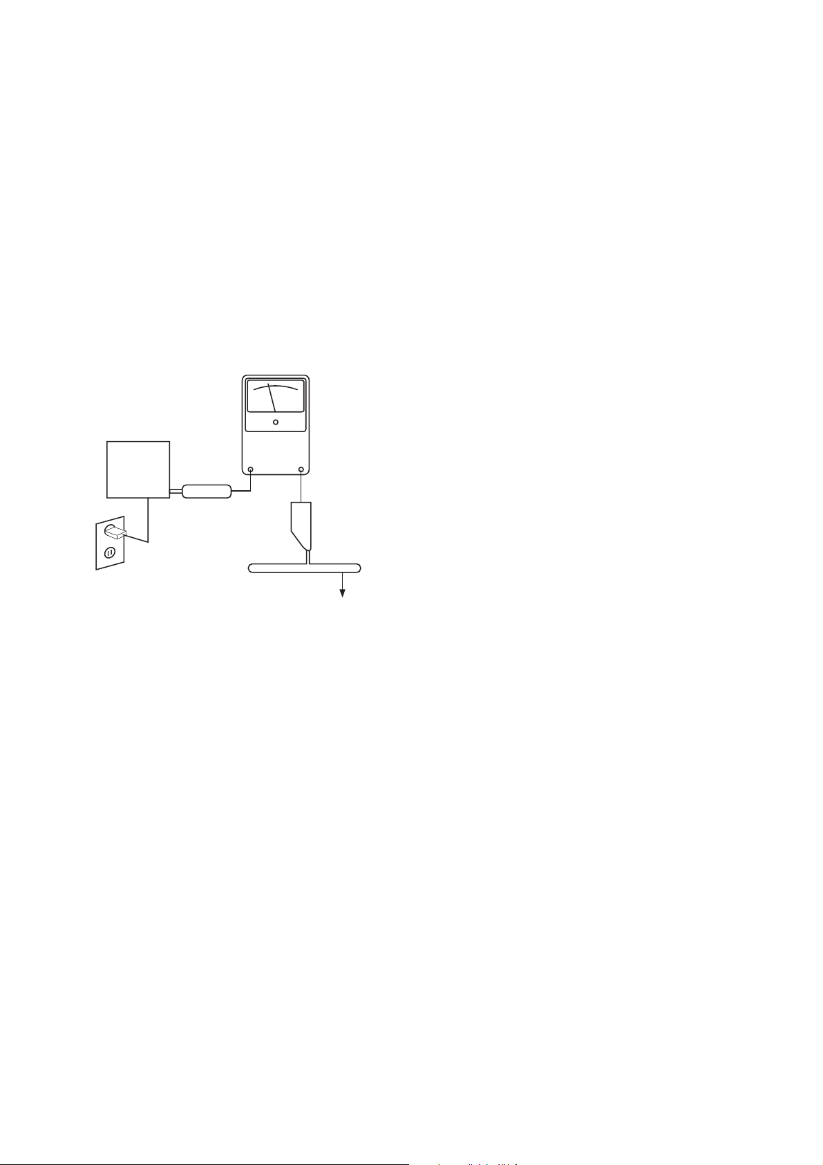
SAFETY PRECAUTIONS
The following check should be performed for the continued
protection of the customer and service technician.
LEAKAGE CURRENT CHECK
Measure leakage current to a known earth ground (water
pipe, conduit, etc.) by connecting a leakage current tester
between the earth ground and all exposed metal parts of the
appliance (input/output terminals, screwheads, metal
overlays, control shaft, etc.). Plug the AC line cord of the
appliance directly into a 120V AC 60Hz outlet and turn the
AC power switch on. Any current measured must not exceed
o.5mA.
Reading should
not be above
0.5mA
Device
under
test
Leakage
current
tester
Test all
exposed metal
surfaces
Also test with
plug reversed
(Using AC adapter
plug as required)
Earth
ground
AC Leakage Test
ANY MEASUREMENTS NOT WITHIN THE LIMITS
OUTLINED ABOVE ARE INDICATIVE OF A
POTENTIAL SHOCK HAZARD AND MUST BE
CORRECTED BEFORE RETURNING THE APPLIANCE
TO THE CUSTOMER.
Page 5
BDS 280S/580S
Installation Location
Moving the System
Before moving the system, rst disconnect it from the AC power and then remove the
interconnection cables to other components.
Cleaning
When the system gets dirty, wipe it with a clean, soft, dry cloth. After unplugging the
AC power cord, Wipe it with a soft cloth dampened with mild soapy water, then a fresh
cloth with clean water. Wipe it dry immediately with a dry cloth.
IMPORTANT: NEVER use benzene, aerosol cleaners, thinner, alcohol or any
other volatile cleaning agent.
NOTE: Do not use abrasive cleaners as they may damage the nish of metal
parts in the BDS system. Avoid spraying insecticide near the unit.
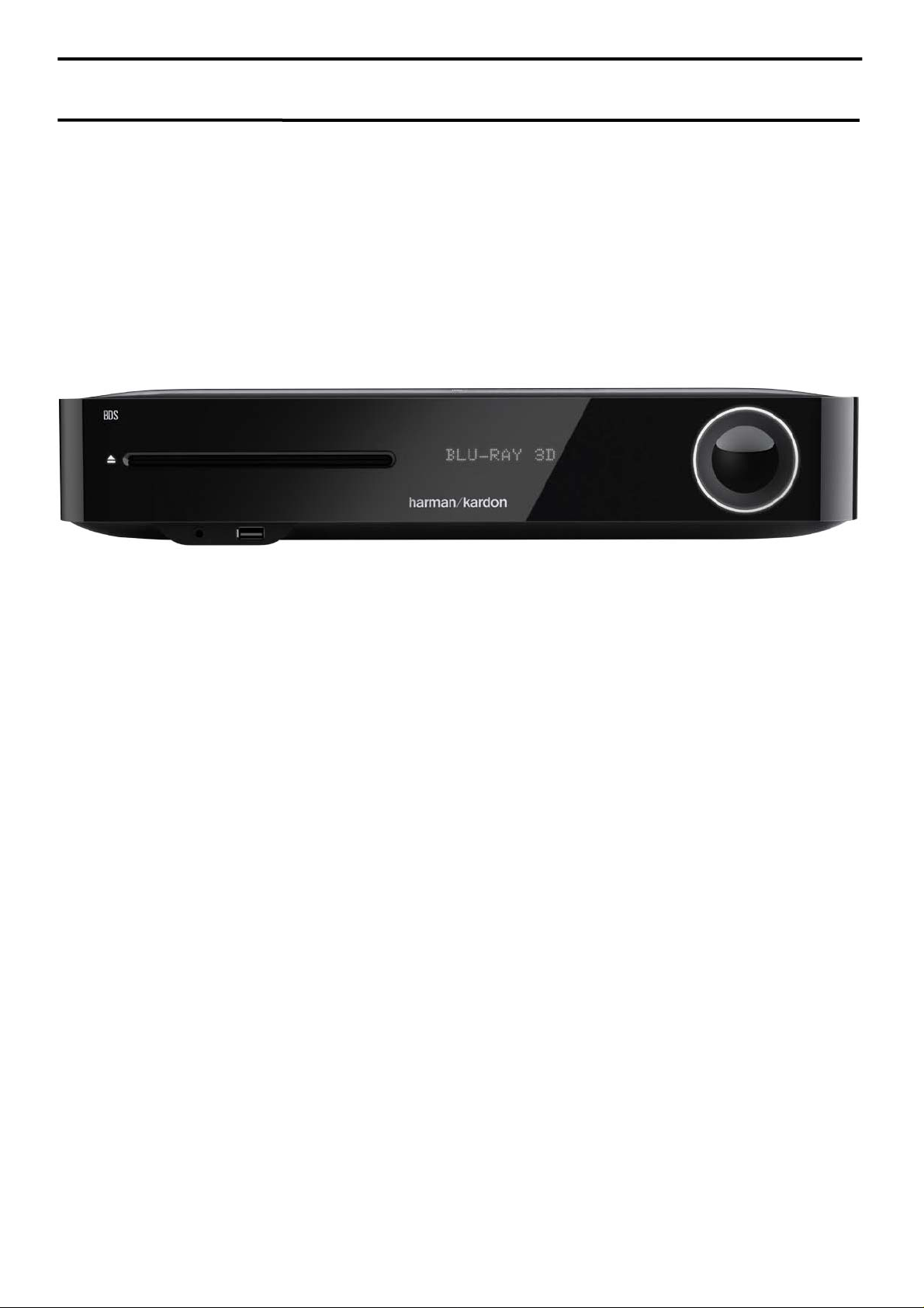
BDS Front Panel Controls and Connections
5
4
6
3
2
1. Disc slot
2. Headphone output and EzSet/EQ microphone input
3. USB/iPad/iPod/iPhone input
4. Volume ring and power button
5. NFC for Bluetooth pairing
6. Eject
7. Information display
1. Disc slot: Insert a compatible disc into the slot. The BDS system’s disc slot accepts
5-inch (12 cm) and 3-inch (8 cm) discs.
2. Headphone output and EzSet/EQ microphone input hcni-8/1 eht tresnI :
(3.5 mm) stereo mini connector from a set of headphones into this jack. When
performing EzSet/EQ speaker calibration, insert the microphone here.
NOTE: When a plug is inserted into the headphone jack, the BDS system’s
speaker output automatically becomes mute; the HDMI audio output
remains active.
3. USB/iPad/iPod/iPhone input: You can use the USB port to play audio les from
an Apple iOS device connected to the port, and to play audio les and show video and
picture les from a USB device inserted into the port. Insert the connector or device
into the USB port oriented so it ts all the way into the port. You may insert or remove
the connector or device at any time - there is no installation or ejection procedure. You
can also use the USB port to perform rmware upgrades. If an upgrade for the BDS
operating system is released in future, you will be able to download it to the BDS system
using this port. Complete instructions will be provided at that time.
IMPORTANT: Do not connect a PC or other USB host/controller to this port as
it may damage both the BDS system and the other device.
1
7
NOTE: This USB port is rated for 2.1A output, which suggests, it is certied
to charge iPad devices (as well as iPhone and iPod devices). There is a USB
connector on the rear panel as well with similar functionality, rated for
500mA to charge iPhone and iPod devices.
4. Volume ring and power button: Volume can be adjusted by touching this
capacitive ring. Slide clockwise around the ring to increase volume, counter-clockwise
to decrease volume.
IMPORTANT: If the audio from the speakers begins to distort at high volume
levels, reduce the volume as prolonged distortion can damage the system.
Page 6

BDS 280S/580S
BDS 280S/580S Rear Panel
Controls and Connections
Press this capacitive button to turn the BDS system ON. If the system is already ON, press
this button to push the system to Standby, Sleep or OFF mode.
The following table describes the dierent modes along with the LED display.
Mode Operation LED display
ON Press the power button White
Standby Long press on the power
button during Operational
mode (2.5 seconds)
OFF Switch OFF of the Rear
panel rocker switch
Sleep • No activity for
15 minutes in
operational mode,
Auto-standby ON
• Short press of
Power button from
Front panel during
operational mode
• Short press on the
remote control
power button or
power o command
from external IR or
remote app
Weak Amber
OFF
Amber
NOTE: While the system is powering on the volume ring will spin till the boot
process is complete.
5. NFC for Bluetooth pairing: Near Field Communication (NFC) is used for fast
Bluetooth pairing of compatible Android
mobile device near the NFC logo on the top front of the system to pair or unpair.
NOTE: The system can be brought to Operational mode from Sleep/Standby
mode by tapping on the NFC area.
6. Eject button (appears only when a disc has been inserted): Touch this button
to eject a disc from the BDS system’s built-in disc slot. Before touching this button, make
sure no objects block the disc-slot.
NOTE: If you do not remove the ejected disc within 30 seconds, it will
automatically re-load into the disc slot for protection.
7. Information display: Various messages appear on this display in response to
commands and to show the audio/video that is playing, the BDS system’s settings or
other aspects of the BDS system’s status as described throughout this manual.
TM
and Windows® mobile devices. Place the
BDS 280S/580S Rear Panel Controls and Connections
BDS 280
BDS 580
Page 7

BDS 280S/580S
BDS 280S/580S Rear Panel Controls and Connections
The following are the controls available in the rear panel of the BDS 280S/580S sytem:
1. Main Power Switch
2. AirPlay Antenna
3. Speaker outputs
4. Optical Digital Audio (S/PDIF) inputs
5. Trigger Output
6. AUX 1 input and AUX 2 input
7. Subwoofer output
8. Wi-Fi Antenna
9. FM radio antenna output
10. Coaxial digital audio (S/PDIF) input
11. IR Remote input
12. HDMI output (ARC)
13. HDMI 1/MHL input
14. HDMI 2 input
15. HDMI 3 (Apple) input
16. USB input
17. Network Connector
18. WPS button
19. AC Power input
1. Main Power Switch: This mechanical switch turns the BDS system’s power supply
ON or OFF. After you have made and veried all connections, set this switch to the ON
position. During normal use, you will usually leave this switch set to ON; it cannot be
turned ON or OFF using the remote control. To conserve energy when you are not using
the system for an extended period of time, set this switch to OFF.
2. AirPlay Antenna: Connect the antenna accessory labeled Antenna 1 here for
improved Wi-Fi reception. Connect the antenna accessory for the AirPlay playback from
the iPad/iPod/iPhone.
3. Speaker Outputs: Use the speaker wires supplied with the speakers to connect the
speakers to the proper terminals.
• The BDS 280 system has two outputs for left and right speakers.
• The BDS 580 system has ve outputs for center, front left, front right, surround left and surround right speakers.
4. Optical Digital (S/PDIF) Inputs: Connect the optical digital output of an audio
source component here. The signal may be a Dolby Digital, DTS® or standard PCM digital
audio.
5. Trigger Output: This connector provides 12V DC whenever the system is ON. It can
be used to turn on and o other devices such as a powered subwoofer.
6. AUX 1 and AUX 2 Input: Use these connectors to connect to an audio source device
(such as a tape deck). Do not connect a turntable to these connectors without a phono
preamp.
7. Subwoofer Output: Use a mono RCA audio cable to connect this jack to a powered
subwoofer’s line-level input or LFE jack.
8. Wi-Fi Antenna: Connect the antenna accessory labeled Antenna 2 here for
improved Wi-Fi reception.
9. FM Radio Antenna Output: Connect the supplied FM antenna to this terminal.
10. Coaxial Digital Audio (S/PDIF) Input: Connect the coaxial digital output of an
audio source component here. The signal may be a Dolby Digital bit stream, a DTS bit
stream or a standard PCM digital-audio bit stream.
11. IR Remote Input: When the IR sensor on the front panel is blocked (for example,
when the system is installed inside a cabinet); connect an optional IR receiver to the
Remote IR Input connector.
12. HDMI Output (ARC): Connect the BDS system’s HDMI output to your TV’s HDMI
input. If your TV is 3D capable, then you can watch 3D content in 3D either from the BDS
system’s built-in disc player or from other 3D-capable source devices connected to the
BDS system’s HDMI Input connectors (see below). The system’s HDMI output connection
also contains an Audio Return Channel (ARC) that carries a digital audio signal from
your TV or video display back to the BDS. It allows you to listen to HDMI devices that are
connected directly to your TV (such as a digital TV tuner) without making an additional
connection from the device to the BDS system.
NOTE: You must enable the ARC output of your TV. Consult your TV’s instruction manual for information.
13. HDMI Inputs: You can connect up to three additional source devices to the BDS
system provided the source devices have HDMI connectors. The HDMI connection
transmits digital audio and video signals between devices, so you do not have to
make any additional audio connections for devices you want to connect via an HDMI
connector. The BDS system will pass 3D video signals from 3D capable HDMI source
devices to the TV via the HDMI output connector.
Some HDMI inputs have special functionalities:
• HDMI 1/MHL input: This input accepts both HDMI and MHL connections.
MHL can be used with many mobile smart devices to mirror their audio
and video content on the BDS system while powering the device (check the
owner’s manual of your device). This connector is also compatible with the
Roku Streaming Stick, which allows access to Roku services, controlled by
the BDS remote control.
• HDMI 2 input: This input is a generic input port that accepts devices with
HDMI output. It helps in transmitting encrypted decompressed digital data
from the BDS system to the device connected to the BDS system.
• HDMI 3 (Apple) input: This input accepts any HDMI source device, but if
connected to Apple products, such as the Apple TV or Mac Mini, the BDS
remote can be used to control them (this input on the remote control is
pre-programmed with standard Apple device remote commands).
14. USB Input: You can use the USB port to play audio les from an Apple iOS device
connected to the port, and to play MP3 and WMA audio les and show video and
picture les from a USB device inserted into the port. Insert the connector or device
into the USB port oriented so it ts all the way into the port. You may insert or remove
the connector or device at any time - there is no installation or ejection procedure. You
can also use the USB port to perform rmware upgrades. If an upgrade for the BDS
operating system is released in the future, you will be able to download it to the BDS
system using this port. Complete instructions will be provided at that time.
IMPORTANT: Do not connect a PC or other USB host/controller to this port, or
you may damage both the BDS system and the other device.
7
Page 8
BDS 280S/580S
E
O
D
O
Remote Control Functions
NOTE:
• Apple devices should be connected only to the Front panel USB port
for the audio playback.
• This USB port is rated for 500 mA output and it suggests that
it is certied to charge iPhone and iPod devices. There is a USB
connector on the front panel as well with similar functionality,
rated for 2.1A to additionally charge iPad devices.
15. Network Connector: Use a Cat. 5 or Cat. 5E cable (not supplied) to connect the
BDS system’s Network connector to your home network to enjoy content from AirPlay,
DLNA, and streaming services, as well as control from the Harman Kardon Remote app
for iOS and Android. Additionally, system upgrades can be downloaded and installed
from compatible devices that are joined to the network.
16. WPS Button: You can connect to the Internet using the WPS button.
17. AC Power Input: After you have made and veried all other connections, plug the
supplied AC power cord into this input and into an unswitched AC outlet.
Remote Control Functions
HOM
UTTON
BUTTON
KEYBOAR
BUTTON
K
ACK
UTTON
CURSOR
NTROLS
C
PTIONS
BUTTON
Power Button: The BDS system has four dierent power modes:
• OFF (ON/Standby indicator not illuminated): When the rear-panel Main
Power switch is in the OFF position or the power cord is unplugged the BDS
system is o and will not respond to any commands. Plugging the power
cord into a live AC outlet and setting the Main Power switch in the On
position will put the system into the Standby mode.
• Standby (Power indicator glows weak amber): The Standby mode minimizes energy consumption when you are not using the BDS system. AirPlay
does not break-in with the unit in Standby mode. When the system is in
Standby, pressing the Power button turns it ON. To put the system into
Standby when it is ON, press the Power button for more than two seconds.
NOTE: To conserve energy you can have the system automatically enter the
Sleep mode whenever no control buttons have been pressed and no audio
signal has been present for 15 minutes.
• Sleep (Power indicator glows solid amber): The Sleep mode mutes the BDS
system’s outputs and shuts o its OSD and front-panel display, but allows
the system to automatically turn on and play audio in response to a signal
from an AirPlay device or a Bluetooth device. When the system is in Sleep,
pressing the Power button turns it on. To put the system into Sleep when it
is ON, press the Power button momentarily.
• ON (Power indicator glows solid white): When the BDS system is ON, it is
operational.
TV Power Button: After you program the remote control, pressing this button turns
the TV’s power ON and OFF.
Eject Button: Press this button to eject a disc from the BDS system’s built-in disc player.
Before pressing this button, make sure no objects are blocking the disc slot opening.
Source Buttons: Press one of these buttons to select a source device. This action will
also turn on the BDS system from the Standby mode.
• The rst press on the Aux button switches the BDS system to the last-used
of the sources such as Coaxial Digital, Optical Digital 1, Optical Digital 2,
Analog Audio I, Analog Audio 2, and HDMI ARC. Each successive press advances the BDS system through those sources. Pressing the Aux button also
places the remote into the auxiliary-component control mode, enabling the
remote to use any pre-programmed and/or learned functions.
NOTE: You must use the Home menu to select network-based sources (DLNA,
Pandora® and Picasa™).
Pop-Up Button: Pressing this button while playing a Blu-ray Disc recording or DVD
displays its disc menu.
NOTE: This feature is disc-dependent. Not all DVDs have pop-up menus. If a
DVD has no pop-up menu, pressing the Pop-Up button may display the disc
menu, depending on how the disc’s menu system is authored.
Page 9
BDS 280S/580S
Setting up the System
Erasing a Learned Code and Restoring the Original Button Code
1. Press and simultaneously hold down the Aux and Bookmark (green)
buttons on the BDS remote control for at least three seconds. The BDS
remote will enter the learning mode after the Aux button LED turns on.
2. Press and release the remote control button that you want
to erase. The aux button’s LED will ash three times.
3. To erase other buttons, press the selected buttons.
4. To exit the erase mode, press aux button.
Resetting the Remote to Factory Default Condition
1. Press and simultaneously hold down the Aux and Thumbnail (yellow)
buttons on the BDS remote control for at least three seconds.
2. The Aux LED will ash three times and exit learn-erase mode.
NOTE:
• By erasing all learned codes, all of the BDS remote buttons will
return to their original functions.
• To program the remote control for TV device, please use the TV
button instead of AUX button.
Controlling an Apple TV
If you have connected an apple TV to the BDS system’s HDMI 3 input, you can also use
the BDS remote to control an apple TV that is streaming audio and video les stored on
your home network, or accessing media from an Internet service such as Netix.
Select any other input source to return the BDS remote to its normal operation.
NOTE: To program the remote control for TV device, please use the TV button
instead of AUX button.
1. When you turn on your BDS system for the rst time, the onscreen menu will show the Initial Setup screens. The rst
screen allows you to select the language you want to use.
2. Press OK, and the initial setup Resolution screen will be displayed.
3. Highlight your choice and press OK. Next, the initial setup Aspect Ratio
screen will appear. 16:9 Full is the best choice for most displays.
Using the Remote after it is Programmed
Pressing the remote’s Aux Input button will put the remote into the auxiliarycontrol mode, and it will control the auxiliary component(s) via the codes you have
programmed into it.
If you have programed a TV with TV button, you can press remoter’s TV button to put
the remote into TV control mode and it will control the TV via the codes you have
programmed into it.
To switch the remote back to the BDS system-control mode from the auxiliary-control
mode, press any of the other Input buttons or the Home button.
Setting up the System
To set up your BDS system, you will use the remote to navigate through all of the
onscreen menus and to make selections from them.
• Use the Cursor Up/Down buttons to navigate through the menu list.
• To select a highlighted item, press the OK button. The screen will change
depending on your selection.
• To return to the previous screen, press the back button
NOTE: BDSx80 CR3 software will have advanced intial setup, which means
the setup procedure will be dierent with current one at that time.
.
4. Highlight your choice and press the OK button. Setup is complete. Press
OK once more to nish Initial Setup and show the home menu.
15
Page 10

BDS 280S/580S
Troubleshooting
Troubleshooting
Problems Solutions
The system does not power up (the Power indicator is not lit) • Check whether the system’s Power cord is properly plugged into the
system’s AC Power connector.
• Check that the Power cord is plugged into a working AC outlet. If the
outlet is controlled by a switch, make sure the switch is set in the ON
position.
• Check that the system’s main power switch (located on the rear panel)
is in ON position.
Sound plays through the speakers, but there is no TV picture • Check the HDMI connection between the system and the TV.
• Check the HDMI connection or Component Video connection between
the source device and the BDS system.
• Check that the TV is turned on and is set to the proper input source.
• Unplug the HDMI cable from the TV and plug it back in again.
There is no sound coming from just the subwoofer • Check that the subwoofer’s Power cord is plugged into a working AC
outlet.
• Check that the subwoofer’s power switch is in the ON position.
• Check that the Subwoofer Level control is not turned all the way down
(fully counter clockwise).
• Check that the audio connection between the system and the subwoofer
has been properly made.
• Check the system’s Settings: Conguration menu to make sure that the
subwoofer volume has not been set at 10dB.
There is a constant hum in the sound • Check that all input cables are plugged all the way into their connectors.
• Check that all cables are at least 10 ft (3.3m) from uorescent lights.
• Check that all cable connectors are clean. If necessary, wipe them with a
cloth slightly moistened with alcohol.
• Set the subwoofer’s power switch to OFF. If the hum goes away, there
is a ground loop between the subwoofer and the system. Plugging
the subwoofer’s power cord into the same AC outlet that the system is
plugged into should eliminate the ground loop.
21
Page 11

BDS 280S/580S
Troubleshooting
Troubleshooting
Problems Solutions
The system does not power up (the Power indicator is not lit) • Check whether the system’s Power cord is properly plugged into the
system’s AC Power connector.
• Check that the Power cord is plugged into a working AC outlet. If the
outlet is controlled by a switch, make sure the switch is set in the ON
position.
• Check that the system’s main power switch (located on the rear panel)
is in ON position.
Sound plays through the speakers, but there is no TV picture • Check the HDMI connection between the system and the TV.
• Check the HDMI connection or Component Video connection between
the source device and the BDS system.
• Check that the TV is turned on and is set to the proper input source.
• Unplug the HDMI cable from the TV and plug it back in again.
There is no sound coming from just the subwoofer • Check that the subwoofer’s Power cord is plugged into a working AC
outlet.
• Check that the subwoofer’s power switch is in the ON position.
• Check that the Subwoofer Level control is not turned all the way down
(fully counter clockwise).
• Check that the audio connection between the system and the subwoofer
has been properly made.
• Check the system’s Settings: Conguration menu to make sure that the
subwoofer volume has not been set at 10dB.
There is a constant hum in the sound • Check that all input cables are plugged all the way into their connectors.
• Check that all cables are at least 10 ft (3.3m) from uorescent lights.
• Check that all cable connectors are clean. If necessary, wipe them with a
cloth slightly moistened with alcohol.
• Set the subwoofer’s power switch to OFF. If the hum goes away, there
is a ground loop between the subwoofer and the system. Plugging
the subwoofer’s power cord into the same AC outlet that the system is
plugged into should eliminate the ground loop.
21
Page 12

4‐1
Software Upgrade
1.The upgrade image file name shall be:
BDS 280S: HK_BDS280S.bin
BDS 580S: HK_BDS580S.bin
2. BDS has two kinds of upgrading method:
2.1: Use USB to upgrade:
1) Create a new folder which name “UPG” in the root directory of the USB,and copy
the upgrade file into the “UPG” folder;
2) Plug in the USB;
3)Press “HOME” button from remote control to entering the HOME menu, choose the
“Setting” option from HOME menu, and then choose “System”Æ”System upgrade”
Æ”USB” in sequence, then press “OK” button from remote control, BDS will start to
upgrade.
2.2: Upgrade online:
1) Please ensure that your network is smooth.(Wired or wireless);
2)Press “HOME” button from remote control to entering the HOME menu, choose
the “Setting” option from HOME menu, and then choose “System”Æ”System upgrade”
Æ”internet” in sequence, then press “OK” button from remote control, BDS will start to
upgrade.
Page 13
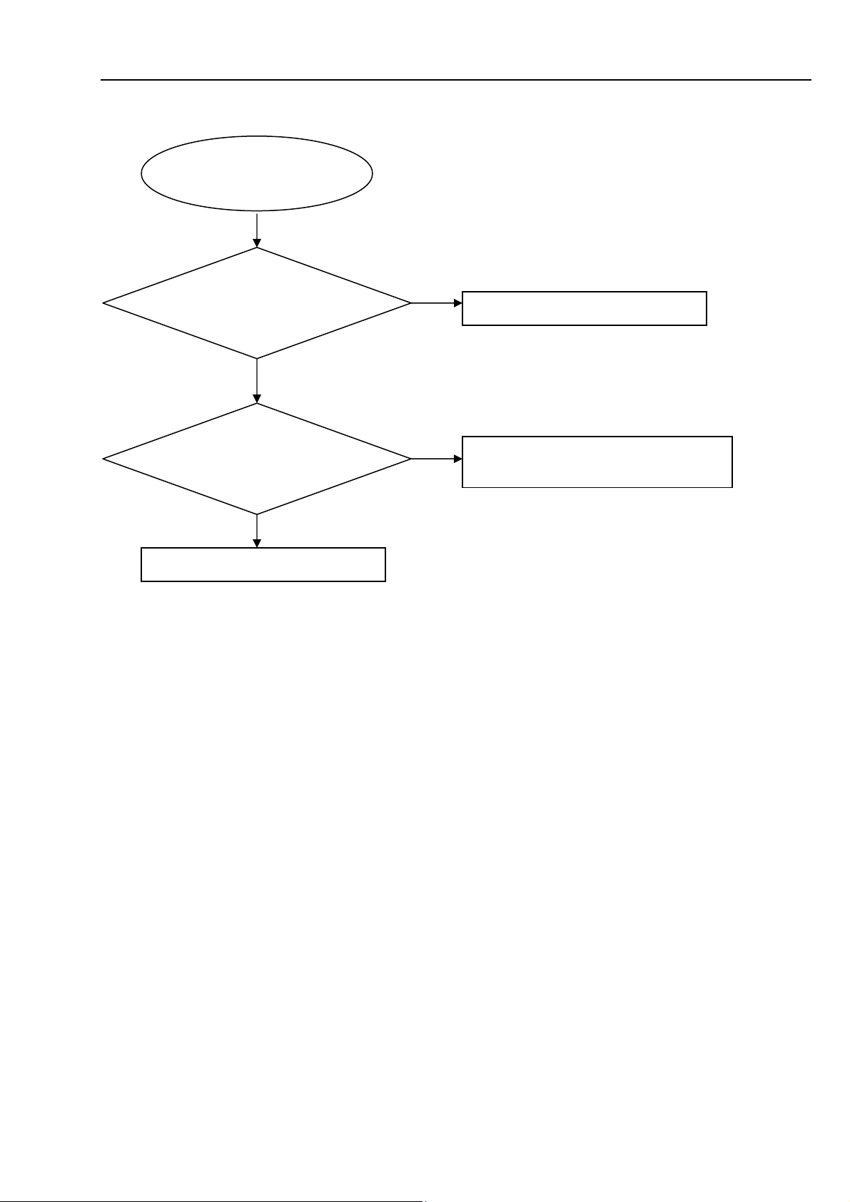
5-1 Trouble shooting Chart
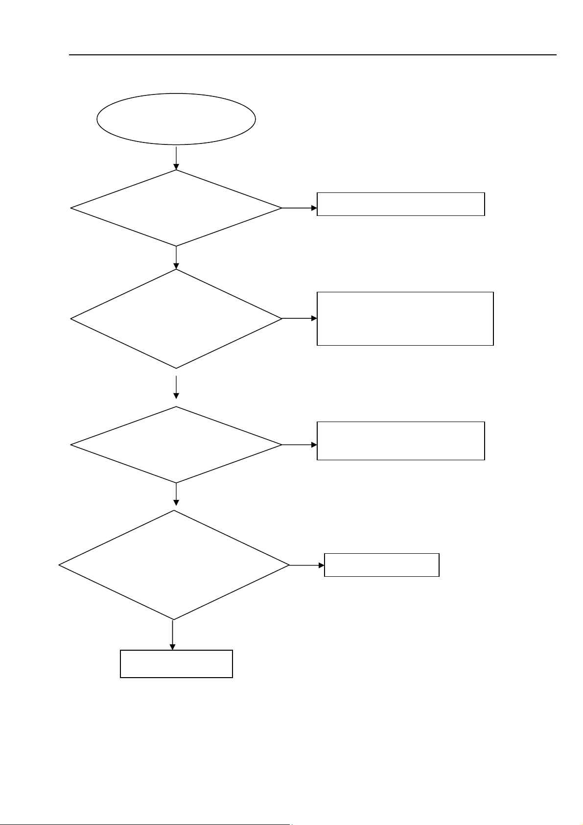
Power on led doesn't work
Power on led doesn't
work
GO
Switch performance
check
NG
Change switch
OK
Check the cable XP504 is
connect well to Main board
XP6
NG
Reconnect the cable
OK
Check+5V,+12V,VCC_D
voltage on the power and
Main board
NG
Refer to Power supply board part
OK
Check the power on led
control circuit is OK
NG
Replace the FB
Replace the LED25---LED31
OK
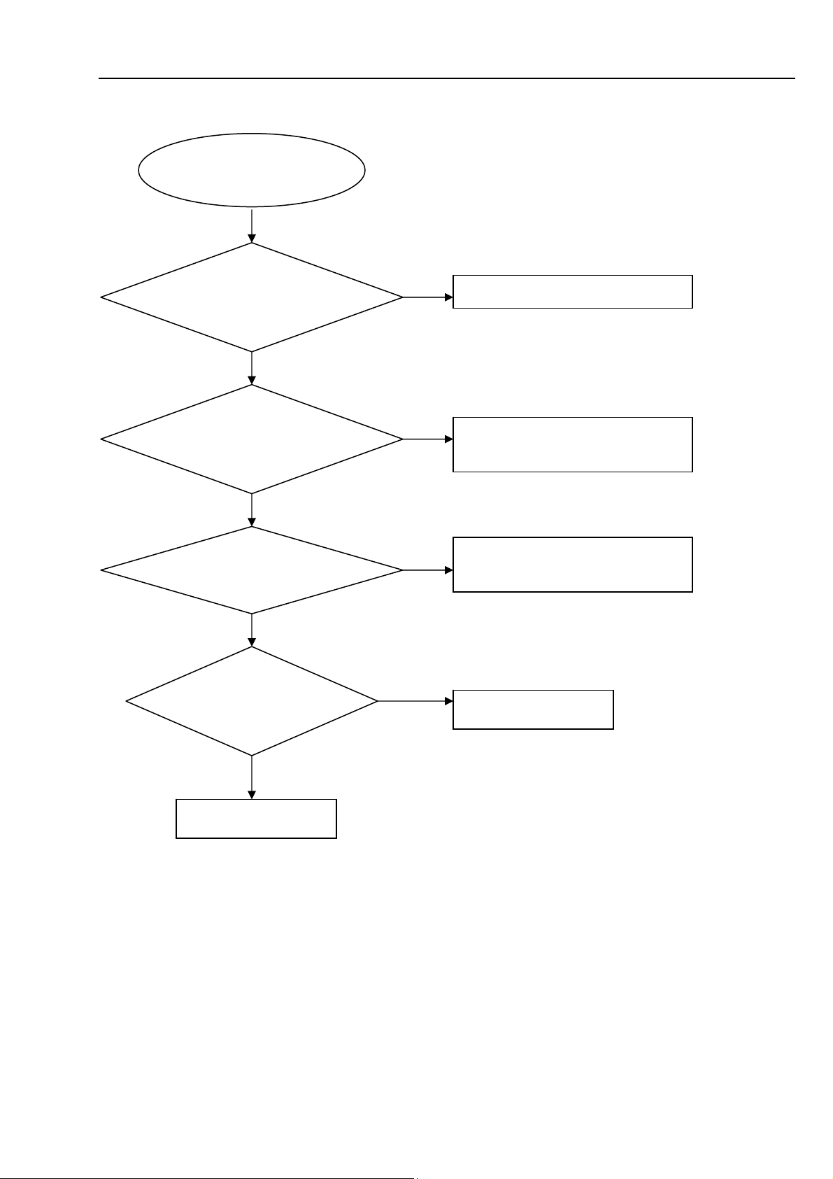
Page 14
No display on VFD
No display on VFD
Check every supply
voltage on Main board is
normal
Check+5V,+12V,VCC_D
voltage on the power and
Main board and 38V on
FB Board
Yes
Check the front board
signals VDIN,VCLK,
VSTB
1.Check whether bad
solder exists on pins of
VFD,
Yes
Replace VFD or FB
Go
Yes
Yes
5-2 Trouble shooting Chart
No
Refer to Power supply board part
No
No
Fix the connection XP4 on Main board
and CON503 on power board, and
24pin FFC cable from FB to Main board
Check the U701 pin 31,32,34 arrive the
condition XP504 13,12,11
No
Correct connection
Page 15
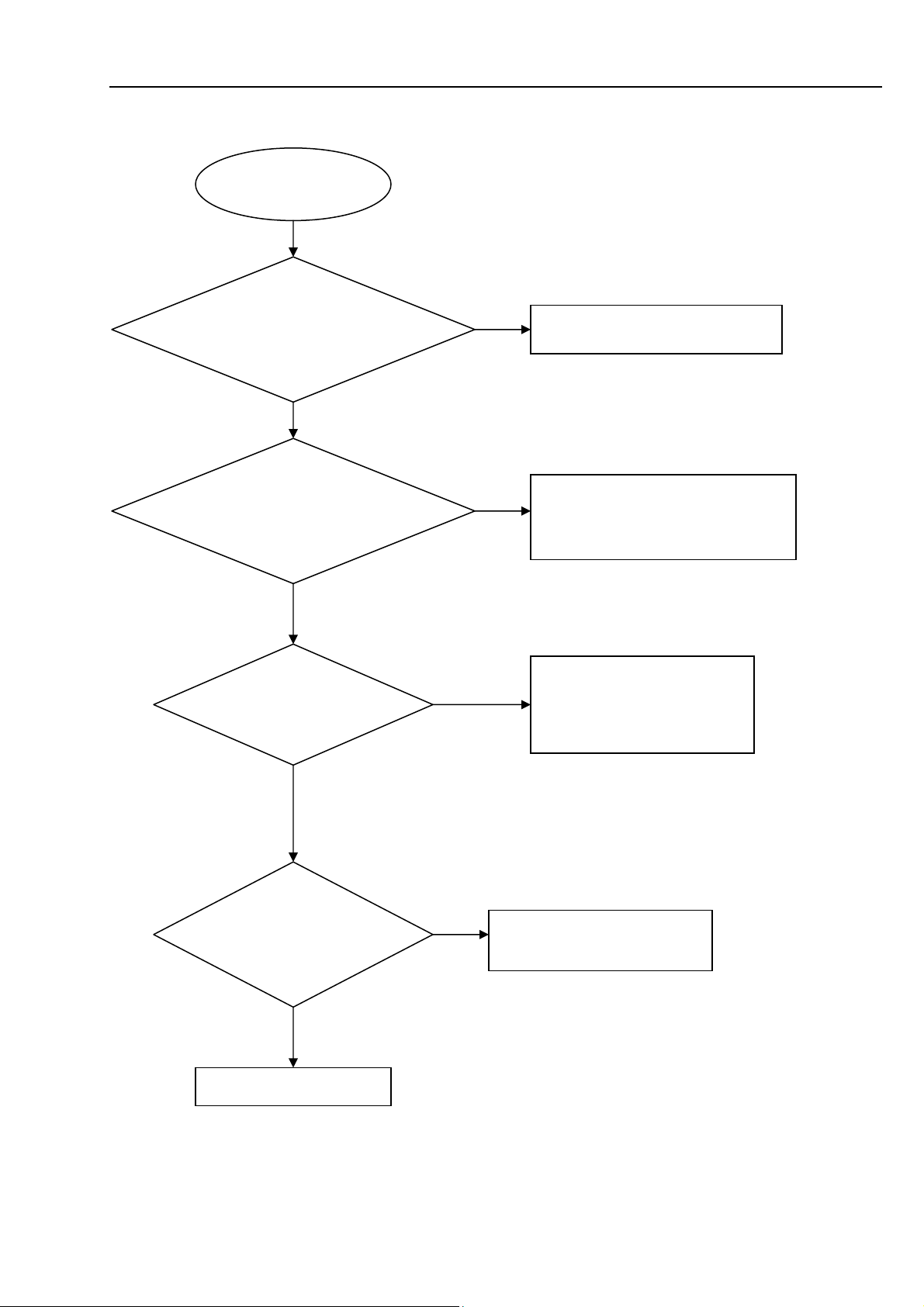
Remote control does not work
Remote control
does not work
Go
Check whether the remote
controller’s battery is
exhausted or not.
Yes
Check the 24pin FFC cable
from FB to Main board is
connect well
Yes
Check the IR501 power
supply is OK, IR501 pin3 is
about 3.3V
Yes
Replace IR501
5-3 Trouble shooting Chart
No
No
No
Replace the battery for remote
controller
Reconnect the cable
Check the +3.3V net on front board
Page 16
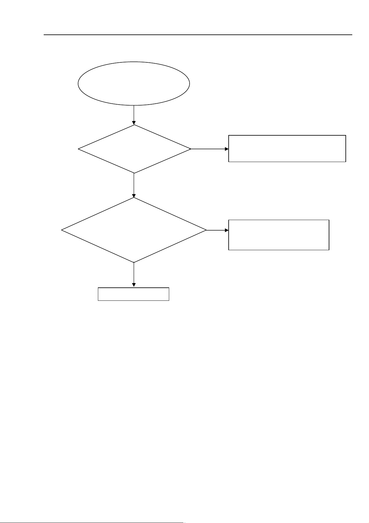
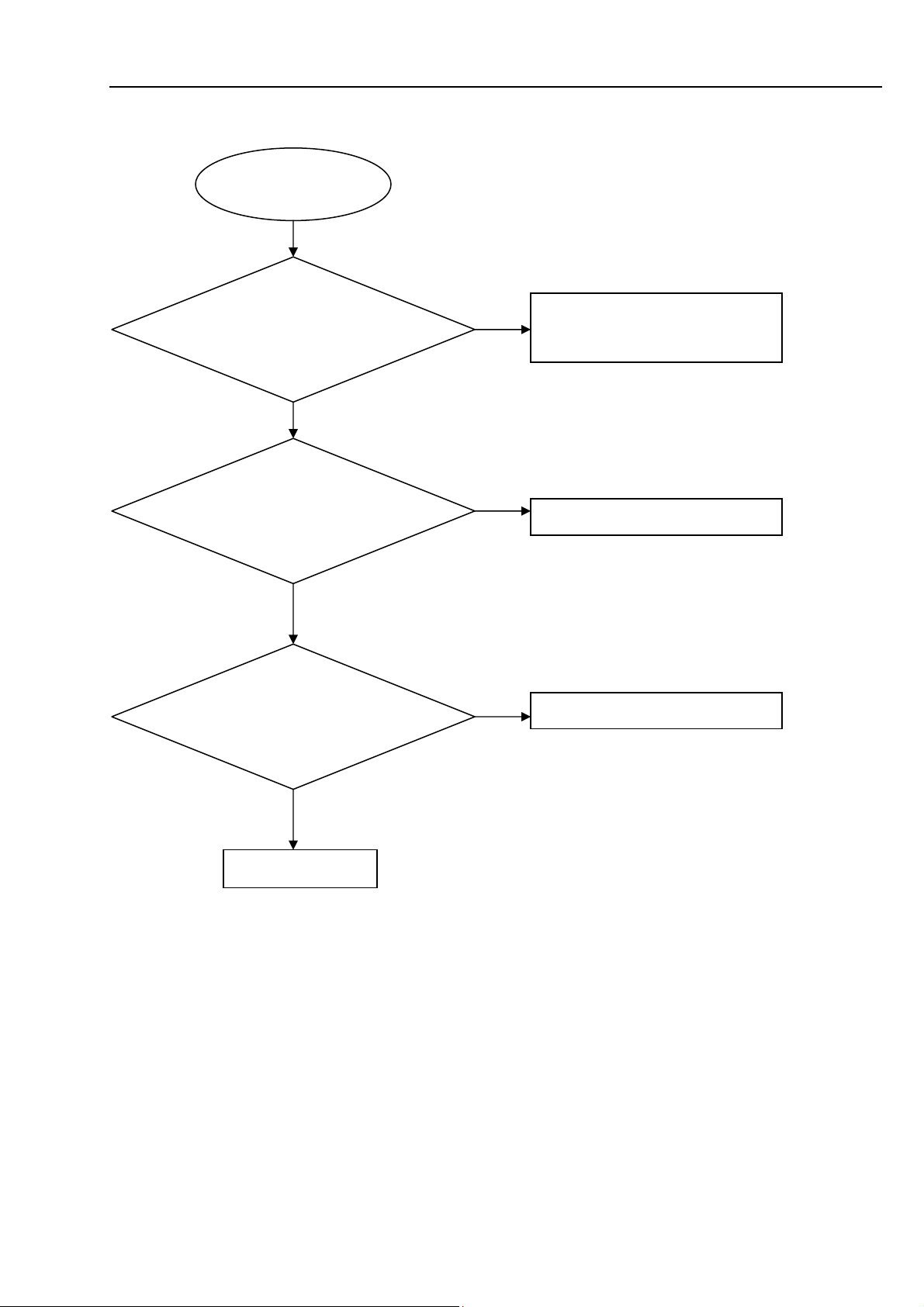
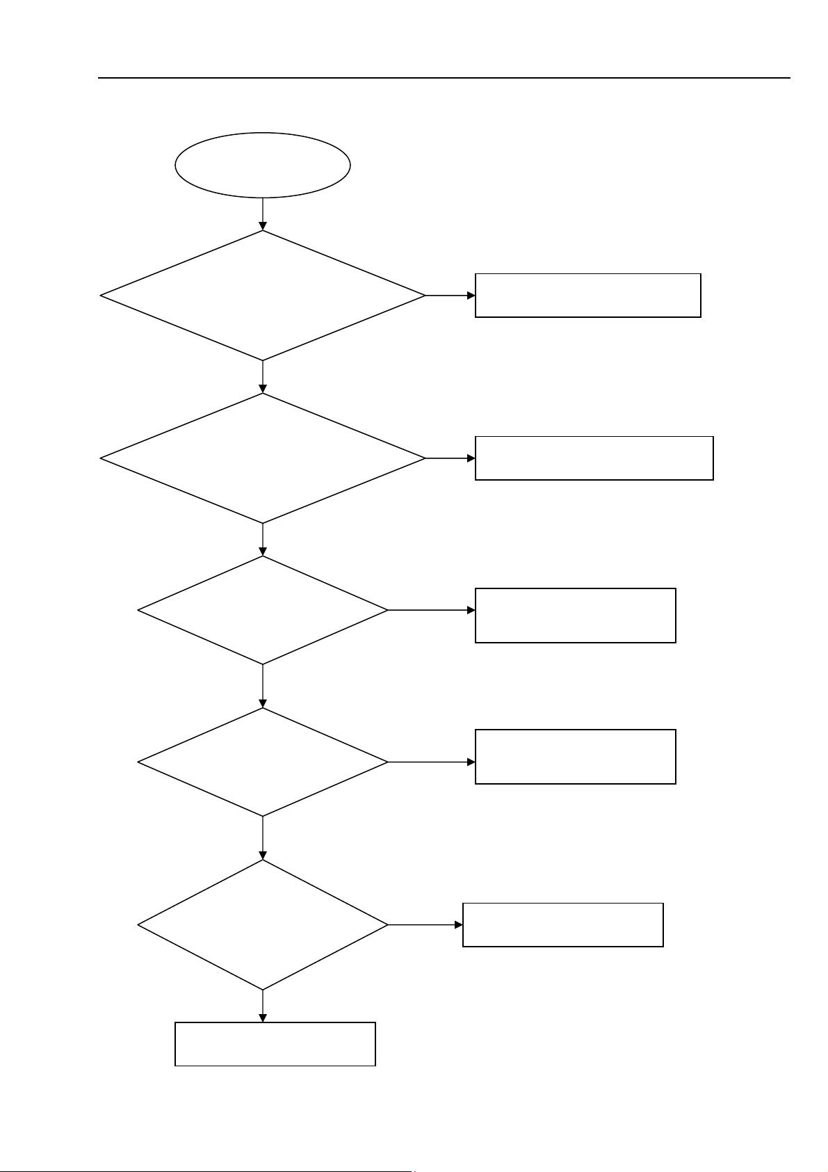
Can’t read disc or can’t eject
Can’t read disc or can’t
eject
GO
Check whether the
DVD loader running is
normal
Yes
Check 45pin and 5pin/9pin
cable from Main board
connection to the loader is
normal
Yes
Replace the Main board
5-4 Trouble shooting Chart
NO
NO
Check the connection 5pin cable from the
BD board
Fix the connection the 45pin cable
and 5pin/9pin cable
Page 17
5-5 Trouble shooting Chart
p
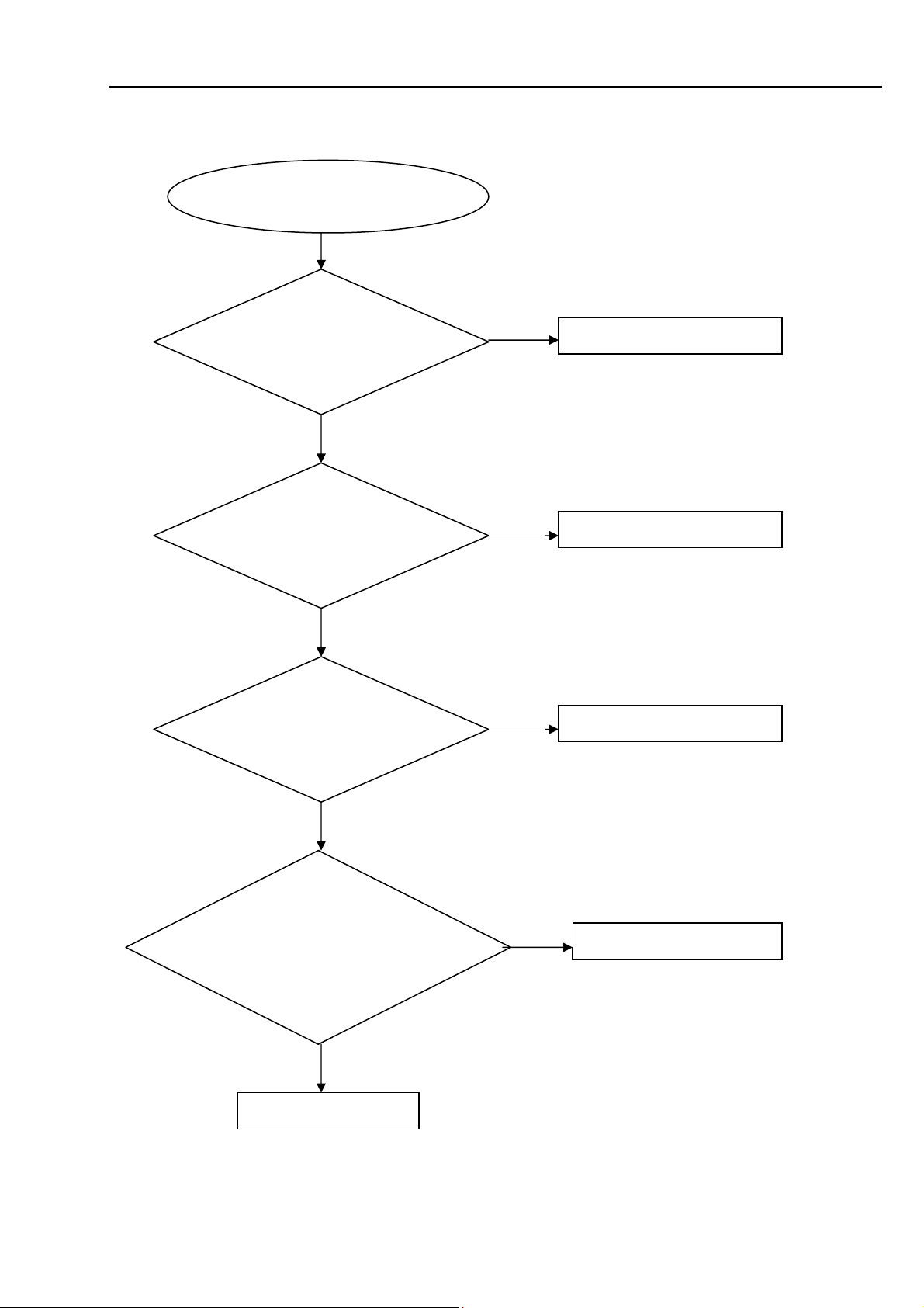
5.1/2.1 channel no audio output
5.1/2.1 channel no audio
ut
out
Go
Check the 10pin/4pin cable is
connect well from Main board to
AV board
No
Reconnect well
Yes
Check XP27 is short to
GND
Yes
Replace the Main board
No
Check +32V at XP27 on
Main board is OK
No
Refer to Power supply board
Yes
check the system weather is
headphone mode or not, pull
out the 6pin cable XP26 from
USB to Main board
No
Replace the Main board
Yes
Replace the USB board
Page 18
BD/DVD/CD no audio output
p
BD/DVD/CD no audio
output
Go
Check HDMI audio is ok
Yes
Check the audio of
COAXIAL mode is OK
Replace the Main Board
Yes
5-6 Trouble shooting Chart
No
No
Replace the Main Board
Next acting as the problem 5.1/2.1
channel no audio out
ut
Page 19
Tuner FM does not work
Tuner FM does not work
Go
Check the DVD mode is
OK,audio output is ok
Yes
Check Tuner module
pin5 supply voltage is
+3.3V
Yes
Check Tuner module
pin7,pin8,L/R output
Yes
Check the U203 is
working normal
Yes
Replace Main Board
5-7 Trouble shooting Chart
No
Replace the Main board
No
No
No
Check Main board tuner voltage supply
circuit.
Change the Tuner module
Replace U203
Page 20
AUX in does not work
AUX in does not
work
Go
Check the DVD mode is
OK,audio output is ok
Yes
Check the Main board
U203 AK5367 PIN2,PIN3,
PIN6,PIN7 L/R signal input
Yes
Check the U203
AK5367
PIN30,VDD+5V,
Yes
Check U203
AK5367 is broken.
Yes
Replace U203 AK5367
5-8 Trouble shooting Chart
No
Replace the Main board
No
No
No
Check the main board R221—R224
and C284,C286,C288,C290
Check the main board U203
power supply circuit
Check the U28
Page 21
IPOD in does not work
IPOD in does not
work
Go
Check the DVD mode is
OK,audio output is ok
Yes
Check whether USB can
work well on front USB port
Yes
Check whether the
USB Switch U43 is
work well
Yes
Check whether the
CP IC U44 is work
well
Yes
Check MCU U21 is
work well
Yes
Check the I2S Switch U26
5-9 Trouble shooting Chart
No
Replace the Main board
No
No
No
No
Replace the USB board
Replace U43
Replace U44
Replace U21
Page 22

COAX/OPTICAL does not work
COAX/OPTICAL
does not work
Go
Check the DVD mode is
OK,audio output is ok
Yes
Check the coax/optical
connector is ok
Yes
Check U23
PIN3,PIN22 +3.3V
Yes
Check U23 CS8422
is broken.
Yes
Replace U23 CS8422
5-10 Trouble shooting Chart
No
Replace the Main board
No
No
No
Replace the connector
Check the main board U23
power supply circuit
Check the U28
Page 23

Fan can not rotate
p
FAN can not rotate
Go
Check the voltage
of FAN
OK
Replace a new fan
HDMI input does not output
HDMI input does
not out
ut
Go
check connector is HDMI IN 1,
AND SET HDMI IN 1 INPUT,
Yes
OK
Check the DVD mode is
OK,HDMI output is ok
OK
Replace U27 Sil9573
5-11 Trouble shooting Chart
No
Check the FAN
power supply circuit
No
No
Correct connection
Replace the Main board
Page 24

WIFI or Airplay does not work
O
WIFI or Airplay does not
work
Go
Check the WIFI module
and antenna is OK
OK
Check the Airplay
module and antenna is
K
Replace the Main board
OK
5-12 Trouble shooting Chart
NO
Replace the WIFI
Module or antenna
NO
Replace the Airplay
Module or antenna
Page 25

BT does not work
O
BT does not work
Check the BT antenna
is OK
Check the FB board is
OK
OK
Go
OK
5-13 Trouble shooting Chart
NO
Replace the BT
antenna
NO
Replace the FB
Board
Check the 24pin FFC
with connect Main
Board to FB board is
K
OK
Replace the Main board
NO
Replace the 24pin
FFC
Page 26

6-1 6-1
Page 27

A
7-1 7-1
Harman Kardon
BDS 280 + 580 Service Manual
Page 38 of 87
USB Board Circuit Diagram:
5
R601 0R601 0
C600
9PIN/H-CKX-3.5-12
9PIN/H-CKX-3.5-12
D D
GND
GND
GND
GND
SGND
GND
GND
P600
P600
1
9
8
7
3
2
SIN
4
5
6
DET
TP600TP600
TP601TP601
TP602TP602 R611 0R611 0
TP603TP603
TP604TP604
C600
0.01uF/50V/Y5V
0.01uF/50V/Y5V
0.01uF/50V/Y5V
0.01uF/50V/Y5V
C612
C612
100K
100K
R604
R604
R614
R614
100K
100K
4
HP_R
C601
C601
0.1uF/50V/Y5V
C609
C609
0.1uF/50V/Y5V
C610
C610
0.1uF/50V/Y5V
0.1uF/50V/Y5V
1K
R6221KR622
Q600
Q600
PNP_3CG3906M
PNP_3CG3906M
R625
R625
100K
100K
-5V
4.7uF/50V/Y5V
4.7uF/50V/Y5V
C633
C633
+5V
+5V
R607 1KR607 1K
C607
C607
10uF/10V/Y5V
10uF/10V/Y5V
MIC_CT
R638
R638
4.7K
4.7K
R6101KR610
1K
C608
C608
䴴䖥
10uF/10V/Y5V
10uF/10V/Y5V
1K
R626
R626
100K
100K
+2.5V
IC
0.1uF/50V/Y5V
0.1uF/50V/Y5V
R6211KR621
R624
R624
100K
100K
5A3159
5A3159
TS
TS
4
COM
5
V+
6
IN
U600
U600
U602
U602
6
IN
5
V+
4
COM
S
S
5A3159
5A3159
T
T
+5V
R619 5.6KR619 5.6K
3
C605
C605
0.1uF/50V/Y5V
0.1uF/50V/Y5V
C606
C606
HP_ROUT
R605 4.7KR605 4.7K
R609
R609
4.7K
4.7K
HP_LOUT
GND
GND
R600 20R600 20
3
NC
2
1
NO
1
NO
2
3
MIC_IN
NC
4.7K
4.7K
R620
R620
R615
R615
2.2K
2.2K
C602
C602
0.1uF/50V/Y5V
0.1uF/50V/Y5V
C611
C611
0.1uF/50V/Y5V
0.1uF/50V/Y5V
R616 20R616 20
C615
C615
10uF/10V/Y5V
10uF/10V/Y5V
10uF/10V/Y5V
10uF/10V/Y5V
2
USB5V
-5V
USB_EN
USB_EN
R606 NC/10KR606 NC/10K
USB5V
R617 NC/10KR617 NC/10K
R602 NC/100KR602 NC/100K
U601
U601
1
IN
2
GND
EN3FLAG
NC/MP65150
NC/MP65150
R612 NC/100KR612 NC/100K
U603
U603
1
IN
2
GND
EN3FLAG
NC/MP65150
NC/MP65150
OUT
ILIM
OUT
ILIM
6
5
4
NC/15K/1%
NC/15K/1%
6
5
4
NC/15K/1%
NC/15K/1%
R608
R608
R618
R618
1
R603 NC/4.7KR603 NC/4.7K
C603
C603
10uF/10V/Y5V
10uF/10V/Y5V
R613 NC/4.7KR613 NC/4.7K
C613
C613
10uF/10V/Y5V
10uF/10V/Y5V
USB_OC
USB_POWER
USB_OC
USB_POWER
C604
C604
0.1uF/16V/Y5V
0.1uF/16V/Y5V
C614
C614
NC/0.1uF/16V/Y5V
NC/0.1uF/16V/Y5V
C C
R627
R627
68K
68K
R629
R629
10K
10K
Q602
Q602
NPN_MMBT8050C
NPN_MMBT8050C
B B
4PIN/2.0mm/180mm
4PIN/2.0mm/180mm
XP602
XP602
TO MAIN PCB
4
3
2
1
4
3
2
1
+5V
C616
C616
1000pF/50V/X7R
1000pF/50V/X7R
R631
R631
10K
10K
TP615TP615
HP_DET
C624
C624
0.1uF/50V/Y5V
0.1uF/50V/Y5V
TP616TP616
TP617TP617
HP_DET
HP_ROUT
HP_LOUT
8
8
7
7
6
6
5
5
4
4
3
3
2
2
1
1
8PIN/2.0mm/100mm
8PIN/2.0mm/100mm
XP26
XP26
+12V_D
MIC_IN
VCC_D
U605
U605
A
6
4
6
VCC
Shell B
D+
GND
Shell A
5
USB-A/WT
USB-A/WT
1000pF/50V/X7R
1000pF/50V/X7R
D-
P601
P601
USB_POWER
1
2
3
4
L600 NCL600 NCR685 0R685 0
FB
C645
C645
R683
R683
10K
10K
TP605TP605
C622 0.01uFC622 0.01uF
L601 NCL601 NC
A
SK34/40V/3A
SK34/40V/3A
D600
D600
USB_DP
TP606TP606
USB_DN
TP608TP608
TP610TP610
ESD600
ESD600
2 1
L602 33uH/3AL602 33uH/3A
R64910R649
10
C644
C644
1000pF/50V/X7R
1000pF/50V/X7R
2 1
10180Z020
10180Z020
+12V_D
ESD601
ESD601
10180Z020
10180Z020
C625
C625
0.1uF/50V/Y5V
0.1uF/50V/Y5V
1
2
XP601
XP601
2PIN/2.5mm/90mm
2PIN/2.5mm/90mm
TO POWER PCB
R650
R650
43K
43K
C632
C632
+
+
10uF/10V/Y5V
10uF/10V/Y5V
R657
R657
10K/1%
10K/1%
TP607TP607
TP609TP609
TP611TP611
TP612TP612
1
2
2.1A
CE600
CE600
220uF/16V
220uF/16V
4
4
3
3
2
2
1
1
4PIN/2.0mm/100mm
4PIN/2.0mm/100mm
TO MAIN PCB
TP613TP613
TP614TP614
USB5V
C643
C643
0.1uF/16V/Y5V
0.1uF/16V/Y5V
XP600
XP600
R693
R693
39K/1%
39K/1%
R691
R691
2.7K/1%
2.7K/1%
R689
R689
9.1K/1%
9.1K/1%
C631
C631
1uF/50V/Y5V
1uF/50V/Y5V
R644 0R644 0
R645 0R645 0
34V
USB_POWER
R630
R630
27K
27K
C627
C627
DS
G
R705
R705
10K
10K
R702
R702
4.7K
4.7K
NPN_3CG3904M
NPN_3CG3904M
REFM+12V_MIC
C620
C620
10uF/16V/X7R
10uF/16V/X7R
R704
R704
10K
10K
Q606
Q606
R703
R703
4.7K
4.7K
C619
C619
1000pF/50V/X7R
1000pF/50V/X7R
R635 4.7KR635 4.7K
FB601 120/2AFB601 120/2A
C668
C668
1000pF/16V
1000pF/16V
R707 1KR707 1K
C666
C666
100pF/50V/NP0
100pF/50V/NP0
C629
C629
470pF/50V/NP0
470pF/50V/NP0
Q604
Q604
PNP_3CG3906M
PNP_3CG3906M
34V_D
R6521KR652
1K
R695 220R695 220
R697
R697
560
560
C623 47pF/50V/NP0C623 47pF/50V/NP0
R633 68KR633 68K
F4558
F4558
-
-
6
U604B
U604B
7
+
+
5
8 4
+12V_MIC
R641
R641
22K
22K
REFM
ZD600
ZD600
USB5V
BZV55C5V1/5.1V
BZV55C5V1/5.1V
C628
C628
4.7uF/16V/Y5V
4.7uF/16V/Y5V
MIC_OUT
R637
R637
100K
100K
34V_D
47uF/50V
47uF/50V
CE601
CE601
20120925 change CE612
C659
C659
0.01uF/50V/Y5V
0.01uF/50V/Y5V
+
+
Y5V
Y5V
1uF/50V/
1uF/50V/
C638
C638
C639
C639
R686 0R686 0
5
3
FB
SW
1
BS
COMP
IN
GND
2
OVEN
OCSET
8
7
EUP3453
EUP3453
C640
C640
R658
R658
200K
200K
50V/X7R
50V/X7R
50V/X7R
50V/X7R
0.1uF/
0.1uF/
0.1uF/
0.1uF/
R634
R634
4.7K
4.7K
C630
C630
100pF/50V/NP0
100pF/50V/NP0
MIC_OUT
HP_DET
MIC_CT
USB_EN
USB_OC
R628 27KR628 27K
C618
C618
0.1uF/50V/Y5V
0.1uF/50V/Y5V
+12V_D
R640
R640
22K
22K
REFM
D601 SS24/40V/2AD601 SS24/40V/2A
34V
D602 SS16/60V/1AD602 SS16/60V/1A
C621 47pF/50V/NP0C621 47pF/50V/NP0
R632 68KR632 68K
-
-
2
1
+
+
3
U604A
U604A
10uF/10V/Y5V
10uF/10V/Y5V
F4558
F4558
8 4
+12V_MIC
Av=(68/5.1)*(68/5.1)=45dB
R646 0R646 0
R643 10KR643 10K
Q603 AP2305Q603 AP2305
R699 4.7KR699 4.7K
Q605
Q605
NPN_3CG3904M
NPN_3CG3904M
R647 2.2R647 2.2
C617
C617
10uF/16V/X7R
10uF/16V/X7R
C626
C626
10uF/10V/Y5V
10uF/10V/Y5V
-5V
+5V
R6750R675
R6740R674
0
0
C651
C651
C652
C652
C653
C656
C656
NC/0.1uF/25V/Y5V
NC/0.1uF/25V/Y5V
C653
0.1uF/25V/Y5V
0.1uF/25V/Y5V
0.1uF/25V/Y5V
0.1uF/25V/Y5V
0.1uF/25V/Y5V
0.1uF/25V/Y5V
R669 0R669 0
R670 0R670 0
R671 0R671 0
R672 NC/0R672 NC/0
R673 NC/0R673 NC/0
C654
C654
C655
C655
0.1uF/25V/Y5V
0.1uF/25V/Y5V
NC/0.1uF/25V/Y5V
NC/0.1uF/25V/Y5V
R636
R636
NC/100K
NC/100K
VOUT=0.92*(R2+R3)/R3=0.92*50.8/9.1=5.14V
A
5
4
3
2
1
Page 28

7-2 7-2
Harman Kardon
BDS 280 + 580 Service Manual
Page 39 of 87
HUB Board Circuit Diagram:
A
C700 0.1uF/50V/Y5VC700 0.1uF/50V/Y5V
C702
C702
10uF/10V
10uF/10V
U700
10/2A
10/2A
FB702
FB702
3.3VD
1 1
R700 0R700 0
R777 10KR777 10K
0.1uF/50V/Y5V
0.1uF/50V/Y5V
C707
C707
U700
G
G
1
5725
5725
VIN4LX
EN
GND
2
3
5
VFB
L700
L700
2.2uH/3A
2.2uH/3A
C706
C706
NC/22uF/6.3V
NC/22uF/6.3V
B
C703
C703
10ȝF
10ȝF
R701
R701
150
150
R702
R702
15K/1%
15K/1%
R703
R703
15K/1%
15K/1%
451mA
C705
C705
10ȝF
10ȝF
1.2VD
C704
C704
0.1uF/50V/Y5V
0.1uF/50V/Y5V
C
D
E
'/3<
#<
2 2
1.9VD
C709
C709
0.1uF/50V/Y5V
0.1uF/50V/Y5V
1.9VD
C721
C721
10uF/10V/Y5V
10uF/10V/Y5V
(120/220+1)*1.25=1.93
2
output
4
Vout
R705 220/1%R705 220/1%
ADJ/GND
1
input
AS1117
AS1117
R706
R706
120/1%
120/1%
U701
U701
3.3VD
C711
C711
R7040R704
C712
C712
10uF/10V/Y5V
10uF/10V/Y5V
1uF/25V/Y5V
1uF/25V/Y5V
0
3
3.3VD
1.2VD
1.9VD
+12V_D
2
2
2
2
+12V_D
3 3
FB700 120/2AFB700 120/2A
100uF/16V
100uF/16V
CE700
CE700
+
+
C713
C713
0.1uF/50V/Y5V
0.1uF/50V/Y5V
R709
R709
39K
39K
20120925 change R54
R707
R707
100K
100K
C715
C715
1uF/16V/Y5V
1uF/16V/Y5V
EUP3482A
EUP3482A
C718
C718
0.1uF/50V/Y5V
0.1uF/50V/Y5V
MAX 2A
R708
R708
22k/1%
22k/1%
R710
R710
4.3K/1%
4.3K/1%
R712
R712
10K/1%
10K/1%
CE701
CE701
+
+
100uF/16V
100uF/16V
3
5
C717
C717
3300pF/50V/X7R
3300pF/50V/X7R
R711
R711
AIM 3.3V: 0.9*(5.6+13)/13=3.3V
7.5K
7.5K
L701 10uH/2AL701 10uH/2A
C714
C714
0.01uF/50V/Y5V
0.01uF/50V/Y5V
U702
U702
2
1
7
8
SW
EN
IN
BS
FB
SS
COMP
GND
6
4
FB701
FB701
C716
C716
0.1uF/50V/Y5V
0.1uF/50V/Y5V
10/2A
10/2A
3.3VD
4 4
A
B
C
D
E
Page 29

7-3 7-3
Harman Kardon
BDS 280 + 580 Service Manual
Page 40 of 87
HUB Board Circuit Diagram:
A
B
C
D
E
1 1
1
3.3VD
1
1.2VD
1
1.9VD
1
+12V_D
3.3VD
AP_MCLK
AP_LRCLK
AP_SCLK
AP_DATA
MA_REQPDOUT1
OPTI2_IN
OPTI1_IN
IR_IN
SUB_TRIGGER
1
1
2
2
3
3
4
4
5
5
6
6
XP763
XP763
6PIN/2.0mm
6PIN/2.0mm
C720
C720
0.1uF/50V/Y5V
0.1uF/50V/Y5V
C890
C890
C887
C887
C891
C891
C888
C888
15pF/50V/NP0
15pF/50V/NP0
15pF/50V/NP0
15pF/50V/NP0
15pF/50V/NP0
15pF/50V/NP0
15pF/50V/NP0
15pF/50V/NP0
XP6
XP6
24PIN/0.5mm
24PIN/0.5mm
24
23
22
21
20
19
18
17
16
15
14
13
12
11
10
9
8
7
6
5
4
3
2
1
TOP
TOP
25
26
IR_IN
R761 0R761 0
SUB_TRIGGER
C764NCC764
NC
C766
C766
NC/100pF/50V/NP0
NC/100pF/50V/NP0
OPTI1_IN
OPTI2_IN
TO Airplay Module
3.3VD
3.3VD
R776
R776
NC/2.2K
NC/2.2K
2 2
CP_SDA
CP_SCL
GND
3 3
GND
GND
C719
C719
1.9VD
10uF/10V/Y5V
10uF/10V/Y5V
GND GND
RXOMTXOM-
CP_SDA
GND
R763 33R763 33
R766
R766
R76433R764
NC/10K
NC/10K
10pF/50V/NP0
10pF/50V/NP0
10pF/50V/NP0
10pF/50V/NP0
NRESET
GND
SPI_DIN
SPI_DOUT
SPI_CLK
SPI_NCS0
GND
AV3CTRL1
AV3CTRL0
33
GND
PDOUT1
GND
C780
C780
C781
C781
GND GND
3.3VD
R770
R770
2.2K
2.2K
1 2
3 4
5 6
7 8
109
11 12
13 14
15 16
17 18
19 20
21 22
23 24
25 26
27 28
29 30
31 32
33 34
35 36
37 38
39 40
41 42
43 44
45 46
47 48
49 50
51 52
53 54
55 56
57 58
59 60
61 62
63 64
GND GND
J760HDR2*32/2.54MMJ760HDR2*32/2.54MM
GND
U44
U44
1
GND
2
SDA
3
NC
NC4NC
IC_8P_CP2.0C
IC_8P_CP2.0C
GND
VCC
RST
SCL
RXD1
TXD1
AV2CTRL1
AV2CTRL0
AV2CLK
AV2DATA0
8
7
6
5
9
100pF/50V/NP0
100pF/50V/NP0
C767
C767
0.1uF/50V/Y5V
0.1uF/50V/Y5V
GND
GND
GND
GND
C778
C778
100pF/50V/NP0
100pF/50V/NP0
GND
GND
GND
C783
C783
10pF/50V/NP0
10pF/50V/NP0
10pF/50V/NP0
10pF/50V/NP0
GND GND
C782
C782
3.3VD
GND
C779
C779
1.2VD
GND
R771
R771
2.2K
2.2K
CP_SCL
3.3VD
RXOP+
TXOP+
GND
GND
R774 33R774 33
4
4
3
3
2
2
1
1
XP760
XP760
4PIN/2.0mm
4PIN/2.0mm
C762
C762
4
C/0.1uF/50V/Y5V
C/0.1uF/50V/Y5V
N
N
VCC5V
C765
C765
NRESET
4
3
3
2
2
1
1
XP761
XP761
4PIN/2.0mm
4PIN/2.0mm
1uF/50V/Y5V
1uF/50V/Y5V
0.
0.
+12V_D
AV2CTRL1
C776
C776
0.1uF/50V/Y5V
0.1uF/50V/Y5V
AV2CTRL0
AV2CLK
AV2DATA0
A_TX+ TXOP+
A_TX- TXOMA_RX+ RXOP+
A_RX- RXOM+12V_D
R992 33R992 33
R991 33R991 33
R993 33R993 33
R995 33R995 33
MA_CLK SPI_CLK
MA_MOSI SPI_DIN
MA_MISO SPI_DOUT
MA_SS SPI_NCS0
A_RESET_N NRESET
4 4
A
B
C
D
E
Page 30

7-4 7-4
Harman Kardon
BDS 280 + 580 Service Manual
Page 41 of 87
Key Board Circuit Diagram:
K3K3
KEY3
KEY1
1
1
3
3
XP501
XP501
5pin/1.0mm
5pin/1.0mm
2
2
4
4
KEY5
K5K5K1K1
Page 31

7-5 7-5
Harman Kardon
BDS 280 + 580 Service Manual
Page 42 of 87
VFD Control & Switch Board Circuit Diagram:
A
1 1
VCC_D
C6650.
C6650.
CE619
CE619
+
+
1uF/50V/Y5V
1uF/50V/Y5V
C776
C776
1000pF/50V/X7R
1000pF/50V/X7R
R72310K R72310K
Q641
Q641
NPN_MMBT8050C
NPN_MMBT8050C
Q640
Q640
NPN_MMBT8050C
NPN_MMBT8050C
R7311K R7311K
100uF/6.3V
100uF/6.3V
2 2
R730 10KR730 10K
CE617
CE617
220uF/16V
220uF/16V
C775 0.1uF/50V/Y5VC775 0.1uF/50V/Y5V
R724 4.7KR724 4.7K
R732820 R732820
12V
L603 680uH/300mAL603 680uH/300mA
+
+
C666
C666
0.1uF/50V/Y5V
0.1uF/50V/Y5V
R72510K R72510K
C774 100pF/50V/NP0C774 100pF/50V/NP0
R673 2KR673 2K
R728270 R728270
R688270 R688270
C771 100pF/50V/NP0C771 100pF/50V/NP0
R727 10KR727 10K
Q642
Q642
NPN_MMBT8050C
NPN_MMBT8050C
G
DS
Q644
Q644
N_2N7002
N_2N7002
R696270 R696270
Q643
Q643
NPN_MMBT8050C
NPN_MMBT8050C
D702
D702
1N4148
1N4148
R710270 R710270
+
+
C772 100pF/50V/NP0C772 100pF/50V/NP0
R729 4.7KR729 4.7K
CE618
CE618
100V10ȝF
100V10ȝF
B
R722 1.5KR722 1.5K
R721 1.5KR721 1.5K
Q637
Q637
NPN_MMBT8050C
NPN_MMBT8050C
NPN_MMBT8050C
NPN_MMBT8050C
Q636
Q636
38V
ZD606
ZD606
BZX79C39V
BZX79C39V
NPN_MMBT8050C
NPN_MMBT8050C
F-
F+
NPN_MMBT8050C
NPN_MMBT8050C
Q638
Q638
Q639
Q639
C773 100pF/50V/NP0C773 100pF/50V/NP0
R726 4.7KR726 4.7K
C
VCC_DVDD_3.3V
R657
R657
R6590R659
NC/0
NC/0
0
R658 6.2KR658 6.2K
R675 10R675 10
NC/NPN_3DG3904M
NC/NPN_3DG3904M
F-
R676 10R676 10
F+
C768N
C768N
R646NC/2KR646NC/2
K
C/1800pF/50V/X7R
C/1800pF/50V/X7R
Q614
Q614
R736 100R736 100
NC/0.1uF/50V/Y5V
NC/0.1uF/50V/Y5V
C667
C667
VCC_D
10
10
NC/5
NC/5
R639
R639
R641
R641
K
K
NC/1
NC/1
R654
R654
ZMM3V3/3.3V
ZMM3V3/3.3V
200
200
VDD_3.3V
ZD704
ZD704
39pF/50V/NP0
39pF/50V/NP0
VCC_D
R637N
R637N
C/2.2K
C/2.2K
C767N
C767N
R640NC2KR640NC2
K
C/1800pF/50V/X7R
C/1800pF/50V/X7R
Q613
Q613
NC/NPN_3DG3904M
NC/NPN_3DG3904M
R735 100R735 100
C638
C638
K
K
NC/1
NC/1
R742
R742
D701
D701
1N4148
1N4148
R65610R656
10
C632
C632
0.1uF/50V/Y5V
0.1uF/50V/Y5V
VCLK_1 VDIN_1VSTB_1
R6521KR652
1K
VFD_RST
C777
C777
0.01uF/50V/Y5V
0.01uF/50V/Y5V
VFD_RST
38V
C633
C633
0.1uF/50V/Y5V
0.1uF/50V/Y5V
VH_NOSC_N
CE620
CE620
+
+
100V10ȝF
100V10ȝF
VDIN
VCLK
VSTB
VFD_RST
OSC_N
R638N
R638N
C/2.2K
C/2.2K
D
U701
U701
1
F-
26
TSB
29
TSA
31
DA
32
CP
34
CS
37
RESET
40
OSC
43
VDD
45
VH_N
VH
46
GND
48
GND
51
F+
14-VFD162-XX0F-M
14-VFD162-XX0F-M
R653N
R653N
R664NC/2KR664NC/2
C769
C769
K
C/2.2K
C/2.2K
C/1800pF/50V/X7R
VCLKVCLK_1 VDIN_1VSTB_1 VSTB
C/1800pF/50V/X7R
N
N
Q615
Q615
NC/NPN_3DG3904M
NC/NPN_3DG3904M
R737 100R737 100
VDIN
3 3
4 4
A
B
C
D
Page 32

7-6 7-6
Harman Kardon
BDS 280 + 580 Service Manual
Page 43 of 87
VFD Control & Switch Board Circuit Diagram:
A
3.3V_STBBT_3V3
R514
R514
10K
Q555
Q555
N_2SK3018
N_2SK3018
10K
DS
G
C555
C555
10uF/10V/Y5V
10uF/10V/Y5V
1 1
XP504
XP504
24PIN/0.5mm
24PIN/0.5mm
2 2
10
11
12
13
14
15
TO MA BOARD
16
17
18
19
20
21
22
23
24
GND25GND
26
3 3
R520
R520
7K
7K
4.
4.
D402
D402
PI03
R5500R550
NFC_FD
LL4148
LL4148
0
10uF/10V/Y5V
10uF/10V/Y5V
1
1
2
2
3
3
4
4
5
5
6
6
7
7
8
8
9
9
10
11
12
13
14
15
16
17
18
19
20
21
22
23
24
C530
C530
C529
C529
C528
C528
C527
C527
C537
C537
100pF/50V/NP0
100pF/50V/NP0
100pF/50V/NP0
100pF/50V/NP0
100pF/50V/NP0
100pF/50V/NP0
100pF/50V/NP0
100pF/50V/NP0
100pF/50V/NP0
100pF/50V/NP0
C
C
C532
C532
535
535
NC/100pF/50V/NP0
NC/100pF/50V/NP0
NC/100pF/50V/NP0
NC/100pF/50V/NP0
C554
C554
NC/NPN_3DG3904M
NC/NPN_3DG3904M
IR_IN
C531
C531
C533
C533
C534
C534
C553
C553
100pF/50V/NP0
100pF/50V/NP0
100pF/50V/NP0
100pF/50V/NP0
NC/100pF/50V/NP0
NC/100pF/50V/NP0
NC/100pF/50V/NP0
NC/100pF/50V/NP0
R513
R513
10K
10K
12V
VCC
R5230R523
0
Q18
Q18
R512
R512
NC/10K
NC/10K
VCC_D
NFC_FD
VSTB_1
VSTB_1
VCLK_1
VCLK_1
VDIN_1
VDIN_1
VFD_RST
VFD_RST
VOL_RX
PA07(RXD)
VOL_TX
PA06(TXD)
UPG
UPG
BT_TX
BT_RX
BT_RST
BT_EN
C536
C536
100pF/50V/NP0
100pF/50V/NP0
BT_SPDIF
C538
C538
5pF/50V/NP0
5pF/50V/NP0
R5111R511
1
B
1
1
2
NFC
NFC
XP502
XP502
2PIN/1.25mm
2PIN/1.25mm
3.3V_STB
R503
R503
10K
10K
BT_EN
2
GND3GND
4
BT_RST
BT_3V3
NC/0
NC/0
R508
R502
R502
Q501
Q501
R508
2.2K
2.2K
L501 400/200mAL501 400/200mA
PNP_3CG3906M
PNP_3CG3906M
C545
C545
0.1uF/25V/Y5V
0.1uF/25V/Y5V
max 100ma
10uF/10V/Y5V
10uF/10V/Y5V
C544
C544
R504 1KR504 1K
C543
C543
0.1uF/25V/Y5V
0.1uF/25V/Y5V
BT_SPDIF
C
BT_3V3
R505
R505
220K
220K
TP502TP502
TP505TP505
TP506TP506
BT_TX
C539
C539
NC/0.1uF/25V/Y5V
NC/0.1uF/25V/Y5V
R501 33R501 33
BT_RX
10pF/50V/
10pF/50V/
NP0
NP0
C542
C542
U501
U501
BT_BM153
BT_BM153
1
2
3
4
5
6
7
8
9
10
11
12
13
14
15
16
17
18
10pF/50V/
10pF/50V/
NP0
NP0
CON501
CON501
SMA/UFLR
SMA/UFLR
4
1
3
2
60
58
59
RF
GND
GND
AIO1
AIO0
RESET
GND
PIO9
PIO1 0
PIO11
PIO12
PIO13
PIO14
PIO15
GND
VDD
VDD_USB
+1V8
GND
USB_DP
USB_DN
PIO857PIO756PIO655PIO554PIO453PIO352PIO251PIO150PIO0
UART_RTS19ART_CTS20UART_RX21UART_TX22PCM_IN23PCM_SYNC24PCM_CLK25PCM_OUT26SPI_CSB27SPI_MISO28SPI_CLK29SPI_MOSI
10pF/50V/
10pF/50V/
C541
C541
C540
C540
NP0
NP0
TP511TP511
C549
C549
NC/0.1uF/25V/Y5V
NC/0.1uF/25V/Y5V
R5100R510
0
C548
C548
NC/0.1uF/25V/Y5V
NC/0.1uF/25V/Y5V
49
MIC_A_N
MIC_A_P
MIC_B_N
MIC_B_P
MIC_BIAS
SPK_R_P
SPK_R_N
SPK_L_P
SPK_L_N
VDD_CHG
VDD_BAT
30
GND
GND_S
GND
LED0
LED1
GND
VRE_IN
PI03
R509 0R509 0
C547
C547
NC/0.1uF/25V/Y5V
NC/0.1uF/25V/Y5V
48
47
46
45
44
43
42
41
40
39
38
37
36
35
34
33
32
31
3.3V_STB
C546
C546
NC/0.1uF/25V/Y5V
NC/0.1uF/25V/Y5V
R810 0R810 0
R811 0R811 0
R812 0R812 0
R813 0R813 0
R814 0R814 0
TP501TP501
TP503TP503
TP504TP504
0.1uF/25V/Y5V
0.1uF/25V/Y5V
1
1
2
2
3
3
4
4
5
5
6
6
XP501
XP501
6PIN/2.0mm
6PIN/2.0mm
C551
C551
D
BT_3V3
4 4
3.3V_STB
R506
10
R50710R507
C552
C552
4.7uF/16V/Y5V
4.7uF/16V/Y5V
R506
4.7K
4.7K
IR_IN
C
D
IR501
IR501
IRM_16mm
IRM_16mm
1
IR
2
GND
3
VCC
4
GND
5
GND
C550
C550
0.1uF/50V/Y5V
0.1uF/50V/Y5V
A
B
Page 33

7-7 7-7
Harman Kardon
BDS 280 + 580 Service Manual
Page 44 of 87
VFD Control & Switch Board Circuit Diagram:
VOUT
NC/0
NC/0
A
3.3V_STB
5
4
C156
C156
R140
R140
0.1uF/
0.1uF/
25V/Y5V
25V/Y5V
47K/1%
47K/1%
R143
R143
15K/1%
15K/1%
C83
C83
10uF/10V/Y5V
10uF/10V/Y5V
KEY3
KEY1
KEY5
K1K1
R951KR95
R1261KR126
R1251KR125
1K
R1241KR124
1K
1K
1K
C404
C404
0.01uF/50V/X7R
0.01uF/50V/X7R
C407
C407
0.047uF/50V/Y5V
0.047uF/50V/Y5V
C406
C406
0.047uF/50V/Y5V
0.047uF/50V/Y5V
C405
C405
0.047uF/50V/Y5V
0.047uF/50V/Y5V
PB00
PB01
PA14
PA15
PA10
PA12
PA16
PA17
VCC
R190
R190
R1910R191
0
U3
U3
TJ4203GSF5-ADJ
TJ4203GSF5-ADJ
C155
C155
R132
R132
10K
10K
0.1uF/
0.1uF/
25V/Y5V
25V/Y5V
1
VIN
3
ADJ/SENSE
EN
GND
2
1 1
C82
C82
10V/Y5V
10V/Y5V
2.2uF/
2.2uF/
0.8*(47+15)/15=3.3v
2 2
VCC_D
LED2
LED1
LED1
C40
C40
NC/0.01uF/25V/Y5V
NC/0.01uF/25V/Y5V
LED-W
LED-W
HITE
HITE
PB03 PB02 PB12 PA03
8
8
R8
R93
R93
R8
200
7K
7K
4.
4.
200
Q1
Q1
NPN_3DG3904M
NPN_3DG3904M
R94
R94
7K
7K
4.
4.
LED2
C41
C41
NC/0.01uF/25V/Y5V
NC/0.01uF/25V/Y5V
LED-W
LED-W
HITE
HITE
R98
R98
200
200
Q2
Q2
NPN_3DG3904M
NPN_3DG3904M
LED3
LED3
C42
C42
NC/0.01uF/25V/Y5V
NC/0.01uF/25V/Y5V
LED-W
LED-W
HITE
HITE
R99
6
6
R9
R9
7K
7K
4.
4.
R99
200
200
Q3
Q3
NPN_3DG3904M
NPN_3DG3904M
R97
R97
7K
7K
4.
4.
LED4
LED4
C43
C43
NC/0.01uF/25V/Y5V
NC/0.01uF/25V/Y5V
LED-W
LED-W
HITE
HITE
R100
R100
200
200
Q4
Q4
NPN_3DG3904M
NPN_3DG3904M
B
1
4
PA21
PA22
KEY5
R611 3.3KR611 3.3K
R610 3.3KR610 3.3K
4
3
XP507
XP507
5pin/1.0mm
5pin/1.0mm
R612 NC/3.3KR612 NC/3.3K
1
223
PNP_3CG3906M
PNP_3CG3906M
R624
R624
NC/100
NC/100
KEY3
KEY1
R613 NC/3.3KR613 NC/3.3K
3.3V_STB
NC/100
NC/100
R623
R623
Q603
Q603
R60956R609
56
C44
C44
NC/0.01uF/25V/Y5V
NC/0.01uF/25V/Y5V
3.3V_STB
Q604
Q604
PNP_3CG3906M
PNP_3CG3906M
R606
R606
150
150
LED25
LED25
LED_AMBER
LED_AMBER
RST
R614
R614
NC/150
NC/150
LED26
LED26
LED_AMBER
LED_AMBER
D401
D401
LL4148
LL4148
C401 0.1uF/25V/Y5VC401 0.1uF/25V/Y5V
R192 1KR192 1K
C417
C417
0.1uF/25V/Y5V
0.1uF/25V/Y5V
LED27
LED27
LED_AMBER
LED_AMBER
PA01
PA02
PA00
PA03
3.3V_STB
R127
R127
10K
10K
FB816
FB816
PA09(XOUT)
PA08(XIN)
LED28
LED28
LED_AMBER
LED_AMBER
C
1
1
2
2
3
3
4
4
5
5
6
6
7
7
8
8
XP402
XP402
8PIN/2.0mm
8PIN/2.0mm
FB815
FB815
220/1200mA
220/1200mA
220/1200mA
220/1200mA
LED29
LED29
LED_AMBER
LED_AMBER
R30133R301
8MHz/30PPM
8MHz/30PPM
C501
C501
20pF/50V/NP0
20pF/50V/NP0
C402
C402
C412
C412
10uF/10V/Y5V
10uF/10V/Y5V
0.1uF/25V/Y5V
0.1uF/25V/Y5V
33
Y1
Y1
LED30
LED30
LED_AMBER
LED_AMBER
PA07(RXD)
3.3V_STB
C411
C411
0.1uF/25V/Y5V
0.1uF/25V/Y5V
LED31
LED31
LED_AMBER
LED_AMBER
C502
C502
20pF/50V/NP0
20pF/50V/NP0
PA02
PA01
PA07(RXD)
PB01
+1.8V
PA21
PB05
PB04
RST
PB10
U401
U401
13
PA02
14
PA01
15
PA07
16
PB01
17
VDD
18
+1.8V
19
GND
20
PB05
21
PB04
22
RST
23
PB10
24
PA21
PA06(TXD)
PA05
PA22
PA06(TXD)
PA00
12
PA2025PA1326PA1127PA0428PB09
PA04
PA11
PA13
UPG
UPG
PB03
PB02
PB00
PB12
5
PB006PB027PB038PA229PA0610PA0011PA05
PB12
ATMEL AT32UC3L016
ATMEL AT32UC3L016
PB0731PB0832GNDANA33ADVREEP34VDDANA
PB06
29
30
PB07
PB08
PB09
PB06
PA03
4
PA03
PA08(XIN)PA09(XOUT)
2
3
PA09
PA08
35
8V
+1.8VPA14
+1.
C408
C408
C410
C410
0.1uF/25V/Y5V
0.1uF/25V/Y5V
0.1uF/25V/Y5V
0.1uF/25V/Y5V
D
1
GND
C403
48
VDDIO
PA12
PA10
GND
PB11
GND
VDDIO
PA18
PA19
PA17
PA16
PA15
PA14
36
3.3V_STB
47
PA12
46
PA10
45
44
PB11
43
42
3.3V_STB
41
PA18
40
PA19
39
PA17
38
PA16
37
PA15
C403
0.1uF/25V/Y5V
0.1uF/25V/Y5V
C409
C409
0.1uF/25V/Y5V
0.1uF/25V/Y5V
VCC_D
C20
C20
LED5
3 3
PB11 PA18
R92
R92
7K
7K
4.
4.
4 4
LED5
NC/0.01uF/25V/Y5V
NC/0.01uF/25V/Y5V
HITE
HITE
LED-W
LED-W
R101
R101
200
200
Q5
Q5
NPN_3DG3904M
NPN_3DG3904M
C21
C21
LED6
LED6
NC/0.01uF/25V/Y5V
NC/0.01uF/25V/Y5V
HITE
HITE
LED-W
LED-W
PA11
R102
R91
R91
R102
200
7K
7K
4.
4.
200
Q6
Q6
NPN_3DG3904M
NPN_3DG3904M
R90
R90
7K
7K
4.
4.
PA19
LED7
LED7
C22
C22
NC/0.01uF/25V/Y5V
NC/0.01uF/25V/Y5V
LED-W
LED-W
HITE
HITE
R106
R106
200
200
Q7
Q7
NPN_3DG3904M
NPN_3DG3904M
LED9
LED8
LED8
C23
C23
NC/0.01uF/25V/Y5V
NC/0.01uF/25V/Y5V
HITE
HITE
LED-W
LED-W
PA13 PB08 PB07 PB09 PA04
R107
VCC_D
PB10
R107
200
200
Q8
Q8
NPN_3DG3904M
NPN_3DG3904M
LED15
LED15
C33
C33
NC/0.01uF/25V/Y5V
NC/0.01uF/25V/Y5V
LED-WHITE
LED-WHITE
R117
R117
200
200
Q20
Q20
NPN_3DG3904M
NPN_3DG3904M
R89
R89
7K
7K
4.
4.
R79
R79
7K
7K
4.
4.
R87
R87
7K
7K
4.
4.
PB04
R78
R78
7K
7K
4.
4.
LED9
C24
C24
NC/0.01uF/25V/Y5V
NC/0.01uF/25V/Y5V
HITE
HITE
LED-W
LED-W
R108
R108
200
200
Q10
Q10
NPN_3DG3904M
NPN_3DG3904M
LED16
LED16
C34
C34
NC/0.01uF/25V/Y5V
NC/0.01uF/25V/Y5V
LED-WHITE
LED-WHITE
R118
R118
200
200
Q24
Q24
NPN_3DG3904M
NPN_3DG3904M
LED10
LED10
C25
C25
NC/0.01uF/25V/Y5V
NC/0.01uF/25V/Y5V
HITE
HITE
LED-W
LED-W
R109
R109
200
R86
R86
7K
7K
4.
4.
PB05 PA01
R77
R77
7K
7K
4.
4.
200
Q11
Q11
NPN_3DG3904M
NPN_3DG3904M
LED17
LED17
C35
C35
NC/0.01uF/25V/Y5V
NC/0.01uF/25V/Y5V
LED-WHITE
LED-WHITE
R119
R119
200
200
Q25
Q25
NPN_3DG3904M
NPN_3DG3904M
R85
R85
7K
7K
4.
4.
R76
R76
7K
7K
4.
4.
LED11
LED11
C26
C26
NC/0.01uF/25V/Y5V
NC/0.01uF/25V/Y5V
HITE
HITE
LED-W
LED-W
R113
R113
200
200
Q12
Q12
NPN_3DG3904M
NPN_3DG3904M
LED18
LED18
C36
C36
NC/0.01uF/25V/Y5V
NC/0.01uF/25V/Y5V
LED-WHITE
LED-WHITE
R120
R120
200
200
Q26
Q26
NPN_3DG3904M
NPN_3DG3904M
LED12
LED12
C27
C27
NC/0.01uF/25V/Y5V
NC/0.01uF/25V/Y5V
HITE
HITE
LED-W
LED-W
PB06
R112
7K
7K
4.
4.
PA02
7K
7K
4.
4.
R112
200
200
Q13
Q13
NPN_3DG3904M
NPN_3DG3904M
LED19
LED19
C37
C37
NC/0.01uF/25V/Y5V
NC/0.01uF/25V/Y5V
LED-WHITE
LED-WHITE
R121
R121
200
200
Q27
Q27
NPN_3DG3904M
NPN_3DG3904M
R84
R84
R75
R75
C28
C28
NC/0.01uF/25V/Y5V
NC/0.01uF/25V/Y5V
R111
7K
7K
4.
4.
PA05
7K
7K
4.
4.
R111
C38
C38
NC/0.01uF/25V/Y5V
NC/0.01uF/25V/Y5V
R122
R122
R83
R83
R67
R67
LED13
LED13
HITE
HITE
LED-W
LED-W
200
200
Q14
Q14
NPN_3DG3904M
NPN_3DG3904M
LED20
LED20
LED-WHITE
LED-WHITE
200
200
Q28
Q28
NPN_3DG3904M
NPN_3DG3904M
LED14
LED14
C29
C29
NC/0.01uF/25V/Y5V
NC/0.01uF/25V/Y5V
HITE
HITE
LED-W
LED-W
R110
7K
7K
4.
4.
PA00
7K
7K
4.
4.
R159
R159
10K
10K
R110
200
200
Q15
Q15
NPN_3DG3904M
NPN_3DG3904M
LED21
LED21
C39
C39
NC/0.01uF/25V/Y5V
NC/0.01uF/25V/Y5V
LED-WHITE
LED-WHITE
R123
R123
200
200
Q29
Q29
NPN_3DG3904M
NPN_3DG3904M
R68
R68
R66
R66
C415
C415
C413
C413
0.1uF/25V/Y5V
0.1uF/25V/Y5V
0.1uF/25V/Y5V
0.1uF/25V/Y5V
C416
C416
C414
C414
0.1uF/25V/Y5V
0.1uF/25V/Y5V
0.1uF/25V/Y5V
0.1uF/25V/Y5V
A
B
C
D
Page 34

7-8 7-8
Harman Kardon
BDS 280 + 580 Service Manual
Page 45 of 87
VFD Control & Switch Board Circuit Diagram:
A
C601
C601
1 1
LVSL10180Z020/
LVSL10180Z020/
2 2
S1
PAD601PAD601
C630
C630
NC/0.1uF/16V/Y5V
NC/0.1uF/16V/Y5V
18V/
18V/
0.1uF/16V/Y5V
R601 100R601 100
21
D601
D601
2pF
2pF
KLED_0
R607 3.3KR607 3.3K
KLED_1
R608 3.3KR608 3.3K
0.1uF/16V/Y5V
1
VDD
2
SI[0]
3
SI[1]
4
SI[3]
5
SI[8]
6
SI[10]
7
SI[11]
VSS8OUT11
STB_3.3V
R604 NC/3.3KR604 NC/3.3K
PNP_3CG3906M
PNP_3CG3906M
R622
R622
NC/100
NC/100
U601
U601
OUT0
OUT1
OUT3
SCL
SDA
OUT8
OUT10
WT5700
WT5700
R603 NC/3.3KR603 NC/3.3K
Q602
Q602
R600
R600
100
100
STB_3.3V
16
15
14
13
12
11
10
9
R621
R621
B
C602
C602
4.7uF/10V/Y5V
4.7uF/10V/Y5V
R605 100R605 100
STB_3.3V
Q601
Q601
PNP_3CG3906M
PNP_3CG3906M
NC/100
NC/100
R602
R602
100
100
LED-W
LED-W
5700_INT
1000pF/50V/X7R
1000pF/50V/X7R
1000pF/50V/X7R
1000pF/50V/X7R
1000pF/50V/X7R
1000pF/50V/X7R
LED-W
LED-W
HITE
HITE
HITE
HITE
C635
C635
C636
C636
C637
C637
C631
C631
KLED_0
KLED_1
SCL2
SDA2
C634
C634
47pF/50V/NP0
47pF/50V/NP0
47pF/50V/NP0
47pF/50V/NP0
XP601
XP601
5PIN/1.0mm
5PIN/1.0mm
1
1
2
2
3
3
4
4
5
5
TO MA BOARD
C
STB_3.3V
SCL2
R616 0R616 0
SDA2
5700_INT
C604
C604
C603
C603
C605
C605
C606
C606
0.1uF/25V/Y5V
0.1uF/25V/Y5V
100pF/50V/NP0
100pF/50V/NP0
100pF/50V/NP0
100pF/50V/NP0
100pF/50V/NP0
100pF/50V/NP0
R617 0R617 0
D
D602
D602
D603
D603
3 3
4 4
A
B
C
D
Page 35

7-9 7-9
Harman Kardon
BDS 280 + 580 Service Manual
Page 46 of 87
AV Board Circuit Diagram:
XP712
XP712
4
3
2
1
3.96 PIN
3.96 PIN
1000pF/50V/X7R
1000pF/50V/X7R
Linewidth 3mm
4
3
2
1
FLFL+
FRFR+
C708
C707
C707
1000pF/50V/X7R
1000pF/50V/X7R
C708
C709
C709
1000pF/50V/X7R
1000pF/50V/X7R
TP155TP155
TP156TP156
TP157TP157
TP158TP158
C710
C710
1000pF/50V/X7R
1000pF/50V/X7R
TP159TP159
5
1
1
2
2
3
3
4
4
5
L/R SPK JACK
L/R SPK JACK
P751
P751
Page 36

7-10 7-10
Harman Kardon
BDS 280 + 580 Service Manual
Page 47 of 87
Power Board Circuit Diagram:
A
D501 1N5407/3A/800VD501 1N5407/3A/800V
4 10
L501L501
3 9
BD501
BD501
1
1 1
2 2
3 3
PASPAS
3
-+
-+
4
KBU610
KBU610
1
PASPAS
15.0mH
15.0mH
LF502
LF502
3 4
2
R504 1MR504 1M
R503 1MR503 1M
CY502
CY502
CY501
CY501
PASPAS
PASPAS
470pF/250VAC
470pF/250VAC
470pF/250VAC
470pF/250VAC
PASPAS
CX502 0.33uF/275VAC OF CB AND 250V OF UL CX502 0.33uF/275VAC OF CB AND 250V OF UL
34
2
PASPAS
1
R502 1MR502 1M
R501 1MR501 1M
CX501 0.22uF/275VAC OF CB AND 250V OF UL CX501 0.22uF/275VAC OF CB AND 250V OF UL
PASPAS
RV501 VDR/560VRV501 VDR/560V
F501
F501
PASPAS
FUSE_6.3A/250V
FUSE_6.3A/250V
2
CN501
CN501
112
PASPAS
2PIN/7.92mm
2PIN/7.92mm
C501
C501
2
1UF
1UF
R514 0.15/2WR514 0.15/2W
R5081MR508
R515 0.15/2WR515 0.15/2W
1M
R516 0.15/2WR516 0.15/2W
R5091MR509
NC
R513
R513
PASPAS
LF501
LF501
15.0mH
15.0mH
TR501
TR501
PASPAS R527 1MR527 1M
NTC/3ohm/5A
NTC/3ohm/5A
CY506 100pF/250VACCY506 100pF/250VAC
1M
R5101MR510
220
220
1M
R511
R511
100K/1%
100K/1%
R512
R512
ZD510
ZD510
33K
33K
0.01uF/50V/X7R
0.01uF/50V/X7R
MM3Z5V1/5.1V
MM3Z5V1/5.1V
R530 1MR530 1M
PASPAS
C507
C507
C506
C506
100pF/50V/NP0
100pF/50V/NP0
R531 1MR531 1M
FB503
FB503
FB80@100MHz
FB80@100MHz
DS
N_SMK1350F
N_SMK1350F
R535 0R535 0
R605 0R605 0
1
GND
2
Icomp
3
IS
Vins4Vcomp
C508
C508
0.22uF/50V/X7R
0.22uF/50V/X7R
C520
C520
0.47uF/63V
0.47uF/63V
Q506
Q506
G
R526 10KR526 10K
U502
U502
SSC2001S
SSC2001S
R532
R532
2.2M
2.2M
90V-264V
C537
C537
ZD511
ZD511
0.22uF/50V/X7R
0.22uF/50V/X7R
MM3Z18/18V
15
16
VGH
C532
C532
1000pF/50V/X7R
1000pF/50V/X7R
0.22uF/50V/X7R
0.22uF/50V/X7R
C533
C533
MM3Z18/18V
13
VB14VS
5
R5851MR585
1M
R584 10R584 10
NC12NC
RC7Reg
C534
C534
C535
C535
1000pF/50V/X7R
1000pF/50V/X7R
100pF/50V/NP0
100pF/50V/NP0
R577 680R577 680
D511 SF1A600HD511 SF1A600H
11
10
VGL
COM
RV
8
9
C536
C536
0.22uF/50V/X7R
0.22uF/50V/X7R
HV
R5801MR580
1M
R5811MR581
SSC9512S
C530
C530
VCC
SSC9512S
0.1uF/50V/X7R
0.1uF/50V/X7R
R5670R567
0
VCC
1M
R5821MR582
1M
R583
R583
0.22uF/50V/X7R
0.22uF/50V/X7R
18K/1%
18K/1%
4 4
17
18
U503
U503
NC
Vsen1VCC2FB3GND4OC6SS
C531
C531
CE503
CE503
+
+
4.7uF/50V
4.7uF/50V
CE514
CE514
+
+
4.7uF/16V
4.7uF/16V
R587 47KR587 47K
D524
D524
MBRX140/40V/1A
MBRX140/40V/1A
NC
PFC_VCC
D502
D502
BYC10X-600/10A/600V
BYC10X-600/10A/600V
FB504
FB504
FB80@100MHz
FB80@100MHz
D517
D517
BAS316/100V/0.5A
BAS316/100V/0.5A
8
Gate
7
Vcc
6
VFB
5
0.1uF/25V/Y5V
0.1uF/25V/Y5V
FB501
FB501
FB90@100MHz
FB90@100MHz
Q507
Q507
DS
G
N_SMK1350F
N_SMK1350F
R52533R525
33
R51710R517
10
C509
C509
C538
C538
10pF/1KV
10pF/1KV
R586 680R586 680
R529 10KR529 10K
BAS316/100V/0.5A
BAS316/100V/0.5A
R519
R519
C511
C511
1000pF/50V/X7R
1000pF/50V/X7R
47K
47K
C510
C510
1uF/50V/X7R
1uF/50V/X7R
R507 10R507 10
BAS316/100V/0.5A
BAS316/100V/0.5A
R588 10R588 10
BAS316/100V/0.5A
BAS316/100V/0.5A
B
CE501
CE501
CE502
CE502
+
+
100uF/450V
100uF/450V
100uF/450V
100uF/450V
D503
D503
R55010R550
10
C514
C514
0.1uF/50V/X7R
0.1uF/50V/X7R
C512
C512
0.1uF/50V/X7R
0.1uF/50V/X7R
D512
D512
D513
D513
+
+
R51833R518
33
PFC_VCC
CE513
CE513
+
+
22uF/35V
22uF/35V
C539 220pF/1KVC539 220pF/1KV
R579
R579
100ȍ
100ȍ
HV
NC
C502
C502
0.01uF/400V
0.01uF/400V
R592 10R592 10
R589 10R589 10
R5201MR520
C503
C503
1M
0.01uF/400V
0.01uF/400V
R5211MR521
1M
R5221MR522
1M
R5690R569
0
R5680R568
0
R523
R523
22K
22K
HV
C549
C549
100pF/1KV
100pF/1KV
R506
R506
12K
12K
Q503
Q503
NPN_3DG3904M
NPN_3DG3904M
HV
G
R593
R593
10K
10K
G
R590
R590
10K
10K
C540
C540
0.047uF
0.047uF
D
D
S
S
R601
R601
NC
12K
12K
Q513
Q513
DS
N_SMK1350F
N_SMK1350F
Q514
Q514
DS
N_SMK1350F
N_SMK1350F
CONTROL
CONTROL
X
X
R548
R548
2M/5%
2M/5%
R549
R549
2M/5%
2M/5%
U501
U501
V
V
TOP267EN
TOP267EN
F
F
0.1uF/50V/X7R
0.1uF/50V/X7R
C541
C541
100pF/1KV
100pF/1KV
C
NC
CY503 470pF/250VACCY503 470pF/250VAC
C505
C505
ZD509
ZD509
F(222)400V
F(222)400V
0.0022u
0.0022u
R53322R533
P6KE200A
P6KE200A
22
D504
D504
FR207/2A/1000V
FR207/2A/1000V
FB502
FB502
FB80@100MHz
FB80@100MHz
ZD502 BZX79C33ZD502 BZX79C33
R534 22R534 22
C
C
R538
R538
R539
R539
Q504
100
100
+
+
ZD531
ZD531
BZX79C9V1
BZX79C9V1
4415
2
Q504
NPN_MMBT8050C
NPN_MMBT8050C
ZD503
ZD503
BZX79C18
BZX79C18
16
16
15
14
14
13
13
12
12
11
11
10
10
9
9
C547
C547
2
6.8
6.8
CE520
CE520
47uF/35V
47uF/35V
T502
T502
ER39
ER39
FR107/1A/1000V
FR107/1A/1000V
R536 22R536 22
R537 1KR537 1K
SDB20100PI
SDB20100PI
C546
C546
0.1uF/50V/X7R
0.1uF/50V/X7R
D520
D520
VC1VCC
FB1
D514
D514
1
3
D515
D515
1
3
SDB20100PI
SDB20100PI
D519 FR107/1A/1000VD519 FR107/1A/1000V
R5050R505
0
CE521
CE521
+
+
47uF/50V
47uF/50V
2
2
CY504
CY504
6
2
4
1
5
43
CE515
CE515
+
+
820uF/50V
820uF/50V
T501
T501
0.82mH
0.82mH
470pF/250VAC
470pF/250VAC
11
10
10
12
8
9
R552 470R552 470
12
U506
U506
PS2561L1
PS2561L1
R5942KR594
2K
ZD504
ZD504
BZX79C18
BZX79C18
PASPAS
12
43
U508
U508
R607
R607
10K
10K
R6082KR608
2K
ݐᆍℸ
Ѡᵕㅵ
PS2561L1
PS2561L1
R606
R606
10K
10K
R52475R524
R540 75R540 75
D507 SR3100/3A/100VD507 SR3100/3A/100V
D518 SR3100/3A/100VD518 SR3100/3A/100V
D509
D509
MBRF1045/10A/45V
MBRF1045/10A/45V
R553
R553
2.2K
2.2K
2
U507
U507
1
AS431
AS431
3
L503 2.9uHL503 2.9uH
CE516
CE516
+
+
820uF/50V
820uF/50V
R5722KR572
2K
R595
R595
C545 471pF/50V/X7RC545 471pF/50V/X7R
2.2K
2.2K
C542 0.1uF/50V/X7RC542 0.1uF/50V/X7R
2
U509
U509
1
AS431
AS431
3
75
C525
C525
0.1uF/50V/X7R
0.1uF/50V/X7R
R571 10m OhmR571 10m Ohm
C521
C521
1000pF/1KV
1000pF/1KV
C524
C524
2200pF/50V/X7R
2200pF/50V/X7R
R55122R551
22
CE509
CE509
CE510
CE510
+
+
+
+
1500uF/16V
1500uF/16V
1500uF/16V
1500uF/16V
NC
C548 471pF/50V/X7RC548 471pF/50V/X7R
CE517
CE517
+
+
820uF/50V
820uF/50V
R573
R573
2.7K
2.7K
R596 10KR596 10K
D
CE519
CE519
CE506
CE506
+
+
+
+
1000UF/25V
1000UF/25V
1000UF/25V
1000UF/25V
L502
L502
3.3uH/3A
3.3uH/3A
R554 51.3KR554 51.3K
C543
C543
0.1uF/50V/X7R
0.1uF/50V/X7R
R599
R599
4.99K/1%
4.99K/1%
R541 10KR541 10K
CE511
CE511
+
+
1000uF/16V
1000uF/16V
NC
R597
R597
22.1K/1%
22.1K/1%
OP
R598
R598
3.01K/1%
3.01K/1%
NPN_3DG3904M
NPN_3DG3904M
R555
R555
12.1K/1%
12.1K/1%
R556
R556
R5570R557
11.3K/1%
11.3K/1%
0
+32V
C513
C513
0.1uF/50V/X7R
0.1uF/50V/X7R
R543
R543
2.2K
2.2K
Q509
Q509
3
+
+
2
-
-
C516 2200pF/50V/X7RC516 2200pF/50V/X7R
PNP_3CG3906M
PNP_3CG3906M
Q508
Q508
C523 2200pF/50V/X7RC523 2200pF/50V/X7R
C528
C528
0.1uF/50V/X7R
0.1uF/50V/X7R
32V/5A
1
+32V
2
+32V
3
+32V
4
GND
5
GND
6
GND
CON504
CON504
6PIN/2.5mm/80mm
6PIN/2.5mm/80mm
LOOP
R558 10R558 10
C550
C550
0.1uF/50V/X7R
0.1uF/50V/X7R
8
V+
V+
1
V-
V-
<Package>
<Package>
4
LM3580
LM3580
U512A
U512A
R575 75K/1%R575 75K/1%
R542
R542
10K
10K
R545 2.2KR545 2.2K
Q510
Q510
NPN_3DG3904M
NPN_3DG3904M
PCON
R603
R603
4.7K
4.7K
12-S
R604
R604
+5V
10K
10K
1
2
3
4
5
6
C515
C515
0.1uF/50V/X7R
0.1uF/50V/X7R
Q505 P_AP6679GIQ505 P_AP6679GI
3
D2S
G
1
C562
C562
1uF//50V/X7R
1uF//50V/X7R
12-S
U505
U505
OPP
R5441KR544
1K
R562 10KR562 10K
+
+
VC1
43
FB1
R570
R570
1.5K/1%
1.5K/1%
R578
R578
2.21k/1%
2.21k/1%
R5661kR566
1k
D522
D522
1N4148
1N4148
12
TR502
TR502
NTC/10Kohm
NTC/10Kohm
C527
C527
0.1uF/50V/X7R
0.1uF/50V/X7R
PS2561L1
PS2561L1
PNP_MMBT8550CLT1
PNP_MMBT8550CLT1
Q516
Q516
CE522
CE522
22uF/16V
22uF/16V
ZD505
ZD505
BZX79C11
BZX79C11
R546
R546
200
200
R547
R547
150
150
+5V
PCON
R602
R602
22K
22K
OTP
OPP
Q515
Q515
NPN_MMBT8050CLT1
NPN_MMBT8050CLT1
R563
R563
C526
C526
0.1uF/50V/X7R
0.1uF/50V/X7R
4.7K
4.7K
+5V
LOOP
2.21k/1%
2.21k/1%
C544
C544
0.1uF/50V/X7R
0.1uF/50V/X7R
E
CE507
CE507
470uF/16V
470uF/16V
R5610R561
+32V
R6001KR600
1K
Q511
Q511
NPN_MMBT8050CLT1
NPN_MMBT8050CLT1
0.1uF/50V/X7R
0.1uF/50V/X7R
D521 1N4148D521 1N4148
R559
R559
R528 100KR528 100K
5
6
R560
R560
2.21k/1%
2.21k/1%
+12V
+
+
+12V
GND
+12V
GND
GND
+5V
+5V
PCON
GND
Q512
Q512
PNP_3CG3906M
PNP_3CG3906M
C551
C551
8
V+
V+
+
+
-
-
V-
V-
4
0
GND
CON502
CON502
2PIN_2.5
2PIN_2.5
CON503
CON503
9PIN/2.5mm/80mm
9PIN/2.5mm/80mm
9
9
8
8
7
7
6
6
5
5
4
4
3
3
2
2
1
1
+32V
ZD507
ZD507
BZX79C36
BZX79C36
R564
R564
680
680
R565
R565
220
220
R576 2.4K/1%R576 2.4K/1%
7
<Package>
<Package>
LM3580
LM3580
U512B
U512B
1
1
2
2
D523
D523
MBRX120/20V/1A
MBRX120/20V/1A
OTP
OP
A
B
C
D
E
Page 37

7-11 7-11
Harman Kardon
BDS 280 + 580 Service Manual
Page 48 of 87
Main & In & NFC Board Circuit Diagram:POWER SOURCE
A
+12V
VCC
EN
GND
TP
VCC
EN
GND
TP
1526
1526
+12V_D
VCC
VCC_D
R854 1KR854 1K
R875 1KR875 1K
C902
C902
C901
C901
C900
C900
NP0
NP0
NP0
NP0
NP0
NP0
100pF/50V/
100pF/50V/
100pF/50V/
100pF/50V/
100pF/50V/
100pF/50V/
VCC
C7 0.1uF/16V/Y5VC7 0.1uF/16V/Y5V
Close to DC-DC
8
C76 10uF/10V/Y5VC76 10uF/10V/Y5V
VIN
7
L10 2.2uHL10 2.2uH
LX
4
FB
2
REF
6
C333
VIN
LX
FB
REF
C333
0.1uF/16V/Y5V
0.1uF/16V/Y5V
C326 0.1uF/16V/Y5VC326 0.1uF/16V/Y5V
8
C68 10uF/10V/Y5VC68 10uF/10V/Y5V
7
4
2
C337
C337
6
0.1uF/16V/Y5V
0.1uF/16V/Y5V
Close to DC-DC
PGND
VCC
PGND
R41 2K/1%R41 2K/1%
C330
C330
0.1uF/16V/Y5V
0.1uF/16V/Y5V
R40 5.6K/1%R40 5.6K/1%
R26 15K/1%R26 15K/1%
C73
C73
C77
C77
3V/Y5V
3V/Y5V
22uF/6.
22uF/6.
Q14
Q14
R337 47KR337 47K
N_3DG3904M
N_3DG3904M
P
P
N
N
R928 560/1%R928 560/1%
R48 13K/1%R48 13K/1%
16V/Y5V
16V/Y5V
R39 15K/1%R39 15K/1%
0.1uF/
0.1uF/
R266 4.7KR266 4.7K
C397
C397
C66
C66
C340
C340
Y5V
Y5V
3V/Y5V
3V/Y5V
16V/Y5V
16V/Y5V
10uF/10V/
10uF/10V/
22uF/6.
22uF/6.
0.1uF/
0.1uF/
Ϟ0ȍ⬉䰏
FB6 10/2AFB6 10/2AL9 2.2uHL9 2.2uH
C7010uF/
C7010uF/
C75
C75
10V/Y5V
10V/Y5V
16V/Y5V
16V/Y5V
0.1uF/
0.1uF/
SLEEP_PCON
1.5V
2
2
C7
C7
FB7 10/2AFB7 10/2A
C338
C338
6.3V/Y5V
6.3V/Y5V
22uF/
22uF/
10V/Y5V
10V/Y5V
10uF/
10uF/
A1.2V1.2V
9
9
8
8
7
7
6
6
5
5
4
4
3
3
2
2
1
1
XP4
XP4
9PIN/2.5mm
9PIN/2.5mm
1 1
MT8580 1.2V
POWER
R21 10R21 10
1
5
EN
C10
C10
3
C332
C332
16V/Y5V
16V/Y5V
9
16V/Y5V
16V/Y5V
0.1uF/
0.1uF/
U7
0.1uF/
0.1uF/
AT1529U7AT1529
MT8580 1.5V
POWER
R25 10R25 10
1
C81
C81
5
EN
3
C78
C78
16V/Y5V
2 2
16V/Y5V
0.1uF/
0.1uF/
9
16V/Y5V
16V/Y5V
U8
U8
0.1uF/
0.1uF/
AT
AT
B
DSP
1V
3.3V
DSP
3.3V
3.3V_D
Repeater
1.2V
VCC_D
3.3V
R1872KR187
2K
Repeater
3.3V
R1742KR174
2K
R178
R178
4.7K
4.7K
R179
R179
NC/10K
NC/10K
R180
R180
4.7K
4.7K
R22 10R22 10
C12
C12
0.1uF/16V/Y5V
0.1uF/16V/Y5V
0.1uF/16V/Y5V
0.1uF/16V/Y5V
FB22 0FB22 0
R23 10R23 10
C17
C17
0.1uF/16V/Y5V
0.1uF/16V/Y5V
C361
C361
0.1uF/16V/Y5V
0.1uF/16V/Y5V
3.3V
VCC
C8 0.1uF/16V/Y5VC8 0.1uF/16V/Y5V
1
VCC
VIN
LX
5
EN
FB
3
GND
C354
C354
FB21 0FB21 0
REF
9
PGND
TP
U11
U11
AT1526
AT1526
DSP3.3V
VCC
1
VCC
VIN
LX
5
EN
FB
3
GND
REF
9
PGND
TP
U15
U15
AT1526
AT1526
Repeater3.3V Repeater5V
8
7
4
2
6
0.1uF/16V/Y5V
0.1uF/16V/Y5V
8
7
4
2
6
0.1uF/16V/Y5V
0.1uF/16V/Y5V
Close to DC-DC
C79 10uF/10V/Y5VC79 10uF/10V/Y5V
L12 2.2uHL12 2.2uH
Y5V
Y5V
C355
C355
10uF/10V/
10uF/10V/
C16 0.1uF/16V/Y5VC16 0.1uF/16V/Y5V
Close to DC-DC
C80 10uF/10V/Y5VC80 10uF/10V/Y5V
L15 2.2uHL15 2.2uH
3V/Y5V
3V/Y5V
C392
C392
22uF/6.
22uF/6.
C67
C67
C69
C69
Repeater
5V
1uF/16V/Y5V
1uF/16V/Y5V
0.
0.
R58 0R58 0
C351
C351
R56 4.7K/1%R56 4.7K/1%
R27 15K/1%R27 15K/1%
1uF/16V/Y5V
1uF/16V/Y5V
0.
0.
R75 2K/1%R75 2K/1%
C358
C358
R65 5.6K/1%R65 5.6K/1%
R28 15K/1%R28 15K/1%
VCC_D
C
R335 0R335 0
D
DSP1V
C398
C398
C353
C353
6.3V/Y5V
6.3V/Y5V
22uF/
22uF/
1uF/16V/Y5V
1uF/16V/Y5V
0.
0.
Repeater1.2V
C399
C399
C360
C360
10V/Y5V
10V/Y5V
10uF/
10uF/
1uF/16V/Y5V
1uF/16V/Y5V
0.
0.
15,5
8
8
MPEG_PCON1
MPEG_PCON For Upgrade
MCU_PCON
MPEG_PCON
Vb
RESET
CIRCUIT
VCC_D
R295
R295
R296
R296
4.7K
4.7K
NC/4.7K
NC/4.7K
R300 4.7KR300 4.7K
R200
R200
12K
12K
R182
R182
6.8K
6.8K
R181 100R181 100
R184
R184
2.7K/1%
2.7K/1%
VCC
R99 2.2KR99 2.2K
3.3V_STBY
C229
C229
4.7uF/10V/Y5V
4.7uF/10V/Y5V
PCON_EN 13
EN
C359
C359
2.2uF/10V/Y5V
2.2uF/10V/Y5V
R185
R185
10K
10K
RESET_RESET_
RESET_
R289
R289
20K
20K
Q5
Q5
R286 1KR286 1K
N_3DG3904M
N_3DG3904M
NP
NP
PCON_EN
Vb=4.48V*2.7k/(14.7k//12K+6.8k+2.7k)=0.62V
R191
R191
10K
10K
VCC
R176
R176
20K
20K
R294 1KR294 1K
Q15
Q15
NPN_3DG3904M
NPN_3DG3904M
PCON_EN
Q3
Q3
Q16
Q16
NPN_3DG3904M
NPN_3DG3904M
R97
R97
15K
15K
N_3DG3904M
N_3DG3904M
NP
NP
RESET_
E
8
System 3.3V
POWER
R49 10R49 10
C404
C404
EN
25V/Y5V
25V/Y5V
0.1uF/25V/Y5V
0.1uF/25V/Y5V
0.1uF/
0.1uF/
CONTROL
VCC_D&+12_D
SLEEP_PCON
3 3
NC/NPN_3DG3904M
NC/NPN_3DG3904M
R303
R303
10K
10K
Standby
3.3V
VCC
C82
C82
10V/Y5V
10V/Y5V
2uF/
2uF/
2.
2.
C401
C401
R304
R304
R297
R297
10K
10K
10K
10K
Q213
Q213
C155
C155
1
5
3
9
1.2V
R132
R132
10K
10K
0.1uF/
0.1uF/
25V/Y5V
25V/Y5V
VCC
VCC
EN
GND
TP
U12
U12
AT1526
AT1526
VCC
R2981KR298
1K
C304
C304
0.1uF/16V/Y5V
0.1uF/16V/Y5V
U3
U3
TJ4203GSF5-ADJ
TJ4203GSF5-ADJ
1
3
8
VIN
7
LX
4
FB
2
REF
6
PGND
0.1uF/25V/Y5V
0.1uF/25V/Y5V
0.
0.
47uF/25V/Y5V
47uF/25V/Y5V
R302
R302
20K
20K
R299 100KR299 100K
Q210
Q210
NPN_3DG3904M
NPN_3DG3904M
VIN
ADJ/SENSE
EN
GND
2
C402 0.1uF/25V/Y5VC402 0.1uF/25V/Y5V
C459 10uF/10V/Y5VC459 10uF/10V/Y5V
L13 2.2uHL13 2.2uH
C405
C405
3V/Y5V
3V/Y5V
C406
C406
22uF/6.
22uF/6.
VCC
Sleep and Standby
Mode Power OFF
C344
C344
U22
U22
AP4953GM
AP4953GM
1
S1
2
G1
3
S2
G24D2
Stanby_HML_Power
3.3V
VCC_D_EN
R338 0R338 0
5
C156
C156
VOUT
0.1uF/
0.1uF/
4
25V/Y5V
25V/Y5V
-5V_PWM
R527 1.8KR527 1.8K
C11
C11
R526 30K/1%R526 30K/1%
25V/Y5V
25V/Y5V
R525 10K/1%R525 10K/1%
0.1uF/
0.1uF/
8
D1
7
D1
6
D2
5
Q217
Q217
0.1uF/16V/Y5V
0.1uF/16V/Y5V
NC/P_AP2305
NC/P_AP2305
DS
G
0.1uF/16V/Y5V
0.1uF/16V/Y5V
R140
R140
47K/1%
47K/1%
15K/1%
15K/1%
3.3V
C342
C342
C400
C400
3.3V_STBY_MCU
10uF/10V/Y5V
10uF/10V/Y5V
R141
R141
3.3V
C9
C9
25V/Y5V
25V/Y5V
0.1uF/
0.1uF/
C327
C327
0.1uF/16V/Y5V
0.1uF/16V/Y5V
C83
C83
3.3V_STBY
FB25 0FB25 0
C23
C23
Y5V
Y5V
10uF/10V/
10uF/10V/
VCC_D
USB_MHL_5V
3.3V_D
A3.3V
USB &
MHL
+12V
5V
FB4 300/2AFB4 300/2A
CE9
CE9
+
+
MHL
5V
-5V_PWM
R987 33R987 33 C403 0.1uF/25V/Y5VC403 0.1uF/25V/Y5V
100uF/16V
100uF/16V
C92
C92
25V/Y5V
25V/Y5V
0.1uF/
0.1uF/
R55 100KR55 100K
EUP3482A
EUP3482A
R54
R54
C90
C90
NC/100K
NC/100K
50V/Y5V
50V/Y5V
0.01uF/
0.01uF/
+12V
ZD202
ZD202
BZV55C7V5/7.5V
BZV55C7V5/7.5V
R77 100KR77 100K
R98
R98
1.5K
1.5K
U13
U13
2
7
EN
8
SS
4
C88
C88
0.01uF/50V/Y5V
0.01uF/50V/Y5V
R95 1MR95 1M
R92
R92
47K
47K
IN
GND
1
6
R53
R53
7.5K
7.5K
Q10
Q10
C87
C87
0.01uF/50V/Y5V
0.01uF/50V/Y5V
SW
BS
FB
COMP
C86
C86
3300pF/50V/X7R
3300pF/50V/X7R
R94
R94
100K
100K
Q7
Q7
N_3DG3904M
N_3DG3904M
NP
NP
BAT54S
BAT54S
D718
D718
3
MAX 2A
L11 6.8uHL11 6.8uH
3
R85 49.9K/1%R85 49.9K/1%
5
R86
R86
22K/1%
22K/1%
VCCVCC
R305
R305
47K
47K
Stanby_HML_Power
N_3DG3904M
N_3DG3904M
NP
NP
C407
C407
1
2
4.7uF/10V/Y5V
4.7uF/10V/Y5V
R78
R78
22K/1%
22K/1%
C94
C94
7uF/10V/Y5V
7uF/10V/Y5V
4.
4.
USB_5V
CE11
CE11
+
+
100uF/16V
100uF/16V
R986 10R986 10
D717
D717
SS24/40V/2A
SS24/40V/2A
C93
C93
C890.
C890.
10V/Y5V
10V/Y5V
10uF/
10uF/
1uF/16V/Y5V
1uF/16V/Y5V
USB_MHL_5V
CE15
CE15
+
+
100uF/16V
100uF/16V
VSS_D
FB=0.923V
0.8*(47+15)/15=3.3v
4 4
SLEEP_PCON 10,15,5
MCU_PCON 15,5
SLEEP_PCON
SLEEP_PCON
MCU_PCON
SLEEP_PCON
10,15,5
A
B
C
D
E
Page 38

7-12 7-12
Harman Kardon
BDS 280 + 580 Service Manual
Page 49 of 87
Main & In & NFC Board Circuit Diagram:DDR_PART_I
A
3.3V
NC1NC1
NC
AVDD33_MEMPLL
C172
C172
0.1uF/16V/Y5V
0.1uF/16V/Y5V
1.5V
1 1
AVDD33_MEMPLL
1.5V
1.5V
C105
C105
0.1uF/16V/Y5V
0.1uF/16V/Y5V
C110
C110
100pF/50V/NP0
100pF/50V/NP0
C106
C106
0.1uF/16V/Y5V
0.1uF/16V/Y5V
C111
C111
0.1uF/16V/Y5V
0.1uF/16V/Y5V
C107
C107
0.1uF/16V/Y5V
0.1uF/16V/Y5V
C112
C112
0.1uF/16V/Y5V
0.1uF/16V/Y5V
C108
C108
0.1uF/16V/Y5V
0.1uF/16V/Y5V
C113
C113
100pF/50V/NP0
100pF/50V/NP0
TP100TP100
TP101TP101
TP_MEMPLL
TN_MEMPLL
C109
C109
0.1uF/16V/Y5V
0.1uF/16V/Y5V
C100
C100
0.1uF/16V/Y5V
0.1uF/16V/Y5V
2 2
1.5V
C114
1.5V
1.5V
C114
0.1uF/16V/Y5V
0.1uF/16V/Y5V
C119
C119
0.1uF/16V/Y5V
0.1uF/16V/Y5V
C124
C124
0.1uF/16V/Y5V
0.1uF/16V/Y5V
C115
C115
0.1uF/16V/Y5V
0.1uF/16V/Y5V
C120
C120
0.1uF/16V/Y5V
0.1uF/16V/Y5V
C125
C125
0.1uF/16V/Y5V
0.1uF/16V/Y5V
C116
C116
0.1uF/16V/Y5V
0.1uF/16V/Y5V
C121
C121
0.1uF/16V/Y5V
0.1uF/16V/Y5V
C126
C126
100pF/50V/NP0
100pF/50V/NP0
C117
C117
0.1uF/16V/Y5V
0.1uF/16V/Y5V
C122
C122
0.1uF/16V/Y5V
0.1uF/16V/Y5V
C127
C127
0.1uF/16V/Y5V
0.1uF/16V/Y5V
C118
C118
0.1uF/16V/Y5V
0.1uF/16V/Y5V
C123
C123
0.1uF/16V/Y5V
0.1uF/16V/Y5V
C128
C128
0.1uF/16V/Y5V
0.1uF/16V/Y5V
3 3
1.5V
DDRIC_VREF
R111
R111
100/1%
100/1%
R113
R113
100/1%
100/1%
1.5V
R109
R109
DDRA_VREF
100/1%
100/1%
4 4
C130
C130
0.1uF/16V/Y5V
0.1uF/16V/Y5V
DDRA_VREF
R110
R110
100/1%
100/1%
C131
C131
0.1uF/16V/Y5V
0.1uF/16V/Y5V
DDRA_VREF
C135
C135
0.1uF/16V/Y5V
0.1uF/16V/Y5V
U100A
U100A
AC3
DDRVCCIO1
M3
DDRVCCIO1
W3
DDRVCCIO1
AB3
DDRVCCIO1
AE5
DDRVCCIO1
P8
DDRVCCIO1
R7
DDRVCCIO1
K5
DDRVCCIO1
T8
DDRVCCIO1
AA17
DDRVCCIO1
U7
DDRVCCIO1
AF7
DDRVCCIO1
AB17
DDRVCCIO1
W8
DDRVCCIO1
AF10
DDRVCCIO1
AB11
DDRVCCIO1
AB13
DDRVCCIO1
AC14
DDRVCCIO1
AF17
DDRVCCIO1
AF18
DDRVCCIO1
L5
DDRVCCIO1
AC19
DDRVCCIO1
AD19
DDRVCCIO1
H6
DDRVCCIO1
H5
DDRVCCIO1
N7
DDRVCCIO1
Y7
DDRVCCIO1
M8
DDRVCCIO1
AC11
DDRVCCIO1
AD4
AVSS33_MEMPLL
AC5
AVDD33_MEMPLL
AF1
TP_MEMPLL
AF2
TN_MEMPLL
V10
DGND12_K
P13
DGND12_K
P17
DGND12_K
P15
DGND12_K
M17
DGND12_K
U17
DGND12_K
T17
DGND12_K
R17
DGND12_K
M13
DGND12_K
R14
DGND12_K
P14
DGND12_K
N14
DGND12_K
M14
DGND12_K
R15
DGND12_K
N15
DGND12_K
M15
DGND12_K
N16
DGND12_K
M16
DGND12_K
U12
DGND12_K
N13
DGND12_K
T12
DGND12_K
R12
DGND12_K
P12
DGND12_K
N12
DGND12_K
R13
DGND12_K
U14
DGND12_K
T14
DGND12_K
U13
DGND12_K
T13
DGND12_K
U15
DGND12_K
T15
DGND12_K
U16
DGND12_K
L11
DGND12_K
J16
DGND12_K
M11
DGND12_K
V7
DGND12_K
H4
DGND12_K
R8
DGND12_K
U8
DGND12_K
K9
DGND12_K
AB8
DGND12_K
AC9
DGND12_K
M4
DGND12_K
AC4
DGND12_K
K6
DGND12_K
AF5
DGND12_K
K7
DGND12_K
M12
DGND12_K
AB12
DGND12_K
L16
DGND12_K
L15
DGND12_K
L14
DGND12_K
L13
DGND12_K
L12
DGND12_K
P16
DGND12_K
R16
DGND12_K
T16
DGND12_K
L17
DGND12_K
N17
DGND12_K
T7
DGND12_K
AA7
DGND12_K
AB18
DGND12_K
AB9
DGND12_K
F10
DGND12_K
AB15
DGND12_K
AB19
DGND12_K
Y23
DGND12_K
AB14
DGND12_K
Y18
DGND12_K
AA18
DGND12_K
R19
DGND12_K
U19
DGND12_K
V19
DGND12_K
U18
DGND12_K
T18
DGND12_K
R18
DGND12_K
P18
DGND12_K
N18
DGND12_K
M18
DGND12_K
L18
DGND12_K
V17
DGND12_K
V16
DGND12_K
K16
DGND12_K
V15
DGND12_K
V14
DGND12_K
V13
DGND12_K
K13
DGND12_K
W20
DGND12_K
P11
DGND12_K
R11
DGND12_K
T11
DGND12_K
V12
DGND12_K
J13
DGND12_K
F16
DGND12_K
F15
DGND12_K
H7
DGND12_K
N11
DGND12_K
F9
DGND12_K
MT8580_23x23_0.8P_0104_B
MT8580_23x23_0.8P_0104_B
B
RDQ0
RDQ1
RDQ2
RDQ3
RDQ4
RDQ5
RDQ6
RDQ7
RDQ8
RDQ9
RDQ10
RDQ11
RDQ12
RDQ13
RDQ14
RDQ15
RDQ16
RDQ17
RDQ18
RDQ19
RDQ20
RDQ21
RDQ22
RDQ23
RDQ24
RDQ25
RDQ26
RDQ27
RDQ28
RDQ29
RDQ30
RDQ31
RDQM0
RDQM1
RDQM2
RDQM3
RDQS0
RDQS0_
RDQS1
RDQS1_
RDQS2
RDQS2_
RDQS3
RDQS3_
RODT
RCAS_
RRAS_
RCS_
RWE_
RCKE
RRESET
RCSX_
RBA0
RBA1
RBA2
RA10
RA11
RA12
RA13
RA14
RCLK0
RCLK0_
RCLK1
RCLK1_
DDRVREF_A
DDRVREF_B
C
U101
U101
E3
A_DQ1
C98100pF/
C98100pF/
50V/NP0
50V/NP0
R102
R102
240
240
A_DQ6
A_DQ0
A_DQ7
A_DQ3
A_DQ5
A_DQ2
A_DQ4
A_DQ13
A_DQ11
A_DQ15
A_DQ10
A_DQ12
A_DQ9
A_DQ14
A_DQ8
A_DQS1
A_DQS1#
A_DQS0
A_DQS0#
A_DQM1
A_DQM0
A_RRESET#
1.5V
AG14
A_DQ0
AF15
A_DQ1
AH14
A_DQ2
AF14
A_DQ3
AG20
A_DQ4
AF20
A_DQ5
AH20
A_DQ6
AG19
A_DQ7
AD16
A_DQ8
AF16
A_DQ9
AC17
A_DQ10
AE16
A_DQ11
AD17
A_DQ12
AE18
A_DQ13
AD18
A_DQ14
AC18
A_DQ15
AG2
A_DQ16
AG1
A_DQ17
AH1
A_DQ18
AH2
A_DQ19
AF8
A_DQ20
AG8
A_DQ21
AF9
A_DQ22
AH8
A_DQ23
AH3
A_DQ24
AF4
A_DQ25
AG3
A_DQ26
AG4
A_DQ27
AF6
A_DQ28
AE6
A_DQ29
AE8
A_DQ30
AE7
A_DQ31
AH19
A_DQM0
AE17
A_DQM1
AC8
A_DQM2
AH4
A_DQM3
AG16
A_DQS0
AH16
A_DQS0#
AH18
A_DQS1
AG18
A_DQS1#
AG5
A_DQS2
AH5
A_DQS2#
AH7
A_DQS3
AG7
A_DQS3#
AE10
A_ODT
AD10
A_CAS#
AE11
A_RAS#
AF13
A_CS#
AE9
A_WE#
AH13
A_CKE
AD9
A_RRESET#
AE13
RCSX_
AC10
A_BA0
AC15
A_BA1
AG10
A_BA2
AH10
AD13
AG11
AE12
AE14
AF12
AC12
AH11
AD12
AF11
AD14
AG13
AD15
AD8
AD11
AG17
AH17
AG6
AH6
N8
V8
A_RA0
A_RA1
A_RA2
A_RA3
A_RA4
A_RA5
A_RA6
A_RA7
A_RA8
A_RA9
A_RA10
A_RA11
A_RA12
A_RA13
A_RA14
A_CLK0
A_CLK0#
A_CLK1
A_CLK1#
RA0
RA1
RA2
RA3
RA4
RA5
RA6
RA7
RA8
RA9
TP209TP209
C132
C132
0.1uF/16V/Y5V
0.1uF/16V/Y5V
DDRIC_VREF
C133
C133
0.1uF/16V/Y5V
0.1uF/16V/Y5V
DDRA_VREF
C103
C103
DDRA_VREF
1uF/16V/Y5V
1uF/16V/Y5V
0.
0.
DQ0
F7
DQ1
F2
DQ2
F8
DQ3
H3
DQ4
H8
DQ5
G2
DQ6
H7
DQ7
D7
DQ8
C3
DQ9
C8
DQ10
C2
DQ11
A7
DQ12
A2
DQ13
B8
DQ14
A3
DQ15
C7
UDQS
B7
UDQS#
F3
LDQS
G3
LDQS#
D3
UDM
E7
LDM
H1
VREFDQ
M8
VREFCA
T2
RESET#
L8
ZQ
A1
VDDQ_0
A8
VDDQ_1
C1
VDDQ_2
C9
VDDQ_3
D2
VDDQ_4
E9
VDDQ_5
F1
VDDQ_6
H2
VDDQ_7
H9
VDDQ_8
B2
VDD_0
D9
VDD_1
G7
VDD_2
K2
VDD_3
K8
VDD_4
N1
VDD_5
N9
VDD_6
R9
VDD_8
R1
VDD_7
K4B1G1646G-BCH9
K4B1G1646G-BCH9
A_CLK0#
A_CLK0
N3
A0
P7
A1
P3
A2
N2
A3
P8
A4
P2
A5
R8
A6
R2
A7
T8
A8
R3
A9
L7
A10/AP
R7
A11
N7
A12/BC#
T3
A13
J1
NC_0
J9
NC_1
L1
NC_2
L9
NC_3
M7
NC_4
T7
NC_6
M2
BA0
N8
BA1
M3
BA2
J7
CK
K7
CK#
L2
CS#
K3
CAS#
K1
ODT
J3
RAS#
L3
WE#
K9
CKE
B1
VSSQ_0
B9
VSSQ_1
D1
VSSQ_2
D8
VSSQ_3
E2
VSSQ_4
E8
VSSQ_5
F9
VSSQ_6
G1
VSSQ_7
G9
VSSQ_8
A9
VSS_0
B3
VSS_1
E1
VSS_2
G8
VSS_3
J2
VSS_4
J8
VSS_5
M1
VSS_6
M9
VSS_7
P1
VSS_8
P9
VSS_9
T1
VSS_10
T9
VSS_11
NEAR DRAM
D_CLK0#
R105
R105
100/1%
100/1%
D_CLK0
A_RA0
A_RA1
A_RA2
A_RA3
A_RA4
A_RA5
A_RA6
A_RA7
A_RA8
A_RA9
A_RA10
A_RA11
A_RA12
A_RA13
A_RA14
A_BA0
A_BA1
A_BA2
D_CLK0
D_CLK0#
A_CS#
A_CAS#
A_ODT
A_RAS#
A_WE#
A_CKE
C99
C99
4pF
4pF
D
U102
U102
DDRA_VREF
C104
C104
16V/Y5V
16V/Y5V
0.1uF/
0.1uF/
DDRA_VREF
C136100pF/
C136100pF/
50V/NP0
50V/NP0
A_DQ19
A_DQ23
A_DQ16
A_DQ21
A_DQ17
A_DQ22
A_DQ18
A_DQ20
A_DQ28
A_DQ27
A_DQ31
A_DQ25
A_DQ29
A_DQ26
A_DQ30
A_DQ24
A_DQS3
A_DQS3#
A_DQS2
A_DQS2#
A_DQM3
A_DQM2
A_RRESET#_2R
R100
R100
240
240
1.5V
E3
DQ0
F7
DQ1
F2
DQ2
F8
DQ3
H3
DQ4
H8
DQ5
G2
DQ6
H7
DQ7
D7
DQ8
C3
DQ9
C8
DQ10
C2
DQ11
A7
DQ12
A2
DQ13
B8
DQ14
A3
DQ15
C7
UDQS
B7
UDQS#
F3
LDQS
G3
LDQS#
D3
UDM
E7
LDM
H1
VREFDQ
M8
VREFCA
T2
RESET#
L8
ZQ
A1
VDDQ_0
A8
VDDQ_1
C1
VDDQ_2
C9
VDDQ_3
D2
VDDQ_4
E9
VDDQ_5
F1
VDDQ_6
H2
VDDQ_7
H9
VDDQ_8
B2
VDD_0
D9
VDD_1
G7
VDD_2
K2
VDD_3
K8
VDD_4
N1
VDD_5
N9
VDD_6
R9
VDD_8
R1
VDD_7
K4B1G1646G-BCH9
K4B1G1646G-BCH9
A10/AP
A12/BC#
NC_0
NC_1
NC_2
NC_3
NC_4
NC_6
CAS#
RAS#
VSSQ_0
VSSQ_1
VSSQ_2
VSSQ_3
VSSQ_4
VSSQ_5
VSSQ_6
VSSQ_7
VSSQ_8
VSS_0
VSS_1
VSS_2
VSS_3
VSS_4
VSS_5
VSS_6
VSS_7
VSS_8
VSS_9
VSS_10
VSS_11
BA0
BA1
CK#
CS#
ODT
WE#
CKE
N3
A0
A1
A2
A3
A4
A5
A6
A7
A8
A9
A11
A13
BA2
CK
A_RA0_2R
P7
A_RA1_2R
P3
A_RA2_2R
N2
A_RA3_2R
P8
A_RA4_2R
P2
A_RA5_2R
R8
A_RA6_2R
R2
A_RA7_2R
T8
A_RA8_2R
R3
A_RA9_2R
L7
A_RA10_2R
R7
A_RA11_2R
N7
A_RA12_2R
T3
A_RA13_2R
J1
J9
L1
L9
M7
T7
A_RA14_2R
M2
A_BA0_2R
N8
A_BA1_2R
M3
A_BA2_2R
J7
D_CLK1
K7
D_CLK1#
L2
A_CS#_2R
K3
A_CAS#_2R
K1
A_ODT_2R
J3
A_RAS#_2R
L3
A_WE#_2R
K9
A_CKE_2R
B1
B9
D1
D8
E2
E8
F9
G1
G9
A9
B3
E1
G8
J2
J8
M1
M9
P1
P9
T1
T9
E
C137
C137
4pF
4pF
A_DQS1
A_DQS1#
A_DQS0
A_DQS0#
A_DQS3
A_DQS3#
A_DQS2
A_DQS2#
A_CS#
A_CS#_2R
TP102TP102
TP103TP103
TP104TP104
TP105TP105
TP106TP106
TP107TP107
TP108TP108
TP109TP109
TP110TP110
TP111TP111
NEAR 8580 NEAR DRAMNEAR 8580
A_CLK1# D_CLK1#
R106
R106
100/1%
100/1%
D_CLK1A_CLK1
RN100
RN100
0*4
0*4
1
A_RA0
A_BA2
A_WE#
A_BA0
A_RA3
A_RA5
A_RA13
A_RAS#
A_ODT
A_CAS#
A_CS#
A_RRESET#
A_RA9
A_RA7
A_RA2
A_CKE
A_RA10
A_BA1
A_RA12
A_RA4
A_RA1
A_RA6
A_RA8
8
7
6
5
RN101
RN101
0*4
0*4
8
7
6
5
RN102
RN102
0*4
0*4
8
7
6
5
RN103
RN103
0*4
0*4
8
7
6
5
RN1040*4 RN1040*4
8
7
6
5
RN1050*4 RN1050*4
8
7
6
5
R114 0R114 0
R115 0R115 0
A_RA0_2R
2
A_BA2_2R
3
A_WE#_2R
4
1
A_BA0_2R
2
A_RA3_2R
3
A_RA5_2R
4
A_RA13_2R
1
A_RAS#_2R
2
A_ODT_2R
3
A_CAS#_2R
4
A_CS#_2R
1
A_RRESET#_2R
2
A_RA9_2R
3
A_RA7_2R
4
A_RA2_2R
1
A_CKE_2R
2
A_RA10_2R
3
A_BA1_2R
4
A_RA12_2R
1
A_RA4_2R
2
A_RA1_2R
3
A_RA6_2R
4
A_RA8_2R
A_RA11_2RA_RA11
A_RA14_2RA_RA14
A
B
C
D
E
Page 39

7-13 7-13
Harman Kardon
BDS 280 + 580 Service Manual
Page 50 of 87
Main & In & NFC Board Circuit Diagram:DDR_PART_II
A
1.2V
C201
C201
0.1uF/16V/Y5V
0.1uF/16V/Y5V
1.2V
1 1
1.2V
1.2V
C207
C207
0.1uF/16V/Y5V
0.1uF/16V/Y5V
C216
C216
0.1uF/16V/Y5V
0.1uF/16V/Y5V
C279
C279
0.1uF/16V/Y5V
0.1uF/16V/Y5V
C202
C202
0.1uF/16V/Y5V
0.1uF/16V/Y5V
C205
C205
0.1uF/16V/Y5V
0.1uF/16V/Y5V
C217
C217
0.1uF/16V/Y5V
0.1uF/16V/Y5V
C278
C278
0.1uF/16V/Y5V
0.1uF/16V/Y5V
C212
C212
0.1uF/16V/Y5V
0.1uF/16V/Y5V
C206
C206
0.1uF/16V/Y5V
0.1uF/16V/Y5V
C218
C218
0.1uF/16V/Y5V
0.1uF/16V/Y5V
C276
C276
0.1uF/16V/Y5V
0.1uF/16V/Y5V
C203
C203
0.1uF/16V/Y5V
0.1uF/16V/Y5V
C213
C213
0.1uF/16V/Y5V
0.1uF/16V/Y5V
C219
C219
0.1uF/16V/Y5V
0.1uF/16V/Y5V
C204
C204
0.1uF/16V/Y5V
0.1uF/16V/Y5V
C208
C208
0.1uF/16V/Y5V
0.1uF/16V/Y5V
C220
C220
0.1uF/16V/Y5V
0.1uF/16V/Y5V
2 2
3.3V
C240
C240
C239
C239
C238
C238
0.1uF/16V/Y5V
0.1uF/16V/Y5V
3 3
1.5V
1.5V
1.5V
C243
C243
0.1uF/16V/Y5V
0.1uF/16V/Y5V
C250
C250
0.1uF/16V/Y5V
0.1uF/16V/Y5V
0.1uF/16V/Y5V
0.1uF/16V/Y5V
C244
C244
100pF/50V/NP0
100pF/50V/NP0
C254
C254
0.1uF/16V/Y5V
0.1uF/16V/Y5V
0.1uF/16V/Y5V
0.1uF/16V/Y5V
C241
C241
0.1uF/16V/Y5V
0.1uF/16V/Y5V
C246
C246
0.1uF/16V/Y5V
0.1uF/16V/Y5V
C256
C256
0.1uF/16V/Y5V
0.1uF/16V/Y5V
C247
C247
100pF/50V/NP0
100pF/50V/NP0
B
1.2V
U100B
U100B
K12
DVCC12_K
K14
DVCC12_K
J14
DVCC12_K
L10
DVCC12_K
K18
DVCC12_K
K11
DVCC12_K
N10
DVCC12_K
V11
DVCC12_K
K19
DVCC12_K
R10
DVCC12_K
K15
DVCC12_K
J19
DVCC12_K
N19
DVCC12_K
K17
DVCC12_K
U10
DVCC12_K
J11
DVCC12_K
L19
DVCC12_K
J12
DVCC12_K
W12
DVCC12_K
J15
DVCC12_K
W15
DVCC12_K
W16
DVCC12_K
W11
DVCC12_K
V18
DVCC12_K
W18
DVCC12_K
M19
DVCC12_K
P19
DVCC12_K
P20
DVCC12_K
T20
DVCC12_K
U20
DVCC12_K
V20
DVCC12_K
J17
DVCC12_K
J18
DVCC12_K
W19
DVCC12_K
T19
DVCC12_K
R20
DVCC12_K
T10
DDRVCCK
W10
DDRVCCK
W13
DDRVCCK
W14
DDRVCCK
M10
DDRVCCK
P10
DDRVCCK
MT8580_23x23_0.8P_0104_B
MT8580_23x23_0.8P_0104_B
RDQ0_B
RDQ1_B
RDQ2_B
RDQ3_B
RDQ4_B
RDQ5_B
RDQ6_B
RDQ7_B
RDQ8_B
RDQ9_B
RDQ10_B
RDQ11_B
RDQ12_B
RDQ13_B
RDQ14_B
RDQ15_B
RDQ16_B
RDQ17_B
RDQ18_B
RDQ19_B
RDQ20_B
RDQ21_B
RDQ22_B
RDQ23_B
RDQ24_B
RDQ25_B
RDQ26_B
RDQ27_B
RDQ28_B
RDQ29_B
RDQ30_B
RDQ31_B
RDQM0_B
RDQM1_B
RDQM2_B
RDQM3_B
RDQS0_B
RDQS0__B
RDQS1_B
RDQS1__B
RDQS2_B
RDQS2__B
RDQS3_B
RDQS3__B
RODT_B
RCAS__B
RRAS__B
RCS__B
RWE__B
RCKE_B
RRESET_B
RCSX__B
RBA0_B
RBA1_B
RBA2_B
RA0_B
RA1_B
RA2_B
RA3_B
RA4_B
RA5_B
RA6_B
RA7_B
RA8_B
RA9_B
RA10_B
RA11_B
RA12_B
RA13_B
RA14_B
RCLK0_B
RCLK0__B
RCLK1_B
RCLK1__B
DDRVREF_C
DDRVREF_D
W1
Y3
W2
AA3
AE3
AF3
AD2
AD3
W4
W5
Y4
AA4
AB4
AB6
AB5
AA6
J2
J1
K1
K2
R2
N3
P3
P4
J4
J5
J6
J3
L4
L3
M5
M6
AD1
AA5
K3
K4
AA2
AA1
AC1
AC2
L2
L1
N1
N2
P6
R5
V1
V3
N6
V2
T4
V4
P5
U6
N5
R1
V5
T2
U4
T5
U3
R3
T1
R4
T3
W6
U5
V6
N4
T6
AB2
AB1
M2
M1
AC7
AA15
B_DQ0
B_DQ1
B_DQ2
B_DQ3
B_DQ4
B_DQ5
B_DQ6
B_DQ7
B_DQ8
B_DQ9
B_DQ10
B_DQ11
B_DQ12
B_DQ13
B_DQ14
B_DQ15
B_DQM0
B_DQM1
B_DQS0
B_DQS0#
B_DQS1
B_DQS1#
B_DQS2
B_DQS2#
B_DQS3
B_DQS3#
B_ODT
B_CAS#
B_RAS#
B_CS#
B_WE#
B_CKE
B_RRESET#
RCSX__B
B_BA0
B_BA1
B_BA2
B_RA0
B_RA1
B_RA2
B_RA3
B_RA4
B_RA5
B_RA6
B_RA7
B_RA8
B_RA9
B_RA10
B_RA11
B_RA12
B_RA13
B_RA14
B_CLK0
B_CLK0#
DDRIC_VREF
TP210TP210
C232
C232
0.1uF/16V/Y5V
0.1uF/16V/Y5V
C
DDRIC_VREF
C233
C233
0.1uF/16V/Y5V
0.1uF/16V/Y5V
1.5V DDRB_VREF
C138
C46
C46
10uF/10V/Y5V
10uF/10V/Y5V
C138
0.1uF/16V/Y5V
0.1uF/16V/Y5V
DDRB_VREF
DDRB_VREF
C221
C221
0.1uF/16V/Y5V
0.1uF/16V/Y5V
C101100pF/
C101100pF/
50V/NP0
50V/NP0
C134
C134
0.1uF/16V/Y5V
0.1uF/16V/Y5V
D
U201
U201
E3
B_DQ3
B_DQ7 B_RA1
B_DQ1
B_DQ6 B_RA3
B_DQ0
B_DQ5
B_DQ2
B_DQ4
B_DQ15
B_DQ11
B_DQ12
B_DQ9
B_DQ13
B_DQ8
B_DQ14
B_DQ10
B_DQS1
B_DQS1#
B_DQS0
B_DQS0#
B_DQM1
B_DQM0
B_RRESET#
R201
R201
240
240
1.5V
1.5V
R112
R112
100/1%
100/1%
DDRB_VREF
R119
R119
100/1%
100/1%
DQ0
DQ1
DQ2
DQ3
DQ4
DQ5
DQ6
DQ7
DQ8
DQ9
DQ10
DQ11
DQ12
DQ13
DQ14
DQ15
UDQS
UDQS#
LDQS
LDQS#
UDM
LDM
VREFDQ
VREFCA
RESET#
ZQ
VDDQ_0
VDDQ_1
VDDQ_2
VDDQ_3
VDDQ_4
VDDQ_5
VDDQ_6
VDDQ_7
VDDQ_8
VDD_0
VDD_1
VDD_2
VDD_3
VDD_4
VDD_5
VDD_6
VDD_8
VDD_7
A10/AP
A12/BC#
NC_0
NC_1
NC_2
NC_3
NC_4
NC_6
CAS#
ODT
RAS#
WE#
VSSQ_0
VSSQ_1
VSSQ_2
VSSQ_3
VSSQ_4
VSSQ_5
VSSQ_6
VSSQ_7
VSSQ_8
VSS_0
VSS_1
VSS_2
VSS_3
VSS_4
VSS_5
VSS_6
VSS_7
VSS_8
VSS_9
VSS_10
VSS_11
A0
A1
A2
A3
A4
A5
A6
A7
A8
A9
A11
A13
BA0
BA1
BA2
CK
CK#
CS#
CKE
F7
F2
F8
H3
H8
G2
H7
D7
C3
C8
C2
A7
A2
B8
A3
C7
B7
F3
G3
D3
E7
H1
M8
T2
L8
A1
A8
C1
C9
D2
E9
F1
H2
H9
B2
D9
G7
K2
K8
N1
N9
R9
R1
K4B2G1646G-HCH9
K4B2G1646G-HCH9
NEAR 85580 NEAR DRAM
B_CLK0#
B_CLK0
DDRB_VREF
N3
P7
P3
N2
P8
P2
R8
R2
T8
R3
L7
R7
N7
T3
J1
J9
L1
L9
M7
T7
M2
N8
M3
J7
K7
L2
K3
K1
J3
L3
K9
B1
B9
D1
D8
E2
E8
F9
G1
G9
A9
B3
E1
G8
J2
J8
M1
M9
P1
P9
T1
T9
D_CLK2#
R204
R204
100/1%
100/1%
D_CLK2
B_RA0
B_RA2
B_RA4
B_RA5
B_RA6
B_RA7
B_RA8
B_RA9
B_RA10
B_RA11
B_RA12
B_RA13
B_RA14
B_BA0
B_BA1
B_BA2
D_CLK2
D_CLK2#
B_CS#_D
B_CAS#
B_ODT_D
B_RAS#
B_WE#
B_CKE
R1887 47R1887 47
R1888 47R1888 47
C179
C179
8pF
8pF
B_CS#
B_ODT
E
B_DQS1
B_DQS1#
B_DQS0
B_DQS0#
B_DQS3
B_DQS3#
B_DQS2
B_DQS2#
B_CS#
TP201TP201
TP202TP202
TP203TP203
TP204TP204
TP205TP205
TP206TP206
TP207TP207
TP208TP208
TP212TP212
4 4
C258
C258
0.1uF/16V/Y5V
0.1uF/16V/Y5V
C259
C259
0.1uF/16V/Y5V
0.1uF/16V/Y5V
A
C261
C261
0.1uF/16V/Y5V
0.1uF/16V/Y5V
C262
C262
0.1uF/16V/Y5V
0.1uF/16V/Y5V
C263
C263
0.1uF/16V/Y5V
0.1uF/16V/Y5V
C265
C265
0.1uF/16V/Y5V
0.1uF/16V/Y5V
C266
C266
100pF/50V/NP0
100pF/50V/NP0
C352
C352
100pF/50V/NP0
100pF/50V/NP0
B
C
D
E
Page 40

7-14 7-14
Harman Kardon
BDS 280 + 580 Service Manual
Page 51 of 87
Main & In & NFC Board Circuit Diagram:MT8580_FLASH
A
4 4
3.3V_STBY
NC723NC723
DVCC33_IO_STBDVCC33_IO_STB
C371
C371
0.1uF/16V/X7R
0.1uF/16V/X7R
NC722NC722
AVDD33_LDO
C362
C362
0.1uF/16V/X7R
0.1uF/16V/X7R
AVDD10_LDO
C378
C378
0.1uF/16V/Y5V
3 3
0.1uF/16V/Y5V
RS232
XP3
XP3
1
1
2
2
3
3
4
2 2
4PIN/2.0mm
4PIN/2.0mm
4
AE19
AE20
AD20
AB20
AB21
3.3V_STBY
R5110K R5110K
R5210K R5210K
UARXD
UATXD
U100D
U100D
DVCC33_IO_STB
DVCC33_IO_STB
AVDD33_LDO
AVSS33_LDO
AVDD12_LDO
MT8580_23x23_0.8P_0104_B
MT8580_23x23_0.8P_0104_B
GPIO27
NFRBN2
NFCEN2
NFWEN
OPWRSB
RESET_
C141
C141
0.1uF/16V/X7R
0.1uF/16V/X7R
GPIO8
NFD7
NFD6
NFD5
NFD4
NFD3
NFD2
NFD1
NFD0
NFREN
NFRBN
NFCLE
NFCEN
NFALE
MDIO
UARXD
UATXD
VSTB
VDATA
VCLK
LCDRD
MDC
AG25
AC24
AG21
NFD7_R
AF21
NFD6_R
AH22
NFD5_R
AG22
NFD4_R
AH23
NFD3_R
AG23
NFD2_R
AF23
NFD1_R
AE23
NFD0_R
AC21
NFRBN2_R
AE22
NFCEN2_R
AE24
NFWEN_R
AE21
NFREN_R
AD21
NFRBN_R
AD22
NFCLE_R
AF22
NFCEN_R
AF24
NFALE_R
AB23
AD23
AF25
UARXD
AH26
UATXD
AH27
AG27
AG26
AG28
LCDRD
AH28
IR
AH25
AF26
MDIO
R82 4.7KR82 4.7K
OPWRSBOPWRSB
R50 1KR50 1K
C364
C364
0.1uF/16V/Y5V
0.1uF/16V/Y5V
VSTBVSTB
VDATAVDATA
VCLKVCLK
B
MDIOMDIO
MDCMDC
LCDRD 11
IR_M
MPEG_PCON
RESET_ 5
C368
C368
100pF/50V/NP0
100pF/50V/NP0
3.3V_STBY
R1402
R1402
NC/4.7K
NC/4.7K
R1403
R1403
4.7K
4.7K
C
NAND Flash TSOP48
3.3V
R434.7KR434.
R464.7KR464.
R44N
R44N
R4510K R4510K
R47N
C/4.7K
C/4.7K
C365
C365
0.1uF/16V/X7R
0.1uF/16V/X7R
R47N
7K
C/4.7K
C/4.7K
NFRBN2_R
NFRBN_R
NFREN_R
NFCEN_R
NFCEN2_R
NFCLE_R
NFALE_R
NFWEN_R
U9
VCC
VSS
CLE
1
NC
2
NC
NC
NC
NC
SE
R/B
RE
CE
NC
NC
NC
NC
ALE
WE
WP
NC
NC
NC
NC
NC
7K
3
4
5
6
7
8
9
10
11
12
13
14
15
16
17
18
19
NFWP#
20
21
22
23
24
48
NC
47
NC
46
NC
45
NC
44
NFD7_R
NFD6_R
NFD5_R
NFD4_R
C129
C129
0.1uF/16V/X7R
0.1uF/16V/X7R
NFD3_R
15
5
NFD2_R
NFD1_R
NFD0_R
I/O7
43
I/O6
42
I/O5
41
I/O4
40
NC
39
NC
38
NC
37
VCC
36
VSS
35
NC
34
NC
33
NC
32
I/O3
31
I/O2
30
I/O1
29
I/O0
28
NC
27
NC
26
NC
25
NC
Nand_2GbU9Nand_2Gb
D
I2S_SEL5 VOUTD10
I2S_SEL4 VOUTD9
I2S_SEL3 VOUTD8
VOUTD7
VOUTD6
VOUTD5
VOUTD4
VOUTD3
I2S_SEL2 VOUTD2
I2S_SEL1 VOUTD1
I2S_SEL0 VOUTD0
I2S_SEL 5..0
111111
111110 MT8580
111101
111011
110111
101111
011111
U100H
U100H
P22
VOUTCLK
L24
VOUTHSYNC
L25
VOUTVSYNC
P26
VOUTD15
P23
VOUTD14
P25
VOUTD13
P24
VOUTD12
U26
VOUTD11
T26
VOUTD10
U23
VOUTD9
R23
VOUTD8
U24
VOUTD7
U25
VOUTD6
V25
VOUTD5
V24
VOUTD4
R24
VOUTD3
V23
VOUTD2
W25
VOUTD1
W26
VOUTD0
MT8580_23x23_0.8P_0104_B
MT8580_23x23_0.8P_0104_B
IIS Source
NO Source
Repeater
CS8422
ADC
MCU Docking
Airplay
I2S_SEL0
I2S_SEL1
I2S_SEL2
I2S_SEL3
I2S_SEL4
I2S_SEL5
I2S_SEL0
I2S_SEL1
I2S_SEL2
I2S_SEL3
I2S_SEL4
I2S_SEL5
E
16
16
16
16
16
16
Source Change Flow
Current Source
111111
Next Source
R93NC/10KR93NC/1
3.3V
8580 use
R9010K R9010K
R8710K R8710K
R8810K R8810K
R8910K R8910K
JTAG PORT
1 1
0K
VOUTD7
VOUTD6
VOUTD5
VOUTD4
VOUTD3
R9110K R9110K
A
B
C
D
TRST_
TDI
TMS
TCK
TDO
TRST_TRST_
TDITDI
TMSTMS
TCKTCK
TDOTDO
E
Page 41

7-15 7-15
Harman Kardon
BDS 280 + 580 Service Manual
Page 52 of 87
Main & In & NFC Board Circuit Diagram:MT8580_Ethernet_USB
A
3.3V
NC708NC708
C230
C230
0.1uF/16V/Y5V
GPIO9
SCL
SDA
R150 33R150 33
R142 33R142 33
R143 33R143 33
C272
C272
100pF/50V/NP0
100pF/50V/NP0
0.1uF/16V/Y5V
GPIO11GPIO11
GPIO12GPIO12
3.3V
R66
R66
R76
R76
4.7K
4.7K
4.7K
4.7K
TUNER_SCL
TUNER_SDA
TUNER_RST_RDS
R237 33R237 33
C357
C357
100pF/50V/NP0
100pF/50V/NP0
GPIO25GPIO25
GPIO26GPIO26
C270 100pF/50V/NP0C270 100pF/50V/NP0
C271 100pF/50V/NP0C271 100pF/50V/NP0
4 4
MT_UART2_TX
MT_UART2_RX
MPEG_PCON1
BD_STATE
3 3
SCL
SDA
GPIO10
C236
C236
0.1uF/16V/Y5V
0.1uF/16V/Y5V
GPIO0GPIO0
GPIO1GPIO1
GPIO2GPIO2
GPIO3GPIO3
15
15
11
GPIO10GPIO10
GPIO14GPIO14
GPIO18GPIO18
R162 4.7kR162 4.7k
5
R163 470R163 470
5
C356
C356
100pF/50V/NP0
100pF/50V/NP0
TUNER_SCL 16
TUNER_SDA 16
TUNER_RST_RDS 16
VCC3IO
GPIO0
GPIO1
GPIO2
GPIO3
GPIO4
GPIO5
GPIO6
GPIO7
GPIO9
GPIO10
GPIO11
GPIO12
GPIO18
GPIO24
GPIO25
GPIO26
EFPWRQ
G14
H14
H8
G8
V21
U21
F23
G22
E4
D1
E2
E1
G1
H2
E3
F3
H3
C4
C5
A2
C3
A1
C1
D2
D3
D4
F5
G5
F4
G3
G2
B2
B1
C2
B3
A3
H1
U100E
U100E
DVCC33_IO_1
DVCC33_IO_1
DVCC33_IO_2
DVCC33_IO_2
DVCC33_IO_4
DVCC33_IO_4
DVCC33_IO_5
DVCC33_IO_5
GPIO0
GPIO1
GPIO2
GPIO3
GPIO4
GPIO5
GPIO6
GPIO7
GPIO9
GPIO10
GPIO11
GPIO12
GPIO13
GPIO14
GPIO15
GPIO16
GPIO17
GPIO18
GPIO19
GPIO20
GPIO21
GPIO22
GPIO23
GPIO24
GPIO25
GPIO26
SCL
SDA
EFPWRQ
MT8580_23x23_0.8P_0104_B
MT8580_23x23_0.8P_0104_B
AVDD33_USB_P0P1
AVSS33_USB_P0P1
AVDD33_USB_P2
AVSS33_USB_P2
SRXN
SRXP
STXN
STXP
AVDD33_SATA
AVDD12_SATA
AVSS12_SATA
USB_DP_P0
USB_DM_P0
USB_DP_P1
USB_DM_P1
USB_VRT_P0P1
USB_DP_P2
USB_DM_P2
USB_VRT_P2
AVDD33_LD
AVSS33_LD
AVDD33_COM
AVSS33_COM
TXVP_1
TXVN_1
TXVP_0
TXVN_0
REXT
A8
B8
B9
A9
G12
AVDD33_SATA
G11
AVDD12_SATA1
E12
AVSS12_SATA1
A5
USBP0
B5
USBM0
A4
USBP1
B4
USBM1
A6
USB_1P_VRT
E6
F12
AA27
USBP2
AA28
USBM2
W28
USB_2P_VRT
Y26
Y22
AA24
AA22
AA25
Y20
AC28
TXVP_1 M_RX+
AC27
TXVN_1 M_RX-
AB28
TXVP_0 M_TX+
AB27
TXVN_0 M_TX-
AD27
ET_REXT
AVDD33_USB_2P_2
AVDD33_LD
AVDD33_COM
R59 5.1K/1%R59 5.1K/1%
AVDD33_USB_1P_1
C146
C146
1uF/16V/Y5V
1uF/16V/Y5V
R61 5.1K/1%R61 5.1K/1%
C148
C148
1uF/16V/Y5V
1uF/16V/Y5V
C150
C150
0.1uF/16V/Y5V
0.1uF/16V/Y5V
C152
C152
0.1uF/16V/Y5V
0.1uF/16V/Y5V
R67
R67
24K/1%
24K/1%
B
C142
C142
0.1uF/16V/Y5V
0.1uF/16V/Y5V
C144
C144
0.1uF/16V/Y5V
0.1uF/16V/Y5V
3.3V
If need support wake on USB, this AVDD33_USB_2P_2
C147
C147
10uF/10V/Y5V
10uF/10V/Y5V
power should be connected to 3.3V_STBY, and
the relative port 5V power should connect
to 5V_STBY too
3.3V
C149
C149
10uF/10V/Y5V
10uF/10V/Y5V
3.3V_STBY
3.3V_STBY
M_RX+
M_RXM_TX+
M_TX-
10
10
10
10
C
VCC3IO
C224
15
MHL_POWER_EN
10K
10K
R96
R96
C363
C363
C366
C366
100pF/50V/NP0
100pF/50V/NP0
100pF/50V/NP0
100pF/50V/NP0
C224
0.1uF/16V/Y5V
0.1uF/16V/Y5V
C227
C227
0.1uF/16V/Y5V
0.1uF/16V/Y5V
C235
C235
0.1uF/16V/Y5V
0.1uF/16V/Y5V
USB_EN2
USB_OC2#GPIO6
USB_MHL_5V
C5
0.1uF/16V/Y5VC50.1uF/16V/Y5V
C228
C228
0.1uF/16V/Y5V
0.1uF/16V/Y5V
C237
C237
0.1uF/16V/Y5V
0.1uF/16V/Y5V
R80 10KR80 10K
0.1uF/16V/Y5V
0.1uF/16V/Y5V
MHL_EN1
MHL_OC1#
USB_OC2#
USB_EN2
C39
C39
10uF/10V/Y5V
10uF/10V/Y5V
MHL_EN1 MHL_OC1#MHL_POWER_EN
C24
C24
7
1
2
3
4
U41
U41
IN
EN1
/OC1
/OC2
EN2
G556B1-P1U
G556B1-P1U
OUT1
OUT2
GND
C223
C223
0.1uF/16V/Y5V
0.1uF/16V/Y5V
3.3V
C226
C226
0.1uF/16V/Y5V
0.1uF/16V/Y5V
1.2V
VCC3IO
C234
C234
0.1uF/16V/Y5V
0.1uF/16V/Y5V
USB
GPIO7
3.3V
10K
10K
R79
R79
MHL_EN1 12
8
5
6
D
MHL_5V
C936
C936
X7R
X7R
10uF/16V/
10uF/16V/
USB_VCC2
C937
C937
0.1uF/16V/Y5V
0.1uF/16V/Y5V
OTG_DP
OTG_DM
USBP1
USBM1
3.3V
FB9
FB9
200/600mA
200/600mA
10
OE
9
HSD2+
8
HSD2-
7
HSD1+
6
HSD1-
R130 NC/0R130 NC/0
R144 NC/0R144 NC/0
USBP2
USBM2
USB_VCC2
U43
U43
SGM7227
SGM7227
ESD17
ESD17
2 1
FRONT USB&DOCKING
GPIO0
GPIO1 USB_EN1
C930
C930
C924
C924
0.1uF/25V/Y5V
0.1uF/25V/Y5V
10uF/10V/Y5V
10uF/10V/Y5V
1
VCC
2
R129 1kR129 1k
S
3
D+
4
D-
5
GND
ESD16
ESD16
C434
C434
C383
C383
10uF/10V/Y5V
10uF/10V/Y5V
0.1uF/25V/Y5V
0.1uF/25V/Y5V
2 1
/LVSL10180Z020/18V/2pF
/LVSL10180Z020/18V/2pF
/LVSL10180Z020/18V/2pF
/LVSL10180Z020/18V/2pF
NC
NC
NC
NC
USB_OC1#
R880
R880
10K
10K
USB_SEL
D+
D-
4PIN/2mmP94PIN/2mm
P9
4
GND
3
D+
2
D-
1
VCC
+12V_D
5
6
Shell A
Shell B
E
USB_SEL
OTG_DP
OTG_DM
TP46TP46
To Front USB
4
3
2
1
C513
C513
0.1uF/25V/Y5V
0.1uF/25V/Y5V
To Rear USB
USB_SEL 15
OTG_DP 15
OTG_DM 15
4
3
2
1
XP28
XP28
4PIN/2.0mm
4PIN/2.0mm
2 2
3.3V
WIFI WPS KEY
GPIO3
R152 1kR152 1k
C436
C436
100pF/50V/NP0
100pF/50V/NP0
1 1
A
B
C
10K
10K
R101
R101
C435
C435
100pF/50V/NP0
100pF/50V/NP0
SW1
SW1
TAC020
TAC020
Built in WIFI
D
WIFI_ENGPIO24
USBP0
USBM0
WIFI_3.3V
C94210uF/
C94210uF/
10V/Y5V
10V/Y5V
3.3V
10K
10K
R251
R251
R964 4.7KR964 4.7K
C4160.
C4160.
1uF/16V/Y5V
1uF/16V/Y5V
R1881
R1881
NC/0
NC/0
Q212
Q212
PNP_PBSS5320T
PNP_PBSS5320T
R966
R966
180
180
Q211
Q211
NPN_3DG3904M
NPN_3DG3904M
P6
P6
1
1
2
2
3
3
4
4
4PIN/2.0mm
4PIN/2.0mm
WIFI_3.3V
FB2050FB205
0
E
Page 42

7-16 7-16
Harman Kardon
BDS 280 + 580 Service Manual
Page 53 of 87
Main & In & NFC Board Circuit Diagram:Hub & Airplay
A
B
C
D
E
Airplay Con & IIS Output
A_RESET_N
MA_REQ
MA_SS
MA_MISO
MA_MOSI
MA_CLK
AP_DATA
AP_LRCLK
AP_SCLK
AP_MCLK
OPTI1_IN
OPTI1_IN 16
OPTI2_IN
OPTI2_IN 16
IR_IN
IR_IN 15
Hub Control
NET_MDIO
NET_MDC
MT8580 WIRE
M_TX+
M_TXM_RX+
M_RX-
SLEEP_PCON
A_RESET_N
MA_REQ 15
MA_SS
MA_MISO 15
MA_MOSI 15
MA_CLK 15
AP_DATA 16
AP_LRCLK 16
AP_SCLK 16
AP_MCLK 16
NET_MDIO 15
NET_MDC 15
M_TX+ 9
M_TX- 9
M_RX+ 9
M_RX- 9
SLEEP_PCON
15
15
15,5
TI1_INOPTI2_IN
IR_IN
OP
SUB_TRIGGER
TO AIRPLAY
TOP
TOP
987654321
C897 15pF/50V/NP0C897 15pF/50V/NP0
C898 15pF/50V/NP0C898 15pF/50V/NP0
C903 15pF/50V/NP0C903 15pF/50V/NP0
C919 15pF/50V/NP0C919 15pF/50V/NP0
C920 15pF/50V/NP0C920 15pF/50V/NP0
C957 15pF/50V/NP0C957 15pF/50V/NP0
R523 1kR523 1k
R665 33R665 33
R664 33R664 33
R663 33R663 33
R990 33R990 33
R992 33R992 33
R991 33R991 33
R993 33R993 33
R995 33R995 33
R994 33R994 33
C887
C887
C
C
888
888
15pF/50V/NP0
15pF/50V/NP0
15pF/50V/NP0
15pF/50V/NP0
27
28
242322212019181716151413121110
R1000
R1000
4.7K
4.7K
A_RESET_N
MA_REQ
MA_SS
MA_MISO
MA_MOSI
MA_CLK
AP_DATA
AP_LRCLK
AP_SCLK
AP_MCLK
C891
C891
C890
C890
15pF/50V/NP0
15pF/50V/NP0
15pF/50V/NP0
15pF/50V/NP0
3.3V
R1002
R1002
4.7K
4.7K
R998
R998
10K
10K
A_TX+
A_TXA_RX+
A_RX-
R996
R996
R1003
R1003
R997
R997
4.7K
4.7K
4.7K
4.7K
4.7K
4.7K
NETAVDD33 LDOVCC
V10
NETDVDD10
+12V_D
300/2A
300/2A
FB75
FB75
1uF/25V/Y5V
1uF/25V/Y5V
C893
C893
0.
0.
R268 1R268 1
LDOVCC
R256 1R256 1
C449
R199 33R199 33
R257 33R257 33
C449
10uF/10V/Y5V
10uF/10V/Y5V
C926
C926
0.1uF/25V/Y5V
0.1uF/25V/Y5V
NET_MDIO
NET_MDC
C452
C452
+12V_D
SLEEP_PCON
NETDVDD10
V10
C904
C904
C456
C456
C905
C905
Y5V
Y5V
Y5V
10uF/10V/
10uF/10V/
Y5V
25V/Y5V
25V/Y5V
25V/Y5V
25V/Y5V
10uF/10V/
10uF/10V/
0.1uF/
0.1uF/
0.1uF/
0.1uF/
C955
C955
25V/Y5V
25V/Y5V
0.1uF/
0.1uF/
R197
R197
47K
47K
C959
C959
25V/Y5V
25V/Y5V
0.1uF/
0.1uF/
PNP_PBSS5320T
PNP_PBSS5320T
R198 47KR198 47K
R250 47KR250 47K
Q19
Q19
R252 47KR252 47K
FB78 300/2AFB78 300/2A
R195 2.7KR195 2.7K
Q203
Q203
NPN_3DG3904M
NPN_3DG3904M
F201
F201
SMD0805-035
SMD0805-035
Q204
Q204
NPN_3DG3904M
NPN_3DG3904M
MAX 10MA
SUB_TRIGGER
C277
C277
100pF/50V/NP0
100pF/50V/NP0
SLEEP_PCON : H->sleep
24PIN/0.5mm
24PIN/0.5mm
XP31
XP31
25
26
1 1
2 2
U10
U10
48
49
45
46
47
IP175Gx
IP175Gx
AV33
RXIM0
TXOP0
TXOM1
TXOP1
49 E-Pad Ground
RXIM1
RXIP1
BGRES
PLLGND
PLLVCC
RXIP2
RXIM2]
TXOP2
TXOM2
AV33
V10
R244
R244
R234
R234
R226
R226
NC/22
NC/22
NC/22
NC/22
NC/22
NC/22
C911 0.1uF/25V/Y5VC911 0.1uF/25V/Y5V
C916 0.1uF/25V/Y5VC916 0.1uF/25V/Y5V
C943 0.1uF/25V/Y5VC943 0.1uF/25V/Y5V
C958 0.1uF/25V/Y5VC958 0.1uF/25V/Y5V
R220
R220
NC/22
NC/22
C927 NC/1uF/10V/Y5VC927 NC/1uF/10V/Y5V
C923 NC/1uF/10V/Y5VC923 NC/1uF/10V/Y5V
TXOM0
LINK_LED1/SCLK/BF_STM_DIS
LINK_LED2/RSVD_GMAC_FILTER
F_POWER_OFF_LED / VLAN_DIS
FXSD4 (IP175GH) / GND (IP175G)
AV1013RXIP314RXIM315TXOP316TXOM317AV3318TXOM419TXOP420RXIM421RXIP422X2
+
R_TX0+R_TX0-R_RX0-R_RX0
R219
R219
NC/22
NC/22
C956
C956
25V/Y5V
25V/Y5V
0.1uF/
0.1uF/
C932
C932
M_TX+
M_TXM_RXM_RX+
25V/Y5V
25V/Y5V
0.1uF/
0.1uF/
1
2
3
4
5
6
7
8
9
10
11
12
NETAVDD33
C929
C929
C922
C922
NC/1uF/10V/Y5V
NC/1uF/10V/Y5V
NC/1uF/10V/Y5V
NC/1uF/10V/Y5V
R236
R236
NC/22
NC/22
R_TX1R_TX1+
R_RX1-
C447
C447
Y5V
Y5V
10uF/10V/
10uF/10V/
R249 6.2k/1%R249 6.2k/1%
C892
C892
C889
C889
25V/Y5V
25V/Y5V
25V/Y5V
25V/Y5V
0.1uF/
0.1uF/
0.1uF/
0.1uF/
R_RX1+
C906
C906
25V/Y5V
25V/Y5V
0.1uF/
0.1uF/
C961
C961
NETAVDD33
0.1uF/25V/Y5V
0.1uF/25V/Y5V
FB15 500/200mAFB15 500/200mA
3.3V NETAVDD33
95mA
FB10
3 3
FB10
200/600mA
200/600mA
4 4
38
41
43
39
44
40
42
AV10
DVDD
RXIP0
SDA/MDIO
PVDD_LDO
VREG_LDO
AUTO_FACTORY_TEST
F_POWER_OFF
23
O_TXVN_0
O_TXVP_1
O_TXVP_0
O_TXVN_1
R_RX1+
R_RX1R_TX1R_TX1+
R218
R218
NC/22
NC/22
37
SCL/MDC
OSCI
24
36
35
34
PVDD
33
LINK_LED3
32
LINK_LED4
31
30
29
LINK_LED0/SDATA/COS_DIS
TEST
28
27
DVDD
26
RESETB
25
XO
XI
R225
R225
NC/22
NC/22
R267 10KR267 10K
LINK4
R269 10KR269 10K
R270 NC/10KR270 NC/10K
R271 10KR271 10K
NET_RST
C316 27pF/50V/NP0C316 27pF/50V/NP0
Y4
Y4
25MHz/30ppm
25MHz/30ppm
C324 27pF/50V/NP0C324 27pF/50V/NP0
NETAVDD33
D21
D21
LL4148
LL4148
NETDVDD10
R438 10R438 10
R441
R441
NC/1M
NC/1M
C912 NC/1uF/10V/Y5VC912 NC/1uF/10V/Y5V
C913 NC/1uF/10V/Y5VC913 NC/1uF/10V/Y5V
R247NC/22R247NC/2
2
A_TX+
A_TXA_RX-
A_RX+
C914 1uF/10V/Y5VC914 1uF/10V/Y5V
C915 1uF/10V/Y5VC915 1uF/10V/Y5V
NETAVDD33
C899
C899
0.1uF/25V/Y5V
0.1uF/25V/Y5V
XO
XI
R255NC/22R255NC/2
R253NC/22R253NC/2
R254NC/22R254NC/2
2
2
2
C907 0.1uF/25V/Y5VC907 0.1uF/25V/Y5V
C908 0.1uF/25V/Y5VC908 0.1uF/25V/Y5V
C909 0.1uF/25V/Y5VC909 0.1uF/25V/Y5V
C910 0.1uF/25V/Y5VC910 0.1uF/25V/Y5V
R258 75/1%R258 75/1%
R209 75/1%R209 75/1%
R210 75/1%R210 75/1%
R211 75/1%R211 75/1%
R460
R460
100K
100K
NET_RST
R_RX0+
R_RX0R_TX0R_TX0+
O_TXVP_0
O_TXVP_1
O_TXVN_1
LINK4
R260 1KR260 1K
0.47uF/25V/Y5V
0.47uF/25V/Y5V
C313
C313
25V/Y5V
25V/Y5V
0.1uF/
0.1uF/
R259 330R259 330
C225
C225
25V/Y5V
25V/Y5V
0.1uF/
0.1uF/
C450
C450
3.3V
Q4
Q4
PNP_3CG3906M
PNP_3CG3906M
R261 1KR261 1K
R263 1MR263 1M
16P/SMD/H1245
16P/SMD/H1245
1
TX+
2
CTT
3
TX-
4
NC
5
NC
6
RX+
7
CTR
RX-8RXN
U16
U16
G
TXP
TCT
TXN
NC
NC
RXP
RCT
ACTIVITYLED_Y
LINKLED_G
R264
R264
330
330
DS
Q226
Q226
N_2SK3018
N_2SK3018
16
TD+
15
14
TD-O_TXVN_0
13
12
11
RD+
10
9
RD-
R989
R989
75/1%
75/1%
R160
R160
75/1%
75/1%
R988 75/1%R988 75/1%
LINKLED_G
ACTIVITYLED_Y
R262
R262
R245
R245
75/1%
75/1%
75/1%
75/1%
C222 NC/100pF/2KVC222 NC/100pF/2KV
12
1
2
3
4
5
6
7
8
CN17
CN17
YC10YA
1
2
3
4
5
6
7
8
131314
14
LAN_GND
GA11GC
3.3V
9
10PIN/RJ45-02
10PIN/RJ45-02
C274 0.1uF/25V/Y5VC274 0.1uF/25V/Y5V
C302 0.1uF/25V/Y5VC302 0.1uF/25V/Y5V
A
B
C
D
E
Page 43

7-17 7-17
Harman Kardon
BDS 280 + 580 Service Manual
Page 54 of 87
Main & In & NFC Board Circuit Diagram:MT8580_HDMI_OUT
A
3.3V
AVDD33_VDAC_X
C165
C165
0.1uF/16V/Y5V
C167
C167
0.1uF/16V/Y5V
AVDD33_VDAC_BG
C166
C166
0.1uF/16V/Y5V
0.1uF/16V/Y5V
AVDD33_PLLGP
C168
C168
0.1uF/16V/Y5V
0.1uF/16V/Y5V
AVDD33_DAC
C175 33pF/50V/NP0C175 33pF/50V/NP0
27MHz/30PPM
27MHz/30PPM
C176 33pF/50V/NP0C176 33pF/50V/NP0
Y1
Y1
AVDD33_VDAC_X
AVDD33_VDAC_BG
AVDD33_PLLGP
AVDD33_DAC
C173
C173
0.1uF/16V/Y5V
0.1uF/16V/Y5V
R1211MR121
1M
R123 10R123 10
NS_XTALI
NS_XTALONS_XTALO
U100CU100C
V22
AVDD33_VDAC_X
U22
AVSS33_VDAC_X
T27
AVDD33_VDAC_BG
T22
AVSS33_VDAC_BG
F26
AVDD33_PLLGP
L22
AVSS33_PLLGP
D26
AVDD33_DAC
K23
AVSS33_DAC
C27
NS_XTALI
C28
NS_XTALO
3.3V
4 4
3 3
2 2
3.3V_STBY
3.3V
FB42 300/200mAFB42 300/200mA
R318 10R318 10
NC/1uF/16V/Y5V
NC/1uF/16V/Y5V
B
AOSDATA4
AOSDATA3
AOSDATA2
AOSDATA1
AOSDATA0
AOLRCK
AOBCK
AOMCLK
MCIN
SPDATA
ARC
COAXIAL
OPTICAL
AMUTE
SPDIF
VDACX_OUT
VDACR_OUT
VDACG_OUT
VDACB_OUT
CH0_P
CH0_M
CH1_P
CH1_M
CH2_P
CH2_M
CLK_P
CLK_M
AVDD33_HDMI
AVSS33_HDMI
AVDD12_HDMI_D
AVDD12_HDMI_C
HDMISCK
HDMISD
CEC
HTPLG
AL0
AR0
A27
B26
R422 47R422 47
A26
R421 47R421 47
B25
R420 47R420 47
B24
R419 47R419 47
B27
R428 47R428 47
A25
R431 47R431 47
A24
R432 47R432 47
D24
E24
C24
C25
B23
B28
A28
G4
C26
U27
CVBS
W27
R678
R678
V28
U28
NC/75/1%
NC/75/1%
F27
TX0+
F28
TX0-
E27
TX1+
E28
TX1-
D27
TX2+
D28
TX2-
G27
TXC+
G28
TXC-
E26
M22
G26
H25
AB25
FB208 500/200mAFB208 500/200mA
AB26
FB209 500/200mAFB209 500/200mA
AB24
FB210 500/200mAFB210 500/200mA
AD28
FB211 500/200mAFB211 500/200mA
SPDATASPDATA
SPLRCKSPLRCK
SPBCKSPBCK
SPMCLKSPMCLK
R1471 100R1471 100
SPDIFSPDIF
C652
C652
NC/47pF/50V/NP0
NC/47pF/50V/NP0
C178
C178
0.1uF/16V/Y5V
0.1uF/16V/Y5V
C180
C180
0.1uF/16V/Y5V
0.1uF/16V/Y5V
C186
C186
0.1uF/16V/Y5V
0.1uF/16V/Y5V
R1472 10KR1472 10K
AMUTEMT8580_AMUTE
CVBSCVBS
AVDD33_HDMI
AVDD12_HDMI_D
AVDD12_HDMI_C
HDMISCK
HDMISD
CEC_MT
HTPLG
MT_SDATA3
MT_SDATA2AOSDATA2
MT_SDATA1AOSDATA1
MT_SDATA0AOSDATA0
MT_SLRCKAOLRCK
MT_SBCLK
MT_SDMCLK
BD_MUTE
2.2u NC
C
Hardware Trap
BD_MUTE
16
16
16
16
16
16
16
18
15
TX2+
TX2-
TX1+
TX0+
TX0-
TXC+
TXC-
CEC_MCU
CEC_MCU
CEC_MT
CEC_M
CEC_M 12
MT_SDATA3
MT_SDATA2
MT_SDATA1
MT_SDATA0
MT_SLRCK
MT_SBCLK
MT_SDMCLK
3.3V
3.3V
NC720NC720
1.2V
NC721NC721
1.2V
NC724NC724
D
GPIO9
LCDRD
R311 4.7R311 4.7
4
L4
L4
3 2
NC/ACM2012H-900-2P
NC/ACM2012H-900-2P
R322 4.7R322 4.7
R329 4.7R329 4.7
4
L5
L5
3 2
NC/ACM2012H-900-2P
NC/ACM2012H-900-2P
R332 4.7R332 4.7
R347 4.7R347 4.7
4
L6
L6
3 2
NC/ACM2012H-900-2P
NC/ACM2012H-900-2P
R354 4.7R354 4.7
R355 4.7R355 4.7
4
L8
L8
3 2
NC/ACM2012H-900-2P
NC/ACM2012H-900-2P
R370 4.7R370 4.7
R202 33R202 33
R190 33R190 33
AMUTE
AOLRCK
AOSDATA0
AOSDATA1
AOSDATA2
GPIO9
LCDRD
1
1
1
1
3.3V_STBY_MCU
R317
R317
NC/3M
NC/3M
R545
R545
R536
R536
R544
R544
10K
10K
NC/10K
NC/10K
NC/10K
NC/10K
9
8
R543
R543
R547
R547
NC/10K
NC/10K
10
PESD_TPD4S010B
PESD_TPD4S010B
VCC
R316
R316
33K
33K
D7
LL4148D7LL4148
R193 33R193 33
R534
R534
10K
10K
10K
10K
ESD860 PESD_TPD4S010B
ESD860 PESD_TPD4S010B
10
10
9
9
8
GND
GND
7
7
6
6
TVS Arrays
TVS Arrays
ESD859
ESD859
10
9
9
8
GND
GND
7
7
6
6
TVS Arrays
TVS Arrays
F1
F1
SMD0805-035
SMD0805-035
VCC
R320
R320
150K
150K
HDMIO_CEC
C306
C306
NC/10pF/50V/NP0
NC/10pF/50V/NP0
3.3V_STBY3.3V
R549
R549
R554
R554
R551
R551
NC/10K
NC/10K
NC/10K
NC/10K
NC/10K
NC/10K
R548
R548
R552
R552
R550
R550
10K
10K
10K
10K
10K
10K
Differential Signal !
1
No Through Hole !
1
100 ohm - Impedance
2
2
3
4
4
5
5
1
1
2
2
3
4
4
5
5
HTPLG
HDMI_VCC_1
C329
C329
0.1uF/16V/Y5V
0.1uF/16V/Y5V
HDMISCK
R70 33R70 33
HDMISD HDMI_SDA
R71 33R71 33
[amute]
0 Normal mode
1 ICE mode
R579
R579
[aosdata0, aolrck]
[0, 1] test_cpum
[0, 0] normal mode
NC/10K
NC/10K
[1, 1] scan mode
[aosdata2, aosdata1]
[0, 1] olt mode
[1, 0] abist mode
[1, 1] emc boot or nfi boot
[gpio9]
0 data page
R576
R576
1 boot page
[LCDRD]
10K
10K
0 Normal
1 Test Mode
F_TX2+
F_TX2-
F_TX1+
F_TX1-TX1-
F_TX0+
F_TX0-
F_TXC+
F_TXC-
HDMIO_CEC
ARC_IN
HDMI_SCL
HDMI_SDA
HDMI_VCC_1
R124
R124
1.8K
1.8K
HDMI_VCC_1
R127
R127
1.8K
1.8K
HDMI_VCC_1
R183 33R183 33
ARC_IN_N
HDMI_SCL
HDMI_VCC_1
E
1
2
3
4
5
6
7
8
9
10
11
12
13
14
15
16
17
18
19
20 23
HDMIO_CEC
HDMI_SCL
HTPLG
HDMI_SDA
2221
HDMI Port
P8
P8
JACK
JACK
HDMI
HDMI
ESD5
ESD5
ESD6
ESD6
2pF
2pF
2pF
2pF
2 1
2 1
LVSL10180Z020/18V/
LVSL10180Z020/18V/
LVSL10180Z020/18V/
LVSL10180Z020/18V/
ESD7
ESD7
ESD8
ESD8
2pF
2pF
2pF
2pF
2 1
2 1
LVSL10180Z020/18V/
LVSL10180Z020/18V/
LVSL10180Z020/18V/
LVSL10180Z020/18V/
1 1
ARC_IN
C424 1uF/16V/Y5VC424 1uF/16V/Y5V
ARC_IN_N
C428 1uF/16V/Y5VC428 1uF/16V/Y5V
R51075R510
R528
R528
75
47K
47K
A
B
C
D
L14 1.8uH/25mAL14 1.8uH/25mA
C427
C427
100pF/50V/NP0
100pF/50V/NP0
R47175R471
75
ARC_RX
C426
C426
100pF/50V/NP0
100pF/50V/NP0
ARC_RX 16
E
Page 44

7-18 7-18
Harman Kardon
BDS 280 + 580 Service Manual
Page 55 of 87
Main & In & NFC Board Circuit Diagram:MT8580 HDMI IN & Repeater
A
HDMI
MHL
PORT1
1 1
J4
J4
HDMI
HDMI
JACK
JACK
TMDS differential impedance 100 OHM
TMDS common impedance 30 OHM for MHL
2 2
HDMI
PORT2
3 3
HDMI
PORT3
4 4
MHL_5V
Cable_Dectect
R381 47KR381 47K
21
ESD9
ESD9
2023
19
18
/LVSL10180Z020/18V/2pF
/LVSL10180Z020/18V/2pF
17
NC
NC
16
HDMI_SDA_5
15
HDMI_SCL_5
14
13
HDMI-CEC_5
12
11
10
9
8
7
6
5
4
3
2
1
22 21
C197
C197
0.1uF/16V/X7R
0.1uF/16V/X7R
R464 33R464 33
RX5_HPD
HDMI_in_5V_3 R3PWR5V
FB26
FB26
200/600mA
200/600mA
3.3V
R368 4.7KR368 4.7K
NC
NC
/LVSL10180Z020/18V/2pF
/LVSL10180Z020/18V/2pF
21
C194
C194
ESD4
ESD4
J5
J5
2023
HDMI
HDMI
JACK
JACK
19
18
HDMI_in_5V_3
17
16
HDMI_SDA_3
15
HDMI_SCL_3
14
13
HDMI-CEC_3
12
11
10
9
8
7
6
5
4
3
2
1
22 21
TMDS differential impedance 100 OHM
MTK suggest W/S/GS=5/7/20
HDMI_in_5V_2 R2PWR5V
FB32
FB32
200/600mA
200/600mA
3.3V
R373 4.7KR373 4.7K
/LVSL10180Z020/18V/2pF
/LVSL10180Z020/18V/2pF
NC
NC
21
C269
C269
ESD1
ESD1
2023
19
18
17
16
HDMI_SDA_2
15
HDMI_SCL_2
14
13
HDMI-CEC_2
12
11
10
9
8
7
6
5
4
3
2
1
22 21
J6
J6
HDMI JACK
HDMI JACK
TMDS differential impedance 100 OHM
MTK suggest W/S/GS=5/7/20
Q225
Q225
N_2SK3018
N_2SK3018
R380 100KR380 100K
ESD10 N
ESD10 N
2 1
C193
C193
C6
C6
ESD11 N
ESD11 N
2 1
Y5V
Y5V
16V/X7R
16V/X7R
HDMI_SDA_5
HDMI_SCL_5
0.1uF/
0.1uF/
HDMI_in_5V_5
10uF/10V/
10uF/10V/
D308 NC/PESD_TPD4S010B
D308 NC/PESD_TPD4S010B
1
2
3
4
5
1
2
3
4
5
R396 47KR396 47K
3.3V
R393 1KR393 1K
Q219 PNP_3CG9012MQ219 PNP_3CG9012M
R367
R367
100K
100K
NPN_3DG3904M
NPN_3DG3904M
R369 10KR369 10K
2 1
NC
NC
2 1
NC
NC
16V/X7R
16V/X7R
HDMI_SDA_3
HDMI_SCL_3
1uF/
1uF/
0.
0.
Q221 PNP_3CG9012MQ221 PNP_3CG9012M
R372 100KR372 100K
NPN_3DG3904M
NPN_3DG3904M
R375 10KR375 10K
2 1
C/LVSL10180Z020/18V/2pF
C/LVSL10180Z020/18V/2pF
ESD15 N
ESD15 N
2 1
HDMI_SDA_2
16V/X7R
16V/X7R
HDMI_SCL_2
HDMI_in_5V_2
0.1uF/
0.1uF/
HDMI_in_5V_5
FB24
FB24
200/600mA
200/600mA
3.3V
R362 100KR362 100K
DS
R364 10KR364 10K
G
R363 4.7KR363 4.7K
C/LVSL10180Z020/18V/2pF
C/LVSL10180Z020/18V/2pF
C/LVSL10180Z020/18V/2pF
C/LVSL10180Z020/18V/2pF
R462 33R462 33
R463 33R463 33
R46133R461
TVS Arrays
TVS Arrays
1
2
GND
4
5
1
2
GND
4
5
R366
R366
4.7K
4.7K
Q220
Q220
/LVSL10180Z020/18V/2pF
/LVSL10180Z020/18V/2pF
/LVSL10180Z020/18V/2pF
/LVSL10180Z020/18V/2pF
1
2
3
4
5
1
2
3
4
5
NC
NC
D312 NC/PESD_TPD4S010B
D312 NC/PESD_TPD4S010B
1
2
3
4
5
1
2
3
4
5
10
10
9
9
8
GND
7
7
6
6
TVS Arrays
TVS Arrays
10
10
9
9
8
GND
7
7
6
6
D307
D307
NC/PESD_TPD4S010B
NC/PESD_TPD4S010B
DS
G
Q223
Q223
N_2SK3018
N_2SK3018
C253
C253
C2
C2
16V/X7R
16V/X7R
10V/Y5V
10V/Y5V
0.1uF/
0.1uF/
4.7uF/
4.7uF/
ESD12
ESD12
ESD13
ESD13
R126 33R126 33
R128 33R128 33
R122 33R122 33
D311
D311
NC/PESD_TPD4S010B
NC/PESD_TPD4S010B
TVS Arrays
TVS Arrays
1
10
2
9
GND
GND
4
7
5
6
TVS Arrays
TVS Arrays
1
10
2
9
GND
GND
4
7
5
6
D310
D310
NC/PESD_TPD4S010B
NC/PESD_TPD4S010B
C3
C3
R371
R371
4.7K
4.7K
Q222
Q222
ESD14
ESD14
/LVSL10180Z020/18V/2pF
/LVSL10180Z020/18V/2pF
D313
D313
NC/PESD_TPD4S010B
NC/PESD_TPD4S010B
R279 33R279 33
R280 33R280 33
R278 33R278 33
TVS Arrays
TVS Arrays
1
10
2
GND
GND
4
5
TVS Arrays
TVS Arrays
1
10
2
GND
GND
4
5
R391 47KR391 47K
R392 47KR392 47K
9
7
6
9
7
6
Q214 PNP_3CG9012MQ214 PNP_3CG9012M
NPN_3DG3904M
NPN_3DG3904M
R365 10KR365 10K
USB_MHL_5V
R384
R384
R383
R383
47K
47K
47K
47K
DDC_SDA_5
DDC_SCL_5
RX5_HPD
33
R394 4.7R394 4.7
R397 4.7R397 4.7
R398 4.7R398 4.7
4.7
4.7
R399
R399
R400 4.7R400 4.7
R403 4.7R403 4.7
R404 4.7R404 4.7
R407 4.7R407 4.7
Cable_Dectect
MHL_wakeup
R133
R133
4.7K
4.7K
Repeater5V
R387 47KR387 47K
R388 47KR388 47K
DDC_SDA_3
DDC_SCL_3
RX3_HPD
10
R3XC-
9
R3XC+
8
7
R3X0-
6
R3X0+
10
R3X1-
9
R3X1+
8
7
R3X2-
6
R3X2+
C393
C393
R134
R134
4.7K
4.7K
16V/X7R
16V/X7R
10V/Y5V
10V/Y5V
0.1uF/
0.1uF/
4.7uF/
4.7uF/
Repeater5V
DDC_SDA_2
DDC_SCL_2
RX2_HPD
10
R2XC-
9
R2XC+
8
7
R2X0-
6
R2X0+
10
R2X1-
9
R2X1+
8
7
R2X2-
6
R2X2+
R356
R356
4.7K
4.7K
Q218
Q218
R5XCR5XC+
R5X0R5X0+
R5X1R5X1+
R5X2R5X2+
R5PWR5V
C1
C1
R155
R155
4.7K
4.7K
16V/X7R
16V/X7R
0.1uF/
0.1uF/
MHL_EN1
Q224
Q224
NPN_3DG3904M
NPN_3DG3904M
C273
C273
10V/Y5V
10V/Y5V
4.7uF/
4.7uF/
MHL_EN1
9
A
Repeater5V
R158 10R158 10
Repeater3.3V
AVDD12
CVCC12
AVDD33
B
C15
C15
10uF/10V/Y5V
10uF/10V/Y5V
R159 10R159 10
AVDD12
AVDD33
R2XCR2XC+
R2X0R2X0+
R2X1R2X1+
R2X2R2X2+
R3XCR3XC+
R3X0R3X0+
R3X1R3X1+
B
SBVCC5V
C4
C4
0.1uF/16V/X7R
0.1uF/16V/X7R
LPSVCC33
1
2
3
4
5
6
7
8
9
10
11
12
13
14
15
16
17
18
19
20
21
22
23
24
25
26
27
28
29
30
31
32
33
34
35
36
37
38
39
40
41
42
43
44
R3X2R3X2+
C471
C471
0.1uF/16V/Y5V
0.1uF/16V/Y5V
177
Pad
D14
D15
D16
D17
D18
D19
DE
VSYNC
HSYNC
R0XC
R0XC+
R0X0R0X0+
R0X1R0X1+
R0X2R0X2+
AVDD12
AVDD33
R1XC
R1XC+
R1X0R1X0+
R1X1R1X1+
R1X2R1X2+
R2XC
R2XC+
R2X0R2X0+
R2X1R2X1+
R2X2R2X2+
AVDD12
CVCC12
AVDD33
R3XC
R3XC+
R3X0R3X0+
R3X1R3X1+
R3X2-45R3X2+46R4XC47R4XC+48R4X0-49R4X0+
FB33 10/2AFB33 10/2A
10uF/10V/Y5V
10uF/10V/Y5V
FB34 300/200mAFB34 300/200mA
10uF/10V/Y5V
10uF/10V/Y5V
FB35 300/200mAFB35 300/200mA
4.7uF/10V/Y5V
4.7uF/10V/Y5V
IOVCC33
170D8169D7168D6167D5166D4165D3164D2163D1162D0161
173
172
176
175
174
171
D9
D13
D12
D11
D10
IDCK
IOVCC33
Video 20bit in
Video 20bit in
RX0
RX0
RX1
RX1
RX2
RX2
RX3\4
RX3\4
50
51
R5XC-
AVDD33
AVDD12
R411 10KR411 10K
RP_Reset#
R292 1KR292 1K
C489
C489
0.1uF/16V/Y5V
0.1uF/16V/Y5V
R408 NC/4.7KR408 NC/4.7K
RP_IIC_ADDR
R409 4.7KR409 4.7K
AVDD33
C466
C466
C18
C18
0.1uF/16V/Y5V
0.1uF/16V/Y5V
0.1uF/16V/Y5V
0.1uF/16V/Y5V
IOVCC33
C20
C20
C464
C464
0.1uF/16V/Y5V
0.1uF/16V/Y5V
XTALVCC33
C21
C21
C470
C470
0.1uF/16V/Y5V
0.1uF/16V/Y5V
T0X2-
T0X2+
NC/4.7
NC/4.7
NC/4.7
NC/4.7
CVCC12
R379
R379
R378
R378
160
158
159
T0X2-
T0X2+
CVCC12
SiI9573
SiI9573
RX5
RX5
+
R5XC+
R5X0-R5X0+R5X1-R5X1+R5X2-R5X2
CVCC12
VCC33OUT
RP_Reset
VCC33OUT
Repeater1.2VRepeater3.3V
C468
C468
C469
C469
0.1uF/16V/Y5V
0.1uF/16V/Y5V
C465
C465
0.1uF/16V/Y5V
0.1uF/16V/Y5V
T0XC+
T0XC-
T0X0-
T0X1-
T0X1+
T0X0+
NC/4.7
NC/4.7
NC/4.7
NC/4.7
NC/4.7
NC/4.7
NC/4.7
NC/4.7
NC/4.7
NC/4.7
NC/4.7
NC/4.7
TDVDD12
TPVDD12
R377
R377
R328
R328
R336
R336
R327
R327
R376
R376
R330
R330
152
150
151
156
154
148
153
157
155
149
147
T0X1-
T0X0-
T1X2-
T0XC-
T0X1+
T0X0+
T1X2+
T0XC+
TPVDD12
TDVDD12
TX0 TX1
TX0 TX1
RX DDC & Detect
RX DDC & Detect
TPWR_CI2CA
RESET#69INT68CSDA67CSCL66CVCC1265R5X2+64R5X2-63R5X1+62R5X1-61R5X0+60R5X0-59R5XC+58R5XC57AVDD3356AVDD1255R4X2+54R4X2-53R4X1+52R4X1-
LPSVCC33
DSCL6(VGA)
DSDA6(VGA)
CEC_A0/WAKEUP
CEC_A1
70
75
74
73
72
71
76
ADDR
_Reset#
RP_CSCL
RP_CSDA
RP_INT#
RP
RP_CEC_A0
RP_IIC_
LPSVCC33
R410 10KR410 10K
RP_INT#
R291 33R291 33
RP_CSCL
R288 33R288 33
RP_CSDA
R290 33R290 33
R412 4.7KR412 4.7K
R414 4.7KR414 4.7K
RP_CEC_A0 CEC_M
HDMI-CEC_2
HDMI-CEC_3
HDMI-CEC_5
C
FB36 10/2AFB36 10/2A
FB37 10/2AFB37 10/2A
FB38 300/200mAFB38 300/200mA
FB39 300/200mAFB39 300/200mA
FB40 300/200mAFB40 300/200mA
142
146
144
143
145
T1X1-
T1X0-
T1XC-
T1X1+
T1X0+
T1XC+
DSCL181DSDA180R0PWR5V
CBUS_HPD0
DSCL077DSDA0
79
78
Repeater3.3V
R282 NC/33R282 NC/33
R283 33R283 33
R284 33R284 33
R285 33R285 33
C
AVDD12
C477
C477
C22
C22
10uF/10V/Y5V
10uF/10V/Y5V
10uF/10V/Y5V
10uF/10V/Y5V
4.7uF/10V/Y5V
4.7uF/10V/Y5V
10uF/10V/Y5V
10uF/10V/Y5V
4.7uF/10V/Y5V
4.7uF/10V/Y5V
CVCC12
TDVDD12
TPVDD12
140
141
139
TPVDD12
TDVDD12
CBUS_HPD1
83
82
DDC_SDA_2DDC_SCL_2RX2_HPD
RP_INT
RP_SCL
RP_SDA
Repeater3.3V
0.1uF/16V/Y5V
0.1uF/16V/Y5V
0.1uF/16V/Y5V
0.1uF/16V/Y5V
CVCC12
C27
C27
C473
C473
0.1uF/16V/Y5V
0.1uF/16V/Y5V
0.1uF/16V/Y5V
0.1uF/16V/Y5V
TDVDD12
C28
C28
C484
C484
0.1uF/16V/Y5V
0.1uF/16V/Y5V
0.1uF/16V/Y5V
0.1uF/16V/Y5V
TPVDD12
C486
C486
C29
C29
0.1uF/16V/Y5V
0.1uF/16V/Y5V
0.1uF/16V/Y5V
0.1uF/16V/Y5V
APLL12
C488
C488
C30
C30
0.1uF/16V/Y5V
0.1uF/16V/Y5V
RP_IISID
136
138
137
133
134
135
ARC1
ARC0
CVCC12
AUDIO
AUDIO
SCK0_IN/GPIO10
WS0_IN/GPIO11
WS1_IN/WS1_OUT
SD0_IN/SPDIFO_IN
SPDIF0_OUT/DL2
SCK1_IN/SCK1_OUT
MUTEOUT/GPIO9
SD0_3/DR2/GPIO8
SD0_2/DL1/GPIO7
SD0_1/DR1/GPIO6
SD0_0/DL0
SCK0/DDCK
WS0_OUT/DR0
SD1_IN/SD1_OUT/SPDIF1_IN/SPDIF1_OUT
SDI/GPIO5
SDO/GPIO4
FLASH
FLASH
SCLK/GPIO3
SS/GPIO2
XTALGND
XTALVCC33
TX DDC
TX DDC
MHL_CD1/GPIO1
MHL_CD0/GPIO0
VCC33OUT
SBVCC5V
R5PWR5V
CBUS_HPD5
R4PWR5V
CBUS_HPD4
R3PWR5V
CBUS_HPD3
DSDA388R2PWR5V
CBUS_HPD2
DSCL285DSDA284R1PWR5V
87
86
3
R5V
R2PW
DDC_SDA_
C476
C476
C474
C474
C485
C485
C487
C487
MCLK
IOVCC33
CVCC12
XTALOUT
XTALIN
APLL12
TXDSCL1
TXDSDA1
TX_HPD1
TXDSCL0
TXDSDA0
TX_HPD0
DSCL5
DSDA5
RSVDL
DSCL4
DSDA4
DSCL3
C478
C478
0.1uF/16V/Y5V
0.1uF/16V/Y5V
C480
C480
0.1uF/16V/Y5V
0.1uF/16V/Y5V
0.1uF/16V/Y5V
0.1uF/16V/Y5V
U27
U27
SiI9573
SiI9573
132
131
130
129
128
127
126
125
124
123
122
121
120
119
118
117
116
115
114
113
112
111
110
109
108
107
106
105
104
103
102
101
100
99
98
97
96
95
94
93
92
91
90
89
C482
C482
0.1uF/16V/Y5V
0.1uF/16V/Y5V
RP_IISIBclk
RP_IISILRclk
RP_MUTEOUT
RP_IISOD3
RP_IISOD2
RP_IISOD1
RP_IISOMclk
RP_IISOD0
IOVCC33
RP_IISOBclk
RP_IISOLRclk
Flash_DI
Flash_DO
R293 33R293 33
Flash_CS
CVCC12
R_XTALOUT
R_XTALIN
XTALVCC33
APLL12
R145 10KR145 10K
DDC_SCL_RX2
DDC_SDA_RX2
TX0_HPD
Cable_Dectect
R151 10KR151 10K
R5PWR5V
RX5_HPD
DDC_SCL_5
DDC_SDA_5
R157 0R157 0
R3PWR5V
RX3_HPD
DDC_SCL_3
C481
C481
Flash_CLK
VCC33OUT
SBVCC5V
D
RP_IISID
RP_IISID 16
RP_IISIBclk
RP_IISIBclk 16
RP_IISILRclk
RP_IISO_D3
RP_IISO_D2
RP_IISO_D1
RP_IISO_D0
RP_IISO_Mclk
RP_IISO_Bclk
RP_IISO_LRclk
RN213 22*4RN213 22*4
1
RP_IISOD3
2
RP_IISOD2
346
RP_IISOD1
RP_IISOD0
1
RP_IISOBclk
2
RP_IISOLRclk
346
RP_IISOMclk
RN214 47*4RN214 47*4
U853
U853
1
Flash_CS
2
Flash_DO
3
NC/W25X40BVSNIG
NC/W25X40BVSNIG
R_XTALOUT
R_XTALIN
MCU interface
RP_Reset
RP_INT
RP_SCL
RP_SDA
For wakeup
RP_MUTEOUT
MHL_wakeup
Repeater OSD Updata
RP_FHold
RP_FWP
CEC
CEC_M
FROM 8422
RP_IISILRclk 16
RP_IISO_D3
RP_IISO_D2
RP_IISO_D1
TO DSP
RP_IISO_D0
RP_IISO_Mclk
RP_IISO_Bclk
RP_IISO_LRclk
8
RP_IISO_D3
7
RP_IISO_D2
RP_IISO_D1
5
RP_IISO_D0
8
RP_IISO_Bclk
7
RP_IISO_LRclk
5
RP_IISO_Mclk
Repeater3.3V
R413 10KR413 10K
CS
VCC
SO
nHOLD
nWP
SCK
GND4SI
R14710R147
R1481MR148
10
1M
RP_Reset 15
RP_INT
RP_SCL 15
RP_SDA
RP_MUTEOUTRP_MUTEOUT
MHL_wakeupMHL_wakeup
RP_FHoldRP_FHold
RP_FWPRP_FWP
CEC_M
8
7
6
5
D
16
16
16
16
16
16
16
C199 10pF/50V/NP0C199 10pF/50V/NP0
C200 10pF/50V/NP0C200 10pF/50V/NP0
C209 10pF/50V/NP0C209 10pF/50V/NP0
C210 10pF/50V/NP0C210 10pF/50V/NP0
C215 10pF/50V/NP0C215 10pF/50V/NP0
C214 10pF/50V/NP0C214 10pF/50V/NP0
C211 10pF/50V/NP0C211 10pF/50V/NP0
C491
C491
0.1uF/16V/Y5V
0.1uF/16V/Y5V
RP_FHold
Flash_CLK
Flash_DI
RP_FWP
C195
C195
18pF/50V/NP0
18pF/50V/NP0
Y3
Y3
27MHz/30PPM
27MHz/30PPM
C196
C196
18pF/50V/NP0
18pF/50V/NP0
15
15
11
R415
R415
10K
10K
R416
R416
10K
10K
HDMI_IN Port
U100G
U100G
AVDD33_HDMI_SUB
AVSS33_HDMI_SUB
AVDD12_HDMI_D_SUB
AVDD12_HDMI_C_SUB
MT8580_23x23_0.8P_0104_B
MT8580_23x23_0.8P_0104_B
R137 1KR137 1K
HTPLG_RX
R281 10KR281 10K
Repeater5V
DDC_SCL_RX2
DDC_SDA_RX2
CH0_P_SUB
CH0_M_SUB
CH1_M_SUB
CH1_P_SUB
CH2_M_SUB
CH2_P_SUB
CLK_M_SUB
CLK_P_SUB
DDC_SCL_RX2
DDC_SDA_RX2
CEC2
HTPLG_RX2
PWR5V_RX2
HDMI_RX_0
HDMI_RX_0B
HDMI_RX_1
HDMI_RX_1B
HDMI_RX_2
HDMI_RX_2B
HDMI_RX_C
HDMI_RX_CB
AVDD33_HDMI_RX
AVSS33_HDMI_RX
AVDD12_HDMI_RX
DDC_SCL_RX
DDC_SDA_RX
HTPLG_RX
PWR5V_RX
R153 NC/33R153 NC/33
Repeater5V
NPN_3DG3904M
NPN_3DG3904M
R138
R138
R139
R139
1.8K
1.8K
K27
K28
J28
J27
H28
H27
L28
L27
R25
N20
H26
J25
AC25
AD24
AC26
AD26
AE26
P27
P28
N27
N28
M27
M28
R27
R28
R26
R22
N23
AF28
AF27
AE25
AD25
R136 10KR136 10K
Q227
Q227
1.8K
1.8K
E
AVDD33_HDMI_SUB
AVDD12_HDMI_D_SUB
AVDD12_HDMI_C_SUB
T0X0+
T0X0-
T0X1+
T0X1-
T0X2+
T0X2-
T0XC+
T0XC-
AVDD33_HDMI_RX
C479
C479
NC/1uF/16V/Y5V
NC/1uF/16V/Y5V
AVDD12_HDMI_RX
C483
C483
NC/1uF/16V/Y5V
NC/1uF/16V/Y5V
DDC_SCL_RX2
DDC_SDA_RX2
HTPLG_RX
R135 1KR135 1K
TX0_HPD
E
C463
C463
0.1uF/16V/Y5V
0.1uF/16V/Y5V
C472
C472
0.1uF/16V/Y5V
0.1uF/16V/Y5V
C493
C493
0.1uF/16V/Y5V
0.1uF/16V/Y5V
C475
C475
0.1uF/16V/Y5V
0.1uF/16V/Y5V
C494
C494
0.1uF/16V/Y5V
0.1uF/16V/Y5V
3.3V
1.2V
1.2V
3.3V
1.2V
3.3V
Page 45

7-19 7-19
Harman Kardon
BDS 280 + 580 Service Manual
Page 56 of 87
Main & In & NFC Board Circuit Diagram:Servo_FE
A
V14REF
C723
C723
0.1uF/25V/Y5V
0.1uF/25V/Y5V
HAVC
C503
C503
2.2uF/10V/Y5V
RFORFO+
2.2uF/10V/Y5V
HAVC
C883
C883
4.7uF/10V/Y5V
4.7uF/10V/Y5V
C726 0.1uF/16V/Y5VC726 0.1uF/16V/Y5V
C724 0.1uF/16V/Y5VC724 0.1uF/16V/Y5V
1 1
2 2
V14
VHAVCHAVC
FEGAINSW1
GAINSW2
GAINSW3
FMO1
FMO2
FMO3
FMO4
DMO
TYPWM
TLO
TRO
FOO
GIO0
GIO1
GIO3
GIO4
FEGIO5
GIO6
FEGIO7
GIO9
URXD
UTXD
FVREF
TRINA
TRINB
TRINC
TRIND
INA
INB
INC
IND
INE
INF
ING
INH
FPDOCD
FPDODVD
RFIN
RFIP
RFIN2
RFIP2
LDD_SDIO
LDD_CLK
LDD_SEN
D17
E19
D19
D20
C20
C21
B22
B20
A20
B19
A19
A17
D18
C19
C18
D21
E21
B16
A16
B15
A15
E14
D14
F14
D15
C13
D13
B11
A12
B12
C12
A11
C11
C14
B14
A14
C10
F13
E8
D7
E13
D9
C7
D6
E10
F7
U100F
U100F
V14
FVREF
HAVC
TRINA
TRINB
TRINC
TRIND
INA
INB
INC
IND
INE
INF
ING
INH
FPDOCD
FPDODVD
RFIN
RFIP
RFIN2
RFIP2
FECFREQ
FEOSCEN
FECMOD
FEGAINSW1
FEGAINSW2
FEGAINSW3
FEFMO
FEFMO2
FEFMO3
FEFMO4
FEDMO
FETRAYPWM
TLO
TRO
FOO
FEGIO0
FEGIO1
FEGIO3
FEGIO4
FEGIO5
FEGIO6
FEGIO7
FEGIO9
FEGIO10
FEGIO11
B
MT8580_23x23_0.8P_0104_B
MT8580_23x23_0.8P_0104_B
AVDD12_1
AVDD12_2
AGND12_1
AGND12_2
AVDD33_1
AVDD33_3
AGND33_1
AGND33_3
AGND33_2
FEFG
VDAC0
VWDC2O
VWDC3O
AUX1
MPXOUT1
MPXOUT2
MPXOUT3
FEEJECT_
FETRAYOUT_
FETRAYIN_
RSTI
E23
C15
G21
F19
F18
E18
F20
F17
G18
C9
D22
C22
E22
E17
C16
C17
B17
D10
D8
D16
A22
AVDD12_1
AVDD12_2
AVDD33_1
AVDD33_3
FG
VDAC0
VWDC2O
VWDC3O
AUX1
MPXOUT1
MPXOUT2
MPXOUT3
EJECT#
FETRAYOUT#
TRAYIN#
RSTI
C713
C713
0.1uF/16V/Y5V
0.1uF/16V/Y5V
A3.3V
C715
C715
NC/0.1uF/16V/Y5V
NC/0.1uF/16V/Y5V
R859
R859
NC/2.2K
NC/2.2K
C714
C714
0.1uF/16V/Y5V
0.1uF/16V/Y5V
A3.3V
C192
C192
0.1uF/16V/Y5V
0.1uF/16V/Y5V
R206
R206
1.2K
1.2K
R2051KR205
1K
C
A1.2V
ZD3
ZD3
R194
R194
100
100
LL4148
LL4148
PCON_EN
PCON_EN 5
D
FE RS232 Port
R57 10KR57 10K
URXD
UTXD
C311 100pF/50V/NP0C311 100pF/50V/NP0
C350 100pF/50V/NP0C350 100pF/50V/NP0
TRINA
TRINB
A3.3V
C732
C732
NC/10uF/10V/Y5V
NC/10uF/10V/Y5V
A1.2V
R156 33R156 33
R14633R146
TRINA1TRINA1
TRINB1TRINB1
3.3V
XP18
XP18
4PIN/2.0mm
4PIN/2.0mm
1
1
2
2
3
33
3
4
4
PCB MODEᰃᡞTRINB䗮䖛1K
⬉䰏ⷁࠄഄ
TRINC1TRINC1
TRIND1TRIND1
VDAC1VDAC1
VWDC3O1VWDC3O1
VWDC2OVWDC2O
GAINSW4GAINSW4
GAINSW5GAINSW5
GIO4GIO4
TRAYIN#1TRAYIN#1
GIO2GIO2
EJECT#1EJECT#1
MPXOUT8MPXOUT8
MPXOUT9MPXOUT9
MPXOUT7MPXOUT7
TLO1TLO1
TRO1TRO1
FOO1FOO1
DMO1DMO1
FMO6FMO6
FMO5FMO5
GIO8GIO8
GIO10GIO10
RFIP2RFIP2
RFIN2RFIN2
RFIN3RFIN3
FETRAYOUT#FETRAYOUT#
TRINC
TRIND
VDAC0
VWDC3O
VWDC2O
GAINSW2
GAINSW3
GIO3
TRAYIN#
GIO1
EJECT#
MPXOUT1
MPXOUT2
MPXOUT3
TLO
TRO
FOO
DMO
FMO4
FMO3
GIO6
GIO9
RFIP2
RFIN2
FPDOCD
FETRAYOUT#
E
C733
C733
C734
VCC_PDIC AVCC VCC_D
VCC_LD
For SONY480 OPU
49
1
3 3
GND48GND
4 4
XP19
XP19
45PIN/0.5mm
45PIN/0.5mm
GND46GND
47
TPIC_TL-
1
2
TPIC_TL+
2
3
TPIC_TR-
3
4
TPIC_TR+
4
5
TPIC_FR-
5
6
TPIC_FR+
6
7
7
8
8
9
VCC_LD
9
10
10
11
11
12
VCC_BD_LD
12
13
13
14
14
15
15
16
FPDODVD
16
17
FEGIO7
17
18
LDD_SEN
18
19
LDD_CLK
19
20
LDD_SDIO
20
21
21
22
22
23
R125 0R125 0
23
24
FEGIO5
24
25
FEGAINSW1
25
26
26
27
RFO-
27
28
RFO+
28
29
29
30
VCC_PDIC
30
31
INE
31
32
INB
32
33
IND
33
34
INF
34
35
INH
35
36
INC
36
37
INA
37
38
ING
38
39
HAVC
39
40
AUX1
40
41
41
42
TPIC_CO_B+
42
43
TPIC_CO_B-
43
44
TPIC_CO_A+
44
45
TPIC_CO_A-
45
A3.3V
AUX1
R165
R165
10K
10K
C187
C187
0.1uF/16V/X7R
0.1uF/16V/X7R
R1884
R1884
33K/1%
33K/1%
R1885
R1885
NC/47K/1%
NC/47K/1%
VCC_BD_LD
FB28 10/2AFB28 10/2A
C730
C730
NC/10uF/16V/Y5R
NC/10uF/16V/Y5R
VCC_PDIC
VCC_LD
C174
C160
C160
0.1uF/16V/Y5V
0.1uF/16V/Y5V
C163
C163
0.1uF/16V/Y5V
0.1uF/16V/Y5V
AVCC is important for readability,
put FB5 nearby power source
connector,
and AVCC trace should avoid the
motor
driver signal area;
C174
NC/0.1uF/16V/Y5V
NC/0.1uF/16V/Y5V
SONY480 SPEC ( 8V+1/-0.4)
((820/150+1)*1.25=8.08)
2
OUT
4
VOUT
R725 150/1%R725 150/1%
R727 820R727 820
3
IN
ADJ
U20
U20
1
AS1117
AS1117
C729
C729
NC/1uF/50V/Y5V
NC/1uF/50V/Y5V
C181
C181
NC/10uF/10V/Y5V
NC/10uF/10V/Y5V
+12V_D
FB3010/2A FB3010/2A
C734
4.7uF/10V/Y5V
4.7uF/10V/Y5V
10uF/10V/Y5V
10uF/10V/Y5V
For TI2050
TYPWM
FMO2
FMO1
FETRAYOUT#
TRAYIN#
FG
GIO0
GIO4
GAINSW3
TPIC_FR+
TPIC_FRTPIC_TL+
TPIC_TLTPIC_TR+
TPIC_TR-
TPIC_CO_BTPIC_CO_B+
TPIC_CO_A+
TPIC_CO_A-
TPIC_TYPWM
TPIC_FMO2
TPIC_FMO1
TPIC_TRAYOUT
TPIC_TRAYIN#
TPIC_FG
TPIC_MUTE1
TPIC_GIO4
GAINSW3
TPIC_FR+
TPIC_FRTPIC_TL+
TPIC_TLTPIC_TR+
TPIC_TR-
TPIC_CO_BTPIC_CO_B+
TPIC_CO_A+
TPIC_CO_A-
14
14
14
14
14
14
14
14
14
14
14
14
14
14
14
14
14
14
14
A
B
C
D
E
Page 46

7-20 7-20
Harman Kardon
BDS 280 + 580 Service Manual
Page 57 of 87
Main & In & NFC Board Circuit Diagram:MOTOR DRIVER
A
C14
C14
10uF/10V/Y5V
10uF/10V/Y5V
C317
C317
C307
C307
100pF/50V/NP0
100pF/50V/NP0
100pF/50V/NP0
100pF/50V/NP0
MVCC_T
C300
C300
0.1uF/50V/Y5V
0.1uF/50V/Y5V
M12V_T
C285
C285
0.1uF/50V/Y5V
0.1uF/50V/Y5V
C308
C308
100pF/50V/NP0
100pF/50V/NP0
M
M
M12V_T
D16
D16
MBRX140/40V/1A
MBRX140/40V/1A
TPIC_COMMON
TPIC_U
TPIC_V
TPIC_W
C314
C314
C303
C303
100pF/50V/NP0
100pF/50V/NP0
M
C318
C318
C260
C260
C
C
264
264
100pF/50V/NP0
100pF/50V/NP0
100pF/50V/NP0
100pF/50V/NP0
100pF/50V/NP0
100pF/50V/NP0
100pF/50V/NP0
100pF/50V/NP0
VCC_D
put FB17
1 1
FB17 10/2AFB17 10/2A
+12V_D
FB16 10/2AFB16 10/2A
nearby Motor
Driver
C13
C13
NC/10uF/10V/Y5V
NC/10uF/10V/Y5V
put FB16
nearby Motor
Driver
2 2
XP17
XP17
9PIN/1.0mm
9PIN/1.0mm
1
1
2
2
3
3
4
4
5
5
6
TPIC_B+
6
7
TPIC_B-
7
8
TPIC_A+
8
9
TPIC_A-
9
B
0.1uF/16V/Y5V
0.1uF/16V/Y5V
TPIC_COMMON
GAINSW3
C712
C712
R38 1KR38 1K
R69 1KR69 1K
R68 1KR68 1K
C
M12V_T
TPIC_B+
TPIC_B- TPIC_CO_A-
TPIC_A+
TPIC_A-
C776 0.1uF/16V/Y5VC776 0.1uF/16V/Y5V
C781
C781
0.1uF/16V/Y5V
0.1uF/16V/Y5V
5PIN/1.0mm
5PIN/1.0mm
C777 0.1uF/25V/Y5VC777 0.1uF/25V/Y5V
M
C778 0.1uF/25V/Y5VC778 0.1uF/25V/Y5V
TPIC_FG
TPIC_GIO4
TPIC_TYPWM
TPIC_FMO1
TPIC_FMO2
TPIC_MUTE1
CTLCTL
VLDDINVLDDIN
C785 0.1uF/16V/Y5VC785 0.1uF/16V/Y5V
C780 0.1uF/16V/Y5VC780 0.1uF/16V/Y5V
M
XP5
XP5
1
1
2
2
3
3
4
4
5
5
D3.3V
R1372 33KR1372 33K
R1373 33KR1373 33K
R1886 NC/0R1886 NC/0
C779
C779
1uF/16V/Y5V
1uF/16V/Y5V
MVCC_T
M
TPIC_U
TPIC_V
TPIC_W
TP416TP416
TPIC_LOADTPIC_LOAD+
TPIC_TRAYIN#
TPIC_TRAYOUT
1
2
3
4
5
6
7
8
9
10
11
12
13
14
15
16
17
18
19
20
21
22
23
24
25
26
27
28
D3.3V
U19
U19
SLED1_P
SLED1_N
P12V_3
SLED2_P
SLED2_N
PGND_2
C10V
CP1
CP2
CP3
GPOUT
XFG
RDY
SSZ
SCLK
SIMO
SOMI
SIOV
XRSTIN
PULL_CTL
VLDDIN
CV3P3
AGND/DGND
A9P5V
ILDD_BD
ILDD_DVD
ILDD_CD
CA5V
TPIC2050G4
TPIC2050G4
R445
R445
10K
10K
C335
C335
C334
C334
0.1uF/16V/Y5V
0.1uF/16V/Y5V
0.1uF/16V/Y5V
0.1uF/16V/Y5V
R443
R443
10K
10K
P5V_2
STP2_N
STP2_P
STP1_N
STP1_P
AGND
ISENSE
MCOM
ICOM2
P12V_2
ICOM1
P12V_1
PGND_1
FCS_N
FCS_P
TRK_N
TRK_P
TLT_P
TLT_N
P5V_1
CHG
ICTL
P5V12L
LOAD_N
LOAD_P
56
55
54
53
52
51
50
49
48
47
W
46
45
V
44
43
U
42
41
40
39
38
37
36
35
34
33
32
31
30
29
0.01uF/50V/Y5V
0.01uF/50V/Y5V
TPIC_CO_A+
TPIC_CO_BTPIC_CO_B+
TPIC_COMMON
TPIC_W
TPIC_V
TPIC_U
TPIC_FRTPIC_FR+
TPIC_TRTPIC_TR+
TPIC_TL+
TPIC_TL-
TPIC_LOADTPIC_LOAD+
C787
C787
M
MOTOR DRIVER TI2050G4
MVCC_T
C784
C784
NC/0.1uF/16V/Y5V
NC/0.1uF/16V/Y5V R1364 1R1364 1
C786
C786
0.01uF/50V/Y5V
0.01uF/50V/Y5V
C782
C782
0.1uF/16V/Y5V
0.1uF/16V/Y5V
MVCC_T
MVCC_T
C783
C783
10uF/10V/Y5V
10uF/10V/Y5V
M12V_T
C774
C774
NC/4.7uF/16V/Y5V
NC/4.7uF/16V/Y5V
M
CE8
CE8
+
+
M
220uF/16V
220uF/16V
R1363 1R1363 1
R1370 1R1370 1
R1365 1R1365 1
R1367 1R1367 1
R1362 1R1362 1
C775
C775
4.7uF/16V/Y5V
4.7uF/16V/Y5V
MVCC_T
D
M
E
3.3V D3.3V
3 3
FB31 10/2AFB31 10/2A
NC703NC703
NC702NC702
13
TPIC_TR+
13
TPIC_TR-
13
TPIC_TL-
13
TPIC_TL+
13
TPIC_FR-
13
TPIC_FR+
13
TPIC_CO_B-
13
TPIC_CO_B+
13
TPIC_CO_A+
13
M
TPIC_CO_A-
13
TPIC_FMO2
13
TPIC_FMO1
13
TPIC_TYPWM
13
TPIC_MUTE1
13
TPIC_TRAYIN#
13
TPIC_FG
13
TPIC_GIO4
13
GAINSW3
13
TPIC_TRAYOUT
TPIC_TR+
TPIC_TRTPIC_TLTPIC_TL+
TPIC_FRTPIC_FR+
TPIC_CO_BTPIC_CO_B+
TPIC_CO_A+
TPIC_CO_A-
TPIC_FMO2
TPIC_FMO1
TPIC_TYPWM
TPIC_MUTE1
TPIC_TRAYIN#
TPIC_FG
TPIC_GIO4
GAINSW3
TPIC_TRAYOUT
4 4
A
B
C
D
E
Page 47

A
7-21 7-21
Harman Kardon
BDS 280 + 580 Service Manual
Page 58 of 87
Main & In & NFC Board Circuit Diagram:MCU
5
3.3V
C516
C516
0.1uF/25V/Y5V
0.1uF/25V/Y5V
U44
U44
1
GND
VCC
2
D D
C C
CP_SDA
MT_UART2_TX
MT_UART2_RX
24PIN/0.5mm
24PIN/0.5mm
25
26
TOP
TOP
TO VFD BOARD
XP6
XP6
SDA
RST
3
NC
SCL
NC4NC
GND
_8P_CP2.0C
_8P_CP2.0C
IC
IC
U714
U714
1
2
3
EEPROM_16Kb_M24C16
EEPROM_16Kb_M24C16
NET_MDIO 10
NET_MDC 10
1
2
3
4
5
6
7
8
9
10
11
12
13
14
15
16
17
18
19
20
21
22
23
24
NC
VCC
NC
WP
NC
SCL
GND4SDA
NET_MDIO
NET_MDC
UARXD2
UATXD2
+12V_FB +12V_D
500/500mA
500/500mA
C501 0.1uF/25V/Y5VC501 0.1uF/25V/Y5V
C529
C529
C528
C528
C530
C530
C527
C527
C531
C531
100pF/50V/NP0
100pF/50V/NP0
100pF/50V/NP0
100pF/50V/NP0
100pF/50V/NP0
100pF/50V/NP0
100pF/50V/NP0
100pF/50V/NP0
100pF/50V/NP0
100pF/50V/NP0
8
7
6
5
FB44
FB44
C533
C533
C532
C532
100pF/50V/NP0
100pF/50V/NP0
100pF/50V/NP0
100pF/50V/NP0
8
7
6
5
9
ROM_SCL
ROM_SDA
R572 4.7KR572 4.7K
R582 4.7KR582 4.7K
9
9
C536
C536
C534
C534
C873
C873
100pF/50V/NP0
100pF/50V/NP0
100pF/50V/NP0
100pF/50V/NP0
100pF/50V/NP0
100pF/50V/NP0
R458
R458
10K
10K
CP_SCL
C395
C395
0.1uF/25V/Y5V
0.1uF/25V/Y5V
3.3V
C502 0.1uF/25V/Y5VC502 0.1uF/25V/Y5V
C551 0.1uF/25V/Y5VC551 0.1uF/25V/Y5V
C540
C540
C553
C553
C550
C550
C539
C539
10pF/50V/NP0
10pF/50V/NP0
100pF/50V/NP0
100pF/50V/NP0
100pF/50V/NP0
100pF/50V/NP0
100pF/50V/NP0
100pF/50V/NP0
CP_RST
STB_3.3V
C563
C563
R575 10KR575 10K
R587 NC/10KR587 NC/10K
R455 33R455 33
R489 33R489 33
R486 33R486 33
R476 33R476 33
R477 33R477 33
R469 33R469 33
R468 33R468 33
R466 33R466 33
R472 33R472 33
R597 33R597 33
R580 33R580 33
R887 100R887 100
R888 100R888 100
R623 33R623 33
47pF/50V/NP0
47pF/50V/NP0
IR_IN
R639 0R639 0
R626 NC/0R626 NC/0
R640 0R640 0
NFC_FD
VSTB
VCLK
VDIN
VFD_RST
MCU2_UPG
BT_TX
BT_RX
BT_RST
BT_EN
BT_SPDIF
PCON_EN5
D17
D17
LL4148
LL4148
VCC
3.3V_STBY_MCU
IR_M 8
VCC_D
3.3V_STBY_MCU
VCC
UART2_TX_VOLVOL_RX
UART2_RX_VOLVOL_TX
BT_SPDIF 16
YO YI
R435 33R435 33
27pF/50V/NP0
27pF/50V/NP0
HP_MUTE
M_MUTE
STB_3.3V
R450
R450
27K
27K
C453
C453
10uF/10V/Y5V
10uF/10V/Y5V
R453 100R453 100
B B
VCC_D
XP26
XP26
8PIN/2.0mm
8PIN/2.0mm
5PIN/1.0mm
5PIN/1.0mm
XP7
XP7
VSS_D
0
0
R5110R511
C515
C515
C492
C492
0.1uF/25V/Y5V
0.1uF/25V/Y5V
0.1uF/25V/Y5V
0.1uF/25V/Y5V
STB_3.3V
5700_SCL
5700_SDA
R565 33R565 33
C561
C561
C554
C554
100pF/50V/NP0
100pF/50V/NP0
100pF/50V/NP0
100pF/50V/NP0
R5120R512
C569
C569
C505
C505
C542
C542
C543
C543
100pF/50V/NP0
100pF/50V/NP0
100pF/50V/NP0
100pF/50V/NP0
100pF/50V/NP0
100pF/50V/NP0
100pF/50V/NP0
100pF/50V/NP0
5700_INT
8
VCC_D1
8
7
7
6
6
5
5
4
4
3
3
2
2
1
1
R513 0R513 0
5
5
4
4
3
3
2
2
1
1
C499
C499
C559
C559
0.1uF/25V/Y5V
0.1uF/25V/Y5V
100pF/50V/NP0
100pF/50V/NP0
R627 100R627 100
R561 100R561 100
R567 100R567 100
R555 100R555 100
R556 100R556 100
C541
C541
100pF/50V/NP0
100pF/50V/NP0
STB_3.3V
R427
R427
4.7K
4.7K
3.3V
85110KR85110K
R87610K R87610K
R
HP_DET
USB_OC
MIC_IN
MIC_IN 16
HP_DET
MIC_CTL
USB_EN
USB_OC
D25
D25
LL4148
LL4148
C507
C507
HP_MUTE
M_MUTE
BANK_ERR
TAS5538_EMO
TAS5538_RST
HP_SEL
TAS5538_PDN
CP_RST
UATXD2
UARXD2
A_RESET_N
STB_3.3V
R62410K R62410K
R68410K R68410K
4
VSTB
VCLK
VDIN
VFD_RST
R425 1MR425 1M
14.7456MHZ
14.7456MHZ
STB_3.3V
FAN_DET
C517
C517
0.1uF/25V/Y5V
0.1uF/25V/Y5V
R52110K R52110K
STB_3.3V
R61910K R61910K
NFC_FD
UART2_RX_VOL
FAN_DET
3
3.3V
YI
YO
MA_REQ
MA_MISO
MA_MOSI
C506
C506
C495
C495
0.1uF/25V/Y5V
0.1uF/25V/Y5V
VCC_D
STB_3.3V
1
2
3
4
5
6
7
8
9
10
11
12
13
14
15
16
17
18
19
20
21
22
23
24
25
IR_M
CS_CS
SCLK_CS
MISO_CS
MOSI_CS
DSP_BUSY
REQ_CS
RST_CS
DSP_UPG
MHL_POWER_EN
CEC_MCU
SPDIF_REST
VFD_RST
IIC1_SCL
IIC1_SDA
R562 10KR562 10K
VDIN
VCLK
VSTB
NFC_FD
R495 4.7KR495 4.7K
U21
U21
STM32F205
STM32F205
PE2
PE3
PE4
PE5
PE6
VBAT
PC13-RTC_AF1
PC14-OSC32_IN
PC15-OSC32_OUT
VSS_5
VDD_5
PH0-OSC_IN
PH1-OSC_OUT
NRST
PC0
PC1
PC2
PC3
VDD_12
VSSA
VREF+
VDDA
PA0-WKUP
PA1
PA2
R444 0R444 0
R559 33R559 33
R553 33R553 33
R541 33R541 33
R539 33R539 33
R532 33R532 33
R533 33R533 33
R440 33R440 33
R491 33R491 33
R667 0R667 0
R668 NC/0R668 NC/0
R65810K R65810K
R44910K R44910K
R64610K R64610K
R65710K R65710K
Y5
Y5
C514
C514
27pF/50V/NP0
27pF/50V/NP0
R40210K R40210K
R564 100R564 100
18
R560 33R560 33 FB45
18
R886 470R886 470
R439 33R439 33
NRSTM_RST
R883 0R883 0
C518
C518
10uF/10V/Y5V
10uF/10V/Y5V
R442 33R442 33
STB_3.3V
R52210K R52210K
C504
C504
0.1uF/25V/Y5V
0.1uF/25V/Y5V
0.1uF/25V/Y5V
0.1uF/25V/Y5VR457 100R457 100
STB_3.3V
R401NC/10KR401NC/1
0K
100
99
94
97
98
PE1
RFU
VDD_3
PA326VSS_427VDD_428PA429PA530PA631PA732PC433PC534PB035PB136PB2/BOOT037PE839PE940PE1041PE1142PE1243PE1344PE1445PE1546PB1047PB1148VCAP_149VDD_1
PB895PB996PE0
BOOT0
89
PB793PB692PB591PB490PB3
STB_3.3V
PD788PD687PD586PD485PD384PD283PD182PD0
PE7
38
R54210K R54210K
BT_RST
81
BT_EN
78
PC1280PC1179PC10
76
PA1577PA14
50
R885 33R885 33
R448 33R448 33
UART2_RX_VOL
UART2_TX_VOL
USB_OC
USB_EN
5700_INT
R437 33R437 33
R434 33R434 33
R470 33R470 33
R436 0R436 0
VDD_2
VSS_2
VCAP_2
C508 2.
C508 2.
PA13
PA12
PA11
PA10
PD15
PD14
PD13
PD12
PD11
PD10
PB15
PB14
PB13
PB12
MCU_SDATA
MCU_SCLK
BT_RX
BT_TX
IIC4_SDA
IIC4_SCL
MCU_LRCLK
SWCLK
C496
C496
0.1uF/25V/Y5V
0.1uF/25V/Y5V
75
74
73
C511 2.
C511 2.
72
71
70
69
68
PA9
67
PA8
66
PC9
65
PC8
64
PC7
63
PC6
62
61
60
59
58
57
56
PD9
55
PD8
54
53
52
51
2uF
2uF
R426 0R426 0
R581 10KR581 10K
R546 33R546 33
R563 33R563 33
R467 33R467 33
R494 33R494 33
R493 33R493 33
OPTI2_detect
OPTI1_detect
COAX_detect
R417 0R417 0
R465 0R465 0
MIC_CTL
MCU2_UPG
MA_CLK
MA_SS
STB_3.3V
C498
C498
0.1uF/25V/Y5V
0.1uF/25V/Y5V
RP_SDA
RP_SCL
RP_Reset
RP_INT
ADC_RST
NET_MDIO
NET_MDC
8422_INT0
STB_3.3V
C512
C512
0.1uF/25V/Y5V
0.1uF/25V/Y5V
2uF
2uF
OTG_DP
OTG_DM
C509
C509
0.1uF/25V/Y5V
0.1uF/25V/Y5V
16
16
16
TP303TP303
TP302TP302
TP301TP301
3.3V
SWDIO
HP_DET
FAN_PWM
USB_SEL
MCU_PCON
SLEEP_PCON
UART3_RX
UART3_TX
R41810K R41810K
IIC3_SCL
IIC3_SDA
R40510K R40510K
2
STB_3.3V
R454
R454
4.7K
4.7K
MCU_MCLK
BD_STATE
R406 10KR406 10K
R423 NC/10KR423 NC/10K
STB_3.3V
STB_3.3V
R48710K R48710K
R48810K R48810K
UART3_RX
UART3_TX
C510
C510
0.1uF/16V/X7R
0.1uF/16V/X7R
STB_3.3V
SWDIO
SWCLK
R497 10KR497 10K
R498 10KR498 10K
STB_3.3V
C497
C497
C521
C521
0.1uF/25V/Y5V
0.1uF/25V/Y5V
22uF/10V/Y5V
22uF/10V/Y5V
16
10
3.3V
POWER
CEC_MCU 11
Airplay
Repeater
USB
ADC
R895 10KR895 10K
MHL_POWER_EN
MCU2_UPGUART2_TX_VOL
R499 10KR499 10K
STB_3.3V
STB_3.3V
IIC4_SCL
IIC4_SDA
IIC4_SCL
IIC4_SDA
IIC4_SCL
IIC4_SDA
R570 4.7KR570 4.7K
R625 4.7KR625 4.7K
R557 33R557 33
R558 33R558 33
R681 33R681 33
R566 33R566 33
STB_3.3V
5700_SCL
5700_SDA
ROM_SCL IIC3_SCL
ROM_SDA
IIC3_SCL
IIC3_SDA
IIC3_SCL
IIC3_SDA
IIC3_SDA
R433 4.7KR433 4.7K
R430 4.7KR430 4.7K
R670 33R670 33
R703 33R703 33
R573 33R573 33
R574 33R574 33
3.3V
ADC_SCL
ADC_SDA
SPDIF_SCL
SPDIF_SDA
IIC1_SCL
IIC1_SDA
IIC1_SCL
IIC1_SDA
IIC1_SCL
IIC1_SDA
3.3V
R571 4.7KR571 4.7K
R653 4.7KR653 4.7K
CP_SCL
R568 33R568 33
CP_SDA
R569 33R569 33
TAS5538_SCL
R577 33R577 33
TAS5538_SDA ADC_SDA
R578 33R578 33
8422
3.3V
R4243KR424
3K
C562
C562
NTC/10Kohm
NTC/10Kohm
100pF/50V/NP0
100pF/50V/NP0
Max Vfb=3-0.7=2.3V
Min Vfb=0V
PWM 3V -> 12V
PWM 2.2V->7.5V
+12V_D
FB41 500/500mAFB41 500/500mA
C519
TR1
TR1
4.7uF/16V/Y5V
4.7uF/16V/Y5V
FAN_PWM
C519
R192 10KR192 10K
R203 100KR203 100K
LSB 3.3V/100=0.033V
Q6
Q6
PNP_3CA8550C
PNP_3CA8550C
R188 4.7KR188 4.7K
PNP_3CG3906M
PNP_3CG3906M
Q34
Q34
C139
C139
1uF/10V/Y5V
1uF/10V/Y5V
R248 100KR248 100K
Q11
Q11
NPN_3DG3904M
NPN_3DG3904M
R189
R189
4.7K
4.7K
R186
R186
4.7uF/16V/Y5V
4.7uF/16V/Y5V
1.2K
1.2K
C520
C520
VCC_FAN
C32
C32
0.1uF/16V/Y5V
0.1uF/16V/Y5V
1
1
2
2
2PIN_2.5mm
2PIN_2.5mm
XP29
XP29
DSP
Audio AMP
C500
C500
0.1uF/25V/Y5V
0.1uF/25V/Y5V
FB45
220/1200mA
220/1200mA
IR_IN
MCU_PCON
SLEEP_PCON
CEC_MCU
A_RESET_N
MA_REQ
MA_SS
MA_CLK
MA_MISO
MA_MOSI
MHL_POWER_EN
RP_Reset
RP_INT
RP_SCL
RP_SDA
USB_SEL
OTG_DP
OTG_DM
ADC_RST
ADC_SCL
SPDIF_REST
SPDIF_SCL
SPDIF_SDA
8422_INT0
DSP_UPG
SCLK_CS
MOSI_CS
MISO_CS
CS_CS
REQ_CS
DSP_BUSY
RST_CS
TAS5538_RST
TAS5538_PDN
TAS5538_SCL
TAS5538_SDA
TAS5538_EMO
BANK_ERR
HP_SEL
1
MCU UART
DEBUG JACK
XP25
XP25
1
1
2
2
3
3
4
4
4PIN/2.0mm
4PIN/2.0mm
XP24
XP24
1
1
2
2
3
3
4
4
4PIN/2.0mm
4PIN/2.0mm
3.3V_STBY_MCU
IR_IN
MCU_PCON 5
SLEEP_PCON 10,5
A_RESET_N
MA_REQ
MA_SS
MA_CLK
MA_MISO
MA_MOSI
MHL_POWER_EN
RP_Reset 12
RP_INT
RP_SCL 12
RP_SDA
USB_SEL
OTG_DP
OTG_DM
ADC_RST 16
ADC_SCL 16
ADC_SDA 16
SPDIF_REST 16
SPDIF_SCL 16
SPDIF_SDA
8422_INT0
DSP_UPG 17
SCLK_CS 17
MOSI_CS 17
MISO_CS
CS_CS 17
REQ_CS
DSP_BUSY
RST_CS 17
TAS5538_RST 18
TAS5538_PDN 18
TAS5538_SCL 18
TAS5538_SDA 18
TAS5538_EMO
BANK_ERR 18
HP_SEL 18
10
10
10
10
10
10
10
9
12
12
9
9
9
16
16
17
17
17
18
A
5
4
3
2
1
Page 48

A
7-22 7-22
Harman Kardon
BDS 280 + 580 Service Manual
Page 59 of 87
Main & In & NFC Board Circuit Diagram:SPDIF CS8422 & Audio Switch
5
3.3V
TUNER_RST_RDS
TUNER_SCL
TUNER_SDA
FB204
FB204
TUNER_R
500/500mA
500/500mA
TUNER_L
C84
C84
Y5V
Y5V
10uF/10V/
10uF/10V/
18
VCC_D
1
V33_Tuner
TP215TP215
11
TUNER_RST_RDS
TUNER_SCL
TUNER_SDA
500/500mA
500/500mA
R149 300R149 300
+12V_D
R154 300R154 300
C322
C322
C295
C295
10uF/10V/Y5V
10uF/10V/Y5V
0.1uF/25V/Y5V
0.1uF/25V/Y5V
AL_CH2
AR_CH2
AR_CH5
AL_CH5
AL_CH3
AR_CH3 AD_DATA
AL_CH4
AR_CH4
C294
C294
10uF/10V/Y5V
10uF/10V/Y5V
R233 24KR233 24K
R232 24KR232 24K
C293
C293
10uF/10V/Y5V
10uF/10V/Y5V
V33_Tuner
C267
C267
C248
C248
1uF/16V/Y5V
SCLK
VCC(+5V)
ROUT
LOUT
GPIO2
13
FB202
FB202
500/500mA
500/500mA
/RST
/SEN
SDIO
GND
TUNER_R
TUNER_L
1
2
3
4
5
6
7
8
9
GND10GND11GND12GND
1uF/16V/Y5V
1uF/16V/Y5V
1uF/16V/Y5V
D D
TU200
TU200
KST-MW004FV0-S78
KST-MW004FV0-S78
KST-MW004FV1-R78
ZD201
ZD201
BZV55C3V9/3.9V
BZV55C3V9/3.9V
C252100pF/
C252100pF/
C257100pF/
C257100pF/
50V/NP0
50V/NP0
50V/NP0
50V/NP0
C312 1uF/16V/Y5VC312 1uF/16V/Y5V
C275 1uF/16V/Y5VC275 1uF/16V/Y5V
Q201
Q201
NPN_MMBT8050C
NPN_MMBT8050C
220
220
R212
R212
R215 470R215 470
FB101 500/200mAFB101 500/200mA
FB102 500/200mAFB102 500/200mA
R207 470R207 470
R213 470R213 470
R214 NC/470R214 NC/470
C251100pF/
C251100pF/
C255100pF/
C255100pF/
50V/NP0
50V/NP0
50V/NP0
50V/NP0
Tuner_GND
C268
C268
R229
R229
C249470pF/
C249470pF/
50V/X7R
50V/X7R
R238 24KR238 24K
R239 24KR239 24K
R227 10R227 10
1uF/16V/Y5V
1uF/16V/Y5V
C245470pF/
C245470pF/
10K
10K
50V/X7R
50V/X7R
R208
R208
10K
10K
AR_CH4
AL_CH4
MAX 50MA
R628 10KR628 10K
C2420.
C2420.
1uF/25V/Y5V
1uF/25V/Y5V
C C
10
P4
P4
47-RCA298-XX3
47-RCA298-XX3
6
8
7
9
1
3
2
4
5
0.01uF/50V/X7R
0.01uF/50V/X7R
C319
C319
A
AUX2_L
AUX2_R
COAX_IN
AUX1_L
AUX1_R
SUB_OUT
C315
C315
100pF/50V/NP0
100pF/50V/NP0
SUB_OUT
B B
R240 47KR240 47K
R241 47KR241 47K
AUX1_L
AUX1_R
C231
C231
100pF/50V/NP0
100pF/50V/NP0
A A
AUX2_L
AUX2_R
C287
C287
100pF/50V/NP0
100pF/50V/NP0
MIC_IN
MIC_IN 15
R230 1KR230 1K
C283
C283
100pF/50V/NP0
100pF/50V/NP0
C284 1uF/16V/Y5VC284 1uF/16V/Y5V
C286 1uF/16V/Y5VC286 1uF/16V/Y5V
C282
C282
100pF/50V/NP0
100pF/50V/NP0
R242 47KR242 47K
R243 47KR243 47K
C288 1uF/16V/Y5VC288 1uF/16V/Y5V
C290 1uF/16V/Y5VC290 1uF/16V/Y5V
C289
C289
100pF/50V/NP0
100pF/50V/NP0
AA
MIC_AL
R216 10KR216 10K
AA
A
A
C291 1uF/16V/Y5VC291 1uF/16V/Y5V
R221 47KR221 47K
R222 47KR222 47K
R223 47KR223 47K
R224 47KR224 47K
AL_CH2
AR_CH2
AL_CH3
AR_CH3
R228 24KR228 24K
R217 24KR217 24K
AL_CH5
AR_CH5
ARC_RX
TUNER_RST_RDS
TUNER_SCL
TUNER_SDA
FB253
FB253
CE31
CE31
100uF/16V
100uF/16V
A
1
VCOM
2
LIN1
3
RIN1
4
LIN2
5
RIN2
6
LIN3
7
RIN3
8
LIN4
9
RIN4
10
RISEL
11
ROUT
12
ROPIN
13
LOPIN
14
LOUT
LISEL15CVEE
4
ARC_RX
COAX_IN
D8
D8
NC/ESD_8KV
NC/ESD_8KV
9
9
9
A
FB252
FB252
500/500mA
500/500mA
A
3
IN
C367
C367
+
+
0.1uF/25V/Y5V
0.1uF/25V/Y5V
C296
U203
U203
ADC_AK5367
ADC_AK5367
C296
30
AVDD
29
AVSS1
28
DVDD
27
LRCK
26
MCLK
25
BICK
24
SDTO
23
SCL
22
SDA
21
PDN
20
CP
19
CN
18
CVDD
17
VSS2
16
C301
C301
1uF/16V/Y5V
1uF/16V/Y5V
BT_SPDIF 15
L25 1.8uH/25mAL25 1.8uH/25mA
VCC_D
R161 NC/0R161 NC/0
U17
U17
78L05
78L05
1
OUT
C309
C309
0.1uF/25V/Y5V
0.1uF/25V/Y5V
GND
2
A
0.1uF/25V/Y5V
0.1uF/25V/Y5V
A
AD_LRCLK
AD_MCLK
AD_BCLK
R669 33R669 33
C299
C299
0.1uF/25V/Y5V
0.1uF/25V/Y5V
BT_SPDIF
R650 470R650 470
R651 470R651 470
COAX_RX
C560
C310
C310
10uF/10V/Y5V
10uF/10V/Y5V
R246 2.2R246 2.2
C297
C297
C560
220pF/50V/NP0
220pF/50V/NP0
FB207 500/200mAFB207 500/200mA
0.1uF/25V/Y5V
0.1uF/25V/Y5V
C320
C320
10uF/10V/Y5V
10uF/10V/Y5V
3.3V
R235 10KR235 10K
R783 33R783 33
C305
C305
0.1uF/25V/Y5V
0.1uF/25V/Y5V
ADC5V
R598
R598
75/1%
75/1%
ADC5V
A
C349
C349
10uF/10V/Y5V
10uF/10V/Y5V
ADC_SCL
ADC_SDA
C298
C298
0.1uF/25V/Y5V
0.1uF/25V/Y5V
R231 10R231 10
C321
C321
10uF/10V/Y5V
10uF/10V/Y5V
IN: L-> OPTI2; H->OPTI1
BT_SPDIF_RX
OPTI1_IN 10
OPTI2_IN 10
OPTI1_RX
OPTI1_IN OPTI1_RX
3
3.3V
17
17
17
17
15
3.3V
ADC_RST
ADC Slave Mode
C840
R850 10R850 10
NO
GND
NC3COM
5A3159
5A3159
TS
TS
C840
0.1uF/50V/Y5V
0.1uF/50V/Y5V
IN
V+
6
5
4
3.3V
U607
U607
1
2
OPTI2_RXOPTI2_IN
L26
L26
470nH/200mA
470nH/200mA
SPDIF_SCL 15
SPDIF_SDA 15
SRCI_LRCK
SRCI_SCLK
SRCI_DATA
ADC_RST
ADC_SCL
ADC_SDA
OPT_SEL
R645 470R645 470
C918
C918
10uF/10V/Y5V
10uF/10V/Y5V
OPTI_RX
BT_SPDIF_RX
COAX_RX
ARC_RX
XTAL_DIR
8422_INT0
ADC_RST
ADC_SCL
ADC_SDA
R45910K R45910K
OPT_SEL
R647 470R647 470
C579
C579
0.1uF/25V/Y5V
0.1uF/25V/Y5V
0.01uF/50V/Y5V
0.01uF/50V/Y5V
C808 0.1uF/25V/Y5VC808 0.1uF/25V/Y5V
C807 0.1uF/25V/Y5VC807 0.1uF/25V/Y5V
C578 0.01uF/50V/Y5VC578 0.01uF/50V/Y5V
C575 0.01uF/50V/Y5VC575 0.01uF/50V/Y5V
SPDIF_SCL
SPDIF_SDA
XTAL_DIR
8422_INT0
OPTI_RXOPTI2_RX
C552
C552
R600 100R600 100
R599 100R599 100
15
15
15
3.3V
OPT_SEL
R595 10KR595 10K
R896 1kR896 1k
1
RXO
2
RX1
3
VA
4
AGND
5
RX2
6
RX3
7
ADO
8
ADICDIN
R594 1kR594 1k
TP220TP220
32
31
29
30
/RST
RMCK
GPIO3
SCL9SDA10XTI11XTO12LRCLK13ISCLK14SDIN15GPIO0
TP75TP75
IIS
Switch
11
11
11
11
11
11
11
8
I2S_SEL0 For
MT8580
12
12
12
12
12
12
12
8
I2S_SEL1 For
HDMI Repeater
8
I2S_SEL2
8
I2S_SEL3
I2S_SEL2 For
CS8422
I2S_SEL3 For
ADC
10
AP_MCLK
10
AP_SCLK
10
AP_LRCLK
10
AP_DATA
15
MCU_SDATA
15
MCU_SCLK
15
MCU_LRCLK
15
MCU_MCLK
8
I2S_SEL4
8
I2S_SEL5
I2S_SEL4 For
MCU Docking
I2S_SEL5 For
Airplay
28
OSCLK1
OLRCK1
MT_SDATA3
MT_SDATA2
MT_SDATA1
MT_SDATA0
MT_SBCLK
MT_SLRCK
MT_SDMCLK
RP_IISO_D3
RP_IISO_D2
RP_IISO_D1
RP_IISO_D0
RP_IISO_Bclk
RP_IISO_LRclk
RP_IISO_Mclk
25
27
26
TDM_IN
OLRCK2
SDOUT1
SDOUT2
I2S_SEL0
I2S_SEL1
SPDIF_MCLK
SPDIF_LRCLK
SPDIF_BCLK
SPDIF_DATA
I2S_SEL2
I2S_SEL3
AP_MCLK
AP_SCLK
AP_LRCLK
AP_DATA
MCU_SDATA
MCU_SCLK
MCU_LRCLK
MCU_MCLK
I2S_SEL4
I2S_SEL5
33
GND
OSCLK2
VL
DGND
VD_FLT
V_REG
GPIO2
GPIO1
16
U23
U23
CS8422
CS8422
R5931kR593
1k
R592 10KR592 10K
2
SPDIF_REST
24
23
22
21
20
19
18
17
MT_SDATA3
MT_SDATA2
MT_SDATA1
MT_SDATA0
MT_SBCLK
MT_SLRCK
MT_SDMCLK
I2S_SEL0
RP_IISO_D3
RP_IISO_D2
RP_IISO_D1
RP_IISO_D0
RP_IISO_Bclk
RP_IISO_LRclk
RP_IISO_Mclk
I2S_SEL1
SPDIF_REST
3.3V
R601
R601
10K
10K
R596
R596
22K
22K
AD_MCLK
AD_LRCLK
AD_BCLK
9
8
7
6
5
4
3
2
1
19
R588 10kR588 10k
9
8
7
6
5
4
3
2
1
19
R590 10kR590 10k
R683 33R683 33
R666 33R666 33
R682 33R682 33
9
8
7
6
5
4
3
2
1
19
R652 10kR652 10k
R630 10kR630 10k
R644 NC/33R644 NC/33
R621 NC/33R621 NC/33
R622 NC/33R622 NC/33
R620 NC/33R620 NC/33
U26
U26
9
8
7
6
5
4
3
2
1
19
R589 10kR589 10k
R591 10kR591 10k
15
R661 33R661 33
R660 33R660 33
R659 33R659 33
R662 33R662 33
R586 33R586 33
R585 33R585 33
R584 33R584 33
C576
C576
C917
C917
10uF/10V/Y5V
10uF/10V/Y5V
ADC CLKs Form CS8422
R654 33R654 33
R656 33R656 33
R655 33R655 33
U24
U24
A7
A6
A5
A4
A3
A2
A1
A0
OE1
OE2
74LVC541APW
74LVC541APW
U25
U25
A7
A6
A5
A4
A3
A2
A1
A0
OE1
OE2
74LVC541APW
74LVC541APW
U28
U28
2Y3
1A3
2Y2
1A2
2Y1
1A1
2Y0
1A0
OE1
OE2
74LVC244
74LVC244
2Y3
1A3
2Y2
1A2
2Y1
1A1
2Y0
1A0
OE1
OE2
74LVC244
74LVC244
0.1uF/25V/Y5V
0.1uF/25V/Y5V
11
Y7
12
Y6
13
Y5
14
Y4
15
Y3
16
Y2
17
Y1
18
Y0
20
VCC
10
GND
3.3V
11
Y7
12
Y6
13
Y5
14
Y4
15
Y3
16
Y2
17
Y1
18
Y0
20
VCC
10
GND
3.3V
11
2A3
12
1Y3
13
2A2
14
1Y2
15
2A1
16
1Y1
17
2A0
18
1Y0
20
VCC
10
GND
3.3V
11
2A3
12
1Y3
13
2A2
14
1Y2
15
2A1
16
1Y1
17
2A0
18
1Y0
20
VCC
10
GND
3.3V
0.01uF/50V/X7R
0.01uF/50V/X7R
C555
C555
NC/10pF/50V/NP0
NC/10pF/50V/NP0
NC/10pF/50V/NP0
NC/10pF/50V/NP0
C577
C577
0.1uF/25V/Y5V
0.1uF/25V/Y5V
R609 33R609 33
R608 33R608 33
R607 33R607 33
R606 33R606 33
R605 33R605 33
R604 33R604 33
R603 33R603 33
R583 4.7R583 4.7
C544
C544
NC/0.1uF/25V/Y5V
NC/0.1uF/25V/Y5V
R629 4.7R629 4.7
R643 33R643 33
R642 33R642 33
R613 33R613 33
R614 33R614 33
R612 33R612 33
R611 33R611 33
R610 33R610 33
R602 4.7R602 4.7
C545
C545
NC/0.1uF/25V/Y5V
NC/0.1uF/25V/Y5V
R636 4.7R636 4.7
R633 33R633 33
R632 33R632 33
R638 33R638 33
AD_DATA
R631 33R631 33
R634 4.7R634 4.7
C582
C582
NC/0.1uF/25V/Y5V
NC/0.1uF/25V/Y5V
R637 4.7R637 4.7
AP_DATA
R617 33R617 33
AP_SCLK
R616 33R616 33
AP_LRCLK
R618 33R618 33
AP_MCLK
R615 33R615 33
R635 4.7R635 4.7
C546
C546
NC/0.1uF/25V/Y5V
NC/0.1uF/25V/Y5V
R641 4.7R641 4.7
C558
C558
NC/10pF/50V/NP0
NC/10pF/50V/NP0
C549
C549
NC/10pF/50V/NP0
NC/10pF/50V/NP0
NC/10pF/50V/NP0
NC/10pF/50V/NP0
C571
C571
C568
C568
0.1uF/25V/Y5V
0.1uF/25V/Y5V
0.01uF/50V/X7R
0.01uF/50V/X7R
3.3V
3.3V
33
R69133R691
3.3V
3.3V
C556
C556
C557
C557
NC/10pF/50V/NP0
NC/10pF/50V/NP0
C547
C547
C548
C548
NC/10pF/50V/NP0
NC/10pF/50V/NP0
L33
L33
470nH/200mA
470nH/200mA
C570
C570
33
33
33
33
33
R68533R685
R68633R686
R68733R687
R68833R688
R89033R890
SPDIF_DATA
SPDIF_BCLK
SPDIF_LRCLK
SPDIF_MCLK
SRCO_LRCLK
SRCO_BCLK
SRCO_DATA
3.3V
C328 10pF/50V/NP0C328 10pF/50V/NP0
C280 10pF/50V/NP0C280 10pF/50V/NP0
C281 10pF/50V/NP0C281 10pF/50V/NP0
C292 10pF/50V/NP0C292 10pF/50V/NP0
C323 10pF/50V/NP0C323 10pF/50V/NP0
C325 10pF/50V/NP0C325 10pF/50V/NP0
C331 10pF/50V/NP0C331 10pF/50V/NP0
MUXED_DA13
MUXED_DA12
MUXED_DA11
MUXED_DA10
MUXED_SCLK
33
MUXED_LRCLK
MUXED_MCLK
MUXED_DA30
R88933R889
MUX TO DSP
MUXED_DA13
MUXED_DA12
MUXED_DA11
MUXED_DA10
MUXED_SCLK
MUXED_LRCLK
MUXED_MCLK
MUXED_DA30
1
TO IIS Switch
TO MT8580
RP_IISILRclk
RP_IISIBclk
RP_IISID
I2S_SEL 5..0 IIS Source
12
12
TO Repeater
12
C345 10pF/50V/NP0C345 10pF/50V/NP0
C336 10pF/50V/NP0C336 10pF/50V/NP0
C339 10pF/50V/NP0C339 10pF/50V/NP0
C341 10pF/50V/NP0C341 10pF/50V/NP0
C343 10pF/50V/NP0C343 10pF/50V/NP0
C346 10pF/50V/NP0C346 10pF/50V/NP0
C347 10pF/50V/NP0C347 10pF/50V/NP0
C348 10pF/50V/NP0C348 10pF/50V/NP0
MUXED_DA13
MUXED_DA12
MUXED_DA11
MUXED_DA10
MUXED_SCLK
MUXED_LRCLK
MUXED_MCLK
MUXED_DA30
111111
17
17
17
17
17
17
17
17
NO Source
111110 MT8580
111101
111011
110111
101111
011111
Repeater
CS8422
ADC
MCU Docking
Airplay
Source Change Flow
Current Source
111111
Next Source
A
5
4
3
2
1
Page 49

7-23 7-23
Harman Kardon
BDS 280 + 580 Service Manual
Page 60 of 87
Main & In & NFC Board Circuit Diagram:DSP
A
1 1
SCLK_CS
SCLK_CS15
MISO_CS
MISO_CS15
MOSI_CS
MOSI_CS15
CS_CS
CS_CS15
REQ_CS
REQ_CS15
DSP_BUSY
DSP_BUSY
15
CSD+3.3V
C596
R831
R831
10K
10K
SPI_FLASH_CS
SPI_FLASH_MISO
R871
R871
10K
10K
U31
U31
1
CS
2
DO
3
WP
GND4DI
25Q16B
25Q16B
HOLD
VCC
CLK
R877
R877
0.1uF/25V/Y5V
0.1uF/25V/Y5V
10K
10K
8
7
6
SPI_FLASH_CLK
5
SPI_FLASH_MOSI
C596
RST_CS15
DOWN SPI FLASH
2 2
VDD_PLL
CS1.0V
L35
L35
3.3uH/30mA
CS3.3V
CS1.0V
C894
C894
0.1uF/25V/Y5V
0.1uF/25V/Y5V
0.1uF/25V/Y5V
0.1uF/25V/Y5V
3.3uH/30mA
C895
C895
C886
C886
0.1uF/25V/Y5V
0.1uF/25V/Y5V
0.1uF/25V/Y5V
0.1uF/25V/Y5V
C600
C600
10uF/10V/Y5V
10uF/10V/Y5V
C935
C935
C934
C934
0.1uF/25V/Y5V
0.1uF/25V/Y5V
0.1uF/25V/Y5V
0.1uF/25V/Y5V
C593
C593
0.1uF/25V/Y5V
0.1uF/25V/Y5V
C896
C896
C938
C938
0.1uF/25V/Y5V
0.1uF/25V/Y5V
0.1uF/25V/Y5V
0.1uF/25V/Y5V
C951
C951
C940
C940
0.1uF/25V/Y5V
0.1uF/25V/Y5V
TO FLASH
RST_CS
R832
R832
NC/0
NC/0
⫼
XTAL_DIR 16
R706 1MR706 1M
Y7
Y7
24.576MHz±30ppm
24.576MHz±30ppm
C587
C587
18pF/50V/NP0
18pF/50V/NP0
CS3.3V
C939
C939
C941
C941
C949
C949
0.1uF/25V/Y5V
0.1uF/25V/Y5V
0.1uF/25V/Y5V
0.1uF/25V/Y5V
0.1uF/25V/Y5V
0.1uF/25V/Y5V
0.1uF/25V/Y5V
0.1uF/25V/Y5V
3 3
DSP1V
CS1.0V
C631
C631
C610
C610
10uF/10V/Y5V
10uF/10V/Y5V
0.01uF/50V/X7R
0.01uF/50V/X7R
DSP3.3V
C621
C621
0.1uF/25V/Y5V
0.1uF/25V/Y5V
CS3.3V
C608
C608
10uF/10V/Y5V
10uF/10V/Y5V
C623
C623
0.1uF/25V/Y5V
0.1uF/25V/Y5V
FB54 500/500mAFB54 500/500mA
C630
C630
0.01uF/50V/X7R
0.01uF/50V/X7R
CSD+3.3V
CS3.3V
R872
R872
10K
10K
MUXED_LRCLK16
MUXED_SCLK16
MUXED_DA1016
MUXED_DA1116
MUXED_DA1216
MUXED_DA1316
MUXED_DA3016
18pF/50V/NP0
18pF/50V/NP0
C953
C953
C952
C952
C954
C954
0.1uF/25V/Y5V
0.1uF/25V/Y5V
0.1uF/25V/Y5V
0.1uF/25V/Y5V
B
R698
R698
2.7K
2.7K
SPI_FLASH_MOSI
SPI_FLASH_CLK
SPI_FLASH_MISO
SPI_FLASH_CS
C589
C589
C944
C944
0.1uF/25V/Y5V
0.1uF/25V/Y5V
0.1uF/25V/Y5V
0.1uF/25V/Y5V
C606
C606
0.1uF/25V/Y5V
0.1uF/25V/Y5V
CS3.3V
R847
R847
2.7K
2.7K
R849 33R849 33
R999 1kR999 1k
R830
R830
C885
C885
20K
20K
NC/5pF/NPO
NC/5pF/NPO
C948
C948
C946
C946
0.1uF/25V/Y5V
0.1uF/25V/Y5V
0.1uF/25V/Y5V
0.1uF/25V/Y5V
R874
R874
R869
R869
2.7K
2.7K
10K
10K
R705 0R705 0
VDD_PLL
C950
C950
C947
C947
0.1uF/25V/Y5V
0.1uF/25V/Y5V
0.1uF/25V/Y5V
0.1uF/25V/Y5V
R879
R879
10K
10K
C945
C945
R702
R702
10K
10K
DSP CS49834DSP CS49834
80
GPIO148, SCP1_CLK
79
GPIO146, SCP1_MISO_SDA
76
GPIO147, SCP_MOSI
75
GPIO145, SCP1_CS
81
SCP1_IRQ, GPIO144_OD
84
SCP_BSY, GPIO143_OD
74
SCP2_CS
38
SCP2_MOSI
39
SCP2_CLK
37
SCP2_MISO_SDA
15
EE_CS0.GPIO1
14
EE_CS1.GPIO0
35
DBCK0
36
DBCK1
33
DBDA0
34
DBDA1
32
RESET
11
TEST_EN
27
DAI1_LRCK1, GPIO70
26
DAI1_SCLK1, GPIO71
23
DAI1_D0, GPIO64
22
DAI1_D1, GPIO65
19
DAI1_D2, GPIO66
18
DAI1_D3, GPIO67
17
DAI1_D4, GPIO68
16
DAI1_D5, GPIO69
28
DAI1_LRCK2, GPIO72
29
DAI1_SCLK2, GPIO73
46
DAI3_LCK, GPIO85
44
DAI3_SCK, GPIO86
45
DAI3_D0, GPIO84
49
XTAL_OUT
52
XTI
53
XTO
50
VDD_PLL
125
VDD_VG
12
VDD1
20
VDD2
25
VDD3
42
VDD4
47
VDD5
55
VDD6
65
VDD7
77
VDD8
83
VDD9
93
VDD10
121
VDD11
124
VDD12
128
VDD13
138
VDD14
30
VDDIO1
41
VDDIO2
67
VDDIO3
103
VDDIO4
120
VDDIO5
139
VDDIO6
31
GNDIO1
40
GNDIO2
68
GNDIO3
104
GNDIO4
119
GNDIO5
140
GNDIO6
129
GND13
137
GND14
145
THERM_PAD
51
GND_PLL
126
GND_FS
SD_CLKIN, EXT_A18
SD_CLKOUT, EXT_A19
SD_CLKEN, EXT_A17
SD_DQM0, EXT_A15
SD_DQM1, EXT_A16
DAO3_MCLK, GPIO130
DAO3_LCK1, GPIO124
DAO3_SCK1, GPIO125
DA03_D1, UARTTX, GPIO32
DAO3_D2, UARTRX, GPIO33
DAO3_D3, XMTA, GPIO113
DAO3_D4, GPIO114_OD
DA03_D5, UARTCK, GPIO34
DAO3_D6, UARTEN, GPIO35
DAO3_D7, XMTB, GPIO115
DAO3_LCK2, GPIO126_OD
DAO3_SCK2, GPIO127_OD
DAO1_MCLK, GPIO128
DAO1_LCK1, GPIO116
DAO1_SCK1, GPIO117
DAO1_D7, XMTB, GPIO103
DAO1_D3,XMTA, HS3, GPIO99
DAO1_D2, HS2, GPIO98
DAO1_D1, HS1, GPIO97
DAO1_D0, HS0, GPIO96
DAO1_LCK2, GPIO118
DAO1_SCK2, GPIO119
DEFAULT SPI & I2C ADDR = 0x80
DEFAULT SPI & I2C ADDR = 0x80
C
SD_BA0, EXT_A13
SD_BA1, EXT_A14
SD_A12, EXT_A11
SD_A11, EXT_A10
SD_A10, EXT_A12
SD_A9, EXT_A9
SD_A8, EXT_A8
SD_A7, EXT_A7
SD_A6, EXT_A6
SD_A5, EXT_A5
SD_A4, EXT_A4
SD_A3, EXT_A3
SD_A2, EXT_A2
SD_A1, EXT_A1
SD_A0, EXT_A0
SD_D15, EXT_D7
SD_D14, EXT_D6
SD_D13, EXT_D5
SD_D12, EXT_D4
SD_D11, EXT_D3
SD_D10, EXT_D2
SD_D9, EXT_D1
SD_D8, EXT_D0
SD_D7, EXT_D15
SD_D6, EXT_D14
SD_D5, EXT_D13
SD_D4, EXT_D12
SD_D3, EXT_D11
SD_D2, EXT_D10
SD_D1, EXT_D9
SD_D0, EXT_D8
SD_CS, EXT_OE
SD_RAS, EXT_CS1
SD_CAS, EXT_CS2
SD_WE, EXT_WE
DAO3_D0, GPIO112
DAO1_D6, GPIO102
DAO1_D5, GPIO101
DAO1_D4, GPIO100
GND1
GND2
GND3
GND4
GND5
GND6
GND7
GND8
GND9
GND10
GND11
GND12
6
7
133
134
5
135
136
141
142
143
144
1
2
3
4
101
102
105
106
107
110
112
114
91
92
95
96
97
98
99
100
131
130
132
90
127
8
9
10
89
118
116
117
109
85
86
108
115
87
88
73
111
113
56
59
58
72
71
64
63
62
61
60
57
70
69
13
21
24
43
48
54
66
78
82
94
122
123
SD__BA0
SD__BA1
SD__A11
SD__A10
SD__A9
SD__A8
SD__A7
SD__A6
SD__A5
SD__A4
SD__A3
SD__A2
SD__A1
SD__A0
SD__D15
SD__D14
SD__D13
SD__D12
SD__D10
SD__D9
SD__D8
SD__D7
SD__D6
SD__D5
SD__D4
SD__D3
SD__D2
SD__D1
SD__D0
SD__CLKIN
SD__CLKOUT
SD__CLKEN
SD__DQM0
SD__DQM1
SD__CS
SD__RAS
SD__CAS
SD__WE
DSP Mclk From source
I2S_MCLK
I2S_LRCLK
I2S_SCLK
I2S_LRCLK
R848 33R848 33
I2S_SCLK
R839 33R839 33
R855 33R855 33
HS3
I2S_DATA2HS2
I2S_DATA1HS1
I2S_DATA0HS0
D
RN21
RN21
1
8
22*4
22*4
22*4
22*4
22*4
22*4
22*4
22*4
22*4
22*4
22*4
22*4
22*4
22*4
22*4
22*4
R864 33R864 33
16
SD_CAS
7
SD_RAS
SD_CS
5
SD_BA1SD__BA1
8
SD_BA0
7
SD_A10
SD_A0
5
SD_A1
SD_A2
SD_A3
8
SD_A4
7
SD_A5
SD_A6
5
SD_A7
8
SD_A8
7
SD_A9
5
SD_CLKEN
SD_DQM1
SD_D8
SD_D9
8
SD_D10SD__D10
7
SD_D11
5
SD_D13SD__D13
8
7
5
8
SD_D2SD__D2
7
SD_D4
5
SD_D5
8
SD_D6
7
SD_D7
SD_DQM0
5
SD_WE
SD_CLKOUT
R865 100R865 100
MUXED_MCLK
16
16
TO CS8422 SRC
HS0
R840 10kR840 10k
R834 NC/10KR834 NC/10K
HS1
R866 NCR866 NC
R845 10KR845 10K
HS2
R852 NC/10KR852 NC/10K
R836 10KR836 10K
HS3
R853 10KR853 10K
R856 NC/10KR856 NC/10K
C595 10pF/50V/NP0C595 10pF/50V/NP0
SD__CAS
2
SD__RAS
346
SD__CS
RN23
RN23
1
SD__BA0
2
SD__A10
346
SD__A0
SD__A1
SD__A2
R870 22R870 22
SD__A3
R861 22R861 22
RN22
RN22
1
SD__A4
2
SD__A5
346
SD__A6
SD__A7
RN24
RN24
1
SD__A8
2
SD__A9
346
SD__A11 SD_A11
SD__CLKEN
SD__DQM1
R843 22R843 22
SD__D8
R844 22R844 22
SD__D9
R835 22R835 22
RN25
RN25
1
2
SD__D11SD__D11
346
SD__D12 SD_D12
RN26
RN26
1
SD__D14 SD_D14
2
SD__D15 SD_D15
346
SD__D0 SD_D0
SD__D1 SD_D1
RN27
RN27
1
2
SD__D3 SD_D3
346
SD__D4
SD__D5
RN28
RN28
1
SD__D6
2
SD__D7
346
SD__DQM0
SD__WE
SD__CLKIN
R867 33R867 33
SD__CLKOUT
R863 33R863 33
SRCI_LRCK
SRCI_SCLK
SRCI_DATA
HS[3..0] DEFINE BOOT/HOST MODE
1010 SPI Master PLL - 0x03
1001 SPI Master - 0x03
0101 SPI Slave
E
1
F_CLK
23
24
25
26
29
30
31
32
33
34
22
35
20
21
38
37
19
18
17
16
15
39
36
40
54
41
28
⚻ᔩষ
F_MOSI
F_MISO
F_CS
U30
U30
A0
A1
A2
A3
A4
A5
A6
A7
A8
A9
A10/AP
A11
BA0/A13
BA1/A12
CLK
CKE
CS
RAS
CAS
WE
DQML
DQMH
NC
NC
VSS
VSS
VSS
R860 0R860 0
R862 0R862 0
R868 0R868 0
R833 0R833 0
DSP
UPGRADE
1
2
2
3
3
4
4
5
5
6
6
XP30
XP30
6PIN/2.0mm
6PIN/2.0mm
乘⬭
FLASH
SD_A0
SD_A1
SD_A2
SD_A3
SD_A4
SD_A5
SD_A6
SD_A7
SD_A8
SD_A9
SD_A10
SD_A11
SD_BA0
SD_BA1
SD_CLKOUT
SD_CLKEN
SD_CS
SD_RAS
SD_CAS
SD_WE
SD_DQM0
SD_DQM1
SDRAM_64Mb(4M*16)_EM638165TbS
SDRAM_64Mb(4M*16)_EM638165TbS
16
CS3.3V
C627
C627
0.1uF/25V/Y5V
0.1uF/25V/Y5V
SPI_FLASH_CLK
SPI_FLASH_MOSI
SPI_FLASH_MISO
SPI_FLASH_CS
CSD+3.3V
2
4
5
7
8
10
11
13
42
44
45
47
48
50
51
53
1
14
27
3
9
43
49
6
12
46
52
DSP_UPG
SD_D0
SD_D1
SD_D2
SD_D3
SD_D4
SD_D5
SD_D6
SD_D7
SD_D8
SD_D9
SD_D10
SD_D11
SD_D12
SD_D13
SD_D14
SD_D15
C585
C585
0.1uF/25V/Y5V
0.1uF/25V/Y5V
0.1uF/25V/Y5V
0.1uF/25V/Y5V
C599
C599
0.1uF/25V/Y5V
0.1uF/25V/Y5V
0.1uF/25V/Y5V
0.1uF/25V/Y5V
I2S_MCLK
I2S_LRCLK
I2S_SCLK
I2S_DATA2
I2S_DATA1
I2S_DATA0
R842 1kR842 1k
R878 10KR878 10K
DQ0
DQ1
DQ2
DQ3
DQ4
DQ5
DQ6
DQ7
DQ8
DQ9
DQ10
DQ11
DQ12
DQ13
DQ14
DQ15
VCC
VCC
VCC
VCCQ
VCCQ
VCCQ
VCCQ
VSSQ
VSSQ
VSSQ
VSSQ
DSP _UPG
L= Master MODE
H= Upgrate MODE
DSP_UPG15
CSD+3.3V
C588
C588
C586
C586
0.1uF/25V/Y5V
0.1uF/25V/Y5V
C597
C597
C598
C598
0.1uF/25V/Y5V
0.1uF/25V/Y5V
0.1uF/25V/Y5V
0.1uF/25V/Y5V
MCLK_OUT 18
LRCLK_OUT 18
SCLK_OUT 18
I2S_SD2 18
I2S_SD1 18
I2S_SD0 18
HS2
C590
C590
HS3
R8811kR881
1k
Q12
Q12
N_3DG3904M
N_3DG3904M
NP
NP
4 4
A
B
C
D
E
Page 50

A
7-24 7-24
Harman Kardon
BDS 280 + 580 Service Manual
Page 61 of 87
Main & In & NFC Board Circuit Diagram:AUDIO TAS5538
5
AMP_3.3V
R719
R719
R798
R798
R716
R716
R717
R717
10K
10K
10K
10K
10K
10K
10K
10K
D D
15
TAS5538_PDN
15
HP_SEL
15
TAS5538_RST
15
BANK_ERR
15
TAS5538_SCL
TAS5538_SDA 15
15
TAS5538_EMO
17
MCLK_OUT
17
SCLK_OUT
17
LRCLK_OUT
17
I2S_SD0
17
I2S_SD1
17
I2S_SD2
TAS5538_PDN
HP_SEL
TAS5538_RST
TAS5538_SCL
R897 100R897 100
R898 100R898 100
R899 100R899 100
R900
R900
R714 33R714 33
R713 33R713 33
R759 33R759 33
R711 33R711 33
R710 33R710 33
R712 33R712 33
R707 33R707 33
R708 33R708 33
R709 33R709 33 R742 47R742 47
R813
R813
10K
10K
100
100
T_EMOTAS5538_EMO
C649
C649
C648
C648
C650
C650
10pF/50V/
10pF/50V/
10pF/50V/
10pF/50V/
10pF/50V/
10pF/50V/
10pF/50V/
10pF/50V/
NP0
NP0
NP0
NP0
NP0
NP0
NP0
NP0
GND
4
TGND
T_PDN
T_HPSEL
T_RST
T_ERRBANK_ERR
T_SCL
T_SDATAS5538_SDA
T_MCLK
T_SCLK
T_LRCLK
T_SDIN1
T_SDIN2
T_SDIN3
C647
C647
C660
C660
C659
C659
C654
C654
C658
C658
NC/47pF/
NC/47pF/
NC/47pF/
NC/47pF/
10pF/50V/
10pF/50V/
10pF/50V/
10pF/50V/
50V/NP0
50V/NP0
50V/NP0
50V/NP0
NP0
NP0
NP0
NP0
AMP_3.3V
R765 2.2R765 2.2
C680
C680
C681
C681
10uF/16V/X7R
10uF/16V/X7R
0.1uF/25V/Y5V
0.1uF/25V/Y5V
GND
AMP_3.3V
AMP_3.3V
R738
R738
470
470
4700pF/50V/X7R
4700pF/50V/X7R
C689
C689
0.047uF/10V/X7R
0.047uF/10V/X7R
C679
C679
T_MCLK
R740 12K/1%R740 12K/1%
T_EMO
3
GND
R7610R761
0
C687 4700pF/50V/X7RC687 4700pF/50V/X7R
R737
R737
GND
T_RST
T_HPSEL
T_PDN
R723 10KR723 10K
T_SDA
T_SCL
T_LRCLK
T_SCLK
T_SDIN1
T_SDIN2
T_SDIN3
470
470
C678
C678
0.047uF/10V/X7R
0.047uF/10V/X7R
R739 0R739 0
R741 6.2K/1%R741 6.2K/1%
T_MUTE
R689
R689
100K
100K
0.1uF/25V/Y5V
0.1uF/25V/Y5V
TGND
C677
C677
C676
C676
10uF/16V/X7R
10uF/16V/X7R
GND
U35
U35
1
PWM_HPM_L
2
PWM_HPP_L
3
PWM_HPM_R
4
PWM_HPP_R
5
AVSS
6
PLL_FLTM
7
PLL_FLTP
8
VR_ANA
9
AVDD
10
ASEL_VACS2
11
MCLK
12
OSC_RES
13
DVSS2_CORE
14
DVDD2_CORE
15
EMO_1
16
RESET
17
HP_SLE
18
PDN
19
MUTE
20
SDA
21
SCL
22
LRCLK
23
SCLK
24
SDIN1
25
SDIN2
26
SDIN3
27
SDIN4
28
VR_DIG
TAS5538DGG
TAS5538DGG
TSSOP56-DGG
TSSOP56-DGG
R756 2KR756 2K
R755 2KR755 2K
R758 2KR758 2K
R757 2KR757 2K
PWM_P_6
PWM_M_6
PWM_P_5
PWM_M_5
VR_PWM
AVSS_PWM
AVDD_PWM
PWM_P_8
PWM_M_8
PWM_P_7
PWM_M_7
PWM_P_4
PWM_M_4
PWM_P_3
PWM_M_3
PWM_P_2
PWM_M_2
PWM_P_1
PWM_M_1
DVSS1_CORE
DVDD1_CORE
BKND_ERR
LRCLKO
VALID
PSVC
TEST
SCLKO
SDOUT
HPM_L
HPP_L
HPM_R
HPP_R
820pF/50V/NP0
820pF/50V/NP0
56
55
54
53
52
51
50
49
48
47
46
45
44
43
42
41
40
39
38
37
36
35
34
33
32
31
30
29
C837
C837
C836
C836
820pF/50V/NP0
820pF/50V/NP0
820pF/50V/NP0
820pF/50V/NP0
A
C685 0.1uF/25V/Y5VC685 0.1uF/25V/Y5V
R753 47R753 47
R751 47R751 47
R750 47R750 47
R752 47R752 47
R748 47R748 47
R749 47R749 47
R746 47R746 47
R760 47R760 47
R744 47R744 47
R745 47R745 47
R743 47R743 47
R754 47R754 47
R718 33R718 33
C839
C839
C838
C838
820pF/50V/NP0
820pF/50V/NP0
TP124TP124
GND
TP92TP92
TP93TP93
TP94TP94
2
GND
AMP_3.3V
R816 33R816 33
C691
C691
0.1uF/25V/Y5V
0.1uF/25V/Y5V
GND
PWM_SUB+
PWM_SUB-
T_ERR
AMP_3.3V
C682
C682
C686
C686
C683
C683
0.1uF/25V/Y5V
0.1uF/25V/Y5V
0.1uF/25V/Y5V
0.1uF/25V/Y5V
10uF/16V/X7R
10uF/16V/X7R
PWM_SUB+ 21
PWM_SUB- 21
PM_C+
PM_CPM_SL+
PM_SLPM_SR+
PM_SRPM_L+
PM_LPM_R+
PM_R-
VALID 19,20,21
SD 19,20,21
1
3.3V AMP_3.3V
21
21
20
20
20
20
19
19
19
19
FB51
FB51
500/500mA
500/500mA
C684
C684
0.1uF/25V/Y5V
0.1uF/25V/Y5V
+
+
CE32
CE32
100uF/16V
100uF/16V
C C
500/500mA
500/500mA
FB56
FB56
A
AMP_3.3V
R735
R735
4.7
4.7
C809
C671
C671
0.1uF/16V/Y5V
0.1uF/16V/Y5V
C809
22uF/
22uF/
6.3V/Y5V
6.3V/Y5V
A
B B
+3.3V_SUB
C669
C669
1uF/10V/Y5V
1uF/10V/Y5V
R762 100R762 100
C812
C812
470pF/25V/NPO
470pF/25V/NPO
Q22
Q22
A
R726
R726
10K
10K
A
R729 1KR729 1K
NPN_3DG3904M
NPN_3DG3904M
15
11,18
18,19
16
M_MUTE
BD_MUTE
H_MUTE
SUB_OUT
SUB_OUT
D18 LL4148D18 LL4148
D19 LL4148D19 LL4148
D23 LL4148D23 LL4148
PNP_3CG3906M
PNP_3CG3906M
R732
R732
4.7
4.7
C667
C667
1uF/10V/Y5V
1uF/10V/Y5V
C666
C666
1uF/10V/Y5V
1uF/10V/Y5V
R901 1.2KR901 1.2K
C670
C670
0.1uF/16V/Y5V
0.1uF/16V/Y5V
Q23
Q23
A
C668
C668
470pF/25V/NPO
470pF/25V/NPO
+3.3V_SUB
R721
R721
2.2K
2.2K
C661
C661
1uF/16V/Y5V
1uF/16V/Y5V
7
5
4
EN
SGND
R8731KR873
1K
C675
C675
10uF/10V/Y5V
10uF/10V/Y5V
2
3
OUTR
6
CN
PVSS
CP8PVDD9PGND10NC11OUTL12-INL13+IN
R7241KR724
1K
R846
R846
100K
100K
R747
R747
100K
100K
1
U33
U33
R
AUDIO AMP_DRV602
AUDIO AMP_DRV602
-INR
+IN
L
14
C665
C665
120pF/50V/NP0
120pF/50V/NP0
R728 30K/1%R728 30K/1%
R722
R722
10K/1%
10K/1%
C673
C673
1uF/16V/Y5V
1uF/16V/Y5V
Q20
Q20
NPN_3DG3904M
NPN_3DG3904M
R731
R731
100K
100K
R733
R733
10K/1%
10K/1%
C664
C664
120pF/50V/NP0
120pF/50V/NP0
A
R8280R828
GND
R8290R829
A A
A
R736 2.2KR736 2.2K
R720
R720
30K/1%
30K/1%
0
A
0
STB_3.3V
R782
R782
10K
10K
M_MUTE
R730
R730
30K/1%
30K/1%
C674
C674
270pF/50V/X7R
270pF/50V/X7R
R734
R734
30K/1%
30K/1%
R766NCR766
NC
C662
C662
F
F
2.2u
2.2u
C663
C663
F
F
2.2u
2.2u
R763NCR763
C688NCC688
NC
NC
GND GND
R824
R824
1K/1%
1K/1%
R858
R858
1K/1%
1K/1%
T_MUTE
Q21
Q21
R764
R764
100K
100K
NC/NPN_3DG3904M
NC/NPN_3DG3904M
PWM_SUB+
PWM_SUB-
C690NCC690
NC
15
11,18
18,19
XP21
XP21
4PIN/2.0mm
4PIN/2.0mm
HP_MUTE
BD_MUTE
H_MUTE
4
4
3
3
2
2
1
1
R819 0R819 0
R715 0R715 0
GND
VCC_D
0.1uF/50V/Y5V
0.1uF/50V/Y5V
HP_R
HP_L
C655
C655
100pF/50V/NP0
100pF/50V/NP0
2
1
D24 NC/LL4148D24 NC/LL4148
C636
C636
3
D20
D20
BAT54C
BAT54C
500/500mA
500/500mA
FB50
FB50
A
A
TP121TP121
TP95TP95
TP120TP120
H: MUTE
L: WORK
R692 1KR692 1K
R812 10KR812 10K
C921
C921
22uF/10V/Y5V
22uF/10V/Y5V
C637
C637
C635
C635
0.01uF/50V/Y5V
0.01uF/50V/Y5V
0.01uF/50V/Y5V
0.01uF/50V/Y5V
500/500mA
500/500mA
FB53
FB53
R690
R690
2.2K
2.2K
R841 0R841 0
R884 0R884 0
Q25
Q25
NPN_3DG3904M
NPN_3DG3904M
C633
C633
0.1uF/50V/Y5V
0.1uF/50V/Y5V
C646 100pF/50V/NP0C646 100pF/50V/NP0
1uF/16V/Y5V
1uF/16V/Y5V
A
CE10
CE10
+
+
470uF/16V
470uF/16V
A
A
C833 1uF/16V/Y5VC833 1uF/16V/Y5V
13
A
12
SVDD
OUTL
11
SVss
10
OUTR
9
SVDD
C832
C832
8
C830 100pF/50V/NP0C830 100pF/50V/NP0
R693 15K/1%R693 15K/1%
60mA
15
14
INL-
INL+
16
1
SHDN
C653 1uF/16V/Y5VC653 1uF/16V/Y5V
PVDD
2
C1P
3
PGND
4
C1N
PVSS5SGND6INR+7INR-
U34
U34
SGM4917
SGM4917
C645 1uF/16V/Y5VC645 1uF/16V/Y5V
R697 15K/1%R697 15K/1%
R704 4.7KR704 4.7K
C834
C834
A
R894 4.7KR894 4.7K
R699 4.7KR699 4.7K
C829
C829
47pF/50V/NP0
47pF/50V/NP0
0.1uF/50V/Y5V
0.1uF/50V/Y5V
A
C644
C644
1uF/16V/Y5V
1uF/16V/Y5V
C831
C831
47pF/50V/NP0
47pF/50V/NP0
R701 4.7KR701 4.7K
R694
R694
270pF/50V/X7R
270pF/50V/X7R
15K/1%
15K/1%
A
R700
R700
15K/1%
15K/1%
C642
C642
A
A
C827
C827
390pF/50V/NP0
390pF/50V/NP0
R696 10K/1%R696 10K/1%
C643
C643
R695 10K/1%R695 10K/1%
C825
C825
390pF/50V/NP0
390pF/50V/NP0
A
C826
C826
390pF/50V/NP0
390pF/50V/NP0
R892 10K/1%R892 10K/1%
270pF/50V/X7R
270pF/50V/X7R
R893 10K/1%R893 10K/1%
C828
C828
390pF/50V/NP0
390pF/50V/NP0
2.2uF
2.2uF
2.2uF
2.2uF
2.2uF
2.2uF
2.2uF
2.2uF
C639
C639
C638
C638
C640
C640
C641
C641
R820 2.2KR820 2.2K
C822
C822
820pF/50V/NP0
820pF/50V/NP0
A
R822 2.2KR822 2.2K
C651
C651
820pF/50V/NP0
820pF/50V/NP0
A
HPM_L
HPP_L
ׂᬍখ᭄
R825 2.2KR825 2.2K
C824
C824
820pF/50V/NP0
820pF/50V/NP0
A
R826 2.2KR826 2.2K
C823
C823
820pF/50V/NP0
820pF/50V/NP0
A
HPP_R
HPM_R
A
5
4
3
2
1
Page 51

A
7-25 7-25
Harman Kardon
BDS 280 + 580 Service Manual
Page 62 of 87
Main & In & NFC Board Circuit Diagram:AMP TAS5352 FL+FR
5
T12V
R771
R771
R772
R772
2.2
2.2
2.2
2.2
D D
C701
C701
0.1uF/50V/X7R
0.1uF/50V/X7R
D
R768
R768
10K
10K
D
D
OTW
R773 22KR773 22K
C717
C717
C722
C722
0.1uF/50V/X7R
0.1uF/50V/X7R
D
0.1uF/50V/X7R
0.1uF/50V/X7R
D
R774
R774
R775
R775
3.3V
18,20,21
SD
18
PM_R+
18
PM_R-
VALID 18,19,20,21
18
PM_L+
C C
18
PM_L-
T12V
T12V
2.2
2.2
D
2.2
2.2
U36
U36
1
GVDD_B
2
20,21
OTW
3
NC
4
NC
5
SD
6
PWM_A
7
RESET_AB
8
PWM_B
9
OC_ADJ
10
GND
11
AGND
12
VREG
13
M3
14
M2
15
M1
16
PWM_C
17
RESET_CD
18
PWM_D
19
NC
20
NC
21
VDD
22
GVDD_C
AMP_44P_T
AMP_44P_T
C704
C704
0.1uF/50V/X7R
0.1uF/50V/X7R
AS5342
AS5342
0.1uF/50V/X7R
0.1uF/50V/X7R
GVDD_A
BST_A
NC
PVDD_A
PVDD_A
OUT_A
GND_A
GND_B
OUT_B
PVDD_B
BST_B
BST_C
PVDD_C
OUT_C
GND_C
GND_D
OUT_D
PVDD_D
PVDD_D
NC
BST_D
GVDD_D
4
C702
C702
44
43
42
41
40
39
38
37
36
35
34
33
32
31
30
29
28
27
26
25
24
23
C703
C703
0.1uF/50V/X7R
0.1uF/50V/X7R
D
D
D
D
C741 0.033uF/50V/X7RC741 0.033uF/50V/X7R
C718 0.033uF/50V/X7RC718 0.033uF/50V/X7R
D
D
C705 0.033uF/50V/X7RC705 0.033uF/50V/X7R
BOOTSTRAP CAPACITORS
C928
C928
0.033uF/50V/X7R
0.033uF/50V/X7R
100pF/50V/NP0
100pF/50V/NP0
D
C709
C709
0.1uF/50V/X7R
0.1uF/50V/X7R
C742
C742
0.1uF/50V/X7R
0.1uF/50V/X7R
C720
C720
100pF/50V/NP0
100pF/50V/NP0
C739
C739
0.1uF/50V/X7R
0.1uF/50V/X7R
C745
C745
0.1uF/50V/X7R
0.1uF/50V/X7R
D
R776
R776
5.6
5.6
C721
C721
D
D
R777
R777
5.6
5.6
L41
L41
10uH/5A
10uH/5A
LC DEMODULATION
FILTER
LAYOUT NOTE
PLACE ON
COMPONENT SIDE
L40
L40
10uH/5A
10uH/5A
L39
L39
10uH/5A
10uH/5A
LC DEMODULATION
FILTER
LAYOUT NOTE
PLACE ON
COMPONENT SIDE
L38
L38
10uH/5A
10uH/5A
3
0.47uF/63V
0.47uF/63V
0.47uF/63V
0.47uF/63V
C693
C693
C699
C699
LAYOUT NOTE
PLACE ON
SPK JACK SIDE
LAYOUT NOTE
PLACE ON
SPK JACK SIDE
C707
C707
1000pF/50V/X7R
1000pF/50V/X7R
C710
C710
1000pF/50V/X7R
1000pF/50V/X7R
C719
C719
1000pF/50V/X7R
1000pF/50V/X7R
C695
C695
1000pF/50V/X7R
1000pF/50V/X7R
2
+33.5V
L37
L37
FB80@100MHz
FB80@100MHz
R+
R778
R778
5.6
5.6
C716
C716
0.1uF/50V/X7R
0.1uF/50V/X7R
C711
C711
0.1uF/50V/X7R
D
D
0.1uF/50V/X7R
C697
C697
0.1uF/50V/X7R
0.1uF/50V/X7R
C698
C698
0.1uF/50V/X7R
0.1uF/50V/X7R
C692
C692
100pF/50V/NP0
100pF/50V/NP0
C694
C694
100pF/50V/NP0
100pF/50V/NP0
R779
R779
5.6
5.6
R786
R786
5.6
5.6
C696
C696
100pF/50V/NP0
100pF/50V/NP0
C706
C706
100pF/50V/NP0
100pF/50V/NP0
R781
R781
5.6
5.6
R-
L+ 21
L- 21
21
+
+
C740
C740
820uF/50V
820uF/50V
21
+33.5V
+
+
C743
C743
820uF/50V
820uF/50V
D
L36
L36
FB80@100MHz
FB80@100MHz
D
R821
R821
3.3
3.3
C728
C728
0.1uF/50V/X7R
0.1uF/50V/X7R
R793
R793
3.3
3.3
C727
C727
0.1uF/50V/X7R
0.1uF/50V/X7R
C738
C738
0.1uF/50V/X7R
0.1uF/50V/X7R
C736
C736
0.1uF/50V/X7R
0.1uF/50V/X7R
1
C731
C731
0.1uF/50V/X7R
0.1uF/50V/X7R
C735
C735
0.1uF/50V/X7R
0.1uF/50V/X7R
B B
+12V_D
FB52 10/2AFB52 10/2A
VCC_D
R769 100KR769 100K
D22 LL4148D22 LL4148
R785 10KR785 10K
Power ON / OFF Mute
VCC_D
R780
R780
47K
47K
5
Q29
Q29
PNP_3CG3906M
PNP_3CG3906M
+
+
CE27
CE27
220uF/16V
220uF/16V
Q28
Q28
NC/PNP_3CG9012M
NC/PNP_3CG9012M
R7671KR767
1K
+
+
CE28
CE28
NC/100uF/16V
NC/100uF/16V
R770 1KR770 1K
R857 10KR857 10K
VALID 18,19,20,21
Q27
Q27
C737
C737
NPN_3DG3904M
NPN_3DG3904M
NC/0.1uF/50V/Y5V
R784
R784
10K
10K
4
NC/0.1uF/50V/Y5V
H_MUTE 18
3
D
T12V
+
+
CE29
CE29
100uF/16V
100uF/16V
C744
C744
0.1uF/50V/Y5V
0.1uF/50V/Y5V
2
1
A
Page 52

A
7-26 7-26
Harman Kardon
BDS 280 + 580 Service Manual
Page 63 of 87
Main & In & NFC Board Circuit Diagram:AMP TAS5352 SL+SR
5
4
3
2
1
D D
T12V
3.3V
SD
R799
R799
10K
10K
18
PM_SR+
18
PM_SR-
C C
T12V
D
D
C755
C755
0.1uF/50V/X7R
0.1uF/50V/X7R
VALID 18,19,21
18
18
T12V
PM_SL+
PM_SL-
B B
R788
R788
R789
R789
C788
C788
0.1uF/50V/X7R
0.1uF/50V/X7R
OTW
R787 22KR787 22K
0.1uF/50V/X7R
0.1uF/50V/X7R
C756
C756
2.2
2.2
2.2
2.2
18,19,21
R790
R790
D
D
D
R791
R791
2.2
2.2
D
2.2
2.2
U37
U37
1
2
19,21
3
4
5
6
7
8
9
10
11
12
13
14
15
16
17
18
19
20
21
22
AM
AM
C746
C746
0.1uF/50V/X7R
0.1uF/50V/X7R
GVDD_B
OTW
NC
NC
SD
PWM_A
RESET_AB
PWM_B
OC_ADJ
GND
AGND
VREG
M3
M2
M1
PWM_C
RESET_CD
PWM_D
NC
NC
VDD
GVDD_C
P_44P_T
P_44P_T
AS5342
AS5342
0.1uF/50V/X7R
0.1uF/50V/X7R
GVDD_A
BST_A
NC
PVDD_A
PVDD_A
OUT_A
GND_A
GND_B
OUT_B
PVDD_B
BST_B
BST_C
PVDD_C
OUT_C
GND_C
GND_D
OUT_D
PVDD_D
PVDD_D
NC
BST_D
GVDD_D
C797
C797
44
43
42
41
40
39
38
37
36
35
34
33
32
31
30
29
28
27
26
25
24
23
C796
C796
0.1uF/50V/X7R
0.1uF/50V/X7R
D
D
D
D
C764 0.033uF/50V/X7RC764 0.033uF/50V/X7R
C791 0.033uF/50V/X7RC791 0.033uF/50V/X7R
D
D
C749 0.033uF/50V/X7RC749 0.033uF/50V/X7R
BOOTSTRAP CAPACITORS
C758
C758
0.033uF/50V/X7R
0.033uF/50V/X7R
100pF/50V/NP0
100pF/50V/NP0
D
0.1uF/50V/X7R
0.1uF/50V/X7R
0.1uF/50V/X7R
0.1uF/50V/X7R
C762
C762
C753
C753
0.1uF/50V/X7R
0.1uF/50V/X7R
C763
C763
0.1uF/50V/X7R
0.1uF/50V/X7R
D
C773
C773
D
C770
C770
D
R800
R800
5.6
5.6
100pF/50V/NP0
100pF/50V/NP0
C772
C772
R792
R792
5.6
5.6
L47
L47
10uH/5A
10uH/5A
LC DEMODULATION
FILTER
LAYOUT NOTE
PLACE ON
COMPONENT SIDE
L46
L46
10uH/5A
10uH/5A
L44
L44
10uH/5A
10uH/5A
LC DEMODULATION
FILTER
LAYOUT NOTE
PLACE ON
COMPONENT SIDE
L45
L45
10uH/5A
10uH/5A
0.47uF/63V
0.47uF/63V
0.47uF/63V
0.47uF/63V
C757
C757
C747
C747
LAYOUT NOTE
PLACE ON
SPK JACK SIDE
LAYOUT NOTE
PLACE ON
SPK JACK SIDE
C790
C790
1000pF/50V/X7R
1000pF/50V/X7R
C794
C794
1000pF/50V/X7R
1000pF/50V/X7R
C759
C759
1000pF/50V/X7R
1000pF/50V/X7R
C761
C761
1000pF/50V/X7R
1000pF/50V/X7R
SR+
R794
R794
5.6
5.6
C760
C760
0.1uF/50V/X7R
0.1uF/50V/X7R
C750
C750
0.1uF/50V/X7R
D
D
0.1uF/50V/X7R
C766
C766
0.1uF/50V/X7R
0.1uF/50V/X7R
C792
C792
0.1uF/50V/X7R
0.1uF/50V/X7R
C748
C748
100pF/50V/NP0
100pF/50V/NP0
C752
C752
100pF/50V/NP0
100pF/50V/NP0
R817
R817
5.6
5.6
R796
R796
5.6
5.6
C751
C751
100pF/50V/NP0
100pF/50V/NP0
C754
C754
100pF/50V/NP0
100pF/50V/NP0
R795
R795
5.6
5.6
SR-
SL+ 21
SL- 21
21
21
C768
C768
820uF/50V
820uF/50V
C769
C769
820uF/50V
820uF/50V
+33.5V
+33.5V
+
+
+
+
L42
L42
FB80@100MHz
FB80@100MHz
D
L43
L43
FB80@100MHz
FB80@100MHz
D
R818
R818
3.3
3.3
C765
C765
0.1uF/50V/X7R
0.1uF/50V/X7R
R797
R797
3.3
3.3
C771
C771
0.1uF/50V/X7R
0.1uF/50V/X7R
C767
C767
0.1uF/50V/X7R
0.1uF/50V/X7R
C795
C795
0.1uF/50V/X7R
0.1uF/50V/X7R
C793
C793
0.1uF/50V/X7R
0.1uF/50V/X7R
C789
C789
0.1uF/50V/X7R
0.1uF/50V/X7R
A
5
4
3
2
1
Page 53

A
7-27 7-27
Harman Kardon
BDS 280 + 580 Service Manual
Page 64 of 87
Main & In & NFC Board Circuit Diagram:AMP TAS5352 CE
5
T12V
D D
3.3V
SD
R802
R802
10K
T12V
TP146TP146
TP145TP145
R8371KR837
1K
10K
D
D
R8381KR838
1K
C798
C798
0.1uF/50V/X7R
0.1uF/50V/X7R
R815
R815
NC/33
NC/33
PWM_SUB+ 18
PWM_SUB- 18
PWM_SUB+
R823
R823
NC/33
NC/33
PWM_SUB-
VALID 18,19,20
18
18
T12V
PM_C+
PM_C-
C C
R804
R804
R814
R814
C804
C804
0.1uF/50V/X7R
0.1uF/50V/X7R
OTW
18,19,20
R806 22KR806 22K
0.1uF/50V/X7R
0.1uF/50V/X7R
C850
C850
R805
R805
2.2
2.2
2.2
2.2
D
D
D
R807
R807
2.2
2.2
D
2.2
2.2
U39
U39
1
2
19,20
3
4
5
6
7
8
9
10
11
12
13
14
15
16
17
18
19
20
21
22
AMP_44P_TAS5342
AMP_44P_TAS5342
C854
C854
0.1uF/50V/X7R
0.1uF/50V/X7R
GVDD_B
OTW
NC
NC
SD
PWM_A
RESET_AB
PWM_B
OC_ADJ
GND
AGND
VREG
M3
M2
M1
PWM_C
RESET_CD
PWM_D
NC
NC
VDD
GVDD_C
0.1uF/50V/X7R
0.1uF/50V/X7R
GVDD_A
BST_A
NC
PVDD_A
PVDD_A
OUT_A
GND_A
GND_B
OUT_B
PVDD_B
BST_B
BST_C
PVDD_C
OUT_C
GND_C
GND_D
OUT_D
PVDD_D
PVDD_D
NC
BST_D
GVDD_D
4
C819
C819
D
44
43
42
41
D
40
39
38
37
D
36
35
34
33
32
31
30
29
28
27
26
25
24
23
C859 0.033uF/50V/X7RC859 0.033uF/50V/X7R
C863
C863
0.1uF/50V/X7R
0.1uF/50V/X7R
D
D
D
C870
C870
0.033uF/50V/X7R
0.033uF/50V/X7R
C815 0.033uF/50V/X7RC815 0.033uF/50V/X7R
C841 0.033uF/50V/X7RC841 0.033uF/50V/X7R
BOOTSTRAP CAPACITORS
D
C803
C803
0.1uF/50V/X7R
0.1uF/50V/X7R
C851
C851
0.1uF/50V/X7R
0.1uF/50V/X7R
100pF/50V/NP0
100pF/50V/NP0
C817
C817
0.1uF/50V/X7R
0.1uF/50V/X7R
C835
C835
0.1uF/50V/X7R
0.1uF/50V/X7R
D
C799
C799
R809
R809
5.6
5.6
D
D
3
L49
L49
10uH/5A
10uH/5A
LC DEMODULATION
FILTER
LAYOUT NOTE
PLACE ON
COMPONENT SIDE
L50
L50
10uH/5A
10uH/5A
0.47uF/63V
0.47uF/63V
C855
C855
LAYOUT NOTE
PLACE ON
SPK JACK SIDE
C858
C858
1000pF/50V/X7R
1000pF/50V/X7R
C800
C800
1000pF/50V/X7R
1000pF/50V/X7R
2
C+
R810
R810
5.6
5.6
C801
C801
0.1uF/50V/X7R
0.1uF/50V/X7R
C806
C806
0.1uF/50V/X7R
D
0.1uF/50V/X7R
C864
C864
100pF/50V/NP0
100pF/50V/NP0
C868
C868
100pF/50V/NP0
100pF/50V/NP0
R808
R808
5.6
5.6
C-
C862
C862
820uF/50V
820uF/50V
+33.5V
+
+
L48
L48
FB80@100MHz
FB80@100MHz
D
R811
R811
3.3
3.3
C861
C861
0.1uF/50V/X7R
0.1uF/50V/X7R
C865
C865
0.1uF/50V/X7R
0.1uF/50V/X7R
1
C867
C867
0.1uF/50V/X7R
0.1uF/50V/X7R
XP27
XP27
10PIN/3.96mm
10PIN/3.96mm
19
19
19
19
20
20
20
20
R+
RL+
LSR+
SRSL+
SL-
C+
C-
10
10
9
9
8
8
7
7
6
6
5
5
4
4
3
3
2
2
1
1
B B
6PIN/2.5mm
6PIN/2.5mm
XP22
XP22
TP133TP133
1
1
2
2
3
3
4
4
5
5
6
6
C8020.
C8020.
C8660.
C8660.
C8520.
C8520.
C8690.
C8690.
1uF/50V/X7R
1uF/50V/X7R
1uF/50V/X7R
1uF/50V/X7R
1uF/50V/X7R
1uF/50V/X7R
1uF/50V/X7R
1uF/50V/X7R
D
C849
C849
0.1uF/50V/X7R
0.1uF/50V/X7R
100pF/50V/NP0
100pF/50V/NP0
C805
C805
R801
R801
3.3
3.3
C860
C860
0.01uF/50V/X7R
0.01uF/50V/X7R
+33.5V
C857
C857
+
+
NC/820uF/50V
NC/820uF/50V
R803
R803
10K
10K
A
5
4
3
2
1
Page 54

A
7-28 7-28
Harman Kardon
BDS 280 + 580 Service Manual
Page 65 of 87
Main & In & NFC Board Circuit Diagram:Interface_Connector
5
D D
OPTICAL IN 1
C C
OPTICAL IN 2
4
IR_IN_I
P761
P761
OPT2.54-3-2
OPT2.54-3-2
VCC
G
Vout
SPDIF_IN
SPDIF_IN
P762
P762
OPT2.54-3-2
OPT2.54-3-2
VCC
G
Vout
SPDIF_IN
SPDIF_IN
R648 47R648 47
1
2
3
1
2
3
U32
U32
PS2561L1
PS2561L1
12
43
Con_GND
3.3VD_IN
IN_OPTI1
100pF/
100pF/
50V/NP0
50V/NP0
Con_GND Con_GND
IN_OPTI2
100pF/
100pF/
C672
C672
50V/NP0
50V/NP0
C700
C700
3.3VD_IN
Con_GND
C657
C657
0.1uF/16V/Y5V
0.1uF/16V/Y5V
C656
C656
0.1uF/16V/Y5V
0.1uF/16V/Y5V
Con_GND
R649
R649
270
270
R827
R827
NC/270
NC/270
C584
C584
1000pF/50V/X7R
1000pF/50V/X7R
Con_GND
IR_IN_I
IN_OPTI2
3.3VD_IN
C583
C583
NC/1000pF/50V/X7R
NC/1000pF/50V/X7R
R882
R882
NC/270
NC/270
6
6
5
5
4
4
3
3
2
2
1
1
7PIN/2.0mm/80mm
7PIN/2.0mm/80mm
XP765
XP765
TP71TP71
TP72TP72
3
P3
P2
2
P2
4
3
P3
1
Con_GNDIN_OPTI1
5
100pF/
100pF/
50V/NP0
50V/NP0
C811
C811
Con_GND
6
P760P760
2
1
TP1TP1
R1 1R1 1
U1
2
C25
C25
39pF/50V/NP0
39pF/50V/NP0
TP2TP2
LB
NTAG203FU1NTAG203F
4
LA
GND
3
FD
1
C19
C19
0.1uF/16V/Y5V
1
0.1uF/16V/Y5V
1
2
2
XP1
XP1
2PIN/1.25mm
2PIN/1.25mm
GND3GND
4
B B
A
5
4
3
2
1
Page 55

7-29 7-29
Harman Kardon
BDS 280 + 580 Service Manual
Page 66 of 87
USB Board Print-layout(top & bottom side)
Page 56

7-30 7-30
Harman Kardon
BDS 280 + 580 Service Manual
Page 67 of 87
HUB Board Print-layout(top & bottom side)
Page 57

7-31 7-31
Harman Kardon
BDS 280 + 580 Service Manual
Page 68 of 87
Key Board Print-layout(top & bottom side)
Page 58

7-32 7-32
Harman Kardon
BDS 280 + 580 Service Manual
Page 69 of 87
AV Board Print-layout(top side)
Page 59

7-33 7-33
Harman Kardon
BDS 280 + 580 Service Manual
Page 70 of 87
Power Board Print-layout(top side)
Page 60

7-34 7-34
Harman Kardon
BDS 280 + 580 Service Manual
Page 71 of 87
Power Board Print-layoutbottom side)
Page 61

7-35 7-35
Harman Kardon
BDS 280 + 580 Service Manual
Page 72 of 87
VFD Control & Switch Board Print-layout(top side)
Page 62

7-36 7-36
Harman Kardon
BDS 280 + 580 Service Manual
Page 73 of 87
VFD Control & Switch Board Print-layout( bottom side)
Page 63

7-37 7-37
Harman Kardon
BDS 280 + 580 Service Manual
Page 74 of 87
Main & In & NFC Board Print-layout(top side)
Page 64

7-38 7-38
Harman Kardon
Page 75 of 87
Main & In & NFC Board Print-layout(bottom side)
Page 65

8-1 8-1
Harman Kardon
Page 76 of 87
35: WI-FI MODULE / HUB BOARD: 08-BDS580-HU0
35
08-AIRPLY-004
Exploded View for BDS280S:
Part Number List for the Exploded View
No. Description
HARMAN LOGO
1
FRONT LENS
2
BDS LOGO
36
VFD FILTER 58-122500-000
3
BOTTOM COVER 02-BS80R2-001B1
12
CD DOOR GUIDE LIGHT SILICA GEL 59-142290-000
33
DUST CLOTH 58-998130-000
35
INNER BLUETOOTH ANTENNA 47-ANT070-XX0
4
VOLUME KNOB GUIDE LIGHT SILICA
5
G
ASSY-KEY BOARD 08-BDS580-KY0
6
VOLUME KNOB GUIDE LIGHT RING
7
SILICON BOTTOM PAD 59-141920-000
8
ASSY-VFD CONTROL BOARD
9
INNER AIRPLAY ANTENNA
10
ASSY-POWER BOARD
11
ASSY-MAIN BOARD 08-H580EU-MA1H
13
ASSY-IN BOARD 08-BDS580-IN0
14
WPS BUTTON
15
AIRPLAY MODULE 07-APM870-00A
16
ASSY-POWER SWITCH 08-BDS580-PSY
17
ASSY-AC SOCKET 08-BDS580-PSY1
18
DC FAN 50*50*20 2300R/MIN 43-FS512S-211-M
19
ASSY-AV BOARD 08-BDS275-AV0
20
OUTER AIRPLAY ANTENNA
21
MAIN BOARD SHIELD PLATE 67-BS80H1-0E0
22
OUTER WI-FI ANTENNA 47-ANT067-XX0
23
TOP COVER BRACKET
24
TOP DECORATION COVER
25
TOP LOGO 67-BS80L1-0A0
26
ASSY-NFC BOARD
27
INNER WI-FI ANTENNA 07-WM813N-M2B
28
GROUNDING PLATE NA
29
BOTTOM COVER SHIELD PLATE
30
ASSY-SWITCH BOARD
31
ASSY-USB BOARD 08-BDS580-US0
32
ASSY-LOADER
34
Part Number
(for EU BLACK)
ASSY-FRONT LENS
(08-BS80L1-001 )
59-141930-000
NA
08-BDS280-FB0
47-ANT069-XX0
08-K200HG-PW1
NA
47-ANT068-XX0
TOP COVER
(02-BS80T1-001B1)
08-BDS280-NF0
67-BS80R1-0E0
08-BDS580-SW0
08-BDS580-LD0
Remarks
ASSY-BOTTOM COVER
(08-BS80R2-001)
ASSY-TOP COVER
(08-BS80T1-001)
Page 66

8-2 8-2
Harman Kardon
BDS 280 + 580 Service Manual
Page 77 of 87
Packaging Exploded View for BDS280S & BDS580S:
List for Accessories
Part Number Description
02-MIC011-XX0 Microphone
06-RC12A0-2X Remote Control(EU black)
46-HDI015-19G07
47-ANT022-XX0 FM Cable
49-001000-BAT2-M AAA Alkaline Battery
51-DC0130-0CRA3-M Power Cord
47-ANT067-XX0 Outer WI-FI Antenna
47-ANT068-XX0 Outer Airplay Antenna
47-SPK001-XX1
HDMI Cable
BANANA PLUG JACK BLACK
(For BDS280/580 except EU region)
Envelope
Accessory Box
Foam Pad
Audio Player
Eggtray
47-SPK002-XX1
47-SPK006-XX1
47-SPK003-XX1
47-SPK004-XX1
47-SPK005-XX1
BANANA PLUG JACK RED
(For BDS280/580 except EU region)
BANANA PLUG JACK WHITE
(For BDS280/580 except EU region)
BANANA PLUG JACK GREEN
(For BDS580 except EU region)
BANANA PLUG JACK BLUE
(For BDS580 except EU region)
BANANA PLUG JACK GREY
(For BDS580 except EU region)
Gift Box
Technical Requirement:
1.Audio player packaged by EPE bag.
2.Accessories put in the accessory box.
3.QSG put in the envelope.
4.Attach a handle to the gift box.
Number Legend Part Number
1 Gift box
2 Eggtray 76-BS75R1-0AP
3 Audio Player
4 Foam Pad
5 Accessory Box 76-142200-0ATB1
6 Envelope 70-BDSX75-ENVB1
74-BS75T1-CC0
Page 67

PARTS LIST: BDS280S EU BLK
Location No. Reference No. Description Qty
8-3
13
TU200 07-KSTR78-00A HOME TUNER MODULE KST-MW104FV1-R78A 1
ESD5,ESD6,ESD7,ESD8 13-10180Z-02T IC ESD PROTECTION IC LVSL10180Z020 4
U26,U28 13-74LVC2-44B LINE DRIVER 74LVC244 ADB/SSOP20 2
U24,U25 13-74LVC5-41A3 IC 74LVC541APW TSSOP 2
U17 13-78L050-00TGA IC 78L05 1
U203 13-AK5367-00B 96KHz 24BIT ADC 1
U20 13-AS1117-L0B IC AS117L/TR 1
U33 13-AS9632-DTH2 IC AS9632DT-HF AUDIOOP 1
U11,U12,U15,U8 13-AT1526-P11U IC BUCK DC/DC CONVERTER 4
U7 13-AT1529-F11U IC AT1529F11U SOP8 GMT 1
U29 13-CS4983-ACQ0 IC CS49834A-CQZR PQFP144-866866-0.5AUDIO 1
U23 13-CS8422-00B IC CS8422 DIGITAL 1
U30 13-EM6381-65T6G 4*16M SDRAM EM638165TS -6G 1
U13 13-EUP348-2ADI3 IC EUP3482ADIR1 1
U41 13-G556B1-P1U IC USB POWER 1
U10 13-IP175G-QFN3 IC IP175G QFN48-236236-0.4 Ethernet HUB 1
U714 13-M24C16-MNB IC 16K EEPROM M24C16-MN6 1
U100 13-MT8580-BJAG0 IC MT8580 BJAG PBGA589 DECODE MTK 1
U34 13-SGM491-7AY2 IC SGM4917AYTQ16G/TR 1
U43 13-SGM722-7YM IC SGM7227Y 1
U27 13-SII957-3TQ3 IC SII9573 TQFP17 HDMI REPEATER SIL 1
U36 13-TAS535-20B IC TAS535 1
U35 13-TAS553-8002 IC TAS553 8-CHANNEL HD 1
U3 13-TJ4203-GSF3 IC TJ4203 1
ESD859,ESD860 13-TPD4S0-10B IC 4-CHANNEL ESD SOLUTION FOR HIGH-SPE 2
U19 13-TPIC20-50B IC MOTOR & LD DRIVER 1
U607 13-TS5A31-59A IC SWITCH TS5A3159ADBVR SOT-23-6 1
U44 13-US08N0-00B IC CP2.0C 1
U31 13-W25Q16-BVS1 IC FLASH W25Q16DVSSIG WINBOND 16M 1
11 08-K200HG-PW1 ASSY-POWER BOARD 1
U507,U509 13-AS431A-HMB IC AUJUSTABLE PRECISION REGULATOR 2
U512 13-LM3580-00BGA IC LM3580 1
U505,U506,U508 13-PS2561-WFP-M IC PS2561 3
U502 13-SSC200-1SB IC POWER FACTOR CONTROL 1
U503 13-SSC952-2SS3 IC SSC9522S SOP18 POWER SUPPLY CONTROL 1
U501 13-TOP267-ENS3 IC TOP267EN ESIP-7C POWER SUPPLY CONTROL 1
27 08-BDS280-NF0 ASSY-NFC BOARD 1
HUB BOARD 08-BDS580-HU0 ASSY-HUB BOARD 1
6 08-BDS580-KY0 ASSY-KEY BOARD 1
31 08-BDS580-SW0 ASSY-SWITCH BOARD 1
32 08-BDS580-US0 ASSY-USB BOARD 1
14 08-BDS580-IN0 ASSY-IN BOARD 1
20 08-BDS275-AV0 ASSY-AV BOARD 1
9 08-BDS280-FB0 ASSY-VFD CONTROL BOARD 1
16 08-AIRPLY-004 AIRPLAY MODULE 1
34 08-BDS580-LD0 ASSY-LOADER 1
17 08-BDS580-PSY ASSY-POWER SWITCH 1
18 08-BDS580-PSY1 ASSY-AC SOCKET 1
24+25+26 08-BS80T1-001 ASSY-TOP COVER FOR BLACK 1
24+25 02-BS80T1-001B1 TOP COVER FOR BLACK 1
26 67-BS80L1-0A0 TOP LOGO 1
08-H580EU-MA1HMK ASSY-MAIN BOARD 1
Page 68

8-4
RC 06-RC12A0-2X REMOTE CONTROL BLACK 1
MIC 02-MIC011-XX0 MICROPHONE 1
19 43-FS512S-211-M DC FAN 50*50*20 2300R/MIN 1
HDMI 46-HDI015-19G07 HDMI CABLE 1.5M GILT 1
FM 47-ANT022-XX0 FM CABLE 1
PC 51-DC0130-0CRA3-M POWER CORD 1
WIFI MODULE 07-WM813N-M2B WIFI MODULE MT-WN813NM 1
8 59-141920-000 SILICON BOTTOM PAD FOR BLACK 1
GBOX 76-142180-0ATE3 GIFT BOX FOR BLACK 1
LABEL 71-BDSX85-BARB1 GIFT BOX LABEL 1
ABOX 76-142200-0ATB1 ACCESSORY BOX 1
1+2+3+12+33+35+36 08-BS80R2-001MKB ASSY-BOTTOM COVER FOR BLACK 1
12 02-BS80R1-001C8 BOTTOM COVER FOR BLACK 1
3 58-122500-000 VFD FILTER 1
35 58-998130-000 DUST CLOTH 1
33 59-142290-000 CD DOOR GUIDE LIGHT SILICA GEL 1
ANTENNA 47-ANT088-XX0 OUTER WI-FI ANTENNA 1
ANTENNA 47-ANT087-XX0 OUTER AIRPLAY ANTENNA 1
24+25+26 08-BS80T1-002 ASSY-TOP COVER FOR WHITE 1
24+25 02-BS80T1-001B2 TOP COVER FOR WHITE 1
RC 06-RC12A0-3X REMOTE CONTROL WHITE 1
8 59-141920-000B2 SILICON BOTTOM PAD FOR WHITE 1
GBOX 76-142180-0ATE4 GIFT BOX FOR WHITE 1
1+2+3+12+33+35+36 08-BS80R2-002MKW ASSY-BOTTOM COVER FOR WHITE 1
12 02-BS80R1-001C9 BOTTOM COVER FOR WHITE 1
U21 13-STM32F-2GT0 STM32F205VGT6 LQFP-100 MCU
1
SAFETY PRECAUTION
The parts identified by mark are critical for safety. Replace only with part number
specified. The mounting position of replacement is to be identical with originals.
T
he substitute replacement parts which do not have the same safety characteristics as
specified in the parts list may create shock, fire or other hazards.
Page 69

harman/kardon Service Information
BDS 280 + BDS 580 October 2013
Subject: Pairing main board and loader
Pairing loader and main board.
Make sure to read the entire process before starting.
This software procedure allows you to replace a loader or a main board.
IMPORTANT: This pairing must be performed in an ESD-protected environment!
1. To perform this pairing, the following equipment is needed:
• PC with USB port.
• BDX Service KIT, part number: BDX SERVICE KIT. (Contains USB cable-JIG and a few loose
4-pin connectors).
NOTE: this kit is identical to the BDS2-5/BDT20 kit, so if you already have this kit, there is
no reason to order a new kit.
• Software package including drivers to be downloaded from the FTP server:
IP:ftp2.harman.com
Login: ServiceLevel1
Password: !s3rv1c3L
Direct access with a web browser:
ftp://servicelevel1:!s3rv1c3L@ftp2.harman.com/Service/Level1
• 2D Scanner. (Smartphones can be used instead, provided
they can read 2D bar codes.
2D code sample below:
Harman International 8500 Balboa Blvd., Northridge, CA 91329, USA
 Loading...