

Page 1
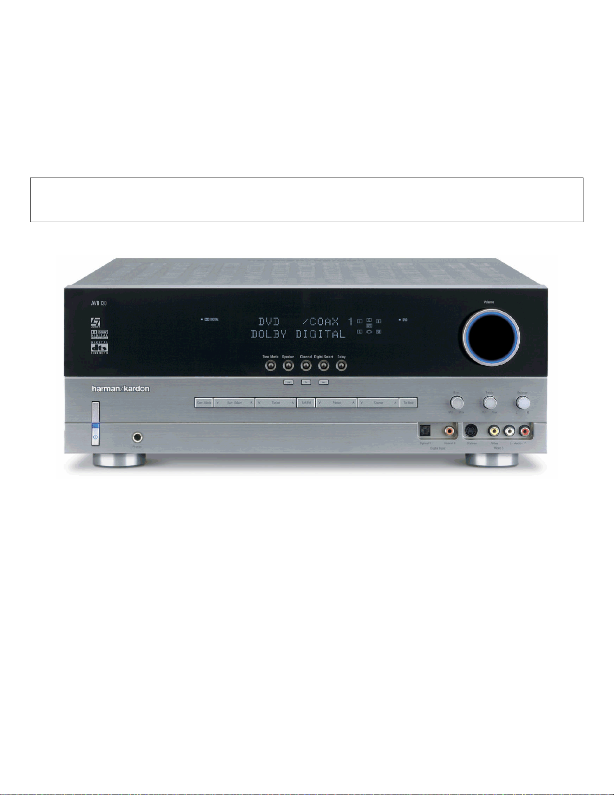
harman/kardon
AVR130
5 X 45W 5.1 CHANNEL A/V RECEIVER
SERVICE MANUAL
ESD WAR N ING……………………………….2
LEAKAGE TESTING……………….…..…....3
BASIC SPECIFICATIONS…………………..4
FRO NT PANEL CO NTRO L S ………..…..…..5
REAR PANEL CONNECTIONS………….…7
REMOTE CONTROL FUNCTIONS.…….….9
TROUBLESHOOTING GUIDE…...……..…13
PROCESSOR RESET……………….….…..13
DISASSEM BLY……………….……...………14
BULLETIN HK 2003-10……………….….…..15
TECH TIP HK2004-03…...….….………..…17
harman/kardon, Inc.
250 Crossways Park Dr.
Woodbury, New York 11797 Rev2 7/2005
CONTENTS
TECH TIP HK2003-01…...….….………….21
UNIT EXPLOD ED VIEW……………….…...22
BLOCK DIAGRAM…….........................….23
AMP BIAS ADJUSTMENT………………...24
PCB DRAWINGS…………………………..25
ELECTRICAL PARTS LIST……………….31
SEMICONDUCTOR PINOUTS……………60
SCHEMATICS………………………………102
WIRING DIAGRAM…………………….…..118
PACKAGING…………………………….….119
Page 2
AVR130 harman/kardon
2
Some semiconductor (solid state) devices can be damaged easily by static electricity. Such components commonly are called
Electrostatically Sensitive (ES) Devices. Examples of typical ES devices are integrated circuits and some field effect transistors and
semiconductor "chip" components.
The following techniques should be used to help reduce the incidence of component damage caused by static electricity.
1. Immediately before handling any semiconductor component or semiconductor-equipped assembly, drain off any electrostatic charge on
your body by touching a known earth ground. Alternatively, obtain and wear a commercially available discharging wrist strap device,
which should be removed for potential shock reasons prior to applying power to the unit under test.
2. After removing an electrical assembly equipped with ES devices, place the assembly on a conductive surface such as aluminum foil, to
prevent electrostatic charge build-up or exposure of the assembly.
3. Use only a grounded-tip soldering iron to solder or unsolder ES devices.
4. Use only an anti-static solder removal device. Some solder removal devices not classified as "anti-static" can generate electrical charges
sufficient to damage ES devices.
5. Do not use freon-propelled chemicals. These can generate electrical change sufficient to damage ES devices.
6. Do not remove a replacement ES device from its protective package until immediately before you are ready to install it. (Most replacement
ES devices are packaged with leads electrically shorted together by conductive foam, aluminum foil or comparable conductive material.)
7. Immediately before removing the protective material from the leads of a replacement ES device, touch the protective material to the
chassis or circuit assembly into which the device will be installed.
CAUTION :
8. Minimize bodily motions when handling unpackaged replacement ES devices. (Otherwise harmless motion such as the brushing together
or your clothes fabric or the lifting of your foot from a carpeted floor can generate static electricity sufficient to damage an ES devices.
Be sure no power is applied to the chassis or circuit, and observe all other safety precautions.
Each precaution in this manual should be followed during servicing.
Components identified with the IEC symbol in the parts list are special significance to safety. When replacing a component identified with
, use only the replacement parts designated, or parts with the same ratings or resistance, wattage, or voltage that are designated in the
parts list in this manual. Leakage-current or resistance measurements must be made to determine that exposed parts are acceptably
insulated from the supply circuit before retuming the product to the customer.
Page 3
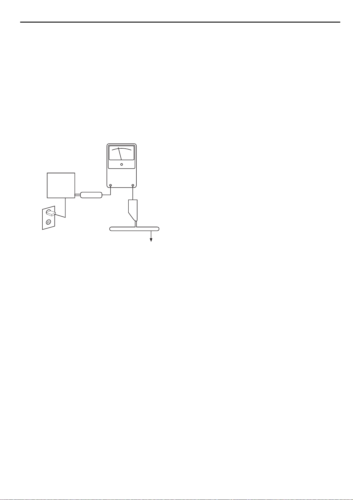
SAFETY PRECAUTIONS
The following check should be performed for the continued
protection of the customer and service technician.
LEAKAGE CURRENT CHECK
Measure leakage current to a known earth ground (water
pipe, conduit, etc.) by connecting a leakage current tester
between the earth ground and all exposed metal parts of the
appliance (input/output terminals, screwheads, metal
overlays, control shaft, etc.). Plug the AC line cord of the
appliance directly into a 120V AC 60Hz outlet and turn the
AC power switch on. Any current measured must not exceed
o.5mA.
ANY MEASUREMENTS NOT WITHIN THE LIMITS
OUTLINED ABOVE ARE INDICATIVE OF A
POTENTIAL SHOCK HAZARD AND MUST BE
CORRECTED BEFORE RETURNING THE APPLIANCE
TO THE CUSTOMER.
AVR130 harman/kardon
3
Reading should
not be above
0.5mA
Device
under
test
Leakage
current
tester
Test all
exposed metal
surfaces
Also test with
plug reversed
(Using AC adapter
plug as required)
Earth
ground
AC Leakage Test
Page 4

AVR 130 TECHNICAL SPECIFICATIONS
Audio Section
Stereo Mode
Continuous Average Power (FTC)
55 Watts per channel,@ < 0.07% THD, 20Hz – 20kHz,
both channels driven into 8 ohms
Five Channel Surround Modes
Power Per Individual Channel
Front L&R channels:
45 Watts per channel
@ < 0.07% THD, 20Hz–20kHz into 8 ohms
Center channel:
45 Watts @ < 0.07% THD,20Hz–20kHz into 8 ohms
Surround channels:
45 Watts per channel
@ < 0.07% THD, 20Hz–20kHz into 8 ohms
Input Sensitivity/Impedance
Linear (High-Level) 200mV/47k ohms
Signal-to-Noise Ratio (IHF-A) 100dB
Surround System Adjacent Channel Separation
Pro Logic II 45dB
Dolby Digital (AC-3) 55dB
DTS 55dB
Frequency Response
@ 1W (+0dB,–3dB) 10Hz– 130kHz
High Instantaneous
Current Capability (HCC) ±25 Amps
Transient Intermodulation
Distortion (TIM) Unmeasurable
Slew Rate 40V/µsec
FM Tuner Section
Frequency Range 87.5 –108.0MHz
Usable Sensitivity IHF 1.3µV/ 13.2dBf
Signal-to-Noise Ratio Mono/Stereo 70dB/68dB
Distortion Mono/Stereo 0.2%/0.3%
Stereo Separation 40dB @ 1kHz
Selectivity ±400kHz, 70dB
Image Rejection 80dB
IF Rejection 90dB
AM Tuner Section
Frequency Range 520 –1720kHz
Signal-to-Noise Ratio 45 dB
Usable Sensitivity Loop 500 µV
Distortion 1kHz, 50% Mod 0.8%
Selectivity ±10kHz, 30dB
Video Section
Television Format NTSC
Input Level/Impedance 1Vp-p /75 ohms
Output Level/Impedance 1Vp-p /75 ohms
Video Frequency
Response 10Hz–8MHz (–3dB)
General
Power Requirement AC 120V/60Hz
Power Consumption 68W idle,540W maximum
(2 channels driven)
Dimensions (Product) (Shipping)
Width 17.3 inches (440mm) 21.5 inches (545mm)
Height 6.6 inches (168mm) 9.9 inches (251mm)
Depth 15 inches (382mm) 17.9 inches (455mm)
(Product) (Shipping)
Weight 23.8 lb (10.8kg) 28.2 lb (12.8kg)
Depth measurement includes knobs,buttons and ter minal connections.
Height measurement includes feet and chassis.
All features and specifications are subject to change without notice.
Harman Kardon, Power for the Digital Revolution and Logic 7 are registered trademarks of
Harman International Industries,Incorporated.
*Manufactured under license from Dolby Laboratories.“Dolby,”“Pro Logic” and the Double-D symbol
are registered trademarks of Dolby Laboratories.Confidential Unpublished Works.
©1992–1999 Dolby Laboratories,Inc.All rights reserved.
“DTS,”“DTS Digital Surround” and “DTS Stereo”are registered trademarks of Digital Theater Systems, Inc.
VMAx is a registered trademark of Harman International Industries,Inc.,and is an
implementation of Cooper Bauck Transaural Stereo under patent license.
Cirrus is a registered trademark of Cirrus Logic Corp.
TiVo is a registered trademark of TiVo Inc.
AVR130 harman/kardon
4
4 TECHNICAL SPECIFICATIONS
Page 5
1 Main Power Switch: Press this button to apply
power to the AVR 130.When the switch is pressed
in, the unit is in a Standby mode, as indicated by the
amber LED
2 above the Standby/On Switch 3.
This button MUST be pressed in to operate the unit.
To turn the unit off and prevent the use of the
remote control, this switch should be pressed until it
pops out from the front panel and the word “OFF”is
seen at the top of the switch.
NOTE: This switch is normally left in the “ON” position.
2 Power Indicator: This LED lights amber when the
unit is in the Standby mode to signal that the AVR is
ready to be turned on.When the unit is
in operation,
the indicator is blue.
3 Standby/On Switch: When the Main Power
Switch
1
is “ON,” press this button to turn on the
AVR 130;press it again to turn the unit off.The
Power Indicator3turns blue when the unit is on.
4 Headphone Jack:This jack may be used to listen
to the AVR 130’s output through a pair of headphones.
The speakers will automatically be turned off when the
headphone jack is in use.
5 Tone Mode Selector Buttons:Pressing this but-
ton enables or disables the Bass and Treble tone controls.When the button is pressed so that
TONE
IN
appears in the Lower Display Line ¯, the
Bass Ó and Treble Ú controls may be used to
adjust the output signals.When the button is pressed
once or twice so that the words
TONE OUT
appear in the Lower Display Line ¯, the output
signal will be “flat,”no matter how the actual
Bass and
TrebleControls ÓÚ are adjusted.
6 Speaker Selector: Press this button to begin the
process of configuring the unit to match the type of
speakers used in your listening room. (See pages
16 –19 for more infor mation on speaker setup and
configuration.)
7 Surround Mode Group Selector: Press this
button to select the top-level group of surround
modes.Each press of the button will select the
current mode in each of the major groupings (e.g.,
Dolby,DTS, Logic 7, DSP, Stereo).
When the button is pressed so that the name of a mode
in the desired surround-mode group appears in the onscreen display and in the
Lower Display Line ¯,
press the
Surround Mode Selector 8 to cycle
through the individual modes available. For example,
press this button to select Dolby modes,and then press
the
Surround Mode Selector 8 to choose from the
various mode options.
FRONT-PANEL CONTROLS
1 Main Power Switch
2 Power Indicator
3 Standby/On Switch
4 Headphone Jack
5 Tone Mode Selector Buttons
6 Speaker Selector
7 Surround Mode Group Selector
8 Surround Mode Selector
9 Tuning Selector
) ‹/› Buttons
! Tuner Band Selector
@ Set Button
# Digital Input Selector
$ Preset Stations Selector
% Delay Adjust Selector
^ Input Source Selector
& Tuner Mode Selector
* Optical 3 Digital Input
( Coaxial 3 Digital Input
Ó Bass Control
Ô Video 3 Video Input Jacks
Video 3 Audio Input Jacks
Ò Balance Control
Ú Treble Control
Û Channel Adjust Selector
Ù Volume Control
ı Input Indicators
ˆ Speaker/Channel Input Indicators
˜ Upper Display Line
¯ Lower Display Line
˘ Surround Mode Indicators
¸ Remote Sensor Window
DIGITAL LOGIC 7
VID 1
DVD
CD
FMAM
TAPE
VID 2
VID 3
PRO LOGIC
3 STEREO DSP
5 CH. STEREO
SURR. OFF
1
2
3
4
6
79
#
^
$
¸
˘
¯˜ ˆ Ú
Ò
Ô
(
*
Û
Ù
ı
5
8
)
!
@
)
&
%
6 CH
Surr. Select
Coaxial 3
Ó
NOTE: To make it easier to follow the instructions that refer to this illustration, a larger copy may be downloaded from the Product Support section for this product
at www.harmankardon.com.
AVR130 harman/kardon
5
5 FRONT-PANEL CONTROLS
Page 6

Û Channel Adjust Selector: Press this button to
begin the process of trimming the channel output levels using an external audio source.(For more information on output level trim adjustment, see page 26.)
Ù Volume Control: Turn this knob clockwise to
increase the volume,counterclockwise to decrease
the volume.If the AVR130 is muted, adjusting the
Volume Control Ù will automatically release
the unit from the silenced condition.
ı Input Indicators: The name of the selected input
will appear here.
ˆ Speaker/Channel Input Indicators: These indi-
cators are multipurpose,indicating both the speaker
type selected for each channel and the incoming datasignal configuration.The left, center,right, right surround
and left surround speaker indicators are composed of
three boxes,while the subwoofer is a single box.The
center box lights when a “small”speaker is selected,
and the two outer boxes light when “large”speakers are
selected.When none of the boxes are lit for the center,
surround or subwoofer channels,no speaker has been
assigned that position. (See page 16 for more information on configuring speakers.) The letters inside each
box display the active input channels.For standard analog inputs,only the L and R will light,indicating a stereo
input. For a digital source,the indicators will light to display the channels being received at the digital input.
When the letters flash, the digital input has been interrupted. (See pages 18–19 for more information on the
Channel Indicators.)
˜ Upper Display Line: Depending on the unit’s sta-
tus,a variety of messages will appear here.In nor mal
operation, this line will show the current input source
and which analog or digital input is in use.When the
tuner is the input, this line will identify the station as AM
or FM and show the frequency and preset number, if
any.
¯ Lower Display Line: Depending on the unit’s sta-
tus,a variety of messages will appear here.In nor mal
operation, the current surround mode will show here.
˘ Surround Mode Indicators: The name of the
selected surround mode will appear here.
¸ Remote Sensor Window: The sensor behind
this window receives infrared signals from the remote
control.Aim the remote at this area and do not block
or cover it.
AVR130 harman/kardon
6
FRONT-PANEL CONTROLS
8 Surround Mode Selector: Press this button
to select from among the available surround mode
options for the mode group selected.The specific
modes will vary based on the number of speakers
available,the mode group and if the input source is
digital or analog.For example,press the
Mode Group Selector
such as Dolby or Logic 7, and then press this button
to see the available mode choices.For more information on mode selection, see pages 22 and 23.
9 Tuning Selector: Press the left side of the button
to tune lower-frequency stations and the right side of
the button to tune higher-frequency stations.When the
tuner is in the MANUAL mode,each tap will increase
or decrease the frequency by one increment.When
the tuner receives a strong enough signal for adequate
reception,
Lower Display Line ¯.When the tuner is in the
AUTO mode,press the button once,and the tuner will
scan for a station with acceptable signal strength.
When the next station with a strong signal is tuned,
the scan will stop and the
will indicate AUTO TUNED.When an FM Stereo
station is tuned, the display will read
TUNED
To switch back and forth between the Auto and
Manual tuning modes,press the
Selector
) ‹/› Buttons: When configuring the AVR 130’s
settings,use these buttons to select from the choices
available,
Lines
! Tuner Band Selector:Press this button to turn
the AVR on and switch to select the Tuner as the input
source.Press it again to switch between the AM and
FM frequency bands.(See page 25 for more information on the tuner.)
@ Set Button: When making choices during the
setup and configuration process,press this button to
enter the desired setting into the AVR130’s memory.
MANUAL TUNED will appear in the
.
&.
as shown in the Upper or Lower Display
˜¯.
7 to select a mode grouping
Lower Display Line ¯
Surround
AUTO ST
Tuner Mode
^ Input Source Selector: Press this button to
change the input by scrolling up or down through the
list of
Input Indicators ı.
& Tuner Mode Selector: Press this button to select
Auto or Manual tuning.When the button is pressed so
that
AUTO appears in the Lower Display Line ¯,
the tuner will search for the next station with an
acceptable signal when the
is pressed.When the button is pressed so that
MANUAL appears in the Lower Display Line ¯,
each press of the
increase the frequency.This button may also be used to
switch between Stereo and Mono modes for FM radio
reception.When weak reception is encountered, press
the button so that
Display Line
again to switch back to STEREO mode.(See page 25
for more information on using the tuner.)
* Optical 3 Digital Input: Connect the optical digital
audio output of an audio or video product to this jack.
When the input is not in use,be certain to keep the
plastic cap installed to avoid dust contamination that
might degrade future performance.
( Coaxial 3 Digital Input: This jack is used for
connection to the output of portable audio devices,
video game consoles or other products that have a
coax digital audio jack.
Ó Bass Control: Turn this control to modify the lowfrequency output of the left/right channels by as much as
±10dB,when the unit is in the “Surround Off” mode.
Ô Video 3 Video Input Jacks: These jacks may be
used for temporary connection to the composite or SVideo output of video games,camcorders or other
portable video products.You may make a connection
to either jack at any time,but not both simultaneously.
Video 3 Audio Input Jacks: These audio jacks
may be used for temporary connection to video
games or portable audio/video products such as camcorders and portable audio players.
¯ to switch to Mono reception.Press it
Tuning Selector 9u
Tuning Selector 9u will
MANUAL appears in the Lower
37
# Digital Input Selector: Press this button to
select one of the digital inputs or the analog input for
any source.(See pages 23–25 for more information
on digital audio.)
$ Preset Stations Selector: Press this button to
scroll up or down through the list of stations that have
been entered into the preset memory.(See page 25
for more information on tuner presets.)
% Delay Adjust Selector: Press this button to
begin the steps required to enter delay settings.(See
page 19 for more information on delay times.)
Ò Balance Control: Turn this control to change the
relative volume for the front left/right channels.
NOTE: For proper operation of the surround modes
this control should be at the midpoint or “12 o’clock”
position.
Ú Treble Control:Turn this control to modify the high
frequency output of the left/right channels by as much as
±10dB,when the unit is in the “Surround Off” mode.
FRONT-PANEL CONTROLS 6
Page 7
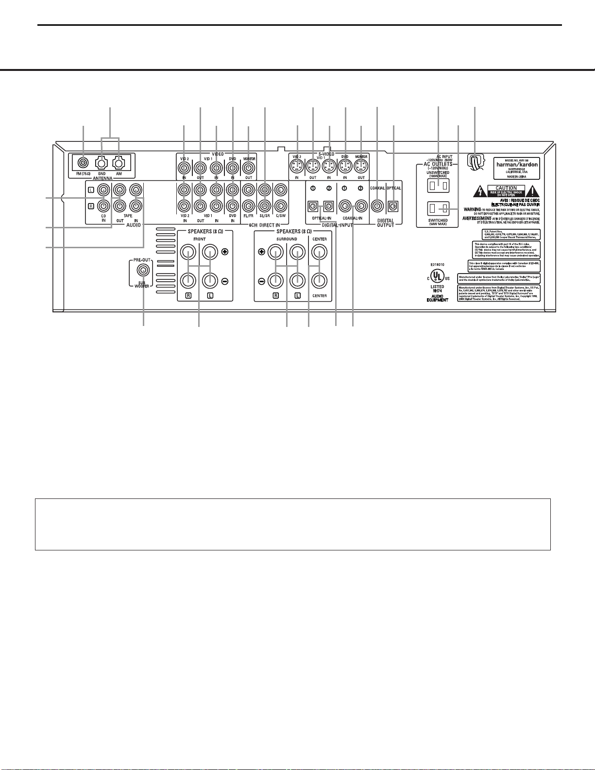
REAR-PANEL CONNECTIONS
•
¢
∞
§
¶
‚
⁄
¤
fi
°
b
c
d
e
g
h
ª
¡
™
£
f
a
·
‡
fl
›
‹
¡ CD Audio Inputs
™ Tape Outputs
£ Tape Inputs
¢ Subwoofer Output
∞ Front Speaker Outputs
§ Surround Speaker Outputs
¶ Center Speaker Outputs
• Optical Digital Inputs
ª Coaxial Digital Inputs
‚ AC Power Cord
⁄ Switched AC Accessory Outlet
¤ Unswitched AC Accessory Outlet
‹ Optical Digital Output
› Coaxial Digital Output
fi S-Video Monitor Output
fl DVD S-Video Input
‡ Video 1 S-Video Input
° Video 1 S-Video Output
· Video 2 S-Video Input
a 6-Channel Direct Inputs
b Video Monitor Output
c DVD Audio/Video Inputs
d Video 1 Audio/Video Inputs
e Video 1 Audio/Video Outputs
f Video 2 Audio/Video Inputs
g AM Antenna T erminals
h FM Antenna Jack
¡ CD Audio Inputs: Connect these jacks to the out-
put of a Compact Disc player or changer.
™ Tape Outputs: Connect these jacks to the
RECORD/INPUT jacks of an audio recorder.
£ Tape Inputs: Connect these jacks to the
PLAY/OUTjacks of an audio recorder.
¢ Subwoofer Output: Connect this jack to the line-
level input of a powered subwoofer. If an external subwoofer amplifier is used, connect this jack to the subwoofer amplifier input.
∞ Front Speaker Outputs: Connect these outputs
to the matching + and – terminals on your front
speakers.
§ Surround Speaker Outputs: Connect these out-
puts to the matching + or – terminals on your left and
right surround speakers.
¶ Center Speaker Outputs: Connect these speak-
er outputs to the matching (+) and (–) terminals on
your center channel speaker.
NOTE ON ALL SPEAKER CONNECTIONS:When
making speaker connections always make certain to
maintain correct polarity by connecting the black terminal to the negative (–) terminal on the speakers.
Connect the blue terminal to the positive (+) terminal
on the left surround speaker and the gray terminal to
the positive (+) terminal on the right surround speaker.
When a newer complete 5-piece speaker system is
used, the individual speakers may have matching color
terminals in accordance with CEA specifications,while
existing speakers typically use a red terminal for the
positive (+) speaker wire connection. (See page 13
for more information on speaker polarity.)
NOTE: To make it easier to follow the instructions that refer to this illustration, a larger copy may be downloaded from the Product Support section for this product at
www.harmankardon.com.
NOTE:To assist in making the correct connections for
multichannel input, output and speaker connections,
all connection jacks and terminals are color-coded
in conformance with the CEA standards as follows:
Front Left: White
Front Right: Red
Center: Green
Surround Left: Blue
Surround Right: Gray
Subwoofer: Purple
Coaxial Digital Audio: Orange
Composite Video: Yellow
AVR130 harman/kardon
7
7 REAR-PANEL CONNECTIONS
Page 8

• Optical Digital Inputs: Connect the optical digital
audio output from a DVD player, HDTV receiver, LD
player, satellite receiver, cable box, MiniDisc player or
recorder, or CD player to these jacks.The signal may
be either a Dolby Digital signal, a DTS signal or a
standard PCM digital source.
ª Coaxial Digital Inputs: Connect the coax digital
audio output from a DVD player, HDTV receiver,LD
player, satellite receiver,cable box, MiniDisc recorder or
CD player to these jacks.The signal may be either a
Dolby Digital signal, DTS signal or a standard PCM digital
source.Do not connect the RF digital output of an
LD player to these jacks.
NOTE: The default setting for the audio input associated
with DVD is the Coaxial Digital Input 1 ª. If you
connect the audio outputs of a DVD player to another
digital or analog audio jack, change the input setting
as shown on page 19.
‚ AC Power Cord: Connect the AC plug to an
unswitched AC wall outlet.
⁄ Switched AC Accessory Outlet: This outlet may
be used to power any device you wish to have turned
on or off at the same time as the AVR 130.Any device
connected to this outlet will be off when the AVR130
is in the Standby mode,and power will be supplied to
the outlet when the AVR130 is turned on.
¤ Unswitched AC Accessory Outlet: This outlet
may be used to power any AC device. The power will
remain on at this outlet regardless of whether the
AVR 130 is on or off.
IMPORTANT NOTE:The total power consumption of
all devices connected to the accessory outlets should
not exceed 100 watts.Do not connect power amplifiers
or other high-current-draw devices to these outlets.
‹ Optical Digital Output: Connect this jack to the
matching digital audio input connector on a digital
recorder such as a CD-R or MiniDisc recorder.
› Coaxial Digital Output: Connect this jack to the
matching digital audio input connector on a digital
recorder such as a CD-R or MiniDisc recorder.
fi S-Video Monitor Output: When your television
or other video display is equipped with an S-Video
input and you are using at least one video source
with S-Video capability,connect this jack to the SVideo input on the video display.
fl DVD S-Video Input: If you are not making a
direct connection from the component video outputs
of your DVD player to a television or other video display,connect the S-Video output of the DVD player to
this jack and then make certain that the
S-Video
Monitor Output
fi is also connected as described
above.
‡ Video 1 S-Video Input: If the product connected
to the
Video 1 Audio Inputs d has S-Video capability,connect this jack to the PLAY/OUT S-Video jack
on that unit and then make cerain that the
S-Video
Monitor Output
fi is also connected as described
above.
° Video 1 S-Video Output: If the product
connected to the
Video 1 Audio Outputs e has
S-Video capability,connect this jack to the REC/IN
S-Video jack on that unit.
· Video 2 S-Video Input: If the product connected
to the
Video 2 Audio Inputs f has S-Video capability,connect this jack to the PLAY/OUT S-Video jack
on that unit and then make certain that the
S-Video
Monitor Output
fi is also connected as described
above.
a 6-Channel Direct Inputs: Connect the outputs of
a DVD Audio or SACD player,or another product with
built-in multichannel decoding,to these jacks.
These jacks have been color-coded as follows to
assist you in making correct channel connections:
Front Left White
Front Right Red
Center Green
Surround Left Blue
Surround Right Gray
Subwoofer Purple
b Video Monitor Output: Connect this jack to the
composite video input of a TV monitor or video
projector to view the output of any standard video
source selected by the receiver’s video switcher.
c DVD Audio/Video Inputs: Connect one of these
jacks to the composite video and L/R analog audio
output jacks on a DVD or other video source.
NOTE: The default setting for the audio input associated
with DVD is the Coaxial Digital Input 1 ª. If you
connect the audio outputs of a DVD player to another
digital or analog audio jack, change the input setting
as shown on page 19.
d Video 1 Audio/Video Inputs: Connect these
jacks to the
PLAY/OUTcomposite video jacks and
L/R audio jacks on a VCR or other video source.
e Video 1 Audio/Video Outputs: Connect these
jacks to the
RECORD/INPUT composite video and
L/R audio jacks on a VCR.
f Video 2 Audio/Video Inputs: Connect these
jacks to the
PLAY/OUTcomposite video and L/R
audio jacks on a TV, VCR or other video source.
g AMAntenna Terminals:Connect the AM loop
antenna supplied with the receiver to these terminals.If
an externalAM antenna is used, make connections to
the
AM and GND terminals in accordance with the
instructions supplied with the antenna.
h FM Antenna Jack: Connect the supplied indoor or
an optional external FM antenna to this jack.
Note on Video Connections:When connecting a
source device such as a VCR,DVD Player,cable or
satellite set top box or video game to the AVR,use
either a composite or S-Video connection for each
input, but not both.
REAR-PANEL CONNECTIONS
AVR130 harman/kardon
8
REAR-PANEL CONNECTIONS 8
Page 9
REMOTE CONTROL FUNCTIONSREMOTE CONTROL FUNCTIONS
●
●
●
●
●
●
●
●
●
●
●
●
●
s
a
bc
d
e
f
g
h
j
n
n
pp
o
q
r
t
v
`
32
30
29
28
36
37
38
39
40
31
z
x
35
POWER
MUTE
AVR
DVD
AM/FM
CD
TAPE
VID 2
VCR
TV
CBL/SAT
6 CH.
VID 1
VID 3
OFF
ON
SLEEP
T/V
SURR.
CH.
VOL.
G
U
I
D
E
C
H
.
E
X
I
T
D
I
G
I
T
A
L
M
E
N
U
S
P
K
R
P
R
E
V
.
C
H
.
D
E
L
A
Y
SET
1
2
3
4
7
6
5
9
0
TUN-M
MEM
M2
M3
M4
D.SKIP
M1
DIRECT
TUNING
DOLBY
DTS SURR
DTS NEO:6
STEREO
LOGIC 7
SKIP
UP
DOWN
PRESET
CLEAR
TEST
NIGHT
130
8
l
u
DIM
i
k
m
34
33
w
y
a Power Off Button
b IR T ransmitter Window
c Program Indicator
d Power On Button
e Input Selectors
f AVR Selector
g AM/FM Tuner Select
h Dim Button
i Test Button
j Sleep Button
k DSP Surround Mode Selector
l Night Mode Button
m Channel Select Button
n
⁄¤
Buttons
o Set Button
p
‹›
Buttons
q Digital Select Button
r Numeric Keys
s Tuner Mode Button
t Direct Button
u Tuning Up/Down Buttons
v Macro Buttons
w Dolby Mode Select Button
x DTS Digital Mode Select Button
y Logic 7 Mode Select Button
z Track Skip Up/Down Buttons
` Transport Controls
28
Stereo Mode Selector Button
29
DTS Neo:6 Mode Select Button
30
Disc Skip Button
31
Preset Up/Down Buttons
32
Clear Button
33
Memory Button
34
Delay Button
35
Speaker Select Button
36
Spare Button
37
Volume Up/Down Button
38
TV/Video Button
39
6-Channel Direct Input Button
40
Mute
NOTES:
• The function names shown here refer to each
button’s feature when used with the AVR 130.
Most buttons have additional functions when
used with other devices.See pages 31–32 for
a list of these functions.
• To make it easier to follow the instructions that
refer to this illustration, a larger copy may be
downloaded from the Product Support section for
this product at www.harmankardon.com.
AVR130 harman/kardon
9
9 REMOTE CONTROL FUNCTIONS
Page 10
NOTE: The Sleep Button j and DSP Surround
Mode Selector
k may also function as the
Channel + and – keys when the remote is programmed for use with TVs, cable boxes,VCRs, satellite
receivers or other video devices with tuners.See page
29 for information on programming the remote for
Channel Control Punch-Through capability so that you
may change channels on a separate device when the
remote is in AVR mode.
l Night Mode Button: Press this button to acti-
vate the Night mode.This mode is available in specially
encoded digital sources to preserve dialogue (center
channel) intelligibility at low volume levels.
m Channel Select Button: This button is used to
start the process of setting the AVR 130’s output levels to
an external source.Once this button is pressed,use the
⁄/¤
Buttons n to select the channel being adjust-
ed, then press the
Set Button o,followed by the
⁄/¤
Buttons n again, to change the level setting.
(See page 26 for more information.)
n
⁄¤
Buttons:These multipurpose buttons are
used to change configuration settings,such as output
levels.When changing an item such as the surround
mode or digital input directly,first press the function or
mode to be changed (e.g., press the
Digital Select
Button
q to change the digital input) and then press
this button to scroll through the list of available choices.
o Set Button: This button is used to enter settings
into the AVR 130’s memory.It is also used in the
setup procedures for delay time,speaker configuration
and channel output level adjustment.
p ‹› Buttons: Thess buttons are not used to
operate or configure the AVR 130’s settings,but they
are used as part of the navigation system for other
devices you may operate with the remote,such as DVD
players,video displays and cable or satellite set top
boxes.(See pages 28 and 30–32 for more information
on using the AVR’s remote with other products.)
q Digital Select Button: Press this button to
assign one of the digital inputs
•ª*( to the
source currently in use.(See page 23 for more information on using digital inputs.)
r Numeric Keys: These buttons serve as a ten-
button numeric keypad to enter tuner preset positions.
They are also used to select channel numbers when
TV has been selected on the remote,or to select track
numbers on a CD,DVD or LD player,depending on
how the remote has been programmed.
AVR130 harman/kardon
10
REMOTE CONTROL FUNCTIONS
IMPORTANT NOTE:The AVR 130’s remote may be
programmed to control up to seven devices,including
the AVR 130.Before using the remote, remember to
press the
Input Selector Button e that corresponds to the unit you wish to operate.In addition, the
AVR 130’s remote is shipped from the factory to operate the AVR 130 and most recent Harman Kardon
products.The remote is also capable of operating a
wide variety of other products using the control codes
that are part of the remote.Before using the remote
with other products,follow the instructions on pages
27–29 to program the proper codes for the products
in your system.
It is also important to remember that many of the buttons on the remote take on different functions,depending on the product selected using the Device Control
Selectors.The descriptions shown here primarily detail
the functions of the remote when it is used to operate
the AVR 130.(See pages 31–32 for information about
alternate functions for the remote’s buttons.)
a Power Off Button: Pressing this button turns off
(places in the Standby mode) the device that was last
selected by pressing one of the
Input Selectors e.
To place the AVR 130 in the Standby mode, first press
the
AVR Selector Button f and then press this
button.
b IR Transmitter Window:Point this window
towards the AVR 130 when pressing buttons on the
remote to make certain that infrared commands are
properly received.
c Program Indicator: This three-color indicator is
used to guide you through the process of programming the remote.(See pages 27–29 for information
on programming the remote.)
d Power On Button: After selecting a device by
pressing one of the
Input Selectors e,press this
button to turn the device on.To turn on the AVR 130,
press the
AVR Selector Button f.
e Input Selectors: Pressing one of these buttons
will perform three actions at the same time.First, if the
AVR 130 is not turned on, this will power up the unit.
Next, it will select the source shown on the button as
the input to the AVR130. Finally,it will change the
remote control so that it controls the device selected.
After pressing one of these buttons you must press
the
AVR Selector Button f again to operate the
AVR 130’s functions with the remote.
f AVR Selector: Pressing this button will switch the
remote so that it will operate the AVR130’s functions.If
the AVR130 is in the Standby mode, it will also turn the
AVR 130 on.
g AM/FM Tuner Select: Press this button to select
the AVR130’s tuner as the listening choice. Pressing
this button when the tuner is already in use will switch
between the AM and FM bands.
h Dim Button: Press this button to activate the
Dimmer function, which reduces the brightness of the
front-panel display,or tur ns it off entirely.The first
press of the button shows the default state,which is
full brightness,by indicating
the
Lower Display Line ¯. Press the button again
DIMMER FULL in
within five seconds to reduce the brightness by 50%,
as indicated by
DIMMER HALF showing in the
Lower Display Line ¯. Press the button again
within five seconds and the main display will go completely dark. Note that this setting is temporar y,in that,
regardless of any changes,the display will always
return to full brightness when the AVR is turned on.In
addition, both the
Power Indicator 2 and the blue
accent lighting inside the volume control will always
remain at full brightness regardless of the setting.This
is to remind you that the AVR is still turned on.
i Test Button: Press this button to begin the
sequence used to calibrate the AVR 130’s output levels.
(See pages 18–19 for more information on calibrating
the AVR 130.)
j Sleep Button: Press this button to place the unit
in the Sleep mode.After the time shown in the display,
the AVR 130 will automatically go into the Standby
mode.Each press of the button changes the time until
turn-off in the following order:
90
min80min70min60min50min
30
40
min20min10min
min
OFF
Note that when the Sleep function is in use,the display will dim to half brightness.This button is also
used to change channels on your TV when the TV is
selected, and it is also used to end the process of
creating a macro command. (See page 28 for more
information on creating macros.)
k DSP Surround Mode Selector: Press this but-
ton to select one of the DSP surround modes,such as
VMAx, Hall or Theater.Each press of the button
selects another mode.(See page 22 for more information on surround modes.)
REMOTE CONTROL FUNCTIONS 10
Page 11

REMOTE CONTROL FUNCTIONS
s Tuner Mode Button: Press this button to change
the tuner mode between manual and automatic.When
the button is pressed so that
AUTO appears at the
left side of the
Lower Display Line ¯, only stations
with acceptable signal quality will be tuned, and the
tuner will play FM stations in stereo,when available.In
the
AUTO mode,when the TuningUp/Down
Buttons
9u are pressed, the unit will automatically search for the next available station with good
signal strength.When this button is pressed so that
MANUAL appears on the left side of the Lower
Display Line
¯ each press of the Tuning
Up/Down Buttons
9u will move the frequency
up or down in single-step increments.When the FM
band is in use,pressing this button so that the
MANUAL mode is activated will enable you to tune
stations with weak signals by changing to monaural
reception. (See page 25 for more information.)
t Direct Button: When the tuner is in use, press
this button to start the sequence for direct entry of a
station’s frequency. After pressing the button simply
press the proper
Numeric Keys r to select a sta-
tion. (See page 25 for more information on the tuner.)
u Tuning Up/Down Buttons:When the tuner is in
use,these buttons will tune up or down through the
selected frequency band. If the
Tuner Mode Button
s& has been pressed so that the word AUTO
appears in the Lower Display Line ¯,pressing
either of the buttons will cause the tuner to seek the
next station with acceptable signal strength for quality
reception.When the word
MANUAL appears in the
Lower Display Line ¯,pressing these buttons will
tune stations in single-step increments.(See page 25
for more information.)
v Macro Buttons: Press these buttons to store or
recall a “Macro”, which is a preprogrammed sequence
of commands stored in the remote.(See page 28 for
more information on storing and recalling macros.)
w Dolby Mode Select Button: This button is used
to select from among the available Dolby Surround
processing modes.Each press of this button will select
one of the Dolby Pro Logic II modes or Dolby 3
Stereo.When a Dolby Digital-encoded source is in use,
the Dolby Digital mode may also be selected. (See
page 22 for the available Dolby surround mode
options.)
x DTS Digital Mode Select Button: Although
the AVR 130 will automatically select DTS processing
when the digital audio input source is a DTS data
stream, you may also press this button to select
DTS playback.
y Logic 7 Mode Select Button: Press this button
to seelct from among the available Logic 7 surround
modes.(See page 22 for available Logic 7 options.)
z Track Skip Up/Down Buttons:These buttons
have no direct function with the AVR130, but when
used with a compatibly programmed CD or DVD
changer, they will change the track or chapter of the
disc currently being played in the changer.
` Transport Controls:These buttons do not have
any functions for the AVR130, but they may be programmed for the forward/ reverse play operation of a
wide variety of CD or DVD players,and audio or video
cassette recorders.(See page 29 for more information
on programming the Transport Control Punch-Through
capability of the remote.)
Stereo Mode Select Button: Press this button
to select a stereo playback mode.When the button is
pressed so that
DSP SURR OFF appears in the
Lower Display Line ¯, the AVR will operate in a
bypass mode with true fully analog,two-channel
left/right stereo mode with no surround processing or
bass management as opposed to other modes where
digital processing is used.When the button is pressed
so that
SURROUND OFF appears in the Lower
Display Line
¯, you may enjoy a two-channel presentation of the sound along with the benefits of bass
management.When the button is pressed so that
5
CH STEREO
appears,the stereo signal is routed
to all five speakers,if installed. (See page 22 for more
information on stereo playback modes.)
DTS Neo:6 Mode Select Button: Press this
button to select a DTS Neo:6 mode.These modes
take a two-channel stereo- or matrix surroundencoded source and create a full five-channel sound
field. (See page 22 for the available DTS Neo:6
options.)
Disc Skip Button:This button has no direct
function for the AVR 130,but when used with a compatibly programmed CD or DVD changer, it will change
the disc currently being played in the changer. (See
page 28 for more information on using the remote
with other devices.)
Preset Up/Down Buttons: When the tuner is in
use,press these buttons to scroll through the stations
programmed into the AVR 130’s memory.When some
source devices,such as CD players,VCRs and cassette decks,are selected using the device
Input
Selectors
e, these buttons may function as
Chapter Step or Track Advance.
Clear Button: Press this button to clear incorrect
entries when using the remote to directly enter a radio
station’s frequency.
Memory Button: Press this button to enter a radio
station into the AVR 130’s preset memory.First, tune the
desired station, and then press this button. When two
underline indicators flash at the right side of the
Upper
Display Line
˜,press the numeric keys for the preset number between 01 and 30 that you wish to
assign to the station within five seconds.(See page 25
for more information.)
Delay Button: Press this button to begin
the process for setting the delay times used by the
AVR 130 when processing surround sound. After
pressing this button, the delay times are entered by
pressing the
Set Button o and then using the
⁄/¤
Buttons n to change the setting.Press
the
Set Button o again to complete the process.
(See page 19 for more information.)
Speaker Select Button: Press this button to
begin the process of configuring the AVR 130’s bass
management system for use with the type of speakers used in your system. Once the button has been
pressed, use the
⁄/¤
Buttons n to select the
channel you wish to set up.Press the
Set Button
o and then select another channel to configure.
When all adjustments have been completed, press
the
Set Button o twice to exit the settings and
return to normal operation. (See page 16 for more
information.)
Spare Button:This button does not have any
function for the operation of the AVR130, but it is
available for use when programmed with the code
from another remote.(See page 27 for information
on programming the remote with codes for other
devices.)
Volume Up/Down: Press these buttons to raise
or lower the system volume.(See page 29 for more
information on programming the Volume PunchThrough capability of the remote,which allows you to
change the AVR130’s volume while the remote is set
to control another device.)
TV/Video Selector: This button does not have a
direct function on the AVR130, but when used with a
compatibly programmed VCR,DVD or satellite receiver
that has a “TV/Video”function, pressing this button will
switch between the output of the player or receiver
and the external video input to that player. Consult the
owner’s manual for your specific player or receiver for
the details of how it implements this function.
AVR130 harman/kardon
11
28
29
30
31
32
33
34
35
36
37
38
11 REMOTE CONTROL FUNCTIONS
Page 12

AVR130 harman/kardon
12
REMOTE CONTROL FUNCTIONS
39
6-Channel Direct Input: Press this button to
select the component connected to the
Direct Input
you wish to use the 6-Channel Direct Input in conjunction with a video source,you must first select the video
source by pressing one of the
Then press this button to choose the
Direct Input
40
the AVR 130 or TV set being controlled, depending on
which device has been selected.When the AVR 130
is muted, press this button or use the
Control
level.When the AVR 130 remote is being programmed
to operate another device or when a macro command
is being programmed, this button is pressed with the
Input Selector Button e to begin the programming process.(See page 27 for more information on
programming the remote.)
a as the audio source.Note that when
a as the audio source.
Mute: Press this button to momentarily silence
Ù to return to the previous volume
37
6-Channel
Input Selectors e.
6-Channel
Volume
REMOTE CONTROL FUNCTIONS 12
Page 13

AVR130 harman/kardon
13
TROUBLESHOOTING GUIDE
Your AVR 130 receiver has been designed to provide many years of trouble-free service.In the event that you are experiencing difficulties,please check the suggestions
below for a possible solution to your problem.Additional information on the AVR 130,including updated information and user hints, is available from our Web site at
www.harmankardon.com.
SYMPTOM CAUSE SOLUTION
Unit does not function when Main • No AC Power • Make certain AC Power Cord ‚ is plugged into a live outlet
Power Switch 1 is pushed • Check to see whether outlet is switch-controlled
Display lights,but no sound • Intermittent input connections • Make certain that all input and speaker connections
or picture are secure
•
Mute is on • Press Mute Button
• Volume control is down • Tur n up volume control
40
No sound from any speakers • Amplifier is in protection mode • Unplug the
due to possible short connections for shorts at receiver and speaker ends
• Amplifier is in protection mode • Contact your local Harman Kardon service center,which you can
due to internal problems locate by visiting our Web site at www.harmankardon.com
No sound from surround or • Incorrect surround mode • Select a mode other than Stereo or Dolby 3 Stereo
center speakers • Input is monaural • There is no surround information from mono sources
• Incorrect speaker configuration • Check speaker mode configuratioin
• Stereo or Mono program material • The surround decoder may not create center- or rear-channel
information from nonencoded programs
Unit does not respond to • Weak batteries in remote • Change remote batteries
remote commands • Wrong device selected • Press the
• Remote sensor is obscured • Make certain front-panel sensor is visible to remote
Intermittent buzzing in tuner • Local interference • Move unit or antenna away from computers,fluorescent
lights,motors or other electrical appliances
Letters flash in the channel indicator • Digital audio feed paused • Resume play for DVD
display and digital audio stops • Check that appropriate Digital Input is selected
Processor Reset
In the rare case where the unit’s operation or the
displays seem abnormal, the cause may involve the
erratic operation of the system’s memory or microprocessor.
To correct this problem, first unplug the unit from the
AC wall outlet and wait at least three minutes. After
the pause,reconnect the AC power cord and check
the unit’s operation.If the system still malfunctions,a
system “reset”may clear the problem.
press and hold the
seconds.
The unit will reset and then turn on automatically.Once
you have cleared the memory in this manner,it is necessary to reestablish all system configuration settings
and tuner presets.
The reset will not affect settings that were programmed
into the remote control.To reset the remote control
and restore it to the factory default settings,please
follow the instructions on page 29.
Tone Mode Button6 for three
AC Power Cord ‚ and check speaker wire
AVR Selector f
Memory Backup
This product is equipped with a memory backup system that preserves the system configuration information and tuner presets if the unit is accidentally
unplugged or subjected to a power outage.This memory will last for approximately four weeks,after which
time all information must be reentered.
To clear the AVR 130’s entire system memory including the tuner presets,output level settings,delay times
and speaker configuration data, first put the unit in
Standby by pressing the
so that the Power Indicator 2 turns amber.Next,
Standby/On Switch 3
TROUBLESHOOTING GUIDE 13
If these steps do not solve the problem, consult an
authorized Harman Kardon service center.You can
locate the service center nearest to you by visiting our
Web site at www.harmankardon.com.
Page 14
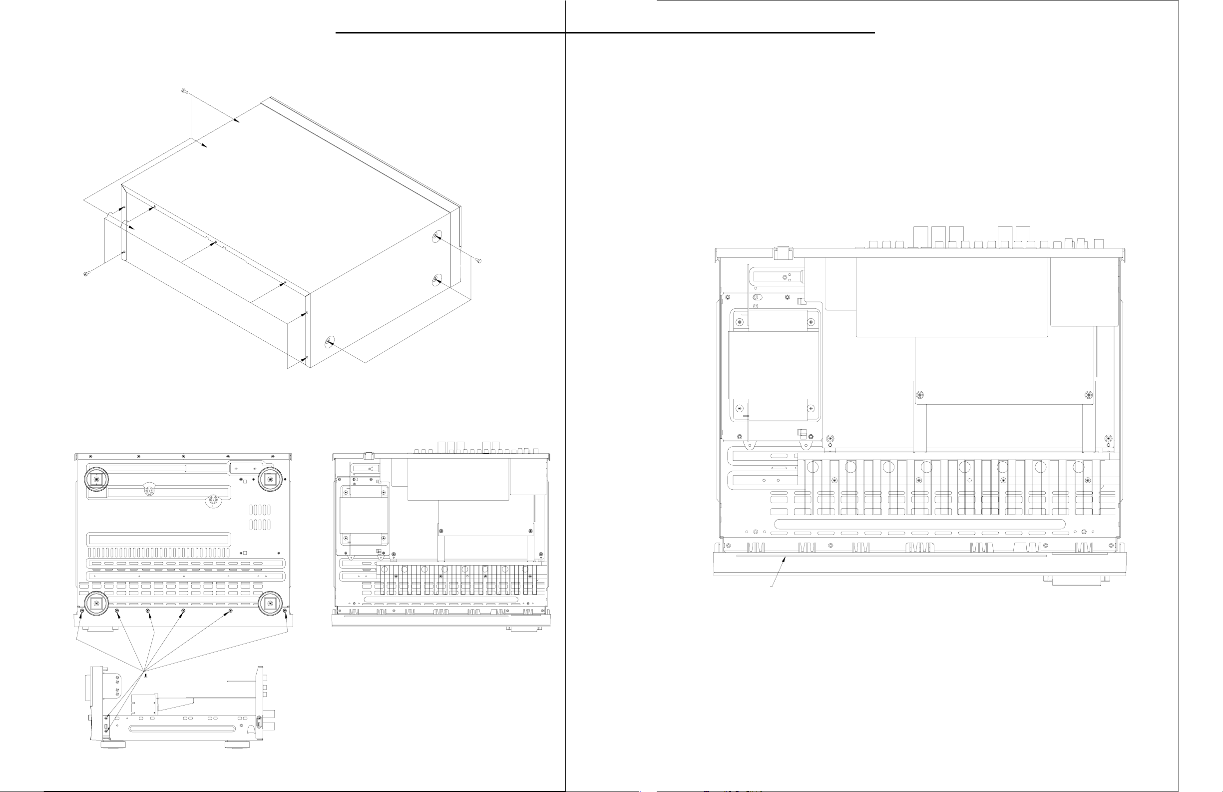
DISASSEMBLY
14
1) REMOVAL OF TOP COVER
AVR130 harman/kardon
3) PRINCIPAL PARTS LOACTION
TUNER
MODULE
VIDEO PCB
2) REMOVAL OF FRONT PANEL
TRANS FORMER
FRONT PCB
INPUT PCB
MAIN PCB
Page 15
15
AVR130 harman/kardon
harman/kardon
Service bulletin # H/K2003-10 December 2003
To: All harman/kardon Service Centers
Models: AVR130, AVR230, AVR330, HK3380, HK3480
Subject: Volume Level Changes
On early versions of the AVR130,AVR230,AVR330,HK3380,HK3480, when the volume control is turned, the
volume level and display may be erratic, and not track accurately, or the level may progress in an unintended
direction. This may happen on a random basis and depends on where the volume control knob is positioned
after a volume adjustment. During a running production change, new volume encoders were installed.
In the event you receive an AVR model listed above with the complaint “The volume control on my
receiver does not track accurately when turned”, perform the following procedure:
REPLACE VR74 (AVR130/230/330) or VR81 (HK3380/3480) VOLUME ENCODER
Note: It is important that the various screws do not get mix ed up and inserted in other locations upon reassembly. Make
note or label eac h r emoved screw set; keep them apart from other screw sets.
1) Remove the top cover, (13) Phillips screws.
2) Remove the volume, bass, treble and balance knobs by pulling them straight out and off. If a tool is
necessary for removal of the smaller knobs, make sure the jaws are insulated to avoid knob damage.
3) Remove the (10) Phillips screws holding the front panel ass’y to the chassis: (6) at the bottom and (4) at
the sides.
4) Cut all plastic cable ties that would prevent you detaching the front panel ass’y from the chassis. Draw a
diagram if necessary, for a location reminder, to aid reassembly.
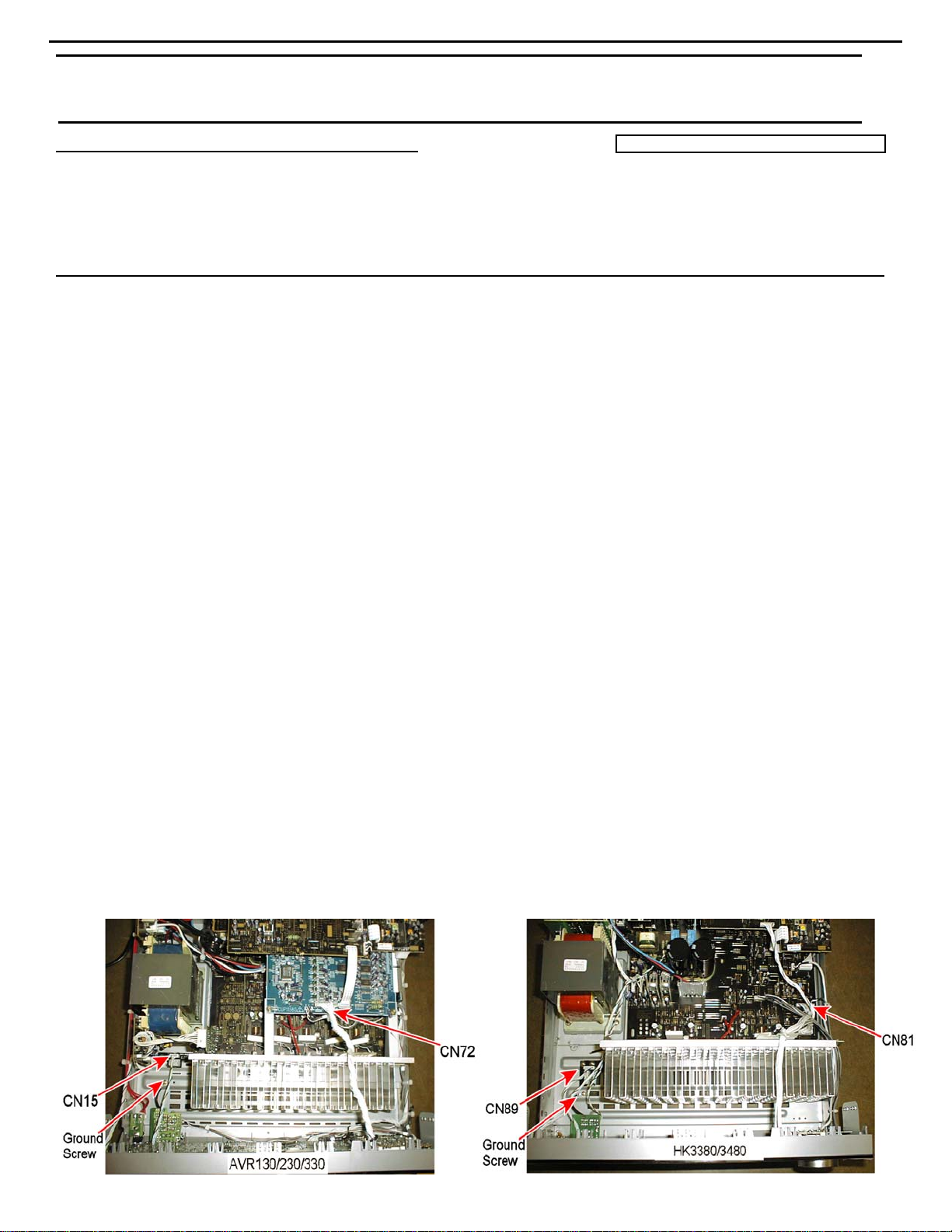
5) Unplug connector CN15 (6 cond) or CN89 (7 cond) at the left side of the unit. See below.
6) Remove single ground screw at the left side of the unit, near CN15 or CN89. (Black wire)
7) Unplug connector CN72 (32 cond) or CN81 (20 cond) on the DSP PCB, coming from the top of the front
panel ass’y. See below.
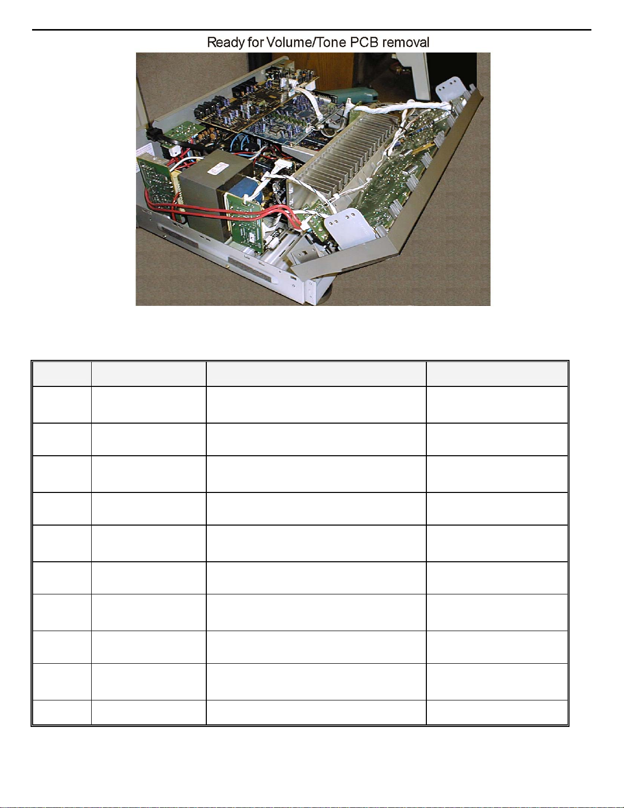
8) There should now be enough slack in the connecting cables to lift and detach the front panel ass’y from
the chassis. Pull the front panel as far away as the remaining connecting wires will allow, enough to tilt
and gain access to the rear of the Tone/Volume PCB. See illustrat ion Page 2.
9) Remove the (10) screws or (9) screws holding the Tone/Volume PCB to the front panel.
10) Detach and pull back the PCB; unplug top connector CN84 (7 cond) or CN83 (4 cond) if necessary.
11) Remove and replace VR74 or VR81 (5 soldered pads) with hk part# HSR2A029Z.
12) Reassemble in reverse order, taking care to replace all connectors, cable ties, and ground screw.
13) Power up receiver, and test volume control to assure setting no longer changes settings by itself, or when
the volume knob is tapped.
Warranty labor rate: MAJOR repair
Service Bulletin
Page 16
16
AVR130 harman/kardon
Model
AVR130
AVR130
AVR230
AVR230
AVR330
AVR330
HK3380
HK3380
HK3480
HK3480
Serial Number
120V
AN0006-01000
to
AN0006-13800
AN0006-13801
and above
AN0007-01000
to
AN0007-11400
AN0007-11401
and above
AN0008-01000
to
AN0008-08524
AN0008-08525
and above
AN0015-01000
to
AN0015-02728
AN0015-02729
and above
AN0016-01000
to
AN0016-01864
AN0016-01865
and above
STATUS ACTION
Volume control may not track accurately when
turned; erratic operation
Modified By Factory NONE REQUIRED
Volume control may not track accurately when
turned; erratic operation
Modified By Factory NONE REQUIRED
Volume control may not track accurately when
turned; erratic operation
Modified By Factory NONE REQUIRED
Volume control may not track accurately when
turned; erratic operation
Modified By Factory NONE REQUIRED
Volume control may not track accurately when
turned; erratic operation
Modified By Factory NONE REQUIRED
Change VR74
Rotary encoder
Change VR74
Rotary encoder
Change VR74
Rotary encoder
Change VR81
Rotary encoder
Change VR81
Rotary encoder
Page 17
17
AVR130 harman/kardon
harman/kardon TECH TIPS
Troubleshooting tips and solutions to common service problems
TIP# HKTT2004-03
Isolating audio problems in an AVR receiver
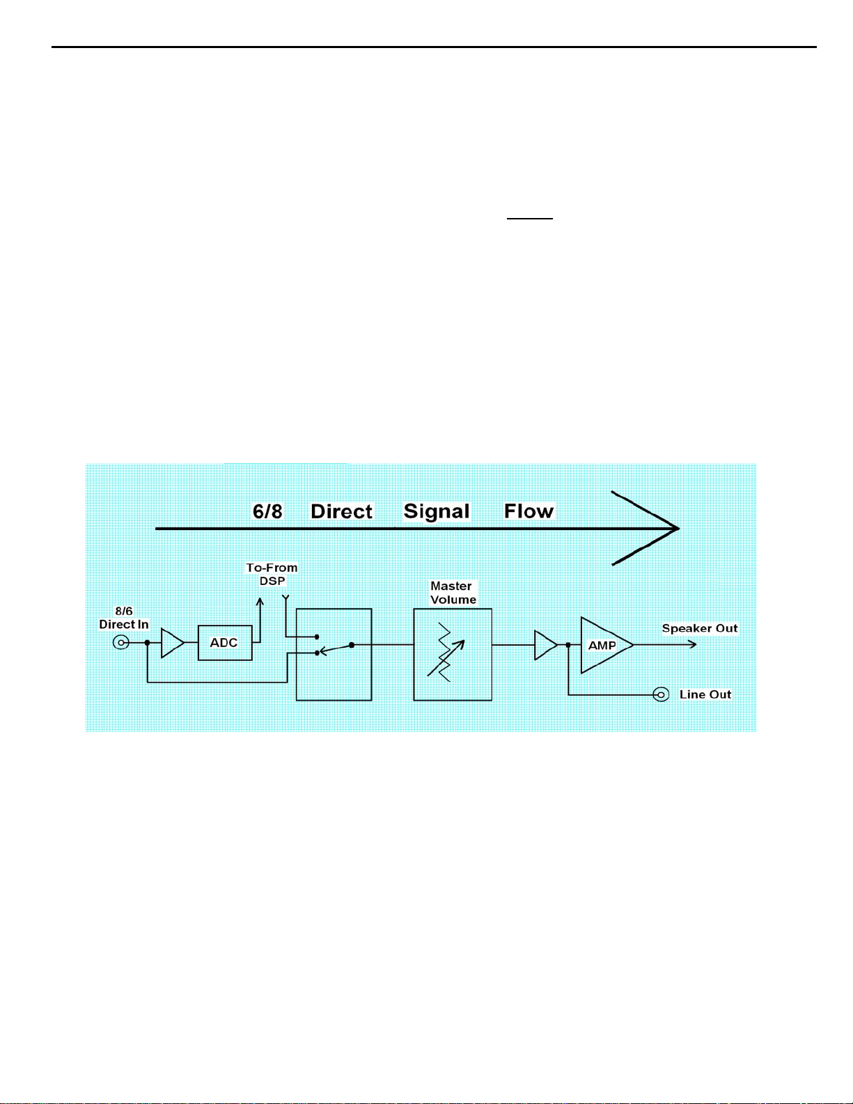
Using 6/8 Direct In
The following charts are used to help the tech quickly isolate
audio problems in an AVR receiver. Use the following
procedures to help find what is working, then to quickly locate
the problem area.
Equipment needed:
9 1 set of (RCA) Y adaptors.
9 Function/signal generator.
9 Oscilloscope.
Procedure:
1) Do a factory reset of the receiver. (This will eliminate any common micro processor
problems.) Reset List can be found in this service manual.
2) Print the block diagram from the service manual.
3) With no inputs or speakers attached to the AVR turn on the receiver and turn the
volume all the way down.
4) Turn unit off.
5) Hook up an oscillator to the 6/8 Direct in jacks using the Y adaptors. Adjust the
oscillator to about 0db (.775Volts RMS).
6) Hook up an oscilloscope to monitor the line out jacks. Or, if there are no line out
(preamp out) jacks monitor the input to the power amps or the speaker outs.
(AVR125, 225, 130 do not have preamp out jacks)
7) Turn the AVR on. Select 6 or 8 direct in, depending on the receiver.
8) Slowly turn the volume control up until you can easily measure the voltage at the line
out jacks. ( -40 to -25db )
Models covered:
AVR210 AVR310
AVR220 AVR320
AVR520 AVR225
AVR125 AVR525
AVR130 AVR230
AVR330 AVR430
AVR630
Harman Consumer Group 250 Crossways Park Dr. Woodbury, New York 11797
Email Techsupport@harman.com
Page 18
18
AVR130 harman/kardon
Isolating audio problems in an AVR receiver
Using 6/8 Direct In
9) At this point you will be able to check and assure all output levels are the same.
10) IF THE OUTPUT LEVELS ARE NOT THE SAME
you will need to use the charts to see where you are losing your signal. The chart
shows the analog signal flow from the input jacks to the output jacks.
11) If the output levels are the same check the power out stage at the speaker out jacks.
12) If you find the levels at the speaker out jacks are OK, your problem will be in the DSP
part of the receiver.
Congratulations! You have now eliminated 90% of the electronics in the AVR and
confirmed that the problem is in the DSP section.
STOP! Go no further. At this point
Harman Consumer Group 250 Crossways Park Dr. Woodbury, New York 11797
Email Techsupport@harman.com
Page 19
19
AVR130 harman/kardon
Isolating audio problems in an AVR receiver
Using 6/8 Direct In
AVR,210,310,510
t
u
n
I
N
I
CH
6
FR 3 1 15 2 4 8 9 4 3 19 17 3 1 3
FL 5 7 13 27 25 21 20 25 26 10 12 5 7 1
SR 11 5 7 7 6 5 7 9
SL 9 24 22 22 23 3 1 7
C 5 21 19 19 20 3 1 5
SW 7 8 10 10 9 5 7 11
I
O
1
1
0
5
C
08
0
4
5
N
C
I
C
C
I
t
u
n
I
O
4
4
0
0
7
C7
C7
I
I
t
u
n
I
O
5
5
0
0
C7
C7
I
I
t
u
O
n
I
6
6
0
0
7
C
C
I
I
AVR220
t
u
n
O
I
N
I
CH
6
FR 5 7 15 2 4 8 9 4 3 5 7 10 12 5 7 1
FL 3 1 13 27 25 21 20 25 26 3 1 19 17 3 1 3
SR 11 5 7 7 6 5 7 9
SL 9 24 22 22 23 3 1 7
C 5 21 19 19 20 3 1 5
SW 7 8 10 10 9 5 7 11
1
0
5
C
I
8
1
0
0
4
5
C
C
CN
I
I
t
u
n
I
O
4
4
0
0
7
C7
C7
I
I
t
u
n
I
O
5
5
0
0
C7
C7
I
I
t
u
O
n
I
6
6
0
0
7
C
C7
I
I
t
u
n
O
I
5
5
0
0
7
1
7
7
C
C
I
I
t
u
n
I
O
4
4
1
7
C
C7
I
I
t
u
n
I
O
6
6
1
1
7
C7
C
I
I
t
u
n
O
I
5
5
0
0
7
7
C
C
I
I
t
u
n
I
O
7
7
1
6
1
1
1
7
7
C
C
I
I
t
u
n
I
O
6
1
1
7
C7
C
I
I
t
u
n
I
O
8
I
n
I
7
I
5
8
0
1
4
7
P
C
C
t
u
O
7
1
7
7
C
C
I
t
u
n
I
O
8
1
I
5
8
0
1
4
7
C
CP
AVR320/520
t
u
n
O
I
C
I
CN4
1
0
5
8
1
C
I
CP
8
1
0
0
4
5
C
CN
I
n
I
2
1
0
0
1
C1
C1
I
I
N
I
CH
8
FR 5 7 15 2 4 8 9 4 3 5 7 10 12 5 7 1
FL 3 1 13 27 25 21 20 25 26 3 1 19 17 3 1 3
SR 11 5 7 7 6 5 7 9
SL 9 24 22 22 23 3 1 7
C 5 21 19 19 20 3 1 5
SW 7 8 10 10 9 5 7 11
SBR 3 3 3 4 21 23 5 7
SBL 1 1 25 26 4 2 3 1
t
u
n
I
O
4
4
0
0
7
C7
C7
I
I
t
u
n
I
O
1
2
0
0
1
C1
c
i
I
t
u
n
I
O
5
5
0
0
C7
C7
I
I
UT
N
i
o
2
3
0
0
1
1
c
c
i
i
t
u
O
n
I
6
6
0
0
7
C
C7
I
I
t
u
O
3
0
t
u
n
I
O
4
4
1
1
7
C
C7
I
I
t
u
n
O
I
5
5
0
0
7
C
C
I
I
t
u
n
I
O
6
6
1
1
7
7
C7
C
I
I
t
u
n
I
7
1
C
I
n
O
I
7
1
7
C
I
O
8
8
1
1
7
7
C
I
AVR225/125
t
t
u
u
N
I
CH
6
L ch 27 25 19 20 5 7 1 3 1 9 10 1 2
R ch 24 22 22 23 3 1 3 5 7 15 14 4 5
SL 5476 579
SR 2 4 10 9 3 1 11
C 81843 31 7
SW 21 19 25 26 5 7 5
n
I
0
3
C
I
n
O
I
0
3
C
I
O
1
1
3
3
C
C
C
I
I
I
t
u
n
I
O
2
2
3
3
C
C
I
I
t
u
n
I
O
3
3
3
3
C
C
I
I
t
u
n
O
I
4
3
2
4
3
N1
C
I
C
I
B
t
u
n
O
I
1
1
8
8
C
C
I
I
t
u
n
I
O
0
0
8
8
N1
C
I
B
t
u
n
O
I
6
6
N1
B
t
u
5
0
4
CP
Harman Consumer Group 250 Crossways Park Dr. Woodbury, New York 11797
Email techsupport@harman.com
Page 20
20
AVR130 harman/kardon
Isolating audio problems in an AVR receiver
Using 6/8 Direct In
AVR 525
t
t
k
c
a
J
n
I
FL 11 109 423 135 3 1 1 1
FR 3 3 21 22 21 23 5 7 28 6 6 7 3 3
SL 5524 43 3 1 5 5
SR 7 7 29 27 25 26 5 7 7 7
CTR 9957 76 3 1 9 9
SW 11 11 26 24 22 23 5 7 11 11
SBL 13 13 8 10 10 9 3 1 13 13
SBR 15 15 23 21 19 20 6 7 15 15
4
0
6
N4
P
u
n
I
O
C5
C5
I
I
t
u
n
O
I
C3
C3
I
I
u
n
n
O
I
9
C1
I
I
8
9
C1
C1
I
C2
I
I
t
u
n
I
O
0
n
I
0
C3
C2
I
C3
I
I
t
u
t
u
O
O
8
C2
C1
I
I
t
u
n
I
O
3
3
C2
C2
I
I
AVR130
t
n
i
h
c
6
L18172123 1
R191242 14
SL 24 22 21 23 9
SR 57 42 7
C27252123 5
SUB 2 4 4 2 3
SBL 21 19 21 23 5 7 13
SBR 8 10 4 2 3 1 11
n
I
3
2
C
I
I
n
I
u
u
O
O
6
3
2
C
2
6
2
C
I
C
I
t
t
n
u
I
O
2
4
2
C
I
I
C4
I
t
n
I
u
O
4
4
4
4
C
I
C
I
t
n
I
u
O
3
4
3
4
C
C
I
t
n
u
I
O
0
4
0
C
I
C4
I
t
n
I
9
4
C
I
C4
I
2
u
O
9
1
1
N1
N
B
B
t
u
n
O
I
5
5
C2
C2
I
I
t
u
n
I
O
4
4
C2
C2
I
I
t
u
n
I
O
6
6
C2
I
6
0
9
P
N8
AVR230/330
t
n
i
h
c
6
L18172123 1
R191242 14
SL 24 22 21 23 9
SR 57 42 7
C27252123 5
SUB 2 4 4 2 3
SBL 21 19 21 23 5 7 13
SBR 8 10 4 2 3 1 11
n
I
3
2
C
I
I
n
I
u
u
O
O
6
3
2
C
2
6
2
C
I
C
I
t
t
n
u
I
O
2
4
2
C
I
I
C4
I
t
n
I
u
O
4
4
4
4
C
I
C
I
t
n
I
u
O
3
4
3
4
C
C
I
t
n
u
I
O
0
4
0
C
I
C4
I
t
n
I
9
4
C
I
C4
I
2
u
O
9
1
1
N1
N
B
B
AVR630/430
t
n
I
CH
8
FL 11012109316931423131
FR 319171920 5 723 20 5 7 2123 5 7 26 7
SL 52443 31
SR 727252526 5 7
CTR 95776 3 1
SW 11 24 22 22 23 5 7
SBL 13 8 10 10 9 3 1
SBR 15 21 19 19 20 5 7
4
0
N4
4
0
N4
u
O
3
3
C
C
I
I
I
t
u
n
I
O
5
5
C
C
I
I
I
t
u
n
I
O
4
4
1
1
C
C
C
I
I
t
u
n
O
I
9
9
1
C1
C
C
I
I
t
t
u
n
O
I
2
2
1
1
C
I
n
O
I
5
5
2
2
C
I
u
n
I
O
3
3
C
I
t
u
C
I
C
C
I
I
t
u
n
I
O
4
4
2
2
C
C
I
I
t
u
n
I
O
7
7
2
2
C
C
I
I
t
u
n
O
I
6
6
2
2
C
I
t
u
n
O
I
8
8
1
1
C
C
I
I
t
u
n
I
O
0
0
2
2
C
C
I
I
t
u
n
I
O
3
3
C
I
Harman Consumer Group 250 Crossways Park Dr. Woodbury, New York 11797
Email techsupport@harman.com
Page 21
21
AVR130 harman/kardon
harman/kardon TECH TIPS
Troubleshooting tips and solutions to common service problems
For models:
AVR7000/7200/7300/8000
AVR100/200/300/500
AVR110/210/310/510
AVR120/220/320/520
AVR125/225/325/525
AVR130/230/330/430/630
AVR135/235/335/435/635
AVR10
DPR1001
DPR1005
DPR2005
HK3370/3470/3375/3475
HK3250
Subject: Backup Memory on AVR/DPR/HK series receivers
In the event of the complaint: “the receiver is losing its memory (any programmed system settings)
when the unit is turned off, or after the unit is unplugged (briefly*)”:
Check and replace:
Model Designator Location Description Part number
AVR10
AVR7000 C730 Front PCB 0.047 Farad 5.5v capacitor
AVR7200 C106 Front PCB 0.047 Farad 5.5v capacitor # P10790-ND
AVR7300 C657 DSP PCB 0.047 Farad 5.5v capacitor # H01-CEZXA0479MN-5
AVR8000 C726 Front PCB 0.047 Farad 5.5v capacitor
AVR100/200 C412 Front PCB 0.047 Farad 5.5v capacitor # CEGT-B473J-0J0
AVR300 C906 Front PCB 0.1Farad 5.5v capacitor
AVR500 C906 Front PCB 0.1Farad 5.5v capacitor
AVR110/210/310/510
AVR120/220/320/520
AVR125/225 C734,C885 Front PCB two 0.1F capacitors in parallel # BCESOHD104
AVR325/525 C106 Front PCB 0.047 Farad 5.5v capacitor # P10790-ND
AVR130/230/330 BAT1 Front PCB 3.6v Battery # HABGP40BVH3A3H
AVR135/235/335 BAT1 Front PCB 3.6v Battery # HGP15BNH3A3H
AVR430/630 C657 DSP PCB 0.047 Farad 5.5v capacitor # CEZXA0479MN-5
AVR435/635 C557 DSP PCB 0.047 Farad 5.5v capacitor # H03-CEZXA0479MN-0
DPR1001 BC601 Main PCB 0.1Farad 5.5v capacitor # CEGT-B104J-0J0
DPR1005/2005 C437
HK3370/3470 C301 Front PCB 0.1Farad 5.5v capacitor # CEGT-B104J-0J0
HK3375/3475 C301 Front PCB 0.1Farad 5.5v capacitor # CEGT-B104J-0J0
HK3250
* After approximately t wo weeks of being disconnected from AC supply , even a nor mally functioning receiver may
lose any program med settings and switch t o default settings. (Four weeks for the DPR1005 & 2005)
C712
D709
C216 Front PCB 0.047 Farad 5.5v capacitor # P10790-ND
C712
D709
Front PCB
Processor
PCB
Front PCB
0.047 Farad 5.5v capacitor
and 1N4148 diode
0.047 Farad 5.5v capacitor # CEZXA0479MN-5
0.047 Farad 5.5v capacitor
and 1N4148 diode
TIP# HKTT2003-01 Rev5
#3439247315
#2058322101
# P10790-ND or
# J3432147324X
# 55230310NR or
# P10790-ND
# J4433210421X
or # P10791-ND
# J4433210421X
or # P10791-ND
#3439247315
#2058322101
Page 22
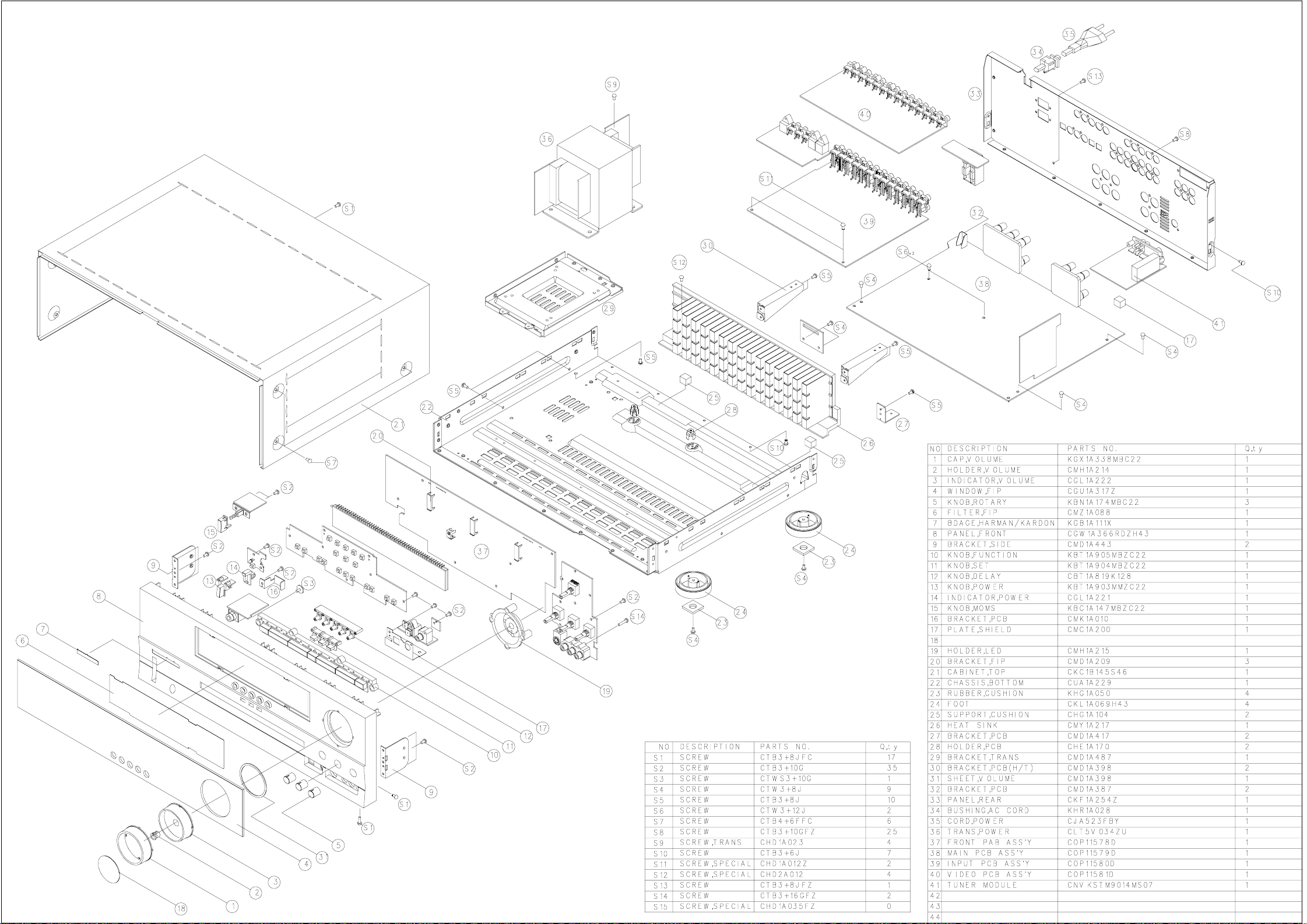
AVR130 EXPLODED VIEW
22
ORNAMENT, VOLUME KNOB
CGU1A318Z
Page 23
AVR130 harman/kardon
23
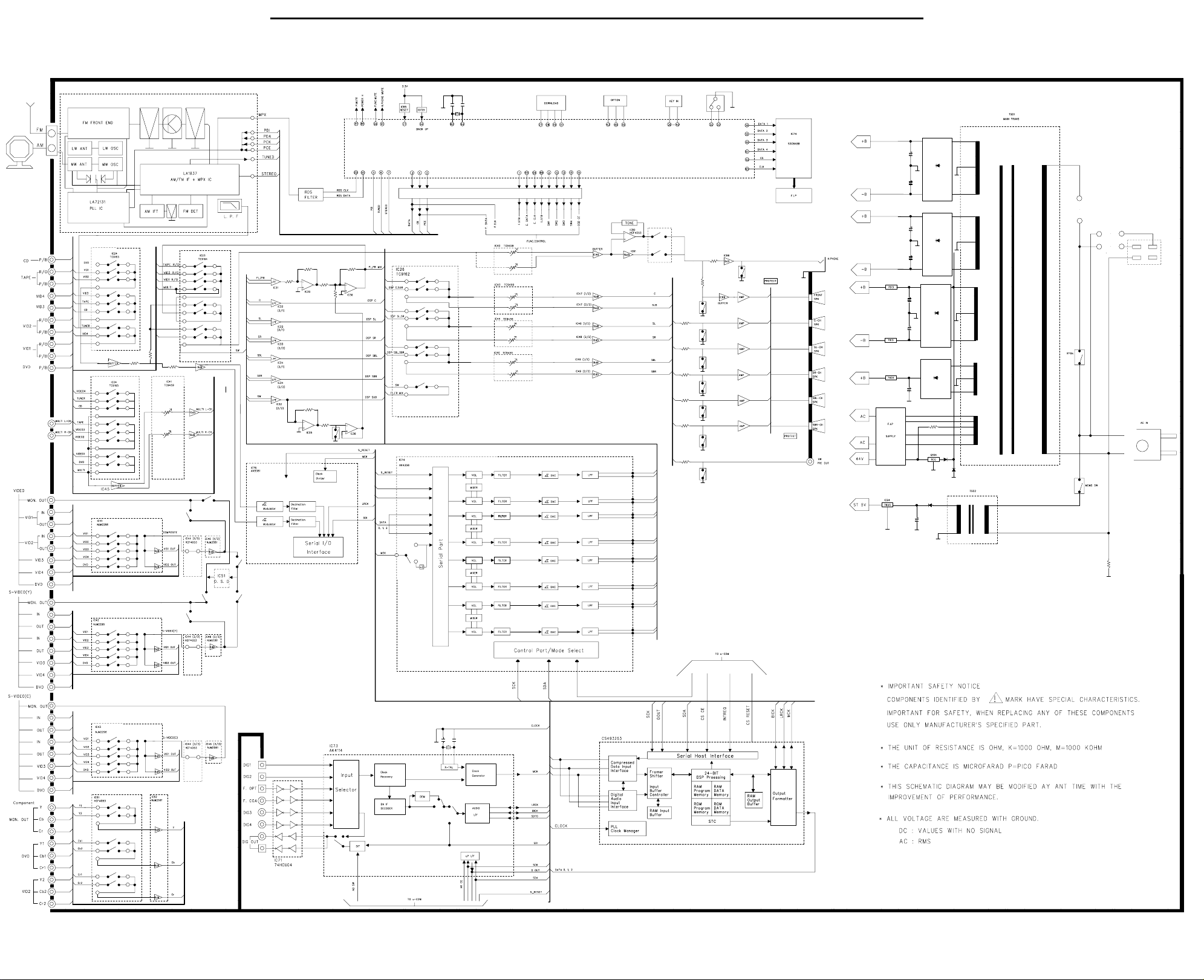
BLOCK DIAGRAM
Page 24
AVR130 harman/kardon
24
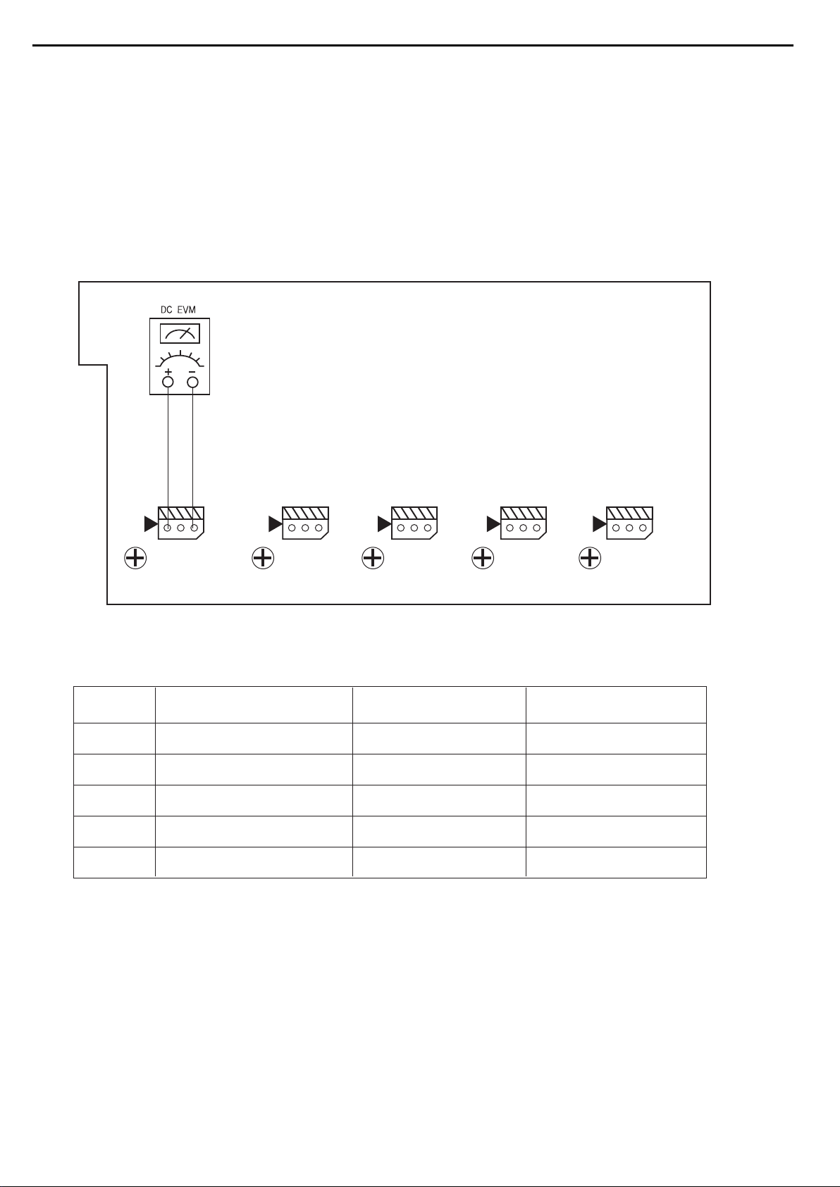
AMPLIFIER SECTION BIAS ADJUSTMENT
Measurement condition
. No input signal or volume position is minimum.
Standard value.
. Ideal current = 48mA ( ± 5%)
. Ideal DC Voltage = 25.92mV ( ± 5%)
CUP11651X (BIAS PCB)
...... ......
VR87
CN81
VR86
CN82
VR82
CN86
VR81
DC VOLTMETER..............Connect to CN81,CN82,CN83,CN84,CN85,CN86,CN87
NO. Channel Adjust for
1 Front Left 25.92mV (±5%)
2 Front Right 25.92mV (±5%)
3 Center
4 Surround Left
5 Surround Right
6
7
Surround Back Left
Surround Back Right
25.92mV (±5%)
25.92mV (±5%)
25.92mV (±5%)
25.92mV (±5%)
25.92mV (±5%)
Adjustment
VR82(ONLY AVR230/330)
VR81(ONLY AVR330)
CN87
VR83
VR84
VR85
VR86
VR87
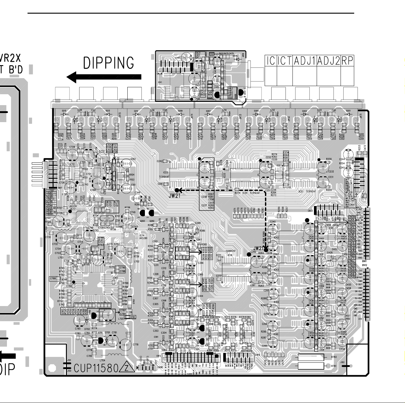
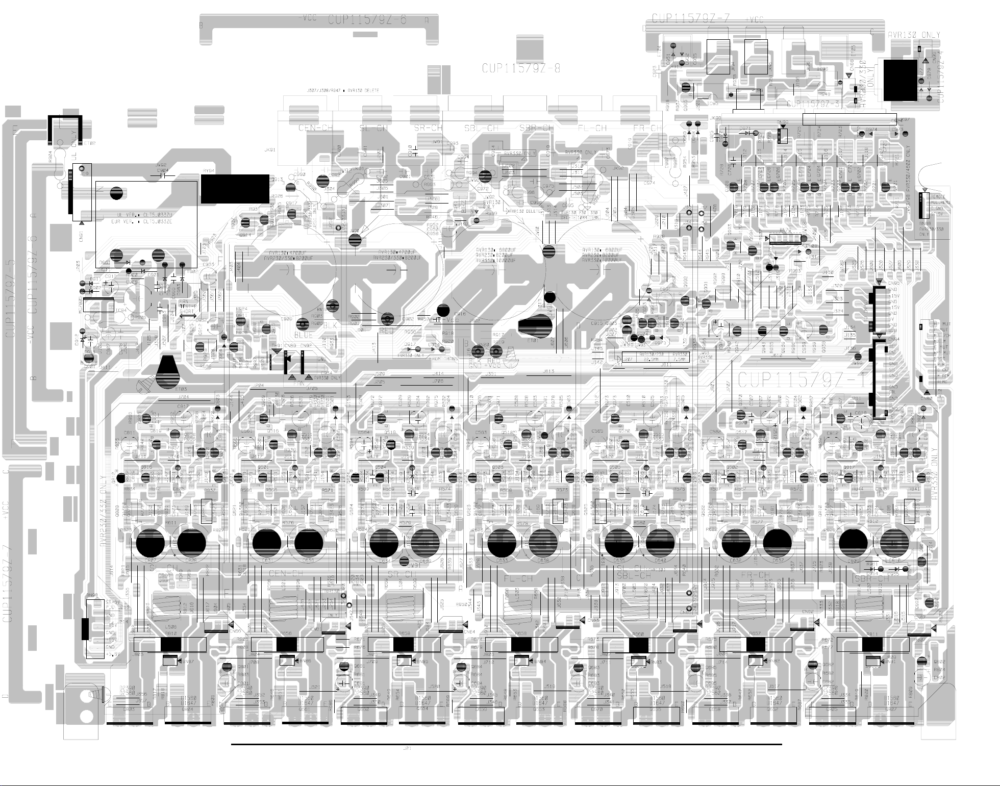
Page 25
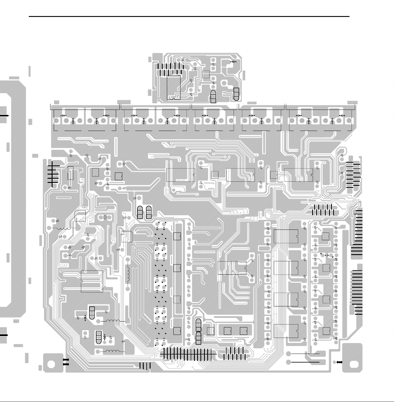
AVR130 harman/kardon
25
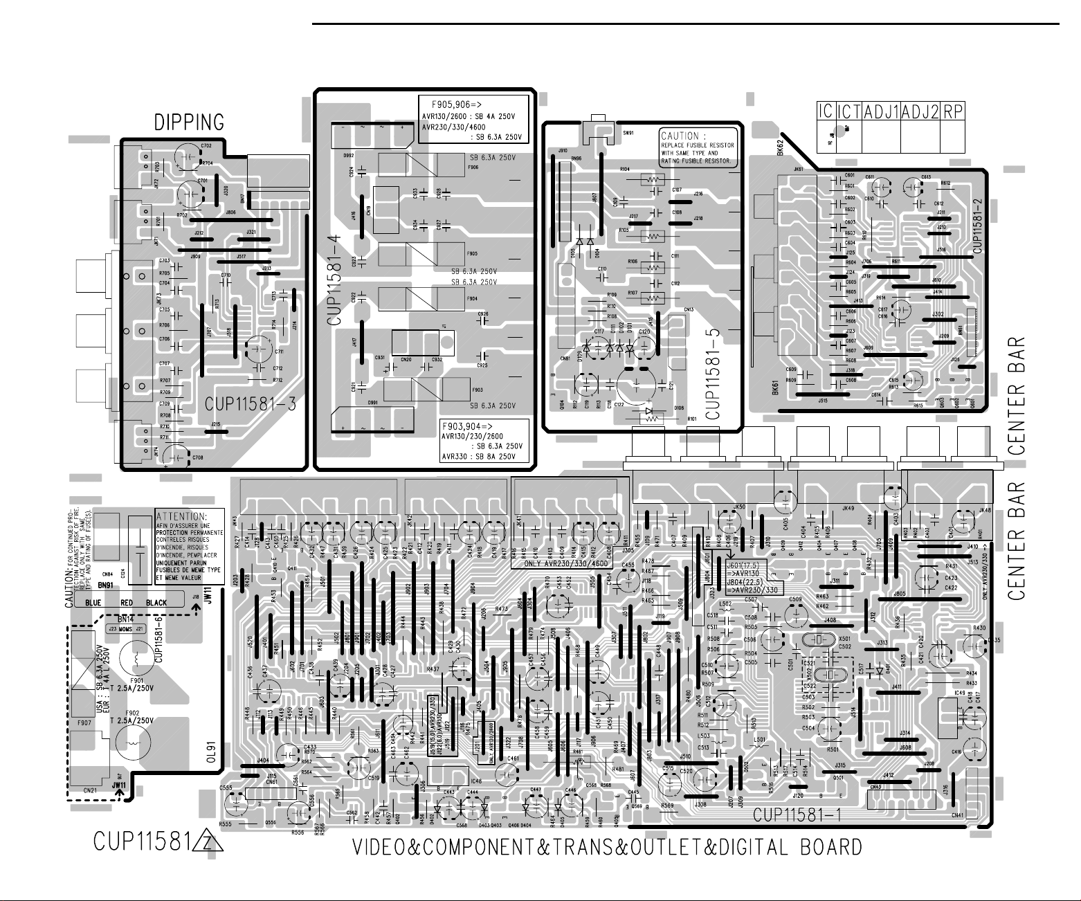
VIDEO BOARD
Page 26
AVR130 harman/kardon
26
FRONT BOARD
Page 27
AVR130 harman/kardon
27
BOTTOM VIEW
INPUT BOARD
Page 28
AVR130 harman/kardon
28
TOP VIEW
INPUT BOARD
Page 29
CAM350PROV7.6:MonSep0110:29:562003-(Untitled)
29
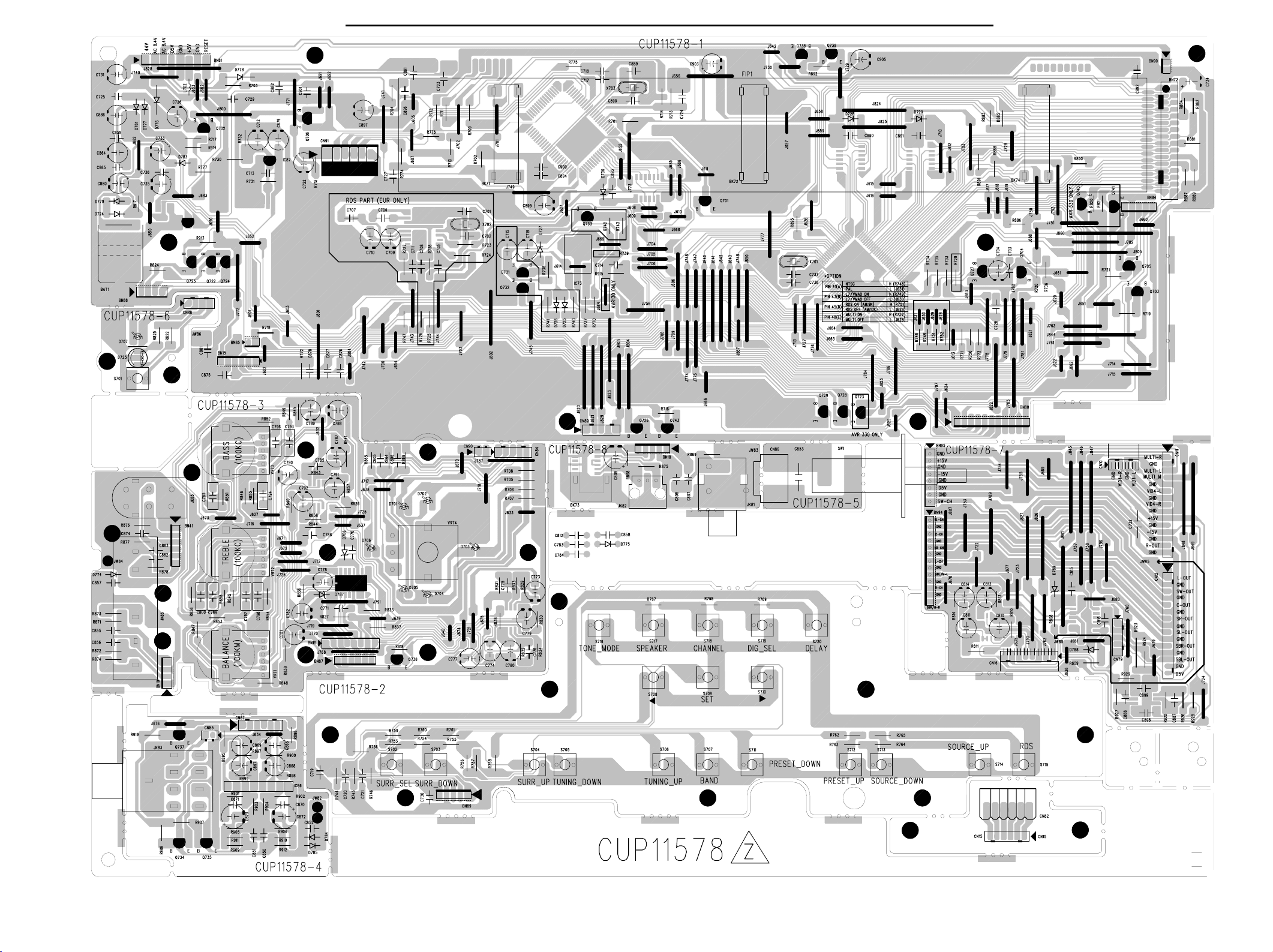
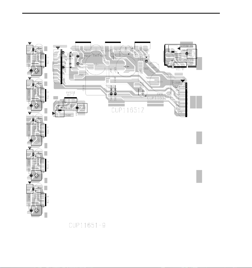
MAIN BOARD 1 (AMP)
AVR130 harman/kardon
Page 30
AVR130 harman/kardon
30
MAIN BOARD 2 (BIAS & REGULATOR)
Page 31

AVR130 harman/kardon
31
AVR130 Electrical Parts List
Ref. Designator Part Number Description
FRONT PCB ASS'Y
Capacitors
C703 HCBS1H821KBT CAP , CERAMIC 820PF 50V K
C704 HCEA1VH100T CAP , ELECT 10UF 35V
C712 HCEA1HH1R0T CAP , ELECT 1UF 50V
C713 HCBS1H223ZFT CAP , CERAMIC 0.022UF 50V Z
C714 HCBS1H151KBT CAP , CERAMIC 150PF 50V K
C716 HCEA1CH331T CAP , ELECT 330UF 16V
C717 HCBS1H221KBT CAP , CERAMIC 220PF 50V K
C718 HCBS1H221KBT CAP , CERAMIC 220PF 50V K
C719 HCBS1H181KBT CAP , CERAMIC 180PF 50V K
C720 HCBS1H181KBT CAP , CERAMIC 180PF 50V K
C721 HCBS1H181KBT CAP , CERAMIC 180PF 50V K
C722 HCEA1CH101T CAP , ELECT 100UF 16V
C723 HCBS1H104ZFT CAP , CERAMIC 0.1UF 50V Z
C724 HCBS1H223ZFT CAP , CERAMIC 0.022UF 50V Z
C725 CCKT1H473ZF CAP , CERAMIC 0.047UF 50V ZF
C726 HCEA0JH102T CAP , ELECT 1000UF 6.3V
C727 HCBS1H221KBT CAP , CERAMIC 220PF 50V K
C728 HCBS1H104ZFT CAP , CERAMIC 0.1UF 50V Z
C729 CCKT1H473ZF CAP , CERAMIC 0.047UF 50V ZF
C730 HCBS1H104ZFT CAP , CERAMIC 0.1UF 50V Z
C731 HCEA1HH100T CAP , ELECT 10UF 50V
C732 HCBS1H104ZFT CAP , CERAMIC 0.1UF 50V Z
C733 HCEA1EH470T CAP , ELECT 47UF 25V
C735 HCEA1VH100T CAP , ELECT 10UF 35V
C736 HCBS1H223ZFT CAP , CERAMIC 0.022UF 50V Z
C737 HCBS1H180JT CAP , CERAMIC 18PF 50V
C738 HCBS1H180JT CAP , CERAMIC 18PF 50V
C770 HCBS1H223ZFT CAP , CERAMIC 0.022UF 50V Z
C771 HCBS1H223ZFT CAP , CERAMIC 0.022UF 50V Z
C773 HCEA1VH100T CAP , ELECT 10UF 35V
C774 HCEA1VH100T CAP , ELECT 10UF 35V
C775 HCBS1H151KBT CAP , CERAMIC 150PF 50V K
C776 HCBS1H151KBT CAP , CERAMIC 150PF 50V K
C777 HCEA1VH100T CAP , ELECT 10UF 35V
C778 HCEA1VH100T CAP , ELECT 10UF 35V
C779 HCEA1CKS470T CAP, ELECT 47UF 16V
C780 HCEA1CKS470T CAP, ELECT 47UF 16V
C781 HCEA1CKS100T CAP , ELECT 10UF 16V
C782 HCEA1CKS100T CAP , ELECT 10UF 16V
C785 HCBS1H470JT CAP , CERAMIC 47PF 50V J
C786 HCBS1H470JT CAP , CERAMIC 47PF 50V J
C787 HCEA1CKS100T CAP , ELECT 10UF 16V
C788 HCEA1CKS100T CAP , ELECT 10UF 16V
C789 HCEA1CKS100T CAP , ELECT 10UF 16V
C790 HCEA1CKS100T CAP , ELECT 10UF 16V
C791 HCEA1CKS470T CAP, ELECT 47UF 16V
C792 HCEA1CKS470T CAP, ELECT 47UF 16V
C793 KCFE1J183JBT CAP , FILM 0.018UF 63V J
C794 KCFE1J183JBT CAP , FILM 0.018UF 63V J
C795 KCFE1J823JBT CAP , FILM 0.082UF 63V J
C796 KCFE1J823JBT CAP , FILM 0.082UF 63V J
C797 KCFE1J332JBT CAP , FILM 0.0033UF 63V J
C798 KCFE1J332JBT CAP , FILM 0.0033UF 63V J
C799 KCFE1J183JBT CAP , FILM 0.018UF 63V J
C800 KCFE1J183JBT CAP , FILM 0.018UF 63V J
C805 HCBS1H223ZFT CAP , CERAMIC 0.022UF 50V Z
Page 32

AVR130 harman/kardon
32
Ref. Designator Part Number Description
FRONT PCB ASS'Y
C806 HCBS1H223ZFT CAP , CERAMIC 0.022UF 50V Z
C807 CCKT1H104ZF CAP , CERAMIC 50V 0.1UF
C808 CCKT1H181KB CAP , CERAMIC 180PF 50V KB
C809 HCEA1AH471T CAP , ELECT 470UF 10V
C810 HCEA1CH101T CAP , ELECT 100UF 16V
C811 HCEA1CH101T CAP , ELECT 100UF 16V
C812 HCBS1H104ZFT CAP , CERAMIC 0.1UF 50V Z
C813 HCEA1HH4R7T CAP , ELECT 4.7UF 50V
C814 HCEA1HH4R7T CAP , ELECT 4.7UF 50V
C850 HCBS1H471KBT CAP , CERAMIC 470PF 50V
C851 HCBS1H471KBT CAP , CERAMIC 470PF 50V
C852 HCBS1H104ZFT CAP , CERAMIC 0.1UF 50V Z
C855 HCBS1H101KBT CAP , CERAMIC 100PF 50V K
C856 HCBS1H101KBT CAP , CERAMIC 100PF 50V K
C857 HCBS1H104ZFT CAP , CERAMIC 0.1UF 50V Z
C858 HCBS1H223ZFT CAP , CERAMIC 0.022UF 50V Z
C859 HCBS1H223ZFT CAP , CERAMIC 0.022UF 50V Z
C860 HCBS1H223ZFT CAP , CERAMIC 0.022UF 50V Z
C861 HCBS1H223ZFT CAP , CERAMIC 0.022UF 50V Z
C862 HCBS1H101KBT CAP , CERAMIC 100PF 50V K
C863 HCBS1H101KBT CAP , CERAMIC 100PF 50V K
C864 HCEA1VH100T CAP , ELECT 10UF 35V
C865 CCKT1H473ZF CAP , CERAMIC 0.047UF 50V ZF
C866 HCEA1CKS100T CAP , ELECT 10UF 16V
C867 HCEA1CKS100T CAP , ELECT 10UF 16V
C868 HCEA1CKS470T CAP, ELECT 47UF 16V
C869 HCEA1CKS470T CAP, ELECT 47UF 16V
C870 HCBS1H681KBT CAP , CERAMIC 680PF 50V
C871 HCBS1H681KBT CAP , CERAMIC 680PF 50V
C872 HCEA1CH331T CAP , ELECT 330UF 16V
C873 HCEA1CH331T CAP , ELECT 330UF 16V
C874 HCBS1H101KBT CAP , CERAMIC 100PF 50V K
C875 HCBS1H473ZFT CAP , CERAMIC 0.047UF 50V Z
C876 HCBS1H473ZFT CAP , CERAMIC 0.047UF 50V Z
C877 HCBS1H473ZFT CAP , CERAMIC 0.047UF 50V Z
C878 HCBS1H473ZFT CAP , CERAMIC 0.047UF 50V Z
C880 HCEA1AH221T CAP , ELECT 220UF 10V
C882 HCBS1H104ZFT CAP , CERAMIC 0.1UF 50V Z
C886 HCEA0JH102T CAP , ELECT 1000UF 6.3V
C889 HCBS1H220JT CAP , CERAMIC 22PF 50V
C890 HCBS1H220JT CAP , CERAMIC 22PF 50V
C891 HCBS1H223ZFT CAP , CERAMIC 0.022UF 50V Z
C892 HCBS1H223ZFT CAP , CERAMIC 0.022UF 50V Z
C893 HCBS1H223ZFT CAP , CERAMIC 0.022UF 50V Z
C894 HCBS1H223ZFT CAP , CERAMIC 0.022UF 50V Z
C895 HCEA1AH471T CAP , ELECT 470UF 10V
C896 HCBS1H223ZFT CAP , CERAMIC 0.022UF 50V Z
C897 HCEA1AH471T CAP , ELECT 470UF 10V
C900 HCBS1H104ZFT CAP , CERAMIC 0.1UF 50V Z
C853 KCKDKS472ME CAP , CERAMIC(X1/Y2/SC) 0.0047UF/2.5KV
Semiconductors
D724 HVD1SS133MT DIODE 1SS133T-77
D728 HVD1SS133MT DIODE 1SS133T-77
D729 HVD1SS133MT DIODE 1SS133T-77
D730 HVD1SS133MT DIODE 1SS133T-77
D761 HVD1SS133MT DIODE 1SS133T-77
D774 HVD1SS133MT DIODE 1SS133T-77
D775 HVD1SS133MT DIODE 1SS133T-77
D776 KVD1N4003ST DIODE 1N4003
Page 33

AVR130 harman/kardon
33
Ref. Designator Part Number Description
FRONT PCB ASS'Y
D777 HVD1SS133MT DIODE 1SS133T-77
D778 KVD1N4003ST DIODE 1N4003
D779 HVD1SS133MT DIODE 1SS133T-77
D783 HVD1SS133MT DIODE 1SS133T-77
D784 HVD1SS133MT DIODE 1SS133T-77
D785 HVD1SS133MT DIODE 1SS133T-77
D786 HVDMTZJ5.6BT DIODE , ZENER 5.6V ZENER
D787 HVDMTZJ5.6BT DIODE , ZENER 5.6V ZENER
IC87 HVIRE5VL28CATZ IC , RESET 2.8V I.C , RESET
Q701 HVTKRC107MT TRANSISTOR NPN KRC107M
Q702 HVTKRC107MT TRANSISTOR NPN KRC107M
Q703 HVTKRC107MT TRANSISTOR NPN KRC107M
Q705 HVTKRC107MT TRANSISTOR NPN KRC107M
Q706 HVTKRC107MT TRANSISTOR NPN KRC107M
Q722 HVTKRA107MT TRANSISTOR NPN KRA107M
Q724 HVTKRC107MT TRANSISTOR NPN KRC107M
Q725 HVTKRC107MT TRANSISTOR NPN KRC107M
Q726 HVTKRC107MT TRANSISTOR NPN KRC107M
Q727 HVTKRC107MT TRANSISTOR NPN KRC107M
Q728 HVTKRC107MT TRANSISTOR NPN KRC107M
Q729 HVTKRC107MT TRANSISTOR NPN KRC107M
Q734 HVTKTC2874BT TRANSISTOR , NPN, MUTE KTC2874B
Q735 HVTKTC2874BT TRANSISTOR , NPN, MUTE KTC2874B
Q736 HVTKTC2874BT TRANSISTOR , NPN, MUTE KTC2874B
Q737 HVTKTC2874BT TRANSISTOR , NPN, MUTE KTC2874B
Q738 HVTKRC107MT TRANSISTOR NPN KRC107M
Q739 HVTKTA1271YT TRANSISTOR PNP KTA1271Y
Q743 HVTKRA107MT TRANSISTOR NPN KRA107M
D702 CVD52CSBBCEAB2 BLUE L.E.D
D703 CVD52CSBBCEAB2 BLUE L.E.D
D704 CVD52CSBBCEAB2 BLUE L.E.D
D706 CVD52CSBBCEAB2 BLUE L.E.D
D707 CVD52CSBBCEAB2 BLUE L.E.D
D723 CVD50BOBBWGA L.E.D , 2 COLOR
IC72 BVIMB90F482APFG130 IC , FLASH U-COM FUJITSU
IC73 HRVRPM6938H4 SENSOR , REMOTE RPM6938-H4
IC74 HVIS3F84BB I.C , FLASH U-COM S3F84BB
IC75 HVI74ACT04MTR I.C , HEX
IC76 HVITC74HCU04AFN IC , INVERTER TC74HCU04AFN
IC80 HVIHCF4053M013T I.C S.T
IC81 HVINJM2068MDTE1 I.C , OP AMP NJM2068MD-TE1
IC82 HVINJM2068MDTE1 I.C , OP AMP NJM2068MD-TE1
IC83 HVI74ACT04MTR I.C , HEX
IC84 HVI74ACT04MTR I.C , HEX
IC85 HVIRH5VT18C I.C , RESET 1.8V I.C , RESET
IC86 HVINJM4556AL I.C NJM4556AL
IC88 HVINJM2068MDTE1 I.C , OP AMP NJM2068MD-TE1
Resistors
R701 CRD20TJ103T RES , CARBON 10K OHM 1/5W J
R702 CRD20TJ1R0T RES , CARBON 1 OHM 1/5W J
R704 CRD20TJ100T RES , CARBON 10 OHM 1/5W J
R705 CRD20TJ820T RES , CARBON 82 OHM 1/5W J
R706 CRD20TJ820T RES , CARBON 82 OHM 1/5W J
R707 CRD20TJ820T RES , CARBON 82 OHM 1/5W J
R708 CRD20TJ820T RES , CARBON 82 OHM 1/5W J
R709 CRD20TJ470T RES , CARBON 47 OHM 1/5W J
R710 CRD20TJ470T RES , CARBON 47 OHM 1/5W J
R711 CRD20TJ470T RES , CARBON 47 OHM 1/5W J
R712 CRD20TJ470T RES , CARBON 47 OHM 1/5W J
Page 34

AVR130 harman/kardon
34
Ref. Designator Part Number Description
FRONT PCB ASS'Y
R713 CRD20TJ332T RES , CARBON 3.3K OHM 1/5W J
R714 CRD20TJ470T RES , CARBON 47 OHM 1/5W J
R715 CRD20TJ470T RES , CARBON 47 OHM 1/5W J
R716 CRD20TJ102T RES , CARBON 1K OHM 1/5W J
R717 CRD20TJ103T RES , CARBON 10K OHM 1/5W J
R718 CRD20TJ222T RES , CARBON 2.2K OHM 1/5W J
R719 CRD20TJ102T RES , CARBON 1K OHM 1/5W J
R721 CRD20TJ103T RES , CARBON 10K OHM 1/5W J
R730 CRD20TJ112T RES,CABON 1.1K OHM 1/5W J
R731 CRD20TJ223T RES , CARBON 22K OHM 1/5W J
R732 CRD20TJ202T RES , CARBON 2K OHM 1/5W J
R733 CRD20TJ272T RES , CARBON 2.7K OHM 1/5W J
R734 CRD20TJ103T RES , CARBON 10K OHM 1/5W J
R735 CRD20TJ103T RES , CARBON 10K OHM 1/5W J
R736 CRD20TJ272T RES , CARBON 2.7K OHM 1/5W J
R737 CRD20TJ100T RES , CARBON 10 OHM 1/5W J
R744 CRD20TJ103T RES , CARBON 10K OHM 1/5W J
R745 CRD20TJ103T RES , CARBON 10K OHM 1/5W J
R746 CRD20TJ103T RES , CARBON 10K OHM 1/5W J
R747 CRD20TJ103T RES , CARBON 10K OHM 1/5W J
R748 CRD20TJ223T RES , CARBON 22K OHM 1/5W J
R749 CRD20TJ223T RES , CARBON 22K OHM 1/5W J
R750 CRD20TJ223T RES , CARBON 22K OHM 1/5W J
R753 CRD20TJ102T RES , CARBON 1K OHM 1/5W J
R754 CRD20TJ152T RES , CARBON 1.5K OHM 1/5W J
R755 CRD20TJ182T RES , CARBON 1.8K OHM 1/5W J
R756 CRD20TJ272T RES , CARBON 2.7K OHM 1/5W J
R757 CRD20TJ332T RES , CARBON 3.3K OHM 1/5W J
R758 CRD20TJ562T RES , CARBON 5.6K OHM 1/5W J
R759 CRD20TJ102T RES , CARBON 1K OHM 1/5W J
R760 CRD20TJ152T RES , CARBON 1.5K OHM 1/5W J
R761 CRD20TJ182T RES , CARBON 1.8K OHM 1/5W J
R762 CRD20TJ272T RES , CARBON 2.7K OHM 1/5W J
R763 CRD20TJ332T RES , CARBON 3.3K OHM 1/5W J
R764 CRD20TJ562T RES , CARBON 5.6K OHM 1/5W J
R765 CRD20TJ752T RES , CARBON 7.5K OHM 1/5W J
R766 CRD20TJ102T RES , CARBON 1K OHM 1/5W J
R767 CRD20TJ152T RES , CARBON 1.5K OHM 1/5W J
R768 CRD20TJ182T RES , CARBON 1.8K OHM 1/5W J
R769 CRD20TJ272T RES , CARBON 2.7K OHM 1/5W J
R771 CRD20TJ103T RES , CARBON 10K OHM 1/5W J
R772 CRD20TJ103T RES , CARBON 10K OHM 1/5W J
R773 CRD20TJ103T RES , CARBON 10K OHM 1/5W J
R774 CRD20TJ222T RES , CARBON 2.2K OHM 1/5W J
R775 CRD20TJ470T RES , CARBON 47 OHM 1/5W J
R776 CRD20TJ470T RES , CARBON 47 OHM 1/5W J
R777 CRD20TJ100T RES , CARBON 10 OHM 1/5W J
R810 CRD20TJ101T RES , CARBON 100 OHM 1/5W J
R811 CRD20TJ101T RES , CARBON 100 OHM 1/5W J
R813 CRD20TJ104T RES , CARBON 100K OHM 1/5W J
R814 CRD20TJ104T RES , CARBON 100K OHM 1/5W J
R822 CRD20TJ471T RES , CARBON 470 OHM 1/5W J
R824 CRD20TJ820T RES , CARBON 82 OHM 1/5W J
R825 CRD20TJ181T RES , CARBON 180 OHM 1/5W J
R826 CRD20TJ102T RES , CARBON 1K OHM 1/5W J
R827 CRD20TJ102T RES , CARBON 1K OHM 1/5W J
R829 CRD20TJ184T RES , CARBON 180K OHM 1/5W J
R830 CRD20TJ184T RES , CARBON 180K OHM 1/5W J
R831 CRD20TJ562T RES , CARBON 5.6K OHM 1/5W J
R832 CRD20TJ562T RES , CARBON 5.6K OHM 1/5W J
R833 CRD20TJ102T RES , CARBON 1K OHM 1/5W J
Page 35

AVR130 harman/kardon
35
Ref. Designator Part Number Description
FRONT PCB ASS'Y
R834 CRD20TJ102T RES , CARBON 1K OHM 1/5W J
R835 CRD20TJ184T RES , CARBON 180K OHM 1/5W J
R836 CRD20TJ184T RES , CARBON 180K OHM 1/5W J
R837 CRD20TJ101T RES , CARBON 100 OHM 1/5W J
R838 CRD20TJ101T RES , CARBON 100 OHM 1/5W J
R839 CRD20TJ104T RES , CARBON 100K OHM 1/5W J
R840 CRD20TJ104T RES , CARBON 100K OHM 1/5W J
R841 CRD20TJ473T RES , CARBON 47K OHM 1/5W J
R842 CRD20TJ473T RES , CARBON 47K OHM 1/5W J
R843 CRD20TJ105T RES , CARBON 1M OHM 1/5W J
R844 CRD20TJ105T RES , CARBON 1M OHM 1/5W J
R845 CRD20TJ104T RES , CARBON 100K OHM 1/5W J
R846 CRD20TJ104T RES , CARBON 100K OHM 1/5W J
R847 CRD20TJ102T RES , CARBON 1K OHM 1/5W J
R848 CRD20TJ102T RES , CARBON 1K OHM 1/5W J
R849 CRD20TJ223T RES , CARBON 22K OHM 1/5W J
R850 CRD20TJ223T RES , CARBON 22K OHM 1/5W J
R851 CRD20TJ392T RES , CARBON 3.9K OHM 1/5W J
R852 CRD20TJ392T RES , CARBON 3.9K OHM 1/5W J
R853 CRD20TJ222T RES , CARBON 2.2K OHM 1/5W J
R854 CRD20TJ222T RES , CARBON 2.2K OHM 1/5W J
R855 CRD20TJ681T RES , CARBON 680 OHM 1/5W J
R856 CRD20TJ681T RES , CARBON 680 OHM 1/5W J
R857 CRD20TJ221T RES , CARBON 220 OHM 1/5W J
R858 CRD20TJ221T RES , CARBON 220 OHM 1/5W J
R864 CRD20TJ272T RES , CARBON 2.7K OHM 1/5W J
R865 CRD20TJ102T RES , CARBON 1K OHM 1/5W J
R866 CRD20TJ272T RES , CARBON 2.7K OHM 1/5W J
R868 CRD20TJ1R0T RES , CARBON 1 OHM 1/5W J
R869 CRD20TJ750T RES , CARBON 75 OHM 1/5W J
R871 CRD20TJ104T RES , CARBON 100K OHM 1/5W J
R872 CRD20TJ104T RES , CARBON 100K OHM 1/5W J
R873 CRD20TJ471T RES , CARBON 470 OHM 1/5W J
R874 CRD20TJ471T RES , CARBON 470 OHM 1/5W J
R875 CRD20TJ103T RES , CARBON 10K OHM 1/5W J
R876 CRD20TJ750T RES , CARBON 75 OHM 1/5W J
R877 CRD20TJ750T RES , CARBON 75 OHM 1/5W J
R878 CRD20TJ750T RES , CARBON 75 OHM 1/5W J
R881 CRD20TJ103T RES , CARBON 10K OHM 1/5W J
R882 CRD20TJ103T RES , CARBON 10K OHM 1/5W J
R883 CRD20TJ103T RES , CARBON 10K OHM 1/5W J
R884 CRD20TJ103T RES , CARBON 10K OHM 1/5W J
R885 CRD20TJ103T RES , CARBON 10K OHM 1/5W J
R886 CRD20TJ103T RES , CARBON 10K OHM 1/5W J
R887 CRD20TJ103T RES , CARBON 10K OHM 1/5W J
R888 CRD20TJ103T RES , CARBON 10K OHM 1/5W J
R889 CRD20TJ103T RES , CARBON 10K OHM 1/5W J
R890 CRD20TJ103T RES , CARBON 10K OHM 1/5W J
R891 CRD20TJ103T RES , CARBON 10K OHM 1/5W J
R892 CRD20TJ222T RES , CARBON 2.2K OHM 1/5W J
R893 CRD20TJ333T RES , CARBON 33K OHM 1/5W J
R895 CRD20TJ101T RES , CARBON 100 OHM 1/5W J
R896 CRD20TJ101T RES , CARBON 100 OHM 1/5W J
R897 CRD20TJ101T RES , CARBON 100 OHM 1/5W J
R898 CRD20TJ101T RES , CARBON 100 OHM 1/5W J
R899 CRD20TJ104T RES , CARBON 100K OHM 1/5W J
R900 CRD20TJ104T RES , CARBON 100K OHM 1/5W J
R901 CRD20TJ152T RES , CARBON 1.5K OHM 1/5W J
R902 CRD20TJ152T RES , CARBON 1.5K OHM 1/5W J
R903 CRD20TJ102T RES , CARBON 1K OHM 1/5W J
R904 CRD20TJ102T RES , CARBON 1K OHM 1/5W J
Page 36

AVR130 harman/kardon
36
Ref. Designator Part Number Description
FRONT PCB ASS'Y
R905 CRD20TJ104T RES , CARBON 100K OHM 1/5W J
R906 CRD20TJ104T RES , CARBON 100K OHM 1/5W J
R907 CRD20TJ562T RES , CARBON 5.6K OHM 1/5W J
R908 CRD20TJ562T RES , CARBON 5.6K OHM 1/5W J
R909 CRD20TJ221T RES , CARBON 220 OHM 1/5W J
R910 CRD20TJ221T RES , CARBON 220 OHM 1/5W J
R911 CRD20TJ221T RES , CARBON 220 OHM 1/5W J
R912 CRD20TJ221T RES , CARBON 220 OHM 1/5W J
R913 CRD20TJ102T RES , CARBON 1K OHM 1/5W J
R914 CRD20TJ473T RES , CARBON 47K OHM 1/5W J
R915 CRD20TJ473T RES , CARBON 47K OHM 1/5W J
R917 CRD20TJ123T RES , CARBON 12K OHM 1/5W J
R918 CRD20TJ562T RES , CARBON 5.6K OHM 1/5W J
R919 CRD20TJ562T RES , CARBON 5.6K OHM 1/5W J
VR71 CVV2X05M104Z RES , VARIABLE(BALANCE) RK14128030214Y
VR72 CVV2X07C104Z RES , VARIABLE(TONE) RK14128030214C
VR73 CVV2X07C104Z RES , VARIABLE(TONE) RK14128030214C
Miscellaneous
VR74 HSR2A029Z VR , ENCODER
FIP1 HFLHCA18ML01 F.I.P SAMSUNG S.D.I
L702 HLQ02C100KT COIL , AXAIL 10UH
S701 HST1A020ZT SW , TACT
S702 HST1A020ZT SW , TACT
S703 HST1A020ZT SW , TACT
S704 HST1A020ZT SW , TACT
S705 HST1A020ZT SW , TACT
S706 HST1A020ZT SW , TACT
S707 HST1A020ZT SW , TACT
S708 HST1A020ZT SW , TACT
S709 HST1A020ZT SW , TACT
S710 HST1A020ZT SW , TACT
S711 HST1A020ZT SW , TACT
S712 HST1A020ZT SW , TACT
S713 HST1A020ZT SW , TACT
S714 HST1A020ZT SW , TACT
S715 HST1A020ZT SW , TACT
S716 HST1A020ZT SW , TACT
S717 HST1A020ZT SW , TACT
S718 HST1A020ZT SW , TACT
S719 HST1A020ZT SW , TACT
S720 HST1A020ZT SW , TACT
BAT1 HABGP40BVH3A3H BATTERY , RECHARGEABLE GP40BBVH3A3H
BK71 CMD1A209 BRACKET , FLT A4-92-1739
BK72 CMD1A209 BRACKET , FLT A4-92-1739
BK73 CMD1A387 BRACKET , PCB
BK74 CMD1A209 BRACKET , FLT A4-92-1739
BN10 CWZAVR230BN10 WIRE ASS'Y (SHIELD)
BN15 CWB2B906150EN WIRE ASS'Y
BN16 CWZAVR2550BN16 WIRE ASS'Y (SHIELD)
BN18 CWZAVR125BN18 WIRE ASS'Y (SHIELD)
BN41 CWZAVR130BN41 WIRE ASS'Y (SHIELD)
BN80 CWB2B911420EW WIRE ASS'Y
BN81 CWB2B908250BM WIRE , ASS'Y
BN84 CWB2B905080EN WIRE ASS'Y
BN85 CWB2B902090EN WIRE ASS'Y
BN87 CWZAVR2550BN87 WIRE ASS'Y (SHIELD)
BN88 CWB2B904070EN WIRE ASS'Y
BN89 CWB2B905080EN WIRE ASS'Y
BN90 CWB2B902090EN WIRE ASS'Y
Page 37

AVR130 harman/kardon
37
Ref. Designator Part Number Description
FRONT PCB ASS'Y
BN94 KJP13GB99ZM CONNECTOR MOLEX35237-1310
BN95 KJP08GB99ZM CONNECTOR , HOUSING MOLEX35237-0810
CN10 KJP04GB46ZM WAFER MOLEX 53015
CN11 KJP15GA98ZM WAFER MOLEX35336-1510
CN12 KJP15GA98ZM WAFER MOLEX35336-1510
CN15 KJP06GA19ZM WAFER MOLEX53014-0610
CN16 KJP08GB46ZM WAFER
CN72 KJP32GA161ZY WAFER YD200 SERIES
CN82 KJP06HA37ZM WAFER MOLEX42140-2206
CN84 KJP05GA19ZM WAFER MOLEX53014-0510
CN85 KJP02GA19ZM WAFER
CN86 KJP02GA89ZM WAFER MOLEX35328-02
CN87 KJP06GA19ZM WAFER MOLEX53014-0610
CN88 KJP04GA19ZM WAFER
CN89 KJP05GA19ZM WAFER MOLEX53014-0510
CN90 KJP02GA19ZM WAFER
CN91 KJP06HA37ZM WAFER MOLEX42140-2206
JK81 CJJ4M041Y JACK , BOARD (COAX)
JK82 HJSTORX179L MODULE , OPTICAL(RX) TORX179L
JK83 CJJ2E026Z JACK , HEADPHONE(SILVER PLATE)
JK85 CJJ9M003Z JACK , S-VIDEO
JK86 CJJ4S023Y JACK , BOARD
JW82 CWZAVR2550JW82 WIRE , ASS'Y
JW84 CWE8202110RV WIRE, ASS'Y
JW85 CWE8202070AA WIRE ASS'Y
SW01 CSH1A008ZV SW , PUSH (MOMS)
X701 HOX05000E160C CRYSTAL 5 MHz
X703 HOX10000E220C CRYSTAL 10 MHz
CTB3+10G SCREW
CTB3+16GFZ SCREW
CTWS3+10G SCREW
KBC1A147MBZC22 KNOB , MOMS
KBT1A903MMZC22 KNOB , POWER
KBT1A904MBZC22 KNOB , SET
KBT1A905MBZC22 KNOB , FUNCTIION
KHR301 CLAMPER
BN72 CWZAVR230BN72 WIRE ASS'Y
CKC1B145S46 CABINET , TOP
CLZ9Z028Z FERRITE CORE(21.2X6.4X12.7) K5C T
CMH1A214 HOLDER , VOLUME
CMZ1A090 SHEET , VOLUME
CTB3+8JFC SCREW
CTB4+6FFC SCREW
MAIN PCB ASS'Y
Capacitors
C501 HCEA1VH100T CAP , ELECT 10UF 35V
C502 HCEA1VH100T CAP , ELECT 10UF 35V
C503 HCEA1VH100T CAP , ELECT 10UF 35V
C504 HCEA1VH100T CAP , ELECT 10UF 35V
C505 HCEA1VH100T CAP , ELECT 10UF 35V
C506 CCKT1H331KB CAP , CERAMIC 330PF 50V KB
C507 CCKT1H331KB CAP , CERAMIC 330PF 50V KB
C508 CCKT1H331KB CAP , CERAMIC 330PF 50V KB
C509 CCKT1H331KB CAP , CERAMIC 330PF 50V KB
C510 CCKT1H331KB CAP , CERAMIC 330PF 50V KB
C561 HCEA1CH101T CAP , ELECT 100UF 16V
C562 HCEA1CH101T CAP , ELECT 100UF 16V
Page 38

AVR130 harman/kardon
38
Ref. Designator Part Number Description
MAIN PCB ASS'Y
C563 HCEA1CH101T CAP , ELECT 100UF 16V
C564 HCEA1CH101T CAP , ELECT 100UF 16V
C565 HCEA1CH101T CAP , ELECT 100UF 16V
C566 HCEA1CH101T CAP , ELECT 100UF 16V
C567 HCEA1CH101T CAP , ELECT 100UF 16V
C568 HCEA1CH101T CAP , ELECT 100UF 16V
C569 HCEA1CH101T CAP , ELECT 100UF 16V
C570 HCEA1CH101T CAP , ELECT 100UF 16V
C571 HCBS1H681KBT CAP , CERAMIC 680PF 50V
C572 HCBS1H681KBT CAP , CERAMIC 680PF 50V
C573 HCBS1H681KBT CAP , CERAMIC 680PF 50V
C574 HCBS1H681KBT CAP , CERAMIC 680PF 50V
C575 HCBS1H681KBT CAP , CERAMIC 680PF 50V
C601 CCCT1H120JC CAP , CERAMIC 12PF 50V JC
C602 CCCT1H120JC CAP , CERAMIC 12PF 50V JC
C603 CCCT1H120JC CAP , CERAMIC 12PF 50V JC
C604 CCCT1H120JC CAP , CERAMIC 12PF 50V JC
C605 CCCT1H120JC CAP , CERAMIC 12PF 50V JC
C606 CCCT1H330JC CAP , CERAMIC 33PF 50V JC
C607 CCCT1H330JC CAP , CERAMIC 33PF 50V JC
C608 CCCT1H330JC CAP , CERAMIC 33PF 50V JC
C609 CCCT1H330JC CAP , CERAMIC 33PF 50V JC
C610 CCCT1H330JC CAP , CERAMIC 33PF 50V JC
C681 HCEA1HH100T CAP , ELECT 10UF 50V
C682 HCEA1HH100T CAP , ELECT 10UF 50V
C683 HCEA1HH100T CAP , ELECT 10UF 50V
C684 HCEA1HH100T CAP , ELECT 10UF 50V
C685 HCEA1HH100T CAP , ELECT 10UF 50V
C726 CCKT1H221KB CAP , MYLAR 220PF 50V KB
C900 HCQI1H473JZT CAP , MYLAR 0.047UF 50V J
C901 HCQI1H473JZT CAP , MYLAR 0.047UF 50V J
C905 CCKT1H223ZF CAP , CERAMIC 0.022UF 50V ZF
C907 HCEA1CH101T CAP , ELECT 100UF 16V
C908 CCKT1H223ZF CAP , CERAMIC 0.022UF 50V ZF
C910 HCQI1H473JZT CAP , MYLAR 0.047UF 50V J
C911 HCEA1CH471T CAP , ELECT 470UF 16V
C912 HCEA1CH221T CAP , ELECT 220UF 16V
C913 CCFT1H104ZF CAP , SEMICONDUCTOR 0.1UF 50V ZF
C918 HCQI1H473JZT CAP , MYLAR 0.047UF 50V J
C919 HCQI1H473JZT CAP , MYLAR 0.047UF 50V J
C939 HCEA1HH4R7T CAP , ELECT 4.7UF 50V
C940 HCEA1AH471T CAP , ELECT 470UF 10V
C971 HCQI1H562JZT CAP , MYLAR 5600PF 50V J
C973 HCQI1H562JZT CAP , MYLAR 5600PF 50V J
C974 HCQI1H562JZT CAP , MYLAR 5600PF 50V J
C980 HCQI1H562JZT CAP , MYLAR 5600PF 50V J
C981 HCQI1H562JZT CAP , MYLAR 5600PF 50V J
C990 HCQI1H473JZT CAP , MYLAR 0.047UF 50V J
C991 HCEA1HH1R0T CAP , ELECT 1UF 50V
C992 HCQI1H473JZT CAP , MYLAR 0.047UF 50V J
C993 HCQI1H473JZT CAP , MYLAR 0.047UF 50V J
C995 HCQI1H473JZT CAP , MYLAR 0.047UF 50V J
C997 HCQI1H473JZT CAP , MYLAR 0.047UF 50V J
C999 CCKT1H223ZF CAP , CERAMIC 0.022UF 50V ZF
C631 CCEA1JH221E CAP , ELECT 220UF 63V
C632 CCEA1JH221E CAP , ELECT 220UF 63V
C633 CCEA1JH221E CAP , ELECT 220UF 63V
C634 CCEA1JH221E CAP , ELECT 220UF 63V
C635 CCEA1JH221E CAP , ELECT 220UF 63V
C636 CCEA1JH221E CAP , ELECT 220UF 63V
C637 CCEA1JH221E CAP , ELECT 220UF 63V
Page 39

AVR130 harman/kardon
39
Ref. Designator Part Number Description
MAIN PCB ASS'Y
C638 CCEA1JH221E CAP , ELECT 220UF 63V
C639 CCEA1JH221E CAP , ELECT 220UF 63V
C640 CCEA1JH221E CAP , ELECT 220UF 63V
C902 CCET50VKL4472NK CAP , ELECT 4700UF/50V
C904 KCKDKS472ME CAP , CERAMIC(X1/Y2/SC) 0.0047UF/2.5KV
C906 HCEA1EH102E CAP , ELECT 1000UF 25V
C909 CCET50VKL4472NK CAP , ELECT 4700UF/50V
C915 CCET50VKL4682NK CAP , ELECT 6800UF/50V
C916 CCET50VKL4682NK CAP , ELECT 6800UF/50V
Semiconductors
D501 HVD1SS133MT DIODE 1SS133T-77
D502 HVD1SS133MT DIODE 1SS133T-77
D503 HVD1SS133MT DIODE 1SS133T-77
D504 HVD1SS133MT DIODE 1SS133T-77
D505 HVD1SS133MT DIODE 1SS133T-77
D581 HVD1SS133MT DIODE 1SS133T-77
D582 HVD1SS133MT DIODE 1SS133T-77
D583 HVD1SS133MT DIODE 1SS133T-77
D584 HVD1SS133MT DIODE 1SS133T-77
D585 HVD1SS133MT DIODE 1SS133T-77
D901 KVD1N4003ST DIODE 1N4003
D902 HVD1SS133MT DIODE 1SS133T-77
D911 HVD1SS133MT DIODE 1SS133T-77
D912 HVD1SS133MT DIODE 1SS133T-77
D914 HVD1SS133MT DIODE 1SS133T-77
D917 HVD1SS133MT DIODE 1SS133T-77
D953 HVD1SS133MT DIODE 1SS133T-77
D954 KVD1N4003SRT DIODE TW 1N4003
D955 KVD1N4003SRT DIODE TW 1N4003
D961 KVD1N4003ST DIODE 1N4003
D962 KVD1N4003ST DIODE 1N4003
D963 KVD1N4003ST DIODE 1N4003
D977 HVD1SS133MT DIODE 1SS133T-77
D978 HVD1SS133MT DIODE 1SS133T-77
Q501 HVTKTA1268GRT TRANSISTOR PNP KTA1268GR
Q502 HVTKTA1268GRT TRANSISTOR PNP KTA1268GR
Q503 HVTKTA1268GRT TRANSISTOR PNP KTA1268GR
Q504 HVTKTA1268GRT TRANSISTOR PNP KTA1268GR
Q505 HVTKTA1268GRT TRANSISTOR PNP KTA1268GR
Q511 HVTKTC3200GRT TRANSISTOR NPN KTC3200GR
Q512 HVTKTC3200GRT TRANSISTOR NPN KTC3200GR
Q513 HVTKTC3200GRT TRANSISTOR NPN KTC3200GR
Q514 HVTKTC3200GRT TRANSISTOR NPN KTC3200GR
Q515 HVTKTC3200GRT TRANSISTOR NPN KTC3200GR
Q516 HVTKTC3200GRT TRANSISTOR NPN KTC3200GR
Q517 HVTKTC3200GRT TRANSISTOR NPN KTC3200GR
Q518 HVTKTC3200GRT TRANSISTOR NPN KTC3200GR
Q519 HVTKTC3200GRT TRANSISTOR NPN KTC3200GR
Q520 HVTKTC3200GRT TRANSISTOR NPN KTC3200GR
Q541 HVTKTC3198YT TRANSISTOR NPN KTC3198Y
Q542 HVTKTC3198YT TRANSISTOR NPN KTC3198Y
Q543 HVTKTC3198YT TRANSISTOR NPN KTC3198Y
Q544 HVTKTC3198YT TRANSISTOR NPN KTC3198Y
Q545 HVTKTC3198YT TRANSISTOR NPN KTC3198Y
Q556 HVTKTC3200GRT TRANSISTOR NPN KTC3200GR
Q557 HVTKTC3200GRT TRANSISTOR NPN KTC3200GR
Q558 HVTKTC3200GRT TRANSISTOR NPN KTC3200GR
Q559 HVTKTC3200GRT TRANSISTOR NPN KTC3200GR
Q560 HVTKTC3200GRT TRANSISTOR NPN KTC3200GR
Page 40

AVR130 harman/kardon
40
Ref. Designator Part Number Description
MAIN PCB ASS'Y
Q561 HVTKTC3200GRT TRANSISTOR NPN KTC3200GR
Q562 HVTKTC3200GRT TRANSISTOR NPN KTC3200GR
Q563 HVTKTC3200GRT TRANSISTOR NPN KTC3200GR
Q564 HVTKTC3200GRT TRANSISTOR NPN KTC3200GR
Q565 HVTKTC3200GRT TRANSISTOR NPN KTC3200GR
Q601 HVTKTA1268GRT TRANSISTOR PNP KTA1268GR
Q602 HVTKTA1268GRT TRANSISTOR PNP KTA1268GR
Q603 HVTKTA1268GRT TRANSISTOR PNP KTA1268GR
Q604 HVTKTA1268GRT TRANSISTOR PNP KTA1268GR
Q605 HVTKTA1268GRT TRANSISTOR PNP KTA1268GR
Q681 KVTKSC2785YT TRANSISTOR NPN KSC2785Y
Q682 KVTKSC2785YT TRANSISTOR NPN KSC2785Y
Q683 KVTKSC2785YT TRANSISTOR NPN KSC2785Y
Q684 KVTKSC2785YT TRANSISTOR NPN KSC2785Y
Q685 KVTKSC2785YT TRANSISTOR NPN KSC2785Y
Q706 HVTKTC2874BT TRANSISTOR, NPN, MUTE KTC2874B
Q901 KVTKSC2785YT TRANSISTOR NPN KSC2785Y
Q938 HVTKRA107MT TRANSISTOR NPN KRA107M
Q939 HVTKRA107MT TRANSISTOR NPN KRA107M
Q942 KVTKSC2785YT TRANSISTOR NPN KSC2785Y
Q943 KVTKSC2785YT TRANSISTOR NPN KSC2785Y
Q951 HVTKRC107MT TRANSISTOR NPN KRC107M
Q952 HVTKRA107MT TRANSISTOR NPN KRA107M
Q960 HVTKRC107MT TRANSISTOR NPN KRC107M
Q961 HVTKTA1024YT TRANSISTOR PNP KTA1024YT
Q969 HVTKTC2874BT TRANSISTOR, NPN, MUTE KTC2874B
Q970 HVTKTC2874BT TRANSISTOR, NPN, MUTE KTC2874B
Q971 HVTKTC2874BT TRANSISTOR, NPN, MUTE KTC2874B
Q972 HVTKTC2874BT TRANSISTOR, NPN, MUTE KTC2874B
Q973 HVTKTC2874BT TRANSISTOR, NPN, MUTE KTC2874B
Q991 HVTKRC107MT TRANSISTOR NPN KRC107M
Q992 HVTKRA107MT TRANSISTOR NPN KRA107M
Q652 BVT2SB1560-OKM TRANSISTOR, PNP, POWER 2SB1560
Q653 BVT2SB1560-OKM TRANSISTOR, PNP, POWER 2SB1560
Q654 BVT2SB1560-OKM TRANSISTOR, PNP, POWER 2SB1560
Q655 BVT2SB1560-OKM TRANSISTOR, PNP, POWER 2SB1560
Q657 BVT2SD2390-OKM TRANSISTOR, NPN, POWER 2SD2390
Q658 BVT2SD2390-OKM TRANSISTOR, NPN, POWER 2SD2390
Q659 BVT2SD2390-OKM TRANSISTOR, NPN, POWER 2SD2390
Q660 BVT2SD2390-OKM TRANSISTOR, NPN, POWER 2SD2390
Q661 BVT2SB1560-OKM TRANSISTOR, PNP, POWER 2SB1560
Q670 BVT2SD2390-OKM TRANSISTOR, NPN, POWER 2SD2390
Q858 HVT2SA1360O TRANSISTOR PNP 2SA1360
Q871 HVT2SA1360O TRANSISTOR PNP 2SA1360
Q872 HVT2SA1360O TRANSISTOR PNP 2SA1360
Q874 HVT2SA1360O TRANSISTOR PNP 2SA1360
Q875 HVT2SA1360O TRANSISTOR PNP 2SA1360
Q881 HVT2SC3423O TRANSISTOR NPN 2SC3423
Q882 HVT2SC3423O TRANSISTOR NPN 2SC3423
Q883 HVT2SC3423O TRANSISTOR NPN 2SC3423
Q884 HVT2SC3423O TRANSISTOR NPN 2SC3423
Q885 HVT2SC3423O TRANSISTOR NPN 2SC3423
IC94 HVIMC7805C I.C, REGULATOR KA7805-ABTU
Resistors
R501 CRD20TJ433T RES , CARBON 43K OHM 1/5W J
R502 CRD20TJ433T RES , CARBON 43K OHM 1/5W J
R503 CRD20TJ433T RES , CARBON 43K OHM 1/5W J
R504 CRD20TJ433T RES , CARBON 43K OHM 1/5W J
R505 CRD20TJ433T RES , CARBON 43K OHM 1/5W J
Page 41

AVR130 harman/kardon
41
Ref. Designator Part Number Description
MAIN PCB ASS'Y
R506 CRD20TJ333T RES , CARBON 33K OHM 1/5W J
R507 CRD20TJ333T RES , CARBON 33K OHM 1/5W J
R508 CRD20TJ333T RES , CARBON 33K OHM 1/5W J
R509 CRD20TJ333T RES , CARBON 33K OHM 1/5W J
R510 CRD20TJ333T RES , CARBON 33K OHM 1/5W J
R511 CRD20TJ152T RES , CARBON 1.5K OHM 1/5W J
R512 CRD20TJ152T RES , CARBON 1.5K OHM 1/5W J
R513 CRD20TJ152T RES , CARBON 1.5K OHM 1/5W J
R514 CRD20TJ152T RES , CARBON 1.5K OHM 1/5W J
R515 CRD20TJ152T RES , CARBON 1.5K OHM 1/5W J
R516 CRD20TJ152T RES , CARBON 1.5K OHM 1/5W J
R517 CRD20TJ152T RES , CARBON 1.5K OHM 1/5W J
R518 CRD20TJ152T RES , CARBON 1.5K OHM 1/5W J
R519 CRD20TJ152T RES , CARBON 1.5K OHM 1/5W J
R520 CRD20TJ152T RES , CARBON 1.5K OHM 1/5W J
R521 CRD20TJ471T RES , CARBON 470 OHM 1/5W J
R522 CRD20TJ471T RES , CARBON 470 OHM 1/5W J
R523 CRD20TJ471T RES , CARBON 470 OHM 1/5W J
R524 CRD20TJ471T RES , CARBON 470 OHM 1/5W J
R525 CRD20TJ471T RES , CARBON 470 OHM 1/5W J
R531 CRD20TJ221T RES , CARBON 220 OHM 1/5W J
R532 CRD20TJ221T RES , CARBON 220 OHM 1/5W J
R533 CRD20TJ221T RES , CARBON 220 OHM 1/5W J
R534 CRD20TJ221T RES , CARBON 220 OHM 1/5W J
R535 CRD20TJ221T RES , CARBON 220 OHM 1/5W J
R536 CRD20TJ221T RES , CARBON 220 OHM 1/5W J
R537 CRD20TJ221T RES , CARBON 220 OHM 1/5W J
R538 CRD20TJ221T RES , CARBON 220 OHM 1/5W J
R539 CRD20TJ221T RES , CARBON 220 OHM 1/5W J
R540 CRD20TJ221T RES , CARBON 220 OHM 1/5W J
R541 CRD20TJ271T RES , CARBON 270 OHM 1/5W J
R542 CRD20TJ271T RES , CARBON 270 OHM 1/5W J
R543 CRD20TJ271T RES , CARBON 270 OHM 1/5W J
R544 CRD20TJ271T RES , CARBON 270 OHM 1/5W J
R545 CRD20TJ271T RES , CARBON 270 OHM 1/5W J
R556 CRD20TJ273T RES , CARBON 27K OHM 1/5W J
R557 CRD20TJ273T RES , CARBON 27K OHM 1/5W J
R558 CRD20TJ273T RES , CARBON 27K OHM 1/5W J
R559 CRD20TJ273T RES , CARBON 27K OHM 1/5W J
R560 CRD20TJ273T RES , CARBON 27K OHM 1/5W J
R561 CRD20TJ202T RES , CARBON 2K OHM 1/5W J
R562 CRD20TJ202T RES , CARBON 2K OHM 1/5W J
R563 CRD20TJ202T RES , CARBON 2K OHM 1/5W J
R564 CRD20TJ202T RES , CARBON 2K OHM 1/5W J
R565 CRD20TJ202T RES , CARBON 2K OHM 1/5W J
R566 CRD20TJ561T RES , CARBON 560 OHM 1/5W J
R567 CRD20TJ561T RES , CARBON 560 OHM 1/5W J
R568 CRD20TJ561T RES , CARBON 560 OHM 1/5W J
R569 CRD20TJ561T RES , CARBON 560 OHM 1/5W J
R570 CRD20TJ561T RES , CARBON 560 OHM 1/5W J
R571 CRD20TJ561T RES , CARBON 560 OHM 1/5W J
R572 CRD20TJ561T RES , CARBON 560 OHM 1/5W J
R573 CRD20TJ561T RES , CARBON 560 OHM 1/5W J
R574 CRD20TJ561T RES , CARBON 560 OHM 1/5W J
R575 CRD20TJ561T RES , CARBON 560 OHM 1/5W J
R576 CRD20TJ100T RES , CARBON 10 OHM 1/5W J
R577 CRD20TJ100T RES , CARBON 10 OHM 1/5W J
R578 CRD20TJ100T RES , CARBON 10 OHM 1/5W J
R579 CRD20TJ100T RES , CARBON 10 OHM 1/5W J
R580 CRD20TJ100T RES , CARBON 10 OHM 1/5W J
R581 CRD20TJ561T RES , CARBON 560 OHM 1/5W J
Page 42

AVR130 harman/kardon
42
Ref. Designator Part Number Description
MAIN PCB ASS'Y
R582 CRD20TJ561T RES , CARBON 560 OHM 1/5W J
R583 CRD20TJ561T RES , CARBON 560 OHM 1/5W J
R584 CRD20TJ561T RES , CARBON 560 OHM 1/5W J
R585 CRD20TJ561T RES , CARBON 560 OHM 1/5W J
R586 CRD20TJ561T RES , CARBON 560 OHM 1/5W J
R587 CRD20TJ561T RES , CARBON 560 OHM 1/5W J
R588 CRD20TJ561T RES , CARBON 560 OHM 1/5W J
R589 CRD20TJ561T RES , CARBON 560 OHM 1/5W J
R590 CRD20TJ561T RES , CARBON 560 OHM 1/5W J
R591 CRD20TJ561T RES , CARBON 560 OHM 1/5W J
R592 CRD20TJ561T RES , CARBON 560 OHM 1/5W J
R593 CRD20TJ561T RES , CARBON 560 OHM 1/5W J
R594 CRD20TJ561T RES , CARBON 560 OHM 1/5W J
R595 CRD20TJ561T RES , CARBON 560 OHM 1/5W J
R596 CRD20TJ561T RES , CARBON 560 OHM 1/5W J
R597 CRD20TJ561T RES , CARBON 560 OHM 1/5W J
R598 CRD20TJ561T RES , CARBON 560 OHM 1/5W J
R599 CRD20TJ561T RES , CARBON 560 OHM 1/5W J
R600 CRD20TJ561T RES , CARBON 560 OHM 1/5W J
R601 CRD20TJ223T RES , CARBON 22K OHM 1/5W J
R602 CRD20TJ223T RES , CARBON 22K OHM 1/5W J
R603 CRD20TJ223T RES , CARBON 22K OHM 1/5W J
R604 CRD20TJ223T RES , CARBON 22K OHM 1/5W J
R605 CRD20TJ223T RES , CARBON 22K OHM 1/5W J
R606 CRD20TJ223T RES , CARBON 22K OHM 1/5W J
R607 CRD20TJ223T RES , CARBON 22K OHM 1/5W J
R608 CRD20TJ223T RES , CARBON 22K OHM 1/5W J
R609 CRD20TJ223T RES , CARBON 22K OHM 1/5W J
R610 CRD20TJ223T RES , CARBON 22K OHM 1/5W J
R631 KRD25FJ180T RES , CARBON 18 OHM 1/4W F
R632 KRD25FJ180T RES , CARBON 18 OHM 1/4W F
R633 KRD25FJ180T RES , CARBON 18 OHM 1/4W F
R634 KRD25FJ180T RES , CARBON 18 OHM 1/4W F
R635 KRD25FJ180T RES , CARBON 18 OHM 1/4W F
R636 KRD25FJ180T RES , CARBON 18 OHM 1/4W F
R637 KRD25FJ180T RES , CARBON 18 OHM 1/4W F
R638 KRD25FJ180T RES , CARBON 18 OHM 1/4W F
R639 KRD25FJ180T RES , CARBON 18 OHM 1/4W F
R640 KRD25FJ180T RES , CARBON 18 OHM 1/4W F
R646 KRD25FJ3R3T RES , CARBON 3.3 OHM 1/4W F
R647 KRD25FJ3R3T RES , CARBON 3.3 OHM 1/4W F
R648 KRD25FJ3R3T RES , CARBON 3.3 OHM 1/4W F
R649 KRD25FJ3R3T RES , CARBON 3.3 OHM 1/4W F
R650 KRD25FJ3R3T RES , CARBON 3.3 OHM 1/4W F
R651 KRD25FJ3R3T RES , CARBON 3.3 OHM 1/4W F
R652 KRD25FJ3R3T RES , CARBON 3.3 OHM 1/4W F
R653 KRD25FJ3R3T RES , CARBON 3.3 OHM 1/4W F
R654 KRD25FJ3R3T RES , CARBON 3.3 OHM 1/4W F
R655 KRD25FJ3R3T RES , CARBON 3.3 OHM 1/4W F
R666 CRD25TJ470T RES , CARBON 47 OHM 1/4W J
R667 CRD25TJ470T RES , CARBON 47 OHM 1/4W J
R668 CRD25TJ470T RES , CARBON 47 OHM 1/4W J
R669 CRD25TJ470T RES , CARBON 47 OHM 1/4W J
R670 CRD25TJ470T RES , CARBON 47 OHM 1/4W J
R671 CRD20TJ911T RES , CARBON 910 OHM 1/5W J
R672 CRD20TJ911T RES , CARBON 910 OHM 1/5W J
R673 CRD20TJ911T RES , CARBON 910 OHM 1/5W J
R674 CRD20TJ911T RES , CARBON 910 OHM 1/5W J
R675 CRD20TJ911T RES , CARBON 910 OHM 1/5W J
R676 CRD20TJ182T RES , CARBON 1.8K OHM 1/5W J
R677 CRD20TJ182T RES , CARBON 1.8K OHM 1/5W J
Page 43

AVR130 harman/kardon
43
Ref. Designator Part Number Description
MAIN PCB ASS'Y
R678 CRD20TJ182T RES , CARBON 1.8K OHM 1/5W J
R679 CRD20TJ182T RES , CARBON 1.8K OHM 1/5W J
R680 CRD20TJ182T RES , CARBON 1.8K OHM 1/5W J
R681 CRD20TJ562T RES , CARBON 5.6K OHM 1/5W J
R682 CRD20TJ562T RES , CARBON 5.6K OHM 1/5W J
R683 CRD20TJ562T RES , CARBON 5.6K OHM 1/5W J
R684 CRD20TJ562T RES , CARBON 5.6K OHM 1/5W J
R685 CRD20TJ562T RES , CARBON 5.6K OHM 1/5W J
R686 CRD20TJ103T RES , CARBON 10K OHM 1/5W J
R687 CRD20TJ103T RES , CARBON 10K OHM 1/5W J
R688 CRD20TJ103T RES , CARBON 10K OHM 1/5W J
R689 CRD20TJ103T RES , CARBON 10K OHM 1/5W J
R690 CRD20TJ103T RES , CARBON 10K OHM 1/5W J
R696 CRD25TJ470T RES , CARBON 47 OHM 1/4W J
R697 CRD25TJ470T RES , CARBON 47 OHM 1/4W J
R698 CRD25TJ470T RES , CARBON 47 OHM 1/4W J
R699 CRD25TJ470T RES , CARBON 47 OHM 1/4W J
R700 CRD25TJ470T RES , CARBON 47 OHM 1/4W J
R706 CRD20TJ102T RES , CARBON 1K OHM 1/5W J
R716 CRD20TJ472T RES , CARBON 4.7K OHM 1/5W J
R726 CRD20TJ104T RES , CARBON 100K OHM 1/5W J
R771 CRD20TJ750T RES , CARBON 75 OHM 1/5W J
R772 CRD20TJ750T RES , CARBON 75 OHM 1/5W J
R773 CRD20TJ750T RES , CARBON 75 OHM 1/5W J
R774 CRD20TJ750T RES , CARBON 75 OHM 1/5W J
R775 CRD20TJ750T RES , CARBON 75 OHM 1/5W J
R781 CRD20TJ750T RES , CARBON 75 OHM 1/5W J
R782 CRD20TJ750T RES , CARBON 75 OHM 1/5W J
R783 CRD20TJ750T RES , CARBON 75 OHM 1/5W J
R784 CRD20TJ750T RES , CARBON 75 OHM 1/5W J
R785 CRD20TJ750T RES , CARBON 75 OHM 1/5W J
R900 CRD20TJ103T RES , CARBON 10K OHM 1/5W J
R901 CRD25TJ393T RES , CARBON 39K OHM 1/4W J
R902 CRD25TJ393T RES , CARBON 39K OHM 1/4W J
R903 CRD25TJ393T RES , CARBON 39K OHM 1/4W J
R906 CRD25TJ393T RES , CARBON 39K OHM 1/4W J
R910 CRD20TJ105T RES , CARBON 1M OHM 1/5W J
R911 CRD25TJ680T RES , CARBON 68 OHM 1/4W J
R917 CRD25TJ393T RES , CARBON 39K OHM 1/4W J
R918 CRD25TJ393T RES , CARBON 39K OHM 1/4W J
R919 CRD25TJ393T RES , CARBON 39K OHM 1/4W J
R920 CRD25TJ393T RES , CARBON 39K OHM 1/4W J
R932 CRD20TJ103T RES , CARBON 10K OHM 1/5W J
R939 CRD20TJ472T RES , CARBON 4.7K OHM 1/5W J
R940 CRD20TJ152T RES , CARBON 1.5K OHM 1/5W J
R941 CRD20TJ223T RES , CARBON 22K OHM 1/5W J
R942 CRD20TJ223T RES , CARBON 22K OHM 1/5W J
R943 CRD20TJ223T RES , CARBON 22K OHM 1/5W J
R944 CRD25TJ223T RES , CARBON 22K OHM 1/4W J
R945 CRD20TJ223T RES , CARBON 22K OHM 1/5W J
R946 CRD25TJ223T RES , CARBON 22K OHM 1/4W J
R947 CRD20TJ223T RES , CARBON 22K OHM 1/5W J
R955 CRD20TJ393T RES , CARBON 39K OHM 1/5W J
R956 CRD20TJ394T RES , CARBON 390K OHM 1/5W J
R957 CRD20TJ153T RES , CARBON 15K OHM 1/5W J
R960 CRD20TJ562T RES , CARBON 5.6K OHM 1/5W J
R961 CRD20TJ331T RES , CARBON 330 OHM 1/5W J
R962 CRD20TJ273T RES , CARBON 27K OHM 1/5W J
R963 CRD20TJ105T RES , CARBON 1M OHM 1/5W J
R966 CRD20TJ472T RES , CARBON 4.7K OHM 1/5W J
R969 CRD20TJ472T RES , CARBON 4.7K OHM 1/5W J
Page 44

AVR130 harman/kardon
44
Ref. Designator Part Number Description
MAIN PCB ASS'Y
R970 CRD20TJ472T RES , CARBON 4.7K OHM 1/5W J
R971 CRD20TJ472T RES , CARBON 4.7K OHM 1/5W J
R972 CRD20TJ472T RES , CARBON 4.7K OHM 1/5W J
R973 CRD20TJ472T RES , CARBON 4.7K OHM 1/5W J
R974 CRD20TJ331T RES , CARBON 330 OHM 1/5W J
R975 CRD20TJ331T RES , CARBON 330 OHM 1/5W J
R976 CRD20TJ331T RES , CARBON 330 OHM 1/5W J
R977 CRD20TJ331T RES , CARBON 330 OHM 1/5W J
R978 CRD20TJ331T RES , CARBON 330 OHM 1/5W J
R979 CRD20TJ473T RES , CARBON 47K OHM 1/5W J
R980 CRD20TJ473T RES , CARBON 47K OHM 1/5W J
R981 CRD20TJ473T RES , CARBON 47K OHM 1/5W J
R982 CRD20TJ473T RES , CARBON 47K OHM 1/5W J
R983 CRD20TJ473T RES , CARBON 47K OHM 1/5W J
R986 CRD20TJ102T RES , CARBON 1K OHM 1/5W J
R987 CRD20TJ561T RES , CARBON 560 OHM 1/5W J
R988 CRD20TJ562T RES , CARBON 5.6K OHM 1/5W J
R991 CRD20TJ822T RES , CARBON 8.2K OHM 1/5W J
R992 CRD20TJ562T RES , CARBON 5.6K OHM 1/5W J
R998 CRD20TJ103T RES , CARBON 10K OHM 1/5W J
R656 CRF5EKR27HX2 RES , CEMENT 0.27OHM(*2) ,5W
R657 CRF5EKR27HX2 RES , CEMENT 0.27OHM(*2) ,5W
R658 CRF5EKR27HX2 RES , CEMENT 0.27OHM(*2) ,5W
R659 CRF5EKR27HX2 RES , CEMENT 0.27OHM(*2) ,5W
R660 CRF5EKR27HX2 RES , CEMENT 0.27OHM(*2) ,5W
R904 BRDERC12UGK335T RES , CARBON JP 3.3M OHM 1/2W
R905 CRG1ANJ100H RES , METAL OXIDE FILM 10 OHM 1W
R990 CRG1ANJ100H RES , METAL OXIDE FILM 10 OHM 1W
R993 CRG1ANJ100H RES , METAL OXIDE FILM 10 OHM 1W
R995 CRG1ANJ100H RES , METAL OXIDE FILM 10 OHM 1W
R997 CRG1ANJ100H RES , METAL OXIDE FILM 10 OHM 1W
R999 CRG1ANJ100H RES , METAL OXIDE FILM 10 OHM 1W
Miscellaneous
CMD1A387 BRACKET , PCB
CMYAVR130CC HEAT SINK ASS'Y
CHD1A012Z SCREW , SPECIAL AVR125CC
CMD1A398 BRACKET , PCB AG-D9320
CMD1A417 BRACKET , PCB AG-D8900
CMY1A217 HEAT SINK AVR130
CTB3+8J SCREW
CTW3+10J SCREW
CTW3+12J SCREW
CTW3+8J SCREW
BN19 CWB3FE03250UP WIRE ASS'Y
BN20 CWB3FB43280UP WIRE ASS'Y
BN82 CWB1C902050EN WIRE ASS'Y
BN83 CWB1C902050EN WIRE ASS'Y
BN84 CWB1C902050EN WIRE ASS'Y
BN85 CWB1C902050EN WIRE ASS'Y
BN86 CWB1C902050EN WIRE ASS'Y
BN98 BJP08GA130ZK WAFER
BN99 CWB1C902050EN WIRE ASS'Y
CN61 KJP02GA01ZM WAFER MOLEX 5267-02A
CN62 KJP02GA01ZM WAFER MOLEX 5267-02A
CN63 KJP02GA01ZM WAFER MOLEX 5267-02A
CN64 KJP02GA01ZM WAFER MOLEX 5267-02A
CN65 KJP02GA01ZM WAFER MOLEX 5267-02A
CN80 KJP11GA19ZM WAFER MOLEX-53014
CN91 KJP03GA89ZM WAFER MOLEX35328-0310
Page 45

AVR130 harman/kardon
45
Ref. Designator Part Number Description
MAIN PCB ASS'Y
CN94 KJP13GA98ZM WAFER MOLEX35336-1310
CN95 KJP08GA98ZM WAFER MOLEX35336-0810
CN99 KJP02GA19ZM WAFER
ET01 CNE75 PLATE , EARTH
ET02 CMD1A387 BRACKET , PCB
ET03 CNE75 PLATE , EARTH
JK90 CJJ4M040Z JACK , BOARD (SW)
JK91 CJJ5R006Z TERMINAL , SPEAKER
JK92 CJJ5P020Z TERMINAL , SPEAKER
JW90 CWEE212120VV WIRE ASS'Y
JW91 CWE8212180VV WIRE ASS'Y
JW92 CWEE212120VV WIRE ASS'Y
JW99 CWE8202150AA WIRE ASS'Y
L501 CLEY0R5KAK COIL , SPEAKER 0.5UH K
L502 CLEY0R5KAK COIL , SPEAKER 0.5UH K
L503 CLEY0R5KAK COIL , SPEAKER 0.5UH K
L504 CLEY0R5KAK COIL , SPEAKER 0.5UH K
L505 CLEY0R5KAK COIL , SPEAKER 0.5UH K
RY94 HSL1A008ZE RELAY SDT-S-112DMR
TH91 KRTP42T7D330B THERMAL SENSOR , POSISTOR P42T7D330BW20
T902 CLT5J033ZU TRANS , SUB SR-68
INPUT PCB ASS'Y
Capacitors
C105 HCUS1H223KC CAP , CHIP 0.022UF
C106 HCUS1H223KC CAP , CHIP 0.022UF
C201 HCUS1H221JA CAP , CHIP 220PF
C202 HCUS1H221JA CAP , CHIP 220PF
C203 HCUS1H221JA CAP , CHIP 220PF
C204 HCUS1H221JA CAP , CHIP 220PF
C205 HCUS1H221JA CAP , CHIP 220PF
C206 HCUS1H221JA CAP , CHIP 220PF
C211 HCUS1H221JA CAP , CHIP 220PF
C212 HCUS1H221JA CAP , CHIP 220PF
C213 HCUS1H221JA CAP , CHIP 220PF
C214 HCUS1H221JA CAP , CHIP 220PF
C215 HCUS1H221JA CAP , CHIP 220PF
C216 HCUS1H221JA CAP , CHIP 220PF
C217 HCUS1H221JA CAP , CHIP 220PF
C218 HCUS1H221JA CAP , CHIP 220PF
C219 HCUS1H221JA CAP , CHIP 220PF
C220 HCUS1H221JA CAP , CHIP 220PF
C221 HCUS1H221JA CAP , CHIP 220PF
C222 HCUS1H221JA CAP , CHIP 220PF
C223 HCUS1H221JA CAP , CHIP 220PF
C224 HCUS1H221JA CAP , CHIP 220PF
C241 HCUS1H181JA CAP , CHIP 180PF
C242 HCUS1H471JA CAP , CHIP 470PF
C253 HCUS1H181JA CAP , CHIP 180PF
C254 HCUS1H471JA CAP , CHIP 470PF
C255 HCUS1H223KC CAP , CHIP 0.022UF
C256 HCUS1H223KC CAP , CHIP 0.022UF
C270 HCUS1H181JA CAP , CHIP 180PF
C271 HCUS1H471JA CAP , CHIP 470PF
C291 HCUS1E104ZF CAP , CHIP , 0.1UF ZF 1608 SIZE
C292 HCUS1E104ZF CAP , CHIP , 0.1UF ZF 1608 SIZE
C294 HCUS1E104ZF CAP , CHIP , 0.1UF ZF 1608 SIZE
C295 HCUS1E104ZF CAP , CHIP , 0.1UF ZF 1608 SIZE
Page 46

AVR130 harman/kardon
46
Ref. Designator Part Number Description
INPUT PCB ASS'Y
C296 HCUS1E104ZF CAP , CHIP , 0.1UF ZF 1608 SIZE
C297 HCUS1E104ZF CAP , CHIP , 0.1UF ZF 1608 SIZE
C317 HCUS1H223KC CAP , CHIP 0.022UF
C318 HCUS1H223KC CAP , CHIP 0.022UF
C319 HCUS1H223KC CAP , CHIP 0.022UF
C320 HCUS1H223KC CAP , CHIP 0.022UF
C321 HCUS1H561JA CAP , CHIP 560PF
C322 HCUS1H561JA CAP , CHIP 560PF
C323 HCUS1H561JA CAP , CHIP 560PF
C324 HCUS1H561JA CAP , CHIP 560PF
C325 HCUS1H561JA CAP , CHIP 560PF
C326 HCUS1H561JA CAP , CHIP 560PF
C327 HCUS1H561JA CAP , CHIP 560PF
C328 HCUS1H561JA CAP , CHIP 560PF
C329 HCUS1H561JA CAP , CHIP 560PF
C330 HCUS1H561JA CAP , CHIP 560PF
C331 HCUS1H561JA CAP , CHIP 560PF
C332 HCUS1H561JA CAP , CHIP 560PF
C333 HCUS1H561JA CAP , CHIP 560PF
C334 HCUS1H561JA CAP , CHIP 560PF
C335 HCUS1H561JA CAP , CHIP 560PF
C336 HCUS1H561JA CAP , CHIP 560PF
C337 HCUS1H223KC CAP , CHIP 0.022UF
C338 HCUS1H223KC CAP , CHIP 0.022UF
C339 HCUS1H223KC CAP , CHIP 0.022UF
C340 HCUS1H223KC CAP , CHIP 0.022UF
C371 HCUS1H221JA CAP , CHIP 220PF
C372 HCUS1H221JA CAP , CHIP 220PF
C373 HCUS1H221JA CAP , CHIP 220PF
C374 HCUS1H221JA CAP , CHIP 220PF
C375 HCUS1H223KC CAP , CHIP 0.022UF
C376 HCUS1H223KC CAP , CHIP 0.022UF
C378 HCUS1H223KC CAP , CHIP 0.022UF
C379 HCUS1H223KC CAP , CHIP 0.022UF
C381 HCUS1H561JA CAP , CHIP 560PF
C382 HCUS1H223KC CAP , CHIP 0.022UF
C383 HCUS1H223KC CAP , CHIP 0.022UF
C413 HCUS1H223KC CAP , CHIP 0.022UF
C414 HCUS1H223KC CAP , CHIP 0.022UF
C415 HCUS1H223KC CAP , CHIP 0.022UF
C416 HCUS1H223KC CAP , CHIP 0.022UF
C417 HCUS1H223KC CAP , CHIP 0.022UF
C418 HCUS1H223KC CAP , CHIP 0.022UF
C425 HCUS1H151JA CAP , CHIP , 150PF JA 1608 SIZE
C427 HCUS1H151JA CAP , CHIP , 150PF JA 1608 SIZE
C428 HCUS1H151JA CAP , CHIP , 150PF JA 1608 SIZE
C471 HCUS1H181JA CAP , CHIP 180PF
C472 HCUS1H181JA CAP , CHIP 180PF
C474 HCUS1H181JA CAP , CHIP 180PF
C721 HCUS1H270JA CAP , CHIP , 27PF JA 1608 SIZE
C722 HCUS1H270JA CAP , CHIP , 27PF JA 1608 SIZE
C723 HCUS1H270JA CAP , CHIP , 27PF JA 1608 SIZE
C724 HCUS1H270JA CAP , CHIP , 27PF JA 1608 SIZE
C726 HCUS1H473ZF CAP , CHIP 0.047UF
C727 HCUS1E104ZF CAP , CHIP , 0.1UF ZF 1608 SIZE
C729 HCUS1E104ZF CAP , CHIP , 0.1UF ZF 1608 SIZE
C730 HCUS1E104ZF CAP , CHIP , 0.1UF ZF 1608 SIZE
C731 HCUS1E104ZF CAP , CHIP , 0.1UF ZF 1608 SIZE
C733 HCUS1H223KC CAP , CHIP 0.022UF
C734 HCUS1H101JA CAP , CHIP 100PF
C735 HCUS1H101JA CAP , CHIP 100PF
Page 47

AVR130 harman/kardon
47
Ref. Designator Part Number Description
INPUT PCB ASS'Y
C736 HCUS1H101JA CAP , CHIP 100PF
C737 HCUS1H101JA CAP , CHIP 100PF
C738 HCUS1E104ZF CAP , CHIP , 0.1UF ZF 1608 SIZE
C739 HCUS1H330JA CAP , CHIP 33PF
C740 HCUS1H330JA CAP , CHIP 33PF
C742 HCUS1E104ZF CAP , CHIP , 0.1UF ZF 1608 SIZE
C743 HCUS1E104ZF CAP , CHIP , 0.1UF ZF 1608 SIZE
C744 HCUS1E104ZF CAP , CHIP , 0.1UF ZF 1608 SIZE
C746 HCUS1E104ZF CAP , CHIP , 0.1UF ZF 1608 SIZE
C747 HCUS1H223KC CAP , CHIP 0.022UF
C748 HCUS1E104ZF CAP , CHIP , 0.1UF ZF 1608 SIZE
C750 HCUS1E104ZF CAP , CHIP , 0.1UF ZF 1608 SIZE
C751 HCUS1E104ZF CAP , CHIP , 0.1UF ZF 1608 SIZE
C753 HCUS1E104ZF CAP , CHIP , 0.1UF ZF 1608 SIZE
C755 HCUS1H223KC CAP , CHIP 0.022UF
C756 HCUS1E104ZF CAP , CHIP , 0.1UF ZF 1608 SIZE
C758 HCUS1E104ZF CAP , CHIP , 0.1UF ZF 1608 SIZE
C760 HCUS1H471JA CAP , CHIP 470PF
C761 HCUS1H103KC CAP , CHIP 0.01UF
C762 HCUS1H120JA CAP , CHIP 12PF
C763 HCUS1H120JA CAP , CHIP 12PF
C764 HCUS1H102KC CAP , CHIP 0.001UF
C765 HCUS1H101JA CAP , CHIP 100PF
C766 HCUS1E104ZF CAP , CHIP , 0.1UF ZF 1608 SIZE
C767 HCUS1E104ZF CAP , CHIP , 0.1UF ZF 1608 SIZE
C769 HCUS1E104ZF CAP , CHIP , 0.1UF ZF 1608 SIZE
C771 HCUS1E104ZF CAP , CHIP , 0.1UF ZF 1608 SIZE
C773 HCUS1E104ZF CAP , CHIP , 0.1UF ZF 1608 SIZE
C774 HCUS1E104ZF CAP , CHIP , 0.1UF ZF 1608 SIZE
C775 HCUS1E104ZF CAP , CHIP , 0.1UF ZF 1608 SIZE
C777 HCUS1H473ZF CAP , CHIP 0.047UF
C779 HCUS1E104ZF CAP , CHIP , 0.1UF ZF 1608 SIZE
C780 HCUS1E104ZF CAP , CHIP , 0.1UF ZF 1608 SIZE
C783 HCUS1H473ZF CAP , CHIP 0.047UF
C784 HCUS1E104ZF CAP , CHIP , 0.1UF ZF 1608 SIZE
C787 HCUS1H473ZF CAP , CHIP 0.047UF
C101 HCEA1VH100T CAP , ELECT 10UF 35V
C102 HCEA1VH100T CAP , ELECT 10UF 35V
C103 HCEA1VH100T CAP , ELECT 10UF 35V
C104 HCEA1VH100T CAP , ELECT 10UF 35V
C237 HCEA1CH101T CAP , ELECT 100UF 16V
C238 HCEA1CH101T CAP , ELECT 100UF 16V
C239 HCEA1VH100T CAP , ELECT 10UF 35V
C240 HCEA1VH100T CAP , ELECT 10UF 35V
C251 HCEA1CH101T CAP , ELECT 100UF 16V
C252 HCEA1CH101T CAP , ELECT 100UF 16V
C261 HCEA1CH101T CAP , ELECT 100UF 16V
C262 HCEA1CH101T CAP , ELECT 100UF 16V
C263 HCEA1VH100T CAP , ELECT 10UF 35V
C264 HCEA1VH100T CAP , ELECT 10UF 35V
C267 HCEA1VH100T CAP , ELECT 10UF 35V
C268 HCEA1VH100T CAP , ELECT 10UF 35V
C301 HCQI1H332JZT CAP , MYLAR 3300PF 50V J
C302 HCQI1H332JZT CAP , MYLAR 3300PF 50V J
C303 HCQI1H332JZT CAP , MYLAR 3300PF 50V J
C304 HCQI1H332JZT CAP , MYLAR 3300PF 50V J
C305 HCQI1H332JZT CAP , MYLAR 3300PF 50V J
C306 HCQI1H332JZT CAP , MYLAR 3300PF 50V J
C307 HCQI1H332JZT CAP , MYLAR 3300PF 50V J
C308 HCQI1H332JZT CAP , MYLAR 3300PF 50V J
C309 HCQI1H332JZT CAP , MYLAR 3300PF 50V J
Page 48

AVR130 harman/kardon
48
Ref. Designator Part Number Description
INPUT PCB ASS'Y
C310 HCQI1H332JZT CAP , MYLAR 3300PF 50V J
C311 HCQI1H332JZT CAP , MYLAR 3300PF 50V J
C312 HCQI1H332JZT CAP , MYLAR 3300PF 50V J
C313 HCQI1H332JZT CAP , MYLAR 3300PF 50V J
C314 HCQI1H332JZT CAP , MYLAR 3300PF 50V J
C315 HCQI1H332JZT CAP , MYLAR 3300PF 50V J
C316 HCQI1H332JZT CAP , MYLAR 3300PF 50V J
C341 HCEA1VH100T CAP , ELECT 10UF 35V
C342 HCEA1VH100T CAP , ELECT 10UF 35V
C343 HCEA1VH100T CAP , ELECT 10UF 35V
C344 HCEA1VH100T CAP , ELECT 10UF 35V
C345 HCEA1VH100T CAP , ELECT 10UF 35V
C346 HCEA1VH100T CAP , ELECT 10UF 35V
C347 HCEA1VH100T CAP , ELECT 10UF 35V
C348 HCEA1VH100T CAP , ELECT 10UF 35V
C349 HCEA1HH1R0T CAP , ELECT 1UF 50V
C403 HCEA1VH100T CAP , ELECT 10UF 35V
C404 HCEA1VH100T CAP , ELECT 10UF 35V
C405 HCEA1VH100T CAP , ELECT 10UF 35V
C406 HCEA1VH100T CAP , ELECT 10UF 35V
C407 HCEA1VH100T CAP , ELECT 10UF 35V
C408 HCEA1VH100T CAP , ELECT 10UF 35V
C426 HCQI1H182JZT CAP , MYLAR 1800PF 50V J
C433 HCEA1CH101T CAP , ELECT 100UF 16V
C434 HCEA1CH101T CAP , ELECT 100UF 16V
C435 HCEA1CH101T CAP , ELECT 100UF 16V
C436 HCEA1CH101T CAP , ELECT 100UF 16V
C437 HCEA1CH101T CAP , ELECT 100UF 16V
C438 HCEA1CH101T CAP , ELECT 100UF 16V
C453 HCEA1VH100T CAP , ELECT 10UF 35V
C454 HCEA1VH100T CAP , ELECT 10UF 35V
C455 HCEA1VH100T CAP , ELECT 10UF 35V
C456 HCEA1VH100T CAP , ELECT 10UF 35V
C457 HCEA1VH100T CAP , ELECT 10UF 35V
C458 HCEA1VH100T CAP , ELECT 10UF 35V
C725 HCEA1CH101T CAP , ELECT 100UF 16V
C728 HCEA1EH470T CAP , ELECT 47UF 25V
C732 HCEA1CH101T CAP , ELECT 100UF 16V
C741 HCEA1CH101T CAP , ELECT 100UF 16V
C745 HCEA1CH101T CAP , ELECT 100UF 16V
C749 HCEA1CH101T CAP , ELECT 100UF 16V
C752 HCEA1CH101T CAP , ELECT 100UF 16V
C754 HCEA1VH100T CAP , ELECT 10UF 35V
C757 HCEA1HH2R2T CAP , ELECT 2.2UF 50V
C759 HCEA1VH100T CAP , ELECT 10UF 35V
C768 HCEA1HH2R2T CAP , ELECT 2.2UF 50V
C770 HCEA1EH470T CAP , ELECT 47UF 25V
C772 HCEA1EH470T CAP , ELECT 47UF 25V
C776 HCEA1CH101T CAP , ELECT 100UF 16V
C778 HCEA0JH102T CAP , ELECT 1000UF 6.3V
C781 HCEA1CH101T CAP , ELECT 100UF 16V
C782 HCEA1AH471T CAP , ELECT 470UF 10V
C785 HCEA1CH101T CAP , ELECT 100UF 16V
C786 HCEA1AH471T CAP , ELECT 470UF 10V
Semiconductors
D703 HVDRB160L60TE25 DIODE , SCHOTTKEY BARRIER RB160L-60TE25
IC13 HVINJM2068MDTE1 I.C , OP AMP NJM2068MD-TE1
IC23 HVITC9164AF I.C , FUNCTION TC9164AF
IC24 HVITC9163AF I.C , FUNCTION TC9163AF
Page 49

AVR130 harman/kardon
49
Ref. Designator Part Number Description
INPUT PCB ASS'Y
IC25 HVINJM2068MDTE1 I.C , OP AMP NJM2068MD-TE1
IC26 HVITC9162AF I.C , FUNCTION TC9162AF
IC31 HVINJM2068MDTE1 I.C , OP AMP NJM2068MD-TE1
IC32 HVINJM2068MDTE1 I.C , OP AMP NJM2068MD-TE1
IC33 HVINJM2068MDTE1 I.C , OP AMP NJM2068MD-TE1
IC34 HVINJM2068MDTE1 I.C , OP AMP NJM2068MD-TE1
IC35 HVINJM2068MDTE1 I.C , OP AMP NJM2068MD-TE1
IC36 HVINJM2068MDTE1 I.C , OP AMP NJM2068MD-TE1
IC37 HVINJM2068MDTE1 I.C , OP AMP NJM2068MD-TE1
IC42 HVITC9459F I.C , VOLUME TC9459F
IC43 HVITC9459F I.C , VOLUME TC9459F
IC44 HVITC9459F I.C , VOLUME TC9459F
IC46 HVINJM2068MDTE1 I.C , OP AMP NJM2068MD-TE1
IC47 HVINJM2068MDTE1 I.C , OP AMP NJM2068MD-TE1
IC48 HVINJM2068MDTE1 I.C , OP AMP NJM2068MD-TE1
IC72 HVITC74HCU04AFN IC , INVERTER TC74HCU04AFN
IC73 HVIAK4114VQ IC , DIR A.K.M
IC74 HVIAK4358VQ I.C , DAC(8CH) A.K.M
IC75 HVICS493263-CLG I.C , DSP HK CS493263-CLG
IC76 HVIAK5381VT I.C , ADC A.K.M
D201 HVD1SS133MT DIODE 1SS133T-77
D202 HVD1SS133MT DIODE 1SS133T-77
D203 HVD1SS133MT DIODE 1SS133T-77
D204 HVD1SS133MT DIODE 1SS133T-77
D207 HVD1SS133MT DIODE 1SS133T-77
D208 HVD1SS133MT DIODE 1SS133T-77
D209 HVD1SS133MT DIODE 1SS133T-77
D210 HVD1SS133MT DIODE 1SS133T-77
D211 HVD1SS133MT DIODE 1SS133T-77
D212 HVD1SS133MT DIODE 1SS133T-77
D213 HVD1SS133MT DIODE 1SS133T-77
D214 HVD1SS133MT DIODE 1SS133T-77
D701 HVDMTZJ4.7BT DIODE , ZENER 4.7V 1/2W
D702 HVDMTZJ3.3BT DIODE , ZENER 3.3V 1/2W
Q201 HVTKTD1302T TRANSISTOR NPN KTD1302
Q202 HVTKTC2874BT TRANSISTOR, NPN, MUTE KTC2874B
Q203 HVTKTC2874BT TRANSISTOR, NPN, MUTE KTC2874B
Q204 HVTKRA107MT TRANSISTOR PNP KRA107M
Q701 HVTKSC2316YT TRANSISTOR NPN KSC2316Y
Q702 HVTKSC2316YT TRANSISTOR NPN KSC2316Y
Resistors
R101 HRJ10DJ562T RES , CHIP 5.6K OHM
R102 HRJ10DJ562T RES , CHIP 5.6K OHM
R103 HRJ10DJ682T RES , CHIP 6.8K OHM 1608 SIZE
R104 HRJ10DJ682T RES , CHIP 6.8K OHM 1608 SIZE
R105 HRJ10DJ151T RES , CHIP 150 OHM
R106 HRJ10DJ151T RES , CHIP 150 OHM
R107 HRJ10DJ101T RES , CHIP (1/10W) , 100 OHM J 1608 SIZE
R108 HRJ10DJ101T RES , CHIP (1/10W) , 100 OHM J 1608 SIZE
R201 HRJ10DJ471T RES , CHIP 470 OHM
R202 HRJ10DJ471T RES , CHIP 470 OHM
R203 HRJ10DJ471T RES , CHIP 470 OHM
R204 HRJ10DJ471T RES , CHIP 470 OHM
R205 HRJ10DJ471T RES , CHIP 470 OHM
R206 HRJ10DJ471T RES , CHIP 470 OHM
R211 HRJ10DJ471T RES , CHIP 470 OHM
R212 HRJ10DJ471T RES , CHIP 470 OHM
R213 HRJ10DJ471T RES , CHIP 470 OHM
R214 HRJ10DJ471T RES , CHIP 470 OHM
Page 50

AVR130 harman/kardon
50
Ref. Designator Part Number Description
INPUT PCB ASS'Y
R215 HRJ10DJ471T RES , CHIP 470 OHM
R216 HRJ10DJ471T RES , CHIP 470 OHM
R217 HRJ10DJ471T RES , CHIP 470 OHM
R218 HRJ10DJ471T RES , CHIP 470 OHM
R219 HRJ10DJ471T RES , CHIP 470 OHM
R220 HRJ10DJ471T RES , CHIP 470 OHM
R221 HRJ10DJ471T RES , CHIP 470 OHM
R222 HRJ10DJ471T RES , CHIP 470 OHM
R223 HRJ10DJ471T RES , CHIP 470 OHM
R224 HRJ10DJ272T RES , CHIP 2.7K OHM
R227 HRJ10DJ474T RES , CHIP 470K OHM 1608 SIZE
R228 HRJ10DJ474T RES , CHIP 470K OHM 1608 SIZE
R229 HRJ10DJ474T RES , CHIP 470K OHM 1608 SIZE
R230 HRJ10DJ474T RES , CHIP 470K OHM 1608 SIZE
R231 HRJ10DJ474T RES , CHIP 470K OHM 1608 SIZE
R232 HRJ10DJ474T RES , CHIP 470K OHM 1608 SIZE
R237 HRJ10DJ474T RES , CHIP 470K OHM 1608 SIZE
R238 HRJ10DJ474T RES , CHIP 470K OHM 1608 SIZE
R239 HRJ10DJ474T RES , CHIP 470K OHM 1608 SIZE
R240 HRJ10DJ474T RES , CHIP 470K OHM 1608 SIZE
R241 HRJ10DJ474T RES , CHIP 470K OHM 1608 SIZE
R242 HRJ10DJ474T RES , CHIP 470K OHM 1608 SIZE
R243 HRJ10DJ474T RES , CHIP 470K OHM 1608 SIZE
R244 HRJ10DJ474T RES , CHIP 470K OHM 1608 SIZE
R245 HRJ10DJ474T RES , CHIP 470K OHM 1608 SIZE
R246 HRJ10DJ474T RES , CHIP 470K OHM 1608 SIZE
R247 HRJ10DJ474T RES , CHIP 470K OHM 1608 SIZE
R248 HRJ10DJ474T RES , CHIP 470K OHM 1608 SIZE
R249 HRJ10DJ474T RES , CHIP 470K OHM 1608 SIZE
R250 HRJ10DJ103T RES , CHIP 10K OHM
R265 HRJ10DJ101T RES , CHIP (1/10W) , 100 OHM J 1608 SIZE
R267 HRJ10DJ101T RES , CHIP (1/10W) , 100 OHM J 1608 SIZE
R268 HRJ10DJ184T RES , CHIP 180K OHM 1608 SIZE
R269 HRJ10DJ184T RES , CHIP 180K OHM 1608 SIZE
R270 HRJ10DJ472T RES , CHIP (1/10W) ,4.7K OHM J 1608 SIZE
R271 HRJ10DJ472T RES , CHIP (1/10W) ,4.7K OHM J 1608 SIZE
R272 HRJ10DJ472T RES , CHIP (1/10W) ,4.7K OHM J 1608 SIZE
R273 HRJ10DJ101T RES , CHIP (1/10W) , 100 OHM J 1608 SIZE
R274 HRJ10DJ101T RES , CHIP (1/10W) , 100 OHM J 1608 SIZE
R275 HRJ10DJ472T RES , CHIP (1/10W) ,4.7K OHM J 1608 SIZE
R276 HRJ10DJ472T RES , CHIP (1/10W) ,4.7K OHM J 1608 SIZE
R277 HRJ10DJ472T RES , CHIP (1/10W) ,4.7K OHM J 1608 SIZE
R278 HRJ10DJ104T RES , CHIP 100K OHM
R279 HRJ10DJ104T RES , CHIP 100K OHM
R280 HRJ10DJ101T RES , CHIP (1/10W) , 100 OHM J 1608 SIZE
R281 HRJ10DJ101T RES , CHIP (1/10W) , 100 OHM J 1608 SIZE
R283 HRJ10DJ101T RES , CHIP (1/10W) , 100 OHM J 1608 SIZE
R284 HRJ10DJ101T RES , CHIP (1/10W) , 100 OHM J 1608 SIZE
R285 HRJ10DJ184T RES , CHIP 180K OHM 1608 SIZE
R286 HRJ10DJ184T RES , CHIP 180K OHM 1608 SIZE
R288 HRJ10DJ184T RES , CHIP 180K OHM 1608 SIZE
R289 HRJ10DJ184T RES , CHIP 180K OHM 1608 SIZE
R291 HRJ10DJ472T RES , CHIP (1/10W) ,4.7K OHM J 1608 SIZE
R292 HRJ10DJ472T RES , CHIP (1/10W) ,4.7K OHM J 1608 SIZE
R293 HRJ10DJ472T RES , CHIP (1/10W) ,4.7K OHM J 1608 SIZE
R301 HRJ10DJ332T RES , CHIP 3.3K OHM
R302 HRJ10DJ332T RES , CHIP 3.3K OHM
R303 HRJ10DJ332T RES , CHIP 3.3K OHM
R304 HRJ10DJ332T RES , CHIP 3.3K OHM
R305 HRJ10DJ332T RES , CHIP 3.3K OHM
R306 HRJ10DJ332T RES , CHIP 3.3K OHM
Page 51

AVR130 harman/kardon
51
Ref. Designator Part Number Description
INPUT PCB ASS'Y
R307 HRJ10DJ332T RES , CHIP 3.3K OHM
R308 HRJ10DJ332T RES , CHIP 3.3K OHM
R309 HRJ10DJ332T RES , CHIP 3.3K OHM
R310 HRJ10DJ332T RES , CHIP 3.3K OHM
R311 HRJ10DJ332T RES , CHIP 3.3K OHM
R312 HRJ10DJ332T RES , CHIP 3.3K OHM
R313 HRJ10DJ332T RES , CHIP 3.3K OHM
R314 HRJ10DJ332T RES , CHIP 3.3K OHM
R315 HRJ10DJ332T RES , CHIP 3.3K OHM
R316 HRJ10DJ332T RES , CHIP 3.3K OHM
R317 HRJ10DJ101T RES , CHIP (1/10W) , 100 OHM J 1608 SIZE
R318 HRJ10DJ101T RES , CHIP (1/10W) , 100 OHM J 1608 SIZE
R319 HRJ10DJ101T RES , CHIP (1/10W) , 100 OHM J 1608 SIZE
R320 HRJ10DJ101T RES , CHIP (1/10W) , 100 OHM J 1608 SIZE
R321 HRJ10DJ562T RES , CHIP 5.6K OHM
R322 HRJ10DJ562T RES , CHIP 5.6K OHM
R323 HRJ10DJ562T RES , CHIP 5.6K OHM
R324 HRJ10DJ562T RES , CHIP 5.6K OHM
R325 HRJ10DJ562T RES , CHIP 5.6K OHM
R326 HRJ10DJ562T RES , CHIP 5.6K OHM
R327 HRJ10DJ223T RES , CHIP 22K OHM 1608 SIZE
R328 HRJ10DJ223T RES , CHIP 22K OHM 1608 SIZE
R329 HRJ10DJ562T RES , CHIP 5.6K OHM
R330 HRJ10DJ562T RES , CHIP 5.6K OHM
R331 HRJ10DJ562T RES , CHIP 5.6K OHM
R332 HRJ10DJ562T RES , CHIP 5.6K OHM
R333 HRJ10DJ562T RES , CHIP 5.6K OHM
R334 HRJ10DJ562T RES , CHIP 5.6K OHM
R335 HRJ10DJ562T RES , CHIP 5.6K OHM
R336 HRJ10DJ562T RES , CHIP 5.6K OHM
R337 HRJ10DJ101T RES , CHIP (1/10W) , 100 OHM J 1608 SIZE
R338 HRJ10DJ101T RES , CHIP (1/10W) , 100 OHM J 1608 SIZE
R339 HRJ10DJ101T RES , CHIP (1/10W) , 100 OHM J 1608 SIZE
R340 HRJ10DJ101T RES , CHIP (1/10W) , 100 OHM J 1608 SIZE
R341 HRJ10DJ122T RES , CHIP 1.2K OHM
R342 HRJ10DJ122T RES , CHIP 1.2K OHM
R343 HRJ10DJ122T RES , CHIP 1.2K OHM
R344 HRJ10DJ122T RES , CHIP 1.2K OHM
R345 HRJ10DJ122T RES , CHIP 1.2K OHM
R346 HRJ10DJ122T RES , CHIP 1.2K OHM
R347 HRJ10DJ122T RES , CHIP 1.2K OHM
R348 HRJ10DJ122T RES , CHIP 1.2K OHM
R349 HRJ10DJ122T RES , CHIP 1.2K OHM
R350 HRJ10DJ122T RES , CHIP 1.2K OHM
R351 HRJ10DJ122T RES , CHIP 1.2K OHM
R352 HRJ10DJ122T RES , CHIP 1.2K OHM
R353 HRJ10DJ122T RES , CHIP 1.2K OHM
R354 HRJ10DJ122T RES , CHIP 1.2K OHM
R355 HRJ10DJ122T RES , CHIP 1.2K OHM
R356 HRJ10DJ122T RES , CHIP 1.2K OHM
R361 HRJ10DJ104T RES , CHIP 100K OHM
R362 HRJ10DJ104T RES , CHIP 100K OHM
R363 HRJ10DJ104T RES , CHIP 100K OHM
R364 HRJ10DJ104T RES , CHIP 100K OHM
R365 HRJ10DJ104T RES , CHIP 100K OHM
R366 HRJ10DJ104T RES , CHIP 100K OHM
R367 HRJ10DJ104T RES , CHIP 100K OHM
R368 HRJ10DJ104T RES , CHIP 100K OHM
R371 HRJ10DJ332T RES , CHIP 3.3K OHM
R372 HRJ10DJ332T RES , CHIP 3.3K OHM
R373 HRJ10DJ332T RES , CHIP 3.3K OHM
Page 52

AVR130 harman/kardon
52
Ref. Designator Part Number Description
INPUT PCB ASS'Y
R374 HRJ10DJ332T RES , CHIP 3.3K OHM
R375 HRJ10DJ332T RES , CHIP 3.3K OHM
R376 HRJ10DJ332T RES , CHIP 3.3K OHM
R377 HRJ10DJ332T RES , CHIP 3.3K OHM
R378 HRJ10DJ332T RES , CHIP 3.3K OHM
R379 HRJ10DJ332T RES , CHIP 3.3K OHM
R380 HRJ10DJ332T RES , CHIP 3.3K OHM
R381 HRJ10DJ101T RES , CHIP (1/10W) , 100 OHM J 1608 SIZE
R382 HRJ10DJ101T RES , CHIP (1/10W) , 100 OHM J 1608 SIZE
R383 HRJ10DJ101T RES , CHIP (1/10W) , 100 OHM J 1608 SIZE
R384 HRJ10DJ101T RES , CHIP (1/10W) , 100 OHM J 1608 SIZE
R385 HRJ10DJ101T RES , CHIP (1/10W) , 100 OHM J 1608 SIZE
R386 HRJ10DJ101T RES , CHIP (1/10W) , 100 OHM J 1608 SIZE
R389 HRJ10DJ332T RES , CHIP 3.3K OHM
R390 HRJ10DJ332T RES , CHIP 3.3K OHM
R391 HRJ10DJ105T RES , CHIP (1/10W) 1M OHM 1608 SIZE
R392 HRJ10DJ105T RES , CHIP (1/10W) 1M OHM 1608 SIZE
R393 HRJ10DJ332T RES , CHIP 3.3K OHM
R394 HRJ10DJ153T RES , CHIP 15K OHM
R395 HRJ10DJ153T RES , CHIP 15K OHM
R396 HRJ10DJ332T RES , CHIP 3.3K OHM
R397 HRJ10DJ101T RES , CHIP (1/10W) , 100 OHM J 1608 SIZE
R398 HRJ10DJ101T RES , CHIP (1/10W) , 100 OHM J 1608 SIZE
R403 HRJ10DJ184T RES , CHIP 180K OHM 1608 SIZE
R404 HRJ10DJ184T RES , CHIP 180K OHM 1608 SIZE
R405 HRJ10DJ184T RES , CHIP 180K OHM 1608 SIZE
R406 HRJ10DJ184T RES , CHIP 180K OHM 1608 SIZE
R407 HRJ10DJ184T RES , CHIP 180K OHM 1608 SIZE
R408 HRJ10DJ184T RES , CHIP 180K OHM 1608 SIZE
R415 HRJ10DJ562T RES , CHIP 5.6K OHM
R416 HRJ10DJ103T RES , CHIP 10K OHM
R417 HRJ10DJ562T RES , CHIP 5.6K OHM
R418 HRJ10DJ562T RES , CHIP 5.6K OHM
R425 HRJ10DJ102T RES , CHIP (1/10W) , 1K OHM J 1608 SIZE
R426 HRJ10DJ102T RES , CHIP (1/10W) , 1K OHM J 1608 SIZE
R427 HRJ10DJ102T RES , CHIP (1/10W) , 1K OHM J 1608 SIZE
R428 HRJ10DJ102T RES , CHIP (1/10W) , 1K OHM J 1608 SIZE
R433 HRJ10DJ101T RES , CHIP (1/10W) , 100 OHM J 1608 SIZE
R434 HRJ10DJ101T RES , CHIP (1/10W) , 100 OHM J 1608 SIZE
R435 HRJ10DJ101T RES , CHIP (1/10W) , 100 OHM J 1608 SIZE
R436 HRJ10DJ101T RES , CHIP (1/10W) , 100 OHM J 1608 SIZE
R437 HRJ10DJ101T RES , CHIP (1/10W) , 100 OHM J 1608 SIZE
R438 HRJ10DJ101T RES , CHIP (1/10W) , 100 OHM J 1608 SIZE
R453 HRJ10DJ184T RES , CHIP 180K OHM 1608 SIZE
R454 HRJ10DJ184T RES , CHIP 180K OHM 1608 SIZE
R455 HRJ10DJ184T RES , CHIP 180K OHM 1608 SIZE
R456 HRJ10DJ184T RES , CHIP 180K OHM 1608 SIZE
R457 HRJ10DJ184T RES , CHIP 180K OHM 1608 SIZE
R458 HRJ10DJ184T RES , CHIP 180K OHM 1608 SIZE
R471 HRJ10DJ272T RES , CHIP 2.7K OHM
R472 HRJ10DJ272T RES , CHIP 2.7K OHM
R473 HRJ10DJ272T RES , CHIP 2.7K OHM
R491 HRJ10DJ4R7T RES , CHIP 4.7 OHM 1608 SIZE
R492 HRJ10DJ4R7T RES , CHIP 4.7 OHM 1608 SIZE
R494 HRJ10DJ4R7T RES , CHIP 4.7 OHM 1608 SIZE
R495 HRJ10DJ4R7T RES , CHIP 4.7 OHM 1608 SIZE
R496 HRJ10DJ4R7T RES , CHIP 4.7 OHM 1608 SIZE
R497 HRJ10DJ4R7T RES , CHIP 4.7 OHM 1608 SIZE
R721 HRJ10DJ104T RES , CHIP 100K OHM
R722 HRJ10DJ104T RES , CHIP 100K OHM
R723 HRJ10DJ104T RES , CHIP 100K OHM
Page 53

AVR130 harman/kardon
53
Ref. Designator Part Number Description
INPUT PCB ASS'Y
R724 HRJ10DJ104T RES , CHIP 100K OHM
R725 HRJ10DJ101T RES , CHIP (1/10W) , 100 OHM J 1608 SIZE
R726 HRJ10DJ1R0T RES , CHIP 1 OHM
R727 HRJ10DJ1R0T RES , CHIP 1 OHM
R728 HRJ10DJ1R0T RES , CHIP 1 OHM
R729 HRJ10DJ101T RES , CHIP (1/10W) , 100 OHM J 1608 SIZE
R730 HRJ10DJ1R0T RES , CHIP 1 OHM
R731 HRJ10DJ1R0T RES , CHIP 1 OHM
R732 HRJ10DJ183T RES , CHIP 18K OHM
R733 HRJ10DJ4R7T RES , CHIP 4.7 OHM 1608 SIZE
R734 HRJ10DJ330T RES , CHIP (1/10W) , 33 OHM J 1608 SIZE
R735 HRJ10DJ105T RES , CHIP (1/10W) 1M OHM 1608 SIZE
R736 HRJ10DJ121T RES , CHIP (1/10W) 120 OHM 1608 SIZE
R737 HRJ10DJ4R7T RES , CHIP 4.7 OHM 1608 SIZE
R738 HRJ10DJ1R0T RES , CHIP 1 OHM
R739 HRJ10DJ2R7T RES , CHIP 2.7 OHM
R740 HRJ10DJ330T RES , CHIP (1/10W) , 33 OHM J 1608 SIZE
R741 HRJ10DJ330T RES , CHIP (1/10W) , 33 OHM J 1608 SIZE
R742 HRJ10DJ330T RES , CHIP (1/10W) , 33 OHM J 1608 SIZE
R743 HRJ10DJ330T RES , CHIP (1/10W) , 33 OHM J 1608 SIZE
R744 HRJ10DJ330T RES , CHIP (1/10W) , 33 OHM J 1608 SIZE
R745 HRJ10DJ330T RES , CHIP (1/10W) , 33 OHM J 1608 SIZE
R746 HRJ10DJ472T RES , CHIP (1/10W) ,4.7K OHM J 1608 SIZE
R747 HRJ10DJ472T RES , CHIP (1/10W) ,4.7K OHM J 1608 SIZE
R748 HRJ10DJ103T RES , CHIP 10K OHM
R749 HRJ10DJ101T RES , CHIP (1/10W) , 100 OHM J 1608 SIZE
R750 HRJ10DJ332T RES , CHIP 3.3K OHM
R751 HRJ10DJ332T RES , CHIP 3.3K OHM
R752 HRJ10DJ102T RES , CHIP (1/10W) , 1K OHM J 1608 SIZE
R753 HRJ10DJ101T RES , CHIP (1/10W) , 100 OHM J 1608 SIZE
R754 HRJ10DJ103T RES , CHIP 10K OHM
R755 HRJ10DJ103T RES , CHIP 10K OHM
R756 HRJ10DJ103T RES , CHIP 10K OHM
R757 HRJ10DJ103T RES , CHIP 10K OHM
R758 HRJ10DJ103T RES , CHIP 10K OHM
R759 HRJ10DJ103T RES , CHIP 10K OHM
R760 HRJ10DJ103T RES , CHIP 10K OHM
R761 HRJ10DJ103T RES , CHIP 10K OHM
R762 HRJ10DJ103T RES , CHIP 10K OHM
R763 HRJ10DJ333T RES , CHIP 33K OHM
R764 HRJ10DJ330T RES , CHIP (1/10W) , 33 OHM J 1608 SIZE
R765 HRJ10DJ332T RES , CHIP 3.3K OHM
R766 HRJ10DJ103T RES , CHIP 10K OHM
R767 HRJ10DJ332T RES , CHIP 3.3K OHM
R768 HRJ10DJ330T RES , CHIP (1/10W) , 33 OHM J 1608 SIZE
R769 HRJ10DJ101T RES , CHIP (1/10W) , 100 OHM J 1608 SIZE
R770 HRJ10DJ103T RES , CHIP 10K OHM
R771 HRJ10DJ4R7T RES , CHIP 4.7 OHM 1608 SIZE
R772 HRJ10DJ182T RES , CHIP 1.8K OHM
R773 HRJ10DJ8R2T RES , CHIP 8.2 OHM
R774 HRJ10DJ471T RES , CHIP 470 OHM
R780 HRJ10DJ330T RES , CHIP (1/10W) , 33 OHM J 1608 SIZE
R781 CRG2ANJ150H RES , METAL OXIDE FILM 15 OHM 2W J
R782 CRG2ANJ330H RES , METAL OXIDE FILM 33 OHM 2W J
Miscellaneous
L703 KLQ100J405T COIL, PEAKING(RADIAL) 10UH J 4X5
BN11 KJP15GB99ZM WAFER 35237(15PIN)
BN12 KJP15GB99ZM WAFER 35237(15PIN)
CN13 CJP13GA115ZY WAFER , CARD CABLE
Page 54

AVR130 harman/kardon
54
Ref. Designator Part Number Description
INPUT PCB ASS'Y
CN15 CJP09GA115ZY WAFER , CARD CABLE
CN17 KJP12GB142ZP PIN HEADER 2110 - DR12 - G
CN18 KJP05GA19ZM WAFER MOLEX53014-0510
CN72 KJP32GA161ZY WAFER YD200 SERIES
JK11 CJJ4R019W TERMINAL , IN/OUT
JK13 CJJ4P014W JACK , IN/OUT
JK14 CJJ4R019W TERMINAL , IN/OUT
JK15 CJJ4P043W JACK IN/OUT
JW21 CWE7202090AA WIRE ASS'Y
L701 KLZ9H001Z BEAD , CORE
L702 KLZ9H001Z BEAD , CORE
L704 KLZ9H001Z BEAD , CORE
L705 KLZ9H001Z BEAD , CORE
X701 HOX12288E220TF CRYSTAL(HC-49/S,ATS) 12.288MHZ 22PF
VIDEO PCB ASS'Y
Capacitors
C404 CCKT1H101KB CAP , CERAMIC 100PF 50V KB
C407 CCKT1H101KB CAP , CERAMIC 100PF 50V KB
C411 HCBS1H101KBT CAP , CERAMIC 100PF 50V K
C412 HCBS1H101KBT CAP , CERAMIC 100PF 50V K
C413 HCBS1H101KBT CAP , CERAMIC 100PF 50V K
C414 HCBS1H101KBT CAP , CERAMIC 100PF 50V K
C416 HCEA1CH101T CAP , ELECT 100UF 16V
C417 HCEA1CH101T CAP , ELECT 100UF 16V
C418 HCBS1H223ZFT CAP , CERAMIC 0.022UF 50V Z
C420 HCBS1H223ZFT CAP , CERAMIC 0.022UF 50V Z
C421 HCEA1CH101T CAP , ELECT 100UF 16V
C422 HCBS1H223ZFT CAP , CERAMIC 0.022UF 50V Z
C423 HCEA1CH101T CAP , ELECT 100UF 16V
C427 HCBS1H223ZFT CAP , CERAMIC 0.022UF 50V Z
C428 HCEA1CH101T CAP , ELECT 100UF 16V
C429 HCBS1H223ZFT CAP , CERAMIC 0.022UF 50V Z
C430 HCEA1CH101T CAP , ELECT 100UF 16V
C436 HCBS1H223ZFT CAP , CERAMIC 0.022UF 50V Z
C437 HCEA1CH101T CAP , ELECT 100UF 16V
C438 HCBS1H223ZFT CAP , CERAMIC 0.022UF 50V Z
C439 HCEA1CH101T CAP , ELECT 100UF 16V
C461 HCEA1CH101T CAP , ELECT 100UF 16V
C462 HCEA1CH101T CAP , ELECT 100UF 16V
C463 HCBS1H473ZFT CAP , CERAMIC 0.047UF 50V Z
C701 HCEA1AH471T CAP , ELECT 470UF 10V
C702 HCEA1AH471T CAP , ELECT 470UF 10V
C703 CCKT1H181KB CAP , CERAMIC 180PF 50V KB
C704 CCFT1H104ZF CAP , SEMICONDUCTOR 0.1UF 50V ZF
C705 CCKT1H181KB CAP , CERAMIC 180PF 50V KB
C706 CCFT1H104ZF CAP , SEMICONDUCTOR 0.1UF 50V ZF
C707 CCKT1H101KB CAP , CERAMIC 100PF 50V KB
C708 HCEA1CKS101T CAP , ELECT 100UF 16V
C709 CCFT1H104ZF CAP , SEMICONDUCTOR 0.1UF 50V ZF
C710 CCCT1H270JC CAP , CERAMIC 27PF 50V JC
C711 HCEA1CH101T CAP , ELECT 100UF 16V
C712 CCKT1H473ZF CAP , CERAMIC 0.047UF 50V ZF
C713 CCCT1H270JC CAP , CERAMIC 27PF 50V JC
C124 BCQE2E104KDE CAP , LINE ACROSS 0.1UF 250V KD
Page 55

AVR130 harman/kardon
55
Ref. Designator Part Number Description
VIDEO PCB ASS'Y
Semiconductors
IC41 HVINJM2296M I.C , VIDEO SW NJM2296M
IC42 HVINJM2296M I.C , VIDEO SW NJM2296M
IC43 HVINJM2296M I.C , VIDEO SW NJM2296M
IC48 CVIL7805CPNA I.C ASS'Y
IC49 CVIL7905CPNA I.C ASS'Y
HVIL7805CP I.C, REGULATOR L7805CP
HVIL7905CP I.C, REGULATOR L7905CP
IC71 HVITC74HCU04AFN IC , INVERTER TC74HCU04AFN
Resistors
R111 CRD20TJ154T RES , CARBON 150K OHM 1/5W J
R404 CRD20TJ750T RES , CARBON 75 OHM 1/5W J
R405 CRD20TJ750T RES , CARBON 75 OHM 1/5W J
R406 CRD20TJ332T RES , CARBON 3.3K OHM 1/5W J
R407 CRD20TJ750T RES , CARBON 75 OHM 1/5W J
R408 CRD20TJ750T RES , CARBON 75 OHM 1/5W J
R409 CRD20TJ750T RES , CARBON 75 OHM 1/5W J
R410 CRD20TJ332T RES , CARBON 3.3K OHM 1/5W J
R417 CRD20TJ750T RES , CARBON 75 OHM 1/5W J
R418 CRD20TJ750T RES , CARBON 75 OHM 1/5W J
R419 CRD20TJ750T RES , CARBON 75 OHM 1/5W J
R420 CRD20TJ332T RES , CARBON 3.3K OHM 1/5W J
R421 CRD20TJ750T RES , CARBON 75 OHM 1/5W J
R422 CRD20TJ332T RES , CARBON 3.3K OHM 1/5W J
R423 CRD20TJ750T RES , CARBON 75 OHM 1/5W J
R424 CRD20TJ750T RES , CARBON 75 OHM 1/5W J
R425 CRD20TJ750T RES , CARBON 75 OHM 1/5W J
R426 CRD20TJ332T RES , CARBON 3.3K OHM 1/5W J
R427 CRD20TJ750T RES , CARBON 75 OHM 1/5W J
R428 CRD20TJ332T RES , CARBON 3.3K OHM 1/5W J
R430 CRD20TJ1R8T RES , CARBON 1.8 OHM 1/5W J
R431 CRD20TJ102T RES , CARBON 1K OHM 1/5W J
R432 CRD20TJ1R0T RES , CARBON 1 OHM 1/5W J
R433 CRD20TJ102T RES , CARBON 1K OHM 1/5W J
R434 CRD20TJ102T RES , CARBON 1K OHM 1/5W J
R435 CRD20TJ102T RES , CARBON 1K OHM 1/5W J
R436 CRD20TJ102T RES , CARBON 1K OHM 1/5W J
R437 CRD25TJ102T RES , CARBON 1K OHM 1/4W J
R438 CRD25TJ1R0T RES , CARBON 1 OHM 1/4W J
R439 CRD20TJ750T RES , CARBON 75 OHM 1/5W J
R440 CRD20TJ1R8T RES , CARBON 1.8 OHM 1/5W J
R441 CRD20TJ102T RES , CARBON 1K OHM 1/5W J
R442 CRD20TJ102T RES , CARBON 1K OHM 1/5W J
R443 CRD20TJ102T RES , CARBON 1K OHM 1/5W J
R444 CRD20TJ102T RES , CARBON 1K OHM 1/5W J
R445 CRD20TJ1R0T RES , CARBON 1 OHM 1/5W J
R446 CRD20TJ102T RES , CARBON 1K OHM 1/5W J
R447 CRD20TJ750T RES , CARBON 75 OHM 1/5W J
R448 CRD20TJ1R8T RES , CARBON 1.8 OHM 1/5W J
R449 CRD20TJ102T RES , CARBON 1K OHM 1/5W J
R450 CRD20TJ102T RES , CARBON 1K OHM 1/5W J
R451 CRD20TJ102T RES , CARBON 1K OHM 1/5W J
R452 CRD20TJ102T RES , CARBON 1K OHM 1/5W J
R476 CRD20TJ101T RES , CARBON 100 OHM 1/5W J
R701 CRD20TJ103T RES , CARBON 10K OHM 1/5W J
R702 CRD20TJ1R0T RES , CARBON 1 OHM 1/5W J
R703 CRD20TJ103T RES , CARBON 10K OHM 1/5W J
R704 CRD20TJ1R0T RES , CARBON 1 OHM 1/5W J
R705 CRD20TJ750T RES , CARBON 75 OHM 1/5W J
Page 56

AVR130 harman/kardon
56
Ref. Designator Part Number Description
VIDEO PCB ASS'Y
R706 CRD20TJ750T RES , CARBON 75 OHM 1/5W J
R707 CRD20TJ750T RES , CARBON 75 OHM 1/5W J
R708 CRD20TJ101T RES , CARBON 100 OHM 1/5W J
R709 CRD20TJ111T RES , CARBON 110 OHM 1/5W J
R710 CRD20TJ1R0T RES , CARBON 1 OHM 1/5W J
R711 CRD20TJ1R0T RES , CARBON 1 OHM 1/5W J
R712 CRD20TJ101T RES , CARBON 100 OHM 1/5W J
R713 CRD20TJ104T RES , CARBON 100K OHM 1/5W J
R714 CRD20TJ104T RES , CARBON 100K OHM 1/5W J
R481 CRG2ANJ150H RES , METAL OXIDE FILM 15 OHM 2W J
Miscellaneous
BN14 CWB4F232450PU WIRE ASS'Y
BN17 KJP12GB143ZP DIP SOCKET 3011 - DR12 - G
CN21 KJP02GA89ZM WAFER MOLEX35328-02
CN41 KJP06GA19ZM WAFER MOLEX53014-0610
CN43 CJP09GA115ZY WAFER , CARD CABLE
JK42 CJJ9N001Z JACK , S-VIDEO (2P/H)
JK43 CJJ9S001Z JACK , S-VIDEO (3P/H)
JK49 CJJ4N043Z JACK , BOARD
JK50 CJJ4S010Z JACK , BOARD
JK71 HJSTORX179L MODULE , OPTICAL(RX) TORX179L
JK72 HJSTORX179L MODULE , OPTICAL(RX) TORX179L
JK73 CJJ4S022Z JACK , BOARD
JK74 HJSTOTX179L MODULE , OPTICAL(TX) TOTX179L
JW11 CWEP202110VV WIRE
BIAS TRANSISTOR PCB ASS'Y
Capacitors
C853 HCEA1HH100T CAP , ELECT 10UF 50V
C854 HCEA1HH100T CAP , ELECT 10UF 50V
C855 HCEA1HH100T CAP , ELECT 10UF 50V
C856 HCEA1HH100T CAP , ELECT 10UF 50V
C857 HCEA1HH100T CAP , ELECT 10UF 50V
C922 HCEA1EH101T CAP , ELECT 100UF 25V
C923 HCEA1EH101T CAP , ELECT 100UF 25V
C924 HCEA1EH101T CAP , ELECT 100UF 25V
C925 CCKT1H223ZF CAP , CERAMIC 0.022UF 50V ZF
C926 CCKT1H223ZF CAP , CERAMIC 0.022UF 50V ZF
C927 CCKT1H223ZF CAP , CERAMIC 0.022UF 50V ZF
C931 HCEA1HH4R7T CAP , ELECT 4.7UF 50V
C928 CCEA1CH472E CAP , ELECT
C929 CCEA1EH332F CAP , ELECT
C930 CCEA1EH222E CAP. ELECT. 2200UF 25V
Semiconductors
D903 KVD1N4003SRT DIODE TW 1N4003
D904 KVD1N4003ST DIODE 1N4003
D905 KVD1N4003ST DIODE 1N4003
D906 KVD1N4003ST DIODE 1N4003
D907 KVD1N4003ST DIODE 1N4003
D915 HVD1SS133MT DIODE 1SS133T-77
D916 HVD1SS133MT DIODE 1SS133T-77
IC91 HVIL7815CP I.C, REGULATOR L7815CP
IC92 HVIL7915CP I.C, REGULATOR L7915CP
IC93 HVIL7805CP I.C, REGULATOR L7805CP
Page 57

AVR130 harman/kardon
57
Ref. Designator Part Number Description
BIAS TRANSISTOR PCB ASS'Y
Q853 HVTKTD600KGR TRANSISTOR, NPN, BIAS KTD600KGR
Q854 HVTKTD600KGR TRANSISTOR, NPN, BIAS KTD600KGR
Q855 HVTKTD600KGR TRANSISTOR, NPN, BIAS KTD600KGR
Q856 HVTKTD600KGR TRANSISTOR, NPN, BIAS KTD600KGR
Q857 HVTKTD600KGR TRANSISTOR, NPN, BIAS KTD600KGR
Resistors
R876 CRD20TJ331T RES , CARBON 330 OHM 1/5W J
R877 CRD20TJ331T RES , CARBON 330 OHM 1/5W J
R878 CRD20TJ331T RES , CARBON 330 OHM 1/5W J
R879 CRD20TJ331T RES , CARBON 330 OHM 1/5W J
R880 CRD20TJ331T RES , CARBON 330 OHM 1/5W J
R884 CRD20TJ122T RES , CARBON 1.2K OHM 1/5W J
R885 CRD20TJ122T RES , CARBON 1.2K OHM 1/5W J
R886 CRD20TJ122T RES , CARBON 1.2K OHM 1/5W J
R887 CRD20TJ122T RES , CARBON 1.2K OHM 1/5W J
R888 CRD20TJ122T RES , CARBON 1.2K OHM 1/5W J
R912 CRD20TJ153T RES , CARBON 15K OHM 1/5W J
R913 CRD20TJ153T RES , CARBON 15K OHM 1/5W J
R914 CRD20TJ103T RES , CARBON 10K OHM 1/5W J
VR83 HVN1RA221B01T RES , SEMI FIXED(220 OHM) RH0615C100221
VR84 HVN1RA221B01T RES , SEMI FIXED(220 OHM) RH0615C100221
VR85 HVN1RA221B01T RES , SEMI FIXED(220 OHM) RH0615C100221
VR86 HVN1RA221B01T RES , SEMI FIXED(220 OHM) RH0615C100221
VR87 HVN1RA221B01T RES , SEMI FIXED(220 OHM) RH0615C100221
Miscellaneous
CN81 KJP02GB46ZM WAFER
CN82 KJP02GB46ZM WAFER
CN83 KJP02GB46ZM WAFER
CN84 KJP02GB46ZM WAFER
CN85 KJP02GB46ZM WAFER
CN96 KJP08GA01ZM WAFER MOLEX 5267-08A
CN98 BJP08GB131ZK WAFER
BOTTOM CHASSIS/POWER SUPPLY ASS'Y
Capacitors
C117 HCEA1HH4R7T CAP , ELECT 4.7UF 50V
C118 CCKT1H103ZF CAP , CERAMIC 0.01UF 50V ZF
C119 HCEA1HH470T CAP , ELECT 47UF 50V
C120 HCEA1HH470T CAP , ELECT 47UF 50V
C121 CCKT1H103ZF CAP , CERAMIC 0.01UF 50V ZF
C122 HCEA1JH101E CAP , ELECT 100UF 63V
C931 HCQI1H473JZT CAP , MYLAR 0.047UF 50V J
C932 HCQI1H473JZT CAP , MYLAR 0.047UF 50V J
C933 HCQI1H473JZT CAP , MYLAR 0.047UF 50V J
C934 HCQI1H473JZT CAP , MYLAR 0.047UF 50V J
C925 HCQI1H103JZT CAP , MYLAR 0.01UF 50V J
C926 HCQI1H103JZT CAP , MYLAR 0.01UF 50V J
C931 HCQI1H473JZT CAP , MYLAR 0.047UF 50V J
C932 HCQI1H473JZT CAP , MYLAR 0.047UF 50V J
C933 HCQI1H473JZT CAP , MYLAR 0.047UF 50V J
C934 HCQI1H473JZT CAP , MYLAR 0.047UF 50V J
C925 HCQI1H103JZT CAP , MYLAR 0.01UF 50V J
C926 HCQI1H103JZT CAP , MYLAR 0.01UF 50V J
C927 HCQI1H103JZT CAP , MYLAR 0.01UF 50V J
Page 58

AVR130 harman/kardon
58
Ref. Designator Part Number Description
BOTTOM CHASSIS/POWER SUPPLY ASS'Y
C928 HCQI1H103JZT CAP , MYLAR 0.01UF 50V J
C921 HCQI1H104JZT CAP , MYLAR 0.1UF 50V J
C922 HCQI1H104JZT CAP , MYLAR 0.1UF 50V J
C923 HCQI1H104JZT CAP , MYLAR 0.1UF 50V J
C924 HCQI1H104JZT CAP , MYLAR 0.1UF 50V J
C107 CCKT1H103ZF CAP , CERAMIC 0.01UF 50V ZF
C108 CCKT1H103ZF CAP , CERAMIC 0.01UF 50V ZF
C109 CCFT1H104ZF CAP , SEMICONDUCTOR 0.1UF 50V ZF
C110 CCFT1H104ZF CAP , SEMICONDUCTOR 0.1UF 50V ZF
C111 CCKT1H103ZF CAP , CERAMIC 0.01UF 50V ZF
C112 CCKT1H103ZF CAP , CERAMIC 0.01UF 50V ZF
Resistors
R101 KRQ1AJR47H RES , FUSE 0.47 OHM 1W J
R104 KRQ1AJR47H RES , FUSE 0.47 OHM 1W J
R105 KRQ1AJR47H RES , FUSE 0.47 OHM 1W J
R106 KRQ1AJR47H RES , FUSE 0.47 OHM 1W J
R107 KRQ1AJR47H RES , FUSE 0.47 OHM 1W J
R108 CRD20TJ4R7T RES , CARBON 4.7 OHM 1/5W J
R109 CRD20TJ100T RES , CARBON 10 OHM 1/5W J
R110 CRD20TJ4R7T RES , CARBON 4.7 OHM 1/5W J
R112 CRD20TJ122T RES , CARBON 1.2K OHM 1/5W J
R113 CRD20TJ473T RES , CARBON 47K OHM 1/5W J
Semiconductors
D101 HVDMTZJ15BT DIODE , ZENER 15V 1/2W
D102 HVDMTZJ27BT DIODE , ZENER 27V 1/2W
D108 KVD1N4003ST DIODE 1N4003
D109 HVDMTZ12BT DIODE , ZENER(20MM) 12V 1/2W
D111 HVDMTZJ12BT DIODE , ZENER 12V 1/2W
Q104 HVTKSC2316YT TRANSISTOR KSC2316Y
D104 KVD1N4003ST DIODE 1N4003
D105 KVD1N4003ST DIODE 1N4003
D106 KVD1N4003ST DIODE 1N4003
D107 KVD1N4003ST DIODE 1N4003
D992 CVDKBU804FMA BRIDGE DIODE ASS'Y KBU804F
D991 CVDKBU804FMA BRIDGE DIODE ASS'Y KBU804F
HVDKBU804F DIODE , BRIDGE
HVDKBU804F DIODE , BRIDGE
Miscellaneous
CTB3+10GFZ SCREW
CTB3+6J SCREW
CTB3+8J SCREW
CTB3+8JFZ SCREW
CTW3+12J SCREW
CTW3+8J SCREW
CUA1A229 CHASSIS , BOTTOM AVR130/230/330
KHE36-3 CLAMPER , WIRE
KHG1A050 RUBBER , CUSHION
KHR1A028 BUSHING , AC CORD
KHR301 CLAMPER
CB13 CWC1C4A13B080B CABLE , CARD
CB15 CWC1C4A09B100B CABLE , CARD
CHD1A012Z SCREW , SPECIAL AVR125CC
CHD1A023 SCREW , TRANS M4X10(SP/WA)
CHD2A012 SCREW , TR
CHE170 HOLDER , PCB
Page 59

AVR130 harman/kardon
59
Ref. Designator Part Number Description
BOTTOM CHASSIS/POWER SUPPLY ASS'Y
CHG1A104 CUSHION , EVA H=9.5(15X20)
CHG1A157 CUSHION , RUBBER
CJA523FBYA CORD , POWER
CKF1A254Z PANEL , REAR AVR130
CKL1A069H43 FOOT AVR125/225
CLZ9W003Z FERRITE , RING 29X7.7X19
CMD1A487 BRACKET , TRANS AVR130/230/330
F903 KBA2C6300TLUZ FUSE
F904 KBA2C6300TLUZ FUSE
F905 KBA2C4000TLUZ FUSE
F906 KBA2C4000TLUZ FUSE
F907 KBA2C6300TLUZ FUSE
F901 KBA2D2500TLET FUSE 2.5A
F902 KBA2D2500TLET FUSE 2.5A
T901 CLT5V034ZU TRANS , POWER
CN13 KJP05GA01ZM WAFER MOLEX 5267-05A
CN19 KJP03GA90ZM WAFER MOLEX35313-0310
CN20 KJP04GA90ZM WAFER MOLEX35313-0310
CN81 KJP08GA01ZM WAFER MOLEX 5267-08A
CN84 KJP02KA060ZY WAFER 7.92MM(YUNHO)
CMY1A219 HEAT SINK (BRIDGE DIODE) AVR230/330/4600
CTB3+12J SCREW
CMY1A219 HEAT SINK (BRIDGE DIODE) AVR230/330/4600
CTB3+12J SCREW
F903 KJCFC5S HOLDER , FUSE
F904 KJCFC5S HOLDER , FUSE
F905 KJCFC5S HOLDER , FUSE
F906 KJCFC5S HOLDER , FUSE
F907 KJCFC5S HOLDER , FUSE 6.3A
CMY1A218 HEAT SINK(TR) AVR130/230/330
CTB3+8J SCREW
CMY1A218 HEAT SINK(TR) AVR130/230/330
CTB3+8J SCREW
OL91 KJJ7A015Z OUTLET , AC(UL/2P/SEP) A204D0041P
SW91 KST1A010Z SW , TACT CN
BN91 CWB4FE53130PU WIRE ASS'Y
BN96 CWB1C908150BM WIRE ASS'Y
CNVKSTM9014MS07 TUNER MODULE(USA)
Page 60

TRANSISTOR, REGULATOR IC BLOCK DIAGRAM
TO-92M
1. Emitter
2. Collector
3. Base
1. Emitter
2. Collector
3. Base
KTC2874B
KRA107M
2SA1360O
KTD600KG
KTD1302T
KTC3200GR
KTA1271Y
KTA1268GR
KTC3198Y
KSC2785Y
KRC107M
2SC3423O
1. Emitter
2. Collector
3. Base
TO-126
TO-92
123
123
123
1. Base
2. Collector
3. Emitter
KSA614Y
TO-220
123
1. INPUT
2. GND
3. OUTPUT
MC7815C MC7805C
TO-220
123
1. GND
2. INPUT
3. OUTPUT
MCNJM7905 MC7915C
TO-220
123
1. Base
2. Collector
3. Emitter
2SB1560
2SD2390
KTA1024Y KSC2316Y
1. Emitter
2. Collector
3. Base
TO-3P
TO-92L
123
123
LEVEL SHIFTER
2
1
2
1
3
4
2
5
6
3
7
4
1
2
1
3
4
2
5
6
3
7
4
1
3
4
5
6
7
8
9
10
14 28
11
12
13
27
26
25
24
23
22
21
20
19
18
17
16
15
LATCH CIRCUIT
SHIFT REGISTER
LEVEL SHIFTER
LATCH CIRCUIT
L-S R-S
Vss GND VDD
L-S
L-COM
L-S
L-S
L-COM
L-S
L-S
L-COM
L-S
L-COM
ST
R-S
R-COM
R-S
R-S
R-COM
R-S
R-S
R-COM
R-S
R-COM
DATA
CK
LEVEL SHIFTER
2
1
2
1
3
4
2
5
6
3
7
4
1
2
1
3
4
2
5
6
3
7
4
1
3
4
5
6
7
8
9
10
14 28
11
12
13
27
26
25
24
23
22
21
20
19
18
17
16
15
LATCH CIRCUIT
SHIFT REGISTER
LEVEL SHIFTER
LATCH CIRCUIT
L-S R-S
Vss GND VDD
L-S
L-COM
L-S
L-S
L-COM
L-S
L-S
L-COM
L-S
L-COM
ST
R-S
R-COM
R-S
R-S
R-COM
R-S
R-S
R-COM
R-S
R-COM
DATA
CK
TC9162AF (FUNCTION/INPUT : IC28)
BLOCK DIAGRAM
TC9162AF (FUNCTION/INPUT : IC30)
BLOCK DIAGRAM
AVR130 harman/kardon
60
Page 61

AVR130 harman/kardon
61
IC86
Page 62

AVR130 harman/kardon
62
Page 63

AVR130 harman/kardon
63
Page 64

LC74763, 74763M
Pin Assignment
Serial Data Input Timing
No. 5039-4/19
Top view
AVR130 harman/kardon
64
Page 65

Pin Functions (IC51)
Pin No. Symbol Function Description
1 V
SS
Ground Ground connection
2 Xtal
IN1
Crystal oscillator connection
Connection for the crystal and capacitor used to form the crystal oscillator that generates
3 Xtal
OUT1
the internal synchronization signal. The oscillator can be selected with a command switch.
4 HSYNC
OUT
Horizontal synchronization Outputs the horizontal synchronization signal (AFC). The output polarity can be selected
output (metal option). Also functions as general output port (command switch).
5 Xtal
IN2
Crystal oscillator connection
Connection for the crystal and capacitor used to form the crystal oscillator that generates
6 Xtal
OUT2
the internal synchronization signal.
7 VSYNC
OUT
Vertical synchronization output
Outputs the vertical synchronization signal. The output polarity can be selected (metal
option). Also functions as general output port (command switch).
8 CS Enable input
Enables/disables serial data input. Serial data is enabled when this pin is low (hysteresis
input). Pull-up resistor built in (metal option).
9 SIN Data input Serial data input (hysteresis input). Pull-up resistor built in (metal option).
10 SCLK Clock input Clock input for serial data input (hysteresis input). Pull-up resistor built in (metal option).
SECAM mode switch input/
During input, switches between SECAM and other modes.
11 SECAM
output (command switch)
During output, functions as general output port or internal V output (command switch).
Low = other modes, high = SECAM mode
525/625 switch input/output
During input, switches between 525 scan lines and 625 scan lines.
12 525/625
(command switch)
During output, functions as general output port or character data output (command switch).
Low = 525 lines, high = 625 lines
NTSC/PAL switch input/output
Switches the color mode between NTSC and PAL.
13 NTSC/PAL
(command switch)
During output, functions as general output port or frame data output (command switch).
Low = NTSC, high = PAL
Switch FSC between 3.58 MHz and 4.43 MHz.
14 3.58/4.43 3.58/4.43 switch input/output During output, functions as general output port or halftone output (command switch).
(command switch) Low = 3.58, high = 4.43
15 RST Reset input
System reset input pin, low is active (hysteresis input).
Pull-up resistor built in (metal option).
16 CV
OUT
Video signal output Composite video output
17 V
DD2
Power supply connection Power supply connection for composite video signal level generation
18 CV
IN
Video signal input Composite video input
19 CV
CR
Video signal input SECAM chroma signal input
20 SYNC
IN
Sync separator circuit input Built-in sync separator circuit video signal input
21 SEP
C
Sync separator circuit Built-in sync separator circuit
22 V
SS
Ground Ground connection
23 PD
OUT
Control voltage output AFC control voltage output
24 AMP
IN
AFC filter connection Filter connection
25 AMP
OUT
26 FC Control voltage input AFC control voltage input
27 VCO
IN
LC oscillator connection VCO LC oscillator circuit coil and capacitor connection
28 VCO
OUT
External synchronization signal
Outputs the exclusive NOR of the horizontal synchronization signal (AFC) and CSYNC (sync
29 SYNC
DET
detection output
separator). The output polarity can be selected (metal option). Also functions as general
output port (command switch).
30 V
DD1
Power supply connection Power supply connection (+5 V: digital system power supply)
O.S.D IC (74763M)
No. 5039-3/19
AVR130 harman/kardon
65
Page 66

No. 5039-5/19
System Block Diagram
LC74763, 74763M
AVR130 harman/kardon
66
Page 67

D
C
T
T
T
D
DVSS
T
LRCK
AVR130 harman/kardon
67
DIR IC PIN ASSIGNMENT & BLOCK DIAGRAM
PIN ASSIGNMENT (TOP VIEW) : IC73
22
38
MCKO1 23
INT1
37
36
35
34
33
32
31
30
29
28
27
26
24
RX3
AVSS
TEST1
RX1
RX2
47
46
IPS0/RX4
AVSS
DIF0/RX5 3
TEST2 4
DIF1/RX6
AVSS 6
DIF2/RX7 7
IPS1/IIC 8
P/SN
XTL0 10
XTL1
VIN 12 25 SDTO
48
1
2
5
9
11
13
TVD
14
N
TX015TX1
45
AK4114VQ
16
AVSS
44
43
Top View
17
18
BOU
COU
RX0
42
19
UOU
VCOM40R39AVDD
AVSS
41
20
21
VOU
DVD
INT0
OCKS0/CSN/CAD0
OCKS1/CCLK/SCL
CM1/CDTI/SDA
CM0/CDTO/CAD1
PDN
XTI
XTO
DAUX
MCKO2
BICK
Page 68

Oscillator
P/S=”L”
Oscillator
P/S=”H”
AVR130 harman/kardon
68
BLOCK DIAGRAM
RX0
RX1
RX2
RX3
RX4
RX5
RX6
RX7
TX0
TX1
DVDD
DVSS
TVDD
8 to 3
Input
Selector
DIT
VIN
RAVDDAVSS
Clock
Recovery
DAIF
Decoder
B,C,U,VOUT
AC-3/MPEG
Detect
DEM
INT0
X'tal
Error &
STATUS
Detect
INT1
XTOXTI
Q-subcode
buffer
Clock
Generator
Audio
I/F
µP I/F
MCKO1
MCKO2
LRCK
BICK
SDTO
DAUX
PDN
CSN
CCLK
CDTO
CDTI
IIC
RX0
RX1
RX2
RX3
IPS0
DIF0
DIF1
DIF2
TX0
TX1
DVDD
DVSS
TVDD
4 to 2
Input
Selector
DIT
Serial Control Mode
RAVDDAVSS
Clock
Recovery
DAIF
Decoder
AC-3/MPEG
Detect
DEM
X'tal
Error &
STATUS
Detect
XTOXTI
Clock
Generator
Audio
I/F
MCKO1
MCKO2
LRCK
BICK
SDTO
DAUX
PDN
OCKS0
OCKS1
CM0
CM1
VIN
B,C,U,VOUT
INT0
Parallel Control Mode
INT1
IPS1
Page 69

AVR130 harman/kardon
69
DIR IC PIN FUNCTION (AK4114VQ) : IC73
PIN/FUNCTION
No. Pin Name I/O Function
IPS0 I Input Channel Select 0 Pin in Parallel Mode
1
RX4 I Receiver Channel 4 Pin in Serial Mode (Internal biased pin)
2 NC(AVSS) I
DIF0 I Audio Data Interface Format 0 Pin in Parallel Mode
3
RX5 I Receiver Channel 5 Pin in Serial Mode (Internal biased pin)
4 TEST2 I
DIF1 I Audio Data Interface Format 1 Pin in Parallel Mode
5
RX6 I Receiver Channel 6 Pin in Serial Mode (Internal biased pin)
6 NC(AVSS) I
DIF2 I Audio Data Interface Format 2 Pin in Parallel Mode
7
RX7 I Receiver Channel 7 Pin in Serial Mode (Internal biased pin)
IPS1 I Input Channel Select 1 Pin in Parallel Mode
8
IIC I
9 P/SN I
10 XTL0 I X’tal Frequency Select 0 Pin
11 XTL1 I X’tal Frequency Select 1 Pin
12 VIN I V-bit Input Pin for Transmitter Output
13 TVDD I Input Buffer Power Supply Pin, 3.3V or 5V
14 NC I
15 TX0 O Transmit Channel (Through Data) Output 0 Pin
16 TX1 O
17 BOUT O
18 COUT O C-bit Output Pin for Receiver Input
19 UOUT O U-bit Output Pin for Receiver Input
20 VOUT O V-bit Output Pin for Receiver Input
21 DVDD I Digital Power Supply Pin, 3.3V
22 DVSS I Digital Ground Pin
23 MCKO1 O Master Clock Output 1 Pin
24 LRCK I/O Channel Clock Pin
25 SDTO O Audio Serial Data Output Pin
26 BICK I/O Audio Serial Data Clock Pin
27 MCKO2 O Master Clock Output 2 Pin
28 DAUX I Auxiliary Audio Data Input Pin
29 XTO O X'tal Output Pin
30 XTI I X'tal Input Pin
No Connect
No internal bonding. This pin should be connected to AVSS.
TEST 2 pin
This pin should be connect to AVSS.
No Connect
No internal bonding. This pin should be connected to AVSS.
IIC Select Pin in Serial Mode.
“L”: 4-wire Serial, “H”: IIC
Parallel/Serial Select Pin
“L”: Serial Mode, “H”: Parallel Mode
No Connect
No internal bonding. This pin should be open or connected to DVSS.
When TX bit = “0”, Transmit Channel (Through Data) Output 1 Pin.
When TX bit = “1”, Transmit Channel (DAUX Data) Output Pin (Default).
Block-Start Output Pin for Receiver Input
“H” during first 40 flames.
Page 70

AVR130 harman/kardon
70
PIN/FUNCTION (Continued)
No. Pin Name I/O Function
31 PDN I
CM0 I Master Clock Operation Mode 0 Pin in Parallel Mode
CDTO O Control Data Output Pin in Serial Mode, IIC= “L”.32
CAD1 I Chip Address 1 Pin in Serial Mode, IIC= “H”.
CM1 I Master Clock Operation Mode 1 Pin in Parallel Mode
CDTI I Control Data Input Pin in Serial Mode, IIC= “L”.33
SDA I/O Control Data Pin in Serial Mode, IIC= “H”.
OCKS1 I Output Clock Select 1 Pin in Parallel Mode
CCLK I Control Data Clock Pin in Serial Mode, IIC= “L”34
SCL I Control Data Clock Pin in Serial Mode, IIC= “H”
OCKS0 I Output Clock Select 0 Pin in Parallel Mode
CSN I Chip Select Pin in Serial Mode, IIC=”L”.35
CAD0 I Chip Address 0 Pin in Serial Mode, IIC= “H”.
36 INT0 O Interrupt 0 Pin
37 INT1 O Interrupt 1 Pin
38 AVDD I Analog Power Supply Pin, 3.3V
39 R -
40 VCOM 41 AVSS I Analog Ground Pin
42 RX0 I
43 NC(AVSS) I
44 RX1 I Receiver Channel 1 Pin (Internal biased pin)
45 TEST1 I
46 RX2 I Receiver Channel 2 Pin (Internal biased pin)
47 NC(AVSS) I
48 RX3 I Receiver Channel 3 Pin (Internal biased pin)
Note 1. All input pins except internal biased pins should not be left floating.
Power-Down Mode Pin
When “L”, the AK4114 is powered-down and reset.
External Resistor Pin
18kΩ +/-1% resistor should be connected to AVSS externally.
Common Voltage Output Pin
0.47µ F capacitor should be connected to AVSS externally.
Receiver Channel 0 Pin (Internal biased pin)
This channel is default in serial mode.
No Connect
No internal bonding. This pin should be connected to AVSS.
TEST 1 pin.
This pin should be connected to AVSS.
No Connect
No internal bonding. This pin should be connected to AVSS.
Page 71

AVR130 harman/kardon
71
BLOCK DIAGAM (NJM2296M ) : IC41, 42, 43
Vin2
Vin3
Vin4
Vin5
V+
16 10 14
SW2 SW1
SW5
2
13Vin1
20K
S5
9
20K
7
S2
S4
S1
20K
S6
20K
6.2dB
Amp
6.2dB
Amp
75
dirver
75
dirver
15
1
Vout1
Vout2
20K
5
20K
3
20K
S3
S7
20K
4 6 8
12
6.2dB
Amp
75
dirver
11
Vout3
SW3
SW4
GND
V-
Page 72

AVR130 harman/kardon
72
Page 73

AVR130 harman/kardon
73
Page 74

LEVEL SHIFTER
2
1
2
3
4
1
5
6
2
7
8
3
1
2
3
4
1
5
6
2
7
8
3
1
3
4
5
6
7
8
9
10
14 28
11
12
13
27
26
25
24
23
22
21
20
19
18
17
16
15
LATCH CIRCUIT
SHIFT REGISTER
LEVEL SHIFTER
LATCH CIRCUIT
L-S R-S
Vss GND VDD
L-S
L-S
L-S
L-COM
L-S
L-S
L-COM
L-S
L-S
L-COM
ST
R-S
R-S
R-S
R-COM
R-S
R-S
R-COM
R-S
R-S
R-COM
DATA
CK
LEVEL SHIFTER
2
1
2
3
1
4
5
6
2
7
8
3
1
2
3
1
4
5
6
2
7
8
3
1
3
4
5
6
7
8
9
10
14 28
11
12
13
27
26
25
24
23
22
21
20
19
18
17
16
15
LATCH CIRCUIT
SHIFT REGISTER
LEVEL SHIFTER
LATCH CIRCUIT
L-S R-S
Vss GND VDD
L-S
L-S
L-COM
L-S
L-S
L-S
L-COM
L-S
L-S
L-COM
ST
R-S
R-S
R-COM
R-S
R-S
R-S
R-COM
R-S
R-S
R-COM
DATA
CK
TC9164AF (FUNCTION/INPUT) : IC23
BLOCK DIAGRAM
TC9163AF (FUNCTION/INPUT) : IC21,24
BLOCK DIAGRAM
AVR130 harman/kardon
74
Page 75

AVR130 harman/kardon
75
Page 76

AVR130 harman/kardon
76
Page 77

AVR130 harman/kardon
77
S3C84BB/F84BB U-COM BLOCK DIAGRAM , PIN ASSIGNMENT & PIN DESCRIPTIONS
BLOCK DIAGRAM (IC74)
XIN
XOUT
RESETB
P2.7/TAOUT
P2.6/TACAP
P2.5/TACK
P2.4/TBOUT
P3.7/TCOUT0
P3.6/TCOUT1
P3.4/T1OUT0
P3.2/T1CAP0
P3.0/T1CK0
P3.5/T1OUT1
P3.3/T1CAP1
P3.1/T1CK1
P2.2/SCK
P2.1/SI
P2.0/SO
P5.3/RXD0
P5.2/TXD0
P5.1/RXD1
P5.0/TXD1
P0.0~P0.7/
PG0~PG7
OSC/RESETB
8-Bit
Basic Timer
8-Bit
Timer
/CounterA,B
8-Bit
Timer/
CounterC0,C1
16-Bit
Timer
/Counter10,11
SIO/
UART0,1
PG
AV
REF AVSS
Port 0 Port 1A/D
I/O Port and Interrupt Control
SAM88RC CPU
64K-Byte
ROM
P1.0-P1.7P0.0-P0.7
2064-Byte
RAM
Port 2 P2.0-P2.7
Port 3 P3.0-P3.7
Port 4
Port 5 P5.0-P5.7
Port 6 P6.0-P6.7
P4.0-P4.7/
INT0~INT7
Port 8 Port 7D/A
P8.0-P8.5/
INT8,INT9
P2.3/
DAOUT
P7.0-P7.7/
ADC0~ADC7
Figure 1-1. S3C84BB/F84BB Block Diagram
Page 78

AVR130 harman/kardon
78
S3C84BB/F84BB PRODUCT OVERVIEW
PIN ASSIGNMENT (IC74)
P2.7/TAOUT
P2.6/TACAP
80
79
P0.1/PG1
P0.0/PG0
77
78
P0.2/PG2
76
P0.3/PG3
75
P0.4/PG4
74
P0.5/PG5
73
P0.6/PG6
72
P0.7/PG7
P1.0
70
71
P1.1
69
P1.2
68
P1.3
67
P1.4
66
P1.5
65
P1.6
64
P1.7
63
P8.0
62
P8.1
61
P2.5/TACK
P2.4/TBPWM
P2.3/DAOUT
P2.2/SCK
P2.1/SI
P2.0/SO
P5.7
P5.6/SDAT
P5.5/SCLK
VDD1
VSS1
XOUT
XIN
TEST
P5.4
P5.3/RxD0
RESETB
P5.2/TxD0
P5.1/RxD1
P5.0/TxD1
1
2
3
4
5
6
7
8
9
10
11
12
13
14
15
16
17
18
19
20
S3C84BB/F84BB
(80-TQFP-1212)
21222324252627282930313233343536373839
P4.7/INT7
P4.6/INT6
P4.5/INT5
P4.4/INT4
P4.3/INT3
P4.2/INT2
P4.1/INT1
P4.0/INT0
P7.7/ADC7
P7.6/ADC6
P3.5/T1OUT1
P3.7/TCOUT1
P3.6/TCOUT0
P3.1/T1CK1
P3.3/T1CAP1
P3.4/T1OUT0
P3.0/T1CK0
P3.2/T1CAP0
P7.5/ADC5
40
P7.4/ADC4
60
59
58
57
56
55
54
53
52
51
50
49
48
47
46
45
44
43
42
41
P8.2
P8.3
P8.4/INT8
P8.5/INT9
P6.0
P6.1
P6.2
P6.3
P6.4
VDD2
VSS2
P6.5
P6.6
P6.7
P7.0/ADC0
P7.1/ADC1
P7.2/ADC2
P7.3/ADC3
AVSS
AVREF
Figure 1-3. S3C84BB/F84BB Pin Assignment (80-TQFP)
Page 79

AVR130 harman/kardon
79
PRODUCT OVERVIEW S3C84BB/F84BB
PIN DESCRIPTIONS (IC74)
Table 1-1. S3C84BB/F84BB Pin Descriptions (80-QFP)
Pin
Name
P0.0 - P0.7 I/O Bit programmable port; input or output mode
P1.0 - P1.7 I/O Bit programmable port; input or output mode
P2.0 - P2.7 I/O Bit programmable port; input or output mode
P3.0 - P3.7 I/O Bit programmable port; input or output mode
Pin
Type
Pin
Description
selected by software; input or push-pull output.
Software assignable pull-up.
Alternately, P0.0-P0.7 can be used as the PG
output port (PG0-PG7).
selected by software; input or push-pull output.
Software assignable pull-up.
selected by software; input or push-pull output.
Software assignable pull-up.
Alternately, P2.0~P2.7 can be used as I/O for
TIMERA, TIMERB, D/A, SIO
selected by software; input or push-pull output.
Software assignable pull-up.
Alternately, P3.0~P3.7 can be used as I/O for
TIMERC0/C1, TIMER10/11
Circuit
Type
D 80-73 PG0-PG7
D 72-65
D,D-2 8-1 SO
D 30–23 T1CK0
Pin
Number
Share
Pins
SI
SCK
DAOUT
TBPWM
TACK
TACAP
TAOUT
T1CK1
T1CAP0
T1CAP1
T1OUT0
T1OUT1
TCOUT0
TCOUT1
Page 80

AVR130 harman/kardon
80
S3C84BB/F84BB PRODUCT OVERVIEW
Table 1-1. S3C84BB/F84BB Pin Descriptions (80-QFP) (Continued)
Pin
Name
P4.0 - P4.7 I/O Bit programmable port; input or output mode
Pin
Type
Pin
Description
Circuit
Type
Pin
Number
D-1 38-31 INT0–
selected by software; input or push-pull output.
Software assignable pull-up.
P4.0-P4.7 can alternately be used as inputs for
external interrupts INT0-INT7, respectively (with
noise filters and interrupt controller)
P5.0 - P5.7 I/O Bit programmable port; input or output mode
G 22-17,11-9 TxD1
selected by software; input or push-pull output.
Software assignable pull-up.
Alternately, P5.0~P5.3 can be used as I/O for serial
por, UART0, UART1, respectively.
P6.0 - P6.7 O N-channel, open-drain output only port. F 58–54,51-49
P7.0 - P7.7 I General-purpose digital input ports. Alternatively
E 48-45,42-39 ADC0used as analog input pins for A/D converter
modules.
P8.0 - P8.5 I/O Bit programmable port; input or output mode
D,D-1 64-59 INT8,INT9
selected by software; input or push-pull output.
Software assignable pull-up.
P8.4, P8.5 can alternately be used as inputs for
external interrupts INT8, INT9, respectively (with
noise filters and interrupt controller)
Share
Pins
INT7
RxD1
TxD0
RxD0
ADC7
Page 81

AVR130 harman/kardon
81
PRODUCT OVERVIEW S3C84BB/F84BB
Table 1-1. S3C84BB/F84BB Pin Descriptions (80-QFP) (Continued)
Pin
Name
AD0 - AD7 I Analog input pins for A/D converter module.
Pin
Type
Pin
Description
Alternatively used as general-purpose digital
Circuit
Type
E 48–45
Pin
Number
P7.0–P7.7
42–39
Share
Pins
input port 7.
AVREF, AVSS - A/D converter reference voltage and ground - 43, 44 RxD0, RxD1 I/O Serial data RxD pin for receive input and
D 18, 21 P5.3, P5.1
transmit output (mode 0)
TxD0, TxD1 O Serial data TxD pin for transmit output and
D 20, 22 P5.2, P5.0
shift clock input (mode 0)
TACK I External clock input pins for timer A D 3 P2.5
TACAP I Capture input pins for timer A D 2 P2.6
TAOUT O Pulse width modulation output pins for timer A D 1 P2.7
TBPWM O Carrier frequency output pins for timer B D 4 P2.4
TCOUT0
TCOUT1
T1CK0
O Timer C 8-bit PWM mode output or counter
D 24,23 P3.6,P3.7
match toggle output pins
I External clock input pins for timer 1 D 39,30 P3.0,P3.1
T1CK1
T1CAP0
I Capture input pins for timer 1 D 28,27 P3.2,P3.3
T1CAP1
T1OUT0
T1OUT1
O Timer 1 16-bit PWM mode output or counter
match toggle output pins
D 26,25 P3.4,P3.5
SI,SO,SCK I/O Synchronous SIO pins D 7,8,9 P2.1,P2.0,
P2.2
RESETB I
System reset pin (pull-up resistor: 240 kΩ)
B 19 -
TEST I Pull – down register connected internally - 16 VDD1, VDD2,
VSS1, VSS2
- Power input pins - 12,53,
13,52
-
XIN, XOUT - Main oscillator pins - 15,14 -
Page 82

AVR130 harman/kardon
82
U-COM IC PIN ASSIGNMENT & DESCRIPTIONS
PIN ASSIGNMENT (IC72)
■
(TOP VIEW)
CC
V
X1X0V
SS
80
79
78
77
76
75
74
73
72
71
70
69
68
67
66
65
64
63
62
61
60
59
58
57
56
55
54
53
52
51
X0A
X1A
P57/CLK
RST
P56/RDY
P55/HAK
P54/HRQ
P53/WRH
P52/WRL
P51/RD
P50/ALE
PA3/OUT3
PA2/OUT2
PA1/OUT1
PA0/OUT0
P97/IN1
P96/IN0
P95/PPG5
P94/PPG4
P93/FRCK/ADTG/CS3
P92/SCK1/CS2
P91/SOT1/CS1
P90/SIN1/CS0
P87/IRQ7
P86/IRQ6
P85/IRQ5
P84/IRQ4
P83/IRQ3
P82/IRQ2
MD2
P21/A17
P22/A18
P23/A19
P24/A20/PPG0
P25/A21/PPG1
P26/A22/PPG2
P27/A23/PPG3
P30/A00/AIN0
P31/A01/BIN0
P32/A02/ZIN0
P33/A03/AIN1
P34/A04/BIN1
P35/A05/ZIN1
P40/A08/SIN2
P41/A09/SOT2
P42/A10/SCK2
P46/A14/OUT4
P47/A15/OUT5
V
P36/A06
P37/A07
P43/A11
P44/A12
V
CC
P45/A13
P70/SIN0
P71/SOT0
P72/SCK0
P73/TIN0
SS
P17/AD15/D15
P16/AD14/D14
P15/AD13/D13
P14/AD12/D12
P13/AD11/D11
P12/AD10/D10
P11/AD09/D09
P10/AD08/D08
P07/AD07/D07
P06/AD06/D06
P05/AD05/D05
P04/AD04/D04
P03/AD03/D03
P02/AD02/D02
P01/AD01/D01
99989796959493929190898887868584838281
100
1P20/A16
2
3
4
5
6
7
8
9
10
11
12
13
14
15
16
17
18
19
20
21
22
23
24
25
26
27
28
29
30
32333435363738394041424344454647484950
31P74/TOT0
P00/AD00/D00
P75
P76
SS
CC
P77
AV
AV
AVRH
P60/AN0
(FPT-100P-M06)
P61/AN1
P62/AN2
P63/AN3
Vss
P64/AN4
P65/AN5
P66/AN6
P67/AN7
MD0
P80/IRQ0
P81/IRQ1
MD1
Page 83

AVR130 harman/kardon
83
MB90482
PIN DESCRIPTIONS (IC72)
■
Pin No.
1
LQFP*
80 82 X0 A Oscillator pin
81 83 X1 A Oscillator pin
78 80 X0A A 32 kHz oscillator pin
77 79 X1A A 32 kHz oscillator pin
75 77 RST
83 to 90 85 to 92
91 to 98
QFP*
93 to
100
Pin name
2
P00 to P07
AD00 to AD07
D00 to D07
P10 to P17
AD08 to AD15
D08 to D15
Circuit
type
B Reset input pin
This is a general purpose I/O port. A setting in the pull-up
resistance setting register (RDR0) can be used to apply pull-up
resistance (RD00-RD07 = “1”) . (Disabled when pin is set for
C
(CMOS)
C
(CMOS)
output.)
In multiplex mode, these pins function as the external address/
data bus low I/O pins.
In non-multiplex mode, these pins function as the external data
bus low output pins.
This is a general purpose I/O port. A setting in the pull-up
resistance setting resister (RDR1) can be used to apply pull-up
resistance (RD10-RD17 = “1”) . (Disabled when pin is set for
output.)
In multiplex mode, these pins function as the external address/
data bus high I/O pins.
In non-multiplex mode, these pins function as the external data
bus high output pins.
Function
99,
100,
1,2
3 to 6 5 to 8
1 to 4
P20 to P23
A16 to A19
A16 to A19
P24 to P27
A20 to A23
A20 to A23
PPG0 to PPG3
E
(CMOS/H)
E
(CMOS/H)
This is a general purpose I/O port. When the bits of external
address output control register (HACR) are set to "1" in external
bus mode, these pins function as general purpose I/O ports.
When the bits of external address output control register (HACR)
are set to "0" in multiplex mode, these pins function as address
high output pins (A16-A19).
When the bits of external address output control register (HACR)
are set to "0" in non-multiplex mode, these pins function as
address high output pins (A16-A19).
This is a general purpose I/O port. When the bits of external
address output control register (HACR) are set to "1" in external
bus mode, these pins function as general purpose I/O ports.
When the bits of external address output control register (HACR)
are set to "0" in multiplex mode, these pins function as address
high output pins (A20-A23).
When the bits of external address output control register (HACR)
are set to "0" in non-multiplex mode, these pins function as
address high output pins (A20-A23).
PPG timer output pins.
(Continued)
Page 84

AVR130 harman/kardon
84
MB90482
Pin No.
1
LQFP*
QFP*
79
810
10 12
11 13
12 14
13 15
14
15
16
17
16 18
17 19
18 20
2
Pin name
P30
A00
Circuit
type
E
(CMOS/H)
Function
This is a general purpose I/O port.
In non-multiplex mode, this pin functions as an external address pin.
AIN0 8/16-bit up/down timer input pin (channel 0) .
P31
A01
E
(CMOS/H)
This is a general purpose I/O port.
In non-multplex mode, this pin functions as an external address
pin.
BIN0 8/16-bit up/down counter input pin (channel0) .
P32
A02
E
(CMOS/H)
This is a general purpose I/O port.
In non-multiplex mode, this pin functions as an external
address pin.
ZIN0 8/16-bit up/down counter input pin (channel 0)
P33
A03
E
(CMOS/H)
This is a general purpose I/O port.
In non-multiplex mode, this pin functions as an external
address pin.
AIN1 8/16-bit up/down counter input pin (channel 1) .
P34
A04
E
(CMOS/H)
This is a general purpose I/O port.
In non-multiplex mode, this pin functions as an external
address pin.
BIN1 8/16-bit up/down counter input pin (channel 1) .
P35
A05
E
(CMOS/H)
This is a general purpose I/O port.
In non-multiplex mode, this pin functions as an external
address pin.
ZIN1 8/16-bit up/down counter input pin (channel 1)
P36, P37
A06, A07
P40
A08
D*
(CMOS)
G
(CMOS/H)
This is a general purpose I/O port.
3
In non-multiplex mode, this pin functions as an external
address pin.
This is a general purpose I/O port.
In non-multiplex mode, this pin functions as an external
address pin.
SIN2 Simple serial I/O input pin.
P41
A09
F
(CMOS)
This is a general purpose I/O port.
In non-multiplex mode, this pin functions as an external
address pin.
SOT2 Simple serial I/O output pin.
P42
A10
G
(CMOS/H)
This is a general purpose I/O port.
In non-multiplex mode, this pin functions as an external
address pin.
SCK2 Simple serial I/O clock input/output pin.
(Continued)
Page 85

AVR130 harman/kardon
85
MB90482
Pin No.
LQFP*
1
19
20
22 24
23
24
68 70
69 71
70 72
71 73
72 74
73 75
QFP*
21
22
25
26
Pin name
2
P43, P44
A11, A12
P45
A13
P46, P47
A14, A15
OUT4/OUT5 Output compare event output pins.
P50
ALE
P51
RD
P52
WRL
P53
WRH
P54
HRQ
P55
HAK
Circuit
type
F
(CMOS)
4
F*
(CMOS)
F
(CMOS)
D
(CMOS)
D
(CMOS)
D
(CMOS)
D
(CMOS)
D
(CMOS)
D
(CMOS)
This is a general purpose I/O port.
In non-multiplex mode, this pin functions as an external
address pin.
This is a general purpose I/O port.
In non-multiplex mode, this pin functions as an external
address pin.
This is a general purpose I/O port.
In non-multiplex mode, this pin functions as an external
address pin.
This is a general purpose I/O port. In external bus mode, this pin
functions as the ALE pin.
In external bus mode, this pin functions as the address load
enable (ALE) signal pin.
This is a general purpose I/O port. In external bus mode, this pin
functions as the RD
In external bus mode, this pin functions as the read strobe output
(RD
) signal pin.
This is a general purpose I/O port. In external bus mode, when
the WRE pin in the EPCR register is set to “1”, this pin functions
as the WRL
In external bus mode, this pin functions as the lower data write
strobe output (WRL
ter is set to “0”, this pin functions as a general purpose I/O port.
This is a general purpose I/O port. In external bus mode with
16-bit bus width, when the WRE bit in the EPCR register is set to
“1”, this pin functions as the WRH
In external bus mode with 16-bit bus width, this pin functions as
the upper data write strobe output (WRH
in the EPCR register is set to “0”, this pin functions as a general
purpose I/O port.
This is a general purpose I/O port. In external bus mode, when
the HDE bit in the EPCR register is set to “1”, this pin functions
as the HRQ pin.
In external bus mode, this pin functions as the hold request input
(HRQ) pin. When the HDE bit in the EPCR register is set to “0”,
this pin functions as a general purpose I/O port.
This is a general purpose I/O port. In external bus mode, when
the HDE bit in the EPCR register is set to “1”, this pin functions
as the HAK
In external bus mode, this pin functions as the hold acknowledge
(HAK
this pin functions as a general purpose I/O port.
pin.
pin.
) pin. When the HDE bit in the EPCR register is set to “0”,
pin.
) pin. When the WRE bit in the EPCR regis-
Function
pin.
) pin. When the WRE bit
(Continued)
Page 86

AVR130 harman/kardon
86
MB90482
Pin No.
1
LQFP*
QFP*
74 76
76 78
36 to 39 38 to 41
41 to 44 43 to 46
25 27
26 28
Circuit
type
2
Pin name
This is a general purpose I/O port. In external bus mode, when
P56
D
(CMOS)
RDY
the RYE bit in the EPCR register is set to “1”, this pin functions
as the RDY pin.
In external bus mode, this pin functions as the external ready
(RDY) input pin. When the RYE bit in the EPCR register is set to
“0”, this pin functions as a general purpose I/O port.
This is a general purpose I/O port. In external bus mode, when
P57
D
(CMOS)
CLK
the CKE bit in the EPCR register is set to “1”, this pin functions
as the CLK pin.
In external bus mode, this pin functions as the machine cycle
clock (CLK) output pin. When the CKE bit in the EPCR register is
set to “0”, this pin functions as a general purpose I/O port.
P60 to P63
AN0 to AN3 These are the analog input pins.
P64 to P67
AN4 to AN7 These are the analog input pins.
P70
SIN0 This is the UART data input pin.
P71
SOT0 This is the UART data output pin.
H
(CMOS)
H
(CMOS)
G
(CMOS/H)
F
(CMOS)
These are general purpose I/O ports.
These are general purpose I/O ports.
This is a general purpose I/O port.
This is a general purpose I/O port.
Function
27 29
28 30
29 31
30 32 P75
31 33 P76
32 34 P77
45,
46
47,
48
IRQ0, IRQ1 External interrupt input pins.
P82 to P87
50 to 55 52 to 57
IRQ2 to IRQ7 External interrupt input pins.
P72
SCK0 This is the UART clock I/O pin.
P73
TIN0 This is the 16-bit reload timer event input pin.
P74
TOT0 This is the 16-bit reload timer output pin.
G
(CMOS/H)
G
(CMOS/H)
F
(CMOS)
F*
(CMOS)
F*
(CMOS)
F*
(CMOS)
P80, P81
E
(CMOS/H)
E
(CMOS/H)
This is a general purpose I/O port.
This is a general purpose I/O port.
This is a general purpose I/O port.
4
This is a general purpose I/O port.
5
This is a general purpose I/O port.
5
This is a general purpose I/O port.
These are general purpose I/O ports.
These are general purpose I/O ports.
(Continued)
Page 87

AVR130 harman/kardon
87
MB90482
(Continued)
Pin No.
LQFP*
1
56 58
QFP*
2
Pin name
P90
SIN1 Simple serial I/O data input pin.
CS0 Chip select 0.
Circuit
type
E
(CMOS/H)
Function
This is a general purpose I/O port.
57 59
P91
SOT1 Simple serial I/O data output pin.
D
(CMOS)
This is a general purpose I/O port.
CS1 Chip select 1.
58 60
P92
SCK1 Simple serial I/O data input/output pin.
E
(CMOS/H)
This is a general purpose I/O port.
CS2 Chip select 2.
59 61
P93
FRCK
E
(CMOS/H)
ADTG
This is a general purpose I/O port.
When the free run timer is in use, this pin functions as the
external clock input pin.
When the A/D converter is in use, this pin functions as the
external trigger input pin.
CS3 Chip select 3.
60 62
61 63
62 64
63 65
64 to 67 66 to 69
OUT0 to OUT3 Output compare event output pins.
33 35 AV
P94
PPG4 PPG timer output pin.
P95
PPG5 PPG timer output pin.
P96
IN0 Input capture channel 0 trigger input pin.
P97
IN1 Input capture channel 1 trigger input pin.
PA0 to PA3
D
(CMOS)
D
(CMOS)
E
(CMOS/H)
E
(CMOS/H)
D
(CMOS)
CC A/D converter power supply pin.
This is a general purpose I/O port.
This is a general purpose I/O port.
This is a general purpose I/O port.
This is a general purpose I/O port.
These are general purpose I/O ports.
34 36 AVRH A/D converter external reference voltage supply pin.
35 37 AV
47 to 49 49 to 51 MD0 to MD2
21, 82 23, 84 V
SS A/D converter power supply pin.
J
(CMOS/H)
CC 3.3 V ± 0.3 V power supply pins (VCC3) .
Operating mode selection input pins.
9, 40, 79 11, 42, 81 V
SS Power supply input pins (GND) .
*1 : LQFP : FPT-100P-M05
*2 : QFP : FPT-100P-M06
*3 : The circuit type of MB90V480 is E (CMOS/H).
*4 : The circuit type of MB90V480 is G (CMOS/H).
*5 : The circuit type of MB90V480 is I (NMOS/H)
Page 88

AVR130 harman/kardon
88
PIN ASSIGNMENT (74HCU04AFN : IC71,72,76 )
1
1A
1Y
2A
2Y
3A
3Y
2
3
4
5
6
14
13
12
11
10
9
Vcc
6A
6Y
5A
5Y
4A
LOGIC SYMBOL
GND
1A
2A
3A
4A
5A
6A
7
(1)
(3)
(5)
(9)
(11)
(13)
8
(2)
(4)
(6)
(8)
(10)
(12)
4Y
1Y
2Y
3Y
4Y
5Y
6Y
TRUTH TABLE
A
L
H
Y
H
L
Page 89

AVR130 harman/kardon
89
NJM2068M (OP-AMP)
Page 90

PIN ASSIGNMENT.(CS493263)
(TOP VIEW)
BlOCK DIAGRAM(CS493263)
AVR130 harman/kardon
90
VD1
DGND1
AUDATA3, XMT958
WR,DS,EMWR,GPIO10
RD,R/W,EMOE,GPIO11
A1,SCDIN
A0,SCCLK
DATA7,EMAD7,GPIO7
DATA6,EMAD6,GPIO6
DATA5,EMAD5,GPIO5
DATA4,EMAD4,GPIO4
VD2
DGND2
DATA3,EMAD3,GPIO3
DATA2,EMAD2,GPIO2
DATA1,EMAD1,GPIO1
DATA0,EMAD0,GPIO0
CS
SCDIO,SCDOUT,PSEL,GPIO9
ABOOT,INTREQ
EXTMEM,GPIO8
SDATAN1
6 5 4 3 2 1 44 43 42 41 40
7
8
9
10
11
12
13
14
15
16
17
18 19 20 21 22 23 24 25 26 27 28
CS493XXX-CLG
44-pin PLCC
Top View
39
38
37
36
35
34
33
32
31
30
29
MCLK
SCLK
LRCLK
AUDATA0
AUDATA1
AUDATA2
DC
DD
RESET
AGND
VA
FILT1
FILT2
CLKSEL
CLKIN
CMPREQ,LRCLKN2
CMPCLK,SCLKN2
CMPDAT,SCLKN2,RCV958
LRCLKN1
SCLKN1,STCCLK2
DGND3
VD3
DATA7:0,
EMAD7:0,
GPIO7:0
RAM Input
PLL
CMPDAT
SDATAN2
CMPCLK
SCLKN2
CMPREQ
LRCLKN2
SCLKN1
STCCLK2
LRCLKN1
SDATAN1
CLKIN
CLKSEL
RESET
Compressed
Data Input
Interface
Digital
Audio
Input
Interface
Clock Manager
Framer
Shifter
Input
Buffer
Controller
Buffer
CS
RD,
R/W,
EMOE,
EMWR,
GPIO11
GPIO10
DSP Processing
RAM
Program
Memory
ROM
Program
Memory
WR,
DR,
SCDIO,
SCDOUT,
PSEL,
GPIO9
Parallel or Serial Host Interface
24-Bit
RAM
Data
Memory
ROM
Data
Memory
STC
A0,
SCCLK
Output
A1,
SCDIN
RAM
Buffer
A800T
INTERQ
EXTMEM.
GPIO8
Output
Formatter
DD
DC
MCLK
SCLK
LRCLK
AUDA
XMT95
FILTD FILTS VA AGND DGND(3:1) VD(3:1)
Page 91

PIN No. Pin Name I/O Function
1,12,23 +VD1 - Digital Power supply. Normally +2.5v
2,13,24 DGND - Digital Ground
3 AUD3 O SPDIF transmitter output/Digital audio output(N.C)
4 WR I Host write strobe pin(connected to GND with an external resistor)
5 RD I Host parallel output enable pin(pulled up with an external resistor)
6 CS_DA I SPI Serial data input pin
7 CS_CK I Serial control clock input pin
8 EMAD7 I/O
9 EMAD6 I/O
10 EMAD5 I/O
11 EMAD4 I/O Serial data IN/OUTPUT pins(pulled up with an external resistor)
14 EMAD3 I/O
15 EMAD2 I/O
16 EMAD1 I/O
17 EMAD0 I/O
18 CS_CE I Host parallel chip select pin
19 SCDIO(AK_DOUT) O Serial control port data ouput pin
20 INTREQ O Control port interrupt request output pin
21 EXTMEM I/O External Memory Chip Selector(pulled up with an external resistor)
22 SDATAN1(SDI) I PCM audio data input number 1 pin
25 SCLKN1(BICK) I PCM audio input bit clock pin
26 LRCLKN1(LRCK) I PCM audio input sample rate clock pin
27 CMPDAT(SDI) I PCM audio data input number 2 pin
28 CMPCLK(BICK) I PCM audio input bit clock pin
29 CREQ(LRCK) I PCM audio input sample rate clock pin
30 CLKIN(XIN) I Master clock input(used external clock)
31 CLKSEL(GND) I DSP clock mode select pin: connect the GND
32 FILT1 Connects to an external filter for the on-chip phase-locked loop
33 FILT1 Connects to an external filter for the on-chip phase-locked loop
34 +2.5V - Analog Power supply for clock generator . Normally +2.5V
35 AGND - Analog ground supply for clock generator PLL.
36 RESET(CS_RST) I Master reset input pin
37 DBDATA - Reserved pin and should be pulled up with an external resistor.
38 DBCLK - Reserved pin and should be pulled up with an external resistor.
39 AUD2(SDO2) O PCM multi-format digital-audio data ouput2 pin
40 AUD1(SDO1) O PCM multi-format digital-audio data ouput1 pin
41 AUD0(SDO0) O PCM multi-format digital-audio data ouput0 pin
42 LRCLK I Audio output sample rate clock pin
43 SCLK(BICK) I Audio ouput bit clock pin
44 MCLK I Audio master clock output pin
AUDIO DSP (CS493263 - CLG : IC75)
AVR130 harman/kardon
91
Page 92

AVR130 harman/kardon
92
74ACT04SC : IC52,75,83,84
November 1988
Revised November 1999
74AC04 • 74ACT04
Hex Inverter
74AC04 • 74ACT04 Hex Inverter
General Description
The AC/ACT04 contains six inverters.
Features
■ ICC reduced by 50% on 74AC only
■ Outputs source/sink 24 mA
■ ACT04 has TTL-compatible inputs
Ordering Code:
Order Number Package Number Package Description
74AC04SC M14A 14-Lead Small Outline Integrated Circuit (SOIC), JEDEC MS-120, 0.150” Narrow Body
74AC04SJ M14D 14-Lead Small Outline Package (SOP), EIAJ TYPE II, 5.3mm Wide
74AC04MTC MTC14 14-Lead Thin Shrink Small Outline Package (TSSOP), JEDEC MO-153, 4.4mm Wide
74AC04PC N14A 14-Lead Plastic Dual-In-Line Package (PDIP), JEDEC MS-001, 0.300” Wi de
74ACT04SC M14A 14-Lead Small Outline Integrated Circuit (SOIC), JEDEC MS-120, 0.150” Narrow Body
74ACT04MTC MTC14 14-Lead Thin Shrink Small Outline Package (TSSOP), JEDEC MO-153, 4.4mm Wide
74ACT04PC N14A 14-Lead Plastic Dual-In-Line Package (PDIP), JEDEC MS-001, 0.300” Wide
Device also available in Tape and Reel. Specify by appending suffix letter “X” to the ordering code. (PC not available in Tape and Reel.)
Logic Symbol
IEEE/IEC
Connection Diagram
Pin Descriptions
Pin Names Description
FACT is a trademark of Fairchild Semiconductor Corporation.
A
n
O
n
Inputs
Outputs
Page 93

SCF
DAC
DATT
DZF
LOUT1+
LOUT1-
SCF
DAC
DATT
ROUT1+
ROUT1-
SCF
DAC
DATT
LOUT2+
LOUT2-
SCF
DAC
DATT
ROUT2+
ROUT2-
SCF
DAC
DATT
LOUT3+
LOUT3-
SCF
DAC
DATT
ROUT3+
ROUT3-
I/F
MCLK
LRCK
BICK
DCLK
DSDL1
DSDR1
SDTI1
SDTI2
SDTI3
DSDL2
DSDR2
DSDL3
DSDR3
PCM
DSD
SCF
DAC
DATT
LOUT4+
LOUT4-
SCF
DAC
DATT
ROUT4+
ROUT4-
DSDL4
DSDR4
SDTI4
AK4358
AVR130 harman/kardon
93
= Target Spec =
The AK4358 is eight channels 24bit DAC corresponding to digital audio system. Using AKM's advanced
multi bit architecture for its modulator the AK4358 delivers a wide dynamic range while preserving
linearity for improved THD+N performance. The AK4358 has full differential SCF outputs, removing the
need for AC coupling capacitors and increasing performance for systems with excessive clock jitter. The
AK4358 accepts 192kHz PCM data and 1-Bit DSD data, ideal for a wide range of applications including
DVD-Audio and SACD.
Sampling Rate Ranging from 8kHz to 192kHz
o
24Bit 8 times Digital Filter with Slow roll-off option
o
o THD+N: -94dB
DR, S/N: 114dB
o
High Tolerance to Clock Jitter
o
Low Distortion Differential Output
o
DSD Data input available
o
Channel Independent Digital De-emphasis for 32, 44.1 & 48kHz sampling
o
Zero Detect function
o
o Channel Independent Digital Attenuator with soft-transition (3 Speed mode)
Soft Mute
o
3-wire Serial and I2C Bus µP I/F for mode setting
o
o I/F format: MSB justified, LSB justified (16bit, 20bit, 24bit), I2S, TDM or DSD
Master clock: 256fs, 384fs, 512fs or 768fs (PCM Normal Speed Mode)
o
Power Supply: 4.75 to 5.25V
o
48pin LQFP Package
o
192kHz 24-Bit 8ch DAC with DSD Input
GENERAL DESCRIPTION
FEATURES
128fs, 192fs, 256fs or 384fs (PCM Double Speed Mode)
128fs or 192fs (PCM Quad Speed Mode)
512fs or 768fs (DSD Mode)
Audio
Control
Register
3-wire
or I2C
AK4358
Page 94

LOUT1+
48
DZF3
DZF24 DZF1
CAD06 NC
PDN
BICK
47
464544
43
42
41
40
39
38
SDTI4
SDTI1
SDTI2
SDTI3
LRCK
CCLK/SCL
CDTI/SDA
CSN/CAD1
DCLK
DSDL4
ROUT4+
I2C
37
DSDR4
AVR130 harman/kardon
94
ASAHI KASEI
Ordering Guide
n
AK4358VQ -40 ∼ +85°C 48LQFP
AKD4358 Evaluation Board for AK4358
Pin Layout (To be determined)
n
AKM CONFIDENTIAL
ROUT1-
ROUT1+
LOUT2+
LOUT2-
ROUT2+
ROUT2-
[AK4358]
LOUT4-
ROUT3+
ROUT3-
LOUT4+
LOUT3+
LOUT3-
LOUT1-
MCLK 10
DVDD
DVSS 12 25 DSDL1
1
2
3
5
7
8
9
11
AK4358VQ
Top View
TBD
15
13
14
16
17
18
19
20
21
22
36
35
34
33
32
31
30
29
28
27
26
24
23
AVSS
AVDD
VREFH
ROUT4DIF0
DSDR3
DSDL3
DSDR2
DSDL2
DSDR1
Page 95

ASAHI KASEI
95
IC 74
AKM CONFIDENTIAL
[AK4358]
AVR130 harman/kardon
PIN/FUNCTION (TBD)
No. Pin Name I/O Function
LOUT1- O DAC1 Lch Negative Analog Output Pin
LOUT1+ O DAC1 Lch Positive Analog Output Pin
DZF1 O Zero Input Detect 1 Pin
DZF2 O Zero Input Detect 2 Pin
DZF3 O Zero Input Detect 3 Pin
CAD0 I Chip Address 0 Pin
PDN I Power-Down Mode Pin
When at “L”, the AK4358 is in the power-down mode and is held in reset.
The AK4358 should always be reset upon power-up.
BICK I Audio Serial Data Clock Pin
MCLK I Master Clock Input Pin
An external TTL clock should be input on this pin.
DVDD DVSS - Digital Ground Pin
SDTI1 I DAC1 Audio Serial Data Input Pin
SDTI2 I DAC2 Audio Serial Data Input Pin
SDTI3 I DAC3 Audio Serial Data Input Pin
SDTI4 I DAC4 Audio Serial Data Input Pin
LRCK I L/R Clock Pin
I2C I Control Mode Select Pin
CCLK/SCL I Control Data Clock Pin
CDTI/SDA I/O Control Data Input Pin
CSN/CAD1 I Chip Select Pin
DCLK I DSD Clock Pin
DSDL1 I DAC1 DSD Lch Data Input Pin
DSDR1 I DAC1 DSD Rch Data Input Pin
DSDL2 I DAC2 DSD Lch Data Input Pin
DSDR2 I DAC2 DSD Rch Data Input Pin
DSDL3 I DAC3 DSD Lch Data Input Pin
DSDR3 I DAC3 DSD Rch Data Input Pin
DSDL4 I DAC4 DSD Lch Data Input Pin
DSDR4 I DAC4 DSD Rch Data Input Pin
DIF0 I Audio Data Interface Format 0 Pin
VREFH I Positive Voltage Reference Input Pin
AVDD AVSS - Analog Ground Pin
ROUT4- O DAC4 Rch Negative Analog Output Pin
ROUT4+ O DAC4 Rch Positive Analog Output Pin
LOUT4- O DAC4 Lch Negative Analog Output Pin
LOUT4+ O DAC4 Lch Positive Analog Output Pin
ROUT3- O DAC3 Rch Negative Analog Output Pin
ROUT3+ O DAC3 Rch Positive Analog Output Pin
LOUT3- O DAC3 Lch Negative Analog Output Pin
LOUT3+ O DAC3 Lch Positive Analog Output Pin
ROUT2- O DAC2 Rch Negative Analog Output Pin
ROUT2+ O DAC2 Rch Positive Analog Output Pin
LOUT2- O DAC2 Lch Negative Analog Output Pin
LOUT2+ O DAC2 Lch Positive Analog Output Pin
ROUT1- O DAC1 Rch Negative Analog Output Pin
Digital Power Supply Pin, +4.75∼+5.25V
“L”: 3-wire Serial, “H”: I2C Bus
I2C = “L”: CCLK (3-wire Serial), I2C = “H”: SCL (I2C Bus)
I2C = “L”: CDTI (3-wire Serial), I2C = “H”: SDA (I2C Bus)
I2C = “L”: CSN (3-wire Serial), I2C = “H”: CAD1 (I2C Bus)
Analog Power Supply Pin, +4.75∼+5.25V
Page 96

PDN
AVR130 harman/kardon
96
IC 76
ASAHI KASEI
AKM CONFIDENTIAL [AK5381]
= Preliminary =
AK5381
24Bit 96kHz ∆Σ ADC
GENERAL DESCRIPTION
The AK5381 is a stereo A/D Converter with wide sampling rate of 4kHz ∼ 96kHz and is suitable for
High-end audio system. The AK5381 achieves high accuracy and low cost by using Enhanced dual bit
∆Σ techniques. The AK5381 requires no external components because the analog inputs are singleended. The audio interface has two formats (MSB justified, I
music instrument and AV receiver.
FEATURES
Stereo ∆Σ ADC
On-Chip Digital Anti-Alias Filtering
Single-ended Input
Digital HPF for DC-Offset cancel
S/(N+D): 96dB@5V for 48kHz
DR: 106dB@5V for 48kHz
S/N: 106dB@5V for 48kHz
Sampling Rate Ranging from 4kHz to 96kHz
Master Clock:
256fs/384fs/512fs/768fs (∼ 48kHz)
256fs/384fs (∼ 96kHz)
Audio Interface: Master or Slave Mode selectable
Input level: TTL/CMOS selectable
Output format: 24bit MSB justified / I
Power Supply: 4.5 ∼ 5.5V (VA)
2.7 ∼ 5.5V (VD at 48kHz)
3.0 ∼ 5.5V (VD at 96kHz)
Ta = -40 ∼ 85°C
Small 16pin TSSOP Package
AK5380 Pin-compatible
2
S) and can correspond to many systems like
2
S selectable
AINL
AINR
VCOM
AGNDVA
∆Σ
Modulator
∆Σ
Modulator
Voltage Reference
CKS2
CKS1
CKS0
DGNDVD
Decimation
Decimation
Filter
Filter
MCLK
Clock Divider
Serial I/O
Interface
DIF
LRCK
SCLK
SDTO
Page 97

AVR130 harman/kardon
97
ASAHI KASEI AKM CONFIDENTIAL [AK5381]
Ordering Guide
AK5381VT −40 ∼ +85°C 16pin TSSOP (0.65mm pitch)
AKD5381 Evaluation Board for AK5381
Pin Layout
AINR
AINL
CKS1
VCOM
AGND
VA
VD
DGND
Compatibility with AK5380
Master Mode Not Available Available
HPF OFF Not Available Available
VD (Digital Supply) 4.5 to 5.5V@fs=96kHz 3.0 to 5.5V@fs=96kHz
Pin #3 NC CKS1
Pin #15 TTL CKS2
Pin #16 TST CKS0
1
2
3
4
Top View
5
6
7
8
AK5380 AK5381
16
15
14
13
12
11
10
9
CKS0
CKS2
DIF
PDN
SCLK
MCLK
LRCK
SDTO
Page 98

AVR130 harman/kardon
98
ASAHI KASEI AKM CONFIDENTIAL [AK5381]
PIN / FUNCTION
No. Pin Name I/O Function
1 AINR I Rch Analog Input Pin
2 AINL I Lch Analog Input Pin
3 CKS1 I Mode Select 1 Pin
4 VCOM O
5 AGND - Analog Ground Pin
6 VA - Analog Power Supply Pin, 4.5 ∼ 5.5V
7 VD - Digital Power Supply Pin, 2.7 ∼ 5.5V(fs=4k ∼ 48kHz), 3.0 ∼ 5.5V(fs=48k ∼ 96kHz)
8 DGND - Digital Ground Pin
9 SDTO O
10 LRCK I/O
11 MCLK I Master Clock Input Pin
12 SCLK I/O
13 PDN I
14 DIF I
15 CKS2 I Mode Select 2 Pin
16 CKS0 I Mode Select 0 Pin
Common Voltage Output Pin, VA/2
Bias voltage of ADC input.
Audio Serial Data Output Pin
“L” Output at Power-down mode.
Output Channel Clock Pin
“L” Output in Master Mode at Power-down mode.
Audio Serial Data Clock Pin
“L” Output in Master Mode at Power-down mode.
Power Down Mode Pin
“H”: Power up, “L”: Power down
Audio Interface Format Pin
2
“H” : 24bit I
S Compatible, “L” : 24bit MSB justified
Note: All digital input pins should not be left floating.
Page 99

AVR130 harman/kardon
99
HCF4053B FUNCTION DIAGRAM & PIN DESCRIPTION
INPUTEQUIVALENTCIRCUITPINDESCRIPTION (IC44,45,51,80,89)
PIN No SYMBOL NAME AND FUNCTION
11, 10, 9 A, B, C Binary Control Inputs
6 INH Inhibit Inputs
12, 13, 2, 1,
5, 3
14 OUT/IN ax or ay
15 OUT/IN bx or by
4 OUT/IN cx or cy
7
8
16
IN/OUT
V
EE
V
SS
V
DD
TRUTH T ABLE
INHIBIT C or B or A
0 0 ax or bx or cx
0 1 ay or by or cy
1 X NONE
X : Don’t Care
ax,ay,bx,by,cx,cy Input/
Output
Supply Voltage
Negative Supply Voltage
Positive Supply Voltage
FUNCTIONALDIAGRAM (IC44,45,51,80,89)
Page 100

AVR130 harman/kardon
100
ELECTRONIC VOLUME CONTROL IC (IC40~44)
 Loading...