

Page 1
SERVICE MANUAL
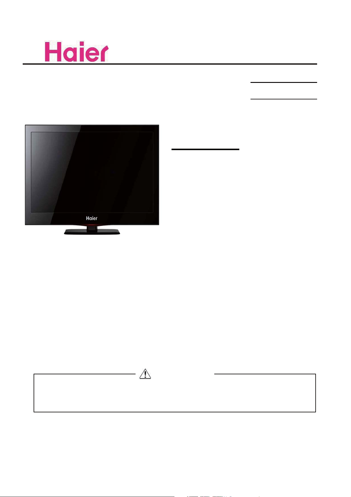
LED TV
Model No.
MSD308
LEY22T1000HF
Chassis
WARNING
This service information is designed for experienced repair technicians only and is not designed for use by the general public.
It does not contain warnings or cautions to advise non-technical individuals of potential dangers in attempting to service a product.
Products powered by electricity should be serviced or repaired only by experienced professional technicians. Any attempt to
service or repair the product or products dealt with in this service information by anyone else could result in serious injury
or death.
Page 2

Service Manual
Model No.:
Chapter 1: General Information
1-1. Table of Contents
1. General Information...........................................................................
1-1. Table of Contents
1-2. General Guidelines
1-3. Important Notice
1-4. How to Read this Service Manual
6SHFL¿FDWLRQV....................................................................................
3. Location of Controls and Components...........................................
3-1. Board Location
3-2. Main Board & AV Board
3-3. LCD Panel
4. Disassemble and Assemble..........................................................
4-1 Remove the Pedestal
4-2 Remove the Back Cover 12
4-3 Remove the Adhesive Tape 12
4-4 Remove the Main Board 13
1
1
3
3
6
6
88
8
8
10
12
12
4-5 Remove the Speaker 13
4-6 Remove the Remote Control Board 14
5. Installation Instructions..…....………………...........………….........
5-1 External Equipment Connections 15
5-2 HDMI Connections 18
6. Operation Instructions....…....………………...........………….........
6-1 Front Panel Controls
6-2 Back Panel Controls
6-3 Universal Remote Control
7. Electrical Parts…....………………...........………….........................
7-1. Block Diagram
7-2. Circuit Diagram
7-3. Wiring Connection Diagram
15
21
21
21
22
23
23
24
33
- 01 -
Page 3

Service Manual
Model No.:
8. Measurements and Adjustments........…………............................
8-1. How to enter into the factory model
8-2. How to update software
8-3. How to enter into the Hotel Model
9. Trouble-shooting…………..............................................................
9-1. Simple Check 48
9-2. Main Board Failure Check
9-3. Panel Failure
10. DVD OPERATION…………..............................................................
11. DVD Trouble shotting…………..............................................................
34
45
46
47
48
49
59
64
67
- 02 -
Page 4

Service Manual
Model No.:
1-2. General Guidelines
When servicing, observe the original lead dress. If a short circuit is found, replace all parts
which have been overheated or damaged by the short circuit.
After servicing, see to it that all the protective devices such as insulation barriers, insulation
papers shields are properly installed.
After servicing, make the following leakage current checks to prevent the customer from
being exposed to shock hazards.
1) Leakage Current Cold Check
2) Leakage Current Hot Check
3) Prevention of Electro Static Discharge (ESD) to Electrostatically Sensitive
1-3. Important Notice
1-3-1. Follow the regulations and warnings
Most important thing is to list up the potential hazard or risk for the service personnel to
open the units and disassemble the units. For example, we need to describe properly
how to avoid the possibility to get electrical shock from the live power supply or charged
electrical parts (even the power is off).
This symbol indicates that high voltage is present inside.It is dangerous to
make any king of contact with any inside part of this product.
This symbol indicates that there are important operating and maintenance
instructions in the literture accompanying the appliance.
1-3-2. Be careful to the electrical shock
7RSUHYHQWGDPDJHZKLFKPLJKWUHVXOW LQ HOHFWULFVKRFNRU¿UHGR QRW H[SRVHWKLV79VHW
to rain or excessive moisture. This TV must not be exposed to dripping or splashing water,
DQGREMHFWV¿OOHGZLWKOLTXLGVXFKDVYDVHVPXVWQRWEHSODFHGRQWRSRIRUDERYHWKH79
1-3-3. Electro static discharge (ESD)
Some semiconductor (solid state) devices can be damaged easily by static electricity. Such
components commonly are called Electrostatically Sensitive (ES) Devices. The following
techniques should be used to help reduce the incidence of component damage caused by
electros static discharge (ESD).
1-3-4. About lead free solder (PbF)
This product is manufactured using lead-free solder as a part of a movement within the
consumer products industry at large to be environmentally responsible. Lead-free solder
must be used in the servicing and repairing of this product.
8VHWKHJHQHZLQJSDUWVVSHFL¿HGSDUWV
Special parts which have purposes of fire retardant (resistors), high-quality sound
(capacitors), low noise (resistors), etc. are used.
When replacing any of components, be sure to use only manufacture's specified parts
shown in the parts list.
Safety Component
Ɣ&RPSRQHQWVLGHQWL¿HGE\PDUNKDYHVSHFLDOFKDUDFWHULVWLFVLPSRUWDQWIRUVDIHW\
- 03 -
Page 5

Service Manual
Model No.:
1-3-6 Safety Check after Repairment
&RQ¿UPWKDWWKHVFUHZVSDUWVDQGZLULQJZKLFKZHUHUHPRYHGLQRUGHUWRVHUYLFHDUHSXW
in the original positions, or whether there are the positions which are deteriorated around
the serviced places serviced or not. Check the insulation between the antenna terminal or
external metal and the AC cord plug blades. And be sure the safety of that.
General Servicing Precautions
1. Always unplug the receiver AC power cord from the AC power source before;
a. Removing or reinstalling any component, circuit board module or any other receiver
assembly.
b. Disconnecting or reconnecting any receiver electrical plug or other electrical
connection.
c. Connecting a test substitute in parallel with an electrolytic capacitor in the receiver.
CAUTION: A wrong part substitution or incorrect polarity installation of electrolytic
capacitors may result in an explosion hazard.
2. Test high voltage only by measuring it with an appropriate high voltage meter or other
voltage measuring device (DVM, FETVOM, etc) equipped with a suitable high voltage
probe.
Do not test high voltage by "drawing an arc".
3. Do not spray chemicals on or near this receiver or any of its assemblies.
4. Unless specified otherwise in this service manual, clean electrical contacts only by
applying the following mixture to the contacts with a pipe cleaner, cotton-tipped stick or
comparable non-abrasive applicator; 10% (by volume) Acetone and 90% (by volume)
isopropyl alcohol (90%-99% strength).
CAUTION:7KLVLVDÀDPPDEOHPL[WXUH
8QOHVVVSHFL¿HGRWKHUZLVHLQWKLVVHUYLFHPDQXDOOXEULFDWLRQRIFRQWDFWVLVQRWUHTXLUHG
Capacitors may result in an explosion hazard.
5. Do not defeat any plug/socket B+ voltage interlocks with which receivers covered by this
service manual might be equipped.
6. Do not apply AC power to this instrument and/or any of its electrical assemblies unless
all solid-state device heat sinks are correctly installed.
7. Always connect the test receiver ground lead to the receiver chassis ground before
connecting the test receiver positive lead.
Always remove the test receiver ground lead last. Capacitors may result in an explosion
hazard.
8VHZLWKWKLVUHFHLYHURQO\WKHWHVW¿[WXUHVVSHFL¿HGLQWKLVVHUYLFHPDQXDO
CAUTION: 'RQRWFRQQHFWWKHWHVW¿[WXUHJURXQGVWUDSWRDQ\KHDWVLQNLQWKLVUHFeiver.
9. Remove the antenna terminal on TV and turn on the TV.
10. Insulation resistance between the cord plug terminals and the eternal exposure metal
should be more than Mohm by using the 500V insulation resistance meter.
11. If the insulation resistance is less than M ohm, the inspection repair should be required.
If you have not the 500V insulation resistance meter, use a Tester. External exposure
metal: Antenna terminal Headphone jack
- 04 -
Page 6

Service Manual
Model No.:
Electrostatically Sensitive (ES) Devices
Some semiconductor (solid-state) devices can be damaged easily by static electricity.
Such components commonly are called Electrostatically Sensitive (ES) Devices.
Examples of typical ES devices are integrated circuits and some field-effect transistors
and semiconductor "chip" components. The following techniques should be used to help
reduce the ncidence of component damage caused by static by static electricity.
1. Immediately before handling any semiconductor component or semiconductorequipped assembly, drain off any electrostatic charge on your body by touching a known
earth ground. Alternatively, obtain and wear a commercially available discharging wrist
strap device, which should be removed to prevent potential shock reasons prior to applying
power to the unit under test.
2. After removing an electrical assembly equipped with ES devices, place the assembly
on a conductive surface such as aluminum foil, to prevent electrostatic charge buildup or
exposure of the assembly.
3. Use only a grounded-tip soldering iron to solder or unsolder ES devices.
4. Use only an anti-static type solder removal device. Some solder removal devices not
FODVVL¿HGDVDQWLVWDWLFFDQJHQHUDWHHOHFWULFDOFKDUJHVVXI¿FLHQWWRGDPDJH(6GHYLFHV
'RQRWXVHIUHRQSURSHOOHGFKHPLFDOV7KHVHFDQJHQHUDWHHOHFWULFDOFKDUJHVVXI¿FLHQW
to damage ES devices.
6. Do not remove a replacement ES device from its protective package until immediately
before you are ready to install it.
(Most replacement ES devices are packaged with leads electrically shorted together by
conductive foam, aluminum foil or comparable conductive material).
7. Immediately before removing the protective material from the leads of a replacement
ES device, touch the protective material to the chassis or circuit assembly into which the
device will be installed.
CAUTION: Be sure no power is applied to the chassis or circuit, and observe all other
safety precautions.
8. Minimize bodily motions when handling unpackaged replacement ES devices.
(Otherwise harmless motion such as the brushing together of your clothes fabric or the
OLIWLQJRI\RXUIRRWIURPDFDUSHWHGÀRRUFDQJHQHUDWHVWDWLFHOHFWULFLW\VXI¿FLHQWWRGDPDJH
an ES device.)
1-3-7. Ordering Spare Parts
Please include the following informations when you order parts. (Particularly the Version
letter)
1. Model number, Serial number and Software Version
The model number and Serial number can be found on the back of each product and the
Software Version can be found at the Spare Parts List.
2. Spare Part No. and Description
<RXFDQ¿QGWKHPLQWKH6SDUH3DUWV/LVW
- 05 -
Page 7

1-3-8. Photo used in this manual
The illustration and photos used in this Manual may not base on the final design of
products, which may differ from your products in some way.
1-4. How to Read this Service Manual
Using Icons:
,FRQVDUHXVHGWRDWWUDFWWKHDWWHQWLRQRIWKHUHDGHUWRVSHFL¿FLQIRUPDWLRQ7KHPHDQLQJRI
each icon is described in the table below:
Note:
A “note” provides information that is not indispensable, but may nevertheless be valuable
to the reader, such as tips and tricks.
Service Manual
Model No.:
Caution:
A “caution” is used when there is danger that the reader, through incorrect manipulation,
may damage equipment, loose data, get an unexpected result or has to restart(part of) a
procedure.
Warning:
A “warning” is used when there is danger of personal injury.
Reference:
A “reference” guides the reader to other places in this binder or in this manual, where he/
VKHZLOO¿QGDGGLWLRQDOLQIRUPDWLRQRQDVSHFL¿FWRSLF
- 06 -
Page 8
Service Manual
Model No.:
6SHFL¿FDWLRQV
Model LEY22T1000HF
Screen Size 21.5 inch
Aspect Ratio 16:9
Resolution 1920*1080
Response Time (ms)
Angel of View 176o
Color Display16.7M
5.0 (GRAY TO
GRAY)
No. of Preset Channels 1000
OSD LanguageEnglish
Color System PAL/SECAM
Audio System DK, BG, I, M, L, L'
Audio Output Power
3W×2
(Built-in) (W)
Audio Output Power
No
(outer) (W)
Tot al Power Input (W) 38W
Voltag
Power Frequency (Hz) 50~60Hz
Net Weight (KG) 3.35
Gross Weight (KG) 3.8
e Range (V)
AC 100-240V
Net Dimension (MM) 518.5*322*50
Packaged Dimension
518.5*363*160
(MM)
- 07 -
Page 9
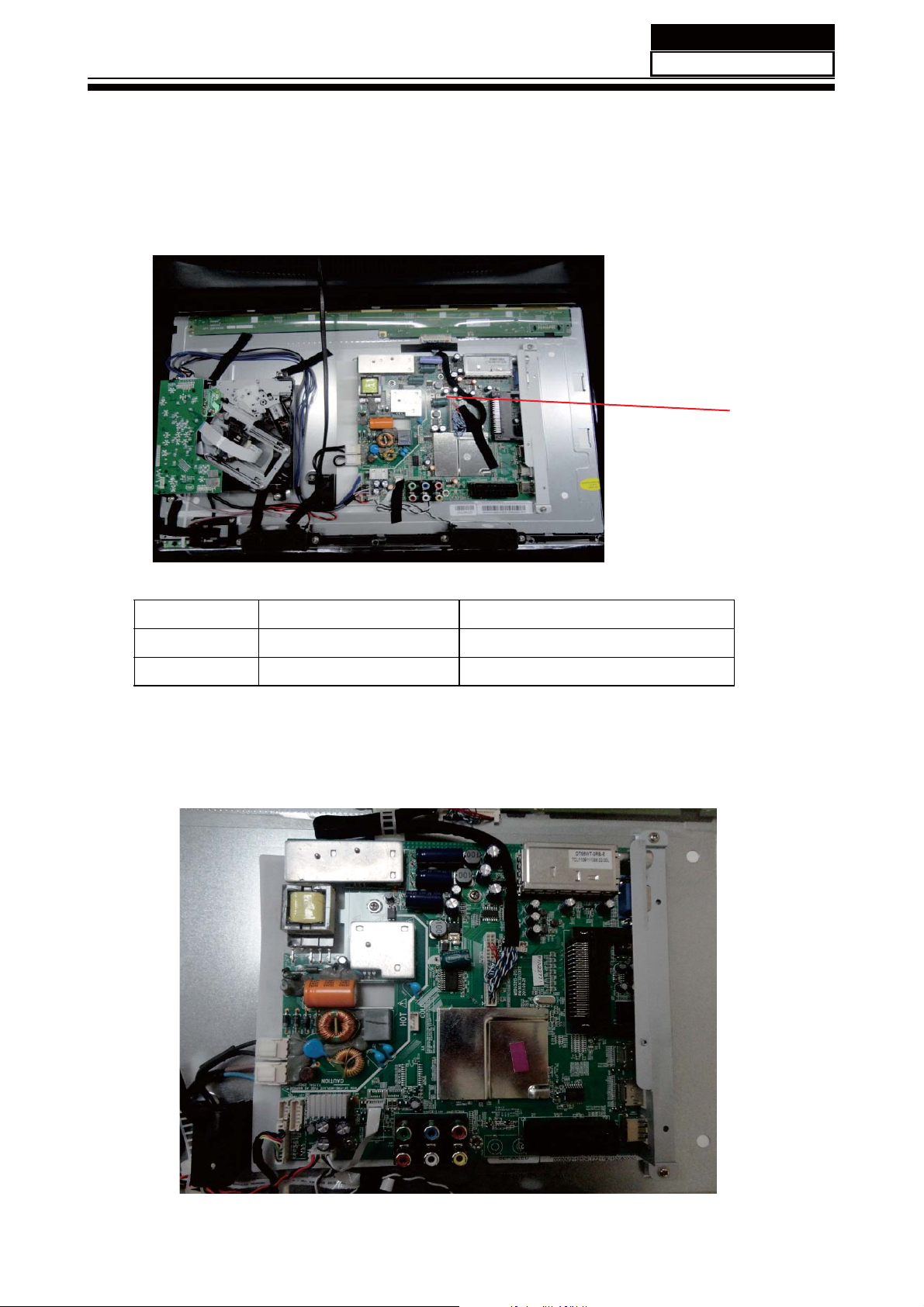
3. Location of Controls and Components
3-1 Board Location
Service Manual
Model No.:
A Board
No. Description
A Board Integration Mainboard
3-2 Main Board
DH1Q00M0600M
- 08 -
Page 10
Service Manual
Model No.:
3-2-1 Function Description:
Main Board
Process signal which incept from exterior equipment then translate into signal that panel
can display.
&RQQHFWRUGH¿QLWLRQ
Main board connector
Keypad andremote connector (CN8)
3LQQXPEHU 6LJQDOQDPH 'HVFULSWLRQ
/('B*
7
8
9
10
/('B5
STANDBY
,5 5(027(&21752/
*1'
9
NC
.(<
.(<
*1'
/$035('
/$03*5((1
*1'
32:(5)255(027(
Speaker connector (CN30)
Pin number Signal name Description
1 RSPK+ RSPK+
2 RSPK- RSPK3 LSPK- LSPK4 LSPK+ LSPK+
- 09 -
Page 11
3-3. LED Panel
Service Manual
Model No.:
MTC215LED-P07H(CLAB215FA04 V4)
- 10 -
Page 12

Service Manual
Model No.:
3-4-1.Connector de finition
PIN NO. REMARK FUNCTION
1 RXO0- minus signal of odd channel 0(LVDS)
2 RXO0+ plus signal of odd channel 0(LVDS)
3 RXO1- minus signal of odd channel 1(LVDS)
4 RXO1+ plus signal of odd channel 1(LVDS)
5 RXO2- minus signal of odd channel 2(LVDS)
6 RXO2+ plus signal of odd channel 2(LVDS)
7 GND GND
8 RXOC- minus signal of odd clock channel (LVDS)
9 RXOC+ plus signal of odd clock channel (LVDS)
10 RXO3- minus signal of odd channel 3(LVDS)
11 RXO3+ plus signal of odd channel 3(LVDS)
12 RXE0- minus signal of even channel 0(LVDS)
13 RXE0+ plus signal of even channel 0(LVDS)
14 GND GND
15 RXE1- minus signal of even channel 1(LVDS)
16 RXE1+ plus signal of even channel 1(LVDS)
17 GND GND
18 RXE2- minus signal of even channel 2(LVDS)
19 RXE2+ plus signal of even channel 2(LVDS)
20 RXEC- minus signal of even clock channel (LVDS)
21 RXEC+ plus signal of even clock channel (LVDS)
22 RXE3- minus signal of even channel 3(LVDS)
23 RXE3+ plus signal of even channel 3(LVDS)
24 GND GND
25 NC NC
26 NC Test pin (Can’t connect to GND)
27 NC NC
28 VCC Power supply input voltage(5.0 V)
29 VCC Power supply input voltage(5.0 V)
30 VCC Power supply input voltage(5.0 V)
1) Keep the NC Pin and don’t connect it to GND or other signals.
2) GND Pin must connect to the ground, don’t let it be a vacant pin.
- 11 -
Page 13
Service Manual
Model No.:
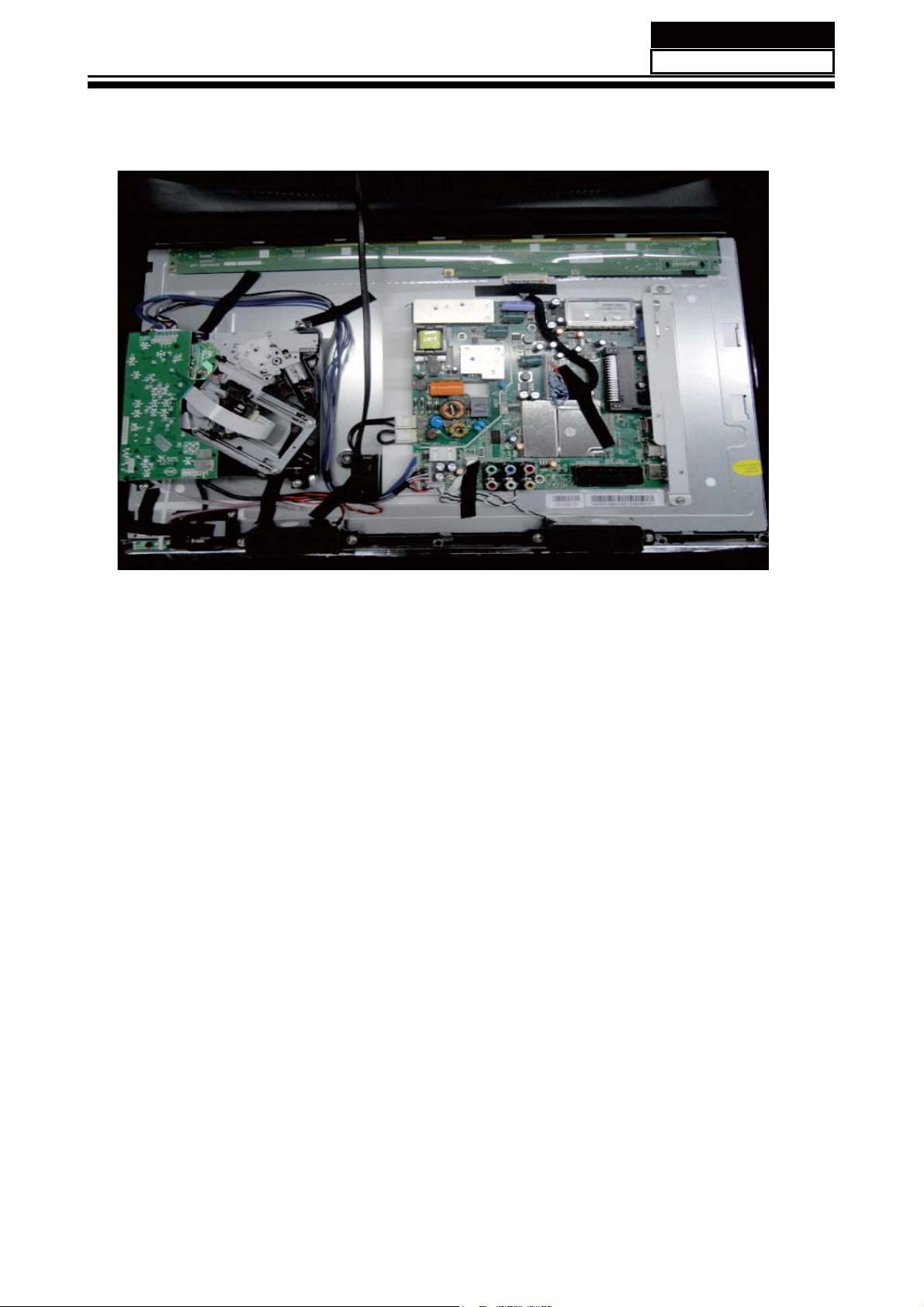
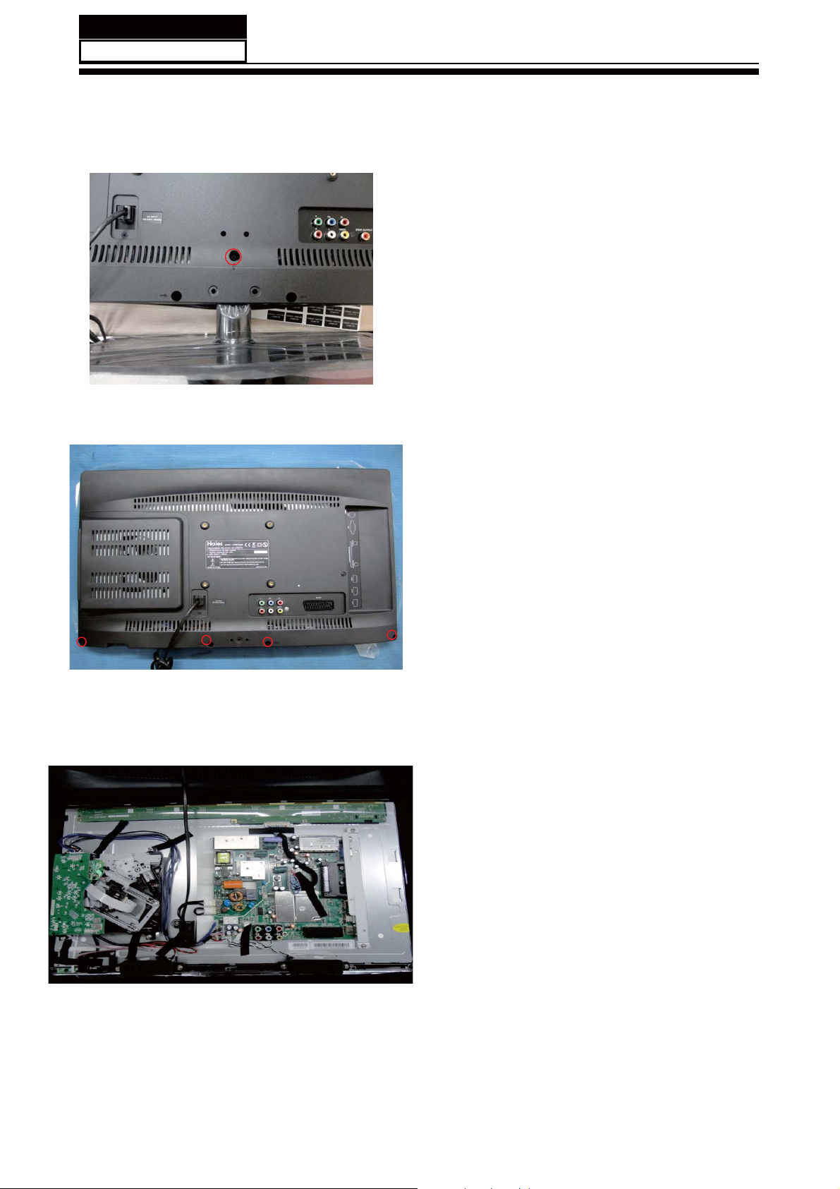
4. Disassemble and assemble
4-1 Remove the Pedestal
4-2Remove the Back Cover
/D\GRZQWKHXQLWVRWKDWUHDUFRYHU
faces upward
5HPRYH WKHWKUHH VFUHZIURPWKH
UHDUFRYHULQGLFDWHGZLWKż
7KHQUHPRYHWKHSHGHVWDO
4-3. Remove the adhesive tape
5HPRYHWKHWKHVHVFUHZLQGLFDWHGRQ
¿JXUHDERYHE\ż
7KHQUHPRYHWKH EDFNFRYHUIURP WKH
unit.
Remove the adhesive tape indicated on the
¿JXUHDERYH
- 12 -
Page 14
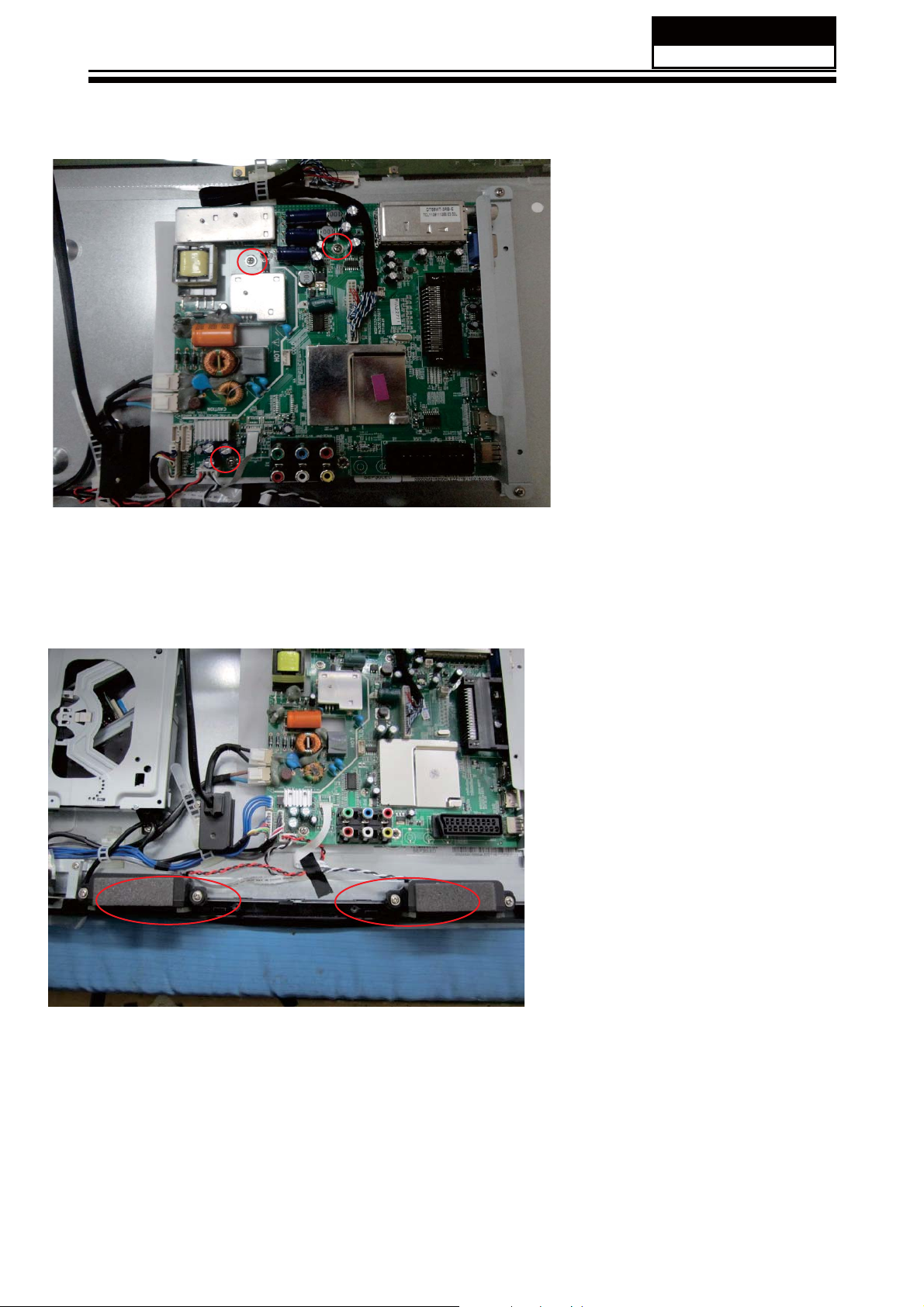
4-4 Remove the Main board
Service Manual
Model No.:
'LVFRQQHFWHG WKHFRXSOHU
CN5
5HPRYHWKH0DLQERDUG
CN8
CN800
CN19
CN30 CN804
CN805
CN18
4-5 Remove the speaker
Take out the speaker
- 13 -
Page 15
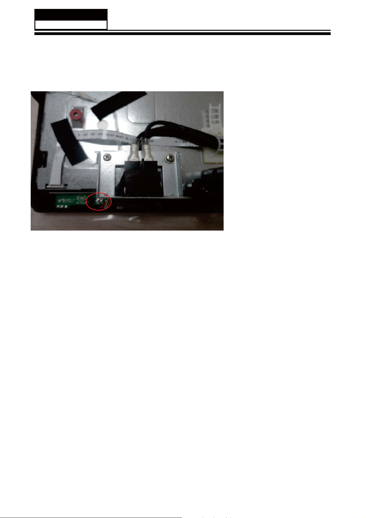
Service Manual
Model No.:
4-6 Remove the remote control
take out the remote control
board
- 14 -
Page 16
5. Installation Instructions
5-1 External Equipment Connections
Accessories
Service Manual
Model No.:
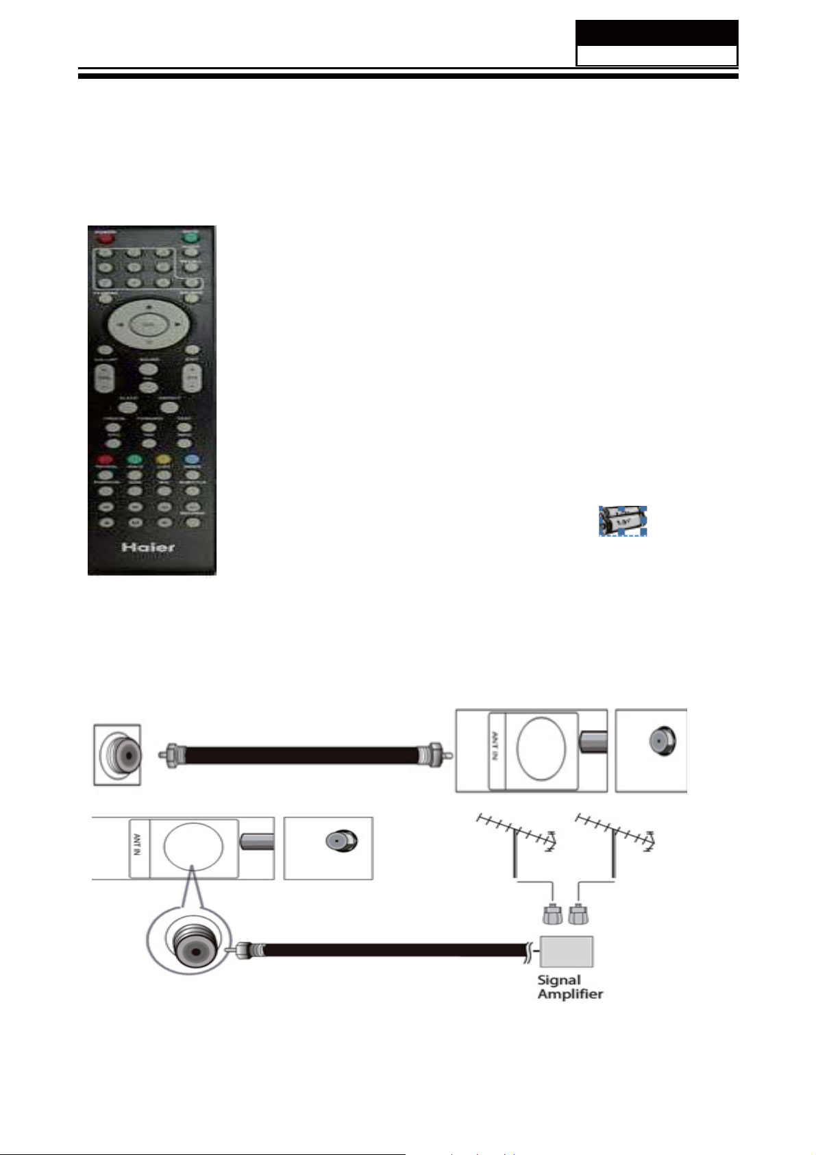
Remote Control
Antenna Connection
Connect one end of a coaxial cable (not included) to the ANT IN jack on the back of
your TV/DVD combo, then connect the other end of the cable into the antenna or cable
TV wall outlet.
User GUIDE
Battery
To improve picture quality from an antenna in a poor signal area, install a signal
DPSOL¿HU
If you need to split the antenna signal to connect two TVs, install a two-way splitter.
- 15 -
Page 17
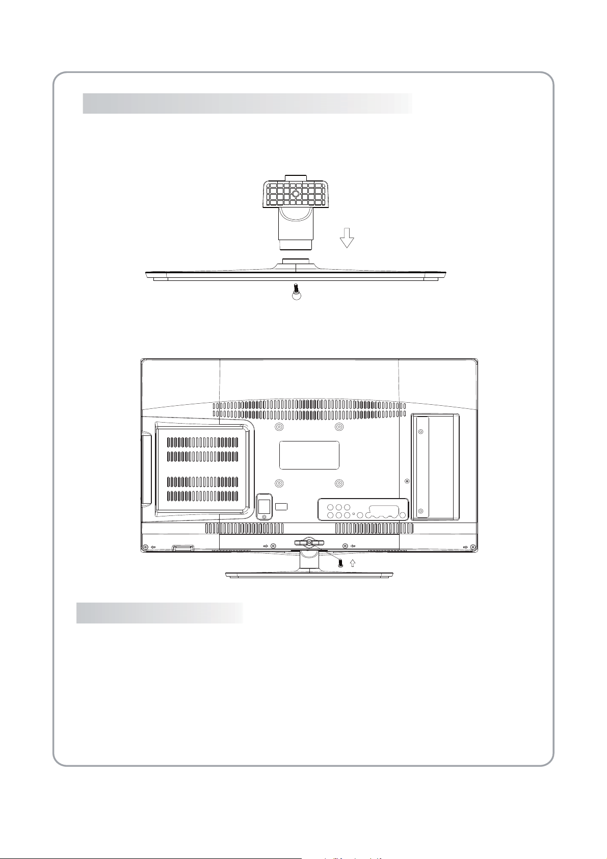
Base Stand Assembly Instruction
19"/22"/24"
1. Insert the stand support pillar into the stand as the arrow indicated
direction, and then fastened with one screw.
2. Insert the stand Ass'y into back cover as the arrow indicated direction,
and then fastened with one screw.
INSTALLATION NOTES
Locate the TV in a room where light does not strike the screen directly. Total darkness or a reflection on the screen
can cause eyestrain. Soft and indirect lighting is recommended for comfortable viewing.
Allow enough space between the TV and the wall to permit ventilation.
Please don’t rotate the TV!
Avoid excessively warm locations to prevent possible damage to the cabinet or premature component failure.
- 16 -
Page 18
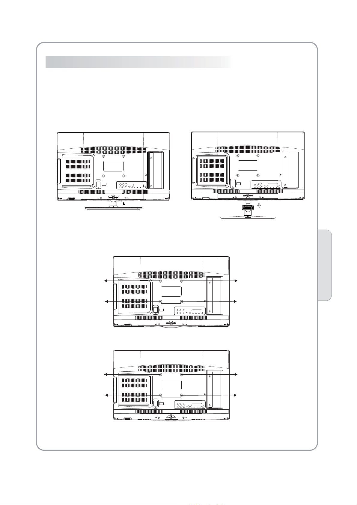
WALL MOUNTING INSTALLATION GUIDELINES
This television can be wall mounted as follows:
1.Place the LED LCD Television onto a solid surface. Please place some soft material
over the front of the screen to protect it from any damage.
2.Remove the screws from the lower part of the television, where the base joins to the
TV, and take away the stand (put the stand somewhere safe for future use).
19"/22"/24"
M4X5
M4X5
M4X5
M4X5
75mm
75mm
(19")
100mm
100mm
(22",24")
M4X5
M4X5
M4X5
M4X5
Introduction
02
- 17 -
Page 19

Service Manual
Model No.:
5-2 HDMI Connections
When the source device(DVD player or Set Top Box) supports HDM
How To Connect
1. Connect the source device to HDMI port of this TV with an HDMI cable(not supplied
with this product).
2. No separated audio connection is necessary.
How To Use
If the source device supports Auto HDMI function, the output resolution of the source
device will be automatically
set to 1280x720p.
If the source device does not support Auto HDMI, you need to set the output resolution
appropriately.
To get the best picture quality, adjust the output resolution of the source device to
1280x720p.
Select HDMI input source in input source option of Select Main source menu.
When the source device(DVD player or Set Top Box) supports DVI
How To Connect
1. Connect the source device to HDMI port of this TV with a HDMI-to-DVI cable(not
supplied with this product).
2. A separated audio connection is necessary.
3. If the source device has an analog audio output connector, connect the source device
audio output to DVI Audio In port located on the PC port.
How To Use
If the source device supports Auto DVI function, the output resolution of the source device
will be automatically
set to 1280x720p.
If the source device does not support Auto DVI, you need to set the output resolution
appropriately.
To get the best picture quality, adjust the output resolution of the source device to
1280x720p.
Press the INPUT button to select HDMI input source in input source option of Select Main
source menu.
Installation
- 18 -
Page 20
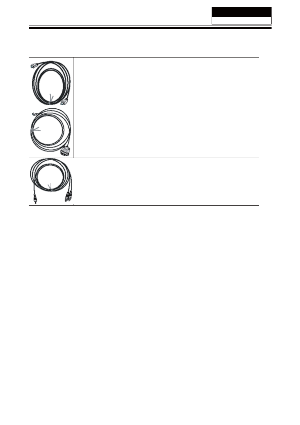
Cable sample
Service Manual
Model No.:
HDMI Cable
(not supplied with the product)
HDMI to DVI Cable
( not supplied with the product)
Analog Audio Cable
(Stereo to RCA type)
(not supplied with the product)
-19 -
Page 21
Service Manual
Model No.:
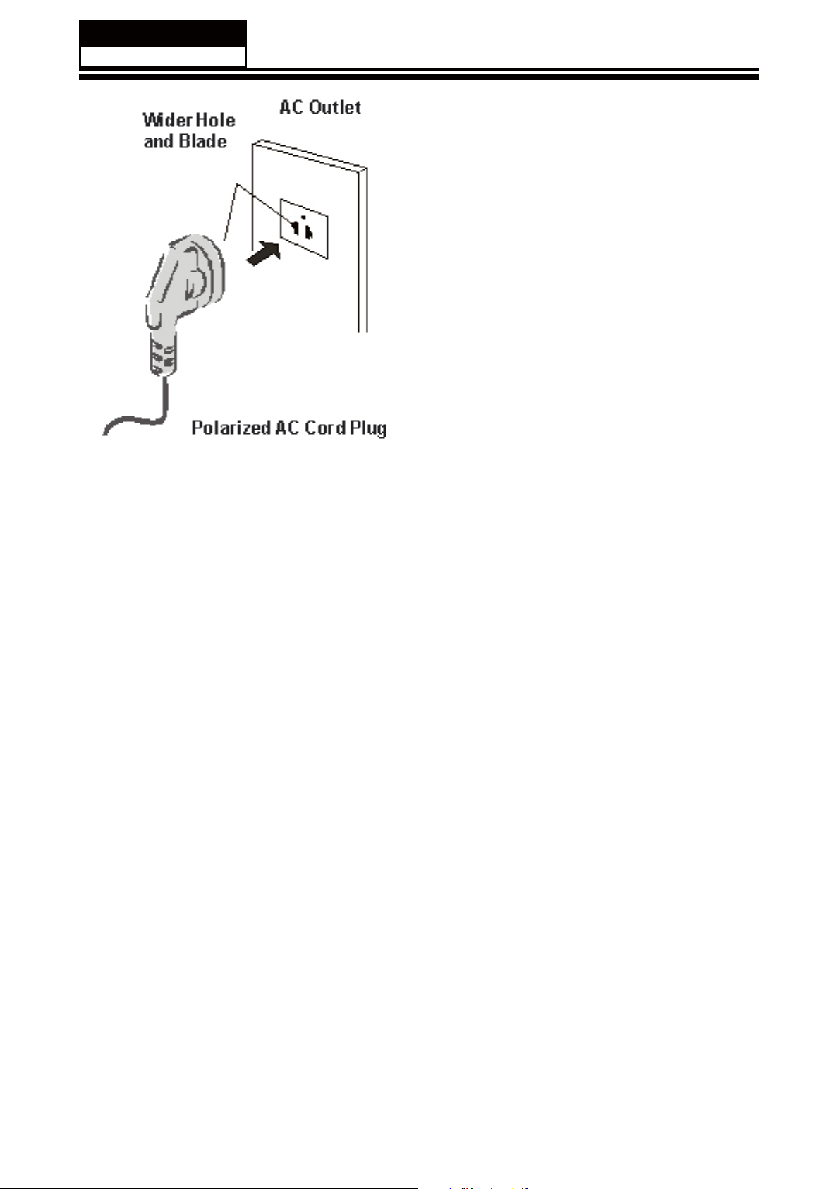
Power source
TO USE AC POWER SOURCE
Use the AC polarized line cord provided for operation on AC.
Insert the AC cord plug into a standard polarized AC outlet.
NOTES:
Ŷ1HYHUFRQQHFWWKH$&OLQHFRUGSOXJWRRWKHUWKDQWKHVSHFL¿HGYROWDJH
Use the attached power cord only.
Ŷ,IWKHSRODUL]HG$&FRUGGRHVQRW¿WLQWRDQRQSRODUL]HG$&RXWOHW
GRQRWDWWHPSWWR¿OHRUFXWWKHEODGH,WLVWKHXVHUCVUHVSRQVLELOLW\WRKDYHDQ
electrician replace the obsolete outlet.
Ŷ ,I \RXFDXVH DVWDWLF GLVFKDUJHZKHQWRXFKLQJ WKHXQLW DQGWKH XQLWIDLOV WRIXQFWLRQ
simply unplug the unit from the AC outlet and plug it back in. The unit should return to
normal operation.
- 20 -
Page 22
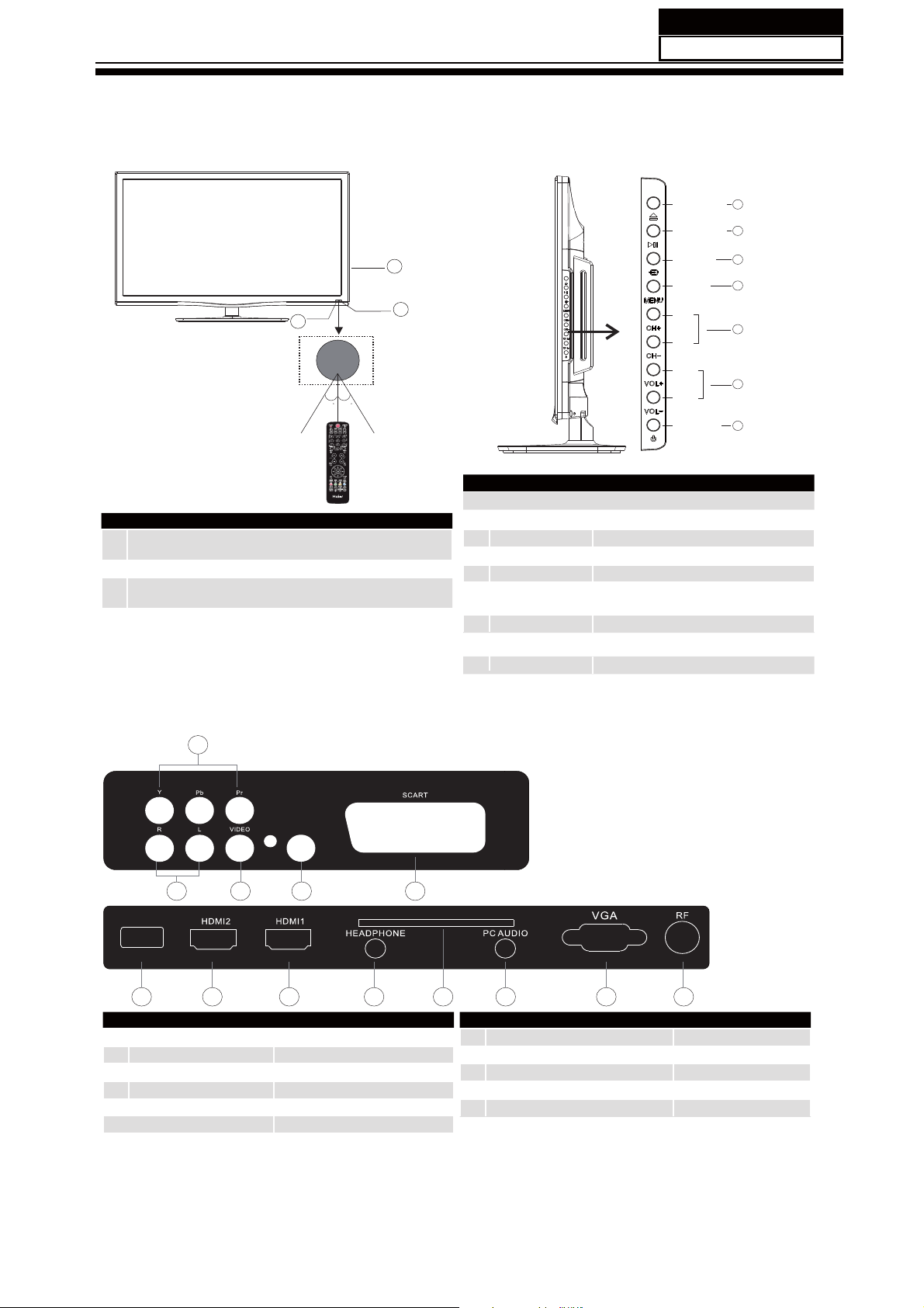
6. Operation Instructions
6-1 Front panel controls
Service Manual
Model No.:
1
Remote control sensor.
Indicator LED:
2
BLUE: POWER ON. RED: STAND BY.
Key board.
3
OPEN/CLOSE
PLAY/PAUSE
3
2
30 30
1
OPEN/CLOSE
1
PLAY/PAUSE
2
3
4
5
6
SOURCE
MENU
CH+/CH-
VOL+/VOL-
Display the input source menu.
Display main MENU.
In TV mode,press CH+ or CH- to change
the channel up and down.
In MENU, press CH+ or CH- to select items .
Adjust sound level.
SOURCE
MENU
CH+
CH-
VOL+
VOL-
STANDBY
1
2
3
4
5
6
7
In MENU,adjust the item that you Selected.
6.2 Back panel controls
4
SPDIF OUTPUT
3
input
input
digital audio output
input
input
input
input
1
2
3
4
5
6
7
USB
6
L/R AUDIO
VIDEO
S/PDIF
YPbPr
SCART
USB
HDMI2
1 2
7 8 9 10
7
5
COMMON INTERFACE (CI)
8
9
10
11
12
13
STANDBY
11 12 13
HDMI1 input
HEADPHONE
COMMON INTERFACE(CI)
PC AUDIO
VGA
RF
analogue audio output
input
input
input
input
- 21 -
Page 23

Service Manual
Model No.:
6-3 Setting Up Your Remote Control
1.POWER:
3.P.Mode:
4.INFO:
source and channel audio mode.
5.AUDIO I/II: MONO,Nicam stereo
channel. Select Audio language for DTV channel.
6.SUBTITLE: On Off
7.Number Buttons:
8.SOURCE:
9.MUTE:
10.Volume Control:
11.MENU:
12.OK:
13.EXIT:
14.Teletext Index/USB PLAY
16.Teletext Green Button / USB Fast Forward
17.
18.Teletext Mix
19.Teletext Text
20.Teletext Reveal
21.Teletext Size
22.Teletext Time/ANGLE/REC.LIST
23.Teletext Mode:
24.Teletext Hold
25.Teletext Subcode:Teletext Subpage
26.Teletext Blue Button / USB Next File
27.Teletext Yellow Button / USB Previous File
28.USB STOP
29.USB PAUSE
30.START RECORD
31.UP,DOWN,LEFT,RIGHT Cursor:
selection.
32.Fav:
33.Select Programme:
previous TV channel.
34.GUIDE:
mode.
35.Q.View:
36.CH.LIST:
37.Screen:
38.Sleep :
39.S.Mode:
Press to turn on the TV.
To switch picture mode.
Press to display the current signal status,including input
Press to select for ATV
Press to turn the subtitle or .
For direct access to channels.
To select input source.
To disable or enable the sound output.
To adjust sound level.
To display TV menu.
To confirm selection.
To return to the previous menu or exit menu.
Teletext Red Button / USB Fast Rewind
(teletext time is no function)
No function
Press to navigate your
To access your favourite channels list in TV or DTV mode.
Press / Button to select the next or
Press to display electronic programme guide in TV
To access the previously viewed channel.
Press to display the channel list.
To change picture aspect ratio.
Set ti me r to t urn off the TV.
To switch sound mode.
Remote Control
03
- 22 -
Page 24

Remote Control - DVD section
2.D.MENU:
menu.
5.AUDIO:
6.SUBTITLE:
from disc).
7. :Press to set the time, select title, chapter or track
Numeric keys
you wish to play. Press the ENTER/OK Button to confirm. When a
VCD is playing (with PBC off), press the Numeric keys to select a
track directly.
12. :Press to confirm.
14. :
15. :Press to select between different repeat modes -Repeat
Chapter / Repeat Title / Repeat Off(for DVD discs),Repeat Single/
Repeat Folder/All/ Repeat
Off(for VCD/CD/MP3 discs).
16. :Press to fast-forward play in DVD, CD MP3 or VCD
mode.Press repeatedly to scroll through fast-forward speeds. Press
the Play/Pause Button to resume play
17. :Press to rewind play in DVD, CD MP3 or VCD mode. Press
repeatedly to scroll through rewind speeds. Press the Play/Pause
Button to resume play.
18. :Press to display the DVD Main M enu.
19. :Press to enter the system setting menu. Press again
to exit the menu.
20. :Programe the DVD.
21. :Press to repeat a segment of the disc you are watching
between A and B. (DVD mode)
22. :Press to view scenes shot from different angles. (Disc
support is required)
23. :Press to show the information of the current playing disc.
24. :No function.
25. :For DVD discs, press to choose the desired title and
chapter and search the desired title, time and chapter time. For Super
VCD,VCD,CD discs, press this button to search the desired disc time
and track time and choose the desired track.
Note
26. :During DVD,CD,MP3, or VCD playback, press to play
the next chapter, title or track.
27. :During DVD, CD,M P3, or VCD playback, press to
play the previous chapter, title or track.
28. :Press to stop play of the DVD you are watching at anytime.
29. :Press to pause play of the DVD of media.
35. :
40. :To open the disc, press OPEN / CLOSE;To close
the disc, press OPEN/CLOSE again.
During DVD playback, press MENU to display the disc
Changes the audio language or audio channel.
Press to choose different captions (Requires support
OK
Press to begin play of the DVD of media you wish to view.
PLAY
REPEAT
FWD
REV
TITLE
DVD SE TU P
PROGRAME
A-B
ANGLE
D.CALL
10+
SEARCH
: During VCD playback, the PBC mode must be set to OFF.
NEXT NEXT
PREV PREV
STOP
PAUSE
Press to return to the Main Menu.
Q.View
OPEN/CLOSE
- 23 -
Page 25

REMOTE CONTROL
TELETEXT
Teletext is an information system broadcast by certain channels which can be consulted like a newspaper. It also
offers access to subtitles for viewers with hearing problems or who are not familiar with the transmission
language(cable networks, satellite channels, etc.)
Press:
T
EXT
SELECTING A PAGE
DIRECT ACCESS
TO THE ITEMS
INDEX
SUB PAGE
HOLD
You will obtain:
This is used to call or exit teletext modes. The summary appears with a list of items that can be
accessed. Each item has a corresponding 3 digit page number. If the channel selected does
not broadcast teletext, theindication 100 will be displayed and the screen will remain blank (in
this case, exit teletext and select another channel).
Enter the number of the page required using the 0 to 9 up/down. Example: page 120, enter 120.
The number is displayed top left, the counter turns and then the page is displayed. Repeat this
operation to view another page. If the counter continues to search, this means that the page is
not transmitted. Select another number.
Coloured are as are displayed at the bottom of the screen. The 4 coloured keys are used to
access the items or corresponding pages. The coloured areas flash when the item or the page
is not yet available.
This returns to the contents page (usually page 100).
Certain pages contain sub-pages which are automatically displayed successively. This
key is used to stop or resume sub-page acquisition. The indication appears top left.
E
To freeze the page.
REVEAL
LIST
To display or hide the concealed information (games solutions).
The user can set four favorite pages to be directly linked to the four color keys. While list mode
is activated, it is not possibility to use TOP or FLOF navigation with the colorkeys. The favorite
page numbers should be stored and restored to/from nonvolatile memory for each channel by
the system software.
Page 26

4
7. Electrical parts
7-1. Block diagram
Service Manual
Model No.:
1
+5V
+5VSTB
+12V
TITLE:
⧚Ḛ
DWG NO:
VER:A
1
POWER
MODEL:
PART NO.:
SHEET: OF
SHEN ZHEN AMTC MULTIMEDIA CO.,LTD
AC INPUT
2
EARPHONE output
TDA1517 2X3W output
MUTE TDA1517
DF3544
3
AUDIO
MUTE 3544
OFF
ON
OFF
ON
SC1_FS
DVD_ON/OFF
ON_PANEL
Y8
E4
AA7
ON_PBACK
PANEL-ADJ-PWM
LCD_OP
F4
E6
R6
FLASH
DDR2
DESIGN:
DDR2
ᓴ҂
CHECKED:
APPRD:
PANEL
2
3
GPIO1(C7)
LINEOUT3(AA6\Y5)
MSD309PX
MSD308PX
TS1
TS0
4
GPIO0(A7)
LINEIN5(AD6\ADC)
CVBS4(W2)
RGB2
RGB0
SCH BLOCK FOR MSD308/309PX
TS Stream to 309
Encrypt TS Stream to CI
CI CARD
HDMI1 Input
AIF for analog TV
DIF for DTV
5
OPTION
Rear CVBS input
YPbPr input
HDMI2 Input
TUNER
Schematics Blockdiagram
D D
C C
PC RGB input
Rear audio input
ON
LINEOUT3(AA6\Y5)
CVBS_OUT(V3)
LINEIN1(T6\U6)
CVBS0(AC5)
RGB1
LINEIN2(V6/U5)
PC audio input
SCART RGB input
SCART CVBS input
SCART audio input
SCART CVBS output
SCART audio output
B B
OFF
GPIO4(C3)
PO(B1\C2)
USB1 POWER CONTROL
USB1 DATA
CVBS2(W5)
DVD CVBS input
LINEIN0(R4\R5)
4
DVD audio
5
A A
- 23 -
Page 27

5
ᇚ
ᦤ催䕏䕑ᬜ⥛ˈ
ⳕ⬉خࠄ
ҹϟDŽ
D803
D803
2A06
2A06
D807
D807
2A06
2A06
R883
R883
1M/1206
1M/1206
R885
R885
1M/1206
1M/1206
D D
CY800CY800
S3S3
18.5ᇌ㟇24
26
R850
LED1
LED2
LED3
LED4
C C
26
ᇌՓ⫼0Rˈ݊ᅗሎᇌ㾚⬉⌕㗠ᅮ
LED1
LED3
LED9 ON/BK
LED10
LED11
LED12
12VA
B B
+
+
EC800
EC800
0.1uF
0.1uF
C800
C800
220uF/16V
220uF/16V
MST Power supply
45mA
5Vstb
10uF(X5R)
10uF(X5R)
D804
D804
2A06
2A06
D805
D805
2A06
2A06
34
LF801LF801
R876
R876
12
470K/1206
470K/1206
CX1CX1
R886
R886
R884
R884
NC/24K-1206
NC/24K-1206
1M/1206
1M/1206
R888
R888
1M/1206
1M/1206
CY801CY801
34
LF800LF800
C1068
C1068
12
RV1
RV1
PTC
PTC
RDH5-3A-W
RDH5-3A-W
F800F800
S4S4
S5S5
S2S2
1
2
1
2
CN800
CN800
CN805SWCN805
AC IN
AC IN
SW
ᇌѠᦦՓ⫼U5ˈ䕃ᥦ㒓ⱘՓ⫼
ᇌՓ⫼ϝ乫偅ࡼ
ˈՓ⫼Ѡᦦᯊˈ䌈Ϟˈ݊ᅗ⢊ᗕᯊϡ䳔㽕䌈
R832
R832
100R
1
CH1
2
CH2
3
CH3
4
CH4
5
PGND1
6
PGND2
7
LED5
CH5
8
LED6
AP3608EU3AP3608E
CH6
9
LED7
CH7
LED8
CH810PWM
NC
R834NCR834
LED2
R836NCR836
LED4
NC
U4
1
CH1
2
CH2
3
CH3
4
CH4
5
PGND1
6
PGND2
7
LED13
CH5
8
LED14
CH6
9
LED15
CH7
LED16
CH810PWM
L800 10uH_1.5AL800 10uH_1.5A
+
+
C948
C948
C949
C949
220uF/16V
220uF/16V
V =0.6X(1+R /R )
FB8
FB8
10uH_1.5A
10uH_1.5A
C920
C920
C965
C965
0.1uF(X7R)
0.1uF(X7R)
100R
20
EN
19
VCC
18
AGND
17
SDBXSDBX
SDBX
16
SHD
SDB
R830
R830
15
FB
20K
20K
14
U3
ISET
R828
R828
13
FBX
FBX
12
12K
12K
NC
11
R76
R76
100R
100R
BL-ADJUST
R835NCR835
LED5
LED6
NC
R837NCR837
LED7
LED8
NC
R838
R838
100R
100R
20
AP3608EU4AP3608E
EN
19
VCC
18
AGND
17
SDBX
16
SDBX
SDB
15
FBX
FB
14
ISET
R841
R841
13
FBX
12K
12K
12
NC
11
R853
R853
100R
100R
BL-ADJUST
U800
U800
SY8101B
SY8101B
BS
5
VIN
LX
R802
R802
SY8101B
SY8101B
10K
10K
SOT23-6
SOT23-6
4
EN
FB
GND
2
0.1uF(X7R)
0.1uF(X7R)
up
out
U803
U803
B
⠜ࡴ
AIC2352
AIC2352
4
AIC2352
AIC2352
R8681KR868
SOT-23
SOT-23
1K
1
OUT/FB5EN
GND
2
R877
R877
470k/1206
470k/1206
102/25V/0805
102/25V/0805
S1S1
R831
R831
51K
51K
CERAMIC
1
6
3
down
LX3VIN
Vout =0.6X(1+(R855+R857)/R859)
4
1
U804
U804
SY8008B SOT-23
SY8008B SOT-23
AIC2354
AIC2354
SOT-23
SOT-23
GND
2
680mA
L804
L804
2.2uH_1.5A
2.2uH_1.5A
R816
R816
120K
120K
LX3VIN
R817
R817
82K
82K
OUT/FB5EN
R818
R818
100K
100K
5VA
FB6
FB6
10uH_1.5A
10uH_1.5A
C1002
C1002
A A
0.1uF(X7R)
0.1uF(X7R)
R8151KR815
C1001
C1001
1K
10uF(X5R)
10uF(X5R)
C1000
C1000
10uF(X5R)
10uF(X5R)
C1012
C1012
100PF
100PF
5
EC805
EC805
+
+
47uF/400V
47uF/400V
C1056
C1056
0.1uF-50V-K-0805(X7R)
0.1uF-50V-K-0805(X7R)
R878
R878
470k/1206
470k/1206
U807U807
5
3
VDD
RI
6
GATE
4
CS
2
FB
GND
1
U5+U3
ON/BK
+5V
C15 1uF-0603C15 1uF-0603
0.1uF(X7R)
0.1uF(X7R)
C18
C18
FB
R829NCR829
NC
21.5"R828䌈15K
23.6/26"R828,R841
R850
R850
+5V
100R-0603
100R-0603
Փ⫼
CN2
+5V
C16 1uF-0603C16 1uF-0603
0.1uF(X7R)
0.1uF(X7R)
C20
C20
R842NCR842
NC
C943
C943
0.1uF(X7R)
0.1uF(X7R)
L803
L803
10uH_1.5A
10uH_1.5A
C950
C950
33P
33P
R800
R800
150K
150K
R806
R806
20K
20K
3.3VU 3.3VU
L808
L808
2.2uH_1.5A
2.2uH_1.5A
R855
R855
120K
120K
C966
C966
33P
33P
R857
R857
330K
330K
R859
R859
100K
100K
LDOᬍЎDC to DC,
1.8VA
1.812V
1.8VA
Vpp=23mV
C99933P/NC C99933P/NC
C1 10uF(X5R)C1 10uF(X5R)
C2 10uF(X5R)C2 10uF(X5R)
1.8VA
4
+
+
47uF/50V
47uF/50V
C1053
C1053
B
⠜ࡴ
+12V
1uF-0603
1uF-0603
䌈
SHD
ᯊˈ䌈Ϟ
BL-ADJUST
LED9
LED13
218mA
C951
C951
C952
C952
10uF(X5R)
10uF(X5R)
10uF(X5R)
10uF(X5R)
C967 10uF(X5R)C967 10uF(X5R)
0.3W
C985 0.1uF(X7R)C985 0.1uF(X7R)
C986 0.1uF(X7R)C986 0.1uF(X7R)
C987 10uF(X5R)C987 10uF(X5R)
C988 10uF(X5R)C988 10uF(X5R)
C989 10uF(X5R)C989 10uF(X5R)
C990 10uF(X5R)C990 10uF(X5R)
C991 10uF(X5R)C991 10uF(X5R)
C399 0.1uF(X7R)C399 0.1uF(X7R)
C1013 0.1uF(X7R)C1013 0.1uF(X7R)
C1004 0.1uF(X7R)C1004 0.1uF(X7R)
4
3
D806
T102 EFD25
T102 EFD25
T103 EFD25
T103 EFD25
10
3
10
3
NP1
NP1
NP1
NP1
C1034
C1034
11
2
R865
R865
68K/2W
68K/2W
R880
R880
10R/1206
10R/1206
D1
27VD127V
1 2
R889
R889
3906
3906
Q811
Q811
100R/0603
100R/0603
R891
R891
1K/0805
1K/0805
470R/1206
470R/1206
C1069
C1069
101-0805
101-0805
R14
R14
ON/BK
100R
100R
C14
C14
8.2K
LED1
LED2
LED3
LED4
LED+
LED+
LED5
LED6
LED7
LED8
R843
R843
510K
510K
NC
R848NCR848
LED10
R849NCR849
LED14
NC
L802
L802
10uH_1.5A
10uH_1.5A
DC5V
C953
C953
0.1uF(X7R)
0.1uF(X7R)
472/1KV
472/1KV
D809
D809
FR107
FR107
D810
D810
HER207
HER207
FB7
40R
FB7
40R
Q810
Q810
10N60
10N60
3
R890
R890
10K/0805
10K/0805
R892
R892
22R-0805
22R-0805
R894
R894
1R-1206
1R-1206
R895
R895
R896
R896
2R2-1206
2R2-1206
R897
R897
2R2-1206
2R2-1206
12VA
+12V
R720
R720
+
+
C1021
C1021
20K
20K
220uF/16V
220uF/16V
R721
R721
10K
10K
1
UVLO
2
OVP
OV
3
EN
4
VIN
5
VCC
6
DRV
OUT
7
PGND
C27
C27
1uF-0603
1uF-0603
CN804
CN804
1
2
3
4
5
6
7
8
9
10
11
12
HEADER 12
HEADER 12
R845
R845
20K
20K
FB
R844
R844
200K
200K
R846NCR846
LED11
NC
R847NCR847
LED15
NC
5V_TUNER
C956
C956
C954
C954
10uF(X5R)
10uF(X5R)
10uF(X5R)
10uF(X5R)
C968 0.1uF(X7R)C968 0.1uF(X7R)
C969 0.1uF(X7R)C969 0.1uF(X7R)
C970 0.1uF(X7R)/BOTC970 0.1uF(X7R)/BOT
C971 0.1uF(X7R)C971 0.1uF(X7R)
C972 0.1uF(X7R)C972 0.1uF(X7R)
C973 10uF(X5R)C973 10uF(X5R)
1.8VA
90mV at DDR power pin(X7R)
C992 0.1uF(X7R)C992 0.1uF(X7R)
C993 0.1uF(X7R)C993 0.1uF(X7R)
C994 0.1uF(X7R)/BOTC994 0.1uF(X7R)/BOT
C995 0.1uF(X7R)C995 0.1uF(X7R)
C996 0.1uF(X7R)C996 0.1uF(X7R)
C997 0.1uF(X7R)C997 0.1uF(X7R)
C998 0.1uF(X7R)C998 0.1uF(X7R)
1.8VA
C1005 0.1uF(X7R)C1005 0.1uF(X7R)
C1006 0.1uF(X7R)C1006 0.1uF(X7R)
C1007 0.1uF(X7R)C1007 0.1uF(X7R)
C1008 0.1uF(X7R)C1008 0.1uF(X7R)
C1009 0.1uF(X7R)C1009 0.1uF(X7R)
C1010 0.1uF(X7R)C1010 0.1uF(X7R)
C1014 0.1uF(X7R)C1014 0.1uF(X7R)
C1011 0.1uF(X7R)C1011 0.1uF(X7R)
2
1
56-4A-1206
56-4A-1206
AP3039AU5AP3039A
FB1
ࡴ
FB12
FB12
U5
LED12
C957 0.1uFC957 0.1uF
12
1
8
6
9
5
4
LED16
NC
2
12
1
8
6
9
5
4
C1036,ᬍEMC
C1036
C1036
100P/1KV
100P/1KV
U808
U808
PC817
PC817
C1067
C1067
470uF/16V
470uF/16V
LED1
LED2
LED3
NP2
NP2
NP2
NP2
NP2
NP2
NP2
NP2
SS
COMP
FB
SHDN
AGND
CS
RT
LED4
LED+
LED5
LED6
LED7
LED8
ᗻ㛑
12
43
R9001KR900
1K
U809
U809
TL431
TL431
CY802
CY802
222
222
B
⠜ࡴ
C38
C38
1uF-0603
1uF-0603
+
+
DRV
C34
C34
0.1uF-50V-K-0402(X7R)
0.1uF-50V-K-0402(X7R)
14
13
12
FB
11
SHD
10
9
8
R18
R18
270K
270K
102/25V/0402
102/25V/0402
CN803
CN803
1
2
3
4
5
6
7
8
9
10
FOR CPT
FOR CPT
LED9
LED10
LED11
LED12
LED+
LED+
LED13
LED14
LED15
LED16
1 CN2 ⫼Ѣ18.521.6 U3 U4
2 CN805 CN806 ⫼Ѣ26",CN2
3 CN804 ⫼Ѣ23.6, U4
3
D806
TO-220B
TO-220B
SBR20100
SBR20100
1
1
1
3
NC
3
6
8
12V
12V
7
7
12V
12V
NB2
NB2
NB2
NB2
R867 22R/1206R867 22R/1206
R869 22R/1206R869 22R/1206
4
10
GND
GND
5
9
GND
GND
D811
D811
TO-220B
TO-220B
SBR2060
SBR2060
NB1
NB1
NB1
NB1
1
1
2
12
5V
5V
3
3
3
11
5V
5V
R882 22R/1206R882 22R/1206
R887 22R/1206R887 22R/1206
R893
R893
470R-0805
470R-0805
5Vstb
R8981KR898
R899
R899
1K
4.7K
4.7K
C1070
C1070
2.2u-0805
2.2u-0805
C1071
C1071
0.1uF(X7R)
0.1uF(X7R)
R902
R902
R901
R901
4.7K
4.7K
47K
47K
5Vᬍ5.2V
12VA
TP3TP3
TP1TP1
5VA
TP4TP4
TP2TP2
TP5TP5
C
⠜ᴀࡴ
L805
L805
10uH/3.8A
10uH/3.8A
C5
0.1uFC50.1uF
Q103
Q103
R700
R700
B601001
B601001
22R-0603
22R-0603
TO252-DPAK
TO252-DPAK
C35NCC35
NC
R839
R839
R2297
R2297
3.3K
3.3K
10K
10K
R65 0.68-0805R65 0.68-0805
R68 0.68-0805R68 0.68-0805
R69 0.68-0805R69 0.68-0805
C31
C31
C32
C32
103/25V/0402
103/25V/0402
CN802
CN802
LED1
1
LED2
2
LED3
3
LED4
4
LED+
5
6
LED5
7
LED6
8
LED7
9
LED8
10
FOR CPT
FOR CPT
CN806
CN806
1
2
3
4
5
6
7
8
9
10
11
ADJ-PWM2
12
HEADER 12
HEADER 12
ϡ䌈DŽ
D10
ϡᦦ
ϡᦦDŽ
ϡ䌈DŽ
1E56 Bit2
2
2
C1037
C1037
680PF
680PF
2
2
C1058
C1058
680PF
680PF
+5VB
PWR-ON/OFF
FB13--127MHZ ----
FB13
FB13
56-4A-1206
56-4A-1206
100pF
100pF
R851 1kR851 1k
L:ON
H:OFF
5VA
FB5
FB5
4.7uH_1.5A
4.7uH_1.5A
10uF(X5R)
10uF(X5R)
10uF(X5R)
10uF(X5R)
AMS1117-3.3V
AMS1117-3.3V
5VSCARTAUDIO
5VA
12VA
1E56 BIT3
ON
OFF
ON_PANEL2
C1022
C1022
680PF
680PF
+5V
+12V
FB1
C750
C750
ON_PBACK2
C946
C946
C945
C945
C1039
C1039
1000uF/25V
1000uF/25V
C1064
C1064
2200uF/25V
2200uF/25V
OVP
U802
U802
56-4A-1206
56-4A-1206
R920 0R-0805R920 0R-0805
R921 NC/0R-0805R921 NC/0R-0805
2
0.1uF-0603
0.1uF-0603
L806
L806
10uH/3.8A
10uH/3.8A
+
+
+
+
+
+
C1035
C1035
470uF/16V
470uF/16V
C1081
C1081
1000uF/25V
1000uF/25V
H:ON
L:OFF
PWR-ON/OFF2
L807
L807
10uH/3.8A
10uH/3.8A
+
+
+
+
C1059
C1059
C1065
C1065
0.1uF(X7R)
0.1uF(X7R)
470uF/16V
470uF/16V
J4
J8J8
1
2
1
3
2
4
J3J3
FOR CPTJ4FOR CPT
1
2
S19S19
1
2
ᬍ䕤ᇘ
D10 SS36D10 SS36
D9 SS36D9 SS36
2 1
2 1
R823
R823
51K
51K
+
+
C1026
C1026
220uF/50V
220uF/50V
C37
C37
R826
R826
100pF
100pF
1.5K
1.5K
CN2
CN2
3
LED+
3
4
4
HEADER 2
HEADER 2
R750
R750
47R
47R
R856 1R-1206R856 1R-1206
R860
R860
J2
LED1
1
LED3
2
3
LED+
4
LED5
5
LED7
6
LED
FOR CPTJ2FOR CPT
3.3VA
R852
R852
4.7K
4.7K
R8541kR854
1k
BL-ADJUST
1
Q805
Q805
3904
3904
2 3
5VA
3.3VA
R819
R819
4.7K
4.7K
R822
R822
10K
10K
1
R825 1KR825 1K
2 3
1.32V DC-DC
SY8008B SOT-23
SY8008B SOT-23
4
R803
R803
AIC2354
AIC2354
10k
10k
SOT-23
SOT-23
C947
C947
1
0.1uF
0.1uF
0.1uF
0.1uF
C955
C955
V =0.6X(1+R /R )
out
Vpp=13mV
3.3VA
4
5VA
ADJ
OUT
ADJ
OUT
IN
IN
321
71mA
3.3VA
FB10
FB10
C974
C974
C976
C976
C975
C975
C977 0.1uF(X7R)C977 0.1uF(X7R)
0.1uF(X7R)
0.1uF(X7R)
10uF(X5R)
10uF(X5R)
C978 0.1uF(X7R)C978 0.1uF(X7R)
C979 0.1uF(X7R)/BOTC979 0.1uF(X7R)/BOT
10uF(X5R)
10uF(X5R)
C980 10uF(X5R)C980 10uF(X5R)
MAX 600mA
C958
C958
0.1uF
0.1uF
R811
R811
100K
100K
R809 4.7KR809 4.7K
1
Q802
Q802
R813 1KR813 1K
3904
3904
R814
R814
2 3
10K
10K
R814
ᬍᓔᴎⶀ䯈ᇪዄ
2
1
Q806
Q806
C1040
C1040
C1041
0.1uF-0603
0.1uF-0603
CON
5Vstb
+5VB
100pF
100pF
C1060
C1060
J7
1
2
FOR CPTJ7FOR CPT
HS2HS2
HS1HS1
C1030
ϡ䳔㽕䌈
R801
R801
120K
120K
R805
R805
100K
100K
down
Vpp=21mV
ć
C981 10uF(X5R)C981 10uF(X5R)
C982 10uF(X5R)C982 10uF(X5R)
C983 0.1uF(X7R)C983 0.1uF(X7R)
C984 0.1uF(X7R)/BOTC984 0.1uF(X7R)/BOT
Q801
Q801
2N7002
2N7002
B601001
B601001
TO252-DPAK
TO252-DPAK
R870
R870
100K
100K
Q808
Q808
3904
3904
Q809
Q809
AO4468
AO4468
7
6
5
C935
C935
33P/NC
33P/NC
C936 10uF(X5R)C936 10uF(X5R)
C937 10uF(X5R)C937 10uF(X5R)
C938 10uF(X5R)C938 10uF(X5R)
C939 0.1uF(X7R)/BOTC939 0.1uF(X7R)/BOT
C944 0.1uF(X7R)C944 0.1uF(X7R)
C940 0.1uF(X7R)/BOTC940 0.1uF(X7R)/BOT
C941 0.1uF(X7R)/BOTC941 0.1uF(X7R)/BOT
C942 0.1uF(X7R)C942 0.1uF(X7R)
2.5VA
C963
C963
0.1uF
0.1uF
C1041
223/25V/0805
223/25V/0805
138
2
4
C1063
C1063
0.1uF(X7R)
0.1uF(X7R)
C1061
C1061
0.1uF(X7R)
0.1uF(X7R)
13V
13V
ZD102
ZD102
10K
10K
R61
R61
10K
10K
R62
R62
750mA
Vpp=100mV
5V
C964
C964
10P
10P
C1038
C1038
㗕࣪ッষ
+
+
1
2
1R-1206
1R-1206
Q803
Q803
3904
3904
U801
U801
GND
2
3.3VU
+5VB
PWR-ON/OFF
C6
C6
220uF/50V
220uF/50V
1
2
C1030
C1030
10uF
10uF
ON/BK
OUT/FB5EN
Q800
Q800
QM3013K
QM3013K
1
R812
R812
100K
100K
Temperature 50
+12VB
R858
R858
10K
10K
10k
10k
R319
R319
R875
R875
10k
10k
C10511nC1051
1n
LED+
C931
C931
0.1uF-50V-K-0805(X7R)
0.1uF-50V-K-0805(X7R)
18.5
2.15/23.6/26
LX3VIN
up
C959 0.1uF(X7R)C959 0.1uF(X7R)
C960 0.1uF(X7R)C960 0.1uF(X7R)
C961 0.1uF(X7R)C961 0.1uF(X7R)
C962 0.1uF(X7R)C962 0.1uF(X7R)
D800
D800
1N4001
1N4001
1 2
VCC-Panel
32
R810
R810
100R-1206
100R-1206
1
2
3
1
2
3
ᇌ䳔䌈
L801
L801
2.2uH_1.5A
2.2uH_1.5A
R804
R804
0R-0402
0R-0402
PANEL POWER
⏅ഇᏖ催ᮄ⾥ᡔ䏃䰙ᡔᴃ߯ᮄⷨお䰶Cᑻ4ὐ
⏅ഇᏖ催ᮄ⾥ᡔ䏃䰙ᡔᴃ߯ᮄⷨお䰶Cᑻ4ὐ
⏅ഇᏖ催ᮄ⾥ᡔ䏃䰙ᡔᴃ߯ᮄⷨお䰶Cᑻ4ὐ
TEL:0755-26996895 FAX:0755-26996830
TEL:0755-26996895 FAX:0755-26996830
TEL:0755-26996895 FAX:0755-26996830
Title
Title
Title
POWER
POWER
POWER
Size Document Number Rev
Size Document Number Rev
Size Document Number Rev
Date: Sheet
Date: Sheet
Date: Sheet
1
12VA
+12V
EC806
EC806
+
+
220uF/16V
220uF/16V
R874
R874
100K
100K
+5V
5VA
+5V
C1066
C1066
220uF/16V
220uF/16V
+
+
+12V
12V
〇⬉䏃
CON
Q6
3904Q63904
Vp-p=94mV
1.32V
0V
11.5mS
110Friday, November 11, 2011
110Friday, November 11, 2011
110Friday, November 11, 2011
of
of
of
1.0
1.0
1.0
- 24 -
Page 28

1
䴴䖥
ᬒ㕂
䴴䖥
ᬒ㕂
䴴䖥
ᬒ㕂
2
3
3.3VU
PCM_IRQA_N 5
PCM_IORD_N 5
PCM_OE_N 5
PCM_CE_N 5
PCM_RESET 5
PCM_WAIT_N 5
PCM_WE_N 5
PCM_OE_N
PCM_CE_N
PCM_WE_N
PCM_RESET
PCM_IRQA_N
PCM_WAIT_N
PCM_IORD_N
TS_MDI[7:0] 4,5
TS to CITS back from CI
TS_MDI7
TS_MDI5
TS_MDI6
TS_MDI4
TS_MDI3
TS_MDO[7:0] 5
TS_MDO[7:0]
TS_MDO4
TS_MDO0
TS_MDO1
TS_MDO2
TS_MDO3
TS1_D0
TS1_D1
TS1_D4
TS1_D3
TS1_D2
Y16
AD14
AD15
AC15
AC16
TS1
TS1
PAD_TS1_D[0]
PAD_TS1_D[1]
PAD_TS1_D[2]
PAD_TS1_D[3]
PAD_TS1_D[4]
WITH EARPHONE
WITHOUT
0B
C571uC57
1u
䆒Ў
PHDETECPH_DETEC
1422
1424 BIT2
EAR PH DETECT
R43
100K
R43
100K
100K
100K
R42
R42
PH_DETEC6
PCM_A[14:0] 5
PCM_D[7:0] 5
PCM_REG_N 5
PCM_IOWR_N 5
PCM_REG_N
PCM_IOWR_N
PCM_A[14:0]
PCM_D[7:0]
U2F MSD309PXU2F MSD309PX
TSSTART 4,5
TSCLK 4,5
TSVALID 4,5
TS_MDI0
TS_MDI1
TS_MDO6
TS_MDO7
TS1_D7
TS1_D6
AB17
AB19
PAD_TS1_D[6]
PAD_TS1_D[7]
TSCLK
TSVALID
TSSTART
TS_MOCLK 5
TS_MOSTART 5
TS_MOCLK
TS_MOSTART
TS_MOVAL
TS1_START
TS1_VLD
TS1_CK
AB16
Y18
AE16
PAD_TS1_CLK
PAD_TS1_VLD
TS_MOVAL 5
PAD_TS1_SYNC
TS0
TS0
TS_D1
TS_D0
U20
V20
PAD_TS0_D[0]
PAD_TS0_D[1]
1.32V
TS_D3
TS_D2
R19
AE13
AC13
PAD_TS0_D[2]
PAD_TS0_D[3]
TS_MDI2
TS_MDO5
TS1_D5
Y17
PAD_TS1_D[5]
E22
TS_D6
TS_D5
TS_D4
Y11
AB11
PAD_TS0_D[4]
PAD_TS0_D[5]
AC2
VDDC1.2V
VDDC1.2V
VDDC1.2V
F22
F21
E21
2011-9-1
L408
L408
TS_MOVAL0
TS_CLK
TS_D7
AB13
Y19
Y23
PAD_TS0_D[6]
PAD_TS0_D[7]
PAD_TS0_CLK
Y10
AE1
GND
GND
GND
VDDC1.2V
VDDC1.2V
VDDC1.2V
E20
H21
G21
10R
ᬍবЎ
R45/R46
ferrite
120nH
120nH
TS_MOSTART0
W20
PAD_TS0_VLD
PAD_TS0_SYNC
#IF_OUT 4
#IF_OUT
R206 10RR206 10R
C287 0.1uFC287 0.1uF
GNDV7GNDW7GNDV8GNDW8GNDV9GNDW9GND
VDDC1.2V
VDDC1.2V
VDDC1.2V
VDDC1.2V
F20
H20
G20
G22
IF_OUT 4
IF_OUT
R250 10RR250 10R
C285
200P
C285
200P
C286 0.1uFC286 0.1uF
AA3
AA2
PAD_IP
PAD_IM
FRONT END
FRONT END
C360 12pFC360 12pF
C357 12pFC357 12pF
C363 12pFC363 12pF
C361 12pFC361 12pF
C358 12pFC358 12pF
C359 12pFC359 12pF
C365 12pFC365 12pF
C362 12pFC362 12pF
C356 12pFC356 12pF
RXE1-
RXE0-
RXE2-
RXO2-
RXO0-
RXO1-
RXOC-
RXO3-
9
3
5
7
11
13
17
19
21
1
15
GND
GND
RE0-
RE1-
RO0-
RO1-
RO2-
RO3-
RO4-
ROC-
GND
RO0+
RO1+
RO2+
ROC+
RO3+
RO4+
GND
RE0+
RE1+
2
4
6
8
10
12
14
16
18
20
22
J20 2*20Pin-2.0mmJ20 2*20Pin-2.0mm
LVDS CONNECTOR
RXE1+
RXE2+
RXE0+
RXO1+
RXOC+
RXO2+
RXO0+
RXO3+
RXO4+ RXO4-
C34512pF C34512pF
C34412pF C34412pF
C34312pF C34312pF
C34212pF C34212pF
C36412pF C36412pF
C34612pF C34612pF
C34712pF C34712pF
C34812pF C34812pF
C34112pF C34112pF
J10
K10
M10
N10
P10
R10
T10
U10
V10
W10
D11
GND
GND
GND
GND
GND
GND
GND
GND
GND
AVDD2P5_ADCM9AVDD_AU25
AVDD25_REFN8AVDD25_PGA
AVDD1P2
AVDD2P5_ADC
DVDD_MIUA
DVDD_MIUB
AVDD25_REF
N9
M8
J21
J20
2.5VA
L35
L35
IF_AGC_T 4
47n
47n
C165
C165
MSD306
R177
10k
R177
10k
R175
680R
R175
680R
5V_Tuner
R381 2.2KR381 2.2K
R382 2.2KR382 2.2K
10K
10K
R176
R176
C171 0.1uFC171 0.1uF
C174 0.1uFC174 0.1uF
VIFP 4
VIFM 4
RF_AGC_SEL 4
AC4
AB1
AB2
Y2
AE3
Y3
AA1
AB3
AD3
PAD_QP
PAD_QM
PAD_VIFP
PAD_SIFP
PAD_VIFM
PAD_SIFM
PAD_IFAGC
PAD_RFAGC_TAGC
R1871KR1871K
R189NCR189NC
C354 12pFC354 12pF
C367 12pFC367 12pF
C355 12pFC355 12pF
3.3VA
VCC-Panel
RXEC-
RXE3-
LCD_OP
31
23
25
27
39
33
35
37
29
OP1
VCC
VCC
VCC
GND
RE2-
RE3-
RE4-
REC-
LCDOP
RE2+
REC+
RE3+
RE4+
GND
GND
VCC
VCC
VCC
OP2
24
26
28
30
32
34
36
38
40
RXE3+
RXEC+
RXE4+ RXE4-
VCC-Panel
ᐙᑺ
C35012pF C35012pF
C36612pF C36612pF
C34912pF C34912pF
32F0 Bit3 LVDS
G11
H11
J11
K11
L11
M11
N11
P11
R11
GND
GND
GND
GND
GND
GND
GND
GND
GND
GND
AVDD25_MOD
AVDD25_MOD
AVSS_PGA
T8
P8
P9
R9
U8
C44
0.1uF
C44
0.1uF
60-0603
60-0603
RF_AGC 4
47n
47n
C166
C166
5V_Tuner
R180
10k
R180
10k
R188 4.7KR188 4.7K
R215 4.7KR215 4.7K
AE4
AD2
AD4
PAD_TGPIO2(TUNER_SCL)
PAD_TGPIO3(TUNER_SDA)
PAD_TGPIO0(RF_AGC_CTRL)
PAD_TGPIO1(DEMOD_RESET)
PCM_CD_N 5
PCM_A8
PCM_A9
TSSTART
TS_MDI0
RP322RX4
RP322RX4
TP2
3.3VU
SPI-SCK
SPI-SDI
8
TF55TF66TF77TF8
TF1TPTF1
TP
TF11TF22TF33TF4
FOR TEST
4
FLASH_WP
SPI-SDI
#F_WP
SPI-SCK
SPI-SDO
SPI-CSN
C337
0.1uF
C337
0.1uF
14
15
16
DI
CLK
SOP8-DI
SOP8-CLK
SOP8-HOLD
SOP8-VCC
SOIC8
208mil
SOIC8
208mil
HOLD1VCC2NC13NC24NC35NC46SO16-CS7DO
C175
C175
0.1uF(X7R)
0.1uF(X7R)
V12
W12
D13
E13
F13
H13
J13
K13
L13
M13
GND
GND
GND
GND
GND
GND
GND
GND
GND
GND
VDDP
VDDP
AVDD_LPLL_MEMPLL
F19
E19
G18
3.3VA
1.8VA
MIUB_A[0:13] 3
MIUB_A[0:13]
MIUB_A6
MIUB_A7
MIUB_A0
MIUB_A1
MIUB_A2
MIUB_A3
MIUB_A4
MIUB_A5
E23
U24
D24
V25
D25
V24
D23
W25
PAD_IO[55](B_A0)
PAD_IO[88](B_A1)
PAD_IO[52](B_A2)
PAD_IO[91](B_A3)
PAD_IO[50](B_A4)
PAD_IO[90](B_A5)
PAD_IO[53](B_A6)
R22510KR22510K
9
10
VSS
NC511NC612NC713NC8
8
SPI-SDO
SPI-CSN
N13
P13
R13
T13
GND
GND
GND
GND
AVDD_DDRA
AVDD_DDRA
F17
E17
E18
MIUB_A8
MIUB_A9
MIUB_A10
MIUB_A11
V23
C24
C25
W24
PAD_IO[92](B_A7)
PAD_IO[51](B_A8)
PAD_IO[93](B_A9)
PAD_IO[89](B_A10)
WP/Vpp
VSS
20
SOP8-WP/Vpp
19
SOP8-DO
18
SOP8-CS
17
U13
D14
E14
GND
GND
GND
AVDD_DDRA
AVDD_DDRB
AVDD_DDRA
AVDD_DDRA
F18
H16
G16
G17
MIUB_DQ[0:15] 3
MIUB_DQ[0:15]
MIUB_A12
MIUB_A13
MIUB_DQ0
MIUB_DQ1
H23
P24
W23
B25
PAD_IO[49](B_A11)
PAD_IO[82](B_A12)
PAD_IO[47](B_A13)
PAD_IO[61](B_DQ0)
F14
GND
AVDD_DDRB
H17
MIUB_DQ2
G24
PAD_IO[79](B_DQ1)
C35310PC35310P
˅
˅
SOP-16
SOP-16
˄
˄
U24
U24
21
22
23
MX25L6405DMI-12G
MX25L6405DMI-12G
24
TP2
R243
R243
47R-1206
47R-1206
3.3VU
FLASH
T11
U11
V11
W11
D12
E12
F12
G12
H12
J12
K12
L12
M12
N12
P12
R12
T12
GND
GND
AVDD_DVIE9AVDD_DVI
E10
GND
GND
GND
AVDD_DVIF9AVDD_DVI
AVDD_DVIG9AVDD_DMPLL
F10
GND
G10
GND
GND
GND
AVDD3P3_ADCH9AVDD3P3_ADC
GND
H10
GND
GND
GND
AVDD_AU33K9AVDD_EAR33
J9
U12
GND
GND
GND
GND
3.3VU
L41
L41
60-0603
60-0603
T_SCL 4
T_SDA 4
T_SCL
T_SDA
#F_WP
G14
H14
J14
K14
L14
GND
GND
GND
GND
GND
AVDD_DDRB
AVDD_DDRB
AVDD_DDRB
J16
J17
MIUB_DQ3
MIUB_DQ4
MIUB_DQ5
MIUB_DQ6
R23
R24
G25
P23
H24
PAD_IO[62](B_DQ2)
PAD_IO[80](B_DQ3)
PAD_IO[81](B_DQ4)
PAD_IO[60](B_DQ5)
PAD_IO[78](B_DQ6)
M14
N14
P14
R14
GND
GND
GND
GND
DVDD_NODIE
L10
DVDD_NODIE
MIUB_DQ7
MIUB_DQ8
MIUB_DQ9
MIUB_DQ10
MIUB_DQ11
J25
N23
J24
N24
PAD_IO[64](B_DQ7)
PAD_IO[65](B_DQ8)
PAD_IO[76](B_DQ9)
PAD_IO[66](B_DQ10)
TS1_D0
TS1_START
CI_A8
5Vstb
3.3VU
KEYBOARD
T14
U14
D15
E15
GND
GND
GND
GND
C52
2.2u
C52
2.2u
MIUB_DQ12
MIUB_DQ13
MIUB_DQ14
MIUB_DQ15
MIUB_DQS0
L24
N25
J23
M25
K23
PAD_IO[77](B_DQ11)
PAD_IO[75](B_DQ12)
PAD_IO[63](B_DQ13)
PAD_IO[74](B_DQ14)
PAD_IO[67](B_DQ15)
PCM_A11
PCM_A10
PCM_OE_N
PCM_IORD_N
PCM_IOWR_N
TS_MDO7
RP1122RX4
RP1122RX4
RP822RX4
RP822RX4
8642
8642
8642
8642
7531
7531
7531
7531
TS_D7
CI_OE_N
CI_A10
CI_IORD_N
CI_A11
CI_IOWR_N
CI_A9
R235
10K
R235
10K
R2248.2K R2248.2K
R2308.2K R2308.2K
KEY PAD
F15
G15
H15
J15
K15
L15
M15
GND
GND
GND
GND
GND
GND
GND
MIUB_DQS0 3
MIUB_DQS0B 3
MIUB_DQS1 3
MIUB_DQS1B 3
MIUB_DQM0 3
MIUB_DQM1 3
MIUB_DQS0B
MIUB_DQS1
MIUB_DQS1B
MIUB_DQM0
MIUB_DQM1
K24
L23
K25
M23
M24
PAD_IO[70](B_DQS0)
PAD_IO[68](B_DQS1)
PAD_IO[73](B_DQM0)
PAD_IO[72](B_DQM1)
PAD_IO[71](B_DQS0B)
PAD_IO[69](B_DQS1B)
PCM_D6
PCM_D7
PCM_CE_N
TS_MDO5
TS_MDO6
RP522RX4
RP522RX4
8642
8642
7531
7531
CI_D6
CI_D7
TS_D5
TS_D6
CI_CE_N
R2271KR227
1K
KEY0-in
R228 1KR228 1K
KEY0KEY0KEY0KEY0KEY0KEY0KEY0KEY0KEY0KEY0KEY0KEY0KEY0KEY0KEY0KEY0KEY0
N15
P15
R15
T15
U15
GND
GND
GND
GND
GND
GND
GND
GND
L19
K19
N19
M19
MIUB_MCLK 3
MIUB_MCLKZ 3
MIUB_MCKE 3
MIUB_WEZ
MIUB_MCLK
MIUB_MCLKZ
MIUB_MCKE
G23
F25
T23
R25
PAD_IO[84](B_CKE)
PAD_IO[59](B_MCLK)
PAD_IO[57](B_MCLKZ)
TS_MDO3
TS_MDO4
PCM_D3
PCM_D4
PCM_D5
RP222RX4
RP222RX4
8642
8642
8642
8642
7531
7531
7531
7531
TS_D4
CI_D4
CI_D5
TS_D3
CI_D3
STANDBY
IRINIRIN
KEY1-in
IRINIR_SYNC
R233 1KR233 1K
R226 1KR226 1K
KEY1
U16
GND
GND
GND
GND
GND
GND
L20
K20
N20
N21
M20
MIUB_BA0 3
MIUB_BA1 3
MIUB_WEZ 3
MIUB_RASZ 3
MIUB_RASZ
MIUB_CASZ
MIUB_BA0
MIUB_BA1
MIUB_BA2
F23
E24
T24
T25
U23
PAD_IO[86](B_BA0)
PAD_IO[85](B_BA1)
PAD_IO[83](B_WEZ)
PAD_IO[56](B_RASZ)
PAD_IO[54](B_CASZ)
GND
GND
MIUB_BA2 3
PAD_IO[87](B_BA2)
TS_MDO2
PCM_D2
TS_MDO1
PCM_D0
RP1022RX4
RP1022RX4
RP4722RX4
RP4722RX4
8642
8642
7531
7531
TS_D1
CI_D0
TS_D2
CI_D2
10P
10P
C286
C286
C283
C283
10P
10P
C2821nC282
1n
C2811nC281
1n
33P
33P
C285
C285
M16
N16
P16
R16
T16
GND
GND
GND
GND
GND
GND
GND
GND
L21
K21
N22
M21
M22
MIUB_ODT 3
MVERF
MIUB_ODT
D22
F24
MVREF
PAD_IO[58](B_ODT)
GND
GND
PCM_D1
PCM_CD_N
CI_D1
CD_N
K16
L16
GND
GND
GND
GND
L22
K22
TS_MDO0
8642
8642
7531
7531
TS_D0
F16
GND
GND
J22
PCM_A0
TS_MOVAL
RP122RX4
RP122RX4
CI_A0
TS_MOVAL0
D16
E16
GND
GND
H22
TS_MOCLK
TS_MOSTART
8642
8642
7531
7531
TS_CLK
TS_MOSTART0
C2771nC277
C2761nC276
K17
L17
GND
GND
1.8VA
PCM_A7
RP422RX4
RP422RX4
CI_A7
M17
GND
U18
R8
PCM_A1
PCM_RESET
CI_A1
CI_RESET
1n
1n
N17
P17
GND
GND
GND
GND
T18
R18
10kR810k
GND
GND
PCM_A5
8642
8642
7531
7531
CI_A5
LED-IR
LED-IR
R17
GND
GND
P18
MVERF
TSCLK
TS_MDI2
TS_MDI5
TS_MDI4
TS_MDI3
TS_MDI1
TSVALID
PCM_A13
PCM_A14
PCM_A12
PCM_A2
PCM_A3
PCM_A4
PCM_A6
PCM_WAIT_N
TS_MDI7
PCM_WE_N
PCM_IRQA_N
PCM_REG_N
TS_MDI6
RP1222RX4
RP1222RX4
RP922RX4
RP922RX4
RP4622RX4
RP4622RX4
RP622RX4
8642
8642
7531
7531
CI_A4
CI_REG_N
STANDBY
IRIN
To dvd
GND
L18
K18
CI_WAIT_N
IR_in7
GND
RP622RX4
8642
8642
8642
8642
8642
8642
8642
8642
7531
7531
7531
7531
7531
7531
7531
7531
1.0
1.0
⏅ഇᏖ催ᮄ⾥ᡔ䏃䰙ᡔᴃ߯ᮄⷨお䰶Cᑻ4ὐ
⏅ഇᏖ催ᮄ⾥ᡔ䏃䰙ᡔᴃ߯ᮄⷨお䰶Cᑻ4ὐ
⏅ഇᏖ催ᮄ⾥ᡔ䏃䰙ᡔᴃ߯ᮄⷨお䰶Cᑻ4ὐ
R222
4.7K
R222
4.7K
3.3VU
R221
4.7K
R221
4.7K
1.0
of
of
of
210Tuesday, November 01, 2011
210Tuesday, November 01, 2011
210Tuesday, November 01, 2011
TEL:0755-26996895 FAX:0755-26996830
TEL:0755-26996895 FAX:0755-26996830
TEL:0755-26996895 FAX:0755-26996830
MSD309PX
MSD309PX
MSD309PX
Title
Size Document Number Rev
Date: Sheet
Title
Size Document Number Rev
Date: Sheet
Title
Size Document Number Rev
Date: Sheet
123
4
H1H1
UART-RX
UART-TX
R124 22RR124 22R
R126 22RR126 22R
ISP-TXD
ISP-RXD
ISP-RXD7
ISP-TXD7
CI_A12
CI_WE_N
TS1_D7
CI_A6
TS1_D6
TS1_D1
TS1_D2
TS1_D3
TS1_D4
TS1_D5
CI_IRQA_N
TS1_CK
TS1_VLD
CI_A14
CI_A13
J28
J28
11223344556677889910
10P
10P
KEY0-in
KEY1-in
C284
C284
5Vstb
1
2
RP722RX4
RP722RX4
CI_A3
CI_A2
10
LED_R
LED_G
T17
U17
GND
GND
GND
GND
N18
M18
DEBUG PORT
3.3VA
R34910k R34910k
PWM1
PWM0
I2S_OUT_MCK
I2S_OUT_SD
R33 10KR33 10K
Mode Selection
I2S_OUT_BCK
R70 10KR70 10K
R26 10KR26 10K
R47 10KR47 10K
C39
0.1uF
C39
0.1uF
R9
10kR910k
3
PCMCIA
PCMCIA
PAD_PCM_D[0]
PAD_PCM_D[1]
PAD_PCM_D[2]
PAD_PCM_D[3]
U2B MSD309PX
U2B MSD309PX
U21
U19
W21
AD12
AC12
CI_D3
CI_D0
CI_D4
CI_D1
CI_D2
4
AUIDO_R 7
AUIDO_L 7
AV1-Lin 7
AV1-Rin 7
AUIDO_L
AUIDO_R
AV1-Lin
AV1-Rin
R5
U6
R4
T6
AUDIO
AUDIO
PAD_LINEIN_L0
PAD_LINEIN_L1
PAD_LINEIN_R0
5
HDMI
HDMI
PAD_RX0N_AG2PAD_RX0P_AH3PAD_RX1N_AH2PAD_RX1P_AJ3PAD_RX2N_AJ2PAD_RX2P_AJ1PAD_RXCN_AG3PAD_RXCP_AG1DDCDA_CKM4DDCDA_DAM5PAD_HOTPLUGAK6PAD_RX0N_BD2PAD_RX0P_BE3PAD_RX1N_BE2PAD_RX1P_BF3PAD_RX2N_BF2PAD_RX2P_BF1PAD_RXCN_BD3PAD_RXCP_BD1DDCDB_CKJ6DDCDB_DAL6HOTPLUGBJ4PAD_RX0N_C
U2C MSD309PX
U2C MSD309PX
RX2B1P
RX2B1N
RX2B0P
RX2B0N
RX2B0N6
RX2B0P6
RX2B1N6
RX2B1P6
MSD309PX
PAD_PCM_D[4]
PAD_PCM_D[5]
PAD_PCM_D[6]
PAD_PCM_D[7]
Y12
AA11
AD13
CI_D6
CI_D7
CI_D5
AV2-Lin 7
VGA-Lin 7
VGA-Rin 7
AV2-Lin
VGA-Lin
VGA-Rin
U5
V6
AD6
PAD_LINEIN_L2
PAD_LINEIN_L5
PAD_LINEIN_R1
PAD_LINEIN_R2
RX2BCLKN
RX2B2N
RX2B2P
RX2BCLKN6
RX2B2P6
RX2B2N6
PAD_PCM_A[0]
PAD_PCM_A[1]
Y24
Y22
AB22
CI_A2
CI_A1
CI_A0
AV2-Rin 7
AUOUTL0 9
AV2-Rin
V2
AC6
V1
PAD_LINEIN_R5
PAD_LINEOUT_L0
RX2BCLKP
HOTPLUG2
DDC2BSCL
DDC2BSDA
DDC2BSCL6
RX2BCLKP6
DDC2BSDA6
PAD_PCM_A[2]
PAD_PCM_A[3]
PAD_PCM_A[4]
PAD_PCM_A[5]
PAD_PCM_A[6]
Y21
AA22
AA20
AA18
CI_A6
CI_A5
CI_A4
CI_A3
MSD309
AUOUTL1 9
AUOUTR1 9
AUOUTR0 9
Y5
AD5
AA6
PAD_LINEOUT_L3
PAD_LINEOUT_R0
PAD_LINEOUT_R3
PAD_EARPHONE_OUTL
RX3B0N
RX3B1N
RX3B0P
HOTPLUG26
RX3B0N5
RX3B0P5
RX3B1N5
PAD_PCM_A[12]
PAD_PCM_A[8]
PAD_PCM_A[9]
PAD_PCM_A[11]
PAD_PCM_A[10]
PAD_PCM_A[7]
Y15
AA17
AA16
AA14
AA15
AA12
AA19
CI_A9
CI_A7
CI_A8
CI_A13
CI_A12
CI_A11
CI_A10
C36
2.2u
C36
2.2u
C30
2.2u
C30
2.2u
AUVRP
AUVAG
AUVRM
AC3
AE5
AB5
AB4
PAD_VRP
PAD_VAG
AVSS_VRM_ADC_DAC
PAD_EARPHONE_OUTR
RX3BCLKP
RX3B2P
DDC3BSDA
RX3BCLKN
RX3B2N
DDC3BSCL
RX3B1P
DDC3BSCL5
RX3BCLKN5
RX3BCLKP5
RX3B1P5
RX3B2P5
RX3B2N5
D D
PAD_PCM_A[13]
PAD_PCM_RESET
PAD_PCM_A[14]
Y20
AE14
CI_RESET
CI_A14
I2S_OUT_SD
I2S_OUT_MCK
B5
A6
I2S
I2S
PAD_I2S_OUT_SD
PAD_I2S_OUT_MCK
AC8
HOTPLUG3
HOTPLUG35
DDC3BSDA5
PAD_PCM_IRQA_N
PAD_PCM_OE_N
PAD_PCM_IORD_N
PAD_PCM_CE_N
PAD_PCM_WE_N
Y13
Y14
AA13
AD16
AC14
CI_IRQA_N
CI_CE_N
CI_WE_N
CI_IORD_N
CI_OE_N
L34
60-0603
L34
60-0603
I2S_OUT_BCK
C6
C1
B6
H6
PAD_I2S_OUT_WS
PAD_I2S_OUT_BCK
PAD_I2S_IN_SD(LED_ON)
PAD_I2S_IN_BCK(USB_OCD)
PAD_RX0P_C
PAD_RX1N_C
PAD_RX1P_C
PAD_RX2N_C
PAD_RX2P_C
AD9
AC9
AE10
AD10
AC10
PAD_PCM_CD_N
PAD_PCM_WAIT_N
PAD_PCM_IOWR_ N
PAD-PCM_REG_N
PAD_PCM2_CE_N
Y25
AB23
AB20
AB14
AA21
CI_WAIT_N
CI_REG_N
CI_IOWR_N
CD_N
G6
P5
SPDIF
SPDIF
PAD_SPDIF_OUT
PAD_I2S_IN_WS(WARM_LED_ON)
PAD_RXCN_C
PAD_RXCP_C
DDCDC_CK
DDCDC_DA
PAD_HOTPLUGC
PAD_CEC
U2E MSD309PX
U2E MSD309PX
K5
AE8
AE7
AD8
AD7
AC7
HDMI_E_CEC
HDMI_E_CEC6
NAND FLASH
NAND FLASH
PAD_PF_ALE
PAD_PF_AD[15]
PAD_PF_CE0Z
PAD_PF_CE1Z
PAD_PF_OEZ
PAD_PF_WEZ
PAD_F_RBZ
T21
T19
T20
P21
P20
P19
R20
CVBS_OUT 7
R50468R R50468R
SIDE_CVBS 7
DVD_CVBS 7
AV1-Vin+ 7
C8247n C8247n
SCART CVBS
SIDE_CVBS
DVD_CVBS
CVBS_OUT
V3
AA4
W1
AC5
W3
W5
AA5
PADA_VCOM
PADA_CVBS0
PADA_CVBS4W2PADA_CVBS5
PADA_CVBS1W4PADA_CVBS2
PADA_CVBS3
PADA_CVBS_OUT1
PADA_CVBS_OUT2
RGB CVBS
RGB CVBS
PADA_BIN0MK1PADA_GIN0PL3PADA_GIN0ML2PADA_SOGIN0
PADA_RIN0MM2PAD_HSYNC0N4PAD_VSYNC0N5PADA_BIN1MN3PADA_GIN1PN2PADA_SOGIN1
PADA_RIN1MR3PAD_HSYNC1W6PAD_VSYNC1Y6PADA_BIN2MR1PADA_GIN2MT2PADA_RIN2MU2PADA_SOGIN2T3PAD_HSYNC2
PADA_RIN0PM3PADA_BIN0PK3PADA_RIN1PP2PADA_GIN1MP3PADA_BIN1PM1PADA_RIN2PU3PADA_GIN2PT1PADA_BIN2P
K2
N1
RGB0_RIN+7
RGB0_GIN-7
RGB0_BIN-7
RGB0_BIN+7
RGB0_GIN+7
RGB0-SOG7
RGB0_RIN-7
RGB1_G-7
RGB1_G+7
RGB1_R+7
RGB1_R-7
RGB1_B+7
RGB1_B-7
RGB1_SOG7
COMP_R+7
COMP_R-7
SC1_FB7
VGA_VSYNC7
VGA_HSYNC7
MIUA MIUB
MIUA MIUB
PAD_IO[8](A_A0)
PAD_IO[41](A_A1)
PAD_IO[5](A_A2)A9PAD_IO[44](A_A3)
PAD_IO[3](A_A4)B9PAD_IO[43](A_A5)
PAD_IO[6](A_A6)C9PAD_IO[45](A_A7)
PAD_IO[4](A_A8)B8PAD_IO[46](A_A9)
PAD_IO[42](A_A10)
PAD_IO[2](A_A11)C8PAD_IO[35](A_A12)
PAD_IO[14](A_DQ0)
PAD_IO[32(A_DQ1)
PAD_IO[15](A_DQ2)
PAD_IO[33](A_DQ3)
PAD_IO[34](A_DQ4)
PAD_IO[13](A_DQ5)
PAD_IO[31](A_DQ6]
PAD_IO[17](A_DQ7)
PAD_IO[18](A_DQ8)
PAD_IO[29](A_DQ9)
PAD_IO[19](A_DQ10)
PAD_IO[30](A_DQ11)
PAD_IO[28](A_DQ12)
PAD_IO[16](A_DQ13)
PAD_IO[27](A_DQ14)
PAD_IO[20](A_DQ15)
PAD_IO[23](A_DQS0)
PAD_IO[24](A_DQS0B)
PAD_IO[21](A_DQS1)
PAD_IO[22](A_DQS1B)
PAD_IO[26](A_DQM0)
PAD_IO[25](A_DQM1)
PAD_IO[12](A_MCLK)
PAD_IO[10](A_MCLKZ)
PAD_IO[37](A_CKE)
PAD_IO[36](A_WEZ)
PAD_IO[9](A_RASZ)
PAD_IO[7](A_CASZ)
PAD_IO[39](A_BA0)
PAD_IO[38](A_BA1)
PAD_IO[40](A_BA2)
U2A MSD309PX
U2A MSD309PX
MIUA_A[0:13]
MSD306
U2D MSD309PX
U2D MSD309PX
V4
R2
COMP_Y-7
COMP_Y+7
COMP_B+7
COMP_B-7
COMP_SOG+7
C C
PAD_IO[0](A_A13)
B7
A22
B23
A23
A24
B22
B24
A19
A12
B19
B12
A13
C10
C23
MIUA_A0
MIUA_A1
MIUA_A2
MIUA_A3
MIUA_A4
MIUA_A5
MIUA_A6
MIUA_A7
MIUA_A8
MIUA_A[0:13]3
RXO2+
RXO2-
RXO0-
RXO1-
RXO1+
RXO0+
RP5322RX4
RP5322RX4
RP5222RX4
RP5222RX4
8642
8642
7531
7531
LVB1N
LVB1P
LVB2N
LVB2P
LVB0N
LVB0P
LVB1P
LVB1N
LVB2P
LVB2N
LVB0P
LVB0N
AC25
AD25
AC23
AC24
AD24
AE24
AE23
LVDS
LVDS
PADA_OUTP_CH[6](PAD_R_ODD[7])
PADA_OUTP_CH[7](PAD_R_ODD[5])
PADA_OUTP_CH[8](PAD_R_ODD[3])
PADA_OUTN_CH[6](PAD_R_ODD[6])
PADA_OUTN_CH[7](PAD_R_ODD[4])
PADA_OUTN_CH[8](PAD_R_ODD[2])
PWM
PWM
PAD_PWM0
PAD_PWM1
PAD_PWM2E6PAD_PWM3D6PAD_SAR0J5PAD_SAR1G4PAD_SPI_CKA2PAD_SPI_DIB3PAD_SPI_DOA3DDCA_CKP6DDCA_DAN6PAD_DDCR_CK
AB25
AB24
PWM0
PWM1
ADJ-PWM1
C13
C20
MIUA_A13
MIUA_DQ0
MIUA_DQ1
MIUA_DQ2
MIUA_DQ3
MIUA_DQ4
MIUA_DQ5
MIUA_A9
MIUA_A10
MIUA_A11
MIUA_A12
MIUA_DQ[0:15]
MIUA_DQ[0:15]3
RXOC-
RXO3+
RXO3-
RXOC+
RXE0+
RXE0-LVA0N
RXE1-
RXE1+
RXE2-
RXO4+
RP5422RX4
RP5422RX4
RP5522RX4
RP5522RX4
RP5822RX4
RP5822RX4
8642
8642
8642
8642
8642
8642
7531
7531
7531
7531
7531
7531
LVBCN
LVBCP
LVB3N
LVB3P
LVA0P
LVA1N
LVA1P
LVA2N
LVB4P
LVB4N RXO4-
LVA0P
LVA0N
LVA1N
LVA1P
LVA2P
LVBCP
LVBCN
LVB3N
LVB3P
LVB4N
LVB4P
AD23
AC22
AD22
AD21
AD20
AE19
AE22
AC21
AC20
AE20
PADA_OUTP_CH[9](PAD_R_ODD[1])
PADA_OUTN_CH[9](PAD_R_ODD[0])
PADA_OUTP_CH[10](PAD_G_ODD[7])
PADA_OUTP_CH[11](PAD_G_ODD[5])
PADA_OUTP_CH[12](PAD_G_ODD[3])
PADA_OUTP_CH[13](PAD_G_ODD[1])
PADA_OUTN_CH[10](PAD_G_ODD[6])
PADA_OUTN_CH[11](PAD_G_ODD[4])
PADA_OUTN_CH[12](PAD_G_ODD[2])
PADA_OUTN_CH[13](PAD_G_ODD[0])
SAR
SPI
SAR
SPI
PAD_GPIO_PM6(BOOT_FLASH_CS)
PAD_SPI_CZ(BACKUP_FLASH_CS)
PAD_SAR2(POWER_DET)
PAD_SAR3
A4
B4
C4
AA7
SPI-CSNI
SPI-SCKI
R50522R R50522R
R50622R R50622R
KEY0
KEY1
PHDETEC
SPI-CSN
SPI-SCK
SC1_FS7
B14
C19
C18
C14
MIUA_DQ6
MIUA_DQ7
MIUA_DQ8
MIUA_DQ9
MIUA_DQ10
RXE3-
RXE3+
RXE2+
RXEC-
RXEC+
RP5622RX4
RP5622RX4
8642
8642
7531
7531
LVA2P
LVACN
LVACP
LVA3N
LVA3P
LVA2N
LVACN
LVACP
LVA3N
LVA3P
AC19
AD19
AD18
AC18
AC17
PADA_OUTP_CH[14](PAD_B_ODD[7])
PADA_OUTP_CH[15](PAD_B_ODD[5])
PADA_OUTP_CH[16](PAD_B_ODD[3])
PADA_OUTN_CH[14](PAD_B_ODD[6])
PADA_OUTN_CH[15](PAD_B_ODD[4])
PAD_GPIO_PM8(FLASH_WP)B2PAD_IRING5PAD_XTAL_IN
SPI-SDII
SPI-SDOI
R50822R R50822R
R50722R R50722R
FLASH_WP
SPI-SDI
SPI-SDO
A18
B18
B13
B17
A16
A15
B15
C15
C16
MIUA_DQ11
MIUA_DQ12
MIUA_DQ13
MIUA_DQ14
MIUA_DQ15
MIUA_DQS0
MIUA_DQS0B
MIUA_DQS1
MIUA_DQS1B
MIUA_DQS03
MIUA_DQS0B3
MIUA_DQS13
MIUA_DQS1B3
RXE4-
RXE4+
8642
8642
7531
7531
LVA4N
LVA4P
MUTE_3544 8
LVA4N
LVA4P
AB10
AD17
T5
AE17
AB7
AA10
AA9
PAD_TCON0
PAD_TCON4
GPIO_TCON
GPIO_TCON
PAD_TCON1(SC1_RE1)
PAD_TCON3(TUNER_RESET)
PAD_TCON2(FE_ANT5V_MONITOR)
PADA_OUTP_CH[17](PAD_B_ODD[1])
PADA_OUTN_CH[16](PAD_B_ODD[2])
PADA_OUTN_CH[17](PAD_B_ODD[0])
UART/I2CS
I2CM
UART/I2CS
I2CM
PAD_DDCR_DA
AA23
AA24
UART-TX
UART-RX
B16
B11
C17
C12
C21
MIUA_DQM0
MIUA_DQM1
MIUA_MCLK
MIUA_MCLKZ
MIUA_MCKE
MIUA_DQM03
MIUA_DQM13
MIUA_MCLK3
MIUA_MCLKZ3
MIUA_MCKE3
DVD_ON/OFF 7
1E98 BIT9
LCD_OP
Y9
V5
Y8
AA8
AC11
R6
PAD_TCON10(HP_DET)
PAD_TCON5(SC1_MUTE)
PAD_TCON9(COMP_DET)
PAD_TCON6(PCM_5V_CTL)
PAD_TCON7(SIDE_AV_DET)
IR
IR
IR_SYNC
R2121MR212
Y1
C173
33P
C173
33P
B B
PAD_IO[11](A_ODT)
B20
B10
A10
A21
B21
C22
C11
MIUA_BA0
MIUA_BA1
MIUA_BA2
MIUA_ODT
MIUA_WEZ
MIUA_RASZ
MIUA_CASZ
MIUA_BA03
MIUA_BA13
MIUA_BA23
MIUA_ODT3
MIUA_WEZ3
MIUA_RASZ3
MIUA_CASZ3 MIUB_CASZ 3
T4
GPIO
GPIO
PAD_TCON15(SC1_DET)
PAD_TCON11(HP_MUTE)
XTAL
RESET
XTAL
RESET
PAD_XTAL_OUT
AE2
AD1
XTALO
XTALI
1M
R476
0R-0402
R476
0R-0402
24MHZY124MHZ
1 2
10ppm
C172
33P
C172
33P
MUTE_1517 9
ON_PANEL 1
ON_PBACK 1
A7
E4
F4
C7
PAD_GPIO2(INV_CTL)
PAD_GPIO1(AMP_RST)
PAD_GPIO0(NTP_MUTE)
USB
USB
PAD_RESET
E5
HW-RST
USB1_CTL 8
USB1_DETE 8
D4
F5
C3
F6
GPIO_PM
GPIO_PM
PAD_GPIO4(USB_CTL)
PAD_GPIO12(AMD_SCL)
PAD_GPIO13(AMP_SDA)
PAD_GPIO3(PANEL_CTL)
PAD_GPIO5(ERROR_OUT)
PAD_DP_P0C2PAD_DM_P0
PAD_DP_P1
PAD_DM_P1
B1
AE11
AD11
USB_DP08
USB_DM08
PWR-ON/OFF 1
LEDG
C5
M6
AB8
K4
H5
L5
PAD_GPIO_PM12(EDID_WP)
PAD_GPIO_PM0(5V_HDMI_3)
PAD_GPIO_PM5(5V_HDMI_2)
PAD_GPIO_PM1(5V_HDMI_1)
PAD_GPIO_PM11(DSUB_DET)
PAD_GPIO_PM4(POWER_ON_OFF)
PAD_TESTPIN
PAD_GND_EFUSE
F11
E11
R120
10K
R120
10K
5Vstb5Vstb
R118
10K
R118
10K
LED_G
LED
R1131KR113
1K
3.3VA
PCMCIA IO
C309 10uFC309 10uF
2
DD30
BAV99
DD30
BAV99
2010-10-15
ࡴ䭓ԡᯊ䯈
3
1
3.3VU
R253
R253
150K
150K
RESET
LED_R
Q11
3904
Q11
3904
2 3
1
Q15
3904
Q15
3904
2 3
1
R119
10K
R119
10K
C274
100pF
C274
100pF
OFF
LEDG
ON
R410 10KR410 10K
R419 10KR419 10K
PCM_WAIT_N5
PCM_IRQA_N5
C3071nC307
1n
HW-RST
100R
100R
R249
R249
Q41
3906
Q41
3906
R252
100K
R252
100K
3 2
1
R259
10K
R259
10K
C308
2.2u
C308
2.2u
A A
4
5
- 25 -
Page 29

R379
100R
R379
R378
R378
MB_DQ15
MB_DQ8
MB_DQ10
MB_MCLKZ
MB_MCLK
MB_CKE
B_MVERF
D7
B9
K8
C8
K2
J8
J2
Vref
CLK
DQ8
CKE
CLK#
DQ15
VssQ UDQS# VddQ
UDQS VssQ DQ15
VddQ DQ8 VddQ
VssQ UDQS# VddQ
UDQS VssQ DQ15
VddQ DQ8 VddQ
ABCDE
ABCDE
123 789
Vdd NC Vss
DQ14 VssQ UDM
VddQ DQ9 VddQ
123 789
Vdd NC Vss
DQ14 VssQ UDM
VddQ DQ9 VddQ
LDQS
LDQS#
UDQS#
UDQS
DQ12
DQ11
F7
E8
A8
B7
C2
D1
D3
MB_DQS0
MB_DQSB0
MB_DQS1
MB_DQSB1
MB_DQ11
MB_DQ12
MB_DQ9
MB_BA0
MB_WEZ
MB_BA1
MB_ODT
MB_CKE
8642
8642
75RX4
75RX4
7531
7531
RP17
RP17
R380 75RR380 75R
MIUB_BA0
MIUB_WEZ
MIUB_ODT
MIUB_BA1
MIUB_MCKEMB_DQM1
100R
C4331nC433
100R
100R
MB_DQ13
MB_DQ5
MB_DQ2
MB_DQ7
MB_DQ0
D9
H9
H7
G8
F9
DQ2
DQ0
DQ7
DQ13
DQ10
DQ10 VssQ DQ13
VssQ LDQS# VddQ
LDQS VssQ DQ7
DQ10 VssQ DQ13
VssQ LDQS# VddQ
LDQS VssQ DQ7
F
F
GHJ
GHJ
DQ12 VssQ DQ11
Vdd NC Vss
DQ6 VssQ LDM
DQ12 VssQ DQ11
Vdd NC Vss
DQ6 VssQ LDM
DQ14
DQ9
DQ6
DQ1
DQ3
F1
B1
H1
H3
G2
MB_DQ6
MB_DQ3
MB_DQ1
MB_DQ4
MB_DQ14
Close to MSD306Close to MSD306
MIUB_A[0:13]
1n
Close to DRAM
MB_ODT
MB_RASZ
K7
L8
K9
DQ5
ODT
RAS#
VddQ DQ0 VddQ
DQ2 VssQ DQ5
VddQ DQ0 VddQ
DQ2 VssQ DQ5
VddQ DQ1 VddQ
DQ4 VssQ DQ3
VddQ DQ1 VddQ
DQ4 VssQ DQ3
DQ4
L3
MB_BA1
MB_A11
MB_A8
MB_A4
MB_A6
8642
8642
7531
7531
RP8 75RX4
RP8 75RX4
MIUB_A4
MIUB_A6
MIUB_A8
MIUB_A11
MB_CASZ
L7
CS#
CAS#
VssDL CK Vdd
VssDL CK Vdd
K
K
VddL Vref Vss
VddL Vref Vss
BA0L2BA1
MB_BA0
RAS# CK# ODT
RAS# CK# ODT
CKE WE#
CKE WE#
MB_A0
A0M8A2
M3
MB_A1
MB_A8
MB_A11
MB_WEZ
MB_A2
MB_A4
MB_A6
K3
P7
N7
M7
P8
A4N8A6
A8
A11
CAS# CS#
A2 A0 Vdd
A6 A4
CAS# CS#
A2 A0 Vdd
A6 A4
LMNPR
LMNPR
A10 A1
A10 A1
RFU BA0 BA1
Vss A3 A5
RFU BA0 BA1
Vss A3 A5
A12R2RFU
A10M2A1
A5
P3
N3
MB_A10
MB_A5
MB_A9
MB_A12
MB_A7
MB_A7
MB_A1
MB_A5
MB_A12
MB_A10
MB_BA2
8642
8642
7531
7531
RP10 75RX4
RP10 75RX4
RP9 75RX4
RP9 75RX4
MIUB_A5
MIUB_BA2
MIUB_A7
MIUB_A1
MIUB_A12
MIUB_A10
WE#
Vss
Vss
A11 A8
A11 A8
A7 A9
A7 A9
A7P2A9
N2
MB_A3
MB_A9
8642
8642
7531
7531
MIUB_A9
RFU NC
RFU NC
Vdd A12 RFU
Vdd A12 RFU
A3
R7
MB_A3
MIUB_A3
RFU
L1
MB_BA2
MB_A2
RP19 75RX4
RP19 75RX4
MIUB_A2
VssDL
VssQ
VssQ
VssQ
VssQ
VssQ
VssQ
VssQ
VssQ
VssQ
VssQ
Vss
Vss
Vss
Vss
Vss
NC
NC
NC
RFU
R3
MB_A0
MB_CASZ
MIUB_CASZ
MIUB_A0
J7
H8
H2
F8
F2
E7
D8
D2
B8
B2
A7
P9
N1
J3
E3
A3
E2
A2
R8
MB_RASZ
MB_A13MIUB_A13 MB_A13
8642
8642
7531
7531
R396 75RR396 75R
MIUB_RASZ
⏅ഇᏖ催ᮄ⾥ᡔ䏃䰙ᡔᴃ߯ᮄⷨお䰶Cᑻ4ὐ
⏅ഇᏖ催ᮄ⾥ᡔ䏃䰙ᡔᴃ߯ᮄⷨお䰶Cᑻ4ὐ
⏅ഇᏖ催ᮄ⾥ᡔ䏃䰙ᡔᴃ߯ᮄⷨお䰶Cᑻ4ὐ
R310
10k
R310
10k
1.8VA
Close to MSD309
R71
100R
R71
100R
C4301nC430
1n
100R
100R
MA_DQ13
MA_DQ5
MA_DQ2
MA_DQ7
MA_DQ0
D9
H9
H7
G8
F9
DQ2
DQ0
DQ7
DQ13
DQ10
DQ10 VssQ DQ13
VssQ LDQS# VddQ
LDQS VssQ DQ7
DQ10 VssQ DQ13
VssQ LDQS# VddQ
LDQS VssQ DQ7
F
F
GHJ
GHJ
DQ12 VssQ DQ11
Vdd NC Vss
DQ6 VssQ LDM
DQ12 VssQ DQ11
Vdd NC Vss
DQ6 VssQ LDM
DQ14
DQ9
DQ6
DQ1
DQ3
F1
B1
H1
H3
G2
MA_DQ6
MA_DQ3
MA_DQ1
MA_DQ4
MA_DQ14
Close to MSD306
MIUA_A[0:13]
Close to DRAM
MA_ODT
MA_RASZ
K7
K9
DQ5
ODT
RAS#
VddQ DQ0 VddQ
DQ2 VssQ DQ5
VddQ DQ0 VddQ
DQ2 VssQ DQ5
VddQ DQ1 VddQ
DQ4 VssQ DQ3
VddQ DQ1 VddQ
DQ4 VssQ DQ3
DQ4
MA_A8
MA_A4
MA_A6
8642
8642
7531
7531
RP5 75RX4
RP5 75RX4
MIUA_A4
MIUA_A6
MIUA_A8
MA_CASZ
L7
L8
CS#
CAS#
VssDL CK Vdd
VssDL CK Vdd
K
K
VddL Vref Vss
VddL Vref Vss
BA0L2BA1
L3
MA_BA0
MA_BA1
MA_A11
MIUA_A11
MA_A0
MA_A2
MA_A4
MA_A6
N7
M7
A4N8A6
A0M8A2
RAS# CK# ODT
CAS# CS#
A2 A0 Vdd
RAS# CK# ODT
CAS# CS#
A2 A0 Vdd
LMNPR
LMNPR
CKE WE#
A10 A1
CKE WE#
A10 A1
RFU BA0 BA1
RFU BA0 BA1
A10M2A1
A5
N3
M3
MA_A1
MA_A10
MA_A5
MA_A1
MA_A5
MA_A10
MA_BA2
8642
8642
7531
7531
RP6 75RX4
RP6 75RX4
MIUA_A5
MIUA_BA2
MIUA_A1
MIUA_A10
MA_A8
MA_A11
MA_WEZ
K3
P7
P8
A8
A11
WE#
Vss
Vss
A6 A4
A11 A8
A6 A4
A11 A8
A7 A9
A7 A9
Vss A3 A5
Vss A3 A5
A7P2A9
A12R2RFU
A3
P3
N2
MA_A9
MA_A12
MA_A7
MA_A3
MA_A7
MA_A9
MA_A3
MA_A12
8642
8642
7531
7531
RP7 75RX4
RP7 75RX4
MIUA_A7
MIUA_A3
MIUA_A12
MIUA_A9
RFU NC
RFU NC
Vdd A12 RFU
Vdd A12 RFU
R7
RFU
RFU
L1
MA_BA2
MA_A2
RP18 75RX4
RP18 75RX4
MIUA_A2
VssDL
VssQ
VssQ
VssQ
VssQ
VssQ
VssQ
VssQ
VssQ
VssQ
VssQ
Vss
Vss
Vss
Vss
Vss
NC
NC
NC
R3
MA_A0
MA_CASZ
MIUA_A0
MIUA_CASZ
J7
H8
H2
F8
F2
E7
D8
D2
B8
B2
A7
P9
N1
J3
E3
A3
E2
A2
R8
MA_RASZ
MA_A13MIUA_A13 MA_A13
8642
8642
7531
7531
R383 75RR383 75R
MIUA_RASZ
R107
R107
1.8VA
Close to MSD309
VddQ
G9
VddQ
G7
VddQ
G3
VddQ
G1
VddQ
E9
VddQ
C9
VddQ
C7
VddQ
C3
VddQ
C1
VddQ
A9
VddL
J1
Vdd
R1
Vdd
M9
Vdd
J9
Vdd
E1
Vdd
A1
1.8VA
UDM
LDM
F3
B3
MB_DQM0
MB_DQM1
U15 W9751G6IB-25
U15 W9751G6IB-25
MB_MCLKZ
C428
47n
C428
47n
A_MVERF
10k
10k
R116
10k
R116
10k
MB_MCLK
8642
8642
RP40
22RX4
RP40
22RX4
7531
7531
R23
MA_CKE
A_MVERF
K2
J2
Vref
VddQ
VddQ
VddQ
VddQ
VddQ
VddQ
VddQ
VddQ
VddQ
VddQ
ABCDE
ABCDE
VddL
Vdd
Vdd
Vdd
Vdd
Vdd
123 789
123 789
UDM
LDQS
LDM
F7
F3
B3
E8
MA_DQM0
MA_DQM1
MA_DQS0
MA_DQSB0
MA_ODT
R13 75RR13 75R
MIUA_ODT
MA_MCLKZ
MA_MCLK
K8
J8
CLK
CKE
VssQ UDQS# VddQ
VssQ UDQS# VddQ
Vdd NC Vss
Vdd NC Vss
LDQS#
UDQS
A8
B7
MA_DQS1
MA_DQSB1
75RX4
75RX4
R23
MA_DQ15
B9
CLK#
DQ15
UDQS VssQ DQ15
UDQS VssQ DQ15
DQ14 VssQ UDM
DQ14 VssQ UDM
UDQS#
DQ11
D3
MA_DQ11
MA_WEZ
MA_CKE
RP15
RP15
MIUA_WEZ
MIUA_MCKEMA_DQM1
MA_DQ8
MA_DQ10
D7
C8
DQ8
VddQ DQ8 VddQ
VddQ DQ8 VddQ
VddQ DQ9 VddQ
VddQ DQ9 VddQ
DQ12
C2
D1
MA_DQ12
MA_DQ9
MA_BA0
MA_BA1
8642
8642
7531
7531
MIUA_BA0
MIUA_BA1
1
G9
G7
G3
G1
E9
C9
C7
C3
C1
A9
J1
R1
M9
2
3
J9
E1
A1
1.8VA
U9 W9751G6IB-25
U9 W9751G6IB-25
MA_MCLK
MA_MCLKZ
8642
8642
RP39
22RX4
RP39
22RX4
7531
7531
1.0
1.0
1.0
of
of
of
1
310Tuesday, November 01, 2011
310Tuesday, November 01, 2011
310Tuesday, November 01, 2011
TEL:0755-26996895 FAX:0755-26996830
TEL:0755-26996895 FAX:0755-26996830
TEL:0755-26996895 FAX:0755-26996830
DDR
DDR
DDR
Title
Size Document Number Rev
Date: Sheet
Title
Size Document Number Rev
Date: Sheet
Title
Size Document Number Rev
Date: Sheet
2
C431
47n
C431
47n
B_MVERF
3
R377
10k
R377
10k
MIUB_MCLK2
MB_DQS0
8642
8642
7531
7531
RP59 22RX4
RP59 22RX4
MIUB_DQS0
MIUB_DQS02
MIUB_MCLKZ2
MB_DQSB0
22RX4
22RX4
RP60
RP60
MIUB_DQS0B
MIUB_DQS0B2
MB_DQS1
MB_DQSB1
8642
8642
7531
7531
MIUB_DQS1
MIUB_DQS1B
MIUB_DQS12
MIUB_DQS1B2
MIUB_WEZ2
MIUB_ODT2
MIUB_MCKE2
MB_DQM0MIUB_DQM0
8642
8642
7531
7531
RP13 22RX4
RP13 22RX4
Close to DRAM
MIUB_DQM1
MIUB_DQM12
B B
MIUB_RASZ2
MB_DQ11
MB_DQ12
MB_DQ9
8642
8642
7531
7531
RP11 22RX4
RP11 22RX4
MIUB_DQ11
MIUB_DQ12
MIUB_DQ9
MB_DQ14
MB_DQ6
7531
7531
8642
8642
RP14 22RX4
RP14 22RX4
MIUB_DQ14
MIUB_DQ6
MB_DQ1
MB_DQ3
MB_DQ4
MIUB_DQ1
MIUB_DQ3
MIUB_DQ4
MIUB_BA22
MIUB_BA02
MIUB_BA12
MIUB_A[0:13]2
MIUB_DQ[0:15]
MIUB_DQM02
MIUB_DQ[0:15]2
MB_DQ15
MB_DQ8
MB_DQ10
8642
8642
7531
7531
RP21 22RX4
RP21 22RX4
MIUB_DQ15
MIUB_DQ8
MIUB_DQ10
MB_DQ13
MB_DQ7
RP20 22RX4
RP20 22RX4
MIUB_DQ7
MIUB_DQ13
MIUB_CASZ2
MB_DQ2
MB_DQ0
8642
8642
7531
7531
MIUB_DQ0
MIUB_DQ2
MIUB_DQ5 MB_DQ5
4
Close to DRAM
5
A A
MIUA_MCLK2
MIUA_MCLKZ2
4
MA_DQS0
MA_DQSB0
MA_DQS1
MA_DQSB1
8642
8642
8642
8642
22RX4
22RX4
7531
7531
7531
7531
RP50 22RX4
RP50 22RX4
RP57
RP57
MIUA_DQS0
MIUA_DQS0B
MIUA_DQS1
MIUA_DQS1B
5
MIUA_DQS02
MIUA_DQS0B2
MIUA_DQS12
MIUA_DQS1B2
MIUA_WEZ2
MIUA_ODT2
MIUA_MCKE2
MA_DQM0MIUA_DQM0
8642
8642
7531
7531
RP12 22RX4
RP12 22RX4
Close to DRAM
MIUA_DQM1
MIUA_DQM12
D D
MIUA_BA02
MIUA_BA12
MIUA_DQM02
MIUA_A[0:13]2
Close to MSD306
MIUA_DQ[0:15]
MIUA_DQ[0:15]2
MA_DQ11
MA_DQ12
MA_DQ9
8642
8642
7531
7531
RP1 22RX4
RP1 22RX4
MIUA_DQ11
MIUA_DQ12
MIUA_DQ9
MA_DQ14
MA_DQ6
7531
7531
8642
8642
RP2 22RX4
RP2 22RX4
MIUA_DQ14
MIUA_DQ6
MA_DQ1
MA_DQ3
MIUA_DQ1
MIUA_DQ3
MIUA_BA22
MA_DQ15
MA_DQ4
RP3 22RX4
RP3 22RX4
MIUA_DQ4
MIUA_DQ15
MA_DQ8
MA_DQ10
MA_DQ13
8642
8642
7531
7531
MIUA_DQ8
MIUA_DQ10
MIUA_DQ13
MA_DQ2
MA_DQ7
MA_DQ0
8642
8642
7531
7531
RP4 22RX4
RP4 22RX4
MIUA_DQ7
MIUA_DQ0
MIUA_DQ2
MIUA_CASZ2
MIUA_DQ5 MA_DQ5
MIUA_RASZ2
Close to DRAM
C C
- 26 -
Page 30

1.0
1.0
1.0
1
of
of
of
410Tuesday, November 01, 2011
410Tuesday, November 01, 2011
410Tuesday, November 01, 2011
1
ON
OFF
TEL:0755-26996895 FAX:0755-26996830
TEL:0755-26996895 FAX:0755-26996830
TEL:0755-26996895 FAX:0755-26996830
RF_AGC_SEL 2
⏅ഇᏖ催ᮄ⾥ᡔ䏃䰙ᡔᴃ߯ᮄⷨお䰶Cᑻ4ὐ
⏅ഇᏖ催ᮄ⾥ᡔ䏃䰙ᡔᴃ߯ᮄⷨお䰶Cᑻ4ὐ
⏅ഇᏖ催ᮄ⾥ᡔ䏃䰙ᡔᴃ߯ᮄⷨお䰶Cᑻ4ὐ
RF_AGC 2
3.3VA
2
RF_AGC
Q404
3906
Q404
3906
㛮ᬒ㕂
tuner RFAGC
䴴䖥
1
3 2
T_RF_AGC
100K
100K
R422
R422
10K
10K
R415
R415
10K
10K
R409
R409
R400
R400
10K
10K
1
Q403
3904
Q403
3904
TUNER
TUNER
TUNER
2 3
Title
Title
Title
Size Document Number Rev
Size Document Number Rev
Size Document Number Rev
Date: Sheet
Date: Sheet
Date: Sheet
2
Q404
5V_TUNER
C107
0.1uF(X7R)
C107
0.1uF(X7R)
3
5V_T1
+
+
EC11
EC11
220uF/16V
220uF/16V
RF AGC Switch
FB2
60-0603
FB2
60-0603
5V_T2
closed to tuner
EC13
EC13
220uF/16V
220uF/16V
FB3
FB3
60-0603
60-0603
C108
0.1uF(X7R)
C108
0.1uF(X7R)
+
+
157mA
5V_TUNER
VIFM 2
VIFM
C87 0.1uFC87 0.1uF
ᬒ㕂
MSD309
䴴䖥
close together
5
OUT2
SAW
SAW
IN
U30 D8602F5
4
U30 D8602F5
1
C465
47n
C465
47n
L42 2.2uHL42 2.2uH
VIFP 2
VIFP
C89 0.1uFC89 0.1uF
4
OUT1
GND
ING
2
3
3
4
5
TUNER
U4
U4
Body
Body
NC
B1
RF_AGC
SCL
SDA
B2
VTU_TP
AS
IF_AGC
DF2
DF1
TCL-DT58WT-3RB-E
TCL-DT58WT-3RB-E
D D
AIF
Body
Body
13
14
1
2
3
4
5
6
7
8
9
10
11
12
5V_T1
#IF_OUT
IF_OUT
T_RF_AGC
IF_AGC
IF_TV
C2451uC245
1u
5V_T2
IF_AGC_T
#IF_OUT
IF_OUT
IF_TV
R19110R-0603 R19110R-0603
R19010R-0603 R19010R-0603
2
2
2
T_SCL
T_SDA
T_SCL2
T_SDA2
5
DVBT
16
15
C C
B B
A A
- 27 -
Page 31

1
R658
2.2K
R658
2.2K
PCM_CD_N
R659 270RR659 270R
R3931KR393
R3971KR397
DD40
DD40
1K
1K
BAW70
BAW70
3
1
PCM_CD1_N
2
PCM_CD2_N
TEL:0755-26996895 FAX:0755-26996830
TEL:0755-26996895 FAX:0755-26996830
TEL:0755-26996895 FAX:0755-26996830
⏅ഇᏖ催ᮄ⾥ᡔ䏃䰙ᡔᴃ߯ᮄⷨお䰶Cᑻ4ὐ
⏅ഇᏖ催ᮄ⾥ᡔ䏃䰙ᡔᴃ߯ᮄⷨお䰶Cᑻ4ὐ
⏅ഇᏖ催ᮄ⾥ᡔ䏃䰙ᡔᴃ߯ᮄⷨお䰶Cᑻ4ὐ
L43
60-0603
L43
60-0603
2
5VA
C166
C166
TSVALID 2,4
10uF(X5R)
10uF(X5R)
C456
C456
TSCLK 2,4
0.1uF
0.1uF
5VA
Title
Title
Title
PCMCIA
PCMCIA
PCMCIA
Size Document Number Rev
Size Document Number Rev
Size Document Number Rev
1.0
1.0
1.0
1
of
of
of
510Tuesday, November 01, 2011
510Tuesday, November 01, 2011
510Tuesday, November 01, 2011
2
Date: Sheet
Date: Sheet
Date: Sheet
3
4
FOR EUROPE
5
PCM_A10
PCM_A11
PCM_A9
PCM_A8
PCM_A13
PCM_OE_N
10
9
A911A8
A10
A11
OE#
PCM_IORD_N
PCM_IOWR_N
12
TS_MDI0
TSSTART2,4
PCM_A14
PCM_WE_N
15
14
A1313A14
TS_MDI1
TS_MDI2
PCM_D7
PCM_D4
PCM_D5
PCM_D6
PCM_D3
PCM_CE_N
VCC-PCMCIAVCC-PCMCIA
7
6
1
GND
GND35CD1#36MDO337MDO438MDO539MDO640MDO741CE2#42VS1#43IORD#44IOWR#45MISTRT46MDI047MDI148MDI249MDI350VCC51VPP252MDI453MDI554MDI655MDI756MOCLK57RESET58WAIT#59INPACK60REG#61MOVAL62MOSTART63MDO064MDO165MDO266CD2#67GND
CONN1
PCMCIA_CNT
CONN1
PCMCIA_CNT
PCM_CD1_N
D D
D32D43D54D65D7
TS_MDO3
TS_MDO4
TS_MDO5
TS_MDO6
8
CE1#
TS_MDO7
PCM_IRQA_N
19
18
16
17
VCC
WE#
VPP1
READY
TS_MDI3
TS_MDI4
PCM_A12
PCM_A7
PCM_A6
20
21
A722A623A524A425A326A227A128A0
A12
MIVAL
MICLK
TS_MDI5
TS_MDI6
TS_MDI7
TS_MOCLK
PCM_A5
PCM_A4
PCM_A3
PCM_A2
PCM_RESET
PCM_REG_N
PCM_WAIT_N
C C
PCM_A1
PCM_A0
PCM_D0
PCM_D1
29
D030D131D2
TS_MOVAL
TS_MOSTART
TS_MDO0
TS_MDO1
PCM_D2
32
34
33
WP
GND
GND
GND
GND
GND
68
PCM_CD2_N
TS_MDO2
TS_MDI[7:0] 2,4
3
PCM_IOWR_N 2
PCM_CE_N 2
PCM_RESET 2
PCM_WAIT_N 2
PCM_REG_N 2
PCM_OE_N 2
PCM_WE_N 2
PCM_CD_N 2
69
70
71
72
PCM_CD_N
PCM_WAIT_N
PCM_RESET
PCM_REG_N
TS_MDO[7:0] 2
TS_MDO[7:0]
TS_MDO0
TS_MDO1
PCM_OE_N
PCM_WE_N
TS_MDO2
TS_MDO3
B B
PCM_IRQA_N 2
PCM_IORD_N 2
PCM_CE_N
PCM_IRQA_N
PCM_IORD_N
PCM_IOWR_N
TS_MDO4
TS_MDO5
TS_MDO6
TS_MDO7
PCM_A[14:0] 2
PCM_D[7:0] 2
PCM_A[14:0]
PCM_D[7:0]
TS_MOCLK 2
TS_MOSTART 2
TS_MOVAL 2
4
5
A A
- 28 -
Page 32

1.0
1.0
1.0
of
1
3.3VU
RX2B2P 2
RX2B2N 2
RX2B1P 2
RX2B1N 2
RX2B0P 2
RX2B0N 2
RX2BCLKN 2
RX2BCLKP 2
DDC2BSDA 2
DDC2BSCL 2
RX2B1N
RX2B1P
RX2B0N
RX2B0P
RX2B2N
RX2B2P
RX2BCLKN
RX2BCLKP
DDC2BSCL
DDC2BSDA
R?
R?
NC/47KR?NC/47K
HDMI_E_CEC 2
V800AA
RX600
V800AA
RX600
HDMI_E_CEC
100RR?100R
HDMI_CEC
TEL:0755-26996895 FAX:0755-26996830
TEL:0755-26996895 FAX:0755-26996830
TEL:0755-26996895 FAX:0755-26996830
⏅ഇᏖ催ᮄ⾥ᡔ䏃䰙ᡔᴃ߯ᮄⷨお䰶Cᑻ4ὐ
⏅ഇᏖ催ᮄ⾥ᡔ䏃䰙ᡔᴃ߯ᮄⷨお䰶Cᑻ4ὐ
⏅ഇᏖ催ᮄ⾥ᡔ䏃䰙ᡔᴃ߯ᮄⷨお䰶Cᑻ4ὐ
Title
Title
Title
of
610Tuesday, November 01, 2011
610Tuesday, November 01, 2011
610Tuesday, November 01, 2011
HDMI
HDMI
HDMI
Size Document Number Rev
Date: Sheet
Size Document Number Rev
Date: Sheet
Size Document Number Rev
Date: Sheet of
1
2
HDMI2/5V
R?
22KR?22K
RX3B2P 2
RX3B2N 2
RX3B1P 2
RX3B1N 2
RX3B0P 2
RX3B0N 2
RX3BCLKN 2
RX3BCLKP 2
DDC3BSCL 2
RX3B1N
RX3B0P
RX3BCLKP
RX3B0N
RX3BCLKN
DDC3BSDA 2
DDC3BSCL
DDC3BSDA
R202
R202
22K
22K
3
R?
22KR?22K
D600
BAW70
D600
BAW70
1
2
5VA
RX3B2P
RX3B2N
RX3B1P
2
3
R201
22K
R201
HDMI3/5V
HDMI3/5V
22K
R2051KR205
D6
BAW70D6BAW70
1
2
5VA
1K
R203
10K
R203
10K
HOTPLUG_3
Q15
3904
Q15
3904
R204 4.7KR204 4.7K
HOTPLUG3
HOTPLUG32
3
4
R?1KR?
1K
HDMI2/5V
3
4
RX2B2P
RX2B2N
RX2B0P
RX2B1N
RX2B1P
RX2B0N
RX2BCLKP
RX2BCLKN
DDC2BSCL
DDC2BSDA
Q?
3904Q?3904
HOTPLUG_2
R? 4.7KR? 4.7K
R?
10KR?10K
HOTPLUG2
HOTPLUG22
RX3B2P
RX3B1N
RX3B1P
RX3B2N
RX3B0P
RX3B0N
RX3BCLKP
RX3BCLKN
R616 5.1RR616 5.1R
R618 5.1RR618 5.1R
R615 5.1RR615 5.1R
5
8
7
6
DAT1A-
DATA1+
DATA0+
DATA1 SHIELD
23
23
R609 5.1RR609 5.1R
R619 5.1RR619 5.1R
HDMI_CEC
12
10
9
13
11
CLK-
CLK+
DATA0-
CLK SHIELD
DATA0 SHIELD
22
B B
DDC3BSCL DDC3BSCL
15
14
NC
CEC
22
DDC3BSDA DDC3BSDA
HDMI3/5V
16
17
18
SCL
SDA
DDC/CEC GND
HOTPLUG_3
19
HOT PLUG
+5V POWER
20
HDMI
HDMI
20
5
A A
R610 5.1RR610 5.1R
R612 5.1RR612 5.1R
R614 5.1RR614 5.1R
R? 5.1RR? 5.1R
R? 5.1RR? 5.1R
R? 5.1RR? 5.1R
R? 5.1RR? 5.1R
7
8
9
DAT1A-
DATA0+
DATA0 SHIELD
23
23
D D
11
10
CLK+
DATA0-
R? 5.1RR? 5.1R
HDMI_CEC
12
15
13
14
NC
CEC
CLK-
CLK SHIELD
22
22
HDMI2/5V
16
18
17
SCL
SDA
+5V POWER
DDC/CEC GND
HOTPLUG_2
19
HOT PLUG
20
HDMI
HDMI
20
2
1
4
3
DATA2-
DATA2+
DATA2 SHIELD
CN32
CN32
21
21
C C
R600 5.1RR600 5.1R
R? 5.1RR? 5.1R
R? 5.1RR? 5.1R
1
4
2
5
3
5
CN32
CN32
DATA2-
DATA2+
DATA1+
DATA2 SHIELD
21
6
DATA1 SHIELD
21
- 29 -
Page 33

1
2
R222
R222
1
GND
CN16 YPbPr-JACK-3
CN16 YPbPr-JACK-3
COMP_SOG+ 2
1n
C1781nC178
0R-0402
0R-0402
YIN
2Y3
㓓
㓓
1.0
1.0
1.0
AV2-Lin 2
AV2-Rin 2
COMP_R+ 2
COMP_B+ 2
COMP_Y+ 2
C180 47nC180 47n
C179 47nC179 47n
R224 33RR224 33R
GND
R226 33RR226 33R
PBIN
4Pb5
㪱
㪱
C183 47nC183 47n
R229 33RR229 33R
PRIN
6
Pr
GND
COMP_R- 2
COMP_Y- 2
COMP_B- 2
C187 47nC187 47n
C184 47nC184 47n
C185 47nC185 47n
R230 68RR230 68R
R236 68RR236 68R
R234 68RR234 68R
C905
10P
C905
10P
R23375R R23375R
C904
10P
C904
10P
R23275R R23275R
C903
10P
C903
10P
R23175R R23175R
㑶
㑶
C224
C224
2.2u
2.2u
SIDE_CVBS 2
SIDE_CVBS
C225
C225
2011-8-16
R295
R295
V800AA
RX10
V800AA
RX10
NC/10p
NC/10p
1
GND
CN22 AV-JACK-3
CN22 AV-JACK-3
C225
ˈ
ᑆᡄ
AV
R295
ᬍ
ߴ䰸
NC/75R
NC/75R
AUIDO_L 2
AUIDO_L
C219 1uC219 1u
SIDE_AL
10K
R292
10K
R292
SIDE_AVINSIDE_AVIN
2
3
GND
CVBS
咘
咘
12K
R294
12K
R294
V800AA
RX9
V800AA
RX9
C223
10p
C223
10p
SIDE_AULIN
4L5
ⱑ
ⱑ
GND
R286
R286
10K
10K
AUIDO_R 2
AUIDO_R
C212 1uC212 1u
SIDE_AR
12K
R289
12K
R289
V800AA
RX8
V800AA
RX8
C218
C218
SIDE_AURIN
6
R
㑶
㑶
C168 1uC168 1u
C170 1uC170 1u
DVD_AR
DVD_AL
Keep AGND trace with signal
Keep spacing for L/R
100R
R242
100R
R242
100R
R243
100R
R243
10p
10p
C191
10P
C191
10P
5VA
123
4
DVD POWER
CN18
CN18
4pin-2.0mm
4pin-2.0mm
1234567
DVD
7pin-2.0mm
7pin-2.0mm
R245
R245
R244
R244
12K
12K
12K
12K
C195
C195
C194
C194
C193
C193
CN19
CN19
10P
10P
10P
10P
10p
10p
DVD_CVBS 2
C196 47nC196 47n
R248 47RR248 47R
R250
75R
R250
75R
ON
OFF
Ϟᢝᬍϟᢝ
DVD_ON/OFF 2
R247
4.7K
R247
4.7K
R247
0x1E98 bit10
150RR249150RR249
C198
10P
C198
10P
ᬍᓔᴎⶀ䯈ᇪዄ
IR_in 2
1KR255 1KR255
C202
10P
C202
10P
TEL:0755-26996895 FAX:0755-26996830
TEL:0755-26996895 FAX:0755-26996830
TEL:0755-26996895 FAX:0755-26996830
⏅ഇᏖ催ᮄ⾥ᡔ䏃䰙ᡔᴃ߯ᮄⷨお䰶Cᑻ4ὐ
⏅ഇᏖ催ᮄ⾥ᡔ䏃䰙ᡔᴃ߯ᮄⷨお䰶Cᑻ4ὐ
⏅ഇᏖ催ᮄ⾥ᡔ䏃䰙ᡔᴃ߯ᮄⷨお䰶Cᑻ4ὐ
AVIN
AVIN
AVIN
Title
Size Document Number Rev
Title
Size Document Number Rev
Title
Size Document Number Rev
of
of
of
79Tuesday, November 01, 2011
79Tuesday, November 01, 2011
79Tuesday, November 01, 2011
1
Date: Sheet
Date: Sheet
Date: Sheet
2
3
R206
R206
4
5
FB105 10-0402FB105 10-0402
FB106 10-0402FB106 10-0402
VGA INPUT
RGB0-SOG 2
C165 1nC165 1n
0R-0402
0R-0402
ISP-TXD 2
FB102
FB102
ISP-RXD 2
RGB0_GIN+ 2
C167 47nC167 47n
R207 33RR207 33R
10-0402
10-0402
VGA-G
RGB0_BIN+ 2
C169 47nC169 47n
R210 33RR210 33R
FB101
10-0402
FB101
10-0402
FB100
FB100
VGA-B
V800AARX4 V800AARX4
V800AARX3 V800AARX3
VGA-B
5104938271
CN15 VGACN15 VGA
1514131211
RGB0_RIN+ 2
C171 47nC171 47n
R211 33RR211 33R
10-0402
10-0402
VGA-R
VGA-G
C270
C270
R21875R R21875R
C271
C271
R21775R R21775R
C272
C272
R21675R R21675R
VGA-R
6
CVBS_OUT 2
R267
R267
C208 1uC208 1u
0R-0402
0R-0402
Y
AV1-Lin 2
C206 1uC206 1u
R264 10KR264 10K
AV1-L
RGB1_SOG 2
RGB1_G+ 2
C209 47nC209 47n
R271 33RR271 33R
Pb
RGB0_RIN- 2
RGB0_BIN- 2
RGB0_GIN- 2
C175 47nC175 47n
C176 47nC176 47n
C177 47nC177 47n
R221 68RR221 68R
R220 68RR220 68R
R219 68RR219 68R
10P
10P
10P
10P
10P
10P
VGA_HSYNC 2
VGA_VSYNC 2
V800AARX2 V800AARX2
V800AARX1 V800AARX1
R225 100RR225 100R
R223 100RR223 100R
R228
R228
R22722K R22722K
C182
10p
C182
10p
C181
10p
C181
VGA-HS
10-0402
10-0402
VGA-VS
FB104
FB104
10p
10-0402
10-0402
17
16
FB103
FB103
22K
22K
VGA-Lin 2
C186 1uC186 1u
R235 10KR235 10K
6
PC Audio Input
PC Audio Input
R237
R237
C188
C188
C189 1uC189 1u
12K
12K
R238 10KR238 10K
10p
10p
12345
7
8
CN17
CN17
VGA-Rin 2
R239
12K
R239
12K
C190
10p
C190
10p
AV1-Vin+ 2
C192 47nC192 47n
R240
75R
R240
75R
R24133RR24133R
AV1-V
SC1_FSO
Keep AGND trace with signal
Keep spacing for L/R
CN20
CN20
FULL SCART
סᬒ
2
VIDEO_OUT
L12
56-200mA-0402
L12
56-200mA-0402
5V_TUNER
AVOUT-V
1
2
3
GND
GND
CVBS
咘
咘
CN24 AV-JACK-3
CN24 AV-JACK-3
0-2v: TV Mode
5-8v: 16:9 AV
9.5-12v: 4:3 AV
SC1_FB 2
R246
75R
R246
75R
V800AA
RX5
V800AA
RX5
Pr
AV1-V
AVOUT-V
18
20
19
21
C197
C197
0.1uF
0.1uF
LINEOUTL
4L5
GND
ⱑ
ⱑ
Y
121416
R252
R252
R254
R254
10K
10K
330R
330R
1
3906
3906
LINEOUTR
6
R
㑶
㑶
SC1_FS 2
RX6
RX6
R251
R251
Pb
AV1-L
SC1_FSO
L85 600-500mA-0603L85 600-500mA-0603Q17
Q17
Q16
Q16
V800AA
V800AA
R253
R253
10K
10K
C20110uF C20110uF
1
3904
3904
2.2K
2.2K
2.5V
3 2
2 3
R25775R R25775R
R25675R R25675R
AVOUT-V
LINEOUTL 9
LINEOUTR
AV1-R
LINEOUTL
246810
1357911131517
R259
10k
R259
10k
R258
75R
R258
75R
C932
100pF
C932
100pF
V800AA
RX7
V800AA
RX7
LINEOUTR 9
SCART
SCART
24
25
R272
R272
C210
C210
AV1-Rin 2
C215 1uC215 1u
12K
12K
10P
10P
RGB1_B+ 2
C213 47nC213 47n
R275 33RR275 33R
Pr
RGB1_R+ 2
C216 47nC216 47n
R283 33RR283 33R
C902
10P
C902
10P
R28175R R28175R
C901
10P
C901
10P
R28075R R28075R
C900
10P
C900
10P
R27975R R27975R
R282 10KR282 10K
AV1-R
R288
12K
R288
12K
C217
10P
C217
10P
RGB1_R- 2
RGB1_B- 2
RGB1_G- 2
C220 47nC220 47n
C221 47nC221 47n
C222 47nC222 47n
R290 68RR290 68R
R293 68RR293 68R
R291 68RR291 68R
3
4
5
D D
C C
B B
A A
- 30 -
Page 34

1.0
1.0
1.0
1
10P
10P
C229
USB_DP0 2
USB_DM0 2
10P
10P
C228
C228
V800AA
RX12
RX12
10P
10P
RX11
RX11
123
V800AA
V800AA
V800AA
5 6
4
CN27
CN27
1
OUT
U16
U16
IN5FLG3EN
MC2110HNTR
MC2110HNTR
C226
0.1uF(X7R)
C226
0.1uF(X7R)
2
USB_DM0
USB_DP0
3
FB108 10-0402FB108 10-0402
FB107 10-0402FB107 10-0402
4
5VUSB1
C227
C227
C229
GND
2
4
R29910K R29910K
R29810K R29810K
C232
C232
C231
10uF(X5R)
C231
10uF(X5R)
10uF(X5R)
10uF(X5R)
TEL:0755-26996895 FAX:0755-26996830
TEL:0755-26996895 FAX:0755-26996830
TEL:0755-26996895 FAX:0755-26996830
⏅ഇᏖ催ᮄ⾥ᡔ䏃䰙ᡔᴃ߯ᮄⷨお䰶Cᑻ4ὐ
⏅ഇᏖ催ᮄ⾥ᡔ䏃䰙ᡔᴃ߯ᮄⷨお䰶Cᑻ4ὐ
⏅ഇᏖ催ᮄ⾥ᡔ䏃䰙ᡔᴃ߯ᮄⷨお䰶Cᑻ4ὐ
USB
USB
USB
Title
Size Document Number Rev
Title
Size Document Number Rev
Title
Size Document Number Rev
1
of
of
of
89Tuesday, November 01, 2011
89Tuesday, November 01, 2011
89Tuesday, November 01, 2011
2
3
Date: Sheet
Date: Sheet
Date: Sheet
4
USB Interface
USB-101B
USB-101B
5VA 5VUSB1
OFF
5
1E56 bit4
USB1_DETE
ON
USB1_CTL
USB1_CTL2
USB1_DETE2
5
FOR LED USB
D D
C C
B B
A A
- 31 -
Page 35

1.0
1.0
1
678
9
1
5
H2
2
3
L13
L13
4
C234
C234
5
9
1
HOLEH2HOLE
234
5
H3
LINEOUTL 7
C9331nC933
RX15
RX15
LINEOUTL
R311
R311
5VSCARTAUDIO
2.2u
2.2u
C236
C236
600-500mA-0603
600-500mA-0603
2K
R3042KR304
R306
R306
5V_SCART
10uF
10uF
47K
47K
0.1uF
0.1uF
C233
C233
R314
R314
C239
C239
AUDIO_OUTPUT
1n
V800AA
V800AA
20K
20K
Q24
Q24
10k
10k
2.2u
2.2u
12VA
FB4
56-4A-1206
FB4
56-4A-1206
470uF/16V
470uF/16V
C3
C3
C4
0.1uFC40.1uF
678
VCC_AMP
HOLEH3HOLE
234
ROUT+
LOUT+
AMP_LIN
AMP_RINAR+
+
+
+
C249
1uF-0603
C249
1uF-0603
1 2
1 2
EC26 470uF/10V+EC26 470uF/10V
EC25 470uF/10V+EC25 470uF/10V
EC24 100uF/16V+EC24 100uF/16V
+
+
AL+
SVR
1517EN
8
3
4
6
7
2
5
1
9
IN1
U18
U18
VCC
M/SB
OUT1
OUT2
SVRR
SGND
PGND
TPA1517
TPA1517
FOR 2X3W
20
LINEOUTR 7
C9341nC934
1n
RX16
RX16
V800AA
V800AA
LINEOUTR
20K
20K
R331
R331
2.2u
2.2u
C246
C246
47R
47R
3904
3904
R320
R320
2 3
1
22K
22K
R318
R318
100K
100K
R317
R317
200P
200P
C241
C241
AUOUTL12
CLOSE TO IC
5V_SCART
Near MST.IC
2K
3904
3904
R3272KR327
Q25
Q25
2 3
1
47K
47K
R330
R330
10k
10k
R333
R333
2.2u
2.2u
C247
C247
AUOUTR12
4pin-2.54mm
4pin-2.54mm
C251
1uF-0603
C251
1uF-0603
10
IN2
GND/HS
GND/HS11GND/HS12GND/HS13GND/HS14GND/HS15GND/HS16GND/HS17GND/HS18GND/HS19GND/HS
R336
R336
47R
47R
22K
22K
R335
R335
100K
100K
R334
R334
200P
200P
C248
C248
CLOSE TO IC
ROUT+
1122334
ROUT-
CN30
CN30
4
LOUT-
LOUT+
500mS
VCC_AMP
R401
R401
VCC_AMP5Vstb 5VA
C254
C254
C253
C253
R375
6.8K
R375
6.8K
R402
R402
100R-1206
100R-1206
10P
10P
10P
10P
120mA
100R-1206
100R-1206
R366NCR366
NC
R407
R407
0R-0402
0R-0402
R365NCR365
Q31
3904
Q31
3904
Q400
3904
Q400
3904
2 3
2 3
1
1
22K
22K
22K
22K
R400
R400
R378
R378
PM
32
R372
10K
R372
10K
3906
3906
Q30
Q30
1
D7
BAW70D7BAW70
2
3
1
NC
R403
R403
100R-0603
100R-0603
Ground in the middle of the L/R
1.0
of
of
of
99Tuesday, November 01, 2011
99Tuesday, November 01, 2011
99Tuesday, November 01, 2011
TEL:0755-26996895 FAX:0755-26996830
TEL:0755-26996895 FAX:0755-26996830
TEL:0755-26996895 FAX:0755-26996830
⏅ഇᏖ催ᮄ⾥ᡔ䏃䰙ᡔᴃ߯ᮄⷨお䰶Cᑻ4ὐ
⏅ഇᏖ催ᮄ⾥ᡔ䏃䰙ᡔᴃ߯ᮄⷨお䰶Cᑻ4ὐ
⏅ഇᏖ催ᮄ⾥ᡔ䏃䰙ᡔᴃ߯ᮄⷨお䰶Cᑻ4ὐ
AUDIO
AUDIO
AUDIO
Title
Size Document Number Rev
Date: Sheet
Title
Size Document Number Rev
Date: Sheet
Title
Size Document Number Rev
Date: Sheet
Q33
3904
Q33
3904
2 3
1
R406
0R-0402
R406
R388
R388
12
0R-0402
0R-0402
0R-0402
22K
22K
R405
R405
32
R404
22K
R404
22K
1
Q34
3906
Q34
3906
0.1uF
0.1uF
C279
C279
220uF/16V
220uF/16V
EC32
EC32
ON:9.7V
OFF:4.3V
1517EN
R380
20K
R380
20K
R384
68K
R384
68K
2 3
Q32
3904
Q32
3904
1
2.2K
R385
2.2K
R385
2.2K
10P
10P
R383 1KR383 1K
C103
C103
MUTE_15172
OFF
ON
MUTE CONTROL
1E56 BIT0
ᨚᬒˈᬍুᑩా
1517
䴴䖥
R344
10R-0603
R344
10R-0603
2011-9-21
R339,R345
EC30
EC30
47uF/16V
47uF/16V
ˈ䰡Ԣ⬉⑤ాໄ
10R
ᬍবЎ
2011-9-1
340
EC27
47uF/16V+EC27
47uF/16V
AMP_LIN PH_L
+
+
10uFC250 10uFC250
10p
10p
C211
C211
RX18
V800AA
RX18
V800AA
C258
C258
R3451KR345
10R-0603
R340
10R-0603
R340
5V_3544
+
AUOUTL02
5
10
4
9
3
8
2
7
GND
1
0
L
J6
4
5
10p
10p
1K
5V_TUNER
EC29
EC29
100uF/16V
100uF/16V
2011-9-21
+
+
0.1uF
0.1uF
C256
C256
VDD
8
7
BIAS
6
IN2
5
R343 100KR343 100K
C252 200pC252 200p
CLOSE TO IC
0603R
HeadphoneJ6Headphone
2
10p
10p
10p
10p
C214
C214
C207
C207
PH_DETEC
RX17
V800AA
RX17
V800AA
PH_R
R338
10R-0603
R338
10R-0603
PH_DETEC2
C255
10p
C255
10p
R3391KR339
1K
AMP_RIN
ˈᬍ㘇ᴎ䱨⾏ᑺ
+
+
EC28
EC28
47uF/16V
47uF/16V
100UF/10V
ᬍবЎ
EC29
OUTA
ON
1
MUTE
OUTB
U19
U19
DF3544
DF3544
MUTE
2
IN1
3
GND
4
10uFC257 10uFC257
AUOUTR02
Near MST.IC
OFF
R348
R348
5V_3544
CLOSE TO IC
10K
10K
R347 100KR347 100K
C259 200pC259 200p
Ground in the middle of the L/R
1
2
3
NC/1uF-0603
C260
NC/1uF-0603
C260
100K
R351
100K
R351
Q28
3904
Q28
3904
2 3
Q26
3904
Q26
3904
1
2 3
OFF
R353 10KR353 10K
MUTE_35442
ON
1E98 BIT0
4
C144
10P
C144
10P
5
1
22K
22K
R350
R350
PM
D D
C C
B B
A A
- 32 -
Page 36

7-3 .Wiring Connection Diagram
Service Manual
Model No.:
7
5
6
2
NO. Name
1
2
3
4
5
6
7
Connection Wire(For Speaker)
Connection Wire(Power Wire)
LVDS Wire
Connection wire(Blacklight )
Connection Wire(For Keyboard and Remote)
Connection wire(For DVD Power )
Connection wire(For DVD )
1
4
3
- 33 -
Page 37

Adj
s
Service Manual
ode
M
l No.:
easurements and
ustment
Installation Guide
The installation guide only appear when the TV first time turn
on or reset to factory set.
WELCOME!
Thank you for choosing
Please select on OSD language
Czech
Deutsch
English
Spanish
Greek
French
Italian
Magyar
Nederlands
Polski
Russian
Romanian
HOME or SHOP modes
1. Home Mode is an energy-saving Mode. Home
Mode is recommended for normal viewing setting and is set as
default during manufacturer.
2. Shop Mode is an option for retailers for
Advertising or product presentation.
Shop Mode has a brighter image than Home Mode.
3. You may switch between Home or Shop Mode
as you choose.If you choose Shop Mode ,it will enter HDMI1
source automatically,and you wil press Exit key to exit POP menu.
2). Press the buttons to select DVB-T/DVB-C and then press
the OK button to confirm.
OK
Mode Select
Home Mode
Shop Mode
OK
Password
Please enter old password
Please enter new password
Confirm new password
1).Press the buttons to navigate the menu and change
the settings. Press the OK button to confirm.
Select your desired language ,Home/Shop Mode to be
displayed on the menu.
The default password is 6666.
a. If you select DVB-T, the next step is to select the Tune type
and country then press the OK button to start tuning.
French
Germany
Greece
b. If you select DVB-C, the next step is to config the DVB-C
system like (scan type / Frequency/ Network ID/Sy mbol(KS/S)
then press OK button to into the tune type and country select
menu, this step is the same as DVB-T, select the tune type
(DTV/ATV).
Choose the right country, press OK button to start tuning.
Hungary
Italy
Luxembourg
Nederlands
Norway
Poland
OK
Operation
04
- 34 -
Page 38

Congratulations!!!
Completed Initial Quick Setup.
Enjoy your Haier TV
Press OK toExit
1. CHANNEL MENU
3). Channel tuning will commence. This operation
may take up to 6 minutes. The display will show
the progress of the tuning and the number of
channels found.
4). If you want to skip the ATV tuning, press the
MENU button to interrupt the tuning half way.
A pop-up screen will be displayed, press the
button to select YES to confirm. You will then go straight to DTV
tuning.
You may repeat the above step if you also want
to skip the DTV tuning. An installation reminder
will appear the next time you turn on the TV.
5). After tuning is complete, the channels are
arranged in a preset order. If you wish to skip channels, modify the
preset order or rename
channels, select rogramme Edit under the
Channel menu.
P
1
Programme(s)
Programme(s)
Programme(s)
Programme(s)
1. 1 Auto Tuning (DVB-T)
1). Press the MENU button and then press the
buttons to select the CHANNEL menu
and then press the OK button.
2). Press the buttons to select Auto Tuning
and then press the OK button.
CHANNEL
Auto Tuning
PICTURE
SOUND
DTV Manual Tuning
ATV ManualTuning
STIME
Programme Edit
Signal Information
CI Information
OPTION
Software Update(USB)
LOCK
3). Press the buttons to select DVB-T/
DVB-C Press select DVB-T and then press
the OK button to confirm.
OK
MENU MOVE OK
OK
Operation
04
6) Congratulations
4). In the Tune Type menu, press the buttons to
select ATV / DTV / DTV + ATV. Press the button
and then press the buttons to select the
country where you will operate the TV. Press the
OK button to confirm
- 35 -
Page 39

French
Germany
Greece
Hungary
Italy
Luxembourg
Nederlands
Norway
Poland
OK
5). Channel tuning will commence. This
operation may take up to 6 minutes. The display
will show the progress of the tuning and the
number of channels found.
6). If you want to skip the ATV tuning, press the
MENU button to interrupt the tuning half way. A
pop-up screen will be displayed, press the
button to select YES to confirm. You will then go
straight to DTV tuning. You may repeat the
above step if you also want to skip the DTV
tuning. An installation reminder will appear the
next time you turn on the TV.
2). Press the buttons to select Auto Tuning and
then press the OK button.
CHANNEL
Auto Tuning
PICTURE
SOUND
CADTV Manual Tuning
ATV ManualTuning
STIME
Programme Edit
Signal Information
CI Information
OPTION
Software Update(USB)
LOCK
OK
MENU MOVE OK
OK
3). Press the buttons to select DVB-T/DVB-C
Press select DVB-C and then press the OK button
to confirm.
4). Press buttons to select Scan type/Symbol
(Ks/S) press the OK button to confirm.
7). After tuning is complete, the channels are
arranged in a preset order. If you wish to skip
channels, modify the preset order or rename
channels, select P Edit under the
rogramme
channel menu.
1
Programme(s)
Programme(s)
Programme(s)
Programme(s)
1.2 Auto Tuning (DVB-C)
1). Press the MENU button and then press the
buttons to select the CHANNEL menu and then
press the OK button.
5). In the Tune Type menu, press the buttons to
select ATV / DTV / DTV + ATV. Press the button
and then press the buttons to select the
country where you will operate the TV. Press the
OK button to confirm.
French
Germany
Greece
Hungary
Italy
Luxembourg
Nederlands
Norway
Poland
OK
- 36 -
Page 40

6). Channel tuning will commence. This operation may
take up to 6 minutes. The display will show the
progress of the tuning and the number of channels
found.
7). If you want to skip the ATV tuning, press the MENU
button to interrupt the tuning half way. A pop-up screen
will be displayed, press the button to select YES to
confirm. You will then go straight to DTV tuning. You
may repeat the above step if you also want to skip the
DTV tuning. An installation reminder will appear the
next time you turn on the TV.
3). The DTV Manual Tuning screen will pop up.
Press the buttons to select the desired UHF
channel and then press the OK button to
commence the search of that channel. When the
signal has been tuned, the picture and signal
strength will be displayed on the screen.
4). Press the MENU button to return back to the
main menu.
5). Press the EXIT button to exit the menu.
8). After tuning is complete, the channels are arranged
in a preset order. If you wish to skip channels, modify
the preset order or rename channels, select P
rogramme
Edit under the channel menu.
1
Programme(s)
Programme(s)
Programme(s)
Programme(s)
NOTE:
All the channels including ATV, DTV and Radio
can be tuning by one time,if the Tune Type is
DTV+ATV .
All the stored channels will be disappear after
auto tuning .
After auto tuning , the channel will skip to
the first DTV channel.
2. 1 DTV Manual Tuning (DVB-T)
1). Press the MENU button and then press the
buttons to select the CHANNEL menu and then
press the OK button.
2). Press the buttons to select DTV Manual Tuning
and then press the OK button.
CHANNEL
Auto Tuning
DTV Manual Tuning
PICTURE
SOUND
ATV ManualTuning
STIME
Programme Edit
Signal Information
CI Information
OPTION
Software Update(USB)
LOCK
OK
MENU MOVE OK
OK
D
2. 2 DTV Manual Tuning (DVB-C)
1). Press the MENU button and then press the
buttons to select the CHANNEL menu and then
press the OK button.
2). Press the buttons to select CADTV Manual
Tuning and then press the OK button.
CHANNEL
Auto Tuning
CADTV Manual Tuning
PICTURE
SOUND
ATV ManualTuning
STIME
Programme Edit
Signal Information
CI Information
OPTION
Software Update(USB)
LOCK
3). The CADTV Manual Tuning screen will pop up.
Press the buttons to select(Frequency /Symbol
(ks/s/QAM Type QAM) press the OK button to
commence the search of that channel. When the
signal has been tuned, the picture and signal
strength will be displayed on the screen.
4). Press the MENU button to return back to the
main menu.
5). Press the EXIT button to exit the menu.
OK
MENU MOVE OK
490000
NO SIGNAL
Operation
04
OK
16
- 37 -
Page 41

3.1 ATV Manual tuning :
You can change the sound system to search the
analog TV channels and fine tune the channels ,
then storage the channels you selected.
ATV Manual Tuning
Storage To 1
System BG
Current CH 1
Search
Fine-Tune
Frequency 424.25 MHz
Sav e MENU
NOTE:
Press teletext red button to storage to channels
after manual tuning .
1).
Program edit:
You can Delete ,Rename ,Move, Skip , FAV any
programs.
Delete
Press teletext red button , the program in cursor
will delete.
Rename:
Only can rename ATV programs .
Move the cursor to the program, press teletext
green button to rename the program.
Press to choose the character. Press to
move the cursor .
Press MENU button to exit edit , Press EXIT to
exit the menu.
Note: ATV programs name only can be 5 character,
DTV programs name can be 25 character.
Use theArrow Buttons to select the channel you
wish to move. Then press the Yellow Button to
select Move function. Once active use the Arrow
Buttons to move and then press OK to confirm.
Press to choose the program , press teletext
blue button to skip this program, The will
show on the right side of the program .
Choose the skipped program, press blue button
again , you can cancel the skip ,The will
disappear .
Favourite
Press to choose the program , press FAV
button , it will show on the right side of the
program.Choose the FAV program , press
FAV button again , you can cancel the FAV,
the will disappear .
Once your favorite group is created, you can
press the FAV key to quickly access your favorite
channel.
2). CI information: (optional)
This menu can display the CI card' s information.
2. PICTURE MENU
The second item of the MENU is PICTURE MENU.
You can adjust picture effect here, such as
contrast, brightness, etc.
Press OK to move, press OK to adjust.
CHANNEL
Picture Mode
PICTURE
Eco
SOUND
Color Temperature
Aspect Ratio
STIME
Noise Reduction
Screen
OPTION
LOCK
Pic ture Mo de Stan dard
Contrast 50
Brightness 50
Color 50
Sharpness 75
Tint 50
MENU
Mild
Stsndard
MENU MOVE OK
Color Temperature Medium
User
OK
Red 50
Green 50
Blue 50
MENU
NOTE:
1).Tint is available in NTSC system only.
2).There are four colors temperature modes
can be selected medium, warm, cool,user
3).Screen is available in PC mode only which
can adjust Horizontal position, vertical
position, size and phase.
3.SOUND MENU
The third item of the MENU is the SOUND
MENU.
You can adjust the sound effect here such as
treble, bass, balance etc.
Press to move, press OK to adjust.
CHANNEL
Sound Mode
PICTURE
SOUND
STIME
OPTION
LOCK
Music
Standard
Balance
Auto Volume
Surround Sound
S/PDIF Mode
Sports
Theater
MENU MOVE OK
User
OK
Note:
Auto volume: only available when the input
signal volume is too large or distortion.
4.TIME MENU
The forth item of the menu is the TIME MENU
You can adjust the clock, power on/off time,
sleep time etc Press to move, press OK to
adjust.
- 38 -
Page 42

CHANNEL
Clock
Off Time
NOTE:
PICTURE
SOUND
TIME
OPTION
LOCK
On Time
Sleep Timer
Auto Sleep
Time Zone
OK
MENU MOVE OK
OK
Within 15 minutes there is no signal, the TV
will auto sleep , if Auto Sleep is set ON. The
clock time can get from the DTV system auto.
5.OPTION MENU
The fifth item of the MENU is the OPTION
MENU. You can adjust the Menu language,
Audio language,Subtitle language etc.
CHANNEL
OSD Language
PICTURE
SOUND
Audio Languages
Subtitle Language
STIME
Country
PVR File System
Restore Factory Default
OPTION
Automatic power-down(4h)
Home/Shop Mode
DCR
LOCK
Automatic Power-down 1.If after 4
hours from switch on and no changes have been made to the TV,
for example no channel or volume changes,the TV will start the
automatic power down sequence.
And pop-up window will appear on screen.
After 150 seconds the TV will automatically switch to standby. To
override the automatic shutdown press any button on the remote
control.
2. To cancel the automatic power-down
On the Option Menu selectAutomatic power-down(4H)
Press OK.A pop-up message will appear
“Are you sure you want to enable automatic power-down?”
Use the right arrow key to select NO
The TV screen returns to the Option Menu and the Automatic
power-down(4H) option will display.
Automatic power-down(4H) OFF
To return to auto shutdown after 4 hours repeat the above except
use the left arrow key to select YES
XXX’s to automatic power down
Please press any Key to Cancel
OK
MENU MOVE OK
OK
-
NOTE:
Restore factory default will clear all the programs
and password.
6.LOCK MENU
The sixth item of the menu is the LOCK MENU
You can lock system, set password, block program
and set parental guidance Once you set the lock
system on you can not search the channels or
change any programs.
CHANNEL
Lock System
NOTE:
PICTURE
SOUND
STIME
OPTION
LOCK
Set Password
Block Program
Parental Guidance
OK
MENU MOVE OK
OK
The default pass word is 0000, If you forget the
password, you can use the super password:9443.
Block program: Press to choose the
program ,press teletext green button to block
the program. If you want unblock the program,
pls enter the main menu , input the password,
then press green button again.Parental
guidance: Press to choose rating.
7.EPG Menu(Electronic Program
Guide).
The EPG menu is used to look at what is being
broadcasted on DTV or Radio channel in the day.
To access the EPG menu, press the EPG
botton,the following menu will be displayed:
PROGRAMME GUIDE
26/Jan
1TV3
2 3/2 4
3TVC HD
Record
INFO
Schedule
11: 4 0
Club/Super3-Naturalmen..
No Information
No Information
Remind
TIME
OK
INDEX
Operation
04
In PVR File system menu you can set up USB
disk fo r PVR.
Select Disk C:
Check PVR File System Start
USB Disk
Format
Time Shift Size
Speed
Free Reco rd L im it 6 H r.
OK
MENU
- 39 -
INFO
1.
Use to choose the programs , Press
INFO key, you can display the highlight program's
information.
Schedule
2.
Press the teletext yellow key, It can list
all the reminder schedule, press to choose
the list, press red key to delete the
DELETE
schedule list.
Schedule List 04:55 28th Apr Delete
Time Date
Programme Title
Channel Name
Page 43

3. Record
Press the red key ,It can set the program
to be recorded.
Remind
4.
Press the blue key to choose one program
and set up one reminder time, the TV screen will
skip to the choosed program in the reminder time
automatically.
Reminder
1TV3
37 Minute
11 Hour
Jan Month
26 Date
Once Mode
OK
BACK
8.PVR function
1.Prepare to record the program
PVR function only works in DTV.
From OPTION MENU enter into PVR File System In
“” “
OPTION MENU , please choose check PVR File
”“”“ ”
System . Click OK , until checking change into
“”
Success .
Note: please check the term speed . If it is HD
”
support , that means the speed of USB device is available
for time shift and record. If not, please format the device, to
make sure the device available. The default Free Record
Limit is 6 hour, if the space on the disk is big enough. If the
”
space is not
big enough, the record time should be shorter, depends on
the room on the device. During the check PVR File
System checking, please do not take any other operation
”
until it finished.
“” “
“
“
CHANNEL
OSD Language
Audio Languages
PICTURE
Subtitle Language
Country
SOUND
PVR File System
STIME
Restore Factory Default
Automatic power-down(4h)
OPTION
Home/Shop Mode
DCR
LOCK
Select Disk C:
Check PVR File System Start
USB Disk
Format
Time Shift Size
Speed
Free Re co rd L im it 6 H r.
OK
OK
MENU MOVE OK
OK
MENU
Select Disk:select which disc to save the
record file.
Select Disk
USB 0
Disk C:
The recordings must be done with the TV PVR
system. It can only be played in the same TV,
not in any other kind of device (computer,
DVD, etc.) which is not compatible with .
TS. file format.
Please note that in order to carry out any kind of recording, the TV
will require you to format the connected USB device to store the
recording.
WARNING. WHENYOU FORMAT, THE
EXTERNAL USB DEVICE YOU WILL LOSEALL
THE FILESAND INFORMATION YOU HAVE
STORAGE ON THE DEVICE.
The USB file system will limit the size of the
storage size.
File s ys te m: NTFS u p to 2 TB
From OPTION MENU enter into PVR File
System as below:
FAT32 with up to 192GB
FAT16 with up to 2GB
OK
Check PVR File System: check if the PVR File
System set up in the USB device or not.
Format:
File System Size
PVR File System Type Hi Speed FS
PVR File System Size All
SD 104 Min s
HD 29 Mins
OK
File System Size
PVR File System Type FAT32
SD 104 Min s
HD 29 Mins
OK
- 40 -
Page 44

(Suggest to format the format the device by
High Speed Fs... , which can speed up
“”
the record.)
Format disk
Format disk
Warning! All data will be lost.
2.Record the program
As playing the DTV source, choose the channel and click
record , the record frame will pop up. Click record
“” “”
again, the record frame will disappear and the REC
icon still on the left top. It will disappear until you click
stop .
“”
“”
Start Exit
OK
Format disk
Do not unplug USB device.
Formatting,please wait
below menu appear after Format finish:
Select Disk C:
Check PVR File System Checking
USB Disk
Format
Time Shift Size
Speed
Free Re co rd L im it 6 H r.
OK
Select Disk C:
Check PVR File System SUCCESS
USB Disk
Format
Time Shift Size
Speed HD Support
Free Re co rd L im it 6 H r.
OK
Pass
Pass
All
Checking
MENU
Pass
Pass
All
2730KB/S
MENU
3.Play the record
The program recorded on the “USB”will be
saved in the folder “_MSTPVR” on the
device.
1.The USB storage size can be between
128MB and 500GB in size, but for practical use 2GB to
500GB is recommended.
2. Video may become pixelated when Video
bit rate is too low. This can be caused by connecting a
USB extension cable instead of plugging the USB directly
into the TV
3. Not all USB devices are compatible.
Below is a list of recommended USB drives.
Models that are not listed may be compatible, but it is not
guaranteed to work.
The USB support list are the same as Timeshift
function,see the following pages for details.
Operation
04
If you select the Hi Speed FS format mode,
“”
then you can change the time shift size:
Time Shift Size
Tim e Sh if t Di sk S iz e 51 2 MB
SB 14 Mins
HD 4 Mins
OK
- 41 -
Page 45

9.Timeshift function
1.Prepare to record the program
This TV allows you to pause and record the currently
watched digital program to a USB storage device, and to
resume to the point where it was paused.
NOTE:
Formatting a USB 2.0 storage device will be needed.
Save your original data before formatting. All the data
stored in the USB device will be erased after formatting.
USB Drive Storage Format
Select to format the USB device and allocate the amount of
space for the Time Shift function.
NOTE:
The format process will take at least 2 minutes. Please
do not turn off the power or remove the USB device
during formatting.
During formatting, a speed test will be done on the USB
device. If it fails, it means the USB device may not
support the Time Shift function.
play
00:04:22
Pause FF Prev. NextFB Stop
Repeat ALL
NOTE:
Please do not unplug the USB storage device when the
Time Shift function is activated.
Approximately 4GB of memory buffers
about offer 140 minutes.
00:04:22
AB
Set A
Record a paused DTV program to
USB storage device
1. While in the DTV input source, insert USB storage device
to the U SB p or t on the si de o f your TV.
2. Press PAUSE to start Time Shift function. The TV
program paused. The Time Shift OSD appears, and starts
recording.
3. Press STOP to stop Time Shift function and stop
recording program.
- 42 -
Page 46

Time Shift limitations:
1. When the Time Shift feature is activated, only the
PLAY/PAUSE/STOP/FWD/REV/
VOL+/VOL-/MUTE keys and some basic operation keys
(ENTER/EXIT/navigation keys) are available.
2. Video playback may not be smooth and skip if USB
recording speed does not meet the minimum
requirements .
3. Do Not remove USB disk or switch off the power during
Time Shift operations. It will abort once the signal is lost.
4. Do Not remove the signal source during Time Shift
operations.
5. Do Not quickly and repeatedly change operations
between PLAY/PAUSE/FWD/REV.
6. Video may become pixelated when Video bit rate is too
low.
7. Not all USB devices are compatible, The USB hard disk
drive electricty should be
< 500MA.
Below is a list of recommended USB drvies. Models that
are not listed may be compatible, but it is not guaranteed
to work.
8. This feature is not available for all digital
TV,such as scrambled or audio only channels.
Operation
04
- 43 -
Page 47

10.USB Player
Press source key, and select USB in source
list, press OK button to enter the USB menu.
Haier Innovation Life
PHOTO MUSIC TEXT MOVIE
USB2.0 Back
MENU
OK
Move Select
Please make sure that the USB device have
plugged in the slot.There are four type media
item can be selected, such as photo, music,
Movie, and text. Select the type media item by
pressing , press button to enter
OK
the disk selection menu.
Haier Innovation Life
Return C
MENU
Back
OK
Move Select
Press the to select the right disk and press
to display media files and folder list or
OK
choose Return to back to the media type
selection menu.
play
00:04:22
Pause FF Prev. NextFB Stop
Repeat ALL
00:04:22
AB
Set A
Press to select the function icon, press OK
button to confirm the function.
Press o r EXIT button to e xit the con trol b ar
except for music.
NOTE:
You can adjust the audio track, or program in the
Info menu while Playing the video file.Choose the
Info icon and press OK can display the Info MENU.
SUB-10.avi
Resolution: 720x400
AudioTrack: 1/1
Subtitle:
Program:
OFF
--/0
Size: 4142 KBytes
Close
USB playback is supported for the following photo
file formats:
-JPEG(JPEG format, files with the extension ".jpg" )
-BMP (files with the extension ".bmp")
-PNG (files with the extension ".png")
USB playback is supported for the following music
file formats:
-MP3 (files with the extension ".mp3")
-WAV (files with the extension ".wav")
USB playback is supported for the following text
file formats:
-TXT (files with the extension ".txt")
Picture
0021.JPG
Return 720 480 1080Up F old er 0021.JPG
MENU
Back
OK
Move Select
Select the media file by pressing or , then
the preview frame will pop up.Press the button
to play the media file in full screen.When the
media file (photo, Movie, or text type) is playing,
press the or Info button can display the control
OK
bar.
- 44 -
USB playback is supported for the following movie
file formats:
-AVI (file with the extension".avi")
-TS (MPEG2 & H.264)
Page 48

Service Manual
Model No.:
8.1 How to enter into the factory model
8.1 How to enter into the factory model 8.1 How to enter into the factory model
1. You can press "source-2-5-8-0" to go into factory setting. Presse the key "exit"
to shut the factory setting.
content:
1: ADC setup: set ADC value of YUV,VGA. It can also be auto-set. Adopt 100%
color bar to yuv and Checkerboard signal to vga.
2:Adjust the brightness and contrast ratio of each signal, which do not affect the
value of user's menu.
3: adjust the color temperature and white balance of each signal source.
4: SSC to adjust the spectrum for passing the EMC test.
5:special set
1)2hour off-- for Aging test
2)WDT --watch dog
3)white pattern --set pure color output for the panel, used at the checking and
aging test for panel.
4)reset
5)set the recorder
6)set power-on screen display.
6:QMAP adjust :adjust color quality.
7:PEQ set sound EQ
8:sw information: to check the sofeware information
9:UART DEBUG : Access to serial port and connect a computer if set to HK.
10:BMTEST :cpu check the CPU
The last line is SW Ver.No
- 45 -
Page 49

Service Manual
Model No.:
8.2 How to update software
Haier MSD308 F/W upgrade with USB SOP
Step 1: Ready for F/W Upgrade
1.1 Prepare a USB memory .
&RS\WKHVRIWZDUH¿ OHPHUJELQIURP\RXUFRPSXWHUWRWKH86%PHPRU\DQGUHPRYH
it from computer’s USB port!
Step 2: F/W Upgrade
2.1 AC ON
2.2,then input USB , press "MENU" and choose "update software", and then press "OK".
2.3,Now you should choose "Yes",TV begin to update.You should reset TV after update.
Note: When Upgrade on the process, please don’t Power-Off!
- 46 -
Page 50

Service Manual
Model No.:
8.3 How to enter into the hotel model
1. You can press "source-1-0-0-1" to go into the hotel model. Presse the key "exit"
to shut the hotel model.
Content:
1.Hotel Mode:
2.Panel Key Lock:
3.Max Volume:
4.Start Source:
5.Start Channel:
6.Start Menu Display:
7.Input Source Change:
8.Save to USB:
9.Loaking:
10.Volume Default
Hotel mode switch
Panel key lock
Hotel mode can adjust the maximum volume
Hotel mode locking TV signal source
Hotel mode locking program channels
TV related equipment will be copied to the system, U disk ,
to other machines used for cloning
U disk data will be cloned into the machine
Hotel Mode menu is displayed
Hotel mode is to display the Source
- 47 -
Page 51

9. Trouble shooting
9-1. Simple check
Service Manual
Model No.:
- 48 -
Page 52

Model No.:
Service Manual
Replace U3 or
U5
No
Yes
Replace
Q103ǃ
FB13ǃD10ǃ
No
Check if Q103 ǃ
FB13ǃ D10ǃ D9 ǃ
R700 is working
D9
Change Panel
Check if U3 Pin20
˄3.3V˅ǃPin11˄5V˅ǃ
Pin19˄5V˅;U5 ˖
No
No picture but h
ave sound
Check if there is +26V
Pin2(0.72V)ǃPin3
at C931
Pin6(5.7V) is normal
˄5V˅ǃPin4(12V)ǃ
Yes
No
Replace the
Q800
Yes
Change LVDS wire
Check if there is +5V at
Pin35 in CN5
Still having
problems
- 49 -
9-2. Main board failure check
Page 53

Model No.:
Service Manual
Replace U7
Change U19
check the signal input
circuit of C219, C212
Yes
Change U18
Verify if U18 has the
right power in (Pin 7)
Check the circuit between U19 and
Pin1ǃPin9 of U18
No
No
No
Check the input source
No
Yes
Check if there is
sound input signal
Yes
No
Yes
No
Yes
Yes
Change Mainboard
Still having problems
Check the
speakers
- 50 -
No sound but have picture
Check if there is signal at C219 and C212
Check if there is input at Pin3ǃPin5 of U19
Check if there is output at Pin1ǃPin7 of U19
Check if there is output at Pin4ǃPin6 of U18
Check if there is input at Pin1ǃPin9 of U18
Page 54

CHANGE
Q810
Change U7
No
No sound No picture
Check if there is voltage
pressure in the pad of the
L806˄12V˅ˈL807
˄5V˅
Yes
No
Yes
Change
Mainboard
Check if the voltage
pressure of J7 Pin2 is high
voltage pressure (More
than 3V)
- 51 -
Page 55

Connect the
power cord to the
socket
Replace D806 or
D811
Chang U801 OR U802 OR U803
OR U804
No
Change
Mainboard
Still having
problems
No
No sound No picture No light
Check if the power cord
is correctly connected
No
Yes
Check if there is voltage
pressure in J3(12V)ଞ
J7(5Vstb)
Yes
Check if L801ஂ1.32Vஃଞ
L804ஂ1.8VஃଞL808ஂ
Replace
Yes
working
3.3VஃଞD800ஂ2.5Vஃis
Remote
Control Board
Chang
U7
- 52 -
Page 56

Poor sound
Change sound
system
No
Update the software and
make the reboot;
or change the
Mainboard
Still having
problems
- 53 -
Poor sound
Verify if sound system is
correct .
For ease of use, recommend that customer format the picture and sound
settings in the automatic option.
Page 57

Check out of picture and sound
system of this channel
Change the channel to the right
sound system (PAL-M/N NTSC-M)
No
No
No color for some channel program (black and
white)
Yes
No color for some
channel program (blac
k and white)
Verify if the same
problem exists in
other channels
check out of picture
and sound system
Yes
Updata the software and
make the reboot;
or change the maiboard
Still having
problems
Refer to relative
instructions in the
Manual for color adjust
- 54 -
Page 58

No
Replace U7
Reconnect the power cord with
the outlet or Power board.
Yes
No
Yes
No
How to know whether the Power board is broken?
Replace U7
No
Check if the break in the power
No
Yes
circuit
Replace Q806 or Q809
Check if Main board / LVDS wire / Panel are
in good condition ?
- 55 -
Check if the power cord
connect well?
Power on and check if
5V standby on the
Power board exists ?
Check J3 voltage of 12
Check if there is high
level (2.5V-5.0V) at
Pin2 in J7
and J8 of 5
Still having
problems
Page 59

change CI
card
change the maiboard
- 56 -
Replace FB11
Yes
CI card can not d
ecode the interfer
ence?
check if the pins of CI
card is wrongly conne
cted
No
Yes
Still having
problems
Check if the power su
pply of CI is normal or
FB11 is burnt.
Page 60

output of boost IC is working
normally.
2.Verify if the Mainboard output the
right On/Off signal to power board;
Panel not work
1. check if the voltage input and
LVDS singal to panel T-con board
3.Verify if the Mainboard output the
4.Verify if the software is the right
version of this model.
5.Change the LVDS wire to check
if it’s broken.
- 57 -
12V and 5V output
• Mainboard not work
• 1. check if the power supply have
have the right output
(5V,3.3V,2.5V,1.8V,1.32V)
• 2.Verify if the DC/DC convertors
DDR, AudioAMP…solder well;
• 3.Verify if the Mainchip(MSD308),
• 4.Verify if the FLASH(U8) has the
right software and work well;
right frequency
• 5.Verify if the Y1(Crystal) has the
Page 61

normally ; check if the power supply of
+5Vstandby is working normally;
3. check if the POWER ON/OFF
voltage is high pressure;
+12V/+5V output;
Check if Main board / LVDS wire /
Panel are in good condition ?
- 58 -
Power board not work
1.Verify if the power cord connect well?
2.check if the power supply if working
4.check if the power supply have
Page 62

9-3. Pannel failure
Failure Mode
Part Name Description Phenomena Failure cause
Block Defect :TCP cracking or cracking
Dim or L/D :TCP Sunken
:TCP lead cracking
:ACF bonding short
:Awful environment and
something electric enter
into LCD
:Mis-align between TCP and
Panel
:Panel failure
:TCP failure
TCP
V B/D Vertical bar
V Dim Vertal gray line
Vertical color
V L/D
line(light or dark
forever)
Service Manual
Model No.:
H B/D Horizontal bar
H Dim
H L/D
Horizontal gary
line
Horizontal
line(light or dark
forever)
- 59 -
Page 63

Service Manual
Model No.:
Part Name Description Phenomena Failure cause
Incoming Inspection
Standard
Bladder between Polarizer
and top glass
Tine or rigidity arose
Eyewinker inside Polarizer
Panel or
Polarlzer
Dot Defect
Polarizer Bubble Bladder in Polarizer
Polarizer Scratch Polarizer Scratch
Bright dot dark dot in
pannel
Circuit
F/M inside
Polarizer
Abnormal Display Abnormal Display
Flashing
Eyewinker inside
Polarizer
Bright and dark
display alternately
1.Chip lose action
2.IC ahort or jointiog bad
3.Pannel and vsc connect
bad
- 60 -
Page 64

Service Manual
Model No.:
Failure Mode
Part Name Description Phenomena Failure cause
White Screen B/L normal,
only white screen
display
Maybe caused
Black Screen B/L normal,
only Black screen
display
FIIcker Crosstalk
by surge current
and EDS
Circuit
Abnormal Color Only
color abormal
Only
Abnormal Color
color abnormal
LCD
Vcom imbalance
Capacitance
improper bring
crosstalk inside
LCD pannel
1.Chip
lose action
2.IC short or
jointion bad
3.Pannel and vsc
connect bad
- 61 -
Page 65

Service Manual
Model No.:
Failure Mode
Part Name Description Phenomena Failure cause
Mechanlcal
Nolse
Ripple Connectric circle
When
turn panel,appear
cacophony
Caused
by Mechanica
noise of backlight
unit
Causeed by
between
mechanism and
pannel
B/L off B/L lose action
B/L dark B / L brightness
darker than
normal
B/L
wire damaged
B/L wire open Without backlight Operation
B/L shut down B/L shutdown in
F/M F/M
B/L
wire damaged
sometime
inB/L ,white,balck
Rotundity
or wirelike
*Connect
badness
between wire and
electrode
*Connect
badnessShort
between wire and
electrode
Operation
abnormal
or systemic noise
abnormal
or systemic noise
Short bitween
lamp housing and
wire, Because
consume power
too much
F/M in B/L unit
- 62 -
Page 66

Service Manual
Model No.:
Failure Mode
Part Name Description Phenomena Failure cause
Light leakage
Brightness
at bottom of LCM
brighter
than normal
B/L unit badness
Mechanlcal or B/
L
Uniformity
Mount hole
B/L brightness
asymmetric
Lack screw
or screw damage
Sheet in B/L unit
is uneven
*Lack screw
Screw damage
- 63 -
Page 67

10. DVD OPERATION
DVD SIDE PANEL
MPEG4 files on discs
9
Multi-angle
OPEN/CLOSE
PLAY/PAUSE
Caution
This DVD Player has a Class 1 laser which may be
harmful to your eyes. Do not attempt to disassemble the
cabinet or make any adjustments.
Refer all servicing to a qualified professional.
Features
Disc formats supported by this player:
32
Dolby Digital
KODAK picture CD
MP3 files on
CD-R/CD-RW
DVD video
This product incorporates copyright
protection technology that is protected
by method claims of certain
U.S.patents and other intellectual
property rights owned by Macro vision
Corporation and other rights owners.
Use of this copyright protection
technology must be authorized by
Macro vision Corporation, and is
intended for home and other limited
viewing uses only. Unless otherwise
authorized by Macro vision Corporation.
Reverse engineering or disassembly is
prohibited.
Subtitle choices
8
Audio choices
16:9
TV Aspect
Ratio modes
RESTRICTED
R
Parental Lock
LB
DVD Operation
05
- 64 -
The product complies with the KODAK
Picture CD format and will display
KODAK Picture CDs. The "KODAK
Picture CD Compatible" logo is a
trademark of Eastman Kodak Company
and is used with permission.
Manufactured under license from Dolby
Laboratories."Dolby" and the double-D
symbol are trademarks of Dolby
Laboratories. Confidential Unpublished
Works. 1992-1997 Dolby Laboratories, Inc.
All rights reserved.
Page 68

DVD OPERATION
MENU OPERATION
Pres s th e SE TUP butto n on t he r emote c on trol, t he S ET UP
MENU will be displayed. After accessing the setup menu, press
the direction buttons for up and down movement to select an
item desired, and press RIGHT direction button to select the
lower item. Then press the OK button to confirm. Press LEFT
direction button return to the menu of upper level. To exit the
setup, press the SETUP button again. In the SETUP MENU, you
may choose any of the following options as you like.
LANGUAGE SETUP
Select Language in the setup menu, and display the Language
submenu:
SYSTEM SETUP
Aspect Ratio
Select the aspect ratio.
Notes:
The image display ratio is related to the recorded disc format.
Some disc can not display images in the aspect ratio you
choose. If you play a disc recorded in 4:3 format on a wide
screen TV, black bars will appear on the left and right side of
the screen. You must adjust the screen setting depending on
the type of the television you have.
TV System
Select the different TV system.
Note: The DVD player setting should be matched to your TV
set.
For more information of output format, refer to the
instructions or your TV set.
RATING SETUP
RatingSelect in the setup menu, and display the
Rating submenu:
OSD Language
Use this item to select the language of the setup menu and
screen display.
Subtitle
This option provides the preset subtitle language.
MPEG4 Subtitle(optional)
Select different MPEG4 subtitle encoding option.
Note: Not all players support this item.
Audio
Select the built-in disc dubbing language options.
DVD Menu
This option provides the film's menu language options.
VIDE O SE TU P
Video Video
Select in the setup menu, and display the
submenu:
Parental Control
Set the parental control feature of the player
:
Note
Password is needed before setting Parental Control.
Set Pa ss wo rd
Input four digits (password), then press to confirm.
Note
: If you forget your password, please use the
universal password 6666 to unlock.
ENTER
MISC SETUP
Select in the setup menu, and display the
MISC
submenu:
DVD Operation
05
- 65 -
Use Default Settings
Reset setup data to factory default value.
Page 69

DVD OPERATION
MP3/WMA/JPEG/MPEG4 PLAYBACK
The MP3/WMA/MPEG4 disc has such a directory structure
as shown .
Press to choose the root directory and then
press OK button to enter into the sub directory. Press
Direction key
press or to enjoy the music or movie. If you want
to return to the upper menu, press to choose
the icon and press button.
Filter
the browser list.
Repeat: To switch different repeat playing mode
Mode
Normal
Shuffle
the end of the currentchapter/track, playback jumps to a
random chapter/track.As the end of each chapter/track is
reached, another random chapter/track will be played until
all tracks/chapters have been played or the Shuffle mode is
cancelled by toggling to a different Mode Option.
Edit Mode:
files and tracks displayed. Use the Cursor Buttons to select
tracks or files you wish to edit and press the Enter/OK
Button. when the Edit Mode button is pressed.To exit the
Edit Mode or cancel press the Edit Mode button again.
Program View:
or file directly.
Browser View:
directory.
Add to Program:
playlist in the track directory.
Clear program:
playlists you have created.
picture above
Direction key
to choose the desired track and then
OK PLAY
OK
: Allows selecting the categories of files displayed in
: Select different playing mode as follows:
: Shuffle mode is cancelled.
: Shuffle mode enabled. When playback reaches
This option allows you to edit the directory and
This option allows you to display the track
This option allows you to display track
This option allows you to create your own
This option allows you to clear any
Direction key
Press to choose the root
Direction key
directory and then press OK button to
enter into the sub directory. Press
Direction key
picture and then press or to
to choose the desired
OK PLAY
enjoy the picture. If you want to return to
the upper menu, press to
choose the icon and press button.
Direction key
OK
Image rotation
In picture play state, press
to rotate the picture.
key
Direction
Protect your DVD
discs
HANDLE DISCS P
ROPERLY
PICTURE CD PLAYBACK
The PICTURE CD disc has such a directory structure
structure as shown in the following picture.
- 66 -
Do not touch the playback side of the disc."
Do not attach paper or tape to the disc."
HOW TO CLEAN A DISC
Fingerprints and dust on the disc can cause poor picture and sound
quality and may prevent the disc from playing altogether.
Always wipe the disc with a soft, dust free cloth from the centre
outwards. Never use any paper tissues as these will scratch the disc.
If you cannot wipe off the dust with a dust free soft cloth, wipe the
disc lightly with a slightly moistened soft dust free cloth.
Do not use any type of solvent such as thinners, any oil based
cleaners, antistatic spray for vinyl LP's or commercially available
cleaners unless specifically made for cleaning CD and DVD discs.The
wrong type of cleaning may damage the disc.
Page 70

11.DVD Trouble shotting
If you have any questions, please consult the troubleshooting guide below:
NO PICTURE OR SOUND
Ensure the power button is on.
Ensure the power outlet is operational.
Ensure the power cord is not damaged.
Ensure the power plug is connected
firmly to the outlet.
PICTURE BUT NO SOUND
Ensure the audio is not set to mute.
Ensure you have set the player sAUDIO
settings correctly.
POOR PICTURE OR SOUND
Ensure you have set the player sAUDIO
settings correctly
Ensure the disc is not scratched or stained.
“”BAD DISC DISPLAYED
Ensure the disc is not warped, damaged or
deformed.
REMOTE NOT WORKING
Make sure the Main unit s POWER button is on
Ensure the remote batteries are working.
Point the remote control directly at the player s IRsensor.
Remove any obstacles between the remote and theIR
sensor.
UNIT NOT WORKING
Turn off the power, and then turn it on again.
“”NO DISC DISPLAYED
Ensu re yo u hav e put a C D or DVD in t he sl ot.
Ensure the disc is the right way round. The label
should be away from you when looking at the TV
screen.
Ensure the disc is not distorted, bent, covered in
finger marks or badly scratched.
DVD Trouble shooting
06
Ensure the disc is not badly stained or damaged.
Ensure the disc format is compatible with the player.
Please check whether you have tried to play a
software CD. If so, please restart the player.
- 67 -
Page 71

Sincere Forever
Haier Group
Haier Industrial Park, No.1, Haier Road
266101, Qingdao, China
http://www.haier.com
Printed in China
 Loading...