

Page 1
- 8 -
ADJUSTMENTS
This set has been aligned at the factory and normally will not require further adjustment. As a result, it is not
recommended that any attempt is made to modificate any circuit. If any parts are replaced or if anyone tampers
with the adjustment, realignment may be necessary.
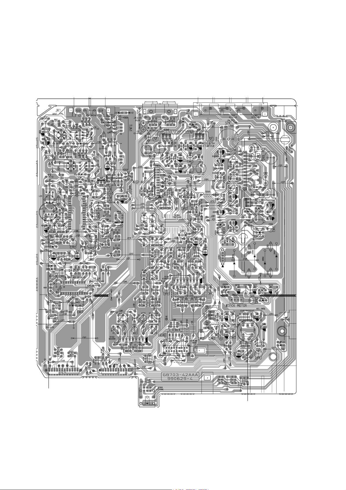
ADJUSTMENT & TEST POINT
Figure 1. Main P.C. Board
L140
(RECORD BIAS
ADJUSTMENT)
L21
(FM IF
ADJUSTMENT)
Page 2
- 9 -
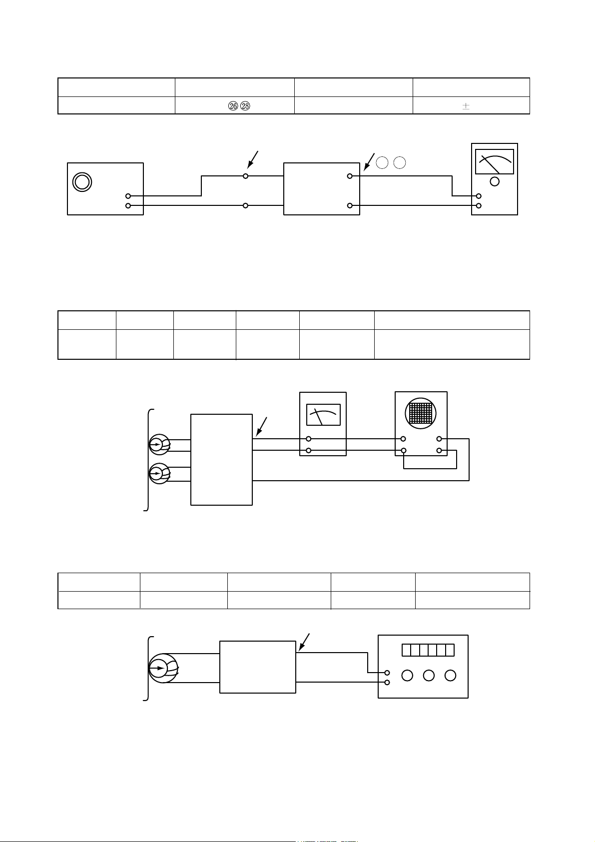
TAPE DECK ADJUSTMENT
1. AZIMUTH ADJUSTMENT
Figure 3. Azimuth Adjustment Connection Diagram
2. RECORD BIAS ADJUSTMENT
Figure 4. Record Bias Adjustment Connection Diagram
TUNER ADJUSTMENT
Figure 2. Tuner(S curve) Adjustment Connection Diagram
CH1 CH2
Speaker
Terminal
Playback Mode
Head
Test Tape
MTT-114
L ch
R ch
GND
Dual-trace
synchroscope
Electronic
Voltmeter
L out
R out
Unit
Unit
26
,
28 PIN
Signal Generator
GND
Electronic
OSCILLOSCOPE
FM Antenna
Terminal
Deck Mode Test Tape Test Point Adjustment Adjust for Remark
Playback MTT-114
Speaker
Head Screw R/L Maximum
Forward:Righthand Side Screw
Terminal Reverse:Lefthand Side Screw
Item Test Point Adjustment Adjust for
DC Voltage IC10
, pin L21 0V 50mV
Deck Mode Test Tape Test Point Adjustment Adjust for
Rec/Pause MTT-5511 Erase Head Wire L140 83kHz±5kHz
Test Tape
MTT-5511
Head
Record/Playback
Head
Record/Playback
and Pause Mode
Unit
Erase Head Wire
GND
Frequency Counter
Page 3

- 10 -
CDP ADJUSTMENTS
When change the pick-up must be confirm as follow
1. TRACKING BALANCE CONFIRMATION
1) Connect the oscilloscope to TEO and REF.(IC501 pin 54 and 71)
2) Access from 1st selection to last section of test disc (YEDS-18)
3) Confirm the normal state of tracking error signal (T.B deviation : less than ±3%)
2. RF WAVEFORM CONFIRMATION
1) Connect the oscilloscope to RF and REF.(IC501 pin 74 and 71)
2) Put a test disc (SONY YEDS-18) into unit and playback the 18th selection of the test disc.
3) Confirm the normal state of RF waveform.
4) Confirm the less than 30nS of Jitter Meter reading.
OV(DC Mode) T.B deviation(%)
= X %
A
B
A=B
A+B
A-B
2
100
3T, 4T 5T,6T 11T
EYE-PATTERN EYE-PATTERN
OK NG
Page 4

- 11 -
¥ Connection : 1. IC501 pin 54.(TEO)
2. IC501 pin 50
¥ Inspection : Check tracking servo
circuit.(RWD)
¥ Connection : 1. IC501 pin 54 .(TEO)
2. IC501 pin 50
¥ Inspection : Check tracking servo
circuit.(RWD)
FOCUS GAIN TRACKING GAIN
¥ Connection : 3. IC502 pin 1 and 2 .
Test disc : YEDS-43
¥ Inspection : Confirm focus servo circuit.
¥ Connection : 3. IC502 pin 26 and 27 .
Test disc: YEDS-43
¥ Inspection : Confirm TRACK servo circuit.
TRACKING ERROR(REW) TRACKING ERROR(FWD)
MAJOR WAVEFORM
ÆV1=0.00V TRIG 1=1.0V
ÆV2=0.00V
DLY>=0.85ms
1V 1V PEAKDET 1ms 1ms
SAVE
ÆT=0.00ms
ÆV1=0.00V TRIG 2=1.0V
ÆV2=0.00V SREF 2 A
DLY>=0.85ms
1V 1V PEAKDET 1ms 1ms
ÆT=0.00ms
ÆV1=0.000V TRIG 1=0.09V
DLY>=4.25ms
0.5V PEAKDET 5ms 5ms
SAVE
ÆT=0.00ms
ÆV1=0.0% TRIG 1=-82%
DLY>=0.170s
>1V PEAKDET 0.2s 50ms
SAVE
ÆT=0.000s
1
2
3
4
1
2
Page 5

- 12 -
TRACKING COIL DRIVE E.F. BALANCE
¥ Connection : 1. IC501 pin 54 . (TEO)
2. IC501 pin 50
¥ Inspection : - Confirm tracking servo circuit.
- Check IC501 (Cold solder joint
or short circuit)
¥ Connection : 1. IC501 pin 54 .
¥ Inspection : Confirm tacking servo balance
deviation rate
READING
¥ Connection : 7. IC501 pin 48 .
8. IC501 pin 40 (FOK)
¥ Inspection : Check IC502 pin 4 to IC501 PIN
48 (Pattern defective)
ÆV1=0.00V TRIG 1=-0.1V
ÆV2=0.00V
DLY>=0.425s
1V 2V PEAKDET 0.5s 50ms
SAVE
ÆT=0.000s
ÆV1=3.96V TRIG 1=1.1V
DLY>=1.70ms
1V PEAKDET 2ms 2ms
SAVE
ÆT=0.00ms
ÆV1=0.00V TRIG 1=0.2V
ÆV2=0.00V
DLY>=0.425s
2V 5V PEAKDET 0.5s 50ms
SAVE
ÆT=0.000s
1
1
2
7
8
Page 6

- 13 -
¥ Connection : 9. IC502 pin 17 and 18
¥ Inspection : - Check IC501 pin 43 to IC502
pin 20 (Pattern defective)
- Check voltage. (IC502 pin 20 )
¥ Connection : 10. IC501 pin 74 .
¥ Inspection : Check objective Lens of Pickup
clear or not
¥ Connection : 11. IC502 pin 1 and 2 .
¥ Inspection : - Is focus search signal output to
IC501 pin 48 ?
¥ Connection : 12. IC501 pin 33 .
¥ Inspection : Check IC503 and surrounding
circuit (Cold solder joint or short
circuit)
TRIG 1=1.1V
ÆV2=0.000V
DLY>=0.085s
0.5V PEAKDET 0.1s 50ms
SAVE
ÆT=0.000s
TRIG 1=24%
DLY>=0.670ms
50mV 0.5ms 0.5ms
ÆV1=0.00V TRIG 1=0.3V
DLY>=0.085s
2V PEAKDET 1s 50ms
SAVESREF 3 A
ÆT=0.00s
>2V
9
11
12
10
 Loading...