

Page 1
Data Sheet
April 19, 2011
4.5 – 5.5Vdc input; 0.8 to 3.63Vdc output; 30A Output Current
6.0 – 14Vdc input; 0.8dc to 5.5Vdc output; 25A Output Current
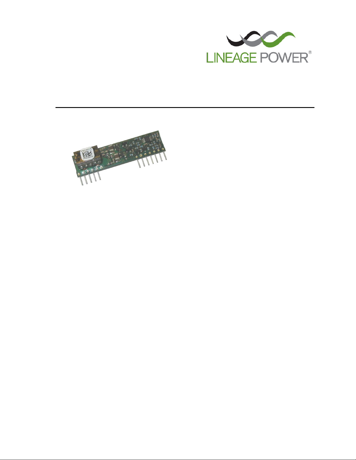
Austin MegaLynxTM: Non-Isolated DC-DC Power Modules:
RoHS Compliant
Applications
Distributed power architectures
Intermediate bus voltage applications
Telecommunications equipment
Servers and storage applications
Networking equipment
Features
Compliant to RoHS EU Directive 2002/95/EC (-
Z versions)
Compliant to ROHS EU Directive 2002/95/EC
with lead solder exemption (non-Z versions)
Delivers up to 30A of output current
High efficiency – 93% 3.3V full load (VIN=12Vdc)
Available in two input voltage ranges
ATH: 4.5 to 5.5Vdc
ATS: 6.0 to 14Vdc
Output voltage programmable from
ATH: 0.8 to 3.63Vdc
ATS: 0.8 to 5.5Vdc
Small size and low profile:
50.8 mm x 12.7 mm x 14.0 mm
2.00 in. x 0.50 in. x 0.55 in.
Monotonic start-up into pre-biased output
Output voltage sequencing (EZ-SEQUENCE
Remote On/Off
Remote Sense
Over current and Over temperature protection
Parallel operation with active current sharing
Wide operating temperature range (-40°C to
85°C)
UL* 60950 Recognized, CSA
60950-00 Certified, and VDE
rd
3
edition) Licensed
ISO** 9001 and ISO 14001 certified
manufacturing facilities
†
C22.2 No.
‡
0805 (EN60950-1
TM
)
Description
The Austin MegaLynx series SIP power modules are non-isolated DC-DC converters in an industry standard
package that can deliver up to 30A of output current with a full load efficiency of 92% at 3.3Vdc output voltage (V
12Vdc). The ATH series of modules operate off an input voltage from 4.5 to 5.5Vdc and provide an output voltage
that is programmable from 0.8 to 3.63Vdc, while the ATS series of modules have an input voltage range from 6 to
14V and provide a programmable output voltage ranging from 0.8 to 5.5Vdc. Both series have a sequencing feature
that enables designers to implement various types of output voltage sequencing when powering multiple modules
on the board. Additional features include remote On/Off, adjustable output voltage, remote sense, over current,
over temperature protection and active current sharing between modules.
* UL is a re gistered trademark of Underwriters Laboratories, Inc.
†
CSA is a reg istered trademark of Canadian Standards Associat ion.
‡
VDE is a t rademark of Verband Deutscher Elektrotechniker e.V.
** ISO is a registered trademark of the International Orga nization of Standards
Document No: DS05-012 ver. 1.06
PDF Name: austin_megalynx_sip.pdf
IN
=
Page 2
Data Sheet
April 19, 2011
4.5 – 5.5Vdc input; 0.8 – 3.63Vdc output; 30A output current
Austin MegaLynxTM: Non-Isolated DC-DC Power Modules:
6.0 – 14Vdc input; 0.8 – 5.5Vdc output; 25A output current
Absolute Maximum Ratings
Stresses in excess of the absolute maximum ratings can cause permanent damage to the device. These are
absolute stress ratings only, functional operation of the device is not implied at these or any other conditions in
excess of those given in the operations sections of the data sheet. Exposure to absolute maximum ratings for
extended periods can adversely affect the device reliability.
Parameter Device Symbol Min Max Unit
Input Voltage
Continuous All V
IN
-0.3 15 Vdc
Sequencing pin voltage All VsEQ -0.3 15 Vdc
Operating Ambient Temperature All T
A
-40 85 °C
(see Thermal Considerations section)
Storage Temperature All T
stg
-55 125 °C
Electrical Specifications
Unless otherwise indicated, specifications apply over all operating input voltage, resistive load, and temperature
conditions.
Parameter Device Symbol Min Typ Max Unit
Operating Input Voltage ATH VIN 4.5 5.0 5.5 Vdc
ATS VIN 6.0 12 14 Vdc
Maximum Input Current ATH I
(VIN= V
IN,min
, VO= V
O,set, IO=IO, max
) ATS I
Inrush Transient All
IN,max
IN,max
2
I
t
Input Reflected Ripple Current, peak-to-peak
(5Hz to 20MHz, 1μH source impedance;
V
=6.0V to 14.0V, IO= I
IN
; See Figure 1)
Omax
All 100 mAp-p
Input Ripple Rejection (120Hz) All 50 dB
27 Adc
26 Adc
2
1
A
s
LINEAGE POWER 2
Page 3

Data Sheet
April 19, 2011
4.5 – 5.5Vdc input; 0.8 – 3.63Vdc output; 30A output current
Austin MegaLynxTM: Non-Isolated DC-DC Power Modules:
6.0 – 14Vdc input; 0.8 – 5.5Vdc output; 25A output current
Electrical Specifications (continued)
Parameter Device Symbol Min Typ Max Unit
Output Voltage Set-point All V
(VIN=V
IN,min
, IO=I
, T
=25°C)
O, max
ref
Output Voltage All V
O, set
O, set
(Over all operating input voltage, resistive
load, and temperature conditions until end
of life)
Adjustment Range
Selected by an external resistor
ATH V
ATS V
0.8 3.63 Vdc
O
O
Output Regulation
Line (VIN=V
Load (IO=I
Temperature (T
IN, min
O, min
to V
to I
ref=TA, min
) All 0.1 % V
IN, max
) All 0.4 % V
O, max
to T
) All 0.5 1 % V
A, max
Output Ripple and Noise on nominal output
(VIN=V
C
OUT
capacitors)
IN, nom
and IO=I
O, min
to I
O, max
= 0.01μF // 0.1μF // 10μF ceramic
Peak-to-Peak (5Hz to 20MHz bandwidth) Vo ≤ 2.5V 50 mV
Peak-to-Peak (5Hz to 20MHz bandwidth) 2.5V < Vo ≤ 3.63V 75 mV
Peak-to-Peak (5Hz to 20MHz bandwidth) Vo > 3.63V 100 mV
External Capacitance
ESR ≥ 1 mΩ All C
ESR ≥ 10 mΩ All C
Output Current (VIN = 5Vdc/12Vdc) ATH025/ATS025 I
Output Current (VIN = 5Vdc) ATH030 I
Output Current Limit Inception (Hiccup
Mode)
All I
Output Short-Circuit Current All I
(VO≤250mV) ( Hiccup Mode )
Efficiency V
VIN=12Vdc, TA=25°C V
IO=25A
, VO
= V
V
O,set
V
V
V
V
Efficiency V
VIN=5Vdc, TA=25°C V
IO=30A
, VO
= V
V
O,set
V
V
V
= 0.8dc η 82.0 %
O,set
= 1.2Vdc η 84.0 %
O,set
= 1.5Vdc η 88.0 %
O,set
= 1.8Vdc η 89.5 %
O,set
= 2.5Vdc η 91.0 %
O,set
= 3.3Vdc η 92.5 %
O,set
= 5.0Vdc η 94.0 %
O,set
= 0.8dc η 84.0 %
O,set
= 1.2Vdc η 88.5 %
O,set
= 1.5Vdc η 90.0 %
O,set
= 1.8Vdc η 91.0 %
O,set
= 2.5Vdc η 93.0 %
O,set
= 3.3Vdc η 95.0 %
O,set
Switching Frequency, Fixed All f
O, max
O, max
o
o
O, lim
O, s/c
sw
-1.5
⎯
–3.0 +3.0 % V
0.8 5.5 Vdc
+1.5 % V
O, set
O, set
O, set
O, set
O, set
pk-pk
pk-pk
pk-pk
0 2,000 µF
0 10,000 µF
0 25 Adc
0 30 Adc
120 % I
20 % I
omax
omax
⎯
300
⎯
kHz
LINEAGE POWER 3
Page 4
Data Sheet
April 19, 2011
4.5 – 5.5Vdc input; 0.8 – 3.63Vdc output; 30A output current
Austin MegaLynxTM: Non-Isolated DC-DC Power Modules:
6.0 – 14Vdc input; 0.8 – 5.5Vdc output; 25A output current
Electrical Specifications (continued)
Parameter Device Symbol Min Typ Max Unit
Dynamic Load Response
(dIO/dt=5A/μs; VIN=VIN,
; VO=3.3V; TA=25°C;)
nom
Load Change from Io= 0% to 50% of IO,max; No
external output capacitors
Peak Deviation ATS V
Settling Time (VO<10% peak deviation)
(dIO/dt=5A/μs; VIN=VIN,
; VO=3.3V; TA=25°C;)
nom
Load Change from IO= 50% to 0%of IO,
external output capacitors
max
: No
ATS t
Peak Deviation ATS V
Settling Time (VO<10% peak deviation)
(dIO/dt=5A/μs; VIN=VIN,
; VO=3.3V; TA=25°C;)
nom
Load Change from Io= 0% to 50% of IO,max; No
external output capacitors
ATS t
Peak Deviation ATH V
Settling Time (VO<10% peak deviation)
(dIO/dt=5A/μs; VIN=VIN,
; VO=3.3V; TA=25°C)
nom
Load Change from IO= 50% to 0%of IO,
external output capacitors
max
: No
ATH t
Peak Deviation ATH V
Settling Time (VO<10% peak deviation)
ATH t
pk
s
pk
s
pk
s
pk
s
⎯
⎯
350
20
⎯
⎯ μs
⎯
⎯
350
20
⎯
⎯ μs
⎯
⎯
320
20
⎯
⎯ μs
⎯
⎯
250
20
⎯
⎯ μs
mV
mV
mV
mV
General Specifications
Parameter Min Typ Max Unit
Calculated MTBF (VIN= V
Telecordia SR 332 Issue 1: Method 1, case 3
Weight
IN, nom
, IO= 0.8I
, TA=40°C)
O, max
3,016,040 Hours
⎯
7.4
⎯
g
LINEAGE POWER 4
Page 5
Data Sheet
,
)
April 19, 2011
4.5 – 5.5Vdc input; 0.8 – 3.63Vdc output; 30A output current
Austin MegaLynxTM: Non-Isolated DC-DC Power Modules:
6.0 – 14Vdc input; 0.8 – 5.5Vdc output; 25A output current
Feature Specifications
Unless otherwise indicated, specifications apply over all operating input voltage, resistive load, and temperature
conditions. See Feature Descriptions for additional information.
Parameter Device Symbol Min Typ Max Unit
On/Off Signal Interface
(VIN=V
Signal referenced to GND)
Logic High (Module OFF)
Input High Current All IIH
Input High Voltage All VIH
Logic Low (Module ON)
Input Low Current All IIL
Input Low Voltage All VIL
Turn-On Delay and Rise Times
(VIN=V
state)
Case 1: On/Off input is enabled and then
input power is applied (delay from instant at
which V
Case 2: Input power is applied for at least one
second and then the On/Off input is enabled (delay
from instant at which Von/Off is enabled until V
10% of V
Output voltage Rise time (time for Vo to rise from
10% of Vo, set to 90% of Vo, set)
Output voltage overshoot 3.0 % V
IO = I
Remote Sense Range All
Over Temperature Protection
(See Thermal Consideration section)
Sequencing Slew rate capability All dVSEQ/dt — 2 V/msec
(V
Sequencing Delay time (Delay from V
to application of voltage on SEQ pin) All TsEQ-delay 10 msec
Tracking Accuracy Power-up (2V/ms) All |VSEQ –Vo,set| 100 200 mV
Power-down (1V/ms) |VSEQ –Vo,set| 200 400 mV
(V
IN, min
Input Undervoltage Lockout
Turn-on Threshold ATH
Turn-off Threshold ATH
Turn-on Threshold ATS
Turn-off Threshold ATS
Forced Load Share Accuracy -P
Number of units in Parallel -P
O, max
IN, min
IN, min
IN, nom
to V
to V
, IO=I
= V
o, set)
; V
IN, min
IN, max
to V
; open collector or equivalent,
IN, max
O, max , VO
until Vo = 10% of Vo
– V
IN, max
; I
IN, max
to I
O, min
; I
- I
O, min
0.5
3.0
⎯
⎯
3.3 mA
V
V
IN, max
⎯ ⎯
-0.3
⎯
200 µA
1.2 V
to within ±1% of steady
All Tdelay ― 3 msec
set
o =
All Tdelay ― 3 msec
All Trise
― 4 msec
O, set
, TA = 25 oC
All T
VSEQ < Vo)
O, max
IN, min
VSEQ < Vo,set)
O, max
ref
⎯ ⎯
⎯
125
4.3 Vdc
3.9 Vdc
5.5 Vdc
5.0 Vdc
⎯
10 % Io
5
0.5 V
⎯
°C
LINEAGE POWER 5
Page 6
Data Sheet
O
/Off
VOLTAGE
OUTPUT
VOLTAGE
April 19, 2011
4.5 – 5.5Vdc input; 0.8 – 3.63Vdc output; 30A output current
Austin MegaLynxTM: Non-Isolated DC-DC Power Modules:
6.0 – 14Vdc input; 0.8 – 5.5Vdc output; 25A output current
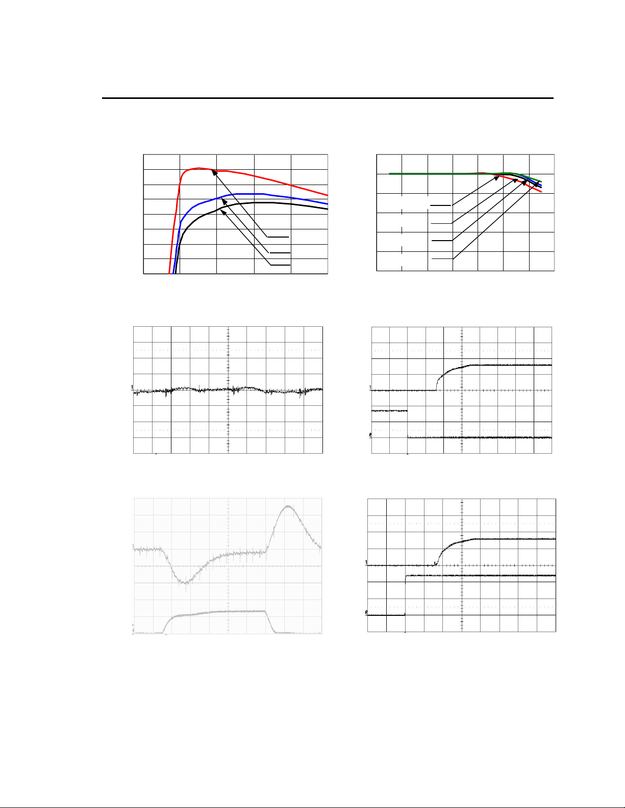
Characteristic Curves
The following figures provide typical characteristics for the ATS025A0X (0.8V, 25A) at 25oC.
92%
89%
86%
83%
80%
77%
74 %
EFFICIENCY, η (%)
71%
68%
0 5 10 15 2 0 2 5
VIN = 6.0V
VIN = 12 .0V
VIN =14.0V
OUTPUT CURRENT, IO (A) AMBIENT TEMPERATURE, TA OC
Figure 1. Converter Efficiency versus Output Current. Figure 4. Derating Output Current versus Local
30
25
20
0.5m/s (100 LFM)
15
1. 0 m/ s ( 2 0 0 LF M )
10
1.5m/ s (3 00 LFM )
5
2.0m/s (400 LFM )
OUTPUT CURRENT, Io (A)
0
20 30 40 50 60 70 80 90
Ambient Temperature and Airflow.
(V) (20mV/div)
O
V
OUTPUT VOLTAGE
TIME, t (1μs/div)
Figure 2. Typical output ripple and noise (V
I
o = Io,max).
(V) (100mV/div)
O
(A) (10A/div) V
O
OUTPUT CURRENT, OUTPUT VOLTAGE
I
TIME, t (5μs /div)
IN = VIN,NOM,
Figure 3. Transient Response to Dynamic Load Change
from 0% to 50% to 0% of full load.
(V) (0.5V/div)
O
(V) (5V/div) V
On/off
n
V
TIME, t (2ms/div)
Figure 5. Typical Start-up Using Remote On/Off (V
V
IN,NOM, Io = Io,max).
(V) (0.5V/div)
O
(V) (5V/div) V
IN
V
INPUT VOLTAGE OUTPUT VOLTAGE
TIME, t (2ms/div)
Figure 6. Typical Start-up Using Input Voltage (VIN =
V
IN,NOM, Io = Io,max).
IN =
LINEAGE POWER 6
Page 7

Data Sheet
OUTPUT
CURRENT
OUTPUT
VOLTAGE
April 19, 2011
4.5 – 5.5Vdc input; 0.8 – 3.63Vdc output; 30A output current
Austin MegaLynxTM: Non-Isolated DC-DC Power Modules:
6.0 – 14Vdc input; 0.8 – 5.5Vdc output; 25A output current
Characteristic Curves
The following figures provide typical characteristics for the ATS025A0X (1.8V, 25A) at 25oC.
96%
93%
90%
87%
84%
81%
78 %
75%
EFFICIENCY, η (%)
72 %
0 5 10 15 2 0 2 5
VIN = 6.0V
VIN = 12 .0V
VIN =14.0V
OUTPUT CURRENT, IO (A) AMBIENT TEMPERATURE, TA OC
Figure 7. Converter Efficiency versus Output Current. Figure 10. Derating Output Current versus Local
30
25
20
0.5m/s (100 LFM)
15
1.0m/s (200 LFM)
10
1.5m/s (300 LFM)
5
2.0m/s (400 LFM )
OUTPUT CURRENT, Io (A)
0
20 30 40 50 60 70 80 90
Ambient Temperature and Airflow ((V
IN = VIN,NOM).
(V) (20mV/div)
O
V
OUTPUT VOLTAGE
TIME, t (1μs/div)
Figure 8. Typical output ripple and noise (V
I
o = Io,max).
(V) (100mV/div)
O
,
(A) (5A/div) V
O
I
TIME, t (5μs /div)
IN = VIN,NOM,
Figure 9. Transient Response to Dynamic Load
Change from 0% to 50% to 0% of full load.
(V) (0.5V/div)
O
(V) (5V/div) V
On/off
V
On/Off VOLTAGE OUTPUT VOLTAGE
TIME, t (2ms/div)
Figure 11. Typical Start-up Using Remote On/Off (V
V
IN,NOM, Io = Io,max).
(V) (0.5V/div)
O
(V) (5V/div) V
IN
V
INPUT VOLTAGE OUTPUT VOLTAGE
TIME, t (2ms/div)
Figure 12. Typical Start-up Using Input Voltage (VIN =
V
IN,NOM, Io = Io,max).
IN =
LINEAGE POWER 7
Page 8

Data Sheet
OU
TPUT
CURRENT
OUTPUT
VOLTAGE
April 19, 2011
4.5 – 5.5Vdc input; 0.8 – 3.63Vdc output; 30A output current
Austin MegaLynxTM: Non-Isolated DC-DC Power Modules:
6.0 – 14Vdc input; 0.8 – 5.5Vdc output; 25A output current
Characteristic Curves
The following figures provide typical characteristics for the ATS025A0X (3.3V, 25A) at 25oC.
99%
96%
93%
90%
87%
84%
81%
EFFICIENCY, η (%)
78 %
75%
0 5 10 15 2 0 2 5
OUTPUT CURRENT, IO (A) AMBIENT TEMPERATURE, TA OC
Figure 13. Converter Efficiency versus Output
Current.
VIN = 6.0V
VIN = 12 .0V
VIN =14.0V
30
25
20
0.5m/s (100 LFM)
15
1.0m/s (200 LFM)
10
1.5m/s (300 LFM)
5
2.0m/s (400 LFM )
OUTPUT CURRENT, Io (A)
0
20 30 40 50 60 70 80 90
Figure 16. Derating Output Current versus Local
Ambient Temperature and Airflow.
(V) (20mV/div)
O
V
OUTPUT VOLTAGE
TIME, t (1μs/div)
Figure 14. Typical output ripple and noise (V
V
IN,NOM, Io = Io,max).
(V) (100mV/div)
O
,
(A) (10A/div) V
O
I
TIME, t (5μs /div)
IN =
Figure 15. Transient Response to Dynamic Load
Change from 0% to 50% to 0% of full load.
(V) (1V/div)
O
(V) (5V/div) V
On/off
V
On/Off VOLTAGE OUTPUT VOLTAGE
TIME, t (2ms/div)
Figure 17. Typical Start-up Using Remote On/Off (V
V
IN,NOM, Io = Io,max).
(V) (1V/div)
O
(V) (5V/div) V
IN
V
INPUT VOLTAGE OUTPUT VOLTAGE
TIME, t (2ms/div)
Figure 18. Typical Start-up Using Input Voltage (VIN =
V
IN,NOM, Io = Io,max).
IN =
LINEAGE POWER 8
Page 9

Data Sheet
April 19, 2011
4.5 – 5.5Vdc input; 0.8 – 3.63Vdc output; 30A output current
Austin MegaLynxTM: Non-Isolated DC-DC Power Modules:
6.0 – 14Vdc input; 0.8 – 5.5Vdc output; 25A output current
Characteristic Curves
The following figures provide typical characteristics for the ATH030A0X (0.8V, 30A) at 25oC.
92%
89%
86%
83%
80%
77%
74 %
71%
EFFICIENCY, η (%)
68%
0 6 12 18 24 30
OUTPUT CURRENT, IO (A) AMBIENT TEMPERATURE, TA OC
Figure 19. Converter Efficiency versus Output
Current.
VIN = 4.5V
VIN = 5.0V
VIN =5.5 V
35
30
25
0.5m/s (100 LFM)
20
1. 0 m/ s ( 2 0 0 LF M )
15
1.5m/ s (3 00 LFM )
10
2.0m/s (400 LFM )
5
OUTPUT CURRENT, Io (A)
20 30 40 50 60 70 80 90
Figure 22. Derating Output Current versus Local
Ambient Temperature and Airflow.
(V) (20mV/div)
O
V
OUTPUT VOLTAGE
TIME, t (1μs/div)
Figure 20. Typical output ripple and noise (V
V
IN,NOM, Io = Io,max).
(V) (100mV/div)
O
(A) (10A/div) V
O
OUTPUT CURRENT, OUTPUT VOLTAGE
I
TIME, t (10μs /div)
IN =
Figure 21. Transient Response to Dynamic Load
Change from 0% to 50% to 0% of full load.
(V) (0.5V/div)
O
(V) (2V/div) V
On/off
V
On/Off VOLTAGE OUTPUT VOLTAGE
TIME, t (2ms/div)
Figure 23. Typical Start-up Using Remote On/Off (V
V
IN,NOM, Io = Io,max).
(V) (0.5V/div)
O
(V) (2V/div) V
IN
V
INPUT VOLTAGE OUTPUT VOLTAGE
TIME, t (2ms/div)
Figure 24. Typical Start-up Using Input Voltage (VIN =
V
IN,NOM, Io = Io,max).
IN =
LINEAGE POWER 9
Page 10

Data Sheet
April 19, 2011
4.5 – 5.5Vdc input; 0.8 – 3.63Vdc output; 30A output current
Austin MegaLynxTM: Non-Isolated DC-DC Power Modules:
6.0 – 14Vdc input; 0.8 – 5.5Vdc output; 25A output current
Characteristic Curves
The following figures provide typical characteristics for the ATH030A0X (1.8V, 30A) at 25oC.
96%
93%
90%
87%
84%
81%
78 %
75%
EFFICIENCY, η (%)
72 %
0 6 12 18 2 4 3 0
OUTPUT CURRENT, IO (A) AMBIENT TEMPERATURE, TA OC
Figure 25. Converter Efficiency versus Output
Current.
VIN = 4.5V
VIN = 5.0V
VIN =5.5V
35
30
25
0.5m/s (100 LFM)
20
1.0m/s (200 LFM)
15
1.5m/s (300 LFM)
10
2.0m/s (400 LFM )
OUTPUT CURRENT, Io (A)
5
20 30 40 50 60 70 80 90
Figure 28. Derating Output Current versus Local
Ambient Temperature and Airflow.
(V) (20mV/div)
O
V
OUTPUT VOLTAGE
TIME, t (1μs/div)
Figure 26. Typical output ripple and noise (V
V
IN,NOM, Io = Io,max).
(V) (100mV/div)
O
(A) (10A/div) V
O
OUTPUT CURRENT, OUTPUT VOLTAGE
I
TIME, t (10μs /div)
IN =
Figure 27. Transient Response to Dynamic Load
Change from 0% to 50% to 0% of full load.
(V) (0.5V/div)
O
(V) (2V/div) V
On/off
V
On/Off VOLTAGE OUTPUT VOLTAGE
TIME, t (2ms/div)
Figure 29. Typical Start-up Using Remote On/Off (V
V
IN,NOM, Io = Io,max).
(V) (0.5V/div)
O
(V) (2V/div) V
IN
INPUT VOLTAGE OUTPUT VOLTAGE
V
TIME, t (2ms/div)
Figure 30. Typical Start-up Using Input Voltage (VIN =
V
IN,NOM, Io = Io,max).
IN =
LINEAGE POWER 10
Page 11

Data Sheet
April 19, 2011
4.5 – 5.5Vdc input; 0.8 – 3.63Vdc output; 30A output current
Austin MegaLynxTM: Non-Isolated DC-DC Power Modules:
6.0 – 14Vdc input; 0.8 – 5.5Vdc output; 25A output current
Characteristic Curves
The following figures provide typical characteristics for the ATH030A0X (3.3V, 30A) at 25oC.
99%
96%
93%
90%
87%
84%
81%
EFFICIENCY, η (%)
78 %
75%
0 6 12 18 2 4 3 0
OUTPUT CURRENT, IO (A) AMBIENT TEMPERATURE, TA OC
Figure 31. Converter Efficiency versus Output
Current.
VIN = 4.5V
VIN = 5.0V
VIN =5.5V
35
30
25
0. 5m/ s (100 LFM )
20
1.0m/s (200 LFM)
15
1.5m/s ( 30 0 LFM )
10
2.0m/s (400 LFM )
OUTPUT CURRENT, Io (A)
5
20 30 40 50 60 70 80 90
Figure 34. Derating Output Current versus Local
Ambient Temperature and Airflow.
(V) (20mV/div)
O
V
OUTPUT VOLTAGE
TIME, t (1μs/div)
Figure 32. Typical output ripple and noise (V
V
IN,NOM, Io = Io,max).
(V) (100mV/div)
O
(A) (10A/div) V
O
OUTPUT CURRENT, OUTPUT VOLTAGE
I
TIME, t (10μs /div)
IN =
Figure 33. Transient Response to Dynamic Load
Change from 0% to 50% to 0% of full load.
(V) (1V/div)
O
(V) (2V/div) V
On/off
V
On/Off VOLTAGE OUTPUT VOLTAGE
TIME, t (2ms/div)
Figure 35. Typical Start-up Using Remote On/Off (V
V
IN,NOM, Io = Io,max).
(V) (1V/div)
O
(V) (2V/div) V
IN
INPUT VOLTAGE OUTPUT VOLTAGE
V
TIME, t (2ms/div)
Figure 36. Typical Start-up Using Input Voltage (VIN =
V
IN,NOM, Io = Io,max).
IN =
LINEAGE POWER 11
Page 12

Data Sheet
F
F
F
F
April 19, 2011
Austin MegaLynxTM: Non-Isolated DC-DC Power Modules:
4.5 – 5.5Vdc input; 0.8 – 3.63Vdc output; 30A output current
6.0 – 14Vdc input; 0.8 – 5.5Vdc output; 25A output current
Test Configurations
V
CIN
150μF
O
V
O
CURRENT PROBE
Min
SCOPE
R
VIN(+)
COM
RESISTIVE
LOAD
contactRdistribution
R
LOAD
TO OSCILLOSCOPE
L
TEST
1μH
CS 220μF
BATTERY
NOTE: Measure input reflected ripple current with a simulated
E.S.R.<0.1Ω
@ 20°C 100kHz
source indu ctance (L
possibl e batter y impedance. M easure cur rent as shown
above.
) of 1μH. Capacitor CS offsets
TEST
Figure 37. Input Reflected Ripple Current Test Setup.
COPPER STRIP
V
(+)
O
GND
NOTE: All voltage measurements to be take n at the module
0.01uF
terminals, as shown above. If sockets are used then
Kelvin connections are required at the module terminals
to avoid measurement errors due to socket contact
resistance.
0.1uF
GROUND PLANE
10uF
Figure 38. Output Ripple and Noise Test Setup.
R
R
contact
distribution
VIN(+)
V
IN
Design Considerations
The Austin MegaLynxTM module should be connected to
a low-impedance source. A highly inductive source can
affect the stability of the module. An input capacitance
must be placed directly adjacent to the input pin of the
module, to minimize input ripple voltage and ensure
module stability.
To minimize input voltage ripple, low-ESR ceramic
capacitors are recommended at the input of the module.
Figure 41 shows the input ripple voltage for various
output voltages at 25A of load current with 2x22 µF or
4x22 µF ceramic capacitors and an input of 12V. Figure
42 shows data for the 5Vin case, with 2x47µF and
4x47µF of ceramic capacitors at the input, and for a load
current of 30A.
180
160
140
120
100
80
60
40
20
0
Input Ripple Voltage (mVp-p)
0.5 1 1.5 2 2.5 3 3.5 4 4.5 5 5.5
Output Voltage (Vdc)
Figure 41. Input ripple voltage for various output
voltages with 2x22 µF or 4x22 µF ceramic capacitors
at the input (25A load). Input voltage is 12V.
60
50
40
2 x 22u
4 x 22u
2 x 47u
4 x 47u
R
R
contact
distribution
NOTE: All volt age meas urements to be taken at th e module
terminals , as shown above. If socket s are us ed then
Kelvin conn ections are requir ed at the modu le termi nals
to avoid measur ement err ors due to soc ket contact
resistance.
COM
COM
R
contactRdistribution
Figure 40. Output Voltage and Efficiency Test Setup.
V
. I
O
Efficiency
=
η
VIN. I
O
IN
x 100 %
30
20
10
0
Input Ripple Voltage (mVp-p)
0.5 1 1.5 2 2.5 3 3.5
Output Voltage (Vdc)
Figure 42. Input ripple voltage in mV, p-p for various
output voltages with 2x47 µF or 4x47 µF ceramic
capacitors at the input (25A load). Input voltage is
5V.
LINEAGE POWER 12
Page 13

Data Sheet
April 19, 2011
Austin MegaLynxTM Non-Isolated dc-dc Power Modules:
4.5 – 5.5Vdc input; 0.8 – 3.63Vdc output; 30A output current
6.0 – 14Vdc input; 0.8 – 5.5Vdc output; 25A output current
Safety Considerations
For safety agency approval the power module must be
installed in compliance with the spacing and separation
requirements of the end-use safety agency standards,
i.e., UL 60950, CSA C22.2 No. 60950-00, EN60950
(VDE 0850) (IEC60950, 3
rd
edition) Licensed.
For the converter output to be considered meeting the
requirements of safety extra-low voltage (SELV), the
input must meet SELV requirements. The power module
has extra-low voltage (ELV) outputs when all inputs are
ELV.
Feature Descriptions
Remote On/Off
The Austin MegaLynx power modules feature a On/Off
pin for remote On/Off operation. If not using the On/Off
pin, connect the pin to ground (the module will be ON).
The On/Off signal (V
configuration for remote On/Off operation of the module
using the On/Off pin is shown in Figure 43.
During a Logic High on the On/Off pin (transistor Q1 is
OFF), the module remains OFF. The external resistor R1
should be chosen to maintain 3.0V minimum on the
On/Off pin to ensure that the module is OFF when
transistor Q1 is in the OFF state. Suitable values for R1
are 4.7K for input voltage of 12V and 3K for 5Vin. During
Logic-Low when Q1 is turned ON, the module is turned
ON.
VIN+
R1
I
ON/OFF
V
ON/OFF
Q1
+
_
ON/OF F
GND
Figure 43. Remote On/Off Implementation using
ON/OFF.
The On/Off pin can also be used to synchronize the
output voltage start-up and shutdown of multiple
modules in parallel. By connecting together the On/Off
pins of multiple modules, the output start-up can be
synchronized (please refer to characterization curves).
When On/Off pins are connected together, all modules
will shut down if any one of the modules gets disabled
) is referenced to ground. Circuit
on/off
MOD UL E
Ther m al SD
1K
10K
PWM Enable
100K
due to undervoltage lockout or over temperature
protection.
Remote Sense
The Austin MegaLynx SIP power modules have a
remote sense feature to minimize the effects of
distribution losses by regulating the voltage at the
remote sense pin (See Figure 44). The voltage between
the Sense pin and the Vo pin must not exceed 0.5V.
The amount of power delivered by the module is defined
as the output voltage multiplied by the output current (Vo
x Io). When using Remote Sense, the output voltage of
the module can increase, which if the same output is
maintained, increases the power output from the module.
Make sure that the maximum output power of the
module remains at or below the maximum rated power.
When the Remote Sense feature is not being used,
connect the Remote Sense pin to output of the module.
R
R
R
Figure 44. Effective Circuit Configuration for Remote
Sense operation.
distribution
distribution
contact
R
contact
VIN(+)
COM
V
Sense
COM
O
R
contactRdistribution
R
LOAD
R
contactRdistribution
Over Current Protection
To provide protection in a fault (output overload)
condition, the unit is equipped with internal
current-limiting circuitry and can endure current limiting
continuously. At the point of current-limit inception, the
unit enters hiccup mode. The unit operates normally
once the output current is brought back into its specified
range. The average output current during hiccup is 20%
I
.
O, max
Over Temperature Protection
To provide protection in a fault condition, the unit is
equipped with a thermal shutdown circuit. The unit will
shutdown if the overtemperature threshold of 130
exceeded at the thermal reference point T
thermal shutdown is not intended as a guarantee that the
unit will survive temperatures beyond its rating. Once
the unit goes into thermal shutdown it will then wait to
cool before attempting to restart.
. The
ref
o
C is
LINEAGE POWER 13
Page 14

Data Sheet
April 19, 2011
4.5 – 5.5Vdc input; 0.8 – 3.63Vdc output; 30A output current
Austin MegaLynxTM: Non-Isolated DC-DC Power Modules:
6.0 – 14Vdc input; 0.8 – 5.5Vdc output; 25A output current
Input Under Voltage Lockout
At input voltages below the input undervoltage lockout
limit, the module operation is disabled. The module will
begin to operate at an input voltage above the
undervoltage lockout turn-on threshold.
Output Voltage Programming
The output voltage of the Austin MegaLynx can be
programmed to any voltage from 0.8dc to 5.0Vdc by
connecting a resistor (shown as Rtrim in Figure 45)
between Trim and GND pins of the module. Without an
external resistor between Trim and GND pins, the output
of the module will be 0.8Vdc. To calculate the value of
the trim resistor, Rtrim for a desired output voltage, use
the following equation:
Rtrim
−
80.0
Vo
1200
= 100
Rtrim is the external resistor in Ω
Vo is the desired output voltage
By using a ±0.5% tolerance trim resistor with a TC of
±100ppm, a set point tolerance of ±1.5% can be
achieved as specified in the electrical specification.
Table 1 provides Rtrim values required for some
common output voltages. The POL Programming Tool,
available at www.lineagepower.com under the Design
Tools section, helps determine the required external trim
resistor needed for a specific output voltage.
V
V
(+)
IN
ON/OFF
GND
(+)
O
TRIM
Figure 45. Circuit configuration to program output
voltage using an external resistor.
Ω
−
LOAD
Rtrim
Table 1
V
(V)
O, set
0.8 Open
1.0 5900
1.2 2900
1.5 1614
1.8 1100
2.5 606
3.3 380
5.0 186
Rtrim (Ω)
Voltage Margining
Output voltage margining can be implemented in the
Austin MegaLynx modules by connecting a resistor,
R
, from the Trim pin to the ground pin for
margin-up
margining-up the output voltage and by connecting a
resistor, R
margin-down
, from the Trim pin to output pin for
margining-down. Figure 46 shows the circuit
configuration for output voltage margining. The POL
Programming Tool, available at www.lineagepower.com
under the Design Tools section, also calculates the
values of R
margin-up
and R
margin-down
for a specific output
voltage and % margin. Please consult your local
Lineage Power technical representative for additional
details.
Voltage Sequencing
The Austin MegaLynx series of modules include a
sequencing feature that enables users to implement
various types of output voltage sequencing in their
applications. This is accomplished via an additional
sequencing pin. When not using the sequencing feature,
either leave the SEQ pin unconnected or tied to V
Vo
Rmargin-down
Austin Lynx or
Lynx II Series
Trim
Q2
Rmargin-up
IN.
Rtrim
Q1
GND
Figure 46. Circuit Configuration for margining
Output voltage.
LINEAGE POWER 14
Page 15

Data Sheet
April 19, 2011
Austin MegaLynxTM Non-Isolated dc-dc Power Modules:
4.5 – 5.5Vdc input; 0.8 – 3.63Vdc output; 30A output current
6.0 – 14Vdc input; 0.8 – 5.5Vdc output; 25A output current
For proper voltage sequencing, first, input voltage is
applied to the module. The On/Off pin of the module is
left unconnected or tied to GND for negative logic
modules so that the module is ON by default. After
applying input voltage to the module, a delay of 10msec
minimum is required before applying voltage on the SEQ
pin. During this delay time, the SEQ pin should be kept
at a voltage of 50mV (± 20 mV). After the 10msec delay,
the voltage applied to the SEQ pin is allowed to vary and
the output voltage of the module will track this voltage on
a one-to-one volt basis until the output reaches the setpoint voltage. To initiate simultaneous shutdown of the
modules, the sequence pin voltage is lowered in a
controlled manner. The output voltages of the modules
track the sequence pin voltage when it falls below their
set-point voltages. A valid input voltage must be
maintained until the tracking and output voltages reach
zero to ensure a controlled shutdown of the modules.
For a more detailed description of sequencing, please
refer to Application Note AN04-008 titled “Guidelines
for Sequencing of Multiple Modules”.
When using the EZ-SEQUENCE
start-up of the module, pre-bias immunity feature during
start-up is disabled. The pre-bias immunity feature of
the module relies on the module being in the diode-mode
during start-up. When using the EZ-SEQUENCE
feature, modules goes through an internal set-up time of
10msec, and will be in synchronous rectification mode
when voltage at the SEQ pin is applied. This will result
in sinking current in the module if pre-bias voltage is
present at the output of the module. When pre-bias
immunity during start-up is required, the EZSEQUENCE
TM
feature must be disabled.
TM
feature to control
TM
Active Load Sharing (-P Option)
For additional power requirements, the Austin MegaLynx
series power module is also available with a parallel
option. Up to five modules can be configured, in parallel,
with active load sharing. Good layout techniques should
be observed when using multiple units in parallel. To
implement forced load sharing, the following connections
should be made:
• The share pins of all units in parallel must be
connected together. The path of these connections
should be as direct as possible.
• All remote-sense pins should be connected to the
power bus at the same point, i.e., connect all the
SENSE
(+) pins to the (+) side of the bus. Close
proximity and directness are necessary for good
noise immunity
Some special considerations apply for design of
converters in parallel operation:
• When sizing the number of modules required for
parallel operation, take note of the fact that current
sharing has some tolerance. In addition, under
transient condtions such as a dynamic load change
and during startup, all converter output currents will
LINEAGE POWER 15
not be equal. To allow for such variation and avoid
the likelihood of a converter shutting off due to a
current overload, the total capacity of the paralleled
system should be no more than 75% of the sum of
the individual converters. As an example, for a
system of four ATS030A0X3-SR converters the
parallel, the total current drawn should be less that
75% of (4 x 30A) , i.e. less than 90A.
• All modules should be turned on and off together.
This is so that all modules come up at the same time
avoiding the problem of one converter sourcing
current into the other leading to an overcurrent trip
condition. To ensure that all modules come up
simultaneously, the on/off pins of all paralleled
converters should be tied together and the
converters enabled and disabled using the on/off
pin.
• The share bus is not designed for redundant
operation and the system will be non-functional
upon failure of one of the unit when multiple units
are in parallel. In particular, if one of the converters
shuts down during operation, the other converters
may also shut down due to their outputs hitting
current limit. In such a situation, unless a
coordinated restart is ensured, the system may
never properly restart since different converters will
try to restart at different times causing an overload
condition and subsequent shutdown. This situation
can be avoided by having an external output voltage
monitor circuit that detects a shutdown condition
and forces all converters to shut down and restart
together.
Page 16

Data Sheet
W
April 19, 2011
4.5 – 5.5Vdc input; 0.8 – 3.63Vdc output; 30A output current
Austin MegaLynxTM: Non-Isolated DC-DC Power Modules:
6.0 – 14Vdc input; 0.8 – 5.5Vdc output; 25A output current
Thermal Considerations
Power modules operate in a variety of thermal
environments; however, sufficient cooling should always
be provided to help ensure reliable operation.
Considerations include ambient temperature, airflow,
module power dissipation, and the need for increased
reliability. A reduction in the operating temperature of the
module will result in an increase in reliability. The
thermal data presented here is based on physical
measurements taken in a wind tunnel. The test set-up is
shown in Figure 47. Note that the airflow is parallel to
the long axis of the module as shown in Figure 48. The
derating data applies to airflow in either direction of the
module’s long axis.
ind Tunnel
PWBs
25.4_
(1.0)
Power Module
76.2_
(3.0)
x
Back View
Figure 48. T
The thermal reference point, T
specifications is shown in Figure 48. For reliable
operation this temperature should not exceed 125
The output power of the module should not exceed the
rated power of the module (Vo,set x Io,max).
Please refer to the Application Note “Thermal
Characterization Process For Open-Frame BoardMounted Power Modules” for a detailed discussion of
thermal aspects including maximum device
temperatures.
Temperature measurement location.
ref
used in the
ref
o
C.
Probe Location
12.7_
(0.50)
Air
for measuring
airflow and
ambient
temperature
flow
Figure 47. Thermal Test Set-up.
LINEAGE POWER 16
Page 17

Data Sheet
April 19, 2011
Austin MegaLynxTM Non-Isolated dc-dc Power Modules:
4.5 – 5.5Vdc input; 0.8 – 3.63Vdc output; 30A output current
6.0 – 14Vdc input; 0.8 – 5.5Vdc output; 25A output current
Mechanical Outline of Module
Dimensions are in millimeters and (inches).
Tolerances: x.x mm ± 0.5 mm (x.xx in. ± 0.02 in.) [unless otherwise indicated]
x.xx mm ± 0.25 mm (x.xxx in ± 0.010 in)
BACK SIDE VIEW
Pin out
Pin Function
1 Vo
2 Vo
3 Sense+
4 Vo
5 GND
6 GND*
7 Share**
8 GND
9 VIN
10 VIN
11 SEQ
12 Trim
13 On/Off
Pin 6 is added in
ATH030A0X3 version
** Pin 7 is paralleling
option
LINEAGE POWER 17
Page 18

Data Sheet
April 19, 2011
4.5 – 5.5Vdc input; 0.8 – 3.63Vdc output; 30A output current
Austin MegaLynxTM: Non-Isolated DC-DC Power Modules:
6.0 – 14Vdc input; 0.8 – 5.5Vdc output; 25A output current
Recommended Pad Layout
Dimensions are in millimeters and (inches).
Tolerances: x.x mm ± 0.5 mm (x.xx in. ± 0.02 in.) [unless otherwise indicated]
x.xx mm ± 0.25 mm (x.xxx in ± 0.010 in)
LINEAGE POWER 18
Page 19

Data Sheet
April 19, 2011
Austin MegaLynxTM Non-Isolated dc-dc Power Modules:
4.5 – 5.5Vdc input; 0.8 – 3.63Vdc output; 30A output current
6.0 – 14Vdc input; 0.8 – 5.5Vdc output; 25A output current
Through-Hole Lead-Free Soldering
Information
The RoHS-compliant through-hole products use the
SAC (Sn/Ag/Cu) Pb-free solder and RoHS-compliant
components. They are designed to be processed
through single or dual wave soldering machines. The
pins have an RoHS-compliant finish that is compatible
with both Pb and Pb-free wave soldering processes.
A maximum preheat rate of 3°C/s is suggested. The
wave preheat process should be such that the
temperature of the power module board is kept below
210°C. For Pb solder, the recommended pot
temperature is 260°C, while the Pb-free solder pot is
270°C max. Not all RoHS-compliant through-hole
products can be processed with paste-through-hole
Pb or Pb-free reflow process. If additional information
is needed, please consult with your Lineage Power
technical representative for more details.
LINEAGE POWER 19
Page 20

Data Sheet
a
©
April 19, 2011
4.5 – 5.5Vdc input; 0.8 – 3.63Vdc output; 30A output current
Austin MegaLynxTM: Non-Isolated DC-DC Power Modules:
6.0 – 14Vdc input; 0.8 – 5.5Vdc output; 25A output current
Ordering Information
Please contact your Lineage Power Sales Representative for pricing, availability and optional features.
Table 2. Device Codes
Input Voltage Output Voltage
Output
Current
4.5 – 5.5Vdc 0.8 – 3.63Vdc 25A Negative SIP ATH025A0X3 108991980
4.5 – 5.5Vdc 0.8 – 3.63Vdc 25A Negative SIP ATH025A0X3Z CC109104774
4.5 – 5.5Vdc 0.8 – 3.63Vdc 30A Negative SIP ATH030A0X3 108992005
4.5 – 5.5Vdc 0.8 – 3.63Vdc 30A Negative SIP ATH030A0X3Z CC109104782
4.5 – 5.5Vdc 0.8 – 3.63Vdc 30A Negative SIP ATH030A0X3-P 108993358
4.5 – 5.5Vdc 0.8 – 3.63Vdc 30A Negative SIP ATH030A0X3-PZ CC109104790
6.0 – 14Vdc 0.8– 5.5Vdc 25A Negative SIP ATS025A0X3 108991997
6.0 – 14Vdc 0.8– 5.5Vdc 25A Negative SIP ATS025A0X3Z CC109104808
6.0 – 14Vdc 0.8– 5.5Vdc 25A Negative SIP ATS025A0X53 108997210
6.0 – 14Vdc 0.8– 5.5Vdc 25A Negative SIP ATS025A0X3-P 108993341
6.0 – 14Vdc 0.8– 5.5Vdc 25A Negative SIP ATS025A0X3-PZ CC109104816
6.0 – 14Vdc 0.8– 5.5Vdc 25A Negative SIP ATS025A0X53-PZ CC109107752
6.0 – 14Vdc 0.8– 5.5Vdc 25A Negative SIP ATS025A0X3-34Z* CC109147897
* Special part, consult factory before ordering
Table 3. Device Options
Option Device Code Suffix
Long pins 5.08mm ± 0.25m (0.2 in. ± 0.010 in.) -5
Paralleling with active current sharing -P
RoHS Compliant -Z
On/Off
Logic
Connector
Type
Product codes Comcodes
Asia-Pacific Headquarters
Tel: +86.021.54279977*808
World Wide Headquarters
Lineage Power Corporation
601 Shiloh Road, Plano, TX 75074, USA
+1-888-LINEAGE(546-3243)
(Outside U.S.A.: +1-972-244-WATT(9288))
www.lineagepower.com
e-mail: techsupport1@lineagepower.com
Europe, Middle-East and Africa Headquarters
Tel: +49.89.878067-280
India Headquarters
Tel: +91.80.28411633
Lineage Power reserves the right to make changes to the product(s) or information contained herein without notice. No liability is assumed as a result of their use or
pplication. No rights under any patent accompany the sale of any such product(s) or information.
Lineage Power DC-DC products are protected under various patents. Information on these patents is available at www.lineagepower.com/patents.
2011 Lineage Power Corporation, (Plano, Texas) All International Rights Reserved.
LINEAGE POWER 20
Document No: DS05-012 ver. 1.06
PDF Name: austin_megalynx_sip.pdf
 Loading...