

Page 1
SERVICE MANUAL
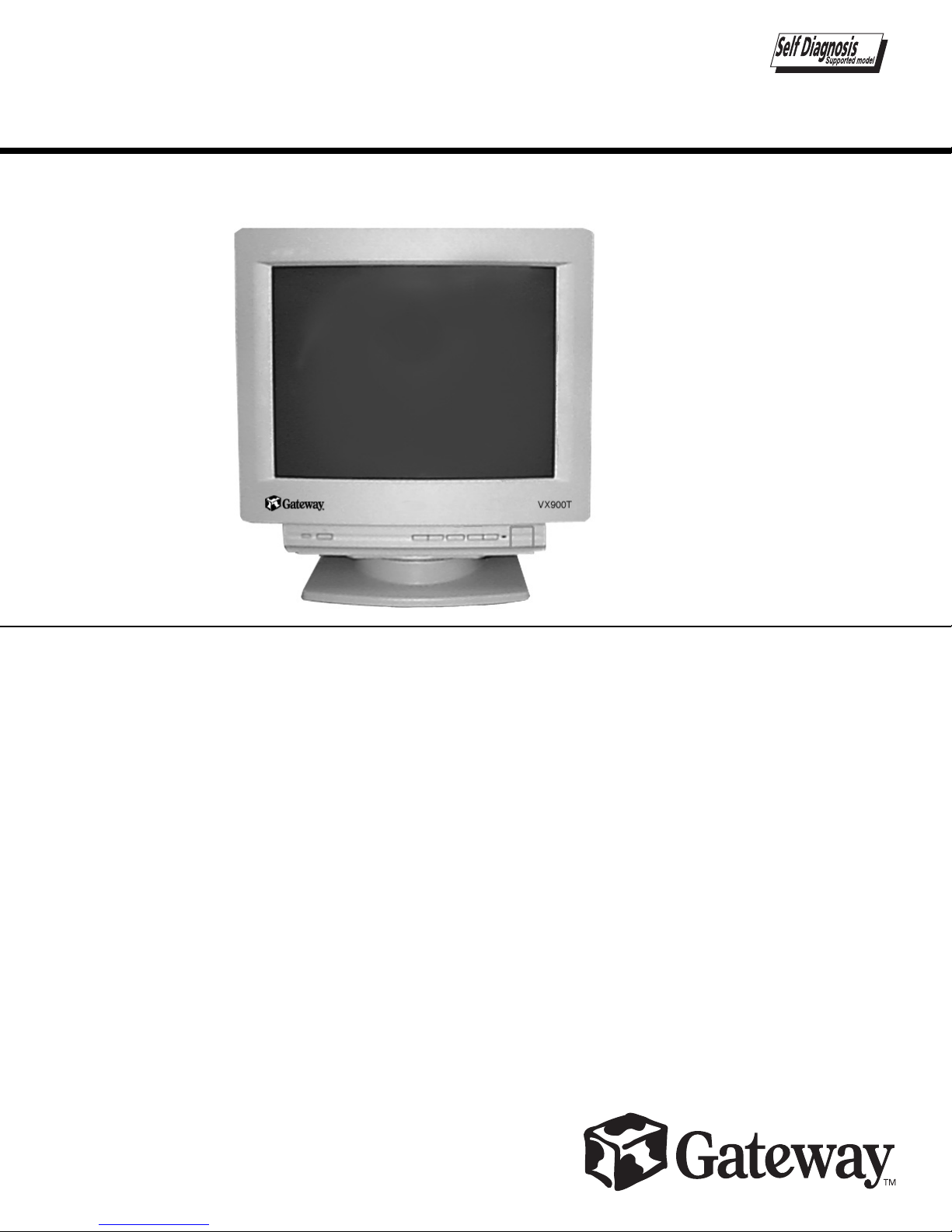
VX900T
VX900T
VX900T
US Model
Canadian Model
Chassis No. SCC-L20F-A
Picture tube
Video image area
Resolution
Standard image area
Input signal
Video
Sync
SPECIFICATIONS
0.25-0.27 mm aperture grill pitch
19 inches measured diagonally
90-degree deflection
(18" maximum viewing image)
Approx. 365 X 274 mm (w/h)
3/8
7/8
x 10
x 10
7/8
inches)
1/2
inches)
(14
Horizontal: Max. 1600 dots
Vertical: Max. 1200 lines
Approx. 352 x 264 mm (w/h)
(13
Analog RGB (75 ohms typical)
0.7 Vp-p, Positive
External HD/VD, Composite
Polarity Free TTL
Video Composite (Sync on Green)
0.3 Vp-p, Negative
D98
Power Consumption
Maximum
Nominal
Deflection frequency
AC input voltage / current
Dimensions
Mass
Design and specifications are subject to change without notice.
130 W
100 W
Horizontal: 30 to 96 KHz
Vertical: 48 to120 Hz
100 to 120 V, 50/60 Hz, 1.7A
220 to 240V, 50/60Hz, 1.2A
444 x 467 x 455 (w/h/d)
(17
Approx. 26 kg (57 lb 5 oz)
CHASSIS
1/2
1/2
x 18
x 18 inches)
COLOR MONITOR
— 1 —
Page 2
VX900T
(
µ
)
POWER SAVING FUNCTION
This monitor has three Power Saving modes.
By sensing the absence of a video signal from the
computer, it reduces power consumption as follows:
Power Required Recovery
State Consumption Time Power Indicator
1
Normal Operation
2 Standby (1st mode)
3 Suspend (2nd mode)
4 Active-off (3rd mode)
< 125W Green on
< 15W approx. 3 sec. Green and orange alternate
< 15W approx. 3 sec. Green and orange alternate
< 8W approx. 10 sec. Orange
5 Power-off 0.2W Off
6 Failure modes See below
SELF DIAGNOSIS FUNCTION
When a failure occurs, the STANDBY/TIMER lamp will flash a set number of times to indicate
the possible cause of the problem. If there is more than one error, the lamp will
identify the first of the problem areas.
Status Area of Failure LED Indication
1 Failure 1 HV or B+ Orange (0.5 second)/Off (0.5 second)
2 Failure 2 H Stop, V Stop, Thermal Orange (1.5 second)/Off (0.5 second)
3 Failure 3 ABL Orange (0.5 second)/Off (1.5 second)
4 Aging/Self Test Orange (0.5 second)/Off (0.5 second)/
NOTE:
If no video signal is input to the monitor, the
"NO INPUT SIGNAL" message appears. After
about 30 seconds, the Power Saving function
automatically puts the monitor into active-off
mode and the indicator lights up orange. Once
the monitor detects horizontal and vertical sync
signals, the monitor automatically resumes
normal operation mode.
Green (0.5 second)/Off(0.5 second)
TIMING SPECIFICATION
MODE 123
Resolution (H x V) 720 X 400 1280 X 1024 1600 X 1200
Dot Clock (MHz) 28.321 135.000 202.500
HORIZONTAL
Hor. Freq. (kHz) 31.468 79.976 93.750
Ext (H/V)/Polarity Yes -/+ Yes +/+ Yes +/+
Ext (CS)/Polarity No No No
H-Total 31.779 12.504 10.667
H-Blanking 6.356 3.022 2.765
H-Front Porch 0.636 0.119 0.316
H-Sync. 3.178 1.067 0.948
H-Back Porch 2.542 1.837 1.501
H-Active 25.423 9.481 7.901
sec
VERTICAL
Ver. Freq. (Hz) 70.084 75.025 75.000
V-Total 449 1066 1250
V-Blanking 4 9 42 5 0
V-Front Porch 1 3 1 1
V-Sync. 2 3 3
V-Back Porch 3 4 3 8 4 6
V-Active 400 1024 1200
(lines)
SYNC.
Int (G) No No No
Int/Non Int Non Int Non Int Non Int
— 2 —
Page 3
SAFETY CHECK-OUT
VX900T
After correcting the original service problem, perform
the following safety checks before releasing the set to the
customer:
1.Check the area of your repair for unsoldered or
poorly-soldered connections. Check the entire board
surface for solder splashes and bridges.
2.Check the interboard wiring to ensure that no wires
are “pinched” or contact high-wattage resistors.
3.Check that all control knobs, shields, covers, ground
straps, and mounting hardware have been replaced.
Be absolutely certain that you have replaced all the
insulators.
4.Look for unauthorized replacement parts,
particularly transistors, that were installed during
a previous repair. Point them out to the customer
and recommend their replacement.
5.Look for parts which, though functioning, show
obvious signs of deterioration. Point them out to
the customer and recommend their replacement.
6.Check the line cords for cracks and abrasion.
Recommend the replacement of any such line cord
to the customer.
7.Check the B+ and HV to see if they are specified
values. Make sure your instruments are accurate;
be suspicious of your HV meter if sets always have
low HV.
8.Check the antenna terminals, metal trim,
“metallized" knobs, screws, and all other exposed
metal parts for AC Leakage. Check leakage as
described below.
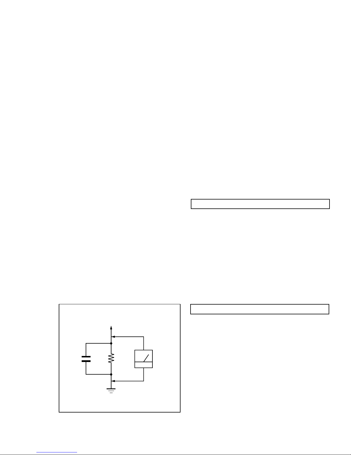
LEAKAGE TEST
The AC leakage from any exposed metal part to earth ground
and from all exposed metal parts to any exposed metal part having
a return to chassis, must not exceed 0.5 mA (500 microampere).
Leakage current can be measured by any one of three methods.
1.A commercial leakage tester, such as the Simpson 229 or
RCA WT-540A. Follow the manufacturers' instructions to
use these instructions.
2.A battery-operated AC milliammeter. The Data Precision
245 digital multimeter is suitable for this job.
3.Measuring the voltage drop across a resistor by means of
a VOM or battery-operated AC voltmeter. The "limit"
indication is 0.75 V, so analog meters must have an accurate
low voltage scale. The Simpson's 250 and Sanwa
SH-63Trd are examples of passive VOMs that are suitable.
Nearly all battery operated digital multimeters that have a
2V AC range are suitable. (See Fig. A)
WARNING!!WARNING!!
WARNING!!
WARNING!!WARNING!!
NEVER TURN ON THE POWER IN A CONDITION IN WHICH THE
DEGAUSS COIL HAS BEEN REMOVED.
SAFETY-RELATED COMPONENT WARNING!!
COMPONENTS IDENTIFIED BY SHADING AND MARK ¡ ON
THE SCHEMATIC DIAGRAMS, EXPLODED VIEWS AND IN THE
PARTS LIST ARE CRITICAL FOR SAFE OPERATION. REPLACE
THESE COMPONENTS WITH SONY PARTS WHOSE PART
NUMBERS APPEAR AS SHOWN IN THIS MANUAL OR IN
SUPPLEMENTS PUBLISHED BY SONY. CIRCUIT ADJUSTMENTS
THAT ARE CRITICAL FOR SAFE OPERATION ARE IDENTIFIED
IN THIS MANUAL. FOLLOW THESE PROCEDURES WHENEVER
CRITICAL COMPONENTS ARE REPLACED OR IMPROPER
OPERATION IS SUSPECTED.
To Exposed Metal
Parts on Set
0.15 µF
1.5 k
W
Earth Ground
AC
Voltmeter
(0.75 V)
AVERTISSEMENT!!
NE JAMAIS METTRE SOUS TENSION QUAND LA BOBINE DE
DEMAGNETISATION EST ENLEVEE.
ATTENTION AUX COMPOSANTS RELATIFS A LA
SECURITE!!
LES COMPOSANTS IDENTIFIES PAR UNE TRAME ET PAR UNE
MARQUE ¡ SUR LES SCHEMAS DE PRINCIPE, LES VUES
EXPLOSEES ET LES LISTES DE PIECES SONT D'UNE
IMPORTANCE CRITIQUE POUR LA SECURITE DU
FONCTIONNEMENT. NE LES REMPLACER QUE PAR DES
COMPOSANTS SONY DONT LE NUMERO DE PIECE EST
INDIQUE DANS LE PRESENT MANUEL OU DANS DES SUPPLEMENTS PUBLIES PAR SONY. LES REGLAGES DE CIRCUIT
DONT L'IMPORTANCE EST CRITIQUE POUR LA
SECURITE DU FONCTIONNEMENT SONT IDENTIFIES DANS
LE PRESENT MANUEL. SUIVRE CES PROCEDURES LORS DE
CHAQUE REMPLACEMENT DE COMPOSANTS CRITIQUES, OU
LORSQU'UN MAUVAIS FONTIONNEMENT SUSPECTE
— 3 —
.
Page 4

VX900T
TABLE OF CONTENTS
Section Title Page
1. GENERAL ................................................................................... 5
2. DISASSEMBLY
2-1. Cabinet Removal ............................................................11
2-2. Service Position .............................................................. 11
2-3. D, A, H and N Board Removal......................................11
2-4. Picture Tube Removal ................................................... 12
3. SAFETY RELA TED ADJUSTMENT................................. 13
4. ADJUSTMENTS ........................................................................14
5. DIAGRAMS
5-1. Block Diagram ................................................................19
5-2. Circuit Boards Location ................................................. 22
5-3. Schematic Diagrams and Printed Wiring Boards ...... 22
1. D Board - Schematic Diagram .................................23
2. A Board - Schematic Diagram ................................. 27
3. N Board - Schematic Diagram .................................. 31
4. H Board - Schematic Diagram .................................. 35
5-4. Semiconductors ............................................................. 37
6. EXPLODED VIEWS
6-1. Chassis .................. ......................................................... 39
6-2. Packing Materials .......................................................... 40
7. ELECTRICAL PARTS LIST ................................................ 41
— 4 —
Page 5
— 5 —
VX900T
SECTION 1
GENERAL
The instructions given here are partial abstracts from the Operating Instruction
Manual. The page numbers shown reflect those of the Operating Instruction Manual.
3
Getting Started
US
Table of Contents
Precautions. . . . . . . . . . . . . . . . . . . . . . . . . . . . . . . . . . 3
Setup. . . . . . . . . . . . . . . . . . . . . . . . . . . . . . . . . . . . . . . 4
Parts and Controls . . . . . . . . . . . . . . . . . . . . . . . . . . . . 4
The OSD (On-screen Display) System. . . . . . . . . . . . . 6
Resetting the adjustments . . . . . . . . . . . . . . . . . . . . . 10
Specifications . . . . . . . . . . . . . . . . . . . . . . . . . . . . . . . 11
Monitor Information. . . . . . . . . . . . . . . . . . . . . . . . . . . 11
Power Saving Function and LED Indicators. . . . . . . . 11
If thin lines appear on your screen (damper wires). . . 11
Warning Messages. . . . . . . . . . . . . . . . . . . . . . . . . . . 12
Troubleshooting . . . . . . . . . . . . . . . . . . . . . . . . . . . . . 12
Precautions
Do not install the monitor in the following places:
• on surfaces (rugs, blankets, etc.) or near materials (curtains,
draperies) that may block the ventilation holes
• near heat sources such as radiators or air ducts, or in a place
subject to direct sunlight
• in a place subject to severe temperature changes
• in a place subject to mechanical vibration or shock
• on an unstable surf ac e
• near equ ipme nt which generates magnetism, such as a
transformer or high voltage power lines
• near or on an electrically charged metal surface
• Clean the screen with a soft cloth. If you use a glass cleaning
liquid, do not use any type of cleaner containing an anti-static
solution or similar additive as this may scratch the screen’s
coating.
• Do not rub, touch, or tap the surface of the screen with sharp or
abrasive items such as a ball point pen or screwdriver. This type
of contact may result in a scratched picture tube.
• Clean the cabinet, panel and controls with a soft cloth lightly
moistened with a mild detergent solut ion. Do not use any type of
abrasive pad, scouring powder or solvent, such as alcohol or
benzene.
When you transport this monitor for repair or shipment, use the
original carton and packing materials.
• Use the supplied power cord. If you use a different power cord,
be sure that it is compatible with your local power supply.
For the customers in the US
If you do not use the appropriate cord, this monitor will not
conform to mandatory FCC Standards.
• Before disconnecting the power cord, wait at least 30 seconds
after turning off the power to allow the static electricity on the
screen’s surface to discharge.
• After the power is turned on, the screen is demagnetized
(degaussed) for about 3 seconds. This generates a strong
magnetic field around the screen, which may affect data stored on
magnetic tap es and disks placed near the monitor. Be sure to keep
magnetic recording equipment, tapes and disks away from the
monitor.
Installation
Maintenance
Transportation
Warning on power Connection
The equipment should be installed near an easily accessible
outlet.
Example of plug types
for 100 to 120 V AC for 200 to 240 V AC
4
Getting Started
Setup
Connect the monitor to your computer system.
This monitor will sync to platforms running at horizontal frequencies between 30 and 96 kHz.
Step 1
Make sure the compuer system is switched off and attach
the video signal cable to the video output of the computer.
Step 2
Make sure the compuer is switched off and attach the
power cord the monitor. Then, attach the other end of the
power cord to a power outlet.
Step 3
Switch on the monitor and computer.
Step 4
Adjust the user controls according to your personal
preference.
Installation is complete.
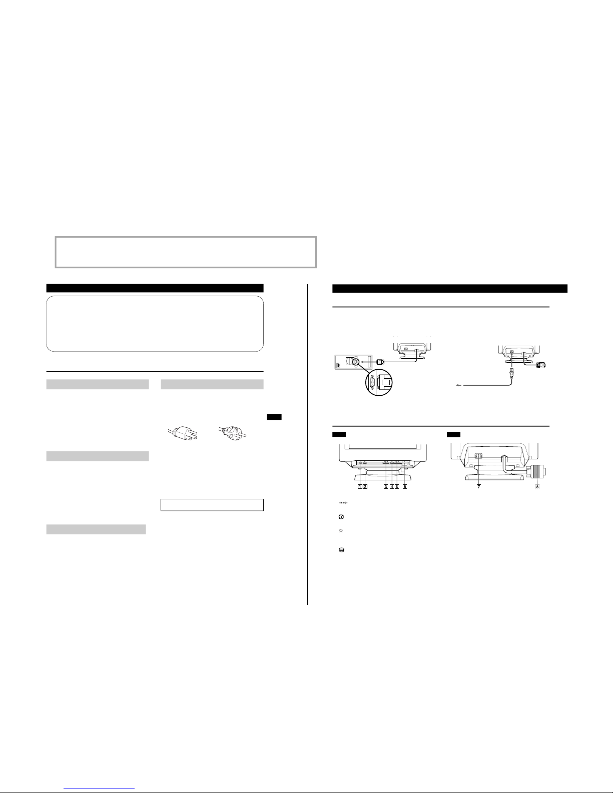
Parts and Controls
1 (RESET) button (pages 6, 10)
Resets the adjustments to the factory settings.
2 Auto Sizing and Centering button (page 5)
Automatically adjusts the picture size and position.
3 (BRIGHTNESS) (v/V) buttons (page 5)
Adjust the picture brightness.
Operate as the (v/V) buttons when adjusting other items.
4 (MENU) button (page 6)
Displays the MENU OSD.
5 6 (CONTRAST) (B/b) buttons (page 5)
Adjust the contrast.
Operate as the (B/b) buttons when adjusting other items.
6 1 (POWER) switch and indicator
Turns the monitor on and off.
The indicator lights up green when the monitor is on, and lights
up green and orange when the monitor is in Power Saving
mode.
7 AC IN connector
Provides AC power to the monitor.
8 Video input connector (HD15) (page 5)
Inputs RGB video signals and SYNC signals.
Computer
to the video output
to a power outlet
Power cord
Front
Rear
Page 6
— 6 —
VX900T
5
Getting Started
Customizing Your Monitor
US
This monitor can be adjusted within the angles shown below. To
turn the monitor vertically or horiz onta lly, hold it at the bottom with
both hands.
1
Press the (BRIGHTNESS)
v/V
or 6 (CONTRAST)
B/b
buttons.
The BRIGHTNESS/CONTRAST OSD appeears.
2
To adjust the brightness.
Press the (BRIGHTNESS) v/V buttons.
To adjust the contrast.
Press the 6 (CONTRAST) B/b buttons.
You can easily adjust the picture to fill the screen by pressing the
Auto Sizing and Centering button.
Press the Auto Sizing and Centering button.
The picture automatically fills the screen.
Note
This function is intended for use with a computer running Windows or
similar graphic user interface software that provides a full-screen picture. It
may not work properly if the background color is dark or if the input picture
does not fill the screen to the edges (such as an MS-DOS prompt).
Use of the Tilt/Swivel
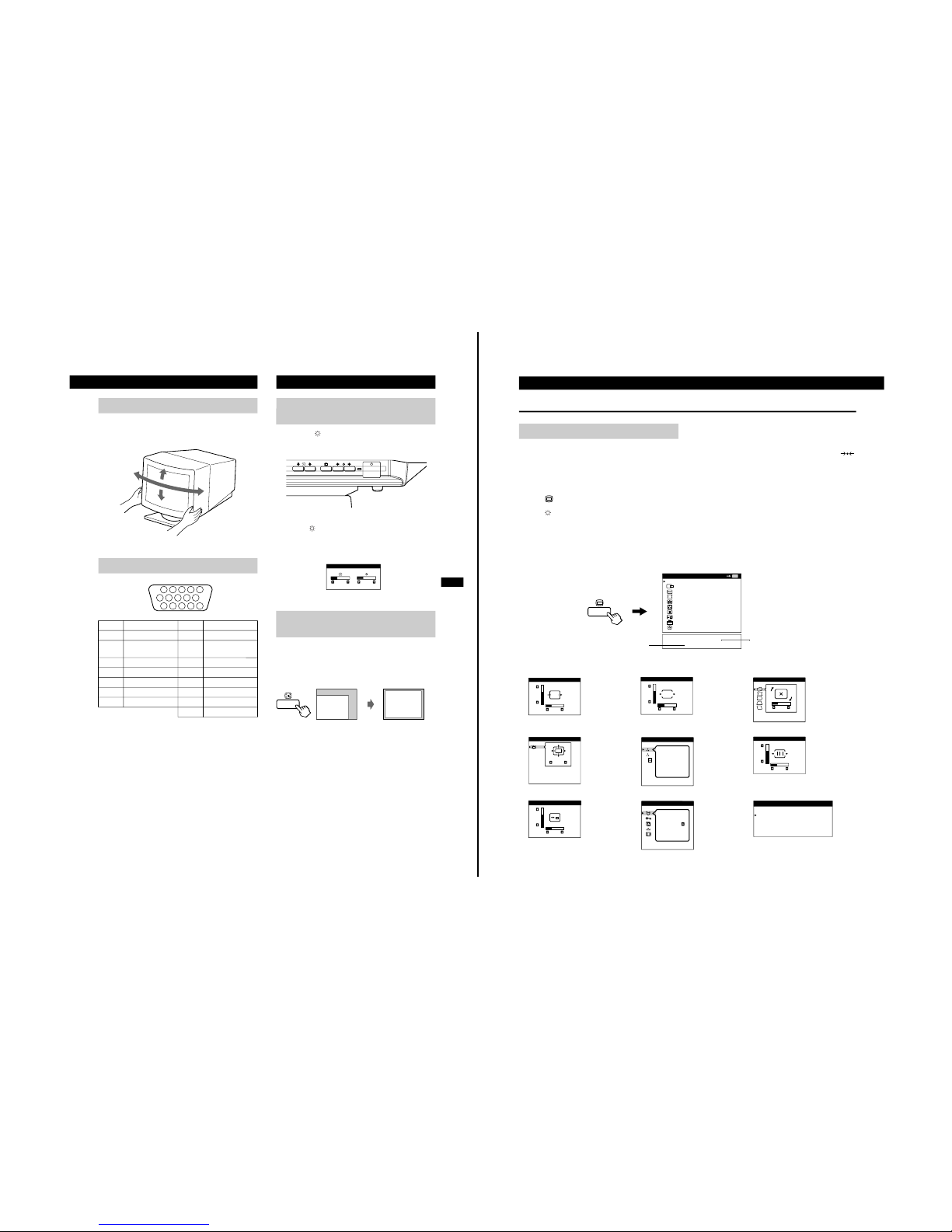
Video Connector
Pin No. Signal Pin No. Signal
1 Red 8 Blue Ground
2 Green (Composite
Sync on Green)
9 Not used (no pin)
3Blue 10Ground
4Ground 11Ground
5CPU Snense 12 SDA (serial data)
6 Red Ground 13 Horizontal Sync
7 Green Ground 14 Vertical Sync
15 SCL (serial clock)
90°
5°
90°
15°
1234
5
987
10
11 12 13 14 15
6
Adjusting the Picture Brightness
and Contrast
Automatically Sizing and
Centering the Picture
BRIGHTNESS/CONTRAST
26 26
6
Customizing Your Monitor
The OSD (On-screen Display) System
You can adjust most of the monitor’s settings using the OSDs (Onscreen Dis pla y). All of the OSDs in th is illustration are described on
the following pages in order. You can access any of these OSDs
from the MENU OSD. To adjust monitor settings using the OSDs,
follow the steps below:
Basic controls:
• Use the (MENU) button to display the MENU OSD and to
select menu items.
• Use the (BRIGHTNESS) v/V buttons to highlight menu
items and to adjust settings.
To adjust the monitor settings:
1
Press the MENU button to display the MENU OSD.
2
Highlight the desired OSD using the BRIGHTNESS buttons and
press the MENU button again.
3
If necessary, use the BRIGHTNESS buttons to select a specific
item.
4
Adjust the monitor setting using the BRIGHTNESS and
CONTRAST buttons.
• To reset the curren t item to its original setting, press the
(RESET) button while the item’s adjustment OSD is displayed.
5
When you finish adjusting the setting, press the MENU button to
return to the MENU OSD.
Press the MENU button twice to return to normal viewing.
• Resetting: If you press the RESET button while an OSD is
displayed, only the current adjustment item is reset. For
additional information on using the reset function, see the
“Resetting the Adjustments” section on page 10.
• The each of the adjustment’s OSD automatically disappears
after 30 seconds.
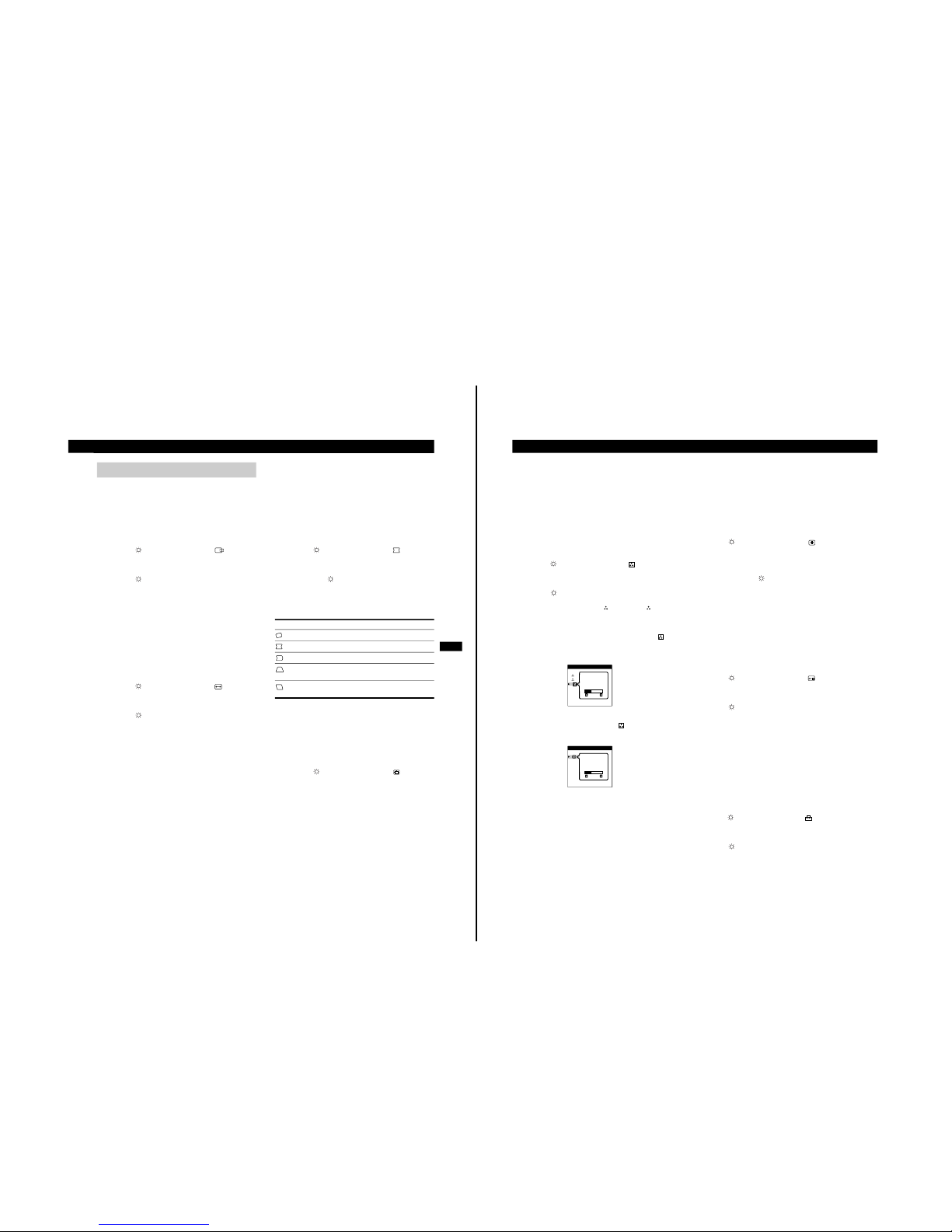
Introducing the OSD System
OK
MENU
MENU
EXIT
CENTER
SIZE
GEOMETRY
ZOOM
COLOR
CONVERGENCE
OSD POSITION
OPTION
GRAPHIC ENHANCEMENT
80.0kHz/ 75Hz
1280 X 1024
Horizontal/Vertical
frequencies for
current input signal
Resolution for current
input signal
1
CENTER
2
SIZE
3
GEOMETRY
4
ZOOM
5
COLOR
6
CONVERGENCE
7
OSD POSITION
8
OPTION
9 GRAPHIC ENHANCEMENT
CENTER
26
73
SIZE
26
73
ROTATION
GEOMETRY
26
ZOOM
ZOOM
COLOR
1
2
9300K
CONVERGENCE
26
73
OSD POSITION
26
73
MANUAL DEGAUSS
ON
OPTION
GRAPHIC ENHANCEMENT
STANDARD MODE
GRAPHICS/VIDEO MODE
PRESENTATION MODE
Page 7
— 7 —
VX900T
7
Customizing Your Monitor
US
1 Adjusting the centering of the
picture (CENTER)
This setting is stored in memory for the current input signal.
1
Press the MENU button.
The main MENU appears on the screen.
2
Press the
v/V
buttons to highlight CENTER
and press the MENU button again.
The CENTER menu appears on the screen.
3
Press the
v/V
buttons to adjust the vertical
centering, and the 6
B/b
buttons to adjust the
horizontal centering.
The OSD automatically disappears after about 30 seconds. To
close the OSD, press the MENU button again.
2 Adjusting the size of the picture
(SIZE)
This setting is stored in memory for the current input signal.
1
Press the MENU button.
The main MENU appears on the screen.
2
Press the
v/V
buttons to highlight SIZE and
press the MENU button again.
The SIZE menu appears on the screen.
3
Press the
v/V
buttons to adjust the vertical size,
and the 6
B/b
buttons to adjust the horizontal size.
The OSD automatically disappears after about 30 seconds. To
close the OSD, press the MENU button again.
3 Adjusting the shape of the
picture (GEOM)
The GEOMETRY settings allow you to adjust the rotation and
shape of the picture.
The rotation setting is stored in memory for all input signals. All
other settings are stored in memory for the current input signal.
1
Press the MENU button.
The main MENU appears on the screen.
2
Press the
v/V buttons to highlight GEOM and
press the MENU button again.
The GEOMETRY menu appears on the screen.
3
First press the v/V buttons to select the desired
adjustment item. Then press the 6 B/b buttons to
adjust the setting.
The OSD automatically disappears after about 30 seconds. To
close the OSD, press the MENU button again.
4
Enlarging or reducing the picture
(ZOOM)
This setting is stored in memory for the current input signal.
1
Press the MENU button.
The main MENU appears on the screen.
2
Press the v/V buttons to highlight ZOOM and
press the MENU button again.
The ZOOM menu appears on the screen.
3
Press the right 6 b button to enlarge the picture or th e
left 6 B button to reduce the picture.
The OSD automatically disappears after about 30 seconds. To
close the OSD, press the MENU button again.
Note
Adjustment stops when either the horizontal or vertical size reaches its
maximum or minimum value.
Adjusting the Settings
Select To
ROTATION
rotate the picture
PINCUSHION
expand or contract the picture sides
PIN BALANCE
shift the picture sides to the left or right
KEYSTONE
adjust the picture width at the top of the
screen
KEY BALANCE
shift the picture to the left or right at the
top of the screen
8
Customizing Your Monitor
5 Adjusting the color of the picture
(COLOR)
The COLOR settings allow you to adjust the picture’s color
temperature by changing the color level of the white color field.
Colors appear reddish if the temperature is low, and bluish if the
temperature is high. This adjustment is useful for matching the
monitor’s colors to a printed picture’s colors.
This setting is stored in memory for all input signals.
1
Press the MENU button.
The main MENU appears on the screen.
2
Press the
v/V
buttons to highlight COLOR and
press the MENU button again.
The COLOR menu appears on the screen.
3
Press the
v/V
buttons to select a color
temperature.
The preset color temperatures are 1 (9300K) and 2
(5000K). Since the default setting is 9300K, the whites change
from a bluish hu e to a reddish hue as th e temperature is lowered
to 5000K.
You can also fine tune t he color temperature by sele cting in
step 2 above, and using the 6 B/b buttons to adjust the color
temperature manually.
If you are using the Presentation or Graphic/Video mode, the
following COLOR OSD appears when “ COLOR” is
selected.
This OSD allows you to adjust the color temperature between
11,000K to 9,300K.
Press the 6 B/b buttons to adjust the color temperature.
The OSD automatically disappears after about 30 seconds. To
close the OSD, press the MENU button again.
6 Adjusting the quality of the
picture (CONV)
The CONV settings allow you to adjust the quality of the picture by
eliminating red or blue shadows around letters, characters and lines.
Both settings are stored in memory for all input signals.
1
Press the MENU button.
The main MENU appears on the screen.
2
Press the
v/V
buttons to highlight CONV and
press the MENU button again.
The CONVERGENCE menu appears on the screen.
3
Press the 6
B/b
buttons to adjust the horizontal
convergence, or the
v/V
buttons to adjust the
vertical convergence.
The OSD automatically disappears after about 30 seconds. To
close the OSD, press the MENU button again.
7 Adjusting the OSD position
(OSD)
This setting is stored in memory for the current input signal.
1
Press the MENU button.
The main MENU appears on the screen.
2
Press the
v/V
buttons to highlight OSD and
press the MENU button again.
The OSD POSITION menu appears on the screen.
3
Press the
v/V
buttons to adjust the vertical
position or the 6
B/b
buttons to adjust the horizontal
position.
The OSD automatically disappears after about 30 seconds. To
close the OSD, press the MENU button again.
8 Additional settings (OPTION)
You can manually degauss (demagnetize) the screen, lock the
controls, change the OSD language, restore the color image, and
cancel the moire.
1
Press the MENU button.
The main MENU appears on the screen.
2
Press the
v/V
buttons to highlight OPTION and
press the MENU button again.
The OPTION menu appears on the screen.
3
Press the
v/V
buttons to highlight the desired
adjustment item.
Adjust the selected ite m according to the following instructions.
The OSD automatically disappears after about 30 seconds. To
close the OSD, press the MENU button again.
VARIABLE
COLOR
1
2
VARIABLE
COLOR
Page 8
— 8 —
VX900T
9
Customizing Your Monitor
US
Degaussing the monitor
The monitor is automatically degaussed (demagnetized) when the
power is turned on.
To manually degauss the monitor, first press the
v/V
buttons to highlight (MANUAL DEGAUSS).
Then press only the right 6 b button.
The monitor is degaussed for about three seconds. If a second
degauss cycle is needed, allow a minimum interval of 20
minutes for the best result.
Locking the controls
To protect adjustment data by locking the controls,
first press the
v/V
buttons to highlight
(CONTROL LOCK). Then press the right 6 b button to
turn the lock ON.
Only the 1 (power) switch, EXIT and (CONTROL
LOCK) of the OPTION menu will operate. If any other
items are selected, the mark appears on the screen.
To cancel the control lock
Repeat the procedure above and set (CONTROL LOCK) to OFF.
Changing the OSD language
To change the language of the OSD, first press the
v/V
buttons to highlight (LANGUAGE). Then
press the 6
B/b
buttons to select the desired
language.
• ENG: English
• FRA: French
•DEU: German
• ESP: Spanish
•ITA: Italian
• NLD: Dutch
• SWE: Swedish
• RUS: Russian
• JPN: Japanese
Restoring the Color Image
The color of most display monitors tend to gradually lose brilliance
after several years of service. The Color Return featur e al lo ws you
to restore the color to the original factory preset levels.
To restore the image, first press the
v/V
buttons
to select (COLOR RETURN). Then press the right
6 b
button.
A white rectangle appears in the center of the screen while the
image is being restored (about two seconds).
Note
• Before using this feature, the monitor must be in normal operation mode
(Green power indicator) for at least 30 minutes. If the monitor goes into
power saving mode, you must return the monitor to normal operation
mode and wait for 30 minutes for the monitor to be ready. You may need
to adjust your computer’s power saving settings to help keep the monitor
in normal operation mode for the full 30 minutes. If the monitor is not
ready, the following message will appear.
• The monitor may gradually lose its ability to perform this function due to
the natural aging of the picture tube.
Cancelling the moire
To turn the moire cancellation function on or off, first
press the
v/V
buttons to highlight (CANCEL
MOIRE). Then press the 6
B/b
buttons to turn the
moire cancellation ON or OFF.
Adjusting the amount of the moire cancellation
Before you can adjust this s ettin g, the Cancel Moire setting must be
turned ON.
To adjust the amount of moire cancellation, first press
the
v/V
buttons to highlight (MOIRE ADJUST).
Then press the 6
B/b
buttons to adjust the amount of
moire cancellation until the moire effect is at a
minimum.
* Moire is a type of natural interference which produces soft, wavy lines on
your screen. It may appear due to interference between the pattern of the
picture on the screen and the phosphor pitch pattern of the monitor.
• ENG
• DEU
• ITA
• SWE
• JPN
LANGUAGE
• FRA
• ESP
• NLD
• RUS
OPTION
COLOR
RETURN
OPTION
ON
COLOR
RETURN
AVAILABLE
AFTER
WARM UP
OPTION
Example of moire
10
Customizing Your Monitor
9 Using the GRAPHIC
ENHANCEMENT OSD
This setting is stored in memory for the current input signal.
1
Press the MENU button.
The main MENU appears on the screen.
2
Press the
v/V
buttons to highlight GRAPHIC
ENHANCEMENT and press the MENU button again.
GRAPHIC ENHANCEMENT OSD appears.
3
Press the v button to select the mode.
The STANDARD MODE is ideal for spreadsheets, word
processing, and other text oriented applications.
The PRESENTATION MODE is useful for presentation programs
that require vivid colors.
The GRAPHICS/VIDEO MODE gives movies and games
enhanced visual appeal by increasing the sharpness and brightness.
The selected mode indication appears on the screen for about three
seconds.
If the screen appears too white, adjust the color temperature
(see “Adjusting the color of the picture (COLOR)” on page8).
Note
The PRESENTATION MODE and GRAPHICS/VIDEO MODE may
produce ghost images when displaying text oriented applications. These
modes change the brightness of the picture dynamically according to
changes in moving pictures. If ghost images appear, set the Video
Enhancement Mode to STANDARD MODE.
Resetting the adjustments
Navigate through the on-screen menus to sele ct th e adjustment it em
you want to reset, and press the RESET button. You can do this
while you are adjusting an item.
Press the RESET button when no menu is displayed on the screen.
Note that the following items are not reset by this method:
• on-screen menu language (page 9)
• on-screen menu position (page 8)
• control lock (page 9)
Press and hold the reset button for more than two seconds when no
menu is displayed on the screen. This resets everything to the
factory preset mode.
Press and hold the reset button for more than five seconds. This resets
everything to the factory presets including the input selection.
Note
The RESET button does not function when
(CONTOL LOCK) is
set to ON.
STANDARD MODE
PRESENTATION MODE
GRAPHICS/VIDEO MODE
Resetting a specific adjustment
Resetting all of the adjustments
for the current input signal
Resetting all of the adjustments
for all input signals
Resetting all of the adjustment
data to the factory presets
Page 9

— 9 —
VX900T
11
Technical Features
US
Specifications
Picture tube 0.25 – 0.27 mm aperture grill pitch,
19 inches measured diagonally,
90 degree deflection
Viewable image size Approx. 365 × 274 mm (w/h)
(14
3
/8 × 10 7/8 in.)
18.0" viewing image
Resolution
Horizontal Max. 1600 dots
Vertical Max. 1200 lines
Display picture size Approx. 352 × 264 mm (w/h)
(13
7
/
8
× 10 1/2 in.)
Deflection frequency
Horizontal 30 to 96 kHz
Vertical 48 to 120 Hz
AC input voltage/current 100 to 240 V, 50/60 Hz, 1.7 A
220 to 240 V, 50/60 Hz, 1.2 A
Dimensions
Approx. 444 × 467 × 455 mm (w/h/d)
(17 1/2 × 18 1/2 × 18 in.)
Mass Approx. 26 kg (57 lb 5 oz)
Plug and Play DDC/DDC2B, DDC2Bi, GTF
Design and specifications are subject to change without notice.
Monitor Information
You can display the model name, serial number and year of
manufacture using the INFORMATION OSD.
Press and hold the MENU button for 5 seconds.
The INFORMATION OSD appears.
The INFORMATION OSD includes the model name, serial number
and year of manufacture.
The OSD automatically disappears aftrer about 30 seconds.
Power Saving Function and
LED Indicators
This monitor has three Power Saving modes. By sensing the
absence of a video signal from the computer, it reduces power
consumption as follows.
If thin lines appear on your
screen (damper wires)
The lines you may be seeing on your screen are normal for the
Trinitron monitor and are not a malfunction. These are shadows
from the damper wires that stabilize the aperture grille, and are most
noticeable when the screen’s background is light (usually white).
The aperture grille is the essential element that makes a Trinitron
picture tube unique by allowing more light to reach the screen,
resulting in a brighter, more detailed picture.
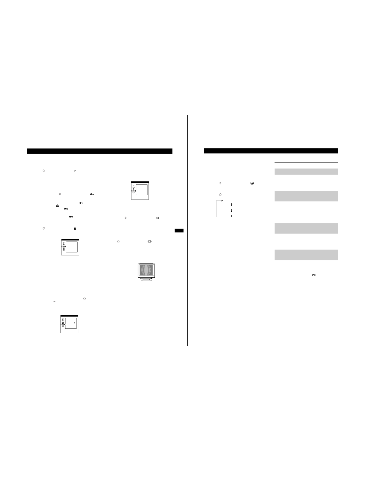
SER NO : 1234567
MODEL : CPD VX900T
MANUFACTURED
: 1998-53
INFORMATION
Power
consumption
mode
Power
consumption
Recovery
time
1
indicator
1Normal
operation
≤ 125 W — Green
2Standby
(1st mode)
≤ 15 W Approx.
3 sec.
Green and
orange
alternate
3Standby
(2nd mode)
≤ 15 W Approx.
3 sec.
Green and
orange
alternate
4 Active-off
(3rd mode)
≤ 8 W Approx.
10 sec.
Orange
5Power-off 0.2 W — Off
Damper wires
Approx. 7 cm
Approx. 7 cm
12
Additional Information
Warning Messages
If there is something wrong with the input signal, one of the following messages appears.
To solve these problems, see the “Troubleshooting” section below.
Troubleshooting
Before calling service technician regarding picture quality related questions, please press and hold (RESET) button for 6 seconds. This
resets everything to the factory presets including the input selection.
If the problem is caused by the connected computer or other equipment, please refer to the connected equipment’s instruction manual.
1
Out of Scan Range
This message indicates that the current input signal is not appropriate by the monitor’s specificatons.
2
Check signal cable (self test pattern)
This message indicates that there are no input signal is received, or the video cable is not connected.
Symptom Check these items
No picture
If the 1 (power) indicator is not lit • Check that the power cord is properly connected.
• Check that the 1 (power) switch is in the “on” position.
If the CHECK SIGNAL CABLE
message appears on the screen, or if
the 1 (power) indicator is either
orange or alternating between green
and orange
• Check that the video signal cable is properly connected and all plugs are firmly seated in
their sockets.
• Check that the HD15 video input cable’s pins are not bent or pushed in.
xProblems caused by the connected computer or other equipment
• The computer is in power saving mode. Try pressing any key on the computer keyboard.
• Check that the computer’s power is “on.”
• Check that the graphic video board is completely seated in the proper bus slot.
If the OUT OF SCAN RANGE
message appears on the screen
xProblems caused by the connected computer or other equipment
• Check that the video frequency range is within that specified for the monitor. If you replaced
an old monitor with this monitor, reconnect th e old monitor and adjust the frequency range to
the following:
Horizontal: 30–96 kHz
Vertical: 48–120 Hz
Picture flickers, bounces,
oscillates, or is scrambled
• Isolate and eliminate any potential sources of electric or magnetic fields such as other
monitors, laser printers, electric fans, fluorescent lighting and televisions.
• Move the monitor away from power lines or place a magnetic shield near the monitor.
• Try plugging the monitor into a different AC outlet, preferably on a different circuit.
• Try turning the monitor 90° to the left or right.
xProblems caused by the connected computer or other equipment
• Check your graphic video board manual for the proper monitor setting.
• Confirm that the graphics mode (VESA, VGA, etc.) and the frequency of the input signal are
supported by this monitor (Appendix). Even if the frequency is within the proper range,
some graphic video boards may have a sync pulse that is too narrow for the monitor to sync
correctly.
• Adjust the computer’s refresh rate (vertical frequency) to obtain the best possible picture.
INFORMATION
MONITOR IS WORKING
OUT OF SCAN RANGE
INFORMATION
MONITOR IS WORKING
CHECK SIGNAL CABLE
RED
GREEN
BLUE
WHITE
Page 10
— 10 —
VX900T
13
Additional Information
US
* If a second degauss cycle is needed, allow a minimum interval of 20 minutes for the best result. A humming noise may be heard, b ut this is not a malfunction.
Picture is fuzzy • Adjust the brightness and contrast (page 5).
• Degauss the monitor* (page 9).
• If CANCEL MOIRE is ON, the picture may become fuzzy. Decrease the moire cancellation
effect (page9) or set CANCEL MOIRE to OFF.
Picture is ghosting • Eliminate the use of video cable extensions and/or video switch boxes.
• Check that all plugs are firmly seated in their sockets.
• Check the Graphic Enhancement mode, if you are using a still picture application such as
Excel.
Picture is not centered or sized
properly
• Press the Auto Sizing and Centering button (page 5).
• Adjust the size (page 7) or centering (page7). Note that some video modes do not fill the
screen to the edges.
Edges of the image are curved • Adjust the geometry (page 7).
Wavy or elliptical pattern (moire) is
visible
• Cancel the moire (page 9).
x
Problems caused by the connected computer or other equipment
• Change your desktop pattern.
Color is not uniform • Degauss the monitor* (page 9). If you place equipment that generates a magnetic field, such
as a speaker, near the monitor, or if you change the direction the monitor faces, color may
lose uniformity.
White does not look white
• Adjust the color temperature (page 8).
Letters and lines show red or blue
shadows at the edges
• Adjust the convergence (page 8).
Monitor buttons do not operate • If the control lock is set to ON, set it to OFF (page 9).
COLOR RETURN does not function • COLOR RETURN does not work unless the monitor has been in normal operation (Green
power indicator) for at least 30 minutes. See page 9 for detailed information about Image
Restoration.
• In order to keep the monitor “on”, you may need to check the PC’s power saving setting.
• The monitor may gradually lose its ability to perform this function due to the natural aging of
the picture tube.
A hum is heard right after the
power is turned on
• This is the normal sound of the auto-degauss cycle. When the power is turned on, the monitor
is automatically degaussed for three seconds.
Symptom Check these items
COLOR
RETURN
AVAILABLE
AFTER
WARM UP
OPTION
Page 11
SECTION 2
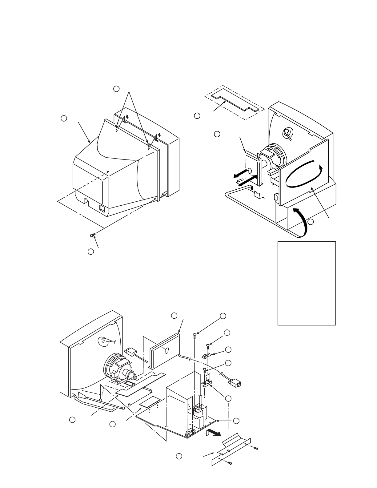
DISASSEMBLY
VX900T
2-1. CABINET REMOVAL
Two claws
3
Cabinet
2
Two screws
1
2-2. SERVICE POSITION
PUSH
PUSH
(BVTP 4 x 16)
2-3. D, A, H and N BOARD REMOVAL
A board
1
(additional board)
1
H board
2
Five screws
A board
3
(BVTP 3 x 12)
rotate 180º
3
D board
1 When the D-board is
placed in service
position, the Safety Earth
Wire (green and yellow
wire) is disconnected.
2 After service is
completed and the
D-board reinstalled, the
Safety Earth Wire must
be reattached to the
chassis with the proper
screw. This must be
confirmed before any
subsequent procedures
are attempted.
9
H board
2
N board
10
Holder
— 11 —
4
One screw
(BVTT 4 x 8)
5
Two Cable stoppers
6
Two screws
(BVTP 3 x 12)
7
Cable bracket
8
D board
Page 12

VX900T
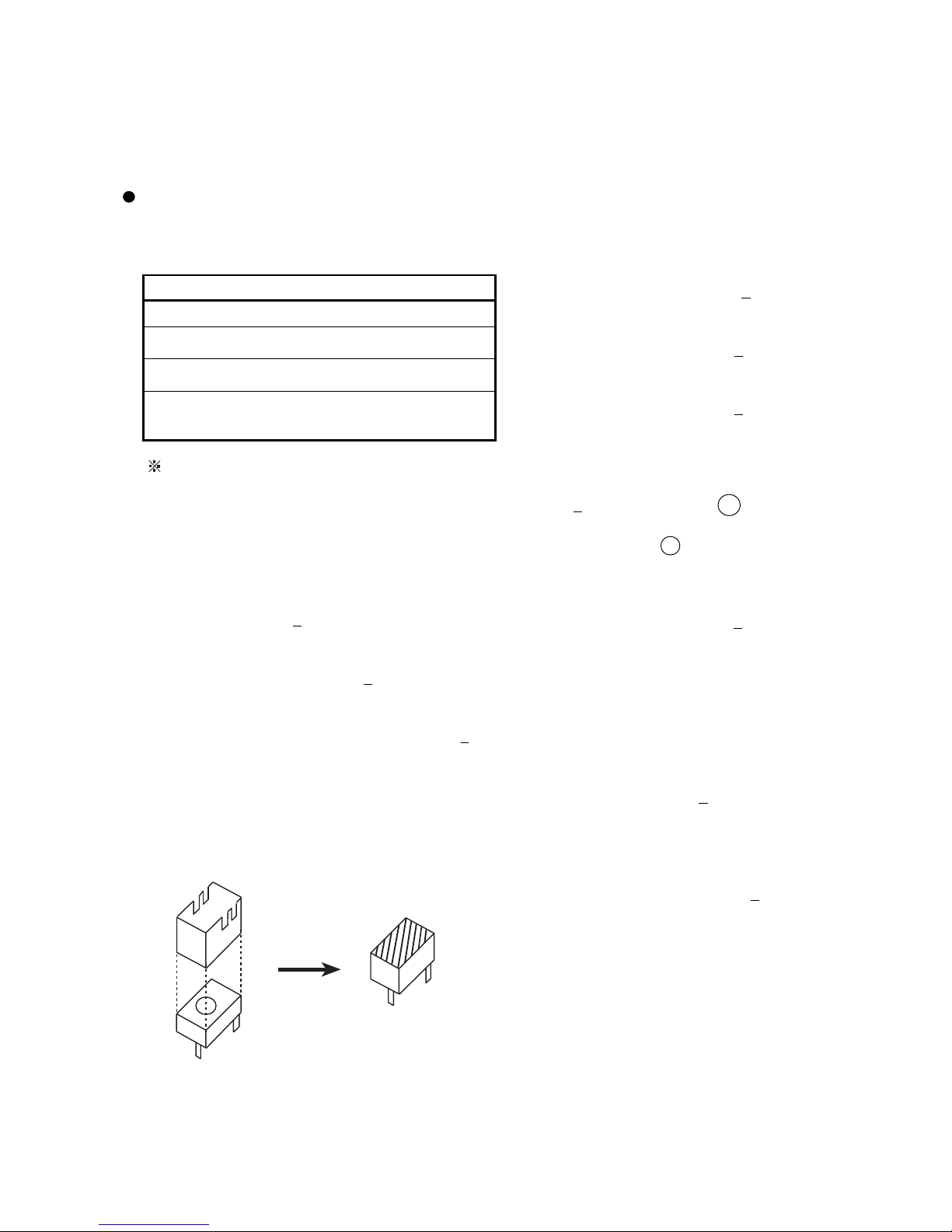
2-4. PICTURE TUBE REMOVAL
Demagnetization coil
7
Tension spring
6
A board
5
Neck assy
4
Deflection yoke
3
Four screws
(Tapping screw 5)
Picture tube shield
2
8
9
Two screws
(BVTP 4 x 16)
10
Stand assy
(D board)
1
Anode cap
Cushion
REMOVAL OF THE ANODE-CAP
NOTE: Short circuit the anode of the picture tube and the anode cap to the metal chassis, CRT shield or carbon painted on the CRT, after
removing the anode.
REMOVAL PROCEDURES
Turn up one side of the rubber cap in
the direction indicated by arrow .
Use your thumb to pull the rubber cap
firmly in the direction indicated by
arrow .
HOW TO HANDLE AN ANODE-CAP
Do not use sharp objects which may cause damage to the surface
of the anode-cap.
Do not squeeze the rubber covering too hard to avoid damaging
the anode-cap. A material fitting called a shatter-hook terminal is
built into the rubber.
Do not force turn the foot of the rubber cover. This may cause the
shatter-hook terminal to protrude and damage the rubber.
When one side of the rubber cap sepa-
rates from the anode button, the anodecap can be removed by turning the rubber cap and pulling it in the direction of
arrow .
— 12 —
Page 13
SECTION 3
SAFETY RELATED ADJUSTMENT
VX900T
When replacing parts shown in the table below, the
following operational checks must be performed as a
safety precaution against X-ray emissions from the unit.
D - BOARD
Part Replaced ([)
Part Replaced (])
T901, R903, IC805, R921, R922, R812, D908, IC605,
R913, R914, D802, D909
Allow the unit to warm up for one minute prior to
checking the following conditions:
RV904
a) HV Regulator Check
1) Input white cross hatch signal. (fH = 94 kHz)
2) Minimum CONT and BRT controls.
3) Cut off Screen VR (G2).
4) Input voltage: 120
5) Confirm that the voltage is within the voltage range
shown below.
Standard voltage: 27.0KV
6) When replacing components identified by ], make
sure to recheck the High Voltage.
7) Verify the High Voltage as shown above (27.0KV
is within specification. If not, set H. SIZE data at
minimum (-127) and then adjust RV904 on "D" Board.
8) After adjusting the High Voltage within specification,
put the RV cover on RV904 as shown below and apply
sufficient amount of RTV around RV904.
+ 2 VAC
+ 0.2KV
+ 0.2KV)
b) HV Hold-Down Check
1) Using an external DC Power supply, apply the voltage
shown below between cathode of D908 on "D" Board
and GND, and confirm that the HV Hold-Down circuit
works. (Raster disappears)
Apply DC Voltage: 21.5
Check Condition
• Input voltage : 120 + 2 VAC
• Input signal : (fH = 94 kHz), White Cross Hatch
• Controls : CONT (max) & BRT (center)
• B+ Voltage : 181
c) Beam Protector Check (Software logic)
1) Using an external current source, apply 1.30
+ 0.05 mA between pin 11 of FBT
(T501) and GND, and confirm that the voltage
at CN801 pin 1 is 2.25 VDC or less.
Check Condition
• Input voltage : 120
• Input signal : (fH = 94 kHz), White Cross Hatch
• Controls : CONT (max) & BRT (center)
d) B+ MAX. Check
1) Input white cross hatch (fH = 94 kHz) signal.
2) CONT (max) & BRT (center)
3) Input voltage: 120
Note: Use NF power supply or make sure that
distortion factor is 3% or less.
4) Confirm that the voltage is within the voltage
range shown below.
Standard voltage: 181
+ 0.5 VDC
+ 4.0 VDC
+ 2 VAC
+ 2 VAC
+ 4.0 VDC
104
RV904
RV501
— 13 —
Page 14

VX900T
SECTION 4
ADJUSTMENTS
Connect the communication cable of the connector located on the D board on the monitor. Run the service software and
then follow the instructions.
IBM AT Computer
as a Jig
1-690-391-21
1
D-sub
(9 Pin [female])
*The parts above ( ~ ) are necessary for DAS adjustment.
mini Din
(8Pin)
1
A-1500-819-A
2
Interface Unit
3
4 Pin
3-702-691-01
3
Connector Attachment
To BUS CONNECTOR
4 Pin 4 Pin
Allow a 30 minute warm-up period prior to making the following adjustments:
Landing Rough Adjustment
1. Enter the full white signal.
2. Adjust the contrast to the maximum.
3. Input full green signal.
Convergence Fine Adjustment
Set DY four-pole magnet to mechanical center
before adjustment.
This should be prime mode.
4. Moving the DY backward, and adjust coarsely the purity
magnet sothat a green raster positions in the center of
screen.
5. Moving the DY forward, adjust so that an entire screen
6-pole Mg
becomes pure green.
6. Adjust the tilt of DY, and tighten lightly with a clamp.
NECK Assy
P.S Mg
P.S. Mg
XBV
XBV
DY CRT
Set the
finger
Mechanical
Center
• Landing Fine Adjustment
1. Place the set in the Helmholtz coil.
2. Enter a green signal only.
3. Degauss the entire screen with hand-degausser. Then auto-
degauss it.
4. Attach a wobbling coil to the specified position of CRT
neck.
5. Attach a landing adjuster sensor on the CRT.
6. Using a landing checker, adjust the DY position, purity,
tilt of DY.
7. Clamp the DY screw.
Clamping torque: 22
+ 2 kgcm (2.2+ 0.2 N.m)
• Convergence Rough Adjustment
1. All digital convergence data should be zero by MCP.
2. Enter the white crosshatch signal.
3. Adjust roughly the horizontal and vertical
convergence at four-pole magnet.
4. Adjust roughly HMC and VMC at six-pole
magnet.
— 14 —
4-pole Mg
1. Receive R.B. cross-hatch.
2 Adjust H.STAT and V.STAT at four-pole magnet.
4 Pole Magnet
2
1
2
1
R
1
B
R
2
1
2
+
1
2
R
B
R
B
R
B
B
2
+
1
R
B
Page 15
VX900T
2
7
0
4
615
3
9
8
12
11
YBH-B
YBH-T
CBH-RT
MBH-RT
APH-R
MBH-RB
CBH-RBCBH-LB
MBH-LB
APH-L
MBH-LT
CBH-LT
Adjust each misconvergence point in sequence.
H STAT
3. Receive White cross-hatch.
4. Adjust HMC and VMC at six-pole magnet.
< 6 Pole Magnet>
2
G
1
2
G
1
5. Receive R.B. cross-hatch.
6. Adjust H.TILT by swinging the DY neck right and left.
7. Adjust XCV with XCV core.
XCV movement
B
R
8. Adjust V.TILT with TLV VR.
TLV movement
B
R
R
B
B
R
R
B
9. Adjust Y.CROSS with YCH VR.
YCH movement
Convergence Specification
C
Horizontal and Vertical
0.25mm
B
A
A 0.24mm
B 0.30mm
0.30mm
C < 0.35mm
Focus adjustment
Adjust focus (V) and focus (H) for optimum focus.
Focus (V)
FBT
Focus (H)
11. Digital Convergence Adjustment
A. Horizontal Convergence
10. Paint lock the four-pole and six-pole Mg.
RB
VR Adjustment on DY
XCV
YCH
TLV
Zero Position NECK Ass'y
Purity 4-Pole Mg 6-Pole Mg
Vertical and Horizontal Position and Size
Specification
B
a
a
A
bb
a < 3.0 mm
b < 3.0 mm
A B
264 352
B. Vertical Convergence
V STAT-T
CCV-LT
0
MCV-LT
XBV-L
4
MCV-LB
8
12
2
V STAT
9
11
3
7
615
V STAT-B
Adjust each misconvergence point in sequence.
C. Repeat the procedure of A and B so that the
convergence of the whole screen is within the
specification.
CCV-RT
MCV-RT
XBV-R
MCV-RB
CCV-RBCCV-LB
— 15 —
Page 16

VX900T
NOTES:
— 16 —
Page 17

NOTES:
VX900T
— 17 —
Page 18

VX900T
NOTES:
— 18 —
Page 19

VX900T
5-2. CIRCUIT BOARDS LOCATION
D1
5-3. SCHEMATIC DIAGRAMS AND PRINTED WIRING BOARDS
Note:
•
All capacitors are in µF unless otherwise noted. pF: µµF
50 WV or less are not indicated except for electrolytic.
•
Indication of resistance, which does not have one for rating
electrical power, is as follows.
Pitch: 5 mm
Rating electrical power 1/4 W (CHIP: 1/10 W)
•
All resistors are in ohms.
• f : nonflammable resistor.
• F : fusible resistor.
• ∆ : internal component.
• p : panel designation and adjustment for repair.
• All variable and adjustable resistors have characteristic curve B,
unless otherwise noted.
• e : earth-ground.
• E : earth-chassis.
• The components identified by [ in this basic schematic
diagram have been carefully factory-selected for each set
in order to satisfy regulations regarding X-ray radiation.
Should replacement be required, replace only with the
value originally used.
•
When replacing components identified by ], make the necessary
adjustments by using RV904 ([) as indicated. (See page 13)
Note: The components identified by shading and
mark ¡
with part number specified.
are critical for safety. Replace only
• When replacing parts shown in the table below,
be sure to perform the safety related adjustment.
Part Replaced ([)
Part Replaced (])
T901, R903, IC805, R921, R922,
R812, D908, IC605, R913, R914,
D802, D909
• All voltages are in volts.
• Readings are taken with a 10 ΜΩ digital multimeter
• Readings are taken with a color-bar signal input.
• Voltage variations may be noted due to normal
production tolerances.
• * : Cannot be measured.
• Circled numbers are waveform references.
• : B +bus.
• : B - bus.
D - BOARD
RV904
Note: Les composants identifies per un trame et une
marque ¡ sont critiques pour la securite. Ne les
remplacer que par une piece portant le numero specifie.
— 22 —
Page 20

13
HV
17
14
15
16
11
12
FV1
FV2
4
1
2
6
8
10
9
7
5
1
2
3
4
5
6
7
1
2
3
4
5
6
7
8
1
3
4
5
6789
10
11
13
KR
KRKG
KB
G2
G2
G1
G3
H
H
RCV
1
2
3
4
5
6
7
8
9
10
11
12
13
14
15
16
17
18
19
20
21
22
23
24
25
26
27
28
29
30
1
2
3
4
5
6
7
8
9
10
11
12
13
14
15
16
17
18
19
20
21
22
23
24
25
26
27
28
29
30
A
G
1
2
6
7
8
9 10
11
12
13
14
15
16
17
18
3
4
5
1
2
3
4
5
6
7
8
1
2
3
4
5
6
7
8
9
1
2
3
4
5
1
2
3
4
1
1
2
3
4
5
6
7
8
9
1234567
1
2
5
6
9
7
1
2
2
3
4
5
7
9
10
11
12
124
3
L
G
N
1
2
3
124
3
D2001
T901
T503
D601
RY601
T701
T601
:FBT
:LCT
DEGAUSS
RELAY
:DFT
:SRT
1
2
3
4
5
6
7
8
9
1
23456
7
12345678
1
2
3
4
5
1234
1
2
12121
2
1
2
3
4
5678
9
10
11
12
1
1
2
3
4
5
6
7
8
9
1
2
3
4
5
6
7
8
9
10
11
12
13
14
15
16
17
18
19
20
21
22
23
24
25
26
27
28
29
30
1234567
1
2
3
4
5
6
7
8
9
10
11
12
13
14
15
16
17
18
19
20
21
22
23
24
25
26
27
28
29
30
1
2
12
12
1
23
12
1
2
3
4
5
6
7
8
910
11
12
13
14
15
16
17
18
1
2
4
5
6
7
8
9
10
11
12
13
14
15
16
17
12
12
1
2
1
2
1
2
3
4
5
6
7
8
1
2
12
1
2
1
2
1
2
1256
79
12
12
2
3
4
5
7
9
10
11
12
1
2
12
1212
12
3
4
1
2
1
2
1234
1
2
3
1212
1
2
3
12
34
5
6
1
2
1
2
1
23
412
12122
1
2
1
2
1
2
1
2
122
2
2
3
4
5
6789
10
11
13
1
4
2
21
43
65
B OSD
G OSD
R OSD
R OSD
G OSD
B OSD
R
G
B
G
R
BLK
CLAMP
CSYNC
B
L
K
C
S
Y
N
C
B
C
L
A
M
P
H
.
S
Y
N
C
V
.
S
Y
N
C
C
.
S
Y
N
C
B
P
C
L
A
M
P
I
N
P
U
T
S
W
INPUT SW
BP CLAMP
H.SYNC
V.SYNC
C.SYNC
S0
S1
S2
S3
S5
S5
S4
S3
S2
S1
YDC
XDC
DEGAUSS
HV.DET
PWR SHUT
HV.DET
PWR SHUT
DEGAUSS
H.CENT
H.LIN BAL
H.CENT
H.LIN BAL
D
D
C
C
L
K
D
D
C
D
A
T
A
TXD
RXD
RXD
TXD
YSC
XSC
COM BRT
COM CONT
COM CONT
LED2
LED1
LED2
DDCCLK
DDCDATA
COM BRT
LED1
S0
S1
S2
S3
S4
S5
XSC
YSC
C
O
M
B
R
T
C
O
M
C
O
N
T
L
E
D
2
L
E
D
1
KEY SCAN1
LED1
LED2
COM CONT
COM BRT
ROTATION
D TILT
D TILT
ROTATION
S0
YDC
XDC
XSC
YSC
YSC
XSC
TXD
RXD
TXD
RXD
B.GND1
BLUE1
G.GND1
GREEN1
R.GND1
RED1
GND
VD1
HD1
7
9
10
11
Q004Q002
8
9
4
IC006
30
12
18
HRTRC
IICSCL
IICSDA
HOST GND2
H
.
S
Y
N
C
NC
GND
V.SYNC
DDCSDA
DDCSCL
O
ST GND1
NC
NC
DDCSDA
DDCSCL
HOST GND1
NC
3
4
7
6
5
1
2
17 8
11
12
14
15
16
17
16
27
24
20
13
15
3
4
5
6
C
B
L
K
I
N
P
U
T
S
E
L
E
C
T
B
P
C
L
P
C
S
Y
N
C
V
S
O
U
T
G
N
D
H
S
Y
N
C
14
1
3
5
8
9
11
IC002
IC004
1
15
3
12
4
9
10
7
13
IC005 Q001
IC009
5
6
7
1.2KV
1 3
GND
+12V
H1
GND
NC
+80V
STBY+5V
NC
+180V
SDA
SCL
HFLY
VSYNC
HSYNC
ROUT
GOUT
BOUT
XTALIN
XTALOUT
AVFBLK
SDA
SCL
B_IN
G_IN
R_IN
CSYNC
CLAMP
BLK
R_OSD
G_OSD
B_OSD
BOUT
GOUT
ROUT
G2
B_BKG
G_BKG
R_BKG
OSD_BLK
V_DET
SYNC_IN
B_IN
B.F.B.
G_IN
G.F.B.
R_IN
R.F.B.
B_OUT
G_OUT
R_OUT
R_IN
G_IN
B_IN
R_OUT
G_OUT
B_OUT
+
-
OUT
DDCSCL
DDCSDA
HOST GND1
H
.
S
Y
N
C
V.SYNC
HRTRC
IICSCL
IICSDA
C
B
L
K
B
P
C
L
P
C
S
Y
N
C
V
S
O
U
T
H
S
Y
N
C
BLUE1
GREEN1
RED1
VD1
HD1
(VIDEO)
R
G
B
GND
GND
H.SHAPE
H.CENT
H. LIN BAL
S0
S1
S2
S3
S4
S5
REMOTE ON/OFF
PWR SHUTDOWN
ABL DET.
V.FBP
V.PIN
REF DC
HD OUT
DEGAUSS
HV. DET
GND
IK SIGMA
VSAWN
DCC2
DAC REF
NC
YDC
XDC
GND
GND
D
D
C
C
L
K
D
D
C
D
A
T
A
C
P
U
G
N
D
1
I
I
C
D
A
T
A
C
P
U
G
N
D
2
I
I
C
C
L
K
H
.
F
B
P
I
N
P
U
T
S
W
V
.
S
Y
N
C
G
N
D
H
.
S
Y
N
C
C
.
S
Y
N
C
B
P
C
L
A
M
P
C
.
B
L
A
N
K
V
.
S
Y
N
C
H
.
S
Y
N
C
G
N
D
.
A
G
N
D
.
A
1
2
3
4
1
1
1
0
9
8
7
6
5
+5V
ROTATION
KEY SCAN1
LED1
LED2
B+ DET.
TXD
RXD
HEATER
D.TILT
XSC
YSC
GND
GND
THERMAL
COM CONT
COM BRT
LCC RT
LCC LT
LCC RB
LCC LB
NC
GND
GND
GND
H.DF
H.FBP
GND
V.DF
GND.A
39
6
8
20
57
25
64
44
42
27
48
47
40
1
22
28
20
30
17
19
53
50
49
48
47
46
42
6
7
16
5
2
4
34
35
37
36
32
26
25
27
IC1001
IC1002
Q1002
Q1003
I O
5V
5V
5
6
6 7 1 2
3
1
5
2
7
33
21
3224
10
58
38
39
60
61
3
59
14
12
13
51
52
15
23 46
13
Q1001
5V
VCC OUT
PWM4/P4.4
P3.6/SIN
P3.5/SOUT
AIN0/P8.2
AIN1/P8.3
P8.6
P8.7
AIN3/P8.5
HSYNCO
WDOUT/INT2/P5.3
VSYNCO/P5.2
P5.0/HFBACK
P6.0/SDAI
P6.1/SCLI
P6.6/SDAD
P6.7/SCLD
P3.7/HSYNCI2
INTO/P5.7
VSYNCI2/
PMW3/P4.3
PWM5/P4.5
PWM2/P4.2
AIN4/P6.5
PWM1/P4.1
PWMN0/P4.0
P3.4/RXCLK
P3.2/TOUT/DCD
P3.3/BLANKOUT
P3.1/TOUTA/CTS
P8.0
P8.1
P3.0/TXCLK/CLKOUT
AIN0/VFBACK/P6.2
AIN5/P6.4
HSYNCI1
VSYNCI1
CSYNCI/P5.1
CLAMPOUT/MOIRE/P5
PWM6/P4.6
INT3/P5.4
WDIN/INT1/P5.5
VDF1
YSC
XSC
H-IN
V-IN
FBP-IN
SCL
SDA
POC-OUT
LOCK-DET
DCC
VDF2
V-FBP
XDC
YDC
PC2-FIL
TILT
H-OUT
HDF1
E/W
PC1-FIL
DCC2
VSAWN
BLK
AIN2/P8.4
1
2
3
4
5
6
7
8
9
10
11
12
13
14
15
16
17
18
19
20
21
22
23
24
25
26
27
28
29
30
1
2
3
4
5
6
7
8
9
10
11
12
13
14
15
16
17
18
19
20
21
22
23
24
25
26
27
28
29
30
1
2
3
4
5
6
7
8
9
1
1234567
8
GND
GND
LED1
LED2
GND
5V
COM CONT
COM BRT
THERMAL
KEY SCAN 1
123456789
10
123
4
123
4
F1NCNC
F1
S602
POWER ON
S2001-S2008
15
14
1328
Q801
Q504
Q508 - Q513
Q501 - Q503
IC701
IC805
2
3
4
5
6
1
11
Q802
IC605
3 1
Q601, 606, 607
IC604
I O
12
IC502
5
3
1
2
VC
IC704
7
4
6
3
Q515
Q517
Q516
3
1
7
6
4
4
T501
1
6
Q505
T504
2
1
3
3
Q518
K
E
Y
S
C
A
N
1
5V
S0-S5
IC401
Q902
31
Q901
18 19
Q706, 707
124
IC702
ROTATION-
ROTATION+14
1
2
8
9
CY1+
CY1-
CY2+
CY2-
CY3+
CY3-
CY4+
CY4-
1
2
3
4
5
6
H DY+
H DY+
H DY-
H DY-
V DY-
V DY+
Q507
6
IC703
4
T902
T502
25
Q514
Q506
20
11
1
IC601
46
729
IC603
DGC1
DGC2
NC
Q670
Q657
Q640
IC652
1 3
Q658
Q656
Q605
IC606
(POWER DEFLECTION)
D CONV
OUT
S CONV
OUT
V OUT
LF602
3214
STDBY
OUT A (X)
IN B -
IN A -
IN A +
IN B +
OUT B
I OUT B
OUT A
I OUT A
INPUT1DISABLE
SD
CCP
OUT
CLM
TR
VCC
OUT A (X)
STBY
+IN A (X)
B4+
OP2+
B10
H DRIVE
B20B30
REF
S4
IC1003
54
49
RESET
RESET
Q602
RESET
MICRO
DSP
PROTECT-2
JITTER KILLER
3.3V REG
H OUT PROTECT 1
IC1007
VSAW OUT
IC1005
EEPROM
IC003
OSD
IC001
SHARPNESS
PREAMP
RGB OUT
CUTOFF
AMP
CUTOFF
CTRL
SPOT KILLER
VOLTAGE
REGULATOR
CN305 CN602
CN510CN301
CN101 (1/2)
CN101 (2/2) CN801 (2/2)
CN801 (1/2)
FUNC SW
5V
V DF OUT
HV OUT
ROTATION
HRC
OUT
HV REG
HOC
H RTRC
H OUT
HST
BUFFER
HDT
5V STBY BACKUP
12, 5V REG
SPOT KILLER
H DRIVE
REG OUT
H SIZE
STBY
MUTE
REG CTRL
HV/H SIZE
H DRIVE BUFF
H DF OUT
+IN A (X)
OUT B (Y)
-IN A (X)
+IN B (Y)
-IN B (Y)
S CAP SW
POWER SW
POW SUPP
CTRL
OUT
H CENT
AMP
ERROR
SELV-SHORT
CKT PROT
OVP/OCP
FLT PROT
STBY MODE OCP ENABLE
CN2001
CN1001
CN2003
CN603
CN1003
CN1004
CN309CN306
CN311
CN310
CN313
CN501
CN601
CN600
CN702
CN701
5V
300V
5V
STBY+5V
+12V
+80V
+180V
5V OUT
+180V
+80V
+12V
STBY+5V
5V IN 5V OUT
5V
CN901
1
2
3
4
D GND
+5V
RXD
TXD
5V
FOR SERVICE
IC1006
TO CRT HV
(MICRO, DSP)
(FUNC CTRL)
12V IN
5V
-16V
16V
80V
180V
HORIZ CTR CTRL STBY SW
BUFF
HCL CTRL
LFT
H DRIVE
BUFFER
H DRIVE/BUFFER
STBY CTRL
OCP
ENABLE
CTRL
DEG SW
B-SV9162<MAUAL>-BLK..
Page 21

1
3
4
5
6789
10
11
13
KR
KRKG
KB
G2
G2
G1
G3
H
H
RCV
1234567891011
1
2
3
4
5
6
7
8
1
2
3
4
5
6
7
1 2 3 4 5 6 7 8 9 10 11 12 13 14 15
1
2
3
4
5
6
7
8
9
1
0
1
1
1
2
1
3
1
4
1
5
1
6
1
7
1
8
1
9
2
0
2
1
2
2
2
3
2
4
2
5
2
6
2
7
2
8
2
9
3
0
1
2
3
4
5
6
7
8
1
2
3
4
5
6
7
8
1
0
9
1
1
1
2
1
3
1
4
1
5
1
6
1
7
1
8
1
9
2
0
2
1
2
2
2
3
2
4
1 2 3 4 5 6 7
891011121314
123
1
1
2
3
4
1
2
3
4
5
6
7
8
9
1
2
3
4
5
1
2
3
4
5
6
7
8
9
FB012
R017
R018
R021
R020
R
2
0
4
R104
R207
R307
R106
R206
R306
J001
R351
R251
R151
R109
R
2
0
9
R309
R048
R064
SG001
SG201
SG101
SG301
R053
R031
R045
R029
IC002
C305
C205
C105
CN302
CN303
IC005
FB009
FB010
FB101
FB201
FB301
FB110
FB310
F
B
2
1
0
C104
C204
C304
C010
C001
C013
C012
C092
R304
C020
C022
R030
CN309
C004
C053
R046
R047
D007 D008
L301
L201
L101
R233
C090
IC004
R205
R305
IC001
R111
R211
R311
C352
D311
D211
D111
D002
D003
C252
C152
R330
C019
C119
C330
C130
C108
C208
C308
D005
JW301
JW201
JW101
C033
CN306
R115
R215
R315
IC003
C046
C038
C037
R033
R034
IC006
FB104
R117
R217
R317
SG002
C041
FB015
FB016
FB017
FB018
FB019
FB020
R318
R218
R118
C049
IC009
D022
C121
C221
C321
D120 D220 D320
C
0
5
9
C058
C057
C122
C222
C322
Q004
L003
R060
R019
R004
R310
R210
R
1
1
0
F
B
3
1
1
F
B
2
1
1
FB111
CN308
R014
R006
C015
D304
D204
D305
D205
C014
D106
D206
D306
C
0
1
8
CN301
C035
Q001
D014
C028
F
B
0
0
1
FB005
FB011
FB006
R049
C029
FB004
C054
C306
C106
C031
C027
C009
C016
D105
D104
CN310
R108
R208
R308
CN305
R001
R009
R025
R105
R107
R116
R316
R216
R361
R261
R161
R011
R013
R012
D015
D004
R007
R130
R230
C040
C109
R022
R023
C319
C039
R032
JW202
JW102
C011
C044
C045
C043
FB002
C042
FB302
FB202
FB102
C230
R024
D108 D208 D308
R122
R222
R322
R319
R320
R119
R120
R220
R219
C055
X001
C007
R054
Q002
R056
C062
R058
C060
CN311
CN313
D
0
2
3
D024
D025
C
2
1
1
C111
C311
L004
D309
D209
D109
C061
FB014
R112 R212
R312
C206
100:CHIP
100:CHIP
100:CHIP
100:CHIP
6
8
:
C
H
I
P
68
:CHIP
1.0k
:CHIP
1.0k
:CHIP
8.2k
:CHIP
8.2k
:CHIP
8.2k
:CHIP
100
1/2W
:RC
100
1/2W
:RC
100
1/2W
:RC
1M
:CHIP
1
M
:
C
H
I
P
1M
:CHIP
2.2M
1W
:RN
10k
1/2W
:RC
22M
:RN
1k
:CHIP
2.2k
:CHIP
120k
:CHIP
LM2403
RGB OUT
0.1
25V
B:CHIP
0.1
25V
B:CHIP
0.1
25V
B:CHIP
CUTOFF CTRL
0.1
25V
B:CHIP
0.1
25V
B:CHIP
0.1
25V
B:CHIP
0.1
25V
B:CHIP
0.001
500V
47
25V
0.001
:CH
0.1
25V
B:CHIP
68
:CHIP
470
16V
47
25V
100
:CHIP
7P
WHT
:S-MICRO
0.01
B:CHIP
0.1
25V
B:CHIP
100k
:CHIP
10k
:CHIP
MTZJ-T-77-5.6B MTZJ-T-77-5.6B
27
27
33
:CHIP
0.01
B:CHIP
STV5109
CUTOFF AMP
220k:RN
220k:RN
CXA2066S
SHARPNESS/PREAMP
82
:PFRD
100
:FPRD
100
:FPRD
100
16V
1PS226-115
:PROT
1PS226-115
:PROT
1PS226-115
:PROT
1SS119
1SS119
100
16V
100
16V
56
:CHIP
0.01
B:CHIP
0.01
B:CHIP
0.22
16V
B:CHIP
0.22
16V
B:CHIP
0.1
25V
B:CHIP
0.1
25V
B:CHIP
0.1
25V
B:CHIP
1SS119
(7.5MM)
(12.5MM)
(12.5MM)
0.1
25V
B:CHIP
8P WHT :S-MICRO
270k
270k
270k
SNY432
OSD
0.01
0.001
B:CHIP
0.047
F
2.2k
:CHIP
22k
:CHIP
SN74HCT02ANS-E20
H DRIVE
BUFFER
10
:CHIP
47
:CHIP
47
:CHIP
0.001
500V
B
47
:CHIP
47
:CHIP
47
:CHIP
0.1
25V
B:CHIP
NJM78M05FA
VOLTAGE REG
1SS119
0.1
25V
B:CHIP
0.1
25V
B:CHIP
0.1
25V
B:CHIP
1SS119 1SS119 1SS119
0
.
1
2
5
V
B
:
C
H
I
P
22p
CH
68p
CH:CHIP
0.1
25V
0.1
25V
B:CHIP
0.1
25V
2SC1623-L5L6
H DRIVE
180
2.7k
:CHIP
1.0
:CHIP
8.2k
:CHIP
8.2k
:CHIP
8
.
2
k
:
C
H
I
P
4.7k:CHIP
100:CHIP
0.1
25V
B:CHIP
HSS82
HSS82
HSS82
HSS82
47
100V
HSS82
HSS82
HSS82
1
0
2
0
0
V
1P
470p
2kV
B
2SC5022
SPOT KILLER
1SS119
47
25V
68k
:CHIP
0.1
25V
B:CHIP
0.1
250V
:MPS
0.47
250V
:MPS
0.47
250V
:MPS
0.001
500V
B
0.01
1000
25V
470
16V
HSS82
HSS82
4P
WHT
:S-MICRO
1.0k
:RN
1.2k
:RN
1.2k
:RN
9P
WHT
:S-MICRO
4.7k
:CHIP
10k
:CHIP
4.7k
:CHIP
220k
:RN
1.0k
:CHIP
15k
15k
:RN
15k
:RN
75
:RN
75
:RN
75
:RN
10k
:CHIP
100
:CHIP
10k
:CHIP
1SS119
1SS119
100
:CHIP
56
:CHIP
56
:CHIP
0.01
B:CHIP
47
25V
100
:CHIP
1k
:CHIP
0.01
B:CHIP
0.1
100V
100:CHIP
(12.5)
(22.5MM)
0.1
100V
:PT
0.001
500V
B
0.1
25V
0.1
25V
0.1
100V
0.22
16V
B:CHIP
4.7k
:CHIP
1SS119 1SS119 1SS119
82
:RN
82
:RN
82
:RN
47k
47k
47k
47k
47k
47k
22p
CH
10
1k
:CHIP
2SA1162-G
BUFFER
2.2k
:CHIP
10p
:CHIP
470
:CHIP
4.7
5P
WHT
:S-MICRO
9P
WHT
:S-MICRO
M
T
Z
J
-
T
-
7
7
-
6
.
2
MTZJ-T-77-3.6B
MTZJ-T-77-6.2
0
.
0
2
2
B
:
C
H
I
P
0.022
B:CHIP
0.022
1SS83RE
1SS83RE
1SS83RE
0.22
16V
JW(5.0MM)
47k
47k
47k
0.47250V:MPS
+12V
+
1
2
V
+
8
0
V
STBY+5V
12V
STBY+5V
STBY+5V
STB+5V
S
T
B
Y
+
5
V
STBY+5V
+
1
8
0
V
2
3
4
5
6
78
9
10
11
13
1
3
2
GND01
V
B
I
A
S
G
N
D
3
V
C
C
G
N
D
2
G
N
D
1
GND
+12V
H1
GND
NC
CSYNC
VSOUT
GND
HRTRC
DDCSDA
DDCSCL
D
D
C
S
D
A
D
D
C
S
C
L
1.2KV
+80V
STBY+5V
IICSCL
IICSDA
CBLK
BPCLP
HSYNC
NC
INPUT SELECT
HOST GND2
HOST GND1
H
O
S
T
G
N
D
1
B.GND1
BLUE1
G.GND1
GREEN1
R.GND1
RED1
GND
VD1
HD1
B
.
I
N
G
.
I
N
R
.
I
N
R
.
O
U
T
G
.
O
U
T
B
.
O
U
T
B
.
I
N
V
C
C
.
L
G
.
I
N
R
.
I
N
V
C
C
.
M
R
.
B
.
C
.
F
.
R
.
O
U
T
G
N
D
R
.
F
.
B
.
G
.
O
U
T
G
.
B
.
C
.
F
.
B
.
O
U
T
B
.
B
.
C
.
F
.
B
.
F
.
B
.
G
.
F
.
B
.
+ GND
-
OUT
VCC
SDA
SCL
G2
G BKG
+5V
SYNC IN
CLAMP
G OSD
C. SYNC
ABL
G GND
G OUT
BLK
OSD BLK
V DET
S/H G
H.SYNC
NC
GND
V.SYNC
NC
N
C
+180V
+12V
N
C
B IN
R IN
B BKG
R BKG
G IN
R GND
R OUT
S/H R
B GND
B OUT
S/H B
FILT
GND
SDA
SCL
HSYNC
VSYNC
HFLY
AV
VDD_D
VSS_D
XTALIN
XTALOUT
OSCREF
ADCREF
RCI
GCI
BCI
VCC
VDD_IO
FBLK
BOUT
GOUT
ROUT
VSS_IO
B OSD
R OSD
TO D BOARD
CN510
TO D BOARD
CN602
TO INPUT
SIGNAL
TO N BOARD
CN1004
TO N BOARD
CN1003
(VIDEO)
CN1003
TO N BOARD
SIGNAL IN
TO
3
A
3
B
3
Y
2
A
2
B
2
Y
B-SV9162<MANUAL>-A..
STBY+5V
+12V
+80V
+180V
+12V
STBY+5V
STBY+5V
STBY+5V
STBY+5V
STBY+5V
+12V
1
2
3
4
5 6
7
8 9
10
11
12
Page 22

18 0.54
19 GND
20 2.54
21 3.66
22 11.81
23 GND
24 2.45
25 3.65
26 GND
pin volt
1 54.20
2GND
3 55.50
4GND
5 53.80
6 77.80
7GND
82.52
12.99
2GND
34.69
44.33
50.47
60.04
70.00
80.03
95.03
A BOARD WAVEFORMS
1 2 3
15 0.00
16 0.01
17 0.01
18 3.79
19 5.03
20 0.91
21 0.96
22 1.02
23 3.41
33.78
43.80
5182.30
61.13
7103.40
8GND
9100.90
10101.10
11 1.35
pin volt
1N.C.
2GND
3GND
4GND
53.21
63.24
710.92
8 11.89
44.80
50.29
60.29
7GND
84.03
94.03
10 0.29
11 GND
12 GND
3N.C.
4GND
54.58
64.59
70.00
85.03
IC008
15.02
21.42
84.48
90.00
10 GND
11 1.42
12 0.00
13 1.42
14 0.00
15 0.00
16 1.42
22 4.52
36 5.02
23 GND
24 5.02
25 N.C.
26 GND
27 2.09
pin volt
I 11.89
GGND
O5.03
28 5.02
29 GND
30 2.07
All voltages are in V
4.66V
(H)
p-p
4.37V
(H)
p-p
4 5 6
52.50V
p-p
(H)
38.75V
p-p
(H)
7 8 9
48.13V
p-p
(H)
38.13V
p-p
(H)
100.0 VDC above GND
10 11 12
4.37V
38.44V
51.88V
p-p
p-p
p-p
(H)
(H)
(H)
p-p
(H)
0.76V
0.76V
(H) 0.76V
p-p
p-p
(H)
Page 23

HV
1
2
14
13
17
16
11
6
5
4
8
912
FOCUS
1
2
3
4
5
6
7
8
9
1
0
1
1
1
2
1
3
1
4
1
5
1
6
1
7
1
8
1
9
2
0
2
1
2
2
2
3
2
4
2
5
2
6
2
7
282
9
3
0
3
1
3
2
3
3
3
4
3
5
3
6
3
7
3
8
3
9
4
0
4
1
4
2
4
3
4
4
4
5
4
6
4
7
4
8
4
9
5
0
5
1
5
2
5
3
5
4
5
5
5
6
S
1
3
4
5
6 7
8
9
10
11
12
1
2
346
7
8
S
S
1
2
5 6
10
9
4
1
2
3
4
1
2 3
4
1
2
3
4
5
6
7
8
9
1
0
1
1
1
2
1
3
1
4
1
5
1
6
1
2
3
4
5
6
7
1
2
3
1
2
43
5
6
1
2
3
4
5
6
7
8
9
1
0
1
1
1
2
1
3
1
4
1
5
1
6
1
7
1
8
1 2 3 4 5 6 7 8 9 10 11 12 13 14 15
1234
5 6 7 8
1
2
3
4
5
6
7
8
9
10
1
2
1
12
3
1
2
3
4
5
6
7
8
9
1
0
1
1
1
2
1
3
1
4
1
5
1
6
SS
S
12345
1
2
S S
12345
S
1
2
3
4
5
6
1
2
3
L
G
N
1
2
3
5
6
7
8
9 10
11
12
13
14
15
16
17
18
4
1
2
3
4
5
6
7
8
9
1
0
1
1
1
2
1
3
1
4
151
6
1
7
1
8
1
9
2
0
2
1
2
2
2
3
2
4
2
5
2
6
2
7
2
8
2
9
3
0
1 2 3 4 5 6 7
1
2
3
4
5
6
7
8
15
23
4
1 2 3 4 5 6 7 8 109 11 12
131415161718192021222324
1
2
3
4
5
6
7
S
1
2
3
4
5
6
7
8
9
1
2
3
4
5
6
1
23
CN512
R519 R524
R520
D504
SG501
C541
R543
C547
R566
R563
R557 C548
R513
T503
R508
C503
C512 C515
C520
RV501
C509
C910
R604
C614
D
9
0
6
CN601
R906
C404
C913
C903
C902
C615
C926
C703
C705
L603
L604
R728
R729
R717
R718
R922
CN902
C930
R634
C712
D916
D914
D908
D
9
0
5
D907
C908
RY601
R619
R615
R617
CN501
R401
C402
R402
R915
R603
C925
C708
C711
C920
C921
CN701
C911
C929
R633
R624
R532
R625
D618
D617
R523 R535 R537
R510
R577
C536
C538
R500
R504
C551
C552
R574
R511
D608
D901
R614
R569
R941
R943
R944
LF602
TH601
TH600
C403
R957
R958
C624
C633
R580
R613
R567
R515 R521
R525 R533
R536
C550
C928
C927
C704
RY500
R529
T504
C406
C502
C517
C544
C914
R404
R501
R509
R512
R522
R527
R528
R540
R541
R547
R549
R560
R562
R705
R706
R708
R709
R727
R940
C637
C630
R620
C501
C613
C618
C915
D909
D910
C516
R538
R544
C549
C526
C519
R542
R564
C532
R534
R909
R908
D
5
2
4
D525
C522
R526
CN503
R403
R405
R583
R558
D611
R927
C912
C558
R611
R539
C563
CN502
C510
C561
L501
R561
R530
R531
C553
C554
C570
C576
D704
C905
C906
R931
C924
R571
C580
R600
CN901
L510
R710
R934
R576
R942
R946
R553
R568
R945
CN903
C559
R570
R581
R707
R719
R572
R579
R573
C507
TH501
D918
D919
C916
R623
C709
C710
C557
R407
R408
C405
C543
R587
R505
R514
C407
C922
R618
C506
C513
C555
C713
D
5
0
5
D
6
0
7
C562
C571
C623
CN602
D514
L605
L606
R605
D506
C531
C560
R411
R410
R565
R506
R507
C529
C622
C528
C577
R559
D920
R711
R713
C545
R554
D922
D923
R409
R503
R502
R925
R929
D924
D925
R550
R546
C527
C574
R916
R917
R907
R947
GT001GT002
D622
R589
R590
R551
R556
R575
R920
C582
VA601
D
9
2
8
D
9
2
9
D
9
3
0
D931
D932
D933
D934
T501
C714
R712
R716
C573
C572
L506
R601
R631
D624
C644
R628
R592
R545
R630
R637
D612
D903
C715
R730
VA600
R516
R951
R591
R548
R518
R639
R724
R517
R582
R552
C542
D614
R406
R635
R636
R593
TH502
R649
D649
D926
R632
D648
C504
C535
C702
D
9
0
2
D935
JW117
C625
C650
D519
R627
R638
C505
C511
C514
C521
C523 C525
C530
C539
C578
C579
C635
C645
C706
C707
C931
C936
D
4
0
1
D402
D403
D502
D507
D509
D510
D511
D512
D513
D515
D516
D517
D520
D521
D
5
2
2
D
5
2
3
D527
D602
D605
D606
D609
F601
FB502
L502
L503
FB504
FB506
FB601
FB602
FB604
FB605
FB616
FB904
L701
L702
L902
R585
R609
R621
R622
R703
R933
X901
C575
C619
C518
C540
C546
C556
C917
C918
CN510
D
6
1
3
D615
D616
D
9
3
6
D937
L505
R578
R584
R586
X902
L508
L509
R704
C524
D
9
2
7
C401
C601
C604
C605
C608
C610
C616
C617
C620
C621
C626
C627
C628
C629
C632
C634
C640
C643
C661
C923
CN600
D625
D626
D654
D912
FB606
FB607
FB901
FB902
IC901
JW601
JW602
R610
R612
R616
D610
R626
R629
R641
R642
R643
R644
R645
R903
R904
R912
R913
R914
R918
R910
R911
R919
R935
R936
R938
R948
R949
R953
R954
T601
S901
S902
S903
S904
S905
S906
S909
R646
FB608
FB609 FB612 FB613
FB614 FB615
Q513
Q512
Q514
Q515 Q516
S601
FB611 FB610
Q601
D601
IC601
Q602
IC603
IC604
Q606
Q605
Q604
Q505
Q504
D501
Q511
Q521
Q519
Q518 Q517
IC503
Q520
Q
5
0
7
Q508
Q510
IC502
IC501
Q503
Q506
Q523
Q522
IC605
IC401
IC701
IC702
IC902
Q501
Q502
Q903
IC904
IC905
Q
9
0
1
Q
9
0
2
D518
L507
FB503
C935
FB617
C611
C909
T505
C583
C508
CN802
IC801
R802
D801 D802
D803
D804
R803
C907
R804
R807
Q802
C804
C803
C801
R805
R806
C802
Q801
R924
L607
C901
C937
C938
D
9
3
8
L653
R670
D940
IC903
C647
R412
R413
R663
R664
R666
R665
R674
JR801
D806
C701
0.22
100V
:PT
220
50V
470
25V
0.047
:PT
0.0047
:PT
0.022
:PT
10
0.01
:PT
0.01
B:CHIP
330p
500V
B
1
0.3
400V
100p
500V
B
470p
500V
B
0.01
B:CHIP
10
0.01
B:CHIP
0.36
250V
:PP
0.01
:PT
0.001
2kV
:PP
0.01
B:CHIP
0.0022
100V
:PT
2200p
500V
0.01
250V
0.01
2kV
F
0.047
400V
:PP
0.068
250V
:PP
0.47
100V
0.1
:PT
0.01
B:CHIP
0.01
B:CHIP
4.7
10
50V
100p
CH
0.01
:PT
22000p
B
1
0.001
:PT
0.068
:PT
100
16V
0.01
B:CP
0.01
B:CP
1000p
B
0.1
25V
B
0.1
:PT
22
1
0.0047
:PT
0.36
250V
:PP
0.001
B
100
16V
470p
B:CHIP
100
25V
10
4.7
250V
4.7
250V
0.01
250V
47p
CH
0.01
2kV
F
0.01
:PT
10
50V
10000p
630V
:PP
1
:MPS
0.001
:PT
100p
B
470
25V
1000
25V
470
16V
0.1
:PT
0.1
470
16V
0.1
47
25V
100
16V
4.7
0.22
:MPS
220p
CH
0.1
:PT
0.1
:PT
470
25V
470
25V
0.1
:PT
0.1
:PT
2200
10V
390p
CH:CHIP
470
16V
470
16V
0.01
B:CHIP
0.068
:PT
1.0
:MPS
0.01B:CHIP
0.1
:PT
0.01
:PT
100
16V
0.1
:PT
22pCH
22pCH
22
0.01
B:CHIP
470
16V
1.0
22
0.01
B:CHIP
470
16V
0.01
B:CHIP
0.01
B:CHIP
1000p
B:CHIP
0.01
:PT
6P
:DY
9P
WHT
:S-MICRO
2P
1P
:TUB
3P
2P
8P
WHT
:S-MICRO
4P
WHT
:S-MICRO
10P
WHT
:S-MICRO
7P
WHT
:S-MICRO
MTZJ-T-77-18
E
R
B
9
1
-
0
2
T
P
1
PG124S15
HSS82
MA111-TX
H
S
S
8
2
HSS82
U
F
4
0
0
7
G
2
3
MTZJ-T-77-18
HSS82
FMC-26UA
FMN-G12S
EGP20D
EGP20D
MTZJ-T-77-8.2B8. 2V
ISS119-25TD
RD13ES
ISS133T
1SS119
1SS119
R
D
5
.
6
E
S
RB441Q
1
S
S
1
1
9
1
S
S
1
1
9
1SS119
1SS119
RD5.6ES
RD5.6ES
1SS119
1SS119
RD5.6ES
RD5.6ES
RB441QT-77
MA111-TX
MA111-TX
MA111-TX
MA111-TX
MA111-TX
U
D
Z
-
T
E
-
1
7
-
5
.
6
B
U
D
Z
-
T
E
-
1
7
-
5
.
6
B
U
D
Z
-
T
E
-
1
7
-
5
.
6
B
UDZ-TE-17-5.6B
UDZ-TE-17-5.6B
UDZ-TE-17-5.6B
UDZ-TE-17-5.6B
UDZ-TE-17-5.1B
5MM
3.3mH
:LFT
1.5
:FPRD
330
1W
:RS
1.5
1/2W
:RN
5.6k
:RM
1.5
1/2W
:RN
12k
:RN-CP
2.2k
10k
:CHIP
6.8k
:RN-CP
12k
:RN
36k
:RN-CP
0.47
:FPRD
100
180k
:RN-CP
10k
:RN-CP
0.47
:FPRD
10k
:CHIP
330k
:RN
2.7k
:RN
100
22k
22k
:CHIP
1
:FPRD
4.7
220
2W
:RS
22k
:CHIP
1k
:FPRD
150
1/2W
:RN
2.23W :RS
2.23W :RS
47k
:CHIP
22
:FPRD
1k
:FPRD
47
47k
:CHIP
47k
:CHIP
1k
:FPRD
4.7k
10k
22k
10k
:FPRD
823W :RS
823W :RS
2.2
:FPRD
1k
:FPRD
100
:FPRD
47k
:CHIP
1k
:FPRD
47k
:CHIP
10
3W
:RS
10
3W
:RS
200k
:RN
1k
:RN
1k
:RN
4.7
:FPRD
1M
:RN
47k
:RN-CP
33k
:RN
560k
:RN
1.8k
:RN-CP
82k
:RN
1.8k
:RN
22k
:RN
56k
:RN
100k
:RN-CP
150k
:RN-CP
47k
:RN-CP
18k
:CHIP
10k
:RN
2.7k
15k
:RN
823W :RS
12k
:RN
1.5
:FPRD
47k
:RN-CP
330k
:RN
22
1W
:RS
10k
:CHIP
47k
470
:RN-CP
1k
33k
3W
:RS
47k220k
10k
68
1/2W
:FPRD
47k
27
2W
:RS
150k
15k
:CHIP
10k
56
:FPRD
10k
:CHIP
1k
:CHIP
4.7k
22k
:RN
150
1/2W
:RN
150
1/2W
:RN
1.2k
:RN
1
10W
JW(7.5MM)
68
560k1/2W:RC
0.1
1/2W
:RF
10k
10k
0.22
3W
:RS
180k
1k
390
2.2k
22k
0.121/2W:RF
0.12
:RF
0.12
:RF
470k
270k
:RN
4.7k
:RN
220
220
:CHIP
10k
15k
1k
:CHIP
1k
:CHIP
1.5
1W
:RS
0.1
100k
1W
4.7k
4.7k
10k
10k
10k
10k
0.56
1W
33
1W
:RS
0.68
1W
33
1W
:RS
2.2
1W
:RS
100
1W
:RS
15k
27
1W
15k
100
1W
:RS
2.2
1W
:RS
33
1W
10k
:CHIP
100
1/2W
2.2k
:CHIP
2.2k
:CHIP
4.7k
:CHIP
15k
:CHIP
15k
:CHIP
1k
:CHIP
10k
:CHIP
4.7k
:CHIP
0
:CHIP
4.7k
:CHIP
2.2k
:RN-CP
10k
2.7k
:RN
470
:RN-CP
470
:RN
680
:RN-CP
1k
:RN-CP
1.5k
:RN
2.7k
:RN
6.8k
:RN-CP
100
:CHIP
47:CHIP
47:CHIP
100k
:FBT
:DFT
:HDT
10K
5.1
300V
300V
:POS
3.9k
22p
2kV
SL
0.3
200V
:PP
0.91
200V
:PP
100p
2kV
SL
0.12
200V
0.082
200V
:PP
0.12
200V
0.022
100V
1000p
2kV
R
22p
2kV
SL
0.01
:PT
100p
CH
100p
CH
100p
CH
470p
CH
100p
CH
E
G
P
1
0
G
P
K
G
2
3
RD4.7ES-T1B2
1SS119-25TD
SB340L-6489
RD5.1ES-T1B2
RD10ES-T1B2
ERA34-10TP1
RD5.1ES-T1B2
1SS119-25TD
MUR160
ERA34-10TP1
3DL41A(LC6-15)
RD27ES-T1B2
ERA34-10TP1
ERA34-10TP1
1
S
S
1
1
9
-
2
5
T
D
1
S
S
1
1
9
-
2
5
T
D
RD5.1ES-T1B2
1SS119-25TD
1SS119-25TD
RB441QT-77
RB441QT-77
4A
250V
0.45UH
1.1
1.1
0.45
0.45
1.1
1.1
1.1
:CHIP
1k
1/2W
47k
3W
0.1
1/2W
0.12
1/2W
270
1/4W
1k
24MHz
100
200V
220
200V
:HT
4300p
1.8kV
10000p
630V
:PP
220p
CH
220p
CH
10000p
B
10
1P
E
G
P
1
0
G
P
K
G
2
3
3DL41A(LC6-15)
EGP20DL
U
D
Z
-
T
E
-
1
7
-
5
.
6
B
UDZ-TE-17-5.6B
2.2mH
27
2W
:RS
4.7k
:CHIP
2.2k
HLC1
HLC2
3.3k
100
200V
M
A
1
1
1
-
T
X
47
100
100p
250V
0.47
250V
1
250V
100p
250V
390
400V
1000p
CH
0.001
100
100V
2200
25V
220
25V
220
25V
100
25V
470p
250V
1000
25V
330
4700p
250V
4700p
250V
1000p
CH
1000p
CH:
CHIP
GP08DPK23
GP08DPK23
RD2.7ES-T1B2
SPB-26MVWF
JW(5MM)
JW(5MM)
JW(5MM)
100
CXD8692S-CYR
CPU
JW(10MM)
JW(5MM)
47k
22
JW(5MM)
RGP10GPKG23
220
15k
10k
220k
3.9k
3.9k
47k
1k
1k
1k
100
100
1k
330
470
1k
100
100
100
JW(5MM)
0
10k
10k
SRT
SW
SW
SW
SW
SW
SW
SW
100k
JW(5MM)
JW(5MM) JW(5MM) JW(5MM)
JW(5MM) JW(5MM)
2SK1307-01
S-CAP CHANGE
IRLI520GLF33
S-CAP CHANGE
IRLI530GLF33
S-CAP CHANGE
IRLI520GLF33
S-CAP CHANGE
IRLI520GLF33
S-CAP CHANGE
AC POWER
SWITCH
00
DTC143ESA-TP
RELAY DRIVE
GBU4JL-6088
AC-RECT
MC44603P
SW-REG. CONTROL
IRFIBC40G
SW-OUT REG.
MOC8105TVZ
PHOTO COUPLE
RCC CTRL
TL431CLP
ERROR AMP
DTC114ESA
HEATER SW.
2SB1375
PROT.
DTC114ESA
STBY CONTROL
2SA1309A
BUFF
2SC3941A
V.DEF.AMP
RD12ES-T1B2
IRFU110
H-DRIVE OUT
2SA1309A
BUFF
2SC3311A
SW
2SC3209LK
AMP
2SC2611
H-CENT SW.
LA6500-FA
H-CENT AMP
IRFI9620GSLF35
H.REG.
B
U
2
5
2
7
A
X
H
.
O
U
T
2SC3311
BUFF
STP5NA80F1
HV.OUT
LA6500-FA
ROTATION DRV.
PWM CONTROL
2SJ449(1)
HV-REG.
2SA1309A
BUFF
2SA1309A
SYNC LOCK
2SA1309A
SYNC LOCK
TDA8138A
5V, 12V REG.
LA7840L
V.OUT
CXA8070P
CONV.CONTROL
STK392-910
CONV.AMP
CXA8071AP
DEF.CONTROL
2SC3311A
H.OUT
2SA1309A
H.OUT
2SC3311A
H.OUT
PST600D-T
RESET
CAT24C08P
EPROM
2
S
C
3
3
1
1
A
L
E
D
D
R
V
.
2
S
C
3
3
1
1
A
L
E
D
D
R
V
.
RD10ES
JW(5.0MM)
1.0
0
100p
2kV
1000
10V
:HST
0.1
:PT
10025V
6P
WHT
:S-MICRO
TDA7053A
100k
:CHIP
MA111 MA111
MA111
MA111
100k
:CHIP
1
0.47
1/2W
FPRD
3.3k
CHIP
2SC3311
100
16V
0.47
:MPS
2200
10V
:HT
4.7k
:RN-CP
100k
:RN-CP
0.47
:MPS
2SB1375
5.6k
:RN-CP
0.47
B:CHIP
0.47
B:CHIP
220
16V
I
S
S
1
1
9
47
1/2W
JW(5MM)
NMJ78L05A
470
500V
B
2.7
1W
:FPRD
1.5
1W
390k
390k
0
390k
5.6k
:RN
0:CHIP
RD5.6SB
0.1
25V
A
B
L
H FLY
R
O
T
A
T
I
O
N
R
O
T
A
T
I
O
N
H CENT
CSYNC
CSYNC
SHRP1
SHRP1
SHRP1
SHRP1
LOCK
DDC 5VDET
RESET
IIC CLK
IIC DATA
I
I
C
D
A
T
A
IIC DATAIIC DATA
IIC DATA
IIC CLK
IIC CLK
I
I
C
C
L
K
IIC CLK
IIC CLK
DDC 5VDET
D
D
C
5
V
D
E
T
DDC DATA
TXD
TXD
RXD
RXD
DDC CLK
KEY SCAN
K
E
Y
S
C
A
N
KEY SCANKEY SCAN
ABL
A
B
L
ABL
THERMAL
T
H
E
R
M
A
L
T
H
E
R
M
A
L
T
H
E
R
M
A
L
H FLY
H
F
L
Y
H FLY
H
F
L
Y
HV
HV
H
V
HV
V-SYNC V-SYNC V-SYNC
H-SYNC
BPCLAMP BPCLAMP
V FLY
V
F
L
Y
V FLY
REMOTE ON/OFF
REMOTE ON/OFFREMOTE ON/OFF
R
E
M
O
T
E
O
N
/
O
F
F
HEATER
HEATERHEATER
H
E
A
T
E
R
DEGAUSS
DEGAUSSDEGAUSS
D
E
G
A
U
S
S
IIC DATA
CBLANK
CBLANK
ROTATION
H CENT H CENT
H
C
E
N
T
V-USYNC
V
-
U
S
Y
N
C
V-USYNC
H-USYNC
H
-
U
S
Y
N
C
H-USYNC
V-REF
V-REF
V
-
R
E
F
V
-
R
E
F
V-REF
E/W
E
/
W
E/W
E/W
V.SINV.SIN
V
.
D
F
V
.
D
F
V SAW
V
S
A
W
V
S
A
W
HOST GND
LED RED
LED GREEN
DDC CLKLOCK
V-SYNC
V FLY
H.CENT
ROTATION
ROTATION
V FLY
H
C
E
N
T
S
W
H BLK
H BLK
H
B
L
K
H BLK
H
B
L
K
H
B
L
K
H BLK
AUDIO
12V
12V
-15V
-15V
12V
12V
15V
15V
15V
12V
12V
12V
12V
12V
-15V
-15V
-15V
12V
5V
-15V
15V
12V
80V
80V
12V
5V
5V
5V-2
5V-2
5V-2
5V-2
5V-2
5V-2
5V
5V-2
185V
185V
185V
185V
12V
15V
1
2
6
7
8
9
10
11
12
16
13
14
15
3
2
S2
S1
S0
S3
S4
S
2
S
4
S
0
S
1
S
3
S
4
ROTATION+
ROTATION-
D GND
+5V
RXD
TXD
H
D
Y
+
H
D
Y
+
H
D
Y
-
H
D
Y
-
V
D
Y
-
V
D
Y
+
G
N
D
DGC2
NC
DGC1
INPUT1
INPUT2
DISABLE
GND
NC
OUTPUT1
OUTPUT2
DDCSCL
DDCSDA
GND
IICDATA
IICCLK
GND
HRTRC
VRTRC
GND
BPCLAMP
CBLANK
VSYNC
HSYNC
G
N
D
+
1
2
V
+
5
V
H
1
+
8
0
V
N
C
LNG
D VCC
LOCK
SDA
SCL
V.GND
V.OSC
V.AGC
V.SAW
E/W
V.SIN
H.AGC
V.DF
H.DF
H.GND
D.GND
X5
V.IN
V.DIV
H.IN
H.PH.FI
AFC1
REF
VCO.FI
R.F/V
DELAY CAP
H.OUT
VCC
VCC
RREF
CT
OVP
DEMAGIN
STBYMNG
E/AIN
E/AOUT
SFTSTRT
STBYLSET
A_GND
H-SAW_CAP
A_VCC
H.FLY
HOST GND
CY4-
CY4+
CY3-
CY3+
CY2-
CY2+
CY1-
CY1+
CSYNC
V_SIN
V_DF
VREF OUT
H_CONVOUT
VPOSIN
V.CONVOUT
H_STATICOUT
V_STATICOUT
D_GND
SCL
SDL
D_VCC
H-AGC_CAP
A
0
A
1
A
2
V
S
S
S
D
A
S
C
L
W
C
V
C
C
CLAMP E/AIN
FOLDBACK IN
VC
OUTPUT
GND
CUR SENSE IN
THP600
THP600A
DA0
DA1
DA2
DA3
DA4
DA5
DA6
DA7
DA8
VSS2
VDD2
PB7
PB6
PB5
PB4
PB3
PB2
PB1
VFB
VSI1
VSI2
CLP
ITA
PD4
PD3
VSO
HSO
CSI
TEST
IR
RESET
PA1
PA0
PA2
PA3
PA4
PA5
PA6
CBLK
OSCIN
OSCOUT
CLKOUT
NC
NC
NC
TDO
RDI
SDA
SCL
DDCSDA
DDCSCL
PC1
HFB
VDD
HSI1
VSS
1
.
2
K
V
SHRP1
DP1 B4
B1 B2
B3
CP1 CP2 CP3
B4
R
R
RR R R R
R
R
R
REF
SAW GEN1 AGC TYPE
SAW GEN2 NON AGC TYPE
N
C
HD.IN
V_REFIN
9V
AFC2
NC
CONTRAST+
CONTRAST-
MENU
BRIGHT+
RESET
GEM
BRIGHT-
TO Q602
HEATSINK
DGC
AC IN
+
1
8
5
V
TO CONVERGENCE
YOKE
(POWER DEFLECTION)
JW(5.0MM)
TO A BOARD
FOR SERVICE
TO A BOARD
TO A BOARD
TO A BOARD
CN305
CN301
CN309
CN306 & CN311
HV ADJ
R OUT
L OUT
R IN
L IN
RET
RET
N.CC
VC1
N.C.
V1(1)
VP
V1(2)
SGND
VC2
OUT1
N.C.
PGND1
OUT1-
OUT2-
N.C.
PGND2
OUT2+
B-SV9136<MANUAL>-D..
185V
15V
5V
12V
5V-2
5V-2
5V-2
5V-2
5V-25V-2
5V-2
5V 5V
5V
3
4
1
2
5
6
7
8
9
10
11
12
13
14
15
15 15
15
Page 24

D BOARD WAVEFORMS
1.1KV
p-p
(H)
128.8V
p-p
(H)
1.36V
p-p
(V)
59.38V
p-p
(V)
11.19V
p-p
(H)
10.81V
p-p
(H)
8.25V
p-p
(H)
13.06V
p-p
(H) 1.42V
p-p
(V)
1 2 3
4 5 6
7 8 9
11 12 12
Page 25

A
G
1
2
3
4
5
6
7
8
9
1
0
1
2
3
4
D2001
S2001
S2002
S2003
S2004
S2005
S2007
R2019
R2021
S602
R2012
R2013
R2014
R2015
R2016
R2017
R2018
F
B
2
0
0
2
F
B
2
0
0
3
CN2003
C2020
C
N
2
0
0
1
R2020
F
B
2
0
0
5
F
B
2
0
0
4
F
B
2
0
0
1
2.7k
:RN
470
339VYUGW/R2
4.7k
:RN
2.2k
:RN
1k
:RN
680
:RN
470
:RN
330
:RN
220
:RN
J
W
(
5
)
J
W
(
5
)
1000p
B
4P
1
0
P
150
J
W
(
5
)
J
W
(
5
)
J
W
(
5
)
5V
5V
5V
K
E
Y
S
C
A
N
1
L
E
D
1
L
E
D
2
K
E
Y
S
C
A
N
1
L
E
D
1
L
E
D
2
C
O
M
C
O
N
T
C
O
M
B
R
T
BRIGHT+
BRIGHT-
MENU
K
E
Y
S
C
A
N
1
CONT+
CONT-
C
O
M
C
O
N
T
L
E
D
1
L
E
D
2
G
N
D
5
V
C
O
M
B
R
T
T
H
E
R
M
A
L
ASC
G
N
D
G
N
D
F2
E2
NC
NC
TO D BOARD CN1001
POWER SWITCH
TO D BOARD
CN603
LED
Page 26

1
2
3
4
5
6
7
8
9
1
0
1
1
1
2
1
3
1
4
1
5
1
6
1
7
1
8
1
9
2
0
2
1
2
2
2
3
2
4
2
5
2
6
2
7
282
9
3
0
3
1
3
2
3
3
3
4
3
5
3
6
3
7
3
8
3
9
4
0
4
1
4
2
4
3
4
4
4
5
4
6
4
7
4
8
4
9
5
0
5
1
5
2
5
3
5
4
5
5
5
6
1234
5 6 7 8
1 2 3 4 5 6 7 8 9 10 11 12 13 14 15 16
17
18
19
20
21
22
23
24
25
26
27
28
29
30
31
32
33343536373839404142434445464748
49
50
51
52
53
54
55
56
57
58
59
60
61
62
63
64
IO
G
1
2
3
4
5
6
7
8
9
10
11
12
13
14
15
16
17
18
19
20
21
22
23
24
25
26
27
28
29
30
1
2
3
4
5
6
7
8
9
10
11
12
13
14
15
16
17
18
19
20
21
22
23
24
25
26
27
28
29
30
1234
5 6 7 8
1
2
3
4
5
6
7
OUTVCC
GND
1
2
3
4
5
6
7
8
9
1
0
1
1
R1046
R1047
R1048
R1049
R1050
R1051
R1039
R1064
R1065
R1060
C1026
R1022
R1023
R1024
R1017
R1018
R1012
R1013
C1012
R1011
R1014
R1015
R1016
C1027
R1021
D1001
R1069
C1029
CN1003
C1033
C1036
C1037
R1085
R1088
R1090
R1091
C1038
X1001
R1093
C1025
R1096
R1077
C1042
R1084
R1102
R1103
R1104
R1003
R1004
R1059
R1007
R1063
R1006
R1066
R1076
R1105
C1043
R1097
C1047
C1035
C1048
C1001
C1002
C1003
C1005
C1006
C1020
R1043
R1044
C1050
C1004
R1029
C1049
R1079
L1001
CN1001(1/2)
CN1001(2/2)
R1072
D1017
C1055
R1113
R1112
R1114
R1086
R1087
C1056
R1028
C1011
C1013
R1019
R1020
FB1004
FB1005
R1034
C1014
R1036
R1042
R1045
C1009
C1054
R1082
R1040
C1061
C1060
R1031
R1032
R1037
R1115
R1092
C1022
C1044
R1070
R1001
C1024
R1098
R1095
C1017
C
1
0
4
0
C1010
R
1
0
8
1
C1053
R1058
R1057
C1028
R1030
C
1
0
4
6
C1057
R1033
R1078
R1010
R1035
D1002
R1094
IC1005
IC1003
IC1001
IC1007
IC1002
IC1006
Q1001
Q1002
Q1003
D1018
R1061
R1083
R1056
R1062
R1068
R1052
R1005
R1067
R1009
R1053
R1089
C1016
C1023
R1025
C1034
F
B
1
0
0
3
C1052
C1059
D1003
R1027
R1054
C1018
R1026
C1021
C1019
R1075
C1031
C1030
CN1004
R1000
C1007
R1041
C1015
4.7k
:CHIP
4.7k
:CHIP
4.7k :CHIP
4.7k :CHIP
4.7k :CHIP
4.7k :CHIP
4.7k :CHIP
4.7k
:CHIP
4.7k
:CHIP
1k :CHIP
1k :CHIP
1k :CHIP
1k :CHIP
1k :CHIP
1k :CHIP
2.2k
:CHIP
2.2k
:CHIP
6.8k
:CHIP
100
:CHIP
220
:CHIP
12k
:RN-CP
0.01
B:CHIP
MA111
2.2M
:CHIP
1k
:CHIP
0.1
25V
B:CHIP
0.1
25V
B:CHIP
47p
:CH
10p
CH:CHIP
0.01
B:CHIP
100
:CHIP
10k
:CHIP
100
:CHIP
100
:CHIP
100
:CHIP
100
:CHIP
11P
47k
:CHIP
100
:CHIP
4.7k
:CHIP
4.7k
:CHIP
4.7k
:CHIP
0.1
25V
B:CHIP
0.1
25V
B:CHIP
47p
CH:CHIP
220 :CHIP
220 :CHIP
220 :CHIP
220 :CHIP
220 :CHIP
220
:CHIP
220 :CHIP
220
:CHIP
100
:CHIP
15k
:CHIP
100
6.3V
:BP
22p
CH:CHIP
0.1
25V
B:CHIP
0.01
B:CHIP
0.01
B:CHIP
0.01
B:CHIP
0.01
B:CHIP
0.01
B:CHIP
0.01
B:CHIP
0.047
25V
B:CHIP
0.047
25V
B:CHIP
0.1
25V
B:CHIP
1k :CHIP
220
:CHIP
220
:CHIP
1k
:CHIP
0.1
25V
B:CHIP
0.1
25V
B:CHIP
4.7k
:CHIP
0.1
25V
B:CHIP
22p
CH:CHIP
MA111
47
:CHIP
47
:CHIP
10k
:RN-CP
510
:RN-CP
1.5k
:RN-CP
1000
6.3V
:CHIP
1000
6.3V
:CHIP
4.7k :CHIP
1k
:CHIP
1k
:CHIP
:CHIP
:CHIP
0.047
25V
B:CHIP
470
6.3V
:CHIP
0.047
25V
B:CHIP
0.1
25V
B:CHIP
0.01
B:CHIP
100
:CHIP
10k
:CHIP
0
:CHIP
1M
:CHIP
1M
:CHIP
10k
:CHIP
750
:RN-CP
680
:RN-CP
47k
:CHIP
10k
:CHIP
220
:CHIP
0.1
25V
B:CHIP
100p CH:CHIP
4.7k :CHIP
22k :CHIP
10p CH:CHIP
15k :CHIP
10k :CHIP
470
6.3V
:CHIP
1
0
0
p
C
H
:
C
H
I
P
0.047
25V
B:CHIP
1
0
k
:
C
H
I
P
0.047
25V
B:CHIP
220 :CHIP
220 :CHIP
470
6.3V
:CHIP
910
:RN-CP
2
2
p
C
H
:
C
H
I
P
22p CH:CHIP
1.0k :RN-CP
470 :CHIP
220 :CHIP
10k
:CHIP
0.01
B:CHIP
470k :CHIP
CAT24WC16J-TE13
EEPROM
PST574CMT-T1
RESET
CXD8766S/JBK
MICRO
TLV2262ID
VSAW OUT
CXD8768Q
DSP
MC33269ST
3.3 V REG
2SC1623-L5L6
H OUT PROTECT-1
2SC1623
H OUT
PROTECT-2
2SA1162-G
JITTER
KILLER
MA111
470
100 :CHIP
220 :CHIP
220
:CHIP
220
:CHIP
2.2k
220
220
220
1.8k
100
47 4V :CHIP
0.1
25V
1k
0.0022
B:CHIP
0
0.1
25V
0.001
B:CHIP
680K
:RN-CP
56
:CHIP
1.0k :CHIP
0.1
25V
470k
100K B:CHIP
47 4V
0.1 25V
0.1 25V
0.1 25V
7P
WHT
:S-MICRO
0
0.01
560
:CHIP
0.1
25V
B:CHIP
H.CENT
H.LIN BAL
DEGAUSS
PWR SHUTDOWN
B+ DET
KEY SCAN1
V.SYNC
CPU GND2
BP CLAMP
R
E
F
D
C
LED2
LED1
TXD
RXD
IICDATA
IICCLK
DDCDATA
DDCCLK
H
.
S
Y
N
C
COM BRT
COM CONT
S0
S1
S2
S3
S4
S5
HV.DET
H.SHAPE
HEATER
H.LIN BAL
H.CENT
C.SYNC
C.SYNC
BP CLAMP
INPUT SWINPUT SW
H
.
F
B
P
H.SYNC
C
P
U
G
N
D
1
C
P
U
G
N
D
1
LED1
LED2
KEY SCAN1
TXD
RXD
V.SYNC
D
D
C
C
L
K
D
D
C
D
A
T
A
IICCLK
IICDATA
CPU GND2
H
.
F
B
P
D
.
T
I
L
T
H.SHAPE
R
E
F
D
C
HD OUT
H.FBP
H
.
D
F
V
.
P
I
N
HD OUT
C. BLANK
PLL LOCK
POC
VSYNCO
HSYNCO
XSC
YSC
Y
D
C
X
D
C
V
.
P
I
N
I
I
C
C
L
K
I
I
C
D
A
T
A
HSYNCO
PLL LOCK
VSYNCO
C
.
B
L
A
N
K
POC
DEGAUSS
PWR SHUTDOWN
REMOTE ON/OFF
V
.
D
F
H
S
Y
N
C
O
IK SIGMA
IK SIGMA
V.FBP
HV. DET
ABL DET.
ROTATION
D
C
C
2
D
C
C
2
V
S
A
W
N
V.FBP
DAC REF
W
P
HEATER
B+ DET.
D.TILT
ROTATION
S0
S1
S2
S3
S4
S5
XDC
Y
D
C
H
.
F
B
P
V.DF
H.DF
COM CONT
COM BRT
V
S
A
W
N
VSYNCO
V
.
F
B
P
X
S
C
Y
S
C
ABL DET
5V
5V
5V
5V
5V
5V
5V-2
5V
5V-2
31
32
33
34
35
36
37
38
39
40
41
42
43
44
45
46
47
48
49
50
51
52
53
54
55
56
57
58
59
60
GND
GND
58
57
56
55
54
53
52
51
50
49
48
47
46
45
44
43
42
41
40
39
38
37
36
35
34
33
32
31
D
D
C
C
L
K
D
D
C
D
A
T
A
C
P
U
G
N
D
1
I
I
C
D
A
T
A
C
P
U
G
N
D
2
I
I
C
C
L
K
H
.
F
B
P
I
N
P
U
T
S
W
V
.
S
Y
N
C
G
N
D
H
.
S
Y
N
C
C
.
S
Y
N
C
B
P
C
L
A
M
P
C
.
B
L
A
N
K
H.SHAPE
H.CENT
H. LIN BAL
S0
S1
S2
S3
S4
S5
REMOTE ON/OFF
PWR SHUTDOWN
ABL DET.
V.FBP
V.PIN
REF DC
HD OUT
DEGAUSS
HV. DET
S
D
A
V
S
S
S
C
L
A
2
A
1
W
C
V
C
C
A
0
+5V
ROTATION
KEY SCAN1
LED1
LED2
B+ DET.
TXD
RXD
HEATER
D.TILT
XSC
YSC
GND
GND
THERMAL
COM CONT
COM BRT
GND
LCC RT
LCC LT
LCC RB
LCC LB
V
.
S
Y
N
C
H
.
S
Y
N
C
IK SIGMA
T
E
S
T
0
T
E
S
T
1
A
G
N
D
1
X
D
C
D
C
C
Y
D
C
A
V
D
D
1
H
D
F
1
H
D
F
2
A
V
D
D
0
P
C
1
-
F
I
L
O
S
C
-
L
I
M
1
O
S
C
-
R
E
F
1
OSC-REF2
VCO2-FIL
OSC-LIM2
PC2-FIL
AGND0
MOR-OUT
MOR-FIL
DGND0
H-OUT
TEST2
FBP-IN
DVDD0
TEST3
POC-IN
POC-CNT
POC-OUT
T
E
S
T
4
T
E
S
T
5
V
-
F
B
P
B
L
K
V
-
I
N
H
-
I
N
L
O
C
K
-
D
E
T
S
D
A
S
C
L
RESET
TEST15
TEST16
DGND1
TEST17
TILT
VDF1
VDF2
YSC
XSC
TEST18
TEST19
E/W
TEST13
TEST14
DVDD1
V
S
A
W
N
D
C
C
2
T
E
S
T
2
0
T
E
S
T
1
2
T
E
S
T
1
1
T
E
S
T
1
0
T
E
S
T
9
T
E
S
T
8
T
E
S
T
7
T
E
S
T
6
PWM6/P4.6
PWM5/P4.5
VPP
TEST0
PWM4/P4.4
PWM3/P4.3
PWM2/P4.2
RESET
P3.0/TXCLK/CLKOUT
P8.7
PWM1/P4.1
PWMN0/P4.0
INTCLK/P9.0
P9.1
AVSS
P8.6
P8.1
P8.0
P3.1/TOUTA/CTS
P3.2/TOUT/DCD
AVVD
AIN0/P8.2
AIN1/P8.3
AIN2/P8.4
AIN3/P8.5
AIN4/P6.5
AIN5/P6.4
P3.3/BLANKOUT
OSCIN
OSCOUT
XT
P3.4/RXCLK
VSS
VDD
AIN6/P6.3
VSYNCI1
VSYNCI2/INTO/P5.7
CLAMPOUT/MOIRE/P5.6
WDIN/INT1/P5.5
INT3/P5.4
WDOUT/INT2/P5.3
VSYNCO/P5.2
HSYNCO
CSYNCI/P5.1
VSS
HSYNCI1
VDD
P5.0/HFBACK
P3.7/HSYNCI2
P6.7/SCLD
P6.6/SDAD
P6.1/SCLI
P6.0/SDAI
P3.6/SIN
P3.5/SOUT
VSAWN
DCC2
AIN0/VFBACK/P6.2
DAC REF
60
59
NC
GND
GND
GND
H.DF
H.FBP
GND
NC
YDC
XDC
GND
GND
V.DF
G
N
D
.
A
G
N
D
.
A
GND.A
TO A BOARD CN309 TO A BOARD CN306 & CN311
TO D BOARD
CN801-2
TO D BOARD
PCB PIN NUMBERS
(MICRO, DSP)
B-SV9162<MANUAL>-N..
5V
5V
5V
5V
3.3V
13
4
2
5
Page 27

N BOARD WAVEFORMS
3.38V
p-p
(H)
3.56V
p-p
(8MHz)
5.03V
p-p
(V)
5.00V
p-p
(H)
3.25V
p-p
(H)
1 2
3 4
5
Page 28

VX900T
—38——37—
5-4. SEMICONDUCTORS
NJM78M05FA
LA6500-FA
LA6510
PC123F2
PST574CMT-T1
FMQ-G5FMS
1SS119-25
MTZJ-39B
MTZJ-6.2B
MTZJ-6.2B
RB441Q
RD15ESB3
RD18ESB2
RD3.0ESB2
RD3.6ESB2
RD5.1ESB2
RD5.6ESB2
RD8.2ESB2
D2L40-TA
GBU4JL-6088
EGP10D
EGP20DPKG23
HSS82
RGP02-17EL6433
S2L20UF
S2L40F
SB340
UF4007G23
D4L20U
MA111
1PS226-115
2SC2001TP-K1K2
2SC3941A-Q(TA)
2SB1094-LK
2SC3209LK
2SA1175-HFE
2SC2785-HFE
DTC124ESA
UPC4558G2
24LC21AT
MS278FP
36 pins
2SC2611 2SA1162-G
2SC1623-L5L6
UPC5021-109
SN74HCT02ANS-E20
2SC5022-02
IRFU110A IRFIBC44LCLF65
1RL1530GSLF33
2SK2098-01MR-F119
1RF19634G-LF35
FS7KM-18A-AY
2SC5022-02
AN8037
CAT24WC16J-TE13
TLV2262IDR
TDA8177
TDA8138A
STV5109
FMC-26UA
CXD8766S/JBKCXD8768Q
TL431BCLPRASTK391-110 LM2403PQ6RD83B
339VYUGW/R2SNY432MC33269ST-33 2SC5530-01
H
board
Page 29

SECTION 6
EXPLODED VIEWS
• Items with no part number and no descrip-
tion are not stocked because they are seldom required for routine service.
REF.NO. PART NO. DESCRIPTION REMARK
• The component parts of an assembly are
indicated by the reference numbers in the
remarks column.
• Items marked " * " are not stocked
since they are seldom required for routine
service. Some delay should be anticipated
when ordering these items.
VX900T
Note:
REF.NO. PART NO. DESCRIPTION REMARK
The components identified by shading
and mark
Replace only with part number specified.
¡¡
¡
are critical for safety.
¡¡
6-1. CHASSIS
7-685-646-79 SCREW +BVTP 3x8
r
7-685-881-09 SCREW +BVTP 4x8
¢
7-685-872-09 SCREW +BVTP 3x8
7-685-663-71 SCREW +BVTP 4x16
8
37
5
4
3
2
26
27
24
44
25
11
38
21
10
9
19
14
13
12
7
1
23
20
16
17
15
22
18
45
43
41
42
40
32
34
28
29
30
31
33
35
39
36
REF.NO. PART NO. DESCRIPTION REMARK
1 X-4036-403-1 BEZEL ASSY 2-5
2 3-653-339-21 SPRING, COMPRESSION
3 4-061-777-11 BUTTON, POWER
4 4-061-776-01 GUIDE, LIGHT
5 * 4-067-756-21 BUTTON, MULTI
7 * A-1372-577-A H BOARD, MOUNTED
8 ¡ 8-736-400-61 ITC ASSY, 19FRG-R2
9 ¡ 1-452-932-11 NECK ASSY
10 4-040-897-01 SPACER, DY
11 3-704-372-31 HOLDER, HV CABLE
12 * A-1346-800-B D BOARD, COMPLETE
13 * A-1343-597-A N BOARD, MOUNTED
14 ¡ 1-453-292-11 TRANSFORMER ASSY, FLYBACK (NX-4501//X4E4)
15 7-685-648-79 SCREW +BVTP 3X12 TYPE IT-3
16 7-685-881-09 SCREW + BVTT 4x8 (S)
17 * 4-045-131-01 STOPPER, CABLE
18 * 1-790-283-21 CABLE ASSY VIDEO (15P D-SUB)
19 * A-1298-800-A A BOARD, COMPLETE
20 * 4-050-329-11 CUSHION (A)
21 * 4-061-573-01 SPRING, TENSION
22 ¡ 1-416-859-11 COIL, DEMAGNETIZATION
23 4-041-021-11 HOLDER, DEGAUSSING COIL
REF.NO. PART NO. DESCRIPTION REMARK
24 4-365-808-01 SCREW (5), TAPPING
25 X-4036-132-2 SHIELD ASSY, EMI
26 * 4-067-344-31 CABINET
27 * 4-067-757-31 COVER, CONNECTOR
28 * 4-068-947-01 LABEL, INFORMATION
29 * 4-067-345-32 COVER, CABLE
30 * 4-067-346-01 HOLDER, CABLE
31 X-4036-135-2 BASE ASSY, CHASSIS
32 4-060-531-01 STOPPER (A)
33 4-067-615-31 SLIDER
34 4-060-705-01 RING, TILT SWIVEL
35 X-4036-411-1 BASE ASSY, STAND 39
36 4-041-621-21 STOPPER (B)
37 1-452-032-00 MAGNET, DISC
38 1-500-586-11 FILTER CLAMP (FERRITE CORE)
39 4-068-453-01 FOOT, RUBBER
40 4-067-341-01 SPRING, EMI
41 * 4-067-372-02 HOLDER, A (RIGHT)
41 * 4-067-373-02 HOLDER, A (LEFT)
42 * 4-067-374-01 HOLDER, B
43 * 4-067-370-01 CUSHION, 50 X 20
44 * 4-067-369-01 CUSHION, 30 X 30
45 4-395-824-01 HOLDER, DEGAUSSING COIL
— 39 —
Page 30

VX900T
6-2. PACKING MATERIALS
REF.NO. PART NO. DESCRIPTION REMARK REF.NO. PART NO. DESCRIPTION REMARK
51
53
52
54
55
56
REF.NO. PART NO. DESCRIPTION REMARK
51 * 3-865-779-12 MANUAL, INSTRUCTION
52 * 4-067-845-11 CUSHION (UPPER)
53 ¡ 1-783-835-11 CORD SET, POWER
54 * 4-041-927-11 BAG, POLYETHYLENE
55 * 4-067-849-11 CUSHION (LOWER)
56 * 4-068-948-01 INDIVIDUAL CARTON
— 40 —
Page 31

SECTION 7
ELECTRICAL PARTS LIST
VX900T
Note:
The components identified by shading
REF.NO. PART NO. DESCRIPTION REMARK
and mark
Replace only with part number specified.
Note:
Les composants identifies per un trame
et une marque
securite. Ne les remplacer que par une
piece portant le numero specifie.
¡¡
¡
are critical for safety.
¡¡
¡¡
¡ sont critiques pour la
¡¡
The components identified by [ in this manual
have been carefully factory-selected for each
set in order to satisfy regulations regarding Xray radiation. Should replacement be required,
replace only with the value originally used.
• Items marked " * " are not stocked since they
are seldom required for routine service. Some
delay should be anticipated when ordering
these items.
• All variable and adjustable resistors have
characteristic curve B, unless otherwise
noted.
REF.NO. PART NO. DESCRIPTION REMARK
A
*A-1298-800-A A BOARD, COMPLETE
3-899-248-11 SCREW (M3X8)
4-382-854-01 SCREW (M3X8), P, SW (+)
CAPACITOR
C001 1-162-318-11 CERAMIC 0.001MF 10% 500V
C004 1-163-021-91 CERAMIC CHIP 0.01MF 10% 50V
C007 1-107-906-11 ELECT 10MF 20% 50V
C009 1-126-942-61 ELECT 1000MF 20% 25V
C010 1-164-004-11 CERAMIC CHIP 0.1MF 10% 25V
C011 1-106-220-00 MYLAR 0.1MF 10% 100V
C012 1-163-275-11 CERAMIC CHIP 0.001MF 5% 50V
C013 1-107-888-11 ELECT 47MF 20% 25V
C014 1-107-932-11 ELECT 47MF 20% 100V
C015 1-164-004-11 CERAMIC CHIP 0.1MF 10% 25V
C016 1-128-528-11 ELECT 470MF 20% 16V
C018 1-107-746-11 ELECT 10MF 20% 200V
C019 1-163-021-91 CERAMIC CHIP 0.01MF 10% 50V
C020 1-126-935-11 ELECT 470MF 20% 16V
C022 1-104-664-11 ELECT 47MF 20% 25V
C027 1-163-021-91 CERAMIC CHIP 0.01MF 10% 50V
C028 1-104-664-11 ELECT 47MF 20% 25V
C029 1-164-004-11 CERAMIC CHIP 0.1MF 10% 25V
C031 1-162-318-11 CERAMIC 0.001MF 10% 500V
C033 1-164-004-11 CERAMIC CHIP 0.1MF 10% 25V
C035 1-162-134-11 CERAMIC 470PF 10% 2KV
C037 1-101-006-00 CERAMIC 0.047MF 50V
C038 1-163-009-11 CERAMIC CHIP 0.001MF 10% 50V
C039 1-104-503-12 CERAMIC CHIP 0.1MF 10% 100V
C040 1-163-021-91 CERAMIC CHIP 0.01MF 10% 50V
C041 1-162-318-11 CERAMIC 0.001MF 10% 500V
C042 1-104-503-12 CERAMIC CHIP 0.1MF 10% 100V
RESISTORS
• All resistors are in ohms
REF.NO. PART NO. DESCRIPTION REMARK
REF.NO. PART NO. DESCRIPTION REMARK
C043 1-164-004-11 CERAMIC CHIP 0.1MF 10% 25V
C044 1-162-318-11 CERAMIC 0.001MF 10% 500V
C045 1-164-004-11 CERAMIC CHIP 0.1MF 10% 25V
C046 1-163-021-91 CERAMIC CHIP 0.01MF 10% 50V
C049 1-164-004-11 CERAMIC CHIP 0.1MF 10% 25V
C053 1-164-004-11 CERAMIC CHIP 0.1MF 10% 25V
C054 1-137-528-11 FILM 0.1MF 10% 250V
C055 1-163-235-11 CERAMIC CHIP 22PF 5% 50V
C057 1-163-113-00 CERAMIC CHIP 68PF 5% 50V
C058 1-163-235-11 CERAMIC CHIP 22PF 5% 50V
C059 1-164-004-11 CERAMIC CHIP 0.1MF 10% 25V
C060 1-126-963-11 ELECT 4.7MF 20% 50V
C061 1-164-489-11 CERAMIC CHIP 0.22MF 10% 16V
C062 1-163-227-11 CERAMIC CHIP 10PF 0.5PF 50V
C090 1-163-021-91 CERAMIC CHIP 0.01MF 10% 50V
C092 1-164-004-11 CERAMIC CHIP 0.1MF 10% 25V
C104 1-164-004-11 CERAMIC CHIP 0.1MF 10% 25V
C105 1-164-004-11 CERAMIC CHIP 0.1MF 10% 25V
C106 1-117-450-11 FILM 0.47MF 10% 250V
C108 1-164-004-11 CERAMIC CHIP 0.1MF 10% 25V
C109 1-104-664-11 ELECT 47MF 20% 25V
C111 1-163-037-11 CERAMIC CHIP 0.022MF 10% 50V
C119 1-163-021-91 CERAMIC CHIP 0.01MF 10% 50V
C121 1-164-004-11 CERAMIC CHIP 0.1MF 10% 25V
C122 1-164-004-11 CERAMIC CHIP 0.1MF 10% 25V
C130 1-164-489-11 CERAMIC CHIP 0.22MF 10% 16V
C152 1-126-933-11 ELECT 100MF 20% 16V
C204 1-164-004-11 CERAMIC CHIP 0.1MF 10% 25V
C205 1-164-004-11 CERAMIC CHIP 0.1MF 10% 25V
C206 1-117-450-11 FILM 0.47MF 10% 250V
C208 1-164-004-11 CERAMIC CHIP 0.1MF 10% 25V
C211 1-163-037-11 CERAMIC CHIP 0.022MF 10% 50V
C221 1-164-004-11 CERAMIC CHIP 0.1MF 10% 25V
C222 1-164-004-11 CERAMIC CHIP 0.1MF 10% 25V
C230 1-164-489-11 CERAMIC CHIP 0.22MF 10% 16V
• F : nonflammable
CAPACITORS
•
MF = µF
INDUCTORS
•
UH = µH, MMH = mH
When indicating parts by reference
number, please include the board name.
— 41 —
Page 32

VX900T
Note:
A
REF.NO. PART NO. DESCRIPTION REMARK REF.NO. PART NO. DESCRIPTION REMARK
C252 1-126-933-11 ELECT 100MF 20% 16V
C304 1-164-004-11 CERAMIC CHIP 0.1MF 10% 25V
C305 1-164-004-11 CERAMIC CHIP 0.1MF 10% 25V
C306 1-117-450-11 FILM 0.47MF 10% 250V
C308 1-164-004-11 CERAMIC CHIP 0.1MF 10% 25V
C311 1-163-037-11 CERAMIC CHIP 0.022MF 10% 50V
C319 1-163-021-91 CERAMIC CHIP 0.01MF 10% 50V
C321 1-164-004-11 CERAMIC CHIP 0.1MF 10% 25V
C322 1-164-004-11 CERAMIC CHIP 0.1MF 10% 25V
C330 1-164-489-11 CERAMIC CHIP 0.22MF 10% 16V
C352 1-126-933-11 ELECT 100MF 20% 16V
The components identified by shading
and mark
Replace only with part number specified.
¡¡
¡
are critical for safety.
¡¡
Note:
D209 8-719-901-83 DIODE 1SS83
D211 8-719-062-51 DIODE 1PS226-115
D220 8-719-911-19 DIODE 1SS119-25
D304 8-719-970-83 DIODE HSS82
D305 8-719-970-83 DIODE HSS82
D306 8-719-970-83 DIODE HSS82
D308 8-719-911-19 DIODE 1SS119-25
D309 8-719-901-83 DIODE 1SS83
D311 8-719-062-51 DIODE 1PS226-115
D320 8-719-911-19 DIODE 1SS119-25
Les composants identifies per un trame et une marque
¡¡
¡ sont critiques pour la securite. Ne les remplacer
¡¡
que par une piece portant le numero specifie.
FERRITE BEAD
CONNECTOR
CN301 1-506-108-41 PIN, CONNECTOR (TERMINAL PIN)
CN302 1-695-915-11 TAB (CONTACT)
CN303 1-695-915-11 TAB (CONTACT)
CN305 * 1-564-512-11 PLUG, CONNECTOR 9P
CN306 * 1-564-511-11 PLUG, CONNECTOR 8P
CN308 1-695-915-11 TAB (CONTACT)
CN309 * 1-564-510-11 PLUG, CONNECTOR 7P
CN310 * 1-779-944-21 PIN, CONNECTOR (PC BOARD) 4P
CN311 * 1-564-508-11 PLUG, CONNECTOR 5P
DIODE
D002 8-719-911-19 DIODE 1SS119-25
D003 8-719-911-19 DIODE 1SS119-25
D004 8-719-911-19 DIODE 1SS119-25
D005 8-719-911-19 DIODE 1SS119-25
D007 8-719-109-89 DIODE RD5.6ESB2
D008 8-719-109-89 DIODE RD5.6ESB2
D014 8-719-911-19 DIODE 1SS119-25
D015 8-719-911-19 DIODE 1SS119-25
D022 8-719-911-19 DIODE 1SS119-25
D023 8-719-921-54 DIODE MTZJ-6.2B
D024 8-719-109-69 DIODE RD3.6ESB2
D025 8-719-921-54 DIODE MTZJ-6.2B
D104 8-719-970-83 DIODE HSS82
D105 8-719-970-83 DIODE HSS82
D106 8-719-970-83 DIODE HSS82
FB001 1-412-911-31 FERRITE
FB002 1-412-911-31 FERRITE
FB004 1-412-911-31 FERRITE
FB005 1-412-911-31 FERRITE
FB006 1-412-911-31 FERRITE
FB009 1-412-911-31 FERRITE
FB010 1-412-911-31 FERRITE
FB011 1-412-911-31 FERRITE
FB012 1-412-911-31 FERRITE
FB015 1-412-911-31 FERRITE
FB016 1-412-911-31 FERRITE
FB017 1-412-911-31 FERRITE
FB018 1-412-911-31 FERRITE
FB019 1-412-911-31 FERRITE
FB020 1-412-911-31 FERRITE
FB101¡ 1-500-419-21 FERRITE
FB102¡ 1-216-295-91 SHORT
FB104 1-412-911-31 FERRITE
FB110 1-412-911-31 FERRITE
FB111 1-412-911-31 FERRITE
FB201¡ 1-500-419-21 FERRITE
FB202¡ 1-216-295-91 SHORT
FB210 1-412-911-31 FERRITE
FB211 1-412-911-31 FERRITE
FB301¡ 1-500-419-21 FERRITE
FB302¡ 1-216-295-91 SHORT
FB310 1-412-911-31 FERRITE
FB311 1-412-911-31 FERRITE
D108 8-719-911-19 DIODE 1SS119-25
D109 8-719-901-83 DIODE 1SS83
D111 8-719-062-51 DIODE 1PS226-115
D120 8-719-911-19 DIODE 1SS119-25
D204 8-719-970-83 DIODE HSS82
D205 8-719-970-83 DIODE HSS82
D206 8-719-970-83 DIODE HSS82
D208 8-719-911-19 DIODE 1SS119-25
IC
IC001 8-752-085-07 IC CXA2066S
IC002 8-759-530-91 IC LM2403
IC003 8-759-532-60 IC SNY432
IC004 8-759-532-61 IC STV5109
IC005 8-759-100-96 IC UPC4558G2
— 42 —
Page 33

Note:
The components identified by shading
and mark
Replace only with part number specified.
¡¡
¡
are critical for safety.
¡¡
Note:
Les composants identifies per un trame
et une marque
securite. Ne les remplacer que par une
¡¡
¡ sont critiques pour la
¡¡
VX900T
A
REF.NO. PART NO. DESCRIPTION REMARK
IC006 8-759-269-07 IC SN74HCT02ANS-E20
IC009 8-759-701-56 IC NJM78M05FA
JACK
J001¡ 1-251-598-11 SOCKET, CRT
CHIP CONDUCTOR
JR001 1-216-296-91 SHORT
JR002 1-216-296-91 SHORT
JR003 1-216-296-91 SHORT
JR004 1-216-296-91 SHORT
JR005 1-216-296-91 SHORT
JR006 1-216-296-91 SHORT
COIL
L003 1-412-911-31 FERRITE
L004 1-412-529-11 INDUCTOR 22UH
L101 1-249-398-11 CARBON 27 5% 1/4W
L201 1-414-137-31 INDUCTOR 22UH
L301 1-249-398-11 CARBON 27 5% 1/4W
TRANSISTOR
Q001 8-729-032-61 TRANSISTOR 2SC5022-02
Q002 8-729-216-22 TRANSISTOR 2SA1162-G
Q004 8-729-120-28 TRANSISTOR 2SC1623-L5L6
REF.NO. PART NO. DESCRIPTION REMARK
R023 1-216-049-91 RES, CHIP 1K 5% 1/10W
R024 1-216-065-91 RES, CHIP 4.7K 5% 1/10W
R025 1-216-065-91 RES, CHIP 4.7K 5% 1/10W
R029 1-216-099-00 RES, CHIP 120K 5% 1/10W
R030 1-216-025-91 RES, CHIP 100 5% 1/10W
R031 1-216-049-91 RES, CHIP 1K 5% 1/10W
R032 1-216-025-91 RES, CHIP 100 5% 1/10W
R033 1-216-057-00 RES, CHIP 2.2K 5% 1/10W
R034 1-216-081-00 RES, CHIP 22K 5% 1/10W
R045 1-216-057-00 RES, CHIP 2.2K 5% 1/10W
R046 1-216-097-91 RES, CHIP 100K 5% 1/10W
R047 1-216-073-00 RES, CHIP 10K 5% 1/10W
R048 1-211-885-21 METAL 2.2M 5% 1W
R049 1-216-093-91 RES, CHIP 68K 5% 1/10W
R053 1-219-621-91 METAL 22M 10% 1/4W
R054 1-216-049-91 RES, CHIP 1K 5% 1/10W
R056 1-216-057-00 RES, CHIP 2.2K 5% 1/10W
R058 1-216-041-00 RES, CHIP 470 5% 1/10W
R060 1-249-408-11 CARBON 180 5% 1/4W
R064 1-202-830-00 SOLID 10K 20% 1/2W
R104 1-216-021-00 RES, CHIP 68 5% 1/10W
R105 1-215-477-00 METAL 220K 1% 1/4W
R106 1-216-071-00 RES, CHIP 8.2K 5% 1/10W
R107 1-216-049-91 RES, CHIP 1K 5% 1/10W
R108 1-216-651-11 METAL CHIP 1K 0.50% 1/10W
R109 1-216-121-91 RES, CHIP 1M 5% 1/10W
R110 1-216-071-00 RES, CHIP 8.2K 5% 1/10W
R111 1-249-404-00 CARBON 82 5% 1/4W F
R112 1-215-461-00 METAL 47K 1% 1/4W
R115 1-216-107-00 RES, CHIP 270K 5% 1/10W
RESISTOR
R001 1-216-065-91 RES, CHIP 4.7K 5% 1/10W
R004 1-217-671-11 RES, CHIP 1 5% 1/10W
R006 1-216-025-91 RES, CHIP 100 5% 1/10W
R007 1-216-025-91 RES, CHIP 100 5% 1/10W
R009 1-216-073-00 RES, CHIP 10K 5% 1/10W
R011 1-216-073-00 RES, CHIP 10K 5% 1/10W
R012 1-216-073-00 RES, CHIP 10K 5% 1/10W
R013 1-216-025-91 RES, CHIP 100 5% 1/10W
R014 1-216-065-91 RES, CHIP 4.7K 5% 1/10W
R017 1-216-025-91 RES, CHIP 100 5% 1/10W
R018 1-216-025-91 RES, CHIP 100 5% 1/10W
R019 1-216-059-00 RES, CHIP 2.7K 5% 1/10W
R020 1-216-025-91 RES, CHIP 100 5% 1/10W
R021 1-216-025-91 RES, CHIP 100 5% 1/10W
R022 1-216-025-91 RES, CHIP 100 5% 1/10W
R116 1-216-679-11 METAL CHIP 15K 0.50% 1/10W
R117 1-216-001-00 RES, CHIP 10 5% 1/10W
R118 1-216-017-91 RES, CHIP 47 5% 1/10W
R119 1-249-437-11 CARBON 47K 5% 1/4W
R120 1-249-437-11 CARBON 47K 5% 1/4W
R122 1-216-625-11 METAL CHIP 82 0.50% 1/10W
R130 1-216-019-00 RES, CHIP 56 5% 1/10W
R151 1-202-549-00 SOLID 100 20% 1/2W
R161 1-215-394-00 METAL 75 1% 1/4W
R204 1-216-021-00 RES, CHIP 68 5% 1/10W
R205 1-215-477-00 METAL 220K 1% 1/4W
R206 1-216-071-00 RES, CHIP 8.2K 5% 1/10W
R207 1-216-049-91 RES, CHIP 1K 5% 1/10W
R208 1-216-653-11 METAL CHIP 1.2K 0.50% 1/10W
R209 1-216-121-91 RES, CHIP 1M 5% 1/10W
R210 1-216-071-00 RES, CHIP 8.2K 5% 1/10W
R211 1-249-405-11 CARBON 100 5% 1/4W F
R212 1-215-461-00 METAL 47K 1% 1/4W
R215 1-216-107-00 RES, CHIP 270K 5% 1/10W
— 43 —
Page 34

VX900T
Note:
A
D
REF.NO. PART NO. DESCRIPTION REMARK REF.NO. PART NO. DESCRIPTION REMARK
R216 1-216-679-11 METAL CHIP 15K 0.50% 1/10W
R217 1-216-017-91 RES, CHIP 47 5% 1/10W
R218 1-216-017-91 RES, CHIP 47 5% 1/10W
R219 1-249-437-11 CARBON 47K 5% 1/4W
R220 1-249-437-11 CARBON 47K 5% 1/4W
R222 1-216-625-11 METAL CHIP 82 0.50% 1/10W
R230 1-216-019-00 RES, CHIP 56 5% 1/10W
R233 1-216-013-00 RES, CHIP 33 5% 1/10W
R251 1-202-549-00 SOLID 100 20% 1/2W
R261 1-215-394-00 METAL 75 1% 1/4W
R304 1-216-021-00 RES, CHIP 68 5% 1/10W
R305 1-215-477-00 METAL 220K 1% 1/4W
R306 1-216-071-00 RES, CHIP 8.2K 5% 1/10W
R307 1-216-049-91 RES, CHIP 1K 5% 1/10W
R308 1-216-653-11 METAL CHIP 1.2K 0.50% 1/10W
R309 1-216-121-91 RES, CHIP 1M 5% 1/10W
R310 1-216-071-00 RES, CHIP 8.2K 5% 1/10W
R311 1-249-405-11 CARBON 100 5% 1/4W F
R312 1-215-461-00 METAL 47K 1% 1/4W
R315 1-216-107-00 RES, CHIP 270K 5% 1/10W
R316 1-216-679-11 METAL CHIP 15K 0.50% 1/10W
R317 1-216-017-91 RES, CHIP 47 5% 1/10W
R318 1-216-017-91 RES, CHIP 47 5% 1/10W
R319 1-249-437-11 CARBON 47K 5% 1/4W
R320 1-249-437-11 CARBON 47K 5% 1/4W
R322 1-216-625-11 METAL CHIP 82 0.50% 1/10W
R330 1-216-019-00 RES, CHIP 56 5% 1/10W
R351 1-202-549-00 SOLID 100 20% 1/2W
R361 1-215-394-00 METAL 75 1% 1/4W
The components identified by shading
and mark
Replace only with part number specified.
¡¡
¡
are critical for safety.
¡¡
SPARK GAP
SG001¡ 1-519-422-11 GAP, SPARK
SG002¡ 1-517-499-21 GAP, SPARK
SG101¡ 1-517-499-21 GAP, SPARK
SG201¡ 1-517-499-21 GAP, SPARK
SG301¡ 1-517-499-21 GAP, SPARK
CRYSTAL
X001 1-567-890-11 VIBRATOR, CRYSTAL
Note:
Les composants identifies per un trame et une marque
¡¡
¡ sont critiques pour la securite. Ne les remplacer
¡¡
que par une piece portant le numero specifie.
D
* A-1346-800-B D BOARD, COMPLETE
* 1-533-725-11 HOLDER, FUSE
3-710-578-01 COVER, VOLUME, 6 MOLD
3-899-248-11 SCREW (M3X8)
4-382-854-01 SCREW (M3X8), P, SW (+)
4-382-854-11 SCREW (M3X10), P, SW (+)
4-382-854-21 SCREW (M3X14), P, SW (+)
CAPACITOR
C401 1-126-941-11 ELECT 470MF 20% 25V
C402 1-137-426-11 FILM 0.47MF 10% 100V
C403 1-126-969-11 ELECT 220MF 20% 50V
C404 1-126-941-11 ELECT 470MF 20% 25V
C406 1-137-366-11 FILM 0.0022MF 5% 50V
C407 1-137-367-11 FILM 0.0033MF 5% 50V
C409 1-126-968-11 ELECT 100MF 20% 50V
C501 1-137-370-11 FILM 0.01MF 5% 50V
C502 1-102-228-00 CERAMIC 470PF 10% 500V
C503 1-104-664-11 ELECT 47MF 20% 25V
C504 1-107-648-91 ELECT 100MF 20% 200V
C505 1-117-879-91 CAPACITOR 0.01MF 10% 250V
C506 1-117-959-11 FILM 4700PF 3% 1.8KV
C507 1-107-444-11 CERAMIC 100PF 5% 2KV
C508 1-136-481-11 MYLAR 0.0022MF 10% 100V
C509 1-137-370-11 FILM 0.01MF 5% 50V
C510 1-102-973-00 CERAMIC 100PF 5% 50V
C511 1-136-169-00 FILM 0.22MF 5% 50V
C512 1-126-964-11 ELECT 10MF 20% 50V
C513 1-107-649-11 ELECT 2.2MF 20% 250V
C514 1-117-955-11 FILM 0.17MF 5% 400V
C515 1-115-524-11 FILM 1.5MF 5% 250V
C516 1-107-888-11 ELECT 47MF 20% 25V
C517 1-137-370-11 FILM 0.01MF 5% 50V
C518 1-115-520-11 FILM 0.68MF 5% 250V
C519 1-115-516-11 FILM 0.33MF 5% 250V
C520 1-115-512-11 FILM 0.15MF 5% 250V
C521 1-115-509-11 FILM 0.068MF 5% 250V
C522 1-117-953-11 FILM 0.033MF 5% 400V
C523 1-137-370-11 FILM 0.01MF 5% 50V
C524 1-137-370-11 FILM 0.01MF 5% 50V
C525 1-137-370-11 FILM 0.01MF 5% 50V
C526 1-137-370-11 FILM 0.01MF 5% 50V
C527 1-107-651-11 ELECT 4.7MF 20% 250V
C528 1-162-115-00 CERAMIC 330PF 10% 2KV
— 44 —
Page 35

Note:
The components identified by shading
and mark
Replace only with part number specified.
¡¡
¡
are critical for safety.
¡¡
Note:
Les composants identifies per un trame et une marque
¡¡
¡ sont critiques pour la securite. Ne les remplacer
¡¡
que par une piece portant le numero specifie.
VX900T
D
REF.NO. PART NO. DESCRIPTION REMARK
C532 1-137-368-11 FILM 0.0047MF 5% 50V
C535 1-102-114-00 CERAMIC 470PF 10% 50V
C537 1-136-169-00 FILM 0.22MF 5% 50V
C538 1-136-169-00 FILM 0.22MF 5% 50V
C539 1-104-665-11 ELECT 100MF 20% 25V
C540 1-102-110-00 CERAMIC 220PF 10% 50V
C541 1-102-114-00 CERAMIC 470PF 10% 50V
C542 1-136-169-00 FILM 0.22MF 5% 50V
C544 1-137-368-11 FILM 0.0047MF 5% 50V
C601¡ 1-104-708-11 FILM 0.47MF 20% 250V
C602¡ 1-104-708-11 FILM 0.47MF 20% 250V
C603¡ 1-113-912-11 CERAMIC 0.0047MF 20% 250V
C604¡ 1-113-912-11 CERAMIC 0.0047MF 20% 250V
C605¡ 1-113-894-11 CERAMIC 100PF 10% 250V
C606¡ 1-113-894-11 CERAMIC 100PF 10% 250V
C607 1-102-074-00 CERAMIC 0.001MF 10% 50V
C608 1-137-370-11 FILM 0.01MF 5% 50V
C609 1-130-495-00 FILM 0.1MF 5% 50V
C611 1-126-961-11 ELECT 2.2MF 20% 50V
C612 1-102-074-00 CERAMIC 0.001MF 10% 50V
C613 1-106-343-00 MYLAR 0.001MF 10% 200V
C614 1-102-508-91 CERAMIC 10PF 0.5PF 50V
C615 1-102-114-00 CERAMIC 470PF 10% 50V
C616 1-126-969-11 ELECT 220MF 20% 50V
C618 1-126-767-11 ELECT 1000MF 20% 16V
REF.NO. PART NO. DESCRIPTION REMARK
C656 1-126-935-11 ELECT 470MF 20% 16V
C657 1-126-935-11 ELECT 470MF 20% 16V
C662 1-126-941-11 ELECT 470MF 20% 25V
C675 1-102-124-00 CERAMIC 0.0039MF 10% 50V
C701 1-130-495-00 FILM 0.1MF 5% 50V
C702 1-136-177-00 FILM 1MF 5% 50V
C705 1-126-960-11 ELECT 1MF 20% 50V
C707 1-136-169-00 FILM 0.22MF 5% 50V
C708 1-130-495-00 FILM 0.1MF 5% 50V
C709 1-126-941-11 ELECT 470MF 20% 25V
C711 1-162-134-11 CERAMIC 470PF 10% 2KV
C712 1-126-941-11 ELECT 470MF 20% 25V
C713 1-130-495-00 FILM 0.1MF 5% 50V
C714 1-136-177-00 FILM 1MF 5% 50V
C715 1-137-370-11 FILM 0.01MF 5% 50V
C716 1-126-942-61 ELECT 1000MF 20% 25V
C717 1-102-525-11 CERAMIC 68PF 5% 50V
C718 1-102-525-11 CERAMIC 68PF 5% 50V
C719 1-126-942-61 ELECT 1000MF 20% 25V
C720 1-102-112-00 CERAMIC 330PF 10% 50V
C722 1-130-495-00 FILM 0.1MF 5% 50V
C723 1-102-112-00 CERAMIC 330PF 10% 50V
C725 1-130-495-00 FILM 0.1MF 5% 50V
C726 1-130-495-00 FILM 0.1MF 5% 50V
C727 1-130-495-00 FILM 0.1MF 5% 50V
C619 1-113-608-11 ELECT(BLOCK) 470MF 20% 400V
C620 1-162-129-00 CERAMIC 150PF 10% 2KV
C621 1-136-165-00 FILM 0.1MF 5% 50V
C623 1-126-935-11 ELECT 470MF 20% 16V
C624 1-129-898-00 FILM 0.0022MF 5% 630V
C626 1-102-114-00 CERAMIC 470PF 10% 50V
C627 1-102-110-00 CERAMIC 220PF 10% 50V
C628 1-130-495-00 FILM 0.1MF 5% 50V
C629¡ 1-130-495-00 FILM 0.1MF 5% 50V
C630¡ 1-113-903-11 CERAMIC 0.001MF 20% 250V
C633¡ 1-137-368-11 FILM 0.0047MF 5% 50V
C634 1-126-768-11 ELECT 2200MF 20% 16V
C635 1-126-935-11 ELECT 470MF 20% 16V
C636¡ 1-104-664-11 ELECT 47MF 20% 25V
C639 1-104-664-11 ELECT 47MF 20% 25V
C640 1-102-121-00 CERAMIC 0.0022MF 10% 50V
C648 1-162-114-00 CERAMIC 4700PF 1KV
C649 1-162-114-00 CERAMIC 4700PF 1KV
C650 1-125-700-11 ELECT(BLOCK) 220MF 20% 200V
C651 1-128-563-11 ELECT 100MF 20% 100V
C652 1-126-943-11 ELECT 2200MF 20% 25V
C653 1-126-943-11 ELECT 2200MF 20% 25V
C654 1-126-943-11 ELECT 2200MF 20% 25V
C655 1-126-943-11 ELECT 2200MF 20% 25V
C728 1-136-169-00 FILM 0.22MF 5% 50V
C801 1-104-665-11 ELECT 100MF 20% 25V
C802 1-130-495-00 FILM 0.1MF 5% 50V
C803 1-126-927-11 ELECT 2200MF 20% 10V
C804 1-126-767-11 ELECT 1000MF 20% 16V
C805 1-137-374-11 FILM 0.047MF 5% 50V
C806 1-137-374-11 FILM 0.047MF 5% 50V
C820 1-126-933-11 ELECT 100MF 20% 16V
C821 1-137-370-11 FILM 0.01MF 5% 50V
C822 1-137-372-11 FILM 0.022MF 5% 50V
C823 1-102-114-00 CERAMIC 470PF 10% 50V
C824 1-137-370-11 FILM 0.01MF 5% 50V
C825 1-130-471-00 FILM 0.001MF 5% 50V
C826 1-102-852-91 CERAMIC 47PF 5% 50V
C827 1-130-495-00 FILM 0.1MF 5% 50V
C828 1-130-471-00 FILM 0.001MF 5% 50V
C829 1-102-110-00 CERAMIC 220PF 10% 50V
C830 1-126-933-11 ELECT 100MF 20% 16V
C831 1-126-965-11 ELECT 22MF 20% 50V
C832 1-130-495-00 FILM 0.1MF 5% 50V
C833 1-102-114-00 CERAMIC 470PF 10% 50V
C834 1-126-960-11 ELECT 1MF 20% 50V
C919 1-126-963-11 ELECT 4.7MF 20% 50V
C920 1-127-711-11 ELECT MELF 47MF 20% 200V
— 45 —
Page 36

VX900T
Note:
D
REF.NO. PART NO. DESCRIPTION REMARK REF.NO. PART NO. DESCRIPTION REMARK
C921 1-117-879-91 CAPACITOR 0.01MF 10% 250V
C922 1-117-626-11 FILM 2000PF 3% 1.2KV
C923 1-137-367-11 FILM 0.0033MF 5% 50V
C924 1-136-105-00 FILM 0.33MF 5% 200V
C925 1-136-165-00 FILM 0.1MF 5% 50V
C926 1-137-401-11 FILM 0.22MF 10% 100V
C927 1-106-220-00 MYLAR 0.1MF 10% 100V
C929 1-126-965-11 ELECT 22MF 20% 50V
C930 1-137-370-11 FILM 0.01MF 5% 50V
C931 1-115-349-51 CERAMIC 0.01MF 2KV
C933 1-115-349-51 CERAMIC 0.01MF 2KV
C934 1-126-964-11 ELECT 10MF 20% 50V
The components identified by shading
and mark
Replace only with part number specified.
¡¡
¡
are critical for safety.
¡¡
CONNECTOR
CN501 *1-580-798-11 CONNECTOR PIN (DY) 6P
CN600¡ *1-785-290-11 INLET, AC 3P(W0TH NOISE FILTER
CN601 *1-691-960-11 PIN, CONNECTOR (PC BOARD) 3P
CN603 *1-580-689-11 PIN, CONNECTOR (PC BOARD) 4P
CN605 *1-506-371-00 PIN, CONNECTOR 2P
Note:
D610¡ 8-719-979-84 DIODE EGP20DPKG23
D614¡ 8-719-110-08 DIODE RD8.2ESB2
D615 8-719-053-19 DIODE UF4007G23
D617 8-719-911-19 DIODE 1SS119-25
D618¡ 8-719-970-83 DIODE HSS82
D619¡ 8-719-050-84 DIODE RB441Q-40T-77
D631¡ 8-719-911-19 DIODE 1SS119-25
D632¡ 8-719-110-08 DIODE RD8.2ESB2
D633¡ 8-719-982-36 DIODE MTZJ-39B
D640¡ 8-719-911-19 DIODE 1SS119-25
D641¡ 8-719-109-63 DIODE RD3.0ESB2
D648 8-719-027-43 DIODE S2L20UF
D649 8-719-027-43 DIODE S2L20UF
D650 8-719-067-68 DIODE FMC-26UA
D651 8-719-031-78 DIODE S2L40F
D652 8-719-071-35 DIODE D4L20U
D653 8-719-071-35 DIODE D4L20U
D654 8-719-071-35 DIODE D4L20U
D655 8-719-071-35 DIODE D4L20U
D656 8-719-071-35 DIODE D4L20U
Les composants identifies per un trame et une marque
¡¡
¡ sont critiques pour la securite. Ne les remplacer
¡¡
que par une piece portant le numero specifie.
CN606 1-506-108-41 PIN, CONNECTOR (TERMINAL PIN)
CN607 1-506-108-41 PIN, CONNECTOR (TERMINAL PIN)
CN608 1-506-108-41 PIN, CONNECTOR (TERMINAL PIN)
CN609 1-506-108-41 PIN, CONNECTOR (TERMINAL PIN)
CN610 1-695-915-11 TAB (CONTACT)
CN702 *1-779-944-21 PIN, CONNECTOR (PC BOARD) 4P
CN901 *1-508-879-11 BASE POST 4P
CN904 1-695-915-11 TAB (CONTACT)
CN999 1-695-915-11 TAB (CONTACT)
DIODE
D401 8-719-979-58 DIODE EGP10D
D405 8-719-911-19 DIODE 1SS119-25
D501 8-719-110-49 DIODE RD18ESB2
D502 8-719-975-77 DIODE SB340
D503 8-719-110-49 DIODE RD18ESB2
D504 8-719-061-21 DIODE FMQ-G5FMS
D505 8-719-052-86 DIODE D2L40-TA
D506 8-719-109-85 DIODE RD5.1ESB2
D508 8-719-911-19 DIODE 1SS119-25
D511 8-719-109-85 DIODE RD5.1ESB2
D601¡ 8-719-025-88 DIODE GBU4JL-6088
D603 8-719-110-49 DIODE RD18ESB2
D604¡ 8-719-050-84 DIODE RB441Q-40T-77
D605 8-719-979-58 DIODE EGP10D
D608 8-719-050-84 DIODE RB441Q-40T-77
D660 8-719-109-89 DIODE RD5.6ESB2
D670 8-719-911-19 DIODE 1SS119-25
D802¡ 8-719-109-92 DIODE RD6.2ESB1
D803 8-719-911-19 DIODE 1SS119-25
D901 8-719-110-49 DIODE RD18ESB2
D902 8-719-052-86 DIODE D2L40-TA
D903 8-719-110-49 DIODE RD18ESB2
D904 8-719-970-83 DIODE HSS82
D905 8-719-028-72 DIODE RGP02-17EL-6433
D906 8-719-028-72 DIODE RGP02-17EL-6433
D908¡ 8-719-110-42 DIODE RD15ESB3
D909¡ 8-719-109-85 DIODE RD5.1ESB2
FUSE
F601¡ 1-576-231-11 FUSE (H.B.C.) 4A/250V
FERRITE BEAD
FB501 1-412-911-31 FERRITE
FB502 1-412-911-31 FERRITE
FB503 1-412-911-31 FERRITE
FB601 1-412-911-31 FERRITE
FB602 1-412-911-31 FERRITE
FB603 1-412-911-31 FERRITE
FB604 1-412-911-31 FERRITE
FB605 1-410-396-41 FERRITE 0.45UH
FB606 1-412-911-31 FERRITE
FB607¡ 1-410-396-41 FERRITE 0.45UH
— 46 —
Page 37

VX900T
Note:
REF.NO. PART NO. DESCRIPTION REMARK
FB608 1-412-911-31 FERRITE
FB609 1-412-911-31 FERRITE
FB610 1-412-911-31 FERRITE
FB611 1-412-911-31 FERRITE
FB899 1-412-911-31 FERRITE
FB901 1-412-911-31 FERRITE
FB902 1-412-911-31 FERRITE
FB903 1-412-911-31 FERRITE
FB904 1-412-911-31 FERRITE
FB999 1-412-911-31 FERRITE
The components identified by shading
and mark
Replace only with part number specified.
¡¡
¡
are critical for safety.
¡¡
Note:
IC
IC401 8-759-339-59 IC TDA8177
IC502 8-759-803-42 IC LA6500-FA
IC601¡ 8-759-498-08 IC AN8037
IC603¡ 8-749-010-64 PHOTO COUPLER PC123F2
IC604 8-749-013-76 IC PQ6RD83B
IC605¡ 8-759-072-98 IC TDA8138A
IC606¡ 8-749-010-64 PHOTO COUPLER PC123F2
IC652¡ 8-759-540-60 IC TL431BCLPRA
IC701 8-749-015-00 IC STK391-110
IC702 8-759-803-42 IC LA6500-FA
IC703 8-749-015-00 IC STK391-110
IC704 8-759-822-38 IC LA6510
IC805¡ 8-759-478-76 IC UPC5021-109
Les composants identifies per un trame et une marque
¡¡
¡ sont critiques pour la securite. Ne les remplacer
¡¡
que par une piece portant le numero specifie.
REF.NO. PART NO. DESCRIPTION REMARK
FILTER
LF602¡ 1-433-446-11 TRANSFORMER, LINE FILTER
TRANSISTOR
Q501 8-729-119-78 TRANSISTOR 2SC2785-HFE
Q502 8-729-119-78 TRANSISTOR 2SC2785-HFE
Q503 8-729-119-76 TRANSISTOR 2SA1175-HFE
Q504¡ 8-729-042-34 TRANSISTOR IRFU110A
Q505 8-729-045-51 TRANSISTOR 2SC5530-01
Q506 8-729-043-63 TRANSISTOR IRFI9634G-LF35
Q507 8-729-119-78 TRANSISTOR 2SC2785-HFE
Q508 8-729-043-41 TRANSISTOR 2SK2098-01MR-F119
Q509 8-729-043-41 TRANSISTOR 2SK2098-01MR-F119
Q510 8-729-043-72 TRANSISTOR IRLI530GSLF33
Q511 8-729-043-72 TRANSISTOR IRLI530GSLF33
Q512 8-729-043-72 TRANSISTOR IRLI530GSLF33
Q513 8-729-043-72 TRANSISTOR IRLI530GSLF33
Q514 8-729-119-78 TRANSISTOR 2SC2785-HFE
Q515 8-729-140-50 TRANSISTOR 2SC3209LK
Q516 8-729-326-11 TRANSISTOR 2SC2611
Q517 8-729-119-76 TRANSISTOR 2SA1175-HFE
Q518 8-729-119-76 TRANSISTOR 2SA1175-HFE
Q601¡ 8-729-141-83 TRANSISTOR 2SB1094-LK
Q602¡ 8-729-046-72 TRANSISTOR IRFIBC44LCLF65
D
COIL
L501 1-412-541-21 INDUCTOR 220UH
L502 1-416-747-11 COIL, HORIZONTAL LINEARITY
L503 1-416-367-11 COIL, HORIZONTAL CENTER
L504 1-406-677-11 INDUCTOR 10MMH
L505 1-406-673-21 INDUCTOR 2.2MMH
L506 1-412-521-31 INDUCTOR 4.7UH
L650 1-412-537-31 INDUCTOR 100UH
L651 1-412-537-31 INDUCTOR 100UH
L652 1-406-665-11 INDUCTOR 100UH
L653 1-406-665-11 INDUCTOR 100UH
L654 1-406-665-11 INDUCTOR 100UH
L655 1-406-665-11 INDUCTOR 100UH
L702 1-412-537-31 INDUCTOR 100UH
L703 1-412-537-31 INDUCTOR 100UH
L801 1-408-615-31 INDUCTOR 100UH
L901 1-412-537-31 INDUCTOR 100UH
L902 1-406-659-11 INDUCTOR 10UH
Q605¡ 8-729-029-86 TRANSISTOR DTC124ESA
Q606¡ 8-729-029-86 TRANSISTOR DTC124ESA
Q607¡ 8-729-029-86 TRANSISTOR DTC124ESA
Q640¡ 8-729-029-86 TRANSISTOR DTC124ESA
Q656¡ 8-729-029-86 TRANSISTOR DTC124ESA
Q657¡ 8-729-029-86 TRANSISTOR DTC124ESA
Q658¡ 8-729-119-78 TRANSISTOR 2SC2785-HFE
Q670 8-729-011-92 TRANSISTOR 2SC2001TP-K1K2
Q706 8-729-031-89 TRANSISTOR 2SC3941A-Q(TA)
Q707 8-729-119-76 TRANSISTOR 2SA1175-HFE
Q801 8-729-029-86 TRANSISTOR DTC124ESA
Q802 8-729-029-86 TRANSISTOR DTC124ESA
Q901 8-729-043-63 TRANSISTOR IRFI9634G-LF35
Q902 8-729-045-22 TRANSISTOR FS7KM-18A-AY
RESISTOR
R401 1-249-383-11 CARBON 1.5 5% 1/4W F
R402 1-215-866-11 METAL OXIDE 330 5% 1W F
R403 1-214-796-00 METAL 1.5 1% 1/2W
R404 1-215-449-00 METAL 15K 1% 1/4W
R405 1-214-796-00 METAL 1.5 1% 1/2W
— 47 —
Page 38

VX900T
Note:
Les composants identifies per un trame et une marque
¡¡
¡ sont critiques pour la securite. Ne les remplacer
¡¡
que par une piece portant le numero specifie.
D
Note:
The components identified by shading
and mark
Replace only with part number specified.
¡¡
¡
are critical for safety.
¡¡
REF.NO. PART NO. DESCRIPTION REMARK REF.NO. PART NO. DESCRIPTION REMARK
R406 1-215-433-00 METAL 3.3K 1% 1/4W
R407 1-249-397-11 CARBON 22 5% 1/4W F
R409 1-215-449-00 METAL 15K 1% 1/4W
R410 1-215-433-00 METAL 3.3K 1% 1/4W
R416 1-249-429-11 CARBON 10K 5% 1/4W
R417 1-247-895-91 CARBON 470K 5% 1/4W
R418 1-247-887-00 CARBON 220K 5% 1/4W
R501 1-249-421-11 CARBON 2.2K 5% 1/4W
R502 1-249-417-11 CARBON 1K 5% 1/4W
R504 1-247-807-31 CARBON 100 5% 1/4W
R505 1-247-863-91 CARBON 22K 5% 1/4W
R506 1-215-888-00 METAL OXIDE 220 5% 2W F
R507 1-249-381-11 CARBON 1 5% 1/4W F
R509 1-216-392-11 METAL OXIDE 1.8 5% 3W F
R510 1-216-392-11 METAL OXIDE 1.8 5% 3W F
R511 1-216-423-11 METAL OXIDE 27 5% 1W F
R512 1-249-397-11 CARBON 22 5% 1/4W F
R513 1-249-429-11 CARBON 10K 5% 1/4W
R514 1-249-425-11 CARBON 4.7K 5% 1/4W
R515 1-249-437-11 CARBON 47K 5% 1/4W
R552 1-249-429-11 CARBON 10K 5% 1/4W
R553 1-215-453-00 METAL 22K 1% 1/4W
R554 1-249-425-11 CARBON 4.7K 5% 1/4W
R601¡ 1-202-847-00 SOLID 560K 20% 1/2W
R602¡ 1-240-262-51 CEMENTED 0.68 5% 10W
R603¡ 1-240-262-51 CEMENTED 0.68 5% 10W
R604¡ 1-215-461-00 METAL 47K 1% 1/4W
R605 1-215-469-00 METAL 100K 1% 1/4W
R606 1-215-423-00 METAL 1.2K 1% 1/4W
R607 1-249-397-11 CARBON 22 5% 1/4W F
R608 1-215-439-00 METAL 5.6K 1% 1/4W
R609¡ 1-216-381-11 METAL OXIDE 0.22 5% 3W F
R610 1-249-417-11 CARBON 1K 5% 1/4W
R611 1-215-469-00 METAL 100K 1% 1/4W
R612 1-215-479-00 METAL 270K 1% 1/4W
R613 1-215-926-00 METAL OXIDE 33K 5% 3W F
R615¡ 1-202-933-61 FUSIBLE 0.1 10% 1/2W F
R617¡ 1-219-154-11 FUSIBLE 0.12 10% 1/4W
R619 1-215-929-11 METAL OXIDE 100K 5% 3W F
R621¡ 1-211-874-11 FUSIBLE 0.12 10% 1/2W
R516 1-214-838-00 METAL 82 1% 1/2W
R517 1-215-453-00 METAL 22K 1% 1/4W
R518 1-215-469-00 METAL 100K 1% 1/4W
R519 1-249-421-11 CARBON 2.2K 5% 1/4W
R520 1-215-886-11 METAL OXIDE 100 5% 2W F
R521 1-214-838-00 METAL 82 1% 1/2W
R522 1-260-312-11 CARBON 47 5% 1/2W
R523 1-260-312-11 CARBON 47 5% 1/2W
R525 1-249-437-11 CARBON 47K 5% 1/4W
R526 1-215-387-00 METAL 39 1% 1/4W
R527 1-249-437-11 CARBON 47K 5% 1/4W
R528 1-249-437-11 CARBON 47K 5% 1/4W
R529 1-249-437-11 CARBON 47K 5% 1/4W
R530 1-249-437-11 CARBON 47K 5% 1/4W
R536 1-247-903-00 CARBON 1M 5% 1/4W
R537 1-249-417-11 CARBON 1K 5% 1/4W
R538 1-249-417-11 CARBON 1K 5% 1/4W
R539 1-249-411-11 CARBON 330 5% 1/4W
R540 1-247-815-91 CARBON 220 5% 1/4W
R541 1-215-905-11 METAL OXIDE 10 5% 3W F
R542 1-215-449-00 METAL 15K 1% 1/4W
R543 1-249-437-11 CARBON 47K 5% 1/4W
R545 1-215-421-00 METAL 1K 1% 1/4W
R546 1-215-905-11 METAL OXIDE 10 5% 3W F
R547 1-249-437-11 CARBON 47K 5% 1/4W
R622¡ 1-211-874-11 FUSIBLE 0.12 10% 1/2W
R630 1-249-417-11 CARBON 1K 5% 1/4W
R631¡ 1-249-417-11 CARBON 1K 5% 1/4W
R632 1-215-451-00 METAL 18K 1% 1/4W
R633¡ 1-215-455-00 METAL 27K 1% 1/4W
R635¡ 1-249-417-11 CARBON 1K 5% 1/4W
R636¡ 1-249-417-11 CARBON 1K 5% 1/4W
R637¡ 1-249-429-11 CARBON 10K 5% 1/4W
R638¡ 1-215-463-00 METAL 56K 1% 1/4W
R640 1-215-455-00 METAL 27K 1% 1/4W
R641 1-247-887-00 CARBON 220K 5% 1/4W
R642 1-249-429-11 CARBON 10K 5% 1/4W
R643 1-249-417-11 CARBON 1K 5% 1/4W
R650 1-260-127-11 CARBON 220K 5% 1/2W
R654¡ 1-219-154-11 FUSIBLE 0.12 10% 1/4W
R658¡ 1-247-815-91 CARBON 220 5% 1/4W
R659¡ 1-215-479-00 METAL 270K 1% 1/4W
R660¡ 1-215-435-00 METAL 3.9K 1% 1/4W
R661 1-247-887-00 CARBON 220K 5% 1/4W
R662¡ 1-249-431-11 CARBON 15K 5% 1/4W
R663¡ 1-215-447-00 METAL 12K 1% 1/4W
R666 1-249-441-11 CARBON 100K 5% 1/4W
R668 1-247-895-91 CARBON 470K 5% 1/4W
R670 1-249-417-11 CARBON 1K 5% 1/4W
R671 1-249-417-11 CARBON 1K 5% 1/4W
R548 1-215-477-00 METAL 220K 1% 1/4W
R549 1-215-473-00 METAL 150K 1% 1/4W
R550 1-215-926-00 METAL OXIDE 33K 5% 3W F
R551 1-249-429-11 CARBON 10K 5% 1/4W
R672 1-249-403-11 CARBON 68 5% 1/4W
R674 1-249-429-11 CARBON 10K 5% 1/4W
R701 1-216-426-11 METAL OXIDE 82 5% 1W F
R702 1-216-369-00 METAL OXIDE 1 5% 2W F
— 48 —
Page 39

VX900T
Note:
The components identified by shading
and mark
Replace only with part number specified.
¡¡
¡
are critical for safety.
¡¡
REF.NO. PART NO. DESCRIPTION REMARK
R703 1-216-426-11 METAL OXIDE 82 5% 1W F
R704 1-216-369-00 METAL OXIDE 1 5% 2W F
R705 1-215-429-00 METAL 2.2K 1% 1/4W
R706 1-215-437-00 METAL 4.7K 1% 1/4W
R707 1-247-863-91 CARBON 22K 5% 1/4W
R708 1-215-859-00 METAL OXIDE 22 5% 1W F
R709 1-249-383-11 CARBON 1.5 5% 1/4W F
R710 1-215-436-00 METAL 4.3K 1% 1/4W
R711 1-215-429-00 METAL 2.2K 1% 1/4W
R712 1-215-437-00 METAL 4.7K 1% 1/4W
R713 1-215-429-00 METAL 2.2K 1% 1/4W
R714 1-249-385-11 CARBON 2.2 5% 1/4W
R716 1-215-449-00 METAL 15K 1% 1/4W
R717 1-215-437-00 METAL 4.7K 1% 1/4W
R718 1-216-423-11 METAL OXIDE 27 5% 1W F
R719 1-215-863-11 METAL OXIDE 100 5% 1W F
R723 1-220-827-91 REGISTER 560K 5% 1/2W
R724 1-215-433-00 METAL 3.3K 1% 1/4W
R727 1-249-429-11 CARBON 10K 5% 1/4W
R729 1-249-428-11 CARBON 8.2K 5% 1/4W
The components identified by
carefully factory-selected for each set in order to satisfy
regulations regarding X-ray radiation. Should replacement
be required, replace only with the value originally used.
[[
[ in this manual have been
[[
REF.NO. PART NO. DESCRIPTION REMARK
R808 1-215-461-00 METAL 47K 1% 1/4W
R809 1-249-429-11 CARBON 10K 5% 1/4W
R810 1-249-437-11 CARBON 47K 5% 1/4W
R811 1-249-429-11 CARBON 10K 5% 1/4W
R812¡ 1-215-461-00 METAL 47K 1% 1/4W
R813 1-215-437-00 METAL 4.7K 1% 1/4W
R814 1-249-429-11 CARBON 10K 5% 1/4W
R815 1-249-429-11 CARBON 10K 5% 1/4W
R816 1-249-405-11 CARBON 100 5% 1/4W F
R817 1-249-405-11 CARBON 100 5% 1/4W F
R818 1-249-405-11 CARBON 100 5% 1/4W F
R819 1-249-405-11 CARBON 100 5% 1/4W F
R820 1-249-405-11 CARBON 100 5% 1/4W F
R821 1-249-405-11 CARBON 100 5% 1/4W F
R901 1-249-429-11 CARBON 10K 5% 1/4W
R902 1-249-425-11 CARBON 4.7K 5% 1/4W
R903¡ 1-215-477-00 METAL 220K 1% 1/4W
R906 1-249-413-11 CARBON 470 5% 1/4W
R907 1-247-903-00 CARBON 1M 5% 1/4W
R908 1-219-748-11 CARBON 4.7K 5% 1/2W
D
R733 1-215-397-00 METAL 100 1% 1/4W
R734 1-215-443-00 METAL 8.2K 1% 1/4W
R735 1-249-421-11 CARBON 2.2K 5% 1/4W
R736 1-215-429-00 METAL 2.2K 1% 1/4W
R737 1-249-417-11 CARBON 1K 5% 1/4W
R738 1-249-441-11 CARBON 100K 5% 1/4W
R740 1-216-353-00 METAL OXIDE 2.2 5% 1W F
R741 1-215-451-00 METAL 18K 1% 1/4W
R742 1-249-397-11 CARBON 22 5% 1/4W F
R744 1-215-437-00 METAL 4.7K 1% 1/4W
R745 1-249-385-11 CARBON 2.2 5% 1/4W
R747 1-249-393-11 CARBON 10 5% 1/4W F
R748 1-215-449-00 METAL 15K 1% 1/4W
R749 1-215-437-00 METAL 4.7K 1% 1/4W
R750 1-215-858-00 METAL OXIDE 15 5% 1W F
R751 1-215-863-11 METAL OXIDE 100 5% 1W F
R752 1-216-353-00 METAL OXIDE 2.2 5% 1W F
R753 1-249-429-11 CARBON 10K 5% 1/4W
R754 1-249-429-11 CARBON 10K 5% 1/4W
R755 1-249-426-11 CARBON 5.6K 5% 1/4W
R759 1-249-377-11 CARBON 0.47 5% 1/4W F
R760 1-249-377-11 CARBON 0.47 5% 1/4W F
R775 1-215-864-00 METAL OXIDE 150 5% 1W F
R801 1-215-413-00 METAL 470 1% 1/4W
R802 1-215-473-00 METAL 150K 1% 1/4W
R804 1-215-461-00 METAL 47K 1% 1/4W
R805 1-249-432-11 CARBON 18K 5% 1/4W
R806 1-249-429-11 CARBON 10K 5% 1/4W
R807 1-249-425-11 CARBON 4.7K 5% 1/4W
R909 1-219-748-11 CARBON 4.7K 5% 1/2W
R910 1-249-405-11 CARBON 100 5% 1/4W F
R911 1-249-397-11 CARBON 22 5% 1/4W F
R913¡ 1-215-445-00 METAL 10K 1% 1/4W
R914¡ 1-215-437-00 METAL 4.7K 1% 1/4W
R915 1-249-417-11 CARBON 1K 5% 1/4W
R917 1-249-385-11 CARBON 2.2 5% 1/4W F
R918 1-249-385-11 CARBON 2.2 5% 1/4W F
R919 1-215-913-11 METAL OXIDE 220 5% 3W F
R920 1-215-913-11 METAL OXIDE 220 5% 3W F
R921¡ 1-214-964-00 METAL 1M 1% 1/4W
R922¡ 1-215-469-00 METAL 100K 1% 1/4W
R923 1-247-891-00 CARBON 330K 5% 1/4W
VARIABLE RESISTOR
[
RV904¡ 1-241-767-21 RES, ADJ, CERMET 100K
RELAY
RY601¡ 1-755-067-21 RELAY
SPARK GAP
SG901¡ 1-519-422-11 GAP, SPARK
SG902¡ 1-519-422-11 GAP, SPARK
SG903¡ 1-519-422-11 GAP, SPARK
— 49 —
Page 40

VX900T
Note:
H
D
REF.NO. PART NO. DESCRIPTION REMARK REF.NO. PART NO. DESCRIPTION REMARK
N
TRANSFORMER
T501¡ 1-429-103-11 TRANSFORMER, FERRITE (HDT)
T502 1-411-594-11 INDUCTOR 5MMH
T503 1-433-411-11 TRANSFORMER, FILTER (LCT)
T504 1-426-998-11 TRANSFORMER, FERRITE (HST)
T601¡ 1-431-968-11 TRANSFORMER, CONVERTER (SRT)
T701 1-431-998-11 TRANSFORMER, FERRITE (DFT)
T901¡ 1-453-292-11 FLYBACK TRANSFORMER ASSY, NX-4501//X4E4
T902 1-411-567-31 INDUCTOR 500UH
THERMISTOR
TH600¡ 1-809-827-11 THERMISTOR
THERMISTOR
THP602¡ 1-809-827-11 THERMISTOR, POSITIVE
The components identified by shading
and mark
Replace only with part number specified.
¡¡
¡
are critical for safety.
¡¡
R2016 1-215-413-00 METAL 470 1% 1/4W
R2017 1-215-409-00 METAL 330 1% 1/4W
R2018 1-215-405-00 METAL 220 1% 1/4W
R2019 1-215-431-00 METAL 2.7K 1% 1/4W
R2020 1-249-407-11 CARBON 150 5% 1/4W
R2021 1-249-413-11 CARBON 470 5% 1/4W
S602¡ 1-571-433-21 SWITCH, PUSH (AC POWER)
S2001 1-692-431-21 SWITCH, TACTILE
S2002 1-692-431-21 SWITCH, TACTILE
S2003 1-692-431-21 SWITCH, TACTILE
S2004 1-692-431-21 SWITCH, TACTILE
S2005 1-692-431-21 SWITCH, TACTILE
S2007 1-692-431-21 SWITCH, TACTILE
S2008 1-692-431-21 SWITCH, TACTILE
Note:
SWITCH
Les composants identifies per un trame et une marque
¡¡
¡ sont critiques pour la securite. Ne les remplacer
¡¡
que par une piece portant le numero specifie.
VARISTOR
VA601¡ 1-810-622-11 VARISTOR
H
*A-1372-577-A H BOARD, MOUNTED
* 4-068-021-01 HOLDER, LED
CAPACITOR
C2020 1-102-074-00 CERAMIC 0.001MF 10% 50V
CONNECTOR
CN2003* 1-580-689-11 PIN, CONNECTOR (PC BOARD) 4P
DIODE
D2001 8-719-067-04 DIODE 339VYUGW/R2
RESISTOR
N
* A-1343-597-A N BOARD, MOUNTED
CAPACITOR
C1001 1-163-021-91 CERAMIC CHIP 0.01MF 10% 50V
C1002 1-163-021-91 CERAMIC CHIP 0.01MF 10% 50V
C1003 1-163-021-91 CERAMIC CHIP 0.01MF 10% 50V
C1004 1-163-809-11 CERAMIC CHIP 0.047MF 10% 25V
C1005 1-163-021-91 CERAMIC CHIP 0.01MF 10% 50V
C1006 1-163-021-91 CERAMIC CHIP 0.01MF 10% 50V
C1007 1-163-021-91 CERAMIC CHIP 0.01MF 10% 50V
C1009 1-163-809-11 CERAMIC CHIP 0.047MF 10% 25V
C1010 1-163-809-11 CERAMIC CHIP 0.047MF 10% 25V
C1011 1-110-530-11 ELECT CHIP 1000MF 20% 6.3V
C1012 1-164-004-11 CERAMIC CHIP 0.1MF 10% 25V
C1013 1-110-530-11 ELECT CHIP 1000MF 20% 6.3V
C1014 1-126-935-11 ELECT 470MF 20% 6.3V
C1015 1-164-004-11 CERAMIC CHIP 0.1MF 10% 25V
C1016 1-126-607-11 ELECT CHIP 47MF 20% 4V
C1017 1-126-935-11 ELECT 470MF 20% 6.3V
C1018 1-164-004-11 CERAMIC CHIP 0.1MF 10% 25V
C1019 1-126-607-11 ELECT CHIP 47MF 20% 4V
C1020 1-163-021-91 CERAMIC CHIP 0.01MF 10% 50V
C1021 1-216-097-91 RES, CHIP 100K 5% 1/10W
R2011 1-215-449-00 METAL 15K 1% 1/4W
R2012 1-215-437-00 METAL 4.7K 1% 1/4W
R2013 1-215-429-00 METAL 2.2K 1% 1/4W
R2014 1-215-421-00 METAL 1K 1% 1/4W
R2015 1-215-417-00 METAL 680 1% 1/4W
C1022 1-164-004-11 CERAMIC CHIP 0.1MF 10% 25V
C1023 1-164-004-11 CERAMIC CHIP 0.1MF 10% 25V
C1024 1-163-227-11 CERAMIC CHIP 10PF 0.5PF 50V
C1025 1-163-227-11 CERAMIC CHIP 10PF 0.5PF 50V
C1026 1-164-004-11 CERAMIC CHIP 0.1MF 10% 25V
— 50 —
Page 41

VX900T
N
REF.NO. PART NO. DESCRIPTION REMARK
C1027 1-164-004-11 CERAMIC CHIP 0.1MF 10% 25V
C1028 1-126-935-11 ELECT 470MF 20% 6.3V
C1029 1-163-021-91 CERAMIC CHIP 0.01MF 10% 50V
C1030 1-164-004-11 CERAMIC CHIP 0.1MF 10% 25V
C1031 1-164-004-11 CERAMIC CHIP 0.1MF 10% 25V
C1033 1-163-243-11 CERAMIC CHIP 47PF 5% 50V
C1034 1-164-161-11 CERAMIC CHIP 0.0022MF 10% 50V
C1035 1-126-235-11 ELECT 100MF 20% 6.3V
C1036 1-164-004-11 CERAMIC CHIP 0.1MF 10% 25V
C1037 1-164-004-11 CERAMIC CHIP 0.1MF 10% 25V
C1038 1-163-021-91 CERAMIC CHIP 0.01MF 10% 50V
C1040 1-163-251-11 CERAMIC CHIP 100PF 5% 50V
C1042 1-163-243-11 CERAMIC CHIP 47PF 5% 50V
C1043 1-164-004-11 CERAMIC CHIP 0.1MF 10% 25V
C1044 1-163-251-11 CERAMIC CHIP 100PF 5% 50V
C1046 1-163-235-11 CERAMIC CHIP 22PF 5% 50V
C1047 1-163-235-11 CERAMIC CHIP 22PF 5% 50V
C1048 1-164-004-11 CERAMIC CHIP 0.1MF 10% 25V
C1049 1-163-809-11 CERAMIC CHIP 0.047MF 10% 25V
C1050 1-164-004-11 CERAMIC CHIP 0.1MF 10% 25V
C1052 1-164-004-11 CERAMIC CHIP 0.1MF 10% 25V
C1053 1-163-809-11 CERAMIC CHIP 0.047MF 10% 25V
C1054 1-163-809-11 CERAMIC CHIP 0.047MF 10% 25V
C1055 1-164-004-11 CERAMIC CHIP 0.1MF 10% 25V
C1056 1-163-235-11 CERAMIC CHIP 22PF 5% 50V
REF.NO. PART NO. DESCRIPTION REMARK
FB2103 1-412-911-31 FERRITE
FB2104 1-412-911-31 FERRITE
FB2105 1-412-911-31 FERRITE
IC
IC1001 8-759-580-31 IC ST92T175N1B1/JBU
IC1002 8-759-530-55 IC CXD8768Q
IC1003 8-759-420-77 IC PST574CMT-T1
IC1005 8-759-561-53 IC CAT24WC16J-TE13
IC1006 8-759-568-28 IC MC33269ST-33R2
IC1007 8-759-571-91 IC TLV2262IDR
COIL
L1001 1-408-619-31 INDUCTOR 220UH
TRANSISTOR
Q1001 8-729-120-28 TRANSISTOR 2SC1623-L5L6
Q1002 8-729-120-28 TRANSISTOR 2SC1623-L5L6
Q1003 8-729-216-22 TRANSISTOR 2SA1162-G
RESISTOR
C1057 1-163-235-11 CERAMIC CHIP 22PF 5% 50V
C1059 1-163-009-11 CERAMIC CHIP 0.001MF 10% 50V
C1060 1-164-004-11 CERAMIC CHIP 0.1MF 10% 25V
C1061 1-163-021-91 CERAMIC CHIP 0.01MF 10% 50V
CONNECTOR
CN1003* 1-564-526-11 PLUG, CONNECTOR 11P
CN1004* 1-564-522-11 PLUG, CONNECTOR 7P
DIODE
D1001 8-719-404-50 DIODE MA111-TX
D1002 1-163-021-91 CERAMIC CHIP 0.01MF 10% 50V
D1003 1-218-772-11 METAL CHIP 680K 0.50% 1/10W
D1017 8-719-404-50 DIODE MA111-TX
D1018 8-719-404-50 DIODE MA111-TX
FERRITE BEAD
FB1003 1-543-960-22 FERRITE
FB1004 1-543-960-22 FERRITE
FB1005 1-543-960-22 FERRITE
FB2101 1-412-911-31 FERRITE
FB2102 1-412-911-31 FERRITE
R1000 1-216-296-91 SHORT
R1001 1-216-081-00 RES, CHIP 22K 5% 1/10W
R1003 1-216-033-00 RES, CHIP 220 5% 1/10W
R1004 1-216-033-00 RES, CHIP 220 5% 1/10W
R1005 1-216-033-00 RES, CHIP 220 5% 1/10W
R1006 1-216-033-00 RES, CHIP 220 5% 1/10W
R1007 1-216-033-00 RES, CHIP 220 5% 1/10W
R1009 1-216-033-00 RES, CHIP 220 5% 1/10W
R1010 1-216-033-00 RES, CHIP 220 5% 1/10W
R1011 1-216-049-91 RES, CHIP 1K 5% 1/10W
R1012 1-216-049-91 RES, CHIP 1K 5% 1/10W
R1013 1-216-049-91 RES, CHIP 1K 5% 1/10W
R1014 1-216-049-91 RES, CHIP 1K 5% 1/10W
R1015 1-216-049-91 RES, CHIP 1K 5% 1/10W
R1016 1-216-049-91 RES, CHIP 1K 5% 1/10W
R1017 1-216-057-00 RES, CHIP 2.2K 5% 1/10W
R1018 1-216-057-00 RES, CHIP 2.2K 5% 1/10W
R1019 1-216-049-91 RES, CHIP 1K 5% 1/10W
R1020 1-216-049-91 RES, CHIP 1K 5% 1/10W
R1021 1-216-129-00 RES, CHIP 2.2M 5% 1/10W
R1022 1-216-677-11 METAL CHIP 12K 0.50% 1/10W
R1023 1-216-069-00 RES, CHIP 6.8K 5% 1/10W
R1024 1-216-025-91 RES, CHIP 100 5% 1/10W
R1025 1-216-049-91 RES, CHIP 1K 5% 1/10W
— 51 —
Page 42

VX900T
Note:
Les composants identifies per un trame et une marque
¡¡
¡ sont critiques pour la securite. Ne les remplacer
¡¡
que par une piece portant le numero specifie.
N
Note:
The components identified by shading
and mark
Replace only with part number specified.
¡¡
¡
are critical for safety.
¡¡
REF.NO. PART NO. DESCRIPTION REMARK REF.NO. PART NO. DESCRIPTION REMARK
R1026 1-216-113-00 RES, CHIP 470K 5% 1/10W
R1027 1-216-019-00 RES, CHIP 56 5% 1/10W
R1028 1-216-065-91 RES, CHIP 4.7K 5% 1/10W
R1029 1-216-049-91 RES, CHIP 1K 5% 1/10W
R1030 1-216-650-11 METAL CHIP 910 0.50% 1/10W
R1031 1-216-648-11 METAL CHIP 750 0.50% 1/10W
R1032 1-216-647-11 METAL CHIP 680 0.50% 1/10W
R1033 1-216-651-11 METAL CHIP 1K 0.50% 1/10W
R1034 1-216-025-91 RES, CHIP 100 5% 1/10W
R1035 1-216-073-00 RES, CHIP 10K 5% 1/10W
R1036 1-216-073-00 RES, CHIP 10K 5% 1/10W
R1037 1-216-089-91 RES, CHIP 47K 5% 1/10W
R1039 1-216-065-91 RES, CHIP 4.7K 5% 1/10W
R1040 1-216-295-91 SHORT
R1041 1-216-043-91 RES, CHIP 560 5% 1/10W
R1042 1-216-121-91 RES, CHIP 1M 5% 1/10W
R1043 1-216-033-00 RES, CHIP 220 5% 1/10W
R1044 1-216-033-00 RES, CHIP 220 5% 1/10W
R1045 1-216-121-91 RES, CHIP 1M 5% 1/10W
R1046 1-216-065-91 RES, CHIP 4.7K 5% 1/10W
R1081 1-216-073-00 RES, CHIP 10K 5% 1/10W
R1082 1-216-073-00 RES, CHIP 10K 5% 1/10W
R1083 1-216-025-91 RES, CHIP 100 5% 1/10W
R1084 1-216-025-91 RES, CHIP 100 5% 1/10W
R1085 1-216-025-91 RES, CHIP 100 5% 1/10W
R1086 1-216-017-91 RES, CHIP 47 5% 1/10W
R1087 1-216-017-91 RES, CHIP 47 5% 1/10W
R1088 1-216-025-91 RES, CHIP 100 5% 1/10W
R1089 1-216-025-91 RES, CHIP 100 5% 1/10W
R1090 1-216-025-91 RES, CHIP 100 5% 1/10W
R1091 1-216-025-91 RES, CHIP 100 5% 1/10W
R1092 1-216-033-00 RES, CHIP 220 5% 1/10W
R1093 1-216-025-91 RES, CHIP 100 5% 1/10W
R1094 1-216-113-00 RES, CHIP 470K 5% 1/10W
R1095 1-216-073-00 RES, CHIP 10K 5% 1/10W
R1096 1-216-073-00 RES, CHIP 10K 5% 1/10W
R1097 1-216-077-00 RES, CHIP 15K 5% 1/10W
R1098 1-216-077-00 RES, CHIP 15K 5% 1/10W
R1102 1-216-065-91 RES, CHIP 4.7K 5% 1/10W
R1103 1-216-065-91 RES, CHIP 4.7K 5% 1/10W
R1047 1-216-065-91 RES, CHIP 4.7K 5% 1/10W
R1048 1-216-065-91 RES, CHIP 4.7K 5% 1/10W
R1049 1-216-065-91 RES, CHIP 4.7K 5% 1/10W
R1050 1-216-065-91 RES, CHIP 4.7K 5% 1/10W
R1051 1-216-065-91 RES, CHIP 4.7K 5% 1/10W
R1052 1-216-659-11 METAL CHIP 2.2K 0.50% 1/10W
R1053 1-216-657-11 METAL CHIP 1.8K 0.50% 1/10W
R1054 1-216-049-91 RES, CHIP 1K 5% 1/10W
R1056 1-216-033-00 RES, CHIP 220 5% 1/10W
R1057 1-216-033-00 RES, CHIP 220 5% 1/10W
R1058 1-216-033-00 RES, CHIP 220 5% 1/10W
R1059 1-216-033-00 RES, CHIP 220 5% 1/10W
R1060 1-216-033-00 RES, CHIP 220 5% 1/10W
R1061 1-216-041-00 RES, CHIP 470 5% 1/10W
R1062 1-216-033-00 RES, CHIP 220 5% 1/10W
R1063 1-216-033-00 RES, CHIP 220 5% 1/10W
R1064 1-216-065-91 RES, CHIP 4.7K 5% 1/10W
R1065 1-216-065-91 RES, CHIP 4.7K 5% 1/10W
R1066 1-216-033-00 RES, CHIP 220 5% 1/10W
R1067 1-216-033-00 RES, CHIP 220 5% 1/10W
R1068 1-216-033-00 RES, CHIP 220 5% 1/10W
R1069 1-216-049-91 RES, CHIP 1K 5% 1/10W
R1070 1-216-065-91 RES, CHIP 4.7K 5% 1/10W
R1072 1-216-065-91 RES, CHIP 4.7K 5% 1/10W
R1075 1-164-004-11 CERAMIC CHIP 0.1MF 10% 25V
R1104 1-216-065-91 RES, CHIP 4.7K 5% 1/10W
R1105 1-216-025-91 RES, CHIP 100 5% 1/10W
R1112 1-216-675-11 METAL CHIP 10K 0.50% 1/10W
R1113 1-216-644-11 METAL CHIP 510 0.50% 1/10W
R1114 1-216-655-11 METAL CHIP 1.5K 0.50% 1/10W
R1115 1-216-073-00 RES, CHIP 10K 5% 1/10W
CRYSTAL
X1001 1-567-890-11 VIBRATOR, CRYSTAL
MISCELLANEOUS
¡ 1-416-859-11 COIL, DEMAGNETIC
¡ 1-452-932-11 NECK ASSEMBLY
¡ 1-453-292-11 FLYBACK TRANSFORMER ASSY, NX-4501//X4E4
1-500-386-11 FILTER, CLAMP (FERRITE CORE)
¡ 1-783-853-11 CORD SET, POWER
* 1-790-283-21 CABLE ASSY(15P DSUB CONNECTOR)
3-704-372-31 HOLDER, HV CABLE
* 3-865-779-12 MANUAL, INSTRUCTION
4-041-021-11 HOLDER, DEGAUSE COIL
¡ 8-736-400-61 ITC ASSY, 19FRG-R2
R1076 1-216-033-00 RES, CHIP 220 5% 1/10W
R1077 1-216-089-91 RES, CHIP 47K 5% 1/10W
R1078 1-216-041-00 RES, CHIP 470 5% 1/10W
R1079 1-216-049-91 RES, CHIP 1K 5% 1/10W
— 52 —
Page 43

NOTES:
VX900T
REF.NO. PART NO. DESCRIPTION REMARK
REF.NO. PART NO. DESCRIPTION REMARK
— 53 —
Page 44

VX900T
NOTES:
REF.NO. PART NO. DESCRIPTION REMARK REF.NO. PART NO. DESCRIPTION REMARK
— 54 —
Page 45

VX900T
REF.NO. PART NO. DESCRIPTION REMARK
REF.NO. PART NO. DESCRIPTION REMARK
— 55 —
Page 46

VX900T
REF.NO. PART NO. DESCRIPTION REMARK REF.NO. PART NO. DESCRIPTION REMARK
9-978-872-01
— 56 —
English
97KJ74015-1
Printed in U.S.A.
© 1998.11
Page 47

SERVICE MANUAL
VX900T
VX900T
VX900T
US Model
Canadian Model
Chassis No. SCC-L20F-A
D98
CORRECTION -1
Subject: Digital Convergence Adjustment
Correct the service manual as shown.
File this correction with the service manual.
CHASSIS
COLOR MONITOR
Page 48

VX900T
Section 4 Adjustments (Page 15)
11. Digital Convergence Adjustment
l Set CONV_SWITCH_NDX to 3
Step 1
Adjust area "A" as follows:
1) Adjust H-STAT and V-STAT with 4-poles magnet
2) Adjust HMC and VMC with 6-poles magnet
Step 2
Adjust area "B" as follows:
Step 4
Adjust area "03" - "83" with the following register:
"X DYNAMIC CONV RX03" - "X DYNAMIC CONV RX83"
"Y DYNAMIC CONV RY03" - "Y DYNAMIC CONV RY83"
Step 5
1) Correct H-TILT with TLH correction plate.
2) Correct XCV with XCV core.
Step 3
C
C
C
C
Adjust area "C" with the following register:
"X_STATIC_CONV_PARA_TOP"
"X_STATIC_CONV_PARA_BTM"
"Y_STATIC_CONV_PARA_TOP"
"Y_STATIC_CONV_PARA_BTM"
Adjust area "0" - "81" with the following register:
"X DYNAMIC CONV RX01" - "X DYNAMIC CONV RX81"
"Y DYNAMIC CONV RY01" - "Y DYNA MIC CONV RY81"
Step 6
Adjust area "05" - "85" with the following register:
'X DYNAMIC CONV RX05" - "X DYNAMIC CONV RX85"
"Y DYNAMIC CONV RY05" - "Y DYNAMIC CONV RY85"
Step 7
Adjust area "02" - "82" with the following register:
X DYNAMIC CONV RX02" - "X DYNAMIC CONV RX82"
"
"Y DYNAMIC CONV RY02" - "Y DYNAMIC CONV RY82"
Step 8
Adjust area "04" - "84" with the following register:
"X DYNAMIC CONV RX04" - "X DYNAMIC CONV RX84"
"Y DYNAMIC CONV RY04" - "Y DYNAMIC CONV RY84"
9-978-872-91
English
98KJ4015-1
Printed in U.S.A.
© 1998.11
 Loading...