

Page 1
SERVICE MANUAL
Main Section
I Specifications
I Preparation for Servicing
I Adjustment Procedures
I Schematic Diagrams
I CBA’s
I Exploded views
I Parts List
When servicing the deck
mechanism, refer to MK14 Deck
Mechanism Section.
Deck Mechanism Part No.:
N25E1FL
DVD/Video Cassette Recor d er with HDD
HDR-A2835D/HDR-B2735D
PAL
Page 2

MAIN SECTION
DVD/Video Cassette Recorder
with HDD
HDR-A2835D/HDR-B2735D
Main Section
I Specifications
I Preparation for Servicing
I Adjustment Procedures
I Schematic Diagrams
I CBA’s
I Exploded Views
I Par ts L ist
TABLE OF CONTENTS
Specifications . . . . . . . . . . . . . . . . . . . . . . . . . . . . . . . . . . . . . . . . . . . . . . . . . . . . . . . . . . . . . . . . . . . . . . . . . .1-1-1
Laser Beam Safety Precautions . . . . . . . . . . . . . . . . . . . . . . . . . . . . . . . . . . . . . . . . . . . . . . . . . . . . . . . . . . . .1-2-1
Important Safety Precautions . . . . . . . . . . . . . . . . . . . . . . . . . . . . . . . . . . . . . . . . . . . . . . . . . . . . . . . . . . . . . . 1-3-1
Standard Notes for Servicing . . . . . . . . . . . . . . . . . . . . . . . . . . . . . . . . . . . . . . . . . . . . . . . . . . . . . . . . . . . . . .1-4-1
Handling Precautions for HDD . . . . . . . . . . . . . . . . . . . . . . . . . . . . . . . . . . . . . . . . . . . . . . . . . . . . . . . . . . . . .1-5-1
Preparation for Servicing . . . . . . . . . . . . . . . . . . . . . . . . . . . . . . . . . . . . . . . . . . . . . . . . . . . . . . . . . . . . . . . . .1-6-1
Cabinet Disassembly Instructions. . . . . . . . . . . . . . . . . . . . . . . . . . . . . . . . . . . . . . . . . . . . . . . . . . . . . . . . . . .1-7-1
Electrical Adjustment Instructions. . . . . . . . . . . . . . . . . . . . . . . . . . . . . . . . . . . . . . . . . . . . . . . . . . . . . . . . . . .1-8-1
How to Self-Check and Initialize the DVD/VCR with HDD . . . . . . . . . . . . . . . . . . . . . . . . . . . . . . . . . . . . . . . .1-9-1
Firmware Renewal Mode . . . . . . . . . . . . . . . . . . . . . . . . . . . . . . . . . . . . . . . . . . . . . . . . . . . . . . . . . . . . . . . .1-10-1
Function Indicator Symbols. . . . . . . . . . . . . . . . . . . . . . . . . . . . . . . . . . . . . . . . . . . . . . . . . . . . . . . . . . . . . . .1-11-1
Block Diagrams. . . . . . . . . . . . . . . . . . . . . . . . . . . . . . . . . . . . . . . . . . . . . . . . . . . . . . . . . . . . . . . . . . . . . . . .1-12-1
Schematic Diagrams / CBA’s and Test Points. . . . . . . . . . . . . . . . . . . . . . . . . . . . . . . . . . . . . . . . . . . . . . . . .1-13-1
Waveforms . . . . . . . . . . . . . . . . . . . . . . . . . . . . . . . . . . . . . . . . . . . . . . . . . . . . . . . . . . . . . . . . . . . . . . . . . . .1-14-1
Wiring Diagram . . . . . . . . . . . . . . . . . . . . . . . . . . . . . . . . . . . . . . . . . . . . . . . . . . . . . . . . . . . . . . . . . . . . . . . .1-15-1
IC Pin Function Descriptions. . . . . . . . . . . . . . . . . . . . . . . . . . . . . . . . . . . . . . . . . . . . . . . . . . . . . . . . . . . . . . 1-16-1
Lead Identifications. . . . . . . . . . . . . . . . . . . . . . . . . . . . . . . . . . . . . . . . . . . . . . . . . . . . . . . . . . . . . . . . . . . . .1-17-1
Exploded Views. . . . . . . . . . . . . . . . . . . . . . . . . . . . . . . . . . . . . . . . . . . . . . . . . . . . . . . . . . . . . . . . . . . . . . . .1-18-1
Mechanical Parts List . . . . . . . . . . . . . . . . . . . . . . . . . . . . . . . . . . . . . . . . . . . . . . . . . . . . . . . . . . . . . . . . . . .1-19-1
Electrical Parts List . . . . . . . . . . . . . . . . . . . . . . . . . . . . . . . . . . . . . . . . . . . . . . . . . . . . . . . . . . . . . . . . . . . . .1-20-1
Page 3

SPECIFICATIONS
ITEM Specifications
General
HDD Internal 3.5 inch HDD 160 GB
Power consumption 60W (standby: 7.0W)
Recording
Recording format Video Recording format (DVD-RW only)
Video format (DVD-RW, DVD-R)
Recordable discs DVD-ReWritable
Video recording format
Sampling frequency
Compression format
Audio recording format
Sampling frequency
Compression format
Tuner
Receivable channels E2-E69
Input/Output
Video input
Input level
Jacks
S-Video input
Y (Iuminance) - Input level
C (color) - Input level
Jacks
Audio input
During audio input
Jacks
Audio input/output
Jacks 21 pin scart jack
Video input/output
Input/Output level
Jacks
S-Video output
Y (Iuminance) - Input/Output level
C (color) - Input/Output level
Jack
Audio output
During audio output
Jacks
Digital audio output
Output level
Jack
VHF/UHF antenna
input/output terminal VHF/UHF set 75Ω
DVD-Recordable
13.5MHz
MPEG
48kHz
Dolby Digital
AV3 (front)
1 Vp-p (75Ω)
RCA jack
AV3 (front)
1 Vp-p (75Ω)
300 mVp-p (75Ω)
4 pin mini DIN
AV3 (front) L/R
2V rms (10kΩ)
RCA jacks
1 Vp-p (75Ω)
21 pin scart jack
1 Vp-p (75Ω)
300 mVp-p (75Ω)
4 pin mini DIN
2V rms (680Ω)
RCA jacks
500 mVp-p (75Ω)
Coaxial pin jack
NOTES:
1. All Items are measured without pre-emphasis unless otherwise specified.
2. Power supply : 220 - 240 V ~ 50 Hz
3. Ambient temperature : 5
°C ~ 40 °C
1-1-1 E434ASP
Page 4
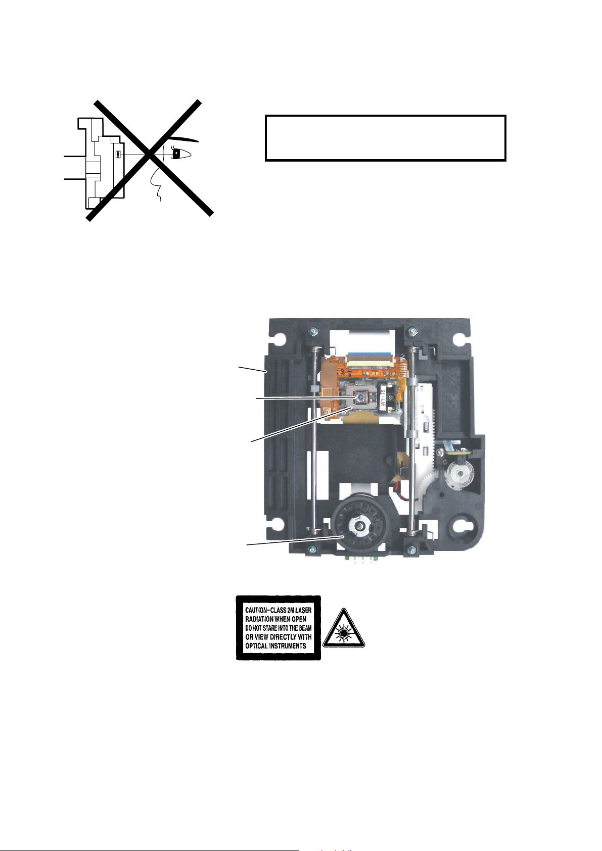
LASER BEAM SAFETY PRECAUTIONS
This DVD player uses a pickup that emits a laser beam.
Do not look directly at the laser beam coming
from the pic kup or allo w it to strike a gainst your
skin.
The laser beam is emitted from the location shown in the figure. When checking the laser diode, be sure to keep
your eyes at least 30 cm away from the pickup lens when the diode is turned on. Do not look directly at the laser
beam.
CAUTION: Use of controls and adjustments, or doing procedures other than those specified herein, may result in
hazardous radiation exposure.
Drive Mechanism Assembly
Laser Beam Radiation
Laser Pickup
Turntable
Location: Inside Top of DVD mechanism.
1-2-1 R3PLSP
Page 5

IMPORTANT SAFETY PRECAUTIONS
Product Safety Notice
Some electrical and mechanical parts have special
safety-related characteristic s which are often not evident from visual inspection, nor can the protection
they give necessarily be obtained by replacing them
with components rated for higher voltage, wattage,
etc. Parts that have special s afety characteristics are
identifi ed b y a ! on schematics and in parts lists. Use
of a substitute replacement that does not have the
same safety characteristics as the recommended
replacement part might create shock, fire, and/or other
hazards. The Product’s Safety is under review continuously and new instructions are issued whenever
appropriate. Prior to shipment from the factory, our
products are carefully inspected to confirm with the
recognized product safety and electr ical codes of the
countries in which they are to be sold. However, in
order to maintai n suc h c omp li anc e, it is e qual ly imp or tant to implement the following precautions when a set
is being serviced.
Precautions during Servicing
A. Parts identified by the ! symbol are critical for
safety. Replace only with part number specified.
B. In addition to safety, other parts and assemblies
are specified for conformance with regulations
applying to spur ious radi ation. Thes e must also be
replaced only with specified replacements.
Examples: RF conver ters, RF cables, noise blocking capacitors, and noise blocking filters, etc.
C. Use specified internal wiring. Note especially:
1)Wires covered with PVC tubing
2)Double insulated wires
3)High voltage leads
D. Use specified insulating materials for hazardous
live parts. Note especially:
1)Insulation tape
2)PVC tubing
3)Spacers
4)Insulators for transistors
E. When replacing AC primary side components
(transformers, power cord, etc.), wrap ends of
wires securely about the terminals before soldering.
F. Observe that the wires do no t co ntac t he at prod uc -
ing parts (heatsink s, oxide metal film resist ors, fusible resistors, etc.).
G. Check that replaced wires do not contact sharp
edges or pointed parts.
H. When a power cord has b een replac ed, check that
5 - 6 kg of force in any direction will not loosen it.
I. Also check areas surrounding repaired locations.
J. Be careful that foreign objects (screws, solder
droplets, etc.) do not remain inside the set.
K. Crimp type wire connector
The power transformer uses crimp type connectors
which connect the power cord and the primary side
of the transformer. When replacing the transformer,
follow these steps carefully and precisely to prevent shock hazards.
Replacement procedure
1)Remove the old connector by cutting the wires at a
point close to the connector.
Important: Do not re-use a connector. (Discard it.)
2)Strip about 15 mm of the insu lation from the ends
of the wires. If the wires are stranded, twist the
strands to avoid frayed conductors.
3)Align the lengths of the wires to be connected.
Insert the wires fully into the connector.
4)Use a crimping tool to crimp the metal sleeve at its
center. Be sure to crimp fully to the comp lete closure of the tool.
L. When connecting or disconnecting the internal
connectors, first, disconne ct the AC plug from the
AC outlet.
1-3-1 DVD_SFNP
Page 6
Safety Check after Servicing
Examine the area surrounding the repaired location
for damage or deterioration. Observe that screws,
parts, and wires have been returned to their original
positions. Afterwards, do the following tests and confirm the specified values to verify compliance with
safety standards.
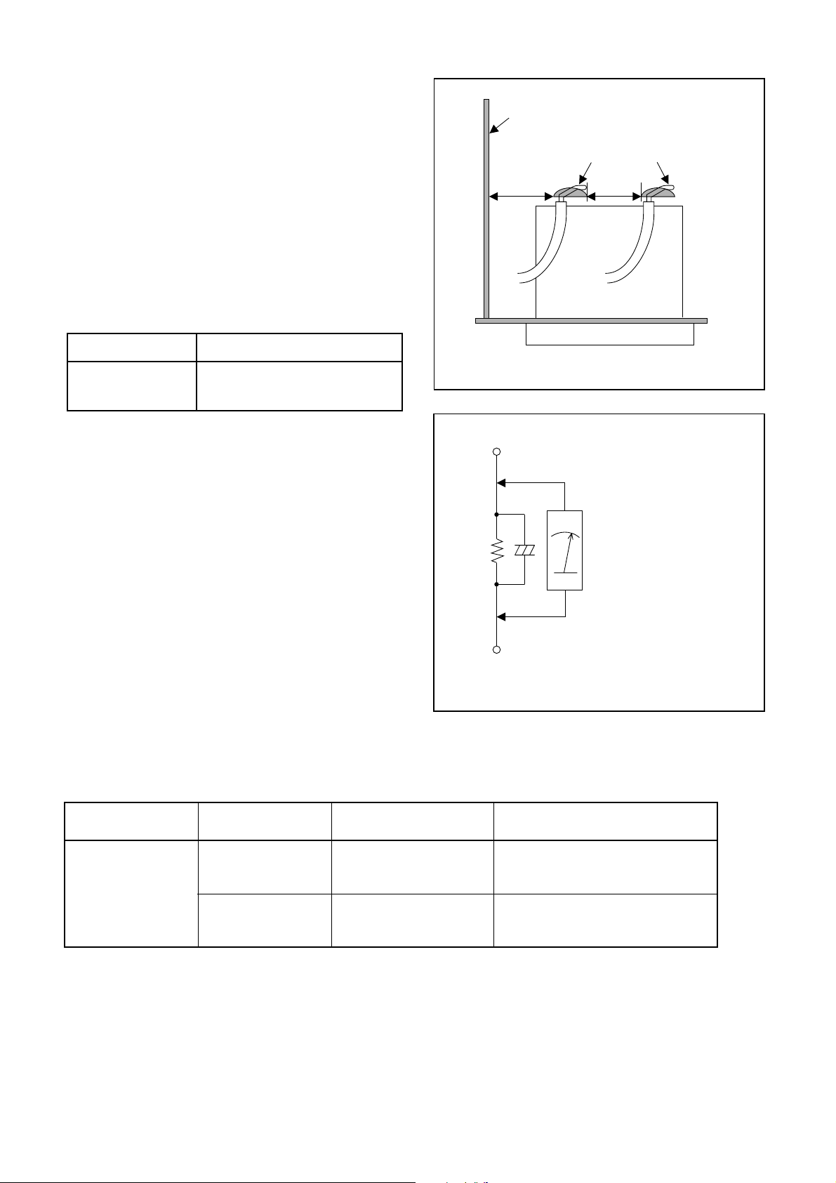
1. Clearance Distance
When replacing primary circuit components, confirm
specified clearance dista nce (d) and (d’) between soldered terminals, and between terminals and surrounding metallic parts. (See Fig. 1)
Table 1 : Ratings for selected area
AC Line Voltage Clearance Distance (d), (d’)
220 to 240 V
Note: This table is unofficial and for reference only.
Be sure to confirm the precise values.
2. Leakage Curre nt Test
≥ 3 mm(d)
≥ 6 mm(d’)
Chassis or Secondary Conductor
Primary Circuit
d' d
Fig. 1
Exposed Accessible Part
Confirm the specified (or lower) leakage current
between B (earth ground, power cord plug prongs)
and externally exposed accessible parts (RF terminals, antenna terminals, video and audio input and
output terminals, microphone jacks, earphone jacks,
etc.) is lower than or equal to the specified value in the
table below.
Measuring Method (Power ON) :
Insert load Z between B (earth ground, power cord
plug prongs) and exposed accessible parts. Use an
AC voltmeter to measure across t he ter minals of l oad
Z. See Fig. 2 and the following table.
Table 2: Leakage current ratings for selected areas
AC Line Voltage Load Z Leakage Current (i)
220 to 240 V
2kΩ RES.
Connected in
parallel
50kΩ RES.
Connected in
parallel
i≤0.7mA AC Peak
i≤2mA DC
i≤0.7mA AC Peak
i≤2mA DC
Z
One side of
B
Power Cord Plug Prongs
One side of power cord plug
AC Voltmeter
(High Impedance)
prongs (B) to:
RF or
Antenna terminals
A/V Input, Output
Fig. 2
Note: This table is unofficial and for reference only. Be sure to confirm the precise values.
1-3-2 DVD_SFNP
Page 7
STANDARD NOTES FOR SERVICING
Circuit Board Indications
1. The output pin of the 3 pin Regu lator ICs is indicated as shown.
Top View
Input
Out
2. F or other ICs, pin 1 and every fifth pin are indicated
as shown.
In
Pin 1
3. The 1st pin of every m ale con nec to r is ind icate d as
shown.
Bottom View
5
10
Pb (Lead) Free Solder
When soldering, be sure to use the Pb free solder.
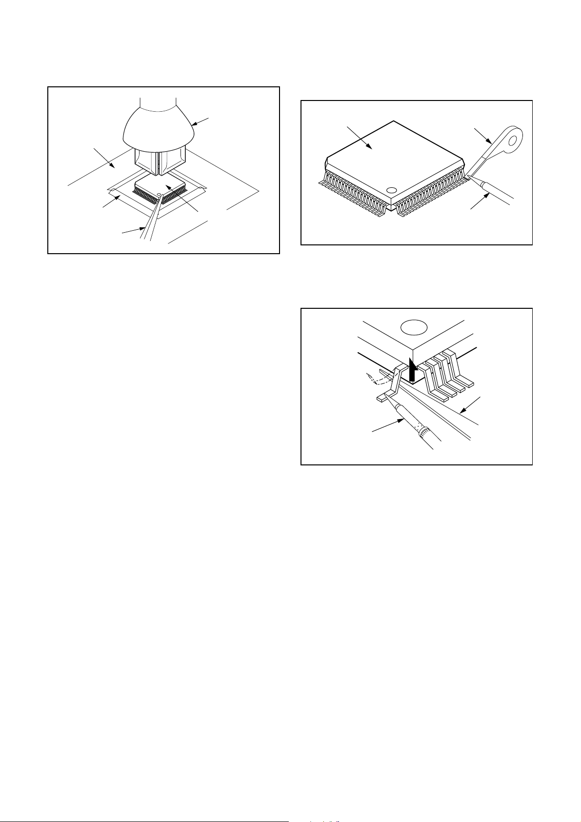
How to Remove / Install Flat Pack-IC
1. Removal
With Hot-Air Flat Pack-IC Desoldering Machine:.
(1)Prepare the hot-air flat pack-IC desoldering
machine, then apply hot air to the Flat Pack-IC
(about 5 to 6 seconds). (Fig. S-1-1)
Fig. S-1-1
Pin 1
Instructions for Connectors
1. When you connect or disconnect the FF C (Flexible
Foil Connector) cable, be sure to first disconnect
the AC cord.
2. FFC (Flexible Foil Connector) cable should be
inserted parallel into the connector, not at an angle.
FFC Cable
Connector
CBA
(2)Remove the flat pack-IC with tweezers while apply-
ing the hot air.
(3)B ottom of the flat pack-IC is fixed with glue to the
CBA; when removing entire flat pack-IC, first apply
soldering iron to c ent er of the fla t pack-IC and hea t
up. Then remove (glue will be melted). (Fig. S-1-6)
(4)Rel ease the flat pack-IC from the CBA using twee-
zers. (Fig. S-1-6)
Caution:
1. The Flat Pack-IC shape may differ by models. Use
an appropriate hot-air flat pack-IC desoldering
machine, whose shape matches that of the Flat
Pack-IC.
2. Do not supply hot air to the chi p parts aro und the
flat pack-IC for over 6 seconds because damage to
the chip parts may occur. Put masking tape around
the flat pack-IC to protect other parts from damage.
(Fig. S-1-2)
* Be careful to avoid a short circuit.
1-4-1 DVD_NOTE
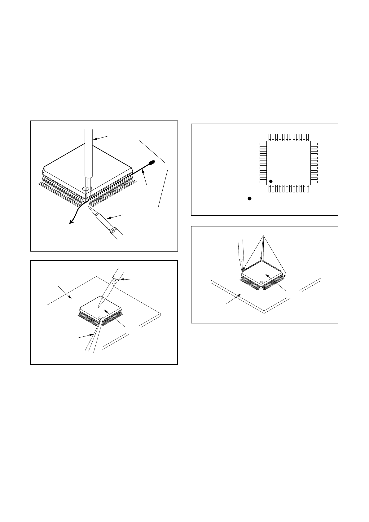
Page 8
3. The flat pack-IC on the CBA is affixed with glue, so
be careful not to break or dama ge the foil of each
pin or the solder lands under the IC when removing
it.
Hot-air
Flat Pack-IC
Desoldering
Machine
CBA
With Soldering Iron:
(1)Using desoldering braid, remove the solder from all
pins of the flat pack-IC. When you use sol der flux
which is applied to all pins of the flat pack-IC, you
can remove it easily . (Fig. S-1-3)
Flat Pack-IC
Desoldering Braid
Masking
Tape
Tweezers
Flat Pack-IC
Fig. S-1-2
Soldering Iron
Fig. S-1-3
(2) Lift each lead of the flat pack-IC upward one by
one, using a sharp pi n or wire to which solder will
not adhere (iron wire). W hen heating th e pins, use
a fine tip soldering iron or a hot air desoldering
machine. (Fig. S-1-4)
Sharp
Pin
Fine Tip
Soldering Iron
Fig. S-1-4
(3)B ottom of the flat pack-IC is fixed with glue to the
CBA; when removing entire flat pack-IC, first apply
soldering iron to c ent er of the fla t pack-IC and hea t
up. Then remove (glue will be melted). (Fig. S-1-6)
(4)Rel ease the flat pack-IC from the CBA using twee-
zers. (Fig. S-1-6)
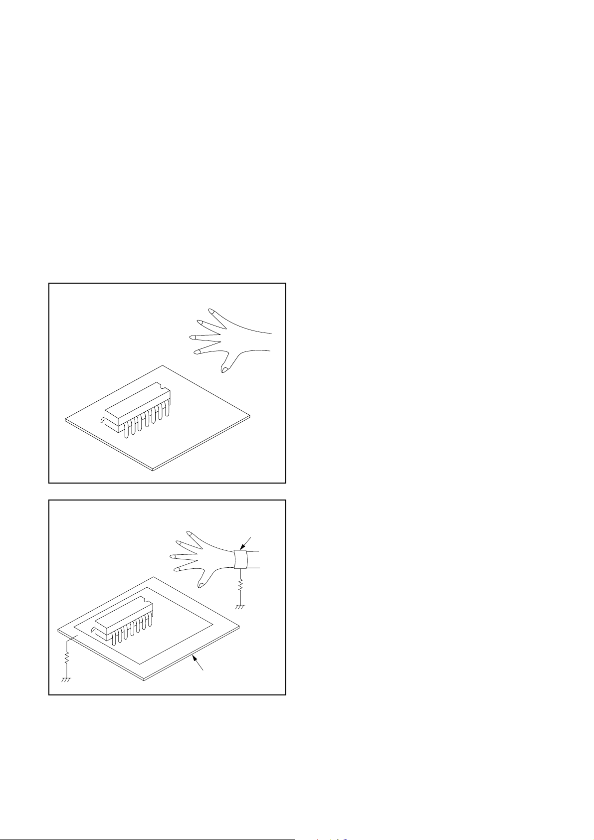
With Iron Wire:
(1)Using desoldering braid, remove the solder from all
pins of the flat pack-IC. When you use sol der flux
which is applied to all pins of the flat pack-IC, you
can remove it easily . (Fig. S-1-3)
(2) Affix the wire to a workbench or solid mounting
point, as shown in Fig. S-1-5.
(3) While heating the pins using a fine tip soldering
iron or hot air blower, pull up the wire as the solder
melts so as to l ift the IC leads from the CBA contact pads as shown in Fig. S-1-5.
1-4-2 DVD_NOTE
Page 9
(4)Bo ttom of the flat pack-IC is fixed with glue to the
CBA; when removing entire flat pack-IC, first apply
soldering iron to cente r o f the fl at p ack-IC and h eat
up. Then remove (glue will be melted). (Fig. S-1-6)
(5)Rel ease the fla t pack-IC from the C BA us ing twee -
zers. (Fig. S-1-6)
Note:
When using a solder ing iron, care must be taken
to ensure that the fl at pack-IC i s not bein g held by
glue. When the flat pack-IC is removed from the
CBA, handle it gentl y b ec ause i t m ay be dama ged
if force is applied.
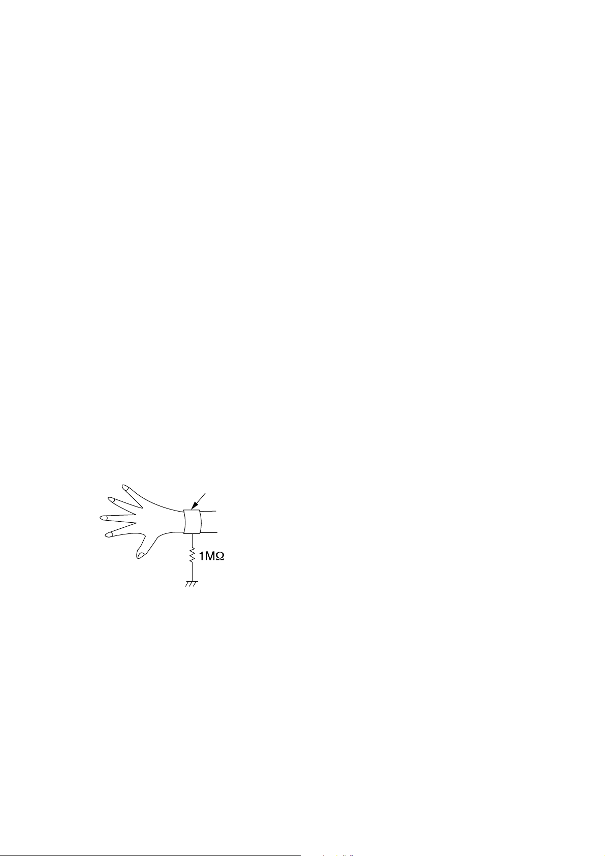
2. Installation
(1) Using desoldering braid, remove the solder from
the foil of each pin of the flat pack-IC on the CBA
so you can install a repla cement flat p ack-IC more
easily.
(2) The “I” mark on the flat pack-IC indicates pin 1.
(See Fig. S-1-7.) Be sure this mar k matches the 1
on the PCB when p ositioning for install ation. Then
presolder the four corn ers of the flat pack-IC. (See
Fig. S-1-8.)
(3)Solder all pins of the flat pack-IC. Be sure that none
of the pins have solder bridges.
To Solid
Mounting Point
CBA
Hot Air Blower
Iron Wire
Soldering Iron
Fig. S-1-5
Fine Tip
Soldering Iron
Example :
or
Pin 1 of the Flat Pack-IC
is indicated by a " " mark.
Fig. S-1-7
Presolder
Flat Pack-IC
CBA
Fig. S-1-8
Tweezers
Flat Pack-IC
Fig. S-1-6
1-4-3 DVD_NOTE
Page 10
Instructions for Handling
Semi-conductors
Electrostatic breakdown of the semi-conductors may
occur due to a potenti al difference caused by electrostatic charge during unpacking or repair work.
1. Ground for Human Body
Be sure to wear a groundi ng ban d (1M Ω) that is properly grounded to remove any static electr icity that may
be charged on the body.
2. Ground for Workbench
(1)Be sure to place a conductive sheet or copper plate
with proper grounding ( 1MΩ) on the wor kbench or
other surface, where the semi-conductors are to be
placed. Because the static electricity charge on
clothing will not escap e through the body grounding band, be care ful to avoid contacting semi-con ductors with your clothing.
< Incorrect >
< Correct >
1MΩ
CBA
Grounding Band
1MΩ
CBA
Conductive Sheet or
Copper Plate
1-4-4 DVD_NOTE
Page 11
HANDLING PRECAUTIONS FOR HDD
CAUTION:
1. SHOCK
a. Exposing HDD to shock may be the biggest
damaging factor. Please note that HDD is easily
damaged even if dropped from any height. Be sure
to place HDD on a shock-absorbent mat. Also, be
careful when transporting HDD.
b. Be careful not to subject HDD to any shock when
tightening screws for HDD replacement.
(Tighten screws manually, not with an electric
driver.)
2. MOISTURE
a. Moisture may also be a damaging factor. HDD is
semiclosed style. Sudden changes in ambient
temperature may cause moisture to form. Monitor
temperature and do not allow moisture to form on
the media surface. Also, when opening HDD
package, do so only after package is at ambient
temperature.
b. After replacing HDD, leave it to reach room
temperature (about 2 hours) for preventing dew
internal condensation, and then work necessary
task such as operation check.
4. OTHERS
a. Be careful so as not to do the followings.
Otherwise, HDD might be damaged.
- DO NOT disassemble HDD.
- When handling HDD, be sure to hold both sides
securely.
b. HDD should be stored, packed in the protective
bag, in suitable surroundings (i.e., no extreme
changes in temperature to avoid condensation).
c. When transporting HDD, be sure to use the
exclusive packing case (the replacement HDD
carton).
d. Do not stack HDDs.
e. Do not place vertically because HDD is unstable
and easy to fall.
3. STATIC ELECTRICITY
a. After removing HDD or taking replacement HDD
out of the protective bag (the replacement HDD is
packed in a protective bag), place HDD on a
conductive surface. A grounding band should be
worn when handling.
Grounding Band
Both the conductive surface and grounding band
should be grounded.
b. Make sure that HDD is placed on main unit
completely and then let go of it, when assembling.
c. Do not put HDD on a packing bag. (for preventing
electrostatic damage)
1-5-1 DHD_SN
Page 12
PREPARATION FOR SERVICING
How to Enter the Service Mode
About Optical Sensors
Caution:
An optical sensor system is used for the Tape Start
and End Sensors on this equipment. Carefully read
and follow the instructions below. Otherwise the unit
may operate erratically.
What to do for preparation
Insert a tape into the Deck Mechanism Asse mbly and
press [VCR PLAY] button. The tape will be loaded into
the Deck Mechanism Assembly. Make sure the power
is on, connect TP501 (S-INH) to GND. This will stop
the function of Tape Start Sensor, Tape End Sensor
and Reel Sensors. (If these TPs ar e c on nected before
plugging in the unit, the function of the sensors will
stay valid.) See Fig. 1.
Q503
TP501
S-INH
Note: Because the Tape End Sensors are inactive, do
not run a tape al l t he way to the start or the end of the
tape to avoid tape damage.
Q504
Fig. 1
1-6-1 E434APFS
Page 13
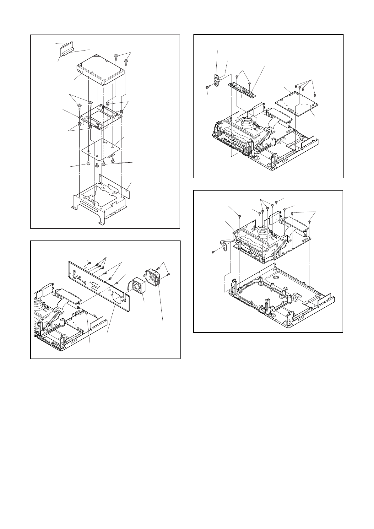
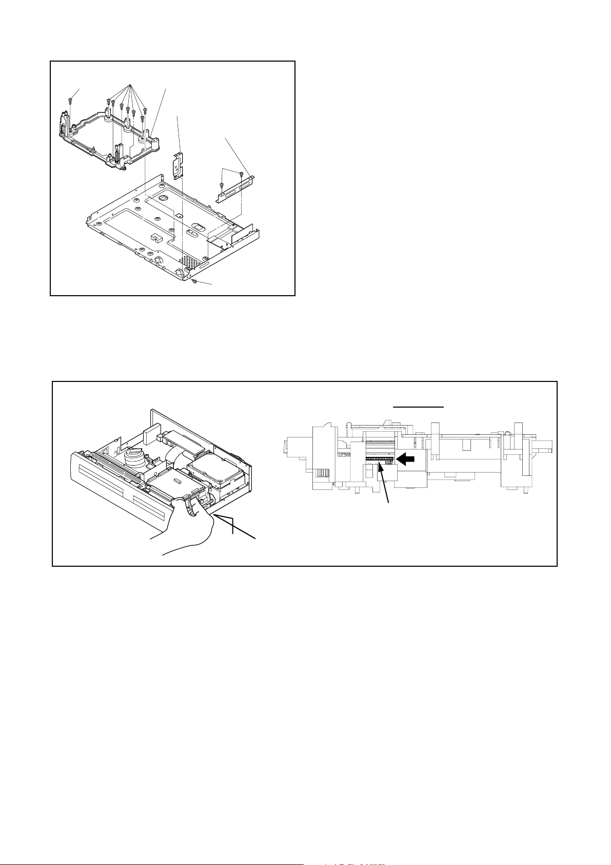
CABINET DISASSEMBLY INSTRUCTIONS
1. Disassembl y Flowchart
This flowchart indicates the disassembly steps to gain
access to item(s) t o be se rviced. Wh en re as se mbling,
follow the steps in reverse order. Bend, route, and
dress the cables as they were originally.
[1] T op Cover
[2] Front
Assembly
[21] Front
Bracket R
[22] Bracket R
[13] Power
Supply CBA
[14] SW CBA
[15] Front
Jack CBA
[3] Front
Bracket
[4] HDD
Assembly
[5] DVD
Mechanism &
DVD/HDD Main
CBA Assembly
[10] Fan
Holder
[11] Fan Motor
[6] HDD
Bracket
[7] HDD Unit
[8] HDD
Support
[9] ATA CBA
ID/
LOC.
No.
[6]
PART
HDD
Bracket
REMOVE/*UNHOOK/
Fig.
UNLOCK/RELEASE/
No.
UNPLUG/DESOLDER
Note
D4 4(S-7) ---
[7] HDD Unit D4 4(S-8), HDD Rubber
REMOVAL
HDD
[8]
Support
D4 Insulation Sheet ---
[9] ATA CBA D4 *CN3001, *CN3002 --[10] Fan Holder D5 2(S-9) --[11] Fan Motor D5 *CN1002 --[12] Rear Panel D5 5(S-10), 2(S-11) ---
Power
[13]
Supply
D6 *CL1001, 4(S-12) ---
CBA
[14] SW CBA D6 (S-13), Desolder ---
Front Jack
[15]
CBA
D6 *CN3001, 2(S-14) ---
2-1
2-2
2-3
[12] Rear
Panel
[16] VCR
Chassis Unit
[17] Deck
Assembly
[18] AV CBA,
AFV CBA
[20] Deck
Pedestal
[19] Power
SW CBA
2. Disassembl y Method
ID/
LOC.
No.
PART
Fig.
No.
[1] Top Cover D1 7(S-1) ---
Front
[2]
[3]
[4]
Assembly
Front
Bracket
HDD
Assembly
DVD
D2 (S-2), *5(L-1), *3(L-2)
D2
D3
Mechanism
[5]
&
DVD/ HDD
D3
Main CBA
Assembly
REMOVAL
REMOVE/*UNHOOK/
UNLOCK/RELEASE/
UNPLUG/DESOLDER
2(S-3), 3( S- 3B ), Front
Support
3(S-4), *CN201,
*CN1003
2(S-5), 2(S-6),
*CN1001, *CN1504,
Wiresheet
Note
1
1-1
1-2
1-3
---
---
2
[16]
[17]
[18]
[19]
[20]
[21]
VCR
Chassis Unit
Deck
Assembly
AV CBA,
AFV CBA
Power SW
CBA
Deck
Pedestal
Front
Bracket R
5(S-15), 4(S-16),
D7
(S-17)
(S-18), (S-19)
D8
Desolder
---
D8 ---------- ---
D8 Desolder ---
D9 8(S-20) ---
D9 (S-21) ---
[22] Bracket R D9 2(S-22) ---
↓
(1)
↓
(2)
↓
(3)
↓
(4)
(5)
Note:
(1):Identification (location) No. of parts in the figures
(2):Name of the part
(3):Figure Number for reference
(4):Identification of parts to be removed, unhooked,
unlocked, released, unplugged, unclamped, or
desoldered.
P=Spring, L=Locking Tab, S=Screw,
CN=Connector
*=Unhook, Unlock, Release, Unplug, or Desolder
e.g. 6(S-1) = six Screws (S-1),
5(L-1) = five Locking Tabs (L-1)
(5):Refer to “Reference Notes.”
3
4
↓
1-7-1 E434ADC
Page 14

Reference Notes
1. Locking T abs (L-1) and (L-2) are fragile. Be careful
not to break them.
1-1. Remove Screw (S-2).
1-2. Release five Locking Tabs (L-1).
1-3. Release three Locking Tabs (L-2) and
remove the Front Assembly.
2. Do not replace the DVD Mechanism or the DVD/
HDD Main CBA Assembly separately, when
replacing the DVD Mechanism & DVD/HDD Main
CBA Assembly. Order the new DVD Mechanism &
DVD/HDD Main CBA Assembly.
2-1. Whenever you have replaced the HDD unit,
initialize the HDD unit. To initialize the HDD
unit, perform the following.T o put the DVD/
VCR with HDD recorder into the HDD mode,
press the [HDD] button on the remote control
unit.
2-2. To put the DVD/VCR with HDD recorder into
the self-check mode, after pressing
[VARIABLE SKIP] button, press the [3], [6],
and [9] buttons on the remote control in that
order within three seconds.
2-3. Press [ENTER] button. The DVD/VCR with
HDD recorder is initialized and the power is
turned off automatically after two seconds.
3. When reassembling, solder wire jumpers as
shown in Fig. D8.
4. Before installing the Deck Assembly, be sure to
place the pin of LD-SW on the AV CBA as shown
in Fig. D8. Then, install the Deck Assembly while
aligning the hole of Cam Gear with the pin of LDSW, the shaft of Cam Gear with the hole of LD-SW
as shown in Fig. D8.
(S-3B)
(S-3B)
Front
Support
(S-3B)
(L-1)
(S-2)
(L-2)
[5] DVD Mechanism &
DVD/HDD Main CBA
Assembly
Wire
Sheet
(S-6)
CN201
(S-6)
[3] Front Bracket
(S-3)
(L-1)
[2] Front
Assembly
(L-1)
Fig. D2
[4] HDD Assembly
(S-4)
(S-4)
(S-5)
CN1504
CN1003
[1] T op Cover
(S-1)
(S-1)
(S-1)
(S-1)
(S-1)
Fig. D1
CN1001
Fig. D3
1-7-2 E434ADC
Page 15
CN3002
[9] ATA CBA
[7] HDD Unit
(S-7)
[8] HDD
Support
HDD Rubber
CN3001
(S-7)
HDD Rubber
Insulation Sheet
[14] SW CBA
(S-13)
Desolder
(S-14)
CN3001
[15] Front Jack CBA
(S-12)
CL1001
[13] Power
Supply CBA
(S-8)
(S-11)
(S-10)
[12] Rear Panel
CN1002
(S-8)
[6] HDD Bracket
Fig. D4
(S-10)
(S-11)
(S-9)
[11] Fan
Motor
[10] Fan Holder
Fig. D5
(S-15)
[16] VCR
Chassis
Unit
(S-17)
(S-15)
(S-16)
Fig. D6
(S-16)
(S-15)
(S-16)
Fig. D7
1-7-3 E434ADC
Page 16
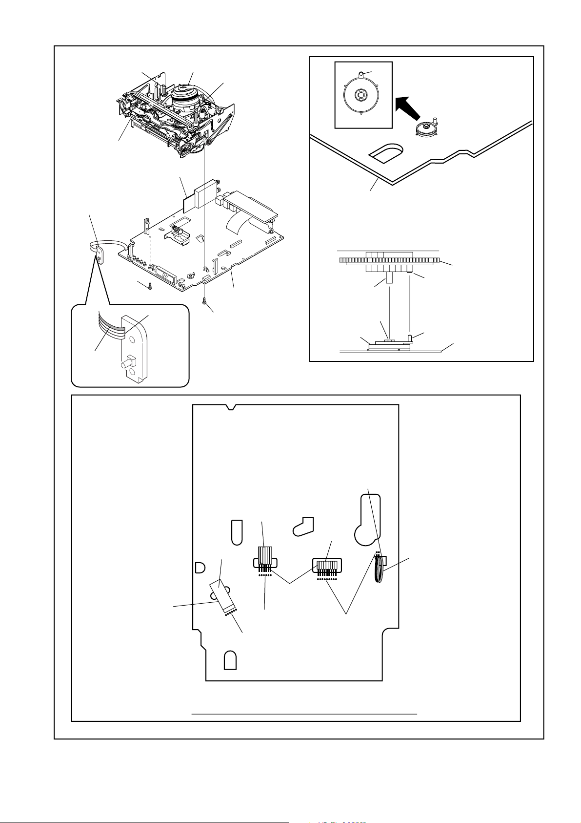
FE Head
[17] Deck
Assembly
Cylinder
Assembly
[18] AFV
CBA
ACE Head
Assembly
Pin
Pin
SW507
LD-SW
[19] Power
SW CBA
(S-18)
Lead with
blue stripe
Desolder
[18] AV CBA
(S-19)
From
ACE Head
Assembly
[18] AV CBA
[17] Deck Assembly
Shaft
Hole
LD-SW
From
FE Head
From
Cylinder
Assembly
Cam Gear
Hole
Pin
[18] AV CBA
From
Capstan
Motor
Assembly
Printing side
Lead with
blue stripe
Desolder
Desolder
Desolder
BOTT OM VIEW
Lead connections of Deck Assembly and AV CBA
1-7-4 E434ADC
Lead with
gray stripe
Fig. D8
Page 17
(S-20)
(S-20)
[20] Deck Pedestal
[21] Front Bracket R
[22] Bracket R
(S-22)
(S-21)
Fig. D9
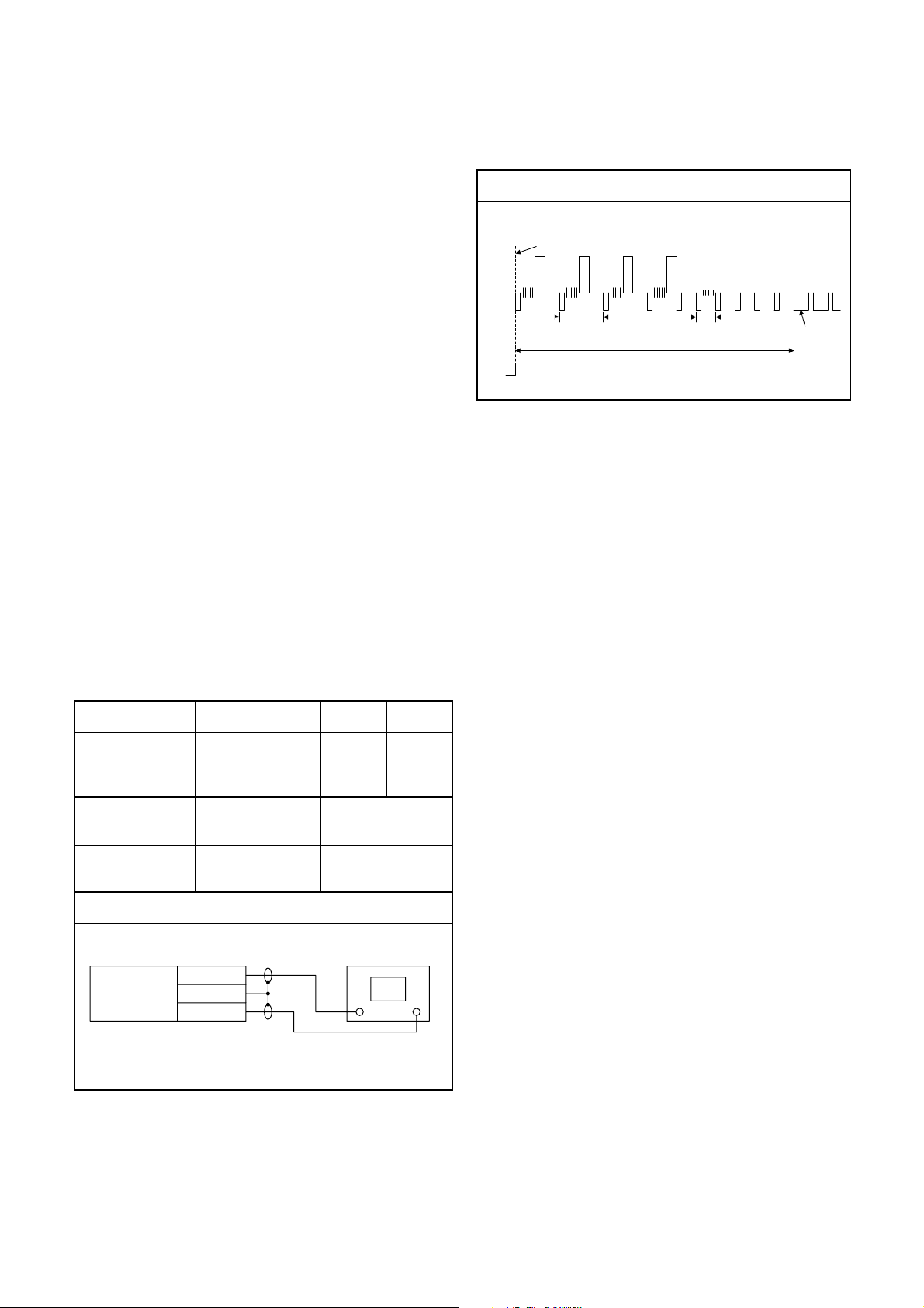
3. How to Eject Manually
Note: When rotating the gear, be careful not to damage the gear.
1. Remove the Top Cover.
2. Rotate the gear in the direction of the arrow manually as shown below.
Rotate this gear in
the direction of the arrow
A
View for A
1-7-5 E434ADC
Page 18
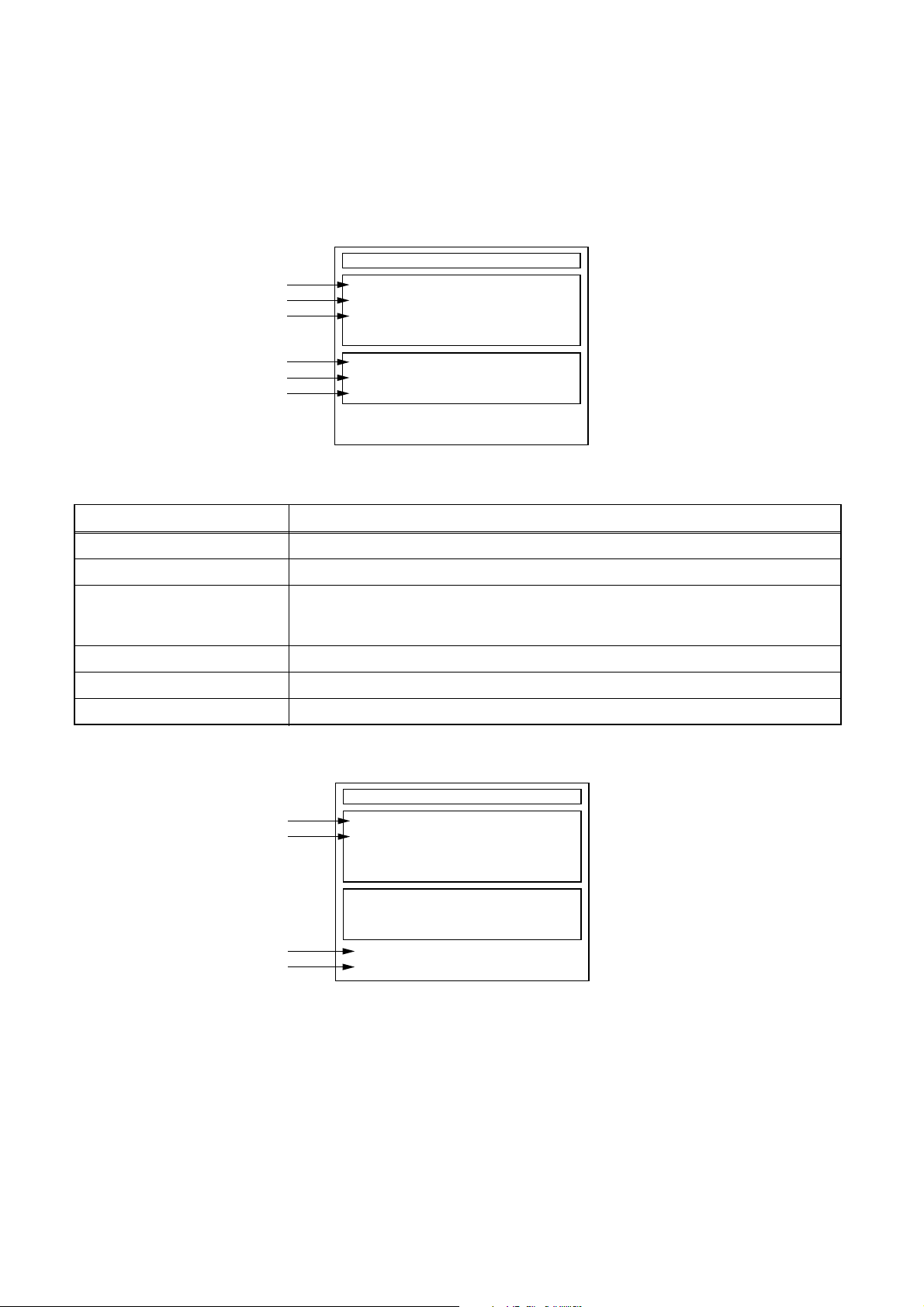
ELECTRICAL ADJUSTMENT INSTRUCTIONS
General Note: "CBA" is an abbreviation for
"Circuit Board Assembly."
NOTE:
1.Electri cal adjustm ents are re quired after re placing
circuit components and certain mechanical par ts.
It is impor tant to do these adjustments only after
all repairs and replacements have been completed. Also, do not attempt these adjustments
unless the proper equipment is available.
2.To perform these alignmen t / confir mation procedures, make sure that the tracking control is set in
the center position: Press either [PROG. L5??] or
[PROG. K] button on the front pan el fir st, then the
[VCR PLAY] button on the front panel.
Test Equipment Required
1.Oscilloscope: Dual-trace with 10:1 probe,
V-Range: 0.001~50V/Div.,
F-Range: DC~AC-20MHz
2.Alignment Tape (FL6A)
Head Switching Position Adjustment
Figure 1
EXT. Syncronize Trigger P oint
CH1
CH2
Reference Notes:
Playback the Alignment tape and adjust VR501 so that
the V-sync front edg e of the CH1 video out put waveform is at the 6.5H±1H (416µs±64µs) delayed position
from the rising edge o f the CH2 head switching pulse
waveform.
1.0H
6.5H±1H (416µs±64µs)
Switching Pulse
0.5H
V-Sync
Purpose:
To determine the Hea d Switching position during
playback.
Symptom of Misadjustment:
May cause Head Switching n oise or vertical jitter
in the picture.
Test point Adj.Point Mode Input
J340(JK2-V-OUT)
TP504(RF-SW)
GND
Tape
FL6A Oscilloscope
Connections of Measurement Equipment
Main CBA
TP504
VR501
(Switching Point)
(MAIN CBA)
Measurement
Equipment
J340
GND
PLAY
(SP)
Spec.
6.5H±1H
(416µs±64µs)
Oscilloscope
-----
CH1 CH2
Trig. (+)
1-8-1 E434AEA
Page 19
HOW TO SELF-CHECK AND INITIALIZE THE DVD/VCR WITH HDD
1. Turn on the DVD/VCR with HDD recorder.
2. To put the DVD/VCR with HDD recorder into the HDD mode, press [HDD] on the remote control unit.
3. To put the DVD/VCR with HDD recorder into the self-check mode, after pressing [VARIABLE SKIP] button,
press the [3], [6], and [9] buttons on the remote control in that order within three seconds.
Fig. a appears on the screen and all LEDs light.
"
" differs depending on the models.
*******
Self-Analysys and Report
*1
*2
*3
DVD CONNECT STATUS :
HDD CONNECT STATUS :
HDD POWER ON HOURS :
*4
*5
*6
BE Ver. :
FE Ver. :
Sub Micon Ver. :
T2*******Q2J
R20_0**_***h
NFQ2***T1-3N11
Fig. a: Self-Check Mode Screen
Table 1: Description of Fig. a
INDICATION DESCRIPTION
DVD CONNECT STATUS (*1) Connecting Condition of DVD(F/E)
HDD CONNECT STATUS (*2) Connecting Condition of HDD
Value of HDD power on hours obtained from S.M.A.R.T. command. (If not obtainable,
HDD POWER ON HOURS (*3)
value of HDD power on hours is “0”.)
Value in parentheses is the factory setting value. (If no setting, the value is “0”.)
BE Ver. (*4) B/E version
FE Ver. (*5) F/E version
Sub Micon Ver. (*6) Sub micro controller version
4. Upon the self-check completion, Fig. b appears on the screen.
"
" differs depending on the models.
*******
Self-Analysys and Report
*7
*8
DVD CONNECT STATUS : OK
HDD CONNECT STATUS : OK
HDD POWER ON HOURS : 100(40)
*10
BE Ver. :
FE Ver. :
Sub Micon Ver. :
*9
FACTORY DEFAULT :
POWER OFF :
T2*******Q2J
R20_0**_***h
NFQ2***T1-3N11
ENTER
POWER
Fig. b: Screen of Finishing Self-Check Mode
1-9-1 E434AINT
Page 20
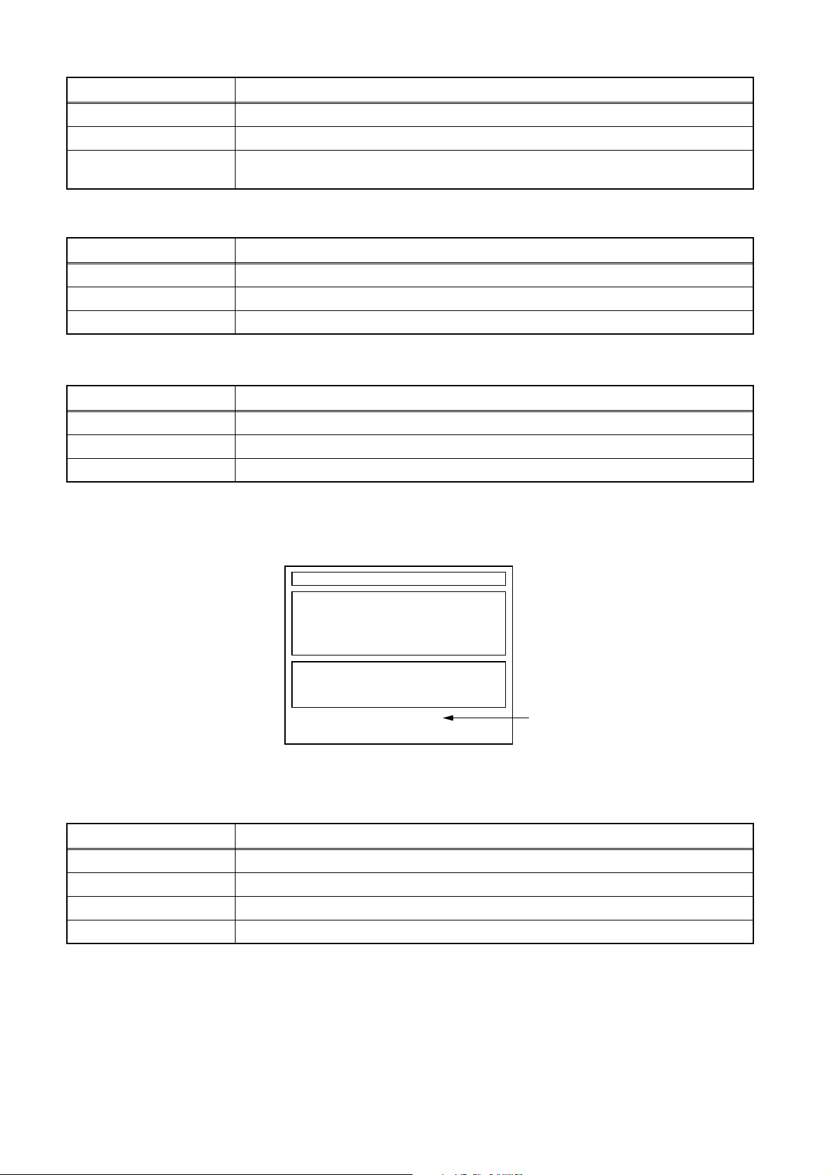
Table 2: Indication of DVD self-check (*7)
INDICATION DESCRIPTION
OK Connection of DVD is normal.
NOT FOUND DVD drive cannot be found.
CABLE ERROR
FFC cable (connecting to CN401) between the DVD drive and the DVD/HDD Main CBA is
not connected correctly.
Table 3: Indication of HDD self-check (*8)
INDICATION DESCRIPTION
OK Connection of HDD is normal.
NOT FOUND HDD drive cannot be found.
CABLE ERROR FFC cable between the ATA CBA and the HDD drive is not connected correctly.
Table 4: Availab le button in self-check mode
BUTTON DESCRIPTION
ENTER (*9) Initialize (only when the self-check mode is complete)
STANDBY-ON (*10) Turn the power off (when the self-check mode is complete)
OTHER Not available
5. When the self-check mode is complete, press [STANDBY-ON] button to turn the power off.
When initializing the DVD/VCR with HDD recorder, press [ENTER] button. Fig. c appears on the screen. After
two seconds, the power is turned off automatically.
"
" differs depending on the models.
*******
Self-Analysys and Report
DVD CONNECT STATUS : OK
HDD CONNECT STATUS : OK
HDD POWER ON HOURS : 100(40)
BE Ver. :
FE Ver. :
Sub Micon Ver. :
FACTORY DEFAULT : *11WRITING
T2*******Q2J
R20_0**_***h
NFQ2***T1-3N11
Fig. c: Initialize Mode Screen
Table 5: Description of *11 in Fig. c
INDICATION DESCRIPTION
ENTER Initialization preparation is complete.
WRITING Initializing
OK Initializing is finished normally.
NG Initializing is not finished normally.
NOTE: When initializing, “Current Clock”, “Setup Changing Item”, “Channel Setup”, “Area Setup”, “Program” and
“HDD Contents” are initialized.
1-9-2 E434AINT
Page 21
FIRMWARE RENEWAL MODE
1. Update Contents
Item Status
1 B/E Update B/E FIRMWARE
2 F/E Update F/E FIRMWARE
2. Update
1. Turn the power on and remove the disc in the tray.
2. To switch the DVD/VCR with HDD recorder into
the HDD mode, press [HDD] on the remote control
unit.
3. To put the DVD/VCR with HDD recorder into
version up mode, press [VARIABLE SKIP] and [6],
[5], [4] buttons on the remote control unit in that
order within 3 seconds. The tray will open
automatically.
Fig. a appears on the TV screen and Fig. b
appears on the VFD.
*FIRMWARE version will differ depending on the
model. Fig. a is an example.
DISC UPDATE
4. Load the update disc.
The TV screen will display Fig. c.
- If the update disc contains only a single file, the
update will initiate automatically when the disc is
inserted.
*FIRMWARE version will differ depending on the
model. Fig. c is an example.
DISC UPDATE
<DIR> BE
<DIR> FE
Fig. c: Update Disc TV Screen
Effective FIRMWA RE update files will have the file
extensions shown below.
File extension Status
BIN B/E FIRMWARE file
Please Insert F/W Disc
Fig. a: Update Mode TV Screen
Fig. b: VFD Display in Update Mode
MOT F/E FIRMWARE file
5. Select the desired FIRMWARE to be updated with
the arrow button and press the [ENTER] button.
FIRMWARE will automatically select the
appropriate F/E or B/E version.
Fig. d appears on the TV screen and Fig. e
appears on the VFD, and the update will start.
*FIRMWARE version will differ depending on the
model. Fig. d is an example.
DISC UPDATE
*1
TARGET: B/E
*2
STATUS: EXECUTING
DISC UPDATING xx% Complete
Fig. d: TV Display during update
The status displayed in *1 is as shown below.
Display Status
B/E FIRMWARE B/E
F/E FIRMWARE F/E
UNKNOWN Not FIRMWARE B/E or F/E
1-10-1 E434AFW
Page 22

The status di splayed in *2 is as shown below.
Display Status
EXECUTING
Loading F/W from Update Disc or
writing to Flash memory
OK Update successful
ERROR Error during Flash memory writing
FILE ERROR Check SAM error in F/W file
READ ERROR Error during F/W file reading
Fig. e: VFD Display during update
Re: the VFD display shown in Fig. e.
When the TV screen displays "Firmware
Updating... XX% Complete," the VFD will indicate
"XX"%.
6. When completing update, the tray will open
automatically.
The TV screen will display Fig. f.
*FIRMWARE version will differ depending on the
model. Fig. f is an example.
3. How to Verify the Firmware
Version
1. Turn the power on and remove the disc in the tray.
2. To switch the DVD/VCR with HDD recorder into
the HDD mode, press [HDD] on the remote control
unit.
3. Press [VARIABLE SKIP] and [1], [2], [3] buttons on
the remote control unit in that order within 3
seconds. The Firmware version appears on the TV
screen.
4. Press [STANDBY-ON] button to reset the unit.
DISC UPDATE
TARGET: B/E
STATUS: OK
DISC UPDATING 100% Complete
PLEASE PUSH POWER BUTTON
Fig. f: TV Display when completing update
If the update is completed correctly, the VFD will
indicate Fig. g.
Fig. g: VFD Display when completing update
Fig. h VFD Display when completing update with error
In this case, all button operations will be invalid
except [STANDBY-ON] button.
7. Press [STANDBY-ON] button to turn the power off
and press [STANDBY-ON] button again to turn the
power on and finish updating.
1-10-2 E434AFW
Page 23
FUNCTION INDICATOR SYMBOLS
< VCR Section >
Note:
If a mechanical malfunction occurs, the power is turned off. The following symbols will appear on the display.
Status Display
When reel or capstan mechanism is not
functioning correctly
When tape loading mechanism is not
functioning correctly
When cassette loading mechanism is not
functioning correctly
When the drum is not working properly
P-ON+5V Power safety detection
“W” blinks.
Fan does not rotate over 30 seconds.
When the power comes on again after that by pressing [S TANDBY-ON] button, an error message is disp layed on
the TV screen as follows.
When reel or capstan mechanism is not functioning
correctly
A
R
SP 0:00:00
When tape loading mechanism is not functioning
correctly
A
T
SP 0:00:00
“W” light and “R” blinks.
When the drum is not working properly
A
D
SP 0:00:00
Fig. 1
P-ON+5V Power safety detection
A
P
SP 0:00:00
Fig. 4
Fig. 2
When cassette loading mechanism is not functioning
correctly
A
C
SP 0:00:00
Fig. 3
Fig. 5
1-11-1 E434AFIS
Page 24
< DVD/HDD Section >
Note: If an error occurs, a message with the error number appears on the screen.
Recording Error
03-50
Error message
Error No.
Message Error No. Error Description Error Example
Disc error
Recording
error
System error
04-50
04-51
03-50
03-52 Loader error
03-53 Poor media
03-54
03-55 Writing error (video)
03-56 General error
03-57 Device error
03-60 Unrecorda ble disc
02-50
02-51 Disc protection failure
02-52 Format failure
02-53 Abnormal loader This code is outpu t w he n a n a ppro pria te DVD drive is no t c onn ec ted.
02-54
02-55
02-56
02-57 Fan lock
02-58 F/E hang-up
02-59 HDD hang-up
Renewal error at
ejecting disc
Disc includes still
picture
Recording error
caused by media
error
Control information
error and control data
error
Erasing error (all
titles)
Abnormal HDD
mount
Changing status
failure during VCR
dubbing
Abnormal VCR
mechanism
This code is output w h en t here is a c on t rol information writing failure
due to tray being open during writing or disc loading.
This code is output upon attempt to write data (fi nalizing disc protect
data, etc.) on a disc including a still picture.
This code is output when recording error caused by media error
occurs, e.g.,stopping recording during attempting to record on a
scratched disc.
This code is output when tray open/close error occurs. Also, when
the tray open error occurs at F/E and when the recovery fails even if
the B/E retries.
This code is output when a DVD operation error occurs during
copying.
This code is output when a chip (EMMA) outputs unusual data while
recording and the control information writing fails.
This code is output when video writing fails while copying at high
speed.
This code is output when a number of errors occur:
Ex.1) When Outplay list creation fails.
Ex.2) When the system can’t take the title information which should
be written on the disc.
Ex3) When starting to copy, recording is paused and restarted but,
after the recording pause, recording start fails.
This code is output when an HDD operation error occurs (HDD
recording error), while copying at high speed or constant speed.
This code is output when recording is attempted on a non recordable disc such as a CD or DVD-ROM.
This code is output when an error occurs er asi ng ent ire VR playlist,
HDD playlist or HDD originals.
This code is output when protected pre-existing information that
should be on a disc is missing (VR disc protection error).
This code is output when HDD formatting occurs in maintenance
mode.
This code is output when a [PLAY], [ST OP], [REC], [MENU] or [LIST ]
button is pressed while HDD is not functional.
This code is output when, during dubbing from HDD or DVD to VCR,
playback cannot be initiated or playback cannot be discontinued.
This code is output when a VCR mechanism abnormality occurs.
After the error message is displayed, the power turns off.
This code is output when fan locking (over 30 seconds) is detected.
After the error message is displayed, the power turns off.
This code is output when an F/E hang-up event occurs. After the
error message is displayed, the power turns off.
This code is output when HDD hang-up event occurs. After the error
message is displayed, the power turns off.
1-11-2 E434AFIS
Page 25
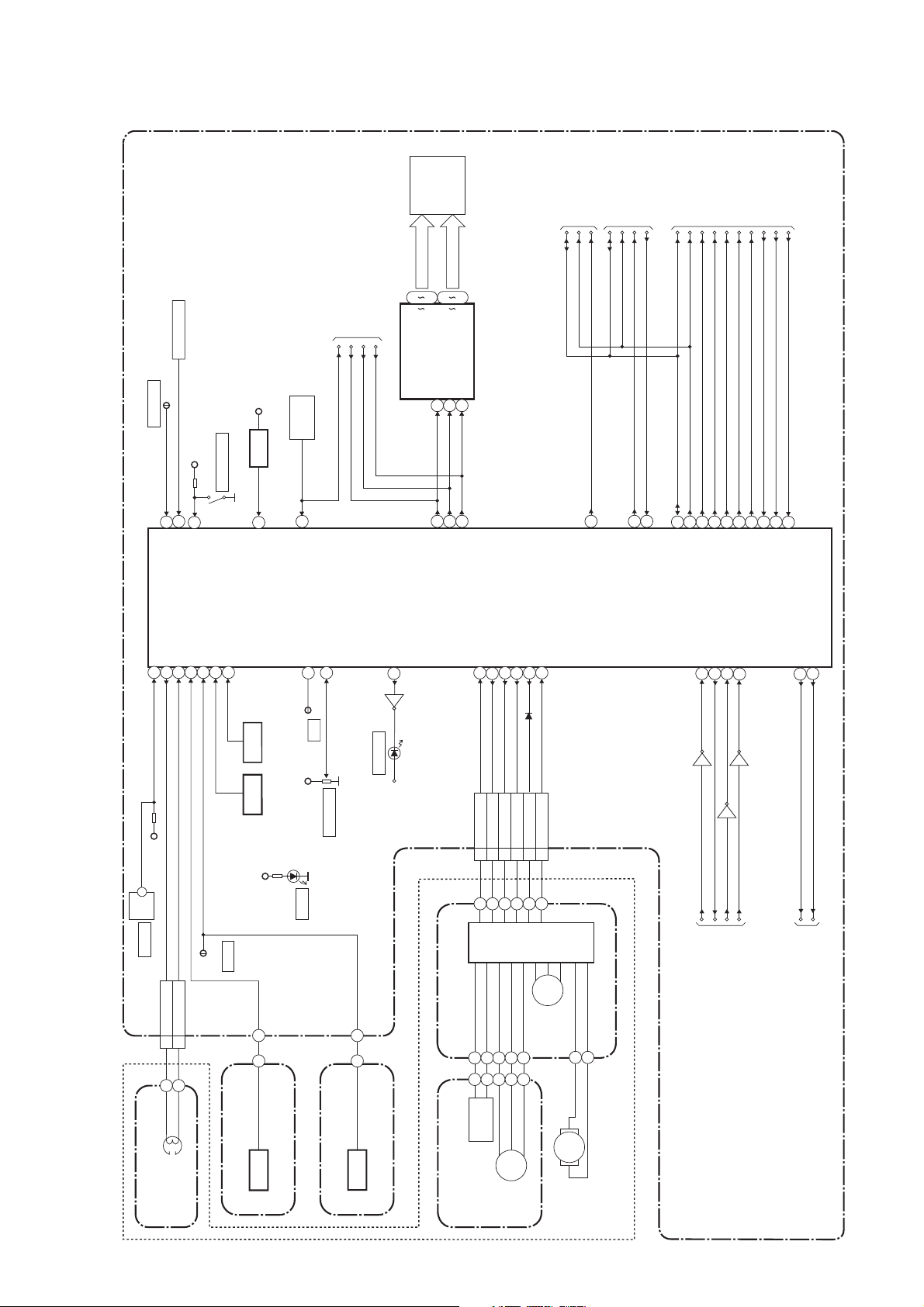
BLOCK DIAGRAMS
Servo/System Control Block Diagram
FIP
FL601
GRID
SEGMENT
7
23
17
a
1G
7G
(FIP DRIVER)
IC612
DIN
28
68
CLK
1
SENS-INH
TP501
KEY SWITCH
AL+5V
7
8
31
Q514,
REC-SAFETY
SW506
Q515
AL+5V
RESET
34
REMOTE
RM1501
14
SENSOR
TO SUB SYSTEM
CONTROL
BLOCK DIAGRAM
FL-DIN
FL-CLK
FL-STB
REMOTE
16
i
STB
2
69
TO AUDIO
BLOCK DIAGRAM
IIC-BUS SCL
IIC-BUS SDA
VCR-AUDIO-MUTE
83
TO Hi-Fi AUDIO
BLOCK DIAGRAM
A-MODE
Hi-Fi-H-SW
IIC-BUS SCL
IIC-BUS SDA
19
32
RF-SW
D-REC-H
IIC-BUS SCL
IIC-BUS SDA
33
71
72
TO VIDEO
BLOCK DIAGRAM
H-A-SW
C-ROTA
D-V-SYNC
16
13
15
18
V-ENV
C-SYNC
H-A-COMP
6
17
58
KEY- 1
KEY- 2
REC-SAF-SW
S-REEL79
ST-S
T-REEL
END-S
CTL(+)
CTL(-)
LD-SW9
IC501
(SERVO/SYSTEM CONTROL)
949510480
AL+5V
LD-SW
SW507
CN504
5 CTL(+)
6 CTL(-)
TP502
END-S
PS502
Q506
RESET
S-REEL
T-REEL
AL+5V
REMOCON-IN
CTL
97
CTL
TP503
AL+5V
VR501
D555
S-LED
PG-DELAY
2
SW-POINT
Q520
D520
VCR-REC
DRV-DATA
VCR-REC-LED
26
AL+5V
DRV-CLK70DRV-STB
C-CONT
LM-FWD/REV
C-FG
C-F/R
76
87
81
78
C-F/R5C-CONT7LM-FWD/REV
CN502
3 C-FG
4
MOTOR
DRIVE
CIRCUIT
CAPSTAN MOTOR
D-CONT77
D-PFG
90
D-CONT9D-PFG
8
M
CAPSTAN
MOTOR
A-MODE
Hi-Fi-H-SW
VCR-AUDIO-MUTE
RF-SW
D-REC-H
IIC-BUS SCL
IIC-BUS SDA
S-DATA-OUT
S-CS
65
64
Q516
S-DATA-OUT
S-CS
TO SUB SYSTEM
H-A-SW
C-ROTA
D-V-SYNC
H-A-COMP
S-DATA-IN
S-CLOCK
66
67
Q518
Q517
S-DATA-IN
S-CLOCK
CONTROL
BLOCK DIAGRAM
V-ENV
C-SYNC
C-POW-SW
TO SUB
75 P-ON-H
60 C-POW-SW
P-ON-H
POWER SUPPLY
BLOCK DIAGRAM
CONTROL
HEAD
ACE HEAD ASSEMBLY AV CBA
(DECK ASSEMBLY)
Q504
SENSOR CBA
ST-S
Q503
SENSOR CBA
END-S
PG
SENSOR
M
CYLINDER ASSEMBLY
DRUM
MOTOR
1-12-1
M
LOADING
MOTOR
E434GBLS
Page 26
Sub System Control Block Diagram
HDD-REC
DVD-REC
D3002
D3001
FRONT JACK CBA
EV+3.3V
Q1527
TIMER+5V
Q1528
TO SERVO/
SYSTEM CONTROL
BLOCK DIAGRAM
VCR
D3005
CN3001
CN1503
DVD
D3003
874
VCR-LED
DVR-REC-LED
HDD-REC-LED
874
HDD
D3004
6
5
DVD-LED
HDD-LED
6
5
RESET
SW3001
11
RESET
11
TO VIDEO SELECTOR
BLOCK DIAGRAM
SCL
SDA
TO SERVO/
SYSTEM CONTROL
BLOCK DIAGRAM
TO AUDIO SELECTOR
BLOCK DIAGRAM
AUDIO-MUTE
SCART-AUDIO-MUTE
DVD/HDD-AUDIO-MUTE
SCL
SDA
TU1501(TUNER UNIT)
SCL
9
SDA
10
IC1504
(SUB MICRO CONTROLLER)
RESET
IC1502
1 2
14
RESET
PW-SW
REG-CONT
23
52
LOW-POW
32
30
P-DOWN
FAN-LOCK
FAN-CONT1
3
53
C1547
(BACKUP CAPACITOR)
7
BUP+3.3V
FL-DIN
FL-CLK
485049
FL-DIN
FL-STB
FL-CLK
FL-STB
OSC2
8
8MHz
X1502
REMOTE
27
REMOTE
OSC1
9
RESONATOR
X OUT
12
32.768KHz
X1501
X IN
11
X'TAL
55
DVD-REC-LED
SUB-RXD
SYS-RESET
221918
CN1504
30SYS-RESET
29SUB-RXD
302927
CN601
56
57
58
59
DVD-LED
VCR-LED
HDD-LED
HDD-REC-LED
SUB-TXD
REG-CONT2
26
27SUB-TXD
26
REG-CONT2
26
S-DATA-IN
S-DATA-OUT
15
VCR-TXD
S-CS
S-CLOCK
16
17
24
VCR-CS
VCR-CLK
VCR-RXD
POWER-LED
60
CN1505
1
POWER-LED
1
CN1601
40
DVD/HDD-A-MUTE
2
POWER-SW
2
Q1530
38
393334
I2C-SDA
AUDIO-MUTE
SCART-AUDIO-MUTE
Q1529
I2C-SCL
KEY-1
KEY-2
1
2
KEY SWITCH
CN1503
1
10
KEY-1
KEY-2
1
10
CN3001
AV CBA
DUBBING-LED
31
2
DUBBING-LED
2
REG-CONT
LOW-POW
PWR -SW
TO SUB
POWER SUPPLY
FAN-LOCK
FAN-CONT1
BLOCK DIAGRAM
24.576MHz
X801
X'TAL
R20
CLK 24 IN
A2
P20
CLK 24 OUT
SYS-RESET
N20
M20
SUB-TXD
SUB-RXD
EV+2.4VP-ON+1.5V
+1.5V
IC501
D1601
REGULATOR
DVD/HDD MAIN CBA
IC601
(MAIN MICRO CONTROLLER)
1-12-2
SW1601
POWER
KEY SWITCH
POWER
OPEN/CLOSE
SW3009
POWER SW CBA
KEY SWITCH
FRONT JACK CBASW CBA
CN3002
3
114
KEY-1
KEY-2
DUBBING-LED
3
4
CN3003
DUBBING
D3006
E434GBLSS
Page 27

Digital Signal Process Block Diagram
TO VIDEO
SELECTOR
BLOCK
DIAGRAM
VIDEO-C-IN
VIDEO-Y/CVBS-IN
VIDEO-Y(I/P)-OUT
7
21
23
CN601
J18
H18
D/A
D/A
(CN1504)
VIDEO-Cr/Pr-OUT
VIDEO-Cb/Pr-OUT
VIDEO-Y(I)-OUT
VIDEO-C-OUT
519
3
K18
H19
D/A
D/A
VIDEO
ENCODER
G19
D/A
V15
W17
VIDEO
DECODER
IC901
(AUDIO D/A CONVERTER)
CN601
768
T20
N19
TO AUDIO
SELECTOR
BLOCK
AUDIO(L)-OUT
AUDIO(R)-OUT
DVD/HDD-AUDIO-MUTE
17
15
19
151416
L-CH
R-CH
MUTE
AUDIO
D/A
CONVER
-TER
4
V4W4V3
M19
DIAGRAM
AUDIO(L)-IN
13
3
(CN1504)
AUDIO(R)-IN
11
5
2
U20
IC902
P19
(AUDIO A/D CONVERTER)
1
R-CH
L-CH
101112
H20
2
AUDIO
A/D
G20
CONVER
-TER
F20
DIGITAL
AUDIO OUT
FIBER OPTIC
TRANS MODULE
DIGITAL
AUDIO OUT
(OPTICAL)
JK1501
(REAR)
(COAXIAL)
JK1502(REAR)
AV CBA
BUFFER
Q1533
CN1501
30 30SPDIF
CL1001
CN1001
15
11SPDIF
CN501
E20
WF10
POWER
SUPPLY CBA
REC VIDEO SIGNAL PB VIDEO SIGNAL REC AUDIO SIGNAL PB AUDIO SIGNAL
IC601 (MPEG2 AV CODEC)IC201
IC101
CN201CN3001
RF/
ERROR AMP
VIDEO
IC102
CN101
AUDIO
CN401
I/F
IC202
+3.3V
FLASH
MEMORY
IC401
MOTOR
DRIVER
FLASH MEMORY
IC604,IC605 (FLASH MEMORY)
DDR SDRAM
IC602,IC603 (DDR SDRAM)
SDRAM
IC204
DVD/HDD MAIN CBA
I/F
BACK-END
DIGITAL
SIGNAL
PROCESS
FRONT-END
DIGITAL
SIGNAL
PROCESS
LPC
IC402
MOTOR
DRIVER
IC410
OP AMP
CN3002
HARD
DISK
DRIVE
ATA CBA
DVD MECHANISM
TILT
PICK
TRACKING
-UP
FOCUS
CN1003
ENCODER
CBA
1-12-3
FE
ENCODER
CN1001
TRAY OPEN
LOADER
CBA
SLED
MOTOR
M
CN1002
SPINDLE
MOTOR
RELAY
CBA
M
E434GBLD
Page 28
Video Selector Block Diagram
AV CBA
REC VIDEO SIGNAL PB VIDEO SIGNAL
VIDEO
JK2001
20
10
VIDEO-IN2
10
CN1507 CN2001
121614
GCL
LPF
IN2
SW
SW
S-VIDEO
IN1
IC3001
(FRONT)
C
21
3 4
Y
100
SW
FRONT JACK CBA
VIDEO OUT
TU1501
(TUNER UNIT)
17
7
9
SW
AGC
SW
LPF
TO SUB SYSTEM
CONTROL
BLOCK DIAGRAM
SCL
SDA
42
43
I/F
IIC
SW
VIDEO
-IN1
JK3001
(FRONT)
REAR JACK
CBA
12
16
VIDEO IN1
JK1504
20
20
65
64
SW
SW
CN1503 CN3001
AGC
S-VIDEO-C-IN-F
VIDEO-IN1
S-VIDEO-Y-IN-F
S-VIDEO-Y-IN-F
141412
16
SW
(VIDEO SELECTOR)IC1506
REAR JACK
CBA
Q2001
JK2001
SW
DRIVER FBC
224850
8
13
VIDEO-OUT2
VIDEO-G-IN
8
13
CN2001 CN1507
BUFFER
19
11
49
12
14
VIDEO-B-IN
VIDEO-R-IN
12
14
7
15
MUTE
61
BUFFER
Q1514
MUTE
59
BUFFER
Q1512
SW
5152535557
WF4
WF8
VIDEO-Y/CVBS-IN
VIDEO-Y(I/P)-OUT
CN1504
7
21
23 VIDEO-C-IN
+
WF7WF5
VIDEO-Cr/Pr-OUT
VIDEO-Cb/Pb-OUT
VIDEO-Y(I)-OUT
VIDEO-C-OUT
3
5
1
9
WF6
Q1601
JK1504
SW
MUTE FBC
DRIVER
30
BUFFER
19
11715
SW
DRIVER
46
SW
DRIVER
44
SW
DRIVER
45
SW
MUTE
DRIVER FBC
36
MUTE
DRIVER
34
CY
4
3
JK1505
SW
21
(REAR)
S-VIDEO
+
OUT
SW
24
VCR-VIDEO-IN
VCR-VIDEO-OUT
TO VIDEO
BLOCK
DIAGRAM
VIDEO-B
VIDEO-R
VIDEO-G
VIDEO OUT2
TO DIGITAL
SIGNAL
PROCESS
BLOCK
DIAGRAM
(CN601)
1-12-4
VIDEO-B
VIDEO-R
VIDEO-G
VIDEO OUT1
E434GBLVS
Page 29

Video Block Diagram
VIDEO (L)-1
HEAD
VIDEO (R)-1
HEAD
VIDEO (L)-2
HEAD
CYLINDER ASSEMBLY
VIDEO (R)-2
HEAD
MODE: SP/RECPB-VIDEO SIGNAL
REC-VIDEO SIGNAL
TO SERVO/SYSTEM
IIC-BUS SCL
CONTROL BLOCK
DIAGRAM
IIC-BUS SDA
(DECK ASSEMBLY)
CN251
7978
Y. DELAY
46 43
6968
SERIAL
DECORDER
65
123
VIDEO(L)-1
VIDEO(R)-1
VIDEO-COM
969594
SP
HEAD
SP
P
R
LUMINANCE
SIGNAL
PROCESS
AGC
456
VIDEO(L)-2
VIDEO(R)-2
VIDEO-COM
93
AMP
EP
WF2
RF-SW
TP504
908988
EP
HEAD
AMP
REC FMAGC
Y
CCD 1H DELAY
CHARA.
INS.
87
+
1/2
RF-SW
D-REC-H
80
D-REC-H
C
FBC
C-ROTA
70
RF-SW/C-ROTA
CHROMINANCE
TO SERVO/SYSTEM
CONTROL BLOCK
DIAGRAM
V-ENV
H-A-SW
H-A-COMP
83
71
62
H-A-SW
D-V-SYNC
H-A-COMP
RPRP
PROCESS
C-SYNC
67
84
V-ENV
C-SYNC
Y/C
PR
MIX
AGC
D-V-SYNC
SIGNAL
VXO
21
2928
C-PB
TP301
X301
WF3
4.43MHz
AV CBA
IC501 (OSD)
50
OSD
CHARACTER
MIX
52
VIDEO SIGNAL PROCESS
/HEAD AMP
IC301
BUFFER
Q402
BYPASS
48
VCR-VIDEO-OUT
VCR-VIDEO-IN
TO VIDEO
SELECTOR
PB/EE
MUTE
56
WF1
BLOCK DIAGRAM
1-12-5
58 59
61
E434GBLV
Page 30

Audio Selector Block Diagram
IF SINAL
AUDIO(R)-IN2
AUDIO(L)-OUT2
AUDIO(R)-OUT2
AUDIO(L)-IN2
2
613
JK2001
MUTE-ON
Q2002
REAR JACK CBA
CN2001
AUDIO(L)-IN2
66
CN1507
MUTE-ON
Q2003
2
AUDIO-MUTE
AUDIO(R)-IN2
AUDIO(L)-OUT2
AUDIO(R)-OUT2
2
55
11
33
72
AUDIO(L)-IN1
613
JK1504
TP1522
A-OUT(L)
71
AUDIO(R)-IN1
AUDIO(L)-OUT1
AUDIO(R)-OUT1
2
Q1538
Q1537
AFV CBA
MUTE-ON
MUTE-ON
TP1521
74
PROCESS
CN1
SIF
TU-AUDIO(L)
22
55
CN1508
Q1534
DRIVE
A-OUT(R)
73
AUDIO(L)
-OUT
(REAR)
JK1503
TU-AUDIO(R)
44
SIF OUT
TU1501 (TUNER UNIT)
7
67
68
Q1539
MUTE-ON
AUDIO(R)
-OUT
Q1540
MUTE-ON
90
Q1536
948592
(FRONT)
JK3002
CN3001
18
AUDIO(L)-IN-F
18
CN1503
DRIVE
82
AUDIO(L)
-IN1
(FRONT)
JK3003
AUDIO(R)-IN-F
20 20
AUDIO(R)
-IN1
8993849181
TO Hi-Fi AUDIO
FRONT JACK CBA
BLOCK DIAGRAM
VCR-AUDIO-IN(L)
VCR-AUDIO-IN(R)
TO SUB
SYSTEM CONTROL
BLOCK DIAGRAM
AUDIO-MUTE
SCART-AUDIO-MUTE
DVD/HDD-AUDIO-MUTE
REC AUDIO SIGNAL PB AUDIO SIGNAL
I/F
IIC
IC1506(AUDIO SELECTOR)
42
43
SDA
SCL
SW
(OP AMP)
IC1505
OP
77
1
2
SW
AMP
OP
76
7
6
AMP
SW
SW
SW
SW
SW
SW
)
OP AMP
(
IC1501
(DVD/HDD VCR DUBBING)
(VCR DVD/HDD DUBBING)
SW
80
2
OP
AMP
1
70
SW
OP
79
6
7
SW
AMP
SW
69
VCR-AUDIO-OUT(L)
VCR-AUDIO-OUT(R)
AV CBA
TO SUB SYSTEM
TO Hi-Fi
AUDIO
BLOCK
WF9
CONTROL
BLOCK DIAGRAM
AUDIO(L)-OUT
AUDIO(R)-OUT
DVD-AUDIO-MUTE
17
15
TO DIGITAL
SIGNAL
AUDIO(L)-IN11AUDIO(R)-IN
19
13
PROCESS
BLOCK
DIAGRAM
(CN601)
CN1504
1-12-6
DIAGRAM
E434GBLAS
Page 31

Audio Block Diagram
Mode : SP/REC
ALC
12
DET
11
MUTE
LINE
ALC
AMP
REC-ON
SERIAL
DECODER
TO SERVO/SYSTEM
CONTROL BLOCK
DIAGRAM
IIC-BUS SCL
IIC-BUS SDA
VCR-AUDIO-MUTE
71
68 69
PB-AUDIO SIGNAL REC-AUDIO SIGNAL
AV CBA
13
IC301
(AUDIO SIGNAL PROCESS)
INV
PB-ON
P
R
ATT
98
7
EQ
AMP
SP/LP-ON
5
6
+5V
Q404
Q403
BIAS
OSC
REC
AUTO
1
AMP
100
3
BIAS
2
Q406
16
AUDIO HD-SW
CONTROL
SWITCHING
D-REC-OFF
Q405
+5V
Q401
(PB=ON)
N-A-PB
N-A-REC
TO Hi-Fi AUDIO
BLOCK DIGRAM
1-12-7
CN504
ACE HEAD ASSEMBLY
(DECK ASSEMBLY)
AUDIO-PB/REC
4
3 A-COM
1 AE-H
2 AE-H/FE-H
AUDI O
HEAD
AUDI O
ERASE
HEAD
CN501
2 FE-H
FE HEAD
FULL
ERASE
1 FE-H-GND
HEAD
E434GBLA
Page 32

Hi-Fi Audio Selector Block Diagram
TO AUDIO
SELECTOR
BLOCK DIAGRAM
TO
SERVO/ SYSTEM
CONTROL BLOCK
DIAGRAM
Hi-Fi
AUDIO(R)
HEAD
Hi-Fi
AUDIO(L)
HEAD
CYLINDER ASSEMBLY
REC-AUDIO SIGNALPB-AUDIO SIGNAL Mode : SP/REC
VCR-AUDIO-IN(L)
VCR-AUDIO-IN(R)
IIC-BUS SCL
IIC-BUS SDA
37
38
SERIAL
DATA
DECODER
R-CH
BPF
COMP
SW
NOISE
P
A-MODE
Hi-Fi-H-SW
767774
MUTE-ON
LPF
VCO
LIM DEV
R
OUTPUT
MUTE-ON
SELECT
73
39
HOLD
(DECK ASSEMBLY)
75
26
COMP
MIX
PULSE
NOISE
DET
Q451
21
ENV
LPF
VCO
LIM DEV
DET
R
DO
7
CN251
AUDIO(R)
Hi-Fi-
24
R
DET
P
Hi-Fi-COM 8
34 33
LIM
L-CH
COMP
SW
9
AUDIO(L)
Hi-Fi-
27
L
BPF
NOISE
AV CBA
IC451 ( Hi-Fi AUDIO PROCESS)
R-CH
PNR
47
48
R-CH
INSEL
50
VCR-AUDIO-OUT(R)
VCR-AUDIO-OUT(L)
TO AUDIO
SELECTOR
BLOCK DIAGRAM
14
L-CH
4
15
INSEL
L-CH
PNR
NOR
SW
78
80
N-A-REC
N-A-PB
TO AUDIO
BLOCK DIAGRAM
1-12-8
E434GBLH
Page 33

Power Supply Block Diagram
TO
POWER SUPPLY
BLOCK DIAGRAM
(CN1501)
AL+5V(3)
1 AL-30V
2 AL+44V
CL1001
CAUTION !
Fixed voltage (or Auto voltage selectable) power supply circuit is used in this unit.
If Main Fuse (F1001) is blown , check to see that all components in the power supply
circuit are not defective before you connect the AC plug to the AC power supply.
Otherwise it may cause some components in the power supply circuit to fail.
14 P-ON+9V(1)
7,8 AL+12V
3,4 AL+16.3V
Q1106
P-ON+5V(A)
22 AL+5V
15,16
17,18
SW+5V
23 F1
24 F2
25 REG-CONT
26 LOW-POW
SW+5V
Q1108-Q1111
12 FAN-CONT1
27 PWR-SW
13 FAN-LOCK
Q1105
+9V REG.
FAN
1FAN
CN1002
Q1114
2 FAN-LOCK
Q1115
HARD
4 HDD+12V
CN1003
DISC
DRIVE
1 HDD+5V
4-6 EV+10.5V
CN1001
TO
DVD/HDD
MAIN CBA
EV+2.4V
P-ON+5V
14-17
11-13
(CN501)
P-ON+3.3V
P-ON+2.5V
25-27
20-22
+2.5V REG.
IC1103
+3.3V REG.
IC1104
Q1107
18
17
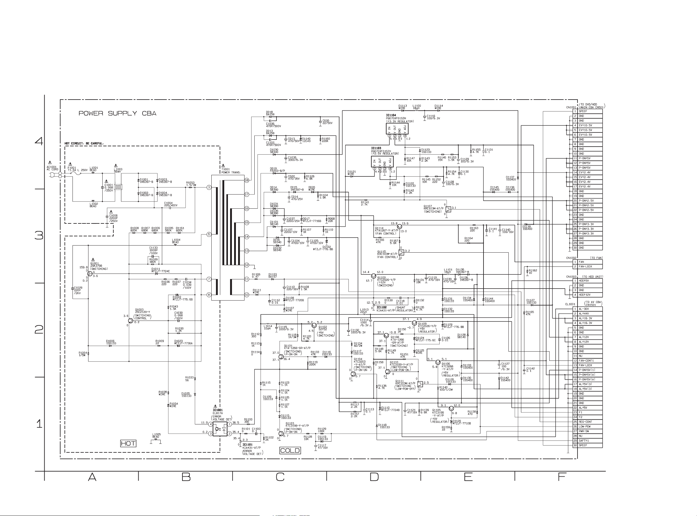
NOTE:
The voltage for parts in hot circuit is measured using
hot GND as a common terminal.
3
T1001
BRIDGE
RECTIFIER
D1001 - D1004
16
5
15
Q1001
14
SW+12V
Q1100
Q1003
Q1101
13
SW-CTL
IC1102
Q1104
12
11
10
7
8
Q1102
IC1001
ERROR
VOLTAGE DET
Q1103
1
3
2
REG.
1
4
2
3
SHUNT
IC1101
POWER SUPPLY CBA
HOT COLD
LINE
FILTER
L1003
CAUTION !
For continued protection against fire hazard,
replace only with the same type fuse.
HOT CIRCUIT. BE CAREFUL.
F1001
T1.6A L 250V
AC1001
1-12-9
E434GBLP
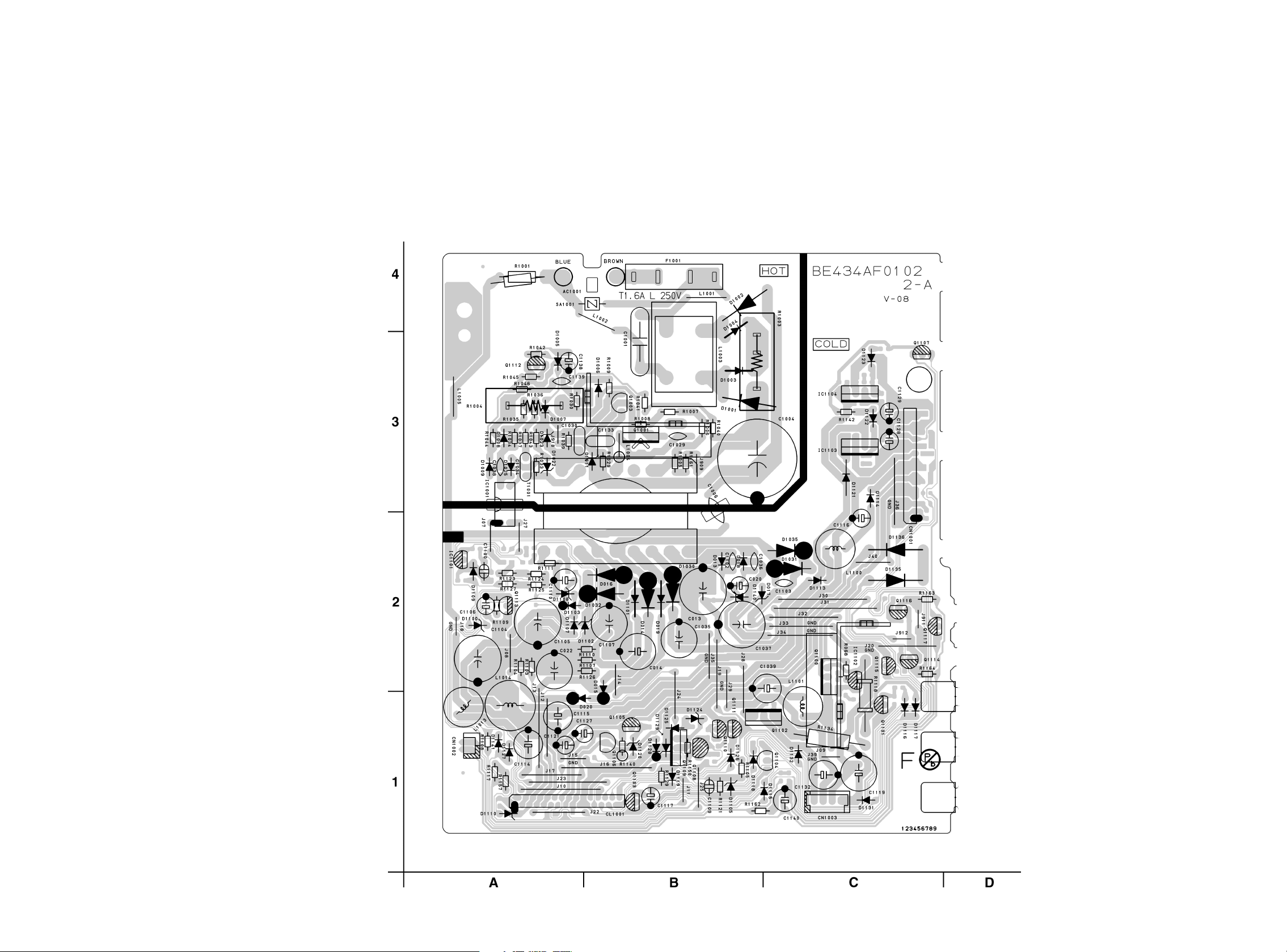
Page 34

Sub Power Supply Block Diagram
-FL
P-ON+15V
AL+16V/+12V
P-ON+9V(2)
AL+12V
AL+5V
P-ON+5V(DECK)
P-ON+9V(1)
AUDIO+5V
P-ON+5V(2)
AL+5V(1)
P-ON+5V
TIMER+5VF1F2
P-ON+5V(A)
EV+3.3V
AL+9V
TO SERVO/SYSTEM
AL+5V(2)
CONTROL
BLOCK DIAGRAM
TO SUB SYSTEM
CONTROL
BLOCK DIAGRAM
Q1509
Q1510
Q1501
Q1502
Q1511
Q1515
Q1504
+5V REG.
Q1518
+5V REG.
Q1516
Q1519
SW+3.3V
Q1517
+9V REG.
SW-CTL
1503
IC
Q1520
+5V REG.
P-ON-H
C-POW-SW
PWR-SW
LOW-POW
REG-CONT
FAN-LOCK
FAN-CONT1
AV CBA
CN1501
1 AL-30V
2 AL+44V
3,4 AL+16.3V
14 P-ON+9V(1)
7,8 AL+12V
AL+5V(3)
P-ON+5V(A)
23 F1
22 AL+5V
15,16
17,18
TO
POWER SUPPLY
BLOCK DIAGRAM
(CL1001)
24 F2
25 REG-CONT
26 LOW-POW
12 FAN-CONT1
27 PWR-SW
13 FAN-LOCK
1-12-10
E434GBLSP
Page 35

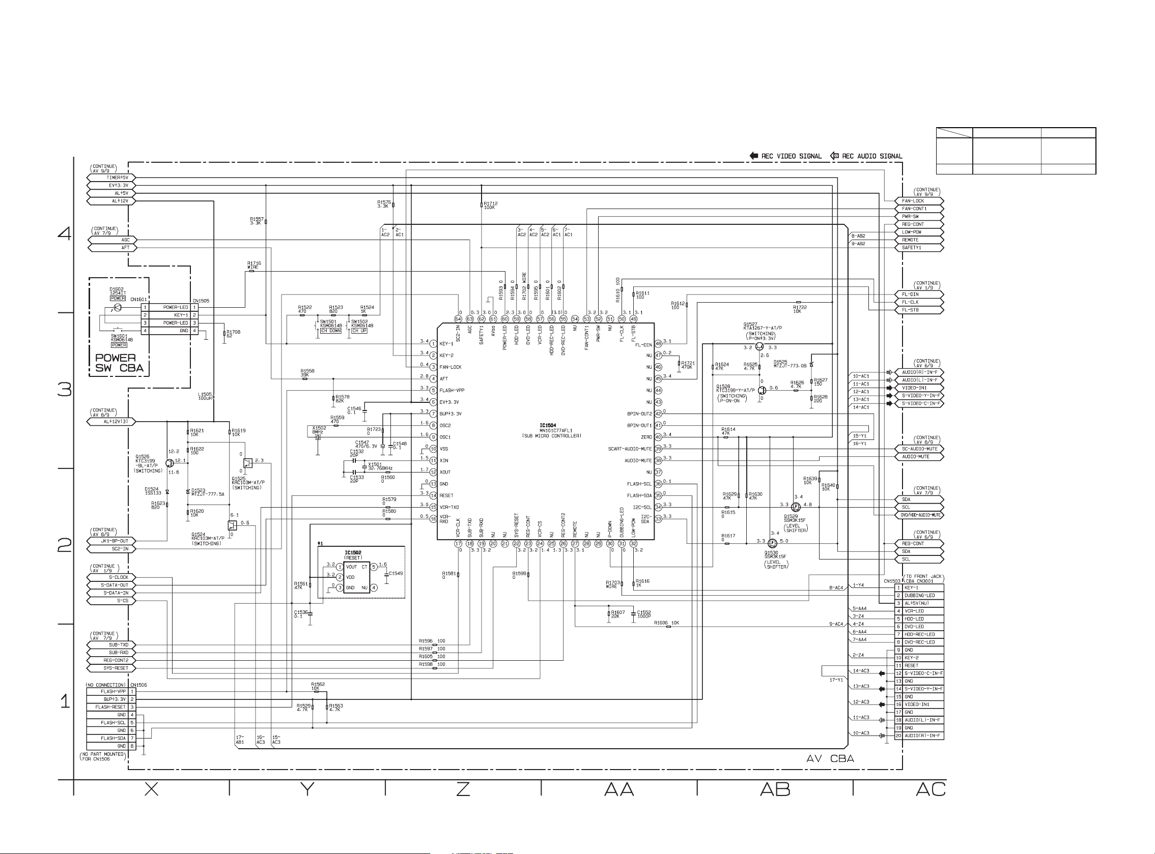
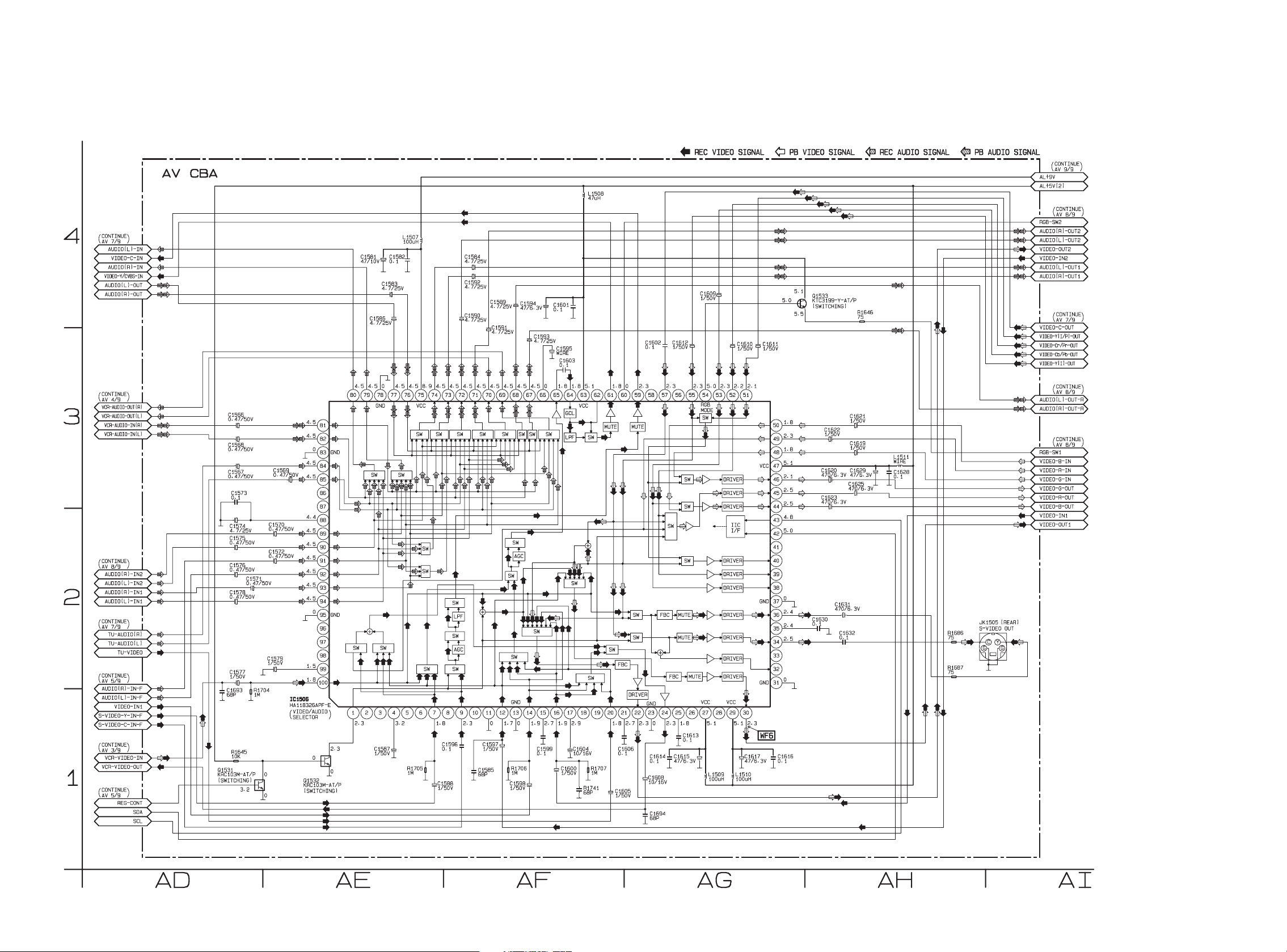
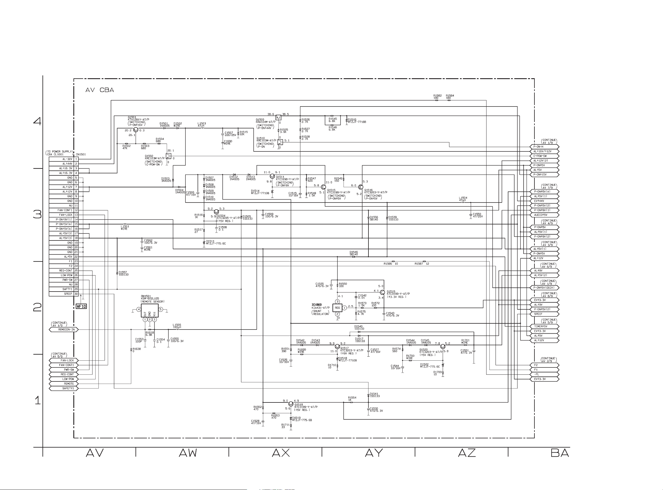
SCHEMATIC DIAGRAMS / CBA’S AND TEST POINTS
Standard Notes
WARNING
Many electrical and mechanical parts in this chassis
have special characteristics. These characteris tics
often pass unnoticed and the protection afforded by
them cannot necessarily be obtained by using
replacement components rated for higher voltage,
wattage, etc. Replacement parts that have these
special safety characteristics are identified in this
manual and its supplements; electrical components
having such features are identified by the mark " ! "
in the schematic diagram and the parts list. Before
replacing any of these components, read the parts list
in this manual carefully. The use of substitute
replacement parts that do not have the same safety
characteristics as specified in the parts list may create
shock, fire, or other hazards.
Notes:
1. Do not use the part number shown on these
drawings for ordering. The correct part number is
shown in the parts list, and may be slightly different
or amended since these drawings were prepared.
2. All resistance values are indicated in ohms
3
(K=10
3. Resistor wattages are 1/4W or 1/6W unless
otherwise specified.
4. All capacitance values are indicated in µF
(P=10
5. All voltages are DC voltages unless otherwise
specified.
6. Electrical parts such as capacitors, connectors,
diodes, IC’s, transistors, resistors, switches, and
fuses are identified by four digits. The first two
digits are not shown for each component. In each
block of the diagram, there is a note such as shown
below to indicate these abbreviated two digits.
, M=106).
-6
µF).
1-13-1 T2P_SC
Page 36

LIST OF CAUTION, NOTES, AND SYMBOLS USED IN THE SCHEMATIC DIAGRAMS ON
THE FOLLOWING PAGES:
1. CAUTION:
FOR CONTINUED PROTECTION AGAINST FIRE HAZARD, REPLACE ONLY WITH THE SAME TYPE FUSE.
2. CAUTION:
Fixed Voltage (or Auto voltage selectable) power supply circuit is used in this unit.
If Main Fuse (F1001) is blown, first check to see that all components in the power supply circuit are not
defective before you connect the AC plug to the AC power supply. Otherwise it may cause some components
in the power supply circuit to fail.
3. Note:
1. Do not use the part number shown on the drawings for ordering. The correct part number is shown in the
parts list, and may be slightly different or amended since the drawings were prepared.
2. To maintain original function and reliability of repaired units, use only original replacement parts which are
listed with their part numbers in the parts list section of the service manual.
4. Voltage indications for PLAY and REC modes on the schematics are as shown below:
< DVD/DVR Section >
231
5.0
The same voltage for
both PLAY & STOP modes
5.0
(2.5)
Indicates that the voltage
is not consistent here.
5. How to read converged lines
1-D3
Distinction Area
Line Number
(1 to 3 digits)
Examples:
1. "1-D3" means that line number "1" goes to the line number
"1" of the area "D3".
2. "1-B1" means that line number "1" goes to the line number
"1" of the area "B1".
6. Test Point Information
: Indicates a test point with a jumper wire across a hole in the PCB.
: Used to indicate a test point with a component lead on foil side.
: Used to indicate a test point with no test pin.
PLAY mode
STOP mode
< VCR Section >
5.0
The same voltage for
both PLAY, REC & DVD
modes
5.0
(2.5)
< >
PLAY mode
REC mode
DVD mode
231
Indicates that the voltage
is not consistent here.
3
AREA D3
2
1
AREA B1
1-D3
ABCD
Unit: Volts
1-B1
: Used to indicate a test point with a test pin.
1-13-2 W2P_SC
Page 37

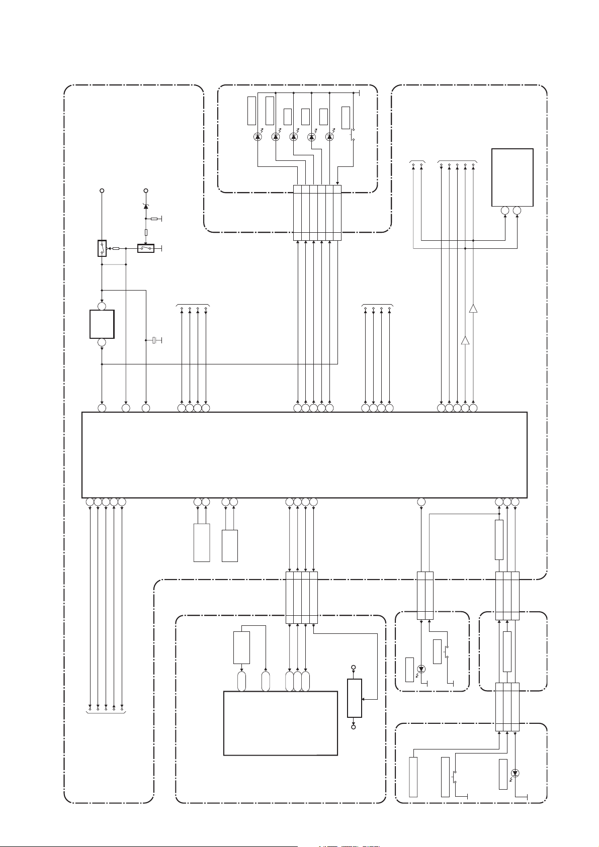
AV 1/9 Schematic Diagram < VCR Section >
1-13-3
E434GSCAV1
Page 38
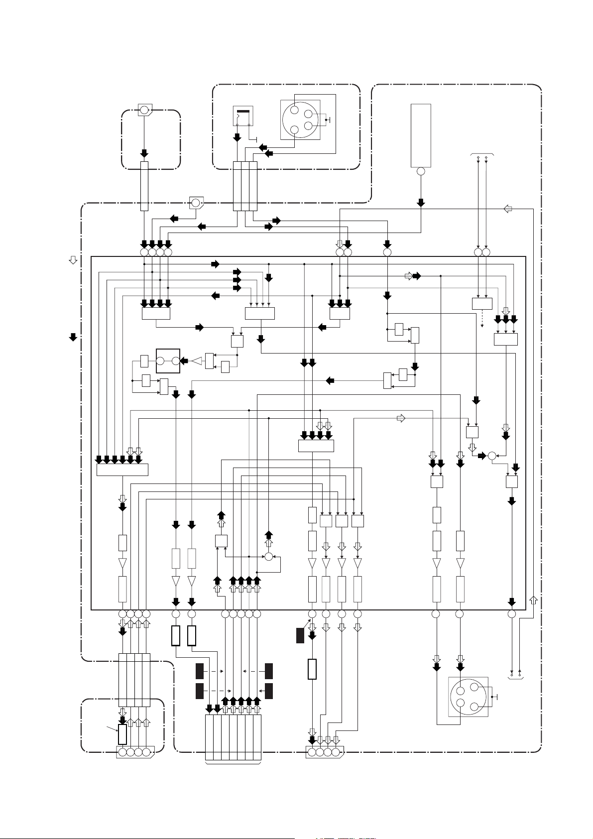
AV 2/9 & Sensor Schematic Diagram < VCR Section >
C
TIME
SHIFT
7G 6G 5G 4G 3G 2G 1G
a
b
c
d
e
f
g
c
d
e
ff
g
c
d
e
f
g
c
d
e
f
g
c
d
e
f
g
c
d
e
f
g
hh h
d
f
h
i
a
b
c
d
e
g
a
b
abababa
b
FL601 MATRIX CHART
CD
P-SCAN
DVD
PM
HDD
VCRDB
R
W
7G
6G
PM
h
5G 4G 3G 2G 1G
TIME
SHIFT
P-SCAN
h
DB
VCR
C
f
a
HDD
b
c
d
h
d
DVD
ef
g
CD
R
W
1-13-4
E434GSCAV2
Page 39
AV 3/9 Schematic Diagram < VCR Section >
1-13-5
E434GSCAV3
Page 40

AV 4/9 Schematic Diagram < VCR Section >
1-13-6
E434GSCAV4
Page 41
AV 5/9 & Power SW Schematic Diagram < VCR Section >
*1 NOTE
IC1502
R3112N191A-TR-FA
/R3112N191A-TR-FB
/BU4219G-TR
PST3619NR
Group A Group B
C1549 0.015 0.1
These components (IC1502, C1549)
can be used in any models.
However, you cannot mix components under
Group A with the ones under Group B.
You can choose either Group. The difference
between Group A and Group B is shown below.
1-13-7
E434GSCAV5
Page 42
AV 6/9 Schematic Diagram < VCR Section >
1-13-8
E434GSCAV6
Page 43

AV 7/9 Schematic Diagram < VCR Section >
1-13-9
E434GSCAV7
Page 44

AV 8/9 Schematic Diagram < VCR Section >
1-13-10
E434GSCAV8
Page 45
AV 9/9 Schematic Diagram < VCR Section >
1-13-11
E434GSCAV9
Page 46
Power Supply Schematic Diagram < VCR Section >
NOTE:
The voltage for parts in hot circuit is measured using
hot GND as a common terminal.
CAUTION !
Fixed voltage (or Auto voltage selectable) power supply circuit is used in this unit.
If Main Fuse (F1001) is blown , check to see that all components in the power supply
circuit are not defective before you connect the AC plug to the AC power supply.
Otherwise it may cause some components in the power supply circuit to fail.
CAUTION !
For continued protection against fire hazard,
replace only with the same type fuse.
1-13-12
E434GSCP
Page 47
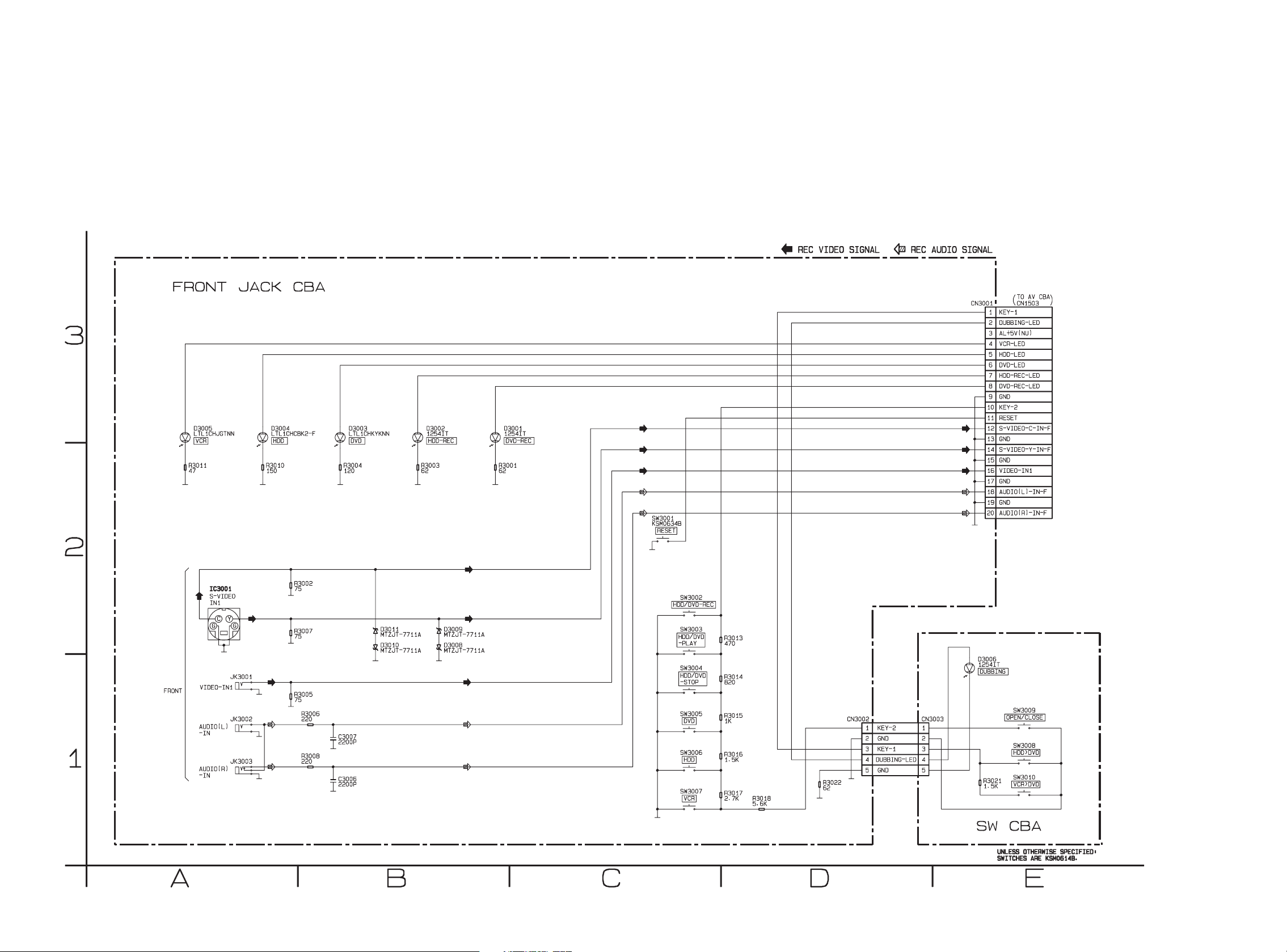
Front Jack & SW Schematic Diagram < VCR Section >
1-13-13
E434GSCFJ
Page 48
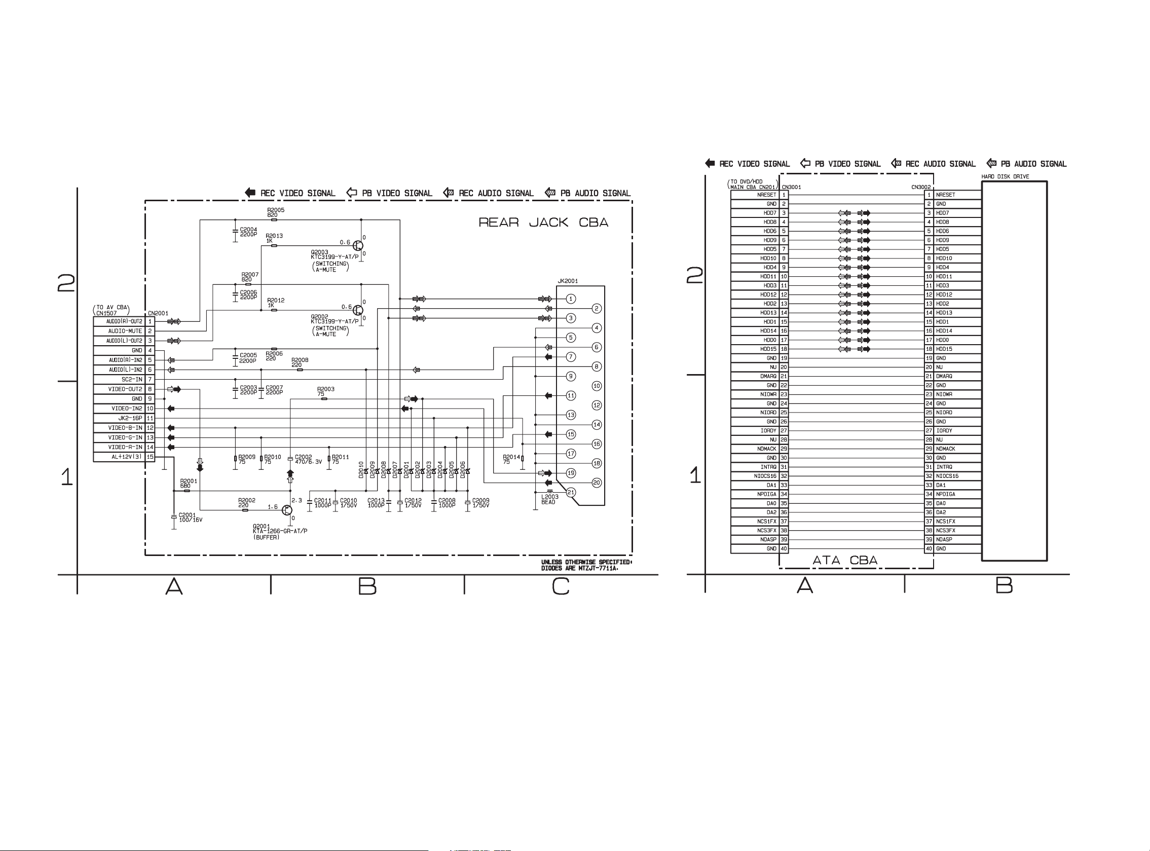
Rear Jack Schematic Diagram < VCR Section > ATA Schematic Diagram < DVD/HDD Section >
1-13-14
E434GSCRJ
E434GSCAT
Page 49

AFV Schematic Diagram < VCR Section >
1-13-15
E434GSCAFV
Page 50

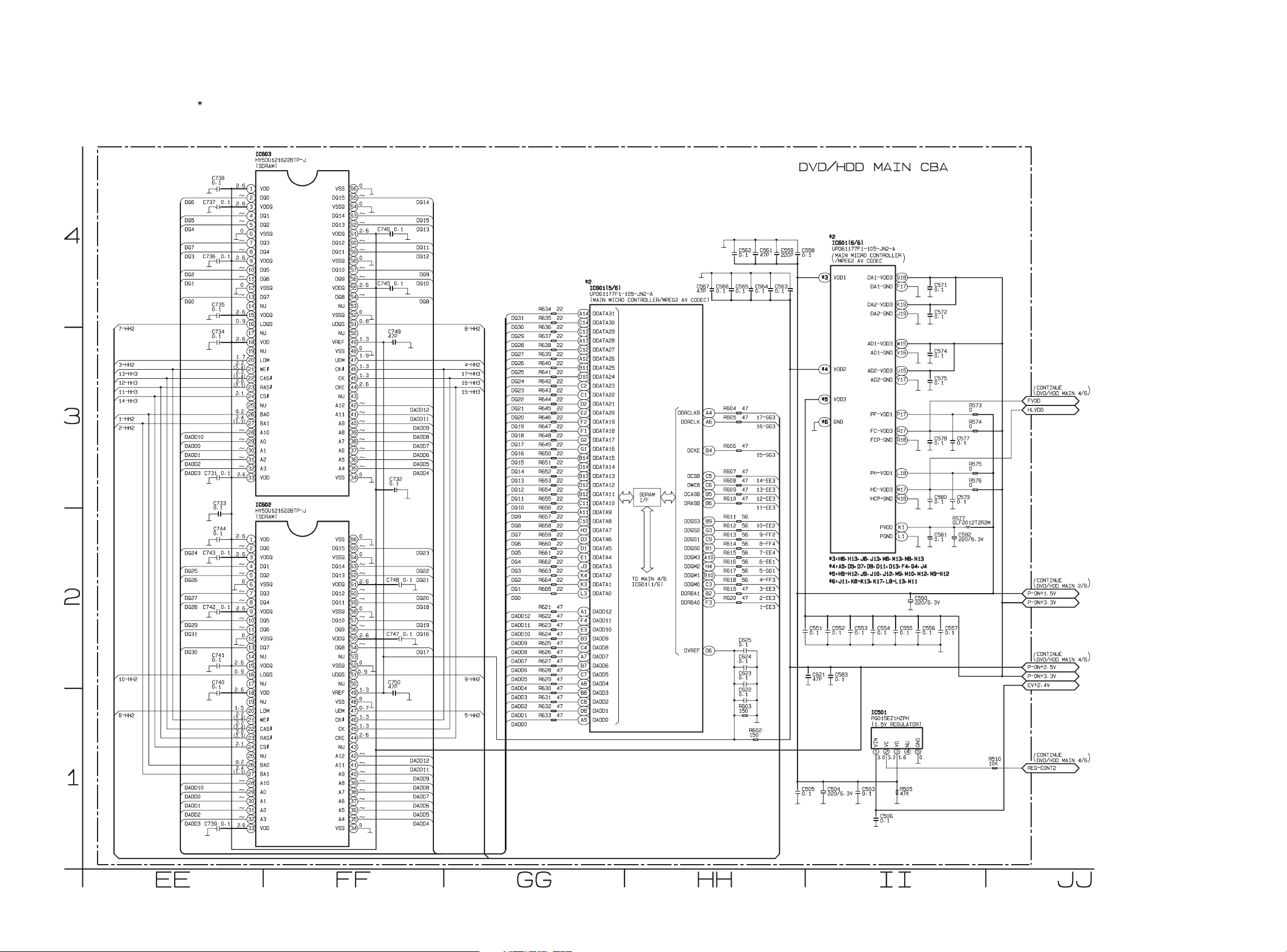
DVD/HDD MAIN 1/6 Schematic Diagram < DVD/HDD Section >
1-13-16
E434GSCD1
Page 51

DVD/HDD MAIN 2/6 Schematic Diagram < DVD/HDD Section >
1-13-17
E434GSCD2
Page 52

DVD/HDD MAIN 3/6 Schematic Diagram < DVD/HDD Section >
1-13-18
E434GSCD3
Page 53

DVD/HDD MAIN 4/6 Schematic Diagram < DVD/HDD Section >
2 NOTE:
The order of pins shown in this diagram is different from that of actual IC601.
IC601 is divided into six and shown as IC601 (1/6) ~ IC601 (6/6) in this DVD/HDD Main Schematic Diagram Section.
1-13-19
E434GSCD4
Page 54

DVD/HDD MAIN 5/6 Schematic Diagram < DVD/HDD Section >
2 NOTE:
The order of pins shown in this diagram is different from that of actual IC601.
IC601 is divided into six and shown as IC601 (1/6) ~ IC601 (6/6) in this DVD/HDD Main Schematic Diagram Section.
1-13-20
E434GSCD5
Page 55
DVD/HDD MAIN 6/6 Schematic Diagram < DVD/HDD Section >
2 NOTE:
The order of pins shown in this diagram is different from that of actual IC601.
IC601 is divided into six and shown as IC601 (1/6) ~ IC601 (6/6) in this DVD/HDD Main Schematic Diagram Section.
1-13-21
E434GSCD6
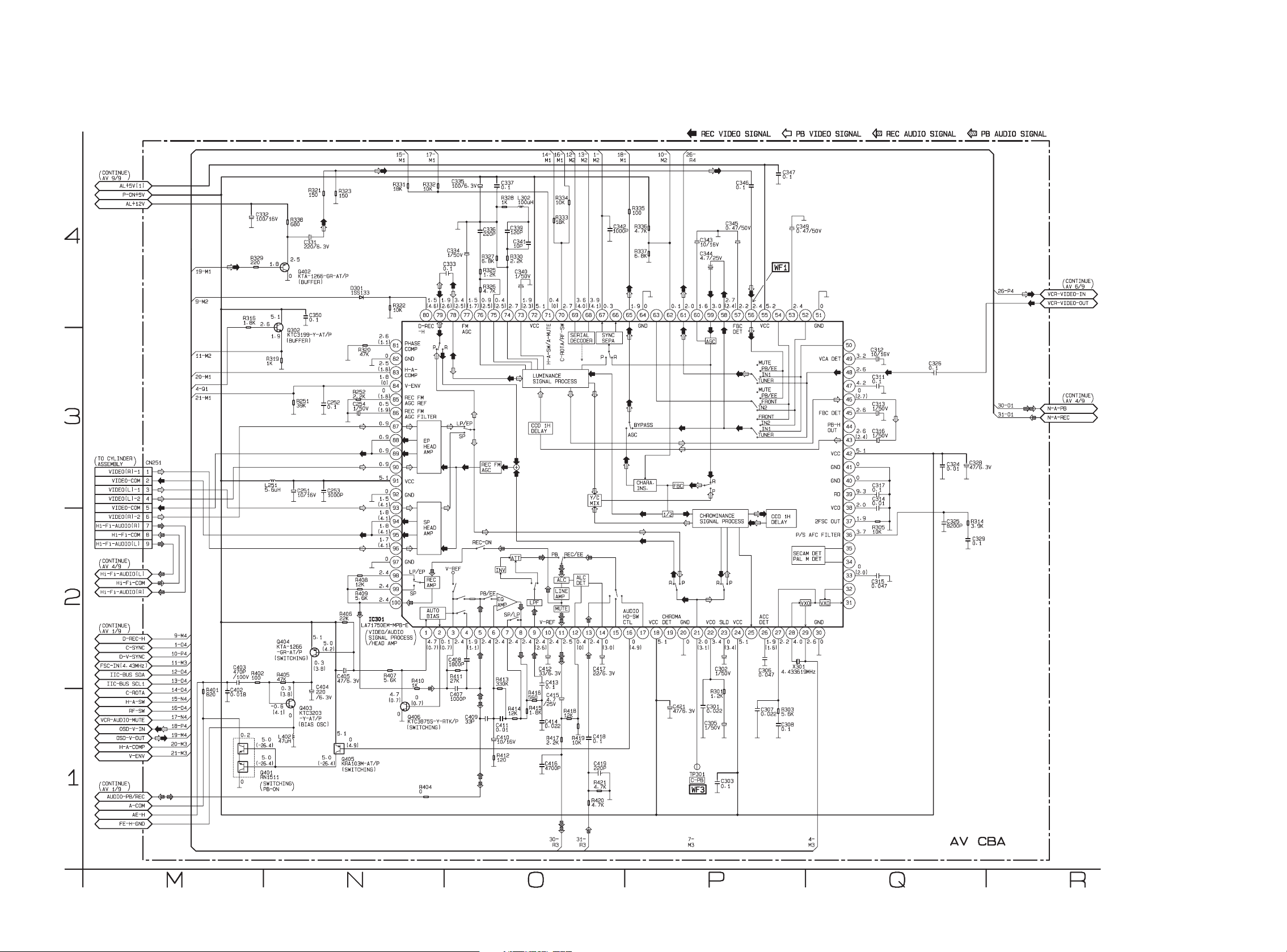
Page 56

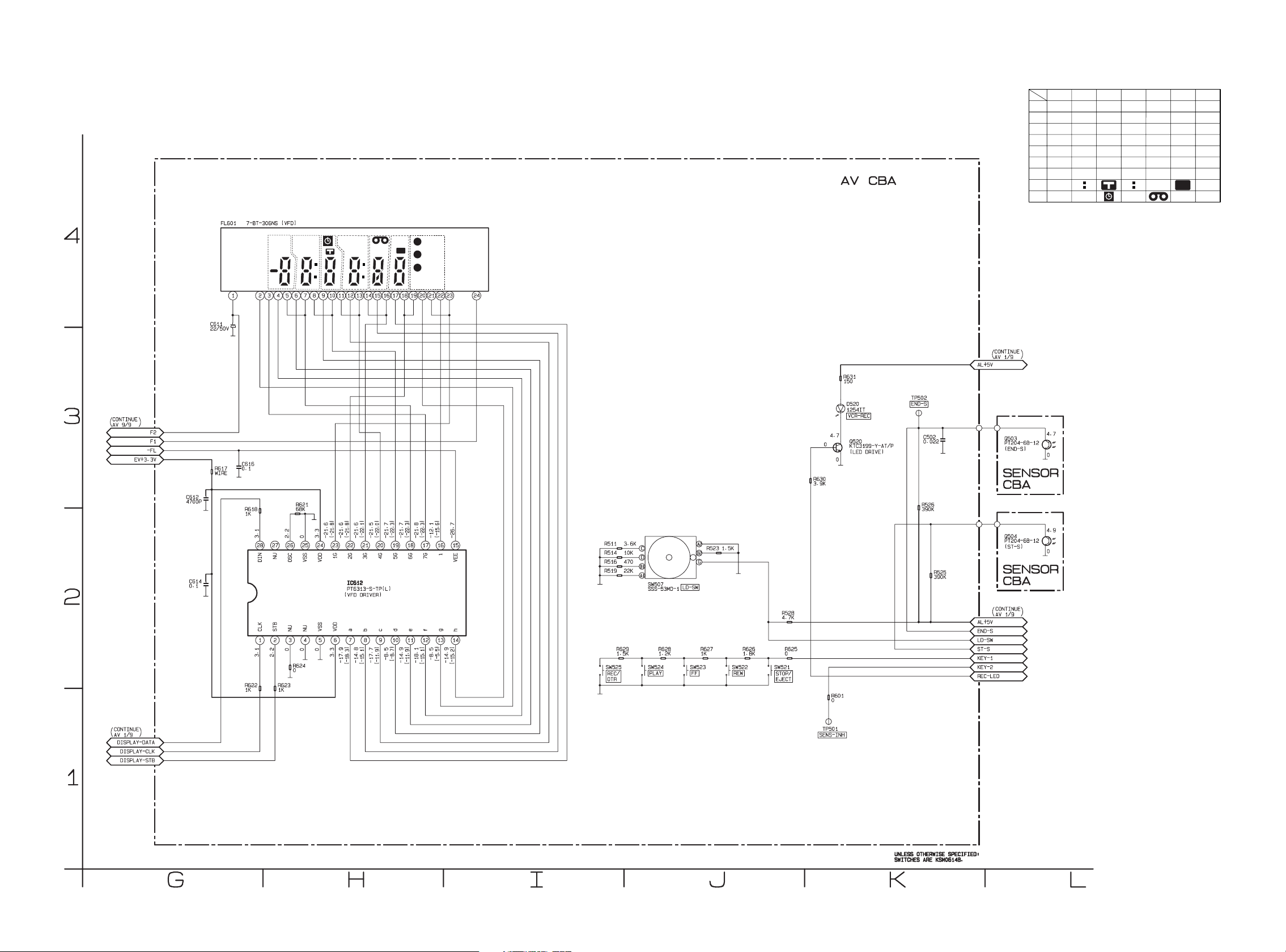
AV CBA Top View
Sensor CBA Top View
TP501
S-INH
WF2
WF2
TP504
TP504
RF-SW
RF-SW
VR501
SW-P
CTL
WF3
TP301
C-PB
TO SENSOR CBA
(END-SENSOR)
J340
JK2-V-OUT
BHF300F01012A
BHF300F01012B
TO SENSOR CBA (START-SENSOR)
1-13-22
BE434AF01015A
Page 57
AV CBA Bottom View
WF6
PIN 30 OF
IC1506
WF1
PIN 56 OF
IC301
WF8
PIN 3 OF
CN1504
WF7
PIN 5 OF
CN1504
WF4
PIN 7 OF
CN1504
WF5
PIN 9 OF
CN1504
WF9
PIN 17 OF
CN1504
WF10
PIN 30 OF
CN1501
1-13-23
BE434FA01015A
Page 58
Power Supply CBA Top View
Because a hot chassis ground is present in the power
supply circut, an isolation transformer must be used.
Also, in order to have the ability to increase the input
slowly, when troubleshooting this type power supply
circuit, a variable isolation transformer is required.
CAUTION !
For continued protection against fire hazard,
replace only with the same type fuse.
NOTE:
The voltage for parts in hot circuit is measured using
hot GND as a common terminal.
CAUTION !
Fixed voltage (or Auto voltage selectable) power supply circuit is used in this unit.
If Main Fuse (F1001) is blown , check to see that all components in the power supply
circuit are not defective before you connect the AC plug to the AC power supply.
Otherwise it may cause some components in the power supply circuit to fail.
1-13-24
BE434FA01022A
Page 59

Power Supply CBA Bottom View
CAUTION !
For continued protection against fire hazard,
replace only with the same type fuse.
NOTE:
The voltage for parts in hot circuit is measured using
hot GND as a common terminal.
CAUTION !
Fixed voltage (or Auto voltage selectable) power supply circuit is used in this unit.
If Main Fuse (F1001) is blown , check to see that all components in the power supply
circuit are not defective before you connect the AC plug to the AC power supply.
Otherwise it may cause some components in the power supply circuit to fail.
Because a hot chassis ground is present in the power
supply circut, an isolation transformer must be used.
Also, in order to have the ability to increase the input
slowly, when troubleshooting this type power supply
circuit, a variable isolation transformer is required.
1-13-25
BE434AF01022A
Page 60
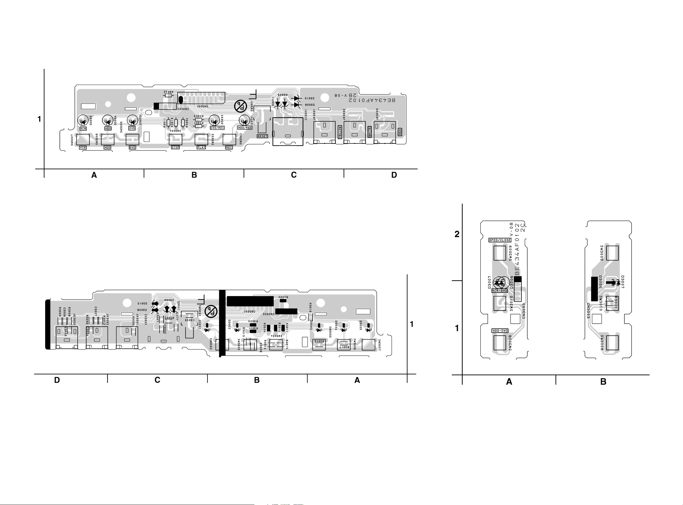
Front Jack CBA Top View
SW CBA Top View SW CBA Bottom View
Front Jack CBA Bottom View
BE434AF01022B
BE434AF01022C
1-13-26
Page 61

Rear Jack CBA Top View Rear Jack CBA Bottom View
Power SW CBA Top View Power SW CBA Bottom View
BE434AF01022D
ATA CBA Top View ATA CBA Bottom View
BE434AF01015B BE4340F01032
1-13-27
Page 62

AFV CBA Top View AFV CBA Bottom View
1-13-28
BE6800F01091
Page 63

WAVEFORMS
NOTE:
Input: COLOR BAR SIGNAL (WITH 1KHz AUDIO SIGNAL)
WF1
Pin 56 of IC301
V-OUT E-E 0.2V 20
WF1
WF2
UPPER
LOWER
Pin 56 of IC301
TP504
V-OUT 0.5V
RF-SW 5V
WF9
WF5
Pin 9 of CN1504
µs
50
µs
VIDEO-C 0.2V 20µs
WF6
Pin 30 of IC1506
VIDEO-CVBS 0.5V 20µs
Pin 17 of CN1504
AUDIO(L)-OUT
WF10
Pin 30 of CN1501
SPDIF 1V 0.1µs
1V 0.5ms
WF3
UPPER
WF2
LOWER
C-PB
RF-SW 5V 5m
WF4
Pin 7 of CN1504
TP301
TP504
0.2V
WF7
Pin 5 of CN1504
s
VIDEO-Cb
WF8
Pin 3 of CN1504
0.2V 20µs
VIDEO-Y 0.2V 20µs
VIDEO-Cr
0.2V 20µs
1-14-1
T2PWF
Page 64

Wiring 1/2 Diagram
TO
POWER
SUPPLY CBA
CL1001
1
2
4
6
8
10
11
12
13
14
AL-30V
CN1501
AL+44V
AL+16.3V3AL+16.3V
GND5GND
AL+12V7AL+12V
GND9GND
NU
FAN-CONT1
FAN-LOCK
P-ON+9V(1)
(W3)
15
16
AL+5V(3)17AL+5V(3)
P-ON+5V(A)
P-ON+5V(A)
WIRING DIAGRAMS
CONTINUE
WIRING
DIAGRAM 2/2
3
18
19
GND
21
GND20GND
22F123F224
AL+5V
26
27NU28
25
PWR-SW
LOW-POW
REG-CONT
29
30
SPDIF
CN1504
SAFFTY1
1
VIDEO-Y(I)-OUT
5
GND 2
GND 4
VIDEO-Cb/Pb-OUT
VIDEO-Cr/Pr-OUT
GND 6
7
GND 10
GND 8
VIDEO-Y(I/P)-OUT
AUDIO(R)-IN 11
VIDEO-C-OUT 9
GND 12
TO
GND 14
AUDIO(L)-IN 13
DVD/HDD
MAIN CBA
CN601
(W1)
15
17
GND 16
AUDIO(L)-OUT
AUDIO(R)-OUT
19
GND 18
DVD/HDD-AUDIO-MUTE
21
23
-IN
GND 22
AUDIO+5V 20
VIDEO-C
VIDEO-Y/CVBS-IN
25
GND 24
REG+CONT2 26
SUB-SCLK(NU)
27
29
RDY(NU) 28
SUB-TXD
SUB-RXD
SYS-RESET 30
ANT-IN
OPTICALCOAXIAL
DIGITAL AUDIO OUT
AUDIO(R)
-OUT
REAR
AUDIO(L)
-OUT
S-VIDEO
OUT
21
20
19
18
17
16
15
14
13
12
11
10
9
8
7
6
5
4
3
2
1
JK1504
(AV1)
CN1507
JW2001
AUDIO(L)-OUT2
AUDIO(R)-OUT2
11
CN2001
JK2201
AUDIO(R)-IN2
GND
AUDIO-MUTE
55
44
2 2
33
123456789
SENSOR CBA
9
SC2-IN
GND
AUDIO(L)-IN2
VIDEO-OUT2
77
9
66
88
REAR
JACK CBA
1011121314151617181920
SENSOR CBA
CN1
CN1508
AV CBA
CN504
AE-H
AE-H/FE-H
A-COM
AUDIO-PB/REC
CTL(+)
1
23456
CTL(-)
10
11
12
13
14
15
VIDEO-IN2
JK2-16P
VIDEO-B-IN
VIDEO-G-IN
VIDEO-R-IN
10
11
AL+12V(3)
12
13
14
15
21
AFV CBA
GND
NU
TU-AUDIO(R)
TU-AUDIO(L)
P-ON+5V(2)
P-ON+5V(2)
IIC-BUS-SCL
SIF
44
55
2 2
11
33
FE-H
FE-H GND
CN501
2
1
IIC-BUS-SDA
66
77
88
99
AL+16V/+12V
CN502
1
M
CAPSTAN
MOTOR
M
LOADING
MOTOR
POWER SW CBA
CN1601
W6
POWER-LED
POWER-LED
GND
KEY-1
11
44
33
2 2
CN1505
C-F/R
C-FG
C-CONT
P-ON+5V(DECK)
2
GND
4
3
5
6
MOTOR
DRIVE
D-CONT9D-PFG
LM-FWD/REV
8
7
CIRCUIT
GND
AL+12V(2)
10
11
S-VIDEO
IN1
1
2
CN3001
W4
DUBBING-LED
KEY-1
1
2
CN1503
P-ON+15V
12
CAPSTAN
FRONT
AUDIO(R)
VIDEO
-IN1
5
3
4
HDD-LED
AL+5V(NU)
VCR-LED
5
3
4
MOTOR
-IN
AUDIO(L)
-IN
8
6
7
DVD-REC-LED
DVD-LED
HDD-REC-LED
8
6
7
FRONT JACK CBA
9
10
11
13
12
14
GND
KEY-2
RESET
S-VIDEO-C-IN-F
GND
11
13
12
VIDEO-COM
VIDEO(L)-1
VIDEO(L)-2
VIDEO-COM
5
2
4
3
S-VIDEO-Y-IN-F
14
9
10
CN251
VIDEO(R)-1
1
2
1
CN3003
W7
GND
KEY-2
2
1
CN3002
15
16
17
GND
VIDEO-IN2
GND
15
16
17
VIDEO(R)-2
Hi-Fi-AUDIO(R)
Hi-Fi-COM
8
7
6
SW CBA
3
5
4
KEY-1
GND
DUBBING-LED
3
5
4
19
18
20
AUDIO(L)-IN-F
GND
AUDIO(R)-IN-F
19
18
20
Hi-Fi-AUDIO(L)
9
AUDIO
ACE HEAD
ASSEMBLY
(DECK ASSEMBLY)
ERASE
HEAD
AUDIO
HEAD
CONTROL
HEAD
FE HEAD
FULL
ERASE
HEAD
PG
SENSOR
CYLINDER
ASSEMBLY
M
DRUM
MOTOR
VIDEO
(R)1
HEAD
VIDEO
(L)1
HEAD
VIDEO
(L)2
HEAD
VIDEO
(R)2
HEAD
Hi-Fi
E434GWI11-15-1
AUDIO
(R) HEAD
Hi-Fi
AUDIO
(L) HEAD
Page 65

Wiring 2/2 Diagram
1
2
4
6
8
10
11
12
13
AV-30V
CL1001
AL+44V
AL+16.3V3AL+16.3V
GND5GND
GND9GND
AL+12V7AL+12V
NU
FAN-CONT1
FAN-LOCK
CONTINUE
WIRING
TO AV CBA
CN1501
(W3)
14
15
16
P-ON+9V(1)
P-ON+5V(A)
P-ON+5V(A)
DIAGRAM 1/2
18
19
GND
AL+5V(3)17AL+5V(3)
21
GND20GND
22F123F224
AL+5V
26
27
25
PWR-SW
LOW-POW
REG-CONT
28
NU
29
30
SPDIF
SAFFTY1
FAN 1
CN1002
2
CN1003
FAN-LOCK
FAN
W8
HDD+5V 1
HDD+12V 4
GND 2
GND 3
AC CORD
CN1001
SPDIF1
W2
CN501
SPDIF 1
GND2
EV+10.5V4
EV+10.5V5
GND3
EV+10.5V6
GND7
GND8
GND9
GND10
P-ON+5V11
P-ON+5V12
P-ON+5V13
EV+2.4V14
EV+2.4V15
EV+2.4V16
EV+2.4V17
GND18
GND19
P-ON+2.5V20
P-ON+2.5V21
P-ON+2.5V22
GND23
GND24
P-ON+3.3V25
P-ON+3.3V26
P-ON+3.3V27
GND28
GND29
GND30
1
CN601
GND 2
EV+10.5V 4
EV+10.5V 5
EV+10.5V 6
GND 7
GND 8
GND 9
GND 10
P-ON+5V 11
P-ON+5V 12
P-ON+5V 13
EV+2.4V 14
EV+2.4V 15
EV+2.4V 16
EV+2.4V 17
GND 3
GND 18
GND 19
P-ON+2.5V 20
P-ON+2.5V 21
P-ON+2.5V 22
GND 23
GND 24
P-ON+3.3V 25
P-ON+3.3V 26
P-ON+3.3V 27
GND 28
GND 29
GND 30
VIDEO-Y(I)-OUT
1
2456789
1
2456789
W5
1011121314151617183192021222324252627282930313233343536373839
1011121314151617183192021222324252627282930313233343536373839
5
GND 2
VIDEO-Cr/Pr-OUT3GND 10
GND 4
VIDEO-Cb/Pb-OUT
POWER SUPPLY CBA
7
VIDEO-C-OUT 9
GND 6
VIDEO-Y(I/P)-OUT
GND 8
HARD
DISK
DRIVE
ATA CBA
CONTINUE
WIRING DIAGRAM 1/2
TO AV CBA
CN1504
(W1)
15
17
19
21
25
GND 12
AUDIO(L)-IN 13
GND 14
GND 16
AUDIO(R)-OUT
AUDIO(L)-OUT
GND 18
DVD/HDD-AUDIO-MUTE
AUDIO+5V 20
VIDEO-Y/CVBS-IN
GND 22
VIDEO-C-IN 23
GND 24
SUB-SCLK(NU)
REG-CONT2 26
SUB-TXD27RDY(NU) 28MSUB-RXD29SYS-RESET 30
40
40
AUDIO(R)-IN 11
DVD/HDD MAIN CBA
NRESET 1
GND 2
HDD8 4
HDD6 5
HDD9 6
HDD5 7
HDD10 8
HDD4 9
HDD11 10
HDD3 11
HDD12 12
HDD2 13
HDD13 14
HDD1 15
HDD14 16
HDD0 17
HDD7 3
HDD15 18
GND 19
NU 20
DMARQ 21
GND 22
NIOWR 23
GND 24
NIORD 25
GND 26
IORDY 27
NU 28
NDMACK 29
GND 30
INTRQ 31
NIOCS16 32
DA1 33
NPDIGA 34
DA0 35
DA2 36
NCS1FX 37
NCS3FX 38
NDASP 39
GND 40
CN401
CN1001
DVD MECHANISM
DVD MECHANISM & DVD/HDD MAIN CBA UNIT
118
217
VH-
HW-
CN1003
316
HW+
123
SLED
415
514
HV-
HV+
SENSOR
ENCODER CBA
613
HU-
RELAY
712
HU+
CBA
811
VCC
910 U
TRAY
109
V
OPEN
118W127
T-SCN3
CN1002
LOADER CBA
136
145
T-SCN2
GND
~
1
SPINDLE
154
SL+
11
MOTOR
163
SL-
172
SW1
M
SLED
MOTOR
CN101 CN3001CN201 CN3002
FCS(+) 4TRK(-)
1
2 FCS(-)
FOCUS
ACTUATOR
PICK-UP
TRK(+)
3
TRACKING
ACTUATOR
5 TILT(+)
TILT
GND9GND
6 TILT(-)
7
ACTUATOR
FPD
THERMO
8
10
1-15-2
FPD-SW
VC-PD15H16D17C18F19NU20NU21SW22RF(+)23RF(-)24E25B26A27G28GND29VCC230IIN331IIN232IIN133GND34XOUTEN335GND36XOUTEN237GND38OSCEN39LDEN240LDEN1
VCC1
VC-FPD
11
12
14
13
FPDIC
PDIC
DVD-LD
DVD/CD
LASER
DIODE
DRIVE
CD-LD
E434GWI2
Page 66

IC PIN FUNCTION DESCRIPTIONS
< VCR Section >
IC501( SERVO / SYSTEM CONTROL IC )
Pin
IN/
No.
OUT
12IN
3 IN POW-SAF Abnormal Voltage Detection
4IN
56IN
7IN
8IN
9IN
10 IN
11 -
12 13 OUT
14 IN
15 OUT
16 OUT
17 IN
18 OUT
19 OUT
20 -
21 22 23 24 25 26 OUT REC-LED
27 28 29 30 -
31 IN
32 IN
Signal
Name
NU Not Used
PG-DELAY
END-S
NU Not Used
V-ENV
KEY-1 Key Scan Input Signal 1
KEY-2 Key Scan Input Signal 2
LD-SW
ST-S
NU Not Used
NU Not Used
D-V- SYNC Dummy V-sync Output
REMOCON
-IN
C-ROTA
H-A-SW
H-A-COMP Head Amp Comparator Signal
RF-SW Video Head Switching Pulse
Hi-Fi-H-SW
NU Not Used
NU Not Used
NU Not Used
NU Not Used
NU Not Used
NU Not Used
NU Not Used
NU Not Used
NU Not Used
NU Not Used
REC-SAFSW
A-MODE Hi-Fi Tape Detection Signal
Video Head Switching Pulse
Signal Adjusted Voltage
Tape End Position Detect
Signal
Video Envelope Comparator
Signal
Deck Mode Position Detector
Signal
Tape Start Position Detector
Signal
Remote Control Sensor
Color Phase Rotary
Changeover SIgnal
Video Head Amp Switching
Pulse
HiFi Audio Head Switching
Pulse
Rec Mode LED Signal Output
Recording Safety SW Detect
(With Record tab=”L”/ With out
Record tab=”H”)
Function
Pin
IN/
No.
OUT
33 OUT
34 IN
35 IN
36 OUT
37 38 IN
39 OUT
40 41 42 43 IN
44 IN
45 OUT
46 47 IN
48 IN
49 -
50 IN
51 -
52 OUT
53 54 55 -
56 57 -
58 IN
59 -
60 OUT
61 -
62 63 -
64 IN S-CS
65 OUT
66 IN
67 OUT
D-REC-H Delayed Record Signal
RESET
Xcin Sub Clock
Xcout Sub Clock
Vcc Vcc
Xin Main Clock Input
Xout Main Clock Input
GND Vss(GND)
NU Not Used
NU Not Used
CLKSEL Clock Select (GND)
OSCin Clock Input for letter size
OSCout Clock Output for letter size
NUB Not Used
LP LP
FSC-IN
[4.43MHz]
OSDVss OSDVss
OSD-V-IN OSD Video Signal Input
LECHA Not Used
OSD-V-
OUT
OSDVcc OSDVcc
HLF
NU Not Used
NU Not Used
NU Not Used
C-CYNC
NU Not Used
C-POW-SW
NU Not Used
NU Not Used
NU Not Used
S-DATAOUT
S-DATA-IN
S-CLOCK
Signal
Name
Function
System Reset Signal
(Reset=”L”)
4.43MHz Clock Input
OSD Video Signal Output
LPF Connected Terminal
(Slicer)
Composite Synchronized
Pulse
Capstan Power Switching
Signal
Sub Micro Controller Interface
Chip Select Signal Input
Communication of Data from
VCR Micro Controller
Communication of Data to
VCR Micro Controller
Communication of Clock with
VCR Micro Controller
1-16-1 E434GPIN
Page 67

Pin
IN/
No.
OUT
68 OUT
69 OUT
70 OUT
71 OUT
IN/
72
OUT
73 74 75
OUT P-ON-H Power On Signal to High
76 OUT
77 OUT
78 OUT
79 IN
80 IN
81 OUT
82 -
83 OUT
84 85 86 -
87 IN
88 -
89 - GND GND
90
IN
91 -
92 93 -
IN/
94
OUT
IN/
95
OUT
96 -
97 98 99 -
100
Signal
Name
DRV-DATA VFD Driver IC Control Data
DRV-STB
DRV-CLK VFD Driver IC Control Clock
IIC-BUSSCL
IIC-BUSSDA
NU Not Used
NU Not Used
C-CONT Capstan Motor Control Signal
D-CONT Drum Motor Control Signal
C-F/R
S-REEL Supply Reel Rotation Signal
T-REEL Take Up Reel Rotation Signal
LM-FWD/
REV
NU Not Used
VCR-
AUDIOMUTE
NU Not Used
NU Not Used
NU Not Used
C-FG
AMPVss AMPVss
D-PFG
AMPVREF
out
AMPVREF
in
P80/C P80/C Terminal
CTL (-)
CTL (+)
AMPC
CTL
AMPVcc AMPVcc
AVcc
-
NU Not Used
VFD Driver IC Chip Select
Signal
IIC BUS Control Clock
IIC BUS Control Data
Capstan Motor FWD/REV
Control Signal (FWD=“L”/
REV=“H”)
Loading Motor Control Signal
Audio Mute Control Signal
(Mute = “H”)
Capstan Motor Rotation
Detection Pulse
Drum Motor Phase/
Frequency Generator
V-Ref for CTL AMP
V-Ref for CTL AMP
Playback/Record Control
Signal (-)
Playback/Record Control
Signal (+)
CTL AMP Connected
Terminal
To Monitor for CTL AMP
Output
A/D Converter Power Input/
Standard Voltage Input
Function
Notes:
Abbreviation for Active Level:
PWM -----Pulse Wide Modulation
A/D--------Analog - Digital Converter
IC612 (FRONT PANEL CONTROL)
Pin
IN/
No.
OUT
1 IN CLK Clock Input
2 IN STB Serial Interface Strobe
3 - NU Not Used
4 - NU Not Used
5- VSS GND
6- VDD Power Supply
7OUT a
8OUT b
9OUT c
10 OUT d
11 OUT e
12 OUT f
13 OUT g
14 OUT h
15 - VEE Pull Down Level
16 OUT i Segment Output
17
18 6G
19 5G
OUT
20 4G
21 3G
22 2G
23 1G
24 - VDD Power Supply
25 - VSS GND
26 IN OSC Oscillator Input
27 - NU Not Used
28 IN DIN Serial Data Input
7G
Signal
Name
Function
Segment Output
Grid Output
1-16-2 E434GPIN
Page 68

LEAD IDENTIFICATIONS
E C B
MID-32A22F
PT204-6B-12
C
E
KRC106M-AT/P
1: B
2: C
3: E
1 2 3
MSP3417G-QG-B8-V3
33
34
KRA103M-AT/P
KRA104M-AT/P
KRC103M-AT/P
KTA-1266-GR-AT/P
KTA1267-(GR,Y)-AT/P
KTA1281Y-AT/P
KTC3193-Y-AT/P
KTC3199-(GR,BL,Y)-AT/P
RN1206
PQ070XF01SZH
1234
SSM3K15F(TE85L F)
23
22
2SA1015-GR(TE2 F T)
2SA1020-Y(TE6 F M)
2SC1815-(BL,GR,Y)(TE2 F T)
2SC2120-(Y)(TE2 F T)
2SC3266-(GR,Y)(TPE2 F)
KTC3203-Y-AT/P
KTC3205-Y-AT/P
KTC3198-(GR,Y)-AT/P
KTC3266-(GR,Y)-AT/P
E C B
PT6313-S-TP(L)
SC16313G
28
1
D
GS
LA72648M-MPB-E
60
61
15
14
KIA4558P/P
RC4580IP
UTC4580 DIP-8
8 5
1 4
S2Y52
B C E
KTC2026-Y/P
KRC103S-RTK/P
KTC3875S-(GR,Y)-RTK/P
C
BE
41
EL817A
EL817B
40
PS2561A-1(Q)
PS2561A-1(W)
KIA431-AT/P
1: R
2: A
3: K
123
2SK3798(Q)
BCE
GDS
BU4219G-TR
PST3619NR
R3112N191A-TR-FA
R3112N191A-TR-FB
54
123
44
49
64
1
MN101C77A FL1
48
1
33
16
11
32
17
12
81
100
80
1
HA118326APF-E
LA71750EM-MPB-E
M3776AMCH-AE9GP
80
1
1-17-1 E434GLE
20
51
30
21
1
2
FMG4A T148
RN1511(TE85R.F)
50
31
C1 C2
B1 E B2
1: Anode
4
2: Cathode
3
3: Emitter
4: Collector
Note:
A: Anode
K: Cathode
E: Emitter
C: Collector
B: Base
R: Reference
S: Source
G: Gate
D: Drain
Page 69
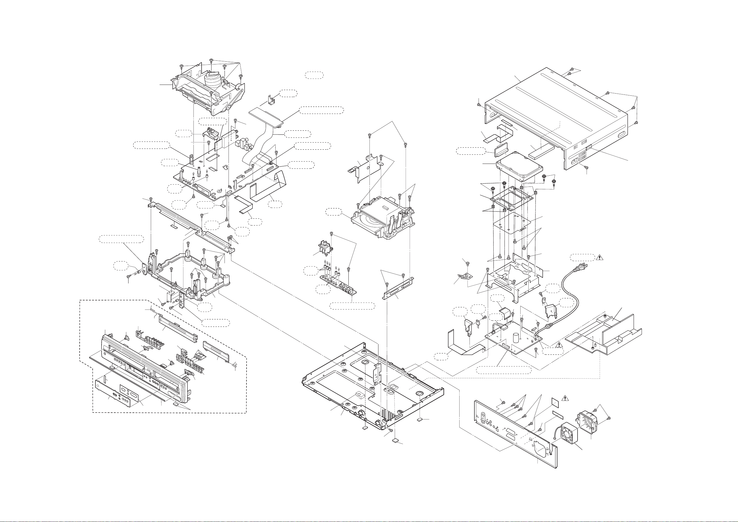
Cabinet
1B1
L-12
A,B,C,D,E
B-24
EXPLODED VIEWS
See Electrical Parts List
for parts with this mark.
L-1
A
A-3
L-1
B,C
L-1
D,E, F
Power SW CBA
B-9
G
L-6
A-1X
Front Assembly
A1X-17
A1X-1
A1X-3
A1X-15
A1X-8
Sensor CBA
L-6
A
E
A1X-11
A1X-4
A1X-14
B-18
A1X-9
A1X-5
B-31
B-14
L-10
A
L-6
F
A1X-12
A1X-13
B-9
H,I
B-11
L-6
L-9
B
B-10
L-9
A
P
L-10
L-6
L-10
B
F,G , H
G
A1X-6
A,B,C
A1X-7
A1X-18
AFV CBA
B-16
L-9
Q
L-2
B
B-8
B-9
F
SW CBA
A1X-2
A1X-10
A,B
L-10
C,D,E
A1X-16
L-2
A
L-9
G,H
L-9
B
W4
L-9
C,D
W1
Rear Jack CBA
JW2001
Sensor CBA
AV CBA
B-2
B-9
A,B,C
1B2
B-9
D,E
Front Jack CBA
B-12
B-20
A-2
B-3
L-9
E,F
A-7
A
L-8
A,B
L-8
L-6
C,D
W5
B-4
B-15
ATA CBA
L-7
A,B
L-11
A,B
1B3
L-15
A,B
B-22
C,D
L-15L-15
C,D
L-1
G
B-19
B-21
B-22
L-9
R
A,B
L-13
A,B
B-32
L-13
C,D
L-9
K
AC1001
B-1
L-9
O
B-5
B
M
A-16
B-13
B-7
B-5
A
L-9
I,J
L-9
W3
L-9
N
W8
L
L-5
A
L-9
F1001
W2
L-5
B
Power Supply CBA
L-3
L-16
A,B,C
L-4
D
A,B
A-10
L-4
A,B
A-9
A-5
L-4
C
A-7
B
C
A-11
FM1001
A-4
1-18-1 E434GCEX
Page 70

Packing [HDR-A2835D]
X1
S-1
X-3B
X-3A
X-3D
X-3C
X-1
X-3F
X-3E
X-3G
X-2B X-26
X-2A
X-5 X-6
Upper SideLower Side
X-22
X-7
S-10
S-5
S-6
A-22
S-3
S-1
A-9
S-7
S-2
1-18-2 E434GPEX
Page 71
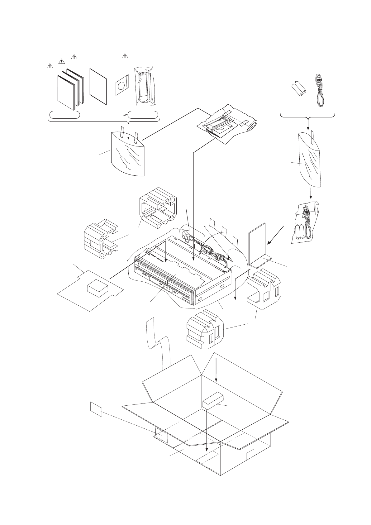
Packing [HDR-B2735D]
X-2A
X-2B
X-2
X1X26X-3
X-5 X-6
Upper SideLower Side
X-1
X-7
S-11
S-1
S-5
S-6
A-22
S-3
S-1
A-9
S-7
S-2
1-18-3 E434GPEX
Page 72

MECHANICAL PARTS LIST
PRODUCT SAFETY NOTE: Products marked with a
! have special characteristics important to safety.
Before replacing any of these components, read
carefully the product safety notice in this service
manual. Don't degrade the safety of the product
through improper servicing.
NOTE: Parts that are not assigned part numbers
(---------) are not available.
Comparison Chart of Models and Marks
Model Mark
HDR-A2835D A
HDR-B2735D B
Ref. No. Mark Description Part No.
A-1X FRONT ASSEMBL Y E434FED 1VM222690
A-2 MAIN CHASSIS E4340UD 1VM120193H
A-3 TOP COVER E4340UD 1VM020090F
A-4 REAR PANEL E434FED 1VM222697
A-5 F AN HOLDER E4340UD 1VM220745
A-7A FOOT E650 0UD 0VM416122
A-7B FOOT E650 0UD 0VM416122
A-9 A BARCODE LABEL E434GED ---------A-9 B BARCODE LABEL E434JBD ---------A-10 A RA TI NG LABEL E4 34GED ---------A-10 B RA TI NG LABEL E4 34JBD ---------A-11 CENTER CUSHION E4350JD 1VM422956
A-16 POWER HOLDER E434AED 1VM322233
A-22 TOP PER POP E434FED 1VM323234
A1X-1 FRONT PANEL E434FED 1VM222689
A1X-2 TRA Y PANEL E434AED 1VM423384
A1X-3 POWER LENS E4340UD 1VM321075
A1X-4 VCR REC LENS E4340UD 1VM321076
A1X-5 DUBBING LENS E4340UD 1VM32 1077
A1X-6A MODE LENS E4340UD 1VM321078
A1X-6B MODE LENS E4340UD 1VM321078
A1X-6C MODE LENS E434 0UD 1VM321078
A1X-7 HDD/DVD REC LENS E4340UD 1VM321079
A1X-8 DISPLA Y WINDOW E434AED 1VM322197
A1X-9 CASSETTE DOOR E434AED 1VM423385
A1X-10 MODE BUTTON E434AED 1VM423386
A1X-11 POWER BUTT ON E434AED 1VM423387
A1X-12 OPEN BUTTON E434AED 1VM423388
A1X-13 CENTER ORNAMENT E4340UD 1VM422053
A1X-14 ADHESIVE T APE A E4340UD 1VM422054
A1X-15 ADHESIVE T APE B E4340UD 1VM422055
A1X-16 TRA Y SPRING E6510JD 0VM416265
A1X-17 DOOR SPRING HF410UD 1VM421240
A1X-18A FOOT E6500UD 0VM416122
A1X-18B FOOT E6500UD 0VM416122
1B1 DECK ASSEMBLY CZD014/VM25E0 N25E1FL
1B3 ST3160212ACE ST3160212ACE or UHDD160VE002
HARD DISK DRIVE 160GB WD1600BB55RDA0 or
HARD DISK DRIVE ST3160022ACE or UHDD160VE001
HARD DISK DRIVE WD1600BB-55GUC0 UHDD160WG001
B-1 HDD BRACKET E4340 UD 1VM220719D
B-2 MODE LENS HOLDER E4340UD 1VM422056
B-3 WIRE SHEET E43 40UD 1VM321081
B-4 TAPE HIMELON(HDD) E4340UD 1VM422058
B-7 EARTH PLATE E4321JD D V -HD300 0VM414677A
B-8 DECK PEDESTAL E9600UD 1VM120055D
B-11 FRONT BRACKET E9400UD 0VM204534C
UHDD160WG002
Ref. No. Mark Description Part No.
B-12 FRONT BRA CKET R E9400UD 0VM416269A
B-13 BRACKET R E9600UD 1VM421062F
B-14 TAPE HIMELON H9206JD 0VM413956
B-15 RUBBER CUSHION(T OP CO VER)
B-18 FRONT SUPPOR T E4340UD 1VM422518
B-19 SIDE CUSHION(TOP COVER) E4340UD 1VM422517
B-20 RUBBER CUSHION (MAIN CHASSIS)
B-21 HDD SUPPORT E3A50JD 1VM424843
B-22A HDD RUBBER E4350JD 1VM422863
B-22B HDD RUBBER E4350JD 1VM422863
B-22C HDD RUBBER E4350JD 1VM422863
B-22D HDD RUBBER E4350JD 1VM422863
B-32 INSULATION SHEET E434AED 1VM424477
FM1001 DC F AN MOTOR 2410RL-04W-S20-C01 orMMEZR12NM005
L-1A SCREW C-TIGHT M3X5 BIND HEAD + GBCC3050
L-1B SCREW C-TIGHT M3X5 BIND HEAD + GBCC3050
L-1C SCREW C- TIGHT M3X5 BIND HEAD + GBCC3050
L-1D SCREW C- TIGHT M3X5 BIND HEAD + GBCC3050
L-1E SCREW C-TIGHT M3X5 BIND HEAD + GBCC3050
L-1F SCREW C-TIGHT M3X5 BIND HEAD + GBCC3050
L-1G SCREW C-TIGHT M3X5 BIND HEAD + GBCC3050
L-3A SCREW B-TIGHT M3X8 BIND HEAD+ GBHB30 80
L-3B SCREW B-TIGHT M3X8 BIND HEAD+ GBHB30 80
L-3C SCREW B-TIGHT M3X8 BIND HEAD+ GBHB3080
L-4A SCREW S-TIGHT M3*5 BIND+ 3*5
L-4B SCREW S-TIGHT M3*5 BIND+ 3*5
L-4C SCREW S-TIGHT M3*5 BIND+ 3*5
L-4D SCREW S-TIGHT M3*5 BIND+ 3*5
L-5A SCREW P-TIGHT M3X6 BIND HEAD+ G BJP3060
L-5B SCREW P-TIGHT M3X6 BIND HEAD+ G BJP3060
L-6A SCREW P-TIGHT M3X8 BIND HEAD+ G BJP3080
L-6B SCREW P-TIGHT M3X8 BIND HEAD+ G BJP3080
L-6C SCREW P-TIGHT M3X8 BIND HEAD+ GBJP3080
L-6D SCREW P-TIGHT M3X8 BIND HEAD+ GBJP3080
L-6E SCREW P-TIGHT M3X8 BIND HEAD+ G BJP3080
L-6F SCREW P-TIGHT M3X8 BIND HEAD+ GBJP3080
L-6G SCREW P-TIGHT M3X8 BIND HEAD+ GBJP3080
L-7A SCREW P-TIGHT M3*12 BIND+ GBJP3120
L-7B SCREW P-TIGHT M3*12 BIND+ GBJP3120
L-8A SCREW M3X5 HEAD+ BIND S-TIGHT GBJS3050
L-8B SCREW M3X5 HEAD+ BIND S-TIGHT GBJS3050
L-8C SCREW M3X5 HEAD+ BIND S-TIGHT GBJS3050
L-9A SCREW S-TIGHT M3X6 BIND HEAD+ G BJS3060
L-9B SCREW S-TIGHT M3X6 BIND HEAD+ G BJS3060
L-9C SCREW S-TIGHT M3X6 BIND HEAD+ GBJS3060
L-9D SCREW S-TIGHT M3X6 BIND HEAD+ GBJS3060
L-9E SCREW S-TIGHT M3X6 BIND HEAD+ G BJS3060
L-9F SCREW S-TIGHT M3X6 BIND HEAD+ GBJS3060
L-9G SCREW S-TIGHT M3X6 BIND HEAD+ GBJS3060
L-9H SCREW S-TIGHT M3X6 BIND HEAD+ GBJS3060
L-9I SCREW S-TIGHT M3X6 BIND HEAD+ GBJS3060
L-9J SCREW S-TIGHT M3X6 BIND HEAD+ GBJS3060
L-9K SCREW S-TIGHT M3X6 BIND HEAD+ GBJS3060
L-9L SCREW S-TIGHT M3X6 BIND HEAD+ GBJS3060
L-9M SCREW S-TIGHT M3X6 BIND HEAD+ GBJS3060
L-9Q SCREW S-TIGHT M3X6 BIND HEAD+ GBJS3060
L-9R SCREW S-TIGHT M3X6 BIND HEAD+ GBJS3060
L-10A SCREW S-TIGHT M3X8 BIND HEAD+ GBJS3080
L-10B SCREW S-TIGHT M3X8 BIND HEAD+ GBJS3080
E4340UD
E4340UD
DC FAN MOT OR D06K-12TS7 01(AX) MMEZR12NH003
BIND+
BIND+
BIND+
BIND+
1VM422515
1VM422534B
GBHS3050
GBHS3050
GBHS3050
GBHS3050
20061213 1-19-1 E434GCA
Page 73

Ref. No. Mark Description Part No.
L-10C SCREW S-TIGHT M3X8 BIND HEAD+ GBJS3080
L-10D SCREW S-TIGHT M3X8 BIND HEAD+ GBJS3080
L-10E SCREW S-TIGHT M3X8 BIND HEAD+ GBJS3080
L-10F SCREW S-TIGHT M3X8 BIND HEAD+ GBJS3080
L-10G SCREW S-TIGHT M3X8 BIND HEAD+ GBJS3080
L-10H SCREW S-TIGHT M3X8 BIND HEAD+ GBJS3080
L-11A SCREW S-TIGHT M3X10 BIND HEAD+ GBJS3100
L-11B SCREW S-TIGHT M3X10 BIND HEAD+ GBJS3100
L-12A SCREW P-TIGHT M3*10
L-12B SCREW P-TIGHT M3*10
L-12C SCREW P-TIGHT M3 *10
L-12D SCREW P-TIGHT M3 *10
L-12E SCREW P-TIGHT M3*10
L-13A INCH SCREW 3.4X5 + or SAC3T050
L-13B INCH SCREW 3.4X5 + or SAC3T050
L-13C INCH SCREW 3.4 X5 + or SAC3T050
L-13D INCH SCREW 3.4 X5 + or SAC3T050
L-15A HDD SCREW E4350JD 1VM422864
L-15B HDD SCREW E4350JD 1VM422864
L-15C HDD SCREW E4350JD 1VM422864
L-15D HDD SCREW E4350JD 1VM422864
L-16A SCREW P-TIGHT M3X8 BIND HEAD+
L-16B SCREW P-TIGHT M3X8 BIND HEAD+
W5 FFC A TA-MAIN 40P(THIN PLATING)
WASHERHEAD+
WASHERHEAD+
WASHERHEAD+
WASHERHEAD+
WASHERHEAD+
INCH SCREW 3.4X5 + SAF3T050
INCH SCREW 3.4X5 + SAF3T050
INCH SCREW 3.4X5 + SAF3T050
INCH SCREW 3.4X5 + SAF3T050
BLK
BLK
40PIN/ TL265MM
GCJP3100
GCJP3100
GCJP3100
GCJP3100
GCJP3100
GBHP3080
GBHP3080
WX1E4370-101
ACCESSORIES
X1 REMOTE CONTROL UNIT NB305ED NB305ED
X-1 ACCESSOR Y BA G E4340UD 1VM422755
X-2! B OWNERS MANUAL(EN) E434JBD 1VMN23200
X-2A! OWNERS MANUAL(SV) E434GED 1VMN23164
X-2B! OWNERS MANUAL(ES) E434GED 1VMN23165
X-3 B QUICK SETUP GUIDE(EN) E434JBD 1VMN23201
X-3A A QUICK SETUP GUIDE(SV) E434GED 1VMN23168
X-3B A QUICK SETUP GUIDE(NO) E434GED 1VMN23167
X-3C A QUICK SETUP GUIDE(FI) E434GED 1VMN23169
X-3D A QUICK SETUP GUIDE(DA) E434GED 1VMN23170
X-3E A QUICK SETUP GUIDE(ES) E434GED 1VMN23171
X-3F A QUICK SETUP GUIDE(PT) E434GED 1VMN23172
X-3G A QUICK SETUP GUIDE(DE) E434GED 1VMN23166
X-5 DR Y BATTERY R6P/2S or XB0M451T00 01
DRY BATTERY R6UW/2S or XB0M311MS001
DRY BATTERY ES-GR6 M-C XB0M571GLP01
X-6 RF CORD PAL 1.2M or WPZ0122LG001
RF CABLE CC100 102001 2010 or WPZ0122L W00 1
DC F AN MO T OR D06K-12TS7 01(AX) MMEZR12NH003
X-7 BA G R EMOC ON N 943 0UD( 90*2 50) 0VM 4111 98
X-22 A SCART CABLE 1.5M CE1013020085710 WX1E4300-012
X-26! OWNERS MA NU AL CD-R OM E4 34GED 1VM323266
PACKING
S-1 A STYROFOAM E434AED 1VM120713B
S-1 B STYROFOAM(UK) E434CBD 1VM120714
S-2 A GIFT BOX CARTON E434GED 1VM323315
S-2 B GIFT BOX CARTON E434JBD 1VM323317
S-3 SET BAG E7708UA 0DM400731D
S-5 TOP PAD E434AED 1VM423574
S-6 PARTITION PAD E434AED 1VM423576
S-7 BOTT OM PAD E434AED 1VM423575
S-10 A 21P PAD E9704ED 1VM422135
S-11 B AC P AD HC461BD 0VM413331
20061213 1-19-2 E434GCA
Page 74

ELECTRICAL PARTS LIST
PRODUCT SAFETY NOTE: Products marked with a
! have special characteristics important to safety.
Before replacing any of these components, read
carefully the product safety notice in this service
manual. Don't degrade the safety of the product
through improper servicing.
NOTES:
1. Parts that are not assigned part numbers (---------)
are not available.
2. Tolerance of Capacitors and Resistors are noted
with the following symbols.
C.....±0.25% D.....±0.5% F.....±1%
G.....±2% J......±5% K.....±10%
M.....±20% N.....±30% Z.....+80/-20%
Comparison Chart of Models and Marks
Model Mark
HDR-A2835D A
HDR-B2735D B
DVD MECHANISM & D VD/HDD MAIN
CBA ASSEMBLY
Ref. No. Mark Description Part No.
1B2
1B2
ABDVD MECHANISM & D VD/HDD MAIN
CBA ASSEMBL Y
DVD MECHANISM & D VD/HDD MAIN
CBA ASSEMBL Y
N78GRBEN
N78GTBBN
AV ASSEMBLY
Ref. No. Mark Description Part No.
ABAV ASSEMBLY
AV ASSEMBLY
Consists of the following:
AV CBA (A V PCB A)
POWER SW CBA (AV PCB B)
SENSOR CBA
AV CBA
Ref. No. Mark Description Part No.
AV CBA (A V PCB A)
Consists of the following:
CAPACITORS
C251 ELECTROL YTIC CAP. 10µF/16V M H7 or CE1CMAVSL100
ALUMINUM ELECTROLYTIC CAP 10µF/
16V H7
C252 CHIP CERAMIC CAP .(1608) F Z 0.1µF/
C253 CHIP CERAMIC CAP .(1608) B K 1000pF/
C254 ELECTROL YTIC CAP. 1µF/50V M H7 or CE1JMAVSL1R0
C301 CHIP CERAMIC CAP .(1608) B K 0.022µF/
C302 ELECTROL YTIC CAP. 1µF/50V M H7 or CE1JMAVSL1R0
C303 CHIP CERAMIC CAP .(1608) F Z 0.1µF/
50V or
CHIP CERAMIC CAP.(1608) F Z 0.1µF/
25V
50V
ALUMINUM ELECTROLYTIC CAP 1µF/
50V H7
50V or
CHIP CERAMIC CAP.(1608) B K 0.022µF/
25V
ALUMINUM ELECTROLYTIC CAP 1µF/
50V H7
50V or
1VSA14284
1VSA14956
----------
---------1VSA13519
----------
CE1CMA VSM1 00
CHD1JZ30F104
CHD1EZ30F104
CHD1JK30B102
CE1JMA VS M1R0
CHD1JK30B223
CHD1EK30B223
CE1JMA VS M1R0
CHD1JZ30F104
Ref. No. Mark Description Part No.
CHIP CERAMIC CAP.(1608) F Z 0.1µF/
25V
C305 ELECTROL YTIC CAP. 1µF/50V M H7 or CE1JMAVSL1R0
ALUMINUM ELECTROLYTIC CAP 1µF/
50V H7
C306 CHIP CERAMIC CAP .(1608) B K 0.047µF/
C307 CHIP CERAMIC CAP .(1608) B K 0.022µF/
C308 CHIP CERAMIC CAP .(1608) F Z 0.1µF/
C311 CHIP CERAMIC CAP .(1608) F Z 0.1µF/
C312 ELECTROL YTIC CAP. 10µF/16V M H7 or CE1CMAVSL100
C313 ELECTROL YTIC CAP. 1µF/50V M H7 or CE1JMAVSL1R0
C314 CHIP CERAMIC CAP .(1608) B K 0.01µF/
C315 CHIP CERAMIC CAP .(1608) B K 0.047µF/
C316 ELECTROL YTIC CAP. 1µF/50V M H7 or CE1JMAVSL1R0
C317 CHIP CERAMIC CAP .(1608) F Z 0.1µF/
C324 CHIP CERAMIC CAP .(1608) B K 0.01µF/
C325 CHIP CERAMIC CAP . B K 8200pF/50V CHD1JK30B822
C326 CHIP CERAMIC CAP .(1608) F Z 0.1µF/
C328 ELECTROL YTIC CAP. 47µF/6.3V M H7 or CE0KMAVSL470
C329 CHIP CERAMIC CAP .(1608) F Z 0.1µF/
C331 ELECTROL YTIC CAP. 220µF/6.3V M H7 orCE0KMAVSL221
C332 ELECTROL YTIC CAP. 100µF/16V M H7 or CE1CMAVSL101
C333 CHIP CERAMIC CAP .(1608) F Z 0.1µF/
C334 ELECTROL YTIC CAP. 1µF/50V M H7 or CE1JMAVSL1R0
C335 ELECTROL YTIC CAP. 100µF/6.3V H7 or CE0KMAVSL101
C336 CHIP CERAMIC CAP. CH J 220pF/50V CHD1JJ3CH221
C337 CHIP CERAMIC CAP .(1608) F Z 0.1µF/
50V or
CHIP CERAMIC CAP.(1608) B K 0.047µF/
25V
50V or
CHIP CERAMIC CAP.(1608) B K 0.022µF/
25V
50V or
CHIP CERAMIC CAP.(1608) F Z 0.1µF/
25V
50V or
CHIP CERAMIC CAP.(1608) F Z 0.1µF/
25V
ALUMINUM ELECTROLYTIC CAP 10µF/
16V H7
ALUMINUM ELECTROLYTIC CAP 1µF/
50V H7
50V
50V or
CHIP CERAMIC CAP.(1608) B K 0.047µF/
25V
ALUMINUM ELECTROLYTIC CAP 1µF/
50V H7
50V or
CHIP CERAMIC CAP.(1608) F Z 0.1µF/
25V
50V
50V or
CHIP CERAMIC CAP.(1608) F Z 0.1µF/
25V
ALUMINUM ELECTROLYTIC CAP 47µF/
6.3V H7
50V or
CHIP CERAMIC CAP.(1608) F Z 0.1µF/
25V
ALUMINUM ELECTROLYTIC CAP
220µF/6.3V H7
ALUMINUM ELECTROLYTIC CAP
100µF/16V H7
50V or
CHIP CERAMIC CAP.(1608) F Z 0.1µF/
25V
ALUMINUM ELECTROLYTIC CAP 1µF/
50V H7
ALUMINUM ELECTROLYTIC CAP
100µF/6.3V H7
50V or
CHIP CERAMIC CAP.(1608) F Z 0.1µF/
25V
CHD1EZ30F104
CE1JMAVSM1R0
CHD1JK30B473
CHD1EK30B473
CHD1JK30B223
CHD1EK30B223
CHD1JZ30F104
CHD1EZ30F104
CHD1JZ30F104
CHD1EZ30F104
CE1CMAVSM100
CE1JMAVSM1R0
CHD1JK30B103
CHD1JK30B473
CHD1EK30B473
CE1JMAVSM1R0
CHD1JZ30F104
CHD1EZ30F104
CHD1JK30B103
CHD1JZ30F104
CHD1EZ30F104
CE0KMAVSM470
CHD1JZ30F104
CHD1EZ30F104
CE0KMAVSM221
CE1CMAVSM101
CHD1JZ30F104
CHD1EZ30F104
CE1JMAVSM1R0
CE0KMAVSM101
CHD1JZ30F104
CHD1EZ30F104
20061213 1-20-1 E434GEL
Page 75

Ref. No. Mark Description Part No.
C339 CHIP CERAMIC CAP . CH J 120pF/50V CHD1JJ3CH121
C340 ELECTROL YTIC CAP. 1µF/50V M H7 or CE1JMAVSL1R0
ALUMINUM ELECTROLYTIC CAP 1µF/
50V H7
C341 CHIP CERAMIC CAP .(1608) CH D 10pF/
C342 CHIP CERAMIC CAP .(1608) CH J
C343 ELECTROL YTIC CAP. 10µF/16V M H7 or CE1CMAVSL100
C344 ELECTROL YTIC CAP. 4.7µF/25V M NP
C345 ELECTROL YTIC CAP. 0.47µF/50V M H7 orCE1JMA VS LR47
C346 CHIP CERAMIC CAP .(1608) F Z 0.1µF/
C347 CHIP CERAMIC CAP .(1608) B K 0.1µF/
C349 ELECTROL YTIC CAP. 0.47µF/50V M H7 orCE1JMA VS LR47
C350 CERAMIC CAP .(AX) F Z 0.1µF/50V CCA1JZTFZ104
C402 FILM CAP .(P) 0.018µF/50V J or CMA1JJP00183
C403 CERAMIC CAP . B K 470pF/100V CCD2AKS0B471
C404 ELECTROL YTIC CAP. 220µF/6.3V M H7 orCE0KMAVSL221
C405 ELECTROL YTIC CAP. 47µF/6.3V M H7 or CE0KMAVSL470
C407 CHIP CERAMIC CAP .(1608) B K 1000pF/
C408 CHIP CERAMIC CAP . B K 1800pF/50V CHD1JK30B182
C409 CHIP CERAMIC CAP .(1608) CH J 33pF/
C410 ELECTROL YTIC CAP. 10µF/16V M H7 or CE1CMAVSL100
C411 CHIP CERAMIC CAP .(1608) B K 0.01µF/
C412 ELECTROL YTIC CAP. 33µF/6.3V M H7 or CE0KMAVSL330
C413 CHIP CERAMIC CAP .(1608) F Z 0.1µF/
C414 CHIP CERAMIC CAP .(1608) B K 0.022µF/
C415 ELECTROL YTIC CAP. 4.7µF/25V M H7 or CE1EMAVSL4R7
C416 CHIP CERAMIC CAP .(1608) B K 4700pF/
C417 ELECTROL YTIC CAP. 22µF/6.3V M H7 or CE0KMAVSL220
C418 CHIP CERAMIC CAP .(1608) F Z 0.1µF/
C419 CHIP CERAMIC CAP . CH J 220pF/50V CHD1JJ3CH221
C421 ELECTROL YTIC CAP. 47µF/6.3V M H7 or CE0KMAVSL470
50V
1000pF/50V
ALUMINUM ELECTROLYTIC CAP 10µF/
16V H7
H7 or
ELECTROLYTIC CAP. 4.7µF/25V NP CP1EMAVSC4R7
ALUMINUM ELECTROLYTIC CAP
0.47µF/50V H7
50V or
CHIP CERAMIC CAP.(1608) F Z 0.1µF/
25V
25V or
CHIP CERAMIC CAP.(1608) B K 0.1µF/
16V
ALUMINUM ELECTROLYTIC CAP
0.47µF/50V H7
FILM CAP .(P) 0.018µF/50V J CA1J183MS029
ALUMINUM ELECTROLYTIC CAP
220µF/6.3V H7
ALUMINUM ELECTROLYTIC CAP 47µF/
6.3V H7
50V
50V
ALUMINUM ELECTROLYTIC CAP 10µF/
16V H7
50V
ALUMINUM ELECTROLYTIC CAP 33µF/
6.3V H7
50V or
CHIP CERAMIC CAP.(1608) F Z 0.1µF/
25V
50V or
CHIP CERAMIC CAP.(1608) B K 0.022µF/
25V
ALUMINUM ELECTROLYTIC CAP 4.7µF/
25V H7
50V
ALUMINUM ELECTROLYTIC CAP 22µF/
6.3V H7
50V or
CHIP CERAMIC CAP.(1608) F Z 0.1µF/
25V
ALUMINUM ELECTROLYTIC CAP 47µF/
6.3V H7
CE1JMA VS M1R0
CHD1JD3CH100
CHD1JJ3CH102
CE1CMA VSM1 00
CP1EMAVSB4R7
CE1JMA VS MR47
CHD1JZ30F104
CHD1EZ30F104
CHD1EK30B104
CHD1CK30B104
CE1JMA VS MR47
CE0KMAVSM221
CE0KMAVSM470
CHD1JK30B102
CHD1JJ3CH330
CE1CMA VSM1 00
CHD1JK30B103
CE0KMAVSM330
CHD1JZ30F104
CHD1EZ30F104
CHD1JK30B223
CHD1EK30B223
CE1EMAVSM4R7
CHD1JK30B472
CE0KMAVSM220
CHD1JZ30F104
CHD1EZ30F104
CE0KMAVSM470
Ref. No. Mark Description Part No.
C452 ELECTROL YTIC CAP. 10µF/16V M H7 or CE1CMAVSL100
ALUMINUM ELECTROLYTIC CAP 10µF/
16V H7
C453 ELECTROL YTIC CAP. 22µF/10V M H7 or CE1AMAVSL220
ALUMINUM ELECTROLYTIC CAP 22µF/
10V H7
C454 CHIP CERAMIC CAP .(1608) F Z 0.1µF/
C455 CHIP CERAMIC CAP .(1608) F Z 0.1µF/
C456 ELECTROL YTIC CAP. 10µF/16V M H7 or CE1CMAVSL100
C457 ELECTROL YTIC CAP. 4.7µF/25V M H7 or CE1EMAVSL4R7
C458 CHIP CERAMIC CAP .(1608) B K 0.01µF/
C461 CHIP CERAMIC CAP .(1608) B K 0.01µF/
C462 CHIP CERAMIC CAP .(1608) B K 4700pF/
C463 ELECTROL YTIC CAP. 22µF/10V M H7 or CE1AMAVSL220
C464 CHIP CERAMIC CAP .(1608) B K 0.01µF/
C465 ELECTROL YTIC CAP. 10µF/16V M H7 or CE1CMAVSL100
C466 CHIP CERAMIC CAP .(1608) F Z 0.1µF/
C467 CHIP CERAMIC CAP .(1608) F Z 0.1µF/
C468 ELECTROL YTIC CAP. 220µF/6.3V M H7 orCE0KMAVSL221
C469 ELECTROL YTIC CAP. 22µF/10V M H7 or CE1AMAVSL220
C470 CHIP CERAMIC CAP .(1608) B K 4700pF/
C471 CHIP CERAMIC CAP .(1608) B K 0.01µF/
C472 ELECTROL YTIC CAP. 4.7µF/25V M H7 or CE1EMAVSL4R7
C473 ELECTROL YTIC CAP. 10µF/16V M H7 or CE1CMAVSL100
C474 CHIP CERAMIC CAP .(1608) F Z 0.1µF/
C475 CHIP CERAMIC CAP .(1608) F Z 0.1µF/
C476 ELECTROL YTIC CAP. 22µF/6.3V M H7 or CE0KMAVSL220
C478 CHIP CERAMIC CAP .(1608) F Z 0.1µF/
C479 ELECTROL YTIC CAP. 10µF/16V M H7 or CE1CMAVSL100
C480 ELECTROL YTIC CAP. 10µF/16V M or CE1CMASDL100
50V or
CHIP CERAMIC CAP.(1608) F Z 0.1µF/
25V
50V or
CHIP CERAMIC CAP.(1608) F Z 0.1µF/
25V
ALUMINUM ELECTROLYTIC CAP 10µF/
16V H7
ALUMINUM ELECTROLYTIC CAP 4.7µF/
25V H7
50V
50V
50V
ALUMINUM ELECTROLYTIC CAP 22µF/
10V H7
50V
ALUMINUM ELECTROLYTIC CAP 10µF/
16V H7
50V or
CHIP CERAMIC CAP.(1608) F Z 0.1µF/
25V
50V or
CHIP CERAMIC CAP.(1608) F Z 0.1µF/
25V
ALUMINUM ELECTROLYTIC CAP
220µF/6.3V H7
ALUMINUM ELECTROLYTIC CAP 22µF/
10V H7
50V
50V
ALUMINUM ELECTROLYTIC CAP 4.7µF/
25V H7
ALUMINUM ELECTROLYTIC CAP 10µF/
16V H7
50V or
CHIP CERAMIC CAP.(1608) F Z 0.1µF/
25V
50V or
CHIP CERAMIC CAP.(1608) F Z 0.1µF/
25V
ALUMINUM ELECTROLYTIC CAP 22µF/
6.3V H7
50V or
CHIP CERAMIC CAP.(1608) F Z 0.1µF/
25V
ALUMINUM ELECTROLYTIC CAP 10µF/
16V H7
ELECTROLYTIC CAP. 10µF/16V M CE1CMASTM100
CE1CMAVSM100
CE1AMAVSM220
CHD1JZ30F104
CHD1EZ30F104
CHD1JZ30F104
CHD1EZ30F104
CE1CMAVSM100
CE1EMAVSM4R7
CHD1JK30B103
CHD1JK30B103
CHD1JK30B472
CE1AMAVSM220
CHD1JK30B103
CE1CMAVSM100
CHD1JZ30F104
CHD1EZ30F104
CHD1JZ30F104
CHD1EZ30F104
CE0KMAVSM221
CE1AMAVSM220
CHD1JK30B472
CHD1JK30B103
CE1EMAVSM4R7
CE1CMAVSM100
CHD1JZ30F104
CHD1EZ30F104
CHD1JZ30F104
CHD1EZ30F104
CE0KMAVSM220
CHD1JZ30F104
CHD1EZ30F104
CE1CMAVSM100
20061213 1-20-2 E434GEL
Page 76
Ref. No. Mark Description Part No.
C481 ELECTROL YTIC CAP. 10µF/16V M H7 or CE1CMAVSL100
ALUMINUM ELECTROLYTIC CAP 10µF/
16V H7
C482 CHIP CERAMIC CAP .(1608) F Z 0.1µF/
C483 ELECTROL YTIC CAP. 4.7µF/25V M H7 or CE1EMAVSL4R7
C484 ELECTROL YTIC CAP. 4.7µF/25V M H7 or CE1EMAVSL4R7
C485 ELECTROL YTIC CAP. 10µF/16V M H7 or CE1CMAVSL100
C486 CHIP CERAMIC CAP .(1608) F Z 0.1µF/
C487 ELECTROL YTIC CAP. 47µF/16V M H7 or CE1CMAVSL470
C488 CHIP CERAMIC CAP .(1608) F Z 0.1µF/
C502 CHIP CERAMIC CAP .(1608) B K 0.022µF/
C505 CHIP CERAMIC CAP .(1608) B K 0.01µF/
C506 ELECTROL YTIC CAP. 1µF/50V M or CE1JMASDL1R0
C507 CHIP CERAMIC CAP .(1608) B K 1000pF/
C508 CHIP CERAMIC CAP .(1608) F Z 0.1µF/
C509 CHIP CERAMIC CAP .(1608) B K 1000pF/
C510 CHIP CERAMIC CAP .(1608) B K 4700pF/
C511 CHIP CERAMIC CAP .(1608) CH J 100pF/
C512 CHIP CERAMIC CAP .(1608) B K 0.01µF/
C514 CHIP CERAMIC CAP . B K 330pF/50V CHD1JK30B331
C515 CHIP CERAMIC CAP .(1608) F Z 0.1µF/
C516 ELECTROL YTIC CAP. 22µF/6.3V M H7 or CE0KMAVSL220
C517 CERAMIC CAP .(AX) F Z 0.022µF/25V CCA1EZT FZ223
C518 ELECTROL YTIC CAP. 22µF/6.3V M H7 or CE0KMAVSL220
C519 CHIP CERAMIC CAP . CH J 560pF/50V CHD1JJ3CH561
C521 ELECTROL YTIC CAP. 22µF/6.3V M H7 or CE0KMAVSL220
C522 CHIP CERAMIC CAP .(1608) B K 0.01µF/
C524 CHIP CERAMIC CAP .(1608) B K 0.01µF/
C527 CERAMIC CAP .(AX) B K 100pF/50V CCA1JKT0B101
C531 CHIP CERAMIC CAP .(1608) B K 4700pF/
C533 CHIP CERAMIC CAP .(1608) B K 0.047µF/
C534 ELECTROL YTIC CAP. 47µF/6.3V M H7 or CE0KMAVSL470
50V or
CHIP CERAMIC CAP.(1608) F Z 0.1µF/
25V
ALUMINUM ELECTROLYTIC CAP 4.7µF/
25V H7
ALUMINUM ELECTROLYTIC CAP 4.7µF/
25V H7
ALUMINUM ELECTROLYTIC CAP 10µF/
16V H7
50V or
CHIP CERAMIC CAP.(1608) F Z 0.1µF/
25V
ALUMINUM ELECTROLYTIC CAP 47µF/
16V H7
50V or
CHIP CERAMIC CAP.(1608) F Z 0.1µF/
25V
50V or
CHIP CERAMIC CAP.(1608) B K 0.022µF/
25V
50V
ELECTROLYTIC CAP 1µF/50V M CE1JMASTM1R0
50V
50V or
CHIP CERAMIC CAP.(1608) F Z 0.1µF/
25V
50V
50V
50V
50V
50V or
CHIP CERAMIC CAP.(1608) F Z 0.1µF/
25V
ALUMINUM ELECTROLYTIC CAP 22µF/
6.3V H7
ALUMINUM ELECTROLYTIC CAP 22µF/
6.3V H7
ALUMINUM ELECTROLYTIC CAP 22µF/
6.3V H7
50V
50V
50V
50V or
CHIP CERAMIC CAP.(1608) B K 0.047µF/
25V
ALUMINUM ELECTROLYTIC CAP 47µF/
6.3V H7
CE1CMA VSM1 00
CHD1JZ30F104
CHD1EZ30F104
CE1EMAVSM4R7
CE1EMAVSM4R7
CE1CMA VSM1 00
CHD1JZ30F104
CHD1EZ30F104
CE1CMA VSM4 70
CHD1JZ30F104
CHD1EZ30F104
CHD1JK30B223
CHD1EK30B223
CHD1JK30B103
CHD1JK30B102
CHD1JZ30F104
CHD1EZ30F104
CHD1JK30B102
CHD1JK30B472
CHD1JJ3CH101
CHD1JK30B103
CHD1JZ30F104
CHD1EZ30F104
CE0KMAVSM220
CE0KMAVSM220
CE0KMAVSM220
CHD1JK30B103
CHD1JK30B103
CHD1JK30B472
CHD1JK30B473
CHD1EK30B473
CE0KMAVSM470
Ref. No. Mark Description Part No.
C535 CHIP CERAMIC CAP .(1608) F Z 0.1µF/
C538 CHIP CERAMIC CAP. CH J 180pF/50V CHD1JJ3CH181
C539 CHIP CERAMIC CAP .(1608) B K 0.01µF/
C540 CHIP CERAMIC CAP .(1608) B K 4700pF/
C541 CHIP CERAMIC CAP. CH J 18pF/50V CHD1JJ3CH180
C542 CHIP CERAMIC CAP. CH J 18pF/50V CHD1JJ3CH180
C545 CHIP CERAMIC CAP .(1608) CH J 22pF/
C546 CHIP CERAMIC CAP .(1608) CH J 22pF/
C547 CHIP CERAMIC CAP .(1608) B K 0.01µF/
C548 CHIP CERAMIC CAP .(1608) F Z 0.1µF/
C549 ELECTROL YTIC CAP. 1µF/50V M H7 or CE1JMAVSL1R0
C550 ELECTROL YTIC CAP. 100µF/6.3V H7 or CE0KMAVSL101
C553 CHIP CERAMIC CAP .(1608) F Z 0.1µF/
C554 ELECTROL YTIC CAP. 100µF/6.3V H7 or CE0KMAVSL101
C555 CHIP CERAMIC CAP .(1608) B K 0.1µF/
C558 CHIP CERAMIC CAP .(1608) B K 0.01µF/
C560 CHIP CERAMIC CAP .(1608) F Z 0.1µF/
C611 ELECTROL YTIC CAP. 22µF/50V M H7 or CE1JMASSL220
C612 CHIP CERAMIC CAP .(1608) B K 4700pF/
C614 CHIP CERAMIC CAP .(1608) F Z 0.1µF/
C616 CHIP CERAMIC CAP .(1608) F Z 0.1µF/
C1501 PCB JUMPER D0.6-P5.0 JW5.0T
C1502 ELECTROLYTIC CAP. 100µF/6.3V M or CE0KMASDL101
C1506 ELECTROLYTIC CAP. 47µF/16V M or CE1CMASDL470
C1507 ELECTROLYTIC CAP. 220µF/25V M or CE1EMASDL221
C1508 CHIP CERAMIC CAP.(1608) B K 0.1µF/
C1509 ELECTROLYTIC CAP. 100µF/6.3V M or CE0KMASDL101
C1510 CHIP CERAMIC CAP.(1608) F Z 0.1µF/
C1511 CHIP CERAMIC CAP.(1608) F Z 0.1µF/
C1512 CHIP CERAMIC CAP.(1608) F Z 0.1µF/
50V or
CHIP CERAMIC CAP.(1608) F Z 0.1µF/
25V
50V
50V
50V
50V
50V
50V or
CHIP CERAMIC CAP.(1608) F Z 0.1µF/
25V
ALUMINUM ELECTROLYTIC CAP 1µF/
50V H7
ALUMINUM ELECTROLYTIC CAP
100µF/6.3V H7
50V or
CHIP CERAMIC CAP.(1608) F Z 0.1µF/
25V
ALUMINUM ELECTROLYTIC CAP
100µF/6.3V H7
25V or
CHIP CERAMIC CAP.(1608) B K 0.1µF/
16V
50V
50V or
CHIP CERAMIC CAP.(1608) F Z 0.1µF/
25V
ALUMINUM ELECTROLYTIC CAP 22µF/
50V H7
50V
50V or
CHIP CERAMIC CAP.(1608) F Z 0.1µF/
25V
50V or
CHIP CERAMIC CAP.(1608) F Z 0.1µF/
25V
ELECTROLYTIC CAP. 100µF/6.3V M CE0KMASTM101
ALUMINUM ELECTROLYTIC CAP 47µF/
16V M
ELECTROLYTIC CAP. 220µF/25V M CE1EMASTM221
50V
ELECTROLYTIC CAP. 100µF/6.3V M CE0KMASTM101
50V or
CHIP CERAMIC CAP.(1608) F Z 0.1µF/
25V
50V or
CHIP CERAMIC CAP.(1608) F Z 0.1µF/
25V
50V or
CHD1JZ30F104
CHD1EZ30F104
CHD1JK30B103
CHD1JK30B472
CHD1JJ3CH220
CHD1JJ3CH220
CHD1JK30B103
CHD1JZ30F104
CHD1EZ30F104
CE1JMAVSM1R0
CE0KMAVSM101
CHD1JZ30F104
CHD1EZ30F104
CE0KMAVSM101
CHD1EK30B104
CHD1CK30B104
CHD1JK30B103
CHD1JZ30F104
CHD1EZ30F104
CE1JMASSM220
CHD1JK30B472
CHD1JZ30F104
CHD1EZ30F104
CHD1JZ30F104
CHD1EZ30F104
CE1CMASTM470
CHD1JK30B104
CHD1JZ30F104
CHD1EZ30F104
CHD1JZ30F104
CHD1EZ30F104
CHD1JZ30F104
20061213 1-20-3 E434GEL
Page 77

Ref. No. Mark Description Part No.
CHIP CERAMIC CAP.(1608) F Z 0.1µF/
25V
C1514 CHIP CERAMIC CAP.(1608) F Z 0.1µF/
C1515 ELECTROLYTIC CAP. 10µF/16V M or CE1CMASDL10 0
C1517 CHIP CERAMIC CAP.(1608) F Z 0.1µF/
C1519 ELECTROLYTIC CAP. 220µF/16V M or CE1CMASDL221
C1520 CHIP CERAMIC CAP.(1608) F Z 0.1µF/
C1521 ELECTROLYTIC CAP. 10µF/16V M or CE1CMASDL10 0
C1522 ELECTROLYTIC CAP. 10µF/16V M or CE1CMASDL10 0
C1525 ELECTROLYTIC CAP. 470µF/6.3V M or CE0KMASDL471
C1526 ELECTROLYTIC CAP. 10µF/16V M or CE1CMASDL10 0
C1527 ELECTROLYTIC CAP. 47µF/16V M or CE1CMASDL47 0
C1528 ELECTROLYTIC CAP. 47µF/16V M or CE1CMASDL47 0
C1530 ELECTROLYTIC CAP. 470µF/6.3V M or CE0KMASDL471
C1532 CHIP CERAMIC CAP. CH J 20pF/50V CHD1JJ3CH200
C1533 CHIP CERAMIC CAP.(1608) CH J 22pF/
C1536 CHIP CERAMIC CAP.(1608) F Z 0.1µF/
C1537 ELECTROLYTIC CAP. 47µF/6.3V M or CE0KMASDL470
C1539 ELECTROLYTIC CAP. 10µF/16V M or CE1CMASDL10 0
C1540 ELECTROLYTIC CAP. 470µF/16V M or CE1CMASDL471
C1541 ELECTROLYTIC CAP. 10µF/16V M or CE1CMASDL10 0
C1542 CHIP CERAMIC CAP.(1608) B K 0.01µF/
C1543 ELECTROLYTIC CAP. 470µF/6.3V M or CE0KMASDL471
C1544 ELECTROLYTIC CAP. 10µF/16V M or CE1CMASDL10 0
C1546 CHIP CERAMIC CAP.(1608) F Z 0.1µF/
C1547 ELECTROLYTIC CAP. 470µF/6.3V M or CE0KMASDL471
C1548 CHIP CERAMIC CAP.(1608) F Z 0.1µF/
If C1549 is 0.015µF, then IC1502 is R3112N191A-TR-FA, R3112N191A-TR-FB or
BU4219G-TR.
C1549 CHIP CERAMIC CAP.(1608) B K 0.015µF/
IC1502 VOL TAGE DETECT R3112N191A-TR-FA orQSZBA0TRC021
If C1549 is 0.1µF, then IC1502 is PST3619NR.
50V or
CHIP CERAMIC CAP.(1608) F Z 0.1µF/
25V
ELECTROLYTIC CAP. 10µF/16V M CE1CMASTM100
50V or
CHIP CERAMIC CAP.(1608) F Z 0.1µF/
25V
ELECTROLYTIC CAP. 220µF/16V M CE1CMASTM221
50V or
CHIP CERAMIC CAP.(1608) F Z 0.1µF/
25V
ELECTROLYTIC CAP. 10µF/16V M CE1CMASTM100
ELECTROLYTIC CAP. 10µF/16V M CE1CMASTM100
ELECTROLYTIC CAP. 470µF/6.3V M CE0KMASTM471
ELECTROLYTIC CAP. 10µF/16V M CE1CMASTM100
ALUMINUM ELECTROLYTIC CAP 47µF/
16V M
ALUMINUM ELECTROLYTIC CAP 47µF/
16V M
ELECTROLYTIC CAP. 470µF/6.3V M CE0KMASTM471
50V
50V or
CHIP CERAMIC CAP.(1608) F Z 0.1µF/
25V
ELECTROLYTIC CAP. 47µF/6.3V M CE0KMASTM470
ELECTROLYTIC CAP. 10µF/16V M CE1CMASTM100
ELECTROLYTIC CAP. 470µF/16V M CE1CMASTM471
ELECTROLYTIC CAP. 10µF/16V M CE1CMASTM100
50V
ELECTROLYTIC CAP. 470µF/6.3V M CE0KMASTM471
ELECTROLYTIC CAP. 10µF/16V M CE1CMASTM100
50V or
CHIP CERAMIC CAP.(1608) F Z 0.1µF/
25V
ELECTROLYTIC CAP. 470µF/6.3V M CE0KMASTM471
50V or
CHIP CERAMIC CAP.(1608) F Z 0.1µF/
25V
50V
VOL TAGE DETECT R3112N191A-TR-FB orQSZBA0TRC022
RESET IC BU4219G-TR QSZBA0TRM090
CHD1EZ30F104
CHD1JZ30F104
CHD1EZ30F104
CHD1JZ30F104
CHD1EZ30F104
CHD1JZ30F104
CHD1EZ30F104
CE1CMASTM470
CE1CMASTM470
CHD1JJ3CH220
CHD1JZ30F104
CHD1EZ30F104
CHD1JK30B103
CHD1JZ30F104
CHD1EZ30F104
CHD1JZ30F104
CHD1EZ30F104
CHD1JK30B153
Ref. No. Mark Description Part No.
C1549 CHIP CERAMIC CAP.(1608) B K 0.1µF/
IC1502 SYSTEM RESET IC PST3619NR QSZBA0TMM151
C1550 ELECTROLYTIC CAP. 47µF/25V M or CE1EMASDL470
C1551 ELECTROLYTIC CAP. 47µF/6.3V M or CE0KMASDL470
C1552 CHIP CERAMIC CAP.(1608) B K 1000pF/
C1553 CHIP CERAMIC CAP.(1608) CH J 100pF/
C1554 CHIP CERAMIC CAP.(1608) F Z 0.1µF/
C1555 ELECTROLYTIC CAP. 100µF/6.3V M or CE0KMASDL101
C1557 ELECTROLYTIC CAP. 10µF/16V M or CE1CMASDL100
C1558 ELECTROLYTIC CAP. 10µF/16V M or CE1CMASDL100
C1559 CHIP CERAMIC CAP.(1608) CH J 270pF/
C1560 CHIP CERAMIC CAP.(1608) CH J 47pF/
C1561 CHIP CERAMIC CAP.(1608) CH J 270pF/
C1562 CHIP CERAMIC CAP.(1608) CH J 47pF/
C1563 ELECTROLYTIC CAP. 10µF/16V M or CE1CMASDL100
C1564 CHIP CERAMIC CAP.(1608) F Z 0.1µF/
C1565 ELECTROLYTIC CAP. 10µF/16V M or CE1CMASDL100
C1566 ELECTROLYTIC CAP. 0.47µF/50V M or CE1JMASDLR 47
C1567 ELECTROLYTIC CAP. 0.47µF/50V M or CE1JMASDLR 47
C1568 ELECTROLYTIC CAP. 0.47µF/50V M or CE1JMASDLR 47
C1569 ELECTROLYTIC CAP. 0.47µF/50V M or CE1JMASDLR 47
C1570 ELECTROLYTIC CAP. 0.47µF/50V M or CE1JMASDLR 47
C1571 ELECTROLYTIC CAP. 0.47µF/50V M or CE1JMASDLR 47
C1572 ELECTROLYTIC CAP. 0.47µF/50V M or CE1JMASDLR 47
C1573 CHIP CERAMIC CAP.(1608) F Z 0.1µF/
C1574 ELECTROLYTIC CAP. 4.7µF/25V M or CE1EMASDL4R7
C1575 ELECTROLYTIC CAP. 0.47µF/50V M or CE1JMASDLR 47
C1576 ELECTROLYTIC CAP. 0.47µF/50V M or CE1JMASDLR 47
C1577 ELECTROLYTIC CAP. 1µF/50V M or CE1JMASDL1R0
C1578 ELECTROLYTIC CAP. 0.47µF/50V M or CE1JMASDLR 47
C1579 ELECTROLYTIC CAP. 1µF/50V M or CE1JMASDL1R0
C1581 ELECTROLYTIC CAP. 47µF/10V M or CE1AMASDL470
50V
ALUMINUM ELECTROLYTIC CAP 47µF/
25V M
ELECTROLYTIC CAP. 47µF/6.3V M CE0KMASTM470
50V
50V
50V or
CHIP CERAMIC CAP.(1608) F Z 0.1µF/
25V
ELECTROLYTIC CAP. 100µF/6.3V M CE0KMASTM101
ELECTROLYTIC CAP. 10µF/16V M CE1CMASTM100
ELECTROLYTIC CAP. 10µF/16V M CE1CMASTM100
50V
50V
50V
50V
ELECTROLYTIC CAP. 10µF/16V M CE1CMASTM100
50V or
CHIP CERAMIC CAP.(1608) F Z 0.1µF/
25V
ELECTROLYTIC CAP. 10µF/16V M CE1CMASTM100
ELECTROLYTIC CAP. 0.47µF/ 50V M CE1JMASTMR47
ELECTROLYTIC CAP. 0.47µF/ 50V M CE1JMASTMR47
ELECTROLYTIC CAP. 0.47µF/ 50V M CE1JMASTMR47
ELECTROLYTIC CAP. 0.47µF/ 50V M CE1JMASTMR47
ELECTROLYTIC CAP. 0.47µF/ 50V M CE1JMASTMR47
ELECTROLYTIC CAP. 0.47µF/ 50V M CE1JMASTMR47
ELECTROLYTIC CAP. 0.47µF/ 50V M CE1JMASTMR47
50V or
CHIP CERAMIC CAP.(1608) F Z 0.1µF/
25V
ALUMINUM ELECTROLYTIC CAP 4.7µF/
25V M
ELECTROLYTIC CAP. 0.47µF/ 50V M CE1JMASTMR47
ELECTROLYTIC CAP. 0.47µF/ 50V M CE1JMASTMR47
ELECTROLYTIC CAP 1µF/50V M CE1JMASTM1R0
ELECTROLYTIC CAP. 0.47µF/ 50V M CE1JMASTMR47
ELECTROLYTIC CAP 1µF/50V M CE1JMASTM1R0
ALUMINUM ELECTROLYTIC CAP 47µF/
10V M
CHD1JK30B104
CE1EMASTM470
CHD1JK30B102
CHD1JJ3CH101
CHD1JZ30F104
CHD1EZ30F104
CHD1JJ3CH271
CHD1JJ3CH470
CHD1JJ3CH271
CHD1JJ3CH470
CHD1JZ30F104
CHD1EZ30F104
CHD1JZ30F104
CHD1EZ30F104
CE1EMASTM4R7
CE1AMASTM470
20061213 1-20-4 E434GEL
Page 78

Ref. No. Mark Description Part No.
C1582 CHIP CERAMIC CAP.(1608) F Z 0.1µF/
C1583 ELECTROLYTIC CAP. 4.7µF/25V M or CE1EMASDL4R7
C1584 ELECTROLYTIC CAP. 4.7µF/25V M or CE1EMASDL4R7
C1585 CHIP CERAMIC CAP.(1608) CH J 68pF/
C1586 ELECTROLYTIC CAP. 4.7µF/25V M or CE1EMASDL4R7
C1587 ELECTROLYTIC CAP. 1µF/50V M or CE1JMASDL1R0
C1588 ELECTROLYTIC CAP. 1µF/50V M or CE1JMASDL1R0
C1589 ELECTROLYTIC CAP. 4.7µF/25V M or CE1EMASDL4R7
C1590 ELECTROLYTIC CAP. 4.7µF/25V M or CE1EMASDL4R7
C1591 ELECTROLYTIC CAP. 4.7µF/25V M or CE1EMASDL4R7
C1592 ELECTROLYTIC CAP. 4.7µF/25V M or CE1EMASDL4R7
C1593 ELECTROLYTIC CAP. 4.7µF/25V M or CE1EMASDL4R7
C1594 ELECTROLYTIC CAP. 47µF/6.3V M or CE0KMASDL470
C1595 PCB JUMPER D0.6-P5.0 JW5.0T
C1596 CHIP CERAMIC CAP.(1608) F Z 0.1µF/
C1597 ELECTROLYTIC CAP. 1µF/50V M or CE1JMASDL1R0
C1598 ELECTROLYTIC CAP. 1µF/50V M or CE1JMASDL1R0
C1599 CHIP CERAMIC CAP.(1608) F Z 0.1µF/
C1600 ELECTROLYTIC CAP. 1µF/50V M or CE1JMASDL1R0
C1601 CHIP CERAMIC CAP.(1608) F Z 0.1µF/
C1602 CHIP CERAMIC CAP.(1608) F Z 0.1µF/
C1603 CHIP CERAMIC CAP.(1608) F Z 0.1µF/
C1604 ELECTROLYTIC CAP. 10µF/16V M or CE1CMASDL10 0
C1605 ELECTROLYTIC CAP. 1µF/50V M or CE1JMASDL1R0
C1606 CHIP CERAMIC CAP.(1608) F Z 0.1µF/
C1608 ELECTROLYTIC CAP. 10µF/16V M or CE1CMASDL10 0
C1609 ELECTROLYTIC CAP. 1µF/50V M or CE1JMASDL1R0
50V or
CHIP CERAMIC CAP.(1608) F Z 0.1µF/
25V
ALUMINUM ELECTROLYTIC CAP 4.7µF/
25V M
ALUMINUM ELECTROLYTIC CAP 4.7µF/
25V M
50V
ALUMINUM ELECTROLYTIC CAP 4.7µF/
25V M
ELECTROLYTIC CAP 1µF/50V M CE1JMASTM1R0
ELECTROLYTIC CAP 1µF/50V M CE1JMASTM1R0
ALUMINUM ELECTROLYTIC CAP 4.7µF/
25V M
ALUMINUM ELECTROLYTIC CAP 4.7µF/
25V M
ALUMINUM ELECTROLYTIC CAP 4.7µF/
25V M
ALUMINUM ELECTROLYTIC CAP 4.7µF/
25V M
ALUMINUM ELECTROLYTIC CAP 4.7µF/
25V M
ELECTROLYTIC CAP. 47µF/6.3V M CE0KMASTM470
50V or
CHIP CERAMIC CAP.(1608) F Z 0.1µF/
25V
ELECTROLYTIC CAP 1µF/50V M CE1JMASTM1R0
ELECTROLYTIC CAP 1µF/50V M CE1JMASTM1R0
50V or
CHIP CERAMIC CAP.(1608) F Z 0.1µF/
25V
ELECTROLYTIC CAP 1µF/50V M CE1JMASTM1R0
50V or
CHIP CERAMIC CAP.(1608) F Z 0.1µF/
25V
50V or
CHIP CERAMIC CAP.(1608) F Z 0.1µF/
25V
50V or
CHIP CERAMIC CAP.(1608) F Z 0.1µF/
25V
ELECTROLYTIC CAP. 10µF/16V M CE1CMASTM100
ELECTROLYTIC CAP 1µF/50V M CE1JMASTM1R0
50V or
CHIP CERAMIC CAP.(1608) F Z 0.1µF/
25V
ELECTROLYTIC CAP. 10µF/16V M CE1CMASTM100
ELECTROLYTIC CAP 1µF/50V M CE1JMASTM1R0
CHD1JZ30F104
CHD1EZ30F104
CE1EMASTM4R7
CE1EMASTM4R7
CHD1JJ3CH680
CE1EMASTM4R7
CE1EMASTM4R7
CE1EMASTM4R7
CE1EMASTM4R7
CE1EMASTM4R7
CE1EMASTM4R7
CHD1JZ30F104
CHD1EZ30F104
CHD1JZ30F104
CHD1EZ30F104
CHD1JZ30F104
CHD1EZ30F104
CHD1JZ30F104
CHD1EZ30F104
CHD1JZ30F104
CHD1EZ30F104
CHD1JZ30F104
CHD1EZ30F104
Ref. No. Mark Description Part No.
C1610 ELECTROLYTIC CAP. 1µF/50V M or CE1JMASDL1R0
ELECTROLYTIC CAP 1µF/50V M CE1JMASTM1R0
C1611 ELECTROLYTIC CAP. 1µF/50V M or CE1JMASDL1R0
ELECTROLYTIC CAP 1µF/50V M CE1JMASTM1R0
C1612 ELECTROLYTIC CAP. 1µF/50V M or CE1JMASDL1R0
ELECTROLYTIC CAP 1µF/50V M CE1JMASTM1R0
C1613 CHIP CERAMIC CAP.(1608) F Z 0.1µF/
C1614 CHIP CERAMIC CAP.(1608) F Z 0.1µF/
C1615 ELECTROLYTIC CAP. 47µF/6.3V M or CE0KMASDL470
C1616 CHIP CERAMIC CAP.(1608) F Z 0.1µF/
C1617 ELECTROLYTIC CAP. 47µF/6.3V M or CE0KMASDL470
C1618 ELECTROLYTIC CAP. 470µF/6.3V M or CE0KMASDL471
C1619 ELECTROLYTIC CAP. 1µF/50V M or CE1JMASDL1R0
C1620 ELECTROLYTIC CAP. 470µF/6.3V M or CE0KMASDL471
C1621 ELECTROLYTIC CAP. 1µF/50V M or CE1JMASDL1R0
C1622 ELECTROLYTIC CAP. 1µF/50V M or CE1JMASDL1R0
C1623 ELECTROLYTIC CAP. 470µF/6.3V M or CE0KMASDL471
C1625 ELECTROLYTIC CAP. 470µF/6.3V M or CE0KMASDL471
C1628 CHIP CERAMIC CAP.(1608) F Z 0.1µF/
C1629 ELECTROLYTIC CAP. 47µF/6.3V M or CE0KMASDL470
C1630 CHIP CERAMIC CAP.(1608) F Z 0.1µF/
C1631 ELECTROLYTIC CAP. 470µF/6.3V M or CE0KMASDL471
C1632 CHIP CERAMIC CAP.(1608) F Z 0.1µF/
C1641 CHIP CERAMIC CAP.(1608) B K 0.01µF/
C1644 CHIP CERAMIC CAP. B K 2200pF/50V CHD1JK30B222
C1645 CHIP CERAMIC CAP. B K 2200pF/50V CHD1JK30B222
C1646 CHIP CERAMIC CAP. B K 2200pF/50V CHD1JK30B222
C1647 CHIP CERAMIC CAP. B K 2200pF/50V CHD1JK30B222
C1648 CHIP CERAMIC CAP.(1608) F Z 0.1µF/
C1649 CHIP CERAMIC CAP.(1608) B K 1000pF/
C1650 ELECTROLYTIC CAP. 1µF/50V M or CE1JMASDL1R0
C1652 CHIP CERAMIC CAP.(1608) B K 0.01µF/
C1654 CHIP CERAMIC CAP.(1608) F Z 0.1µF/
C1656 CHIP CERAMIC CAP.(1608) F Z 0.1µF/
50V or
CHIP CERAMIC CAP.(1608) F Z 0.1µF/
25V
50V or
CHIP CERAMIC CAP.(1608) F Z 0.1µF/
25V
ELECTROLYTIC CAP. 47µF/6.3V M CE0KMASTM470
50V or
CHIP CERAMIC CAP.(1608) F Z 0.1µF/
25V
ELECTROLYTIC CAP. 47µF/6.3V M CE0KMASTM470
ELECTROLYTIC CAP. 470µF/6.3V M CE0KMASTM471
ELECTROLYTIC CAP 1µF/50V M CE1JMASTM1R0
ELECTROLYTIC CAP. 470µF/6.3V M CE0KMASTM471
ELECTROLYTIC CAP 1µF/50V M CE1JMASTM1R0
ELECTROLYTIC CAP 1µF/50V M CE1JMASTM1R0
ELECTROLYTIC CAP. 470µF/6.3V M CE0KMASTM471
ELECTROLYTIC CAP. 470µF/6.3V M CE0KMASTM471
50V or
CHIP CERAMIC CAP.(1608) F Z 0.1µF/
25V
ELECTROLYTIC CAP. 47µF/6.3V M CE0KMASTM470
50V or
CHIP CERAMIC CAP.(1608) F Z 0.1µF/
25V
ELECTROLYTIC CAP. 470µF/6.3V M CE0KMASTM471
50V or
CHIP CERAMIC CAP.(1608) F Z 0.1µF/
25V
50V
50V or
CHIP CERAMIC CAP.(1608) F Z 0.1µF/
25V
50V
ELECTROLYTIC CAP 1µF/50V M CE1JMASTM1R0
50V
50V or
CHIP CERAMIC CAP.(1608) F Z 0.1µF/
25V
50V or
CHD1JZ30F104
CHD1EZ30F104
CHD1JZ30F104
CHD1EZ30F104
CHD1JZ30F104
CHD1EZ30F104
CHD1JZ30F104
CHD1EZ30F104
CHD1JZ30F104
CHD1EZ30F104
CHD1JZ30F104
CHD1EZ30F104
CHD1JK30B103
CHD1JZ30F104
CHD1EZ30F104
CHD1JK30B102
CHD1JK30B103
CHD1JZ30F104
CHD1EZ30F104
CHD1JZ30F104
20061213 1-20-5 E434GEL
Page 79

Ref. No. Mark Description Part No.
CHIP CERAMIC CAP.(1608) F Z 0.1µF/
25V
C1659 ELECTROLYTIC CAP. 47µF/6.3V M or CE0KMASDL470
ELECTROLYTIC CAP. 47µF/6.3V M CE0KMASTM470
C1664 CHIP CERAMIC CAP. B K 2200pF/50V CHD1JK30B222
C1665 CHIP CERAMIC CAP. B K 2200pF/50V CHD1JK30B222
C1666 CHIP CERAMIC CAP.(1608) B K 1000pF/
C1667 ELECTROLYTIC CAP. 1µF/50V M or CE1JMASDL1R0
C1668 CHIP CERAMIC CAP.(1608) B K 1000pF/
C1669 CHIP CERAMIC CAP.(1608) F Z 0.1µF/
C1672 CHIP CERAMIC CAP.(1608) F Z 0.1µF/
C1673 ELECTROLYTIC CAP. 1µF/50V M or CE1JMASDL1R0
C1679 CHIP CERAMIC CAP. F Z 0.01µF/50V CHD1JZ30F103
C1680 ELECTROLYTIC CAP. 10µF/50V M or CE1JMASDL10 0
C1681 ELECTROLYTIC CAP. 0.33µF/50V M or CE1JMASDLR33
C1690 PCB JUMPER D0.6-P5.0 JW5.0T
C1691 ELECTROLYTIC CAP. 100µF/16V M or CE1CMASDL101
C1692 ELECTROLYTIC CAP. 47µF/16V M or CE1CMASDL47 0
C1693 CHIP CERAMIC CAP.(1608) CH J 68pF/
C1694 CHIP CERAMIC CAP.(1608) CH J 68pF/
50V
ELECTROLYTIC CAP 1µF/50V M CE1JMASTM1R0
50V
50V or
CHIP CERAMIC CAP.(1608) F Z 0.1µF/
25V
50V or
CHIP CERAMIC CAP.(1608) F Z 0.1µF/
25V
ELECTROLYTIC CAP 1µF/50V M CE1JMASTM1R0
ALUMINUM ELECTROLYTIC CAP 10µF/
50V M
ALUMINUM ELECTROLYTIC CAP
0.33µF/50V M
ELECTROLYTIC CAP. 100µF/16V M CE1CMASTM101
ALUMINUM ELECTROLYTIC CAP 47µF/
16V M
50V
50V
CHD1EZ30F104
CHD1JK30B102
CHD1JK30B102
CHD1JZ30F104
CHD1EZ30F104
CHD1JZ30F104
CHD1EZ30F104
CE1JMASTM100
CE1JMASTMR33
CE1CMASTM470
CHD1JJ3CH680
CHD1JJ3CH680
CONNECTORS
CN1501 FMN CONNECTOR TOP 30P 3 0FMN-
CN1503 FMN CONNECTOR SIDE 20P 20FMN-
CN1504 FMN CONNECTOR TOP 30P 3 0FMN-
CN1508 AFV PCB ASSEMBLY E9771AFV E9771AFV
BTRK-A(LF)(SN)
STRK-A(LF)(SN)
BTRK-A(LF)(SN)
JCFNG30JG020
JCFNG20JG022
JCFNG30JG020
DIODES
D301 SWITCHING DIODE 1SS133(T -77) or QDTZ001SS133
DIODE SWITCHING 1N4148-F0021 or NDTZ01N4148F
SWITCHING DIODE 1N4148M NDTZ01N4148M
D510 SWITCHING DIODE 1SS133(T -77) or QDTZ001SS133
DIODE SWITCHING 1N4148-F0021 or NDTZ01N4148F
SWITCHING DIODE 1N4148M NDTZ01N4148M
D520 LED(RED) 1254IT NPQZ0012541T
D555 LED MIE-534A2 or NPZZM1E534A2
LED SIR-563ST3F P or QPQPS1R563ST
LED SIR-56 3ST3F Q QPQQS1R563S T
D1501 RECTIFIER DIODE 1N4005 or NDQZ001N4005
RECTIFIER DIODE 1N4005 NDWZ001N4005
D1502 PCB JUMPER D0.6-P7.5 JW7.5T
D1503 RECTIFIER DIODE 1N4005 or NDQZ001N4005
RECTIFIER DIODE 1N4005 NDWZ001N4005
D1504 RECTIFIER DIODE 1N4005 or NDQZ001N4005
RECTIFIER DIODE 1N4005 NDWZ001N4005
D1505 SWITCHING DIODE 1SS133(T - 77) or QDTZ001SS133
DIODE SWITCHING 1N4148-F0021 or NDTZ01N4148F
SWITCHING DIODE 1N4148M NDTZ01N4148M
D1507 RECTIFIER DIODE 1N4005 or NDQZ001N4005
RECTIFIER DIODE 1N4005 NDWZ001N4005
D1508 RECTIFIER DIODE 1N4005 or NDQZ001N4005
RECTIFIER DIODE 1N4005 NDWZ001N4005
Ref. No. Mark Description Part No.
D1509 RECTIFIER DIODE 1N4005 or NDQZ001N4005
RECTIFIER DIODE 1N4005 NDWZ001N4005
D1510 RECTIFIER DIODE 1N4005 or NDQZ001N4005
RECTIFIER DIODE 1N4005 NDWZ001N4005
D1511 ZENER DIODE MTZJT-775. 6C or QD TC0MTZ J5R6
DIODE ZENER 5V6BSC-T26 or NDTC5R6BST26
ZENER DIODE DZ-5.6BSCT265 NDTC0DZ5R6BS
D1512 RECTIFIER DIODE 1N4005 or NDQZ001N4005
RECTIFIER DIODE 1N4005 NDWZ001N4005
D1513 RECTIFIER DIODE 1N4005 or NDQZ001N4005
RECTIFIER DIODE 1N4005 NDWZ001N4005
D1514 ZENER DIODE MTZJT-7710B or QDTB00MTZJ10
DIODE ZENER 10BSB-T26 or NDTB010BST26
ZENER DIODE DZ-10BSBT265 NDTB00DZ10BS
D1516 ZENER DIODE MTZJT-7718B or QDTB00MTZJ18
DIODE ZENER 18BSB-T26 or NDTB018BST26
ZENER DIODE DZ-18BSBT265 NDTB00DZ18BS
D1517 SWITCHING DIODE 1SS133 (T-77) or QDTZ001SS133
DIODE SWITCH ING 1N41 48-F00 21 or NDTZ01N4148F
SWITCHING DIODE 1N4148M NDTZ01N4148M
D1518 ZENER DIODE MTZJT-7710B or QDTB00MTZJ10
DIODE ZENER 10BSB-T26 or NDTB010BST26
ZENER DIODE DZ-10BSBT265 NDTB00DZ10BS
D1519 ZENER DIODE MTZJT-775.6B or QDTB0MTZJ5R6
DIODE ZENER 5V6BSB-T26 or NDTB5R6BST26
ZENER DIODE DZ-5.6BSBT265 NDTB0DZ5R6BS
D1522 ZENER DIODE MTZJT-775. 6C or QD TC0MTZ J5R6
DIODE ZENER 5V6BSC-T26 or NDTC5R6BST26
ZENER DIODE DZ-5.6BSCT265 NDTC0DZ5R6BS
D1523 ZENER DIODE MTZJT-777. 5A or QDTA0MTZJ7R5
DIODE ZENER 7V5BSA-T26 or NDT A7R5BST26
ZENER DIODE DZ-7.5BSAT265 NDTA0DZ7R5BS
D1524 SWITCHING DIODE 1SS133 (T-77) or QDTZ001SS133
DIODE SWITCH ING 1N41 48-F00 21 or NDTZ01N4148F
SWITCHING DIODE 1N4148M NDTZ01N4148M
D1525 ZENER DIODE MTZJT-773.0B or QDTB0MTZJ3R0
DIODE ZENER 3V0BSB-T26 or NDTB3R0BST26
ZENER DIODE DZ-3.0BSBT265 NDTB0DZ3R0BS
D1526 ZENER DIODE MTZJT-7711A or QDT A00MTZJ11
DIODE ZENER 11BSA-T26 or NDT A011BST26
ZENER DIODE DZ-11BSAT265 NDTA00DZ11BS
D1527 ZENER DIODE MTZJT-7711A or QDT A00MTZJ11
DIODE ZENER 11BSA-T26 or NDT A011BST26
ZENER DIODE DZ-11BSAT265 NDTA00DZ11BS
D1528 ZENER DIODE MTZJT-7711A or QDT A00MTZJ11
DIODE ZENER 11BSA-T26 or NDT A011BST26
ZENER DIODE DZ-11BSAT265 NDTA00DZ11BS
D1529 ZENER DIODE MTZJT-7711A or QDT A00MTZJ11
DIODE ZENER 11BSA-T26 or NDT A011BST26
ZENER DIODE DZ-11BSAT265 NDTA00DZ11BS
D1530 ZENER DIODE MTZJT-7711A or QDT A00MTZJ11
DIODE ZENER 11BSA-T26 or NDT A011BST26
ZENER DIODE DZ-11BSAT265 NDTA00DZ11BS
D1531 ZENER DIODE MTZJT-7733B or QDTB00MTZJ33
DIODE ZENER 33BSB-T26 or NDTB033BST26
ZENER DIODE DZ-33BSBT265 NDTB00DZ33BS
D1532 ZENER DIODE MTZJT-7711A or QDT A00MTZJ11
DIODE ZENER 11BSA-T26 or NDT A011BST26
ZENER DIODE DZ-11BSAT265 NDTA00DZ11BS
D1533 ZENER DIODE MTZJT-7711A or QDT A00MTZJ11
DIODE ZENER 11BSA-T26 or NDT A011BST26
ZENER DIODE DZ-11BSAT265 NDTA00DZ11BS
D1534 ZENER DIODE MTZJT-7711A or QDT A00MTZJ11
DIODE ZENER 11BSA-T26 or NDT A011BST26
ZENER DIODE DZ-11BSAT265 NDTA00DZ11BS
D1535 ZENER DIODE MTZJT-7711A or QDT A00MTZJ11
DIODE ZENER 11BSA-T26 or NDT A011BST26
20061213 1-20-6 E434GEL
Page 80
Ref. No. Mark Description Part No.
ZENER DIODE DZ-11BSA T2 65 NDTA00DZ11BS
D1536 ZENER DIODE MTZJT-7711A or QDT A00 MTZJ11
DIODE ZENER 11BSA-T26 or NDT A011BST26
ZENER DIODE DZ-11BSA T2 65 NDTA00DZ11BS
D1539 SWITCHING DIODE 1SS133(T - 77) or QDTZ001SS133
DIODE SWITCHING 1N4148-F0021 or NDTZ01N4148F
SWITCHING DIODE 1N4148M NDTZ01N4148M
D1540 SWITCHING DIODE 1SS133(T - 77) or QDTZ001SS133
DIODE SWITCHING 1N4148-F0021 or NDTZ01N4148F
SWITCHING DIODE 1N4148M NDTZ01N4148M
D1541 SWITCHING DIODE 1SS133(T - 77) or QDTZ001SS133
DIODE SWITCHING 1N4148-F0021 or NDTZ01N4148F
SWITCHING DIODE 1N4148M NDTZ01N4148M
D1542 RECTIFIER DIODE 1N4005 or NDQZ001N4005
RECTIFIER DIODE 1N4005 NDWZ001N4005
D1543 RECTIFIER DIODE 1N4005 or NDQZ001N4005
RECTIFIER DIODE 1N4005 NDWZ001N4005
D1544 RECTIFIER DIODE 1N4005 or NDQZ001N4005
RECTIFIER DIODE 1N4005 NDWZ001N4005
D1545 RECTIFIER DIODE 1N4005 or NDQZ001N4005
RECTIFIER DIODE 1N4005 NDWZ001N4005
D1546 SCHOTTKY BARRIER DIODE SB140 or NDQZ000SB140
SCHOTTKY BARRIER DIODE SB140 NDWZ000SB140
D1550 ZENER DIODE MTZJT-7711A or QDT A00 MTZJ11
DIODE ZENER 11BSA-T26 or NDT A011BST26
ZENER DIODE DZ-11BSA T2 65 NDTA00DZ11BS
D1551 ZENER DIODE MTZJT-7711A or QDT A00 MTZJ11
DIODE ZENER 11BSA-T26 or NDT A011BST26
ZENER DIODE DZ-11BSA T2 65 NDTA00DZ11BS
D1552 ZENER DIODE MTZJT-7711A or QDT A00 MTZJ11
DIODE ZENER 11BSA-T26 or NDT A011BST26
ZENER DIODE DZ-11BSA T2 65 NDTA00DZ11BS
D1553 ZENER DIODE MTZJT-7711A or QDT A00 MTZJ11
DIODE ZENER 11BSA-T26 or NDT A011BST26
ZENER DIODE DZ-11BSA T2 65 NDTA00DZ11BS
D1554 ZENER DIODE MTZJT-7711A or QDT A00 MTZJ11
DIODE ZENER 11BSA-T26 or NDT A011BST26
ZENER DIODE DZ-11BSA T2 65 NDTA00DZ11BS
D1555 ZENER DIODE MTZJT-7711A or QDT A00 MTZJ11
DIODE ZENER 11BSA-T26 or NDT A011BST26
ZENER DIODE DZ-11BSA T2 65 NDTA00DZ11BS
D1556 SCHOTTKY BARRIER DIODE SB140 or NDQZ000SB140
SCHOTTKY BARRIER DIODE SB140 NDWZ000SB140
D1557 SWITCHING DIODE 1SS133(T - 77) or QDTZ001SS133
DIODE SWITCHING 1N4148-F0021 or NDTZ01N4148F
SWITCHING DIODE 1N4148M NDTZ01N4148M
D1606 ZENER DIODE MTZJT-778.2A or QDT A0MTZJ8R2
DIODE ZENER 8V2BSA-T26 or NDT A8R2BST2 6
ZENER DIODE DZ-8.2BSAT265 NDT A0DZ8R2BS
ICS
IC301 IC Y/C/A LA71750EM-MPB-E QSZBA0RSY020
IC451 IC HIFI LA72648M-MPB-E QSZBA0RSY033
IC501 SYSCON IC M3776AMCH-AE9GP QSZAC0RHT101
IC612 VFD DRIVER/CONTROLLER IC PT6313-
IC1501 IC OP AMP UTC4580 DIP-8 8PIN or NSZBA0S2H003
If IC1502 is R3112N191A-TR-FA, R3112N191A-TR-FB or BU4221G-TR, then
C1549 is 0.015µF.
IC1502 VOL TAGE DETECT R3112N191A-TR-FA orQSZBA0TRC021
C1549 CHIP CERAMIC CAP.(1608) B K 0.015µF/
If IC1502 is PST3619NR, then C1549 is 0.1µF.
IC1502 SYSTEM RESET IC PST3619NR QSZBA0TMM151
S-TP(L) or
VFD DRIVER IC SC16313G NSZBA0T0S005
IC OP AMP RC4580IP NSZBA0STY173
VOL TAGE DETECT R3112N191A-TR-FB orQSZBA0TRC022
RESET IC BU4219G-TR QSZBA0TRM090
50V
NSZBA0TG2007
CHD1JK30B153
Ref. No. Mark Description Part No.
C1549 CHIP CERAMIC CAP.(1608) B K 0.1µF/
IC1503 IC SHUNT REGULA T OR KIA431-A T/P NSZBA0TJY036
IC1504 MICROCONTROLLER 8BIT MN101C77A
IC1505 IC OP AMP KIA4558P/P or NSZBA0SJY035
IC1506 IC INTERFACE HA118326APF-E QSZBA0RHT051
50V
FL1
IC OP AMP UTC4580 DIP-8 8PIN or NSZBA0S2H003
IC OP AMP RC4580IP NSZBA0STY173
CHD1JK30B104
QSZAB0RMS052
COILS
L251 INDUCTOR 5.6µH-K-26T LLAXKA TTU5 R6
L302 INDUCTOR(100µH K) LAP02T A101K LLAXKA TTU101
L402 INDUCTOR 47µH-K-5FT LLARKBSTU470
L451 INDUCTOR 47µH-K-5FT LLARKBSTU470
L452 PCB JUMPER D0.6- P5.0 JW5.0 T
L501 INDUCTOR(100µH K) LAP02T A101K LLAXKA TTU101
L502 PCB JUMPER D0.6- P5.0 JW5.0 T
L503 INDUCTOR 1.8µH-K-26T LLAXKA TTU1 R8
L1501 PCB JUMPER D0.6-P5.0 JW5.0T
L1503 CHOKE COIL 47µH or LLBD00PKV022
RADIAL TYPE CHOKE COIL CW68470K-841040N P or
CHOKE COIL 47µH-K or LLBD00PKT001
FIXED INDUCTORS(PB FREE)
LGB0810TLF-47 0K
L1504 CHOKE COIL 47µH or LLBD00PKV022
RADIAL TYPE CHOKE COIL CW68470K-841040N P or
CHOKE COIL 47µH-K or LLBD00PKT001
FIXED INDUCTORS(PB FREE)
LGB0810TLF-47 0K
L1505 INDUCTOR 100µH-K-5FT LLARKBSTU101
L1506 INDUCTOR(100µH K) LAP02TA101K LLAXKA TTU1 01
L1507 INDUCTOR(100µH K) LAP02TA101K LLAXKA TTU1 01
L1508 CHOKE COIL 47µH or LLBD00PKV022
RADIAL TYPE CHOKE COIL CW68-
470K-841040N P or
CHOKE COIL 47µH-K or LLBD00PKT001
FIXED INDUCTORS(PB FREE)
LGB0810TLF-47 0K
L1509 INDUCTOR(100µH K) LAP02TA101K LLAXKA TTU1 01
L1510 INDUCTOR(100µH K) LAP02TA101K LLAXKA TTU1 01
L1511 PCB JUMPER D0.6-P5.0 JW5.0T
L1513 INDUCTOR(100µH K) LAP02TA101K LLAXKA TTU1 01
L1514 PCB JUMPER D0.6-P5.0 JW5.0T
L1516 INDUCTOR(0.47µH K) LAP02T AR47K LLAXKATTUR47
L1601 BEAD CORE ASSEMBL Y E9 770ED 1VSA12652
LLBD00PKV023
LLBD00PU6010
LLBD00PKV023
LLBD00PU6010
LLBD00PKV023
LLBD00PU6010
TRANSISTORS
Q302 TRANSISTOR KTC3199-Y-AT/P or NQSYKTC3199P
TRANSISTOR KTC3199-GR-AT/P or NQS4KTC3199P
TRANSIST OR 2SC1 815-Y(T E2 F T) or QQSY2SC1815F
TRANSISTOR 2SC1815-GR(TE2 F T) QQS12SC1815F
Q401 CHIP TRANSISTOR RN1511(TE85R.F) orQQ2Z0RN1511F
CHIP TRANSISTOR FMG4A T148 QQ2Z000FMG4A
Q402 TRANSISTOR KTA-1266-GR-A T /P or NQS4KT A1266P
TRANSISTOR 2SA1015-GR(TE2 F T) QQS12SA1015F
Q403 TRANSISTOR KTC3203-Y-AT/P or NQSYKTC3203P
TRANSIST OR 2SC2 120-Y(T E2 F T) QQSY2SC2120F
Q404 TRANSISTOR KTA-1266-GR-A T /P or NQS4KT A1266P
TRANSISTOR 2SA1015-GR(TE2 F T) QQS12SA1015F
Q405 RES. BUILT - IN TRANSISTOR KRA103M-
Q406 CHIP TRANSISTOR KTC3875S-Y-RTK/P NQ1YKTC3875S
Q451 TRANSISTOR KRC103S-RTK/P NQ1ZKRC103SP
Q506 PHOTO TRANSISTOR PT204-6B-12 or NPWZT2046B12
Q514 TRANSISTOR KTA1267-Y-AT/P or NQSYKTA1267P
Q515 NPN TRANSISTOR KRC106M-AT/P or NQSZKRC106MP
AT/P
PHOTO TRANSIST OR MID-32A22F NPWZ1D32A22F
TRANSISTOR KTA1267-GR-AT/P NQS1KT A1267P
NPN TRANSISTOR RES.-IN RN1206 QQSZ0RN1206F
NQSZ0KRA103M
20061213 1-20-7 E434GEL
Page 81

Ref. No. Mark Description Part No.
Q516 CHIP TRANSISTOR KTC3875S-GR-R TK/PNQ14KTC3875S
Q517 CHIP TRANSISTOR KTC3875S-GR-R TK/PNQ14KTC3875S
Q518 TRANSISTOR KTC3199-Y-AT/P or NQSYKTC3199P
TRANSISTOR KTC3199-GR-AT/P or NQS4KTC3199P
TRANSISTOR 2SC1815-Y(TE2 F T) or QQSY2SC1815F
TRANSISTOR 2SC1815-GR(TE2 F T) QQS12SC1815F
Q520 TRANSISTOR KTC3199-Y-AT/P or NQSYKTC3199P
TRANSISTOR KTC3199-GR-AT/P or NQS4KTC3199P
TRANSISTOR 2SC1815-Y(TE2 F T) or QQSY2SC1815F
TRANSISTOR 2SC1815-GR(TE2 F T) QQS12SC1815F
Q1501 TRANSISTOR KT A1281Y-AT/P or NQVYKTA1281P
TRANSISTOR 2SA1020-Y(TE6 F M) QQSY2SA1020F
Q1502 NPN TRANSISTOR KRC103M-A T/P NQSZKRC103MP
Q1504 TRANSISTOR KTC3205-Y-A T/P or NQSYKTC3205P
TRANSISTOR 2SC3266-Y(TPE2 F) QQSY2SC3266F
Q1509 RES. BUIL T-IN TRANSIST OR KRA104M-
Q1510 NPN TRANSISTOR KRC103M-A T/P NQSZKRC103MP
Q1511 TRANSISTOR KTC3198-Y-A T/P or NQSYKTC3198P
Q1512 TRANSISTOR KTC3193-Y-A T/P NQSYKTC3193P
Q1514 TRANSISTOR KTC3199-Y-A T/P or NQSYKTC3199P
Q1515 TRANSISTOR KTC3199-Y-A T/P or NQSYKTC3199P
Q1516 TRANSISTOR KTC3203-Y-A T/P or NQSYKTC3203P
Q1517 TRANSISTOR KTC3203-Y-A T/P or NQSYKTC3203P
Q1518 TRANSISTOR KTC3199-Y-A T/P or NQSYKTC3199P
Q1519 TRANSISTOR KTC3199-Y-A T/P or NQSYKTC3199P
Q1520 TRANSISTOR KTC3203-Y-A T/P or NQSYKTC3203P
Q1524 NPN TRANSISTOR KRC103M-A T/P NQSZKRC103MP
Q1525 NPN TRANSISTOR KRC103M-A T/P NQSZKRC103MP
Q1526 TRANSISTOR KTC3199-BL-A T/ P or NQS5KTC3199P
Q1527 TRANSISTOR KT A1267-Y-AT/P or NQSYKTA1267P
Q1528 TRANSISTOR KTC3199-Y-A T/P or NQSYKTC3199P
Q1529 MOS FET SSM3K15F(TE85L F) QF1GSSM3K15F
Q1530 MOS FET SSM3K15F(TE85L F) QF1GSSM3K15F
Q1531 NPN TRANSISTOR KRC103M-A T/P NQSZKRC103MP
Q1532 NPN TRANSISTOR KRC103M-A T/P NQSZKRC103MP
Q1533 TRANSISTOR KTC3199-Y-A T/P or NQSYKTC3199P
Q1534 TRANSISTOR KT A1267-Y-AT/P or NQSYKTA1267P
Q1535 TRANSISTOR KTC3199-Y-A T/P or NQSYKTC3199P
AT/P
TRANSISTOR KTC3198-GR-AT/P NQS4KTC3198P
TRANSISTOR KTC3199-GR-AT/P or NQS4KTC3199P
TRANSISTOR 2SC1815-Y(TE2 F T) or QQSY2SC1815F
TRANSISTOR 2SC1815-GR(TE2 F T) QQS12SC1815F
TRANSISTOR KTC3199-GR-AT/P or NQS4KTC3199P
TRANSISTOR 2SC1815-Y(TE2 F T) or QQSY2SC1815F
TRANSISTOR 2SC1815-GR(TE2 F T) QQS12SC1815F
TRANSISTOR 2SC2120-Y(TE2 F T) QQSY2SC2120F
TRANSISTOR 2SC2120-Y(TE2 F T) QQSY2SC2120F
TRANSISTOR KTC3199-GR-AT/P or NQS4KTC3199P
TRANSISTOR 2SC1815-Y(TE2 F T) or QQSY2SC1815F
TRANSISTOR 2SC1815-GR(TE2 F T) QQS12SC1815F
TRANSISTOR KTC3199-GR-AT/P or NQS4KTC3199P
TRANSISTOR 2SC1815-Y(TE2 F T) or QQSY2SC1815F
TRANSISTOR 2SC1815-GR(TE2 F T) QQS12SC1815F
TRANSISTOR 2SC2120-Y(TE2 F T) QQSY2SC2120F
TRANSISTOR 2SC1815-BL(TE2 F T) QQS22SC1815F
TRANSISTOR KTA1267-GR-A T/P NQS1KTA1267P
TRANSISTOR KTC3199-GR-AT/P or NQS4KTC3199P
TRANSISTOR 2SC1815-Y(TE2 F T) or QQSY2SC1815F
TRANSISTOR 2SC1815-GR(TE2 F T) QQS12SC1815F
TRANSISTOR KTC3199-GR-AT/P or NQS4KTC3199P
TRANSISTOR 2SC1815-Y(TE2 F T) or QQSY2SC1815F
TRANSISTOR 2SC1815-GR(TE2 F T) QQS12SC1815F
TRANSISTOR KTA1267-GR-A T/P NQS1KTA1267P
TRANSISTOR KTC3199-GR-AT/P or NQS4KTC3199P
TRANSISTOR 2SC1815-Y(TE2 F T) or QQSY2SC1815F
NQSZ0KRA104M
Ref. No. Mark Description Part No.
TRANSISTOR 2SC1815-GR(TE2 F T) QQS12SC1815F
Q1536 TRANSISTOR KT A-1266-GR-AT/P or NQS4KTA1266P
TRANSISTOR 2SA1015-GR(TE2 F T) QQS12SA1015F
Q1537 TRANSISTOR KTC3199-Y -AT/P or NQSYKTC3199P
TRANSISTOR KTC3199-GR-AT/P or NQS4KTC3199P
TRANSIST OR 2SC1 815-Y(T E2 F T) or QQSY2SC1815F
TRANSISTOR 2SC1815-GR(TE2 F T) QQS12SC1815F
Q1538 TRANSISTOR KTC3199-Y -AT/P or NQSYKTC3199P
TRANSISTOR KTC3199-GR-AT/P or NQS4KTC3199P
TRANSIST OR 2SC1 815-Y(T E2 F T) or QQSY2SC1815F
TRANSISTOR 2SC1815-GR(TE2 F T) QQS12SC1815F
Q1539 TRANSISTOR KTC3199-Y -AT/P or NQSYKTC3199P
TRANSISTOR KTC3199-GR-AT/P or NQS4KTC3199P
TRANSIST OR 2SC1 815-Y(T E2 F T) or QQSY2SC1815F
TRANSISTOR 2SC1815-GR(TE2 F T) QQS12SC1815F
Q1540 TRANSISTOR KTC3199-Y -AT/P or NQSYKTC3199P
TRANSISTOR KTC3199-GR-AT/P or NQS4KTC3199P
TRANSIST OR 2SC1 815-Y(T E2 F T) or QQSY2SC1815F
TRANSISTOR 2SC1815-GR(TE2 F T) QQS12SC1815F
Q1601 TRANSISTOR KT A-1266-GR-AT/P or NQS4KTA1266P
TRANSISTOR 2SA1015-GR(TE2 F T) QQS12SA1015F
Q1602 TRANSISTOR KTC3199-Y -AT/P or NQSYKTC3199P
TRANSISTOR KTC3199-GR-AT/P or NQS4KTC3199P
TRANSIST OR 2SC1 815-Y(T E2 F T) or QQSY2SC1815F
TRANSISTOR 2SC1815-GR(TE2 F T) QQS12SC1815F
Q1603 TRANSISTOR KTC3199-Y -AT/P or NQSYKTC3199P
TRANSISTOR KTC3199-GR-AT/P or NQS4KTC3199P
TRANSIST OR 2SC1 815-Y(T E2 F T) or QQSY2SC1815F
TRANSISTOR 2SC1815-GR(TE2 F T) QQS12SC1815F
Q1604 TRANSISTOR KTC3199-Y -AT/P or NQSYKTC3199P
TRANSISTOR KTC3199-GR-AT/P or NQS4KTC3199P
TRANSIST OR 2SC1 815-Y(T E2 F T) or QQSY2SC1815F
TRANSISTOR 2SC1815-GR(TE2 F T) QQS12SC1815F
Q1605 TRANSISTOR KTC3199-Y -AT/P or NQSYKTC3199P
TRANSISTOR KTC3199-GR-AT/P or NQS4KTC3199P
TRANSIST OR 2SC1 815-Y(T E2 F T) or QQSY2SC1815F
TRANSISTOR 2SC1815-GR(TE2 F T) QQS12SC1815F
Q1606 TRANSISTOR KTC3199-Y -AT/P or NQSYKTC3199P
TRANSISTOR KTC3199-GR-AT/P or NQS4KTC3199P
TRANSIST OR 2SC1 815-Y(T E2 F T) or QQSY2SC1815F
TRANSISTOR 2SC1815-GR(TE2 F T) QQS12SC1815F
RESISTORS
R251 CHIP RES. 1/10W J 39k Ω or RRXAJR5Z0393
RES CHIP 1608 1/ 10W J 3 9k Ω RRXA393YF002
R252 CHIP RES. 1/10W J 2.2k Ω or RRXAJR5Z0222
RES CHIP 1608 1/ 10W J 2 .2k Ω RRXA222YF002
R301 CHIP RES. 1/10W J 1.2k Ω or RRXAJR5Z0122
RES CHIP 1608 1/ 10W J 1 .2k Ω RRXA122YF002
R303 CHIP RES. 1/10W J 5.6k Ω or RRXAJR5Z0562
RES CHIP 1608 1/ 10W J 5 .6k Ω RRXA562YF002
R305 CHIP RES. 1/10W J 10k Ω or RRXAJR5Z0103
RES CHIP 1608 1/ 10W J 1 0k Ω RRXA103YF002
R314 CHIP RES. 1/10W J 3.9k Ω or RRXAJR5Z0392
RES CHIP 1608 1/ 10W J 3 .9k Ω RRXA392YF002
R316 CHIP RES. 1/10W J 1.8k Ω or RRXAJR5Z0182
RES CHIP 1608 1/ 10W J 1 .8k Ω RRXA182YF002
R319 CHIP RES. 1/10W J 1k Ω or RRXAJR5Z0102
RES CHIP 1608 1/ 10W J 1 .0k Ω RRXA102YF002
R320 CHIP RES. 1/10W J 47k Ω or RRXAJR5Z0473
RES CHIP 1608 1/ 10W J 4 7k Ω RRXA473YF002
R321 CHIP RES. 1/10W J 150 Ω or RRXAJR5Z0151
RES CHIP 1608 1/ 10W J 1 50 Ω RRXA151YF002
R322 CHIP RES. 1/10W J 10k Ω or RRXAJR5Z0103
RES CHIP 1608 1/ 10W J 1 0k Ω RRXA103YF002
R323 CHIP RES. 1/10W J 150 Ω or RRXAJR5Z0151
RES CHIP 1608 1/ 10W J 1 50 Ω RRXA151YF002
R325 CHIP RES. 1/10W J 1.2k Ω or RRXAJR5Z0122
20061213 1-20-8 E434GEL
Page 82

Ref. No. Mark Description Part No.
RES CHIP 1608 1/10W J 1.2k Ω RRXA122YF002
R326 CHIP RES. 1/10W J 4.7k Ω or RRXAJR5Z0472
RES CHIP 1608 1/10W J 4.7k Ω RRXA472YF002
R327 CHIP RES. 1/10W J 6.8k Ω or RRXAJR5Z0682
RES CHIP 1608 1/10W J 6.8k Ω RRXA682YF002
R328 CHIP RES. 1/10W J 1k Ω or RRXAJR5Z0102
RES CHIP 1608 1/10W J 1.0k Ω RRXA102YF002
R329 CHIP RES. 1/10W J 220 Ω or RRXAJR5Z0221
RES CHIP 1608 1/10W J 220 Ω RRXA221YF002
R330 CHIP RES. 1/10W J 2.2k Ω or RRXAJR5Z0222
RES CHIP 1608 1/10W J 2.2k Ω RRXA222YF002
R331 CHIP RES. 1/10W J 18k Ω or RRXAJR5Z0183
RES CHIP 1608 1/10W J 18k Ω RRXA183YF002
R332 CHIP RES. 1/10W J 10k Ω or RRXAJR5Z0103
RES CHIP 1608 1/10W J 10k Ω RRXA103YF002
R333 CHIP RES. 1/10W J 18k Ω or RRXAJR5Z0183
RES CHIP 1608 1/10W J 18k Ω RRXA183YF002
R334 CHIP RES. 1/10W J 10k Ω or RRXAJR5Z0103
RES CHIP 1608 1/10W J 10k Ω RRXA103YF002
R335 CHIP RES. 1/10W J 100 Ω or RRXAJR5Z0101
RES CHIP 1608 1/10W J 100 Ω RRXA101YF002
R336 CHIP RES. 1/10W J 4.7k Ω or RRXAJR5Z0472
RES CHIP 1608 1/10W J 4.7k Ω RRXA472YF002
R337 CHIP RES. 1/10W J 6.8k Ω or RRXAJR5Z0682
RES CHIP 1608 1/10W J 6.8k Ω RRXA682YF002
R338 CHIP RES. 1/10W J 680 Ω or RRXAJR5Z0681
RES CHIP 1608 1/10W J 680 Ω RRXA681YF002
R401 CARBON RES. 1/4W J 820 Ω RCX4JATZ0821
R402 CARBON RES. 1/6W J 100 Ω or RCX6JATZ0101
CARBON RES. 1/4W J 100 Ω RCX4J ATZ0101
R404 CHIP RES.(1608) 1/10W 0 Ω or RRXAZR5Z0000
RES CHIP 1608 1/10W J 0 Ω RRXA000YF002
R405 CHIP RES. 1/10W J 47k Ω or RRXAJR5Z0473
RES CHIP 1608 1/10W J 47k Ω RRXA473YF002
R406 CHIP RES. 1/10W J 22k Ω or RRXAJR5Z0223
RES CHIP 1608 1/10W J 22k Ω RRXA223YF002
R407 CHIP RES. 1/10W J 5.6k Ω or RRXAJR5Z0562
RES CHIP 1608 1/10W J 5.6k Ω RRXA562YF002
R408 CHIP RES. 1/10W J 12k Ω or RRXAJR5Z0123
RES CHIP 1608 1/10W J 12k Ω RRXA123YF002
R409 CHIP RES. 1/10W J 5.6k Ω or RRXAJR5Z0562
RES CHIP 1608 1/10W J 5.6k Ω RRXA562YF002
R410 CHIP RES. 1/10W J 1k Ω or RRXAJR5Z0102
RES CHIP 1608 1/10W J 1.0k Ω RRXA102YF002
R411 CHIP RES. 1/10W J 27k Ω or RRXAJR5Z0273
RES CHIP 1608 1/10W J 27k Ω RRXA273YF002
R412 CHIP RES. 1/10W J 120 Ω or RRXAJR5Z0121
RES CHIP 1608 1/10W J 120 Ω RRXA121YF002
R413 CHIP RES. 1/10W J 330k Ω or RRXAJR5Z0334
RES CHIP 1608 1/10W J 330k Ω RRXA334YF002
R414 CHIP RES. 1/10W J 12k Ω or RRXAJR5Z0123
RES CHIP 1608 1/10W J 12k Ω RRXA123YF002
R415 CHIP RES. 1/10W J 1.8k Ω or RRXAJR5Z0182
RES CHIP 1608 1/10W J 1.8k Ω RRXA182YF002
R416 CHIP RES. 1/10W J 560 Ω or RRXAJR5Z0561
RES CHIP 1608 1/10W J 560 Ω RRXA561YF002
R417 CHIP RES. 1/10W J 2.2k Ω or RRXAJR5Z0222
RES CHIP 1608 1/10W J 2.2k Ω RRXA222YF002
R418 CHIP RES. 1/10W J 12k Ω or RRXAJR5Z0123
RES CHIP 1608 1/10W J 12k Ω RRXA123YF002
R419 CHIP RES. 1/10W J 10k Ω or RRXAJR5Z0103
RES CHIP 1608 1/10W J 10k Ω RRXA103YF002
R420 CHIP RES. 1/10W J 4.7k Ω or RRXAJR5Z0472
RES CHIP 1608 1/10W J 4.7k Ω RRXA472YF002
R421 CHIP RES. 1/10W J 4.7k Ω or RRXAJR5Z0472
RES CHIP 1608 1/10W J 4.7k Ω RRXA472YF002
R451 CHIP RES. 1/10W J 5.6k Ω or RRXAJR5Z0562
Ref. No. Mark Description Part No.
RES CHIP 1608 1/ 10W J 5 .6k Ω RRXA562YF002
R452 CHIP RES. 1/10W J 22k Ω or RRXAJR5Z0223
RES CHIP 1608 1/ 10W J 2 2k Ω RRXA223YF002
R462 CHIP RES. 1/10W J 10k Ω or RRXAJR5Z0103
RES CHIP 1608 1/ 10W J 1 0k Ω RRXA103YF002
R463 CHIP RES. 1/10W J 470 Ω or RRXAJR5Z0471
RES CHIP 1608 1/ 10W J 4 70 Ω RRXA471YF002
R464 CHIP RES. 1/10W J 3.3k Ω or RRXAJR5Z0332
RES CHIP 1608 1/ 10W J 3 .3k Ω RRXA332YF002
R465 CHIP RES. 1/10W J 5.6k Ω or RRXAJR5Z0562
RES CHIP 1608 1/ 10W J 5 .6k Ω RRXA562YF002
R466 CHIP RES. 1/10W J 8.2k Ω or RRXAJR5Z0822
RES CHIP 1608 1/ 10W J 8 .2k Ω RRXA822YF002
R469 CHIP RES. 1/10W J 22k Ω or RRXAJR5Z0223
RES CHIP 1608 1/ 10W J 2 2k Ω RRXA223YF002
R470 CHIP RES. 1/10W J 10k Ω or RRXAJR5Z0103
RES CHIP 1608 1/ 10W J 1 0k Ω RRXA103YF002
R479 CHIP RES. 1/10W J 33 Ω or RRXAJR5Z0330
RES CHIP 1608 1/ 10W J 3 3 Ω RRXA330YF002
R480 CARBON RES. 1/6W J 10 0 Ω or RCX6JA TZ0101
CARBON RES. 1/4W J 10 0 Ω RCX4JATZ0101
R481 CHIP RES. 1/10W J 33 Ω or RRXAJR5Z0330
RES CHIP 1608 1/ 10W J 3 3 Ω RRXA330YF002
R482 CHIP RES. 1/10W J 100 Ω or RRXAJR5Z0101
RES CHIP 1608 1/ 10W J 1 00 Ω RRXA101YF002
R483 CHIP RES. 1/10W J 22k Ω or RRXAJR5Z0223
RES CHIP 1608 1/ 10W J 2 2k Ω RRXA223YF002
R484 CHIP RES. 1/10W J 6.8k Ω or RRXAJR5Z0682
RES CHIP 1608 1/ 10W J 6 .8k Ω RRXA682YF002
R509 CHIP RES. 1/10W J 180 Ω or RRXAJR5Z0181
RES CHIP 1608 1/ 10W J 1 80 Ω RRXA181YF002
R511 CARBON RES. 1/6W G 3.6k Ω or RCX6GATZ0362
CARBON RES. 1/4W G 3.6k Ω RCX4GATZ0362
R512 CHIP RES. 1/10W J 68k Ω or RRXAJR5Z0683
RES CHIP 1608 1/ 10W J 6 8k Ω RRXA683YF002
R513 CHIP RES. 1/10W J 33k Ω or RRXAJR5Z0333
RES CHIP 1608 1/ 10W J 3 3k Ω RRXA333YF002
R514 CARBON RES. 1/6W G 10k Ω or RCX6GA TZ0103
CARBON RES. 1/4W G 10k Ω RCX4GATZ0103
R516 CARBON RES. 1/6W G 470 Ω or RCX6GATZ0471
CARBON RES. 1/4W G 470 Ω RCX4GATZ0471
R517 CARBON RES. 1/4W J 27 0 Ω RCX4JATZ0271
R519 CARBON RES. 1/6W G 22k Ω or RCX6GA TZ0223
CARBON RES. 1/4W G 22k Ω RCX4GATZ0223
R523 CARBON RES. 1/6W G 1.5k Ω or RCX6GATZ0152
CARBON RES. 1/4W G 1.5k Ω RCX4GATZ0152
R525 CHIP RES. 1/10W J 390k Ω or RRXAJR5Z0394
RES CHIP 1608 1/ 10W J 3 90k Ω RRXA394YF002
R526 CARBON RES. 1/6W J 39 0k Ω or RCX6JATZ0394
CARBON RES. 1/4W J 39 0k Ω RCX4JA TZ0394
R528 CARBON RES. 1/6W G 4.7k Ω or RCX6GATZ0472
CARBON RES. 1/4W G 4.7k Ω RCX4GATZ0472
R536 CHIP RES. 1/10W J 1.8k Ω or RRXAJR5Z0182
RES CHIP 1608 1/ 10W J 1 .8k Ω RRXA182YF002
R537 CHIP RES. 1/10W J 680 Ω or RRXAJR5Z0681
RES CHIP 1608 1/ 10W J 6 80 Ω RRXA681YF002
R539 CHIP RES. 1/10W J 10k Ω or RRXAJR5Z0103
RES CHIP 1608 1/ 10W J 1 0k Ω RRXA103YF002
R540 CHIP RES. 1/10W J 10k Ω or RRXAJR5Z0103
RES CHIP 1608 1/ 10W J 1 0k Ω RRXA103YF002
R541 CHIP RES. 1/10W J 18k Ω or RRXAJR5Z0183
RES CHIP 1608 1/ 10W J 1 8k Ω RRXA183YF002
R542 CHIP RES. 1/10W J 10k Ω or RRXAJR5Z0103
RES CHIP 1608 1/ 10W J 1 0k Ω RRXA103YF002
R543 CARBON RES. 1/4W J 1k Ω RCX4JATZ0102
R544 CARBON RES. 1/6W J 10k Ω or RCX6JATZ0103
CARBON RES. 1/4W J 10k Ω RCX4JATZ0103
20061213 1-20-9 E434GEL
Page 83

Ref. No. Mark Description Part No.
R545 CARBON RES. 1/6W J 10k Ω or RCX6JATZ0103
CARBON RES. 1/4W J 10k Ω RCX4JATZ0103
R546 CHIP RES. 1/10W J 1k Ω or RRXAJR5Z0102
RES CHIP 1608 1/10W J 1.0k Ω RRXA102YF002
R548 CHIP RES. 1/10W J 10k Ω or RRXAJR5Z0103
RES CHIP 1608 1/10W J 10k Ω RRXA103YF002
R550 CHIP RES. 1/10W J 10k Ω or RRXAJR5Z0103
RES CHIP 1608 1/10W J 10k Ω RRXA103YF002
R553 CHIP RES. 1/10W J 10k Ω or RRXAJR5Z0103
RES CHIP 1608 1/10W J 10k Ω RRXA103YF002
R555 CHIP RES. 1/10W J 10k Ω or RRXAJR5Z0103
RES CHIP 1608 1/10W J 10k Ω RRXA103YF002
R561 CHIP RES. 1/10W J 10k Ω or RRXAJR5Z0103
RES CHIP 1608 1/10W J 10k Ω RRXA103YF002
R567 CHIP RES. 1/10W J 39k Ω or RRXAJR5Z0393
RES CHIP 1608 1/10W J 39k Ω RRXA393YF002
R568 CHIP RES. 1/10W J 220k Ω or RRXAJR5Z0224
RES CHIP 1608 1/10W J 220k Ω RRXA224YF002
R569 CHIP RES. 1/10W J 10k Ω or RRXAJR5Z0103
RES CHIP 1608 1/10W J 10k Ω RRXA103YF002
R570 CARBON RES. 1/6W J 4.7k Ω or RCX6J ATZ0472
CARBON RES. 1/4W J 4.7k Ω RCX4JATZ0472
R572 CHIP RES. 1/10W J 1k Ω or RRXAJR5Z0102
RES CHIP 1608 1/10W J 1.0k Ω RRXA102YF002
R574 CHIP RES. 1/10W J 1k Ω or RRXAJR5Z0102
RES CHIP 1608 1/10W J 1.0k Ω RRXA102YF002
R575 CHIP RES. 1/10W J 10k Ω or RRXAJR5Z0103
RES CHIP 1608 1/10W J 10k Ω RRXA103YF002
R576 CHIP RES. 1/10W J 10k Ω or RRXAJR5Z0103
RES CHIP 1608 1/10W J 10k Ω RRXA103YF002
R577 CHIP RES. 1/10W J 1.5k Ω or RRXAJR5Z0152
RES CHIP 1608 1/10W J 1.5k Ω RRXA152YF002
R578 CHIP RES. 1/10W J 1k Ω or RRXAJR5Z0102
RES CHIP 1608 1/10W J 1.0k Ω RRXA102YF002
R582 CHIP RES. 1/10W J 100k Ω or RRXAJR5Z0104
RES CHIP 1608 1/10W J 100k Ω RRXA104YF002
R585 CHIP RES. 1/10W J 47k Ω or RRXAJR5Z0473
RES CHIP 1608 1/10W J 47k Ω RRXA473YF002
R586 CHIP RES. 1/10W J 470 Ω or RRXAJR5Z0471
RES CHIP 1608 1/10W J 470 Ω RRXA471YF002
R588 CHIP RES. 1/10W J 470 Ω or RRXAJR5Z0471
RES CHIP 1608 1/10W J 470 Ω RRXA471YF002
R591 CHIP RES. 1/10W J 10k Ω or RRXAJR5Z0103
RES CHIP 1608 1/10W J 10k Ω RRXA103YF002
R592 CHIP RES. 1/10W J 10k Ω or RRXAJR5Z0103
RES CHIP 1608 1/10W J 10k Ω RRXA103YF002
R595 CARBON RES. 1/4W J 1k Ω RCX4JA TZ01 02
R601 CHIP RES.(1608) 1/10W 0 Ω or RRXAZR5Z0000
RES CHIP 1608 1/10W J 0 Ω RRXA000YF002
R617 PCB JUMPER D0.6-P5.0 JW5.0T
R618 CHIP RES. 1/10W J 1k Ω or RRXAJR5Z0102
RES CHIP 1608 1/10W J 1.0k Ω RRXA102YF002
R621 CHIP RES. 1/10W J 68k Ω or RRXAJR5Z0683
RES CHIP 1608 1/10W J 68k Ω RRXA683YF002
R622 CHIP RES. 1/10W J 1k Ω or RRXAJR5Z0102
RES CHIP 1608 1/10W J 1.0k Ω RRXA102YF002
R623 CHIP RES. 1/10W J 1k Ω or RRXAJR5Z0102
RES CHIP 1608 1/10W J 1.0k Ω RRXA102YF002
R624 CHIP RES.(1608) 1/10W 0 Ω or RRXAZR5Z0000
RES CHIP 1608 1/10W J 0 Ω RRXA000YF002
R625 CHIP RES.(1608) 1/10W 0 Ω or RRXAZR5Z0000
RES CHIP 1608 1/10W J 0 Ω RRXA000YF002
R626 CHIP RES. 1/10W J 1.8k Ω or RRXAJR5Z0182
RES CHIP 1608 1/10W J 1.8k Ω RRXA182YF002
R627 CHIP RES. 1/10W J 1k Ω or RRXAJR5Z0102
RES CHIP 1608 1/10W J 1.0k Ω RRXA102YF002
R628 CHIP RES. 1/10W J 1.2k Ω or RRXAJR5Z0122
Ref. No. Mark Description Part No.
RES CHIP 1608 1/ 10W J 1 .2k Ω RRXA122YF002
R629 CHIP RES. 1/10W J 1.5k Ω or RRXAJR5Z0152
RES CHIP 1608 1/ 10W J 1 .5k Ω RRXA152YF002
R630 CHIP RES. 1/10W J 3.9k Ω or RRXAJR5Z0392
RES CHIP 1608 1/ 10W J 3 .9k Ω RRXA392YF002
R631 CARBON RES. 1/4W J 15 0 Ω RCX4JATZ0151
R643 CHIP RES. 1/10W J 100 Ω or RRXAJR5Z0101
RES CHIP 1608 1/ 10W J 1 00 Ω RRXA101YF002
R644 CHIP RES. 1/10W J 100 Ω or RRXAJR5Z0101
RES CHIP 1608 1/ 10W J 1 00 Ω RRXA101YF002
R645 CHIP RES. 1/10W J 3.3k Ω or RRXAJR5Z0332
RES CHIP 1608 1/ 10W J 3 .3k Ω RRXA332YF002
R646 CHIP RES. 1/10W J 3.3k Ω or RRXAJR5Z0332
RES CHIP 1608 1/ 10W J 3 .3k Ω RRXA332YF002
R647 CHIP RES. 1/10W J 560 Ω or RRXAJR5Z0561
RES CHIP 1608 1/ 10W J 5 60 Ω RRXA561YF002
R648 CARBON RES. 1/4W J 1k Ω RCX4JATZ0102
R649 CHIP RES. 1/10W J 560 Ω or RRXAJR5Z0561
RES CHIP 1608 1/ 10W J 5 60 Ω RRXA561YF002
R650 CARBON RES. 1/4W J 1k Ω RCX4JATZ0102
R653 CARBON RES. 1/4W J 2.7k Ω RCX4JA TZ0272
R654 CHIP RES. 1/10W J 4.7k Ω or RRXAJR5Z0472
RES CHIP 1608 1/ 10W J 4 .7k Ω RRXA472YF002
R655 CHIP RES. 1/10W J 560 Ω or RRXAJR5Z0561
RES CHIP 1608 1/ 10W J 5 60 Ω RRXA561YF002
R656 CARBON RES. 1/4W J 1k Ω RCX4JATZ0102
R660 CHIP RES. 1/10W J 3.3k Ω or RRXAJR5Z0332
RES CHIP 1608 1/ 10W J 3 .3k Ω RRXA332YF002
R661 CHIP RES. 1/10W J 3.3k Ω or RRXAJR5Z0332
RES CHIP 1608 1/ 10W J 3 .3k Ω RRXA332YF002
R662 CHIP RES. 1/10W J 3.3k Ω or RRXAJR5Z0332
RES CHIP 1608 1/ 10W J 3 .3k Ω RRXA332YF002
R663 CHIP RES. 1/10W J 2.2k Ω or RRXAJR5Z0222
RES CHIP 1608 1/ 10W J 2 .2k Ω RRXA222YF002
R664 CHIP RES. 1/10W J 2.2k Ω or RRXAJR5Z0222
RES CHIP 1608 1/ 10W J 2 .2k Ω RRXA222YF002
R665 CHIP RES. 1/10W J 2.2k Ω or RRXAJR5Z0222
RES CHIP 1608 1/ 10W J 2 .2k Ω RRXA222YF002
R667 CHIP RES. 1/10W J 100 Ω or RRXAJR5Z0101
RES CHIP 1608 1/ 10W J 1 00 Ω RRXA101YF002
R668 CHIP RES. 1/10W J 3.3k Ω or RRXAJR5Z0332
RES CHIP 1608 1/ 10W J 3 .3k Ω RRXA332YF002
R1502 CARBON RES. 1/6W J 47k Ω or RCX6JA TZ0473
CARBON RES. 1/4W J 47k Ω RCX4JATZ0473
R1503 CARBON RES. 1/4W J 680 Ω RCX4JATZ0681
R1504 CARBON RES. 1/4W J 680 Ω RCX4JATZ0681
R1509 CHIP RES. 1/10W F 200 Ω or RRXAFR5H2000
CHIP RES. 1/1 0W F 200 Ω or RRXAFR5Z2000
RES CHIP 1608 1/ 10W F 200 Ω RTW2000YF002
R1510 CHIP RES. 1/10W F 200 Ω or RRXAFR5H2000
CHIP RES. 1/1 0W F 200 Ω or RRXAFR5Z2000
RES CHIP 1608 1/ 10W F 200 Ω RTW2000YF002
R1511 CHIP RES. 1/10W F 200 Ω or RRXAFR5H2000
CHIP RES. 1/1 0W F 200 Ω or RRXAFR5Z2000
RES CHIP 1608 1/ 10W F 200 Ω RTW2000YF002
R1512 CHIP RES. 1/10W F 200 Ω or RRXAFR5H2000
CHIP RES. 1/1 0W F 200 Ω or RRXAFR5Z2000
RES CHIP 1608 1/ 10W F 200 Ω RTW2000YF002
R1513 CHIP RES. 1/10W F 200 Ω or RRXAFR5H2000
CHIP RES. 1/1 0W F 200 Ω or RRXAFR5Z2000
RES CHIP 1608 1/ 10W F 200 Ω RTW2000YF002
R1515 CARBON RES. 1/6W J 22k Ω or RCX6JA TZ0223
CARBON RES. 1/4W J 22k Ω RCX4JATZ0223
R1516 CARBON RES. 1/4W J 1k Ω RCX4JA TZ0102
R1517 CHIP RES. 1/10W J 27 Ω or RRXAJR5Z0270
RES CHIP 1608 1/ 10W J 2 7 Ω RRXA270YF002
R1522 CARBON RES. 1/4W J 470 Ω RCX4JATZ0471
20061213 1-20-10 E434GEL
Page 84

Ref. No. Mark Description Part No.
R1523 CHIP RES. 1/10W J 820 Ω or RRXAJR5Z082 1
RES CHIP 1608 1/10W J 820 Ω RRXA821YF002
R1524 CHIP RES. 1/10W J 1k Ω or RRXAJR5 Z0102
RES CHIP 1608 1/10W J 1.0k Ω RRXA102YF002
R1525 CHIP RES. 1/10W J 3.9k Ω or RRXAJR5Z0392
RES CHIP 1608 1/10W J 3.9k Ω RRXA392YF002
R1526 CARBON RES. 1/4W J 2.7k Ω RCX4JATZ0272
R1527 CARBON RES. 1/4W J 2.7k Ω RCX4JATZ0272
R1528 CARBON RES. 1/4W J 2.7k Ω RCX4JATZ0272
R1529 CHIP RES. 1/10W J 4.7k Ω or RRXAJR5Z0472
RES CHIP 1608 1/10W J 4.7k Ω RRXA472YF002
R1530 CHIP RES. 1/10W J 1k Ω or RRXAJR5 Z0102
RES CHIP 1608 1/10W J 1.0k Ω RRXA102YF002
R1531 CHIP RES. 1/10W J 470 Ω or RRXAJR5Z047 1
RES CHIP 1608 1/10W J 470 Ω RRXA471YF002
R1532 CHIP RES. 1/10W J 470 Ω or RRXAJR5Z047 1
RES CHIP 1608 1/10W J 470 Ω RRXA471YF002
R1533 CHIP RES. 1/10W J 1.5k Ω or RRXAJR5Z0152
RES CHIP 1608 1/10W J 1.5k Ω RRXA152YF002
R1534 CHIP RES.(1608) 1/10W 0 Ω or RRXAZR5Z0000
RES CHIP 1608 1/10W J 0 Ω RRXA000YF002
R1538 CHIP CERAMIC CAP.(1608) CH J 33pF/
R1541 CARBON RES. 1/4W J 1k Ω RCX4JATZ0102
R1542 CARBON RES. 1/4W J 220 Ω RCX4JA TZ0221
R1543 CHIP RES. 1/10W J 120k Ω or RRXAJR5Z0124
R1544 CHIP RES. 1/10W J 39k Ω or RRXAJR5Z0393
R1545 CARBON RES. 1/4W J 6.8k Ω RCX4JATZ0682
R1546 CARBON RES. 1/4W J 6.8k Ω RCX4JATZ0682
R1547 CARBON RES. 1/4W J 820 Ω RCX4JA TZ0821
R1548 CARBON RES. 1/6W J 1.5k Ω or RCX6JATZ0152
R1549 CARBON RES. 1/4W J 150 Ω RCX4JA TZ0151
R1550 CARBON RES. 1/4W J 330 Ω RCX4JA TZ0331
R1551 CARBON RES. 1/4W J 390 Ω RCX4JA TZ0391
R1552 CHIP RES. 1/10W J 470 Ω or RRXAJR5Z047 1
R1553 CHIP RES. 1/10W J 470 Ω or RRXAJR5Z047 1
R1554 CHIP RES. 1/10W J 1k Ω or RRXAJR5 Z0102
R1557 CHIP RES. 1/10W J 3.3k Ω or RRXAJR5Z0332
R1558 CHIP RES. 1/10W J 39k Ω or RRXAJR5Z0393
R1559 CHIP RES. 1/10W J 470 Ω or RRXAJR5Z047 1
R1560 CHIP RES.(1608) 1/10W 0 Ω or RRXAZR5Z0000
R1561 CHIP RES. 1/10W J 47k Ω or RRXAJR5Z0473
R1562 CHIP RES. 1/10W J 10k Ω or RRXAJR5Z0103
R1563 CHIP RES. 1/10W J 4.7k Ω or RRXAJR5Z0472
R1564 CHIP RES. 1/10W J 470 Ω or RRXAJR5Z047 1
R1565 CHIP RES. 1/10W J 120k Ω or RRXAJR5Z0124
R1566 CHIP RES. 1/10W J 39k Ω or RRXAJR5Z0393
R1567 CARBON RES. 1/4W J 6.8k Ω RCX4JATZ0682
R1568 CHIP RES. 1/10W J 68k Ω or RRXAJR5Z0683
R1569 CHIP RES. 1/10W J 6.8k Ω or RRXAJR5Z0682
50V
RES CHIP 1608 1/10W J 120k Ω RRXA124YF002
RES CHIP 1608 1/10W J 39k Ω RRXA393YF002
CARBON RES. 1/4W J 1.5k Ω RCX4JATZ0152
RES CHIP 1608 1/10W J 470 Ω RRXA471YF002
RES CHIP 1608 1/10W J 470 Ω RRXA471YF002
RES CHIP 1608 1/10W J 1.0k Ω RRXA102YF002
RES CHIP 1608 1/10W J 3.3k Ω RRXA332YF002
RES CHIP 1608 1/10W J 39k Ω RRXA393YF002
RES CHIP 1608 1/10W J 470 Ω RRXA471YF002
RES CHIP 1608 1/10W J 0 Ω RRXA000YF002
RES CHIP 1608 1/10W J 47k Ω RRXA473YF002
RES CHIP 1608 1/10W J 10k Ω RRXA103YF002
RES CHIP 1608 1/10W J 4.7k Ω RRXA472YF002
RES CHIP 1608 1/10W J 470 Ω RRXA471YF002
RES CHIP 1608 1/10W J 120k Ω RRXA124YF002
RES CHIP 1608 1/10W J 39k Ω RRXA393YF002
RES CHIP 1608 1/10W J 68k Ω RRXA683YF002
CHD1JJ3CH330
Ref. No. Mark Description Part No.
RES CHIP 1608 1/ 10W J 6 .8k Ω RRXA682YF002
R1570 CHIP RES. 1/10W J 68k Ω or RRXAJR5Z0683
RES CHIP 1608 1/ 10W J 6 8k Ω RRXA683YF002
R1572 CHIP RES. 1/10W F 100 Ω or RRXAFR5H1000
CHIP RES. 1/1 0W F 100 Ω or RRXAFR5Z1000
RES CHIP 1608 1/ 10W F 100 Ω RTW1000YF002
R1573 CHIP RES. 1/10W F 1.5k Ω or RRXAFR5H1501
CHIP RES. 1/10W F 1.5k Ω or RRXAFR5Z1501
RES CHIP 1608 1/ 10W F 1.5 0k Ω RTW1501YF002
R1574 CARBON RES. 1/4W J 560 Ω RCX4JATZ0561
R1575 CHIP RES. 1/10W F 4.7k Ω or RRXAFR5H4701
CHIP RES.(1608) 1/10W F 4.7k Ω or RRXAFR5Z4701
RES CHIP 1608 1/ 10W F 4.7 0k Ω RTW4701YF002
R1576 CHIP RES. 1/10W J 3.3k Ω or RRXAJR5Z0332
RES CHIP 1608 1/ 10W J 3 .3k Ω RRXA332YF002
R1578 CHIP RES. 1/10W J 82k Ω or RRXAJR5Z0823
RES CHIP 1608 1/ 10W J 8 2k Ω RRXA823YF002
R1579 CHIP RES.(1608) 1/10W 0 Ω or RRXAZR5Z0000
RES CHIP 1608 1/ 10W J 0 Ω RRXA000YF002
R1580 CHIP RES.(1608) 1/10W 0 Ω or RRXAZR5Z0000
RES CHIP 1608 1/ 10W J 0 Ω RRXA000YF002
R1581 CHIP RES.(1608) 1/10W 0 Ω or RRXAZR5Z0000
RES CHIP 1608 1/ 10W J 0 Ω RRXA000YF002
R1582 CARBON RES. 1/4W J 180 Ω RCX4JATZ0181
R1584 CARBON RES. 1/4W J 180 Ω RCX4JATZ0181
R1586 CARBON RES. 1/4W J 10 Ω RCX4JATZ0100
R1587 CARBON RES. 1/4W J 12 Ω RCX4JATZ0120
R1593 CHIP RES.(1608) 1/10W 0 Ω or RRXAZR5Z0000
RES CHIP 1608 1/ 10W J 0 Ω RRXA000YF002
R1594 CHIP RES.(1608) 1/10W 0 Ω or RRXAZR5Z0000
RES CHIP 1608 1/ 10W J 0 Ω RRXA000YF002
R1595 CHIP RES.(1608) 1/10W 0 Ω or RRXAZR5Z0000
RES CHIP 1608 1/ 10W J 0 Ω RRXA000YF002
R1596 CHIP RES. 1/10W J 100 Ω or RRXAJR5Z0101
RES CHIP 1608 1/ 10W J 1 00 Ω RRXA101YF002
R1597 CHIP RES. 1/10W J 100 Ω or RRXAJR5Z0101
RES CHIP 1608 1/ 10W J 1 00 Ω RRXA101YF002
R1598 CHIP RES. 1/10W J 100 Ω or RRXAJR5Z0101
RES CHIP 1608 1/ 10W J 1 00 Ω RRXA101YF002
R1599 CHIP RES.(1608) 1/10W 0 Ω or RRXAZR5Z0000
RES CHIP 1608 1/ 10W J 0 Ω RRXA000YF002
R1601 CHIP RES.(1608) 1/10W 0 Ω or RRXAZR5Z0000
RES CHIP 1608 1/ 10W J 0 Ω RRXA000YF002
R1602 CHIP RES.(1608) 1/10W 0 Ω or RRXAZR5Z0000
RES CHIP 1608 1/ 10W J 0 Ω RRXA000YF002
R1605 CHIP RES. 1/10W J 100 Ω or RRXAJR5Z0101
RES CHIP 1608 1/ 10W J 1 00 Ω RRXA101YF002
R1606 CHIP RES. 1/10W J 10k Ω or RRXAJR5Z0103
RES CHIP 1608 1/ 10W J 1 0k Ω RRXA103YF002
R1607 CHIP RES. 1/10W J 22k Ω or RRXAJR5Z0223
RES CHIP 1608 1/ 10W J 2 2k Ω RRXA223YF002
R1610 CHIP RES. 1/10W J 100 Ω or RRXAJR5Z0101
RES CHIP 1608 1/ 10W J 1 00 Ω RRXA101YF002
R1611 CHIP RES. 1/10W J 100 Ω or RRXAJR5Z0101
RES CHIP 1608 1/ 10W J 1 00 Ω RRXA101YF002
R1612 CHIP RES. 1/10W J 100 Ω or RRXAJR5Z0101
RES CHIP 1608 1/ 10W J 1 00 Ω RRXA101YF002
R1613 CHIP RES. 1/10W J 220 Ω or RRXAJR5Z0221
RES CHIP 1608 1/ 10W J 2 20 Ω RRXA221YF002
R1614 CHIP RES. 1/10W J 47k Ω or RRXAJR5Z0473
RES CHIP 1608 1/ 10W J 4 7k Ω RRXA473YF002
R1615 CHIP RES.(1608) 1/10W 0 Ω or RRXAZR5Z0000
RES CHIP 1608 1/ 10W J 0 Ω RRXA000YF002
R1616 CHIP RES. 1/10W J 1k Ω or RRXAJR5Z0102
RES CHIP 1608 1/ 10W J 1 .0k Ω RRXA102YF002
R1617 CHIP RES.(1608) 1/10W 0 Ω or RRXAZR5Z0000
RES CHIP 1608 1/ 10W J 0 Ω RRXA000YF002
20061213 1-20-11 E434GEL
Page 85
Ref. No. Mark Description Part No.
R1618 CHIP RES. 1/10W J 6.8k Ω or RRXAJR5Z0682
RES CHIP 1608 1/10W J 6.8k Ω RRXA682YF002
R1619 CHIP RES. 1/10W J 10k Ω or RRXAJR5Z0103
RES CHIP 1608 1/10W J 10k Ω RRXA103YF002
R1620 CHIP RES. 1/10W J 10k Ω or RRXAJR5Z0103
RES CHIP 1608 1/10W J 10k Ω RRXA103YF002
R1621 CHIP RES. 1/10W J 10k Ω or RRXAJR5Z0103
RES CHIP 1608 1/10W J 10k Ω RRXA103YF002
R1622 CHIP RES. 1/10W J 100 Ω or RRXAJR5Z010 1
RES CHIP 1608 1/10W J 100 Ω RRXA101YF002
R1623 CARBON RES. 1/4W J 820 Ω RCX4JA TZ0821
R1624 CHIP RES. 1/10W J 47k Ω or RRXAJR5Z0473
RES CHIP 1608 1/10W J 47k Ω RRXA473YF002
R1625 CHIP RES. 1/10W J 4.7k Ω or RRXAJR5Z0472
RES CHIP 1608 1/10W J 4.7k Ω RRXA472YF002
R1626 CHIP RES. 1/10W J 4.7k Ω or RRXAJR5Z0472
RES CHIP 1608 1/10W J 4.7k Ω RRXA472YF002
R1627 CHIP RES. 1/10W J 150 Ω or RRXAJR5Z015 1
RES CHIP 1608 1/10W J 150 Ω RRXA151YF002
R1628 CHIP RES. 1/10W J 220 Ω or RRXAJR5Z022 1
RES CHIP 1608 1/10W J 220 Ω RRXA221YF002
R1629 CHIP RES. 1/10W J 47k Ω or RRXAJR5Z0473
RES CHIP 1608 1/10W J 47k Ω RRXA473YF002
R1630 CHIP RES. 1/10W J 47k Ω or RRXAJR5Z0473
RES CHIP 1608 1/10W J 47k Ω RRXA473YF002
R1631 CHIP RES. 1/10W F 8.2k Ω or RRXAFR5H8201
CHIP RES.(1608) 1/10W F 8.2k Ω or RRXAFR5Z8201
RES CHIP 1608 1/10W F 8.20k Ω RTW8201YF002
R1632 CHIP RES. 1/10W F 13k Ω or RRXAFR5H1302
CHIP RES. 1/10W F 13k Ω or RRXAFR5Z1302
RES CHIP 1608 1/10W F 13.0k Ω RTW1302YF002
R1633 CHIP RES. 1/10W J 13k Ω or RRXAJR5Z0133
RES CHIP 1608 1/10W J 13k Ω RRXA133YF002
R1634 CHIP RES. 1/10W F 8.2k Ω or RRXAFR5H8201
CHIP RES.(1608) 1/10W F 8.2k Ω or RRXAFR5Z8201
RES CHIP 1608 1/10W F 8.20k Ω RTW8201YF002
R1635 CHIP RES. 1/10W F 13k Ω or RRXAFR5H1302
CHIP RES. 1/10W F 13k Ω or RRXAFR5Z1302
RES CHIP 1608 1/10W F 13.0k Ω RTW1302YF002
R1636 CHIP RES. 1/10W J 13k Ω or RRXAJR5Z0133
RES CHIP 1608 1/10W J 13k Ω RRXA133YF002
R1637 CARBON RES. 1/4W J 680 Ω RCX4JA TZ0681
R1638 CHIP RES.(1608) 1/10W 0 Ω or RRXAZR5Z0000
RES CHIP 1608 1/10W J 0 Ω RRXA000YF002
R1639 CHIP RES. 1/10W J 10k Ω or RRXAJR5Z0103
RES CHIP 1608 1/10W J 10k Ω RRXA103YF002
R1640 CHIP RES. 1/10W J 10k Ω or RRXAJR5Z0103
RES CHIP 1608 1/10W J 10k Ω RRXA103YF002
R1641 CHIP RES. 1/10W J 100k Ω or RRXAJR5Z0104
RES CHIP 1608 1/10W J 100k Ω RRXA104YF002
R1642 CHIP RES. 1/10W J 470 Ω or RRXAJR5Z047 1
RES CHIP 1608 1/10W J 470 Ω RRXA471YF002
R1643 CHIP RES. 1/10W J 100k Ω or RRXAJR5Z0104
RES CHIP 1608 1/10W J 100k Ω RRXA104YF002
R1644 CHIP RES. 1/10W J 470 Ω or RRXAJR5Z047 1
RES CHIP 1608 1/10W J 470 Ω RRXA471YF002
R1645 CHIP RES. 1/10W J 10k Ω or RRXAJR5Z0103
RES CHIP 1608 1/10W J 10k Ω RRXA103YF002
R1646 CARBON RES. 1/4W J 75 Ω RCX4J ATZ0750
R1655 CHIP RES. 1/10W J 2.2k Ω or RRXAJR5Z0222
RES CHIP 1608 1/10W J 2.2k Ω RRXA222YF002
R1656 CARBON RES. 1/6W J 3.3k Ω or RCX6JATZ0332
CARBON RES. 1/4W J 3.3k Ω RCX4JATZ0332
R1657 CHIP RES.(1608) 1/10W 0 Ω or RRXAZR5Z0000
RES CHIP 1608 1/10W J 0 Ω RRXA000YF002
R1658 CHIP RES. 1/10W J 1.8k Ω or RRXAJR5Z0182
RES CHIP 1608 1/10W J 1.8k Ω RRXA182YF002
Ref. No. Mark Description Part No.
R1659 CHIP RES. 1/10W J 2.2k Ω or RRXAJR5Z0222
RES CHIP 1608 1/ 10W J 2 .2k Ω RRXA222YF002
R1660 CHIP RES. 1/10W J 2.2k Ω or RRXAJR5Z0222
RES CHIP 1608 1/ 10W J 2 .2k Ω RRXA222YF002
R1661 CHIP RES. 1/10W J 22k Ω or RRXAJR5Z0223
RES CHIP 1608 1/ 10W J 2 2k Ω RRXA223YF002
R1663 CARBON RES. 1/4W J 220 Ω RCX4JATZ0221
R1664 CARBON RES. 1/4W J 75 Ω RCX4JATZ0750
R1665 CHIP RES. 1/10W J 75 Ω or RRXAJR5Z0750
RES CHIP 1608 1/ 10W J 7 5 Ω RRXA750YF002
R1666 CHIP RES. 1/10W J 10k Ω or RRXAJR5Z0103
RES CHIP 1608 1/ 10W J 1 0k Ω RRXA103YF002
R1667 CHIP RES. 1/10W J 30k Ω or RRXAJR5Z0303
RES CHIP 1608 1/ 10W J 3 0k Ω RRXA303YF002
R1668 CARBON RES. 1/4W J 1.8k Ω RCX4JA TZ0182
R1669 CHIP RES.(1608) 1/10W 0 Ω or RRXAZR5Z0000
RES CHIP 1608 1/ 10W J 0 Ω RRXA000YF002
R1670 CHIP RES.(1608) 1/10W 0 Ω or RRXAZR5Z0000
RES CHIP 1608 1/ 10W J 0 Ω RRXA000YF002
R1671 CHIP RES. 1/10W J 220 Ω or RRXAJR5Z0221
RES CHIP 1608 1/ 10W J 2 20 Ω RRXA221YF002
R1672 CHIP RES. 1/10W J 75 Ω or RRXAJR5Z0750
RES CHIP 1608 1/ 10W J 7 5 Ω RRXA750YF002
R1673 CHIP RES. 1/10W J 390 Ω or RRXAJR5Z0391
RES CHIP 1608 1/ 10W J 3 90 Ω RRXA391YF002
R1674 CHIP RES. 1/10W J 100k Ω or RRXAJR5Z0104
RES CHIP 1608 1/ 10W J 1 00k Ω RRXA104YF002
R1675 CHIP RES. 1/10W J 1k Ω or RRXAJR5Z0102
RES CHIP 1608 1/ 10W J 1 .0k Ω RRXA102YF002
R1676 CHIP RES. 1/10W J 1k Ω or RRXAJR5Z0102
RES CHIP 1608 1/ 10W J 1 .0k Ω RRXA102YF002
R1677 CARBON RES. 1/4W J 470 Ω RCX4JATZ0471
R1678 CARBON RES. 1/4W J 470 Ω RCX4JATZ0471
R1679 CHIP RES. 1/10W J 1k Ω or RRXAJR5Z0102
RES CHIP 1608 1/ 10W J 1 .0k Ω RRXA102YF002
R1680 CARBON RES. 1/4W J 75 Ω RCX4JATZ0750
R1681 CHIP RES. 1/10W J 1k Ω or RRXAJR5Z0102
RES CHIP 1608 1/ 10W J 1 .0k Ω RRXA102YF002
R1682 CARBON RES. 1/4W J 220 Ω RCX4JATZ0221
R1683 CARBON RES. 1/4W J 75 Ω RCX4JATZ0750
R1684 CARBON RES. 1/4W J 75 Ω RCX4JATZ0750
R1685 CARBON RES. 1/6W J 100 Ω or RCX6JA TZ010 1
CARBON RES. 1/4W J 10 0 Ω RCX4JATZ0101
R1686 CARBON RES. 1/4W J 75 Ω RCX4JATZ0750
R1687 CARBON RES. 1/4W J 75 Ω RCX4JATZ0750
R1691 CHIP RES. 1/10W J 330 Ω or RRXAJR5Z0331
RES CHIP 1608 1/ 10W J 3 30 Ω RRXA331YF002
R1692 CHIP RES. 1/10W J 330 Ω or RRXAJR5Z0331
RES CHIP 1608 1/ 10W J 3 30 Ω RRXA331YF002
R1693 CHIP RES.(1608) 1/10W 0 Ω or RRXAZR5Z0000
RES CHIP 1608 1/ 10W J 0 Ω RRXA000YF002
R1694 CHIP RES. 1/10W J 330 Ω or RRXAJR5Z0331
RES CHIP 1608 1/ 10W J 3 30 Ω RRXA331YF002
R1695 CHIP RES. 1/10W J 330 Ω or RRXAJR5Z0331
RES CHIP 1608 1/ 10W J 3 30 Ω RRXA331YF002
R1696 CHIP RES. 1/10W J 220 Ω or RRXAJR5Z0221
RES CHIP 1608 1/ 10W J 2 20 Ω RRXA221YF002
R1697 CHIP RES. 1/10W J 220 Ω or RRXAJR5Z0221
RES CHIP 1608 1/ 10W J 2 20 Ω RRXA221YF002
R1699 PCB JUMPER D0.6-P5.0 JW5.0T
R1700 PCB JUMPER D0.6-P5.0 JW5.0T
R1701 PCB JUMPER D0.6-P5.0 JW5.0T
R1702 PCB JUMPER D0.6-P5.0 JW5.0T
R1703 PCB JUMPER D0.6-P5.0 JW5.0T
R1704 CHIP RES. 1/10W J 1M Ω or RRXAJR5Z0105
RES CHIP 1608 1/ 10W J 1 .0M Ω RRXA105YF002
R1705 CHIP RES. 1/10W J 1M Ω or RRXAJR5Z0105
20061213 1-20-12 E434GEL
Page 86

Ref. No. Mark Description Part No.
RES CHIP 1608 1/10W J 1.0M Ω RRXA105YF002
R1706 CHIP RES. 1/10W J 1M Ω or RRXAJR5Z0105
RES CHIP 1608 1/10W J 1.0M Ω RRXA105YF002
R1707 CHIP RES. 1/10W J 1M Ω or RRXAJR5Z0105
RES CHIP 1608 1/10W J 1.0M Ω RRXA105YF002
R1708 CARBON RES. 1/4W J 62 Ω RCX4J ATZ0620
R1709 CHIP RES. 1/10W J 10 Ω or RRXAJR5Z0100
RES CHIP 1608 1/10W J 10 Ω RRXA100YF002
R1710 CHIP RES. 1/10W J 10 Ω or RRXAJR5Z0100
RES CHIP 1608 1/10W J 10 Ω RRXA100YF002
R1711 CHIP RES. 1/10W J 33 Ω or RRXAJR5Z0330
RES CHIP 1608 1/10W J 33 Ω RRXA330YF002
R1712 CHIP RES. 1/10W J 100k Ω or RRXAJR5Z0104
RES CHIP 1608 1/10W J 100k Ω RRXA104YF002
R1714 CARBON RES. 1/4W J 1.8k Ω RCX4JATZ0182
R1716 PCB JUMPER D0.6-P5.0 JW5.0T
R1721 CHIP RES. 1/10W J 470k Ω or RRXAJR5Z0474
RES CHIP 1608 1/10W J 470k Ω RRXA474YF002
R1722 CHIP RES. 1/10W J 10k Ω or RRXAJR5Z0103
RES CHIP 1608 1/10W J 10k Ω RRXA103YF002
R1723 CHIP RES.(1608) 1/10W 0 Ω or RRXAZR5Z0000
RES CHIP 1608 1/10W J 0 Ω RRXA000YF002
R1724 CHIP RES. 1/10W J 18k Ω or RRXAJR5Z0183
RES CHIP 1608 1/10W J 18k Ω RRXA183YF002
R1725 CHIP RES. 1/10W J 18k Ω or RRXAJR5Z0183
RES CHIP 1608 1/10W J 18k Ω RRXA183YF002
R1726 CARBON RES. 1/6W J 12k Ω or RCX6JATZ 0123
CARBON RES. 1/4W J 12k Ω RCX4JATZ0123
R1727 CHIP RES. 1/10W J 12k Ω or RRXAJR5Z0123
RES CHIP 1608 1/10W J 12k Ω RRXA123YF002
R1728 CHIP RES. 1/10W J 150 Ω or RRXAJR5Z015 1
RES CHIP 1608 1/10W J 150 Ω RRXA151YF002
R1730 CHIP RES. 1/10W J 4.7k Ω or RRXAJR5Z0472
RES CHIP 1608 1/10W J 4.7k Ω RRXA472YF002
R1731 CHIP RES. 1/10W J 4.7k Ω or RRXAJR5Z0472
RES CHIP 1608 1/10W J 4.7k Ω RRXA472YF002
R1732 CHIP RES. 1/10W J 4.7k Ω or RRXAJR5Z0472
RES CHIP 1608 1/10W J 4.7k Ω RRXA472YF002
R1734 CHIP RES. 1/10W J 10k Ω or RRXAJR5Z0103
RES CHIP 1608 1/10W J 10k Ω RRXA103YF002
R1735 CHIP RES. 1/10W J 4.7k Ω or RRXAJR5Z0472
RES CHIP 1608 1/10W J 4.7k Ω RRXA472YF002
R1736 CHIP RES. 1/10W J 47k Ω or RRXAJR5Z0473
RES CHIP 1608 1/10W J 47k Ω RRXA473YF002
R1737 CHIP RES. 1/10W J 4.7k Ω or RRXAJR5Z0472
RES CHIP 1608 1/10W J 4.7k Ω RRXA472YF002
R1738 CHIP RES. 1/10W J 470 Ω or RRXAJR5Z047 1
RES CHIP 1608 1/10W J 470 Ω RRXA471YF002
R1741 CHIP CERAMIC CAP.(1608) CH J 68pF/
R1742 CHIP RES. 1/10W J 75 Ω or RRXAJR5Z0750
50V
RES CHIP 1608 1/10W J 75 Ω RRXA750YF002
CHD1JJ3CH680
SWITCHES
SW506 LEAF SWITCH MXS01830MVP0 SSC0101MCE03
SW507 SWITCH ROTARY SSS-53MD-1 SSR0106KB004
SW521 TACT SWITCH KSM0614B or SST0101HH013
T A CT SWI TCH SKQSAF001A o r SST0101AL041
T ACT SWITCH TC-1104(H=9.5) or SST0101DNG01
T A CT SWITCH KSMC614B SST0101HH035
SW522 TACT SWITCH KSM0614B or SST0101HH013
T A CT SWI TCH SKQSAF001A o r SST0101AL041
T ACT SWITCH TC-1104(H=9.5) or SST0101DNG01
T A CT SWITCH KSMC614B SST0101HH035
SW523 TACT SWITCH KSM0614B or SST0101HH013
T A CT SWI TCH SKQSAF001A o r SST0101AL041
T ACT SWITCH TC-1104(H=9.5) or SST0101DNG01
T A CT SWITCH KSMC614B SST0101HH035
Ref. No. Mark Description Part No.
SW524 TAC T SWITC H KSM061 4B or SST0101HH 013
T A CT SWITCH SKQSAF001A or SST0101AL041
T A CT SWI TCH TC-1 104(H =9.5) or SST0101DNG01
T A CT SWI TCH KSMC 614B SST0101HH035
SW525 TAC T SWITC H KSM061 4B or SST0101HH 013
T A CT SWITCH SKQSAF001A or SST0101AL041
T A CT SWI TCH TC-1 104(H =9.5) or SST0101DNG01
T A CT SWI TCH KSMC 614B SST0101HH035
SW1501 TACT S WITCH KS M0614B or SST01 01HH01 3
T A CT SWITCH SKQSAF001A or SST0101AL041
T A CT SWI TCH TC-1 104(H =9.5) or SST0101DNG01
T A CT SWI TCH KSMC 614B SST0101HH035
SW1502 TACT S WITCH KS M0614B or SST01 01HH01 3
T A CT SWITCH SKQSAF001A or SST0101AL041
T A CT SWI TCH TC-1 104(H =9.5) or SST0101DNG01
T A CT SWI TCH KSMC 614B SST0101HH035
MISCELLANEOUS
B-9H BUSH LED(F) H3700UD 0VM409508
B-9I BUSH LED(F) H3700UD 0VM409508
B-10 NEW SHIELD ASSEMBLY H9700ED 1VM420438A
B-16 DOUBLE SIDE TAPE HB200UD 0VM412870
B-31 ROHM HOLDER H7770JD 0VM304573
FL601 VFD 7-BT-306NS TVFD1C 0FT050
JK1501 FIBER OPTIC TRANS.MODULE 0C-
JK1502 RCA JA CK MSP- 281V 41-B( B110) JXRL010LY140
JK1503 RCA JACK MSP-382V-12 NILF JXRL020L Y120
JK1504 RGB CONNECTOR MRC-021V-05
JK1505 S TYPE JACK MDC-050V- 2.4 LF(B110 or JXEL040L Y003
L-2A SCREW P-TIGHT M3X8 BIND HEAD+ GBCP3080
L-2B SCREW P-TIGHT M3X8 BIND HEAD+ GBCP3080
L-9P SCREW S-TIGHT M3X6 BIND HEAD+ GBJS3060
PS502 PHOTO INTERRUPTER RPI-302C70 QPWZP1302C70
RM1501 SENSOR REMOTE RECEIVER KSM-
TP301 PCB JUMPER D0.6- P24.5 JW24.5T
TP501 PCB JUMPER D0.6- P10.5 JW10.5T
TP502 PCB JUMPER D0.6- P7.0 JW7.0 T
TP503 PCB JUMPER D0.6- P7.0 JW7.0 T
TP504 PCB JUMPER D0.6- P7.0 JW7.0 T
TP1521 PCB JUMPER D0.6-P7.0 JW7.0T
TP1522 PCB JUMPER D0.6-P7.0 JW7.0T
TU1501 TUNER UNIT TMFE2-406A or UTUNPSLAL006
W1 FFC AV -MAIN 30P 30PIN/ TL350MM WX1E4340-001
VR501 CARBON P.O .T. VZ067TL1 B104 PB(F) VRCB104HH014
X301 XTAL 4. 433619 MHz or F XC445L LN004
X501 XT AL 12MHz 12.000MHz or FXD126LDS002
X1501 XTAL QTF38-32768K125P20L or FXC323LQUA02
X1502 CERAMIC RESONETOR
0805T*002 or
OPTICAL TRANSMITTING MODULE
JST1162
ABS(B110
S TYPE JACK DIN-425-01 JXEL040YUQ01
602LU2S or
REMOTE RECEIVER PIC-37042LU or USESJRSKK033
REMOTE RECEIVER MIM-93M6DKF USESJRSUNT01
TUNER UNIT TMFE2-301A UTUNPLGAL017
XT AL 1K*044334EE or FXC445LDS002
QUARTZ CRYST AL 4.433619MHz FXC445LCHE01
QUARTS CR YSTAL 12.000000MHz FXD126LCHE01
XT AL DT38 32 .768kH z FX0323LDS0 01
CSTLS8M00G56-B0 or
CERAMIC RESONA T OR ZTT8.00MT47 FY0805PLN004
JWHHA00JD002
JWHHA00SL T01
JXGL210L Y008
USESJRSKK048
FY0805PMR0 02
20061213 1-20-13 E434GEL
Page 87

POWER SW CBA
Ref. No. Mark Description Part No.
POWER SW CBA (AV PCB B)
Consists of the following:
----------
DIODE
D1602 LED(RED) 1254IT NPQZ0012541T
SWITCHES
SW1601 TA CT SWITCH KSM0614B or SST0101HH013
T A CT SWI TCH SKQSAF001A o r SST0101AL041
T ACT SWITCH TC-1104(H=9.5) or SST0101DNG01
T A CT SWITCH KSMC614B SST0101HH035
MISCELLANEOUS
B-9G BUSH LED(F) H3700UD 0VM409508
W6 P ARALLEL WIRE 4P AWG26#2651/
126MM
WX1E4340-006
SENSOR CBA
Ref. No. Mark Description Part No.
SENSOR CBA
Consists of the following:
1VSA13519
TRANSISTORS
Q503 PHOTO TRANSISTOR PT204-6B-12 or NPWZT2046B12
PHOTO TRANSIST OR MID-32A22F NPWZ1D32A22F
Q504 PHOTO TRANSISTOR PT204-6B-12 or NPWZT2046B12
PHOTO TRANSIST OR MID-32A22F NPWZ1D32A22F
PW/SW CBA
Ref. No. Mark Description Part No.
ABPW/SW CBA
PW/SW CBA
Consists of the following:
POWER SUPPLY CBA (PW/SW-A)
FRONT JA C K CBA ( PW/S W -B)
SW CBA (PW/SW-C)
REAR JACK CBA (PW/SW-D)
POWER SUPPLY CBA
Ref. No. Mark Description Part No.
POWER SUPPLY CBA (PW/SW-A)
Consists of the following:
CAPACITORS
C013 ELECTROL YTIC CAP 470µF/50 V M or CE1JMZADL471
ELECTROLYTIC CAP 470µF/50V M or CE1JMZPDL471
ALUMINUM ELECTROLYTIC CAP
470µF/50V M
C014 ELECTROL YTIC CAP. 470µF/25V M or CE1EMASDL471
ALUMINUM ELECTROLYTIC CAP
470µF/25V M
C020 ELECTROL YTIC CAP. 22µF/50V M or CE1JMASDL220
ELECTROLYTIC CAP 22µF/50V M CE1JMASTM220
C022 ELECTROL YTIC CAP. 470µF/35V M or CE1GMASDL471
ELECTROLYTIC CAP. 470µF/35V M CE1GMASTM471
C1001! MET ALIZED FILM CAP . 0.068µF/250V K orCT2E683DC011
! MET ALIZED FILM CAP. 0.068µF/250V K orCT2E683DC014
! MET ALIZED FILM CAP. 0.068µF/250V M CT2E683MS037
C1004 ELECTROLYTIC CAP. 220µF/400V M or CA2H221S6029
ELECTROLYTIC CAP. 220µF/400V M CA2H221NC084
C1006! SAFTY CAP. 2200pF/250V or CCN2EMA0E222
! SAFETY CAP. 2200pF/250V CA2E222MR049
C1029 CERAMIC CAP. B K 220pF/2KV or CCD3DKP0B221
CERAMIC CAP. H R 200pF/2KV CCD3DKP0R221
C1030 FILM CAP.(P) 0.068µF/100V J or CMA2AJS00683
FILM CAP .(P) 0.068µF/50V J or CMA1JJP00683
FILM CAP .(P) 0.068µF/50V J or CA1J683MS02 9
POLYESTER FILM CAP. (PB FREE)
0.068µF/100V J
C1034 FILM CAP.(P) 0.039µF/100V J or CMA2AJS00393
1VSA13912
1VSA14286
----------
----------
----------
----------
----------
CE1JMASTM471
CE1EMASTM471
CA2A683DT018
Ref. No. Mark Description Part No.
FILM CAP.(P) 0.039µF/50V J or CMA1JJP00393
FILM CAP.(P) 0.039µF/50V J or CA1J393MS029
POL YEST ER FILM CAP. (PB FREE)
0.039µF/100V J
C1035 ELECTROLYTIC CAP. 3300µF/6.3V SL or CE0KMZADL332
ELECTROLYTIC CAP. 3300µF/6.3V SM CE0KMZPDL332
C1036 CERAMIC CAP. B K 470pF/500V CCD2JKP0B471
C1037 ELECTROLYTIC CAP. 2200µF/25V SL or CE1EMZADL222
ELECTROLYTIC CAP. 2200µF/25V M CE1EMZPDL222
C1039 ELECTROLYTIC CAP. 470µF/16V M or CE1CMASDL471
ELECTROLYTIC CAP. 470µF/16V M CE1CMASTM471
C1100 CERAMIC CAP .(AX) F Z 0.1µF/50V CCA1JZTFZ104
C1102 CERAMIC CAP. B K 470pF/500V CCD2JKP0B471
C1104 ELECTRIC CAP. 4700µF/10V or CE1AMZADL472
ELECTROLYTIC CAP. 4700µF/10V M CE1AMZPDL472
C1105 ELECTRIC CAP. 4700µF/10V or CE1AMZADL472
ELECTROLYTIC CAP. 4700µF/10V M CE1AMZPDL472
C1107 ELECTROLYTIC CAP. 2200µF/10V SL or CE1AMZADL222
ELECTROLYTIC CAP. 2200µF/10V M CE1AMZPDL222
C1110 ELECTROLYTIC CAP. 220µF/16V M or CE1CMASDL221
ELECTROLYTIC CAP. 220µF/16V M CE1CMASTM221
C1112 CHIP CERAMIC CAP.(1608) B K 0.01µF/
C1113 CHIP CERAMIC CAP.(1608) B K 0.1µF/
C1114 ELECTROLYTIC CAP. 1000µF/6.3V M or CE0KMASDL102
C1115 ELECTROLYTIC CAP. 1000µF/6.3V M or CE0KMASDL102
C1116 ELECTROLYTIC CAP. 100µF/6.3V M or CE0KMASDL101
C1117 ELECTROLYTIC CAP. 47µF/16V M or CE1CMASDL470
C1118 CHIP CERAMIC CAP.(1608) B K 0.01µF/
C1119 ELECTROLYTIC CAP. 470µF/16V M or CE1CMASDL471
C1121 ELECTROLYTIC CAP. 47µF/16V M or CE1CMASDL470
C1126 CHIP CERAMIC CAP.(1608) B K 0.01µF/
C1127 ELECTROLYTIC CAP. 100µF/6.3V M or CE0KMASDL101
C1128 ELECTROLYTIC CAP. 100µF/6.3V M or CE0KMASDL101
C1129 ELECTROLYTIC CAP. 100µF/6.3V M or CE0KMASDL101
C1130 CHIP CERAMIC CAP.(1608) B K 0.1µF/
C1131 CHIP CERAMIC CAP.(1608) B K 0.1µF/
C1132 ELECTROLYTIC CAP. 1000µF/6.3V M or CE0KMASDL102
C1133 FILM CAP.(P) 0.00 1µF/100V J or CMA2AJS00102
C1140 ELECTROLYTIC CAP. 100µF/16V M or CE1CMASDL101
C1141 CHIP CERAMIC CAP.(1608) B K 0.1µF/
C1142 CHIP CERAMIC CAP.(1608) B K 0.1µF/
50V
50V
ELECTROLYTIC CAP. 1000µF/6.3V M CE0KMASTM102
ELECTROLYTIC CAP. 1000µF/6.3V M CE0KMASTM102
ELECTROLYTIC CAP. 100µF/6.3V M CE0KMASTM101
ALUMINUM ELECTROLYTIC CAP 47µF/
16V M
50V
ELECTROLYTIC CAP. 470µF/16V M CE1CMASTM471
ALUMINUM ELECTROLYTIC CAP 47µF/
16V M
50V
ELECTROLYTIC CAP. 100µF/6.3V M CE0KMASTM101
ELECTROLYTIC CAP. 100µF/6.3V M CE0KMASTM101
ELECTROLYTIC CAP. 100µF/6.3V M CE0KMASTM101
50V
50V
ELECTROLYTIC CAP. 1000µF/6.3V M CE0KMASTM102
FILM CAP.(P) 0.001µF/50V J or CMA1JJP00102
FILM CAP.(P) 0.001µF/50V J or CA1J102MS029
POL YEST ER FILM CAP. (PB FREE)
0.001µF/100V J
ELECTROLYTIC CAP. 100µF/16V M CE1CMASTM101
50V
50V
CA2A393DT01 8
CHD1JK30B103
CHD1JK30B104
CE1CMASTM470
CHD1JK30B103
CE1CMASTM470
CHD1JK30B103
CHD1JK30B104
CHD1JK30B104
CA2A102DT01 8
CHD1JK30B104
CHD1JK30B104
CONNECTORS
CN1001 FMN CONNECTOR TOP 30P 30FMN-
CN1002 PH CONNECTOR (WHITE) TOP 2P B2B-
BTRK-A(LF)(SN)
PH-K-S(LF)
JCFNG30JG020
J3PHC02JG017
20061213 1-20-14 E434GEL
Page 88

Ref. No. Mark Description Part No.
DIODES
D013 RECTIFIER DIODE BA158 or NDQZ000BA158
RECTIFIER DIODE BA158 NDWZ000BA158
D014 SCHOTTKY BARRIER DIODE SB390 or NDQZ000SB390
SCHOTTKY BARRIER DIODE SB390 NDWZ000SB390
D015 DIODE 1N5397-B or NDLZ001N5397
DIODE 1N5397BD NDL1001N5397
D016 SCHOTTKY BARRIER DIODE SB340 or NDQZ000SB340
SCHOTTKY BARRIER DIODE SB340 NDWZ000SB340
D017 ZENER DIODE MTZJT-7716B or QDTB00MTZJ16
DIODE ZENER 16BSB-T26 or NDTB016BST26
ZENER DIODE DZ-16BSBT265 NDTB00DZ16BS
D018 RECTIFIER DIODE BA158 or NDQZ000BA158
RECTIFIER DIODE BA158 NDWZ000BA158
D019 RECTIFIER DIODE FR203-B/P NDQZ000FR203
D020 PCB JUMPER D0.6-P5.0 JW5.0T
D1001 DIODE 1N5397-B or NDLZ001N5397
DIODE 1N5397BD NDL1001N5397
D1002 DIODE 1N5397-B or NDLZ001N5397
DIODE 1N5397BD NDL1001N5397
D1003 DIODE 1N5397-B or NDLZ001N5397
DIODE 1N5397BD NDL1001N5397
D1004 DIODE 1N5397-B or NDLZ001N5397
DIODE 1N5397BD NDL1001N5397
D1006 SWITCHING DIODE 1SS133(T - 77) or QDTZ001SS133
DIODE SWITCHING 1N4148-F0021 or NDTZ01N4148F
SWITCHING DIODE 1N4148M NDTZ01N4148M
D1011 ZENER DIODE MTZJT-7724C or QDTC00MTZJ24
DIODE ZENER 24 BSC-T26 or NDTC024BST 26
ZENER DI ODE D Z-24 BSCT 265 NDTC 00DZ 24BS
D1022 ZENER DIODE MTZJT-775.6B or QDTB0MTZJ5R6
DIODE ZENER 5V6BSB-T26 or NDTB5R6BST26
ZENER DIODE DZ-5.6BSBT265 NDTB0DZ5R6BS
D1023 ZENER DIODE MTZJT-7736A or QDT A00 MTZJ36
DIODE ZENER 36BSA-T26 or NDT A036BST26
ZENER DIODE DZ-36BSA T2 65 NDTA00DZ36BS
D1025 SWITCHING DIODE 1SS133(T - 77) or QDTZ001SS133
DIODE SWITCHING 1N4148-F0021 or NDTZ01N4148F
SWITCHING DIODE 1N4148M NDTZ01N4148M
D1030 SCHOTTKY BARRIER DIODE SB340 or NDQZ000SB340
SCHOTTKY BARRIER DIODE SB340 NDWZ000SB340
D1031 SCHOTTKY BARRIER DIODE SB390 or NDQZ000SB390
SCHOTTKY BARRIER DIODE SB390 NDWZ000SB390
D1032 SCHOTTKY BARRIER DIODE SB340 or NDQZ000SB340
SCHOTTKY BARRIER DIODE SB340 NDWZ000SB340
D1035 SCHOTTKY BARRIER DIODE SB390 or NDQZ000SB390
SCHOTTKY BARRIER DIODE SB390 NDWZ000SB390
D1101 SCHOTTKY BARRIER DIODE SB140 or NDQZ000SB140
SCHOTTKY BARRIER DIODE SB140 NDWZ000SB140
D1102 ZENER DIODE MTZJT-776.8B or QDTB0MTZJ6R8
DIODE ZENER 6V8BSB-T26 or NDTB6R8BST26
ZENER DIODE DZ-6.8BSBT265 NDTB0DZ6R8BS
D1103 RECTIFIER DIODE BA157 or NDQZ000BA157
RECTIFIER DIODE BA157 NDWZ000BA157
D1107 PCB JUMPER D0.6-P5.0 JW5.0T
D1108 ZENER DIODE MTZJT-7720B or QDTB00MTZJ20
DIODE ZENER 20BSB-T26 or NDTB020BST26
ZENER DIODE DZ-20BSBT265 NDTB00DZ20BS
D1109 SWITCHING DIODE 1SS133(T - 77) or QDTZ001SS133
DIODE SWITCHING 1N4148-F0021 or NDTZ01N4148F
SWITCHING DIODE 1N4148M NDTZ01N4148M
D1110 ZENER DIODE MTZJT-7724B or QDTB00MTZJ24
DIODE ZENER 24BSB-T26 or NDTB024BST26
ZENER DIODE DZ-24BSBT265 NDTB00DZ24BS
D1113 PCB JUMPER D0.6-P5.0 JW5.0T
D1114 PCB JUMPER D0.6-P5.0 JW5.0T
D1115 SWITCHING DIODE 1SS133(T - 77) or QDTZ001SS133
Ref. No. Mark Description Part No.
DIODE SWITCH ING 1N41 48-F00 21 or NDTZ01N4148F
SWITCHING DIODE 1N4148M NDTZ01N4148M
D1116 SWITCHING DIODE 1SS133 (T-77) or QDTZ001SS133
DIODE SWITCH ING 1N41 48-F00 21 or NDTZ01N4148F
SWITCHING DIODE 1N4148M NDTZ01N4148M
D1117 SWITCHING DIODE 1SS133 (T-77) or QDTZ001SS133
DIODE SWITCH ING 1N41 48-F00 21 or NDTZ01N4148F
SWITCHING DIODE 1N4148M NDTZ01N4148M
D1118 SWITCHING DIODE 1SS133 (T-77) or QDTZ001SS133
DIODE SWITCH ING 1N41 48-F00 21 or NDTZ01N4148F
SWITCHING DIODE 1N4148M NDTZ01N4148M
D1119 SWITCHING DIODE 1SS133 (T-77) or QDTZ001SS133
DIODE SWITCH ING 1N41 48-F00 21 or NDTZ01N4148F
SWITCHING DIODE 1N4148M NDTZ01N4148M
D1120 ZENER DIODE MTZJT-7710B or QDTB00MTZJ10
DIODE ZENER 10BSB-T26 or NDTB010BST26
ZENER DIODE DZ-10BSBT265 NDTB00DZ10BS
D1121 PCB JUMPER D0.6-P10.0 JW10.0T
D1122 SWITCHING DIODE 1SS133 (T-77) or QDTZ001SS133
DIODE SWITCH ING 1N41 48-F00 21 or NDTZ01N4148F
SWITCHING DIODE 1N4148M NDTZ01N4148M
D1123 SWITCHING DIODE 1SS133 (T-77) or QDTZ001SS133
DIODE SWITCH ING 1N41 48-F00 21 or NDTZ01N4148F
SWITCHING DIODE 1N4148M NDTZ01N4148M
D1124 ZENER DIODE MTZJT-775. 6C or QDTC0MTZJ5R6
DIODE ZENER 5V6BSC-T26 or NDTC5R6BST26
ZENER DIODE DZ-5.6BSCT265 NDTC0DZ5R6BS
D1125 PCB JUMPER D0.6-P5.0 JW5.0T
D1126 SWITCHING DIODE 1SS133 (T-77) or QDTZ001SS133
DIODE SWITCH ING 1N41 48-F00 21 or NDTZ01N4148F
SWITCHING DIODE 1N4148M NDTZ01N4148M
D1127 SWITCHING DIODE 1SS133 (T-77) or QDTZ001SS133
DIODE SWITCH ING 1N41 48-F00 21 or NDTZ01N4148F
SWITCHING DIODE 1N4148M NDTZ01N4148M
D1128 SCHOTTKY BARRIER DIODE SB140 or NDQZ000SB140
SCHOTTKY BARRIER DIODE SB140 NDWZ000SB140
D1129 ZENER DIODE MTZJT-776.8B or QDTB0MTZJ6R8
DIODE ZENER 6V8BSB-T26 or NDTB6R8BST26
ZENER DIODE DZ-6.8BSBT265 NDTB0DZ6R8BS
D1130 SWITCHING DIODE 1 SS4 00 T E61 or QD1Z001SS400
SWITCHING DIODE KDS160E-RTK/P ND1ZKDS160EP
D1131 SWITCHING DIODE 1SS133 (T-77) or QDTZ001SS133
DIODE SWITCH ING 1N41 48-F00 21 or NDTZ01N4148F
SWITCHING DIODE 1N4148M NDTZ01N4148M
D1132 SWITCHING DIODE 1SS133 (T-77) or QDTZ001SS133
DIODE SWITCH ING 1N41 48-F00 21 or NDTZ01N4148F
SWITCHING DIODE 1N4148M NDTZ01N4148M
D1133 SWITCHING DIODE 1 SS4 00 T E61 or QD1Z001SS400
SWITCHING DIODE KDS160E-RTK/P ND1ZKDS160EP
D1134 SWITCHING DIODE 1 SS4 00 T E61 or QD1Z001SS400
SWITCHING DIODE KDS160E-RTK/P ND1ZKDS160EP
D1135 DIODE 1N5397-B or NDLZ001N5397
DIODE 1N5397BD NDL1001N5397
D1136 DIODE 1N5397-B or NDLZ001N5397
DIODE 1N5397BD NDL1001N5397
D1137 SWITCHING DIODE 1 SS4 00 T E61 or QD1Z001SS400
SWITCHING DIODE KDS160E-RTK/P ND1ZKDS160EP
D1138 SWITCHING DIODE 1 SS4 00 T E61 or QD1Z001SS400
SWITCHING DIODE KDS160E-RTK/P ND1ZKDS160EP
D1139 SWITCHING DIODE 1 SS4 00 T E61 or QD1Z001SS400
SWITCHING DIODE KDS160E-RTK/P ND1ZKDS160EP
D1140 DIODE 1ZC43(Q) QDLZ 001ZC43Q
D1142 SWITCHING DIODE 1 SS4 00 T E61 or QD1Z001SS400
SWITCHING DIODE KDS160E-RTK/P ND1ZKDS160EP
D1144 SWITCHING DIODE 1 SS4 00 T E61 or QD1Z001SS400
SWITCHING DIODE KDS160E-RTK/P ND1ZKDS160EP
D1145 SWITCHING DIODE 1 SS4 00 T E61 or QD1Z001SS400
20061213 1-20-15 E434GEL
Page 89

Ref. No. Mark Description Part No.
SWITCHING DIODE KDS160E-RTK/P ND1ZKDS160EP
ICS
IC1001
!
! PHOTOCOU PLER EL817B or NPEB000EL817
! PHOT OCOUPLER PS2561A-1(Q) or QPEQPS2561A1
! PHOTOCOU PLER PS2561A-1(W) QPEWPS2561A1
IC1101 IC SHUNT REGULATOR KIA431-A T/P NSZBA0TJY036
IC1102 IC SHUNT REGULATOR KIA431-A T/P NSZBA0TJY036
IC1103 VOL TAGE REGULAT OR PQ070XF01SZH QSZBA0SSH054
IC1104 VOL TAGE REGULAT OR PQ070XF01SZH QSZBA0SSH054
PHOTOCOUPLER EL817A or NPEA000EL817
COILS
L1001 BEAD CORE ASSEMBLY E9770ED 1VSA12652
L1002 BEAD CORE ASSEMBLY E9770ED 1VSA12652
L1003! COIL LINE FIL TER 56MH
! COIL LINE FI LTER 68MH HF2430 -
L1004 BEAD CORE ASSEMBLY E9770ED 1VSA12652
L1005 BEAD CORE ASSEMBLY E9770ED 1VSA12652
L1013 POWER INDUCTORS TWKBNP-220K or LLC220KKV007
L1014 RADIAL LEADED INDUCTOR
L1100 POWER INDUCTORS TWKBNP-180K or LLC180KKV007
L1101 POWER INDUCTORS TWKBNP-180K or LLC180KKV007
TLF24HB5630R3 or
683Y0R4-T01
CHOKE COIL(22µH) LHL10NB220 K or LLARKGQTU220
POWER INDUCTORS CWKBNP-220K LLF2200KV002
LHL13NB100 K or
POWER INDUCTORS CWKBNP-100K LLF1000KV002
CHOKE COIL(18µH) LHL10NB180 K or LLARKGQTU180
POWER INDUCTORS CWKBNP-180K LLF1800KV002
CHOKE COIL(18µH) LHL10NB180 K or LLARKGQTU180
POWER INDUCTORS CWKBNP-180K LLF1800KV002
LLEG0Z0TU001
LLBG00ZTE027
LLC100KTU026
TRANSISTORS
Q1001! MOS FET 2SK3798(Q) QFWZ2SK3798Q
Q1003 TRANSISTOR 2SC2120-Y(TE2 F T) QQSY2SC2120F
Q1100 TRANSISTOR(PB FREE) KTC2026-Y/P NQEYKTC2026P
Q1101 TRANSISTOR KT A-1266-GR-AT/P or NQS4KT A1266P
TRANSISTOR 2SA1015-GR(TE2 F T) QQS12SA1015F
Q1102 TRANSISTOR S2Y52(FUNAI Q H) QQWZ00S2Y52Q
Q1103 TRANSISTOR KTC3199-Y-A T/P or NQSYKTC3199P
TRANSISTOR KTC3199-GR-AT/P or NQS4KTC3199P
TRANSISTOR 2SC1815-Y(TE2 F T) or QQSY2SC1815F
TRANSISTOR 2SC1815-GR(TE2 F T) QQS12SC1815F
Q1104 TRANSISTOR KTC3203-Y-A T/P or NQSYKTC3203P
TRANSISTOR 2SC2120-Y(TE2 F T) QQSY2SC2120F
Q1105 TRANSISTOR KTC3199-Y-A T/P or NQSYKTC3199P
TRANSISTOR KTC3199-GR-AT/P or NQS4KTC3199P
TRANSISTOR 2SC1815-Y(TE2 F T) or QQSY2SC1815F
TRANSISTOR 2SC1815-GR(TE2 F T) QQS12SC1815F
Q1106 TRANSISTOR KTC3266-Y-A T/P or NQSYKTC3266P
TRANSISTOR KTC3266-GR-AT/P or NQS4KTC3266P
TRANSISTOR 2SC3266-Y(TPE2 F) or QQSY2SC3266F
TRANSISTOR 2SC3266-GR(TPE2 F) QQS12SC3266F
Q1107 NPN TRANSISTOR KRC103M-A T/P NQSZKRC103MP
Q1108 TRANSISTOR KT A-1266-GR-AT/P or NQS4KT A1266P
TRANSISTOR 2SA1015-GR(TE2 F T) QQS12SA1015F
Q1109 TRANSISTOR(PB FREE) KTC2026-Y/P NQEYKTC2026P
Q1110 TRANSISTOR KTC3199-Y-A T/P or NQSYKTC3199P
TRANSISTOR KTC3199-GR-AT/P or NQS4KTC3199P
TRANSISTOR 2SC1815-Y(TE2 F T) or QQSY2SC1815F
TRANSISTOR 2SC1815-GR(TE2 F T) QQS12SC1815F
Q1111 NPN TRANSISTOR KRC103M-A T/P NQSZKRC103MP
Q1114 TRANSISTOR KT A1267-Y-AT/P or NQSYKTA1267P
TRANSISTOR KTA1267-GR-A T/P NQS1KTA1267P
Q1115 NPN TRANSISTOR KRC103M-A T/P NQSZKRC103MP
RESISOTRS
R068 CARBON RES. 1/6W J 22k Ω or RCX6JATZ0223
CARBON RES. 1/4W J 22k Ω RCX4JATZ0223
Ref. No. Mark Description Part No.
R1003 CEMENT RESISTOR 3W K 1.5 Ω or RW031R5 PAK10
CEMENT RES 3W K 1.5 Ω RW031R5PG007
R1004 CEMENT RESISTOR 5W J 1.0 Ω H
R1005 CARBON RES. 1/4W J 560k Ω RCX4JA TZ0564
R1006 CARBON RES. 1/4W J 680k Ω RCX4JA TZ0684
R1007 CARBON RES. 1/4W J 680k Ω RCX4JA TZ0684
R1008 CARBON RES. 1/4W J 820k Ω RCX4JA TZ0824
R1009 CARBON RES. 1/4W J 22 Ω RCX4JATZ0220
R1029 CARBON RES. 1/4W J 180k Ω RCX4JA TZ0184
R1033 CARBON RES. 1/4W J 56 Ω RCX4JATZ0560
R1034 PCB JUMPER D0.6-P5.0 JW5.0T
R1035 PCB JUMPER D0.6-P5.0 JW5.0T
R1036 CARBON RES. 1/4W J 220 Ω RCX4JATZ0221
R1037 CARBON RES. 1/4W J 220 Ω RCX4JATZ0221
R1039 CARBON RES. 1/4W J 1.2k Ω RCX4JA TZ0122
R1043 CARBON RES. 1/4W J 1.5k Ω RCX4JA TZ0152
R1100 CHIP RES. 1/10W J 390 Ω or RRXAJR5Z0391
R1101 CHIP RES.(1608) 1/10W 0 Ω or RRXAZR5Z0000
R1102 CHIP RES. 1/10W F 2k Ω or RRXAFR5H2001
R1104 CARBON RES. 1/4W J 1.8k Ω RCX4JA TZ0182
R1106 CHIP RES.(1608) 1/10W J 0.47 Ω or RRXAR47HH007
R1107 CARBON RES. 1/4W J 1k Ω RCX4JA TZ0102
R1108 CARBON RES. 1/4W J 1.5k Ω RCX4JA TZ0152
R1110 CARBON RES. 1/4W J 1k Ω RCX4JA TZ0102
R1111 PCB JUMPER D0.6-P5.0 JW5.0T
R1112 CHIP RES. 1/10W F 300 Ω or RRXAFR5H3000
R1113 CHIP RES. 1/10W F 1.0k Ω or RRXAFR5H1001
R1114 CHIP RES.(1608) 1/10W 0 Ω or RRXAZR5Z0000
R1115 CHIP RES. 1/10W F 1.0k Ω or RRXAFR5H1001
R1117 CARBON RES. 1/4W J 2.2k Ω RCX4JA TZ0222
R1118 MET AL O XID E FILM RES . 3W J 1. 0k Ω or RN03102ZU001
R1119 CHIP RES. 1/10W J 220k Ω or RRXAJR5Z0224
R1120 CHIP RES. 1/10W J 4.7k Ω or RRXAJR5Z0472
R1123 CARBON RES. 1/4W J 1.1k Ω RCX4JA TZ0112
R1124 CARBON RES. 1/4W J 1.1k Ω RCX4JA TZ0112
R1125 CARBON RES. 1/4W J 1.1k Ω RCX4JA TZ0112
R1126 CARBON RES. 1/4W J 6.8k Ω RCX4JA TZ0682
R1127 CARBON RES. 1/4W J 1.1k Ω RCX4JA TZ0112
R1128 CHIP RES. 1/10W J 10k Ω or RRXAJR5Z0103
R1129 CARBON RES. 1/6W J 100k Ω or RCX6JATZ0104
R1130 CHIP RES.(1608) 1/10W 0 Ω or RRXAZR5Z0000
R1131 CHIP RES. 1/10W J 18k Ω or RRXAJR5Z0183
R1132 CHIP RES.(1608) 1/10W 0 Ω or RRXAZR5Z0000
R1133 CHIP RES. 1/10W J 47k Ω or RRXAJR5Z0473
10MM or
CEMENT RES. 5W K 1.0 Ω R W051R 0DP00 5
RES CHIP 1608 1/ 10W J 3 90 Ω RRXA391YF002
RES CHIP 1608 1/ 10W J 0 Ω RRXA000YF002
CHIP RES. 1/10W F 2k Ω or RRXAFR5Z2001
RES CHIP 1608 1/ 10W F 2.0 0k Ω RTW2001YF002
CHIP RES.(1608) RLC16KR470J RRX8R47KE001
CHIP RES.(1608) 1/10W F 300 Ω or RRXAFR5Z3000
RES CHIP 1608 1/ 10W F 300 Ω RTW3000YF002
CHIP RES. 1/10W F 1k Ω or RRXAFR5Z1001
RES CHIP 1608 1/ 10W F 1.0 0k Ω RTW1001YF002
RES CHIP 1608 1/ 10W J 0 Ω RRXA000YF002
CHIP RES. 1/10W F 1k Ω or RRXAFR5Z1001
RES CHIP 1608 1/ 10W F 1.0 0k Ω RTW1001YF002
MET A L O XIDE FILM RES . 3W J 1k Ω RN03102KE 009
RES CHIP 1608 1/ 10W J 2 20k Ω RRXA224YF002
RES CHIP 1608 1/ 10W J 4 .7k Ω RRXA472YF002
RES CHIP 1608 1/ 10W J 1 0k Ω RRXA103YF002
CARBON RES. 1/4W J 10 0k Ω RCX4JA TZ0104
RES CHIP 1608 1/ 10W J 0 Ω RRXA000YF002
RES CHIP 1608 1/ 10W J 1 8k Ω RRXA183YF002
RES CHIP 1608 1/ 10W J 0 Ω RRXA000YF002
RES CHIP 1608 1/ 10W J 4 7k Ω RRXA473YF002
RW051R0 PAK10
20061213 1-20-16 E434GEL
Page 90

Ref. No. Mark Description Part No.
R1134 METAL O XIDE FILM RES. 2W J 82 Ω or RN02820ZU001
MET AL OXIDE FILM RES. 2W J 82 Ω RN02820KE010
R1135 CHIP RES. 1/10W J 4.7k Ω or RRXAJR5Z0472
RES CHIP 1608 1/10W J 4.7k Ω RRXA472YF002
R1136 CHIP RES. 1/10W J 4.7k Ω or RRXAJR5Z0472
RES CHIP 1608 1/10W J 4.7k Ω RRXA472YF002
R1138 CHIP RES. 1/10W J 470 Ω or RRXAJR5Z047 1
RES CHIP 1608 1/10W J 470 Ω RRXA471YF002
R1139 CHIP RES. 1/10W J 6.8k Ω or RRXAJR5Z0682
RES CHIP 1608 1/10W J 6.8k Ω RRXA682YF002
R1140 CARBON RES. 1/2W J 100 Ω or RCX2JZPZ0101
CARBON RES. 1/2W J 100 Ω or RCX2JZQZ0101
CARBON RES. RD1/2S101JT A RCX2JA TZ0101
R1141 CHIP RES. 1/10W J 2.7k Ω or RRXAJR5Z0272
RES CHIP 1608 1/10W J 2.7k Ω RRXA272YF002
R1142 CARBON RES. 1/4W J 2.2k Ω RCX4JATZ0222
R1143 CHIP RES. 1/10W J 2.2k Ω or RRXAJR5Z0222
RES CHIP 1608 1/10W J 2.2k Ω RRXA222YF002
R1144 CHIP RES. 1/10W F 10k Ω or RRXAFR5H1002
CHIP RES. 1/10W F 10k Ω or RRXAFR5Z1002
RES CHIP 1608 1/10W F 10.0k Ω RTW1002YF002
R1145 CHIP RES. 1/10W F 10k Ω or RRXAFR5H1002
CHIP RES. 1/10W F 10k Ω or RRXAFR5Z1002
RES CHIP 1608 1/10W F 10.0k Ω RTW1002YF002
R1146 CHIP RES. 1/10W F 15k Ω or RRXAFR5H1502
CHIP RES. 1/10W F 15k Ω or RRXAFR5Z1502
RES CHIP 1608 1/10W F 15.0k Ω RTW1502YF002
R1147 CHIP RES. 1/10W F 10k Ω or RRXAFR5H1002
CHIP RES. 1/10W F 10k Ω or RRXAFR5Z1002
RES CHIP 1608 1/10W F 10.0k Ω RTW1002YF002
R1148 CHIP RES. 1/10W J 5.6k Ω or RRXAJR5Z0562
RES CHIP 1608 1/10W J 5.6k Ω RRXA562YF002
R1149 CHIP RES. 1/10W J 4.7k Ω or RRXAJR5Z0472
RES CHIP 1608 1/10W J 4.7k Ω RRXA472YF002
R1150 CARBON RES. 1/4W J 2k Ω RCX4JATZ0202
R1151 CHIP RES. 1/10W J 47k Ω or RRXAJR5Z0473
RES CHIP 1608 1/10W J 47k Ω RRXA473YF002
R1152 CHIP RES. 1/10W F 220 Ω or RRXAFR5H2200
CHIP RES.(1608) 1/10W F 220 Ω or RRXAFR5Z2200
RES CHIP 1608 1/10W F 220 Ω RTW2200YF002
R1153 CHIP RES. 1/10W F 1.5k Ω or RRXAFR5H1501
CHIP RES. 1/10W F 1.5k Ω or RRXAFR5Z1501
RES CHIP 1608 1/10W F 1.50k Ω RTW1501YF002
R1154 CHIP RES. 1/10W J 4.7k Ω or RRXAJR5Z0472
RES CHIP 1608 1/10W J 4.7k Ω RRXA472YF002
R1155 CHIP RES. 1/10W J 4.7k Ω or RRXAJR5Z0472
RES CHIP 1608 1/10W J 4.7k Ω RRXA472YF002
R1157 CARBON RES. 1/4W J 2.2k Ω RCX4JATZ0222
R1158 CHIP RES.(1608) 1/10W 0 Ω or RRXAZR5Z0000
RES CHIP 1608 1/10W J 0 Ω RRXA000YF002
R1159 CHIP RES. 1/10W J 33 Ω or RRXAJR5Z0330
RES CHIP 1608 1/10W J 33 Ω RRXA330YF002
R1160 CHIP RES. 1/10W J 220k Ω or RRXAJR5Z0224
RES CHIP 1608 1/10W J 220k Ω RRXA224YF002
R1161 CARBON RES. 1/4W J 820k Ω RCX4JATZ0824
R1162 CARBON RES. 1/4W J 10 Ω RCX4J ATZ0100
R1163 CARBON RES. 1/4W J 220 Ω RCX4JA TZ0221
R1164 CARBON RES. 1/4W J 220 Ω RCX4JA TZ0221
R1165 CHIP RES. 1/10W J 47k Ω or RRXAJR5Z0473
RES CHIP 1608 1/10W J 47k Ω RRXA473YF002
R1166 CHIP RES. 1/10W J 47k Ω or RRXAJR5Z0473
RES CHIP 1608 1/10W J 47k Ω RRXA473YF002
R1167 CHIP RES. 1/10W J 5.6k Ω or RRXAJR5Z0562
RES CHIP 1608 1/10W J 5.6k Ω RRXA562YF002
MISCELLANEOUS
AC1001!A AC CORD PE8G2CG 9G0AB05 WAE0172L W0 11
Ref. No. Mark Description Part No.
AC1001!B AC CORD PE8G2X91H0AA061 WAB0182LW016
B-5A POWER HEA TSINK E4340UD 1VM422057
B-5B POWER HEA TSINK E4340UD 1VM422057
CL1001 FMN CONNECTOR TOP 30P 30FMN-
F1001! FUSE T1.6AL/250V or PAGC20BW3162
! FUSE 50T016H 1. 6A/250 V P A GH20 BHV162
FH1001 FUSE HOLDER MSF-015 LF (B110) or XH01Z00LY002
FH1002 FUSE HOLDER MSF-015 LF (B110) or XH01Z00LY002
L-9N SCREW S-TIGHT M3X6 BIND HEAD+ GBJS3060
L-9O SCREW S-TIGHT M3X6 BIND HEAD+ GBJS3060
T1001! TRANS POWER BCK-35-0341 or L TT3PE0XB006
! TRANS POWER 6716 LTTZPE0KT008
W2 FFC PW-MAIN 30P 30PIN/ TL280MM WX1E4340-00 2
W3 FFC AV -PW 30P 30PIN/ TL90MM WX1E4340-003
W4 FFC AV -SW 20P 20PIN/ TL140MM WX1E4340-004
W8 WIRE ASSEMBLY 4P AWG22/ 105MM WX1E4340-008
BTRK-A(LF)(SN)
FUSE HOLDER DFH-001 XH01Z00RP001
FUSE HOLDER DFH-001 XH01Z00RP001
JCFNG30JG020
FRONT JACK CBA
Ref. No. Mark Description Part No.
FRONT JACK CBA (PW/SW -B)
Consists of the following:
CAPACITORS
C3006 CHIP CERAMIC CAP. B K 2200pF/50V CHD1JK30B222
C3007 CHIP CERAMIC CAP. B K 2200pF/50V CHD1JK30B222
CONNECTOR
CN3001 FMN CONNECTOR SIDE 20P 20FMN-
STRK-A(LF)(SN)
DIODES
D3001 LED(RED) 1254IT NPQZ0012541T
D3002 LED(RED) 1254IT NPQZ0012541T
D3003 LED(AMBER YELLOW) LTL1CHKYKNN NPQZ1CHKYKNN
D3004 LED(BLUE) L TL1CHCBK2-F NPQ3L1CHCBK2
D3005 LED(GREEN) LTL1CHJGTNN NPQZ1CHJGTNN
D3008 ZENER DIODE MTZJT-7711A or QDT A00MTZJ11
DIODE ZENER 11BSA-T26 or NDT A011BST26
ZENER DIODE DZ-11BSAT265 NDTA00DZ11BS
D3009 ZENER DIODE MTZJT-7711A or QDT A00MTZJ11
DIODE ZENER 11BSA-T26 or NDT A011BST26
ZENER DIODE DZ-11BSAT265 NDTA00DZ11BS
D3010 ZENER DIODE MTZJT-7711A or QDT A00MTZJ11
DIODE ZENER 11BSA-T26 or NDT A011BST26
ZENER DIODE DZ-11BSAT265 NDTA00DZ11BS
D3011 ZENER DIODE MTZJT-7711A or QDT A00MTZJ11
DIODE ZENER 11BSA-T26 or NDT A011BST26
ZENER DIODE DZ-11BSAT265 NDTA00DZ11BS
ICS
IC3001 MINI DIN SOCKET MDC1-34-020 or JXEL040RP003
S TYPE JACK DIN-405 JXEL040YUQ02
RESISTORS
R068 CARBON RES. 1/4W J 15 0 Ω RCX4JATZ0151
R1129 CARBON RES. 1/4W J 120 Ω RCX4JATZ0121
R3001 CARBON RES. 1/4W J 62 Ω RCX4JATZ0620
R3002 CHIP RES. 1/10W J 75 Ω or RRXAJR5Z0750
RES CHIP 1608 1/ 10W J 7 5 Ω RRXA750YF002
R3003 CARBON RES. 1/4W J 62 Ω RCX4JATZ0620
R3004 CARBON RES. 1/6W J 120 Ω RCX6JATZ0121
R3005 CHIP RES. 1/10W J 75 Ω or RRXAJR5Z0750
RES CHIP 1608 1/ 10W J 7 5 Ω RRXA750YF002
R3006 CHIP RES. 1/10W J 220 Ω or RRXAJR5Z0221
RES CHIP 1608 1/ 10W J 2 20 Ω RRXA221YF002
R3007 CHIP RES. 1/10W J 75 Ω or RRXAJR5Z0750
RES CHIP 1608 1/ 10W J 7 5 Ω RRXA750YF002
R3008 CHIP RES. 1/10W J 220 Ω or RRXAJR5Z0221
----------
JCFNG20JG022
20061213 1-20-17 E434GEL
Page 91
Ref. No. Mark Description Part No.
RES CHIP 1608 1/10W J 220 Ω RRXA221YF002
R3010 CARBON RES. 1/6W J 150 Ω RCX6JA TZ0151
R3011 CARBON RES. 1/6W J 47 Ω or RCX6JA TZ0470
CARBON RES. 1/4W J 47 Ω RCX4JATZ0470
R3013 CHIP RES. 1/10W J 470 Ω or RRXAJR5Z047 1
RES CHIP 1608 1/10W J 470 Ω RRXA471YF002
R3014 CHIP RES. 1/10W J 820 Ω or RRXAJR5Z082 1
RES CHIP 1608 1/10W J 820 Ω RRXA821YF002
R3015 CHIP RES. 1/10W J 1k Ω or RRXAJR5 Z0102
RES CHIP 1608 1/10W J 1.0k Ω RRXA102YF002
R3016 CHIP RES. 1/10W J 1.5k Ω or RRXAJR5Z0152
RES CHIP 1608 1/10W J 1.5k Ω RRXA152YF002
R3017 CHIP RES. 1/10W J 2.7k Ω or RRXAJR5Z0272
RES CHIP 1608 1/10W J 2.7k Ω RRXA272YF002
R3018 CHIP RES. 1/10W J 5.6k Ω or RRXAJR5Z0562
RES CHIP 1608 1/10W J 5.6k Ω RRXA562YF002
R3022 CARBON RES. 1/4W J 62 Ω RCX4J ATZ0620
SWITCHES
SW3001 SWITCH T A CT KSM0634B PB(F) SST0101HH036
SW3002 TA CT SWITCH KSM0614B or SST0101HH013
T A CT SWI TCH SKQSAF001A o r SST0101AL041
T ACT SWITCH TC-1104(H=9.5) or SST0101DNG01
T A CT SWITCH KSMC614B SST0101HH035
SW3003 TA CT SWITCH KSM0614B or SST0101HH013
T A CT SWI TCH SKQSAF001A o r SST0101AL041
T ACT SWITCH TC-1104(H=9.5) or SST0101DNG01
T A CT SWITCH KSMC614B SST0101HH035
SW3004 TA CT SWITCH KSM0614B or SST0101HH013
T A CT SWI TCH SKQSAF001A o r SST0101AL041
T ACT SWITCH TC-1104(H=9.5) or SST0101DNG01
T A CT SWITCH KSMC614B SST0101HH035
SW3005 TA CT SWITCH KSM0614B or SST0101HH013
T A CT SWI TCH SKQSAF001A o r SST0101AL041
T ACT SWITCH TC-1104(H=9.5) or SST0101DNG01
T A CT SWITCH KSMC614B SST0101HH035
SW3006 TA CT SWITCH KSM0614B or SST0101HH013
T A CT SWI TCH SKQSAF001A o r SST0101AL041
T ACT SWITCH TC-1104(H=9.5) or SST0101DNG01
T A CT SWITCH KSMC614B SST0101HH035
SW3007 TA CT SWITCH KSM0614B or SST0101HH013
T A CT SWI TCH SKQSAF001A o r SST0101AL041
T ACT SWITCH TC-1104(H=9.5) or SST0101DNG01
T A CT SWITCH KSMC614B SST0101HH035
MISCELLANEOUS
B-9A BUSH LED(F) H3700UD 0VM409508
B-9B BUSH LED(F) H3700UD 0VM409508
B-9C BUSH LED(F) H3700UD 0VM409508
B-9D BUSH LED(F) H3700UD 0VM409508
B-9E BUSH LED(F) H3700UD 0VM409508
JK3001 RCA JACK (YELLO W) MTJ-032- 05B-
JK3002 RCA JACK(WHITE) MTJ-032-05B-
JK3003 RCA JACK(RED) MTJ-032-05A-21(B110) JYRL010L Y029
W7 P ARALLEL WIRE 5P AWG26#2651/
20(B110)
22(B110)
146MM
JXRL010LY135
JXRL010LY136
WX1E4340-007
SW CBA
Ref. No. Mark Description Part No.
SW CBA (PW/SW-C)
Consists of the following:
----------
DIODE
D3006 LED(RED) 1254IT NPQZ0012541T
RESISTORS
R3021 CHIP RES. 1/10W J 1.5k Ω or RRXAJR5Z0152
RES CHIP 1608 1/ 10W J 1 .5k Ω RRXA152YF002
SWITCHES
SW3002 T A CT SWITCH SKQSAF001A or SST0101AL041
T A CT SWI TCH TC-1 104(H =9.5) or SST0101DNG01
T A CT SWI TCH KSMC 614B SST0101HH035
SW3003 T A CT SWITCH SKQSAF001A or SST0101AL041
T A CT SWI TCH TC-1 104(H =9.5) or SST0101DNG01
T A CT SWI TCH KSMC 614B SST0101HH035
SW3004 T A CT SWITCH SKQSAF001A or SST0101AL041
T A CT SWI TCH TC-1 104(H =9.5) or SST0101DNG01
T A CT SWI TCH KSMC 614B SST0101HH035
SW3005 T A CT SWITCH SKQSAF001A or SST0101AL041
T A CT SWI TCH TC-1 104(H =9.5) or SST0101DNG01
T A CT SWI TCH KSMC 614B SST0101HH035
SW3006 T A CT SWITCH SKQSAF001A or SST0101AL041
T A CT SWI TCH TC-1 104(H =9.5) or SST0101DNG01
T A CT SWI TCH KSMC 614B SST0101HH035
SW3007 T A CT SWITCH SKQSAF001A or SST0101AL041
T A CT SWI TCH TC-1 104(H =9.5) or SST0101DNG01
T A CT SWI TCH KSMC 614B SST0101HH035
SW3008 TACT S WITCH KS M0614B SST0101HH01 3
SW3009 TACT S WITCH KS M0614B SST0101HH01 3
SW3010 TACT S WITCH KS M0614B SST0101HH01 3
MISCELLANEOUS
B-9F BUSH LED(F) H3700UD 0VM409508
REAR JACK CBA
Ref. No. Mark Description Part No.
REAR JACK CBA (PW/SW-D)
Consists of the following:
CAPACITORS
C2001 ELECTROLYTIC CAP. 100µF/16V M or CE1CMASDL101
ELECTROLYTIC CAP. 100µF/16V M CE1CMASTM101
C2002 ELECTROLYTIC CAP. 470µF/6.3V M or CE0KMASDL471
ELECTROLYTIC CAP. 470µF/6.3V M CE0KMASTM471
C2003 CHIP CERAMIC CAP. B K 2200pF/50V CHD1JK30B222
C2004 CHIP CERAMIC CAP. B K 2200pF/50V CHD1JK30B222
C2005 CHIP CERAMIC CAP. B K 2200pF/50V CHD1JK30B222
C2006 CHIP CERAMIC CAP. B K 2200pF/50V CHD1JK30B222
C2007 CHIP CERAMIC CAP. B K 2200pF/50V CHD1JK30B222
C2008 CHIP CERAMIC CAP.(1608) B K 1000pF/
C2009 ELECTROLYTIC CAP. 1µF/50V M or CE1JMASDL1R0
C2010 ELECTROLYTIC CAP. 1µF/50V M or CE1JMASDL1R0
C2011 CHIP CERAMIC CAP.(1608) B K 1000pF/
C2012 ELECTROLYTIC CAP. 1µF/50V M or CE1JMASDL1R0
C2013 CHIP CERAMIC CAP.(1608) B K 1000pF/
50V
ELECTROLYTIC CAP 1µF/50V M CE1JMASTM1R0
ELECTROLYTIC CAP 1µF/50V M CE1JMASTM1R0
50V
ELECTROLYTIC CAP 1µF/50V M CE1JMASTM1R0
50V
DIODES
D2001 ZENER DIODE MTZJT-7711A or QDT A00MTZJ11
DIODE ZENER 11BSA-T26 or NDT A011BST26
ZENER DIODE DZ-11BSAT265 NDTA00DZ11BS
D2002 ZENER DIODE MTZJT-7711A or QDT A00MTZJ11
DIODE ZENER 11BSA-T26 or NDT A011BST26
ZENER DIODE DZ-11BSAT265 NDTA00DZ11BS
D2003 ZENER DIODE MTZJT-7711A or QDT A00MTZJ11
----------
CHD1JK30B102
CHD1JK30B102
CHD1JK30B102
20061213 1-20-18 E434GEL
Page 92

Ref. No. Mark Description Part No.
DIODE ZENER 11BSA-T26 or NDT A011BST26
ZENER DIODE DZ-11BSA T2 65 NDTA00DZ11BS
D2004 ZENER DIODE MTZJT-7711A or QDT A00 MTZJ11
DIODE ZENER 11BSA-T26 or NDT A011BST26
ZENER DIODE DZ-11BSA T2 65 NDTA00DZ11BS
D2005 ZENER DIODE MTZJT-7711A or QDT A00 MTZJ11
DIODE ZENER 11BSA-T26 or NDT A011BST26
ZENER DIODE DZ-11BSA T2 65 NDTA00DZ11BS
D2006 ZENER DIODE MTZJT-7711A or QDT A00 MTZJ11
DIODE ZENER 11BSA-T26 or NDT A011BST26
ZENER DIODE DZ-11BSA T2 65 NDTA00DZ11BS
D2007 ZENER DIODE MTZJT-7711A or QDT A00 MTZJ11
DIODE ZENER 11BSA-T26 or NDT A011BST26
ZENER DIODE DZ-11BSA T2 65 NDTA00DZ11BS
D2008 ZENER DIODE MTZJT-7711A or QDT A00 MTZJ11
DIODE ZENER 11BSA-T26 or NDT A011BST26
ZENER DIODE DZ-11BSA T2 65 NDTA00DZ11BS
D2009 ZENER DIODE MTZJT-7711A or QDT A00 MTZJ11
DIODE ZENER 11BSA-T26 or NDT A011BST26
ZENER DIODE DZ-11BSA T2 65 NDTA00DZ11BS
D2010 ZENER DIODE MTZJT-7711A or QDT A00 MTZJ11
DIODE ZENER 11BSA-T26 or NDT A011BST26
ZENER DIODE DZ-11BSA T2 65 NDTA00DZ11BS
COIL
L2003 BEAD CORE ASSEMBLY E9770ED 1VSA12643
TRANSISTORS
Q2001 TRANSISTOR KT A-1266-GR-AT/P or NQS4KT A1266P
TRANSISTOR 2SA1015-GR(TE2 F T) QQS12SA1015F
Q2002 TRANSISTOR KTC3199-Y-A T/P or NQSYKTC3199P
TRANSISTOR KTC3199-GR-AT/P or NQS4KTC3199P
TRANSISTOR 2SC1815-Y(TE2 F T) or QQSY2SC1815F
TRANSISTOR 2SC1815-GR(TE2 F T) QQS12SC1815F
Q2003 TRANSISTOR KTC3199-Y-A T/P or NQSYKTC3199P
TRANSISTOR KTC3199-GR-AT/P or NQS4KTC3199P
TRANSISTOR 2SC1815-Y(TE2 F T) or QQSY2SC1815F
TRANSISTOR 2SC1815-GR(TE2 F T) QQS12SC1815F
RESISTORS
R2001 CARBON RES. 1/6W J 680 Ω or RCX6JA TZ 0681
CARBON RES. 1/4W J 680 Ω RCX4J ATZ0681
R2002 CHIP RES. 1/10W J 220 Ω or RRXAJR5Z022 1
RES CHIP 1608 1/10W J 220 Ω RRXA221YF002
R2003 CARBON RES. 1/4W J 75 Ω RCX4J ATZ0750
R2005 CARBON RES. 1/4W J 820 Ω RCX4JA TZ0821
R2006 CARBON RES. 1/4W J 220 Ω RCX4JA TZ0221
R2007 CARBON RES. 1/4W J 820 Ω RCX4JA TZ0821
R2008 CARBON RES. 1/4W J 220 Ω RCX4JA TZ0221
R2009 CHIP RES. 1/10W J 75 Ω or RRXAJR5Z0750
RES CHIP 1608 1/10W J 75 Ω RRXA750YF002
R2010 CHIP RES. 1/10W J 75 Ω or RRXAJR5Z0750
RES CHIP 1608 1/10W J 75 Ω RRXA750YF002
R2011 CHIP RES. 1/10W J 75 Ω or RRXAJR5Z0750
RES CHIP 1608 1/10W J 75 Ω RRXA750YF002
R2012 CHIP RES. 1/10W J 1k Ω RRXAJR5Z0102
R2013 CHIP RES. 1/10W J 1k Ω RRXAJR5Z0102
R2014 CHIP RES. 1/10W J 75 Ω or RRXAJR5Z0750
RES CHIP 1608 1/10W J 75 Ω RRXA750YF002
R3021 RES CHIP 1608 1/10W J 1.0k Ω RRXA102YF002
MISCELLANEOUS
B-24 21P EARTH PLATE E7B20ED 1VM423185
JK2001 RGB CONNECTOR MRC-021V-03
JW2001 FLAT CABLE 15P AWG26#2651/P2.0/70 WX1E7B20-002
ABS(B11
JXGL210LY006
AFV CBA
Ref. No. Mark Description Part No.
AFV CBA
Consists of the following:
CAPACITORS
C1 CHIP CERAMIC CAP .(1608) F Z 0.1µF/
C4 CHIP CERAMIC CAP . CH J 56pF/50V CHD1JJ3CH560
C5 CHIP CERAMIC CAP .(1608) CH J 22pF/
C6 CHIP CERAMIC CAP . CH J 56pF/50V CHD1JJ3CH560
C7 CHIP CERAMIC CAP . CH C 3pF/50V or CHD1JC3CH3R0
C8 CHIP CERAMIC CAP . CH C 3pF/50V or CHD1JC3CH3R0
C11 CHIP CERAMIC CAP .(1608) B K 0.01µF/
C12 ELECTROL YTIC CAP. 10µF/16V M H7 or CE1CMASSL100
C13 CHIP CERAMIC CAP .(1608) B K 0.01µF/
C14 CHIP CERAMIC CAP .(1608) B K 0.01µF/
C15 ELECTROL YTIC CAP. 10µF/16V M H7 or CE1CMASSL100
C16 ELECTROL YTIC CAP. 10µF/16V M H7 or CE1CMASSL100
C17 CHIP CERAMIC CAP .(1608) F Z 0.1µF/
C19 CHIP CERAMIC CAP .(1608) F Z 0.1µF/
C20 ELECTROL YTIC CAP. 3.3µF/50V M H7 or CE1JMASSL3R3
C21 CHIP CERAMIC CAP .(1608) F Z 0.1µF/
C22 ELECTROL YTIC CAP. 10µF/16V M H7 or CE1CMASSL100
C24 ELECTROL YTIC CAP. 0.22µF/50V M H7 orCE1JMASSLR22
C27 CERAMIC CAP.(AX) F Z 0.1µF/50V CCA1JZTFZ104
50V or
CHIP CERAMIC CAP.(1608) F Z 0.1µF/
25V
50V
CHIP CERAMIC CAP. CJ C 3pF/50V or CHD1JC3CJ3R0
CHIP CERAMIC CAP. CH D 3pF/50V CHD1JD3CH3R0
CHIP CERAMIC CAP. CJ C 3pF/50V or CHD1JC3CJ3R0
CHIP CERAMIC CAP. CH D 3pF/50V CHD1JD3CH3R0
50V
ELECTROLYTIC CAP. 10µF/16V M H7 CE1CMASSM100
50V
50V
ELECTROLYTIC CAP. 10µF/16V M H7 CE1CMASSM100
ELECTROLYTIC CAP. 10µF/16V M H7 CE1CMASSM100
50V or
CHIP CERAMIC CAP.(1608) F Z 0.1µF/
25V
50V or
CHIP CERAMIC CAP.(1608) F Z 0.1µF/
25V
ALUMINUM ELECTROLYTIC CAP 3.3µF/
50V H7
50V or
CHIP CERAMIC CAP.(1608) F Z 0.1µF/
25V
ELECTROLYTIC CAP. 10µF/16V M H7 CE1CMASSM100
ALUMINUM ELECTROLYTIC CAP
0.22µF/50V H7
CONNECTOR
CN1 ANGLE PIN HEADER 9P IMSA-6029B-1-
09Z003-
DIODES
D2 SWITCHING DIODE 1SS133(T -77) or QDTZ001SS133
DIODE SWITCH ING 1N41 48-F00 21 or NDTZ01N4148F
SWITCHING DIODE 1N4148M NDTZ01N4148M
IC
IC1 IC AUDIO PRO CESSOR MSP3417G-
QG-B8-V3
COILS
L1 INDUCTOR 10µH-K-26T LLAXKATTU100
L2 PCB JUMPER D0.6-P5.0 JW5.0T
L3 INDUCTOR 18µH-K-26T LLAXKATTU180
L4 INDUCTOR 10µH-K-26T LLAXKATTU100
RESISTORS
R1 CHIP RES. 1/10W J 1k Ω or RRXAJR5Z0102
RES CHIP 1608 1/ 10W J 1 .0k Ω RRXA102YF002
R4 CHIP RES. 1/10W J 120k Ω or RRXAJR5Z0124
RES CHIP 1608 1/ 10W J 1 20k Ω RRXA124YF002
1VSA12639
CHD1JZ30F104
CHD1EZ30F104
CHD1JJ3CH220
CHD1JK30B103
CHD1JK30B103
CHD1JK30B103
CHD1JZ30F104
CHD1EZ30F104
CHD1JZ30F104
CHD1EZ30F104
CE1JMASSM3R3
CHD1JZ30F104
CHD1EZ30F104
CE1JMASSMR22
JTED009ER045
NSZBA0SP3005
20061213 1-20-19 E434GEL
Page 93

Ref. No. Mark Description Part No.
R5 CHIP RES.(1608) 1/10W 0 Ω or RRXAZR5Z0000
RES CHIP 1608 1/10W J 0 Ω RRXA000YF002
R6 CHIP RES.(1608) 1/10W 0 Ω RRXAZR5Z0000
R6 RES CHIP 1608 1/10W J 0 Ω RRXA000YF002
MISCELLANEOUS
X1 XTAL 18.432MHz FXD186LLN001
ATA CBA
Ref. No. Mark Description Part No.
ATA CBA
Consists of the following:
CONNECTORS
CN3001 IDC SOCKET 40PIN VT YKF43-0025 JCYKC40JC002
CN3001 RECEPTACLE 40PIN HIF3FB-40DA-
CN3002 FPC/FFC CONNECTOR(40PIN) FH12-
2.54DSA(
40S-0.5SH(89)
1VSA13582
JCFBC40HQ003
JCFHD40HQ00 7
20061213 1-20-20 E434GEL
Page 94

HDR-A2835D/HDR-B2735D
E434GED/JBD
2007-01-10
 Loading...