

Page 1

SERVICE MANUAL
HDD & DVD RECORDER
With digital tuner
HD4B-N8481ZB
Page 2

MAIN SECTION
HDD & DVD RECORDER
With digital tuner
HD4B-N8481ZB
Main Section
I Specifications
I Preparation for Servicing
I Adjustment Procedures
I Schematic Diagrams
I CBA’s
I Exploded Views
I Parts List
TABLE OF CONTENTS
Specifications . . . . . . . . . . . . . . . . . . . . . . . . . . . . . . . . . . . . . . . . . . . . . . . . . . . . . . . . . . . . . . . . . . . . . . . . . . 1-1-1
Laser Beam Safety Precautions . . . . . . . . . . . . . . . . . . . . . . . . . . . . . . . . . . . . . . . . . . . . . . . . . . . . . . . . . . . . 1-2-1
Important Safety Precautions . . . . . . . . . . . . . . . . . . . . . . . . . . . . . . . . . . . . . . . . . . . . . . . . . . . . . . . . . . . . . . 1-3-1
Standard Notes for Servicing . . . . . . . . . . . . . . . . . . . . . . . . . . . . . . . . . . . . . . . . . . . . . . . . . . . . . . . . . . . . . . 1-4-1
Handling Precautions for HDD . . . . . . . . . . . . . . . . . . . . . . . . . . . . . . . . . . . . . . . . . . . . . . . . . . . . . . . . . . . . . 1-5-1
Cabinet Disassembly Instructions. . . . . . . . . . . . . . . . . . . . . . . . . . . . . . . . . . . . . . . . . . . . . . . . . . . . . . . . . . . 1-6-1
How to Self-Check and Initialize the HDD & DVD Recorder . . . . . . . . . . . . . . . . . . . . . . . . . . . . . . . . . . . . . . . 1-7-1
Firmware Renewal Mode . . . . . . . . . . . . . . . . . . . . . . . . . . . . . . . . . . . . . . . . . . . . . . . . . . . . . . . . . . . . . . . . . 1-8-1
Function Indicator Symbols. . . . . . . . . . . . . . . . . . . . . . . . . . . . . . . . . . . . . . . . . . . . . . . . . . . . . . . . . . . . . . . . 1-9-1
Troubleshooting. . . . . . . . . . . . . . . . . . . . . . . . . . . . . . . . . . . . . . . . . . . . . . . . . . . . . . . . . . . . . . . . . . . . . . . . 1-10-1
Block Diagrams . . . . . . . . . . . . . . . . . . . . . . . . . . . . . . . . . . . . . . . . . . . . . . . . . . . . . . . . . . . . . . . . . . . . . . . . 1-11-1
Schematic Diagrams / CBA’s and Test Points. . . . . . . . . . . . . . . . . . . . . . . . . . . . . . . . . . . . . . . . . . . . . . . . . 1-12-1
Waveforms . . . . . . . . . . . . . . . . . . . . . . . . . . . . . . . . . . . . . . . . . . . . . . . . . . . . . . . . . . . . . . . . . . . . . . . . . . . 1-13-1
Wiring Diagram . . . . . . . . . . . . . . . . . . . . . . . . . . . . . . . . . . . . . . . . . . . . . . . . . . . . . . . . . . . . . . . . . . . . . . . . 1-14-1
IC Pin Function Descriptions. . . . . . . . . . . . . . . . . . . . . . . . . . . . . . . . . . . . . . . . . . . . . . . . . . . . . . . . . . . . . . 1-15-1
Lead Identifications . . . . . . . . . . . . . . . . . . . . . . . . . . . . . . . . . . . . . . . . . . . . . . . . . . . . . . . . . . . . . . . . . . . . . 1-16-1
Exploded Views. . . . . . . . . . . . . . . . . . . . . . . . . . . . . . . . . . . . . . . . . . . . . . . . . . . . . . . . . . . . . . . . . . . . . . . . 1-17-1
Mechanical Parts List . . . . . . . . . . . . . . . . . . . . . . . . . . . . . . . . . . . . . . . . . . . . . . . . . . . . . . . . . . . . . . . . . . . 1-18-1
Electrical Parts List . . . . . . . . . . . . . . . . . . . . . . . . . . . . . . . . . . . . . . . . . . . . . . . . . . . . . . . . . . . . . . . . . . . . . 1-19-1
Manufactured under license from Dolby Laboratories.
“Dolby” and the double-D symbol are trademarks of Dolby Laboratories.
Page 3
SPECIFICATIONS
ITEM Specifications
General
HDD Internal 3.5 inch HDD 160 GB
Power consumption 37W (standby: 7.0W)
Recording
Recording format Video Recording format (DVD-RW only)
Video format (DVD-RW, DVD-R)
Recordable discs DVD-ReWritable
Video recording format
Sampling frequency
Compression format
Audio recording format
Sampling frequency
Compression format
Tuner
Receivable channels IRA-E69 (For analogue channels)
Input/Output
Video input
Input level
Jacks
S-Video input
Y (Iuminance) - Input level
C (color) - Input level
Jacks
Audio input
During audio input
Jacks
Audio input/output
Jacks 21 pin scar t jack
Video input/output
Input/Output level
Jacks
Component Video output
Y (Iuminance) - Output level
Pb/Cb, Pr/Cr (color difference) - Output level
Jacks
Audio output
During audio output
Jacks
Digital audio output
Output level
Jack
HDMI output
Jack HDMI jack
VHF/UHF antenna
input/output terminal VHF/UHF set 75Ω
DVD-Recordable
13.5MHz
MPEG
48kHz
Dolby Digital
E21-E69 (For DVB-T channels)
AV3 (front)
1 Vp-p (75Ω)
RCA jack
AV3 (front)
1 Vp-p (75Ω)
300 mVp-p (75Ω)
4 pin mini DIN
AV3 (front) L/R
2V rms (10kΩ)
RCA jacks
1 Vp-p (75Ω)
21 pin scart jack
1 Vp-p (75Ω)
0.7 Vp-p (75Ω)
RCA jacks
2V rms (680Ω)
RCA jacks
500 mVp-p (75Ω)
Coaxial pin jack
NOTES:
1. All Items are measured without pre-emphasis unless otherwise specified.
2. Power supply : 220 - 240 V ~ 50 Hz
3. Ambient temperature : 5
°C ~ 40 °C
1-1-1 E2J00SP
Page 4
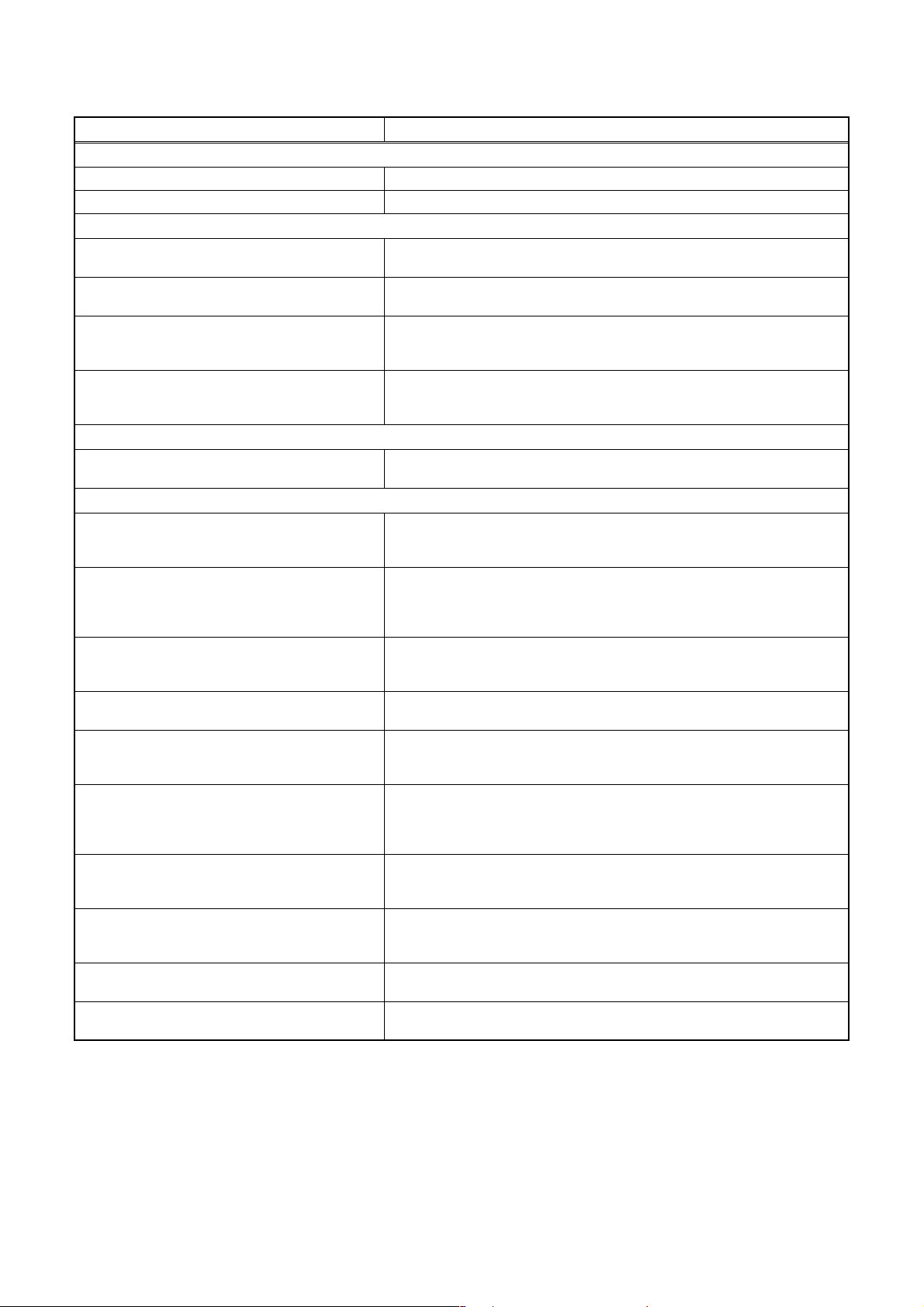
LASER BEAM SAFETY PRECAUTIONS
This DVD player uses a pickup that emits a laser beam.
Do not look directly at the laser beam coming
from the pickup or allow it to strike against your
skin.
The laser beam is emitted from the location shown in the figure. When checking the laser diode, be sure to keep
your eyes at least 30 cm away from the pickup lens when the diode is turned on. Do not look directly at the laser
beam.
CAUTION: Use of controls and adjustments, or doing procedures other than those specified herein, may result in
hazardous radiation exposure.
Drive Mechanism Assembly
Laser Beam Radiation
Laser Pickup
Turntable
Location: Inside Top of DVD mechanism.
1-2-1 R4PLSP
Page 5

IMPORTANT SAFETY PRECAUTIONS
Product Safety Notice
Some electrical and mechanical parts have special
safety-related characteristics which are often not evident from visual inspection, nor can the protection
they give necessarily be obtained by replacing them
with components rated for higher voltage, wattage,
etc. Parts that have special safety characteristics are
identified by a ! on schematics and in parts lists. Use
of a substitute replacement that does not have the
same safety characteristics as the recommended
replacement part might create shock, fire, and/or other
hazards. The Product’s Safety is under review continuously and new instructions are issued whenever
appropriate. Prior to shipment from the factory, our
products are carefully inspected to confirm with the
recognized product safety and electrical codes of the
countries in which they are to be sold. However, in
order to maintain such compliance, it is equally important to implement the following precautions when a set
is being serviced.
Precautions during Servicing
A. Parts identified by the ! symbol are critical for
safety. Replace only with part number specified.
B. In addition to safety, other parts and assemblies
are specified for conformance with regulations
applying to spurious radiation. These must also be
replaced only with specified replacements.
Examples: RF converters, RF cables, noise blocking capacitors, and noise blocking filters, etc.
C. Use specified internal wiring. Note especially:
1)Wires covered with PVC tubing
2)Double insulated wires
3)High voltage leads
D. Use specified insulating materials for hazardous
live parts. Note especially:
1)Insulation tape
2)PVC tubing
3)Spacers
4)Insulators for transistors
E. When replacing AC primary side components
(transformers, power cord, etc.), wrap ends of
wires securely about the terminals before soldering.
F. Observe that the wires do not contact heat produc-
ing parts (heatsinks, oxide metal film resistors, fusible resistors, etc.).
G. Check that replaced wires do not contact sharp
edges or pointed parts.
H. When a power cord has been replaced, check that
5 - 6 kg of force in any direction will not loosen it.
I. Also check areas surrounding repaired locations.
J. Be careful that foreign objects (screws, solder
droplets, etc.) do not remain inside the set.
K. When connecting or disconnecting the internal
connectors, first, disconnect the AC plug from the
AC outlet.
1-3-1 DVD_SFNP
Page 6
Safety Check after Servicing
Examine the area surrounding the repaired location
for damage or deterioration. Observe that screws,
parts, and wires have been returned to their original
positions. Afterwards, do the following tests and confirm the specified values to verify compliance with
safety standards.
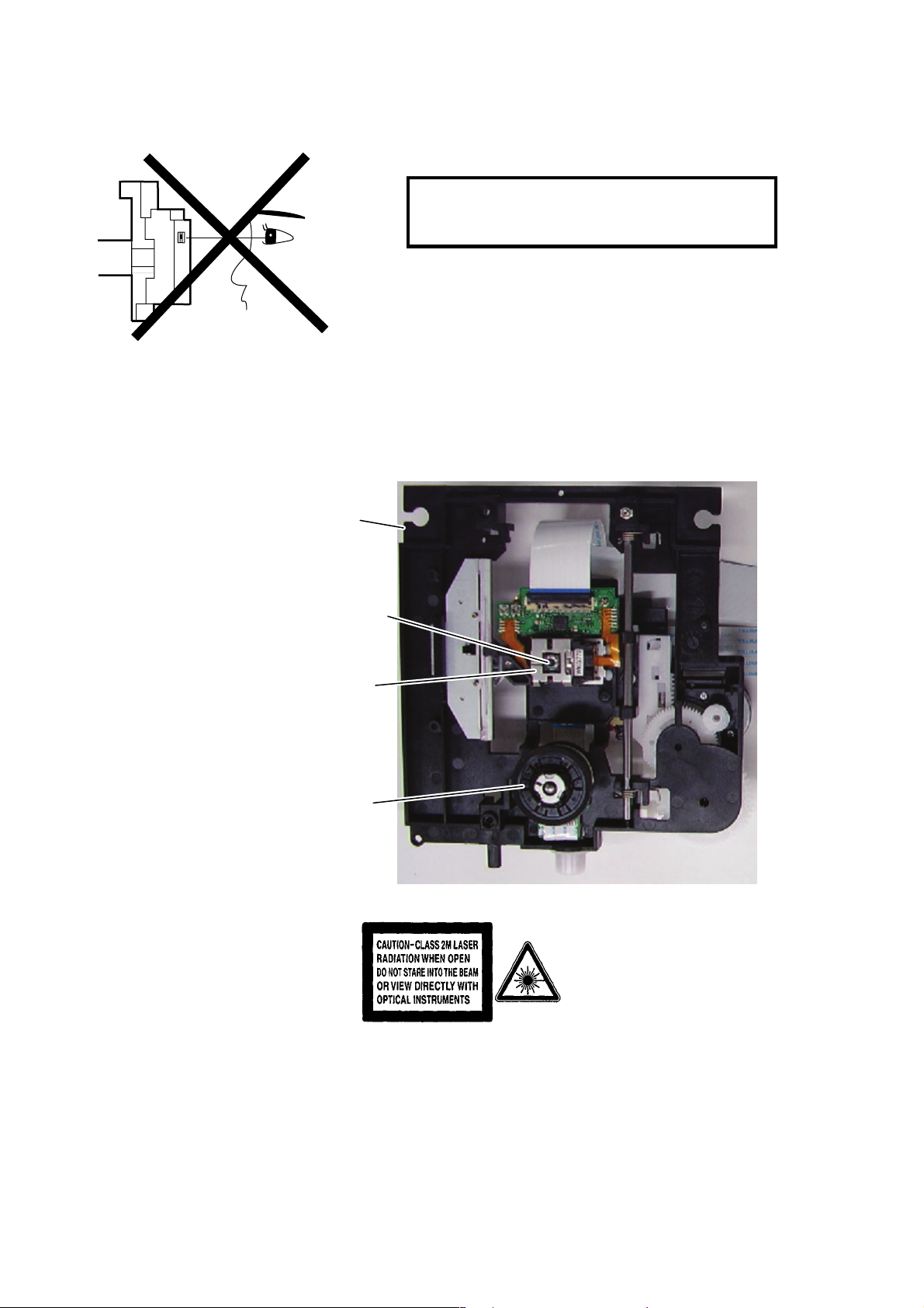
1. Clearance Distance
When replacing primary circuit components, confirm
specified clearance distance (d) and (d’) between soldered terminals, and between terminals and surrounding metallic parts. (See Fig. 1)
Table 1 : Ratings for selected area
AC Line Voltage Clearance Distance (d), (d’)
220 to 240 V
Note: This table is unofficial and for reference only.
Be sure to confirm the precise values.
2. Leakage Current Test
≥ 3 mm(d)
≥ 6 mm(d’)
Chassis or Secondary Conductor
Primary Circuit
d' d
Fig. 1
Exposed Accessible Part
Confirm the specified (or lower) leakage current
between B (earth ground, power cord plug prongs)
and externally exposed accessible parts (RF terminals, antenna terminals, video and audio input and
output terminals, microphone jacks, earphone jacks,
etc.) is lower than or equal to the specified value in the
table below.
Measuring Method (Power ON) :
Insert load Z between B (earth ground, power cord
plug prongs) and exposed accessible parts. Use an
AC voltmeter to measure across the terminals of load
Z. See Fig. 2 and the following table.
Table 2: Leakage current ratings for selected areas
AC Line Voltage Load Z Leakage Current (i)
220 to 240 V
2kΩ RES.
Connected in
parallel
50kΩ RES.
Connected in
parallel
i≤0.7mA AC Peak
i≤2mA DC
i≤0.7mA AC Peak
i≤2mA DC
Z
One side of
B
Power Cord Plug Prongs
One side of power cord plug
AC Voltmeter
(High Impedance)
prongs (B) to:
RF or
Antenna terminals
A/V Input, Output
Fig. 2
Note: This table is unofficial and for reference only. Be sure to confirm the precise values.
1-3-2 DVD_SFNP
Page 7
STANDARD NOTES FOR SERVICING
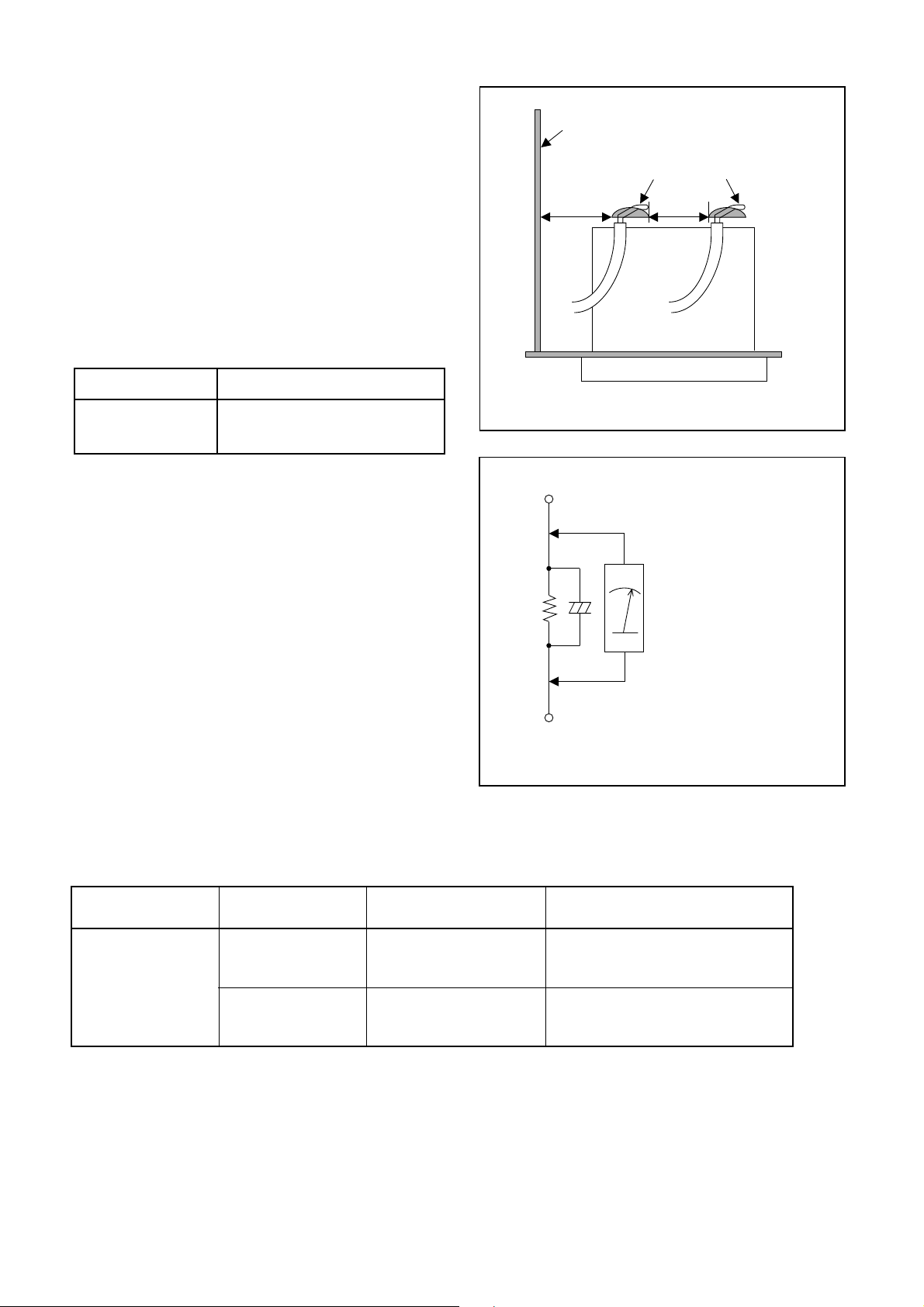
Circuit Board Indications
1. The output pin of the 3 pin Regulator ICs is
indicated as shown.
Top View
Out
2. For other ICs, pin 1 and every fifth pin are
indicated as shown.
Pin 1
3. The 1st pin of every male connector is indicated as
shown.
Pin 1
Input
In
Bottom View
5
10
Pb (Lead) Free Solder
When soldering, be sure to use the Pb free solder.
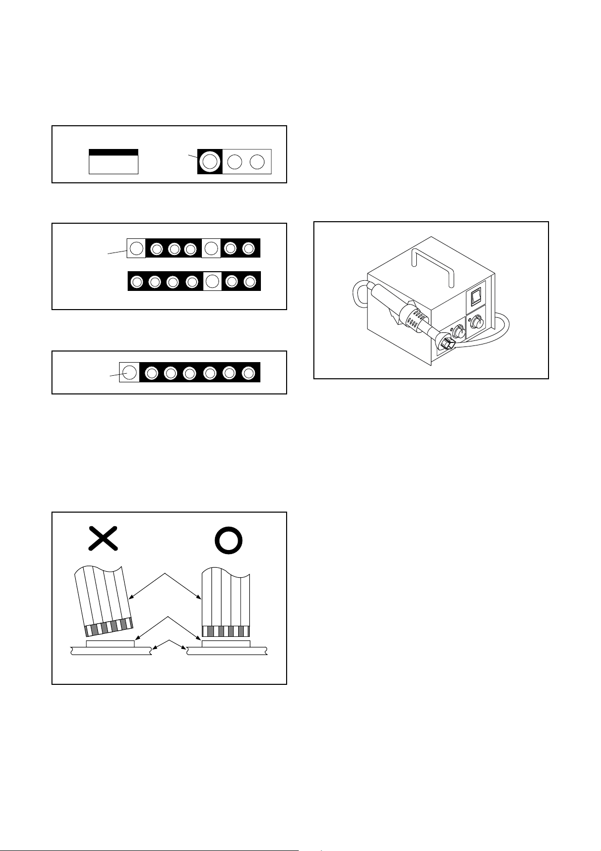
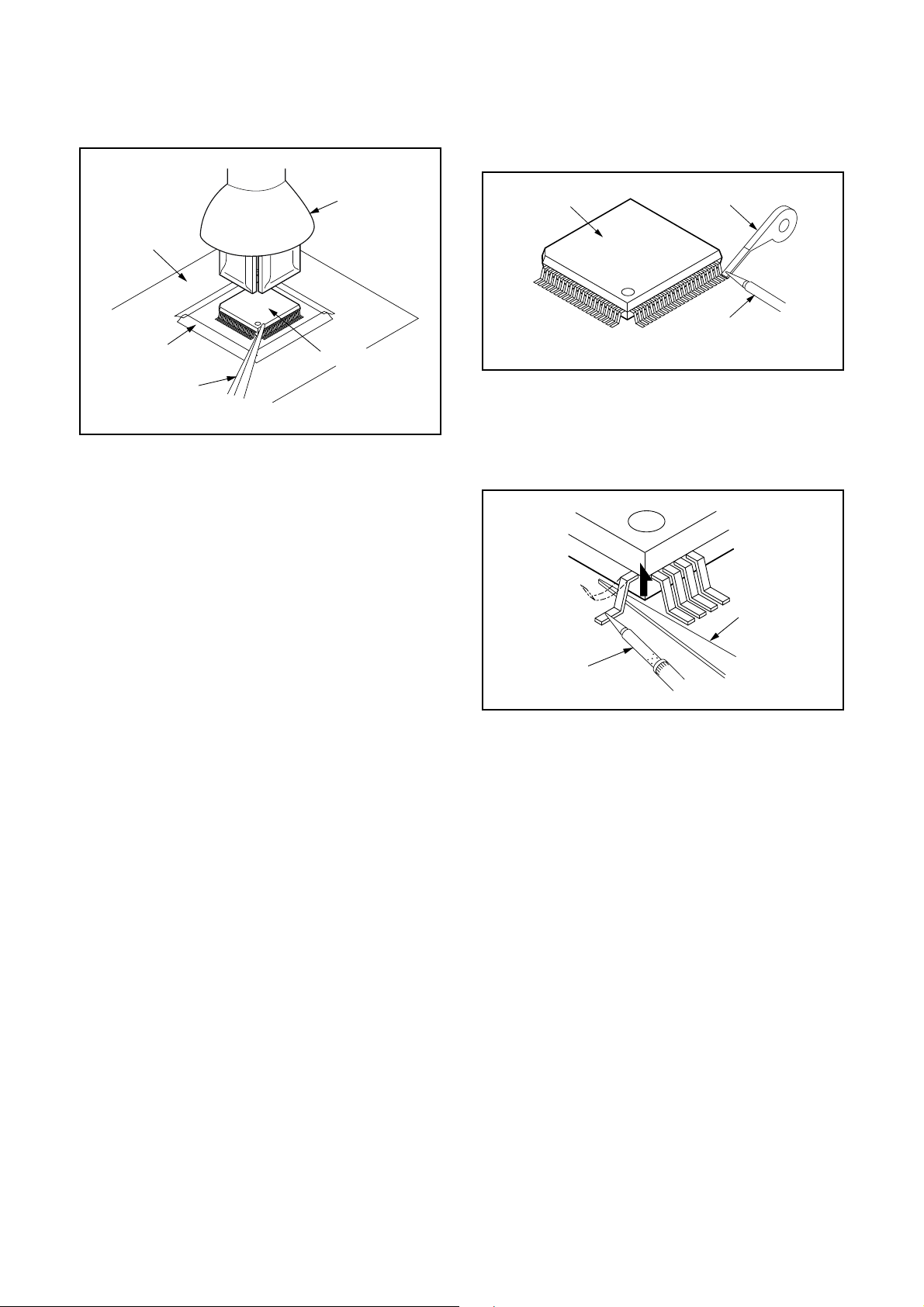
How to Remove / Install Flat Pack-IC
1. Removal
With Hot-Air Flat Pack-IC Desoldering Machine:
1. Prepare the hot-air flat pack-IC desoldering
machine, then apply hot air to the Flat Pack-IC
(about 5 to 6 seconds). (Fig. S-1-1)
Fig. S-1-1
Instructions for Connectors
1. When you connect or disconnect the FFC (Flexible
Foil Connector) cable, be sure to first disconnect
the AC cord.
2. FFC (Flexible Foil Connector) cable should be
inserted parallel into the connector, not at an
angle.
FFC Cable
Connector
CBA
* Be careful to avoid a short circuit.
2. Remove the flat pack-IC with tweezers while
applying the hot air.
3. Bottom of the flat pack-IC is fixed with glue to the
CBA; when removing entire flat pack-IC, first apply
soldering iron to center of the flat pack-IC and heat
up. Then remove (glue will be melted). (Fig. S-1-6)
4. Release the flat pack-IC from the CBA using
tweezers. (Fig. S-1-6)
CAUTION:
1. The Flat Pack-IC shape may differ by models. Use
an appropriate hot-air flat pack-IC desoldering
machine, whose shape matches that of the Flat
Pack-IC.
2. Do not supply hot air to the chip parts around the
flat pack-IC for over 6 seconds because damage
to the chip parts may occur. Put masking tape
around the flat pack-IC to protect other parts from
damage. (Fig. S-1-2)
1-4-1 DVDP_SN
Page 8
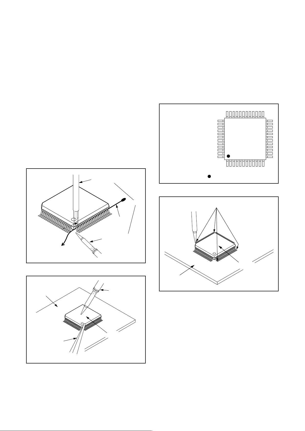
3. The flat pack-IC on the CBA is affixed with glue, so
be careful not to break or damage the foil of each
pin or the solder lands under the IC when
removing it.
With Soldering Iron:
1. Using desoldering braid, remove the solder from
all pins of the flat pack-IC. When you use solder
flux which is applied to all pins of the flat pack-IC,
you can remove it easily. (Fig. S-1-3)
CBA
Masking
Tape
Tweezers
Hot-air
Flat Pack-IC
Desoldering
Machine
Flat Pack-IC
Fig. S-1-2
Flat Pack-IC
Desoldering Braid
Soldering Iron
Fig. S-1-3
2. Lift each lead of the flat pack-IC upward one by
one, using a sharp pin or wire to which solder will
not adhere (iron wire). When heating the pins, use
a fine tip soldering iron or a hot air desoldering
machine. (Fig. S-1-4)
Sharp
Pin
Fine Tip
Soldering Iron
3. Bottom of the flat pack-IC is fixed with glue to the
CBA; when removing entire flat pack-IC, first apply
soldering iron to center of the flat pack-IC and heat
up. Then remove (glue will be melted). (Fig. S-1-6)
4. Release the flat pack-IC from the CBA using
tweezers. (Fig. S-1-6)
Fig. S-1-4
1-4-2 DVDP_SN
Page 9
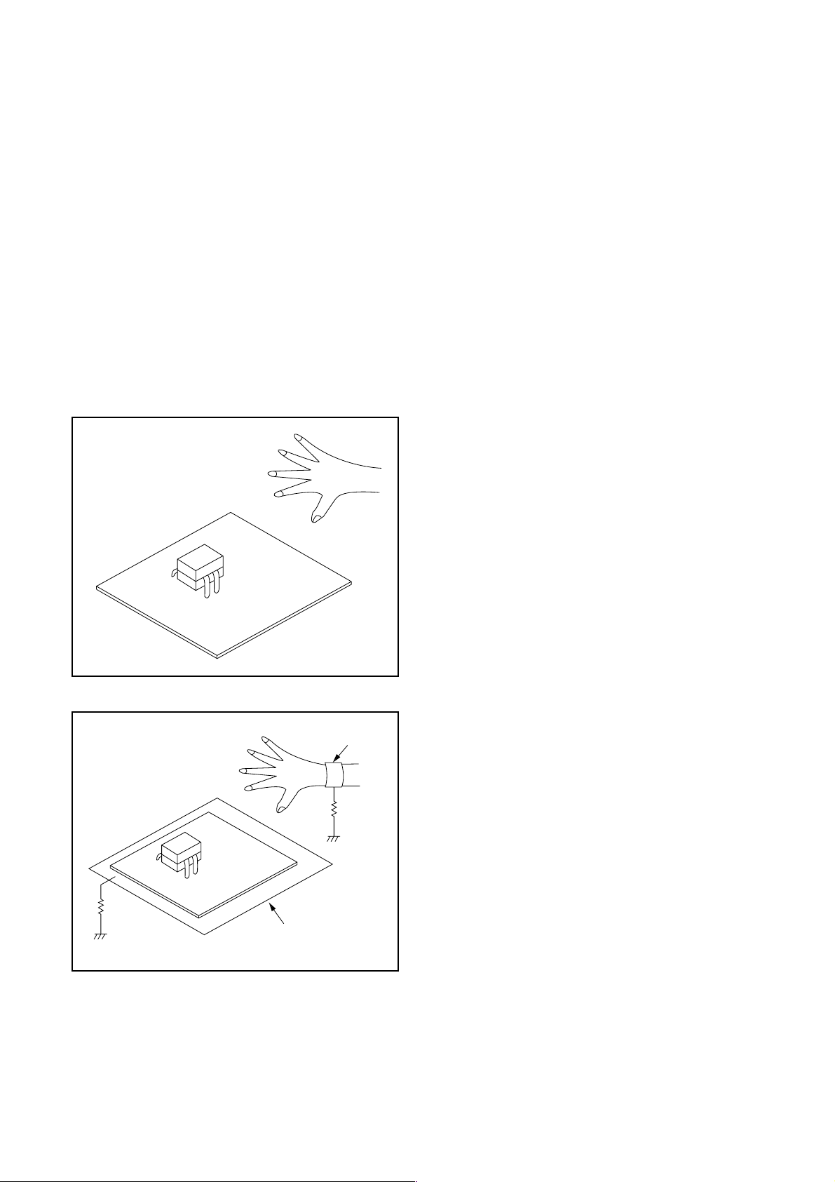
With Iron Wire:
1. Using desoldering braid, remove the solder from
all pins of the flat pack-IC. When you use solder
flux which is applied to all pins of the flat pack-IC,
you can remove it easily. (Fig. S-1-3)
2. Affix the wire to a workbench or solid mounting
point, as shown in Fig. S-1-5.
3. While heating the pins using a fine tip soldering
iron or hot air blower, pull up the wire as the solder
melts so as to lift the IC leads from the CBA
contact pads as shown in Fig. S-1-5.
4. Bottom of the flat pack-IC is fixed with glue to the
CBA; when removing entire flat pack-IC, first apply
soldering iron to center of the flat pack-IC and heat
up. Then remove (glue will be melted). (Fig. S-1-6)
5. Release the flat pack-IC from the CBA using
tweezers. (Fig. S-1-6)
Note: When using a soldering iron, care must be
taken to ensure that the flat pack-IC is not
being held by glue. When the flat pack-IC is
removed from the CBA, handle it gently
because it may be damaged if force is applied.
Hot Air Blower
2. Installation
1. Using desoldering braid, remove the solder from
the foil of each pin of the flat pack-IC on the CBA
so you can install a replacement flat pack-IC more
easily.
2. The “●” mark on the flat pack-IC indicates pin 1.
(See Fig. S-1-7.) Be sure this mark matches the 1
on the PCB when positioning for installation. Then
presolder the four corners of the flat pack-IC. (See
Fig. S-1-8.)
3. Solder all pins of the flat pack-IC. Be sure that
none of the pins have solder bridges.
Example :
Pin 1 of the Flat Pack-IC
is indicated by a " " mark.
Fig. S-1-7
To Solid
Mounting Point
CBA
Tweezers
Iron Wire
Soldering Iron
Fig. S-1-5
Fine Tip
Soldering Iron
Flat Pack-IC
or
Presolder
Flat Pack-IC
CBA
Fig. S-1-8
Fig. S-1-6
1-4-3 DVDP_SN
Page 10
Instructions for Handling Semiconductors
Electrostatic breakdown of the semi-conductors may
occur due to a potential difference caused by
electrostatic charge during unpacking or repair work.
1. Ground for Human Body
Be sure to wear a grounding band (1 MΩ) that is
properly grounded to remove any static electricity that
may be charged on the body.
2. Ground for Workbench
Be sure to place a conductive sheet or copper plate
with proper grounding (1 MΩ) on the workbench or
other surface, where the semi-conductors are to be
placed. Because the static electricity charge on
clothing will not escape through the body grounding
band, be careful to avoid contacting semi-conductors
with your clothing.
<Incorrect>
<Correct>
1MΩ
CBA
Grounding Band
1MΩ
CBA
Conductive Sheet or
Copper Plate
1-4-4 DVDP_SN
Page 11
HANDLING PRECAUTIONS FOR HDD
CAUTION:
1. SHOCK
a. Exposing HDD to shock may be the biggest
damaging factor. Please note that HDD is easily
damaged even if dropped from any height. Be sure
to place HDD on a shock-absorbent mat. Also, be
careful when transporting HDD.
b. Be careful not to subject HDD to any shock when
tightening screws for HDD replacement.
(Tighten screws manually, not with an electric
driver.)
2. MOISTURE
a. Moisture may also be a damaging factor. HDD is
semiclosed style. Sudden changes in ambient
temperature may cause moisture to form. Monitor
temperature and do not allow moisture to form on
the media surface. Also, when opening HDD
package, do so only after package is at ambient
temperature.
b. After replacing HDD, leave it to reach room
temperature (about 2 hours) for preventing dew
internal condensation, and then work necessary
task such as operation check.
4. OTHERS
a. Be careful so as not to do the followings.
Otherwise, HDD might be damaged.
- DO NOT disassemble HDD.
- When handling HDD, be sure to hold both sides
securely.
b. HDD should be stored, packed in the protective
bag, in suitable surroundings (i.e., no extreme
changes in temperature to avoid condensation).
c. When transporting HDD, be sure to use the
exclusive packing case (the replacement HDD
carton).
d. Do not stack HDDs.
e. Do not place vertically because HDD is unstable
and easy to fall.
3. STATIC ELECTRICITY
a. After removing HDD or taking replacement HDD
out of the protective bag (the replacement HDD is
packed in a protective bag), place HDD on a
conductive surface. A grounding band should be
worn when handling.
Grounding Band
Both the conductive surface and grounding band
should be grounded.
b. Make sure that HDD is placed on main unit
completely and then let go of it, when assembling.
c. Do not put HDD on a packing bag. (for preventing
electrostatic damage)
1-5-1 DHD_SN
Page 12
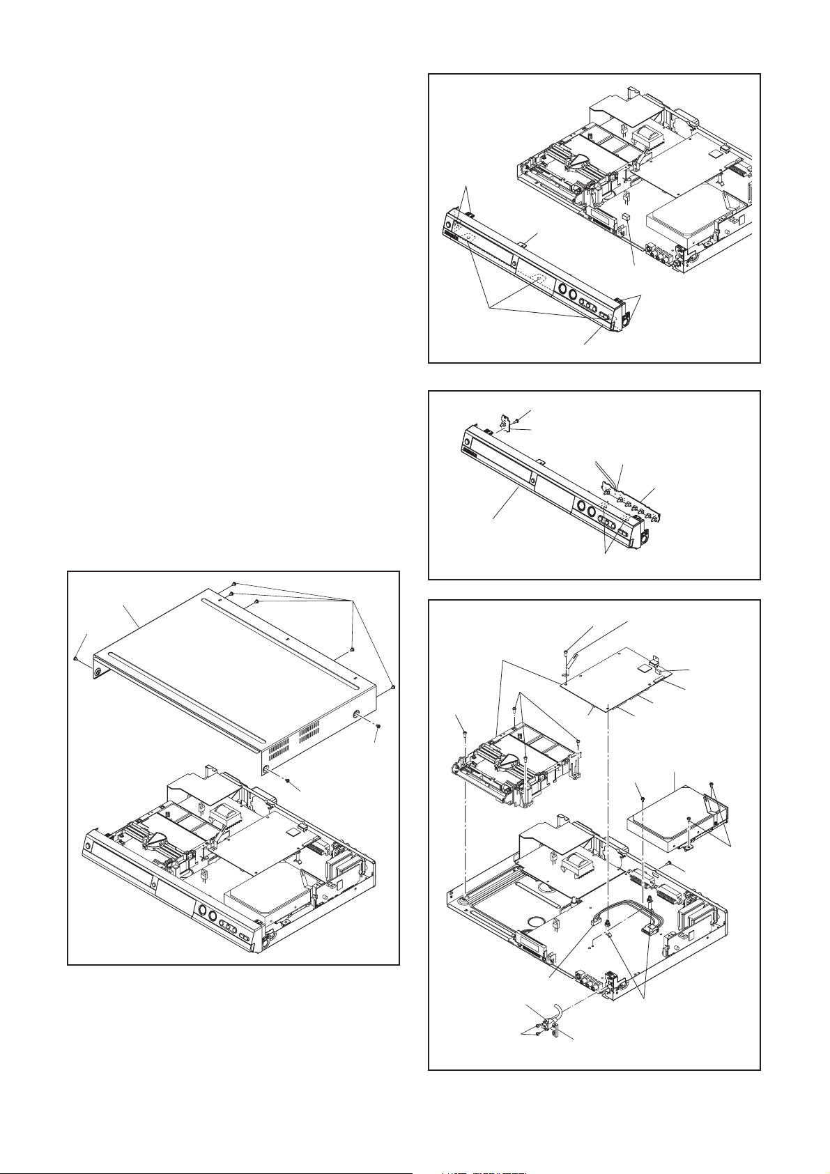
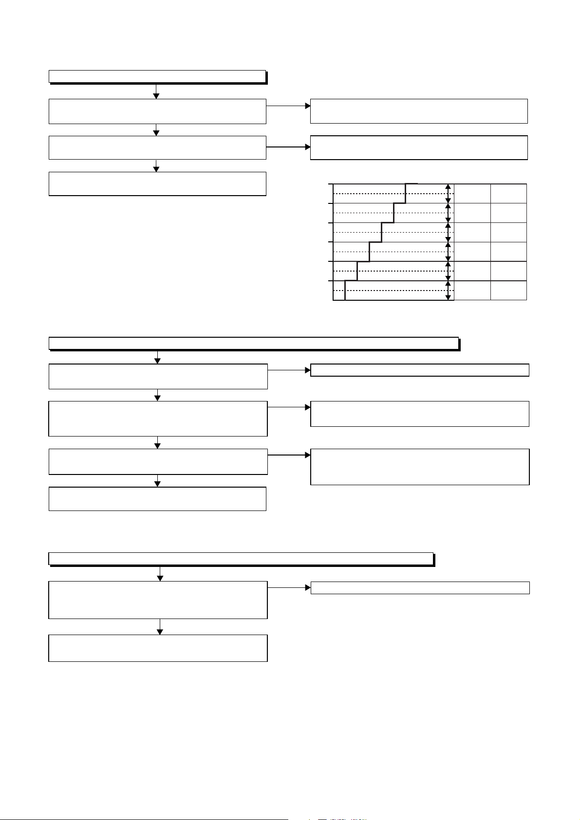
CABINET DISASSEMBLY INSTRUCTIONS
1. Disassembly Flowchart
This flowchart indicates the disassembly steps to gain
access to item(s) to be serviced. When reassembling,
follow the steps in reverse order. Bend, route, and
dress the cables as they were originally.
[1] Top Cover
[3] SW CBA
[4] Power SW
CBA
[8] IEEE 1394
DV-IN Cable
[12] Fan Cover
[13] Motor DC Fan
[14] Rear Panel
[2] Front Unit
[5] Front Assembly
[7] DVD Mechanism
& DVD/HDD Main
CBA Assembly
[15] Power
Supply CBA
[16] AV CBA
[17] DTV Module
Assembly
[18] Main PCB
Holder
[19] Front
Bracket R
[6] HDD Assembly
[9] ATA CBA
[10] HDD Bracket
[11] Hard Disk Drive
2. Disassembly Method
ID/
LOC.
No.
PART
Fig.
No.
[1] Top Cover D1 8(S-1) ---
[2] Front Unit D2
[3] SW CBA D3 *CN1063, *2(L-3) 1-3
Power SW
[4]
[5]
[6]
CBA
Front
Assembly
HDD
Assembly
D3 (S-2) ---
D3 ---------- ---
D4
DVD
Mechanism
[7]
&
DVD/HDD
D4
Main CBA
Assembly
REMOVAL
REMOVE/*UNHOOK/
UNLOCK/RELEASE/
UNPLUG/DESOLDER
*CN1651, *5(L-1),
*3(L-2)
*CN1015, *CN651,
3(S-3)
(S-4), 4(S-5), (S-6),
*CN101, *CN503,
*CN701, *CN901,
PCB Support / PCB
Spacers,
M-PCB Plate Earth
Note
1
1-1
1-2
---
2
ID/
LOC.
No.
[10]
[11]
PAR T
HDD
Bracket
Hard Disk
Drive
REMOVE/*UNHOOK/
Fig.
UNLOCK/RELEASE/
No.
UNPLUG/DESOLDER
Note
D5 4(S-8) ---
(S-9), HDD Earth
D5
Plate
3-1
3-2
3-3
[12] Fan Cover D6 2(S-10) ---
REMOVAL
Motor DC
[13]
Fan
[14] Rear Panel D6
Power
[15]
Supply
CBA
D6 Fan Earth ---
*CN1601, (S-11),
2(S-12), 2(S-13)
*CN1152, 4(S-14),
D7
Power Holder
---
---
[16] AV CBA D7 5(S-15) ---
[17]
[18]
[19]
↓
(1)
DTV
Module
Assembly
Main PCB
Holder
Front
Bracket R
↓
(2)
Desolder,
D7
Module PCB Holder
---
D7 (S-16) ---
D7 (S-17) ---
↓
(3)
↓
(4)
(5)
Note:
(1): Identification (location) No. of parts in the figures
(2): Name of the part
(3): Figure Number for reference
(4): Identification of parts to be removed, unhooked,
unlocked, released, unplugged, unclamped, or
desoldered.
P=Spring, L=Locking Tab, S=Screw,
CN=Connector
*=Unhook, Unlock, Release, Unplug, or Desolder
e.g. 7(S-1) = seven Screws (S-1),
5(L-1) = five Locking Tabs (L-1)
(5): Refer to “Reference Notes.”
3
↓
IEEE 1394
[8]
DV-IN
D4 2(S-7), DV Earth Plate ---
Cable
[9] ATA CBA D5 *CN3001 ---
1-6-1 E2J00DC
Page 13
Reference Notes
1. Locking Tabs (L-1) ,(L-2) and (L-3) are fragile. Be
careful not to break them.
1-1. Release five Locking Tabs (L-1).
1-2. Release three Locking Tabs (L-2) and
remove the Front Unit.
1-3. Release two Locking Tabs (L-3) and remove
the SW CBA.
2. The DVD Mechanism & DVD/HDD Main CBA
Assembly is adjusted as a unit at factory.
Therefore, do not disassemble it.
Replace the DVD Mechanism & DVD/HDD Main
CBA Assembly as a unit.
3. Whenever you have replaced the Hard Disk Drive,
initialize the Hard Disk Drive. To initialize the Hard
Disk Drive, perform the following.
3-1. To put the HDD & DVD Recorder into the
HDD mode, press the [HDD] button on the
remote control unit.
3-2. To put the HDD & DVD Recorder into the self-
check mode, after pressing [VARIABLE
SKIP] button, press the [0], [7], and [9]
buttons on the remote control unit in that
order within three seconds.
3-3. Press [ENTER/OK] button. The HDD & DVD
Recorder is initialized and the power is
turned off automatically after two seconds.
(L-1)
(L-1)
(L-2)
[2] Front Unit
(S-2)
[4] Power SW CBA
[5] Front Assembly
CN1651
(L-1)
Fig. D2
CN1063
[3] SW CBA
[1] Top Cover
(S-1)
(S-1)
(S-1)
(S-1)
Fig. D1
[7]
DVD Mechanism
*
& DVD/HDD Main
CBA Assembly
(S-5)
(S-5)
(L-3)
(S-4)
CN901
Fig. D3
M-PCB Plate
Earth
CN503
CN651
CN101
CN701
[6] HDD
Assembly
(S-3)
(S-3)
(S-6)
CN1015
[8] IEEE 1394
DV-IN Cable
(S-7)
See Reference Notes 2.
*
DV Earth Plate
PCB Support /
PCB Spacers
Fig. D4
1-6-2 E2J00DC
Page 14
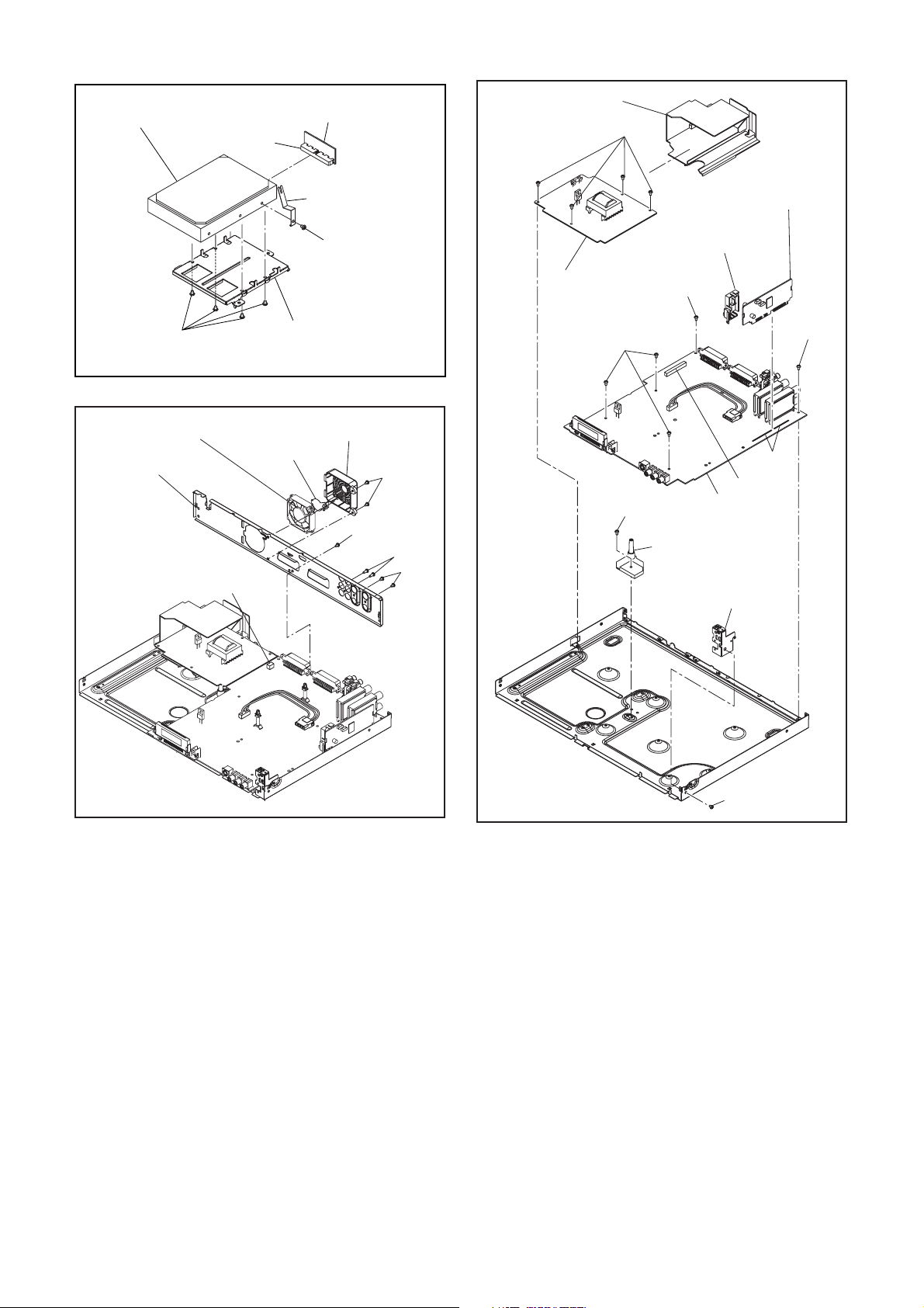
[11] Hard Disk Drive
CN3001
[9] ATA CBA
Power Holder
(S-14)
(S-8)
[13] Motor DC Fan
[14] Rear Panel
CN1601
HDD Earth Plate
(S-9)
[10] HDD Bracket
[12] Fan Cover
Fan Ea r th
(S-11)
Fig. D5
(S-10)
(S-12)
(S-13)
[15] Power
Supply CBA
(S-15)
(S-16)
[17] DTV Module
Assembly
Module PCB
Holder
(S-15)
(S-15)
Desolder
CN1152
[16] AV CBA
[18] Main PCB
Holder
[19] Front
Bracket R
Fig. D6
(S-17)
Fig. D7
1-6-3 E2J00DC
Page 15
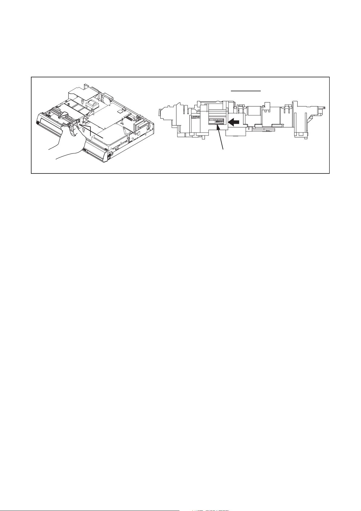
3. How to Eject Manually
Note: When rotating the gear, be careful not to damage the gear.
1. Remove the Top Cover.
2. Rotate the gear in the direction of the arrow manually as shown below until the tray descends.
3. Pull the tray out manually and remove a disc.
View for A
A
Rotate this gear in
the direction of the arrow
1-6-4 E2J00DC
Page 16
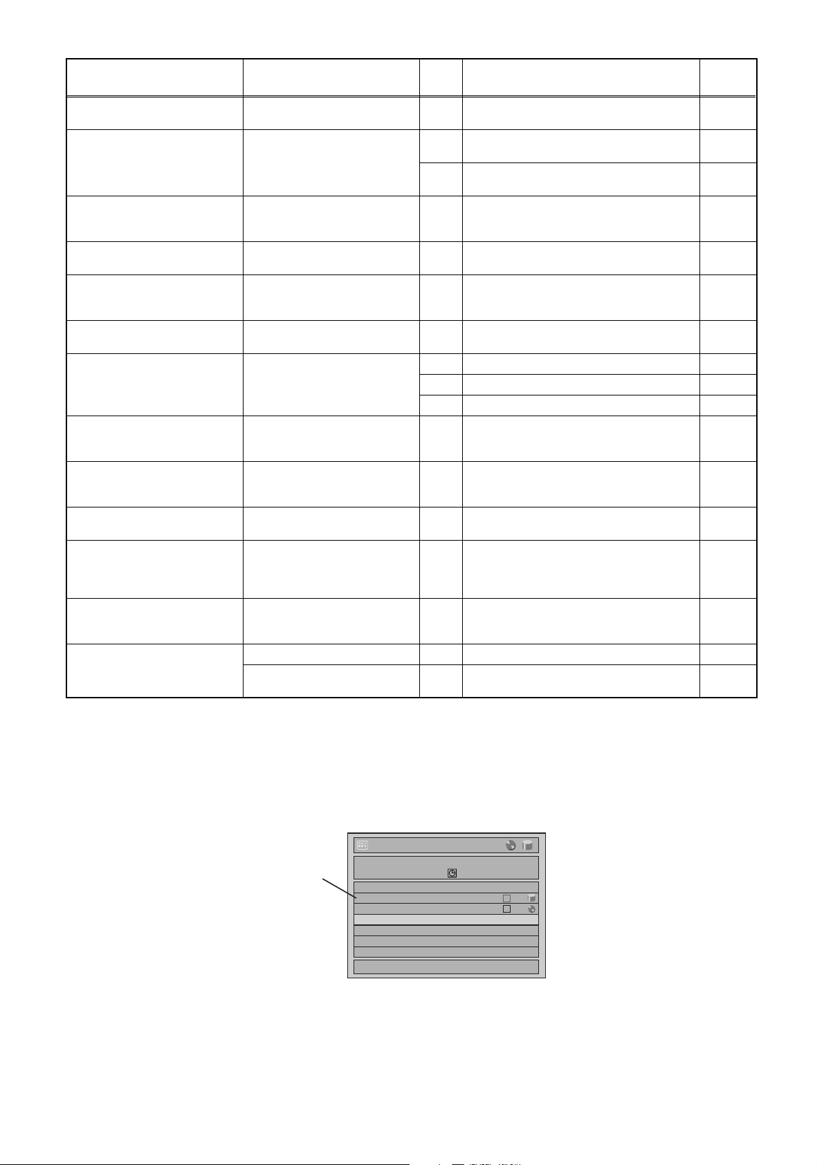
HOW TO SELF-CHECK AND INITIALIZE THE HDD & DVD RECORDER
1. Turn on the HDD & DVD Recorder.
2. To put the HDD & DVD Recorder into the HDD mode, press [HDD] on the remote control unit.
3. To put the HDD & DVD Recorder into the self-check mode, after pressing [VARIABLE SKIP] button, press the
[0], [7], and [9] buttons on the remote control unit in that order within three seconds.
Fig. a appears on the screen and all LEDs light.
SELF CHECK
*1
*2
DVD CONNECT STATUS : --
HDD CONNECT STATUS : --
*3
HDD POWER ON HOURS :
POWER OFF : POWER
Fig. a: Self-Check Mode Screen
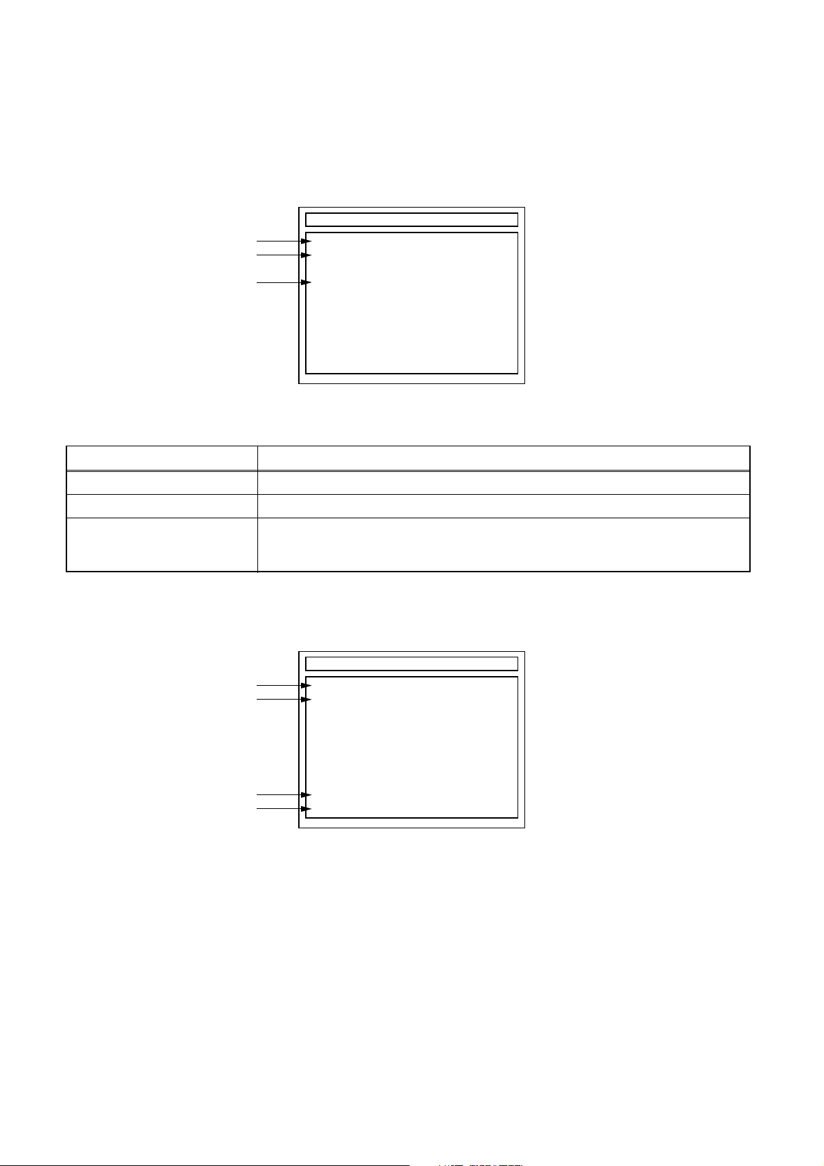
Table 1: Description of Fig. a
INDICATION DESCRIPTION
DVD CONNECT STATUS (*1) Connecting Condition of DVD(F/E)
HDD CONNECT STATUS (*2) Connecting Condition of HDD
Value of HDD power on hours obtained from S.M.A.R.T. command. (If not obtainable,
HDD POWER ON HOURS (*3)
value of HDD power on hours is “0”.)
Value in parentheses is the factory setting value. (If no setting, the value is “0”.)
4. Upon the self-check completion, Fig. b appears on the screen.
SELF CHECK
*4
*5
DVD CONNECT STATUS : OK
HDD CONNECT STATUS : OK
HDD POWER ON HOURS : 120
*6
*7
HDD FORMAT : ENTER
POWER OFF : POWER
Fig. b: Screen of Finishing Self-Check Mode
1-7-1 E2J00INT
Page 17
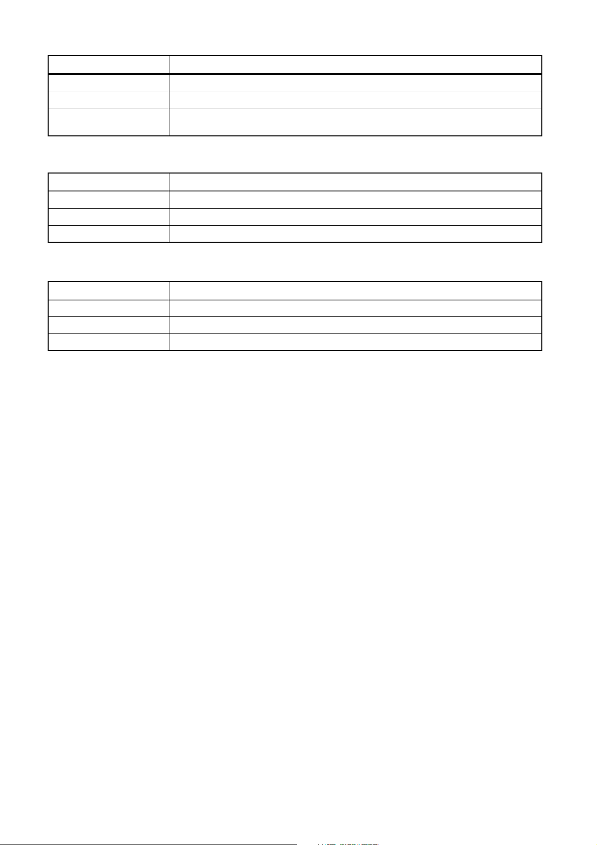
Table 2: Indication of DVD self-check (*4)
INDICATION DESCRIPTION
OK Connection of DVD is normal.
NOT FOUND DVD drive cannot be found.
CABLE ERROR
FFC cable (connecting to CN401) between the DVD drive and the DVD/HDD MAIN CBA is
not connected correctly.
Table 3: Indication of HDD self-check (*5)
INDICATION DESCRIPTION
OK Connection of HDD is normal.
NOT FOUND HDD drive cannot be found.
CABLE ERROR FFC cable between the ATA CBA and the HDD drive is not connected correctly.
Table 4: Available button in self-check mode
BUTTON DESCRIPTION
ENTER/OK (*6) Initialize (only when the self-check mode is complete)
STANDBY-ON (*7) Turn the power off (when the self-check mode is complete)
OTHER Not available
5. When the self-check mode is complete, press [STANDBY-ON] button to turn the power off.
When initializing the HDD & DVD recorder, press [ENTER/OK] button. After two seconds, the power is turned
off automatically.
NOTE: When initializing, “Current Clock”, “Setup Changing Item”, “Channel Setup”, “Area Setup”, “Program” and
“HDD Contents” are initialized.
1-7-2 E2J00INT
Page 18
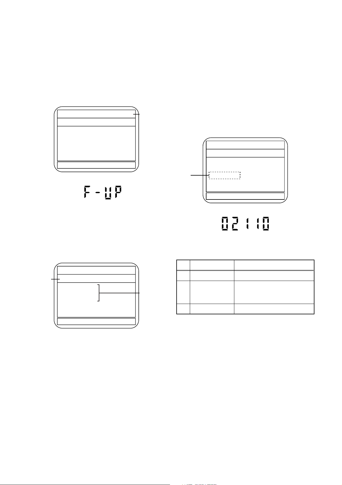
FIRMWARE RENEWAL MODE
e
1. Turn the power on and remove the disc on the tray.
2. To put the HDD & DVD recorder into version up
mode, press [VARIABLE SKIP], [6], [5], and [4]
buttons on the remote control unit in the order.
Then the tray will open automatically.
Fig. a appears on the screen and Fig. b appears
on the VFD.
* Firmware Version differs depending on the
models, and this indication is one example.
Firm Update Mode
Please insert a disc.
ver. HD4A*****H1E
Current
F/W version
is displayed.
Fig. a Version Up Mode Screen
Fig. b VFD in Version Up Mode
3. Load the disc for version up.
Fig. c appears on the screen. The file on the top is
highlighted as the default.
When there is only one file to exist, Step 4 will
start automatically.
* Firmware Version differs depending on the
models, and this indication is one example.
Firm Update Mode ver. HD4A*****H1E
Disc name
is displayed.
VOL_200703250934
1 HD4A10210H1E
2 HD4A10211H1E
3 HD4A10212H1E
4 HD4A10213H1E
Files included
in the disc ar
displayed.
4. Select the firmware version pressing arrow
buttons, then press [ENTER/OK].
Fig. d appears on the screen and Fig. e appears
on the VFD. The HDD & DVD recorder starts
updating.
About VFD indication of Fig. e:
1) When Fig. d is displayed on the screen, “F-UP”
is displayed on the VFD.
2) When “Firmware Updating... XX% Complete.”
is displayed on the screen, “02110” is displayed
on the VFD.
* Firmware Version differs depending on the
models, and this indication is one example.
Firm Update Mode ver. HD4A*****H1E
Firm Update Mode
(*1)
File Loading...
Fig. d Programming Mode Screen
Fig. e VFD in Programming Mode (Example)
The appearance shown in (*1) of Fig. d is
described as follows.
No. Appearance State
1 File Loading... Sending files into the memory
Firmware
2
Updating...
Writing new version data
XX% Complete.
--- Error Failed in updating
1 / 1
Fig. c Update Disc Screen
5. After updating is finished, the tray opens
automatically.
At this time, no button is available.
6. Pull out the AC code once, then insert it again.
1-8-1 E2J00FW
Page 19
FUNCTION INDICATOR SYMBOLS
Note: If an error occurs, a message with the error number appears on the screen.
Recording Error
Message Solution
Can not record on this disc.
This program is not allowed to
be recorded.
This program is not recordable
in Video mode.
This program is not allowed to
be recorded on this disc.
This disc is protected and not
recordable.
You cannot record on this disc as
Power Calibration Area is full.
Insert a recordable disc, and
ensure the disc status satisfies
the recording requirements.
You cannot record copyprohibited programs.
You cannot record copyprohibited programs.
You cannot record cop-y
prohibited programs.
Release the disc protection
setting in the Disc Setting
menu.
Error message
E35
Error
No.
1 An error occurs during data reading. -
2
3
4 An error occurs with OPC. -
5 During recovery in a record. -
6
7 An error occurs in a format. -
8 It cannot start an encode. -
9
10
11
12
13 It is a reply that “ATAPI is not readable.” -
14
15
16 An error occurs in Finalize Close. -
17 An error occurs in Rec Stop Close. -
18 An error occurs in PCA Full (DVD_R). -
19 Safety Stop occurs during editing. -
20 High Speed Disc. 2
21 The disc is not formatted. 5
22 Disc Error has occurred. 3
24
25 During the Macrovision picture input. 11
26 During the CGMS picture input. 12
27
28
29 Disc Protected Disc. 6
Error No.
Error Description Priority
There is no reply for 15 seconds in Test
Unit Ready.
Cannot write the data after trying three
times.
An error occurs even if recovery has been
tried three times.
NV_PCK/RDI_PCK is not in encoded
data.
Encode Pause condition continued for 10
minutes.
Encode Pause condition continued in
normal REC condition for 10 minutes.
Difference in the address and cannot get
Stream ID of RDI/VIDEO.
Cannot write the data after recovering
SMALL VMGI.
Cannot write the data after DVD-R
Reverse Track.
The disc except DVD-R/RW or finalized
DVD-R.
During the CGMS picture input. (Video
Format Disc)
During the CGMS picture input. (VR
Format Disc)
-
-
-
-
-
-
-
-
-
1
-
-
1-9-1 E2J00FIS
Page 20
Message Solution
Disc is full.
(No area for new recording)
You cannot record more than
99 titles on one disc. (The
maximum is 99.)
You cannot record more than
999 chapters on one disc.
(The maximum is 999.)
You cannot record on this as
Control Information is full.
You cannot record on this disc
as Power Calibration Area is
full.
This disc is already finalized.
Can not record on this disc. Repeat the same operation.
You cannot record more than
49 titles on the disc. (The
maximum is 49.)
You cannot record more than
254 chapters on the disc. (The
maximum is 254.)
This program is not recordable
in +VR mode.
The disc has no recording
compatibility. Set “Make
Recording Compatible” to
“ON” to convert the disc.
You cannot record more than
600 titles on HDD. (The
maximum is 600.)
Can not record on this HDD.
Insert a recordable disc with
enough recording space.
Delete unnecessary titles.
Delete unnecessary chapters. 33
Insert a new disc. 34
Insert a new disc. 35 PCA is Full. (in REC start) 4
Release the finalizing for this
disc.
Delete unnecessary titles. 43
Delete unnecessary chapter
marks.
You cannot record copyprohibited programs.
Set “Make Recording
Compatible” to “ON” to convert
the disc.
Delete unnecessary titles. 47
Connect HDD. 48 Recording without HDD connected. -
Delete unnecessary
programs.
Error
No.
Error Description Priority
30 No available recording space. 10
The 99 title limit has been reached.
31
(Video Format Disc)
The 99 title limit has been reached. (VR
32
Format Disc)
999 chapter limit has been reached. (VR
Format Disc)
No available recording space for Control
Information.
36 It is finalized. (Video Format Disc) 8
37 Access to outside of Memory Area. -
38 Sector Address is wrong. -
39 BUP writing error of chapter editing. -
The 49 title limit has been reached. (+VR
Format Disc)
The 254 chapter limit has been reached.
44
(+VR Format Disc)
During the CGMS picture input (+VR
45
Format Disc).
Trying to record onto the +VR formatting
disc that had been recorded by the other
46
recorder when “Make Recording
Compatible” setting is “OFF”,
The 600 title limit has been reached
(HDD).
49 HDD is Full. -
-
-
-
-
9
10
12
7
-
If an error occurs during the timer recording, one of the following error numbers (40 to 42) or the above
error messages (error number: 1 to 39 and 43 to 46) is displayed on the recording menu after timer
recording.
(Once the screen of the program line is exited, the program line for the error will be cleared.)
(No Error Message is displayed for errors No. 40 ~ 42.)
Timer Programming
error number
Date
06/12E40
07/12
Start
7:00
9:00
A program with the error number is grayed out on the timer programming list.
End
9:00
9:30
New Program
0:00 THU 06/12
STTL
CH
PDC
P10
P08
1/1
1-9-2 E2J00FIS
Page 21

Message Solution
Error message is not
displayed.
Error
No.
- Set the timer programming
correctly.
- Set the timer programming
before the start time.
Turn the power on and set the
clock correctly then set timer
programming again.
Insert the recordable disc. 42 No disc when recording -
- Some portion has not been recorded
because of program overlapping.
40
- Recording did not start at the start time.
41 Power failed -
Error Description Priority
-
1-9-3 E2J00FIS
Page 22
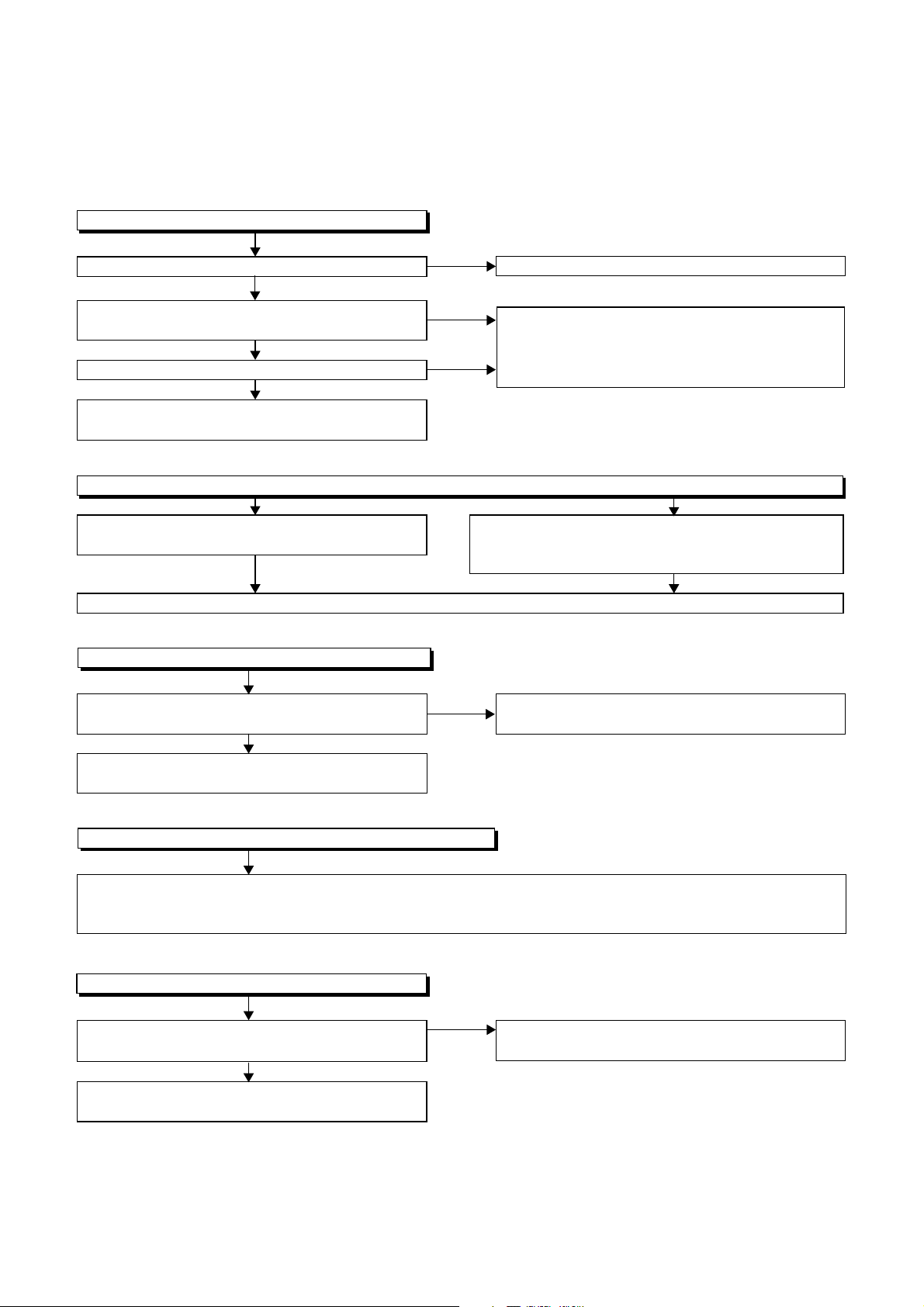
FLOW CHART NO.1
The power cannot be turned on.
TROUBLESHOOTING
Is the fuse normal?
Ye s
Is normal state restored when once unplugged
power cord is plugged again after several seconds.
Ye s
Is the AL+5V(1) line voltage normal?
Ye s
Check each rectifying circuit of secondary circuit
and service it if defective.
FLOW CHART NO.2
The fuse blows out.
Check the presence that the primary component
is leaking or shorted and service it if defective.
After servicing, replace the fuse.
FLOW CHART NO.3
When the output voltage fluctuates.
Does the secondary side photo coupler circuit
operate normally?
Ye s
Check the circuit and service it if defective.
(IC2101, D2111, D2112, D2113)
No
No
No
No
See FLOW CHART No.2 <The fuse blows out.>
Check for lead or short-circuiting of primary
circuit component and service it if defective.
(Q2101, Q2102, T2001, D2001, D2002, D2003,
D2004, R2101, R2102, R2103, R2104, R2105)
Check the presence that the rectifying diode or circuit
is shorted in each rectifying circuit of secondary side
and service it if defective.
Check the circuit and service it if defective.
(IC2101, IC2201, D2212, D2238, D2240)
FLOW CHART NO.4
When buzz sound can be heard in the vicinity of power circuit.
Check if there is short circuit on the rectifying diode and the circuit in each rectifying circuit of secondary side and
service it if defective. (D2201, D2202, D2203, D2204, D2205, D2206, D2207, D2208, D2209, D2231, D2232, D2233,
IC1025, IC1151, IC1152, Q1015, Q1154, Q1155, Q1156, Q1159, Q1160, Q1163, Q1508, Q1573, Q2203)
FLOW CHART NO.5
-FL is not outputted.
Is the supply voltage of -30V fed to the anode of
No
D2201?
Ye s
Check for load circuit short-circuiting or leak, and
service it if defective.
Check D2201 and their periphery, and service it if
defective.
1-10-1 E2J00TR
Page 23
FLOW CHART NO.6
AUDIO+10V is not outputted.
Is 12V voltage supplied to the collector of Q1160?
No
Is 12V voltage supplied to the collector of Q2203?
Ye s
Check Q2203, IC2204 and their periphery, and
service it if defective.
FLOW CHART NO.7
AL+9V is not outputted.
Is 12V voltage supplied to the collector of Q1156?
Ye s
Check Q1156, D1156 and their periphery, and
service it if defective.
FLOW CHART NO.8
P-ON+5V is not outputted.
(AUDIO+10V is outputted normally.)
Yes Check Q1160, D1162 and their periphery, and
service it if defective.
No
No
Check D2204, D2205, D2212, C2204 and their
periphery, and service it if defective.
Check D2204, D2205, D2212, C2204
TTand their periphery, and service it if defective.
Is 5V voltage supplied to the
Check Q1154 and their periphery, and service it if
defective.
FLOW CHART NO.9
EV+32V is not outputted.
Is the supply voltage 44V fed the cathode of D2202
Check D1701 and their periphery and service it
if defective.
FLOW CHART NO.10
AUDIO +5V is not outputted. (AUDIO+10V is outputted normally.)
Is 6V voltage supplied to the base of Q1163?
Replace Q1163.
collector
Ye s
Ye s
Ye s
of Q1154?
No
No
No
Check D2206, D2207, D2213, C2205, C2216
and their periphery, and service it if defective.
Check D2202, D2229, L2202 and their periphery,
and service it if defective.
Check D1163, C1168 and their periphery, and
service it if defective.
1-10-2 E2J00TR
Page 24
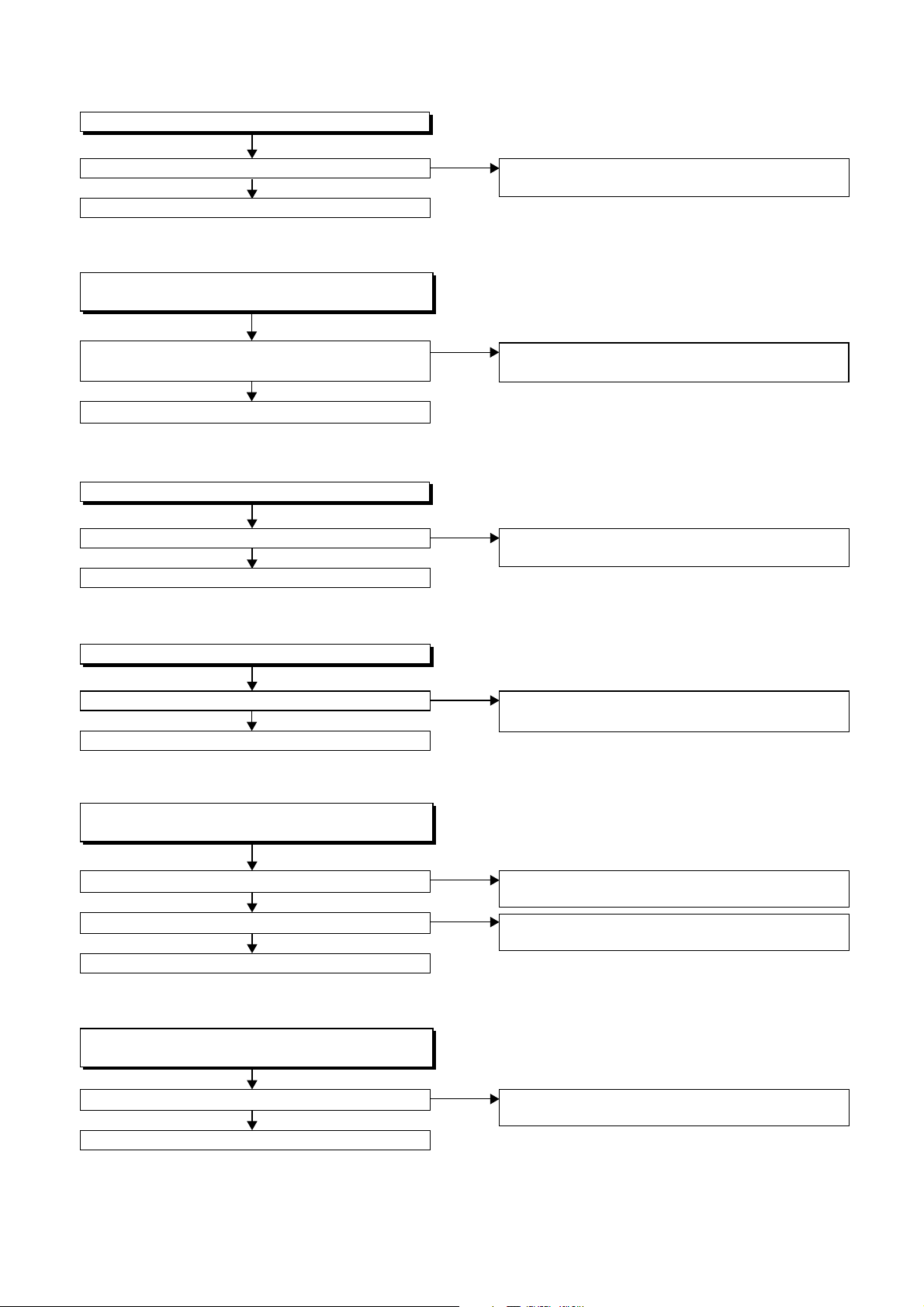
FLOW CHART NO.11
SYS+5V is not outputted.
Is 12V voltage supplied to Pin(3) of IC1025?
Ye s
Replace IC1025.
FLOW CHART NO.12
EV+3.3V is not outputted.
(SYS+5V is outputted normally.)
Is the voltage of approximately 4V supplied to
the base of Q1159?
Ye s
Replace Q1159.
FLOW CHART NO.13
P-ON+1.8V is not outputted.
Is 2.8V voltage supplied to Pin(1) of IC1151?
Ye s
Replace IC1151.
No
No
No
Check D2204, D2205, D2212, C2204
and their periphery, and service it if defective.
Check IC1153 and their periphery, and service it if
defective.
Check D2203, D2232, D2233, C2203, C2239
and their periphery, and service it if defective.
FLOW CHART NO.14
P-ON+3.3V is not outputted.
Is 5V voltage supplied to Pin(1) of IC1152?
Ye s
Replace IC1152.
FLOW CHART NO.15
TUNER+12V is not outputted.
(+32V is outputted normally.)
Is 14V voltage supplied to the collector of Q1573?
Ye s
Is 13V voltage supplied to the base of Q1573?
Ye s
Replace Q1573.
FLOW CHART NO.16
AL+5V(2) is not outputted.
(AL+9V is outputted normally.)
No
No
No
Check D1181, D1185, D2209, C2217
and their periphery, and service it if defective.
Check D2204, D2205, D2212, C2204
and their periphery, and service it if defective.
Check Q1571, Q1572 and their periphery,
and service it if defective.
Is 6V voltage supplied to the base of Q1508?
Ye s
Replace Q1508.
No
Check D1508, C1526
and their periphery, and service it if defective.
1-10-3 E2J00TR
Page 25
FLOW CHART NO.17
The key operation is not functioning.
Are the contact point and the installation state of
the key switches normal?
Ye s
Is the control voltage normally inputted into
Pin(1, 2) of IC009?
Ye s
Replace IC009 or DVD MECHANISM & DVD/HDD
MAIN CBA ASSEMBLY.
FLOW CHART NO.18
No operation is possible from the remote control unit. (
Is 5V voltage supplied to the Pin(3) terminal of
the RS1501 (remote control receiver)?
Ye s
Is the "L" pulse sent out from Pin(1) terminal of
the RS1501 (remote control receiver) when the
remote control unit is activated?
Ye s
Is the "L" pulse signal supplied to the Pin(27) of
IC009?
Ye s
Replace IC009 or DVD MECHANISM & DVD/HDD
MAIN CBA ASSEMBLY.
No
Re-install some key switches correctly or
replace some key switches.
No
Check the key switches and their periphery, and
service it if defective.
3.300
2.479
2.464
1.746
1.730
1.115
1.100
0.484
0.469
0.161
0.146
(V)
Operation is possible from the unit.)
No
No
Check AL+5V (1) line and service it if defective.
Replace the RS1501 (remote control receiver).
Or replace remote control unit.
No
Check the line between the RS1501 (remote
control receiver) and the Pin(27) of IC009, and
service it if defective.
KEYTerminal voltage of IC009-1,2 -1
IC009-1
REC DVD
PLAY
-----
POWER
KEY-2
IC009-2
----------
HDDSTOP
CH UP
CH
DOWN
OPEN
/CLOSE
FLOW CHART NO.19
The disc tray cannot be opened and closed. (It can be done using the remote control unit.)
Is the normal control voltage inputted to Pin(2) of
IC009?
Refer to "FLOW CHART NO.17" <The key
No
Replace the "OPEN/CLOSE" button (SW1643).
operation is not functioning.>
Ye s
Replace IC009 or DVD MECHANISM & DVD/HDD
MAIN CBA ASSEMBLY.
1-10-4 E2J00TR
Page 26

FLOW CHART NO.20
[No Disc] indicated.
Both functions of picture and sound do not operate normally.
Replace the DVD MECHANISM & DVD/HDD MAIN
CBA ASSEMBLY.
FLOW CHART NO.21
VIDEO E-E does not appear normally.
Are the video signals inputted to each pin of
IC005?
IC005 VIDEO-IN 1 (AV1)16PIN
IC005 VIDEO-IN (FRONT)14PIN
IC005 Y-IN 1 (FRONT)7PIN
IC005 C-IN 1 (FRONT)9PIN
IC005 VIDEO-IN 2 (AV2)12PIN
IC005 DTV-Y-IN100PIN
IC005 DTV-C-IN1PIN
IC005 TUNER-VIDEO
Are the video signals outputted to each pin of
IC005?
IC005 VIDEO-Y/CVBS-IN61PIN
IC005 VIDEO-C-IN59PIN
Are the video signals outputted to each pin of
CN1201?
CN1201 VIDEO-Y/CVBS-IN20PIN
CN1201 VIDEO-C-IN22PIN
Continued to A on the next page.
20PIN
Ye s
Ye s
Ye s
No
No
No
Check the line between video input terminal and
each pin of IC005.
IC
005
005
005
IC
IC
005
005
IC
005
IC
IC
005
IC
005
Is 5V voltage supplied to the Pin(27,29,47,63) of IC
Ye s
Replace IC005. Check AL+5V(2) line
Check the line between each pin of IC005 and
each pin of CN1201 and service it if defective.
IC
005
IC
005
→ JK120616PIN
→ JK120114PIN
→ JK12127PIN
→ JK12129PIN
→ JK120712PIN
→ CN1751100PIN
26PIN
→ CN17511PIN
28PIN
→ TU170120PIN
17PIN
and service it if defective.
→ CN120161PIN
→ CN1201 59PIN
VIDEO-IN 1 (AV1)
VIDEO-IN (FRONT)IC
Y-IN 1 (FRONT)
C-IN 1 (FRONT)
VIDEO-IN 2 (AV2)
DTV-Y
DTV-C
TUNER-VIDEO
No
20PIN
22PIN
VIDEO-Y/CVBS-IN
VIDEO-C-IN
005
?
1-10-5 E2J00TR
Page 27

A
Are the video signals outputted to each pin of
CN1201?
CN1201 VIDEO-Y(I/P)-OUT7PIN
CN1201 VIDEO-Y(I)-OUT1PIN
CN1201 VIDEO-Pr/Cr-OUT5PIN
CN1201 VIDEO-Pb/Cb-OUT3PIN
CN1201 VIDEO-C-OUT
Are the video signals shown above inputted into
each pin of IC005?
IC005 VIDEO-Y(I/P)-OUT51PIN
IC005 VIDEO-Y(I)-OUT55PIN
IC005 VIDEO-Pr/Cr-OUT52PIN
IC005 VIDEO-Pb/Cb-OUT53PIN
IC005 VIDEO-C-OUT57PIN
Are the video signals outputted to each pin of
IC005?
IC005 VIDEO-Y40PIN
IC005 VIDEO-Pr/Cr39PIN
IC005 VIDEO-Pb/Cb38PIN
IC005 VIDEO-OUT 1 (AV1)30PIN
IC005 VIDEO-OUT 2 (AV2)22PIN
9PIN
Ye s
Ye s
No
No
No
Replace the DVD MECHANISM & DVD/HDD MAIN
CBA ASSEMBLY.
Check the line between each pin of CN1201 and
each pin of IC005, and service it if defective.
CN1201 → IC
CN1201 → IC
CN1201 → IC
Is 5V voltage supplied to the Pin(27,29,47,63) of IC
Replace IC005. Check AL+5V(2) line
7PIN
1PIN 55PIN
5PIN
3PIN
→ IC
9PIN
Ye s
51PIN
005
005
005
52PIN
53PIN
005
005
57PINCN1201
and service it if defective.
VIDEO-Y(I/P)-OUT
VIDEO-Y(I)-OUTCN1201 → IC
VIDEO-Pr/Cr-OUT
VIDEO-Pb/Cb-OUT
VIDEO-C-OUT
005
?
No
Ye s
Are the video signals outputted to the specific
output terminal?
Are the Y, Pb/Cb, Pr/Cr signals outputted to the
COMPONENT OUT terminal (JK1205)?
Are the composite video signals outputted to
the VIDEO OUT (AV1) terminal (JK1206)?
Are the composite video signals outputted to
the VIDEO OUT (AV2) terminal (JK1207)?
No
No
No
Check the periphery of JK1205 from Pin (38,39,
40) of IC005 and service it if defective.
Check the periphery of JK1206 from Pin (30) of
IC005 and service it if defective.
Check the periphery of JK1207 from Pin (22) of
IC005 and service it if defective.
1-10-6 E2J00TR
Page 28

FLOW CHART NO.22
Picture does not appear normally.
Set the disc on the disc tray, and playback.
Are the video signals outputted to each pin of
CN1201?
CN1201 VIDEO-Y(I/P)-OUT7PIN
CN1201 VIDEO-Y(I)-OUT1PIN
CN1201 VIDEO-Pr/Cr-OUT5PIN
CN1201 VIDEO-Pb/Cb-OUT3PIN
CN1201 VIDEO-C-OUT
Are the video signals shown above inputted into
each pin of IC005?
IC005 VIDEO-Y(I/P)-OUT51PIN
IC005 VIDEO-Y(I)-OUT55PIN
IC005 VIDEO-Pr/Cr-OUT52PIN
IC005 VIDEO-Pb/Cb-OUT53PIN
IC005 VIDEO-C-OUT57PIN
Are the video signals outputted to each pin of
IC005?
IC005 VIDEO-Y40PIN
IC005 VIDEO-Pr/Cr39PIN
IC005 VIDEO-Pb/Cb38PIN
IC005 VIDEO-OUT 1 (AV1)30PIN
IC005 VIDEO-OUT 2 (AV2)22PIN
9PIN
Ye s
Ye s
No
No
No
Replace the DVD MECHANISM & DVD/HDD MAIN
CBA ASSEMBLY.
Check the line between each pin of CN1201 and
each pin of IC005, and service it if defective.
CN1201 → IC
CN1201 → IC
CN1201 → IC
Is 5V voltage supplied to the Pin(27,29,47,63) of IC
Replace IC005. Check AL+5V(2) line
7PIN
1PIN 55PIN
5PIN
3PIN
→ IC
9PIN
Ye s
51PIN
005
005
005
52PIN
53PIN
005
005
57PINCN1201
and service it if defective.
VIDEO-Y(I/P)-OUT
VIDEO-Y(I)-OUTCN1201 → IC
VIDEO-Pr/Cr-OUT
VIDEO-Pb/Cb-OUT
VIDEO-C-OUT
005
?
No
Ye s
Are the video signals outputted to the specific
output terminal?
Are the Y, Pb/Cb, Pr/Cr signals outputted to the
COMPONENT OUT terminal (JK1205)?
Are the composite video signals outputted to
the VIDEO OUT (AV1) terminal (JK1206)?
Are the composite video signals outputted to
the VIDEO OUT (AV2) terminal (JK1207)?
No
No
No
Check the periphery of JK1205 from Pin (38,39,
40) of IC005 and service it if defective.
Check the periphery of JK1206 from Pin (30) of
IC005 and service it if defective.
Check the periphery of JK1207 from Pin (22) of
IC005 and service it if defective.
1-10-7 E2J00TR
Page 29

FLOW CHART NO.23
Audio E-E does not appear normally.
Are the audio signals inputted to each pin of
IC005?
IC005 AUDIO-IN1 (AV1)93,94PIN
IC005 AUDIO-IN1 (FRONT)91,92PIN
IC005 AUDIO-IN2 (AV2)89,90PIN
IC005 DTV-AUDIO-IN81,82PIN
IC005 TUNER-AUDIO84,85PIN
No (Rear,
Front
or DTV
input)
No (Tuner)
Check the line between audio input terminal and
each pin of IC005, and service it if defective.
IC
005
005
005
005
91,92PIN
81,82PIN
IC
IC
IC
Is SIF signal inputted to Pin(2) of IC001?
Are the audio signal outputted
to Pin(30,31) of IC001?
Check the line between
Pin(30,31) of IC001 and
Pin(84,85) of IC005, and
service it if defective.
→
JK120693,94PIN
→
JK1202,
JK1203
→
JK120789,90PIN
→
CN1751
29,30PIN
Ye s
Ye s
AUDIO-IN1 (AV1)
AUDIO-IN1 (FRONT)
AUDIO-IN2 (AV2)
DTV-AUDIO-IN
No
Replace TU1701.
No
Replace IC001.
Ye s
Are the audio signals outputted to Pin(79,80) of
IC005?
Ye s
Are the audio signals outputted to Pin(1,7) of
IC1203?
Ye s
Continued to B on the next page.
No
No
Is 5V voltage supplied to Pin(63) of IC005?
Is 9V voltage supplied to Pin(75) of IC005?
Ye s N o
Replace IC005.
Replace IC1203.
Check the AL+5V(2) , AL+9V
line and service it if defective.
1-10-8 E2J00TR
Page 30

B
Are the analog audio signals outputted to each pin
of CN1201?
CN1201 17PIN AUDIO (L)-OUT
CN1201 15PIN AUDIO (R)-OUT
Ye s
Are the analog audio signals inputted to each pin
of IC1202?
IC1202 6PIN AUDIO (L)-OUT
IC1202 2PIN AUDIO (R)-OUT
Ye s
Is the signal at Pin(18) of CN1201 "H"?
Ye s
Is the signal at Pin(37) of IC009 "H"?
Ye s
Are the analog audio signals outputted to each pin
of IC1202?
IC1202 7PIN AUDIO (L)-OUT
IC1202 1PIN AUDIO (R)-OUT
Ye s
Are the analog audio signals inputted to each pin
of IC005?
IC005 77PIN AUDIO (L)-OUT
IC005 76PIN AUDIO (R)-OUT
Ye s
Are the analog audio signals outputted to each pin
of IC005?
IC005 73,74PIN AUDIO-OUT 1 (AV1)
IC005 71,72PIN AUDIO-OUT 2 (AV2)
IC005 67,68PIN AUDIO-OUT 2 (REAR)
Ye s
Are the audio signals outputted to the specific
output terminal?
Are the audio signals outputted to the audio
terminal (JK1206)?
Are the audio signals outputted to the audio
terminal (JK1207)?
Are the audio signals outputted to the audio
terminal (JK1204)?
No
No
No
No
No
No
No
No
No
No
Replace the DVD MECHANISM & DVD/HDD MAIN
CBA ASSEMBLY.
Check each line between each pin of CN1201
and each pin of IC1202, and service it if defective.
CN1201 17PIN → IC1202 6PIN AUDIO(L)-OUT
CN1201 15PIN → IC1202 2PIN AUDIO(R)-OUT
Replace the DVD MECHANISM & DVD/HDD MAIN
CBA ASSEMBLY.
Check the line between pin(18) of CN1201
and pin(37) of IC009, and service it if defective.
Replace IC1202.
Check each line between each pin of IC1202
and each pin of IC005, and service it if defective.
IC1202 7PIN → IC005 77PIN AUDIO(L)-OUT
IC1202 1PIN → IC005 76PIN AUDIO(R)-OUT
Is 5V voltage supplied to Pin(63) of IC005?
Is 9V voltage supplied to Pin(75) of IC005?
Ye s N o
Replace IC005.
Check the periphery between Pin(73,74) of IC005
and the audio terminal (JK1206), and service it if
defective.
Check the periphery between Pin(71,72) of IC005
and the audio terminal (JK1207), and service it if
defective.
Check the periphery between Pin(67,68) of IC005
and the audio terminal (JK1204), and service it if
defective.
Check the AL+5V(2) , AL+9V
line and service it if defective.
1-10-9 E2J00TR
Page 31

FLOW CHART NO.24
Audio is not outputted during playback.
Set the disc on the disc tray, and playback.
Are the analog audio signals outputted to each pin
of CN1201?
CN1201 17PIN AUDIO (L)-OUT
CN1201 15PIN AUDIO (R)-OUT
Ye s
Are the analog audio signals inputted to each pin
of IC1202?
IC1202 6PIN AUDIO (L)-OUT
IC1202 2PIN AUDIO (R)-OUT
Ye s
Is the signal at Pin(18) of CN1201 "H"?
Ye s
Is the signal at Pin(37) of IC009 "H"?
Ye s
Are the analog audio signals outputted to each pin
of IC1202?
IC1202 7PIN AUDIO (L)-OUT
IC1202 1PIN AUDIO (R)-OUT
Ye s
Are the analog audio signals inputted to each pin
of IC005?
IC005 77PIN AUDIO (L)-OUT
IC005 76PIN AUDIO (R)-OUT
Ye s
Are the analog audio signals outputted to each pin
of IC005?
IC005 73,74PIN AUDIO-OUT 1 (AV1)
IC005 71,72PIN AUDIO-OUT 2 (AV2)
IC005 67,68PIN AUDIO-OUT 2 (REAR)
Ye s
Are the audio signals outputted to the specific
output terminal?
Are the audio signals outputted to the audio
terminal (JK1206)?
Are the audio signals outputted to the audio
terminal (JK1207)?
Are the audio signals outputted to the audio
terminal (JK1204)?
No
No
No
No
No
No
No
No
No
No
Replace the DVD MECHANISM & DVD/HDD MAIN
CBA ASSEMBLY.
Check each line between each pin of CN1201
and each pin of IC1202, and service it if defective.
CN1201 17PIN → IC1202 6PIN AUDIO(L)-OUT
CN1201 15PIN → IC1202 2PIN AUDIO(R)-OUT
Replace the DVD MECHANISM & DVD/HDD MAIN
CBA ASSEMBLY.
Check the line between pin(18) of CN1201
and pin(37) of IC009, and service it if defective.
Replace IC1202.
Check each line between each pin of IC1202
and each pin of IC005, and service it if defective.
IC1202 7PIN → IC005 77PIN AUDIO(L)-OUT
IC1202 1PIN → IC005 76PIN AUDIO(R)-OUT
Is 5V voltage supplied to Pin(63) of IC005?
Is 9V voltage supplied to Pin(75) of IC005?
Ye s N o
Replace IC005.
Check the periphery between Pin(73,74) of IC005
and the audio terminal (JK1206), and service it if
defective.
Check the periphery between Pin(71,72) of IC005
and the audio terminal (JK1207), and service it if
defective.
Check the periphery between Pin(67,68) of IC005
and the audio terminal (JK1204), and service it if
defective.
Check the AL+5V(2) , AL+9V
line and service it if defective.
1-10-10 E2J00TR
Page 32

BLOCK DIAGRAMS
System Control Block Diagram
FAN
TO DTV MODULE
1 FAN-VCC
CN1601
Q1601
2 GND
Q1603
3 IF-AGC
CN1751
ASSEMBLY
4 TU-SDA
5 TU-SCL
Q1602
Q1604
SCL
TU1751 (TUNER UNIT)
14
TO VIDEO
BLOCK DIAGRAM
TO AUDIO
BLOCK DIAGRAM
SCL
SDA
DAVN-L
IF AGC
SDA
18
15
DVD/HDD-AUDIO-MUTE
SDA
AUDIO-MUTE
SC-AUDIO-MUTE
Q1506
SCL
Q1507
FL1501
SCL
SDA
TU1701(TUNER UNIT)
9
10
IC1503 (VFD DRIVER)
23
1G
DIN
28
GRID VFD
~
~
CLK
1
POWER
SW3010
CN1064
POW-SW 1
SEGMENT
~
7
16
a
14
~
h
REMOTE
RS1501
i
SENSOR
17
7G
STB
2
1
CN1063
KEY SWITCH
CN1062
KEY-1 2
2
CN1651
KEY SWITCH
KEY-2 4
4
SW CBA POWER SW CBA
EV+12V
IC009
(SUB MICRO CONTROLLER)
1V2CONT
REG-CONT
PWR-SW
DTV1.05-CONT
525346
LOW-POW
REG-CONT
PWR-SW
DTV1.05-CONT
16
15
FAN-CONT2
FAN-CONT1
LOW-POWER
RESET
17
14
12
RESET
IC1502
Q1504
RESET
SW1501
P-DOWN
30
BUP+3.3V
7
C1509
(BACKUP CAPACITOR)
Q1505
XOUT
8
X1502
8MHz
XIN
9
RESONATOR
24
DAVN-L
XCOUT
12
32.768KHz
X1501
38
37
AUDIO-MUTE
DVD/HDD-AUDIO-MUTE
XCIN
11
X'TAL
EV+2.8VP-ON+1.2V
393334
SCL
SDA
SC-AUDIO-MUTE
1V2CONT
26
111V2CONT
CN101 CN1151
IC107
RESET
2 1
48
50
FL-DIN
FL-CLK
SUB-RXD
SYS-RESET
2219182029
CN1201
27 27SYS-RESET
30 30SUB-RXD
CN701
R2
V25
R25
49
27
FL-STB
REMOTE
SUB-TXD
SUB-SCLK
RDY
28 28SUB-TXD
26 26SUB-SCLK
29 29RDY
B4
P22
W26
X501
IC501
27MHz
X'TAL
4 2
L1
STANDBY
UARTI-RXD
UARTI-TXD
SYS-RESET
55
44
33
22
CN503 CN1753
A4
R23
R22
W25
1
KEY-1
2
KEY-2
CN1751
121514
SYS-RESET
13
STANDBY
UARTI-RXD
UARTI-TXD
TO DTV MODULE
ASSEMBLY
AV CBA
TO POWER SUPPLY
BLOCK DIAGRAM
EV+3.3V
SYS+5V
IC106
+1.2V
REGULATOR
P-ON+1.8V
1-11-1
IC101
(MAIN MICRO CONTROLLER)
SUB-TXD
SUB-RXD
SYS-RESET
SYS-RESET
RDY
SUB-SCLK
CLK 27 IN
UARTI-TXD
UARTI-RXD
SYS-RESET
DVD/HDD MAIN CBA UNIT
SYS-RESET
E2J00BLS
Page 33

Digital Signal Process Block Diagram
TO VIDEO
BLOCK
DIAGRAM
(CN1201)
7
1
3
5
20
TO AUDIO
BLOCK
DIAGRAM
(CN1151)
TO AUDIO
BLOCK
DIAGRAM
(CN1201)
17
15
18
13
TO HDMI
HDMI-SDA
YC(0-7)
D6,D7
C6,C7,
A5,B5-B7,
REC VIDEO SIGNAL PB VIDEO SIGNAL REC AUDIO SIGNAL PB AUDIO SIGNAL
BLOCK
DIAGRAM
HDMI-SCL
CLOCK-PULSE
C5
N23
U25
HDMI-SCL
HDMI-SDA
CLOCK-PULSE
VIDEO
I/F
F2
D/A
CN701
J3
K5
D/A
D/A
VIDEO
ENCODER
VIDEO-Y(I/P)-OUT
VIDEO-Y(I)-OUT
VIDEO-C-OUT9VIDEO-C-IN 22
VIDEO-Pb/Cb-OUT
VIDEO-Pr/Cr-OUT
F1
D/A
IC701 (VIDEO DECODER)
U4,W1,W3,
VIDEO-Y/CVBS-IN
10813
A/D
DECODER A/D
DECODER
45-50
39-44
U2,U3,V1
P3,T3,T5,
Y2,AA1,AA2
TO HDMI
BLOCK
SPDIF
PCM-BCK
PCM-DATA0
P1
N2
M1N3M2
CN101
DIAGRAM
PCM-SCLK
PCM-LRCK
SPDIF 3
CN701
AUDIO(L)-OUT
AUDIO(R)-OUT
D1
D3
AUDIO D/A
CONVERTER
AUDIO
I/F
DVD/HDD-AUDIO-MUTE
AUDIO(L)-IN11AUDIO(R)-IN
13
14
R-CH
L-CH
IC802
(AUDIO A/D CONVERTER)
101112
T23
DVD-AUDIO-MUTE
E12
AIMS
MD
Y26
U24
MC
AUDIO A/D
CONVERTER
7
6
K2
M3
LRCK
SYSCLK
BCK
8
K1
9
N4
DATA
TO 1394
CABLE
(W1)
1 TPA1P
CN901
IC901 (IEEE1394 I/F)
430567
Y5
AA3
AC2
2 TPA1N
4 TPB1P
292827
RECEIVE
DATA
DECODER
LINK
8
9
AB3
AA4
AC3
LINK
5 TPB1N
I/F
10
AE1
I/F
TRANSMIT
DATA
1482
11
AA5
AD1
ENCODER
3
Y4
W5
AC1
(MAIN MICRO CONTROLLER)
IC101
CN3001 CN3002 CN651
IC201
ATA CBA
RF/
ERROR
AMP
CN201
LPC
TILT
PICK
IC301
TRACKING
-UP
BACK-END
DIGITAL
FOCUS
SIGNAL
PROCESS
FRONT-END
DIGITAL
SIGNAL
MOTOR
DRIVER
PROCESS
TRAY OPEN
CN301
CN1001
IC202
+3.3V
OP AMP
IC302
MOTOR
DRIVER
IC104, IC105
(FLASH MEMORY)
CN1002
FLASH MEMORY
DDR SDRAM
IC102 (DDR SDRAM)
DVD/HDD MAIN CBA UNIT
RELAY CBA
HARD
DISK
DRIVE
DVD MECHANISM
1-11-2
SLED
MOTOR
M
SPINDLE
MOTOR
M
E2J00BLD
Page 34

Video Block Diagram
VIDEO
IN2
JK1206
20
JK1201
(FRONT)
IN1
VIDEO-IN
VIDEO
JK1207
20
AV CBA
VIDEO OUT
TU1701
(TUNER UNIT)
17
DIF-OUT2
TU1751
(TUNER UNIT)
20
DIF-OUT1
21
DTV SIGNAL
ASSEMBLY
DIF-OUT12DIF-OUT2
1
CN1751
PROCESS
DTV-Y28DTV-C
26
DTV MODULE
JK1212
(FRONT)
YC
S-VIDEO
IN
G G
IC1641 (VPS)
VPS-V
SDA
642
16
SCL
7
DAVN-L
14
DAVN-L
TO SYSTEM CONTROL
SCL
BLOCK DIAGRAM
SDA
REC VIDEO SIGNAL PB VIDEO SIGNAL
SW
1262161420
SW
64
GCL
LPF
SW
7
100
SW
SW
65
SW
AGC
SW
1
9
+
SW
AGC
SW
LPF
SW
43
I/F
IIC
(VIDEO SIGNAL PROCESS)IC005
DRIVER FBC
224850
BUFFER
Q1853
JK1207
19
VIDEO OUT2
7
11
VIDEO-B
VIDEO-G
49
15
VIDEO-R
MUTE
61
BUFFER
Q1202
MUTE
59
BUFFER
Q1201
SW
5152535557
WF1
WF5
CN1201
VIDEO-Y/CVBS-IN
VIDEO-Y(I/P)-OUT
7
20
22 VIDEO-C-IN
TO DIGITAL
SIGNAL
VIDEO-Pr/Cr-OUT
VIDEO-Pb/Cb-OUT
VIDEO-Y(I)-OUT
VIDEO-C-OUT
5
3
1
9
PROCESS
BLOCK
DIAGRAM
(CN701)
+
WF4WF2
MUTE FBC
DRIVER
30
WF3
BUFFER
Q1204
JK1206
19
VIDEO OUT1
1-11-3
DRIVER
46
11715
VIDEO-B
VIDEO-G
DRIVER
44
VIDEO-R
DRIVER
45
JK1205
(REAR)
SW
DRIVER
40
VIDEO-Y
-OUT
DRIVER
38
VIDEO-Pb/Cb
-OUT
DRIVER
39
VIDEO-Pr/Cr
-OUT
E2J00BLV
Page 35

Audio Block Diagram
AUDIO(R)-IN2
AUDIO(L)-OUT2
AUDIO(R)-OUT2
AUDIO(L)-IN2
613
JK1207
2
MUTE-ON
MUTE-ON
JK1206
Q1852
Q1851
AUDIO(R)-IN1
AUDIO(L)-OUT1
AUDIO(L)-IN1
2
613
AUDIO(R)-OUT1
MUTE-ON
Q1805
DTV MODULE
DIF-OUT2
TU1751
(TUNER UNIT)
20
ASSEMBLY
DIF-OUT12DIF-OUT2
1
CN1751
DIF-OUT1
21
DTV SIGNAL
PROCESS
DTV-AUDIO(L)30DTV-AUDIO(R)
29
(REAR)
JK1204
AUDIO OUT
SIF OUT
TU1701
(TUNER UNIT)
6
7
2
43
IF SIGNAL
PROCESS
IC001
(IF SIGNAL PROCESS)
30
31
AUDIO(L)
-OUT
MUTE-ON
Q1806
AUDIO(R)
-OUT
MUTE-ON
Q1803
Q1807
DIGITAL
AUDIO OUT
BUFFER
(COAXIAL)
Q1802
DRIVE
(FRONT)
JK1202
AUDIO(L)
-IN
AUDIO(R)
(FRONT)
JK1203
-IN
TO SYSTEM CONTROL
BLOCK DIAGRAM
REC AUDIO SIGNAL PB AUDIO SIGNAL
72
SW
Q1801
DRIVE
MUTE-ON
Q1804
AUDIO-MUTE
SC-AUDIO-MUTE
DVD/HDD-AUDIO-MUTE
67
71
SW
74
SW
73
SW
68
SW
SW
90
948592
82
8993849181
IC005 (AUDIO SIGNAL PROCESS)
SDA
AV CBA
IIC
42
TO SYSTEM CONTROL
SCL
BLOCK DIAGRAM
)
OP AMP
(
IC1203
OP
SW
80
6
AMP
7
SW
I/F
(OP AMP)
IC1202
OP
77
7
AMP
6
43
OP
76
1
AMP
2
WF6
CN1201
AUDIO(L)-OUT
AUDIO(R)-OUT
DVD/HDD-AUDIO-MUTE
AUDIO(L)-IN13AUDIO(R)-IN
17
15
18
11
TO DIGITAL
SIGNAL
PROCESS
BLOCK
DIAGRAM
(CN701)
SW
1-11-4
OP
79
2
1
SW
AMP
CN1151
SPDIF
3
TO DIGITAL
SIGNAL
PROCESS
BLOCK
E2J00BLA
DIAGRAM
(CN101)
WF7
Page 36

HDMI Block Diagram
CNA01
+3.3V
HOT PLUG DETECT
DDC DATA
DDC CLOCK
HDMI-CONNECTOR
151916
6
5
T.M.D.S DATA2-
T.M.D.S DATA2+
T.M.D.S DATA1-
T.M.D.S DATA1+
T.M.D.S DATA0-
T.M.D.S DATA0+
T.M.D.S CLOCK+
649
3
1
7
T.M.D.S CLOCK-
10
12
REC AUDIO SIGNAL PB AUDIO SIGNAL
REC VIDEO SIGNAL PB VIDEO SIGNAL
QA01
ICA02
3.3V<-->5V
CONVERTER
119
AUTHENT
3
2
120
121
DDC
I/F
/CATION
KEY
EXCHANGE
22
24
1820141612
TMDS
SERIALIZER
TMDS
ENCODER
HDCP
CIPHER/
ENCRYPTOR
10
DVD/HDD MAIN CBA UNIT
ICA01 (HDMI INTERFACE)
HDMI-SCL
REGISTER
IIC
I/F
113
114
HDMI-SDA
AUDIO
I/F
433341
38
PCM-DATA0
SPDIF
PCM-SCLK
PCM-LRCK
TO DIGITAL SIGNAL
AV
CONTROLLER
45
81
83~86
PCM-BCK
PROCESS BLOCK
DIAGRAM
VIDEO
I/F
YC(0-7)
~
90
PCLK
117
111
CLOCK-PULSE
1-11-5
E2J00BLHD
Page 37

Power Supply Block Diagram
TO HARD
DISK DRIVE
1 HDD+5V
CN1015
4 HDD+12V
TO DVD/HDD
MAIN CBA UNIT
(CN101)
10-12 AL+2.8V
CN1151
15-17 P-ON+3.3V
20-22 P-ON+5V
25-27 EV+10.5V
TO DTV
MODULE
P-ON+1.8V
6,7
ASSEMBLY
TUNER+12V
20
CN1751
P-ON+1.8V
P-ON+3.3V
8
10
-FL
EV+32V
SYS+5V
EV+3.3V
+3.3V REG.
Q1159
+5V REG.
IC1025
CAUTION !
Fixed voltage (or Auto voltage selectable) power supply circuit is used in this unit.
If Main Fuse (F2001) is blown , check to see that all components in the power supply
circuit are not defective before you connect the AC plug to the AC power supply.
Otherwise it may cause some components in the power supply circuit to fail.
Q1025
REG
IC1153
SHUNT
REGULATOR
EV+12V
AL+9V
+9V REG.
Q1156
AL+5V(2)
Q1508
+5V REG.
SW+12V
Q1573
23-28
29-32
AL+5V(1)
Q1572
Q1571
19-22
Q1015
Q2203
AUDIO+5V
+5V REG.
Q1163
+10V REG.
Q1160
Q2221
REG
PWR-SW
1V2CONT
Q1016
IC2204
SHUNT
TO SYSTEM
CONTROL
BLOCK
DIAGRAM
LOW-POW
REG-CONT
DTV1.05-CONT
Q1154
REGULATOR
P-ON+3.3V
SW+5V
Q1155
P-ON+10V
P-ON+5V
F1
F2
Q1753
+1.8V REG.
IC1751
AV CBAPOWER SUPPLY CBA
Q1164
+3.3V REG.
IC1152
Q1165
+1.8V REG.
IC1151
16
15
NOTE:
The voltage for parts in hot circuit is measured using
hot GND as a common terminal.
T2001
3
BRIDGE
RECTIFIER
D2001-D2004
LINE
L2001
FILTER
F2001
CAUTION !
HOT CIRCUIT. BE CAREFUL.
For continued protection against fire hazard,
replace only with the same type fuse.
T2.0A L 250V
2 -FL 2
CN2001 CN1152
14
5
33 EV+33V 33
EV+12V
AL+2.8V
23-28
29-32
13
5,6 REG-VCC 5,6
Q2101
AL+5V(1)
4F1 4
3F2 3
19-22
12
1 LOW-POW 1
Q2209
COLD
9
IC2101
8
ERROR
VOLTAGE DET
1
4
23
REG
IC2201
SHUNT
REGULATOR
HOT
Q2102
11
10
7
AC2001
1-11-6
E2J00BLP
Page 38

SCHEMATIC DIAGRAMS / CBA’S AND TEST POINTS
Standard Notes
WARNING
Many electrical and mechanical parts in this chassis
have special characteristics. These characteristics
often pass unnoticed and the protection afforded by
them cannot necessarily be obtained by using
replacement components rated for higher voltage,
wattage, etc. Replacement parts that have these
special safety characteristics are identified in this
manual and its supplements; electrical components
having such features are identified by the mark " ! "
in the schematic diagram and the parts list. Before
replacing any of these components, read the parts list
in this manual carefully. The use of substitute
replacement parts that do not have the same safety
characteristics as specified in the parts list may create
shock, fire, or other hazards.
Notes:
1. Do not use the part number shown on these
drawings for ordering. The correct part number is
shown in the parts list, and may be slightly different
or amended since these drawings were prepared.
2. All resistance values are indicated in ohms
3
(K=10
3. Resistor wattages are 1/4W or 1/6W unless
otherwise specified.
4. All capacitance values are indicated in µF
(P=10
5. All voltages are DC voltages unless otherwise
specified.
6. Electrical parts such as capacitors, connectors,
diodes, IC’s, transistors, resistors, switches, and
fuses are identified by four digits. The first two
digits are not shown for each component. In each
block of the diagram, there is a note such as shown
below to indicate these abbreviated two digits.
, M=106).
-6
µF).
1-12-1 H4P_SC
Page 39

LIST OF CAUTION, NOTES, AND SYMBOLS USED IN THE SCHEMATIC DIAGRAMS ON
THE FOLLOWING PAGES:
1. CAUTION:
FOR CONTINUED PROTECTION AGAINST FIRE HAZARD, REPLACE ONLY WITH THE SAME TYPE FUSE.
2. CAUTION:
Fixed Voltage (or Auto voltage selectable) power supply circuit is used in this unit.
If Main Fuse (F2001) is blown, first check to see that all components in the power supply circuit are not
defective before you connect the AC plug to the AC power supply. Otherwise it may cause some components
in the power supply circuit to fail.
3. Note:
1. Do not use the part number shown on the drawings for ordering. The correct part number is shown in the
parts list, and may be slightly different or amended since the drawings were prepared.
2. To maintain original function and reliability of repaired units, use only original replacement parts which are
listed with their part numbers in the parts list section of the service manual.
4. Voltage indications for PLAY and REC modes on the schematics are as shown below:
The same voltage for
both PLAY & REC modes
5. How to read converged lines
1-D3
Distinction Area
Line Number
(1 to 3 digits)
Examples:
1. "1-D3" means that line number "1" goes to the line number
"1" of the area "D3".
2. "1-B1" means that line number "1" goes to the line number
"1" of the area "B1".
6. Test Point Information
: Indicates a test point with a jumper wire across a hole in the PCB.
: Used to indicate a test point with a component lead on foil side.
: Used to indicate a test point with no test pin.
231
5.0
5.0
(2.5)
Indicates that the voltage
is not consistent here.
PLAY mode
REC mode
Unit: Volts
3
AREA D3
2
1
AREA B1
1-D3
ABCD
1-B1
: Used to indicate a test point with a test pin.
1-12-2 H4P_SC
Page 40

AV 1/5 Schematic Diagram
* NOTE
IC1502
BU4219G-TR
/R3112N191A-TR-FA
/R3112N191A-TR-FB
PST3619NR
Group A Group B
C1507 0.015 0.1
These components (IC1502, C1507)
can be used in any models.
However, you cannot mix components under
Group A with the ones under Group B.
You can choose either Group. The difference
between Group A and Group B is shown below.
1-12-3
E2J00SCAV1
Page 41

AV 2/5 Schematic Diagram
7G 6G 5G 4G 3G 2G 1G
a
b
c
d
e
f
g
c
d
e
f
gg
c
d
e
f
g
c
d
e
f
g
c
d
e
f
g
c
d
e
f
g
hh
i
ababababa
b
FL1501 MATRIX CHART
REPEAT
PM
REC
VCD VCR DVD
R
XP
SP
LP
EP
SLP
P.SCAN
SEP
W
CD
T
C
7G
h
REC
g
PM
h
REPEAT
6G
5G 4G 3G 2G 1G
VCD VCR
CD
T C
c
DVD
a
d
g
R
XP SP
b
LP EP
SLP
ef
P.SCAN
W
SEP
1-12-4
E2J00SCAV2
Page 42

AV 3/5 Schematic Diagram
1-12-5
E2J00SCAV3
Page 43

AV 4/5 Schematic Diagram
1-12-6
E2J00SCAV4
Page 44

AV 5/5 Schematic Diagram
1-12-7
E2J00SCAV5
Page 45

Power Supply Schematic Diagram
NOTE:
The voltage for parts in hot circuit is measured using
hot GND as a common terminal.
CAUTION !
Fixed voltage (or Auto voltage selectable) power supply circuit is used in this unit.
If Main Fuse (F2001) is blown , check to see that all components in the power supply
circuit are not defective before you connect the AC plug to the AC power supply.
Otherwise it may cause some components in the power supply circuit to fail.
CAUTION !
For continued protection against fire hazard,
replace only with the same type fuse.
1-12-8
E2J00SCP
Page 46

SW & Power SW Schematic Diagram
ATA Schematic Diagram
1-12-9
E2J00SCSW
E2J00SCATA
Page 47

DVD/HDD MAIN 1/7 Schematic Diagram
1 NOTE:
The order of pins shown in this diagram is different from that of actual IC101.
IC101 is divided into six and shown as IC101 (1/6) ~ IC101 (6/6) in this DVD/HDD Main Schematic Diagram Section.
1-12-10
E2J00SCD1
Page 48

DVD/HDD MAIN 2/7 Schematic Diagram
1 NOTE:
The order of pins shown in this diagram is different from that of actual IC101.
IC101 is divided into six and shown as IC101 (1/6) ~ IC101 (6/6) in this DVD/HDD Main Schematic Diagram Section.
1-12-11
E2J00SCD2
Page 49

DVD/HDD MAIN 3/7 Schematic Diagram
1 NOTE:
The order of pins shown in this diagram is different from that of actual IC101.
IC101 is divided into six and shown as IC101 (1/6) ~ IC101 (6/6) in this DVD/HDD Main Schematic Diagram Section.
1-12-12
E2J00SCD3
Page 50

DVD/HDD MAIN 4/7 Schematic Diagram
1 NOTE:
The order of pins shown in this diagram is different from that of actual IC101.
IC101 is divided into six and shown as IC101 (1/6) ~ IC101 (6/6) in this DVD/HDD Main Schematic Diagram Section.
1-12-13
E2J00SCD4
Page 51

DVD/HDD MAIN 5/7 Schematic Diagram
1 NOTE:
The order of pins shown in this diagram is different from that of actual IC101.
IC101 is divided into six and shown as IC101 (1/6) ~ IC101 (6/6) in this DVD/HDD Main Schematic Diagram Section.
1-12-14
E2J00SCD5
Page 52

DVD/HDD MAIN 6/7 Schematic Diagram
1-12-15
E2J00SCD6
Page 53

DVD/HDD MAIN 7/7 Schematic Diagram
1 NOTE:
The order of pins shown in this diagram is different from that of actual IC101.
IC101 is divided into six and shown as IC101 (1/6) ~ IC101 (6/6) in this DVD/HDD Main Schematic Diagram Section.
1-12-16
E2J00SCD7
Page 54

AV CBA Top View
1-12-17
BE2J70F01013A
Page 55

AV CBA Bottom View
PIN 17 OF
CN1201
WF2
PIN 9 OF
CN1201
WF1
PIN 7 OF
CN1201
WF5WF6
PIN 5 OF
CN1201
WF4
PIN 3 OF
CN1201
WF7
PIN 3 OF
CN1151
WF3
PIN 30 OF
IC005
1-12-18
BE2J70F01013A
Page 56

Power Supply CBA Top View
Because a hot chassis ground is present in the power
supply circut, an isolation transformer must be used.
Also, in order to have the ability to increase the input
slowly, when troubleshooting this type power supply
circuit, a variable isolation transformer is required.
CAUTION !
For continued protection against fire hazard,
replace only with the same type fuse.
NOTE:
The voltage for parts in hot circuit is measured using
hot GND as a common terminal.
CAUTION !
Fixed voltage (or Auto voltage selectable) power supply circuit is used in this unit.
If Main Fuse (F2001) is blown , check to see that all components in the power supply
circuit are not defective before you connect the AC plug to the AC power supply.
Otherwise it may cause some components in the power supply circuit to fail.
1-12-19
BE2J70F01021
Page 57

Power Supply CBA Bottom View
CAUTION !
For continued protection against fire hazard,
replace only with the same type fuse.
NOTE:
The voltage for parts in hot circuit is measured using
hot GND as a common terminal.
CAUTION !
Fixed voltage (or Auto voltage selectable) power supply circuit is used in this unit.
If Main Fuse (F2001) is blown , check to see that all components in the power supply
circuit are not defective before you connect the AC plug to the AC power supply.
Otherwise it may cause some components in the power supply circuit to fail.
Because a hot chassis ground is present in the power
supply circut, an isolation transformer must be used.
Also, in order to have the ability to increase the input
slowly, when troubleshooting this type power supply
circuit, a variable isolation transformer is required.
1-12-20
BE2J70F01021
Page 58

SW CBA Top View
Power SW CBA
Top View
Power SW CBA
Bottom View
BE2J70F01013C
SW CBA Bottom View
ATA CBA Top View
ATA CBA Bottom View
1-12-21
BE2J70F01013B
BE4340F01032
Page 59

WF1
Pin 7 of CN1201
WAVEFORMS
WF5
Pin 5 of CN1201
VIDEO-Y 0.2V 20µsec
WF2
Pin 9 of CN1201
VIDEO-C 0.2V 20
Pin 30 of IC005
WF3
VIDEO-Cr
WF6
Pin 17 of CN1201
µ
sec
AUDIO(L)-OUT
WF7
Pin 3 of CN1151
0.2V 20µsec
1V 0.5ms
VIDEO-CVBS 0.5V 20
WF4
Pin 3 of CN1201
VIDEO-Cb
0.2V 20µsec
µ
µ
sec
SPDIF 1V 0.1
sec
NOTE:
Input: COLOR BAR SIGNAL
(WITH 1KHz AUDIO SIGNAL)
1-13-1
HD4PWF
Page 60

Wiring 1/2 Diagram
WIRING DIAGRAM
CN101
GND 30
GND 29
GND 28
1
CN701
VIDEO-Y(I)-OUT
GND 2
VIDEO-Pb/Cb-OUT3GND 10
EV+10.5V 27
EV+10.5V 26
EV+10.5V 25
GND 24
5
7
GND 4
VIDEO-Pr/Cr-OUT
GND 6
VIDEO-Y(I/P)-OUT
W2
CONTINUE
WIRING
DIAGRAM 2/2
(CN1151)
CN503
GND 23
P-ON+5V 22
P-ON+5V 21
P-ON+5V 20
GND 19
GND 18
P-ON+3.3V 17
P-ON+3.3V 16
P-ON+3.3V 15
GND 14
GND 13
AL+2.8V 12
AL+2.8V 11
AL+2.8V 10
GND 9
GND 8
P-ON+1.8V 7
P-ON+1.8V 6
GND 5
GND 4
SPDIF 3
GND 2
1V2CONT 1
CONTINUE
WIRING
DIAGRAM 2/2
(CN1201)
15
17
18
19
21
23
GND 12
AUDIO(R)-IN 13
GND 14
GND 16
AUDIO(R)-OUT
AUDIO(L)-OUT
DVD/HDD-AUDIO-MUTE
AUDIO+5V20VIDEO-Y/CVBS-IN
GND22VIDEO-C-IN
GND24GND
GND25SUB-SCLK 26
AUDIO(L)-IN 11
VIDEO-C-OUT 9
GND 8
30
CNA01
SYS-RESET 27
SUB-TXD28RDY 29
SUB-RXD
REAR
HDMI
CONNECTOR
CN901
GND 1
CONTINUE
WIRING
UARTI-TXD 3
SYS-RESET 2
W1
TPA1P 1
TPA1N 2
W4
DIAGRAM 2/2
(CN1753)
NU 6
STANDBY 5
UARTI-RXD 4
FRONT
1394
CABLE
TPB1P 4
TPB1N 5
GND 3
CONTINUE
WIRING DIAGRAM 2/2
(CN1015)
A
GND 6
HDD
DVD / HDD MAIN CBA UNIT
CN301
172
163
154
145
136
127
SW1
SL(-)
SL(+)
GND
T-SCN2
T-SCN3
CN1001
109 HW(-)
118
VH(-)
RELAY
CBA
910
811 HV(-)
HW(+)
CN1002
1245678
CN3001CN3002
1245678
3736353433323130292827262524233822212019181716151413121110
CN651
NRESET 40
GND 39
HDD8
HDD7
316U217V118
CN201
W
712
613
514
415
HV(+)
HU(-)
HU(+)
VCC
~
1
11
M
M
HDD6
HDD9
HDD5
HDD10
FCS(+) 4TRK(-)
TRK(+)
1
3
2 FCS(-)
FOCUS
ACTUATOR
TRACKING
ACTUATOR
9
1011121314151617183192021222324252627282930313233343536373839
ATA
CBA
9
1011121314151617183192021222324252627282930313233343536373839
987654321
HDD4
HDD11
HDD3
HDD12
HDD2
HDD13
HDD1
HDD14
HDD0
HDD15
GNDNUDMARQ
GND
NIOWR
GND
NIORD
GND
IORDYNUNDMACK
GND
5 TILT(+)
TILT
6 TILT(-)
ACTUATOR
LDD-IIN49LDD-IIN2
LDD-IIN3
LDD-IINR11NU
7
8
10
LDD-VDD14LDD-ENABLE
LDD-OSCEN
GND17LDD-WEN418GND19LDD-WEN320GND21LDD-WEN222LDD-SEL123PD-VC24PD-VSW25F26G27H28E29RF(+)30RF(-)31A32B33C34D
LDD-VDD
12
15
16
13
DVD/CD LASER DIODE DRIVE
CD-LD
DVD-LD
INTRQNUDA1NUDA0
DA2
PDIC
NCS1FX
NCS3FXNUGND
40
40
GND37GND38FSPD-VC39FSPD-VSW
PD/FSPD-VCC
35
36
FPDIC
FSPD-VOUT
40
SPINDLE
MOTOR
SLED
DVD MECHANISM
MOTOR
DVD MECHANISM & DVD/HDD MAIN CBA ASSEMBLY
PICK-UP
1-14-1
E2J00WI1
Page 61

Wiring 2/2 Diagram
CONTINUE
WIRING
DIAGRAM 1/2
(CN701)
POWER
SW CBA
CN1064
GND 22
POW-SW 11
CN1063
11 NU
CN1062
22
SW CBA
33 GND
44
55 NU
66
AUDIO(L)
AUDIO(R)
FRONT
VIDEO
S-VIDEO
DIGITAL
AUDIO(R)
AUDIO(L)
REAR
VIDEO-Pr/Cr
VIDEO-Pb/Cb
VIDEO-Y
-IN
-IN
-IN
IN
AUDIO OUT
(COAXIAL)
-OUT
-OUT
OUT
OUT
OUT
GND
CN1201
VIDEO-Y(I)-OUT
21
20
19
18
17
16
15
14
13
12
11
10
9
8
7
6
5
4
3
2
1
JK1207
GND
GND
VIDEO-Pr/Cr-OUT
VIDEO-Pb/Cb-OUT
VIDEO-Y(I/P)-OUT
AV CBA
987654321
10
GND
GND
VIDEO-C-OUT
CN1152CN2001
LOW-POW1-FL2F23
1
2DIF-OUT2
CN1751
DIF-OUT1
13
12
11
GND
AUDIO(L)-IN
AUDIO(R)-IN
F14REG-VCC5REG-VCC
4
3
5TU-SCL
IF-AGC
TU-SDA
16
15
14
GND
GND
AUDIO(R)-OUT
678
6RF-AGC
7
GND
17
GND
AUDIO+5V
AUDIO(L)-OUT
DVD/HDD-AUDIO-MUTE
GND
GND
8
9
GND
P-ON+3.3V
VIDEO-C-IN
VIDEO-Y/CVBS-IN
987654321
12
11
10
GND
GND
GND
GND
9
101112131415161718192021222324252627282931
12
13
10
14
11
GND
STANDBY
UARTI-RXD
SYS-REST
P-ON+1.8V
GND
13
GND
GND
15
14
GND
GND
16
15
NU
UARTI-TXD
GND
17
GND
2627282930
RDY
SUB-TXD
SYS-RESET
19
18
17
GND
GND
CBA
20
19
18
GND
P-ON+5V
TIMER+12V
SUB-RXD
20
AL+5V(1)
AL+5V(1)
21
22
NU
GND
21
AL+5V(1)
GND
SUB-SCLK
16
GND
POWER SUPPLY
23
22
AL+5V(1)
EV+12V
24
23
NU
24
EV+12V
25
GND
25
24
23
22
21
20
19
18
25
262728
EV+12V
EV+12V
27
26
GND
DTV-Y
EV+12V
EV+12V
29
28
DTV-C
DTV-AUDIO(L)
30
29
AL+2.8V
AL+2.8V
30
31
30
NU
DTV-AUDIO(R)
31
32
AL+2.8V
AL+2.8V
32
32
33
NU
NU
33
EV+33V
33
34
35
NU
NU
CN1651
34
SAFETY2
34
KEY-1
CN1015
FAN
CN1601
HDD+5V1
KEY-2
GND2
AC CORD
2
GND
FAN-VCC 1
NU
HDD+12V4
GND3
21
20
19
18
17
16
15
14
13
12
11
10
9
8
7
6
5
4
3
2
1
JK1206
CN1151
GND30
GND29
EV+10.5V27
EV+10.5V26
GND28
EV+10.5V25
GND24
GND23
P-ON+5V22
P-ON+5V21
DTV
MODULE
ASSEMBLY
CN1753
GND1
SYS-RESET2
UARTI-RXD4
STANDBY5
P-ON+5V20
GND19
GND18
P-ON+3.3V17
P-ON+3.3V16
P-ON+3.3V15
GND14
GND13
AL+2.8V12
AL+2.8V11
AL+2.8V10
GND9
GND8
P-ON+1.8V7
P-ON+1.8V6
GND5
GND4
SPDIF3
GND2
1V2CONT1
UARTI-TXD3
NU6
A
ANT-IN
ANT-OUT
ANT-IN
ANT-OUT
ANALOG
DIGITAL
1-14-2
CONTINUE
WIRING
DIAGRAM 1/2
(CN101)
W2
CONTINUE
WIRING
DIAGRAM 1/2
(CN503)
W4
E2J00WI2
CONTINUE
WIRING
DIAGRAM 1/2
(CN1015)
Page 62

IC PIN FUNCTION DESCRIPTIONS
IC009 (SUB MICRO CONTROLLER)
Pin
IN/
No.
OUT
1 IN KEY-1 Key Data Input 1
2 IN KEY-2 Key Data Input 2
3 IN SAFETY1 Power Supply Protection1
4 IN AFT Tuner Voltage Input Signal
5-
6 IN EV+3.3V +3.3V Power Supply
7 IN BUP+3.3V +3.3V Power Supply
8 OUT XOUT Main Clock Output
9 IN XIN Main Clock Input
10 - VSS Ground
11 IN XCIN Sub Clock Input
12 OUT XCOUT Sub Clock Output
13 - GND Ground
14 IN RESET
15 OUT
16 OUT
17 IN
18 OUT SUB-TXD
19 IN SUB-RXD
20 OUT SUB-SCLK
21 - NU Not Used
22 OUT
23 - NU Not Used
24 IN DAVN-L VPS/PDC Data Receive = “L”
25 - NU Not Used
26 OUT 1V2CONT
27 IN REMOTE Remote Signal Input
28 - NU Not Used
29 IN RDY
30 IN P-DOWN
31 OUT FL-SEL FL Select
32 - NU Not Used
Signal
Name
FLASHVPP
FANCONT1
FANCONT2
LOWPOWER
SYSRESET
Function
Flash Writing Voltage
Micro Controller Reset
Signal
Fan Motor Control Signal1
Fan Motor Control Signal2
Consumption Power Control
Transmission Data to Main
Micro Controller
Reception Data from Main
Micro Controller
Communication Clock with
Main Micro Controller
System Reset Signal
Power Regulator Control
Signal
Ready/Busy communication
Control with Main Micro
Controller
Power Voltage Down
Detector Signal
Pin
IN/
No.
OUT
IN/
33
OUT
34 OUT SCL Serial Clock
IN/
35
OUT
36 OUT
37 IN
38 OUT
39 OUT
40 - NU Not Used
41 OUT 8PIN-OUT1
42 OUT 8PIN-OUT2
43 - NU Not Used
44 - NU Not Used
45 - NU Not Used
46 OUT
47 - NU Not Used
48 OUT FL-DIN FL Serial Data Input
49 OUT FL-STB FL Serial Interface Strobe
50 OUT FL-CLK FL Serial Clock
51 - NU Not Used
52 OUT
53 OUT PWR-SW
54 - NU Not Used
55 - NU Not Used
56 - NU Not Used
57 - NU Not Used
58 - NU Not Used
59 - NU Not Used
60 - NU Not Used
61 - AVSS Ground
62 IN SAFETY2 Power Supply Protection2
63 IN AGC IF AGC Comparator Signal
64 IN SC2-IN
Signal
Name
SDA Serial Data
FLASHSDA
FLASHSCL
DVD/HDDAUDIOMUTE
AUDIOMUTE
SC-AUDIOMUTE
DTV1.05VCONT
REGCONT
Serial Data Signal for Flash
Serial Clock Signal for Flash
DVD/HDD-Audio Mute
Control Signal
Audio Mute Control Signal
SCART Jack Audio Mute
Control Signal
Control SCART1 8Pin Level
by using 8POUT-1 and
8POUT-2
Control SCART1 8Pin Level
by using 8POUT-1 and
8POUT-2
DTV1.05 Control Signal
Power Regulator Control
Signal
DVD Power Supply Control
Signal
Input Signal from Pin 8 of
SCART2
Function
1-15-1 E2J00PIN
Page 63
IC1503 (VFD DRIVER)
Pin
IN/
No.
OUT
1 IN CLK Serial Clock
2 IN STB Serial Interface Strobe
3 - NU Ground
4 - NU Ground
5 - VSS Ground
6 - VDD +3.3V Power Supply
7
8 b
9 c
10 d
OUT
11 e
12 f
13 g
14 h
15 - VEE Pull Down Level
16 OUT i Segment Output
17
18 6G
19 5G
OUT
20 4G
21 3G
22 2G
23 1G
24 - VDD +3.3V Power Supply
25 - VSS Ground
26 IN OSC Oscillator Input
27 - NU Not Used
28 IN DIN Serial Data Input
Signal
Name
a
7G
Function
Segment Output
Grid Output
1-15-2 E2J00PIN
Page 64

LEAD IDENTIFICATIONS
KRC103M-AT/P
KTC3199-(BL,GR,Y)-AT/P
KTA1267-(GR,Y)-AT/P
RN1203(TE4 F T)
ECB
KTC3205-Y-AT/P
ECB
LC74793JM-TLM-E
24
13
SSM3K15F(TE85L F)
KTK5132S-RTK/P
D
GS
R3112N191A-TR-F(A,B)
PST3619NR
54
123
48
49
2SC1815-(BL,GR,Y)(TE2 F T)
KTA-1266-(GR,Y)-AT/P
KTC3198-(GR,Y)-AT/P
KTC3203-Y-AT/P
2SA1015-(GR,Y)(TE2 F T)
2SC2120-Y(TE2 F T)
2SC5453M(Y,G-AT)
2SC5344 Y
SRC1203MAT
2SA1980(G,M Y)
ECB
KIA431-AT/P
SL431A-AT
RAK
MN101C77AFR1
PQ070XF01SZH
PQ070XFC1SZF
33
32
1234
SC16313G
PT6313-S-TP(L)
28
KTC2026-Y/P
BCE
KTB1151-Y-U/P
S2Y52
E C B
EL817B
LTV-817B-F
PS2561A-1(W)
1
2
15
2SK3798(Q)
2SD2012(F M)
GDS
1: Anode
4
2: Cathode
3
3: Emitter
4: Collector
TLV1117I TO-220
UTC1117TA
LD1117V
34
44
1
12
MSP3417G-QG-B8-V3
33
1
23
11
64
22
12
1
81
100
HA118326APF-E
80
1
16
17
51
30
1
14
3
2
1
KIA4558P/P
50
UTC4558E
KIA4558F
85
Note:
A: Anode
K: Cathode
E: Emitter
C: Collector
14
31
B: Base
R: Reference
G: Gate
D: Drain
S: Source
1-16-1 E2J00LE
Page 65

Cabinet
POWER SUPPLY CBA
See Electrical Parts List
for parts with this mark.
2B12
AC2001
2B5
EXPLODED VIEWS
1B3
2L040
ATA CBA
2L040
2B26
2L010
2L071
A3
2L010
2L030
DVD MECHANISM
& DVD/HDD MAIN
CBA ASSEMBLY
2L050
2L050
2B49
F2001
2L041
2L060
2L040
A'
2B6
B'
AV CBA
2L050
A5
2L041
2L040
2L060
2B5
B
2B10
2L040
2L040
A
2L040
2L070
2B10
2L040
2B1
2L070
2B14
FM1001
A6
2B28
2L010
DTV MODULE ASSEMBLY
2B3
2B25
2L011
A4
2L014
A13
2L013
2L010
A7
2L020
2L012
2L080
POWER SW CBA
A1X
A23
2L044
2L043
SW CBA
2B15
W1
2B51
A2
2B11
A5
2L042
1-17-1 E2J00CEX
Page 66

Packing
X1
Lower Side Upper Side
X3
X2 X41
X34
X20
X22
S2
A21
A7
S2
S3
X4
S5
X40
S2
S2
Some Ref. Numbers
are not in sequence.
S1
1-17-2 E2J00PEX
Page 67

MECHANICAL PARTS LIST
PRODUCT SAFETY NOTE: Products marked with a
! have special characteristics important to safety.
Before replacing any of these components, read
carefully the product safety notice in this service
manual. Don't degrade the safety of the product
through improper servicing.
NOTE: Parts that are not assigned part numbers
(---------) are not available.
Ref. No. Description Part No.
A1X FRONT ASSEMBLY E2J00BD 1VM223215
A2 CHASSIS E2J70BD 1VM121103
A3 TOP COVER E2J00BD 1VM324517
A4 REAR PANEL E2J00BD 1VM223216
A5 FOOT H5100UD 0VM406940A
A6! RATING LABEL E2J00BD ----------
A7 BARCODE LABEL UNFIGURE E9704ED or ----------
BAR CODE LABEL E2J00BD ----------
A13 VOID LABEL E3B40ED ----------
A21 TOPPER POP E2J00BD 1VM324538
A23 LABEL (C2) E6700UD NEW ----------
1B3 HARD DISK DRIVE 160GB ST3160215ACE or UHDD160VE003
HARD DISK DRIVE 160GB WD1600AVBB63SYA0
2B1 HDD BRACKET E2H40UD 1VM323624
2B3 FAN COVER E6800ED 1VM220260F
2B10 PCB SUPPORT/PCB SPACERS KGLS-14S XP0U027WD001
2B11 FRONT BRACKET R E2A00JD 1VM424123F
2B12 POWER HOLDER E2J70BD 1VM222933
2B15 MAIN PCB HOLDER E2B10ED 1VM323176A
2B25 FAN EARTH E6800ED 1VM320812
2B26 HDD EARTH PLATE E2H40UD 1VM425481
2B28 TAPE HIMELON H9206JD 0VM413956
2B49 M-PCB PLATE EARTH E6700UD 1VM421132
2B51 DV EARTH PLATE E7C40UD 1VM425194
2L010 SCREW TAP TIGHT M3X5 BIND HEAD+BLK NI GBHC3050
2L011 SCREW TAP TIGHT M3X5 BIND HEAD+BLK NI GBHC3050
2L012 SCREW TAP TIGHT M3X5 BIND HEAD+BLK NI GBHC3050
2L013 SCREW TAP TIGHT M3X5 BIND HEAD+BLK NI GBHC3050
2L014 SCREW TAP TIGHT M3X5 BIND HEAD+BLK NI GBHC3050
2L020 SCREW B-TIGHT M3X8 BIND HEAD+ GBHB3080
2L030 SCREW P-TIGHT 3X10 BIND HEAD+ GBJP3100
2L040 SCREW S-TIGHT M3X6 BIND HEAD+ GBJS3060
2L041 SCREW S-TIGHT M3X6 BIND HEAD+ GBJS3060
2L042 SCREW S-TIGHT M3X6 BIND HEAD+ GBJS3060
2L043 SCREW S-TIGHT M3X8 BIND HEAD+ GBJS3080
2L044 SCREW S-TIGHT M3X6 BIND HEAD+ GBJS3060
2L050 SCREW S-TIGHT M3X10 BIND HEAD+ GBJS3100
2L070 INCH SCREW 3.4X5 + SAC3T050
2L071 INCH SCREW 3.4X5 + SAC3T050
2L080 SCREW P-TIGHT M3X8 BIND HEAD+ GBJP3080
FM1001 MOTOR DC FAN D05U-12TS1 09(UX) or MMEZL12NH008
MOTOR DC FAN D05020090-1 MMEZR12SNN08
W1 IEEE 1394 DV-IN CABLE 245MM BLACK WPZ0251JVE01
W3 WIRE ASSEMBLY MAIN TO HDD FFC 40P
194MM 40PIN
PACKING
S1 GIFT BOX CARTON E2J00BD 1VM324419
S2 SIDE PAD E2J00BD 1VM121155
S3 UNIT BAG E2J00BD 1VM426559
S5 TOP PAD E2J70BD 1VM324160
ACCESSORIES
X1 REMOTE CONTROL UNIT NB337BD NB337BD
X2 DRY BATTERY R6P/2S or XB0M451T0001
UHDD160WG003
WX1E2J70-009
Ref. No. Description Part No.
DRY BATTERY ES-GR6M-C XB0M571GLP01
X3 RF CORD PAL 1.2M or WPZ0122LG001
RF CABLE CC1001020012010 WPZ0122LW001
X4 ACCESSORY BAG E5700UD 0VM415576
X20! OWNERS MANUAL E2J00BD 1VMN23976
X22 QUICK GUIDE E2J00BD 1VMN23977
X34 SHOE BAG(RECYCLMARK) E5795ED 0VM416082
X40 HANDBILL E8G01BD 1VMN23556
X41 POST CARD E8G00ED 1VMN23493
20071119 1-18-1 E2J00CA
Page 68

ELECTRICAL PARTS LIST
PRODUCT SAFETY NOTE: Products marked with a
! have special characteristics important to safety.
Before replacing any of these components, read
carefully the product safety notice in this service
manual. Don't degrade the safety of the product
through improper servicing.
NOTES:
1. Parts that are not assigned part numbers (---------)
are not available.
2. Tolerance of Capacitors and Resistors are noted
with the following symbols.
C.....±0.25% D.....±0.5% F.....±1%
G.....±2% J......±5% K.....±10%
M.....±20% N.....±30% Z.....+80/-20%
DVD MECHANISM & DVD/HDD MAIN
CBA ASSEMBLY
Ref. No. Description Part No.
DVD MECHANISM & DVD/HDD MAIN CBA
ASSEMBLY
N78G0DBN
AV A SSE MBLY
Ref. No. Description Part No.
AV ASSEMBLY
Consists of the following:
AV CBA (SUB-A)
SW CBA (SUB-B)
POWER SW CBA (SUB-C)
AV CBA
Ref. No. Description Part No.
AV CBA (SUB-A)
Consists of the following:
CAPACITORS
C1 CHIP CERAMIC CAP.(1608) F Z 0.1µF/50V CHD1JZ30F104
C4 CHIP CERAMIC CAP. CH J 56pF/50V CHD1JJ3CH560
C5 CHIP CERAMIC CAP.(1608) CH J 22pF/50V CHD1JJ3CH220
C6 CHIP CERAMIC CAP. CH J 56pF/50V CHD1JJ3CH560
C7 CHIP CERAMIC CAP. CH C 3pF/50V CHD1JC3CH3R0
C8 CHIP CERAMIC CAP. CH C 3pF/50V CHD1JC3CH3R0
C11 CHIP CERAMIC CAP. F Z 0.01µF/50V CHD1JZ30F103
C12 ELECTROLYTIC CAP. 10µF/16V M H7 or CE1CMAVSL100
CAP ELECTROLYTIC 10µF/16V/M/H7 CA1C100ENE10
C13 CHIP CERAMIC CAP.(1608) B K 0.01µF/50V CHD1JK30B103
C14 CHIP CERAMIC CAP.(1608) B K 0.01µF/50V CHD1JK30B103
C15 ELECTROLYTIC CAP. 10µF/16V M H7 or CE1CMAVSL100
CAP ELECTROLYTIC 10µF/16V/M/H7 CA1C100ENE10
C16 ELECTROLYTIC CAP. 10µF/16V M H7 or CE1CMAVSL100
CAP ELECTROLYTIC 10µF/16V/M/H7 CA1C100ENE10
C17 CHIP CERAMIC CAP.(1608) F Z 0.1µF/50V CHD1JZ30F104
C19 CHIP CERAMIC CAP.(1608) F Z 0.1µF/50V CHD1JZ30F104
C20 ELECTROLYTIC CAP. 3.3µF/50V M H7 or CE1JMAVSL3R3
CAP ELECTROLYTIC 3.3µF/50V/M/H7 CA1J3R3ENE10
C21 CHIP CERAMIC CAP.(1608) F Z 0.1µF/50V CHD1JZ30F104
C22 ELECTROLYTIC CAP. 10µF/16V M H7 or CE1CMAVSL100
CAP ELECTROLYTIC 10µF/16V/M/H7 CA1C100ENE10
C23 CHIP CERAMIC CAP. F Z 0.47µF/16V CHD1CZ30F474
C24 ELECTROLYTIC CAP. 0.22µF/50V M H7 or CE1JMAVSLR22
CAP ELECTROLYTIC 0.22µF/50V/M/H7 CA1JR22ENE10
1VSA16368
----------
----------
----------
----------
Ref. No. Description Part No.
C27 CERAMIC CAP.(AX) F Z 0.1µF/50V CCA1JZTFZ104
C075 CHIP CERAMIC CAP.(1608) B K 0.01µF/50V CHD1JK30B103
C076 CHIP CERAMIC CAP.(1608) B K 0.01µF/50V CHD1JK30B103
C1014 ELECTROLYTIC CAP. 47µF/16V M or CE1CMASDL470
CAP ELECTROLYTIC 47µF/16V/M CA1C470ENE12
C1015 ELECTROLYTIC CAP. 1000µF/6.3V M or CE0KMASDL102
CAP ELECTROLYTIC 1000µF/6.3V/M CA0K102ENE12
C1016 ELECTROLYTIC CAP. 1000µF/6.3V M or CE0KMASDL102
CAP ELECTROLYTIC 1000µF/6.3V/M CA0K102ENE12
C1025 CHIP CERAMIC CAP.(1608) B K 0.01µF/50V CHD1JK30B103
C1026 ELECTROLYTIC CAP. 100µF/16V M or CE1CMASDL101
CAP ELECTROLYTIC 100µF/16V/M CA1C101ENE12
C1027 CHIP CERAMIC CAP.(1608) B K 0.1µF/50V CHD1JK30B104
C1151 ELECTROLYTIC CAP. 10µF/16V M or CE1CMASDL100
CAP ELECTROLYTIC 10µF/16V/M CA1C100ENE12
C1152 ELECTROLYTIC CAP. 47µF/16V M or CE1CMASDL470
CAP ELECTROLYTIC 47µF/16V/M CA1C470ENE12
C1153 ELECTROLYTIC CAP. 100µF/6.3V M or CE0KMASDL101
CAP ELECTROLYTIC 100µF/6.3V/M CA0K101ENE12
C1154 ELECTROLYTIC CAP. 100µF/6.3V M or CE0KMASDL101
CAP ELECTROLYTIC 100µF/6.3V/M CA0K101ENE12
C1160 ELECTROLYTIC CAP. 47µF/16V M or CE1CMASDL470
CAP ELECTROLYTIC 47µF/16V/M CA1C470ENE12
C1161 ELECTROLYTIC CAP. 100µF/6.3V M or CE0KMASDL101
CAP ELECTROLYTIC 100µF/6.3V/M CA0K101ENE12
C1163 CHIP CERAMIC CAP.(1608) B K 0.01µF/50V CHD1JK30B103
C1164 ELECTROLYTIC CAP. 470µF/16V M or CE1CMASDL471
CAP ELECTROLYTIC 470µF/16V/M CA1C471ENE12
C1165 CHIP CERAMIC CAP.(1608) B K 0.01µF/50V CHD1JK30B103
C1166 CHIP CERAMIC CAP.(1608) B K 0.01µF/50V CHD1JK30B103
C1167 ELECTROLYTIC CAP. 330µF/6.3V M H7 CE0KMAVSL331
C1168 ELECTROLYTIC CAP. 47µF/16V M or CE1CMASDL470
CAP ELECTROLYTIC 47µF/16V/M CA1C470ENE12
C1173 ELECTROLYTIC CAP. 100µF/6.3V M or CE0KMASDL101
CAP ELECTROLYTIC 100µF/6.3V/M CA0K101ENE12
C1174 ELECTROLYTIC CAP. 100µF/6.3V M or CE0KMASDL101
CAP ELECTROLYTIC 100µF/6.3V/M CA0K101ENE12
C1175 ELECTROLYTIC CAP. 220µF/6.3V M H7 or CE0KMAVSL221
CAP ELECTROLYTIC 220µF/6.3V/M/H7 CA0K221ENE10
C1176 CHIP CERAMIC CAP.(1608) F Z 0.1µF/50V CHD1JZ30F104
C1177 CHIP CERAMIC CAP.(1608) F Z 0.1µF/50V CHD1JZ30F104
C1178 ELECTROLYTIC CAP. 220µF/6.3V M H7 or CE0KMAVSL221
CAP ELECTROLYTIC 220µF/6.3V/M/H7 CA0K221ENE10
C1202 CHIP CERAMIC CAP.(1608) F Z 0.1µF/50V CHD1JZ30F104
C1203 CHIP CERAMIC CAP.(1608) F Z 0.1µF/50V CHD1JZ30F104
C1206 CHIP CERAMIC CAP.(1608) F Z 0.1µF/50V CHD1JZ30F104
C1207 CHIP CERAMIC CAP.(1608) F Z 0.1µF/50V CHD1JZ30F104
C1208 ELECTROLYTIC CAP. 220µF/16V M or CE1CMASDL221
CAP ELECTROLYTIC 220µF/16V/M CA1C221ENE12
C1209 CHIP CERAMIC CAP.(1608) F Z 0.1µF/50V CHD1JZ30F104
C1210 ELECTROLYTIC CAP. 10µF/16V M or CE1CMASDL100
CAP ELECTROLYTIC 10µF/16V/M CA1C100ENE12
C1211 ELECTROLYTIC CAP. 10µF/16V M or CE1CMASDL100
CAP ELECTROLYTIC 10µF/16V/M CA1C100ENE12
C1212 CHIP CERAMIC CAP.(1608) CH J 33pF/50V CHD1JJ3CH330
C1213 CHIP CERAMIC CAP.(1608) CH J 33pF/50V CHD1JJ3CH330
C1215 CHIP CERAMIC CAP.(1608) F Z 0.1µF/50V CHD1JZ30F104
C1216 ELECTROLYTIC CAP. 100µF/6.3V H7 or CE0KMAVSL101
CAP ELECTROLYTIC 100µF/6.3V/M/H7 CA0K101ENE10
C1218 ELECTROLYTIC CAP. 470µF/6.3V M or CE0KMASDL471
CAP ELECTROLYTIC 470µF/6.3V/M CA0K471ENE12
C1221 ELECTROLYTIC CAP. 10µF/16V M H7 or CE1CMAVSL100
CAP ELECTROLYTIC 10µF/16V/M/H7 CA1C100ENE10
C1222 ELECTROLYTIC CAP. 10µF/16V M H7 or CE1CMAVSL100
20071119 1-19-1 E2J00EL
Page 69

Ref. No. Description Part No.
CAP ELECTROLYTIC 10µF/16V/M/H7 CA1C100ENE10
C1223 CHIP CERAMIC CAP.(1608) CH J 470pF/50V CHD1JJ3CH471
C1224 CHIP CERAMIC CAP.(1608) CH J 470pF/50V CHD1JJ3CH471
C1225 CHIP CERAMIC CAP.(1608) CH J 68pF/50V CHD1JJ3CH680
C1226 CHIP CERAMIC CAP.(1608) CH J 68pF/50V CHD1JJ3CH680
C1227 CHIP CERAMIC CAP.(1608) F Z 0.1µF/50V CHD1JZ30F104
C1228 ELECTROLYTIC CAP. 10µF/16V M H7 or CE1CMAVSL100
CAP ELECTROLYTIC 10µF/16V/M/H7 CA1C100ENE10
C1229 ELECTROLYTIC CAP. 10µF/16V M H7 or CE1CMAVSL100
CAP ELECTROLYTIC 10µF/16V/M/H7 CA1C100ENE10
C1230 ELECTROLYTIC CAP. 0.47µF/50V M H7 or CE1JMAVSLR47
CAP ELECTROLYTIC 0.47µF/50V/M/H7 CA1JR47ENE10
C1231 CHIP CERAMIC CAP.(1608) CH J 68pF/50V CHD1JJ3CH680
C1232 ELECTROLYTIC CAP. 0.47µF/50V M or C E1JMASDLR47
CAP ELECTROLYTIC 0.47µF/50V/M CA1JR47ENE12
C1233 ELECTROLYTIC CAP. 0.47µF/50V M H7 or CE1JMAVSLR47
CAP ELECTROLYTIC 0.47µF/50V/M/H7 CA1JR47ENE10
C1234 ELECTROLYTIC CAP. 0.47µF/50V M H7 or CE1JMAVSLR47
CAP ELECTROLYTIC 0.47µF/50V/M/H7 CA1JR47ENE10
C1235 CHIP CERAMIC CAP.(1608) CH J 68pF/50V CHD1JJ3CH680
C1236 ELECTROLYTIC CAP. 0.47µF/50V M or C E1JMASDLR47
CAP ELECTROLYTIC 0.47µF/50V/M CA1JR47ENE12
C1237 CHIP CERAMIC CAP.(1608) F Z 0.1µF/50V CHD1JZ30F104
C1239 ELECTROLYTIC CAP. 4.7µF/25V M or CE1EMASDL4R7
CAP ELECTROLYTIC 4.7µF/25V/M CA1E4R7ENE12
C1240 ELECTROLYTIC CAP. 0.47µF/50V M H7 or CE1JMAVSLR47
CAP ELECTROLYTIC 0.47µF/50V/M/H7 CA1JR47ENE10
C1241 ELECTROLYTIC CAP. 0.47µF/50V M H7 or CE1JMAVSLR47
CAP ELECTROLYTIC 0.47µF/50V/M/H7 CA1JR47ENE10
C1242 ELECTROLYTIC CAP. 0.47µF/50V M H7 or CE1JMAVSLR47
CAP ELECTROLYTIC 0.47µF/50V/M/H7 CA1JR47ENE10
C1243 ELECTROLYTIC CAP. 1µF/50V M or CE1JMASDL1R0
CAP ELECTROLYTIC 1µF/50V/M CA1J1R0ENE12
C1244 ELECTROLYTIC CAP. 4.7µF/25V M or CE1EMASDL4R7
CAP ELECTROLYTIC 4.7µF/25V/M CA1E4R7ENE12
C1245 CHIP CERAMIC CAP.(1608) B K 0.1µF/50V CHD1JK30B104
C1246 ELECTROLYTIC CAP. 4.7µF/25V M or CE1EMASDL4R7
CAP ELECTROLYTIC 4.7µF/25V/M CA1E4R7ENE12
C1247 ELECTROLYTIC CAP. 47µF/10V M or CE1AMASDL470
CAP ELECTROLYTIC 47µF/10V/M CA1A470ENE12
C1248 ELECTROLYTIC CAP. 4.7µF/25V M or CE1EMASDL4R7
CAP ELECTROLYTIC 4.7µF/25V/M CA1E4R7ENE12
C1249 CHIP CERAMIC CAP.(1608) B K 1µF/10V CHD1AK30B105
C1250 CERAMIC CAP.(AX) F Z 0.1µF/50V CCA1JZTFZ104
C1251 ELECTROLYTIC CAP. 4.7µF/50V M H7 or CE1JMAVSL4R7
CAP ELECTROLYTIC 4.7µF/50V/M/H7 CA1J4R7ENE10
C1252 ELECTROLYTIC CAP. 4.7µF/25V M or CE1EMASDL4R7
CAP ELECTROLYTIC 4.7µF/25V/M CA1E4R7ENE12
C1253 CHIP CERAMIC CAP.(1608) B K 1µF/10V CHD1AK30B105
C1254 ELECTROLYTIC CAP. 4.7µF/25V M or CE1EMASDL4R7
CAP ELECTROLYTIC 4.7µF/25V/M CA1E4R7ENE12
C1255 ELECTROLYTIC CAP. 4.7µF/25V M or CE1EMASDL4R7
CAP ELECTROLYTIC 4.7µF/25V/M CA1E4R7ENE12
C1256 CHIP CERAMIC CAP.(1608) F Z 0.1µF/50V CHD1JZ30F104
C1257 ELECTROLYTIC CAP. 4.7µF/25V M or CE1EMASDL4R7
CAP ELECTROLYTIC 4.7µF/25V/M CA1E4R7ENE12
C1258 CHIP CERAMIC CAP.(1608) B K 1µF/10V CHD1AK30B105
C1259 ELECTROLYTIC CAP. 4.7µF/25V M or CE1EMASDL4R7
CAP ELECTROLYTIC 4.7µF/25V/M CA1E4R7ENE12
C1260 ELECTROLYTIC CAP. 4.7µF/25V M or CE1EMASDL4R7
CAP ELECTROLYTIC 4.7µF/25V/M CA1E4R7ENE12
C1261 CHIP CERAMIC CAP.(1608) B K 1µF/10V CHD1AK30B105
C1262 ELECTROLYTIC CAP. 47µF/6.3V M or CE0KMASDL470
CAP ELECTROLYTIC 47µF/6.3V/M CA0K470ENE12
C1263 CHIP CERAMIC CAP.(1608) F Z 0.1µF/50V CHD1JZ30F104
C1265 CHIP CERAMIC CAP.(1608) B K 1µF/10V CHD1AK30B105
C1266 CHIP CERAMIC CAP.(1608) F Z 0.1µF/50V CHD1JZ30F104
Ref. No. Description Part No.
C1267 ELECTROLYTIC CAP. 10µF/16V M or CE1CMASDL100
CAP ELECTROLYTIC 10µF/16V/M CA1C100ENE12
C1268 CHIP CERAMIC CAP.(1608) F Z 0.1µF/50V CHD1JZ30F104
C1269 CHIP CERAMIC CAP.(1608) B K 1µF/10V CHD1AK30B105
C1270 CHIP CERAMIC CAP.(1608) F Z 0.1µF/50V CHD1JZ30F104
C1272 CHIP CERAMIC CAP.(1608) F Z 0.1µF/50V CHD1JZ30F104
C1273 CHIP CERAMIC CAP.(1608) F Z 0.1µF/50V CHD1JZ30F104
C1274 CHIP CERAMIC CAP.(1608) B K 1µF/10V CHD1AK30B105
C1275 CHIP CERAMIC CAP.(1608) F Z 0.1µF/50V CHD1JZ30F104
C1276 ELECTROLYTIC CAP. 47µF/16V M or CE1CMASDL470
CAP ELECTROLYTIC 47µF/16V/M CA1C470ENE12
C1277 CHIP CERAMIC CAP.(1608) B K 1µF/10V CHD1AK30B105
C1278 CHIP CERAMIC CAP.(1608) F Z 0.1µF/50V CHD1JZ30F104
C1279 ELECTROLYTIC CAP. 47µF/16V M or CE1CMASDL470
CAP ELECTROLYTIC 47µF/16V/M CA1C470ENE12
C1280 CHIP CERAMIC CAP.(1608) B K 1µF/10V CHD1AK30B105
C1281 CHIP CERAMIC CAP.(1608) B K 1µF/10V CHD1AK30B105
C1282 ELECTROLYTIC CAP. 470µF/6.3V M or CE0KMASDL471
CAP ELECTROLYTIC 470µF/6.3V/M CA0K471ENE12
C1283 ELECTROLYTIC CAP. 470µF/6.3V M or CE0KMASDL471
CAP ELECTROLYTIC 470µF/6.3V/M CA0K471ENE12
C1284 CHIP CERAMIC CAP.(1608) B K 0.1µF/50V CHD1JK30B104
C1285 CHIP CERAMIC CAP.(1608) B K 1µF/10V CHD1AK30B105
C1286 ELECTROLYTIC CAP. 470µF/6.3V M or CE0KMASDL471
CAP ELECTROLYTIC 470µF/6.3V/M CA0K471ENE12
C1287 CHIP CERAMIC CAP.(1608) B K 1µF/10V CHD1AK30B105
C1288 ELECTROLYTIC CAP. 470µF/6.3V M or CE0KMASDL471
CAP ELECTROLYTIC 470µF/6.3V/M CA0K471ENE12
C1290 CHIP CERAMIC CAP.(1608) B K 1µF/10V CHD1AK30B105
C1291 ELECTROLYTIC CAP. 470µF/6.3V M or CE0KMASDL471
CAP ELECTROLYTIC 470µF/6.3V/M CA0K471ENE12
C1292 ELECTROLYTIC CAP. 470µF/6.3V M or CE0KMASDL471
CAP ELECTROLYTIC 470µF/6.3V/M CA0K471ENE12
C1293 ELECTROLYTIC CAP. 470µF/6.3V M or CE0KMASDL471
CAP ELECTROLYTIC 470µF/6.3V/M CA0K471ENE12
C1296 CHIP CERAMIC CAP.(1608) F Z 0.1µF/50V CHD1JZ30F104
C1297 ELECTROLYTIC CAP. 47µF/16V M or CE1CMASDL470
CAP ELECTROLYTIC 47µF/16V/M CA1C470ENE12
C1301 CHIP CERAMIC CAP. B K 2200pF/50V CHD1JK30B222
C1302 CHIP CERAMIC CAP. B K 2200pF/50V CHD1JK30B222
C1303 ELECTROLYTIC CAP. 100µF/16V M or CE1CMASDL101
CAP ELECTROLYTIC 100µF/16V/M CA1C101ENE12
C1501 CHIP CERAMIC CAP. CH J 18pF/50V CHD1JJ3CH180
C1502 CHIP CERAMIC CAP.(1608) CH J 22pF/50V CHD1JJ3CH220
C1504 CHIP CERAMIC CAP.(1608) F Z 0.1µF/50V CHD1JZ30F104
If C1507 is 0.015µF, then IC1502 is BU4219G-TR, R3112N191A-TR-FA or
R3112N191A-TR-FB.
C1507 CHIP CERAMIC CAP.(1608) B K 0.015µF/50V CHD1JK30B153
IC1502 RESET IC BU4219G-TR or QSZBA0TRM090
VOLTAGE DETECT R3112N191A-TR-FA or QSZBA0TRC021
VOLTAGE DETECT R3112N191A-TR-FB QSZBA0TRC022
If C1507 is 0.1µF, then IC1502 is PST3619NR.
C1507 CHIP CERAMIC CAP.(1608) B K 0.1µF/50V CHD1JK30B104
IC1502 SYSTEM RESET IC PST3619NR QSZBA0TMM151
C1508 CERAMIC CAP.(AX) F Z 0.1µF/50V CCA1JZTFZ104
C1509 ELECTROLYTIC CAP. 470µF/6.3V M or CE0KMASDL471
CAP ELECTROLYTIC 470µF/6.3V/M CA0K471ENE12
C1510 CERAMIC CAP.(AX) F Z 0.1µF/50V CCA1JZTFZ104
C1512 CHIP CERAMIC CAP.(1608) CH J 100pF/50V CHD1JJ3CH101
C1515 ELECTROLYTIC CAP. 22µF/50V M or CE1JMASDL220
CAP ELECTROLYTIC 22µF/50V/M CA1J220ENE12
C1516 ELECTROLYTIC CAP. 3.3µF/50V M or CE1JMASDL3R3
CAP ELECTROLYTIC 3.3µF/50V/M CA1J3R3ENE12
C1517 CHIP CERAMIC CAP.(1608) F Z 0.1µF/50V CHD1JZ30F104
C1518 ELECTROLYTIC CAP. 100µF/6.3V M or CE0KMASDL101
CAP ELECTROLYTIC 100µF/6.3V/M CA0K101ENE12
C1519 CHIP CERAMIC CAP.(1608) F Z 0.1µF/50V CHD1JZ30F104
20071119 1-19-2 E2J00EL
Page 70

Ref. No. Description Part No.
C1520 CHIP CERAMIC CAP.(1608) F Z 0.1µF/50V CHD1JZ30F104
C1521 ELECTROLYTIC CAP. 3.3µF/50V M or CE1JMASDL3R3
CAP ELECTROLYTIC 3.3µF/50V/M CA1J3R3ENE12
C1522 CHIP CERAMIC CAP.(1608) CH J 100pF/50V CHD1JJ3CH101
C1523 CHIP CERAMIC CAP.(1608) F Z 0.1µF/50V CHD1JZ30F104
C1524 ELECTROLYTIC CAP. 100µF/6.3V M or CE0KMASDL101
CAP ELECTROLYTIC 100µF/6.3V/M CA0K101ENE12
C1526 ELECTROLYTIC CAP. 10µF/16V M H7 or CE1CMAVSL100
CAP ELECTROLYTIC 10µF/16V/M/H7 CA1C100ENE10
C1527 ELECTROLYTIC CAP. 47µF/6.3V M H7 or CE0KMAVSL470
CAP ELECTROLYTIC 47µF/6.3V/M/H7 CA0K470ENE10
C1571 ELECTROLYTIC CAP. 1µF/50V M or CE1JMASDL1R0
CAP ELECTROLYTIC 1µF/50V/M CA1J1R0ENE12
C1572 ELECTROLYTIC CAP. 1µF/50V M or CE1JMASDL1R0
CAP ELECTROLYTIC 1µF/50V/M CA1J1R0ENE12
C1602 CHIP CERAMIC CAP.(1608) B K 0.1µF/50V CHD1JK30B104
C1641 CHIP CERAMIC CAP. CH J 18pF/50V CHD1JJ3CH180
C1645 CHIP CERAMIC CAP. CH J 15pF/50V CHD1JJ3CH150
C1646 ELECTROLYTIC CAP. 4.7µF/25V M H7 or CE1EMAVSL4R7
CAP ELECTROLYTIC 4.7µF/25V/M/H7 CA1E4R7ENE10
C1647 SEMICONDUCTOR CAP. SR K 0.018µF/25V CDA1EKS0X183
C1648 ELECTROLYTIC CAP. 1µF/50V M or CE1JMASDL1R0
CAP ELECTROLYTIC 1µF/50V/M CA1J1R0ENE12
C1649 ELECTROLYTIC CAP. 1µF/50V M H7 or CE1JMAVSL1R0
CAP ELECTROLYTIC 1µF/50V/M/H7 CA1J1R0ENE10
C1650 CHIP CERAMIC CAP.(1608) B K 0.01µF/50V CHD1JK30B103
C1651 ELECTROLYTIC CAP. 47µF/6.3V M H7 or CE0KMAVSL470
CAP ELECTROLYTIC 47µF/6.3V/M/H7 CA0K470ENE10
C1704 CHIP CERAMIC CAP.(1608) B K 0.01µF/50V CHD1JK30B103
C1708 CHIP CERAMIC CAP.(1608) F Z 0.1µF/50V CHD1JZ30F104
C1709 CHIP CERAMIC CAP.(1608) B K 0.01µF/50V CHD1JK30B103
C1711 CHIP CERAMIC CAP.(1608) F Z 0.1µF/50V CHD1JZ30F104
C1713 CHIP CERAMIC CAP. F Z 0.01µF/50V CHD1JZ30F103
C1714 ELECTROLYTIC CAP. 10µF/50V M or CE1JMASDL100
CAP ELECTROLYTIC 4.7µF/50V/M CA1J4R7ENE12
C1715 ELECTROLYTIC CAP. 0.33µF/50V M or C E1JMASDLR33
CAP ELECTROLYTIC 0.33µF/50V/M CA1JR33ENE12
C1758 ELECTROLYTIC CAP. 1000µF/6.3V M or CE0KMASDL102
CAP ELECTROLYTIC 1000µF/6.3V/M CA0K102ENE12
C1759 CHIP CERAMIC CAP.(1608) F Z 0.1µF/50V CHD1JZ30F104
C1760 ELECTROLYTIC CAP. 100µF/6.3V M or CE0KMASDL101
CAP ELECTROLYTIC 100µF/6.3V/M CA0K101ENE12
C1761 CHIP CERAMIC CAP.(1608) B K 0.01µF/50V CHD1JK30B103
C1763 ELECTROLYTIC CAP. 100µF/6.3V H7 or CE0KMAVSL101
CAP ELECTROLYTIC 100µF/6.3V/M/H7 CA0K101ENE10
C1764 ELECTROLYTIC CAP. 100µF/6.3V H7 or CE0KMAVSL101
CAP ELECTROLYTIC 100µF/6.3V/M/H7 CA0K101ENE10
C1801 CHIP CERAMIC CAP. B K 2200pF/50V CHD1JK30B222
C1802 ELECTROLYTIC CAP. 47µF/6.3V M H7 or CE0KMAVSL470
CAP ELECTROLYTIC 47µF/6.3V/M/H7 CA0K470ENE10
C1803 CHIP CERAMIC CAP. B K 2200pF/50V CHD1JK30B222
C1804 ELECTROLYTIC CAP. 330µF/6.3V M H7 CE0KMAVSL331
C1806 CHIP CERAMIC CAP. B K 2200pF/50V CHD1JK30B222
C1807 CHIP CERAMIC CAP.(1608) B K 1000pF/50V CHD1JK30B102
C1808 CHIP CERAMIC CAP. B K 2200pF/50V CHD1JK30B222
C1809 CHIP CERAMIC CAP. B K 2200pF/50V CHD1JK30B222
C1811 ELECTROLYTIC CAP. 1µF/50V M or CE1JMASDL1R0
CAP ELECTROLYTIC 1µF/50V/M CA1J1R0ENE12
C1812 CHIP CERAMIC CAP. B K 2200pF/50V CHD1JK30B222
C1813 CHIP CERAMIC CAP.(1608) F Z 0.1µF/50V CHD1JZ30F104
C1816 CHIP CERAMIC CAP.(1608) F Z 0.1µF/50V CHD1JZ30F104
C1819 CHIP CERAMIC CAP. B K 2200pF/50V CHD1JK30B222
C1820 CHIP CERAMIC CAP. B K 2200pF/50V CHD1JK30B222
C1825 ELECTROLYTIC CAP. 47µF/6.3V M or CE0KMASDL470
CAP ELECTROLYTIC 47µF/6.3V/M CA0K470ENE12
C1827 CHIP CERAMIC CAP.(1608) B K 1000pF/50V CHD1JK30B102
C1831 ELECTROLYTIC CAP. 1µF/50V M or CE1JMASDL1R0
Ref. No. Description Part No.
CAP ELECTROLYTIC 1µF/50V/M CA1J1R0ENE12
C1834 ELECTROLYTIC CAP. 47µF/6.3V M or CE0KMASDL470
CAP ELECTROLYTIC 47µF/6.3V/M CA0K470ENE12
C1852 CHIP CERAMIC CAP. B K 2200pF/50V CHD1JK30B222
C1854 CHIP CERAMIC CAP. B K 2200pF/50V CHD1JK30B222
C1855 CHIP CERAMIC CAP. B K 2200pF/50V CHD1JK30B222
C1856 CHIP CERAMIC CAP. B K 2200pF/50V CHD1JK30B222
C1857 CHIP CERAMIC CAP. B K 2200pF/50V CHD1JK30B222
C1858 CHIP CERAMIC CAP.(1608) B K 1000pF/50V CHD1JK30B102
C1859 ELECTROLYTIC CAP. 1µF/50V M or CE1JMASDL1R0
CAP ELECTROLYTIC 1µF/50V/M CA1J1R0ENE12
C1860 ELECTROLYTIC CAP. 1µF/50V M or CE1JMASDL1R0
CAP ELECTROLYTIC 1µF/50V/M CA1J1R0ENE12
C1861 CHIP CERAMIC CAP.(1608) B K 1000pF/50V CHD1JK30B102
C1871 ELECTROLYTIC CAP. 470µF/6.3V M or CE0KMASDL471
CAP ELECTROLYTIC 470µF/6.3V/M CA0K471ENE12
C2017 CHIP CERAMIC CAP.(1608) B K 1µF/10V CHD1AK30B105
C2018 ELECTROLYTIC CAP. 0.47µF/50V M H7 NP or CP1JMAVSBR47
CAP ELECTROLYTIC 0.47µF/50V/M/H7/NP CA1JR47ENE07
C2019 ELECTROLYTIC CAP. 0.47µF/50V M H7 NP or CP1JMAVSBR47
CAP ELECTROLYTIC 0.47µF/50V/M/H7/NP CA1JR47ENE07
C2210 ELECTROLYTIC CAP. 470µF/16V M or CE1CMASDL471
CAP ELECTROLYTIC 470µF/16V/M CA1C471ENE12
C2235 CHIP CERAMIC CAP.(1608) B K 0.01µF/50V CHD1JK30B103
CONNECTORS
CN1015 WIRE ASSEMBLY AV TO HDD HARNESS 4P
CN1151 FFC CONNECTOR 30PIN IMSA-9615S-30A-
CN1152 CONNECTOR FFC 34P IMSA-9615S-34A-PP-A orJC96J34ER007
CN1201 WIRE ASSEMBLY AV TO MAIN FFC 30PIN
CN1601 PH CONNECTOR TOP 2P B2B-PH-K-S
CN1651 FFC CONNECTOR IMSA-9615S-06A-PP-A or JC96J06ER007
CN1751 DTV MODULE ASSEMBLY TDUB7-001A UPCBTUNAL001
CN1753 FFC CONNECTOR IMSA-9615S-06A-PP-A or JC96J06ER007
185MM 4PIN
PP-A or
FFC CONNECTOR 30PIN 00 6232 030 006
800+
CONNECTOR FMN TOP 34P 34FMN-BTRK-
A(LF)(SN)
75MM 30PIN
(LF)(SN)
CONNECTOR PRINT MES 00 6232 006 006
800+
CONNECTOR PRINT MES 00 6232 006 006
800+
WX1E2J70-020
JC96J30ER007
JC62G30UG026
JCFNG34JG020
WX1E2J70-001
J3PHC02JG029
JC62G06UG026
JC62G06UG026
DIODES
D2 SWITCHING DIODE 1SS133(T-77) or QDTZ001SS133
DIODE SWITCHING 1N4148-F0021 NDTZ01N4148F
D1015 SWITCHING DIODE 1SS133(T-77) or QDTZ001SS133
DIODE SWITCHING 1N4148-F0021 NDTZ01N4148F
D1016 SWITCHING DIODE 1SS133(T-77) or QDTZ001SS133
DIODE SWITCHING 1N4148-F0021 NDTZ01N4148F
D1017 SWITCHING DIODE 1SS133(T-77) or QDTZ001SS133
DIODE SWITCHING 1N4148-F0021 NDTZ01N4148F
D1018 SWITCHING DIODE 1SS133(T-77) or QDTZ001SS133
DIODE SWITCHING 1N4148-F0021 NDTZ01N4148F
D1019 SWITCHING DIODE 1SS133(T-77) or QDTZ001SS133
DIODE SWITCHING 1N4148-F0021 NDTZ01N4148F
D1025 ZENER DIODE MTZJT-779.1B or QDTB0MTZJ9R1
DIODE ZENER 9V1BSB-T26 NDTB9R1BST26
D1026 ZENER DIODE MTZJT-7715B or QDTB00MTZJ15
DIODE ZENER 15BSB-T26 NDTB015BST26
D1027 RECTIFIER DIODE 1N4005 or NDQZ001N4005
DIODE RECTIFIER 1N4005 or NDLZ01N4005S
RECTIFIER DIODE 1N4005 NDWZ001N4005
D1028 SCHOTTKY BARRIER DIODE SB140 or NDQZ000SB140
DIODE SCHOTTKY SB140 or NDLZ00SB140S
SCHOTTKY BARRIER DIODE SB140 NDWZ000SB140
D1151 DIODE 1N5397-B or NDLZ001N5397
20071119 1-19-3 E2J00EL
Page 71

Ref. No. Description Part No.
DIODE RECTIFIER IN5397 or NDLZ01N5397S
DIODE 1N5397BD NDL1001N5397
D1152 DIODE 1N5397-B or NDLZ001N5397
DIODE RECTIFIER IN5397 or NDLZ01N5397S
DIODE 1N5397BD NDL1001N5397
D1154 SWITCHING DIODE 1SS133(T-77) or QDTZ001SS133
DIODE SWITCHING 1N4148-F0021 NDTZ01N4148F
D1156 ZENER DIODE MTZJT-7710A or QDTA00MTZJ10
DIODE ZENER 10BSA-T26 NDTA010BST26
D1158 SWITCHING DIODE 1SS133(T-77) or QDTZ001SS133
DIODE SWITCHING 1N4148-F0021 NDTZ01N4148F
D1159 SWITCHING DIODE 1SS133(T-77) or QDTZ001SS133
DIODE SWITCHING 1N4148-F0021 NDTZ01N4148F
D1160 SWITCHING DIODE 1SS133(T-77) or QDTZ001SS133
DIODE SWITCHING 1N4148-F0021 NDTZ01N4148F
D1161 SWITCHING DIODE 1SS133(T-77) or QDTZ001SS133
DIODE SWITCHING 1N4148-F0021 NDTZ01N4148F
D1162 ZENER DIODE MTZJT-7711B or QDTB00MTZJ11
DIODE ZENER 11BSB-T26 NDTB011BST26
D1163 ZENER DIODE MTZJT-775.6B or QDTB0MTZJ5R6
DIODE ZENER 5V6BSB-T26 NDTB5R6BST26
D1164 SWITCHING DIODE 1SS133(T-77) or QDTZ001SS133
DIODE SWITCHING 1N4148-F0021 NDTZ01N4148F
D1165 SWITCHING DIODE 1SS133(T-77) or QDTZ001SS133
DIODE SWITCHING 1N4148-F0021 NDTZ01N4148F
D1166 SWITCHING DIODE 1SS133(T-77) or QDTZ001SS133
DIODE SWITCHING 1N4148-F0021 NDTZ01N4148F
D1167 SWITCHING DIODE 1SS133(T-77) or QDTZ001SS133
DIODE SWITCHING 1N4148-F0021 NDTZ01N4148F
D1168 SWITCHING DIODE 1SS133(T-77) or QDTZ001SS133
DIODE SWITCHING 1N4148-F0021 NDTZ01N4148F
D1169 SCHOTTKY BARRIER DIODE SB140 or NDQZ000SB140
DIODE SCHOTTKY SB140 or NDLZ00SB140S
SCHOTTKY BARRIER DIODE SB140 NDWZ000SB140
D1170 RECTIFIER DIODE 1N4005 or NDQZ001N4005
DIODE RECTIFIER 1N4005 or NDLZ01N4005S
RECTIFIER DIODE 1N4005 NDWZ001N4005
D1171 RECTIFIER DIODE 1N4005 or NDQZ001N4005
DIODE RECTIFIER 1N4005 or NDLZ01N4005S
RECTIFIER DIODE 1N4005 NDWZ001N4005
D1172 RECTIFIER DIODE 1N4005 or NDQZ001N4005
DIODE RECTIFIER 1N4005 or NDLZ01N4005S
RECTIFIER DIODE 1N4005 NDWZ001N4005
D1173 RECTIFIER DIODE 1N4005 or NDQZ001N4005
DIODE RECTIFIER 1N4005 or NDLZ01N4005S
RECTIFIER DIODE 1N4005 NDWZ001N4005
D1174 SWITCHING DIODE 1SS133(T-77) or QDTZ001SS133
DIODE SWITCHING 1N4148-F0021 NDTZ01N4148F
D1175 SWITCHING DIODE 1SS133(T-77) or QDTZ001SS133
DIODE SWITCHING 1N4148-F0021 NDTZ01N4148F
D1177 RECTIFIER DIODE 1N4005 or NDQZ001N4005
DIODE RECTIFIER 1N4005 or NDLZ01N4005S
RECTIFIER DIODE 1N4005 NDWZ001N4005
D1178 SWITCHING DIODE 1SS133(T-77) or QDTZ001SS133
DIODE SWITCHING 1N4148-F0021 NDTZ01N4148F
D1179 SWITCHING DIODE 1SS133(T-77) or QDTZ001SS133
DIODE SWITCHING 1N4148-F0021 NDTZ01N4148F
D1181 DIODE 1N5397-B or NDLZ001N5397
DIODE RECTIFIER IN5397 or NDLZ01N5397S
DIODE 1N5397BD NDL1001N5397
D1182 ZENER DIODE MTZJT-776.8B or QDTB0MTZJ6R8
DIODE ZENER 6V8BSB-T26 NDTB6R8BST26
D1183 SWITCHING DIODE 1SS133(T-77) or QDTZ001SS133
DIODE SWITCHING 1N4148-F0021 NDTZ01N4148F
D1184 SWITCHING DIODE 1SS133(T-77) or QDTZ001SS133
DIODE SWITCHING 1N4148-F0021 NDTZ01N4148F
D1185 SCHOTTKY BARRIER DIODE SB240-B/P or NDQZ000SB240
Ref. No. Description Part No.
DIODE SCHOTTKY SB240 or NDLZ00SB240S
SCHOTTKY BARRIER DIODE SB240-B/P NDWZ000SB240
D1202 SWITCHING DIODE 1SS133(T-77) or QDTZ001SS133
DIODE SWITCHING 1N4148-F0021 NDTZ01N4148F
D1501 SWITCHING DIODE 1SS133(T-77) or QDTZ001SS133
DIODE SWITCHING 1N4148-F0021 NDTZ01N4148F
D1502 ZENER DIODE MTZJT-777.5A or QDTA0MTZJ7R5
DIODE ZENER 7V5BSA-T26 NDTA7R5BST26
D1507 ZENER DIODE MTZJT-774.3A or QDTA0MTZJ4R3
DIODE ZENER 4V3BSA-T26 NDTA4R3BST26
D1508 ZENER DIODE MTZJT-775.6B or QDTB0MTZJ5R6
DIODE ZENER 5V6BSB-T26 NDTB5R6BST26
D1509 SWITCHING DIODE 1SS133(T-77) or QDTZ001SS133
DIODE SWITCHING 1N4148-F0021 NDTZ01N4148F
D1510 SWITCHING DIODE 1SS133(T-77) or QDTZ001SS133
DIODE SWITCHING 1N4148-F0021 NDTZ01N4148F
D1571 SWITCHING DIODE 1SS133(T-77) or QDTZ001SS133
DIODE SWITCHING 1N4148-F0021 NDTZ01N4148F
D1572 ZENER DIODE MTZJT-7713A or QDTA00MTZJ13
DIODE ZENER 13BSA-T26 NDTA013BST26
D1577 SWITCHING DIODE 1SS133(T-77) or QDTZ001SS133
DIODE SWITCHING 1N4148-F0021 NDTZ01N4148F
D1701 ZENER DIODE MTZJT-7733B or QDTB00MTZJ33
DIODE ZENER 33BSB-T26 NDTB033BST26
D1702 SWITCHING DIODE 1SS133(T-77) or QDTZ001SS133
DIODE SWITCHING 1N4148-F0021 NDTZ01N4148F
D1703 SWITCHING DIODE 1SS133(T-77) or QDTZ001SS133
DIODE SWITCHING 1N4148-F0021 NDTZ01N4148F
D1704 SWITCHING DIODE 1SS133(T-77) or QDTZ001SS133
DIODE SWITCHING 1N4148-F0021 NDTZ01N4148F
D1705 SWITCHING DIODE 1SS133(T-77) or QDTZ001SS133
DIODE SWITCHING 1N4148-F0021 NDTZ01N4148F
D1751 SWITCHING DIODE 1SS133(T-77) or QDTZ001SS133
DIODE SWITCHING 1N4148-F0021 NDTZ01N4148F
D1752 SWITCHING DIODE 1SS133(T-77) or QDTZ001SS133
DIODE SWITCHING 1N4148-F0021 NDTZ01N4148F
D1755 SWITCHING DIODE 1SS133(T-77) or QDTZ001SS133
DIODE SWITCHING 1N4148-F0021 NDTZ01N4148F
D1756 SWITCHING DIODE 1SS133(T-77) or QDTZ001SS133
DIODE SWITCHING 1N4148-F0021 NDTZ01N4148F
D1801 ZENER DIODE MTZJT-7711A or QDTA00MTZJ11
DIODE ZENER 11BSA-T26 NDTA011BST26
D1802 ZENER DIODE MTZJT-7711A or QDTA00MTZJ11
DIODE ZENER 11BSA-T26 NDTA011BST26
D1803 ZENER DIODE MTZJT-7711A or QDTA00MTZJ11
DIODE ZENER 11BSA-T26 NDTA011BST26
D1804 ZENER DIODE MTZJT-7711A or QDTA00MTZJ11
DIODE ZENER 11BSA-T26 NDTA011BST26
D1805 ZENER DIODE MTZJT-7711A or QDTA00MTZJ11
DIODE ZENER 11BSA-T26 NDTA011BST26
D1806 ZENER DIODE MTZJT-7711A or QDTA00MTZJ11
DIODE ZENER 11BSA-T26 NDTA011BST26
D1807 ZENER DIODE MTZJT-7711A or QDTA00MTZJ11
DIODE ZENER 11BSA-T26 NDTA011BST26
D1808 ZENER DIODE MTZJT-7711A or QDTA00MTZJ11
DIODE ZENER 11BSA-T26 NDTA011BST26
D1809 ZENER DIODE MTZJT-7711A or QDTA00MTZJ11
DIODE ZENER 11BSA-T26 NDTA011BST26
D1810 ZENER DIODE MTZJT-7711A or QDTA00MTZJ11
DIODE ZENER 11BSA-T26 NDTA011BST26
D1811 ZENER DIODE MTZJT-774.3C or QDTC0MTZJ4R3
DIODE ZENER 4V3BSC-T26 NDTC4R3BST26
D1812 ZENER DIODE MTZJT-776.2B or QDTB0MTZJ6R2
DIODE ZENER 6V2BSB-T26 NDTB6R2BST26
D1813 ZENER DIODE MTZJT-776.2B or QDTB0MTZJ6R2
DIODE ZENER 6V2BSB-T26 NDTB6R2BST26
D1814 ZENER DIODE MTZJT-776.2B or QDTB0MTZJ6R2
20071119 1-19-4 E2J00EL
Page 72

Ref. No. Description Part No.
DIODE ZENER 6V2BSB-T26 NDTB6R2BST26
D1815 ZENER DIODE MTZJT-776.2B or QDTB0MTZJ6R2
DIODE ZENER 6V2BSB-T26 NDTB6R2BST26
D1816 ZENER DIODE MTZJT-773.6A or QDTA0MTZJ3R6
DIODE ZENER 3V6BSA-T26 NDTA3R6BST26
D1817 ZENER DIODE MTZJT-7711A or QDTA00MTZJ11
DIODE ZENER 11BSA-T26 NDTA011BST26
D1818 SWITCHING DIODE 1SS133(T-77) or QDTZ001SS133
DIODE SWITCHING 1N4148-F0021 NDTZ01N4148F
D1851 ZENER DIODE MTZJT-7711A or QDTA00MTZJ11
DIODE ZENER 11BSA-T26 NDTA011BST26
D1852 ZENER DIODE MTZJT-7711A or QDTA00MTZJ11
DIODE ZENER 11BSA-T26 NDTA011BST26
D1853 ZENER DIODE MTZJT-7711A or QDTA00MTZJ11
DIODE ZENER 11BSA-T26 NDTA011BST26
D1854 ZENER DIODE MTZJT-7711A or QDTA00MTZJ11
DIODE ZENER 11BSA-T26 NDTA011BST26
D1855 ZENER DIODE MTZJT-7711A or QDTA00MTZJ11
DIODE ZENER 11BSA-T26 NDTA011BST26
D1856 ZENER DIODE MTZJT-7711A or QDTA00MTZJ11
DIODE ZENER 11BSA-T26 NDTA011BST26
D1857 ZENER DIODE MTZJT-7711A or QDTA00MTZJ11
DIODE ZENER 11BSA-T26 NDTA011BST26
D1858 ZENER DIODE MTZJT-7711A or QDTA00MTZJ11
DIODE ZENER 11BSA-T26 NDTA011BST26
D1859 ZENER DIODE MTZJT-7711A or QDTA00MTZJ11
DIODE ZENER 11BSA-T26 NDTA011BST26
D1860 ZENER DIODE MTZJT-7711A or QDTA00MTZJ11
DIODE ZENER 11BSA-T26 NDTA011BST26
D1861 ZENER DIODE MTZJT-7711A or QDTA00MTZJ11
DIODE ZENER 11BSA-T26 NDTA011BST26
D2225 SWITCHING DIODE 1SS133(T-77) or QDTZ001SS133
DIODE SWITCHING 1N4148-F0021 NDTZ01N4148F
ICS
IC001 IC AUDIO PROCESSOR MSP3417G-QG-B8-V3 NSZBA0SP3005
IC005 IC INTERFACE HA118326APF-E QSZBA0RHT051
IC009 IC SUB MICON MN101C77AFR1 QSZAB0RMS084
IC1025 IC LD1117V or NSZBA0SSS046
IC REGULATOR UTC1117TA or NSZBA0S2H004
IC REGULATOR TLV1117I TO-220 NSZBA0STY245
IC1151 VOLTAGE REGULATOR PQ070XF01SZH or QSZBA0SSH054
IC VOLTAGE REGULATOR PQ070XFC1SZF /
4PIN
IC1152 VOLTAGE REGULATOR PQ070XF01SZH or QSZBA0SSH054
IC VOLTAGE REGULATOR PQ070XFC1SZF /
4PIN
IC1153 IC SHUNT REGULATOR KIA431-AT/P or NSZBA0TJY036
IC SHUNT REGULATOR SL431A-AT NSZBA0TAUK01
IC1202 IC OP AMP KIA4558P/P or NSZBA0SJY035
IC OP AMP UTC4558 NSZBA0S2H001
IC1203 IC OPAMP KIA4558F-EL/P FLP 8P or NSZBA0TJY057
IC OP AMP UTC4558E/SOP/8PIN NSZBA0T2H009
IC1503 VFD DRIVER IC SC16313G or NSZBA0T0S005
VFD DRIVER/CONTROLLER IC PT6313-STP(L)
If IC1502 is BU4219G-TR, R3112N191A-TR-FA or R3112N191A-TR-FB, then
C1507 is 0.015µF.
IC1502 RESET IC BU4219G-TR or QSZBA0TRM090
VOLTAGE DETECT R3112N191A-TR-FA or QSZBA0TRC021
VOLTAGE DETECT R3112N191A-TR-FB QSZBA0TRC022
C1507 CHIP CERAMIC CAP.(1608) B K 0.015µF/50V CHD1JK30B153
If IC1502 is PST3619NR, then C1507 is 0.1µF.
IC1502 SYSTEM RESET IC PST3619NR QSZBA0TMM151
C1507 CHIP CERAMIC CAP.(1608) B K 0.1µF/50V CHD1JK30B104
IC1641 IC VPS/PDC SLICER LC74793JM-TLM-E QSZBA0TSY018
IC1751 VOLTAGE REGULATOR PQ070XF01SZH or QSZBA0SSH054
IC VOLTAGE REGULATOR PQ070XFC1SZF /
4PIN
IC2204 IC SHUNT REGULATOR KIA431-AT/P or NSZBA0TJY036
QSZBA0RSH083
QSZBA0RSH083
NSZBA0TG2007
QSZBA0RSH083
Ref. No. Description Part No.
IC SHUNT REGULATOR SL431A-AT NSZBA0TAUK01
COILS
L1 CHOKE COIL 22µH-K or LLBD00PKV021
CHOKE COIL 22µH-K LLBD00PKT002
L3 INDUCTOR 18µH-K-26T LLAXKATTU180
L4 CHOKE COIL 22µH-K or LLBD00PKV021
CHOKE COIL 22µH-K LLBD00PKT002
L1014 RADIAL TYPE CHOKE COIL CW68-470K-
L1015 CHOKE COIL 22µH-K or LLBD00PKV021
L1151 RADIAL TYPE CHOKE COIL CW68-470K-
L1160 POWER INDUCTORS CWKBNP-180K or LLF1800KV002
L1201 INDUCTOR 18µH-K-26T LLAXKATTU180
L1203 CHOKE COIL 22µH-K or LLBD00PKV021
L1205 INDUCTOR(100µH K) LAP02TA101K LLAXKATTU101
L1206 INDUCTOR(100µH K) LAP02TA101K LLAXKATTU101
L1209 INDUCTOR(100µH K) LAP02TA101K LLAXKATTU101
L1251 RADIAL TYPE CHOKE COIL CW68-470K-
L1502 INDUCTOR(100µH K) LAP02TA101K LLAXKATTU101
L1751 CHOKE COIL 22µH-K or LLBD00PKV021
L1801 RADIAL TYPE CHOKE COIL CW68-470K-
L1802 INDUCTOR(0.47µH K) LAP02TAR47K LLAXKATTUR47
L1803 BEAD CORE ASSEMBLY E2J70BD 1VSA15958
841040NP or
CHOKE COIL 47µH-K LLBD00PKT001
CHOKE COIL 22µH-K LLBD00PKT002
841040NP or
CHOKE COIL 47µH-K LLBD00PKT001
POWER INDUCTORS TWKBNP-180K or LLC180KKV007
CHOKE COIL(18µH) LHL10NB180K LLARKGQTU180
CHOKE COIL 22µH-K LLBD00PKT002
841040NP or
CHOKE COIL 47µH-K LLBD00PKT001
CHOKE COIL 22µH-K LLBD00PKT002
841040NP or
CHOKE COIL 47µH-K LLBD00PKT001
LLBD00PKV023
LLBD00PKV023
LLBD00PKV023
LLBD00PKV023
TRANSISTORS
Q1015 TRANSISTOR KTB1151-Y-U/P or NQEY0KTB1151
TRANSISTOR S2Y52(FUNAI Q H) QQWZ00S2Y52Q
Q1016 TRANSISTOR KTC3203-Y-AT/P or NQSYKTC3203P
TRANSISTOR 2SC2120-Y(TE2 F T) or QQSY2SC2120F
NPN TRANSISTOR 2SC5344 Y NQSY02SC5344
Q1025 TRANSISTOR(PB FREE) KTC2026-Y/P or NQEYKTC2026P
POWER TRANSISTOR 2SD2012(F M) QQQZ2SD2012F
Q1154 TRANSISTOR KTC3205-Y-AT/P NQSYKTC3205P
Q1155 TRANSISTOR KTC3205-Y-AT/P NQSYKTC3205P
Q1156 TRANSISTOR KTC3203-Y-AT/P or NQSYKTC3203P
TRANSISTOR 2SC2120-Y(TE2 F T) or QQSY2SC2120F
NPN TRANSISTOR 2SC5344 Y NQSY02SC5344
Q1159 TRANSISTOR KTC3203-Y-AT/P or NQSYKTC3203P
TRANSISTOR 2SC2120-Y(TE2 F T) or QQSY2SC2120F
NPN TRANSISTOR 2SC5344 Y NQSY02SC5344
Q1160 TRANSISTOR KTC3198-GR-AT/P or NQS4KTC3198P
TRANSISTOR KTC3198-Y-AT/P NQSYKTC3198P
Q1163 TRANSISTOR KTC3199-Y-AT/P or NQSYKTC3199P
TRANSISTOR KTC3199-GR-AT/P or NQS4KTC3199P
TRANSISTOR 2SC1815-Y(TE2 F T) or QQSY2SC1815F
TRANSISTOR 2SC1815-GR(TE2 F T) or QQS12SC1815F
NPN TRANSISTOR 2SC5343M Y or NQSY2SC5343M
NPN TRANSISTOR 2SC5343MG-AT NQSG2SC5343M
Q1164 NPN TRANSISTOR KRC103M-AT/P or NQSZKRC103MP
NPN TRANSISTOR RES.-IN RN1203(TE4 F T) orQQSZ0RN1203F
NPN TRANSISTOR RES-IN SRC1203MAT NQSZSRC1203M
Q1165 NPN TRANSISTOR KRC103M-AT/P or NQSZKRC103MP
NPN TRANSISTOR RES.-IN RN1203(TE4 F T) orQQSZ0RN1203F
NPN TRANSISTOR RES-IN SRC1203MAT NQSZSRC1203M
Q1201 TRANSISTOR KTC3199-Y-AT/P or NQSYKTC3199P
TRANSISTOR KTC3199-GR-AT/P or NQS4KTC3199P
20071119 1-19-5 E2J00EL
Page 73

Ref. No. Description Part No.
TRANSISTOR 2SC1815-Y(TE2 F T) or QQSY2SC1815F
TRANSISTOR 2SC1815-GR(TE2 F T) or QQS12SC1815F
NPN TRANSISTOR 2SC5343M Y or NQSY2SC5343M
NPN TRANSISTOR 2SC5343MG-AT NQSG2SC5343M
Q1202 TRANSISTOR KTC3199-Y-AT/P or NQSYKTC3199P
TRANSISTOR KTC3199-GR-AT/P or NQS4KTC3199P
TRANSISTOR 2SC1815-Y(TE2 F T) or QQSY2SC1815F
TRANSISTOR 2SC1815-GR(TE2 F T) or QQS12SC1815F
NPN TRANSISTOR 2SC5343M Y or NQSY2SC5343M
NPN TRANSISTOR 2SC5343MG-AT NQSG2SC5343M
Q1203 NPN TRANSISTOR KRC103M-AT/P or NQSZKRC103MP
NPN TRANSISTOR RES.-IN RN1203(TE4 F T) orQQSZ0RN1203F
NPN TRANSISTOR RES-IN SRC1203MAT NQSZSRC1203M
Q1204 TRANSISTOR KTA1266-Y-AT/P or NQSYKTA1266P
TRANSISTOR KTA-1266-GR-AT/P or NQS4KTA1266P
TRANSISTOR 2SA1015-Y(TE2 F T) or QQSY2SA1015F
TRANSISTOR 2SA1015-GR(TE2 F T) or QQS12SA1015F
PNP TRANSISTOR 2SA1980 G NQSG02SA1980
Q1205 NPN TRANSISTOR KRC103M-AT/P or NQSZKRC103MP
NPN TRANSISTOR RES.-IN RN1203(TE4 F T) orQQSZ0RN1203F
NPN TRANSISTOR RES-IN SRC1203MAT NQSZSRC1203M
Q1207 TRANSISTOR KTC3199-Y-AT/P or NQSYKTC3199P
TRANSISTOR KTC3199-GR-AT/P or NQS4KTC3199P
TRANSISTOR 2SC1815-Y(TE2 F T) or QQSY2SC1815F
TRANSISTOR 2SC1815-GR(TE2 F T) or QQS12SC1815F
NPN TRANSISTOR 2SC5343M Y or NQSY2SC5343M
NPN TRANSISTOR 2SC5343MG-AT NQSG2SC5343M
Q1501 TRANSISTOR KTC3199-BL-AT/P or NQS5KTC3199P
TRANSISTOR 2SC1815-BL(TE2 F T) QQS22SC1815F
Q1502 NPN TRANSISTOR KRC103M-AT/P or NQSZKRC103MP
NPN TRANSISTOR RES.-IN RN1203(TE4 F T) orQQSZ0RN1203F
NPN TRANSISTOR RES-IN SRC1203MAT NQSZSRC1203M
Q1503 NPN TRANSISTOR KRC103M-AT/P or NQSZKRC103MP
NPN TRANSISTOR RES.-IN RN1203(TE4 F T) orQQSZ0RN1203F
NPN TRANSISTOR RES-IN SRC1203MAT NQSZSRC1203M
Q1504 TRANSISTOR KTA1267-Y-AT/P or NQSYKTA1267P
TRANSISTOR KTA1267-GR-AT/P or NQS1KTA1267P
PNP TRANSISTOR 2SA1980M Y NQSY2SA1980M
Q1505 TRANSISTOR KTC3199-Y-AT/P or NQSYKTC3199P
TRANSISTOR KTC3199-GR-AT/P or NQS4KTC3199P
TRANSISTOR 2SC1815-Y(TE2 F T) or QQSY2SC1815F
TRANSISTOR 2SC1815-GR(TE2 F T) or QQS12SC1815F
NPN TRANSISTOR 2SC5343M Y or NQSY2SC5343M
NPN TRANSISTOR 2SC5343MG-AT NQSG2SC5343M
Q1506 FET MOS SMD KTK5132S-RTK/P or NF1ZKTK5132S
MOS FET SSM3K15F(TE85L F) QF1GSSM3K15F
Q1507 FET MOS SMD KTK5132S-RTK/P or NF1ZKTK5132S
MOS FET SSM3K15F(TE85L F) QF1GSSM3K15F
Q1508 TRANSISTOR KTC3203-Y-AT/P or NQSYKTC3203P
TRANSISTOR 2SC2120-Y(TE2 F T) or QQSY2SC2120F
NPN TRANSISTOR 2SC5344 Y NQSY02SC5344
Q1571 TRANSISTOR KTA1267-Y-AT/P or NQSYKTA1267P
TRANSISTOR KTA1267-GR-AT/P or NQS1KTA1267P
PNP TRANSISTOR 2SA1980M Y NQSY2SA1980M
Q1572 TRANSISTOR KTC3199-Y-AT/P or NQSYKTC3199P
TRANSISTOR KTC3199-GR-AT/P or NQS4KTC3199P
TRANSISTOR 2SC1815-Y(TE2 F T) or QQSY2SC1815F
TRANSISTOR 2SC1815-GR(TE2 F T) or QQS12SC1815F
NPN TRANSISTOR 2SC5343M Y or NQSY2SC5343M
NPN TRANSISTOR 2SC5343MG-AT NQSG2SC5343M
Q1573 TRANSISTOR KTC3199-Y-AT/P or NQSYKTC3199P
TRANSISTOR KTC3199-GR-AT/P or NQS4KTC3199P
TRANSISTOR 2SC1815-Y(TE2 F T) or QQSY2SC1815F
TRANSISTOR 2SC1815-GR(TE2 F T) or QQS12SC1815F
NPN TRANSISTOR 2SC5343M Y or NQSY2SC5343M
Ref. No. Description Part No.
NPN TRANSISTOR 2SC5343MG-AT NQSG2SC5343M
Q1601 TRANSISTOR KTA1267-Y-AT/P or NQSYKTA1267P
TRANSISTOR KTA1267-GR-AT/P or NQS1KTA1267P
PNP TRANSISTOR 2SA1980M Y NQSY2SA1980M
Q1602 NPN TRANSISTOR KRC103M-AT/P or NQSZKRC103MP
NPN TRANSISTOR RES.-IN RN1203(TE4 F T) orQQSZ0RN1203F
NPN TRANSISTOR RES-IN SRC1203MAT NQSZSRC1203M
Q1603 TRANSISTOR KTA1267-Y-AT/P or NQSYKTA1267P
TRANSISTOR KTA1267-GR-AT/P or NQS1KTA1267P
PNP TRANSISTOR 2SA1980M Y NQSY2SA1980M
Q1604 NPN TRANSISTOR KRC103M-AT/P or NQSZKRC103MP
NPN TRANSISTOR RES.-IN RN1203(TE4 F T) orQQSZ0RN1203F
NPN TRANSISTOR RES-IN SRC1203MAT NQSZSRC1203M
Q1753 NPN TRANSISTOR KRC103M-AT/P or NQSZKRC103MP
NPN TRANSISTOR RES.-IN RN1203(TE4 F T) orQQSZ0RN1203F
NPN TRANSISTOR RES-IN SRC1203MAT NQSZSRC1203M
Q1801 TRANSISTOR KTA1267-Y-AT/P or NQSYKTA1267P
TRANSISTOR KTA1267-GR-AT/P or NQS1KTA1267P
PNP TRANSISTOR 2SA1980M Y NQSY2SA1980M
Q1802 TRANSISTOR KTA1266-Y-AT/P or NQSYKTA1266P
TRANSISTOR KTA-1266-GR-AT/P or NQS4KTA1266P
TRANSISTOR 2SA1015-Y(TE2 F T) or QQSY2SA1015F
TRANSISTOR 2SA1015-GR(TE2 F T) or QQS12SA1015F
PNP TRANSISTOR 2SA1980 G NQSG02SA1980
Q1803 TRANSISTOR KTC3199-Y-AT/P or NQSYKTC3199P
TRANSISTOR KTC3199-GR-AT/P or NQS4KTC3199P
TRANSISTOR 2SC1815-Y(TE2 F T) or QQSY2SC1815F
TRANSISTOR 2SC1815-GR(TE2 F T) or QQS12SC1815F
NPN TRANSISTOR 2SC5343M Y or NQSY2SC5343M
NPN TRANSISTOR 2SC5343MG-AT NQSG2SC5343M
Q1804 TRANSISTOR KTC3199-Y-AT/P or NQSYKTC3199P
TRANSISTOR KTC3199-GR-AT/P or NQS4KTC3199P
TRANSISTOR 2SC1815-Y(TE2 F T) or QQSY2SC1815F
TRANSISTOR 2SC1815-GR(TE2 F T) or QQS12SC1815F
NPN TRANSISTOR 2SC5343M Y or NQSY2SC5343M
NPN TRANSISTOR 2SC5343MG-AT NQSG2SC5343M
Q1805 TRANSISTOR KTC3199-Y-AT/P or NQSYKTC3199P
TRANSISTOR KTC3199-GR-AT/P or NQS4KTC3199P
TRANSISTOR 2SC1815-Y(TE2 F T) or QQSY2SC1815F
TRANSISTOR 2SC1815-GR(TE2 F T) or QQS12SC1815F
NPN TRANSISTOR 2SC5343M Y or NQSY2SC5343M
NPN TRANSISTOR 2SC5343MG-AT NQSG2SC5343M
Q1806 TRANSISTOR KTC3199-Y-AT/P or NQSYKTC3199P
TRANSISTOR KTC3199-GR-AT/P or NQS4KTC3199P
TRANSISTOR 2SC1815-Y(TE2 F T) or QQSY2SC1815F
TRANSISTOR 2SC1815-GR(TE2 F T) or QQS12SC1815F
NPN TRANSISTOR 2SC5343M Y or NQSY2SC5343M
NPN TRANSISTOR 2SC5343MG-AT NQSG2SC5343M
Q1807 TRANSISTOR KTC3199-Y-AT/P or NQSYKTC3199P
TRANSISTOR KTC3199-GR-AT/P or NQS4KTC3199P
TRANSISTOR 2SC1815-Y(TE2 F T) or QQSY2SC1815F
TRANSISTOR 2SC1815-GR(TE2 F T) or QQS12SC1815F
NPN TRANSISTOR 2SC5343M Y or NQSY2SC5343M
NPN TRANSISTOR 2SC5343MG-AT NQSG2SC5343M
Q1808 TRANSISTOR KTC3199-Y-AT/P or NQSYKTC3199P
TRANSISTOR KTC3199-GR-AT/P or NQS4KTC3199P
TRANSISTOR 2SC1815-Y(TE2 F T) or QQSY2SC1815F
TRANSISTOR 2SC1815-GR(TE2 F T) or QQS12SC1815F
NPN TRANSISTOR 2SC5343M Y or NQSY2SC5343M
NPN TRANSISTOR 2SC5343MG-AT NQSG2SC5343M
Q1810 TRANSISTOR KTC3199-Y-AT/P or NQSYKTC3199P
TRANSISTOR KTC3199-GR-AT/P or NQS4KTC3199P
TRANSISTOR 2SC1815-Y(TE2 F T) or QQSY2SC1815F
TRANSISTOR 2SC1815-GR(TE2 F T) or QQS12SC1815F
NPN TRANSISTOR 2SC5343M Y or NQSY2SC5343M
20071119 1-19-6 E2J00EL
Page 74

Ref. No. Description Part No.
NPN TRANSISTOR 2SC5343MG-AT NQSG2SC5343M
Q1811 TRANSISTOR KTC3199-Y-AT/P or NQSYKTC3199P
TRANSISTOR KTC3199-GR-AT/P or NQS4KTC3199P
TRANSISTOR 2SC1815-Y(TE2 F T) or QQSY2SC1815F
TRANSISTOR 2SC1815-GR(TE2 F T) or QQS12SC1815F
NPN TRANSISTOR 2SC5343M Y or NQSY2SC5343M
NPN TRANSISTOR 2SC5343MG-AT NQSG2SC5343M
Q1812 TRANSISTOR KTC3199-Y-AT/P or NQSYKTC3199P
TRANSISTOR KTC3199-GR-AT/P or NQS4KTC3199P
TRANSISTOR 2SC1815-Y(TE2 F T) or QQSY2SC1815F
TRANSISTOR 2SC1815-GR(TE2 F T) or QQS12SC1815F
NPN TRANSISTOR 2SC5343M Y or NQSY2SC5343M
NPN TRANSISTOR 2SC5343MG-AT NQSG2SC5343M
Q1813 TRANSISTOR KTC3199-Y-AT/P or NQSYKTC3199P
TRANSISTOR KTC3199-GR-AT/P or NQS4KTC3199P
TRANSISTOR 2SC1815-Y(TE2 F T) or QQSY2SC1815F
TRANSISTOR 2SC1815-GR(TE2 F T) or QQS12SC1815F
NPN TRANSISTOR 2SC5343M Y or NQSY2SC5343M
NPN TRANSISTOR 2SC5343MG-AT NQSG2SC5343M
Q1814 TRANSISTOR KTC3199-Y-AT/P or NQSYKTC3199P
TRANSISTOR KTC3199-GR-AT/P or NQS4KTC3199P
TRANSISTOR 2SC1815-Y(TE2 F T) or QQSY2SC1815F
TRANSISTOR 2SC1815-GR(TE2 F T) or QQS12SC1815F
NPN TRANSISTOR 2SC5343M Y or NQSY2SC5343M
NPN TRANSISTOR 2SC5343MG-AT NQSG2SC5343M
Q1851 TRANSISTOR KTC3199-Y-AT/P or NQSYKTC3199P
TRANSISTOR KTC3199-GR-AT/P or NQS4KTC3199P
TRANSISTOR 2SC1815-Y(TE2 F T) or QQSY2SC1815F
TRANSISTOR 2SC1815-GR(TE2 F T) or QQS12SC1815F
NPN TRANSISTOR 2SC5343M Y or NQSY2SC5343M
NPN TRANSISTOR 2SC5343MG-AT NQSG2SC5343M
Q1852 TRANSISTOR KTC3199-Y-AT/P or NQSYKTC3199P
TRANSISTOR KTC3199-GR-AT/P or NQS4KTC3199P
TRANSISTOR 2SC1815-Y(TE2 F T) or QQSY2SC1815F
TRANSISTOR 2SC1815-GR(TE2 F T) or QQS12SC1815F
NPN TRANSISTOR 2SC5343M Y or NQSY2SC5343M
NPN TRANSISTOR 2SC5343MG-AT NQSG2SC5343M
Q1853 TRANSISTOR KTA1266-Y-AT/P or NQSYKTA1266P
TRANSISTOR KTA-1266-GR-AT/P or NQS4KTA1266P
TRANSISTOR 2SA1015-Y(TE2 F T) or QQSY2SA1015F
TRANSISTOR 2SA1015-GR(TE2 F T) or QQS12SA1015F
PNP TRANSISTOR 2SA1980 G NQSG02SA1980
Q2203 TRANSISTOR(PB FREE) KTC2026-Y/P NQEYKTC2026P
Q2221 TRANSISTOR KTA1266-Y-AT/P or NQSYKTA1266P
TRANSISTOR KTA-1266-GR-AT/P or NQS4KTA1266P
TRANSISTOR 2SA1015-Y(TE2 F T) or QQSY2SA1015F
TRANSISTOR 2SA1015-GR(TE2 F T) or QQS12SA1015F
PNP TRANSISTOR 2SA1980 G NQSG02SA1980
RESISTORS
R1 CHIP RES. 1/10W J 1k Ω or RRXAJR5Z0102
RES CHIP 1608 1/10W J 1.0k Ω RRXA102YF002
R4 CHIP RES. 1/10W J 120k Ω or RRXAJR5Z0124
RES CHIP 1608 1/10W J 120k Ω RRXA124YF002
R7 CHIP RES. 1/10W J 1.2k Ω or RRXAJR5Z0122
RES CHIP 1608 1/10W J 1.2k Ω RRXA122YF002
R1020 CARBON RES. 1/4W J 120 Ω RCX4JATZ0121
R1021 CHIP RES.(1608) 1/10W 0 Ω or RRXAZR5Z0000
RES CHIP 1608 1/10W J 0 Ω RRXA000YF002
R1022 CHIP RES. 1/10W J 4.7k Ω or RRXAJR5Z0472
RES CHIP 1608 1/10W J 4.7k Ω RRXA472YF002
R1023 CARBON RES. 1/4W J 270 Ω RCX4JATZ0271
R1024 CHIP RES. 1/10W J 4.7k Ω or RRXAJR5Z0472
RES CHIP 1608 1/10W J 4.7k Ω RRXA472YF002
R1026 CHIP RES. 1/10W F 100 Ω or RRXAFR5H1000
CHIP RES. 1/10W F 100 Ω or RRXAFR5Z1000
RES CHIP 1608 1/10W F 100 Ω RTW1000YF002
R1027 CHIP RES. 1/10W F 20 Ω or RRXAFR5Z20R0
Ref. No. Description Part No.
RES CHIP 1608 1/10W F 20 Ω RTW20R 0YF002
R1028 CHIP RES. 1/10W F 330 Ω or RRXAFR5H3300
CHIP RES. 1/10W F 330 Ω or RRXAFR5Z3300
RES CHIP 1608 1/10W F 330 Ω RTW 3300Y F002
R1029 CHIP RES. 1/10W J 220k Ω or RRXAJR5Z0224
RES CHIP 1608 1/10W J 220k Ω RRXA224YF002
R1055 CARBON RES. 1/4W J 6.8k Ω RCX4JATZ0682
R1056 CARBON RES. 1/4W J 6.8k Ω RCX4JATZ0682
R1057 CARBON RES. 1/4W J 6.8k Ω RCX4JATZ0682
R1131 CHIP RES. 1/10W J 6.8k Ω or RRXAJR5Z0682
RES CHIP 1608 1/10W J 6.8k Ω RRXA682YF002
R1140 CHIP RES. 1/10W J 10 Ω or RRXAJR5Z0100
RES CHIP 1608 1/10W J 10 Ω RRXA100YF002
R1152 CHIP RES. 1/10W J 33k Ω or RRXAJR5Z0333
RES CHIP 1608 1/10W J 33k Ω RRXA333YF002
R1154 CHIP RES. 1/10W J 10 Ω or RRXAJR5Z0100
RES CHIP 1608 1/10W J 10 Ω RRXA100YF002
R1155 CHIP RES. 1/10W J 10 Ω or RRXAJR5Z0100
RES CHIP 1608 1/10W J 10 Ω RRXA100YF002
R1156 CARBON RES. 1/4W J 8.2 Ω RCX4JATZ08R2
R1157 CARBON RES. 1/4W J 8.2 Ω RCX4JATZ08R2
R1158 CARBON RES. 1/4W J 390 Ω RCX4JATZ0391
R1160 PCB JUMPER D0.6-P5.0 JW5.0T
R1162 CARBON RES. 1/4W J 680 Ω RCX4JATZ0681
R1164 PCB JUMPER D0.6-P5.0 JW5.0T
R1165 CHIP RES. 1/10W J 27 Ω or RRXAJR5Z0270
RES CHIP 1608 1/10W J 27 Ω RRXA270YF002
R1167 CARBON RES. 1/4W J 1k Ω RCX4JATZ0102
R1169 CHIP RES.(1608) 1/10W 0 Ω or RRXAZR5Z0000
RES CHIP 1608 1/10W J 0 Ω RRXA000YF002
R1173 CARBON RES. 1/4W J 390 Ω RCX4JATZ0391
R1174 CARBON RES. 1/4W J 470 Ω RCX4JATZ0471
R1175 CHIP RES. 1/10W J 150 Ω or RRXAJR5Z0151
RES CHIP 1608 1/10W J 150 Ω RRXA151YF002
R1176 CHIP RES. 1/10W J 330 Ω or RRXAJR5Z0331
RES CHIP 1608 1/10W J 330 Ω RRXA331YF002
R1177 CHIP RES. 1/10W J 150 Ω or RRXAJR5Z0151
RES CHIP 1608 1/10W J 150 Ω RRXA151YF002
R1178 CHIP RES. 1/10W F 4.7k Ω or RRXAFR5H4701
CHIP RES.(1608) 1/10W F 4.7k Ω or RRXAFR5Z4701
RES CHIP 1608 1/10W F 4.70k Ω RT W4701 YF002
R1179 CHIP RES. 1/10W F 1.5k Ω or RRXAFR5H1501
CHIP RES. 1/10W F 1.5k Ω or RRXAFR5Z1501
RES CHIP 1608 1/10W F 1.50k Ω RT W1501 YF002
R1180 CHIP RES. 1/10W F 100 Ω or RRXAFR5H1000
CHIP RES. 1/10W F 100 Ω or RRXAFR5Z1000
RES CHIP 1608 1/10W F 100 Ω RTW 1000Y F002
R1181 CHIP RES.(1608) 1/10W 0 Ω or RRXAZR5Z0000
RES CHIP 1608 1/10W J 0 Ω RRXA000YF002
R1183 CHIP RES. 1/10W J 470 Ω or RRXAJR5Z0471
RES CHIP 1608 1/10W J 470 Ω RRXA471YF002
R1184 CHIP RES. 1/10W J 470 Ω or RRXAJR5Z0471
RES CHIP 1608 1/10W J 470 Ω RRXA471YF002
R1186 CHIP RES. 1/10W F 10k Ω or RRXAFR5H1002
CHIP RES. 1/10W F 10k Ω or RRXAFR5Z1002
RES CHIP 1608 1/10W F 10.0k Ω RT W1002 YF002
R1187 CHIP RES. 1/10W F 10k Ω or RRXAFR5H1002
CHIP RES. 1/10W F 10k Ω or RRXAFR5Z1002
RES CHIP 1608 1/10W F 10.0k Ω RT W1002 YF002
R1188 CHIP RES. 1/10W F 15k Ω or RRXAFR5H1502
CHIP RES. 1/10W F 15k Ω or RRXAFR5Z1502
RES CHIP 1608 1/10W F 15.0k Ω RT W1502 YF002
R1189 CHIP RES. 1/10W F 3.9k Ω or RRXAFR5H3901
CHIP RES.(1608) 1/10W F 3.9k Ω or RRXAFR5Z3901
RES CHIP 1608 1/10W F 3.90k Ω RT W3901 YF002
R1190 CHIP RES. 1/10W J 2.7k Ω or RRXAJR5Z0272
RES CHIP 1608 1/10W J 2.7k Ω RRXA272YF002
20071119 1-19-7 E2J00EL
Page 75

Ref. No. Description Part No.
R1191 CHIP RES. 1/10W F 1.1k Ω or RRXAFR5H1101
CHIP RES. 1/10W F 1.1k Ω or RRXAFR5Z1101
RES CHIP 1608 1/10W F 1.10k Ω RTW1101YF002
R1192 CHIP RES. 1/10W F 1.5k Ω or RRXAFR5H1501
CHIP RES. 1/10W F 1.5k Ω or RRXAFR5Z1501
RES CHIP 1608 1/10W F 1.50k Ω RTW1501YF002
R1193 CHIP RES. 1/10W J 2.2k Ω or RRXAJR5Z0222
RES CHIP 1608 1/10W J 2.2k Ω RRXA222YF002
R1194 CHIP RES. 1/10W J 1.1k Ω or RRXAJR5Z0112
RES CHIP 1608 1/10W J 1.1k Ω RRXA112YF002
R1195 CHIP RES. 1/10W J 1.1k Ω or RRXAJR5Z0112
RES CHIP 1608 1/10W J 1.1k Ω RRXA112YF002
R1196 CHIP RES. 1/10W J 1k Ω or RRXAJR5Z0102
RES CHIP 1608 1/10W J 1.0k Ω RRXA102YF002
R1199 CHIP RES. 1/10W J 4.7k Ω or RRXAJR5Z0472
RES CHIP 1608 1/10W J 4.7k Ω RRXA472YF002
R1200 CHIP RES. 1/10W J 4.7k Ω or RRXAJR5Z0472
RES CHIP 1608 1/10W J 4.7k Ω RRXA472YF002
R1201 CHIP RES. 1/10W F 240 Ω or RRXAFR5H2400
CHIP RES.(1608) 1/10W F 240 Ω or RRXAFR5Z2400
RES CHIP 1608 1/10W F 240 Ω RTW2400YF002
R1202 CHIP RES. 1/10W F 220 Ω or RRXAFR5H2200
CHIP RES.(1608) 1/10W F 220 Ω or RRXAFR5Z2200
RES CHIP 1608 1/10W F 220 Ω RTW2200YF002
R1203 CHIP RES. 1/10W F 220 Ω or RRXAFR5H2200
CHIP RES.(1608) 1/10W F 220 Ω or RRXAFR5Z2200
RES CHIP 1608 1/10W F 220 Ω RTW2200YF002
R1204 CHIP RES. 1/10W F 220 Ω or RRXAFR5H2200
CHIP RES.(1608) 1/10W F 220 Ω or RRXAFR5Z2200
RES CHIP 1608 1/10W F 220 Ω RTW2200YF002
R1205 CHIP RES. 1/10W F 200 Ω or RRXAFR5H2000
CHIP RES. 1/10W F 200 Ω or RRXAFR5Z2000
RES CHIP 1608 1/10W F 200 Ω RTW2000YF002
R1207 CHIP RES. 1/10W J 1k Ω or RRXAJR5Z0102
RES CHIP 1608 1/10W J 1.0k Ω RRXA102YF002
R1209 CHIP RES. 1/10W J 3k Ω or RRXAJR5Z0302
RES CHIP 1608 1/10W J 3.0k Ω RRXA302YF002
R1210 CHIP RES. 1/10W J 3k Ω or RRXAJR5Z0302
RES CHIP 1608 1/10W J 3.0k Ω RRXA302YF002
R1214 CHIP RES. 1/10W J 470 Ω or RRXAJR5Z0471
RES CHIP 1608 1/10W J 470 Ω RRXA471YF002
R1215 CHIP RES. 1/10W J 470 Ω or RRXAJR5Z0471
RES CHIP 1608 1/10W J 470 Ω RRXA471YF002
R1216 CARBON RES. 1/4W J 1k Ω RCX4JATZ0102
R1217 CARBON RES. 1/4W J 330 Ω RCX4JATZ0331
R1219 CHIP RES. 1/10W J 12k Ω or RRXAJR5Z0123
RES CHIP 1608 1/10W J 12k Ω RRXA123YF002
R1220 CHIP RES. 1/10W J 12k Ω or RRXAJR5Z0123
RES CHIP 1608 1/10W J 12k Ω RRXA123YF002
R1221 CHIP RES. 1/10W F 33.0k Ω or RRXAFR5H3302
CHIP RES.(1608) 1/10W F 33k Ω or RRXAFR5Z3302
RES CHIP 1608 1/10W F 33.0k Ω RTW3302YF002
R1222 CHIP RES. 1/10W F 33.0k Ω or RRXAFR5H3302
CHIP RES.(1608) 1/10W F 33k Ω or RRXAFR5Z3302
RES CHIP 1608 1/10W F 33.0k Ω RTW3302YF002
R1224 CHIP RES. 1/10W J 6.8k Ω or RRXAJR5Z0682
RES CHIP 1608 1/10W J 6.8k Ω RRXA682YF002
R1225 CHIP RES. 1/10W J 6.8k Ω or RRXAJR5Z0682
RES CHIP 1608 1/10W J 6.8k Ω RRXA682YF002
R1226 CHIP RES. 1/10W J 68k Ω or RRXAJR5Z0683
RES CHIP 1608 1/10W J 68k Ω RRXA683YF002
R1227 CHIP RES. 1/10W J 68k Ω or RRXAJR5Z0683
RES CHIP 1608 1/10W J 68k Ω RRXA683YF002
R1228 CHIP RES. 1/10W F 3.6k Ω or RRXAFR5H3601
CHIP RES.(1608) 1/10W F 3.6k Ω or RRXAFR5Z3601
RES CHIP 1608 1/10W F 3.60k Ω RTW3601YF002
R1229 CHIP RES. 1/10W F 3.6k Ω or RRXAFR5H3601
Ref. No. Description Part No.
CHIP RES.(1608) 1/10W F 3.6k Ω or RRXAFR5Z3601
RES CHIP 1608 1/10W F 3.60k Ω RT W3601 YF002
R1230 CHIP RES. 1/10W F 11k Ω or RRXAFR5H1102
CHIP RES. 1/10W F 11k Ω or RRXAFR5Z1102
RES CHIP 1608 1/10W F 11.0k Ω RT W1102 YF002
R1231 CHIP RES. 1/10W F 3.3k Ω or RRXAFR5H3301
CHIP RES.(1608) 1/10W F 3.3k Ω or RRXAFR5Z3301
RES CHIP 1608 1/10W F 3.30k Ω RT W3301 YF002
R1232 CHIP RES. 1/10W F 11k Ω or RRXAFR5H1102
CHIP RES. 1/10W F 11k Ω or RRXAFR5Z1102
RES CHIP 1608 1/10W F 11.0k Ω RT W1102 YF002
R1233 CHIP RES. 1/10W F 3.3k Ω or RRXAFR5H3301
CHIP RES.(1608) 1/10W F 3.3k Ω or RRXAFR5Z3301
RES CHIP 1608 1/10W F 3.30k Ω RT W3301 YF002
R1234 CHIP RES. 1/10W J 100k Ω or RRXAJR5Z0104
RES CHIP 1608 1/10W J 100k Ω RRXA104YF002
R1235 CHIP RES. 1/10W J 100k Ω or RRXAJR5Z0104
RES CHIP 1608 1/10W J 100k Ω RRXA104YF002
R1236 CHIP RES. 1/10W J 470 Ω or RRXAJR5Z0471
RES CHIP 1608 1/10W J 470 Ω RRXA471YF002
R1237 CHIP RES. 1/10W J 470 Ω or RRXAJR5Z0471
RES CHIP 1608 1/10W J 470 Ω RRXA471YF002
R1238 CHIP RES. 1/10W J 10k Ω or RRXAJR5Z0103
RES CHIP 1608 1/10W J 10k Ω RRXA103YF002
R1239 CARBON RES. 1/4W J 75 Ω RCX4JATZ0750
R1245 CHIP RES. 1/10W J 1M Ω or RRXAJR5Z0105
RES CHIP 1608 1/10W J 1.0M Ω RRXA105YF002
R1246 CHIP RES. 1/10W J 1M Ω or RRXAJR5Z0105
RES CHIP 1608 1/10W J 1.0M Ω RRXA105YF002
R1247 CHIP RES. 1/10W J 1M Ω or RRXAJR5Z0105
RES CHIP 1608 1/10W J 1.0M Ω RRXA105YF002
R1248 CHIP RES. 1/10W J 18k Ω or RRXAJR5Z0183
RES CHIP 1608 1/10W J 18k Ω RRXA183YF002
R1249 CHIP RES. 1/10W J 18k Ω or RRXAJR5Z0183
RES CHIP 1608 1/10W J 18k Ω RRXA183YF002
R1250 CHIP RES. 1/10W J 150 Ω or RRXAJR5Z0151
RES CHIP 1608 1/10W J 150 Ω RRXA151YF002
R1251 CHIP RES. 1/10W F 1.8k Ω or RRXAFR5H1801
CHIP RES. 1/10W F 1.8k Ω or RRXAFR5Z1801
RES CHIP 1608 1/10W F 1.80k Ω RT W1801 YF002
R1253 CARBON RES. 1/4W J 680 Ω RCX4JATZ0681
R1254 CHIP RES. 1/10W J 220 Ω or RRXAJR5Z0221
RES CHIP 1608 1/10W J 220 Ω RRXA221YF002
R1501 CARBON RES. 1/4W J 820 Ω RCX4JATZ0821
R1502 CHIP RES. 1/10W J 100 Ω or RRXAJR5Z0101
RES CHIP 1608 1/10W J 100 Ω RRXA101YF002
R1503 CHIP RES. 1/10W J 1k Ω or RRXAJR5Z0102
RES CHIP 1608 1/10W J 1.0k Ω RRXA102YF002
R1504 CHIP RES. 1/10W J 10k Ω or RRXAJR5Z0103
RES CHIP 1608 1/10W J 10k Ω RRXA103YF002
R1505 CHIP RES. 1/10W J 10k Ω or RRXAJR5Z0103
RES CHIP 1608 1/10W J 10k Ω RRXA103YF002
R1506 CHIP RES. 1/10W J 10k Ω or RRXAJR5Z0103
RES CHIP 1608 1/10W J 10k Ω RRXA103YF002
R1510 CHIP RES. 1/10W J 47k Ω or RRXAJR5Z0473
RES CHIP 1608 1/10W J 47k Ω RRXA473YF002
R1511 CHIP RES. 1/10W J 39k Ω or RRXAJR5Z0393
RES CHIP 1608 1/10W J 39k Ω RRXA393YF002
R1515 CHIP RES. 1/10W J 3.3k Ω or RRXAJR5Z0332
RES CHIP 1608 1/10W J 3.3k Ω RRXA332YF002
R1516 CHIP RES. 1/10W J 470 Ω or RRXAJR5Z0471
RES CHIP 1608 1/10W J 470 Ω RRXA471YF002
R1517 CHIP RES. 1/10W J 3.3k Ω or RRXAJR5Z0332
RES CHIP 1608 1/10W J 3.3k Ω RRXA332YF002
R1518 CHIP RES. 1/10W J 82k Ω or RRXAJR5Z0823
RES CHIP 1608 1/10W J 82k Ω RRXA823YF002
R1519 CHIP RES. 1/10W J 47k Ω or RRXAJR5Z0473
20071119 1-19-8 E2J00EL
Page 76

Ref. No. Description Part No.
RES CHIP 1608 1/10W J 47k Ω RRXA473YF002
R1520 CHIP RES. 1/10W J 100 Ω or RRXAJR5Z0101
RES CHIP 1608 1/10W J 100 Ω RRXA101YF002
R1521 CHIP RES. 1/10W J 100 Ω or RRXAJR5Z0101
RES CHIP 1608 1/10W J 100 Ω RRXA101YF002
R1522 CHIP RES. 1/10W J 100 Ω or RRXAJR5Z0101
RES CHIP 1608 1/10W J 100 Ω RRXA101YF002
R1525 CHIP RES. 1/10W J 100 Ω or RRXAJR5Z0101
RES CHIP 1608 1/10W J 100 Ω RRXA101YF002
R1527 CHIP RES. 1/10W J 10k Ω or RRXAJR5Z0103
RES CHIP 1608 1/10W J 10k Ω RRXA103YF002
R1528 CHIP RES. 1/10W J 22k Ω or RRXAJR5Z0223
RES CHIP 1608 1/10W J 22k Ω RRXA223YF002
R1531 CHIP RES. 1/10W J 100 Ω or RRXAJR5Z0101
RES CHIP 1608 1/10W J 100 Ω RRXA101YF002
R1532 CHIP RES. 1/10W J 10k Ω or RRXAJR5Z0103
RES CHIP 1608 1/10W J 10k Ω RRXA103YF002
R1533 CHIP RES. 1/10W J 22k Ω or RRXAJR5Z0223
RES CHIP 1608 1/10W J 22k Ω RRXA223YF002
R1534 CHIP RES. 1/10W F 100 Ω or RRXAFR5H1000
CHIP RES. 1/10W F 100 Ω or RRXAFR5Z1000
RES CHIP 1608 1/10W F 100 Ω RTW1000YF002
R1535 CHIP RES. 1/10W J 47k Ω or RRXAJR5Z0473
RES CHIP 1608 1/10W J 47k Ω RRXA473YF002
R1536 CHIP RES. 1/10W J 100 Ω or RRXAJR5Z0101
RES CHIP 1608 1/10W J 100 Ω RRXA101YF002
R1537 CHIP RES. 1/10W J 100 Ω or RRXAJR5Z0101
RES CHIP 1608 1/10W J 100 Ω RRXA101YF002
R1540 CHIP RES. 1/10W J 100 Ω or RRXAJR5Z0101
RES CHIP 1608 1/10W J 100 Ω RRXA101YF002
R1545 CHIP RES. 1/10W J 47k Ω or RRXAJR5Z0473
RES CHIP 1608 1/10W J 47k Ω RRXA473YF002
R1546 CHIP RES. 1/10W J 47k Ω or RRXAJR5Z0473
RES CHIP 1608 1/10W J 47k Ω RRXA473YF002
R1548 CHIP RES. 1/10W J 4.7k Ω or RRXAJR5Z0472
RES CHIP 1608 1/10W J 4.7k Ω RRXA472YF002
R1549 CHIP RES. 1/10W J 47k Ω or RRXAJR5Z0473
RES CHIP 1608 1/10W J 47k Ω RRXA473YF002
R1551 CHIP RES. 1/10W J 4.7k Ω or RRXAJR5Z0472
RES CHIP 1608 1/10W J 4.7k Ω RRXA472YF002
R1553 CHIP RES. 1/10W J 470 Ω or RRXAJR5Z0471
RES CHIP 1608 1/10W J 470 Ω RRXA471YF002
R1554 CHIP RES. 1/10W J 10k Ω or RRXAJR5Z0103
RES CHIP 1608 1/10W J 10k Ω RRXA103YF002
R1555 CHIP RES. 1/10W J 10k Ω or RRXAJR5Z0103
RES CHIP 1608 1/10W J 10k Ω RRXA103YF002
R1556 CHIP RES. 1/10W J 1k Ω or RRXAJR5Z0102
RES CHIP 1608 1/10W J 1.0k Ω RRXA102YF002
R1557 CHIP RES. 1/10W J 1k Ω or RRXAJR5Z0102
RES CHIP 1608 1/10W J 1.0k Ω RRXA102YF002
R1559 CHIP RES. 1/10W J 1k Ω or RRXAJR5Z0102
RES CHIP 1608 1/10W J 1.0k Ω RRXA102YF002
R1560 CHIP RES. 1/10W J 68k Ω or RRXAJR5Z0683
RES CHIP 1608 1/10W J 68k Ω RRXA683YF002
R1563 CHIP RES. 1/10W J 6.8k Ω or RRXAJR5Z0682
RES CHIP 1608 1/10W J 6.8k Ω RRXA682YF002
R1565 PCB JUMPER D0.6-P5.0 JW5.0T
R1566 CARBON RES. 1/4W J 560 Ω RCX4JATZ0561
R1567 CHIP RES. 1/10W J 47k Ω or RRXAJR5Z0473
RES CHIP 1608 1/10W J 47k Ω RRXA473YF002
R1568 CHIP RES. 1/10W J 47k Ω or RRXAJR5Z0473
RES CHIP 1608 1/10W J 47k Ω RRXA473YF002
R1569 CHIP RES. 1/10W J 47k Ω or RRXAJR5Z0473
RES CHIP 1608 1/10W J 47k Ω RRXA473YF002
R1570 CHIP RES. 1/10W J 47k Ω or RRXAJR5Z0473
RES CHIP 1608 1/10W J 47k Ω RRXA473YF002
R1573 CHIP RES. 1/10W J 47k Ω or RRXAJR5Z0473
Ref. No. Description Part No.
RES CHIP 1608 1/10W J 47k Ω RRXA473YF002
R1575 PCB JUMPER D0.6-P5.0 JW5.0T
R1576 CHIP RES. 1/10W J 47k Ω or RRXAJR5Z0473
RES CHIP 1608 1/10W J 47k Ω RRXA473YF002
R1577 CARBON RES. 1/4W J 6.8k Ω RCX4JATZ0682
R1578 CHIP RES. 1/10W J 4.7k Ω or RRXAJR5Z0472
RES CHIP 1608 1/10W J 4.7k Ω RRXA472YF002
R1579 CARBON RES. 1/4W J 10k Ω RCX4JATZ0103
R1580 CHIP RES.(1608) 1/10W 0 Ω or RRXAZR5Z0000
RES CHIP 1608 1/10W J 0 Ω RRXA000YF002
R1601 CARBON RES. 1/4W J 220 Ω RCX4JATZ0221
R1602 CARBON RES. 1/4W J 220 Ω RCX4JATZ0221
R1603 CHIP RES. 1/10W J 47k Ω or RRXAJR5Z0473
RES CHIP 1608 1/10W J 47k Ω RRXA473YF002
R1604 CHIP RES. 1/10W J 5.6k Ω or RRXAJR5Z0562
RES CHIP 1608 1/10W J 5.6k Ω RRXA562YF002
R1605 CARBON RES. 1/4W J 27 Ω RCX4JATZ0270
R1606 CHIP RES. 1/10W J 47k Ω or RRXAJR5Z0473
RES CHIP 1608 1/10W J 47k Ω RRXA473YF002
R1607 CHIP RES. 1/10W J 5.6k Ω or RRXAJR5Z0562
RES CHIP 1608 1/10W J 5.6k Ω RRXA562YF002
R1625 CARBON RES. 1/4W J 220 Ω RCX4JATZ0221
R1645 CHIP RES. 1/10W J 2.7k Ω or RRXAJR5Z0272
RES CHIP 1608 1/10W J 2.7k Ω RRXA272YF002
R1648 CHIP RES. 1/10W J 10k Ω or RRXAJR5Z0103
RES CHIP 1608 1/10W J 10k Ω RRXA103YF002
R1649 CHIP RES. 1/10W J 10k Ω or RRXAJR5Z0103
RES CHIP 1608 1/10W J 10k Ω RRXA103YF002
R1650 CHIP RES. 1/10W J 5.6k Ω or RRXAJR5Z0562
RES CHIP 1608 1/10W J 5.6k Ω RRXA562YF002
R1651 CHIP RES. 1/10W J 10k Ω or RRXAJR5Z0103
RES CHIP 1608 1/10W J 10k Ω RRXA103YF002
R1652 CHIP RES. 1/10W J 100 Ω or RRXAJR5Z0101
RES CHIP 1608 1/10W J 100 Ω RRXA101YF002
R1701 CARBON RES. 1/4W J 0.47 Ω RCX4JATZ0R47
R1705 CARBON RES. 1/4W J 1.8k Ω RCX4JATZ0182
R1706 CARBON RES. 1/6W J 3.3k Ω or RCX6JATZ0332
CARBON RES. 1/4W J 3.3k Ω RCX4JATZ0332
R1707 CARBON RES. 1/4W J 1.8k Ω RCX4JATZ0182
R1708 CHIP RES.(1608) 1/10W 0 Ω or RRXAZR5Z0000
RES CHIP 1608 1/10W J 0 Ω RRXA000YF002
R1709 CHIP RES.(1608) 1/10W 0 Ω or RRXAZR5Z0000
RES CHIP 1608 1/10W J 0 Ω RRXA000YF002
R1710 CHIP RES. 1/10W J 330 Ω or RRXAJR5Z0331
RES CHIP 1608 1/10W J 330 Ω RRXA331YF002
R1711 CHIP RES. 1/10W J 330 Ω or RRXAJR5Z0331
RES CHIP 1608 1/10W J 330 Ω RRXA331YF002
R1712 CHIP RES. 1/10W J 330 Ω or RRXAJR5Z0331
RES CHIP 1608 1/10W J 330 Ω RRXA331YF002
R1713 CHIP RES. 1/10W J 330 Ω or RRXAJR5Z0331
RES CHIP 1608 1/10W J 330 Ω RRXA331YF002
R1714 CHIP RES.(1608) 1/10W 0 Ω or RRXAZR5Z0000
RES CHIP 1608 1/10W J 0 Ω RRXA000YF002
R1753 CHIP RES.(1608) 1/10W 0 Ω or RRXAZR5Z0000
RES CHIP 1608 1/10W J 0 Ω RRXA000YF002
R1754 CHIP RES. 1/10W J 9.1k Ω or RRXAJR5Z0912
RES CHIP 1608 1/10W J 9.1k Ω RRXA912YF002
R1756 CHIP RES. 1/10W F 10k Ω or RRXAFR5H1002
CHIP RES. 1/10W F 10k Ω or RRXAFR5Z1002
RES CHIP 1608 1/10W F 10.0k Ω RT W1002 YF002
R1757 CHIP RES. 1/10W J 1.1k Ω or RRXAJR5Z0112
RES CHIP 1608 1/10W J 1.1k Ω RRXA112YF002
R1758 CHIP RES. 1/10W J 1.1k Ω or RRXAJR5Z0112
RES CHIP 1608 1/10W J 1.1k Ω RRXA112YF002
R1759 CHIP RES. 1/10W F 4.7k Ω or RRXAFR5H4701
CHIP RES.(1608) 1/10W F 4.7k Ω or RRXAFR5Z4701
RES CHIP 1608 1/10W F 4.70k Ω RT W4701 YF002
20071119 1-19-9 E2J00EL
Page 77

Ref. No. Description Part No.
R1761 CHIP RES. 1/10W J 390 Ω or RRXAJR5Z0391
RES CHIP 1608 1/10W J 390 Ω RRXA391YF002
R1765 CHIP RES. 1/10W J 47k Ω or RRXAJR5Z0473
RES CHIP 1608 1/10W J 47k Ω RRXA473YF002
R1801 CHIP RES. 1/10W J 75 Ω or RRXAJR5Z0750
RES CHIP 1608 1/10W J 75 Ω RRXA750YF002
R1802 CHIP RES. 1/10W J 75 Ω or RRXAJR5Z0750
RES CHIP 1608 1/10W J 75 Ω RRXA750YF002
R1803 CHIP RES. 1/10W J 75 Ω or RRXAJR5Z0750
RES CHIP 1608 1/10W J 75 Ω RRXA750YF002
R1804 CHIP RES. 1/10W J 1k Ω or RRXAJR5Z0102
RES CHIP 1608 1/10W J 1.0k Ω RRXA102YF002
R1805 CHIP RES. 1/10W J 150 Ω or RRXAJR5Z0151
RES CHIP 1608 1/10W J 150 Ω RRXA151YF002
R1806 CHIP RES. 1/10W J 1k Ω or RRXAJR5Z0102
RES CHIP 1608 1/10W J 1.0k Ω RRXA102YF002
R1807 CHIP RES. 1/10W J 150 Ω or RRXAJR5Z0151
RES CHIP 1608 1/10W J 150 Ω RRXA151YF002
R1808 CHIP RES. 1/10W J 22k Ω or RRXAJR5Z0223
RES CHIP 1608 1/10W J 22k Ω RRXA223YF002
R1809 CHIP RES. 1/10W J 22k Ω or RRXAJR5Z0223
RES CHIP 1608 1/10W J 22k Ω RRXA223YF002
R1810 CHIP RES.(1608) 1/10W 0 Ω or RRXAZR5Z0000
RES CHIP 1608 1/10W J 0 Ω RRXA000YF002
R1812 CHIP RES. 1/10W J 10k Ω or RRXAJR5Z0103
RES CHIP 1608 1/10W J 10k Ω RRXA103YF002
R1813 CARBON RES. 1/6W J 30k Ω or RCX6JATZ0303
CARBON RES. 1/4W J 30k Ω RCX4JATZ0303
R1814 CHIP RES. 1/10W J 1.8k Ω or RRXAJR5Z0182
RES CHIP 1608 1/10W J 1.8k Ω RRXA182YF002
R1815 CHIP RES. 1/10W J 2.2k Ω or RRXAJR5Z0222
RES CHIP 1608 1/10W J 2.2k Ω RRXA222YF002
R1816 CARBON RES. 1/4W J 75 Ω RCX4JATZ0750
R1817 CARBON RES. 1/4W J 910 Ω RCX4JATZ0911
R1818 CHIP RES. 1/10W J 2.2k Ω or RRXAJR5Z0222
RES CHIP 1608 1/10W J 2.2k Ω RRXA222YF002
R1819 CHIP RES. 1/10W J 75 Ω or RRXAJR5Z0750
RES CHIP 1608 1/10W J 75 Ω RRXA750YF002
R1820 CARBON RES. 1/4W J 470 Ω RCX4JATZ0471
R1821 CARBON RES. 1/4W J 470 Ω RCX4JATZ0471
R1822 CHIP RES. 1/10W J 220 Ω or RRXAJR5Z0221
RES CHIP 1608 1/10W J 220 Ω RRXA221YF002
R1824 CHIP RES. 1/10W J 75 Ω or RRXAJR5Z0750
RES CHIP 1608 1/10W J 75 Ω RRXA750YF002
R1825 CHIP RES. 1/10W J 1k Ω or RRXAJR5Z0102
RES CHIP 1608 1/10W J 1.0k Ω RRXA102YF002
R1826 CHIP RES. 1/10W J 1k Ω or RRXAJR5Z0102
RES CHIP 1608 1/10W J 1.0k Ω RRXA102YF002
R1827 CARBON RES. 1/4W J 910 Ω RCX4JATZ0911
R1829 CARBON RES. 1/4W J 75 Ω RCX4JATZ0750
R1830 CARBON RES. 1/4W J 75 Ω RCX4JATZ0750
R1831 CARBON RES. 1/4W J 75 Ω RCX4JATZ0750
R1832 CHIP RES.(1608) 1/10W 0 Ω or RRXAZR5Z0000
RES CHIP 1608 1/10W J 0 Ω RRXA000YF002
R1833 CHIP RES.(1608) 1/10W 0 Ω or RRXAZR5Z0000
RES CHIP 1608 1/10W J 0 Ω RRXA000YF002
R1834 CHIP RES.(1608) 1/10W 0 Ω or RRXAZR5Z0000
RES CHIP 1608 1/10W J 0 Ω RRXA000YF002
R1835 CHIP RES. 1/10W J 75 Ω or RRXAJR5Z0750
RES CHIP 1608 1/10W J 75 Ω RRXA750YF002
R1836 CHIP RES. 1/10W J 75 Ω or RRXAJR5Z0750
RES CHIP 1608 1/10W J 75 Ω RRXA750YF002
R1837 CHIP RES. 1/10W J 75 Ω or RRXAJR5Z0750
RES CHIP 1608 1/10W J 75 Ω RRXA750YF002
R1842 CHIP RES. 1/10W J 100k Ω or RRXAJR5Z0104
RES CHIP 1608 1/10W J 100k Ω RRXA104YF002
R1845 CARBON RES. 1/6W J 100 Ω or RCX6JATZ0101
Ref. No. Description Part No.
CARBON RES. 1/4W J 100 Ω RCX4JATZ0101
R1848 CHIP RES. 1/10W J 1k Ω or RRXAJR5Z0102
RES CHIP 1608 1/10W J 1.0k Ω RRXA102YF002
R1849 CHIP RES. 1/10W J 1k Ω or RRXAJR5Z0102
RES CHIP 1608 1/10W J 1.0k Ω RRXA102YF002
R1850 CHIP RES. 1/10W J 220 Ω or RRXAJR5Z0221
RES CHIP 1608 1/10W J 220 Ω RRXA221YF002
R1851 CHIP RES. 1/10W J 220 Ω or RRXAJR5Z0221
RES CHIP 1608 1/10W J 220 Ω RRXA221YF002
R1852 CARBON RES. 1/4W J 75 Ω RCX4JATZ0750
R1853 CHIP RES. 1/10W J 75 Ω or RRXAJR5Z0750
RES CHIP 1608 1/10W J 75 Ω RRXA750YF002
R1854 CARBON RES. 1/4W J 680 Ω RCX4JATZ0681
R1855 CARBON RES. 1/4W J 820 Ω RCX4JATZ0821
R1856 CARBON RES. 1/4W J 910 Ω RCX4JATZ0911
R1857 CARBON RES. 1/4W J 820 Ω RCX4JATZ0821
R1858 CARBON RES. 1/4W J 910 Ω RCX4JATZ0911
R1859 CHIP RES. 1/10W J 75 Ω or RRXAJR5Z0750
RES CHIP 1608 1/10W J 75 Ω RRXA750YF002
R1860 CHIP RES. 1/10W J 75 Ω or RRXAJR5Z0750
RES CHIP 1608 1/10W J 75 Ω RRXA750YF002
R1861 CHIP RES. 1/10W J 75 Ω or RRXAJR5Z0750
RES CHIP 1608 1/10W J 75 Ω RRXA750YF002
R1862 CHIP RES. 1/10W J 1k Ω or RRXAJR5Z0102
RES CHIP 1608 1/10W J 1.0k Ω RRXA102YF002
R1863 CHIP RES. 1/10W J 1k Ω or RRXAJR5Z0102
RES CHIP 1608 1/10W J 1.0k Ω RRXA102YF002
R1864 CHIP RES. 1/10W J 75 Ω or RRXAJR5Z0750
RES CHIP 1608 1/10W J 75 Ω RRXA750YF002
R1871 CHIP RES. 1/10W J 220 Ω or RRXAJR5Z0221
RES CHIP 1608 1/10W J 220 Ω RRXA221YF002
R1872 CHIP RES. 1/10W J 4.7k Ω or RRXAJR5Z0472
RES CHIP 1608 1/10W J 4.7k Ω RRXA472YF002
R1873 CHIP RES. 1/10W J 4.7k Ω or RRXAJR5Z0472
RES CHIP 1608 1/10W J 4.7k Ω RRXA472YF002
R1874 CHIP RES. 1/10W J 4.7k Ω or RRXAJR5Z0472
RES CHIP 1608 1/10W J 4.7k Ω RRXA472YF002
R1875 CHIP RES. 1/10W J 4.7k Ω or RRXAJR5Z0472
RES CHIP 1608 1/10W J 4.7k Ω RRXA472YF002
R1876 CHIP RES. 1/10W J 10k Ω or RRXAJR5Z0103
RES CHIP 1608 1/10W J 10k Ω RRXA103YF002
R1877 CHIP RES. 1/10W J 470 Ω or RRXAJR5Z0471
RES CHIP 1608 1/10W J 470 Ω RRXA471YF002
R1878 CHIP RES. 1/10W J 47k Ω or RRXAJR5Z0473
RES CHIP 1608 1/10W J 47k Ω RRXA473YF002
R1879 CHIP RES. 1/10W J 4.7k Ω or RRXAJR5Z0472
RES CHIP 1608 1/10W J 4.7k Ω RRXA472YF002
R2017 CHIP RES. 1/10W J 1M Ω or RRXAJR5Z0105
RES CHIP 1608 1/10W J 1.0M Ω RRXA105YF002
R2218 CARBON RES. 1/4W J 1k Ω RCX4JATZ0102
R2219 CARBON RES. 1/4W J 1k Ω RCX4JATZ0102
R2271 CHIP RES.(1608) 1/10W 0 Ω or RRXAZR5Z0000
RES CHIP 1608 1/10W J 0 Ω RRXA000YF002
R2273 PCB JUMPER D0.6-P5.0 JW5.0T
R2274 CHIP RES. 1/10W J 22k Ω or RRXAJR5Z0223
RES CHIP 1608 1/10W J 22k Ω RRXA223YF002
R2279 CHIP RES. 1/10W F 4.7k Ω or RRXAFR5H4701
CHIP RES.(1608) 1/10W F 4.7k Ω or RRXAFR5Z4701
RES CHIP 1608 1/10W F 4.70k Ω RT W4701 YF002
R2280 CHIP RES. 1/10W F 18k Ω or RRXAFR5H1802
CHIP RES.(1608) 1/10W F 18k Ω or RRXAFR5Z1802
RES CHIP 1608 1/10W F 18.0k Ω RT W1802 YF002
R2281 CHIP RES.(1608) 1/10W 0 Ω or RRXAZR5Z0000
RES CHIP 1608 1/10W J 0 Ω RRXA000YF002
R2282 CHIP RES. 1/10W J 220k Ω or RRXAJR5Z0224
RES CHIP 1608 1/10W J 220k Ω RRXA224YF002
R2283 CHIP RES. 1/10W J 47k Ω or RRXAJR5Z0473
20071119 1-19-10 E2J00EL
Page 78

Ref. No. Description Part No.
RES CHIP 1608 1/10W J 47k Ω RRXA473YF002
R2284 CHIP RES.(1608) 1/10W 0 Ω or RRXAZR5Z0000
RES CHIP 1608 1/10W J 0 Ω RRXA000YF002
R2285 METAL OXIDE FILM RES. 3W J 750 Ω or RN03751ZU001
METAL OXIDE FILM RES. 3W J 750 Ω RN03751DP005
SWITCHES
SW1501 TACT SWITCH SKQSAF001A or SST0101AL041
TACT SWITCH KSM0614B or SST0101HH013
TACT SWITCH TC-1104(H=9.5) SST0101DNG01
SW1643 TACT SWITCH SKQSAF001A or SST0101AL041
TACT SWITCH KSM0614B or SST0101HH013
TACT SWITCH TC-1104(H=9.5) SST0101DNG01
MISCELLANEOUS
2B5 HEAT SINK E2A00JD 1VM424636
2B14 MODULE PCB HOLDER E2J70BD 1VM323958
2L060 SCREW S-TIGHT M3X8 BIND HEAD+ GBJS3080
FL1501 FL 7-BT-310NA TVFD1C0FT057
J85 BEAD CORE ASSEMBLY E2J70BD 1VSA15958
JC02 CHIP RES.(1608) 1/10W 0 Ω or RRXAZR5Z0000
RES CHIP 1608 1/10W J 0 Ω RRXA000YF002
JC03 CHIP RES.(1608) 1/10W 0 Ω or RRXAZR5Z0000
RES CHIP 1608 1/10W J 0 Ω RRXA000YF002
JC05 CHIP RES.(1608) 1/10W 0 Ω or RRXAZR5Z0000
RES CHIP 1608 1/10W J 0 Ω RRXA000YF002
JC06 CHIP RES.(1608) 1/10W 0 Ω or RRXAZR5Z0000
RES CHIP 1608 1/10W J 0 Ω RRXA000YF002
JK1201 RCA JACK(YELLOW) MTJ-032-05B-20(B110) JXRL010LY135
JK1202 RCA JACK(WHITE) MTJ-032-05B-22(B110) JXRL010LY136
JK1203 RCA JACK(RED) MTJ-032-05A-21(B110) JYRL010LY029
JK1204 JACK RCA PCB L MSD-243V-44 NI FE LF JXRL030LY164
JK1205 RCA JACK 3PIN MSD-243V-18 NI FE LF JXRL030LY132
JK1206 RGB CONNECTOR MRC-021V-05 ABS(B110 JXGL210LY008
JK1207 RGB CONNECTOR MRC-021V-05 ABS(B110 JXGL210LY008
JK1212 JACK DIN PCB L MDC-055V 1 LF(B110) or JXEL040LY004
DIN SOCKET DIN-405A or JXEL040YUQ03
S TYPE JACK DIN-405 JXEL040YUQ02
RS1501 SENSOR REMOTE RECEIVER KSM-602LU2P orUSESJRSKK058
REMOTE RECEIVER PIC-37042LU or USESJRSKK033
REMOTE RECEIVER MIM-93M6DKF USESJRSUNT01
TU1701 TUNER UNIT TMFE2-303A UTUNPLGAL020
TU1751 TUNER UNIT DIGITAL TDQB1-003A UTUNDVTAL001
W2 WIRE ASSEMBLY AV TO MAIN DC FFC30P
W4 WIRE ASSEMBLY AV TO MAIN DTV FFC6P
X1 XTAL 18.432MHz or FXD186LLN001
X1501 RESONATOR XTAL 32.768kHz QTF38-
X1502 CERAMIC RESONATOR ZTT8.00MT47 or FY0805PLN004
X1641 Xtal 1K*044335DA FXC445LDS003
100MM 30PIN
200MM 6PIN
RESONATOR XTAL 186 910A018432-1030300 FXD186LXGE01
32.768K125P15L or
XTAL DT38 32.768kHz FX0323LDS001
CERAMIC RESONETOR CSTLS8M00G56-B0 FY0805PMR002
WX1E2J70-013
WX1E2J70-004
FXC323LQUA03
Ref. No. Description Part No.
R3003 CHIP RES. 1/10W J 1k Ω or RRXAJR5Z0102
RES CHIP 1608 1/10W J 1.0k Ω RRXA102YF002
R3004 CHIP RES. 1/10W J 2.2k Ω or RRXAJR5Z0222
RES CHIP 1608 1/10W J 2.2k Ω RRXA222YF002
R3005 CHIP RES. 1/10W J 6.8k Ω or RRXAJR5Z0682
RES CHIP 1608 1/10W J 6.8k Ω RRXA682YF002
R3006 CHIP RES. 1/10W J 620 Ω or RRXAJR5Z0621
RES CHIP 1608 1/10W J 620 Ω RRXA621YF002
R3007 CHIP RES. 1/10W J 1k Ω or RRXAJR5Z0102
RES CHIP 1608 1/10W J 1.0k Ω RRXA102YF002
R3008 CHIP RES. 1/10W J 6.8k Ω or RRXAJR5Z0682
RES CHIP 1608 1/10W J 6.8k Ω RRXA682YF002
R3009 CHIP RES. 1/10W J 2.2k Ω or RRXAJR5Z0222
RES CHIP 1608 1/10W J 2.2k Ω RRXA222YF002
R3010 CHIP RES. 1/10W J 300 Ω or RRXAJR5Z0301
RES CHIP 1608 1/10W J 300 Ω RRXA301YF002
SWITCHES
SW3002 TACT SWITCH SKQSAF001A or SST0101AL041
TACT SWITCH KSM0614B or SST0101HH013
TACT SWITCH TC-1104(H=9.5) SST0101DNG01
SW3005 TACT SWITCH SKQSAF001A or SST0101AL041
TACT SWITCH KSM0614B or SST0101HH013
TACT SWITCH TC-1104(H=9.5) SST0101DNG01
SW3008 TACT SWITCH SKQSAF001A or SST0101AL041
TACT SWITCH KSM0614B or SST0101HH013
TACT SWITCH TC-1104(H=9.5) SST0101DNG01
SW3009 TACT SWITCH SKQSAF001A or SST0101AL041
TACT SWITCH KSM0614B or SST0101HH013
TACT SWITCH TC-1104(H=9.5) SST0101DNG01
SW3012 TACT SWITCH SKQSAF001A or SST0101AL041
TACT SWITCH KSM0614B or SST0101HH013
TACT SWITCH TC-1104(H=9.5) SST0101DNG01
SW3013 TACT SWITCH SKQSAF001A or SST0101AL041
TACT SWITCH KSM0614B or SST0101HH013
TACT SWITCH TC-1104(H=9.5) SST0101DNG01
SW3014 TACT SWITCH SKQSAF001A or SST0101AL041
TACT SWITCH KSM0614B or SST0101HH013
TACT SWITCH TC-1104(H=9.5) SST0101DNG01
POWER SW CBA
Ref. No. Description Part No.
POWER SW CBA (SUB-C)
Consists of the following:
----------
CONNECTOR
CN1064 WIRE ASSEMBLY P-SW - SW 2PIN
WX1E2H40-006
WX1E2H40-006
SWITCHES
SW3010 TACT SWITCH SKQSAF001A or SST0101AL041
TACT SWITCH KSM0614B or SST0101HH013
TACT SWITCH TC-1104(H=9.5) SST0101DNG01
POWER SUPPLY CBA
SW CBA
Ref. No. Description Part No.
SW CBA (SUB-B)
Consists of the following:
CONNECTORS
CN1062 WIRE ASSEMBLY AV TO SW FFC 6PIN 170MM
CN1063 PH CONNECTOR SIDE 2P S2B-PH-K-
6PIN
S(LF)(SN)
RESISTORS
R3001 CHIP RES. 1/10W J 300 Ω or RRXAJR5Z0301
RES CHIP 1608 1/10W J 300 Ω RRXA301YF002
R3002 CHIP RES. 1/10W J 620 Ω or RRXAJR5Z0621
RES CHIP 1608 1/10W J 620 Ω RRXA621YF002
----------
WX1E2J70-005
J3PHC02JG030
Ref. No. Description Part No.
POWER SUPPLY CBA
Consists of the following:
1VSA16366
CAPACITORS
C2001! ACROSS THE LINE CAP. 0.068µF/250V or CT2E683DC016
! METALIZED FILM CAP. 0.068µF/250V M CT2E683MS037
C2002! SAFTY CAP. 2200pF/250V CCN2EMA0E222
C2104 CAP ELECTROLYTIC 220µF/400V M or CA2H221DYG08
ELECTROLYTIC CAP. 220µF/400V M or CA2H2210J003
ELECTROLYTIC CAP. 220µF/400V CA2H221S6034
C2109 CERAMIC CAP. B K 150pF/2KV CCD3DKP0B151
C2110 POLYESTER FILM CAP. (PB FREE) 0.001µF/
100V J or
FILM CAP.(P) 0.001µF/50V J or CA1J102MS029
CA2A102DT018
20071119 1-19-11 E2J00EL
Page 79

Ref. No. Description Part No.
FILM CAP.(P) 0.001µF/50V J CMA1JJS00102
C2112 POLYESTER FILM CAP. (PB FREE) 0.068µF/
C2113 POLYESTER FILM CAP. (PB FREE) 0.039µF/
C2201 ELECTROLYTIC CAP. 22µF/50V M CE1JMASDL220
C2202 ELECTROLYTIC CAP 470µF/50V M or CE1JMZADL471
C2203 ELECTROLYTIC CAP. 3300µF/6.3V SL or CE0KMZADL332
C2204 ELECTROLYTIC CAP. 2200µF/25V SL or CE1EMZADL222
C2205 ELECTROLYTIC CAP 3300µF/10V SL or CE1AMZADL332
C2206 ELECTROLYTIC CAP. 10µF/50V M CE1JMASDL100
C2207 ELECTROLYTIC CAP. 1000µF/6.3V M CE0KMASDL102
C2208 ELECTROLYTIC CAP. 1000µF/6.3V M CE0KMASDL102
C2216 ELECTROLYTIC CAP 3300µF/10V SL or CE1AMZADL332
C2217 ELECTROLYTIC CAP. 2200µF/10V SL or CE1AMZADL222
C2222 CERAMIC CAP. B K 470pF/500V CCD2JKS0B471
C2224 CERAMIC CAP. B K 470pF/500V CCD2JKS0B471
C2226 POLYESTER FILM CAP. (PB FREE) 0.018µF/
C2238 CERAMIC CAP.(AX) B K 0.01µF/50V CA1J103TU011
C2239 ELECTROLYTIC CAP. 3300µF/6.3V SL or CE0KMZADL332
C2242 ELECTROLYTIC CAP. 10µF/50V M CE1JMASDL100
100V J or
FILM CAP.(P) 0.068µF/50V J or CA1J683MS029
FILM CAP.(P) 0.068µF/50V J CMA1JJS00683
100V J or
FILM CAP.(P) 0.039µF/50V J or CA1J393MS029
FILM CAP.(P) 0.039µF/50V J CMA1JJS00393
CAP ELECTROLYTIC 470µF/50V/M or CA1J471ENE11
ELECTROLYTIC CAP 470µF/50V M CE1JMZPDL471
CAP ELECTROLYTIC 3300µF/6.3V/M or CA0K332ENE11
ELECTROLYTIC CAP. 3300µF/6.3V SM CE0KMZPDL332
CAP ELECTROLYTIC 2200µF/25V/M or CA1E222ENE11
ELECTROLYTIC CAP. 2200µF/25V M CE1EMZPDL222
CAP ELECTROLYTIC 3300µF/10V/M or CA1A332ENE11
ELECTROLYTIC CAP. 3300µF/10V M CE1AMZPDL332
CAP ELECTROLYTIC 3300µF/10V/M or CA1A332ENE11
ELECTROLYTIC CAP. 3300µF/10V M CE1AMZPDL332
CAP ELECTROLYTIC 2200µF/10V/M or CA1A222ENE11
ELECTROLYTIC CAP. 2200µF/10V M CE1AMZPDL222
100V J or
FILM CAP.(P) 0.018µF/50V J or CA1J183MS029
FILM CAP.(P) 0.018µF/50V J CMA1JJS00183
CAP ELECTROLYTIC 3300µF/6.3V/M or CA0K332ENE11
ELECTROLYTIC CAP. 3300µF/6.3V SM CE0KMZPDL332
CA2A683DT018
CA2A393DT018
CA2A183DT018
CONNECTOR
CN2001 WIRE ASSEMBLY FFC PW-AV 34PIN
WX1E2H40-003
WX1E2H40-003
DIODES
D2001 DIODE 1N5397-B or NDLZ001N5397
DIODE RECTIFIER IN5397 or NDLZ01N5397S
DIODE 1N5397BD NDL1001N5397
D2002 DIODE 1N5397-B or NDLZ001N5397
DIODE RECTIFIER IN5397 or NDLZ01N5397S
DIODE 1N5397BD NDL1001N5397
D2003 DIODE 1N5397-B or NDLZ001N5397
DIODE RECTIFIER IN5397 or NDLZ01N5397S
DIODE 1N5397BD NDL1001N5397
D2004 DIODE 1N5397-B or NDLZ001N5397
DIODE RECTIFIER IN5397 or NDLZ01N5397S
DIODE 1N5397BD NDL1001N5397
D2107 ZENER DIODE MTZJT-7727B or QDTB00MTZJ27
DIODE ZENER 27BSB-T26 NDTB027BST26
D2110 SWITCHING DIODE 1SS133(T-77) or QDTZ001SS133
DIODE SWITCHING 1N4148-F0021 NDTZ01N4148F
D2111 ZENER DIODE MTZJT-7736A or QDTA00MTZJ36
DIODE ZENER 36BSA-T26 NDTA036BST26
D2112 ZENER DIODE MTZJT-775.6B or QDTB0MTZJ5R6
DIODE ZENER 5V6BSB-T26 NDTB5R6BST26
D2113 SWITCHING DIODE 1SS133(T-77) or QDTZ001SS133
DIODE SWITCHING 1N4148-F0021 NDTZ01N4148F
Ref. No. Description Part No.
D2201 RECTIFIER DIODE BA157 or NDQZ000BA157
DIODE FAST BA157 or NDLZ00BA157S
RECTIFIER DIODE BA157 NDWZ000BA157
D2202 RECTIFIER DIODE BA157 or NDQZ000BA157
DIODE FAST BA157 or NDLZ00BA157S
RECTIFIER DIODE BA157 NDWZ000BA157
D2203 SCHOTTKY BARRIER DIODE SB340 or NDQZ000SB340
DIODE SCHOTTKY SB340 or NDLZ00SB340S
SCHOTTKY BARRIER DIODE SB340 NDWZ000SB340
D2204 SCHOTTKY BARRIER DIODE SB3B0 NDQZ000SB3B0
D2205 SCHOTTKY BARRIER DIODE SB3B0 NDQZ000SB3B0
D2206 SCHOTTKY BARRIER DIODE SB340 or NDQZ000SB340
DIODE SCHOTTKY SB340 or NDLZ00SB340S
SCHOTTKY BARRIER DIODE SB340 NDWZ000SB340
D2207 SCHOTTKY BARRIER DIODE SB340 or NDQZ000SB340
DIODE SCHOTTKY SB340 or NDLZ00SB340S
SCHOTTKY BARRIER DIODE SB340 NDWZ000SB340
D2208 SCHOTTKY BARRIER DIODE SB140 or NDQZ000SB140
DIODE SCHOTTKY SB140 or NDLZ00SB140S
SCHOTTKY BARRIER DIODE SB140 NDWZ000SB140
D2209 SCHOTTKY BARRIER DIODE SB240-B/P or NDQZ000SB240
DIODE SCHOTTKY SB240 or NDLZ00SB240S
SCHOTTKY BARRIER DIODE SB240-B/P NDWZ000SB240
D2210 RECTIFIER DIODE BA157 or NDQZ000BA157
DIODE FAST BA157 or NDLZ00BA157S
RECTIFIER DIODE BA157 NDWZ000BA157
D2212 ZENER DIODE MTZJT-7718B or QDTB00MTZJ18
DIODE ZENER 18BSB-T26 NDTB018BST26
D2213 ZENER DIODE MTZJT-776.8B or QDTB0MTZJ6R8
DIODE ZENER 6V8BSB-T26 NDTB6R8BST26
D2215 ZENER DIODE MTZJT-7720B or QDTB00MTZJ20
DIODE ZENER 20BSB-T26 NDTB020BST26
D2216 SWITCHING DIODE 1SS133(T-77) or QDTZ001SS133
DIODE SWITCHING 1N4148-F0021 NDTZ01N4148F
D2217 SWITCHING DIODE 1SS133(T-77) or QDTZ001SS133
DIODE SWITCHING 1N4148-F0021 NDTZ01N4148F
D2226 PCB JUMPER D0.6-P5.0 JW5.0T
D2229 DIODE 1ZC43(Q) QDLZ001ZC43Q
D2231 RECTIFIER DIODE BA157 or NDQZ000BA157
DIODE FAST BA157 or NDLZ00BA157S
RECTIFIER DIODE BA157 NDWZ000BA157
D2232 SCHOTTKY BARRIER DIODE SB340 or NDQZ000SB340
DIODE SCHOTTKY SB340 or NDLZ00SB340S
SCHOTTKY BARRIER DIODE SB340 NDWZ000SB340
D2233 SCHOTTKY BARRIER DIODE SB340 or NDQZ000SB340
DIODE SCHOTTKY SB340 or NDLZ00SB340S
SCHOTTKY BARRIER DIODE SB340 NDWZ000SB340
D2238 ZENER DIODE MTZJT-7724B or QDTB00MTZJ24
DIODE ZENER 24BSB-T26 NDTB024BST26
D2239 SWITCHING DIODE 1SS133(T-77) or QDTZ001SS133
DIODE SWITCHING 1N4148-F0021 NDTZ01N4148F
D2240 ZENER DIODE MTZJT-7724B or QDTB00MTZJ24
DIODE ZENER 24BSB-T26 NDTB024BST26
D2241 SWITCHING DIODE 1SS133(T-77) or QDTZ001SS133
DIODE SWITCHING 1N4148-F0021 NDTZ01N4148F
ICS
IC2101! PHOTOCOUPLER PS2561A-1(W) or QPEWPS2561A1
! PHOTOCOUPLER EL817B or NPEB000EL817
! PHOTOCOUPLER LTV-817B-F NPEB0LTV817F
IC2201 IC SHUNT REGULATOR KIA431-AT/P NSZBA0TJY036
COILS
L2001! COIL LINE FILTER 56MH TLF24HB5630R3 or LLEG0Z0TU001
! COIL LINE FILTER 68MH HF2430-683Y0R4-T01 LLBG00ZTE027
L2002 BEAD CORE ASSEMBLY E2J70BD 1VSA15918
L2003 BEAD CORE ASSEMBLY E2J70BD 1VSA15918
L2004 BEAD CORE ASSEMBLY E2J70BD 1VSA15918
L2104 BEAD INDUCTOR FBR07HA121TB-00 LLBF00ZTU021
20071119 1-19-12 E2J00EL
Page 80

Ref. No. Description Part No.
L2201 BEAD CORE B16 RH 3.5X10X1.3 or XL03010XM001
BEAD CORE HF70BB3.5X10X1.3 XL03010TE001
L2202 BEAD CORE B16 RH 3.5X10X1.3 or XL03010XM001
BEAD CORE HF70BB3.5X10X1.3 XL03010TE001
TRANSISTORS
Q2101! MOS FET 2SK3798(Q) QFWZ2SK3798Q
Q2102 TRANSISTOR KTC3203-Y-AT/P or NQSYKTC3203P
TRANSISTOR 2SC2120-Y(TE2 F T) or QQSY2SC2120F
NPN TRANSISTOR 2SC5344 Y NQSY02SC5344
Q2209 TRANSISTOR KTC3199-GR-AT/P or NQS4KTC3199P
TRANSISTOR 2SC1815-GR(TE2 F T) or QQS12SC1815F
NPN TRANSISTOR 2SC5343MG-AT or NQSG2SC5343M
TRANSISTOR KTC3199-Y-AT/P or NQSYKTC3199P
TRANSISTOR 2SC1815-Y(TE2 F T) or QQSY2SC1815F
NPN TRANSISTOR 2SC5343M Y NQSY2SC5343M
RESISTORS
R2101 CEMENT RESISTOR 3W K 1.5 Ω or RW031R5PAK10
CEMENT RES 3W K 1.5 Ω RW031R5PG007
R2102 CARBON RES. 1/4W J 820k Ω RCX4JATZ0824
R2103 CARBON RES. 1/4W J 560k Ω RCX4JATZ0564
R2104 CARBON RES. 1/4W J 680k Ω RCX4JATZ0684
R2105 CARBON RES. 1/4W J 680k Ω RCX4JATZ0684
R2108 CEMENT RESISTOR RW05R91PAK10
R2109 CARBON RES. 1/4W J 22 Ω RCX4JATZ0220
R2110 CARBON RES. 1/4W J 180k Ω RCX4JATZ0184
R2112 PCB JUMPER D0.6-P5.0 JW5.0T
R2113 CARBON RES. 1/4W J 220 Ω RCX4JATZ0221
R2114 CARBON RES. 1/4W J 220 Ω RCX4JATZ0221
R2116 CARBON RES. 1/4W J 1.5k Ω RCX4JATZ0152
R2117 CARBON RES. 1/4W J 1.2k Ω RCX4JATZ0122
R2119 CARBON RES. 1/4W J 56 Ω RCX4JATZ0560
R2120 PCB JUMPER D0.6-P5.0 JW5.0T
R2213 CARBON RES. 1/6W J 15k Ω or RCX6JATZ0153
CARBON RES. 1/4W J 15k Ω RCX4JATZ0153
R2225 CARBON RES. 1/6W J 68k Ω or RCX6JATZ0683
CARBON RES. 1/4W J 68k Ω RCX4JATZ0683
R2226 CHIP RES.(1608) 1/10W J 0.47 Ω or RRXAR47HH007
CHIP RES.(1608) RLC16KR470J RRX8R47KE001
R2228 CARBON RES. 1/6W J 820 Ω or RCX6JATZ0821
CARBON RES. 1/4W J 820 Ω RCX4JATZ0821
R2229 CHIP RES. 1/10W F 240 Ω or RRXAFR5H2400
CHIP RES.(1608) 1/10W F 240 Ω or RRXAFR5Z2400
RES CHIP 1608 1/10W F 240 Ω RTW2400YF002
R2230 CHIP RES. 1/10W F 1.0k Ω or RRXAFR5H1001
CHIP RES. 1/10W F 1k Ω or RRXAFR5Z1001
RES CHIP 1608 1/10W F 1.00k Ω RTW1001YF002
R2231 CHIP RES. 1/10W F 1.0k Ω or RRXAFR5H1001
CHIP RES. 1/10W F 1k Ω or RRXAFR5Z1001
RES CHIP 1608 1/10W F 1.00k Ω RTW1001YF002
R2234 CARBON RES. 1/6W J 10k Ω or RCX6JATZ0103
CARBON RES. 1/4W J 10k Ω RCX4JATZ0103
R2235 CHIP RES. 1/10W F 2k Ω or RRXAFR5H2001
CHIP RES. 1/10W F 2k Ω or RRXAFR5Z2001
RES CHIP 1608 1/10W F 2.00k Ω RTW2001YF002
R2236 CARBON RES. 1/4W J 1.1k Ω RCX4JATZ0112
R2237 CARBON RES. 1/4W J 1.1k Ω RCX4JATZ0112
R2238 CARBON RES. 1/4W J 1.1k Ω RCX4JATZ0112
R2239 CARBON RES. 1/4W J 2.7k Ω RCX4JATZ0272
R2241 CARBON RES. 1/4W J 2.7k Ω RCX4JATZ0272
R2242 CHIP RES.(1608) 1/10W J 0.47 Ω or RRXAR47HH007
CHIP RES.(1608) RLC16KR470J RRX8R47KE001
R2243 CARBON RES. 1/6W J 10k Ω or RCX6JATZ0103
CARBON RES. 1/4W J 10k Ω RCX4JATZ0103
R2245 CHIP RES. 1/10W J 10k Ω or RRXAJR5Z0103
RES CHIP 1608 1/10W J 10k Ω RRXA103YF002
R2246 CARBON RES. 1/6W J 390 Ω or RCX6JATZ0391
CARBON RES. 1/4W J 390 Ω RCX4JATZ0391
Ref. No. Description Part No.
R2255 CHIP RES. 1/10W J 33k Ω or RRXAJR5Z0333
RES CHIP 1608 1/10W J 33k Ω RRXA333YF002
R2256 CHIP RES. 1/10W J 470k Ω or RRXAJR5Z0474
RES CHIP 1608 1/10W J 470k Ω RRXA474YF002
R2257 CHIP RES. 1/10W J 10k Ω or RRXAJR5Z0103
RES CHIP 1608 1/10W J 10k Ω RRXA103YF002
MISCELLANEOUS
2B5 HEAT SINK E2A00JD 1VM424636
2L060 SCREW S-TIGHT M3X8 BIND HEAD+ GBJS3080
AC2001! AC CORD W/O A GND WIRE BS / 1860MM /
! AC CORD W/O A GND WIRE BS / 1860MM /
F2001! FUSE TIME RAG TSD2A250VSVDEUC3CPSE orPEG20B0W3002
! FUSE 50T020H 2.0A/250V or PAGH20BHV202
! FUSE TIME RAG FSL 250V 2A(EM) PDGJAB0NG202
FH2101 FUSE HOLDER MSF-015 LF (B110) or XH01Z00LY002
FH2102 FUSE HOLDER MSF-015 LF (B110) or XH01Z00LY002
T2001! TRANS POWER 7725 or LTT3PE0KT031
! TRANS POWER BCK-35-0474 LTT3PE0XB024
BLACK or
BLACK
FUSE HOLDER DFH-001 XH01Z00RP001
FUSE HOLDER DFH-001 XH01Z00RP001
WAB0182LW020
WAB0182LTE11
ATA CBA
Ref. No. Description Part No.
ATA C BA
Consists of the following:
CONNECTORS
CN3001 IDC SOCKET 40PIN VT YKF43-0025 or JCYKC40JC002
CONNECTOR PRINT MES IMSA-9353S-40B-GTJC93400ER001
CN3002 FPC/FFC CONNECTOR(40PIN) FH12-40S-
0.5SH(89) or
FPC/FFC CONNECTOR LD09T4 JCLD40SUM003
1VSA16180
JCFHD40HQ007
20071119 1-19-13 E2J00EL
Page 81

HD4B-N8481ZB
E2J00BD
2007-12-15
 Loading...