

Page 1
Global LCD Panel Exchange Center
www.panelook.com
One step solution for LCD / PDP / OLED panel application: Datasheet, inventory and accessory!
www.panelook.com
Page 2
Global LCD Panel Exchange Center
TABLE OF CONTENTS
A
1. APPLICATIONS.......................................................................................... 2
2. PRODUCT NAME AND MODEL NUMBER
2-1 Product Name .......................................................................................... 2
2-2 Model Name............................................................................................. 2
3. OVERVIEW.................................................................................................... 2
4. CONFIGURATION..................................................................................... 2
5. MECHANICAL SPECIFICATION............................................................. 3
B
6. ABSOLUTE MAXIMUM RATING............................................................. 4
7. RECOMENNED OPERATING CONDITION........................................... 4
8. ELECTRICAL SPECIFICATIONS............................................................ 5
9. OPTICAL SPECIFICATIONS.................................................................... 7
www.panelook.com
10. INTERFACE SPECIFICATION
10.1 Interface signal alignment..................................................................... 12
10.2 Correspondence between input signal and color.................................. 14
10.3 Input Signal Timing............................................................................... 15
C C
10.4 Correspondence between Data and Display position .......................... 17
10.5 Power Supply Sequence......................................................................... 17
10.6 EDID........................................................................................................ 18
11. BACKLIGHT SPECIFI C AT IO N
11.1 Pin Configuration for Back-light ......................................................... 23
11.2 Life ......................................................................................................... 23
12. ENVIRONMENTAL SPECIFICATION................................................... 24
13. INDICATION............................................................................................. 25
D
14. PACKAGING SPECIFICATION.............................................................. 25
15. WARRANTY............................................................................................... 25
16. PRECAUTIONS FOR USE....................................................................... 26
17. OTHERS .................................................................................................... 30
18. RETURN METHOD FOR PRODUCT REPAIR・COMPLAINT........... 31
D
18.1 In case of made in Taiwan ..................................................................... 31
18.2 In case of made in Japan ....................................................................... 33
19. OUTLINE DRAWING................................................................................35
ATE DOCUMENT CONTROL SECTION
D
IT
ED
DES
DATE
IG.
DESIG. DESCRIPTION
20040908
CHECK
Nukiyama Tanaka
APPR.
CHECK
APPR.
TITLE
NA19026----C661
NA19026
NA19026
NA19026
DRAW. NO.
T
ech Bes LCD
Tech Bes LCD----00288
Tech Bes LCD Tech Bes LCD
UJITSU DISPLAY TECHNOLOGIES
F
CORPORATION
1
One step solution for LCD / PDP / OLED panel application: Datasheet, inventory and accessory!
E
C661
C661C661
00288
0028800288
䕣
䕘
䕕
䕕
䕤
CUST.
1
/
36
www.panelook.com
Page 3
Global LCD Panel Exchange Center
PPLICATION
1.A
Th
A
is specification a pp li es to the 15-inch XGA TFT-LCD module.
2. PRODUCT NAME AND MODEL NUMBER
www.panelook.com
2.
1.Product Name
2.2.Model Number
15
-inch XGA TFT-LCD Module
NA19026-C661
B
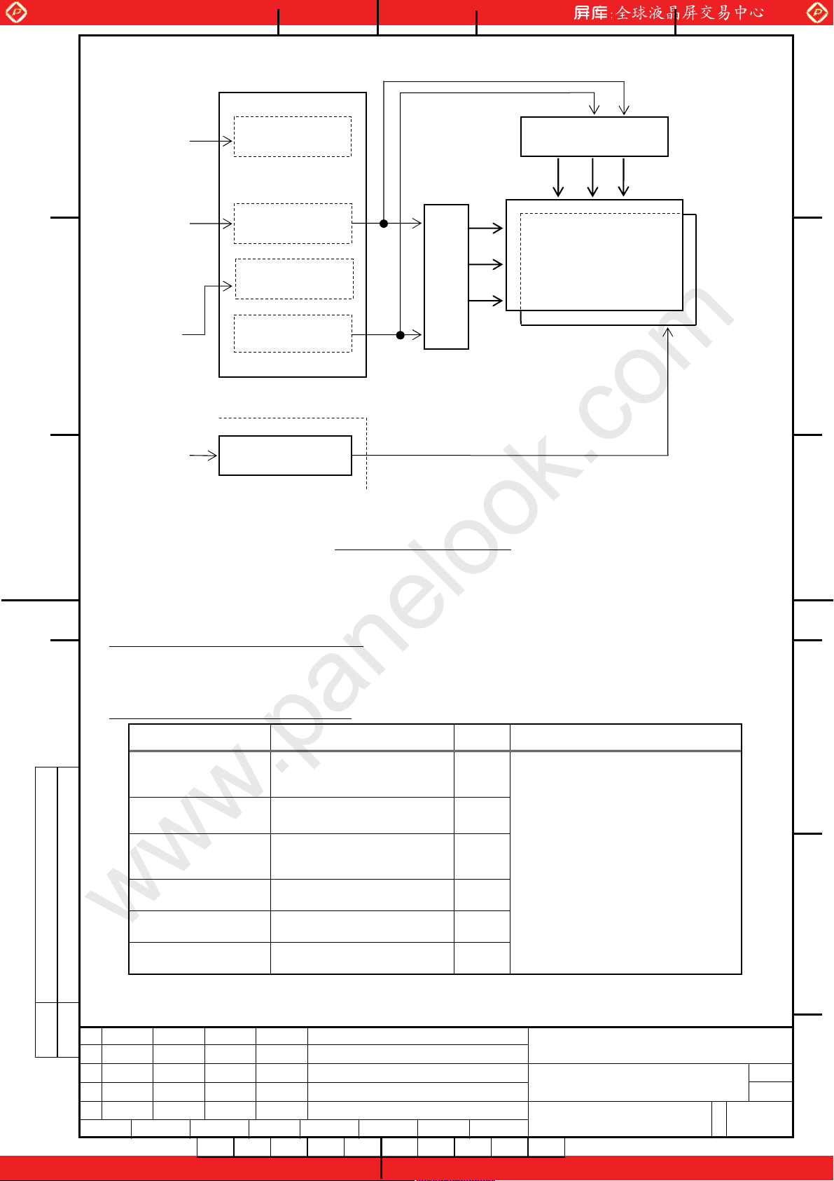
3. OVERVIEW
is LCD Module is a display unit that uses a liquid crystal panel with a TFT active
Th
matrix method with a display capacity of 1024x3(RGB)x768 dot and screen size of 38cm
(15.0 inch). This LCD module corresponds to the LVDS 1ch interface and can display 260
thousand colors. In addition, this LCD module operates under a non-interlace mode. It has
a backlight of CCFL that is built in and supplies more electric power than the exclusive
inverter places externally. The power supply of this LCD module is +3.3V DC voltage.
C C
4. CONFIGURATION
This LCD module consists of a color TFT LCD panel and a bezel where the panel driver IC
is mounted into the printed substrate, a cold-cathode florescent tube backlight, and a LVDS
interface PBC. These ar e all combined into one str ucture.
The inverter that supplies electric power to the backlight is configured separately from the
D
LCD module.
Figure 4-1 shows a block diagram of this LCD module.
D
E
ATE DOCUMENT CONTROL SECTION
D
TITLE
NA19026----C661
NA19026
NA19026
NA19026
DRAW. NO.
T
ech Bes LCD
Tech Bes LCD----00288
Tech Bes LCD Tech Bes LCD
C661
C661C661
00288
0028800288
CUST.
IT
ED
DES
DATE
IG.
DESIG. DESCRIPTION
CHECK
APPR.
CHECK
APPR.
UJITSU DISPLAY TECHNOLOGIES
F
CORPORATION
1
One step solution for LCD / PDP / OLED panel application: Datasheet, inventory and accessory!
䕣
䕘
2
䕕
䕕
/
䕤
www.panelook.com
Page 4
Global LCD Panel Exchange Center
CLKEDID
DATAEDID
A
EDID Power
Supply
RX0+
RX0-
RX1+
RX1RX2+
RX2RXC+
RXC-
EE
nterface Circuit
I
DC/
DC converter
PROM
www.panelook.com
Ga
te Driver
Da
ta Driver
TFT Color
LCD panel
1024x3(RGB)x768
B
Power
Supply
Re
ference Supply
Circuit
+3.3V DC
Separate)
(
DC
C C
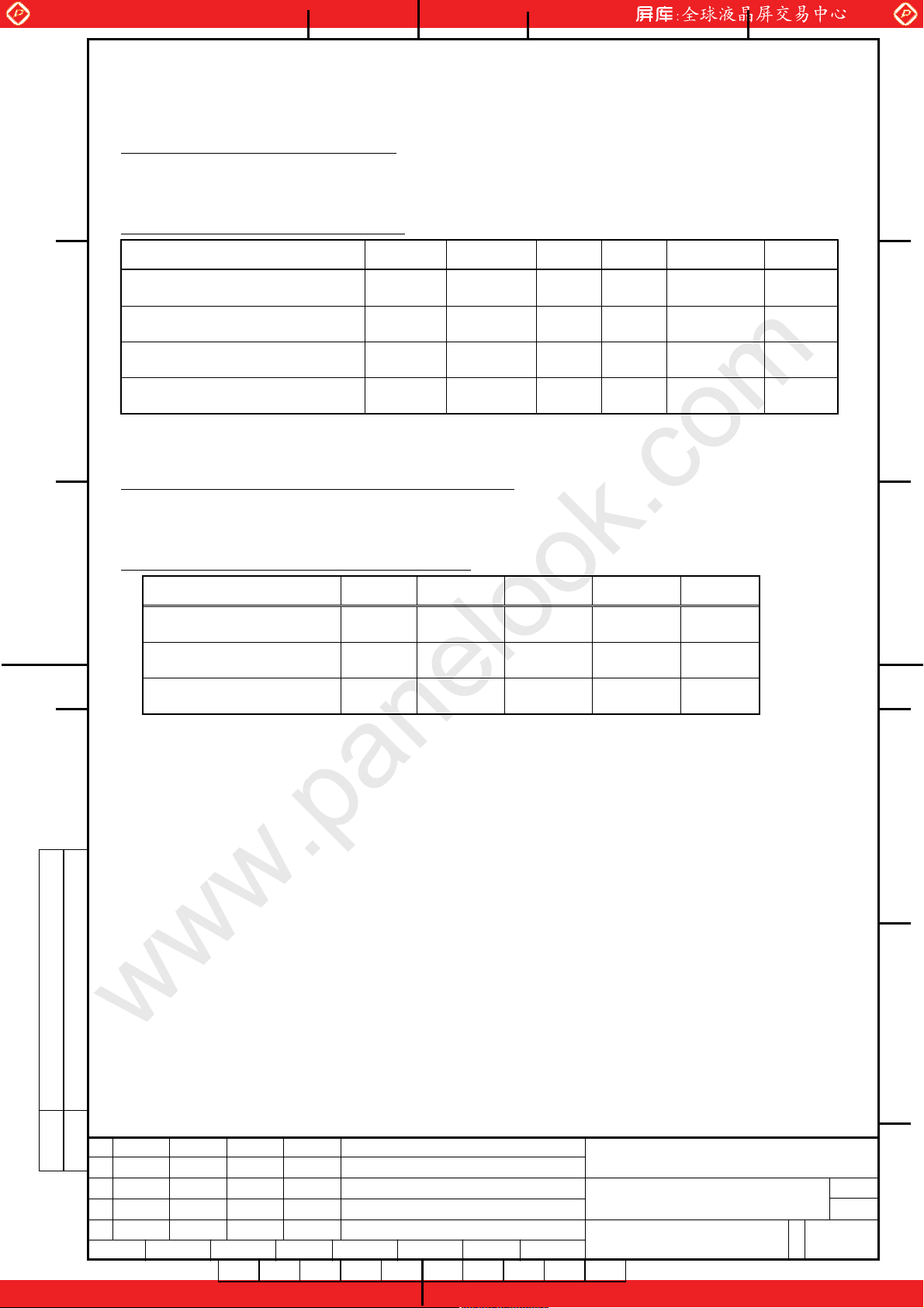
.MECHANICAL SPECIFICATIONS
5
T
able 5-1 shows the mechanical specificat ions of this LCD module.
D
Ta ble 5-1 Mechanical Sp ecifications
Invert
er Circuit
ure 4-1 Block Diagram
Fig
Back
-light
(1CCFL)
em Specifications Unit Remark
It
mensions
Di
Di
splay
Resolution
Di
splay Dot Area
(Drive range)
Dot P
itch
317.3×241.8×7.0 (max)
(1024×3)×768 㵪
304.128×228.096 mm
0.297×0.297
mm
mm
Edge type back-light is used
Inverter excluded
For details on dimension,
see dimensional outline
drawing
(on page 35,36)
P
ixel Aspect Ratio 1 : 1
㵪
Weight 670 max g
ATE DOCUMENT CONTROL SECTION
D
IT
ED
DES
DATE
IG.
DESIG. DESCRIPTION
CHECK
APPR.
CHECK
APPR.
TITLE
NA19026----C661
NA19026
NA19026
NA19026
DRAW. NO.
T
ech Bes LCD
Tech Bes LCD----00288
Tech Bes LCD Tech Bes LCD
UJITSU DISPLAY TECHNOLOGIES
F
CORPORATION
1
One step solution for LCD / PDP / OLED panel application: Datasheet, inventory and accessory!
D
E
C661
C661C661
00288
0028800288
䕣
䕘
䕕
䕕
䕤
CUST.
3
/
www.panelook.com
Page 5
Global LCD Panel Exchange Center
ABS OLUTE MAXIMUM R ATING
A
6.
T
able 6-1 shows the absolute maximum rating of this LCD module.
Table 6-1 Absolute Maximum Rating
em Symbol Condition MIN. TYP. MAX. UNIT
It
S
upply Voltage (3.3V)
www.panelook.com
CC Ta
V
=25℃
-0.3
―
4.0
V
B
Supply Voltage (EDID) V
Input Signal Voltage (L VDS)
In
put Signal Voltage (EDID) V
RECOMMEND ED OPERATIONG CONDITIONS
7.
T
able 7-1 shows the reco mmended operating con d itions
EDID
V
IN
IN
-0.3 ―Vcc+0.3
ED
-0.3
―
-0.3 V
6.25
EDID
+0
.3
V
V
V
Ta ble 7-1 Recommended Operat ing Conditions
C C
Item Symbol
Supply Voltage (3.3V)
upply Voltage (EDID) V
S
pple Voltage (V
Ri
CC
) V
V
CC
EDID
RP
MIN. TYP. MAX. UNIT
3.0 3.3 3.6
7
2.
――
―
5.5
100
V
V
䌭䌖p-
p
D
ATE DOCUMENT CONTROL SECTION
D
IT
ED
DES
DATE
IG.
DESIG. DESCRIPTION
CHECK
APPR.
CHECK
APPR.
TITLE
NA19026----C661
NA19026
NA19026
NA19026
DRAW. NO.
T
ech Bes LCD
Tech Bes LCD----00288
Tech Bes LCD Tech Bes LCD
UJITSU DISPLAY TECHNOLOGIES
F
CORPORATION
1
One step solution for LCD / PDP / OLED panel application: Datasheet, inventory and accessory!
D
E
C661
C661C661
00288
0028800288
䕣
䕘
䕕
䕕
䕤
CUST.
4
/
www.panelook.com
Page 6
Global LCD Panel Exchange Center
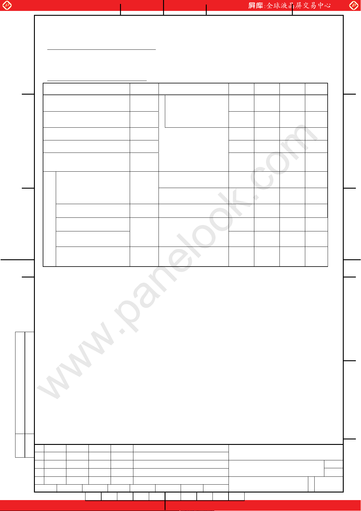
ELECTRICAL SPECIFICATIONS
8.
able 8-1 shows the electrical specifications of this LCD module. Figure 8-1 shows the
A
T
measurement circuit. Figure 8-2 s hows the equivalent circuit of the logic signal input area.
Ta ble 8-1 Electrical Specificat ions
It
em Symbol Condition MIN. TYP. MAX. Unit
D
ifferential input Voltage
(+)
ifferential input Voltage
D
(−)
ply Current
Sup
B
Supply Rush Current
pply Rush Current
Su
Duration (excess 1.2A)
FL Turn on Voltage
CC
(Note)
B
ACK LIGHT
www.panelook.com
IH ――
V
V
V
-100
――
560 850
――
――
――
Vcm=+1.2
V
IL
CC=+3.3
I
Is
V
CC ―
V
SS=0
V
Ta=25℃
CC ――
CK=54.0MHz
Ts
Frame frequency
CC
=60Hz
f
=50kHz,Ta=25℃,
V
L
S
=2
C
L
f
L=50kHz,T a=0℃,
=2
C
L
2pF
2pF
100 mV
mV
mA
2.5 A
2 ms
1650 Vrms
1700 Vrms
V
f
L
L
=50kHz,IL=6mA
L
f
L
=
V
730Vrms,I
L
=6
mA
Lighting Voltage
Lig
C C
hting Frequency 40 60 80 kHz
Recommended
Lighting Frequency
FL tube Current
(Note2)
I
L
=730Vrms
L
V
f
L=50kHz
―
50
730
―
2 6
―
Vrms
60 kHz
6.5 mA
Note)The CCFL turn on voltage is set under the appointed criteria and shall exceed the
maximum range of the specificatio n.
D
●Measurement circuit is based on Figure 8-1
D
ATE DOCUMENT CONTROL SECTION
D
IT
ED
DES
DATE
IG.
DESIG. DESCRIPTION
CHECK
APPR.
CHECK
APPR.
TITLE
NA19026----C661
NA19026
NA19026
NA19026
DRAW. NO.
T
ech Bes LCD
Tech Bes LCD----00288
Tech Bes LCD Tech Bes LCD
UJITSU DISPLAY TECHNOLOGIES
F
CORPORATION
1
One step solution for LCD / PDP / OLED panel application: Datasheet, inventory and accessory!
E
C661
C661C661
00288
0028800288
䕣
䕘
䕕
䕕
䕤
CUST.
5
/
www.panelook.com
Page 7
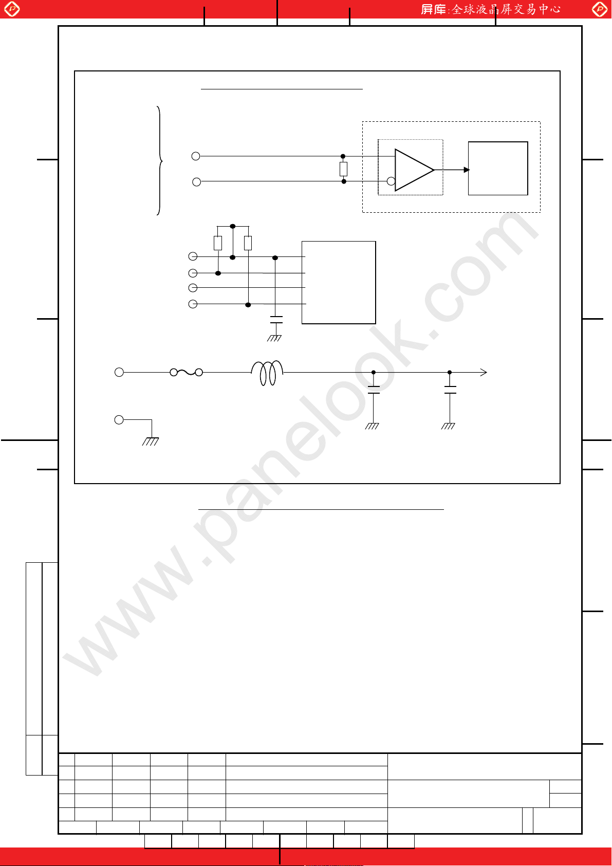
Global LCD Panel Exchange Center
p
Figure 8-1 Measurement Circuit
A
RX0+
RX0-
RX1+
RX1RX2+
RX2RXC+
RXC-
+
−
www.panelook.com
The
ifferential In
D
LVDS receiver is i ntegrated in the timing cont roller.
L
VDS Receiver
ut
100Ω
Inter
nal
Circuit
B
䌖
DA
TA
CLK
NC(5
EDID
EDID
EDID
pin)
10kΩ
10kΩ
0.1㱘F
EEPROM
WP
01-WDW6
M24C
(ST Micro) or equivalent
Internal
Vcc
C C
GN
D
Fuse
rite beads
Fer
100pF
10μF
Circuit
FG
䋨Frame Ground䋩
Fig
ure 8-2 Equivalent cir cuit of logic signal input
D
ATE DOCUMENT CONTROL SECTION
D
IT
ED
DES
DATE
IG.
DESIG. DESCRIPTION
CHECK
APPR.
CHECK
APPR.
TITLE
NA19026----C661
NA19026
NA19026
NA19026
DRAW. NO.
T
ech Bes LCD
Tech Bes LCD----00288
Tech Bes LCD Tech Bes LCD
UJITSU DISPLAY TECHNOLOGIES
F
CORPORATION
1
One step solution for LCD / PDP / OLED panel application: Datasheet, inventory and accessory!
D
E
C661
C661C661
00288
0028800288
䕣
䕘
䕕
䕕
䕤
CUST.
6
/
www.panelook.com
Page 8
Global LCD Panel Exchange Center
.. OPTICAL SPECIFICATIONS
9
able 9-1 shows the optical specifications of this LCD module.
T
A
Ta ble 9-1 Optical Specificatio ns
www.panelook.com
Item Symbol
Condition
Unit Remark Note
MIN. TYP. MAX.
Specification
sual Angle
Vi
θ
L,
R
CR≧10
Ta=25
℃
θ
U,D
Co
B
ntrast
Ratio
Response
Time (ON)
(BݲW)
CR
t
ON
θ
Ta
θ
θ
R,U,D
L,
=25℃
H
=0°
=0°
V
Response
time
(OFF)
t
OFF
θ
θ
H
=0°
=0°
V
(WݲB)
Brightness
C C
Br
ightness
Uniformity
Chromaticity
(White)
L
ΔL
x
y
θ
=0°
H
θ
V
=0°
=25℃
Ta
fL=50kHz
If=6mA
θ
U,D
θ
L,R
=0°
Ta=25
℃
=0°
=0°
80
80
250 400 ― 㵪
― 15 30 ms
――
――
de
de
Ta=0℃― 50 100 ms
Ta=25
℃
― 10 25 ms
Ta=0℃― 50 100 ms
190 300
60
――䋦
―
cd/m
0.283 0.313 0.343
299 0.329 0.359
0.
―
―
g
g
2
Top
Bottom
Left
Right
White
/
Black*1
All
white
display
*2,3,4
(1)(5)
(1)(2)
(3)(5)
(6)
(1)(3)
(5)
(1)(4)
(5)
(1)(5)
(1)(7)
Color Purity
(NTSC ratio)
LCD
Panel Type TFT Color
55 63 ―
䋦
(1)(5)
D
D
isplay Mode Normally Black
D
W
ide Viewing Angle Technology MVA
timum Viewing Angle Symmetry
Op
Display Color 262,144 (6 bit color)
Co
lor of non-display area Black
rface Treatme nt
Su
Glare
Low reflection 䋲H
E
ATE DOCUMENT CONTROL SECTION
D
TITLE
NA19026----C661
NA19026
NA19026
NA19026
DRAW. NO.
T
ech Bes LCD
Tech Bes LCD----00288
Tech Bes LCD Tech Bes LCD
C661
C661C661
00288
0028800288
CUST.
IT
ED
DES
DATE
IG.
DESIG. DESCRIPTION
CHECK
APPR.
CHECK
APPR.
UJITSU DISPLAY TECHNOLOGIES
F
CORPORATION
1
One step solution for LCD / PDP / OLED panel application: Datasheet, inventory and accessory!
䕣
䕘
7
䕕
䕕
/
䕤
www.panelook.com
Page 9

Global LCD Panel Exchange Center
Note
*1) Brightness, Chromaticity, Contrast is measured at a spot diameter ofφ2 and a distance=500mm.
A
*2) The value is measured 15-20 minutes after the light on.
*3) The power supply condition is VCC=3.3V,fL=50kHz,If=6mA when the optical
specification is mea sured.
*4) The operation life of the C CFL is limited. The brightness will deteriorate over time.
B
www.panelook.com
C C
D
D
E
ATE DOCUMENT CONTROL SECTION
D
IT
ED
DES
DATE
IG.
DESIG. DESCRIPTION
CHECK
APPR.
CHECK
APPR.
TITLE
NA19026----C661
NA19026
NA19026
NA19026
DRAW. NO.
T
ech Bes LCD
Tech Bes LCD----00288
Tech Bes LCD Tech Bes LCD
UJITSU DISPLAY TECHNOLOGIES
F
CORPORATION
1
One step solution for LCD / PDP / OLED panel application: Datasheet, inventory and accessory!
C661
C661C661
00288
0028800288
䕣
䕘
䕕
䕕
䕤
CUST.
8
/
www.panelook.com
Page 10
Global LCD Panel Exchange Center
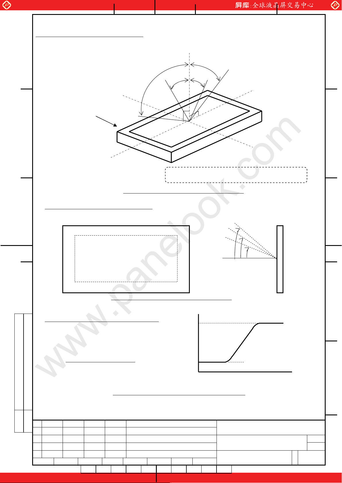
play
www.panelook.com
Note 1) D
A
B
efinition of Viewing Angle (1)
sed on Figure 9-1.
Ba
T
Le
Y+
op (12 o’clock Direction)
LCD module
X-
ft (9 o’clock Direction)
Figure 9-1 Definition of Viewing Angle (1)
㱔
䌌
㱔
U
䋪㸢 㱔
*0㫦(Fro
U
nt)
㱔
䌒
㱔
䌄
䋽䋰㫦䋬㱔D䋽䋰
X+
Ri
ght (3 o’clock Direction)
Y-
Bottom (6 o’clock Direction)
㫦䋬㱔
䋽䋰
L
㫦䋬㱔
R
䋽䋰
㫦
Note 2) D
C C
efinition of Viewing Angle (2)
Based on Figure 9-2.
Di
splay Surface
㱔
㱔
L,R,U,D
=0㫦
㱔
MIN
TYP
㱔
MAX
s
Di
Surfa
ce
D
Figure 9-2 Definition of Viewing Angle (2)
Note 3) Definition of Contrast Ratio (CR)
L
W
White
Determined by Formula (1) based on
Figure 9-3 Voltage-Brightness
ightness
characteristics.
Br
䌛L䌝
ack
0
Bl
anel Drive Voltage 䌛䌖䌝
P
䌌
Brightness at white)
(
W
=
䌌
(Brightness at black) 㵺㵺(1)
䌂
L
B
0
D
E
Figure 9-3 Voltage-Brightness Characteristics
ATE DOCUMENT CONTROL SECTION
D
IT
ED
DES
DATE
IG.
DESIG. DESCRIPTION
CHECK
APPR.
CHECK
APPR.
TITLE
NA19026----C661
NA19026
NA19026
NA19026
DRAW. NO.
T
ech Bes LCD
Tech Bes LCD----00288
Tech Bes LCD Tech Bes LCD
UJITSU DISPLAY TECHNOLOGIES
F
CORPORATION
1
One step solution for LCD / PDP / OLED panel application: Datasheet, inventory and accessory!
C661
C661C661
00288
0028800288
䕣
䕘
䕕
䕕
䕤
CUST.
9
/
www.panelook.com
Page 11
Global LCD Panel Exchange Center
p
p
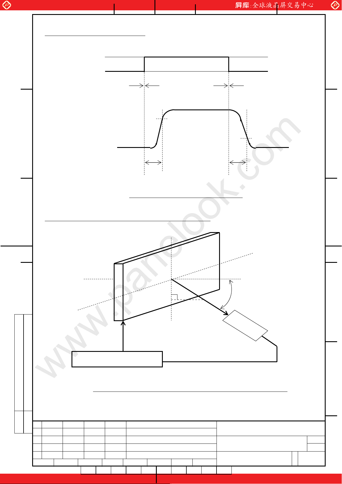
Note 4) Definition of Response Time
Based on Figure 9-4.
www.panelook.com
A
D
rive signal of
LCD panel
ON
OFF
Non-select status Select status Non-select status
100%
lative
Re
Brightnes
B
90%
White
10%
0%
Bl
ack
ON
Res
䌴
on
on
se Time O FF Res
䌴
f
of
on
se Time
Bl
ack
Figure 9-4 Definition of Response Time
C C
e 5) Contrast Ratio and Response Measurement System
Not
D
Ba
sed on Figure 9-5.
-
Z
-
X
rive and Measurement System
D
Figure 9-5 Contrast Ratio and Response T ime Measurement System
+
Y
+
X
+
Z
ightness Meter or
Br
㱔
-
Y
Luminance colorimeter
(with luminosity
correction function)
D
E
ATE DOCUMENT CONTROL SECTION
D
IT
ED
DES
DATE
IG.
DESIG. DESCRIPTION
CHECK
APPR.
CHECK
APPR.
TITLE
NA19026----C661
NA19026
NA19026
NA19026
DRAW. NO.
T
ech Bes LCD
Tech Bes LCD----00288
Tech Bes LCD Tech Bes LCD
UJITSU DISPLAY TECHNOLOGIES
F
CORPORATION
1
One step solution for LCD / PDP / OLED panel application: Datasheet, inventory and accessory!
C661
C661C661
00288
0028800288
䕣
䕘
䕕
䕕
䕤
CUST.
10
/
www.panelook.com
Page 12
Global LCD Panel Exchange Center
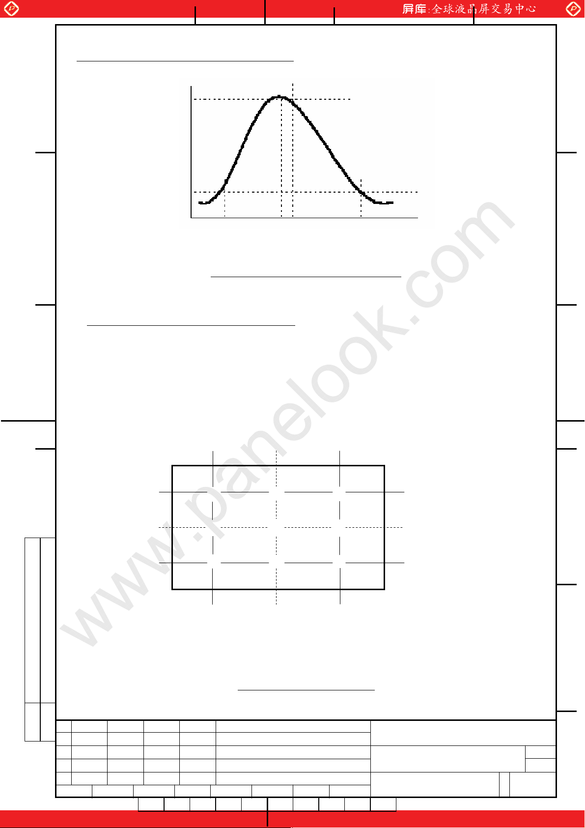
Note 6) Definition of Optimum Viewing Angle
www.panelook.com
Co
MAX
ntrast
A
Ratio
10
B
䋨-䋩
V
6 o’cloc
e 7) Definition of Brightness Uniformity
Not
Brightness Uniformi ty is defined by the following formula using 9 points 䋨㽲䌾㽺䋩
The
k㸠
Fig
ure 9-6 Definition of Viewing Angle
0
iewing Angle㱔
䋨+䋩
㸢12 o’clock
of the brightness measur ing value shown bellow.
C C
D
Definitional Equat ion:
䌻䋨Minimum Brightness of 㽲䌾㽺䋩䋯䋨Maximum Brightness of 㽲䌾㽺䋩䌽㬍䋱䋰䋰䌛䋦䌝
154 512
①
②
③
④
⑤
⑥
870
⑦
⑧
⑨
Do
t
115
384
653
Note) The center of each position is defined by th e center spot position of the
brightness meter in which the tolerance of the measurement position is ±3mm.
D
E
Figure 9-7 Measuring Points
ATE DOCUMENT CONTROL SECTION
D
IT
ED
DES
DATE
IG.
DESIG. DESCRIPTION
CHECK
APPR.
CHECK
APPR.
TITLE
NA19026----C661
NA19026
NA19026
NA19026
DRAW. NO.
T
ech Bes LCD
Tech Bes LCD----00288
Tech Bes LCD Tech Bes LCD
UJITSU DISPLAY TECHNOLOGIES
F
CORPORATION
1
One step solution for LCD / PDP / OLED panel application: Datasheet, inventory and accessory!
C661
C661C661
00288
0028800288
䕣
䕘
䕕
䕕
䕤
CUST.
11
/
www.panelook.com
Page 13

Global LCD Panel Exchange Center
0. INTERFACE SPECIFICATIONS
1
1 Interface Signal Alignme nt
A
10.
T
able 10-1 shows the descri ption and configuration of the interface signals (CN1)
Pi
www.panelook.com
Ta ble 10-1 Interface signals
n No. Symbol Function
+3.3V power supply
+3.3V power supply
B
1 V
2 V
VSS Ground
3
VSS Ground
4
5
CC
CC
RX0- LVDS signal 0-
6 RX0+ LVDS signal 0+
VSS Ground
7
8 RX1- LVDS signal 19
C C
10 VSS Ground
RX1+ LVDS signal 1+
11 RX2- LVDS signal 212
RX2+ LVDS signal 2+
13 VSS Ground
14 RX
15 RX
C- LVDS signal CLK-
C+ LVDS signal CLK+
D
16 VS
17 VEDID
8 NC NC
1
S Ground
19 CLKEDID DDC
20 D
Co
nnector used :FI-SEB20P-HF13
ATA
EDID DDC
Adapted Connector:FI-SE20M
Name of Maker:Japan A viation Electronics Ltd.
Note) Terminal 18 should be open.
ATE DOCUMENT CONTROL SECTION
D
DDC+3.
clock
data
3Vpower supply
TITLE
NA19026----C661
NA19026
NA19026
DRAW. NO.
T
Tech Bes LCD----00288
Tech Bes LCD Tech Bes LCD
NA19026
ech Bes LCD
D
E
C661
C661C661
00288
0028800288
CUST.
IT
ED
DES
DATE
IG.
DESIG. DESCRIPTION
CHECK
APPR.
CHECK
APPR.
UJITSU DISPLAY TECHNOLOGIES
F
CORPORATION
1
One step solution for LCD / PDP / OLED panel application: Datasheet, inventory and accessory!
䕣
䕘
12
䕕
䕕
/
䕤
www.panelook.com
Page 14

Global LCD Panel Exchange Center
T
ransmitter
DS90C365
pin INPUT System side
44
45
47
48
1
3
4
A
B
ut
Inp
Signal
*1
R0
R1
R2
R3
R4
R5
G0
T
TxIN0
TxIN1
TxIN2
TxIN3
TxIN4
TxIN5
TxIN6
www.panelook.com
able 10-2 LVDS Data A ssignment
Interface connector
LCD module
pin
UT0+
Tx O
Tx OUT0-
6
5
Rx0+
Rx0-
LCD
Control
input
R0
R1
R2
R3
R4
R5
G0
G1
G2
G3
G4
G5
B0
B1
6
7
9
10
12
13
15
TxIN7
TxIN8
TxIN9
TxIN10
TxIN11
TxIN12
TxIN13
Tx O
UT1+
Tx OUT1-
9
8
Rx1+
Rx1-
G1
G2
G3
G4
G5
B0
B1
C C
B2
B3
B4
B5
RSVD
RSVD
ENAB
16
18
19
20
22
23
25
TxIN14
TxIN15
TxIN16
TxIN17
TxIN18
TxIN19
TxIN20
Tx OUT2+
Tx OUT2-
12
11
Rx2+
Rx2-
B2
B3
B4
B5
Not use
Not use
ENAB
D
D
CLK 26 TxCLK IN
TxCLK OUT+
15
RxC+
DCLK
D
TxCLK OUT-
*1 Th
e RSVD (reserved) pin on the tran smitter should be connected to the Ground
ATE DOCUMENT CONTROL SECTION
D
IT
ED
DES
DATE
IG.
DESIG. DESCRIPTION
CHECK
APPR.
CHECK
APPR.
14
RxC-
TITLE
NA19026----C661
NA19026
NA19026
NA19026
DRAW. NO.
T
ech Bes LCD
Tech Bes LCD----00288
Tech Bes LCD Tech Bes LCD
UJITSU DISPLAY TECHNOLOGIES
F
CORPORATION
1
One step solution for LCD / PDP / OLED panel application: Datasheet, inventory and accessory!
E
C661
C661C661
00288
0028800288
䕣
䕘
䕕
䕕
䕤
CUST.
13
/
www.panelook.com
Page 15

Global LCD Panel Exchange Center
0.2 CORRESPONDENCE BETWEEN COLOR AND INPUT SIGNAL
1
able 10-3 shows the cor respondence between input signal and color
T
lor and
Co
A
Brightness
Gradation
Black
Blue
Green
Cyan
Re
d
䌣 䌃䌯䌬䌯䌲
enta
Mag
B
䌂䌡䌳䌩
Y
ellow
White
Black 0
×
1
Darker 2
×
:
Ø
䌤 Gradation
䌒䌥
C C
hter 61
Brig
Ø
d 63
Re
Black 0
×
rker
Da
::
:
:
:
::
62
1
2
×
:
Ø
䌥䌥䌮 Gradation
Brighte
䌇䌲
Ø
Green
:
::
::::
r 61
62
63
Black 0
D
×
Da
rker 2
1
×
:
Ø
䌥 Gradation
::
:
:
::
:
Brighter 61
䌂䌬䌵
Ø
Blu
e 63
62
R4 R3 R2 R1 R0
R5
0
0 0 0 0 0 0 0 0 0 0 0 0 0 0 0 0 0
0 0 0 0 0 0 0 0 0 0 0 1 1 1 1 1 1
0
0
0 0 0 0 0
0 0 0 0 0
0
1 1 1 1 1 0 0 0 0 0 0 0 0 0 0 0 0
1
1
1 1 1 1 1
1 1 1 1 1
1
1 1 1 1 1
1
0 0 0 0 0 0 0 0 0 0 0 0 0 0 0 0 0
0
0 0 0 0 1 0 0 0 0 0 0 0 0 0 0 0 0
0
0 0 0 0 1 0 0 0 0 0 0 0 0 0 0 0 0 0
:
: : : : : : :
: : : : : : : : : : : : : : : :
: : : : : : : : : : : : : : : :
: : : : : : : :
: : : : : : : : : : : : : : : :
: : : : : : : : : : : : : : : :
: : : : : : : :
: : : : : : : : : : : : : : : :
: : : : : : : : : : : : : : : :
1 1 1 0 1
1
1
1 1 1 1 0
1 1 1 1 1
1
0
0 0 0 0 0
0 0 0 0 0
0
0 0 0 0 0
0
:
: : : : : : :
: : : : : : : : : : : : : : : :
: : : : : : : : : : : : : : : :
: : : : : : : :
: : : : : : : : : : : : : : : :
: : : : : : : : : : : : : : : :
: : : : : : : :
: : : : : : : : : : : : : : : :
: : : : : : : : : : : : : : : :
0
0 0 0 0 0
0 0 0 0 0
0
0
0 0 0 0 0
0 0 0 0 0
0
0
0 0 0 0 0
0
0 0 0 0 0
: : : : : : :
: : : : : : : : : : : : : : : :
:
: : : : : : : :: : : : : : : :
:
: : : : : : :
: : : : : : : : : : : : : : : :
: : : : : : : : : : : : : : : :
: : : : : : :
: : : : : : : : : : : : : : : :
:
: : : : : : : : : : : : : : : :
0 0 0 0 0
0
0 0 0 0 0
0
0
0 0 0 0 0
www.panelook.com
Data Signal (0:Low Level, 1:High Level)
G5 G4 G3
1 1 1 1 1 1
1 1 1 1 1 1
0
1
1
: : : : : : : : : : : : :
: : : : : : : : : : : : : : : :
: : : : : : : : : : : : : : : :
: : : : : : : : : : : : : : : :
: : : : : : : : : : : : : : : :
: : : : : : : : : : : : : : : :
0
0
0
0
0
0
: : : : : : : : : : : : : : : :
: : : : : : : : : : : : : : : :
: : : : : : : : : : : : : : : :
: : : : : : : : : : : : : : : :
: : : : : : : : : : : : :
: : : : : : : : : : : : : : : :
1
1
1
0
0
0
: : : : : : : : : : : : : : : :
: : : : : : : :: : : : : : : :
: : : : : : : : : : : : :
: : : : : : : : : : : : : : : :
: : : : : : : : : : : : : : : :
: : : : : : : : : : : : : : : :
0
0
0
G2 G1 G0 B5 B4 B3 B2 B1 B0
0
1
0 0 0 0 0 1 1 1 1 1 1
1 1 1 1 1
1 1 1 1 1
0 0 0 0 0
0 0 0 0 0
0 0 0 0 0
0 0 0 0 0
0 0 0 0 1
0 0 0 1 0
1 1 1 0 1
1 1 1 1 0
1 1 1 1 1
0 0 0 0 0
0 0 0 0 0
0 0 0 0 0
0 0 0 0 0
0 0 0 0 0
0 0 0 0 0
0
1
: : : : : : : :
: : : : : : : : : :
: : : : : : : :
: : : : : : : : : : : : : : : :
: : : : : : : :
: : : : : : : : : : : : : : : :
0
0
0
0 0 0 0 0 0
0 0 0 0 0 0
0
: : : : : : : :
: : : : : : : : : : : : : : : :
: : : : : : : :
: : : : : : : : : : : : : : : :
: : : : : : : :
: : : : : : : : : :
0
0
0
0
0
0
: : : : : : : :
: : : : : : : :: : : : : : : :
: : : : : : : :
: : : : : : : : : :
: : : : : : : :
: : : : : : : : : : : : : : : :
1
1
1
0 0 0 0 0
1 1 1 1 1
0 0 0 0 0
1 1 1 1 1
: : :
: : : : : :
0 0 0 0 0
0 0 0 0 0
0 0 0 0 0
0 0 0 0 0
: : :
: : : : : :
0 0 0 0 0
0 0 0 0 0
0 0 0 0 0
0 0 0 0 0
0 0 0 0 1
0 0 0 1 0
: : :
: : : : : :
1 1 1 0 1
1 1 1 1 0
1 1 1 1 1
D
Note 1) D
efinition of gray scale: Color (n)…”n” indicates the gray scale level.
The larger number means brighter level.
Note 2) Data: 1:High level, 0:Low level
Note 3) There are 18 color data which consists of 6 bit of red, green and blue where they
individually display 64 signals. By combining these colors, 262,144 colors can be
displayed.
ATE DOCUMENT CONTROL SECTION
D
IT
ED
DES
DATE
IG.
DESIG. DESCRIPTION
CHECK
APPR.
CHECK
APPR.
TITLE
NA19026----C661
NA19026
NA19026
NA19026
DRAW. NO.
T
ech Bes LCD
Tech Bes LCD----00288
Tech Bes LCD Tech Bes LCD
UJITSU DISPLAY TECHNOLOGIES
F
CORPORATION
1
One step solution for LCD / PDP / OLED panel application: Datasheet, inventory and accessory!
E
C661
C661C661
00288
0028800288
䕣
䕘
䕕
䕕
䕤
CUST.
14
/
www.panelook.com
Page 16

Global LCD Panel Exchange Center
3 INPUT SIGNAL TIMING
10.
input signal timing is show n i n table 10-3 and figure 10-1.
A
The
www.panelook.com
Ta ble 10-3 T im ing Chara cterist ics
(Ta=0〜50℃,Vcc=3.3±0.3V)
Item Symbol MIN. TYP. MAX. Unit Remark
Period
DC
LK
Signal
(Clock)
B
CLK-Data
D
Timing
zontal
Hori
Signal
rtical
Ve
Signal
C C
AB signal Data ENAB timing
EN
Frequency
Duty
High time
Low time
Setup time
Hold time
Horizontal period
Hor. Period (1)
Hor. Display period
Vertical Period
Ver. Frequency
Ver. Display period
Tc
1/Tc
Tch/Tc
TclkH
TclkL
Ts
et
Thold
Th
Th
Thd
Tv
1/Tv
Tvd
Td
n
15
15.
60
45
6.0
6.0
3
5
1320
0
18.
1024
780
55
768
─
15.38
65
50
─
─
─
─
1344
20.68
1024
806
60
768
0
16.67
66
55
─
─
─
─
2046
─
1024
1023
65
768
─
ns
MHz
%
ns
ns
ns
ns
DCL
K
μs
DCL
K
Th
Hz
Th
DCL
K
*4
*1,4
*4
*2
*1
16.67ms
*2
*3
*1) ・The horizontal direction of the dis pl ay p os ition is defined by the rise of the ENA B s ign al.
Right after the signal rises, the latched data is displayed from the left edge of the screen.
The vertical direction of the display position is when th e E N AB signal changes from “H”
to “L” and “L” is over 2048 DCLK, then the next risen ENAB signal data is displayed from
the top line of the screen.
D
*2) ・If the “H” period of the ENAB signal is less then 1024 DCLK, then black is displayed on the
remaining area.
・If the ENAB signal is les s than 768 Th within a frame, then the d is pl ayed data is
continuously displaye d from the top line of the screen co ntinuously.
*3) ・If the valid data period an d the “H” p eriod of the ENAB signal do not synchronize, then
the display position is displayed as out of place.
*
4) When the horizontal period is less than 1320 DCLK or 18μs, the display quality such as
unevenness and light line defect can occur.
If the DCLK frequency exceeds 66MHz, garbled data may ca use flickering.
In addition, if the DCLK frequency is le ss than 60MHz, then unevenness may occur.
D
E
ATE DOCUMENT CONTROL SECTION
D
IT
ED
DES
DATE
IG.
DESIG. DESCRIPTION
CHECK
APPR.
CHECK
APPR.
TITLE
NA19026----C661
NA19026
NA19026
NA19026
DRAW. NO.
T
ech Bes LCD
Tech Bes LCD----00288
Tech Bes LCD Tech Bes LCD
UJITSU DISPLAY TECHNOLOGIES
F
CORPORATION
1
One step solution for LCD / PDP / OLED panel application: Datasheet, inventory and accessory!
C661
C661C661
00288
0028800288
䕣
䕘
䕕
䕕
䕤
CUST.
15
/
www.panelook.com
Page 17

Global LCD Panel Exchange Center
A
DCLK
ENAB
R5-0
G5-0
B5-0
B
R5-0
G5-0
B5-0
ENAB
www.panelook.com
Tc
lk
TclkL
0.9V
1Tset
Tc
Tc
2.3V
Tc
1.
65
h
Th
Thd
old
2.3V
0.9V
Th
R5-0
C0
01 C768
G5-0
B5-0
C C
ENAB
Tvd
Tv
Tc
DCLK
D
R5-0
0001
0002
0003
0004
0005
0006 1018
1019
1021 1023
1020
1022
1024
G5-0
B5-0
Tdn Tdn
ENAB
D
Figure 10-1 Input Signal Timing Chart
ATE DOCUMENT CONTROL SECTION
D
IT
ED
DES
DATE
IG.
DESIG. DESCRIPTION
CHECK
APPR.
CHECK
APPR.
TITLE
NA19026----C661
NA19026
NA19026
NA19026
DRAW. NO.
T
ech Bes LCD
Tech Bes LCD----00288
Tech Bes LCD Tech Bes LCD
UJITSU DISPLAY TECHNOLOGIES
F
CORPORATION
1
One step solution for LCD / PDP / OLED panel application: Datasheet, inventory and accessory!
E
C661
C661C661
00288
0028800288
䕣
䕘
䕕
䕕
䕤
CUST.
16
/
www.panelook.com
Page 18

Global LCD Panel Exchange Center
㻡
4 Correspondence bet ween Data and Display Position
10.
ure 10-2 shows the Correspondence between D ata and Display Positio n.
A
Fig
S0001 S0002 S0003 S0004 S0005 S0006 S0007 S0008 S3071 S3072
www.panelook.com
C001
R
0001G0001B0001R0002G0002B0002R0003G0003
G
1024B1024
B
G
C7
68R0001G0001B0001R0002G0002B0002R0003G0003
igure 10-2 Correspondence Data and Display Position
F
1024B1024
C C
10-5 Pow
er Supply Sequence
ure 10-3 defines the rise tim e of the power supply, voltage descent and the
Fig
power supply sequence. Especially the sequence of power supply and the input
signal is necessary to latch up of the driver IC and DC driving.
D
Power Supply Voltage
Vcc
O
ON
FF
(0V)
LVDS
Input Signal
ATE DOCUMENT CONTROL SECTION
D
H
L
3.0V
T4㻡20ms
90%
10%
T1
T2
10ms㻡T1㻡40m
10ms㻡T2㻡40ms
Figure 10-3 Power Supply Sequence
T5㻡20m
亖
3.0V
2.5V
s
s(Voltage Descent)
亖
亖
亖
TITLE
DRAW. NO.
3.
0V
3.0V
0.5V
ms
C661
C661C661
00288
0028800288
T6
0.1s
0ms㻡T3㻡40
NA19026----C661
NA19026
NA19026
NA19026
T
ech Bes LCD
Tech Bes LCD----00288
Tech Bes LCD Tech Bes LCD
D
E
CUST.
IT
ED
DES
DATE
IG.
DESIG. DESCRIPTION
CHECK
APPR.
CHECK
APPR.
UJITSU DISPLAY TECHNOLOGIES
F
CORPORATION
1
One step solution for LCD / PDP / OLED panel application: Datasheet, inventory and accessory!
䕣
䕘
17
䕕
䕕
/
䕤
www.panelook.com
Page 19

Global LCD Panel Exchange Center
6 EDID Signal Timing
10.
able 10-4 shows DC characteristics of EDID signals. Figure 10-4 shows in put ti ming.
T
www.panelook.com
㪘
SC
Ta ble 10-5 shows AC characteristics and Table 10-6 shows the contents of EDID data.
L,SDA
Ta ble 10-4 EDID DC Characteristics
Item Symbol MIN. MAX.
Hi
gh voltage
VIH
0.
7V
EDID
─
䋨䌔a䋽䋰䌾䋵䋰㷄䋬䌖cc䋽3.3㫧䋰䋮3䌖䋩
Uni
t
Re
marks
V
Terminal
input
voltage
Low voltage
VIL
─
0.
3V
EDID
V
㪙
Hysteresis voltage
Ou
tput voltage
ll
Input
leak
current
A
input-and-output
pins
WP pin
Output leak current
VHY
VOL1
VOL2
Tv
1/Tv
n
Td
S
0.05V
─
─
-10
-10
-10
EDID
─
4
0.
0.6
10
50
10
V
V
V
μA
μA
μA
I0L
=3mA, V
I0L=6mA, V
EDID
EDID
VIN=0.1V to V
WP= V
VOUT=0
D
EDI
.1V to V
=2.5V
=2.5
EDI
D
EDID
V
,W
P=VSS
㪚 㪚
Terminal capacity
(Input and output)
erating current
Op
tillness current
S
Cin,Co
ICC W
ICC Re
ICCS
ut
r
─
─
─
─
─
10
3
1
30
100
pF
mA
mA
μA
μA
VCC=5
Ta=25㷄, Fclk=1MHz
V
V
V
VCC=5.5V,SDA=SCL=VCC
WP=VSS,A0,A㪈,A2=VSS
.0V
=
5.5V,SCL=400KHz
EDID
=
5.5V,SCL=400KHz
EDID
CC=3.0V,SDA=SCL=VCC
㪛
ATE DOCUMENT CONTROL SECTION
D
IT
ED
DES
DATE
IG.
DESIG. DESCRIPTION
CHECK
APPR.
CHECK
APPR.
TITLE
NA19026----C661
NA19026
NA19026
NA19026
DRAW. NO.
T
ech Bes LCD
Tech Bes LCD----00288
Tech Bes LCD Tech Bes LCD
UJITSU DISPLAY TECHNOLOGIES
F
CORPORATION
㪈
One step solution for LCD / PDP / OLED panel application: Datasheet, inventory and accessory!
㪛
㪜
C661
C661C661
00288
0028800288
䕣
䕘
䕕
䕕
䕤
CUST.
18
/
www.panelook.com
Page 20

Global LCD Panel Exchange Center
able 10-5 EDID AC Characteristics
T
www.panelook.com
㪘
Item Symbol
Standard
operation mode
Vcc=2.5V-5.5V
Vcc=4.5V-5.5V
High-speed
operation mode
Unit Remarks
MIN. MAX. MIN. MAX.
lock frequency Fclk
C
THI
lock high time
C
ock low time TLOW
Cl
SDA
, SCL rising time TR
, SCL falling time TF
SDA
㪙
ST
ART hold time
ART setup time
ST
DATA input hold time
DATA input setup time
OP setup time
ST
Output decision time
from a clock
B
us free time TBUF
Min
㪚 㪚
imum VIH, VIL
Rising time
Spike oppression
(SDA, SCL pins)
write-in cycle time TWR
A
The
number of times of
data rewriting
GH
D:SDA
TH
TSU:ST
THD:
DAT
DAT
STU:
TSU:STO
TAA 100
TOF
TSP
─
─
4000
4700
─
─
4000
A
4700
0
250
4700
4700
─
─
─
1M
100
─
─
1000
300
─
─
─
─
─
3500
─
250
50
10
─
20+
─
600
1300
─
─
600
600
0
100
600
100
1300
0.1CB
─
─
1M
400
─
─
300
300
─
─
─
─
─
900
─
250
50
10
─
kHz
ns
ns
ns
ns
ns
ns
ns
ns
ns
ns
ns
ns
ns
ms
cycle
CB≦10
Byt
25℃,
0pF
e and page mode
Vcc=5.0V
block mode
ATE DOCUMENT CONTROL SECTION
D
㪛
CLKedid
TSU:STA
TAedid
DA
SOA
OUT
TAA
TF
TH
IGH
TLOW
THD:
STA THD:DAT
TH
D:STA
Fig
ure 10-4 EDID signal timi ng
TSU:DA
T
AA
TR
㪛
T
TSU:STA
TBUF
㪜
TITLE
NA19026----C661
NA19026
NA19026
DRAW. NO.
T
Tech Bes LCD----00288
Tech Bes LCD Tech Bes LCD
NA19026
ech Bes LCD
C661
C661C661
00288
0028800288
CUST.
IT
ED
DES
DATE
IG.
DESIG. DESCRIPTION
CHECK
APPR.
CHECK
APPR.
UJITSU DISPLAY TECHNOLOGIES
F
CORPORATION
㪈
One step solution for LCD / PDP / OLED panel application: Datasheet, inventory and accessory!
䕣
䕘
19
䕕
䕕
/
䕤
www.panelook.com
Page 21

Global LCD Panel Exchange Center
.
Ad
ress
㪘
Byte
s
Header (8bytes) Color Characteristics (10bytes)
No
d
scription Data Addr
De
www.panelook.com
able 10-6 The Content s of EDID data
T
No
ess
Byte
s
.
scription Data
De
00h 1
01h
1 FFh 1Ah 1 Blue/White Low Bits **h
02h 1
00h 19h 1 Red/Green Low Bits **h
FFh 1Bh 1 Red-x **h
03h 1 FFh 1Ch 1 Red-y **h
04h 1
FFh 1Dh 1 Green-x **h
05h 1 FFh 1Eh 1 Green-y **h
㪙
06h 1 FFh 1Fh 1 Blue-x **h
07h 1
V
endor/Product identification (10 bytes) 21h 1 White-x **h
08h
2 ID Manufacturer name 1894h 22h 1 White-y **h
00h 20h 1 Blue-y **h
0Ah 2 ID product code ****h Established timing (3 bytes)
0C
h 1 ID serial number **h 23h 1 Established Timings1 00h
h 1 ID serial number **h 24h 1 Established Timings2 00h
0D
M
h 1 ID serial number **h 25h 1
㪚 㪚
0E
h 1 ID serial number **h Standard timing identification
0F
anufactures reserved
timing
00h
(16 bytes)
10h
1
12h 1
1 Week of man ufacture
**䌨
1h 1 Y ear of manufacture **h
ID (2bytes)
ED
Version # 01h
26h 2 Standard timing
Identification #1
28h 2 Standard timing
Identification #2
61h
40h
01h
01h
13h 1 Revision # 03h
asic display parameter/features (5 bytes)
㪛
B
14h 1
15h
16h
1 Max. horizontal image size 1Eh
1 Max. vertical image size 17h
17h 1
Video input definition 80h
Display transfer
B4h
2Ah 2 Standard timing
Identification #3
2Ch 2 Standard timing
Identification #4
2Eh 2 Standard timing
Identification #5
01h
01h
01h
01h
01h
01h
㪛
Characteristics (Gamma)
18h 1
ATE DOCUMENT CONTROL SECTION
D
Feature support 08h
30h 2
Standard timing
Identification #6
32h 2 Standard timing
Identification #7
34h 2 Standard timing
Identification #8
TITLE
NA19026----C661
NA19026
NA19026
DRAW. NO.
T
Tech Bes LCD----00288
Tech Bes LCD Tech Bes LCD
NA19026
ech Bes LCD
C661
C661C661
00288
0028800288
01h
01h
01h
01h
01h
01h
㪜
CUST.
IT
ED
DES
DATE
IG.
DESIG. DESCRIPTION
CHECK
APPR.
CHECK
APPR.
UJITSU DISPLAY TECHNOLOGIES
F
CORPORATION
㪈
One step solution for LCD / PDP / OLED panel application: Datasheet, inventory and accessory!
䕣
䕘
20
䕕
䕕
/
䕤
www.panelook.com
Page 22

Global LCD Panel Exchange Center
dd
A
ress
㪘
D
D
No.
bytes
etailed timing descript ion (72 bytes) 56h 00h
etailed timing descript ion 1 (18 bytes) 57h 00h
Description Data Add
36h
37h
38h
00h Detailed timing description #3 or monitor
39h
h 41h 5Bh 00h
3A
3B
h 00h 5Ch 00h
㪙
h 25h 5Dh 10h
3C
3Dh 30h 5Eh 00h
3Eh 00h 5Fh 00h
h 00h 60h 00h
3F
www.panelook.com
No.
ress
bytes
64h 58h 00h
19h 59h 00h
Descriptor (18 bytes)
40h 5Ah 00h
Description Data
40h
41h
42h
43h
44h 10h 65h 00h
㪚 㪚
45h
46h
47h
Detai
led timing description #2 or monitor
00h 61h 00h
00h 62h 00h
30h 63h 00h
E4h 64h 00h
00h 66h 00h
00h 67h 00h
18h 68h 00h
69h 00h
descriptor
(18 bytes)
48h
00h 6Ah 00h
49h 00h 6Bh 00h
h 00h Detailed timing descr iption #4 or monitor
4A
㪛
descriptor (18 bytes)
4B
h 10h 6Ch 00h
4C
h 00h 6Dh 00h
h 00h 6Eh 00h
4D
4Eh 00h 6Fh 10h
h 00h 70h 00h
4F
㪛
50h
00h 71h 00h
51h 00h 72h 00h
52h
53h
54h
55h
ATE DOCUMENT CONTROL SECTION
D
IT
ED
DES
DATE
IG.
DESIG. DESCRIPTION
CHECK
APPR.
CHECK
00h 73h 00h
00h 74h 00h
00h 75h 00h
00h 76h 00h
TITLE
NA19026----C661
NA19026
NA19026
NA19026
CORPORATION
APPR.
DRAW. NO.
T
ech Bes LCD
Tech Bes LCD----00288
Tech Bes LCD Tech Bes LCD
UJITSU DISPLAY TECHNOLOGIES
F
㪈
One step solution for LCD / PDP / OLED panel application: Datasheet, inventory and accessory!
㪜
C661
C661C661
00288
0028800288
䕣
䕘
䕕
䕕
䕤
CUST.
21
/
www.panelook.com
Page 23

Global LCD Panel Exchange Center
dd
A
ress
㪘
77h
No.
bytes
Description Data
www.panelook.com
00h
78h
00h
79h 00h
7Ah 00h
7B
h 00h
h 00h
7C
h 00h
7D
7Eh 00h
㪙
7F
h Check Sum **h
㪚 㪚
㪛
ATE DOCUMENT CONTROL SECTION
D
IT
ED
DES
DATE
IG.
DESIG. DESCRIPTION
CHECK
APPR.
CHECK
APPR.
TITLE
NA19026----C661
NA19026
NA19026
NA19026
DRAW. NO.
T
ech Bes LCD
Tech Bes LCD----00288
Tech Bes LCD Tech Bes LCD
UJITSU DISPLAY TECHNOLOGIES
F
CORPORATION
㪈
One step solution for LCD / PDP / OLED panel application: Datasheet, inventory and accessory!
㪛
㪜
C661
C661C661
00288
0028800288
䕣
䕘
䕕
䕕
䕤
CUST.
22
/
www.panelook.com
Page 24

Global LCD Panel Exchange Center
1 BACK-LIGHT SPECIFICATION
1
www.panelook.com
A
1-1 Pin configuration for Back-light
1
Ta ble 11-1 shows the description of the pin assignment and the type s of
back-light (CN-2)
Ta ble1 1-1 Pin Assignment of CN-2
n No. Signal Function Remark
Pi
B
1VH
2VL
Power s
(High)
Power s
(Low)
upply for CCFL
upply for CCFL
Cable color: Pink
Cable color: White
Used connector : BHSR−02VS−1
Applied connector : SM02B−BHSS−1
Maker :Japanese Solde rle ss Terminal Tr ad ing Com pa ny LTD. (J. S. T)
C C
11-2 Life
D
The
life duration of the LCD pane l is considered to be over 50,000 hours.
The life duration of the Back Light is considered to be over 10, 000 hours based on th e
criteria bellow.
(1)Operating condition
①Ambient temperature : 25±5℃
②Tube current(I
F) :
6mA or less
(2)Definition of life
① When brightness is bellow 50% of the minimum brightness value shown in section
9, table 9-1.
② When the CCFL turn on voltage stated in section 8 of table 8-1 exceeds
1700Vrms
③ When flickering and blinking occurs based under the condition of life guarantee.
D
E
ATE DOCUMENT CONTROL SECTION
D
IT
ED
DES
DATE
IG.
DESIG. DESCRIPTION
CHECK
APPR.
CHECK
APPR.
TITLE
NA19026----C661
NA19026
NA19026
NA19026
DRAW. NO.
T
ech Bes LCD
Tech Bes LCD----0028
Tech Bes LCD Tech Bes LCD
UJITSU DISPLAY TECHNOLOGIES
F
CORPORATION
1
One step solution for LCD / PDP / OLED panel application: Datasheet, inventory and accessory!
C661
C661C661
00288888
00280028
䕣
䕘
䕕
䕕
䕤
CUST.
23
/
www.panelook.com
Page 25

Global LCD Panel Exchange Center
www.panelook.com
12.E
A
nvironmental Specif ication
T
able 12-1 shows the env ironmental specificatio n.
Ta ble 12-1 Environmental Specification
Item Specification Remark
The temperature of the LCD panel
surface (display area)
temperature.
Maximum wet bulb temperature
Should not exceed 29℃.
No condensation
For single module.
Test criteria is stated in (Note 1 )
B
emperature
T
midity
Hu
bration
Vi
Op
eration
Storage
Operation
Storage
Operation
0〜50℃
−20〜60℃
20〜85%RH
5〜85%RH
10-500Hz, 2G peak, 2 Hrs
each in X,Y,Z direction
Approx. 20 min for 1 cycle.
15G
ock
Sh
Note 1) T
, 6ms,
Non-
opera
ting
1 time each for X,Y,Z
direction
he distance between the vibration table and the back surface of the LCD
For single module.
When packaging refer to (Note 2)
module should be set to 3mm when conducting a vibration test.
Note 2) The shock resisting standard when packing is shown in table 12-2 and
figure 12-1.
C C
D
Table 12-2 Shock resistance standard when packaging module
Dropping
height
No. of times
A,B
ontact point
C
,C,D 55cm
1 time each
E,F,G,H,I,J 60cm
䌇䋨Top face䋩䌊䋨Rear face䋩
䌃䋨Ed
䌅䋨Side face䋩
e face䋩
䌆䋨Sid
䌂(Edge)
䌉䋨Front face䋩
䌄䋨Edge䋩
䌈䋨Bottom face䋩
䌁䋨Corner䋩
ge䋩
D
E
Fig
ure 12-1 The direction of applying shock when packing
ATE DOCUMENT CONTROL SECTION
D
IT
ED
DES
DATE
IG.
DESIG. DESCRIPTION
CHECK
APPR.
CHECK
APPR.
TITLE
NA19026----C661
NA19026
NA19026
NA19026
DRAW. NO.
T
ech Bes LCD
Tech Bes LCD----0028
Tech Bes LCD Tech Bes LCD
UJITSU DISPLAY TECHNOLOGIES
F
CORPORATION
1
One step solution for LCD / PDP / OLED panel application: Datasheet, inventory and accessory!
C661
C661C661
00288888
00280028
䕣
䕘
䕕
䕕
䕤
CUST.
24
/
www.panelook.com
Page 26

Global LCD Panel Exchange Center
www.panelook.com
13.Di
splay
The m
odule has the following i nd ications.
A
(1)Product name : LCD Unit
(2)Model Number: NA19026-C66 1
4 9 0 0 0 0 1
0 0 0 0 1
(3) Manufacturing Number:
4 9
4 9
0 0 0 0 1 0 0 0 0 1
4 9
S
erial number
(To be reset every month on 1st.)
B
Manufacturing month
(Oct. = X, Nov. =Y, Dec. =Z)
Last digit of manufacturing year.
)Manufacturing Country Name: MADE IN JAPAN or MADE IN TAIWAN
(4
(5) Disposal method of cold-cathode tubes.
unit
LCD
C C
NA19026- C661
.
4900001
M
ADE IN TAIWAN
st2
IS
T
LOR
D
䊶TH
TF
CO
FLUORESCENT
OR
RE
GULATIONS
䊶
ᒰᶧ᥏䊂
䈇䉁䈜䈱䈪䇮ᣇ⥄ᴦ䈱᧦䉁䈢䈲ⷙೣ䈮ᓥ䈦䈩
ᑄ䈚䈩䈘䈇䇯
䉞䉴䊒䊧䉟䊡䊆䉾䊃䈮䈲Ⱟశ▤䈏⚵䉂ㄟ䉁䉏䈩
LAM
LC
FO
PS.
R
ONTAINS
C
PL
ITS DIS
EASE
CO
LLOW
FO
POSAL.
LD
CA
THODE
LO
CAL
RDINANCES
O
Figure 13-1 Product Label (Example)
14.P
ACKAGING SPECIFICATION
aging specification is specified separately in the p ackaging specification.
Pack
D
15.WARRENTY
The w
arranty period is one year after shipping. Any products that fail during this period are
repaired or replaced without charge, unless the failure is caused by the user.
Figure 13-2
D
E
ATE DOCUMENT CONTROL SECTION
D
IT
ED
DES
DATE
IG.
DESIG. DESCRIPTION
CHECK
APPR.
CHECK
APPR.
TITLE
NA19026----C661
NA19026
NA19026
NA19026
DRAW. NO.
T
ech Bes LCD
Tech Bes LCD----0028
Tech Bes LCD Tech Bes LCD
UJITSU DISPLAY TECHNOLOGIES
F
CORPORATION
1
One step solution for LCD / PDP / OLED panel application: Datasheet, inventory and accessory!
C661
C661C661
00288888
00280028
䕣
䕘
䕕
䕕
䕤
CUST.
25
/
www.panelook.com
Page 27

Global LCD Panel Exchange Center
www.panelook.com
16.PREC
㪘
㪙
AUTIONS
In or
der to use the LCD module properly, please abide by the following precautions.
(1)Han
dling of LCD panel
①
Do not apply excessive mechanical s hock to the LCD panel
The
panel is made of glass. Exc es sive s hock may cause damage or malfunction to the
LCD panel.
2
② Do not press the panel surface too hard (MAX 20N/cm
The
re are 2 glass plates within the pa nel and they should be kept pe rfectl y even to
)
maintain display properties and reliability. If the panel is pressed hard, then the following
problems may occur;
① Color uniformity ②Disorder of orientation of liquid crysta l
Problem ① will clear as time passes. For problem ②, turn the power off and then on
in order to bring the screen back to normal. However, these operations should be
avoided to insure reliab il ity.
㪚 㪚
③Do n
ot scratch the polarizer film on the LCD panel s urface
o not press or rub the display surface with a hard tool, tweezers, etc.
・ D
・ When handling the panel, use cotton or conductive gloves so that the display surface
is not soiled.
・ If dust or dirt soils the display surface, use a soft cloth (deer skin) to clear the panel
using the following method;
〔Dust〕Dust the panel usi ng a soft cloth. (Do not rub).
〔Dirt〕Saturate clear water to a soft cloth and squeeze hard until there are no water
㪛
drops, then wipe the surface lightly. Make sure water or solvents are not
splashed onto the edge of the panel to prevent fluid from seep ing i nto the panel.
Do not use alcohol, detergent, ketone (acetone, etc.) and aromatics (xylene,
tolune, etc.) as solvents.
・ Adherence of saliva and water drops for a long period may cause partial deformation
and decolorization. Clean the surface prom ptly using the 〔Dirt〕method.
xCleaners that are alkaline will damage the surface of the polarizor and should not be
used
・Adherence of excessive oil is hard to clean and precaution should be taken to avoid oil
adherence.
㪛
㪜
ATE DOCUMENT CONTROL SECTION
D
IT
ED
DES
DATE
IG.
DESIG. DESCRIPTION
CHECK
APPR.
CHECK
APPR.
TITLE
NA19026----C661
NA19026
NA19026
DRAW. NO.
Tech Bes LCD
Tech Bes LCD----00288
Tech Bes LCDTech Bes LCD
UJITSU DISPLAY TECHNOLOGIES
F
NA19026
CORPORATION
㪈
One step solution for LCD / PDP / OLED panel application: Datasheet, inventory and accessory!
C661
C661C661
26
CUST.
/
00288
0028800288
䕣
䕘
䕕
䕕
䕤
www.panelook.com
Page 28

Global LCD Panel Exchange Center
④ Do not place or contact objects onto the LCD pane l for a long per io d of time
www.panelook.com
㪘
There is a possibility that the components may deform an d can cause the quality of
the LCD panel to deteriorate.
(2)Handling of the LCD module
① Do not pull the cold-cathode tube cable with strength
If the cable is pulled in strength with more than 20N
㪙
deterioration of reliability.
, th
en this can cause damage or
② Assemble the equipment in a dust free environme nt
pecially conductive foreign matters can cause the module to fail.
Es
③ Take anti-electrostatic meas ures when assembling the modu le
T
he LCD unit contains a CMOS-IC. The following points should be taken into consideration.
㪚 㪚
・ General anti-electrostatic measures should be ta ken when handling instruments.
(cotton or conductive gloves should be worn/grounding worker/disposal of ground on
floor, operating table etc./disposal of operating tools (soldering iron, radio pliers,
tweezers, etc.)etc.)
・Do not take the module out of the conductive bag until the module is assembled.
・ Conduct the assembly of the module under a humid controlled environment
(50%-60%RH).
Do not handle the module under the humid of 50%RH.
㪛
④
Do not disassemble or remodel the LCD module.
Di
sassembly, remodel can cause the model to fail and can cause deterioration of display
㪛
quality and reliability.
(3) P
recautions to be made when operating the LCD module
① Please abide by the spec ified power supply sequence
This is necessary to prevent latch up of CMOS-IC, failure or deterioration of the display
quality and reliability due to the application of DC voltag e to the l iquid crystal.
㪜
ATE DOCUMENT CONTROL SECTION
D
IT
ED
DES
DATE
IG.
DESIG. DESCRIPTION
CHECK
APPR.
CHECK
APPR.
TITLE
NA19026----C661
NA19026
NA19026
DRAW. NO.
Tech Bes LCD
Tech Bes LCD----00288
Tech Bes LCDTech Bes LCD
UJITSU DISPLAY TECHNOLOGIES
F
NA19026
CORPORATION
㪈
One step solution for LCD / PDP / OLED panel application: Datasheet, inventory and accessory!
C661
C661C661
27
CUST.
/
00288
0028800288
䕣
䕘
䕕
䕕
䕤
www.panelook.com
Page 29

Global LCD Panel Exchange Center
② Do not input power supply, signal when condensation occurs
www.panelook.com
㪘
If voltage is a
pplied to the panel when there is condensation on the terminal, the terminal
can cause an electrochemica l reaction and there is a possibility of disconnection.
Condensation occurs right after the unit has been moved from a cold environment to a
warm environment in a short period of time.
Troubles that occur when LCD panel is not used under recommended temperature
③
eration under high temperature(Ta>50℃):The display color shifts to blue.
・Op
・Storage under high temperature(Ta>60℃): The contrast ratio decreases due to
㪙
eration under low temperature(Ta< 0℃):The response speed of the display decreases.
・Op
deterioration of polarizer film.
・ Storage under low temperature(Ta<−20℃):The liquid cryst al may solidify and be damaged.
④ Control signal is to be input within a specified time after the power supply
has been turned on
A
fter turning the power supply on, if control signals (DCLK, ENAB) are not input into the
timing control circuit or if the input timing is not within the specified timing、 this can cause
㪚 㪚
deterioration of image quality such as DC drive of liquid crystal, image s t icking, decrease in
contrast ratio etc.
4) Precautions in regards to mounting and designing the module
①
Do not put excessive pressure onto the screen and rear si de of the L CD module
E
xcessive pressure put on to the surface of the screen under mounting condition can
cause deterioration of display quality and reliability. If excessive pressure has been put
㪛
onto the back light module, brightness uniformity can occur and the reliability of the
CCFL may decrease.
㪛
② Avoid twisting and bending the LCD module
T
wisting and bending of the LCD module can cause damage to the display quality and
reliability.
③ Do not extend the power supply cable that connects the back light and the inverter
Extension of the cable can cause the backlight to not light or flicker.
㪜
ATE DOCUMENT CONTROL SECTION
D
IT
ED
DES
DATE
IG.
DESIG. DESCRIPTION
CHECK
APPR.
CHECK
APPR.
TITLE
NA19026----C661
NA19026
NA19026
DRAW. NO.
Tech Bes LCD
Tech Bes LCD----00288
Tech Bes LCDTech Bes LCD
UJITSU DISPLAY TECHNOLOGIES
F
NA19026
CORPORATION
㪈
One step solution for LCD / PDP / OLED panel application: Datasheet, inventory and accessory!
C661
C661C661
28
CUST.
/
00288
0028800288
䕣
䕘
䕕
䕕
䕤
www.panelook.com
Page 30

Global LCD Panel Exchange Center
④ Keep the power supply cable awa y from metal enclosures of the LCD module
The high voltage currency of the backlight drive may leak onto metal enclosures in which
www.panelook.com
㪘
the desired brightness may not be assured. Therefore, when evaluating take
consideration and a pp ropriate method in wiring.
⑤ When mounting the LCD module, use a M2.0 screw (x8) in which the screw should be
tightened with a torque of 20cN・m or below
⑥Initial defect or problems with long term reliability may occur when other applied
connectors are used.
㪙
(5)STORAGE METHOD
① Do not store the LCD module in an organic solvent or corrosive gas environment
・ The
polarizer film can discolor in an organic solve nt envi ronment.
・ Various parts of the module may corrode or deteriorate in a corrosive ga s environment.
② Store the LCD module in a Fujitsu package
㪚 㪚
・ The
LCD module within the container box is covered in anti-static bag.
・ When stacking the boxes, make sure it is kept bellow 4 boxes.
③ The LCD is recommended to be stored in a humidity controlled, cool and dark place
Recommended storage environment
· Place : Dark (avoid sunlight)
· Temperature: 10〜35℃
㪛
· Humidity : 50〜60%RH
Note) If the module is left in an environment of over 60℃ for a long period of time, optical
characteristics may deteriorate.
㪛
㪜
ATE DOCUMENT CONTROL SECTION
D
IT
ED
DES
DATE
IG.
DESIG. DESCRIPTION
CHECK
APPR.
CHECK
APPR.
TITLE
NA19026----C661
NA19026
NA19026
DRAW. NO.
Tech Bes LCD
Tech Bes LCD----00288
Tech Bes LCDTech Bes LCD
UJITSU DISPLAY TECHNOLOGIES
F
NA19026
CORPORATION
㪈
One step solution for LCD / PDP / OLED panel application: Datasheet, inventory and accessory!
C661
C661C661
29
CUST.
/
00288
0028800288
䕣
䕘
䕕
䕕
䕤
www.panelook.com
Page 31

Global LCD Panel Exchange Center
(6)DISPOSABLE METHOD
㪘
① LCD
· T
Module
he components of this LCD module can be grouped into metal, resi n, gla ss etc.
· Descriptions of material s or abbreviated names are listed on the plastic par ts.
· The inside of the back light source of the CCFL contains mercury and should be
disposed accordi ng to the local ordinance or regul ations.
② Package
㪙
A
ll packages are made of recyclable paper s exce pt for the anti-ESD bag.
(7)Others
① If the panel breaks, d o not inhale or swallow the liquid crystal
www.panelook.com
· If the liquid crystal adheres to the body or clothes, wash the liquid off immediately
with soap.
· Follow regular precautions for other electric compone nts.
㪚 㪚
② Flux residue which may be found on the printe d circuit board is harm less
Fujitsu has adopted a non-wash technolo gy f or the module assembly process.
17 OTHERS
T
here may be changes made to the parts used in FDTC LCD panels. In those situations, a
discussion will be made in advance between both parties regarding the changes that will be
㪛
made to the parts.
In addition, if any doubts arise in regards to descript items in the specification, the problem
shall be resolved through discussion between b oth parties.
FDTC panels are not designed and manufactured for the purpose of aerospace, nuclear
reaction control, medical equipments that require extremely high reliability for life support.
Any customers that intend to use FDTC panels for these purposes should contact and
consult the design department.
㪛
ATE DOCUMENT CONTROL SECTION
D
IT
ED
DES
DATE
IG.
DESIG. DESCRIPTION
CHECK
APPR.
CHECK
APPR.
TITLE
NA19026----C661
NA19026
NA19026
DRAW. NO.
Tech Bes LCD
Tech Bes LCD----00288
Tech Bes LCDTech Bes LCD
UJITSU DISPLAY TECHNOLOGIES
F
NA19026
CORPORATION
㪈
One step solution for LCD / PDP / OLED panel application: Datasheet, inventory and accessory!
C661
C661C661
30
CUST.
/
00288
0028800288
䕣
䕘
䕕
䕕
䕤
www.panelook.com
㪜
Page 32

Global LCD Panel Exchange Center
www.panelook.com
18.R
㪘
eturn method for LCD module when requested for repair or analysis of the problem
When returning the LCD module, follow the procedure accordingly by not damaging
the LCD panel or the backlight cables. (Refer to Figure 18- 1, 2, 3, 4)
It should be noted that FDTC would not take responsibility for damaged LCD modules that are
returned where the reason for damage is due to failure of following the specified packaging
procedure.
18-1 In case of made in Taiwan
㪙
(1)S
tabilize the back light cable using tape.
ar side
Re
If the cables are not stabilize d, the
connectors may scratch the LCD panel
surface or it can cause damage to the cables.
Backligh
t cable
㪚 㪚
(2)Put the LCD module into the anti-electrostatic bag.
(Do not use anti-electrostatic bag that are torn)
Anti-electrostatic bag
㪛
Fro
nt side
Fig
ure 18-1 Packaging Method
B
acklight cable
㪛
㪜
ATE DOCUMENT CONTROL SECTION
D
IT
ED
DES
DATE
IG.
DESIG. DESCRIPTION
CHECK
APPR.
CHECK
APPR.
TITLE
NA19026----C661
NA19026
NA19026
DRAW. NO.
Tech Bes LCD----0028
T
Tech Bes LCD Tech Bes LCD
UJITSU DISPLAY TECHNOLOGIES
F
NA19026
ech Bes LCD
CORPORATION
㪈
One step solution for LCD / PDP / OLED panel application: Datasheet, inventory and accessory!
C661
C661C661
31
CUST.
/
00288888
00280028
䕣
䕘
䕕
䕕
䕤
www.panelook.com
Page 33

Global LCD Panel Exchange Center
www.panelook.com
㪘
㪙
(3)S
toring into a container box
・ When using a carton box manufactured by FDTC
(Carton boxes and arrowheads that are not crushed shou ld be used)
㩷㩷㩷㩷㩷㩷㩷㩷㩷㩷㩷㩷㩷
15"
& 15.2" Panel
Cu
shion
Top
For
15" & 15.2"
us
e
mark
Cushion
side
"H" taping close
Carton
label
positi on
Carton
㪚 㪚
㪛
ce the front side of the LCD module
Pla
in the direction of the arr ow shown on the
holder (top).
****Directions of arrowheads are s hown on holders****
ure 18-2 Packaging Method
Fig
・ When using other methods of packaging other than specified above
Thoughtful consideration should be take n so that damage is not ma de to the LCD module by
wrapping the module individually with an air cap. It should be noted that FDTC would not
㪛
㪜
take responsibility for damages caused by failure of packaging
ATE DOCUMENT CONTROL SECTION
D
IT
ED
DES
DATE
IG.
DESIG. DESCRIPTION
CHECK
APPR.
CHECK
APPR.
TITLE
NA19026----C661
NA19026
NA19026
DRAW. NO.
Tech Bes LCD----0028
T
Tech Bes LCD Tech Bes LCD
UJITSU DISPLAY TECHNOLOGIES
F
NA19026
ech Bes LCD
CORPORATION
㪈
One step solution for LCD / PDP / OLED panel application: Datasheet, inventory and accessory!
C661
C661C661
32
CUST.
/
00288888
00280028
䕣
䕘
䕕
䕕
䕤
www.panelook.com
Page 34

Global LCD Panel Exchange Center
www.panelook.com
ase of made in Japan
Stabilize the back light cable us ing tape.
ar side
Re
㪘
18-2 In c
(1)
㪙
Backlight cable
(2)Put the LCD module into the anti-electrostatic bag.
(Do not use anti-electrostatic bag that are torn)
If the cables are not stabilized, the
connectors may scratch the LCD panel
surface or it can cause damage to the cables.
㪚 㪚
Anti-electrostatic bag
nt side
Fro
㪛
acklight cable
B
ure 18-3 Packaging Method
Fig
㪛
㪜
ATE DOCUMENT CONTROL SECTION
D
IT
ED
DES
DATE
IG.
DESIG. DESCRIPTION
CHECK
APPR.
CHECK
APPR.
TITLE
NA19026----C661
NA19026
NA19026
DRAW. NO.
Tech Bes LCD----0028
T
Tech Bes LCD Tech Bes LCD
UJITSU DISPLAY TECHNOLOGIES
F
NA19026
ech Bes LCD
CORPORATION
㪈
One step solution for LCD / PDP / OLED panel application: Datasheet, inventory and accessory!
C661
C661C661
33
CUST.
/
00288888
00280028
䕣
䕘
䕕
䕕
䕤
www.panelook.com
Page 35

Global LCD Panel Exchange Center
www.panelook.com
㪘
㪙
(3)S
toring into a container box
・ When using a carton box manufactured by FDTC
(Carton boxes and arrowheads that are not crushed shou ld be used)
C
usion (bottom)
LCD Module
㪚 㪚
pe
Ta
㪛
ce the front side of the LCD module in the direction of the arrow shown on the
Pla
holder (top).
****Directions of arrowheads are s hown on holders****
Figure 18-4 Packaging M ethod
・ When using other methods of packaging other than specified above
Thoughtful consideration should be take n so that damage is not ma de to the LCD module by
㪛
㪜
wrapping the module individually with an air cap. It should be noted that FDTC would not
take responsibility for damages caused by failure of packaging
ATE DOCUMENT CONTROL SECTION
D
IT
ED
DES
DATE
IG.
DESIG. DESCRIPTION
CHECK
APPR.
CHECK
APPR.
TITLE
NA19026----C661
NA19026
NA19026
DRAW. NO.
Tech Bes LCD----0028
T
Tech Bes LCD Tech Bes LCD
UJITSU DISPLAY TECHNOLOGIES
F
NA19026
ech Bes LCD
CORPORATION
㪈
One step solution for LCD / PDP / OLED panel application: Datasheet, inventory and accessory!
C661
C661C661
34
CUST.
/
00288888
00280028
䕣
䕘
䕕
䕕
䕤
www.panelook.com
Page 36

Page 37

 Loading...