

Page 1
Global LCD Panel Exchange Center
To :
㩷
㩷
Specification of FUJITSU TFT-LCD module
㩷
㩷
㩷
㩷
㩷
㩷
Date
By
:
:
㩷
㩷
㩷
㩷
㩷
㩷
㩷
㩷
This Product is designed, developed and manufactured as contemplated for general use, including without
limitation, general office use, personal use, household use, and ordinary industrial use, but is not designed,
developed and manufactured as contemplated for use accompanying fatal risks or dangers that, unless
extremely high safety is secured, could lead directly to death, personal injury, severe physical damage or other
loss (hereinafter “High Safety Required Use”), including without limitation, nuclear reaction control in
nuclear facility, aircraft flight control, air traffic control, mass transport control, medical life support system,
missile launch control in weapon system. If customer’s product possibly falls under the category of High
Safety Required Use, please consult with our sales representatives in charge before such use. In addition,
FDTC shall not be liable against the customer and/or any third party for any claims or damages arising in
connection with the High Safety Required Use of the Product without permission
㩷
㩷㩷㩷㩷㩷㩷㩷㩷㩷㩷㩷㩷㩷㩷㩷㩷㩷Specification No. : Tech Bes LCD-00223
www.panelook.com
NA19026-C081
Approval
.
Issue Date : Oct. 15, 2003
Issued by :
F. Yamada
Director
Design Dept.
LCD Products Div.
FUJITSU DISPLAY TECHNOLOGIES CORPORA TION
One step solution for LCD / PDP / OLED panel application: Datasheet, inventory and accessory!
www.panelook.com
Page 2
Global LCD Panel Exchange Center
www.panelook.com
ޣNA19026-C081ޤ
㪘㩷
TABLE OF CONTENTS
1.APPLICATIONS.......................................................................................................... 2
2.PRODUCT NAME AND MODEL NAME
2-1.Product Name ......................................................................................................... 2
2-2.Model Name ............................................................................................................ 2
3.OVERVIEW ................................................................................................................. 2
4.CONFIGURATION...................................................................................................... 2
㪙㩷
㪚㩷 㪚
5.MECHANICAL SPECIFICATIONS ........................................................................... 3
6.ABSOLUTE MAXIMUM RATINGS ........................................................................... 4
7.RECOMMENDED OPERATING CONDITIONS....................................................... 4
8.ELECTRICAL SPECIFICATIONS............................................................................. 5
9.OPTICAL SPECIFICATIONS..................................................................................... 7
10.INTERFACE SPECIFICATIONS
10-1.Signal descriptions ............................................................................................... 11
10-2.Color Data Assignment ........................................................................................ 14
10-3.Input Signal Timing ............................................................................................. 15
10-4.Correspondence between Data and Display Position ......................................... 17
㪛㩷
10-5.Power Supply Sequence ....................................................................................... 17
11.BACKLIGHT SPECIFICATIONS
11-1.Pin Configuration for Backlight........................................................................... 18
11-2.CCFL ..................................................................................................................... 18
11-3.Life......................................................................................................................... 18
11-4.Lamp Assembly Set (for Replacement) ................................................................ 18
12.APPEARANCE SPECIFICATIONS ......................................................................... 19
13.ENVIRONMENTAL SPECIFICATIONS ................................................................. 20
㪛
14.INDICATIONS .......................................................................................................... 21
15.PACKAGING ............................................................................................................. 21
16.PRECAUTIONS ........................................................................................................ 26
17.PRECAUTIONS FOR USE....................................................................................... 29
18.MISCELLANEOUS................................................................................................... 29
㪜
㪛㪘㪫㪜㩷 㪛㪦㪚㪬㪤㪜㪥㪫㩷㪚㪦㪥㪫㪩㪦㪣㩷㪪㪜㪚㪫㪠㪦㪥㩷
02 20031015 SEKIDO TAKAHASHI YAMADA add P19
㪜㪛㪠㪫㩷
㪛㪘㪫㪜㩷
㪛㪜㪪㪠㪞㪅㩷
20030926
㪛㪜㪪㪠㪞㪅㩷 㪛㪜㪪㪚㪩㪠㪧㪫㪠㪦㪥
㪚㪟㪜㪚㪢㩷
Sekido Takahashi Yamada
㪘㪧㪧㪩㪅㩷
㪚㪟㪜㪚㪢㩷
FUJITSU DISPLAY TECHNOLOGIES
㪘㪧㪧㪩㪅
NA19026-C081
Tech Bes LCD-00223
CORPORATION
㪈㩷
One step solution for LCD / PDP / OLED panel application: Datasheet, inventory and accessory!
㪚㪬㪪㪫㪅
䌓
䌈
䌅
1
/
䌅
䌔
www.panelook.com
Page 3
Global LCD Panel Exchange Center
1. APPLICATIONS
2. PRODUCT NAME AND MODEL NAME
3. OVERVIEW
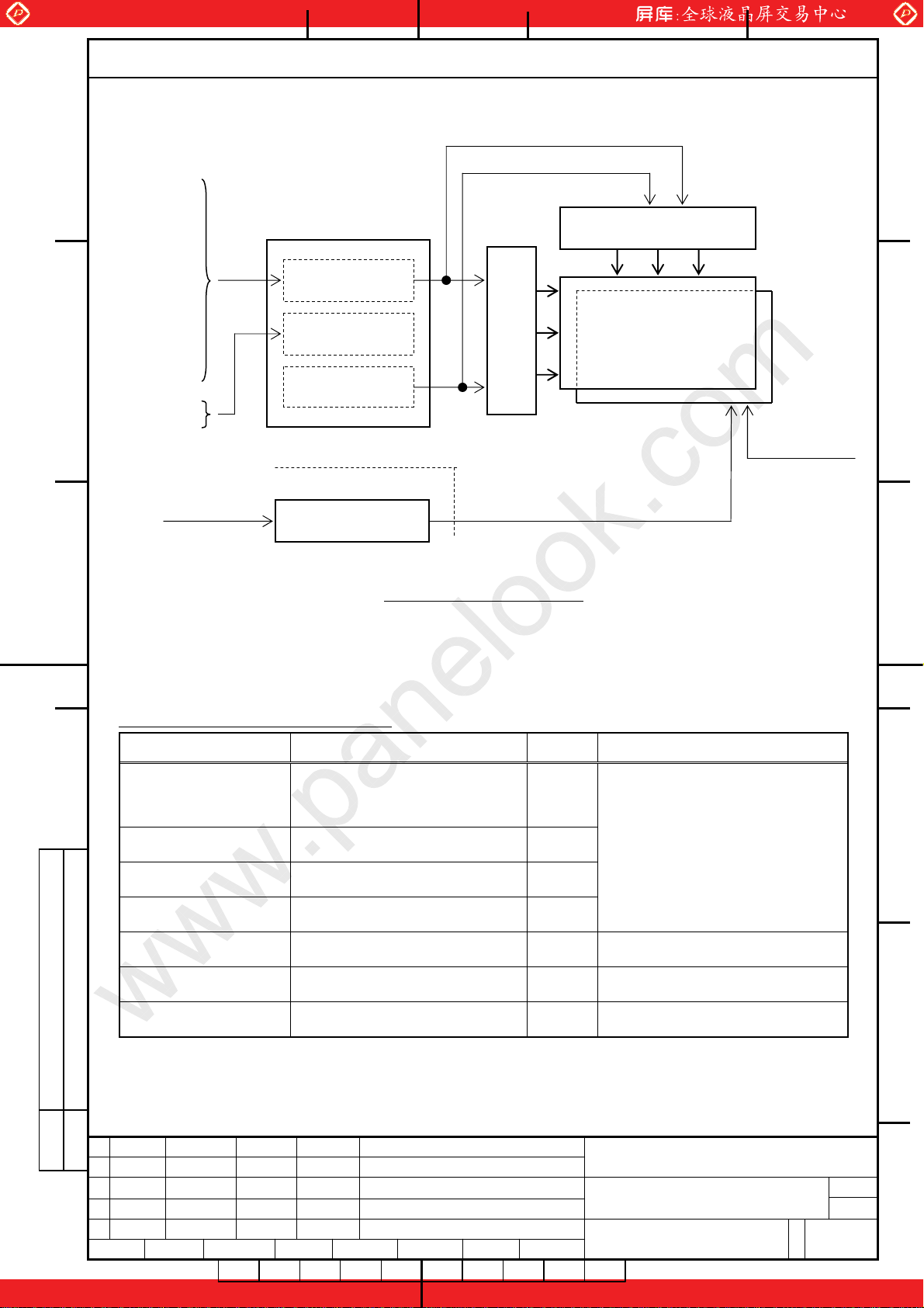
4. CONFIGURATION
www.panelook.com
ޣNA19026-C081ޤ
This specification is applied to the 17.0 in. XGA-WIDE supported TFT-LCD module.
㪘㩷
2-1. Product Name
: LCD Module
2-2. Model Name
: NA19026-C081
㪙㩷
This LCD module has a TFT active matrix type liquid crystal panel 1280×768 pixels, and
diagonal size of 43cm (17.0-inch). This module supports 1280×768 XGA-WIDE mode
(Non-interlace).
This LCD has a XGA-WIDE-capable 1ch-LVDS interface and can display 16 million colors.
By timing control signal, images are displayed on the screen at given value under specified
timing.
㪚㩷 㪚
Control signals to this LCD module are ENAB (Data enable signal), DCLK signal and RGB
data signal. Data signal is transmitted with single port. (8 bit for each R, G, B)
The power supply of this LCD module is +5V DC.
㪛㩷
This LCD module consists of a color TFT-LCD panel that mounted with TFT driver ICs, a
cold-cathode fluorescent tube back-light, a LVDS interface PCB, a structure and a bezel. And
these components are integrated in a LCD module.
Cold-cathode fluorescent tube and lamp holder are replaceable.
Fig.4-1 shows a block diagram of this LCD module.
㪛
㪜
㪛㪘㪫㪜㩷 㪛㪦㪚㪬㪤㪜㪥㪫㩷㪚㪦㪥㪫㪩㪦㪣㩷㪪㪜㪚㪫㪠㪦㪥㩷
NA19026-C081
㪜㪛㪠㪫㩷
㪛㪜㪪㪠㪞㪅㩷
㪛㪘㪫㪜㩷
㪛㪜㪪㪠㪞㪅㩷 㪛㪜㪪㪚㪩㪠㪧㪫㪠㪦㪥
㪚㪟㪜㪚㪢㩷
㪘㪧㪧㪩㪅㩷
㪚㪟㪜㪚㪢㩷
㪘㪧㪧㪩㪅
Tech Bes LCD-00223
FUJITSU DISPLAY TECHNOLOGIES
CORPORATION
㪈㩷
One step solution for LCD / PDP / OLED panel application: Datasheet, inventory and accessory!
㪚㪬㪪㪫㪅
䌓
䌈
䌅
2
/
䌅
䌔
www.panelook.com
Page 4
Global LCD Panel Exchange Center
5. MECHANICAL SPECIFICATIONS
㪘㩷
㪙㩷
Input signal
RxCLK‐
RxCLK+
Rx0‐
Rx0+
Rx1‐
Rx1+
Rx2‐
Rx2+
Rx3‐
Rx3+
Power supply
+5V DC
Interface circuit
DC/DC converter
Bias power supply
DC
(Separate)
Inverter
www.panelook.com
Gate Driver
ޣNA19026-C081ޤ
Data Driver
panel
LCD
1280×3(RGB)×768
Back light
(CCFL)
㪚㩷 㪚
Figure 4-1. Block Diagram
Table 5-1 shows the mechanical specifications of this LCD module.
㪛㩷
Table 5-1. Mechanical Specifications
Item Specifications Unit Remark
Dimensions 413.8×263.5×18.4(TYP.)
Display Resolution (1280×3) ×768 —
Display Dot Area 369.6×221.76 mm
Dot Pitch (0.09625×3) ×0.28875 mm
Aspect Ratio 1:1 —
Weight 2,000 max g
mm
Edge type backlight is used.
(I2.6 CCFL×4)
Outward Appearance is shown
at page 32 and 33.
㪛
FG-SG Short circuit —
㪛㪘㪫㪜㩷 㪛㪦㪚㪬㪤㪜㪥㪫㩷㪚㪦㪥㪫㪩㪦㪣㩷㪪㪜㪚㪫㪠㪦㪥㩷
NA19026-C081
Tech Bes LCD-00223
㪜㪛㪠㪫㩷
㪛㪜㪪㪠㪞㪅㩷
㪛㪘㪫㪜㩷
㪛㪜㪪㪠㪞㪅㩷 㪛㪜㪪㪚㪩㪠㪧㪫㪠㪦㪥
㪚㪟㪜㪚㪢㩷
㪘㪧㪧㪩㪅㩷
㪚㪟㪜㪚㪢㩷
㪘㪧㪧㪩㪅
FUJITSU DISPLAY TECHNOLOGIES
CORPORATION
㪈㩷
One step solution for LCD / PDP / OLED panel application: Datasheet, inventory and accessory!
㪜
㪚㪬㪪㪫㪅
䌓
䌈
䌅
3
/
䌅
䌔
www.panelook.com
Page 5
Global LCD Panel Exchange Center
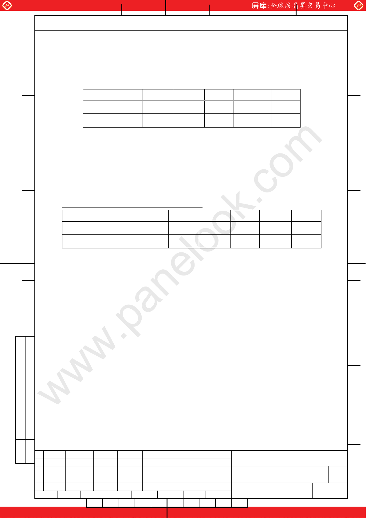
6. ABSOLUTE MAXIMUM RATINGS
−
−
7. RECOMMENDED OPERATING CONDITIONS
㪘㩷
Table 6-1 shows the absolute maximum rating of this LCD module.
Table 6-1. Absolute Maximum Ratings
Item Symbol MIN. TYP. MAX. Unit
www.panelook.com
ޣNA19026-C081ޤ
Supply Voltage V
Input Voltage V
CC
IN
0.3
0.3
— 6.0 V
— Vcc+0.3 V
㪙㩷
Table 7-1 shows the recommended operating conditions of this LCD module.
Table 7-1. Recommended Operating Conditions
Item Symbol MIN. TYP. MAX. Unit
㪚㩷 㪚
Supply Voltage V
Ripple Voltage (Vcc)
CC
V
RP
4.75 5.0 5.25 V
— — 100 mVp-p
㪛㩷
㪛㪘㪫㪜㩷 㪛㪦㪚㪬㪤㪜㪥㪫㩷㪚㪦㪥㪫㪩㪦㪣㩷㪪㪜㪚㪫㪠㪦㪥㩷
NA19026-C081
㪜㪛㪠㪫㩷
㪛㪜㪪㪠㪞㪅㩷
㪛㪘㪫㪜㩷
㪛㪜㪪㪠㪞㪅㩷 㪛㪜㪪㪚㪩㪠㪧㪫㪠㪦㪥
㪚㪟㪜㪚㪢㩷
㪘㪧㪧㪩㪅㩷
㪚㪟㪜㪚㪢㩷
㪘㪧㪧㪩㪅
Tech Bes LCD-00223
FUJITSU DISPLAY TECHNOLOGIES
CORPORATION
㪈㩷
One step solution for LCD / PDP / OLED panel application: Datasheet, inventory and accessory!
㪛
㪜
㪚㪬㪪㪫㪅
䌓
䌈
䌅
4
/
䌅
䌔
www.panelook.com
Page 6
Global LCD Panel Exchange Center
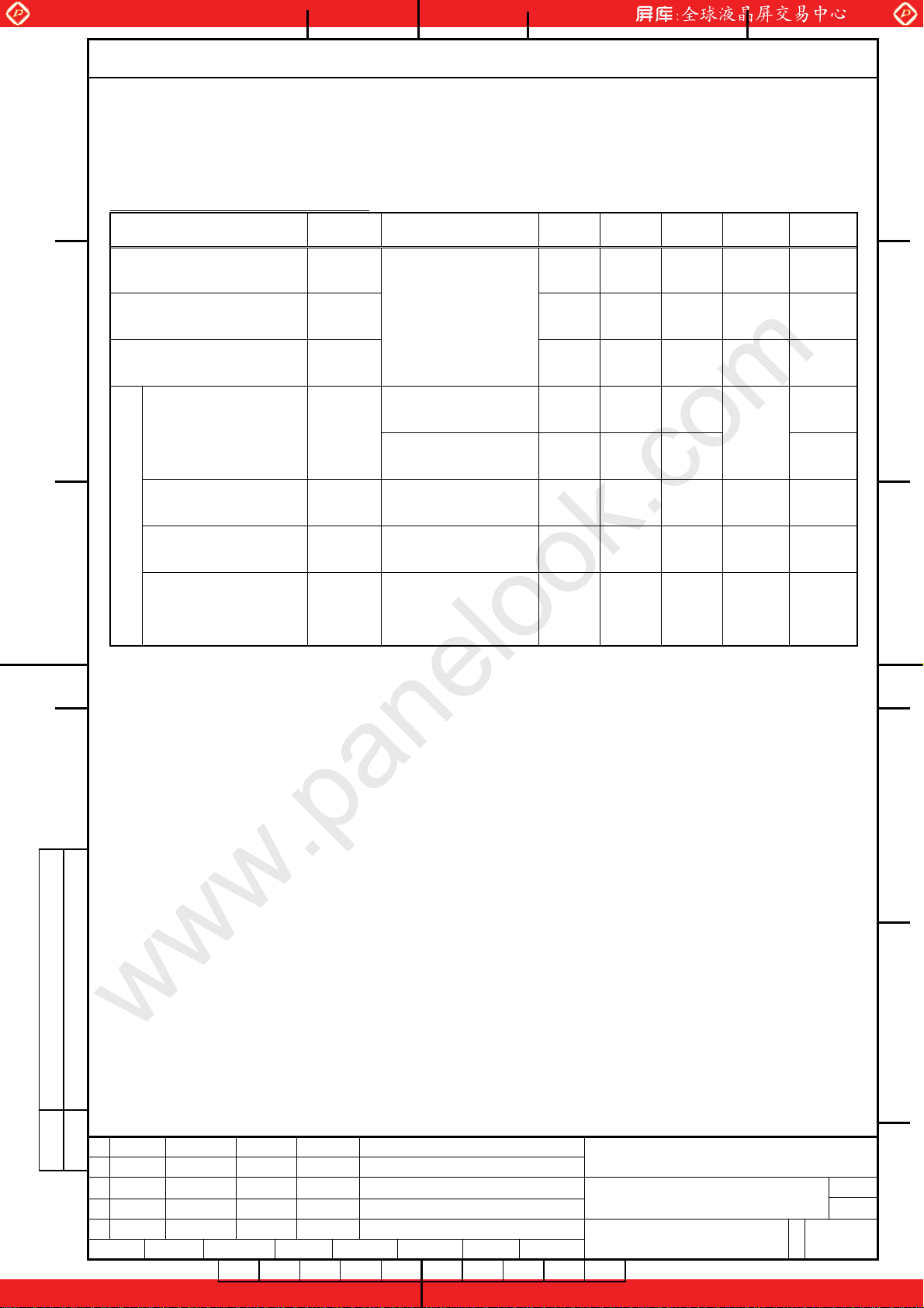
8. ELECTRICAL SPECIFICATIONS
㪘㩷
Table 8-1 shows the electrical specifications of this LCD module.
Table 8-1. Electrical Specifications
www.panelook.com
ޣNA19026-C081ޤ
Item Symbol Condition MIN. TYP. MAX. Unit
Supply Current I
CC
V
+5.0±0.25V
CC=
— 680 900 mA *1
Remark
Vss=0V
“H” Level Logic Input
Voltage
㪙㩷
“L” Level Logic Input
Voltage
CCFL Turn on
Voltage
Lighting Voltage V
V
V
V
DCLK=32.498MHz
IH
GND
IL
=50kHz,
f
L
Ta=25ºC
S
=50kHz,
f
L
Ta=0ºC
=50kHz
f
L
L
=10.5mA
I
L
0.7×
Vcc
—
—
V
CC+
0.3
0.3×
Vcc
V *2
V *2
— 1230 1600
Vrms
— — 1600
590 630 670 Vrms *4
BACK LIGHT
Lighting Frequency
㪚㩷 㪚
*3
Tube Current
f
I
L
L
=630Vrms
V
L
=50kHz
f
L
=630Vrms
V
L
40 50 60 kHz
Arms
9.5 10.5 11.0
m
*4
(*1) Typical current value is measured when gray scale (vertical 256 levels) is displayed at
Vcc=5.0V.
Maximum current value is measured when stripes with respect to each RGB dot are
displayed at Vcc=5.0V.
Without rush current.
(*2) Timing control circuit input voltage
㪛㩷
(*3) Backlight specifications are valid when using a suitable inverter such as the “FLCV-15” of
FDTC.
(*4) Tube current (I
) shows the value of the current and voltage that is consumed at one lamp.
L
(4 tubes/unit)
This LCD module has 4 lamps. Each 2 lamps are placed at upper and lower side of the
display.
2 lamps are connected in parallel. Each low voltage terminals (GND side) are bound into 1
line cable.
(See 11-1. Pin configuration for backlight)
㪛
㪜
㪛㪘㪫㪜㩷 㪛㪦㪚㪬㪤㪜㪥㪫㩷㪚㪦㪥㪫㪩㪦㪣㩷㪪㪜㪚㪫㪠㪦㪥㩷
㪜㪛㪠㪫㩷
㪛㪜㪪㪠㪞㪅㩷
㪛㪘㪫㪜㩷
㪛㪜㪪㪠㪞㪅㩷 㪛㪜㪪㪚㪩㪠㪧㪫㪠㪦㪥
㪚㪟㪜㪚㪢㩷
㪘㪧㪧㪩㪅㩷
㪚㪟㪜㪚㪢㩷
㪘㪧㪧㪩㪅
FUJITSU DISPLAY TECHNOLOGIES
NA19026-C081
Tech Bes LCD-00223
CORPORATION
㪈㩷
One step solution for LCD / PDP / OLED panel application: Datasheet, inventory and accessory!
㪚㪬㪪㪫㪅
䌓
䌈
䌅
5
/
䌅
䌔
www.panelook.com
Page 7
Global LCD Panel Exchange Center
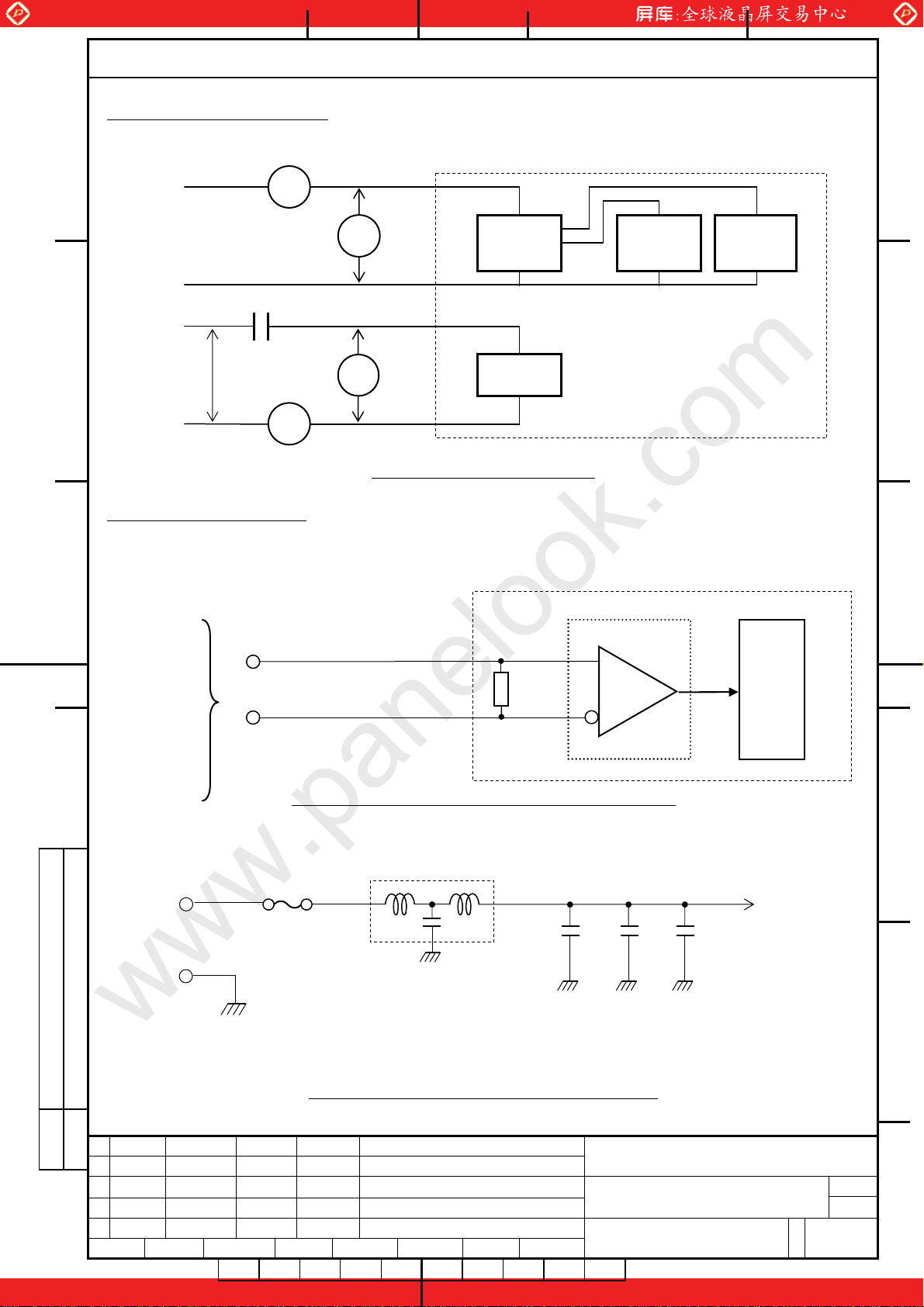
㵪
Note 1) Measurement Circuit
www.panelook.com
ޣNA19026-C081ޤ
㪘㩷
+5V
Icc
Based on Fig.8-1.
㪙㩷
Vcc
GND
AC
C
L
V
S
V
L
DC/DC
Converter
Back- light
Driver Logic㩷
GND
I
L
LCD
module
Fig.8-1. Measurement Circuit
Note 2) Equivalent Circuit
Based on Fig.8-2 (a), (b).
㪚㩷 㪚
LVDS Receiver
Internal
circuit
㪛㩷
Input signals(LVDS-1ch)
4Z%.-
4Z%.-
4Z
4Z
4Z
4Z
4Z
4Z
4Z
+
4Z
Differential Input
100㱅
Fig.8-2 (a) Equivalent Circuit of Logic Signal Input
Vcc
GND
Fuse
(2.5A)
EMI Filter
22uF
10PF
100pF
Internal
Circuit
FG
Frame ground)
(
Fuse:
EMI Filter:
KAB2402 252 NA29010(Matsuo Electric Co., Ltd.)or equivalent.
SGM20C1E332-2A(SUMITOMO Metal)or equivalent.
Fig.8-2 (b) Equivalent Circuit of Power Supply
㪛
㪜
㪛㪘㪫㪜㩷 㪛㪦㪚㪬㪤㪜㪥㪫㩷㪚㪦㪥㪫㪩㪦㪣㩷㪪㪜㪚㪫㪠㪦㪥㩷
㪜㪛㪠㪫㩷
㪛㪜㪪㪠㪞㪅㩷
㪛㪘㪫㪜㩷
㪛㪜㪪㪠㪞㪅㩷 㪛㪜㪪㪚㪩㪠㪧㪫㪠㪦㪥
㪚㪟㪜㪚㪢㩷
㪘㪧㪧㪩㪅㩷
㪚㪟㪜㪚㪢㩷
㪘㪧㪧㪩㪅
FUJITSU DISPLAY TECHNOLOGIES
NA19026-C081
Tech Bes LCD-00223
CORPORATION
㪈㩷
One step solution for LCD / PDP / OLED panel application: Datasheet, inventory and accessory!
㪚㪬㪪㪫㪅
䌓
䌈
䌅
6
/
䌅
䌔
www.panelook.com
Page 8
Global LCD Panel Exchange Center
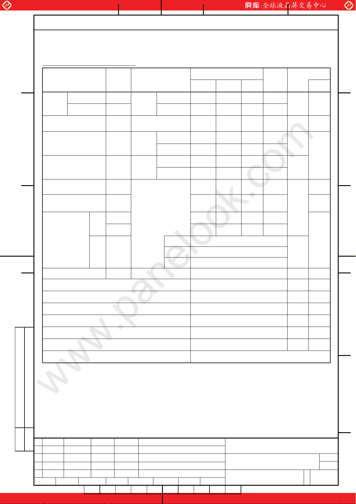
9. OPTICAL SPECIFICATIONS
㪘㩷
Table 9-1 shows the optical specifications of this LCD module.
Table 9-1. Optical Specifications
www.panelook.com
ޣNA19026-C081ޤ
Ta=25ºC
Item Symbol Condition
MIN. TYP. MAX
Visual
Angle
Horizontal
Vertical
Contrast Ratio CR
Response
㪙㩷
Time(ON)
(B→W)
Response
Time(OFF)
(W→B)
T
T
L,R
U,D
t
t
on
off
CRt10
T
L,R,U,D
T
L,R,
=0º
U,D
T
L,R,
=0º
U,D
T
=0º
U,D
T
=0º
L,R
=0º
Ta=25ºC — 15 30 ms
Ta=0ºC — 50 100 ms
Ta=25ºC — 10 25 ms
Ta=0ºC — 50 100 ms
85 — — deg
85 — — deg
350 600 — —
Brightness I 350 450 — cd/m
T
Brightness
Uniformity
Chromaticity W
㪚㩷 㪚
'I
V
I
(at maximum
X 0.283 0.313 0.343 —
brightness)
Y
=0º
L,R,U,D
=5V,
CC
=10.5mA
L
75 — — %
0.299 0.329 0.359 —
R Red 0.65, 0.34 Typ.
G Green 0.30, 0.59 Typ.
B
(x, y)
Blue 0.15, 0.14 Typ.
Unit
Note
White/
Black
2
White
*1
(1)(2)
(3)(5)
(6)
(1)(2)
(3)(5)
(1)
(4)
(5)
(1)(5)
(1)(5)
(7)
(1)
(5)
Specifications Remark
-curve
γ
γ
2.4 Typ.
LCD Panel Type TFT Color
Display Mode Normally Black VA
㪛㩷
Wide Viewing Angle Technology MVA-Premium
Optimum Viewing Angle
Display Color
− (symmetry)
16 million (each 6-bit+2-bit FRC)
Color of non-display area Black
Surface Treatment
−
(*1) Specified value is measured in 20~30 minutes after lighting on (LCD module single).
A required value may not be achieved on condition that LCD module is built in the cabinet because of
its radiation.
All items without “Brightness Uniformity” are measured at the center of display board.
(Note1) •CS-1000 (MINOLTA Co., Ltd.) , BM-5A(Topcon) or equivalent luminance colorimeter should be
used for the measurement.
Field=2º, L=500mm
•The specified value of viewing angle, contrast, brightness, brightness uniformity and
chromaticity are under the dark room condition (1lux or less).
㪛㪘㪫㪜㩷 㪛㪦㪚㪬㪤㪜㪥㪫㩷㪚㪦㪥㪫㪩㪦㪣㩷㪪㪜㪚㪫㪠㪦㪥㩷
㪜㪛㪠㪫㩷
㪛㪜㪪㪠㪞㪅㩷
㪛㪘㪫㪜㩷
㪛㪜㪪㪠㪞㪅㩷 㪛㪜㪪㪚㪩㪠㪧㪫㪠㪦㪥
㪚㪟㪜㪚㪢㩷
㪘㪧㪧㪩㪅㩷
㪚㪟㪜㪚㪢㩷
㪘㪧㪧㪩㪅
FUJITSU DISPLAY TECHNOLOGIES
NA19026-C081
Tech Bes LCD-00223
CORPORATION
㪈㩷
One step solution for LCD / PDP / OLED panel application: Datasheet, inventory and accessory!
(6)
㪛
㪜
㪚㪬㪪㪫㪅
䌓
䌈
䌅
7
/
䌅
䌔
www.panelook.com
Page 9
Global LCD Panel Exchange Center
Y
X
www.panelook.com
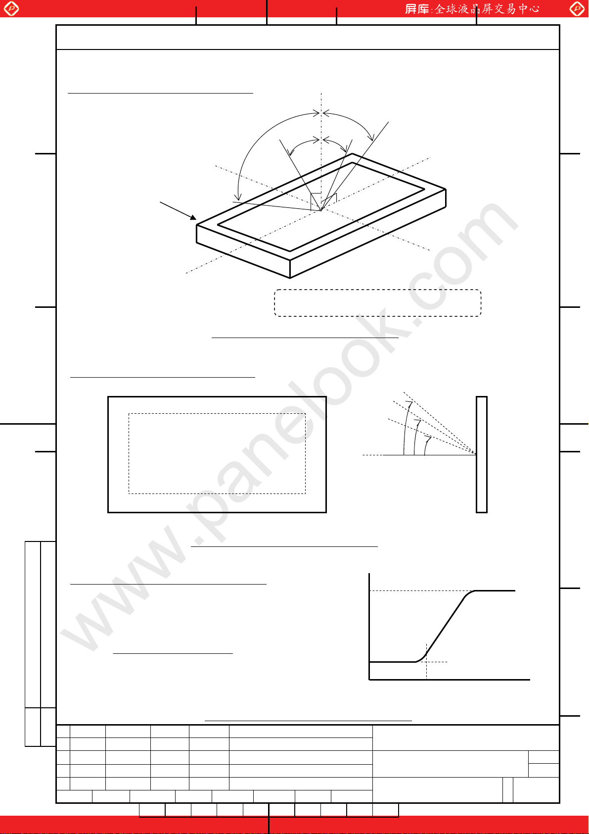
Note 1) Definition of Viewing Angle (1)
㪘㩷
Based on Fig.9-2.
㩷
Y
Top (12 o’clock Direction)
+
T
L
*0º (Front)
T
U
T
R
T
D
㩷㩷
+
Right (3 o’clock Direction)
LCD module
㪙㩷
㩷㩷㩷㩷㩷㩷㩷㩷㩷㩷X
Left (9 o’clock Direction)
㩷㩷㩷㩷㩷㩷㩷㩷㩷㩷
Bottom (6 o’clock Direction)
* o T
=0º,TD=0º,TL=0º,TR=0º
U
Fig.9-2. Definition of Viewing Angle (1)
㪚㩷 㪚
Note 2) Definition of Viewing Angle (2)
Based on Fig.9-3.
Display Surface
T
T
TYP
MAX
T
MIN
T
Display Surface
L,R,U,D
=0º
㪛㩷
Fig.9-3. Definition of Viewing Angle (2)
Note 3) Definition of Contrast Ratio (CR)
Determined by Formula (1) based on
L
W
Fig.9-4.Voltage-Brightness
Characteristics.
(Brightness at white)
L
W
= -------- (1)
(Brightness at black)
L
B
Brightness
[L]
L
0
Black
B
0
Panel Drive Voltage [V]
㪛㪘㪫㪜㩷 㪛㪦㪚㪬㪤㪜㪥㪫㩷㪚㪦㪥㪫㪩㪦㪣㩷㪪㪜㪚㪫㪠㪦㪥㩷
Fig.9-4. Voltage-Brightness Characteristics
NA19026-C081
㪜㪛㪠㪫㩷
㪛㪜㪪㪠㪞㪅㩷
㪛㪘㪫㪜㩷
㪛㪜㪪㪠㪞㪅㩷 㪛㪜㪪㪚㪩㪠㪧㪫㪠㪦㪥
㪚㪟㪜㪚㪢㩷
㪈㩷
One step solution for LCD / PDP / OLED panel application: Datasheet, inventory and accessory!
㪘㪧㪧㪩㪅㩷
㪚㪟㪜㪚㪢㩷
㪘㪧㪧㪩㪅
Tech Bes LCD-00223
FUJITSU DISPLAY TECHNOLOGIES
CORPORATION
ޣNA19026-C081ޤ
White
㪚㪬㪪㪫㪅
䌓
䌈
䌅
8
/
䌅
䌔
www.panelook.com
㪛
㪜
Page 10
Global LCD Panel Exchange Center
www.panelook.com
ޣNA19026-C081ޤ
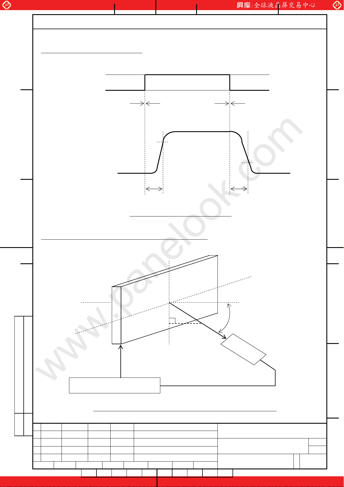
Note 4) Definition of Response Time
㪘㩷
㪙㩷
㪚㩷 㪚
Note 5) Contrast Ratio and Response Measurement System
Based on Fig.9-5.
Drive signal
of LCD panel
Non-select status
Relative
Brightness
ON
OFF
100%
0%
Select status
90%
White
Black
t
on
ON Response Time
Fig.9-5. Definition of Response Time
Non-select status
10%
Black
t
off
OFF Response Time
㪛㩷
Based on Fig.9-6.
+
Y
+
X
Z
+
Z
㪛
Brightness Meter or
T
X
Y
Luminance Colorimeter
(with luminosity
correction function)
Drive and Measurement System
㪜
Fig.9-6. Contrast Ratio and Response Time Measurement System
㪛㪘㪫㪜㩷 㪛㪦㪚㪬㪤㪜㪥㪫㩷㪚㪦㪥㪫㪩㪦㪣㩷㪪㪜㪚㪫㪠㪦㪥㩷
㪜㪛㪠㪫㩷
㪛㪜㪪㪠㪞㪅㩷
㪛㪘㪫㪜㩷
㪛㪜㪪㪠㪞㪅㩷 㪛㪜㪪㪚㪩㪠㪧㪫㪠㪦㪥
㪚㪟㪜㪚㪢㩷
㪘㪧㪧㪩㪅㩷
㪚㪟㪜㪚㪢㩷
㪘㪧㪧㪩㪅
FUJITSU DISPLAY TECHNOLOGIES
NA19026-C081
Tech Bes LCD-00223
CORPORATION
㪈㩷
One step solution for LCD / PDP / OLED panel application: Datasheet, inventory and accessory!
㪚㪬㪪㪫㪅
䌓
䌈
䌅
9
/
䌅
䌔
www.panelook.com
Page 11

Global LCD Panel Exchange Center
Note 6) Definition of Optimum Viewing Angle
㪘㩷
Based on Fig.9-7.
www.panelook.com
ޣNA19026-C081ޤ
㩷 MAX
Contrast
Ratio
㪙㩷
10
(-)
6 o’clock m Viewing Angle o 12 o’clock
(+) 0
Fig.9-7. Definition of Viewing Angle
Note 7) Definition of Brightness Uniformity
㪚㩷 㪚
Brightness uniformity is defined by the following formula.
Brightness (I1~I9) art measured at the following 9 points ( 1 ~ 9 ) on the display
area shown in Fig.9-8.
|Min. In|
Brightness Uniformity ('L) = × 100 (%), n=1 to 9
|Max. In|
192 640 1088
㪛㩷
1 4 7
115
2 5 8
384
3 6 9
653
Note) Each measurement point ( 1 ~ 9 ) defines the center spot of Brightness Meter view.
The tolerance of measurement position is ±3mm.
Fig.9-8. Measurement Points
㪛㪘㪫㪜㩷 㪛㪦㪚㪬㪤㪜㪥㪫㩷㪚㪦㪥㪫㪩㪦㪣㩷㪪㪜㪚㪫㪠㪦㪥㩷
NA19026-C081
Tech Bes LCD-00223
㪜㪛㪠㪫㩷
㪛㪜㪪㪠㪞㪅㩷
㪛㪘㪫㪜㩷
㪛㪜㪪㪠㪞㪅㩷 㪛㪜㪪㪚㪩㪠㪧㪫㪠㪦㪥
㪚㪟㪜㪚㪢㩷
㪘㪧㪧㪩㪅㩷
㪚㪟㪜㪚㪢㩷
㪘㪧㪧㪩㪅
FUJITSU DISPLAY TECHNOLOGIES
CORPORATION
㪈㩷
One step solution for LCD / PDP / OLED panel application: Datasheet, inventory and accessory!
㪛
㪜
㪚㪬㪪㪫㪅
䌓
䌈
䌅
10
/
䌅
䌔
www.panelook.com
Page 12

Global LCD Panel Exchange Center
10. INTERFACE SPECIFICATIONS
y
y
10-1-1. Signal descriptions
www.panelook.com
ޣNA19026-C081ޤ
㪘㩷
Table 10-1 shows the description and configuration of Interface signals (CN1).
Table 10-1-1. Interface signals (CN1)
Pin
№
1 VDD
2 VDD
3 GND
4 GND
㪙㩷
5 RX0 6 RX0+
7 GND
8 RX1 9 RX1+
10 GND
11 RX212 RX2+
13 GND
14 RXCLK-
15 RXCLK+
16 GND
㪚㩷 㪚
17 RX318 RX3+
19 GND
20
Symbol I/O Function
−
−
−
−
−
−
−
−
−
Data Mapping
Select Input
+5V Power supl
+5V Power supl
Ground
Ground
LVDS Receiver Signal(-)
I
LVDS Receiver Signal(+)
I
Ground
LVDS Receiver Signal(-)
I
LVDS Receiver Signal(+)
I
Ground
LVDS Receiver Signal(-)
I
LVDS Receiver Signal(+)
I
Ground
LVDS Receiver Clock Signal(-)
I
LVDS Receiver Clock Signal(+)
I
Ground
LVDS Receiver Signal(-)
I
LVDS Receiver Signal(+)
I
Ground
Low : table 10-1-2
I
Open or Hi : table 10-1-3
Upper side
㪛㩷
㩷 Interface connector
LCD Module
Rear side
20
Connector :D14H-20P-1.25H(HIROSE)
User’s connector :DF14-20S-1.25 (HIROSE)
1
㩷㩷㩷㩷㩷㩷㩷㩷㩷㩷㩷㩷㩷㩷㩷㩷㩷㩷㩷㩷㩷㩷㩷㩷㩷㩷㩷㩷㩷㩷㩷㩷Note)When using a interface connector other
Lower side
than the recommended one, a defect in the
initial stage or a problem concerning long
term reliabiliting may occur.
DATE DOCUMENT CONTROL SECTION
NA19026-C081
Tech Bes LCD-00223
EDIT
DESIG.
DATE
DESIG.
CHECK
CHECK
APPR.
DESCRIPTION
APPR.
FUJITSU DISPLAY TECHNOLOGIES
CORPORATION
㪈㩷
One step solution for LCD / PDP / OLED panel application: Datasheet, inventory and accessory!
㪛
㪜
CUST.
SHEET
11
/
www.panelook.com
Page 13

Global LCD Panel Exchange Center
㪂
㪂
10-1-2. LVDS Data Mapping 1
Table 10-1-2 shows the LVDS data mapping 1.(DataMappingSelectInput = Low)
www.panelook.com
ޣNA19026-C081ޤ
㪘㩷
Table 10-1-2. LVDS Data Mapping 1
㪫㫉㪸㫅㫊㫄㫀㫋㫋㪼㫉
㪛㪪㪐㪇㪚㪝㪊㪏㪌㪀
㩿
㪪㫐㫄㪹㫆㫃
㪠㫅㫋㪼㫉㪽㪸㪺㪼㩷㪺㫆㫅㫅㪼㪺㫋㫆㫉
㪧㫀㫅 㪠㪥㪧㪬㪫 㪪㫐㫊㫋㪼㫄㩷㫊㫀㪻㪼 㪧㫀㫅 㪣㪚㪛㩷㫄㫆㪻㫌㫃㪼 㪧㫀㫅 㪦㪬㪫㪧㪬㪫
㪌㪈 㪫㫏㪠㪥㪇 䌒䋰 㪉㪎 㪩㫏㪦㪬㪫㪇 䌉䌒䋰
㪌㪉 㪫㫏㪠㪥㪈 䌒䋱 㪉㪐 㪩㫏㪦㪬㪫㪈 䌉䌒䋱
㪌㪋 㪫㫏㪠㪥㪉 䌒䋲 㪊㪇 㪩㫏㪦㪬㪫㪉 䌉䌒䋲
㪌㪌 㪫㫏㪠㪥㪊 䌒䋳 㪊㪉 㪩㫏㪦㪬㪫㪊 䌉䌒䋳
㪙㩷
㪌㪍 㪫㫏㪠㪥㪋 䌒䋴 㪊㪊 㪩㫏㪦㪬㪫㪋 䌉䌒䋴
㪉㪫㫏㪠㪥㪌 䌒䋷
㪊㪫㫏㪠㪥㪍 䌒䋵 㪊㪌㪩㫏㪦㪬㪫㪍 䌉䌒䋵
㪋㪫㫏㪠㪥㪎 䌇䋰 㪊㪎㪩㫏㪦㪬㪫㪎 䌉䌇䋰
㪍㪫㫏㪠㪥㪏 䌇䋱 㪊㪏㪩㫏㪦㪬㪫㪏 䌉䌇䋱
㪎㪫㫏㪠㪥㪐 䌇䋲 㪊㪐㪩㫏㪦㪬㪫㪐 䌉䌇䋲
㪏 㪫㫏㪠㪥㪈㪇 䌇䋶 㪋㪈 㪩㫏㪦㪬㪫㪈㪇 䌉䌇䋶
㪈㪇 㪫㫏㪠㪥㪈㪈 䌇䋷 㪋㪉 㪩㫏㪦㪬㪫㪈㪈 䌉䌇䋷
㪈㪈 㪫㫏㪠㪥㪈㪉 䌇䋳 㪋㪊 㪩㫏㪦㪬㪫㪈㪉 䌉䌇䋳
㪈㪉 㪫㫏㪠㪥㪈㪊 䌇䋴 㪋㪌 㪩㫏㪦㪬㪫㪈㪊 䌉䌇䋴
㪈㪋 㪫㫏㪠㪥㪈㪋 䌇䋵 㪋㪍 㪩㫏㪦㪬㪫㪈㪋 䌉䌇䋵
㪚㩷 㪚
㪛㩷
㪈㪌 㪫㫏㪠㪥㪈㪌 䌂䋰 㪋㪎 㪩㫏㪦㪬㪫㪈㪌 䌉䌂䋰
㪈㪍 㪫㫏㪠㪥㪈㪍 䌂䋶 㪋㪐 㪩㫏㪦㪬㪫㪈㪍 䌉䌂䋶
㪈㪏 㪫㫏㪠㪥㪈㪎 䌂䋷 㪌㪇 㪩㫏㪦㪬㪫㪈㪎 䌉䌂䋷
㪈㪐 㪫㫏㪠㪥㪈㪏 䌂䋱
㪉㪇 㪫㫏㪠㪥㪈㪐 䌂䋲 㪌㪊 㪩㫏㪦㪬㪫㪈㪐 䌉䌂䋲
㪉㪉 㪫㫏㪠㪥㪉㪇 䌂䋳 㪌㪋 㪩㫏㪦㪬㪫㪉㪇 䌉䌂䋳
㪉㪊 㪫㫏㪠㪥㪉㪈 䌂䋴 㪌㪌 㪩㫏㪦㪬㪫㪉㪈 䌉䌂䋴
㪉㪋 㪫㫏㪠㪥㪉㪉 䌂䋵 㪈 㪩㫏㪦㪬㪫㪉㪉 䌉䌂䋵
㪉㪌 㪫㫏㪠㪥㪉㪊 㪩㪜㪪㪜㪩㪭㪜㪛
㪉㪎 㪫㫏㪠㪥㪉㪋 㪩㪜㪪㪜㪩㪭㪜㪛 㪊 㪩㫏㪦㪬㪫㪉㪋 㪥㫆㫋㩷㫌㫊㪼
㪉㪏 㪫㫏㪠㪥㪉㪌 㪩㪜㪪㪜㪩㪭㪜㪛 㪌 㪩㫏㪦㪬㪫㪉㪌 㪥㫆㫋㩷㫌㫊㪼
㪊㪇 㪫㫏㪠㪥㪉㪍 㪜㪥㪘㪙 㪍 㪩㫏㪦㪬㪫㪉㪍 䌅䌎䌁䌂
㪌㪇 㪫㫏㪠㪥㪉㪎 䌒䋶
㪊㪈 㪫㫏㪚㪣㪢㪠㪥
㪛㪚㪣㪢
㪫㫏㪦㪬㪫㪇㪄
㪫㫏㪦㪬㪫㪇㪂
㪫㫏㪦㪬㪫㪊㪄
㪫㫏㪦㪬㪫㪊㪂
㪫㫏㪦㪬㪫㪇㪄
㪫㫏㪦㪬㪫㪇㪂
㪫㫏㪦㪬㪫㪈㪄
㪫㫏㪦㪬㪫㪈㪂
㪫㫏㪦㪬㪫㪊㪄
㪫㫏㪦㪬㪫㪊㪂
㪫㫏㪦㪬㪫㪈㪄
㪫㫏㪦㪬㪫㪈㪂
㪫㫏㪦㪬㪫㪊㪄
㪫㫏㪦㪬㪫㪊㪂
㪫㫏㪦㪬㪫㪈㪄
㪫㫏㪦㪬㪫㪈㪂
㪫㫏㪦㪬㪫㪉㪄
㪫㫏㪦㪬㪫㪉㪂
㪫㫏㪦㪬㪫㪊㪄
㪫㫏㪦㪬㪫㪊㪂
㪫㫏㪦㪬㪫㪉㪄
㪫㫏㪦㪬㪫㪉㪂
㪫㫏㪦㪬㪫㪊㪄
㪫㫏㪦㪬㪫㪊㪂
㪫㫏㪚㪣㪢㪦㪬㪫㪄
㪫㫏㪚㪣㪢㪦㪬㪫㪂
㪈㪎
㪈㪏
㪈㪎
㪈㪏
㪈㪎
㪈㪏
㪈㪈
㪈㪉
㪈㪎
㪈㪏
㪈㪈
㪈㪉
㪈㪎
㪈㪏
㪈㪋
㪈㪌
㪩㪼㪺㪼㫀㫍㪼㫉
㪛㪪㪐㪇㪚㪝㪊㪏㪍㪀
㩿
㪣㪚㪛
㪚㫆㫅㫋㫉㫆㫃
㫀㫅㫇㫌㫋
㪌
㪍
㪌
㪍
㪏
㪐
㪩㪯㪇㪄
㪩㪯㪇㪂
㪩㪯㪊㪄
㪩㪯㪊
㪩㪯㪇㪄
㪩㪯㪇㪂
㪩㪯㪈㪄
㪩㪯㪈㪂
㪊㪋 㪩㫏㪦㪬㪫㪌 䌉䌒䋷
㪩㪯㪊㪄
㪩㪯㪊㪂
㪏
㪐
㪩㪯㪈㪄
㪩㪯㪈㪂
㪩㪯㪊㪄
㪩㪯㪊㪂
㪏
㪐
㪩㪯㪈㪄
㪩㪯㪈㪂
㪌㪈 㪩㫏㪦㪬㪫㪈㪏 䌉䌂䋱
㪩㪯㪉㪄
㪩㪯㪉㪂
㪩㪯㪊㪄
㪩㪯㪊㪂
㪉 㪩㫏㪦㪬㪫㪉㪊 㪥㫆㫋㩷㫌㫊㪼
㪩㪯㪉㪄
㪩㪯㪉㪂
㪩㪯㪊㪄
㪩㪯㪊
㪩㪯㪚㪣㪢㪄
㪩㪯㪚㪣㪢㪂
㪎㪩㫏㪦㪬㪫㪉㪎 䌉䌒䋶
㪉㪍
㪩㫏㪚㪣㪢㪦㪬㪫 䌄䌃䌌䌋
㪛
DATE DOCUMENT CONTROL SECTION
One step solution for LCD / PDP / OLED panel application: Datasheet, inventory and accessory!
EDIT
DESIG.
DATE
DESIG.
㪈㩷
CHECK
CHECK
APPR.
DESCRIPTION
APPR.
FUJITSU DISPLAY TECHNOLOGIES
NA19026-C081
Tech Bes LCD-00223
CORPORATION
㪜
CUST.
SHEET
12
/
www.panelook.com
Page 14

Global LCD Panel Exchange Center
10-1-3. LVDS Data Mapping 2
Table 10-1-3 shows the LVDS data mapping 2.(DataMappingSelectInput = Open or Hi)
www.panelook.com
ޣNA19026-C081ޤ
㪘㩷
Table 10-1-3. LVDS Data Mapping 2
㪫㫉㪸㫅㫊㫄㫀㫋㫋㪼㫉
㩿
㪛㪪㪐㪇㪚㪝㪊㪏㪌㪀
㪪㫐㫄㪹㫆㫃
㪠㫅㫋㪼㫉㪽㪸㪺㪼㩷㪺㫆㫅㫅㪼㪺㫋㫆㫉
㪧㫀㫅 㪠㪥㪧㪬㪫 㪪㫐㫊㫋㪼㫄㩷㫊㫀㪻㪼 㪧㫀㫅 㪣㪚㪛㩷㫄㫆㪻㫌㫃㪼 㪧㫀㫅 㪦㪬㪫㪧㪬㪫
㪌㪈 㪫㫏㪠㪥㪇 䌒䋲 㪉㪎 㪩㫏㪦㪬㪫㪇 䌉䌒䋲
㪌㪉 㪫㫏㪠㪥㪈 䌒䋳 㪉㪐 㪩㫏㪦㪬㪫㪈 䌉䌒䋳
㪌㪋 㪫㫏㪠㪥㪉 䌒䋴 㪊㪇 㪩㫏㪦㪬㪫㪉 䌉䌒䋴
㪌㪌 㪫㫏㪠㪥㪊 䌒䋵 㪊㪉 㪩㫏㪦㪬㪫㪊 䌉䌒䋵
㪙㩷
㪌㪍 㪫㫏㪠㪥㪋 䌒䋶 㪊㪊 㪩㫏㪦㪬㪫㪋 䌉䌒䋶
㪉㪫㫏㪠㪥㪌 䌒䋱
㪊㪫㫏㪠㪥㪍 䌒䋷 㪊㪌㪩㫏㪦㪬㪫㪍 䌉䌒䋷
㪋㪫㫏㪠㪥㪎 䌇䋲 㪊㪎㪩㫏㪦㪬㪫㪎 䌉䌇䋲
㪍㪫㫏㪠㪥㪏 䌇䋳 㪊㪏㪩㫏㪦㪬㪫㪏 䌉䌇䋳
㪎㪫㫏㪠㪥㪐 䌇䋴 㪊㪐㪩㫏㪦㪬㪫㪐 䌉䌇䋴
㪏 㪫㫏㪠㪥㪈㪇 䌇䋰 㪋㪈 㪩㫏㪦㪬㪫㪈㪇 䌉䌇䋰
㪈㪇 㪫㫏㪠㪥㪈㪈 䌇䋱 㪋㪉 㪩㫏㪦㪬㪫㪈㪈 䌉䌇䋱
㪈㪈 㪫㫏㪠㪥㪈㪉 䌇䋵 㪋㪊 㪩㫏㪦㪬㪫㪈㪉 䌉䌇䋵
㪈㪉 㪫㫏㪠㪥㪈㪊 䌇䋶 㪋㪌 㪩㫏㪦㪬㪫㪈㪊 䌉䌇䋶
㪈㪋 㪫㫏㪠㪥㪈㪋 䌇䋷 㪋㪍 㪩㫏㪦㪬㪫㪈㪋 䌉䌇䋷
㪚㩷 㪚
㪛㩷
㪈㪌 㪫㫏㪠㪥㪈㪌 䌂䋲 㪋㪎 㪩㫏㪦㪬㪫㪈㪌 䌉䌂䋲
㪈㪍 㪫㫏㪠㪥㪈㪍 䌂䋰 㪋㪐 㪩㫏㪦㪬㪫㪈㪍 䌉䌂䋰
㪈㪏 㪫㫏㪠㪥㪈㪎 䌂䋱 㪌㪇 㪩㫏㪦㪬㪫㪈㪎 䌉䌂䋱
㪈㪐 㪫㫏㪠㪥㪈㪏 䌂䋳
㪉㪇 㪫㫏㪠㪥㪈㪐 䌂䋴 㪌㪊 㪩㫏㪦㪬㪫㪈㪐 䌉䌂䋴
㪉㪉 㪫㫏㪠㪥㪉㪇 䌂䋵 㪌㪋 㪩㫏㪦㪬㪫㪉㪇 䌉䌂䋵
㪉㪊 㪫㫏㪠㪥㪉㪈 䌂䋶 㪌㪌 㪩㫏㪦㪬㪫㪉㪈 䌉䌂䋶
㪉㪋 㪫㫏㪠㪥㪉㪉 䌂䋷 㪈 㪩㫏㪦㪬㪫㪉㪉 䌉䌂䋷
㪉㪌 㪫㫏㪠㪥㪉㪊 㪩㪜㪪㪜㪩㪭㪜㪛
㪉㪎 㪫㫏㪠㪥㪉㪋 㪩㪜㪪㪜㪩㪭㪜㪛 㪊 㪩㫏㪦㪬㪫㪉㪋 㪥㫆㫋㩷㫌㫊㪼
㪉㪏 㪫㫏㪠㪥㪉㪌 㪩㪜㪪㪜㪩㪭㪜㪛 㪌 㪩㫏㪦㪬㪫㪉㪌 㪥㫆㫋㩷㫌㫊㪼
㪊㪇 㪫㫏㪠㪥㪉㪍 㪜㪥㪘㪙 㪍 㪩㫏㪦㪬㪫㪉㪍 䌅䌎䌁䌂
㪌㪇 㪫㫏㪠㪥㪉㪎 䌒䋰
㪊㪈 㪫㫏㪚㪣㪢㪠㪥
㪛㪚㪣㪢
㪫㫏㪦㪬㪫㪇㪄
㪫㫏㪦㪬㪫㪇㪂
㪫㫏㪦㪬㪫㪊㪄
㪫㫏㪦㪬㪫㪊㪂
㪫㫏㪦㪬㪫㪇㪄
㪫㫏㪦㪬㪫㪇㪂
㪫㫏㪦㪬㪫㪈㪄
㪫㫏㪦㪬㪫㪈㪂
㪫㫏㪦㪬㪫㪊㪄
㪫㫏㪦㪬㪫㪊㪂
㪫㫏㪦㪬㪫㪈㪄
㪫㫏㪦㪬㪫㪈㪂
㪫㫏㪦㪬㪫㪊㪄
㪫㫏㪦㪬㪫㪊㪂
㪫㫏㪦㪬㪫㪈㪄
㪫㫏㪦㪬㪫㪈㪂
㪫㫏㪦㪬㪫㪉㪄
㪫㫏㪦㪬㪫㪉㪂
㪫㫏㪦㪬㪫㪊㪄
㪫㫏㪦㪬㪫㪊㪂
㪫㫏㪦㪬㪫㪉㪄
㪫㫏㪦㪬㪫㪉㪂
㪫㫏㪦㪬㪫㪊㪄
㪫㫏㪦㪬㪫㪊㪂
㪫㫏㪚㪣㪢㪦㪬㪫㪄
㪫㫏㪚㪣㪢㪦㪬㪫㪂
㪈㪎
㪈㪏
㪈㪎
㪈㪏
㪈㪎
㪈㪏
㪈㪈
㪈㪉
㪈㪎
㪈㪏
㪈㪈
㪈㪉
㪈㪎
㪈㪏
㪈㪋
㪈㪌
㪩㪼㪺㪼㫀㫍㪼㫉
㩿
㪛㪪㪐㪇㪚㪝㪊㪏㪍㪀
㪣㪚㪛
㪚㫆㫅㫋㫉㫆㫃
㫀㫅㫇㫌㫋
㪌
㪍
㪌
㪍
㪏
㪐
㪩㪯㪇㪄
㪩㪯㪇㪂
㪩㪯㪊㪄
㪩㪯㪊㪂
㪩㪯㪇㪄
㪩㪯㪇㪂
㪩㪯㪈㪄
㪩㪯㪈㪂
㪊㪋 㪩㫏㪦㪬㪫㪌 䌉䌒䋱
㪩㪯㪊㪄
㪩㪯㪊㪂
㪏
㪐
㪩㪯㪈㪄
㪩㪯㪈㪂
㪩㪯㪊㪄
㪩㪯㪊㪂
㪏
㪐
㪩㪯㪈㪄
㪩㪯㪈㪂
㪌㪈 㪩㫏㪦㪬㪫㪈㪏 䌉䌂䋳
㪩㪯㪉㪄
㪩㪯㪉㪂
㪩㪯㪊㪄
㪩㪯㪊㪂
㪉 㪩㫏㪦㪬㪫㪉㪊 㪥㫆㫋㩷㫌㫊㪼
㪩㪯㪉㪄
㪩㪯㪉㪂
㪩㪯㪊㪄
㪩㪯㪊㪂
㪩㪯㪚㪣㪢㪄
㪩㪯㪚㪣㪢㪂
㪎㪩㫏㪦㪬㪫㪉㪎 䌉䌒䋰
㪩㫏㪚㪣㪢㪦㪬㪫 䌄䌃䌌䌋
㪉㪍
㪛
DATE DOCUMENT CONTROL SECTION
EDIT
DESIG.
DATE
DESIG.
㪈㩷
CHECK
CHECK
APPR.
DESCRIPTION
APPR.
FUJITSU DISPLAY TECHNOLOGIES
NA19026-C081
Tech Bes LCD-00223
CORPORATION
One step solution for LCD / PDP / OLED panel application: Datasheet, inventory and accessory!
㪜
CUST.
SHEET
13
/
www.panelook.com
Page 15

Global LCD Panel Exchange Center
10-2. Color Data Assignment
Table 10-2 shows the color data assignment.
㪘㩷
Table 10-2. Color Data Assignment
www.panelook.com
ޣNA19026-C081ޤ
0
0
0
0
1
1
1
1
0
0
0
:
:
:
1
1
1
0
0
0
:
:
:
0
0
0
0
0
0
:
:
:
0
0
0
Input data
0
0
0
0
0
0
0
0
1
1
1
1
1
1
1
1
0
0
0
0
1
0
:
:
:
:
:
:
0
1
1
1
1
1
0
0
0
0
0
0
:
:
:
:
:
:
0
0
0
0
0
0
0
0
0
0
0
0
:
:
:
:
:
:
0
0
0
0
0
0
Colorand
Brightness
Black
Blue
Green
Cyan
Red
㪙㩷
Yellow
Magenta
Basic Color
White
Black
×
Darker
×
Red
Ø
Brighter
Ø
Red
㪚㩷 㪚
Black
×
Darker
×
Green
Ø
Brighter
Ø
Green
㪛㩷
Black
×
Darker
×
Blue
Ø
Brighter
Ø
Blue
R7R6R5R4R3R2R1R0 G7G6G5G4G3G2G1G0 B7B6B5B4B3B2B1B0
0
0
0
0
0
0
0
0
0
0
0
0
0
0
0
0
1
1
1
1
1
1
1
1
1
1
1
1
1
1
1
1
0
0
0
0
253
254
255
253
254
255
253
254
255
0
1
2
:
:
0
1
2
:
:
0
1
2
:
:
0
0
0
0
:
:
:
:
:
:
1
1
1
1
1
1
0
0
0
0
0
0
:
:
:
:
:
:
0
0
0
0
0
0
0
0
0
0
0
0
:
:
:
:
:
:
0
0
0
0
0
0
0
0
0
0
:
:
:
:
:
:
1
1
1
1
1
1
0
0
0
0
0
0
:
:
:
:
:
:
0
0
0
0
0
0
0
0
0
0
0
0
:
:
:
:
:
:
0
0
0
0
0
0
(0:
0
0
0
0
1
0
1
0
0
1
0
1
1
1
1
1
0
0
0
1
0
0
:
:
:
:
:
:
0
1
0
0
0
1
0
0
0
0
0
0
:
:
:
:
:
:
1
0
1
0
1
0
0
0
0
0
0
0
:
:
:
:
:
:
0
0
0
0
0
0
0
0
1
1
0
0
1
1
0
0
0
:
:
:
0
0
0
0
0
0
:
:
:
1
1
1
0
0
0
:
:
:
0
0
0
Low level
0
0
0
0
1
1
1
1
0
0
0
0
1
1
1
1
0
0
0
0
0
0
:
:
:
:
:
:
0
0
0
0
0
0
0
0
0
0
0
0
:
:
:
:
:
:
1
1
1
1
1
1
0
0
0
0
0
0
:
:
:
:
:
:
0
0
0
0
0
0
0
0
1
1
0
0
1
1
0
0
0
:
:
:
0
0
0
0
0
0
:
:
:
1
1
1
0
0
0
:
:
:
0
0
0
,1:
0
0
1
1
0
0
1
1
0
0
0
:
:
:
0
0
0
0
0
0
:
:
:
1
1
1
0
0
0
:
:
:
0
0
0
High level
0
0
0
0
1
1
1
1
0
0
0
0
1
1
1
1
0
0
0
0
0
0
:
:
:
:
:
:
0
0
0
0
0
0
0
0
1
0
0
1
:
:
:
:
:
:
1
0
0
1
1
1
0
0
0
0
0
0
:
:
:
:
:
:
0
0
0
0
0
0
0
1
0
1
0
1
0
1
0
0
0
:
:
:
0
0
0
0
0
0
:
:
:
0
0
0
0
0
0
:
:
:
1
1
1
)
0
1
0
1
0
1
0
1
0
0
0
:
:
:
0
0
0
0
0
0
:
:
:
0
0
0
0
0
0
:
:
:
1
1
1
0
1
0
1
0
1
0
1
0
0
0
:
:
:
0
0
0
0
0
0
:
:
:
0
0
0
0
0
0
:
:
:
1
1
1
0
1
0
1
0
1
0
1
0
0
0
:
:
:
0
0
0
0
0
0
:
:
:
0
0
0
0
0
0
:
:
:
1
1
1
0
0
0
0
1
1
1
1
0
0
0
0
1
1
1
1
0
0
0
0
1
1
1
1
0
0
0
0
1
1
1
1
0
0
0
0
0
0
0
0
0
0
0
0
:
:
:
:
:
:
:
:
:
:
:
:
0
0
0
0
0
0
0
0
0
0
0
0
0
0
0
0
0
0
0
0
0
0
0
0
:
:
:
:
:
:
:
:
:
:
:
:
0
0
0
0
0
0
0
0
0
0
0
0
0
0
0
0
1
0
0
0
0
1
0
0
:
:
:
:
:
:
:
:
:
:
:
:
1
0
1
1
0
1
1
1
1
1
1
1
㪛
Note.1) Definition of gray scale : Color (n) ---”n” indicates gray scale level.
The gray scale is brighter as the number is larger.
Note.2) Data; 1: High, 0: Low
Note.3) By inputting 8-bit data signal for each red, green and blue, this module can display 256
gray scale independently for each color.
Therefore, the module is able to display 16 million colors. Color data are 24 lines.
DATE DOCUMENT CONTROL SECTION
NA19026-C081
Tech Bes LCD-00223
EDIT
DESIG.
DATE
DESIG.
CHECK
CHECK
APPR.
DESCRIPTION
APPR.
FUJITSU DISPLAY TECHNOLOGIES
CORPORATION
㪈㩷
One step solution for LCD / PDP / OLED panel application: Datasheet, inventory and accessory!
㪜
CUST.
SHEET
14
/
www.panelook.com
Page 16

Global LCD Panel Exchange Center
10-3. Input Signal Timing
Table 10-3 and Fig.10-3 shows the input signal timing.
www.panelook.com
ޣNA19026-C081ޤ
Table 10-3. Timing Characteristics
㪘㩷
(T=0~50ºC, Vcc=5±0.25V)
Item Symbol Min. Typ. Max. Unit Remark
DCLK signal Period Tc 12.195 15.382 20.000 ns
(Clock)
Frequency fc 50.00 65.01 82.00 MHz fc=1/Tc
Duty Tch/Tc 45 50 55 % *1
High time TclkH 5.0 — — ns
Low time TclkL 5.0 — — ns
Rise time Tclkr — — 5.0 ns
Fall time Tclkf — — 5.0 ns
㪙㩷
DCLK-Data Setup time Tset 4 — — ns
Timing Hold time Thold 4 — — ns
Horizontal Period Th 1310 1344 1688 DCLK
Frequency fh 35.0 48.3 75.0 kHz
Display period Thd 1280 1280 1280 DCLK *2,3
Vertical Period Tv 776 806 806 Th 16.67ms
Frequency 1/Tv 50 60 75 Hz WXGA mode
Display period Tvd 768 768 768 Th *2,3
Data-ENAB timing
Data-ENAB timing Tdn 0 0 0 DCLK *4
*1) DCLK signal input must be valid while power supply is applied.
㪚㩷 㪚
*2) Display position is specified by the ENAB signal only.
Horizontal display position is specified by the rise of ENAB signal. The data which is
・
latched by the falling edge of 1st DCLK right after the rise of ENAB, is displayed on the
left edge of the screen.
Vertical display position is specified by the rise of ENAB after a “Low” level period
・
equivalent to eight times of horizontal period. The 1st data corresponding to one horizontal
line after the rise of ENAB is displayed at the top line of screen.
*3) If a period of ENAB “High” is less than 1280 DCLK or less than 768 lines, the rest of the screen
㪛㩷
displays black.
*4) The display position does not fit to the screen if a period of ENAB “High” and the effective
data period do not synchronize with each other.
*5) The specifications of all are not provided individually.
It is necessary that all of those specifications are satisfied at the same time.
*6)The display quality is guaranteed by the Typ timing.
㪛
㪜
DATE DOCUMENT CONTROL SECTION
NA19026-C081
Tech Bes LCD-00223
EDIT
DESIG.
DATE
DESIG.
CHECK
CHECK
APPR.
DESCRIPTION
APPR.
FUJITSU DISPLAY TECHNOLOGIES
CORPORATION
㪈㩷
One step solution for LCD / PDP / OLED panel application: Datasheet, inventory and accessory!
CUST.
SHEET
15
/
www.panelook.com
Page 17

Global LCD Panel Exchange Center
www.panelook.com
ޣNA19026-C081ޤ
㪘㩷
DCLK
R0-7
G0-7
B0-7
Tclkr
0.9V
Tc1
TclkHTclkL
2.3V
Tclkf
1.65V
Tch
Tset
Thold
2.3V
0.9V
Tc
R0-7
㪙㩷
G0-7
B0-7
Th
ENAB
Thd
R0-7
㪚㩷 㪚
G0-7
C001 C768
B0-7
㪛㩷
ENAB
DCLK
R0-7
G0-7
B0-7
ENAB
0001
0002
Tdn=0clk
Tc
0003
0004
Tvd
0005
0006 1274
Tv
1275
1277 1279
1276
1278
Tdn=0clk
㪛
1280
㪜
Fig.10-3.Input Signal Timing Chart
DATE DOCUMENT CONTROL SECTION
NA19026-C081
Tech Bes LCD-00223
EDIT
DESIG.
DATE
DESIG.
CHECK
CHECK
APPR.
DESCRIPTION
APPR.
FUJITSU DISPLAY TECHNOLOGIES
CORPORATION
㪈㩷
One step solution for LCD / PDP / OLED panel application: Datasheet, inventory and accessory!
CUST.
SHEET
16
/
www.panelook.com
Page 18

Global LCD Panel Exchange Center
)
10-4. Correspondence between Data and Display Position
www.panelook.com
ޣNA19026-C081ޤ
㪘㩷
㪙㩷
C001
C768
Fig.10-4 shows the Correspondence between Data and Display Position
S0001 S0002 S0003 S0004 S0005 S0006 S0007 S0008 S3839 S3840
㩷㩷㩷㩷㩷㩷㩷㩷 㩷 㩷㩷㩷
R
0001 G0001 B0001 R0002 G0002 B0002 R0003 G0003
R
0001 G0001 B0001 R0002 G0002 B0002 R0003 G0003
.
G
1280 B1280
G
1280 B1280
Fig.10-4.Correspondence Data and Display Position
㪚㩷 㪚
10-5. Power Supply Sequence
The sequence of input signals and On/Off of the power supply of this LCD module should be
in the specification shown in Fig.10-5 to prevent latch-up of the driver ICs and DC driving
of the LCD panel.
㩷
㩷
T4㻡20ms(Voltage descent
4.75V
亖
亖
4.75V
(4.5V)
T6㻡20ms
4.75V
0.5V
0.1s㻡T7
㪛㩷
㩷
㩷
Vcc
㩷
㩷
㩷
ON
OFF
(0V)
4.75V
T1㻡20ms
㩷
㩷
亖
LVDS
㩷
㩷
Differential
㩷
Input
㩷
㩷
㩷
㩷
H
Tri-state
L
90%
10%
DCLK should be in a range of
T2
0ms㻡T2㻡40ms
Inputs should be in a range of the spec. of the LVDS.
the spec.(Frequency etc.䋩of
the LCD.
亖
Tri-state
0ms㻡T5㻡40ms
㩷
㩷
㩷
Fig.10-5. Power Supply Sequence
㪛
㪜
DATE DOCUMENT CONTROL SECTION
NA19026-C081
Tech Bes LCD-00223
EDIT
DESIG.
DATE
DESIG.
CHECK
CHECK
APPR.
DESCRIPTION
APPR.
FUJITSU DISPLAY TECHNOLOGIES
CORPORATION
㪈㩷
One step solution for LCD / PDP / OLED panel application: Datasheet, inventory and accessory!
CUST.
SHEET
17
/
www.panelook.com
Page 19

Global LCD Panel Exchange Center
11. BACKLIGHT SPECIFICATIONS
11-1. Pin Configuration for Backlight
㪘㩷
Table 11-1(a) and 11-1(b) shows the description and pin assignment of the connectors (CN-A
and B) for the Backlight of this LCD module.
www.panelook.com
ޣNA19026-C081ޤ
Table 11-1(a) Pin Assignment of CN-A
Pin
Signal Function
№
1 VL1
2 VL2
3 NC
Power supply for CCFL 1
Power supply for CCFL 2
―― −
Cable
color
Red 1 VL3
Red 2 VL4
Table11-1(b) Pin Assignment of CN-B
Pin
Signal Function
№
Power supply for CCFL 3
Power supply for CCFL 4
3 NC
―― −
Cable
color
Red
Red
㪙㩷
4 GND
Ground (for VL1, 2)
White 4 GND
Ground (for VL3, 4)
White
Connector : Housing : BHR-04VS-1
: Contact : SBH-001T-P0.5
User’s Connector : Post with base : SM04(4.0)B-BHS-1-TB
Supplier : Japan Solderless Terminal Trading Company LTD. (J.S.T.)
11-2. CCFL
㪚㩷 㪚
Supplier : SANKEN ELECTRIC CO., LTD Part No. SD26E3850E8350B3113000
11-3. Life
㪛㩷
The life of the backlight is a minimum of 25,000 hours at the following conditions.
(1) Working conditions
Ambient temperature : 25
①
Tube current(I
②
) : (10.5mA or less)
L
±
5ºC
(2) Definition of life
Brightness becomes 50% or below 50% of the minimum brightness value shown in Table
①
9-1.
The lamp cannot be lit by the breakdown voltage of 1600Vvms.
②
Lamp is flashing.
③
11-4. Lamp Assembly set (for replacement)
Lamp Assembly set (with charge) is prepared for maintenance.
This set consists of an upper lamp assembly and a lower lamp assembly.
Type number : FLCL-21
㪛
㪜
DATE DOCUMENT CONTROL SECTION
NA19026-C081
Tech Bes LCD-00223
EDIT
DESIG.
DATE
DESIG.
CHECK
CHECK
APPR.
DESCRIPTION
APPR.
FUJITSU DISPLAY TECHNOLOGIES
CORPORATION
㪈㩷
One step solution for LCD / PDP / OLED panel application: Datasheet, inventory and accessory!
CUST.
SHEET
18
/
www.panelook.com
Page 20

Global LCD Panel Exchange Center
12. APPEARANCE SPECIFICATIONS
12-1 Appearance
㪘㩷
www.panelook.com
ޣNA19026-C081ޤ
No. Item
Judgment method and standard
1 Bright spot (high and Low) < 8 dots (Note 1 )
Bright spot connection
2
(high and low)
2 dots connection <
3 dots connection <
2 pair (Note 1)
1 pair
3 Total of bright spot < 8 dots
㪙㩷
4 Dark spot < 10 dots (Note 2)
5 Dark spot connection
2 dots connection <
3 dots connection <
3 pair (Note 2)
1 pair
6 Total of dark spot < 10 dots (Note 2)
7 Total of dot defect < 18 dots
8 Distance of dot defect > 2mm
D≦0.3
㪚㩷 㪚
9 Black / white spot
0.3<D≦0.6 N≦5
Ignore
0.6<D≦0.9 N≦2(Distance≧100mm)
0.9<D 0
㪛㩷
10 Mura Ignore
D:Average diameter [mm], W:Width [mm], L:Length [mm], S=(bright spot size)/(dot size)
㪛
㪜
㪛㪘㪫㪜㩷 㪛㪦㪚㪬㪤㪜㪥㪫㩷㪚㪦㪥㪫㪩㪦㪣㩷㪪㪜㪚㪫㪠㪦㪥㩷
NA19026-C081
Tech Bes LCD-00223
㪜㪛㪠㪫㩷
㪛㪜㪪㪠㪞㪅㩷
㪛㪘㪫㪜㩷
㪛㪜㪪㪠㪞㪅㩷 㪛㪜㪪㪚㪩㪠㪧㪫㪠㪦㪥
㪚㪟㪜㪚㪢㩷
㪘㪧㪧㪩㪅㩷
㪚㪟㪜㪚㪢㩷
㪘㪧㪧㪩㪅
FUJITSU DISPLAY TECHNOLOGIES
CORPORATION
㪈㩷
One step solution for LCD / PDP / OLED panel application: Datasheet, inventory and accessory!
㪚㪬㪪㪫㪅
䌓
䌈
䌅
19
/
䌅
䌔
www.panelook.com
Page 21

Global LCD Panel Exchange Center
13. ENVIRONMENTAL SPECIFICATIONS
)
(
)
A
www.panelook.com
ޣNA19026-C081ޤ
㪘㩷
Table 12-1 shows the environmental specifications.
Table 12-1. Environmental Specifications
Item Condition Remark
Temperature
Operation 0~57ºC (Note1)
Storage -20~60º
Humidity
㪙㩷
Operation 20~85%RH
Storage 5~85%RH
Vibration Non-operation
Shock Non-operation
C
10~500Hz, 1 cycle/20minute,
2G, 1.5mm max, 2hour each X,
Y and Z directions
30G, 6ms, 1time each
±X,±
Y and ±Z directions.
Temperature on surface of
LCD panel (display area.)
Maximum wet-bulb temperature
should not exceed 29º
C.
No condensation.
For single module without
package.(Note2)
Note1: Temperature on surface of LCD panel should be under 57℃.
Note2: Table 12-2 and Fig. 12-1 show the shock resistance standard when module is packaged.
㪚㩷 㪚
㪛㩷
Table 12-2. Shock Resistance Standard when Module is Packaged
Dropping location Dropping height Count
A ~ J 60cm 1 time
G (Top face)
(Rear face)
J
C (Edge)
F(Side face
E
Side face
B (Edge)
(Corner)
I (Front face)
D (Edge) H (Bottom face)
Fig.12-1. Direction to apply shock to package
㪛
㪜
㪛㪘㪫㪜㩷 㪛㪦㪚㪬㪤㪜㪥㪫㩷㪚㪦㪥㪫㪩㪦㪣㩷㪪㪜㪚㪫㪠㪦㪥㩷
NA19026-C081
Tech Bes LCD-00223
㪜㪛㪠㪫㩷
㪛㪜㪪㪠㪞㪅㩷
㪛㪘㪫㪜㩷
㪛㪜㪪㪠㪞㪅㩷 㪛㪜㪪㪚㪩㪠㪧㪫㪠㪦㪥
㪚㪟㪜㪚㪢㩷
㪘㪧㪧㪩㪅㩷
㪚㪟㪜㪚㪢㩷
㪘㪧㪧㪩㪅
FUJITSU DISPLAY TECHNOLOGIES
CORPORATION
㪈㩷
One step solution for LCD / PDP / OLED panel application: Datasheet, inventory and accessory!
㪚㪬㪪㪫㪅
䌓
䌈
䌅
20
/
䌅
䌔
www.panelook.com
Page 22

Global LCD Panel Exchange Center
14. INDICATIONS
15. PACKAGING
This module has the following indications.
㪘㩷
(1) Product name : LCD unit
(2) Model number : NA19026-C081
www.panelook.com
ޣNA19026-C081ޤ
(3) Manufacturing number : 3
Y 0 0 0 0 1
Serial number
(To be reset every month on 1st.)
Manufacturing month
㪙㩷
(Oct. = X, Nov. =Y, Dec. =Z)
Last digit of manufacturing year.
(4) Caution when changing cold-cathode tubes and disposal method of them. (See Fig. 14-1)
䊶㪮㪟㪜㪥㩷㪚㪟㪘㪥㪞㪠㪥㪞㩷㪚㪦㪣㪛㩷㪚㪘㪫㪟㪦㪛㪜㩷㪝㪣㪬㪦㪩㪜㪪㪚㪜㪥㪫㩷㪣㪘㪤㪧㪪㪃㩷㪝㪦㪣㪣㪦㪮㩷㪦㪧㪜㪩㪘㪫㪠㪥㪞㩷
㪪㪧㪜㪚㪠㪝㪠㪚㪘㪫㪠㪦㪥㪪㪅
䊶
Ⱟశ▤䈱឵䈲ᬺ᭽ᦠ䈮ᓥ䈦䈩ⴕ䈦䈩䈘䈇䇯․䈮Ⱟశ▤䊖䊦䉻㕙䈱䉣䉾䉳䈮᳇䉕䈧䈔䈩
䈘䈇䇯㩷
㩷
㪫㪟㪠㪪㩷㪫㪝㪫㩷㪚㪦㪣㪦㪩㩷㪣㪚㪛㩷㪚㪦㪥㪫㪘㪠㪥㪪㩷㪚㪦㪣㪛㩷㪚㪘㪫㪟㪦㪛㪜㩷㪝㪣㪬㪦㪩㪜㪪㪚㪜㪥㪫㩷㪣㪘㪤㪧㪪㪅㩷
䊶
㪧㪣㪜㪘㪪㪜
ᒰᶧ᥏䊂䉞䉴䊒䊧䉟䊡䊆䉾䊃䈮䈲Ⱟశ▤䈏⚵䉂ㄟ䉁䉏䈩䈇䉁䈜䈱䈪䇮㩷
䊶
㪚㩷 㪚
ᣇ⥄ᴦ䈱᧦䉁䈢䈲ⷙೣ䈮ᓥ䈦䈩ᑄ䈚䈩䈘䈇䇯㩷
㩷
㪜㪪㪧㪜㪚㪠㪘㪣㪣㪰㩷㪙㪜㩷㪚㪘㪩㪜㪝㪬㪣㩷㪘㪙㪦㪬㪫㩷㪫㪟㪜㩷㪣㪘㪤㪧’㪪㩷㪪㪠㪛㪜㪄㪜㪛㪞㪜㪅㩷
㩷
㪝㪦㪣㪣㪦㪮㩷㪣㪦㪚㪘㪣㩷㪦㪩㪛㪠㪥㪘㪥㪚㪜㪪㩷㪦㪩㩷㪩㪜㪞㪬㪣㪘㪫㪠㪦㪥㪪㩷㪝㪦㪩㩷㪠㪫㪪㩷㪛㪠㪪㪧㪦㪪㪘㪣㪅㩷
Fig.14-1
LCD unit
2101234
NA19026-C081
Fig.14-2 Product label (example)
㪛㩷
DATE DOCUMENT CONTROL SECTION
Separately specified in packaging specifications.
15-1. Packaging specifications
(1) 5 LCD modules / 1 package.
(2) Weight: approximately 13kg / 1 package.
(3) Outline dimensions : 348mm(W)×328(D)×490mm(H)
15-2. Packaging method
Fig.15-2 (a),(b),(c),(d) show the packing method.
㪛
㪜
NA19026-C081
Tech Bes LCD-00223
EDIT
DESIG.
DATE
DESIG. DESCRIPTION
CHECK
APPR.
CHECK
APPR.
FUJITSU DISPLAY TECHNOLOGIES
CORPORATION
㪈㩷
One step solution for LCD / PDP / OLED panel application: Datasheet, inventory and accessory!
CUST.
SHEET
21
/
www.panelook.com
Page 23

Global LCD Panel Exchange Center
㪘㩷
㪙㩷
www.panelook.com
ޣNA19026-C081ޤ
Protective sheet
Front side
Tape
Rear side
㪚㩷 㪚
㪛㩷
Anti-Electric Bag
Front side
㪛
Fig.15-2(a) Packaging Method
DATE DOCUMENT CONTROL SECTION
NA19026-C081
Tech Bes LCD-00223
EDIT
DESIG.
DATE
DESIG. DESCRIPTION
CHECK
APPR.
CHECK
APPR.
FUJITSU DISPLAY TECHNOLOGIES
CORPORATION
㪈㩷
One step solution for LCD / PDP / OLED panel application: Datasheet, inventory and accessory!
㪜
CUST.
SHEET
22
/
www.panelook.com
Page 24

Global LCD Panel Exchange Center
yp
www.panelook.com
ޣNA19026-C081ޤ
㪘㩷
㪙㩷
Holder(bottom)
Holder(upper)
LCD unit
㪚㩷 㪚
(490)
(328)
e.
㪛㩷
Label(example)
ဳᩰ (TYPE) 㩷㩷㩷㩷㩷㩷㩷㩷㩷㩷㩷㩷 ᢙ ㊂ (QTY.) 5
࿑⇟ NA19026-C081 ᢙ 01A
(DRWG. NO.) (REV. NO.)
9X00001
9X00002
9X00003
9X00004
9X00005
䊋䊷䉮䊷䊄
MADE IN JAPAN
(348)
• Taping
Upper : H or I method
Bottom : H method
• Upper and bottom holders should be
anti-electrostatic t
㪛
㪜
Fig.15-2(b) Packaging Method
DATE DOCUMENT CONTROL SECTION
NA19026-C081
Tech Bes LCD-00223
EDIT
DESIG.
DATE
DESIG. DESCRIPTION
CHECK
APPR.
CHECK
APPR.
FUJITSU DISPLAY TECHNOLOGIES
CORPORATION
㪈㩷
One step solution for LCD / PDP / OLED panel application: Datasheet, inventory and accessory!
CUST.
SHEET
23
/
www.panelook.com
Page 25

Global LCD Panel Exchange Center
T.B.D.
㪘㩷
㪙㩷
www.panelook.com
ޣNA19026-C081ޤ
Upper Board
Corrugated Carton
PP Belt
㪚㩷 㪚
Carton Angle
㪛㩷
T.B.D.
T.B.D
Wrap Film
㪛
㪜
Fig.15-2(c) Packaging Method
DATE DOCUMENT CONTROL SECTION
NA19026-C081
Tech Bes LCD-00223
EDIT
DESIG.
DATE
DESIG. DESCRIPTION
CHECK
APPR.
CHECK
APPR.
FUJITSU DISPLAY TECHNOLOGIES
CORPORATION
㪈㩷
One step solution for LCD / PDP / OLED panel application: Datasheet, inventory and accessory!
CUST.
SHEET
24
/
www.panelook.com
Page 26

Global LCD Panel Exchange Center
㪘㩷
Cushioning material
㪙㩷
www.panelook.com
ޣNA19026-C081ޤ
Corrugated carton(A)
With LCD modules
602
(580)
446
(430)
646
(630)
Corrugated fiberboard shipping container(B)
㪚㩷 㪚
Note 1) The carton (A) should be placed in the middle of the container(B) with enough
cushioning materials.
㪛㩷
Figure.15-2(d) Packaging Method
㪛
DATE DOCUMENT CONTROL SECTION
NA19026-C081
Tech Bes LCD-00223
EDIT
DESIG.
DATE
DESIG. DESCRIPTION
CHECK
APPR.
CHECK
APPR.
FUJITSU DISPLAY TECHNOLOGIES
CORPORATION
㪈㩷
One step solution for LCD / PDP / OLED panel application: Datasheet, inventory and accessory!
㪜
CUST.
SHEET
25
/
www.panelook.com
Page 27

Global LCD Panel Exchange Center
16.PRECAUTIONS
(1) Fail safe design
(2) Handling of LCD panel
①
Do not apply any strong mechanical shock to the LCD panel.
②
Do not press hard on the LCD panel surface. (Max 2.0kg/cm
2
)
③
Do not scratch the polarizer film on the LCD panel surface.
④
Do not place or contact objects on the display surface for a long period of time.
www.panelook.com
ޣNA19026-C081ޤ
㪘㩷
㪙㩷
㪚㩷 㪚
Adhere to the following precautions to properly use this LCD module.
LCD module has an inherent chance of failure. Customers must protect against injury,
damage or loss from such failures by incorporating safety design measures into your
facility and equipment such as redundancy, fire protection, and prevention of over-current
levels and other abnormal operating conditions.
Since the LCD panel is made of glass, excessive shock may damage the panel or cause a
malfunction.
In the LCD panel, the gap between two glass plates is kept precisely and uniformly to
maintain display’s characteristics and reliability. If this panel is pressed hard, the
following troubles occurs.
(a) Ununiformity of color
(b) Orientation of liquid crystal becomes disordered
Problem (a) returns to normal after a while. Problem (b) returns to normal if power is
shut off once then turned on again.
However these operations should be avoided to insure reliability.
•Do not press or rub the display surface with a hard tool, pincet, etc.
•For handling, use cotton or conductive gloves so that the display surface is not stained.
•For If the display surface is stained by dust or dirt, clean it as follows with a soft cloth
(deer skin, etc.)
㪛㩷
[Dust] Wipe off with a soft cloth. (do not rub.)
[Dirt ] Wipe off lightly with a soft cloth after soaking in the clear water and squeezing
hard out of water drops. Only if the dirt is hardly wiped off, use isopropyl alcohol
or ethanol.
Be careful not to splash the water or the solvent and water penetrated between
the polarizer and the LCD panel.
Do not use solvents such as ketone (acetone, etc.) and aromatics (xylene, toluene,
etc.)
•If saliva or water drops are left for long time, it may deform partial deformation or
discolored.Wipe off immediately in the same way as for dirt.
•Do not allow oil to adhere to the module, since the cleaning of oil is difficult.
That’s because this may make some parts of the LCD module distorted and the display
quality may decline.
㪛
㪜
DATE DOCUMENT CONTROL SECTION
NA19026-C081
Tech Bes LCD-00223
EDIT
DESIG.
DATE
DESIG. DESCRIPTION
CHECK
APPR.
CHECK
APPR.
FUJITSU DISPLAY TECHNOLOGIES
CORPORATION
㪈㩷
One step solution for LCD / PDP / OLED panel application: Datasheet, inventory and accessory!
CUST.
SHEET
26
/
www.panelook.com
Page 28

Global LCD Panel Exchange Center
(3) Handling of LCD module
①
Do not pull the cold-cathode tube cable strongly.
②
Assemble the module into user’s system in a dust free environment.
③
Take anti-static measures for assembling the module.
④
Do not pull the connecting cable on the rear face of the LCD module strongly.
⑤
Do not disassemble
or remodel the LCD module.
(4) Precautions for operating the LCD module
①
Adhere to the specified power supply sequence.
②
Do not operate the LCD module when condensation is present.
③
Trouble that occurs when the LCD module is used at not recommended temperature.
④
Always input the control signals at the correct timing.
㪘㩷
If the cable is pulled with the loaf of 2kg or more, the cable may be damaged or reliability
may decrease.
If conductive foreign matter adheres to the module, failures may occur.
Since the LCD module contains CMOS-ICs, the following considerations are necessary.
• For assembling the module, operator should be grounded and wear cotton or
conductivegloves.
www.panelook.com
ޣNA19026-C081ޤ
㪙㩷
• Floor of work area and work table to assemble the LCD module should be covered with
electrostatic shielding in order to discharge static electricity via an earth wire.
• If necessary, ground operation tools (soldering iron, radio pliers, pincet, etc.).
• Do not take the module out of the conductive bag until the time when the module is
assembled.
• Assemble the module under low humidity (50%RH or less).
If this LCD module is disassembled or remodeled, it may have some trouble, or the display
㪚㩷 㪚
quality and reliability may not be assured.
If not followed, the CMOS-IC may cause a latch-up, or the DC voltage may be applied the
liquid crystal, and a failure or serious deterioration in display quality may occur.
If the LCD module is operated when condensation is on the terminals of the LCD panel,
the terminals cause electrochemical reaction, and may reach disconnection. Condensation
easily occurs especially when the module is moved from a cold environment to a warm
㪛㩷
environment.
• Operation at high temperature(>60ºC) :Display colors shift to blue.
㪛
• Storage at high temperature (>60ºC) :The polarizer film deteriorates and contras
decreases.
• Operation at low temperature (<0ºC) :The response speed decreases considerably.
• Storage at low temperature (<-20ºC) :The liquid crystal may solidify and become
damaged.
If control signals (DCLK, or ENAB) are not input, or if the timing is out of the specified
timing, DC voltage may be applied to the liquid crystal and, as a result, cause image
sticking or deterioration of contrast.
DATE DOCUMENT CONTROL SECTION
NA19026-C081
Tech Bes LCD-00223
EDIT
DESIG.
DATE
DESIG. DESCRIPTION
CHECK
APPR.
CHECK
APPR.
FUJITSU DISPLAY TECHNOLOGIES
CORPORATION
㪈㩷
One step solution for LCD / PDP / OLED panel application: Datasheet, inventory and accessory!
㪜
CUST.
SHEET
27
/
www.panelook.com
Page 29

Global LCD Panel Exchange Center
(5) Precautions on designing module mounting
①
Do not press the display surface and bottom face of th
e LCD module.
②
Consider the module mounting design, so that twisting and bending do not occur to the
LCD module.
③
The power cable length between the LCD module and inverter should not be extended.
④
Do not make the power cable of the backlight clung to a metal plate, etc.
⑤
When Mounting LCD module with M4 screw(x4) should be screw up under 5.75kgf·cm torque.
(6) Storage
method
①
Do not store the LCD module in an atmosphere of organic solvent or corrosive gas.
②
Store the LCD module in a Fujitsu package.
③
It is recommended that the storage environment should be humidity controlled, cool and
dark.
(7) Storage method
①
If the LCD panel is damaged, do not inhale or allow the liquid crystal to enter
the mouth
②
Solder flux on the printed circuit board is harmless to the quality and reliability of LCD
module.
www.panelook.com
ޣNA19026-C081ޤ
㪘㩷
Display quality or reliability may be deteriorated if the installation of the LCD module is
inappropriate and, as a result, excessive pressure is applied to the surface of LCD screen.
Brightness uniformity or the reliability of CCFL may decrease if the pressure is applied
to the backlight module.
Excessive twisting and bending may damage display quality and reliability.
Otherwise the backlight may not light or flickering may occur.
㪙㩷
Backlight frequency current for backlight driving may leak to the metal and desired
brightness may not be assured.
In an organic solvent atmosphere, the polarizer film discolors and display quality
deteriorates.
In a corrosive gas environment, various problems may occur.
㪚㩷 㪚
At storing, Fujitsu packages can be stacked up to 4 boxes.
The LCD module is in an anti-static bag. Keep the module in that status.
㪛㩷
Recommended storage environment
•Place
:Dark (avoid direct sunlight)
•Temperature : 10~35ºC
•Humidity : 50~60%RH
Note) If the module is left in an environment of 60℃ or more for a long period of time,
optical characteristics may deteriorate.
If the liquid crystal contacts the body or cloths, wash it off with soap immediately. Follow
precautions for regular electronic components.
Fujitsu is practicing non-wash technology on module assembly process.
㪛
㪜
DATE DOCUMENT CONTROL SECTION
NA19026-C081
Tech Bes LCD-00223
EDIT
DESIG.
DATE
DESIG. DESCRIPTION
CHECK
APPR.
CHECK
APPR.
FUJITSU DISPLAY TECHNOLOGIES
CORPORATION
㪈㩷
One step solution for LCD / PDP / OLED panel application: Datasheet, inventory and accessory!
CUST.
SHEET
28
/
www.panelook.com
Page 30

Global LCD Panel Exchange Center
17. PRECAUTIONS FOR USE
18. MISCELLANEOUS
㪘㩷
㪙㩷
This Product is designed, developed and manufactured as contemplated for general use,
including without limitation, general office use, personal use, household use, and ordinary
industrial use, but is not designed, developed and manufactured as contemplated for use
accompanying fatal risks or dangers that, unless extremely high safety is secured, could lead
directly to death, personal injury, severe physical damage or other loss (hereinafter “High
Safety Required Use”), including without limitation, nuclear reaction control in nuclear facility,
aircraft flight control, air traffic control, mass transport control, medical life support system,
missile launch control in weapon system. If customer’s product possibly falls under the
category of High Safety Required Use, please consult with our sales representatives in charge
before such use. In addition, FDTC shall not be liable against the customer and/or any third
party for any claims or damages arising in connection with the High Safety Required Use of
the Product without permission.
www.panelook.com
ޣNA19026-C081ޤ
Specifications of the TFT-LCD panel and other components used in the LCD module are
subject to change. Both parties shall discuss together before change.
㪚㩷 㪚
㪛㩷
If any doubt is raised in the content of the specifications, both parties shall discuss and make
best effort for the agreement.
㪛
DATE DOCUMENT CONTROL SECTION
NA19026-C081
Tech Bes LCD-00223
EDIT
DESIG.
DATE
DESIG. DESCRIPTION
CHECK
APPR.
CHECK
APPR.
FUJITSU DISPLAY TECHNOLOGIES
CORPORATION
㪈㩷
One step solution for LCD / PDP / OLED panel application: Datasheet, inventory and accessory!
㪜
CUST.
SHEET
29
/
www.panelook.com
Page 31

Global LCD Panel Exchange Center
www.panelook.com
One step solution for LCD / PDP / OLED panel application: Datasheet, inventory and accessory!
www.panelook.com
Page 32

Global LCD Panel Exchange Center
www.panelook.com
One step solution for LCD / PDP / OLED panel application: Datasheet, inventory and accessory!
www.panelook.com
 Loading...