

Page 1
Global LCD Panel Exchange Center
(7,+657&+52.#;6'%*01.1)+'5%14214#6+10
To :
㩷
㩷
㩷
Specification of TFT-LCD module
㩷
㩷
㩷
㩷
㩷
㩷
Date
By
:
:
.
㩷
㩷
㩷
㩷
㩷
㩷
㩷
㩷
This Product is designed, developed and manufactured as contemplated for general use, including without
limitation, general office use, personal use, household use, and ordinary industrial use, but is not designed,
developed and manufactured as contemplated for use accompanying fatal risks or dangers that, unless
extremely high safety is secured, could lead directly to death, personal injury , severe physical damage or other
loss (hereinafter “High Safety Required Use”), including without limitation, nuclear reaction control in
nuclear facility, aircraft flight control, air traffic control, mass transport co ntrol, medi cal life s upport syste m,
missile launch control in weapon system. Fujitsu shall not be liable against the Customer and/or any third
party for any claims or damages arising in connection with the High Safety Required Use of the Product
without permission
㩷
㩷㩷㩷㩷㩷㩷㩷㩷㩷㩷㩷㩷㩷㩷㩷㩷㩷Specification No. : Tech Bes LCD-00199
www.panelook.com
NA19020-C961
Approval
Issue Date : Oct. 17, 2003
Issued by :
F. Yamada
Director
Design Dept.
LCD Products Div.
One step solution for LCD / PDP / OLED panel application: Datasheet, inventory and accessory!
www.panelook.com
Page 2
Global LCD Panel Exchange Center
㪘㩷
Specification of TFT-LCD module
㪙㩷
Model No. : NA19020-C961
www.panelook.com
㪚㩷 㪚
㪛㩷
㪛
㪜
DATE DOCUMENT CONTROL SECTION
02 20031010 T. Ito F.Yamada Revised P2,8,19,20,25
EDIT
DESIG.
DATE
DESIG. DESCRIPTION
CHECK
APPR.
CHECK
APPR.
TITLE
NA19020-C961
DRAW. NO.
Tech Bes LCD-00199
FUJITSU DISPLAY TECHNOLOGIES
CORPORATION
㪈㩷
One step solution for LCD / PDP / OLED panel application: Datasheet, inventory and accessory!
CUST.
SHEET
34
1
/
www.panelook.com
Page 3
Global LCD Panel Exchange Center
TABLE OF CONTENTS
www.panelook.com
1.APPLICATIONS
3
㪘㩷
2.PRODUCT NAME AND MODEL NUMBER
2-1.Product Name
2-2.Model Number
3.OVERVIEW
4.CONFIGURATION
5.MECHANICAL SPECIFICATIONS
㪙㩷
㪚㩷 㪚
㪛㩷
6.ABSOLUTE MAXIMUM RATING
7.RECOMMENDED OPERATING CONDITIONS
8.ELECTRICAL SPECIFICATIONS
9.OPTICAL SPECIFICATIONS
10.INTERFACE SPECIFICATIONS
10-1.Signal Descriptions
10-2.LVDS Data Assignment
10-3. Color Data Assignment
10-4. Input Signal Timing
10-5. Correspondence between Data and Display Position
10-6.Power Supply Sequence
11.BACK-LIGHT SPECIFICATIONS
11-1.Pin configuration for Back-light
11-2.CCFL
11-3.Life
12.APPEARANCE SPECIFICATIONS
12-1.Appearance
12-2.Dot defects
13.ENVIRONMENTAL SPECIFICATIONS
3
3
3
3
4
4
4
6
7
12
12
13
14
15
17
17
18
18
18
18
19
19
20
21
22
㪛
14.INDICATIONS
15.P ACKAGING
15-1.Packing Specifications
15-2.Packing Method
16.WARRANTY
17.PRECAUTIONS
18.PRECAUTIONS FOR USE
19.MISCELLANEOUS
㩷
DATE DOCUMENT CONTROL SECTION
02 20031010 Full rewrite of this page.
EDIT
DESIG.
DATE
DESIG. DESCRIPTION
CHECK
APPR.
CHECK
APPR.
TITLE
NA19020-C961
DRAW. NO.
Tech Bes LCD-00199
FUJITSU DISPLAY TECHNOLOGIES
CORPORATION
㪈㩷
One step solution for LCD / PDP / OLED panel application: Datasheet, inventory and accessory!
22
22
22
27
27
31
㪜
33
33
CUST.
SHEET
2
/
www.panelook.com
Page 4
Global LCD Panel Exchange Center
1. APPLICATION
2. PRODUCT NAME AND MODEL NUMBER
LCD Module
3. OVERVIEW
4. CONFIGURATION
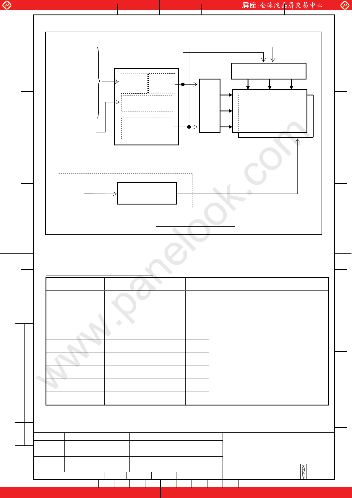
This specification is applied to the 19-inch SXGA supported TFT-LCD module.
㪘㩷
www.panelook.com
2–1 Product Name :
2-2 Model Number : NA19020-C961
㪙㩷
This LCD module has a TFT active matrix type liquid crystal panel 1280x1024 pixels, and
diagonal size of 48cm(19-inch). This LCD has a LVDS dual interface and can display
16,777,216 colors.
The power supply of this LCD module is +5V DC
voltage
.
This module has the characteristics for applying TCO’99.
㪚㩷 㪚
This LCD module consists of a color TFT-LCD panel that is mounted with TFT driver ICs
a cold-cathode fluorescent tube back-light.
and
The inverter for the back-light is not included.
㪛㩷
Figure 4-1 shows a block diagram of this LCD module.
DATE DOCUMENT CONTROL SECTION
EDIT
DESIG.
DATE
DESIG. DESCRIPTION
CHECK
APPR.
CHECK
APPR.
㪈㩷
One step solution for LCD / PDP / OLED panel application: Datasheet, inventory and accessory!
TITLE
NA19020-C961
DRAW. NO.
Tech Bes LCD-00199
FUJITSU DISPLAY TECHNOLOGIES
CORPORATION
㪛
㪜
CUST.
SHEET
3
/
www.panelook.com
Page 5
Global LCD Panel Exchange Center
5. MECHANICAL SPECIFICATIONS
Input signals (LVDS Dual)
www.panelook.com
RXE0㪂
RXE0㪄㩷 㩷
RXE1㪂㩷 㩷
RXE1㪄
RXE2㪂
RXE2㪄㩷 㩷
RXE3㪂
RXE3㪄㩷 㩷
RXEC㪂
RXEC㪄㩷 㩷
Vcc
(+5V)
LVDS
Receiver
DC/DC converter
Bias voltage
Supply circuit
Internal
Circuit
Data driver
Gate
Driver
TFT color LCD panel
1280x3(RGB)x1024
㩷
Back-light
(4 CCFL)
㪘㩷
㪙㩷
RXO0㪂
RXO0㪄㩷 㩷
RXO1㪂㩷 㩷
RXO1㪄
RXO2㪂
RXO2㪄㩷 㩷
RXO3㪂
RXO3㪄㩷 㩷
RXOC㪂
RXOC㪄㩷 㩷
PD
(Separate)
Power
supply
㪚㩷 㪚
Inverter circuit
Figure 4-1 Block Diagram
Ta ble 5-1 shows the mechanical specifications of this L CD mod ule.
Table 5-1 Mechanical Specifications
Item Specifications Unit Remark
㪛㩷
Dimensions
Display
Resolution
Display Dot Area
Dot Pitch
Aspect Ratio
Pixel
Weight 3,000 MAX
FG-SG Short circuit —
414x335x23(TYP.)
(1280x3)x1024
376.32x301.056
(0.098x3)x0.294
1:1 —
mm
—
mm
mm
g
Edge type back-light is used.
(φ2.6 CCFLx4)
Without inverter.
For details on dimensions,
see dimensional outlin e drawing.
(Figure 19-1,2,3)
Excluding inverter.
㪛
㪜
DATE DOCUMENT CONTROL SECTION
TITLE
DRAW. NO.
NA19020-C961
Tech Bes LCD-00199
EDIT
DESIG.
DATE
DESIG. DESCRIPTION
CHECK
APPR.
CHECK
APPR.
FUJITSU DISPLAY TECHNOLOGIES
CORPORATION
㪈㩷
One step solution for LCD / PDP / OLED panel application: Datasheet, inventory and accessory!
CUST.
SHEET
4
/
www.panelook.com
Page 6
Global LCD Panel Exchange Center
6. ABSOLUTE MAXIMUM RATING
7. RECOMMENDED OPERATING CONDITIONS
Table 6-1 shows the absolute maximum rating of this LCD module.
www.panelook.com
㪘㩷
Table 6-1 Absolute Maximum Rating
Item Symbol Condition MIN. TYP. MAX. Unit
Supply Voltage VCC Ta=25ºC –0.3 — 6.0 V
Input Signal Voltage
(LVDS signal, PD)
Ta=25ºC –0.3 — 3.6 V
V
IN
㪙㩷
Ta ble 7-1 shows the recommended operating conditio ns of thi s LCD module.
Ta ble 7-1 Recommended Operating Conditions
Item Symbol MIN. TYP. MAX. Unit
Supply V o ltage( Logic) V
CC
㪚㩷 㪚
Ripple Voltage V
CC
V
RP
4.75 — 5.25 V
— — 0.1 V
㩷
㩷
㩷
㪛㩷
㩷
㩷
㩷
㩷
㩷
㩷
㩷
㩷
㩷
㩷
㩷
㩷
㩷
DATE DOCUMENT CONTROL SECTION
㩷
㩷
TITLE
DRAW. NO.
NA19020-C961
Tech Bes LCD-00199
EDIT
DESIG.
DATE
DESIG. DESCRIPTION
CHECK
APPR.
CHECK
APPR.
FUJITSU DISPLAY TECHNOLOGIES
CORPORATION
㪈㩷
One step solution for LCD / PDP / OLED panel application: Datasheet, inventory and accessory!
㪛
㪜
CUST.
SHEET
5
/
www.panelook.com
Page 7
Global LCD Panel Exchange Center
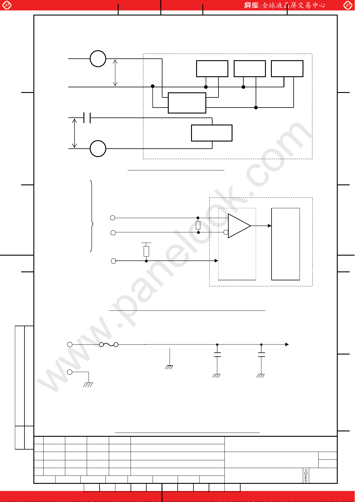
8. ELECTRICAL SPECIFICATIONS
Table 8-1 shows the electrical specifications of this LCD module. Figure 8-1 shows the
㪘㩷
measurement circuit. Figure 8-2(A) shows the equivalent circuit of the logic signal input area.
Figure 8-2(B) shows the equivalent ci rcuit of the su p ply voltage Input area.
Table 8-1 Electrical Specifications
www.panelook.com
Item Symbol Condition MIN. TYP. MAX. Unit
Differential-input
Voltage (Hign)
V
IH
— — 100 mV
Remark
VCM=+1.2V
Differential-input
Voltage (Low)
㪙㩷
Input PD Voltage (High) V
Input PD Voltage (Low) V
V
IL
IHPD
0 — 0.8 V
ILPD
–100 — — mV
2.0 — 3.3 V
VCC=+5.0±0.25V
V
=0V
Supply Current I
CC
SS
DCLK=54MHz
— 800 1,500 mA *1
Ta=25º C
Supply Rush Current I
SCC
— — 3.5 A
*2
Supply Rush Current
Duration(1.5A excess)
㪚㩷 㪚
BACK
CCFL T urn on
Voltage
T
SCC
V
— — 1 ms
fL=50kHz,Ta=25ºC — 1,400 1,600
S
Vrms
fL=50kHz,Ta=0ºC — — 1,600
LIGHT
Lighting Voltage V
L
fL=50kHz
I
=7mA
L
— 750 — Vrms
㪛㩷
Lighting Frequency f
(*3)
T u be C urrent I
VL=750Vrms 40 50 60 kHz
L
L
fL=50kHz
V
=750Vrms
L
4 7 8
(*1) Typi cal current situation : Color bar pattern. Vcc=5.0V
Maximum current situation : White pattern. Vcc=4.75V
Without rush curre nt.
(*2) These items prescribe the rush current for starting internal DC/DC.
Charging current to capacitors of Vcc is not prescribed.
(*3) Back-light specificat ions are valid when using a suita ble inverter such as the
FLCV-13
(*4) T u be current (I
) shows the value of the current that is consumed at one lamp.
L
This LCD module has 4 lamps. Each 2 lamps are placed at upper side and
lower side of the display.
2 lamps is connected in parallel. Each low voltage terminals are connected with separate
cable to Back-light connecter.
DATE DOCUMENT CONTROL SECTION
㩷
㩷 㩷
EDIT
DESIG.
DATE
DESIG. DESCRIPTION
CHECK
APPR.
CHECK
APPR.
TITLE
NA19020-C961
DRAW. NO.
Tech Bes LCD-00199
FUJITSU DISPLAY TECHNOLOGIES
CORPORATION
㪈㩷
One step solution for LCD / PDP / OLED panel application: Datasheet, inventory and accessory!
mArms
*4
㪛
㪜
CUST.
SHEET
6
/
www.panelook.com
Page 8
Global LCD Panel Exchange Center
V
㩷
Measurement circuit is based on Figure 8-1.
www.panelook.com
㪘㩷
+5V
GND
Icc
Vcc
Logic Analog Driver
DC/DC
C
L
Converter
AC
㪙㩷
GND
Vs
䌉
L
Back-light
LCD module
Figure 8-1 Measurement circuit
Input signals (LVDS Dual)
RXO0㪂
RXO0㪄㩷 㩷
RXO1㪂㩷 㩷
RXO1㪄
RXO2㪂
RXO2㪄㩷 㩷
㪚㩷 㪚
RXO3㪂
RXO3㪄㩷 㩷
RXOC㪂
RXOC㪄㩷 㩷
RXE0㪂
RXE0㪄㩷 㩷
RXE1㪂㩷 㩷
RXE1㪄
RXE2㪂
RXE2㪄㩷 㩷
RXE3㪂
RXE3㪄㩷 㩷
RXEC㪂
RXEC㪄㩷 㩷
+
−
Differential
Input
+3.3V
100
10kΩ(pull-up)
LVDS Receiver
Ω
Internal
circuit
PD
LVDS Receiver : DS90CF386(National Semiconductor Corp. or equivale nt)
㪛㩷
Figure 8-2(A) Equivalent circuit of logic signal Input
Fuse
cc
EMI Filter
䋨
义
100pF
Internal
Circuit
10μF
GND
FG
Frame ground
(
)
Fuse : F0603C3R00FWTRM 3.0A (Kyocera Corp. or equivalent)
EMI Filter : SGM20C1E332 (Sumitomo Metal Inc. or equival ent)
Figure 8-2(B) Equivalent circuit of power supply
㪛
㪜
DATE DOCUMENT CONTROL SECTION
TITLE
NA19020-C961
DRAW. NO.
Tech Bes LCD-00199
EDIT
DESIG.
DATE
DESIG. DESCRIPTION
CHECK
APPR.
CHECK
APPR.
FUJITSU DISPLAY TECHNOLOGIES
CORPORATION
㪈㩷
One step solution for LCD / PDP / OLED panel application: Datasheet, inventory and accessory!
SHEET
www.panelook.com
7
/
CUST.
Page 9
Global LCD Panel Exchange Center
9. OPTICAL SPECIFICATIONS
Ta ble 9-1 shows the optical specifications of this LCD module.
www.panelook.com
㪘㩷
Table 9-1 Optical Specifications
Ta=25˚C, Signal timing=Typ.
Specifications Remark
Item Symbol Condition
MIN. TYP. MAX.
Visual
Angle
Horizontal
Vertical
All Direction
Contrast Ratio CR
㪙㩷
Response
Time(ON)
(B→W)
Response
Time(OFF)
(W→B)
Brightness
Brightness
Uniformity
㪚㩷 㪚
Chromaticity
W
θ
θ
t
t
△I
L,R
U,D
θ
on
off
I
x
y
CR≧10
θ
L,R,U,D
θ
L,R,
U,D
=0
°
θ
L,R,
U,D
=0
°
2
○
θ
L,R,U,D
=5V
V
CC
=7mA
I
L
fL=50kHz
R*,G*,B* Signal
=All “H”
R
(x,y)
G
B
=0
U,D
L,R
=0
°
°
85 — — deg
85 — — deg
θ
θ
— 80 — deg
=0
°
Ta=25˚C
Ta=0
Ta=25˚C
Ta=0
=0
°
˚C
˚C
400 600 — —
— 15 30 ms
— 50 100 ms
— 10 25 ms
— 50 100 ms
50
200
2
70 — —
0.293
.323 0.353
0
0.307 0.337 0.367
Red ( 0.648 , 0.346 ) Typ.
Green ( 0.292 , 0.602 ) Typ.
Blue ( 0.150 , 0.130 ) Typ.
Unit
cd/m
%
—
—
2
Note
(1)(2)
(3)(5)
(6)
White/
Black
(1)(2)
(3)(5)
(1)
(4)
(5)
(1)(5)
(1)(5)
White
(7)
*1
(1)
(5)
LCD Panel Type TFT Color
㪛㩷
Display Mode Normaly Black
Wide Viewing Angle Technology MVA
Optimum Viewing Angle — (symmentry) (6)
Display Color 16,777,216 (8-bit color)
Color of non-display area Black
Surface Treatment
Anti-glare
(Haze value:(25%),2H)
(*1) Value at 15〜20 minutes after lighting on.
2
(Note) 䊶CS-1000 (MINOLTA Co., Ltd.) Field=1°, L=500mm
○
䊶
Back-light current = 7mA, Dark room condition(1 lux or less)
Be carefull that the luminance meter, which you use, may not be able to get correct brightenss
if it’s no set correctly.
DATE DOCUMENT CONTROL SECTION
02 20031010 Add condition, revised note
EDIT
DESIG.
DATE
DESIG. DESCRIPTION
CHECK
APPR.
CHECK
APPR.
TITLE
NA19020-C961
DRAW. NO.
Tech Bes LCD-00199
FUJITSU DISPLAY TECHNOLOGIES
CORPORATION
㪈㩷
One step solution for LCD / PDP / OLED panel application: Datasheet, inventory and accessory!
㪛
㪜
CUST.
SHEET
8
/
www.panelook.com
Page 10
Global LCD Panel Exchange Center
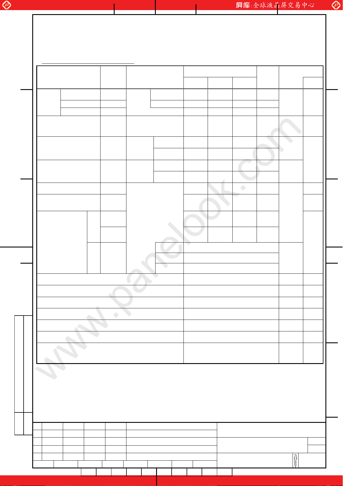
Note 1) Definition of Viewing Angle (1)
www.panelook.com
Based on Figure 9-1.
*0㫦(Front)
㪘㩷
㱔
䌒
㱔
㩷㩷㩷㩷㩷㩷㩷㩷㩷㩷Y+
Top (12 o’clock Direction)
LCD module
䌌
㱔
㱔
㪬
䌄
㩷㩷㩷㩷㩷㩷㩷㩷㩷㩷X+
Right (3 o’clock Directio n)
㪙㩷
㩷㩷㩷㩷㩷㩷㩷㩷㩷㩷Y-
㩷㩷㩷㩷㩷㩷㩷㩷㩷㩷X-
Left (9 o’clock Direction)
䋪→㱔
䋽䋰㫦䋬㱔D䋽䋰㫦䋬㱔L䋽䋰㫦䋬㱔R䋽䋰㫦
U
㪙㫆㫋㫋㫆㫄㩷㩿㪍㩷㫆’㪺㫃㫆㪺㫂㩷㪛㫀㫉㪼㪺㫋㫀㫆㫅㪀
Figure 9-1 Definition of Viewing Angle (1)
Note 2) Definition of Viewing Angle (2)
㪚㩷 㪚
Based on Figure 9-2.
㱔
㱔
㪤㪠㪥
㪫㪰㪧
㱔
㪤㪘㪯
Display Surface
㪛㩷
Display Surface
Figure 9-2 Definition of Viewing Angle (2)
Note 3) Definition of Contrast Ratio (CR)
Determined by Formula (1) based on
Figure 9-3 Voltage-Brightness
characteristics.
䌌
(Brightness at white)
W
=
(Brightness at black) 㵺㵺(1)
䌌
䌂
Figure 9-3 Voltage-Brightness Characteristics
L
Brightness
䌛L䌝
L
B
0
W
㱔
㩷 㪔㪇㫦
0
㪣㪃㪩㪃㪬㪃㪛
Black
Panel Drive Voltage 䌛䌖䌝
㪛
White
㪜
DATE DOCUMENT CONTROL SECTION
㩷
㩷
EDIT
DESIG.
DATE
DESIG. DESCRIPTION
CHECK
APPR.
CHECK
APPR.
TITLE
NA19020-C961
DRAW. NO.
Tech Bes LCD-00199
FUJITSU DISPLAY TECHNOLOGIES
CORPORATION
㪈㩷
One step solution for LCD / PDP / OLED panel application: Datasheet, inventory and accessory!
CUST.
SHEET
9
/
www.panelook.com
Page 11
Global LCD Panel Exchange Center
p
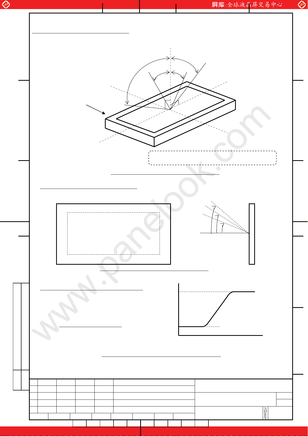
Note 4) Definition of Response Time
Based on Figure 9-4.
www.panelook.com
㪘㩷
Drive signal of
LCD panel
ON
OFF
Non-select status Select status Non-select status
100%
Relative
Brightnes
㪙㩷
90%
White
10%
0%
Black
ON Res
䌴
䌴
on
off
onse Time OFF Response Time
Black
Figure 9-4 Definition of Response Ti m e
㪚㩷 㪚
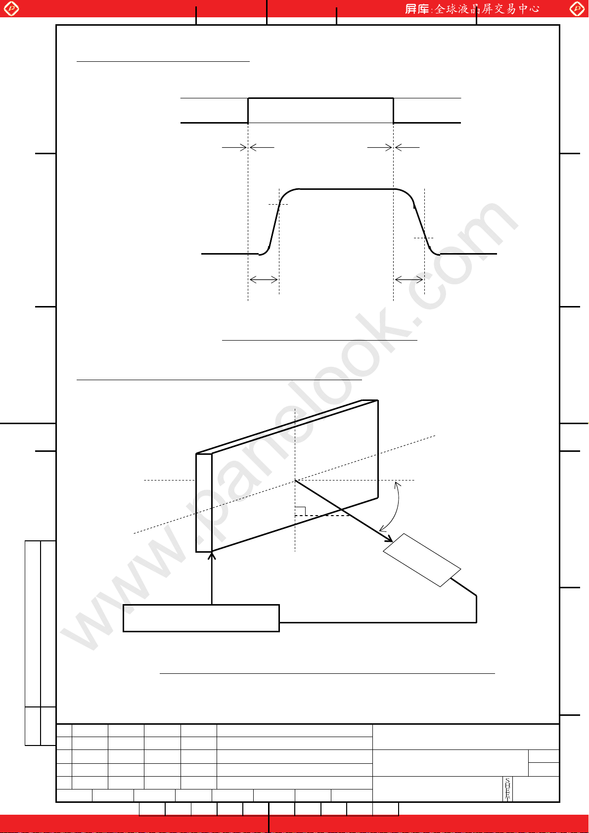
Note 5) Contrast Ratio and Response Measurement System
㪛㩷
Based on Figure 9-5.
-
Z
-
X
Drive and Measurement System
Figure 9-5 Contrast Ratio and Response Time Measurement System
+
Y
+
X
+
Z
Brightness Meter or
㱔
-
Y
Luminance colorimeter
(with luminosity
correction function)㩷
㪛
㪜
DATE DOCUMENT CONTROL SECTION
㩷
EDIT
DESIG.
DATE
DESIG. DESCRIPTION
CHECK
APPR.
CHECK
APPR.
TITLE
NA19020-C961
DRAW. NO.
Tech Bes LCD-00199
FUJITSU DISPLAY TECHNOLOGIES
CORPORATION
㪈㩷
One step solution for LCD / PDP / OLED panel application: Datasheet, inventory and accessory!
CUST.
SHEET
10
/
www.panelook.com
Page 12

Global LCD Panel Exchange Center
㩷
㩷
㩷
㩷
Note 6) Definition of Optimum Viewing Angle
www.panelook.com
㪘㩷
MAX
Contrast
Ratio
10
㪙㩷
䋨-䋩
6 o’clock
Viewing Angle㱔
←
0
䋨+䋩
12 o’clock
→
Figure 9-6 Definition of Viewing Angle
Note 7) Definition of Brightness Uniformity
Brightness uniformity is defined by the following formula.
Brightness (I1䌾I9) art measured at the following 9 points (㽲䌾㽺) on the display area
that is shown in Figure 9-7.
㪚㩷 㪚
䌼Min. In䌼
Brightness Uniformity ( 䂦L) 䋽 㬍 100 (%) , n = 1 to 9
䌼Max. In䌼
192 640 1088 Dot
㽲㩷
㽵
㽸
154
㪛㩷
㽳㩷
㽴
㽶
㽷
㽹
㽺
512
870
Note) Each measurement point (㽲䌾㽺) defines the cent er spot of view of Brightness Meter.
The tolerance of measurement position is㫧3mm.
Figure 9-7 Measurement Points
DATE DOCUMENT CONTROL SECTION
EDIT
DESIG.
DATE
DESIG. DESCRIPTION
CHECK
㪈㩷
One step solution for LCD / PDP / OLED panel application: Datasheet, inventory and accessory!
APPR.
CHECK
APPR.
TITLE
NA19020-C961
DRAW. NO.
Tech Bes LCD-00199
FUJITSU DISPLAY TECHNOLOGIES
CORPORATION
㪛
㪜
CUST.
SHEET
11
/
www.panelook.com
Page 13

Global LCD Panel Exchange Center
10. INTERFACE SPECIFICATIONS
www.panelook.com
10-1 Signal descriptions
㪘㩷
㪙㩷
㪚㩷 㪚
㪛㩷
FI-X30H (Wire type)
FI-X30C (Coaxial cable type)
Ta ble 10-1 shows the description and configuration of interface signals (CN1).
Ta ble 10-1 Interface signals (CN 1)
Pin No. Symbol I/O Function
RxO0
1
2 RxO0+
3
4 RxO1+
5
6 RxO2+
7 GND
8
-I
RxO1
- I
RxO2
-I
―Ground
RxOC
-I
Negative differential input
I
Positive different ial in pu t
Negative differential input
I
Positive different ial in pu t
Negative differential input
I
Positive different ial in pu t
Negative differential input
9 RxOC+ I Positive different ial in put
RxO3
10
-
I Negative differential inp ut
11 RxO3+ I Positive different ial in pu t
RxE0
RxE1
-
I Negative differential inp ut
I
Positive different ial in pu t
―Ground
-
I Negative differential inp ut
12
13 RxE0+
14 GND
15
16 RxE1+ I Positive different ial in put
17 GND
RxE2
18
-
―Ground
I
Negative differential input
19 RxE2+ I Positive different ial in put
RxEC
20
21 RxEC+
22
23
24 GND
25 TST
26 PD
27
28 Vcc
29 Vcc
30 Vcc
-
RxE3
- I
RxE3+
TST
I Negative differential inp ut
I
Positive different ial in pu t
Negative differential input
I Positive different ial in put
―Ground
―
Test pin *1
I
LVDS Core Power Down
―
Test pin *1
―
+5V power supply
―
+5V power supply
―
+5V power supply
Connector : FI-X30S-HF(Japan A viation Electronics)
User’s connector : FI-X30M (FPC type) (Japan Aviation Electronics)
*1: Keep open. (Internal test use only.)
2
*2: When using a connect or other t han the recommended one , a defect in the initial stage or
䂾
a problem concerning long term reliabil ity may occur.
㪛
㪜
DATE DOCUMENT CONTROL SECTION
02
20031010 Add *2.
EDIT
DESIG.
DATE
DESIG. DESCRIPTION
CHECK
APPR.
CHECK
APPR.
TITLE
NA19020-C961
DRAW. NO.
Tech Bes LCD-00199
FUJITSU DISPLAY TECHNOLOGIES
CORPORATION
㪈㩷
One step solution for LCD / PDP / OLED panel application: Datasheet, inventory and accessory!
CUST.
SHEET
12
/
www.panelook.com
Page 14

Global LCD Panel Exchange Center
www.panelook.com
10-2 LVDS Data Assignment
Table 10-2 shows the LVDS Data Assignment.
Table 10-2 LVDS Data Assignment
㪘㩷
Input signal *1
RO2
RO3
RO4
RO5
RO6
RO7
GO2
GO3
㪙㩷
LVDS
Odd
㪚㩷 㪚
㪛㩷
LVDS
Even
GO4
GO5
GO6
GO7
BO2
BO3
BO4
BO5
BO6
BO7
RSVD
RSVD
ENAB
RO0
RO1
GO0
GO1
BO0
BO1
RSVD
DCLK 31 TxCLK IN
RE2
RE3
RE4
RE5
RE6
RE7
GE2
GE3
GE4
GE5
GE6
GE7
BE2
BE3
BE4
BE5
BE6
BE7
RSVD
RSVD
RSVD
RE0
RE1
GE0
GE1
BE0
BE1
RSVD
DCLK 31 TxCLK IN
Transmitter
DS90CF383,C385
Interface connector
pin INPUT System side
TxIN0
51
TxIN1
52
54
55
56
11
12
14
15
19
20
22
23
24
27
28
30
50
10
16
18
25
51
52
54
55
56
11
12
14
15
19
20
22
23
24
27
28
30
50
10
16
18
25
3
4
6
7
2
8
3
4
6
7
2
8
TxIN2
TxIN3
TxIN4
TxIN6
TxIN7
TxIN8
TxIN9
TxIN12
TxIN13
TxIN14
TxIN15
TxIN18
TxIN19
TxIN20
TxIN21
TxIN22
TxIN24
TxIN25
TxIN26
TxIN27
TxIN5
TxIN10
TxIN11
TxIN16
TxIN17
TxIN23
TxIN0
TxIN1
TxIN2
TxIN3
TxIN4
TxIN6
TxIN7
TxIN8
TxIN9
TxIN12
TxIN13
TxIN14
TxIN15
TxIN18
TxIN19
TxIN20
TxIN21
TxIN22
TxIN24
TxIN25
TxIN26
TxIN27
TxIN5
TxIN10
TxIN11
TxIN16
TxIN17
TxIN23
Tx OUT0+
Tx OUT0
Tx OUT1+
Tx OUT1
Tx OUT2+
Tx OUT2
Tx OUT3+
Tx OUT3
TxCLK OUT+
TxCLK OUT
Tx OUT0+
Tx OUT0
Tx OUT1+
Tx OUT1
Tx OUT2+
Tx OUT2
Tx OUT3+
Tx OUT3
TxCLK OUT+
TxCLK OUT
-
-
-
-
-
-
-
-
-
-
LCD module
pin
RxO0+
2
RxO0
1
RxO1+
4
RxO1
3
RxO2+
6
RxO2
5
9
8
RxO3+
RxO3
RxCLK IN+
RxCLK IN
RxE0+
RxE0
RxE1+
RxE1
RxE2+
RxE2
RxE3+
RxE3
RxCLK IN+
RxCLK IN
11
10
13
12
16
15
19
18
23
22
21
20
-
-
-
-
-
-
-
-
-
-
Receiver
DS90CF386
pin OUTPUT
RxOUT0
27
RxOUT1
29
RxOUT2
30
RxOUT3
32
RxOUT4
33
RxOUT6
35
RxOUT7
37
RxOUT8
38
RxOUT9
39
RxOUT12
43
RxOUT13
45
RxOUT14
46
RxOUT15
47
RxOUT18
51
RxOUT19
53
RxOUT20
54
RxOUT21
55
RxOUT22
1
RxOUT24
3
RxOUT25
5
RxOUT26
6
RxOUT27
7
RxOUT5
34
RxOUT10
41
RxOUT11
42
RxOUT16
49
RxOUT17
50
RxOUT23
2
26 RxCLK OUT DCLK
RxOUT0
27
RxOUT1
29
RxOUT2
30
RxOUT3
32
RxOUT4
33
RxOUT6
35
RxOUT7
37
RxOUT8
38
RxOUT9
39
RxOUT12
43
RxOUT13
45
RxOUT14
46
RxOUT15
47
RxOUT18
51
RxOUT19
53
RxOUT20
54
RxOUT21
55
RxOUT22
1
RxOUT24
3
RxOUT25
5
RxOUT26
6
RxOUT27
7
RxOUT5
34
RxOUT10
41
RxOUT11
42
RxOUT16
49
RxOUT17
50
RxOUT23
2
26 RxCLK OUT Not use
LCD
Control
input
RO2
RO3
RO4
RO5
RO6
RO7
GO2
GO3
GO4
GO5
GO6
GO7
BO2
BO3
BO4
BO5
BO6
BO7
Not use
Not use
ENAB
RO0
RO1
GO0
GO1
BO0
BO1
No
t use
RE2
RE3
RE4
RE5
RE6
RE7
GE2
GE3
GE4
GE5
GE6
GE7
BE2
BE3
BE4
BE5
BE6
BE7
Not use
Not use
Not use
RE0
RE1
GE0
GE1
BE0
BE1
Not use
*1 ・RSVD (reserved) pin on a transmitter should be connected with Ground.
㪛
㪜
・Input odd or even data depending on the dis play po sition of the LCD module.
DATE DOCUMENT CONTROL SECTION
TITLE
NA19020-C961
DRAW. NO.
Tech Bes LCD-00199
EDIT
DESIG.
DATE
DESIG. DESCRIPTION
CHECK
APPR.
CHECK
APPR.
FUJITSU DISPLAY TECHNOLOGIES
CORPORATION
㪈㩷
One step solution for LCD / PDP / OLED panel application: Datasheet, inventory and accessory!
CUST.
SHEET
13
/
www.panelook.com
Page 15

Global LCD Panel Exchange Center
:
: : : : : : : : : : : : : : : : : : : : : : : :
:
: : : : : : : : : : : : : : : : : : : : : : : :
:
: : : : : : : : : : : : : : : : : : : : : : : :
:
: : : : : : : : : : : : : : : : : : : : : : : :
:
: : : : : : : : : : : : : : : : : : : : : : : :
:
: : : : : : : : : : : : : : : : : : : : : : : :
:
: : : : : : : : : : : : : : : : : : : : : : : :
:
: : : : : : : : : : : : : : : : : : : : : : : :
:
: : : : : : : : : : : : : : : : : : : : : : : :
10-3 Color Data Assignment
Ta ble 10-3 shows the Color Data Assignment.
㪘㩷
Table 10-3 Color Data Assignment
www.panelook.com
Color
Odd
Even
Black
Blue
Green
Cyan
Red
㪙㩷
Magenta
BasicColor
Yellow
White
Black 0
×
×
1
Red
Ø
Brighter 253
Ø
㪚㩷 㪚
Red 255
Black 0
×
×
254
1
Green
Ø
Brighter 253
Ø
254
Green 255
Black 0
㪛㩷
×
×
1
Blue
Ø
Brighter 253
Ø
254
Blue 255
R Input data
R7 R6 R5 R4 R3 R2 R1 R0
R7 R6 R5 R4 R3 R2 R1 R0
0 0 0 0 0 0 0 0 0 0 0 0 0 0 0 0 0 0 0 0 0 0 0 0
0 0 0 0 0 0 0 0 0 0 0 0 0 0 0 0 1 1 1 1 1 1 1 1
0 0 0 0 0 0 0 0 1 1 1 1 1 1 1 1 0 0 0 0 0 0 0 0
0 0 0 0 0 0 0 0 1 1 1 1 1 1 1 1 1 1 1 1 1 1 1 1
1 1 1 1 1 1 1 1 0 0 0 0 0 0 0 0 0 0 0 0 0 0 0 0
1 1 1 1 1 1 1 1 0 0 0 0 0 0 0 0 1 1 1 1 1 1 1 1
1 1 1 1 1 1 1 1 1 1 1 1 1 1 1 1 0 0 0 0 0 0 0 0
1 1 1 1 1 1 1 1 1 1 1 1 1 1 1 1 1 1 1 1 1 1 1 1
0 0 0 0 0 0 0 0 0 0 0 0 0 0 0 0 0 0 0 0 0 0 0 0
0 0 0 0 0 0 0 1 0 0 0 0 0 0 0 0 0 0 0 0 0 0 0 0
G Input data B Input data
G7 G6 G5 G4 G3 G2 G1 G0 B7 B6 B5 B4 B3 B 2 B1 B0
G7 G6 G5 G4 G3 G2 G1 G0 B7 B6 B5 B4 B3 B 2 B1 B0
1 1 1 1 1 1 0 1 0 0 0 0 0 0 0 0 0 0 0 0 0 0 0 0
1 1 1 1 1 1 1 0 0 0 0 0 0 0 0 0 0 0 0 0 0 0 0 0
1 1 1 1 1 1 1 1 0 0 0 0 0 0 0 0 0 0 0 0 0 0 0 0
0 0 0 0 0 0 0 0 0 0 0 0 0 0 0 0 0 0 0 0 0 0 0 0
0 0 0 0 0 0 0 0 0 0 0 0 0 0 0 1 0 0 0 0 0 0 0 0
0 0 0 0 0 0 0 0 1 1 1 1 1 1 0 1 0 0 0 0 0 0 0 0
0 0 0 0 0 0 0 0 1 1 1 1 1 1 1 0 0 0 0 0 0 0 0 0
0 0 0 0 0 0 0 0 1 1 1 1 1 1 1 1 0 0 0 0 0 0 0 0
0 0 0 0 0 0 0 0 0 0 0 0 0 0 0 0 0 0 0 0 0 0 0 0
0 0 0 0 0 0 0 0 0 0 0 0 0 0 0 0 0 0 0 0 0 0 0 1
0 0 0 0 0 0 0 0 0 0 0 0 0 0 0 0 1 1 1 1 1 1 0 1
0 0 0 0 0 0 0 0 0 0 0 0 0 0 0 0 1 1 1 1 1 1 1 0
0 0 0 0 0 0 0 0 0 0 0 0 0 0 0 0 1 1 1 1 1 1 1 1
Note.1) Definition of gray scale:Color (n)…”n” indicates gray scale level.
Larger number means brighter level.
Note.2) Data; 1:High, 0:Low
㪛
Note 3) Color data consis t of 8 bit red, green and blue data of odd and even number pixel data.
Total data number is 48 signals. This module is able to display 16,777,216 colors because
each red, green and blue data is controlled independently.
DATE DOCUMENT CONTROL SECTION
TITLE
NA19020-C961
DRAW. NO.
Tech Bes LCD-00199
EDIT
DESIG.
DATE
DESIG. DESCRIPTION
CHECK
APPR.
CHECK
APPR.
FUJITSU DISPLAY TECHNOLOGIES
CORPORATION
㪈㩷
One step solution for LCD / PDP / OLED panel application: Datasheet, inventory and accessory!
㪜
CUST.
SHEET
14
/
www.panelook.com
Page 16

Global LCD Panel Exchange Center
10-4 Input Signal Timing
Table 10-4 and Figure 10-1 shows the Input Signal Timing at LVDS transmitter.
www.panelook.com
Table 10-4 Timing Characteristics
㪘㩷
(Ta=0~50˚C, Vcc=5±0.25V)
Item Symbol Min. Typ. Max. Unit Remark
㪙㩷
DCLK
signal
(Clock)
DCLK-Data
Timing
ENAB
signal
Period
Frequency
Duty
High time
Low time
Setup time
Hold time
Horizontal Period
Hor. Period (1)
Hor. Period (2)
Hor. Display period
Vertical Period
Ver. Frequency
Ver. Display period
Tc
1/Tc
Tch/Tc
TclkH
TclkL
Tset
Thold
Th
Th
Th
Thd
Tv
1/Tv
Tvd
16.7
40
45
5.0
5.0
3
5
5500/Tc+450
14.0
10.6
640
*1
1028
50
1024
18.5
54
50
—
—
—
—
844
15.6
15.6
640
1066
60
1024
25.0
60
55
—
—
—
—
887
—
—
640
1088
69
1024
*1
*1
ns
MHz
%
ns
ns
ns
ns
DCLK
µs
µs
DCLK
Th
Hz
Th
*4
*4
*2
16.67ms
*2
Data-ENAB timing Tdn — 0 — DCLK *3
*1)•horizontal display position is specified by the rise of ENAB.
The data latched at falling edge of DCLK after rise of ENAB is displayed at the left edge of the display area.
•Vertical display position is specified by the rise of ENAB after low level continuation over 2048 DCLK.
㪚㩷 㪚
The data latched at the rise of ENAB is displayed at the top line of the display area.
*2)•If the “High” level period of ENAB is less than 640 DCLK or the number of ENAB in a frame period (Tv) is
less than 1024, black color is displayed at the rest of the display area.
*3)•If ENAB does not synchronize with the effective display data, the display position does not fit to the
display area.
*4)•Hor. Period (2) shows the operating range whe re internal circuit can work correctly.
・When ENAB signal is out of Hor. Period (1), the display quality may deteriorate.
㪛㩷
㪛
㪜
DATE DOCUMENT CONTROL SECTION
TITLE
NA19020-C961
DRAW. NO.
Tech Bes LCD-00199
EDIT
DESIG.
DATE
DESIG. DESCRIPTION
CHECK
APPR.
CHECK
APPR.
FUJITSU DISPLAY TECHNOLOGIES
CORPORATION
㪈㩷
One step solution for LCD / PDP / OLED panel application: Datasheet, inventory and accessory!
CUST.
SHEET
15
/
www.panelook.com
Page 17

Global LCD Panel Exchange Center
㪘㩷
DCLK
ENAB
RO7-0, RE7-0
GO7-0, GE7-0
BO7-0, BE7-0
㪙㩷
RO7-0, RE7-0
GO7-0, GE7-0
BO7-0, BE7-0
ENAB
www.panelook.com
Tc
TclkL
0.9V
Tc1 Tset
Tclk
2.3V
Tch
1.65
Thold
Th
Thd
2.3V
0.9V
RO7-0, RE7-0
C001 C1024
GO7-0, GE7-0
BO7-0, BE7-0
㪚㩷 㪚
ENAB
Tvd
Tv
Tc
DCLK
㪛㩷
0001
RO7-0, RE7-0
0003
0005
0007
0009
0011
1267
1269
1273 1277
1271
1275
1279
GO7-0, GE7-0
BO7-0, BE7-0
ENAB
0002
0004
0006
0008
0010
0012
1268
1270
1272
1274
1276
1278
1280
Tdn Tdn
㪛
Figure 10-1 Input Signal Timing Chart
DATE DOCUMENT CONTROL SECTION
TITLE
DRAW. NO.
NA19020-C961
Tech Bes LCD - 00199
EDIT
DESIG.
DATE
DESIG. DESCRIPTION
CHECK
APPR.
CHECK
APPR.
FUJITSU DISPLAY TECHNOLOGIES
CORPORATION
㪈㩷
One step solution for LCD / PDP / OLED panel application: Datasheet, inventory and accessory!
㪜
CUST.
SHEET
16
/
www.panelook.com
Page 18

Global LCD Panel Exchange Center
)
10-5 Correspondence between Data an d D isplay Position
Figure 10-2 shows the C orrespondence between D ata and Display Position.
㪘㩷
www.panelook.com
S3839 S3840
GE
1280BE1280
C001
S0001 S0002 S0003 S0004 S0005 S0006 S0007
RO
0001GO0001BO0001RE0002GE0002BE0002RO0003GO0003
㪙㩷
C1024
RO
0001GO0001BO0001RE0002GE0002BE0002RO0003GO0003
GE
1280BE1280
Figure 10-2 Correspondence Data and Display Position
㪚㩷 㪚
10-6 Power Supply Sequence
The sequence of input signals and On/Off of the power supply of this LCD module
should be in the specifica tion shown in Figure 10-3 to prevent latch-up of the
driver ICs and DC driving of the LCD panel.
Vcc
㪛㩷
ON
4.75V
OFF
(0V)
PD
LVDS
Differential
Input
H
Tri-state
L
T1㻡20ms
T2
0ms㻡T2㻡40ms
Inputs should be in a range of the spec. of the LVDS.
0ms㻡T3
90%
10%
2.0V
亖
DCLK should be in a range of
the spec.(Frequency etc.䋩of
the LCD.
㩷㩷㩷㩷㩷㩷*Note : PD input can be set open, if it is not used.
Figure 10-3 Power Supply Sequence
T4㻡20ms(Voltage descent
亖
4.75V
亖
(4.5V)
T6㻡20ms
亖
0ms㻡T5㻡40ms
4.75V
0.5V
0.1s㻡T7
Tri-state
4.75V
㪛
㪜
DATE DOCUMENT CONTROL SECTION
TITLE
DRAW. NO.
NA19020-C961
Tech Bes LCD - 00199
EDIT
DESIG.
DATE
DESIG. DESCRIPTION
CHECK
APPR.
CHECK
APPR.
FUJITSU DISPLAY TECHNOLOGIES
CORPORATION
㪈㩷
One step solution for LCD / PDP / OLED panel application: Datasheet, inventory and accessory!
CUST.
SHEET
17
/
www.panelook.com
Page 19

Global LCD Panel Exchange Center
11. BACK-LIGHT SPECIFICATIONS
㪘㩷
11-1 Pin configuration for Back-light
Ta ble 11-1 shows the description and Pin assignment of the connectors
(CN-A to D) for the Back-light of this LCD module.
Table 11-1 Pin Assignment of CN-A to CN-D
www.panelook.com
㪙㩷
Pin
№
CN-A CN-B CN-C CN-D
1
V
1
L
2 — — — — — —
V
L
Signal
2
V
Function Cable color
4
Power supply
Pink
3
L
V
L
3 GND GND GND GND Ground White or Blue
Connector : Housing : BHR-03VS-1
Contact : SBH-001T-P0.5
User’s Connector : Post with base: SM02(8.0)B-BHS-1-TB
Supplier : Japan Solderless Terminal Trading Company LTD. (J.S.T.)
11-2 Life
The life of the back-light is a minim um of 50,000 hours at the following conditions.
㪚㩷 㪚
(1) Working conditions
Ambient temperature: 25±5
①
Tube current (I
②
) : (7mA or less)
L
℃
(2) Definition of life
Brightness become s 50% or less than the minimum brightness value shown in Table 9-1.
①
The lamp cannot be lit by the minimum val ue of the breakdown voltage(1760Vrms)
②
shown in Tab le 8-1.
Flashing.
③
㪛㩷
11-3 Lamp assembly set (for replacement)
Lamp assembly set(with charge)is prepared for replacing old lamp to new one.
This set consists of a upp er lamp assembly and a l o w er lamp assembly.
㪛
Type number : FLCL-20
Drawing No. : NA19020-5906
Minimum order qty. unit : 20 pcs.
DATE DOCUMENT CONTROL SECTION
TITLE
DRAW. NO.
NA19020-C961
Tech Bes LCD - 00199
EDIT
DESIG.
DATE
DESIG. DESCRIPTION
CHECK
APPR.
CHECK
APPR.
FUJITSU DISPLAY TECHNOLOGIES
CORPORATION
㪈㩷
One step solution for LCD / PDP / OLED panel application: Datasheet, inventory and accessory!
㪜
CUST.
SHEET
18
/
www.panelook.com
Page 20

Global LCD Panel Exchange Center
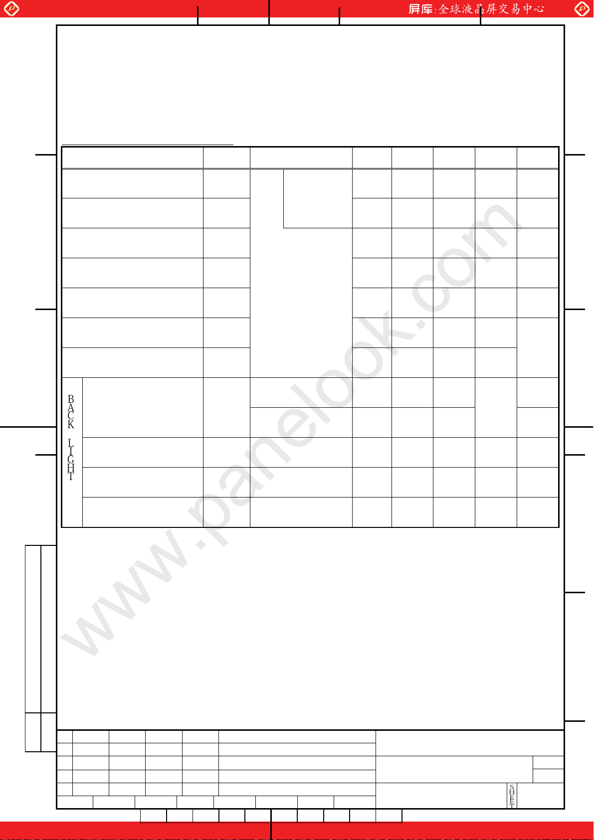
12. APPEARANCE SPECIFICATIONS
g
12-1 Appearance
www.panelook.com
㪘㩷
No. Item
Jud
ment method and standard
1 Bright spot (high and Low) < 8 dots (Note 1 )
Bright spot connection
2
(high and Low)
2 dots connection <
3 dots connection <
2 pair (Note 1)
1 pair
3 Total of bright spot < 8 dots
4 Dark spot < 10 dots (Note 2)
3 pair (Note 2)
1 pair
㪙㩷
5 Dark spot connection
2 dots connection <
3 dots connection <
6 Total of dark sp ot < 10 dots (Note 2)
7 Total of dot defect < 18 dots
8 Distance of dot defect > 2mm
D <0.3 Ignore
9 Black / white spot
0.3< D <0.6 N <5
0.6< D <0.9 N <2 ( Distance >100mm )
0.9< D 0
10 Mura Ignore
㪚㩷 㪚
D:Average diameter [mm], W:Width [mm], L:Length [mm], S=(bright spot size)/(dot size)
㪛㩷
DATE DOCUMENT CONTROL SECTION
20031010 Add this page.
02
EDIT
DESIG.
DATE
DESIG. DESCRIPTION
CHECK
APPR.
CHECK
APPR.
TITLE
DRAW. NO.
NA19020-C961
Tech Bes LCD - 00199
FUJITSU DISPLAY TECHNOLOGIES
CORPORATION
㪈㩷
One step solution for LCD / PDP / OLED panel application: Datasheet, inventory and accessory!
㪛
㪜
CUST.
SHEET
19
/
www.panelook.com
Page 21

Global LCD Panel Exchange Center
12-2 Dot defects (Bright spots, Dark spots)
www.panelook.com
㪘㩷
12-2-1 Zone
· Inside display dot are a (376. 32×301.056mm)
· Display dot area means active area.
· One pixel consists of 3 dots (red, green and blue).
· Foreign particle and scratch unharmful to display image, such as the foreign particle
under polarizer film but outside of the display area and scratch on metal bezel, backlight
module or polarizer film out of the display area, etc., are not counted.
12-2-2 Bright spots
㪙㩷
(1) Bright spots by the defect of TFT.
· Visible under bias of 2% ND filter................................... High bright spot R•G
· Visible under 5% but invisible under 2% ND filter........ Low bright spot R•G•B
· Invisible under bias of 5% ND filter................................ Not counted
(2) Bright spots by the light passing th rough tears, breaks, etc in color filt er.
· Exceed size of a half dot ................................................... High bright spot
· A half dot or less................................................................ Not counted
(3) Bright spots by the light passing through tear s, breaks, etc in chromium mask.
· Exceed 50Pm..................................................................... High bright spot
· 50Pm or less ..................................................................... Not counted
㪚㩷 㪚
㪛㩷
12-2-3 Test condition
· Inspector must observe the LCD screen from the normal direction un der the illumination by
a single 20W fluorescent lamp. The distance betw een the LCD screen and the inspector
should be a height of 50cm above the w orktable.
The vertical illuminance is 300 to 600lux (reference value).
· Bright spot should be counted under entire black screen.
· Dark spot should be counted under entire white screen.
· Input signal timing should be typical value.
(Note1) Please do not mistake a single bright spot for a bright spot connection due to
Cs(supplemental capacitance) line at the cent er of each dot.
(Note2) If a pixel is dark partially, it connects into the number of dark spots in accordance with
following rule.
(a) A<1/3 : Not count. Only one of 4 dark connection is allowed.
(b) 1/3<
(c) 2/3<
A<2/3 : Cons idered as 0.5 dot.
A : Considered as 1 dot.
(A=Dark spot size/dot size)
㪛
㪜
DATE DOCUMENT CONTROL SECTION
02
20031010 Add this page.
EDIT
DESIG.
DATE
DESIG. DESCRIPTION
CHECK
APPR.
CHECK
APPR.
TITLE
DRAW. NO.
NA19020-C961
Tech Bes LCD - 00199
FUJITSU DISPLAY TECHNOLOGIES
CORPORATION
㪈㩷
One step solution for LCD / PDP / OLED panel application: Datasheet, inventory and accessory!
CUST.
SHEET
20
/
www.panelook.com
Page 22

Global LCD Panel Exchange Center
13. ENVIRONMENTAL SPECIFICATIONS
)
)
)
(
)
(
)
(
)
Ta ble 12-1 shows the environmental specifications.
㪘㩷
Table 12-1 Environmental specifications
Item Condition Remark
Operation
Temperature
Storage –20~60ºC
www.panelook.com
0〜55
℃
Temperature on surface of
LCD panel (display area.)
Maximum wet-bulb temperature
should not exceed 29ºC.
No condensation.
Humidity
Operation
20~85%RH
Storage 5~85%RH
㪙㩷
10~500Hz, 1octave/ 20minute,
Vibration Non-operation
19.6m/s
1hour each X, Yand Z directions.
2
(2G), 1.5mm max,
For single module
without package.
Shock *1 Non-operation
294m/s
each ±X, ±Y and ±Z directions.
2
(30G), 6ms, 1time
*1) When LCD module is mounted with side mount holes, the shock condition is 196m/s2(20G).
NOTE: Table 13-2 and Figure 13-1 show the shock resistance standard when module is packaged.
㪚㩷 㪚
Table 12-2 Shock resistance standard when module is packaged
Dropping location Dropping height Count
A~J 60cm 1 time
G (Top face) J (Rear face
㪛㩷
C (Edge)
F(Side face
E(Side face
B (Edge)
A
Corner
Front face
I
D (Edge) H
Bottom face
Figure 12-1 Direction to apply shock to package
DATE DOCUMENT CONTROL SECTION
TITLE
DRAW. NO.
NA19020-C961
Tech Bes LCD - 00199
EDIT
DESIG.
DATE
DESIG. DESCRIPTION
CHECK
APPR.
CHECK
APPR.
FUJITSU DISPLAY TECHNOLOGIES
CORPORATION
㪈㩷
One step solution for LCD / PDP / OLED panel application: Datasheet, inventory and accessory!
㪛
㪜
CUST.
SHEET
21
/
www.panelook.com
Page 23

Global LCD Panel Exchange Center
14. INDICATIONS
LCD
unit
3 5 0 0 0 0 1
15. PACKAGING
This module has the following indications.
www.panelook.com
㪘㩷
(1) Product name : L
(2) Model Number : NA19020-C961
(3) Manufacturing Number : 3
Serial number
(To be reset every month on 1st.)
Manufacturing month
㪙㩷
(Oct. = X, Nov. =Y, Dec. =Z)
Last digit of manufacturing year.
(4) Manufacturer Country Name :
(5) Disposal method of cold-cathode tubes. (See Figure 13-2)
(6) Caution when changing cold-cathode tubes. (See Figure 13-3)
䊶㪫㪟㪠㪪㩷㪫㪝㪫㩷㪚㪦㪣㪦㪩㩷㪣㪚㪛㩷
㪚㪦㪥㪫㪘㪠㪥㪪
㩷
㪚㩷 㪚
㪝㪣㪬㪦㪩㪜㪪㪚㪜㪥㪫
㪝㪦㪣㪣㪦㪮
㪦㪩
䊶
ᒰᶧ᥏䊂䉞䉴䊒䊧䉟䊡䊆䉾䊃䈮䈲㩷
Ⱟశ▤䈏⚵䉂ㄟ䉁䉏䈩䈇䉁䈜䈱䈪䇮㩷
ᣇ⥄ᴦ䈱᧦䉁䈢䈲ⷙೣ䈮ᓥ䈦䈩㩷
ᑄ䈚䈩䈘䈇䇯㩷
㪚㪦㪣㪛㩷㪚㪘㪫㪟㪦㪛㪜㩷
㩷
㪣㪘㪤㪧㪪㪅㩷㪧㪣㪜㪘㪪㪜㩷
㪣㪦㪚㪘㪣㩷㪦㪩㪛㪠㪥㪘㪥㪚㪜㪪㩷
㩷
㩷
㪩㪜㪞㪬㪣㪘㪫㪠㪦㪥㪪㩷㪝㪦㪩㩷㪠㪫㪪㩷㪛㪠㪪㪧㪦㪪㪘㪣㪅
䊶㪮㪟㪜㪥㩷㪚㪟㪘㪥㪞㪠㪥㪞㩷㪚㪦㪣㪛㩷㪚㪘㪫㪟㪦㪛㪜㩷㪝㪣㪬㪦㪄
㪩㪜㪪㪚㪜㪥㪫
㩷
㪣㪘㪤㪧㪪㪃㩷㪝㪦㪣㪣㪦㪮㩷㪦㪧㪜㪩㪘㪫㪠㪥㪞㩷
㩷
㪪㪧㪜㪚㪠㪝㪠㪚㪘㪫㪠㪦㪥㪪㪅
㪙㪦㪬㪫
㪫㪟㪜㩷㪣㪘㪤㪧㪪㩷㪪㪠㪛㪜㪄㪜㪛㪞㪜㪅㩷
㩷
䊶
Ⱟశ▤䈱឵䈲ᬺ᭽ᦠ䈮ᓥ䈦㩷
䈩ⴕ䈦䈩䈘䈇䇯․䈮Ⱟశ▤䊖䊦㩷
㩷㩷
䉻㕙䈱䉣䉾䉳䈮᳇䉕䈧䈔䈩䈘
䈇䇯
㪜㪪㪧㪜㪚㪠㪘㪣㪣㪰㩷㪙㪜㩷㪚㪘㪩㪜㪝㪬㪣
Figure 13-1 Product Label (Example)
㪛㩷
15-1 Packing specifications
(1) 5 LCD modules/1package.
(2) Weight:a pproxi mately 16kg/1package.
(3) Outline dimensions: 534mm (W)x329mm (D)x 480mm (H)
15-2 Packing method
Figure 15-2 shows the packing method.
Figure 13-2 Figure 13-3
㪛
㪜
DATE DOCUMENT CONTROL SECTION
TITLE
DRAW. NO.
NA19020-C961
Tech Bes LCD - 00199
EDIT
DESIG.
DATE
DESIG. DESCRIPTION
CHECK
APPR.
CHECK
APPR.
FUJITSU DISPLAY TECHNOLOGIES
CORPORATION
㪈㩷
One step solution for LCD / PDP / OLED panel application: Datasheet, inventory and accessory!
CUST.
SHEET
22
/
www.panelook.com
Page 24

Global LCD Panel Exchange Center
㪘㩷
㪙㩷
www.panelook.com
㪚㩷 㪚
㪛㩷
㪛
㪜
㩷
DATE DOCUMENT CONTROL SECTION
EDIT
DESIG.
DATE
DESIG. DESCRIPTION
CHECK
㪈㩷
One step solution for LCD / PDP / OLED panel application: Datasheet, inventory and accessory!
APPR.
CHECK
APPR.
FUJITSU DISPLAY TECHNOLOGIES
CORPORATION
CUST.
SHEET
/
www.panelook.com
Page 25

Global LCD Panel Exchange Center
㪘㩷
㪙㩷
www.panelook.com
㪚㩷 㪚
㪛㩷
ဳᩰ ᢙ㊂
࿑⇟ ᢙ
㪛
㪜
㩷
DATE DOCUMENT CONTROL SECTION
EDIT
DESIG.
DATE
DESIG. DESCRIPTION
CHECK
㪈㩷
One step solution for LCD / PDP / OLED panel application: Datasheet, inventory and accessory!
APPR.
CHECK
APPR.
FUJITSU DISPLAY TECHNOLOGIES
CORPORATION
CUST.
SHEET
/
www.panelook.com
Page 26

Global LCD Panel Exchange Center
㪘㩷
㪙㩷
www.panelook.com
㪚㩷 㪚
㪛㩷
㬍
㬍
㪛
㪜
㩷
DATE DOCUMENT CONTROL SECTION
EDIT
DESIG.
DATE
DESIG. DESCRIPTION
CHECK
㪈㩷
One step solution for LCD / PDP / OLED panel application: Datasheet, inventory and accessory!
APPR.
CHECK
APPR.
FUJITSU DISPLAY TECHNOLOGIES
CORPORATION
CUST.
SHEET
/
www.panelook.com
Page 27

Global LCD Panel Exchange Center
㪘㩷
㪙㩷
www.panelook.com
㪚㩷 㪚
㩷
㪛㩷
㪛
㪜
DATE DOCUMENT CONTROL SECTION
EDIT
DESIG.
DATE
DESIG. DESCRIPTION
CHECK
㪈㩷
One step solution for LCD / PDP / OLED panel application: Datasheet, inventory and accessory!
APPR.
CHECK
APPR.
FUJITSU DISPLAY TECHNOLOGIES
CORPORATION
CUST.
SHEET
/
www.panelook.com
Page 28

Global LCD Panel Exchange Center
㽲
㽳
㽴
㪘㩷
㪙㩷
www.panelook.com
㪚㩷 㪚
①
②
①②
・
・
・
㪛㩷
㪛
㪜
DATE DOCUMENT CONTROL SECTION
EDIT
DESIG.
DATE
DESIG. DESCRIPTION
CHECK
㪈㩷
One step solution for LCD / PDP / OLED panel application: Datasheet, inventory and accessory!
APPR.
CHECK
APPR.
FUJITSU DISPLAY TECHNOLOGIES
CORPORATION
CUST.
SHEET
/
www.panelook.com
Page 29

Global LCD Panel Exchange Center
㽵
㽲
㽳
㽴
㽵
㽶
Ԙ
ԙ
・
㪘㩷
・
www.panelook.com
㪙㩷
・
㪚㩷 㪚
・
・
・
・
㪛㩷
DATE DOCUMENT CONTROL SECTION
EDIT
DESIG.
DATE
DESIG. DESCRIPTION
CHECK
㪈㩷
One step solution for LCD / PDP / OLED panel application: Datasheet, inventory and accessory!
APPR.
CHECK
APPR.
FUJITSU DISPLAY TECHNOLOGIES
CORPORATION
㪛
㪜
CUST.
SHEET
/
www.panelook.com
Page 30

Global LCD Panel Exchange Center
Ԛ
ԛ
Ԙ
ԙ
Ԛ
ԛ
Ԝ
㪘㩷
・℃
・℃
・℃
・℃
㪙㩷
www.panelook.com
㪚㩷 㪚
㪛㩷
㪛
DATE DOCUMENT CONTROL SECTION
EDIT
DESIG.
DATE
DESIG. DESCRIPTION
CHECK
㪈㩷
One step solution for LCD / PDP / OLED panel application: Datasheet, inventory and accessory!
APPR.
CHECK
APPR.
FUJITSU DISPLAY TECHNOLOGIES
CORPORATION
㪜
CUST.
SHEET
/
www.panelook.com
Page 31

Global LCD Panel Exchange Center
Ԙ
ԙ
Ԛ
㽲
㽳
Ԙ
ԙ
㪘㩷
㪙㩷
䊶
䊶
䊶
www.panelook.com
〜℃
〜
℃
㪚㩷 㪚
㪛㩷
㪛
DATE DOCUMENT CONTROL SECTION
EDIT
DESIG.
DATE
DESIG. DESCRIPTION
CHECK
㪈㩷
One step solution for LCD / PDP / OLED panel application: Datasheet, inventory and accessory!
APPR.
CHECK
APPR.
FUJITSU DISPLAY TECHNOLOGIES
CORPORATION
㪜
CUST.
SHEET
/
www.panelook.com
Page 32

Global LCD Panel Exchange Center
㪘㩷
㪙㩷
www.panelook.com
㪚㩷 㪚
㪛㩷
㪛
㪜
DATE DOCUMENT CONTROL SECTION
EDIT
DESIG.
DATE
DESIG. DESCRIPTION
CHECK
㪈㩷
One step solution for LCD / PDP / OLED panel application: Datasheet, inventory and accessory!
APPR.
CHECK
APPR.
FUJITSU DISPLAY TECHNOLOGIES
CORPORATION
CUST.
SHEET
/
www.panelook.com
Page 33

Global LCD Panel Exchange Center
www.panelook.com
One step solution for LCD / PDP / OLED panel application: Datasheet, inventory and accessory!
www.panelook.com
Page 34

Global LCD Panel Exchange Center
www.panelook.com
One step solution for LCD / PDP / OLED panel application: Datasheet, inventory and accessory!
www.panelook.com
Page 35

Global LCD Panel Exchange Center
www.panelook.com
One step solution for LCD / PDP / OLED panel application: Datasheet, inventory and accessory!
www.panelook.com
 Loading...