

Page 1
Global LCD Panel Exchange Center
FUJITSUDISPLAYTECHNOLOGIESCORPORATION
To :
㩷
㩷
㩷
Specification of FDTC TFT-LCD module
㩷
㩷
㩷
㩷
㩷
㩷
㩷
㩷
㩷
㩷
㩷
㩷
㩷
㩷
㩷
㩷㩷㩷㩷㩷㩷㩷㩷㩷㩷㩷㩷㩷㩷㩷㩷㩷Specification No. : Tech Bes LCD-00067
Issue Date : Oct 10, 2003
Issued by :
Date:
By :
This Product is designed, developed and manufactured as contemplated for general use, including without
limitation, general office use, personal use, household use, and ordinary industrial use, but is not designed,
developed and manufactured as contemplated for use accompanying fatal risks or dangers that, unless
extremely high safety is secured, could lead directly to death, personal injury, severe physical damage or other
loss (hereinafter “High Safety Required Use”), including without limitation, nuclear reaction control in
nuclear facility, aircraft flight control, air traffic control, mass transport control, medical life support system,
missile launch control in weapon system. Fujitsu shall not be liable against the Customer and/or any third
party for any claims or damages arising in connection with the High Safety Required Use of the Product
without permission
.
www.panelook.com
NA19020-C262
Approval
F. Yamada
Director
Products Engineering Dept.
LCD Products Div.
One step solution for LCD / PDP / OLED panel application: Datasheet, inventory and accessory!
www.panelook.com
Page 2
Global LCD Panel Exchange Center
www.panelook.com
㪘㩷
Specification of TFT-LCD module
㪙㩷
Model No. : NA19020-C262
㪚㩷 㪚
㪛㩷
㪛
㪜
㪛㪘㪫㪜㩷 㪛㪦㪚㪬㪤㪜㪥㪫㩷㪚㪦㪥㪫㪩㪦㪣㩷㪪㪜㪚㪫㪠㪦㪥㩷
02㩷 20031010 M.Nishido Y.Furukoshi F.Yamada Total Revision
㪜㪛㪠㪫㩷
㪛㪜㪪㪠㪞㪅㩷
㪛㪘㪫㪜㩷
㪛㪜㪪㪠㪞㪅㩷 㪛㪜㪪㪚㪩㪠㪧㪫㪠㪦㪥
㪚㪟㪜㪚㪢
㪈㩷
One step solution for LCD / PDP / OLED panel application: Datasheet, inventory and accessory!
㪘㪧㪧㪩㪅㩷
㪚㪟㪜㪚㪢㩷
㪘㪧㪧㪩㪅
TITLE
NA19020-C262
DRAW. NO.
FUJITSU DISPLAY TECHNOLOGIES
Tech Bes LCD-00067
CORPORATION
㪚㪬㪪㪫㪅
䕣
䕘
1
䕕
㪆
䕕
䕤
www.panelook.com
Page 3
Global LCD Panel Exchange Center
TABLE OF CONTENTS
㪘㩷
㪙㩷
1.APPLICATIONS.............................................................................................................2
2.PRODUCT NAME AND MODEL NUMBER
2-1.Product Name............................................................................................................2
2-2.Model Name...............................................................................................................2
3.OVERVIEW ....................................................................................................................2
4.CONFIGURATION ........................................................................................................2,3
5.MECHANICAL SPECIFICATIONS .............................................................................3
6.ABSOLUTE MAXIMUM RATINGS.............................................................................4
7.RECOMMENDED OPERATING CONDITIONS ........................................................4
8.ELECTRICAL SPECIFICATIONS ...............................................................................5,6
9.OPTICAL SPECIFICATIONS...................................................................................... 7-11
10.INTERFACE SPECIFICATIONS
www.panelook.com
10-1.Signal descriptions..................................................................................................12
10-2.Color Data Assignment...........................................................................................13
10-3.Input Signal Timing............................................................................................... 14,15
10-4.Correspondence between Data and Display Position...........................................16
㪚㩷 㪚
10-5.Power Supply Sequence..........................................................................................16
11.BACKLIGHT SPECIFICATIONS
11-1.Pin Configuration for Backlight.............................................................................17
11-2.CCFL........................................................................................................................17
11-3.Life............................................................................................................................17
11-4.Lamp Assembly Set (for Replacement)..................................................................17
12.APPEARANCE SPECIFICATIONS ...........................................................................18
12-1.Appearance ..............................................................................................................18
㪛㩷
12-2.Dot defects ...............................................................................................................18
13ENVIRONMENTAL SPECIFICATIONS ....................................................................18
14INDICATIONS ..............................................................................................................19
15PACKAGING
151.Packaging Specifications .........................................................................................19
㪛
152.Packaging Method................................................................................................... 19-23
16PRECAUTIONS ........................................................................................................... 24-27
17PRECAUTIONS FOR USE ..........................................................................................27
18MISCELLANEOUS ......................................................................................................27
㩷
㩷
㩷
㩷
㩷
TITLE
㪛㪘㪫㪜㩷 㪛㪦㪚㪬㪤㪜㪥㪫㩷㪚㪦㪥㪫㪩㪦㪣㩷㪪㪜㪚㪫㪠㪦㪥㩷
㩷
㩷
㪜㪛㪠㪫㩷
㪛㪜㪪㪠㪞㪅㩷
㪛㪘㪫㪜㩷
㪛㪜㪪㪠㪞㪅㩷 㪛㪜㪪㪚㪩㪠㪧㪫㪠㪦㪥
㪚㪟㪜㪚㪢
㪘㪧㪧㪩㪅㩷
㪚㪟㪜㪚㪢㩷
㪘㪧㪧㪩㪅
NA19020-C262
DRAW. NO.
Tech Bes LCD-00067
FUJITSU DISPLAY TECHNOLOGIES
CORPORATION
㪈㩷
One step solution for LCD / PDP / OLED panel application: Datasheet, inventory and accessory!
㪜
㪚㪬㪪㪫㪅
䕣
䕘
2
䕕
㪆
䕕
䕤
www.panelook.com
Page 4
Global LCD Panel Exchange Center
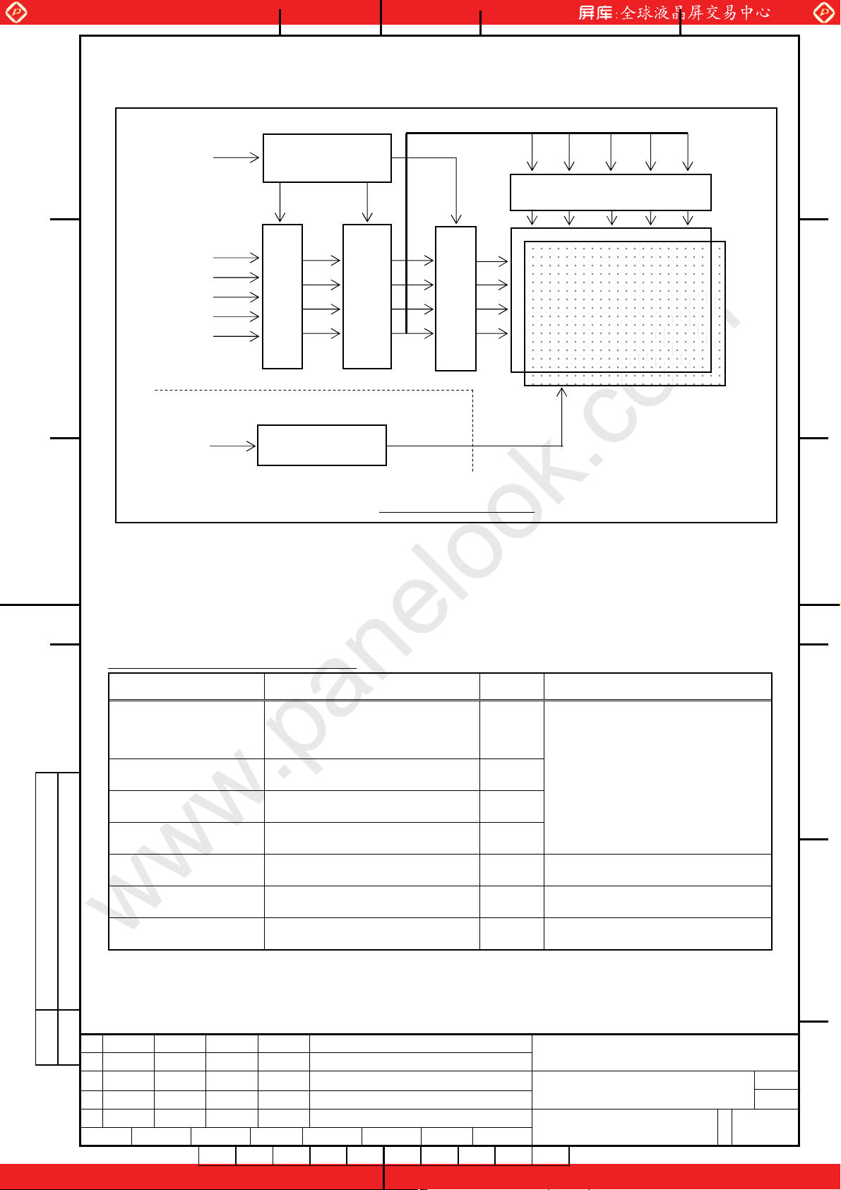
1. APPLICATION
2䋮 PRODUCT NAME AND MODEL NUMBER
LCD Module
3. OVERVIEW
4. CONFIGURATION
This specification is applied to the 15.0 in. XGA supported TFT-LCD module.
㪘㩷
2–1 Product Name :
2-2 Model Number
: NA19020-C262
㩷㩷㩷㩷㩷㩷㩷㩷㩷㩷㩷㩷㩷㩷㩷㩷㩷㩷㩷㩷㩷㩷
㪙㩷
This LCD module has a TFT active matrix type liquid crystal panel 1024×768 pixels, and
diagonal size of 38cm (15.0-inch). This module supports 1024×768 XGA mode (Non-interlace).
This LCD has a digital RGB interface and can display 262,144 colors.
Timing control signal is “Data enable signal : ENAB” only. (Data enable mode)
Even and odd data are transmitted at the same timing in the interface, so data lines are 36.
(R, G, B each 6 bit ×2) The signal level of this interface is +3.3V CMOS level or 5V TTL level.
The power supply of this LCD module is +5v DC single.
www.panelook.com
29
㪚㩷 㪚
This LCD module consists of a color TFT-LCD panel that is mounted with TFT driver ICs
䌡䌮䌤 a cold-cathode fluorescent tube back-light.
The inverter for the back-light is not included.
Figure 4-1 shows a block diagram of this LCD module.
㪛㩷
㪛
㪜
㪛㪘㪫㪜㩷 㪛㪦㪚㪬㪤㪜㪥㪫㩷㪚㪦㪥㪫㪩㪦㪣㩷㪪㪜㪚㪫㪠㪦㪥㩷
㪜㪛㪠㪫㩷
㪛㪜㪪㪠㪞㪅㩷
㪛㪘㪫㪜㩷
㪛㪜㪪㪠㪞㪅㩷 㪛㪜㪪㪚㪩㪠㪧㪫㪠㪦㪥
㪚㪟㪜㪚㪢
㪘㪧㪧㪩㪅㩷
㪚㪟㪜㪚㪢㩷
㪘㪧㪧㪩㪅
㪈㩷
One step solution for LCD / PDP / OLED panel application: Datasheet, inventory and accessory!
TITLE
NA19020-C262
DRAW. NO.
Tech Bes LCD-00067
FUJITSU DISPLAY TECHNOLOGIES
CORPORATION
㪚㪬㪪㪫㪅
䕣
䕘
3
䕕
㪆
䕕
䕤
www.panelook.com
Page 5
Global LCD Panel Exchange Center
5. MECHANICAL SPECIFICATIONS
V
V
㪘㩷
cc
(+5V)
DC/DC
Converter
www.panelook.com
Data Driver
㪙㩷
ENAB
RO-5
GO-5
BO-5
DCLK
LCD Panel
Interface Circuit
Control Circuit
Gate Driver
(External)
Backlight
DD
Inverter
㪚㩷 㪚
Fig.4-1.Block Diagram
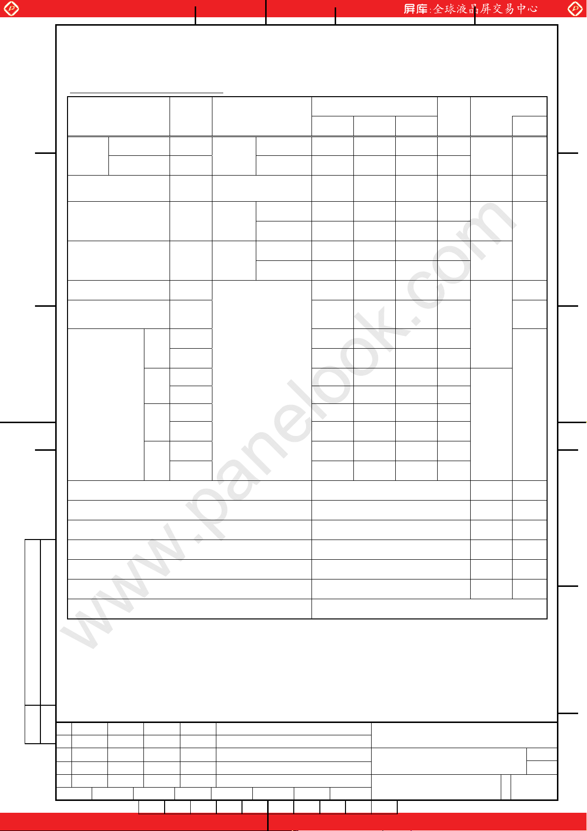
Table 5-1 shows the mechanical specifications of this LCD module.
Table 5-1. Mechanical Specifications
Item Specifications Unit Remark
㪛㩷
Dimensions
347.3×263.5×15.8(TYP.)
(Excluding I/F Connector
and fixing parts)
mm
Edge type backlight is used.
(φ2.6 CCFL×4)
㪛
Display Resolution (1024×3) ×768 —
Outward Appearance is shown
at page 31 and 32.
Display Dot Area 304.1×228.1 mm
Dot Pitch (0.099×3) ×0.297 mm
Aspect Ratio 1 : 1 —
Weight 1,400typ, 1,600max g
FG-SG Short circuit —
㪜
㪛㪘㪫㪜㩷 㪛㪦㪚㪬㪤㪜㪥㪫㩷㪚㪦㪥㪫㪩㪦㪣㩷㪪㪜㪚㪫㪠㪦㪥㩷
TITLE
NA19020-C262
DRAW. NO.
Tech Bes LCD-00067
㪚㪬㪪㪫㪅
㪜㪛㪠㪫㩷
㪛㪜㪪㪠㪞㪅㩷
㪛㪘㪫㪜㩷
㪛㪜㪪㪠㪞㪅㩷 㪛㪜㪪㪚㪩㪠㪧㪫㪠㪦㪥
㪚㪟㪜㪚㪢
㪘㪧㪧㪩㪅㩷
㪚㪟㪜㪚㪢㩷
㪘㪧㪧㪩㪅
FUJITSU DISPLAY TECHNOLOGIES
CORPORATION
㪈㩷
One step solution for LCD / PDP / OLED panel application: Datasheet, inventory and accessory!
䕣
䕘
4
䕕
㪆
䕕
䕤
www.panelook.com
Page 6
Global LCD Panel Exchange Center
6. ABSOLUTE MAXIMUM RATINGS
7. RECOMMENDED OPERATING CONDITIONS
Table 6-1 shows the absolute maximum rating of this LCD module.
㪘㩷
Table 6-1. Absolute Maximum Ratings
Item Symbol Condition MIN. TYP. MAX. Unit
www.panelook.com
Supply Voltage V
Input Voltage V
CC
IN
Ta=25ºC -0.3 — 6.0 V
Ta=25ºC -0.3 — Vcc+0.3 V
㪙㩷
Table 7-1 shows the recommended operating conditions of this LCD module.
Table 7-1. Recommended Operating Conditions
Item Symbol MIN. TYP. MAX. Unit
Supply Voltage (Logic) V
Ripple Voltage V
CC
CC
V
RP
㪚㩷 㪚
4.75 5.0 5.25 V
— — 100 mV
㪛㩷
㪛
㪜
TITLE
㪛㪘㪫㪜㩷 㪛㪦㪚㪬㪤㪜㪥㪫㩷㪚㪦㪥㪫㪩㪦㪣㩷㪪㪜㪚㪫㪠㪦㪥㩷
DRAW. NO.
NA19020-C262
Tech Bes LCD-00067
㪜㪛㪠㪫㩷
㪛㪜㪪㪠㪞㪅㩷
㪛㪘㪫㪜㩷
㪛㪜㪪㪠㪞㪅㩷 㪛㪜㪪㪚㪩㪠㪧㪫㪠㪦㪥
㪚㪟㪜㪚㪢
㪘㪧㪧㪩㪅㩷
㪚㪟㪜㪚㪢㩷
㪘㪧㪧㪩㪅
FUJITSU DISPLAY TECHNOLOGIES
CORPORATION
㪈㩷
One step solution for LCD / PDP / OLED panel application: Datasheet, inventory and accessory!
㪚㪬㪪㪫㪅
䕣
䕘
5
䕕
㪆
䕕
䕤
www.panelook.com
Page 7
Global LCD Panel Exchange Center
8. ELECTRICAL SPECIFICATIONS
Table 8-1 shows the electrical specifications of this LCD module.
㪘㩷
Table 8-1. Electrical Specifications
Item Symbol Condition MIN. TYP. MAX. Unit Remark
www.panelook.com
Supply Current I
CC
V
+5.0±0.25V
CC=
— 380 800 mA *1
Vss=0V
“H” Level Logic Input
Voltage
“L” Level Logic Input
Voltage
㪙㩷
Leak Current
(Logic Input)
Supply Rush Current I
Supply Rush Current
Duration (1A excess)
Contrast Regulation VR R
CCFL Turn on
㪚㩷 㪚
Voltage
Lighting Voltage
T
V
V
I
SCC
SCC
V
䌖
IL
VR
DCLK=32.505MHz
IH
IL
-5 — +5
2.3 — V
䌖
䌓䌓
— 0.9 V
CC
V
μA
— — 5.5 A *2
— — 0.4 ms
0 — 100
S
䌌
䌦䌌=50kHz,
Ta=25ºC
䌦䌌=50kHz,
Ta=0ºC
䌦䌌=50kHz
䌉
=7mA
䌌
— 1324 1500
Vrms
— 1324 1500
550 580 610 Vrms
kΩ
BACK LIGHT
Lighting Frequency
䌦
䌌
䌖䌌=580Vrms
40 50 60 kHz
*4
Tube Current
㩷
㪛㩷
(*1) Typical current value is measured when color bar pattern is displayed at Vcc=5.0V.
䌉
䌌
䌦䌌=50kHz
V
=580Vrms
䌌
6 7 8
Maximum current value is measured when 55/63 and 63/63 gray scale pattern every 2 pixel is
displayed at Vcc=4.75V.
Without rush current.
(*2) These items prescribe the rush current for starting internal DC/DC.
Charging current to capacitors of Vcc is not prescribed.
(*3) Backlight specifications are valid when using a suitable inverter such as the “FLCV-07” of
Fujitsu Limited.
(*4) Tube current (I
) shows the value of the current that is consumed at one lamp.
L
This LCD module has 4 lamps. Each 2 lamps are placed at upper and lower side of the
display.
2 lamps are connected in parallel. Each low voltage terminals are bound into 1 line cable,
which connected to the backlight connector.
㪛㪘㪫㪜㩷 㪛㪦㪚㪬㪤㪜㪥㪫㩷㪚㪦㪥㪫㪩㪦㪣㩷㪪㪜㪚㪫㪠㪦㪥㩷
㪜㪛㪠㪫㩷
㪛㪜㪪㪠㪞㪅㩷
㪛㪘㪫㪜㩷
㪛㪜㪪㪠㪞㪅㩷 㪛㪜㪪㪚㪩㪠㪧㪫㪠㪦㪥
㪚㪟㪜㪚㪢
㪘㪧㪧㪩㪅㩷
㪚㪟㪜㪚㪢㩷
㪘㪧㪧㪩㪅
TITLE
NA19020-C262
DRAW. NO.
Tech Bes LCD-00067
FUJITSU DISPLAY TECHNOLOGIES
CORPORATION
㪈㩷
One step solution for LCD / PDP / OLED panel application: Datasheet, inventory and accessory!
䌭A
*4
䕣
䕘
䕕
䕕
䕤
㪚㪬㪪㪫㪅
6
㪆
www.panelook.com
㪛
㪜
Page 8
Global LCD Panel Exchange Center
V
μ
μ
Note 1) Measurement Circuit
www.panelook.com
Based on Fig.8-1.
㪘㩷
㪙㩷
+5V
GND
AC
GND
C
Vs
Icc
Vcc
Logic Analog Driver
DC/DC
L
V
L
I
Converte
Backlight
LCD module
Fig.8-1. Measurement Circuit
Note 2) Equivalent Circuit
Based on Fig.8-2 (a), (b).
EMI Filter
㪚㩷 㪚
Input signals
㪛㩷
DCLK
ENAB
RO0~5,RE0~5
GO0~5,GE0~5
BO0~5,BE0~5
CMOS logic signal
(Internal)
EMI Filter ..........MEM2012TC100(TDK)
Fig.8-2 (a) Equivalent Circuit of Logic Signal Input
cc
GND
Fuse
(2A)
EMI Filter
10
Internal
Circuit
10
F
F
100pF
FG
䋨Frame ground䋩
Fuse.................. KAB2402202NA (Matsuo Electric CO., LTD.)
EMI Filter........ SGM20C1E332-2A (Sumitomo Metals)
Fig.8-2 (b) Equivalent Circuit of Power Supply
㪛
㪜
TITLE
㪛㪘㪫㪜㩷 㪛㪦㪚㪬㪤㪜㪥㪫㩷㪚㪦㪥㪫㪩㪦㪣㩷㪪㪜㪚㪫㪠㪦㪥㩷
DRAW. NO.
NA19020-C262
Tech Bes LCD-00067
㪜㪛㪠㪫㩷
㪛㪜㪪㪠㪞㪅㩷
㪛㪘㪫㪜㩷
㪛㪜㪪㪠㪞㪅㩷 㪛㪜㪪㪚㪩㪠㪧㪫㪠㪦㪥
㪚㪟㪜㪚㪢
㪘㪧㪧㪩㪅㩷
㪚㪟㪜㪚㪢㩷
㪘㪧㪧㪩㪅
FUJITSU DISPLAY TECHNOLOGIES
CORPORATION
㪈㩷
One step solution for LCD / PDP / OLED panel application: Datasheet, inventory and accessory!
㪚㪬㪪㪫㪅
䕣
䕘
7
䕕
㪆
䕕
䕤
www.panelook.com
Page 9
Global LCD Panel Exchange Center
9. OPTICAL SPECIFICATIONS
Table 9-1 shows the optical specifications of this LCD module.
Table 9-1. Optical Specifications
㪘㩷
Item Symbol Condition
www.panelook.com
Ta=25ºC,Signal timing=Typ
Specifications Remark
MIN. TYP. MAX.
Unit
Note
Visual
Angle
Horizontal
Verti cal
Contrast Ratio CR
Response
Time(ON)
㪙㩷
(B→W)
Response
Time(OFF)
(W→B)
Brightness I 200 250 — cd/m
Brightness
Uniformity
Chromaticity
W
θ
L,R
CR≥10
θ
t
t
U,D
ΔI
θ
L,R,U,D
θ
on
off
x 0.283 0.313 0.343 —
L,R,
=0º
U,D
θ
L,R,
=0º
U,D
θ
L,R,U,D
V
CC
=7mA
䌉
䌌
=50kHz
䌦
䌌
R*,G*,B* Signal
=All “H”
θ
=0º
U,D
θ
=0º
L,R
=0º
Ta=25ºC — 15 30 ms
Ta=0ºC — 50 100 ms
Ta=25ºC — 10 25 ms
Ta=0ºC — 50 100 ms
=0º
=5V,
y
80 — — deg
80 — — deg
210 400 — —
2
80 — — %
0.299 0.329 0.359 —
White/
Black
White
*1
㪚㩷 㪚
x
(0.643)
R
y
(0.353)
(1)(2)
(3)(5)
(6)
(1)(2)
(3)(5)
(1)
(4)
(5)
(1)(5)
(1)(5)
(7)
(1)
(5)
G
x
y
(0.285)
(0.600)
B
x
y
(0.145)
(0.126)
LCD Panel Type TFT Color
㪛㩷
Display Mode Normally Black VA
Wide Viewing Angle Technology MVA
Optimum Viewing Angle — (symmetry) (6)
Display Color 262,144 (6-bit color)
Color of non-display area Black
Surface Treatment
Anti-glare(Haze value :25%, 2H)
(*1) Value at 15~20 minutes after lighting on.
(Note) •CS-1000 (MINOLTA Co., Ltd.) , Field=1º, L=500mm
•Back-light current=7mA, Dark room condition(1lux or less)
•Be careful that the luminance meter, which tou use, may not be able to get correct brightness
If it’s set correctly.
㪛㪘㪫㪜㩷 㪛㪦㪚㪬㪤㪜㪥㪫㩷㪚㪦㪥㪫㪩㪦㪣㩷㪪㪜㪚㪫㪠㪦㪥㩷
TITLE
NA19020-C262
DRAW. NO.
Tech Bes LCD-00067
㪛
㪜
㪚㪬㪪㪫㪅
㪜㪛㪠㪫㩷
㪛㪜㪪㪠㪞㪅㩷
㪛㪘㪫㪜㩷
㪛㪜㪪㪠㪞㪅㩷 㪛㪜㪪㪚㪩㪠㪧㪫㪠㪦㪥
㪚㪟㪜㪚㪢
㪘㪧㪧㪩㪅㩷
㪚㪟㪜㪚㪢㩷
㪘㪧㪧㪩㪅
FUJITSU DISPLAY TECHNOLOGIES
CORPORATION
㪈㩷
One step solution for LCD / PDP / OLED panel application: Datasheet, inventory and accessory!
䕣
䕘
8
䕕
㪆
䕕
䕤
www.panelook.com
Page 10
Global LCD Panel Exchange Center
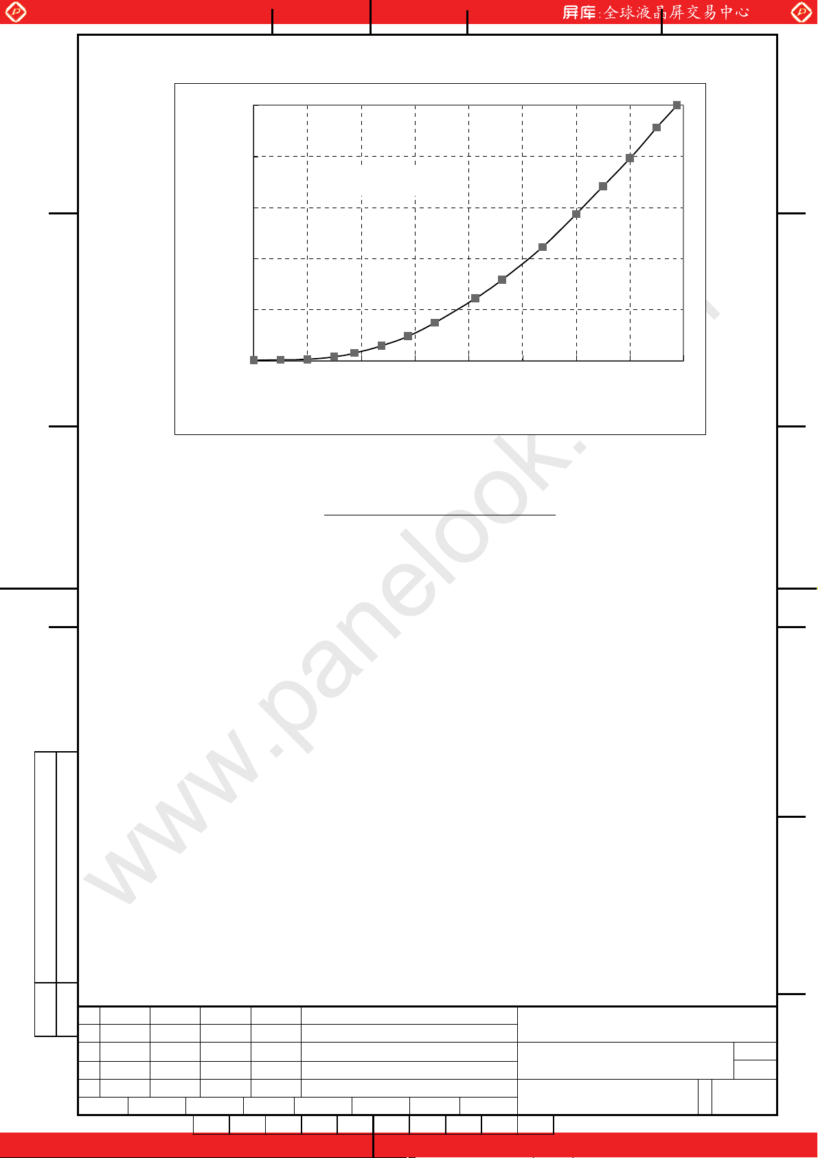
㪈㪇㪇
㪘㩷
㪏㪇
㪍㪇
㪋㪇
Brightness Ratio [%]
㪙㩷
㪉㪇
㪇
0 8 16 24 32 40 48 56 64
www.panelook.com
γ =2.40(TYP.)
Gray Scale Level
㪚㩷 㪚
Fig.9-1. γ -Curve (Reference Value)
㪛㩷
㪛
TITLE
㪛㪘㪫㪜㩷 㪛㪦㪚㪬㪤㪜㪥㪫㩷㪚㪦㪥㪫㪩㪦㪣㩷㪪㪜㪚㪫㪠㪦㪥㩷
㪜㪛㪠㪫㩷
㪛㪜㪪㪠㪞㪅㩷
㪛㪘㪫㪜㩷
㪛㪜㪪㪠㪞㪅㩷 㪛㪜㪪㪚㪩㪠㪧㪫㪠㪦㪥
㪚㪟㪜㪚㪢
㪘㪧㪧㪩㪅㩷
㪚㪟㪜㪚㪢㩷
㪘㪧㪧㪩㪅
NA19020-C262
DRAW. NO.
Tech Bes LCD-00067
FUJITSU DISPLAY TECHNOLOGIES
CORPORATION
㪈㩷
One step solution for LCD / PDP / OLED panel application: Datasheet, inventory and accessory!
㪜
㪚㪬㪪㪫㪅
䕣
䕘
9
䕕
㪆
䕕
䕤
www.panelook.com
Page 11

Global LCD Panel Exchange Center
)
www.panelook.com
Note 1) Definition of Viewing Angle (1)
㪘㩷
Based on Fig.9-2.
㩷 Y
Top (12 o’clock Direction)
+
θ
L
θ
U
*0º (Front
θ
R
θ
D
㩷㩷 X
+
Right (3 o’clock Direction)
LCD module
㪙㩷
㩷㩷㩷㩷㩷㩷㩷㩷㩷㩷X
Left (9 o’clock Direction)
−
* → θ
=0º,θD=0º,θL=0º,θR=0º
U
㩷㩷㩷㩷㩷㩷㩷㩷㩷㩷Y
Bottom (6 o’clock Direction)
−
Fig.9-2. Definition of Viewing Angle (1)
Note 2) Definition of Viewing Angle (2)
㪚㩷 㪚
Based on Fig.9-3.
Display Surface
θ
L,R,U,D
=0º
θ
θ
MIN
θ
TYP
MAX
Display Surface
㪛㩷
Fig.9-3. Definition of Viewing Angle (2)
Note 3) Definition of Contrast Ratio (CR)
Determined by Formula (1) based on
L
W
Fig.9-4.Voltage-Brightness
Characteristics.
L
(Brightness at white)
W
= -------- (1)
L
(Brightness at black)
B
Brightness
[L]
L
0
Black
B
0
Panel Drive Voltage [V]
Fig.9-4. Voltage-Brightness Characteristics
TITLE
㪛㪘㪫㪜㩷 㪛㪦㪚㪬㪤㪜㪥㪫㩷㪚㪦㪥㪫㪩㪦㪣㩷㪪㪜㪚㪫㪠㪦㪥㩷
㪜㪛㪠㪫㩷
㪛㪜㪪㪠㪞㪅㩷
㪛㪘㪫㪜㩷
㪛㪜㪪㪠㪞㪅㩷 㪛㪜㪪㪚㪩㪠㪧㪫㪠㪦㪥
㪚㪟㪜㪚㪢
㪘㪧㪧㪩㪅㩷
㪚㪟㪜㪚㪢㩷
㪘㪧㪧㪩㪅
NA19020-C262
DRAW. NO.
Tech Bes LCD-00067
FUJITSU DISPLAY TECHNOLOGIES
CORPORATION
㪈㩷
One step solution for LCD / PDP / OLED panel application: Datasheet, inventory and accessory!
㪛
White
㪜
㪚㪬㪪㪫㪅
䕣
䕘
10
䕕
㪆
䕕
䕤
www.panelook.com
Page 12

Global LCD Panel Exchange Center
www.panelook.com
Note 4) Definition of Response Time
Based on Fig.9-5.
㪘㩷
Drive signal
of LCD panel
㪙㩷
Relative
Brightness
㪚㩷 㪚
Note 5) Contrast Ratio and Response Measurement System
ON
OFF
Non-select status
100%
0%
Select status
90%
White
Black
t
on
ON Response Time
Fig.9-5. Definition of Response Time
Non-select status
10%
t
off
OFF Response Time
Black
㪛㩷
Based on Fig.9-6.
+
Y
+
X
−
Z
−
X
−
Y
+
Z
Brightness Meter or
θ
Luminance Colorimeter
㪛
(with luminosity
correction function)
Drive and Measurement System
㪜
Fig.9-6. Contrast Ratio and Response Time Measurement System
TITLE
㪛㪘㪫㪜㩷 㪛㪦㪚㪬㪤㪜㪥㪫㩷㪚㪦㪥㪫㪩㪦㪣㩷㪪㪜㪚㪫㪠㪦㪥㩷
㪜㪛㪠㪫㩷
㪛㪜㪪㪠㪞㪅㩷
㪛㪘㪫㪜㩷
㪛㪜㪪㪠㪞㪅㩷 㪛㪜㪪㪚㪩㪠㪧㪫㪠㪦㪥
㪚㪟㪜㪚㪢
㪘㪧㪧㪩㪅㩷
㪚㪟㪜㪚㪢㩷
㪘㪧㪧㪩㪅
NA19020-C262
DRAW. NO.
Tech Bes LCD-00067
FUJITSU DISPLAY TECHNOLOGIES
CORPORATION
㪈㩷
One step solution for LCD / PDP / OLED panel application: Datasheet, inventory and accessory!
㪚㪬㪪㪫㪅
䕣
䕘
11
䕕
㪆
䕕
䕤
www.panelook.com
Page 13

Global LCD Panel Exchange Center
Note 6) Definition of Optimum Viewing Angle
Based on Fig.9-7.
㪘㩷
www.panelook.com
㩷 MAX
Contrast
Ratio
㪙㩷
10
(-)
6 o’clock ← Viewing Angle → 12 o’clock
Fig.9-7. Definition of Viewing Angle
Note 7) Definition of Brightness Uniformity
Brightness uniformity is defined by the following formula.
㪚㩷 㪚
Brightness (I1~I9) art measured at the following 9 points ( 1 ~ 9 ) on the display
area shown in Fig.9-8.
|Min. In|
Brightness Uniformity (ΔL) = × 100 (%), n=1 to 9
|Max. In|
(+)0
153 512 871
㪛㩷
1 4 7
115
2 5 8
384
3 6 9
653
Note) Each measurement point ( 1 ~ 9 ) defines the center spot of Brightness Meter view.
The tolerance of measurement position is ±5mm.
Fig.9-8. Measurement Points
TITLE
㪛㪘㪫㪜㩷 㪛㪦㪚㪬㪤㪜㪥㪫㩷㪚㪦㪥㪫㪩㪦㪣㩷㪪㪜㪚㪫㪠㪦㪥㩷
㪜㪛㪠㪫㩷
㪛㪜㪪㪠㪞㪅㩷
㪛㪘㪫㪜㩷
㪛㪜㪪㪠㪞㪅㩷 㪛㪜㪪㪚㪩㪠㪧㪫㪠㪦㪥
㪚㪟㪜㪚㪢
㪘㪧㪧㪩㪅㩷
㪚㪟㪜㪚㪢㩷
㪘㪧㪧㪩㪅
NA19020-C262
DRAW. NO.
Tech Bes LCD-00067
FUJITSU DISPLAY TECHNOLOGIES
CORPORATION
㪈㩷
One step solution for LCD / PDP / OLED panel application: Datasheet, inventory and accessory!
㪛
㪜
㪚㪬㪪㪫㪅
䕣
䕘
12
䕕
㪆
䕕
䕤
www.panelook.com
Page 14
Global LCD Panel Exchange Center
10. INTERFACE SPECIFICATIONS
—
—
—
—
—
—
—
K
g
—
—
—
—
—
—
—
—
—
VDD—
VDD—
—
VDD—
VDD—
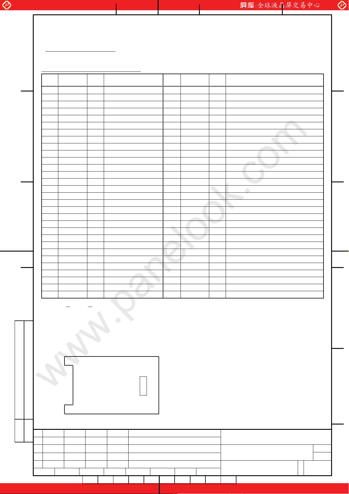
10-1. Signal descriptions
www.panelook.com
㪘㩷
Table 10-1. Interface signals (CN1)
㪙㩷
㪚㩷 㪚
㪛㩷
Table 10-1 shows the description and configuration of Interface signals (CN1).
Pin
Symbol I/O Function
㷗
1 GND
2 RE0
3 RE1
4 RE2
5 RE3
6 RE4
7 RE5
8 GND
9 GE0
10 GE1
11 GE2
12 GE3
13 GE4
14 GE5
15 GND
16 BE0
17 BE1
18 BE2
19 BE3
20 BE4
21 BE5
22 GND
23 RO0
24 RO1
25 RO2
26 RO3
27 RO4
28 RO5
29 GND
30 GO0
Ground 31 GO1
Red even data 0 32 GO2
䌉
Red even data 1 33 GO3
䌉
Red even data 2 34 GO4
䌉
Red even data 3 35 GO5
䌉
Red even data 4 36 GND
䌉
Red even data 5 37 BO0
䌉
Ground 38 BO1
Green even data 0 39 BO2
䌉
Green even data 1 40 BO3
䌉
Green even data 2 41 BO4
䌉
Green even data 3 42 BO5
䌉
Green even data 4 43 GND
䌉
Green even data 5 44 PULL
䌉
Ground 45 PULL
Blue even data 0 46 ENAB
䌉
Blue even data 1 47 GND
䌉
Blue even data 2 48 GND
䌉
Blue even data 3 49 DCL
䌉
Blue even data 4 50 GND
䌉
Blue even data 5 51 GND
䌉
Ground 52 SS
Red odd data 0 53 N.C.
䌉
Red odd data 1 54 GND
䌉
Red odd data 2 55 GND
䌉
Red odd data 3 56 GND
䌉
Red odd data 4 57
䌉
Red odd data 5 58
䌉
Ground 59
Green odd data 0 60
䌉
Pin
Symbol I/O Function
㷗
Green odd data 1
䌉
Green odd data 2
䌉
Green odd data 3
䌉
Green odd data 4
䌉
Green odd data 5
䌉
Ground
Blue odd data 0
䌉
Blue odd data 1
䌉
Blue odd data 2
䌉
Blue odd data 3
䌉
Blue odd data 4
䌉
Blue odd data 5
䌉
Ground
(*2)
䌉
(*2)
䌉
Data enable signal
䌉
Ground
Ground
Dot clock si
䌉
Ground
Ground
SS function ON/OFF (*1)
Ground
Ground
Ground
+5V Power supply
+5V Power supply
+5V Power supply
+5V Power supply
nal
(*1) SS (Spread Spectrum):SS function is ON when signal level is high or N.C..(generally set up N.C.)
SS function is OFF when signal level is low.
㪛
(*2).Connect it to GND for the protection of internal circuit.
Upper side
㩷 Interface connector
LCD Module
Rear side
31 30
60 1
Connector : 52760-0600 (Molex)
User’s connector : 53475-0600 (Molex)
Lower side
㪛㪘㪫㪜㩷 㪛㪦㪚㪬㪤㪜㪥㪫㩷㪚㪦㪥㪫㪩㪦㪣㩷㪪㪜㪚㪫㪠㪦㪥㩷
㪜㪛㪠㪫㩷
㪛㪜㪪㪠㪞㪅㩷
㪛㪘㪫㪜㩷
㪛㪜㪪㪠㪞㪅㩷 㪛㪜㪪㪚㪩㪠㪧㪫㪠㪦㪥
㪚㪟㪜㪚㪢
㪘㪧㪧㪩㪅㩷
㪚㪟㪜㪚㪢㩷
㪘㪧㪧㪩㪅
TITLE
NA19020-C262
DRAW. NO.
Tech Bes LCD-00067
FUJITSU DISPLAY TECHNOLOGIES
CORPORATION
㪈㩷
One step solution for LCD / PDP / OLED panel application: Datasheet, inventory and accessory!
䕣
䕘
䕕
䕕
䕤
www.panelook.com
13
㪜
㪚㪬㪪㪫㪅
㪆
Page 15

Global LCD Panel Exchange Center
www.panelook.com
10-2. Color Data Assignment
Table 10-2 shows the color data assignment.
㪘㩷
Table 10-2. Color Data Assignment
Color R Input data G Input data B Input data
Odd
Even
R05 R04 R03 R02 R01 R00 G05 G04 G03 G02 G01 R00 B05 B04 B03 B02 B01 B00
RE5 RE4 RE3 RE2 RE1 RE0 GE5 GE4 GE3 GE2 GE1 GE0 BE5 BE4 BE3 BE2 BE1 BE0
Black 0 0 0 0 0 0 0 0 0 0 0 0 0 0 0 0 0 0
Blue 0 0 0 0 0 0 0 0 0 0 0 0 1 1 1 1 1 1
Green 0 0 0 0 0 0 1 1 1 1 1 1 0 0 0 0 0 0
Cyan 0 0 0 0 0 0 1 1 1 1 1 1 1 1 1 1 1 1
㪙㩷
Red 1 1 1 1 1 1 0 0 0 0 0 0 0 0 0 0 0 0
Magenta 1 1 1 1 1 1 0 0 0 0 0 0 1 1 1 1 1 1
Basic Color
Yellow 1 1 1 1 1 1 1 1 1 1 1 1 1 1 1 1 1 1
White 1 1 1 1 1 1 1 1 1 1 1 1 0 0 0 0 0 0
Black
×
×
Red
Ø
Brighter
Ø
㪚㩷 㪚
Red
Black
×
×
Ø
Green
Brighter
Ø
Green
Black
㪛㩷
×
×
Ø
Blue
Brighter
Ø
Blue
0
0 0 0 0 0 0 0 0 0 0 0 0 0 0 0 0 0 0
1
0 0 0 0 0 1 0 0 0 0 0 0 0 0 0 0 0 0
61
1 1 1 1 0 1 0 0 0 0 0 0 0 0 0 0 0 0
62
1 1 1 1 1 0 0 0 0 0 0 0 0 0 0 0 0 0
63
1 1 1 1 1 1 0 0 0 0 0 0 0 0 0 0 0 0
0
0 0 0 0 0 0 0 0 0 0 0 0 0 0 0 0 0 0
1
0 0 0 0 0 0 0 0 0 0 0 1 0 0 0 0 0 0
61
0 0 0 0 0 0 1 1 1 1 0 1 0 0 0 0 0 0
62
0 0 0 0 0 0 1 1 1 1 1 0 0 0 0 0 0 0
63
0 0 0 0 0 0 1 1 1 1 1 1 0 0 0 0 0 0
0
0 0 0 0 0 0 0 0 0 0 0 0 0 0 0 0 0 0
1
0 0 0 0 0 0 0 0 0 0 0 0 0 0 0 0 0 1
61
0 0 0 0 0 0 0 0 0 0 0 0 1 1 1 1 0 1
62
0 0 0 0 0 0 0 0 0 0 0 0 1 1 1 1 1 0
63
0 0 0 0 0 0 0 0 0 0 0 0 1 1 1 1 1 1
Note.1) Definition of gray scale : Color (n) ---”n” indicates gray scale level.
The gray scale is brighter as the number is larger.
Note.2) Data; 1: High, 0: Low
Note.3) Color data consist of 36 bits, namely, 6-bit odd and even data for each red, green and blue.
Optional data can be set to red, green and blue independently.
Therefore, the module is able to display 262,144 colors.
㪛
㪜
㪛㪘㪫㪜㩷 㪛㪦㪚㪬㪤㪜㪥㪫㩷㪚㪦㪥㪫㪩㪦㪣㩷㪪㪜㪚㪫㪠㪦㪥㩷
㪜㪛㪠㪫㩷
㪛㪜㪪㪠㪞㪅㩷
㪛㪘㪫㪜㩷
㪛㪜㪪㪠㪞㪅㩷 㪛㪜㪪㪚㪩㪠㪧㪫㪠㪦㪥
㪚㪟㪜㪚㪢
㪘㪧㪧㪩㪅㩷
㪚㪟㪜㪚㪢㩷
㪘㪧㪧㪩㪅
TITLE
NA19020-C262
DRAW. NO.
Tech Bes LCD-00067
FUJITSU DISPLAY TECHNOLOGIES
CORPORATION
㪈㩷
One step solution for LCD / PDP / OLED panel application: Datasheet, inventory and accessory!
㪚㪬㪪㪫㪅
䕣
䕘
䕕
14
㪆
䕕
䕤
www.panelook.com
Page 16

Global LCD Panel Exchange Center
www.panelook.com
10-3. Input Signal Timing
Table 10-3 and Fig.10-3 shows the input signal timing.
Table 10-3. Timing Characteristics
㪘㩷
(T=0~50ºC, Vcc=5±0.25V)
Item Symbol Min. Typ. Max. Unit Remark
DCLK signal Period Tc 25.000 30.764 40.000 ns
(Clock) Frequency fc 25.000 32.505 40.000 MHz fc=1/Tc
Duty Tch/Tc 45 50 55 䋦 *1
High time TclkH 5.0 — — ns
Low time TclkL 5.0 — — ns
Rise time Tclkr — — 5.0 ns
Fall time Tclkf — — 5.0 ns
㪙㩷
DCLK-Data Setup time Tset 4.5 — — ns 40MHz
Timing Hold time Thold 6.5 — — ns 40MHz
Horizontal Period Th 565 672 1566 DCLK fh=1/Th
Frequency fh 38.6 48 60 kHz
Display period Thd — 512 — DCLK *2,3
Ver ti ca l Period Tv 772 806 868 Th 16.67ms
Frequency fv 50 60 75 Hz
Display period Tvd — 768 — Th *2,3
Data-ENAB timing
Data-ENAB timing — — 0 — DCLK *4
*1) DCLK signal input must be valid while power supply is applied.
㪚㩷 㪚
*2) Display position is specified by the ENAB signal.
䊶Horizontal display position is specified by the rise of ENAB signal. The data of a horizontal
line, which is latched by the falling edge of 1st DCLK right after the rise of ENAB, is
displayed on the left edge of the screen.
䊶Vertical display position is specified by the rise of ENAB after a “Low” level period
equivalent to eight times of horizontal period. The 1st data corresponding to one horizontal
line after the rise of ENAB is displayed at the top line of screen.
*3) If a period of ENAB “High” is less than 512 DCLK or less than 768 lines, the rest of the screen
㪛㩷
displays black.
*4) The display position does not fit to the screen if the ENAB period and the effective data period
do not synchronize with each other.
㪛
㪛㪘㪫㪜㩷 㪛㪦㪚㪬㪤㪜㪥㪫㩷㪚㪦㪥㪫㪩㪦㪣㩷㪪㪜㪚㪫㪠㪦㪥㩷
㪜㪛㪠㪫㩷
㪛㪜㪪㪠㪞㪅㩷
㪛㪘㪫㪜㩷
㪛㪜㪪㪠㪞㪅㩷 㪛㪜㪪㪚㪩㪠㪧㪫㪠㪦㪥
㪚㪟㪜㪚㪢
㪘㪧㪧㪩㪅㩷
㪚㪟㪜㪚㪢㩷
㪘㪧㪧㪩㪅
TITLE
NA19020-C262
DRAW. NO.
Tech Bes LCD-00067
FUJITSU DISPLAY TECHNOLOGIES
CORPORATION
㪈㩷
One step solution for LCD / PDP / OLED panel application: Datasheet, inventory and accessory!
㪜
㪚㪬㪪㪫㪅
䕣
䕘
䕕
15
㪆
䕕
䕤
www.panelook.com
Page 17

Global LCD Panel Exchange Center
v
www.panelook.com
㩷
㪘㩷
DCLK
ENAB
RO5-5, RE5-0
GO5-0, GE5-0
TclkL
Tclkr Tclkf
0.9V
Tc1
Tc
Tclk
2.3V
Tch
1.65V
Tset
Thol
2.3V
0.9V
BO5-0, BE5-0
㪙㩷
RO5-0, RE5-0
GO5-0, GE5-0
BO5-0, BE5-0
ENAB
Th
㪚㩷 㪚
Th
RO5-0, RE5-0
C001 C768
GO5-0, GE5-0
BO5-0, BE5-0
ENAB
T
㪛㩷
Tc
Tv
DCLK
RO5-0, RE5-0
GO5-0, GE5-0
0001
0003
0005
0007
0009
0011
1011
1013
1017 1021
1015
1019
1023
BO5-0, BE5-0
0002
0004
0006
0008
0010
0012
1012
1014
1016
1018
1020
1022
1024
ENAB
Tdn=0clk
Tdn=0clk
Fig.10-3.Input Signal Timing Chart
㪛
㪜
㪛㪘㪫㪜㩷 㪛㪦㪚㪬㪤㪜㪥㪫㩷㪚㪦㪥㪫㪩㪦㪣㩷㪪㪜㪚㪫㪠㪦㪥㩷
㪜㪛㪠㪫㩷
㪛㪜㪪㪠㪞㪅㩷
㪛㪘㪫㪜㩷
㪛㪜㪪㪠㪞㪅㩷 㪛㪜㪪㪚㪩㪠㪧㪫㪠㪦㪥
㪚㪟㪜㪚㪢
㪘㪧㪧㪩㪅㩷
㪚㪟㪜㪚㪢㩷
㪘㪧㪧㪩㪅
TITLE
NA19020-C262
DRAW. NO.
Tech Bes LCD-00067
FUJITSU DISPLAY TECHNOLOGIES
CORPORATION
㪈㩷
One step solution for LCD / PDP / OLED panel application: Datasheet, inventory and accessory!
㪚㪬㪪㪫㪅
䕣
䕘
䕕
16
㪆
䕕
䕤
www.panelook.com
Page 18

Global LCD Panel Exchange Center
V
www.panelook.com
.
㪘㩷
10-4. Correspondence between Data and Display Position
Fig.10-3 shows the Correspondence between Data and Display Position
C001
S0001 S0002 S0003 S0004 S0005 S0006 S0007
㩷㩷㩷㩷㩷㩷㩷㩷 㩷 㩷㩷㩷
RO
0001
GO
0001
BO
0001
RE
0002
GE
0002
BE
0002
RO
0003
GO
0003
S3071 S3072
GE
1024
BE
1024
㪙㩷
GE
1024
BE
1024
C768
RO
0001
GO
0001
BO
0001
RE
0002
GE
0002
BE
0002
RO
0003
GO
0003
Fig.10-4.Correspondence Data and Display Position
㪚㩷 㪚
10-5. Power Supply Sequence
The sequence of input signals and On/Off of the power supply of this LCD module should be
in the specification shown in Fig.10-4 to prevent latch-up of the driver ICs and DC driving
of the LCD panel.
㪛㩷
㩷
㩷
㩷
㩷
cc
㩷
ON
OFF
(0V)
4.75V
T4<
20ms
㩷
T5<20ms(Voltage descent)
亖
亖
4.75V
(4.5V)
4.75V
0.5V
0.5<
4.75V
T6
㩷
亖
㩷
㩷
Input signal
㩷
㩷
㩷
㩷
㩷
H
L
T1
T2
90%
10%
10ms<
10ms<
T1<40ms
T2<40ms
亖
10%
0ms<
T3<40ms
㩷
㩷
Fig.10-5. Power Supply Sequence
㪛
㪜
Note)If power Supply Sequence not followed, the CMOS-IC may cause a latch-up, or DC voltage
May be applied to the liquid crystal, which cause a failure or serious deterioration in display
quality.
㪛㪘㪫㪜㩷 㪛㪦㪚㪬㪤㪜㪥㪫㩷㪚㪦㪥㪫㪩㪦㪣㩷㪪㪜㪚㪫㪠㪦㪥㩷
㪜㪛㪠㪫㩷
㪛㪜㪪㪠㪞㪅㩷
㪛㪘㪫㪜㩷
㪛㪜㪪㪠㪞㪅㩷 㪛㪜㪪㪚㪩㪠㪧㪫㪠㪦㪥
㪚㪟㪜㪚㪢
㪘㪧㪧㪩㪅㩷
㪚㪟㪜㪚㪢㩷
㪘㪧㪧㪩㪅
TITLE
NA19020-C262
DRAW. NO.
Tech Bes LCD-00067
FUJITSU DISPLAY TECHNOLOGIES
CORPORATION
㪈㩷
One step solution for LCD / PDP / OLED panel application: Datasheet, inventory and accessory!
䕣
䕘
䕕
䕕
䕤
www.panelook.com
17
㪚㪬㪪㪫㪅
㪆
Page 19

Global LCD Panel Exchange Center
11. BACKLIGHT SPECIFICATIONS
11-1. Pin Configuration for Backlight
㪘㩷
㩷
Table 11-1(a) Pin Assignment of CN-A
Table 11-1(a) and 11-1(b) shows the description and pin assignment of the connectors (CN-A
and B) for the Backlight of this LCD module.
Pin
Signal Function
№
1 VL1 Power supply for CCFL 1 1 VL3 Power supply for CCFL 3
2 VL2 Power supply for CCFL 2 2 VL4 Power supply for CCFL 4
www.panelook.com
Table11-1(b) Pin Assignment of CN-B
Pin
Signal Function
№
3 NC
――
3 NC
――
㪙㩷
4 GND Ground (for VL1, 2) 4 GND Ground (for VL3, 4)
Cable color (CN-A and B) : White at GND, Pink at V
1,2,3 and 4
L
Connector : Housing : BHR-04VS-1
: Contact : SBH-001T-P0.5
User’s Connector : Post with base : SM04(4.0)B-BHS-1-TB
Supplier : Japan Solderless Terminal Trading Company LTD. (J.S.T.)
㪚㩷 㪚
11-2. CCFL
Supplier : SANKEN ELECTRIC CO., LTD Part No. KFN8319F315296Z
11-3. Life
The life of the backlight is a minimum of 50,000 hours at the following conditions.
(1) Working conditions
㪛㩷
① Ambient temperature : 25
② Tube current(I
) : (7mA or less)
L
㫧5ºC
(2) Definition of life
① Brightness becomes 50% or below 50% of the minimum brightness value shown in Table
9-1.
② The lamp cannot be lit by the breakdown voltage of 1500Vvms.
③ Lamp is flashing.
㪛
11-4. Lamp Assembly set (for replacement)
Lamp Assembly set (with charge) is prepared for maintenance.
This set consists of an upper lamp assembly and a lower lamp assembly.
Type number : FLCL-16S (for upper and lower)
㪛㪘㪫㪜㩷 㪛㪦㪚㪬㪤㪜㪥㪫㩷㪚㪦㪥㪫㪩㪦㪣㩷㪪㪜㪚㪫㪠㪦㪥㩷
㪜㪛㪠㪫㩷
㪛㪜㪪㪠㪞㪅㩷
㪛㪘㪫㪜㩷
㪛㪜㪪㪠㪞㪅㩷 㪛㪜㪪㪚㪩㪠㪧㪫㪠㪦㪥
㪚㪟㪜㪚㪢
㪘㪧㪧㪩㪅㩷
㪚㪟㪜㪚㪢㩷
㪘㪧㪧㪩㪅
TITLE
NA19020-C262
DRAW. NO.
Tech Bes LCD-00067
FUJITSU DISPLAY TECHNOLOGIES
CORPORATION
㪈㩷
One step solution for LCD / PDP / OLED panel application: Datasheet, inventory and accessory!
㪜
㪚㪬㪪㪫㪅
䕣
䕘
䕕
18
㪆
䕕
䕤
www.panelook.com
Page 20

Global LCD Panel Exchange Center
12. APPEARANCE SPECIFICATIONS
12-1 Appearance
㪘㩷
No. Item Judgment method and standard
1 Bright spot (high and Low) < 8 dots (Note 1 )
2 Bright spot connection
3 Total of bright spot < 8 dots
4 Dark spot < 18 dots (Note 2)
5 Dark spot connection
㪙㩷
6 Total of dark spot < 10 dots (Note 2)
7 Total of dot defect
8 Distance of dot defect > 2mm
(high and low)
www.panelook.com
2 dots connection < 2 pair (Note 1)
3 dots connection <
2 dots connection <
3 dots connection <
<
18 dots
1 pair
3 pair (Note 2)
1 pair
Ignore
9 Black / white spot
D < 0.3
0.3 < D < 0.6 N < 5
0.6 < D < 0.9 N < 2(Distance >100mm)
0.9 < D 0
10 Mura Ignore
㪚㩷 㪚
D:Average diameter [mm], W:Width [mm], L:Length [mm], S=(bright spot size)/(dot size)
㪛㩷
㪛
㪛㪘㪫㪜㩷 㪛㪦㪚㪬㪤㪜㪥㪫㩷㪚㪦㪥㪫㪩㪦㪣㩷㪪㪜㪚㪫㪠㪦㪥㩷
㪜㪛㪠㪫㩷
㪛㪜㪪㪠㪞㪅㩷
㪛㪘㪫㪜㩷
㪛㪜㪪㪠㪞㪅㩷 㪛㪜㪪㪚㪩㪠㪧㪫㪠㪦㪥
㪚㪟㪜㪚㪢
㪈㩷
One step solution for LCD / PDP / OLED panel application: Datasheet, inventory and accessory!
㪘㪧㪧㪩㪅㩷
㪚㪟㪜㪚㪢㩷
㪘㪧㪧㪩㪅
TITLE
NA19020-C262
DRAW. NO.
Tech Bes LCD-00067
FUJITSU DISPLAY TECHNOLOGIES
CORPORATION
㪜
㪚㪬㪪㪫㪅
䕣
䕘
䕕
19
㪆
䕕
䕤
www.panelook.com
Page 21

Global LCD Panel Exchange Center
www.panelook.com
12-2 Dot defects (Bright spots, Dark spots)
㪘㩷
12-2-1 Zone
· Inside display dot area (304.1×228.1mm)
· Display dot area means active area.
· One pixel consists of 3 dots (red, green and blue).
· Foreign particle and scratch unharmful to display image, such as the foreign particle
under polarizer film but outside of the display area and scratch on metal bezel, backlight
module or polarizer film out of the display area, etc., are not counted.
㪙㩷
12-2-2 Bright spots
(1) Bright spots by the defect of TFT.
· Visible under bias of 2% ND filter................................... High bright spot R•G
· Visible under 5% but invisible under 2% ND filter........ Low bright spot R•G•B
· Invisible under bias of 5% ND filter................................ Not counted
(2) Bright spots by the light passing through tears, breaks, etc in color filter.
· Exceed size of a half dot ................................................... High bright spot
· A half dot or less................................................................ Not counted
(3) Bright spots by the light passing through tears, breaks, etc in chromium mask.
㪚㩷 㪚
· Exceed 50μm ..................................................................... High bright spot
· 50μm or less ..................................................................... Not counted
㪛㩷
12-2-3 Test condition
· Inspector must observe the LCD screen from the normal direction under the illumination by
a single 20W fluorescent lamp. The distance between the LCD screen and the inspector
should be a height of 50cm above the worktable.
The vertical illuminance is 300 to 600lux (reference value).
· Bright spot should be counted under entire black screen.
· Dark spot should be counted under entire white screen.
· Input signal timing should be typical value.
(Note1) Please do not mistake a single bright spot for a bright spot connection due to
Cs(supplemental capacitance) line at the center of each dot.
(Note2) If a pixel is dark partially, it connects into the number of dark spots in accordance with
following rule.
(a) A<1/3 : Not count. Only one of 4 dark connection is allowed.
(b) 1/3<
(c) 2/3<
A<2/3 : Considered as 0.5 dot.
A : Considered as 1 dot.
(A=Dark spot size/dot size)㩷
㪛
㪜
㪛㪘㪫㪜㩷 㪛㪦㪚㪬㪤㪜㪥㪫㩷㪚㪦㪥㪫㪩㪦㪣㩷㪪㪜㪚㪫㪠㪦㪥㩷
㪜㪛㪠㪫㩷
㪛㪜㪪㪠㪞㪅㩷
㪛㪘㪫㪜㩷
㪛㪜㪪㪠㪞㪅㩷 㪛㪜㪪㪚㪩㪠㪧㪫㪠㪦㪥
㪚㪟㪜㪚㪢
㪈㩷
One step solution for LCD / PDP / OLED panel application: Datasheet, inventory and accessory!
㪘㪧㪧㪩㪅㩷
㪚㪟㪜㪚㪢㩷
㪘㪧㪧㪩㪅
TITLE
NA19020-C262
DRAW. NO.
Tech Bes LCD-00067
FUJITSU DISPLAY TECHNOLOGIES
CORPORATION
㪚㪬㪪㪫㪅
䕣
䕘
䕕
20
㪆
䕕
䕤
www.panelook.com
Page 22

Global LCD Panel Exchange Center
13. ENVIRONMENTAL SPECIFICATIONS
(
www.panelook.com
㪘㩷
Table 13-1 shows the environmental specifications.
Table 13-1. Environmental Specifications
Item Condition Remark
Temperature on surface of
LCD panel (display area.)
Maximum wet-bulb temperature
should not exceed 29º
C.
No condensation.
For single module without
package.
㪙㩷
Temperature
Humidity
Vibration
Shock
Operation 0~50ºC
Storage -20~60º
C
Operation 20~85%RH
Storage 5~85%RH
Non-operation
Non-operation
10~500Hz, 1 cycle/20minute,
2G, 1.5mm max, 2hour each X,
Y and Z directions
50G, 6ms, 1time each
㫧X, 㫧Y and 㫧Z directions.
NOTE: Table 13-2 and Fig. 13-1 show the shock resistance standard when module is packaged.
㪚㩷 㪚
Table 12-2. Shock Resistance Standard when Module is Packaged
㪛㩷
Dropping location Dropping height Count
A ~ J 60cm 1 time
G (Top face)
J (Rear face)
C (Edge)
F (Side face)
Side face)
E
㪛
B (Edge)
I (Front face)
D (Edge) H (Bottom face)
A (Corner)
Fig.13-1. Direction to apply shock to package
㪜
㪛㪘㪫㪜㩷 㪛㪦㪚㪬㪤㪜㪥㪫㩷㪚㪦㪥㪫㪩㪦㪣㩷㪪㪜㪚㪫㪠㪦㪥㩷
TITLE
NA19020-C262
DRAW. NO.
Tech Bes LCD-00067
㪜㪛㪠㪫㩷
㪛㪜㪪㪠㪞㪅㩷
㪛㪘㪫㪜㩷
㪛㪜㪪㪠㪞㪅㩷 㪛㪜㪪㪚㪩㪠㪧㪫㪠㪦㪥
㪚㪟㪜㪚㪢
㪘㪧㪧㪩㪅㩷
㪚㪟㪜㪚㪢㩷
㪘㪧㪧㪩㪅
FUJITSU DISPLAY TECHNOLOGIES
CORPORATION
㪈㩷
One step solution for LCD / PDP / OLED panel application: Datasheet, inventory and accessory!
㪚㪬㪪㪫㪅
䕣
䕘
䕕
21
㪆
䕕
䕤
www.panelook.com
Page 23

Global LCD Panel Exchange Center
14. INDICATIONS
15. PACKAGING
ANS
ANS
㪣㪚㪛㩷㫌㫅㫀㫋
㩷
㪘㩷
This module has the following indications.
(1) Product name : LCD unit
(2) Product drawing number : NA19025-C262
www.panelook.com
㪙㩷
(3) Manufacturing number : 3
X 0 0 0 0 1
Serial number
(To be reset every month on 1st.)
Manufacturing month
(Oct. = X, Nov. =Y, Dec. =Z)
Last digit of manufacturing year.
(4) Disposal method of cold-cathode tubes. (See Fig.13-1)
(5) Caution when changing cold-cathode tubes. (See Fig. 13-2)
䊶㪫㪟㪠㪪㩷㪫㪝㪫㩷㪚㪦㪣㪦㪩㩷㪣㪚㪛㩷
㪚㪦㪥㪫㪘㪠㪥㪪
㩷
㪚㩷 㪚
㪝㪣㪬㪦㪩㪜㪪㪚㪜㪥㪫
㪝㪦㪣㪣㪦㪮
㪦㪩
䊶
ᒰᶧ᥏䊂䉞䉴䊒䊧䉟䊡䊆䉾䊃䈮䈲㩷
Ⱟశ▤䈏⚵䉂ㄟ䉁䉏䈩䈇䉁䈜䈱䈪䇮㩷
ᣇ⥄ᴦ䈱᧦䉁䈢䈲ⷙೣ䈮ᓥ䈦䈩㩷
ᑄ䈚䈩䈘䈇䇯㩷
㪚㪦㪣㪛㩷㪚㪘㪫㪟㪦㪛㪜㩷
㩷
㪣㪘㪤㪧㪪㪅㩷㪧㪣㪜㪘㪪㪜㩷
㩷
㪣㪦㪚㪘㪣㩷㪦㪩㪛㪠㪥㪘㪥㪚㪜㪪㩷
㩷
㪩㪜㪞㪬㪣㪘㪫㪠㪦㪥㪪㩷㪝㪦㪩㩷㪠㪫㪪㩷㪛㪠㪪㪧㪦㪪㪘㪣㪅㩷
䊶㪮㪟㪜㪥㩷㪚㪟㪘㪥㪞㪠㪥㪞㩷㪚㪦㪣㪛㩷㪚㪘㪫㪟㪦㪛㪜㩷㪝㪣㪬㪦㪄
㪩㪜㪪㪚㪜㪥㪫
㩷
㪣㪘㪤㪧㪪㪃㩷㪝㪦㪣㪣㪦㪮㩷㪦㪧㪜㪩㪘㪫㪠㪥㪞㩷
㪪㪧㪜㪚㪠㪝㪠㪚㪘㪫㪠㪦㪥㪪㪅
㩷
㪫㪟㪜㩷㪣㪘㪤㪧㪪㩷㪪㪠㪛㪜㪄㪜㪛㪞㪜㪅㩷
㪙㪦㪬㪫
䊶
Ⱟశ▤䈱឵䈲ᬺ᭽ᦠ䈮ᓥ䈦㩷
䈩ⴕ䈦䈩䈘䈇䇯․䈮Ⱟశ▤䊖䊦㩷
䉻㕙䈱䉣䉾䉳䈮᳇䉕䈧䈔䈩䈘㩷
䈇䇯㩷
㩷
㪜㪪㪧㪜㪚㪠㪘㪣㪣㪰㩷㪙㪜㩷㪚㪘㪩㪜㪝㪬㪣
㩷㩷㩷㩷㩷㩷㩷㩷㩷
㩷
㩷
㩷㩷㩷㩷㩷㩷㩷㩷㩷㩷㩷㩷㩷㩷㩷㩷㩷㩷㩷㩷㩷㩷㩷㪇㪯㪌㪇㪇㪈㪌㩷
㩷㩷㩷㪥㪘㪈㪐㪇㪉㪇㪄㪚㪉㪍㪉㩷㩷㩷㩷㩷㩷㩷㩷㩷
㩷
Fig.13-1
Fig.13-2
Fig.13-3 Product label (example)
㪛㩷
Separately specified in packaging specifications.
15-1. Packaging specifications
(1) 5 LCD modules / 1 package.
㪛
(2) Weight: approximately 10kg / 1 package.
(3) Outline dimensions : 353mm (W)×268mm (D) ×462mm (H)
15-2. Packaging method
Fig.15-2 (a),(b),(c),(d) show the packing method.
㪛㪘㪫㪜㩷 㪛㪦㪚㪬㪤㪜㪥㪫㩷㪚㪦㪥㪫㪩㪦㪣㩷㪪㪜㪚㪫㪠㪦㪥㩷
㪜㪛㪠㪫㩷
㪛㪜㪪㪠㪞㪅㩷
㪛㪘㪫㪜㩷
㪛㪜㪪㪠㪞㪅㩷 㪛㪜㪪㪚㪩㪠㪧㪫㪠㪦㪥
㪚㪟㪜㪚㪢
㪘㪧㪧㪩㪅㩷
㪚㪟㪜㪚㪢㩷
㪘㪧㪧㪩㪅
TITLE
NA19020-C262
DRAW. NO.
Tech Bes LCD-00067
FUJITSU DISPLAY TECHNOLOGIES
CORPORATION
㪈㩷
One step solution for LCD / PDP / OLED panel application: Datasheet, inventory and accessory!
䕣
䕘
䕕
䕕
䕤
www.panelook.com
22
㪜
㪚㪬㪪㪫㪅
㪆
Page 24

Global LCD Panel Exchange Center
㪘㩷
www.panelook.com
Protective sheet
Front side
㪙㩷
Tape
㪚㩷 㪚
Rear side
㪛㩷
㪛
Anti-Electric Bag
Front side
㪜
Fig.15-2(a) Packaging Method
㪛㪘㪫㪜㩷 㪛㪦㪚㪬㪤㪜㪥㪫㩷㪚㪦㪥㪫㪩㪦㪣㩷㪪㪜㪚㪫㪠㪦㪥㩷
TITLE
NA19020-C262
DRAW. NO.
Tech Bes LCD-00067
㪜㪛㪠㪫㩷
㪛㪜㪪㪠㪞㪅㩷
㪛㪘㪫㪜㩷
㪛㪜㪪㪠㪞㪅㩷 㪛㪜㪪㪚㪩㪠㪧㪫㪠㪦㪥
㪚㪟㪜㪚㪢
㪘㪧㪧㪩㪅㩷
㪚㪟㪜㪚㪢㩷
㪘㪧㪧㪩㪅
FUJITSU DISPLAY TECHNOLOGIES
CORPORATION
㪈㩷
One step solution for LCD / PDP / OLED panel application: Datasheet, inventory and accessory!
㪚㪬㪪㪫㪅
䕣
䕘
䕕
23
㪆
䕕
䕤
www.panelook.com
Page 25

Global LCD Panel Exchange Center
yp
www.panelook.com
㪘㩷
Holder(bottom)
LCD unit
㪙㩷
Holder(upper)
㪚㩷 㪚
㪛㩷
(353)
Label(example)
ဳ ᩰ (TYPE) 㩷㩷㩷㩷㩷㩷㩷㩷㩷㩷㩷㩷㩷 ᢙ ㊂ (QTY.) 5
࿑ ⇟ NA19020-C262 ᢙ
(DRWG. NO.) (REV. NO.)
3900001
3900002
3900003
3900004
3900005
䊋䊷䉮䊷䊄
• Taping
Upper : H or I method
Bottom : H method
• Upper and bottom holders should be
anti-electrostatic t
Fig.15-2(b) Packaging Method
㪛㪘㪫㪜㩷 㪛㪦㪚㪬㪤㪜㪥㪫㩷㪚㪦㪥㪫㪩㪦㪣㩷㪪㪜㪚㪫㪠㪦㪥㩷
㪜㪛㪠㪫㩷
㪛㪜㪪㪠㪞㪅㩷
㪛㪘㪫㪜㩷
㪛㪜㪪㪠㪞㪅㩷 㪛㪜㪪㪚㪩㪠㪧㪫㪠㪦㪥
㪚㪟㪜㪚㪢
㪘㪧㪧㪩㪅㩷
㪚㪟㪜㪚㪢㩷
㪘㪧㪧㪩㪅
㪈㩷
One step solution for LCD / PDP / OLED panel application: Datasheet, inventory and accessory!
TITLE
NA19020-C262
DRAW. NO.
Tech Bes LCD-00067
FUJITSU DISPLAY TECHNOLOGIES
CORPORATION
(462)
(268)
e.
䕣
䕘
䕕
䕕
䕤
www.panelook.com
24
㪛
㪜
㪚㪬㪪㪫㪅
㪆
Page 26

Global LCD Panel Exchange Center
1520(By Airplane)
www.panelook.com
㪘㩷
Upper Board
Corrugated Carton
㪙㩷
PP Belt
㪚㩷 㪚
Carton Angle
1980(By Ship)
㪛㩷
(900)
(900)
Wrap Film
Up and Down : 3 times wrap
Middle : 2 times wrap
Note:1) 8 boxes×4 layers (maximum 32 boxes) : by ship
8 boxes×3 layers (maximum 24 boxes) : by airplane
Note:2) This drawing shows marine transportation specification.
Fig.15-2(c) Packaging Method
㪛㪘㪫㪜㩷 㪛㪦㪚㪬㪤㪜㪥㪫㩷㪚㪦㪥㪫㪩㪦㪣㩷㪪㪜㪚㪫㪠㪦㪥㩷
㪜㪛㪠㪫㩷
㪛㪜㪪㪠㪞㪅㩷
㪛㪘㪫㪜㩷
㪛㪜㪪㪠㪞㪅㩷 㪛㪜㪪㪚㪩㪠㪧㪫㪠㪦㪥
㪚㪟㪜㪚㪢
㪘㪧㪧㪩㪅㩷
㪚㪟㪜㪚㪢㩷
㪘㪧㪧㪩㪅
㪈㩷
One step solution for LCD / PDP / OLED panel application: Datasheet, inventory and accessory!
TITLE
NA19020-C262
DRAW. NO.
Tech Bes LCD-00067
FUJITSU DISPLAY TECHNOLOGIES
CORPORATION
㪛
䕣
䕘
䕕
25
㪆
䕕
䕤
㪜
㪚㪬㪪㪫㪅
www.panelook.com
Page 27

Global LCD Panel Exchange Center
㪘㩷
Cushioning material
㪙㩷
www.panelook.com
Corrugated carton(A)
With LCD modules
617
(585)
496
(480)
616
(600)
Corrugated fiberboard shipping container(B)
㪚㩷 㪚
Note 1) The carton (A) should be placed in the middle of the container(B) with enough
cushioning materials.
Note 2) The figures in ( ) show inside measurements of the container(B).
㪛㩷
Figure.15-2(d) Packaging Method
㪛
㪛㪘㪫㪜㩷 㪛㪦㪚㪬㪤㪜㪥㪫㩷㪚㪦㪥㪫㪩㪦㪣㩷㪪㪜㪚㪫㪠㪦㪥㩷
㪜㪛㪠㪫㩷
㪛㪜㪪㪠㪞㪅㩷
㪛㪘㪫㪜㩷
㪛㪜㪪㪠㪞㪅㩷 㪛㪜㪪㪚㪩㪠㪧㪫㪠㪦㪥
㪚㪟㪜㪚㪢
㪘㪧㪧㪩㪅㩷
㪚㪟㪜㪚㪢㩷
㪘㪧㪧㪩㪅
TITLE
NA19020-C262
DRAW. NO.
Tech Bes LCD-00067
FUJITSU DISPLAY TECHNOLOGIES
CORPORATION
㪈㩷
One step solution for LCD / PDP / OLED panel application: Datasheet, inventory and accessory!
㪜
㪚㪬㪪㪫㪅
䕣
䕘
䕕
26
㪆
䕕
䕤
www.panelook.com
Page 28

Global LCD Panel Exchange Center
16.PRECAUTIONS
(1) Fail safe design
(2) Handling of LCD panel
①Do not apply any strong mechanical shock to the LCD panel.
②Do not press hard on the LCD panel surface. (MAX:2kg/cm
2
)
③Do not scratch the polarizer film on the LCD panel surface.
④Do not place or contact objects on the display surface for a long period of time.
www.panelook.com
Adhere to the following precautions to properly use this LCD module.
㪘㩷
㪙㩷
㪚㩷 㪚
㪛㩷
LCD module has an inherent chance of failure. Customers must protect against injury,
damage or loss from such failures by incorporating safety design measures into your
facility and equipment such as redundancy, fire protection, and prevention of over-current
levels and other abnormal operating conditions.
Since the LCD panel is made of glass, excessive shock may damage the panel or cause a
malfunction.
In the LCD panel, the gap between two glass plates is kept precisely and uniformly to
maintain display’s characteristics and reliability. If this panel is pressed hard, the
following troubles occurs. If the pressure is over 2kg/cm
normal Condition.
(a) Ununiformity of color
(b) Orientation of liquid crystal becomes disordered
Problem (a) returns to normal after a while. Problem (b) returns to normal if power is
shut off once then turned on again.
However these operations should be avoided to insure reliability.
•Do not press or rub the display surface with a hard tool, pincet, etc.
•For handling, use cotton or conductive gloves so that the display surface is not stained.
•For If the display surface is stained by dust or dirt, clean it as follows with a soft cloth
(deer skin, etc.)
[Dust] Wipe off with a soft cloth. (do not rub.)
[Dirt ] Wipe off lightly with a soft cloth after soaking in the clear water and squeezing
hard out of water drops. Only if the dirt is hardly wiped off, use isopropyl alcohol
or ethanol.
Be careful not to splash the water or the solvent and water penetrated between
the polarizer and the LCD panel.
Do not use solvents such as ketone (acetone, etc.) and aromatics (xylene, toluene,
etc.)
•If saliva or water drops are left for long time, it may deform partial deformation or
discolored. Wipe off immediately in the same way as for dirt.
•Do not allow oil to adhere to the module, since the cleaning of oil is difficult.
That’s because this may make some parts of the LCD module distorted and the display
quality may decline.
2
, the problem don’t return to
㪛
㪛㪘㪫㪜㩷 㪛㪦㪚㪬㪤㪜㪥㪫㩷㪚㪦㪥㪫㪩㪦㪣㩷㪪㪜㪚㪫㪠㪦㪥㩷
㪜㪛㪠㪫㩷
㪛㪜㪪㪠㪞㪅㩷
㪛㪘㪫㪜㩷
㪛㪜㪪㪠㪞㪅㩷 㪛㪜㪪㪚㪩㪠㪧㪫㪠㪦㪥
㪚㪟㪜㪚㪢
㪘㪧㪧㪩㪅㩷
㪚㪟㪜㪚㪢㩷
㪘㪧㪧㪩㪅
TITLE
NA19020-C262
DRAW. NO.
Tech Bes LCD-00067
FUJITSU DISPLAY TECHNOLOGIES
CORPORATION
㪈㩷
One step solution for LCD / PDP / OLED panel application: Datasheet, inventory and accessory!
㪜
㪚㪬㪪㪫㪅
䕣
䕘
27
䕕
㪆
䕕
䕤
www.panelook.com
Page 29

Global LCD Panel Exchange Center
(3) Handling of LCD module
①Do not pull the cold-cathode tube cable strongly.
②Assemble the module into user’s system in a dust free environment.
③Take anti-static measures for assembling the module.
④Do not pull the connecting cable on the rear face of the LCD module strongly.
⑤Do not disassemble o
r remodel the LCD module.
(4) Precautions for operating the LCD module
①Adhere to the specified power supply sequence.
②Do not operate the LCD module when condensation is present.
③Trouble that occurs when the LCD module is used at not recommended temperature.
④Always input the control signals at the correct timing.
www.panelook.com
㪘㩷
If the cable is pulled with the loaf of 2kg or more, the cable may be damaged or reliability
may decrease.
If conductive foreign matter adheres to the module, failures may occur.
Since the LCD module contains CMOS-ICs, the following considerations are necessary.
• For assembling the module, operator should be grounded and wear cotton or
conductive gloves.
㪙㩷
• Floor of work area and work table to assemble the LCD module should be covered with
electrostatic shielding in order to discharge static electricity via an earth wire.
• If necessary, ground operation tools (soldering iron, radio pliers, pincet, etc.).
• Do not take the module out of the conductive bag until the time when the module is
assembled.
• Assemble the module under low humidity (50%RH or less).
If this LCD module is disassembled or remodeled, it may have some trouble, or the display
㪚㩷 㪚
quality and reliability may not be assured.
If not followed, the CMOS-IC may cause a latch-up, or the DC voltage may be applied the
liquid crystal, and a failure or serious deterioration in display quality may occur.
If the LCD module is operated when condensation is on the terminals of the LCD panel,
the terminals cause electrochemical reaction, and may reach disconnection. Condensation
easily occurs especially when the module is moved from a cold environment to a warm
㪛㩷
environment.
• Operation at high temperature(>50ºC) :Display colors shift to blue.
• Storage at high temperature (>60ºC) :The polarizer film deteriorates and contras
decreases.
• Operation at low temperature (<0ºC) :The response speed decreases considerably.
• Storage at low temperature (<-20ºC) :The liquid crystal may solidify and become
damaged.
If control signals (DCLK, or ENAB) are not input, or if the timing is out of the specified
timing, DC voltage may be applied to the liquid crystal and, as a result, cause image
sticking or deterioration of contrast.
㪛
㪜
㪛㪘㪫㪜㩷 㪛㪦㪚㪬㪤㪜㪥㪫㩷㪚㪦㪥㪫㪩㪦㪣㩷㪪㪜㪚㪫㪠㪦㪥㩷
㪜㪛㪠㪫㩷
㪛㪜㪪㪠㪞㪅㩷
㪛㪘㪫㪜㩷
㪛㪜㪪㪠㪞㪅㩷 㪛㪜㪪㪚㪩㪠㪧㪫㪠㪦㪥
㪚㪟㪜㪚㪢
㪘㪧㪧㪩㪅㩷
㪚㪟㪜㪚㪢㩷
㪘㪧㪧㪩㪅
TITLE
NA19020-C262
DRAW. NO.
Tech Bes LCD-00067
FUJITSU DISPLAY TECHNOLOGIES
CORPORATION
㪈㩷
One step solution for LCD / PDP / OLED panel application: Datasheet, inventory and accessory!
㪚㪬㪪㪫㪅
䕣
䕘
28
䕕
㪆
䕕
䕤
www.panelook.com
Page 30

Global LCD Panel Exchange Center
(5) Precautions on designing module mounting
①Do not press the display surface and bottom face of t
he LCD module.
②Consider the module mounting design, so that twisting and bending do not occur to the
LCD module.
③The power cable length between the LCD module and inverter should not be extended.
④Do not make the power cable of the backlight clung to a metal plate, etc.
⑤When Mounting LCD module with M4 screw (x4) should be screw up under 5.75kgf torque.
(6) Storage me
thod
①Do not store the LCD module in an atmosphere of organic solvent or corrosive gas.
②Store the LCD module in a FDTC package.
③It is recommended that the storage environment should be humidity controlled, cool and
dark.
(7) Disposal Method
① LCD module
② Package
www.panelook.com
㪘㩷
Display quality or reliability may be deteriorated if the installation of the LCD module is
inappropriate and, as a result, excessive pressure is applied to the surface of LCD screen.
Brightness uniformity or the reliability of CCFL may decrease if the pressure is applied
to the backlight module.
Excessive twisting and bending may damage display quality and reliability.
Otherwise the backlight may not light or flickering may occur.
㪙㩷
Backlight frequency current for backlight driving may leak to the metal and desired
brightness may not be assured.
In an organic solvent atmosphere, the polarizer film discolors and display quality
deteriorates.
㪚㩷 㪚
In a corrosive gas environment, various problems may occur.
At storing, FDTC packages can be stacked up to 4 boxes.
The LCD module is in an anti-static bag. Keep the module in that status.
Recommended storage environment
•Place:Dark (avoid direct sunlight)
•Temperature : 10~35ºC
㪛㩷
•Humidity : 50~60%RH
Note) If the module is left in an environment of 60℃ or more for a long period of time,
optical characteristics may deteriorate.
㪛
The components of this LCD module can be grouped into metal, resin, glass and so on. As
the backlight contains CCFL which includes mercury, it must be disposed according to the
local ordinance or regulations.
All the packages are made of recyclable papers except the anti-ESD bag.
㪛㪘㪫㪜㩷 㪛㪦㪚㪬㪤㪜㪥㪫㩷㪚㪦㪥㪫㪩㪦㪣㩷㪪㪜㪚㪫㪠㪦㪥㩷
㪜㪛㪠㪫㩷
㪛㪜㪪㪠㪞㪅㩷
㪛㪘㪫㪜㩷
㪛㪜㪪㪠㪞㪅㩷 㪛㪜㪪㪚㪩㪠㪧㪫㪠㪦㪥
㪚㪟㪜㪚㪢
㪘㪧㪧㪩㪅㩷
㪚㪟㪜㪚㪢㩷
㪘㪧㪧㪩㪅
TITLE
NA19020-C262
DRAW. NO.
Tech Bes LCD-00067
FUJITSU DISPLAY TECHNOLOGIES
CORPORATION
㪈㩷
One step solution for LCD / PDP / OLED panel application: Datasheet, inventory and accessory!
㪜
㪚㪬㪪㪫㪅
䕣
䕘
29
䕕
㪆
䕕
䕤
www.panelook.com
Page 31

Global LCD Panel Exchange Center
(9) Others
①If the LCD panel is damaged, do not inhale and do not swallow the liquid crystal.
②Flux residue on the printed circuit board is harmless to the quality and reliability of LCD
module.
18. PRECAUTIONS FOR USE
19. MISCELLANEOUS
www.panelook.com
㪘㩷
If the liquid crystal adhere to the body or cloths, wash it off with soap immediately.
Follow regular precautions for electronic components.
FDTC has adopted non-wash technology on module assembly process.
㪙㩷
㪚㩷 㪚
This Product is designed, developed and manufactured as contemplated for general use,
including without limitation, general office use, personal use, household use, and ordinary
industrial use, but is not designed, developed and manufactured as contemplated for use
accompanying fatal risks or dangers that, unless extremely high safety is secured, could lead
directly to death, personal injury, severe physical damage or other loss (hereinafter “High
Safety Required Use”), including without limitation, nuclear reaction control in nuclear facility,
aircraft flight control, air traffic control, mass transport control, medical life support system,
missile launch control in weapon system. If customer’s product possibly falls under the
category of High Safety Required Use, please consult with our sales representatives in charge
before such use. In addition, FDTC shall not be liable against the Customer and/or any third
party for any claims or damages arising in connection with the High Safety Required Use of
the Product without permission.
Specifications of the TFT-LCD panel and other components used in the LCD module are
subject to change. Both parties shall discuss together before change.
㪛㩷
If any doubt is raised in the content of the specifications, both parties shall discuss and make
best effort for the agreement.
㪛
㪜
㪛㪘㪫㪜㩷 㪛㪦㪚㪬㪤㪜㪥㪫㩷㪚㪦㪥㪫㪩㪦㪣㩷㪪㪜㪚㪫㪠㪦㪥㩷
TITLE
NA19020-C262
DRAW. NO.
Tech Bes LCD-00067
㪜㪛㪠㪫㩷
㪛㪜㪪㪠㪞㪅㩷
㪛㪘㪫㪜㩷
㪛㪜㪪㪠㪞㪅㩷 㪛㪜㪪㪚㪩㪠㪧㪫㪠㪦㪥
㪚㪟㪜㪚㪢
㪘㪧㪧㪩㪅㩷
㪚㪟㪜㪚㪢㩷
㪘㪧㪧㪩㪅
FUJITSU DISPLAY TECHNOLOGIES
CORPORATION
㪈㩷
One step solution for LCD / PDP / OLED panel application: Datasheet, inventory and accessory!
㪚㪬㪪㪫㪅
䕣
䕘
30
䕕
㪆
䕕
䕤
www.panelook.com
Page 32

Global LCD Panel Exchange Center
www.panelook.com
One step solution for LCD / PDP / OLED panel application: Datasheet, inventory and accessory!
www.panelook.com
Page 33

Global LCD Panel Exchange Center
www.panelook.com
One step solution for LCD / PDP / OLED panel application: Datasheet, inventory and accessory!
www.panelook.com
 Loading...