

Page 1

MCM3064AP, MCM3130AP
OPTICAL DISK DRIVES
PRODUCT MANUAL
C156-E227-01EN
Page 2

FOR SAFE OPERATION
Handling of This Manual
This manual contains important information for using this product. Read thoroughly before using
the product. Use this product only after thoroughly reading and understanding especially the
section "Important Alert Items" in this manual. Keep this manual handy, and keep it carefully.
FUJITSU makes every effort to prevent users and bystanders from being injured or from suffering
damage to their property. Use the product according to this manual.
This product is designed and manufactured for use in standard applications such as office work,
personal devices and household appliances. This product is not intended for special uses (atomic
controls, aeronautic or space systems, mass transport vehicle operating controls, medical devices for
life support, or weapons firing controls) where particularly high reliability requirements exist,
where the pertinent levels of safety are not guaranteed, or where a failure or operational error could
threaten a life or cause a physical injury (hereafter referred to as "mission-critical" use). Customers
considering the use of these products for mission-critical applications must have safety-assurance
measures in place beforehand. Moreover, they are requested to consult our sales representative
before embarking on such specialized use.
First Edition March, 2002
The contents of this manual may be revised without prior notice.
The contents of this manual shall not be disclosed in any way or reproduced in any media without
the express written permission of Fujitsu Limited.
All Rights Reserved, Copyright FUJITSU LIMITED 2002
Page 3

Revision History
(1/1)
Edition Date
01 March, 2002 — —
Revised section (*1)
(Added/Deleted/Altered)
Details
*1 Section(s) with asterisk (*) refer to the previous edition when those were deleted.
C156-E227-01EN
Page 4

This page is intentionally left blank.
Page 5

This manual describes the MCM3064AP and MCM3130AP 3.5-inch optical disk drives.
This manual provides an overview of the above optical disk drives, and explains their
specifications, the requirements and procedures for installing them in a system, and how to
clean them.
The manual is intended for users who have a basic understanding of optical disk drives and
their use in computer systems.
See "Manual Organization" for details of the organization of manuals related to optical
disk drives and the scope of this manual. Use the other manuals shown in "Manual
Organization" together with this manual when necessary.
The organization of this manual, related reference manual and conventions for alert
messages follow.
Overview of Manual
This manual consists of the following six chapters, glossary, and abbreviation:
Preface
Chapter 1 General Description
This chapter introduces the MCM3064AP and MCM3130AP optical disk drives and
describes their features, drive configuration, and system configuration.
Chapter 2 Specifications
This chapter describes the specifications of the MCM3064AP and MCM3130AP optical
disk drives and the specifications of optical disk cartridges.
Chapter 3 Installation Requirements
This chapter describes the basic environmental, mounting, power supply, and connection
requirements for installing the MCM3064AP and MCM3130AP optical disk drives in a
user system.
Chapter 4 Host Interface
This chapter describes the host interface of the MCM3064AP and MCM3130AP optical
disk drives.
Chapter 5 Operation and Cleaning
This chapter describes how to operate and clean MCM3064AP and MCM3130AP optical
disk drives. This chapter also describes how to operate and clean optical disk cartridges.
Chapter 6 Diagnostics and Maintenance
This chapter describes the self-diagnostics functions and maintenance of the MCM3064AP
and MCM3130AP optical disk drives.
C156-E227-01EN i
Page 6

Preface
Glossary
The glossary describes the technical terms that need to be understood to read this manual.
Acronyms and Abbreviations
This manual contains a list of the abbreviations used in this manual and their meanings.
CONVENTIONS USED IN THIS MANUAL
Throughout this manual, the MCM3064AP and MCM3130AP optical disk drives are
described as an "ODD," "drive," "unit," "target (TARG)," or "device."
Decimal values are indicated without any modifiers added.
Hexadecimal values are indicated as X'17B9', 17B9h, 17B9H, and 17B9H.
Binary values are indicated as "010" and 010b.
If "BUSY LED" is described in this manual, this r e f ers to the LED that is located on the
front side (cartridge-loading side) and that indicates the BUSY state of the device. It is
described as "LED on the front panel."
ii C156-E227-01EN
Page 7

Conventions for Alert Messages
This manual uses the following conventions to show the alert messages. An alert message
consists of an alert signal and alert statements. The alert signal consists of an alert symbol
and a signal word or just a signal word.
The following are the alert signals and their meanings:
Preface
This indicates a hazardous situation
serious personal injury
procedure correctly.
This indicates a hazardous situation
personal injury
correctly.
This indicates a hazardous situation
or
moderate personal injury
the procedure correctly. This alert signal also indicates
that damages to the product or other property,
the user does not perform the product correctly.
This indicates information that could help the user use the
product more efficiently.
In the text, the alert signal is centered, followed below by the indented message. A wider
line space precedes and follows the alert message to show where the alert message begins
and ends. The following is an example:
(Example)
if the user does not perform the procedure
if the user does not perform the
if the user does not perform
likely
could
could
to result in
result in
result in
occur if
may
serious
minor
While the write cache feature is enabled, a write error is reported in the
completion status of another command that is subsequent to the concerned
write command. Note that, if the host performs only retry of an errorreporting command, data in the block in which the error has occurred is not
correctly written.
The main alert messages in the text are also listed in th e “I mportant Alert Items.”
Attention
Please forward any comments you may have regarding this manual.
To make this manual easier for users to understand, opinions from readers are needed.
Please write your opinions or requests on the Comment at the back of this manual and
forward it to the address described in the sheet.
C156-E227-01EN iii
Page 8

This page is intentionally left blank
Page 9

Important Alert Items
Important Alert Messages
The important alert messages in this manual are as follows:
A hazardous situation could result in minor or moderate personal injury if the
user does not perform the procedure correctly. Also, damage to the product
or other property, may occur if the user does not perform the procedure
correctly.
Task Alert message Page
Assembly and Installation
Device damage:
1) Do not expose to the drive any shock or vibration exceeding the
specification because it will fatally damage the drive. Be
particularly careful of this point when unpacking the drive.
2) Do not leave the drive in a dirty or contaminated environment.
3) Since the drive contains CMOS components that may be
destroyed by static discharge, keep the following points in mind
after unpacking:
Use an antistatic mat and wear a wrist strap when handling
•
the drive.
Hold the mounting frame when handling the drive. Do not
•
touch the printed wiring board unit except when required to
make the settings.
4) When handling the drive, hold both sid es of the mounting
frame. When touching any part of the drive other than both
sides of the mounting frame, avoid applying force on the
location.
5) When handling the drive or making settings, do not press hard
on the tip of the header pin of the printed circuit board unit.
3-16
C156-E227-01EN v
Page 10

Important Alert Items
Task Alert message Page
Assembly and Installation
Cleaning cartridge
Device damage: Before moving the drive, remove any optical
disk cartridge in it. If the drive is moved with the optical disk
cartridge loaded in it, the head may move back and forth in the
drive to damage the head or disk, consequently disabling data from
being read later.
Device damage: Do not connect or disconnect any cable except
the USB I/F cable while the drive power is on.
Device damage: Before demounting the optical disk drive, turn
off the system power. While the power is on, do not remove screws
securing the cables and drive.
Device Damage: Be sure to use the dedicated head cleaner
shown above.
Disk damage: To clean a disk, use the cleaning solution and
cleaning cloth specified in Table 5.2.
Disk damage: Do not use this cleaning kit on a floppy disk or an
optical disk cartridge to be used on other optical disk drives.
Disk damage: Clean a cartridge in a dust-free environment.
Fujitsu recommends wearing disposable g loves during cleaning so
that no fingerprints are left on a disk.
Disk damage: Do not press hard or apply excessive shock to an
optical disk cartridge case while setting it in the setting case.
Eye inflammation: If the cleaning so lution gets into your eyes,
immediately wash the solution away with water.
3-17
3-22
3-23
5-5
5-9
5-10
5-10
5-11
5-11
Maintenance and Repair
Data loss: For a repair request, you normally do not need to
include any optical disk cartridge with an optical disk drive.
However, you do need to include a cartridge if errors keep
occurring with a specific cartridge. In such a case, be sure to save
data stored in the cartridge before sending it in. Fujitsu shall bear
no responsibility for any data lo st du r ing ser vice or repair.
6-3
vi C156-E227-01EN
Page 11

MANUAL ORGANIZATION
OPTICAL DISK DRIVES
PRODUCT MANUAL
(C156-E227)
<This manual>
1. GENERAL DESCRIPTION
2. SPECIFICATIONS
3. INSTALLATION REQUIREMENTS
4. HOST INTERFACE
5. OPERATION AND CLEANING
6. DIAGNOSTICS AND MAINTENANCE
C156-E227-01EN vii
Page 12

REFERENCED STANDARDS
The product specifications and functions described in this manual conform to the following
standards:
Specification
(document) number
X3T13/1321D
Revision 3
SFF-8070I
Revision 1.2
ISO/IEC 10090 90mm Optical Disk Cartridges, rewritable and read
ISO/IEC 13963 Data Interchange on 90mm Optical Disk cartridges
ISO/IEC 15041 Data Interchange on 90mm Optical Disk Cartridges
Cherry Book Version
1.0
AT Attachment with Packet Interface -5
(ATA/ATAPI-5)
ATAPI Rmovavle Rewritable Media Small From Factor
only, for data interchange.
Capacity: 230 megabytes per cartridges.
Capacity: 640 megabytes per cartridges.
GIGAMO 1.3GB 90mm Magneto-Optical Disk
System.
Name Concerned organization
*1 ISO= International Organization for Standardization
IEC= International Electrical for Commission
JTC1= Joint Technical Committee 1
American National
Standards Institute (ANSI)
Committee (SFF)
ISO/IEC (*1)
ISO/IEC (*1)
ISO/IEC JTC1 (*1)
FUJITSU LIMITED
SONY CORPORATION
viii C156-E227-01EN
Page 13

Contents
CHAPTER 1 General Description.................................................................. 1-1
1.1 Features ...................................................................................................1-1
1.1.1 Performance and Functions...................................................................1-1
1.1.2 Reliability..............................................................................................1-3
1.1.3 Maintainability/operability ...................................................................1-3
1.1.4 Adaptability...........................................................................................1-3
1.1.5 Interface.................................................................................................1-4
1.2 Configuration of Optical Disk Drive.......................................................1-6
1.2.1 Appearance............................................................................................1-6
1.2.2 Configuration ........................................................................................1-7
1.2.3 Mechanical section................................................................................1-7
1.2.4 Control circuit section...........................................................................1-8
CHAPTER 2 Specifications ........................................................................... 2-1
2.1 Specifications of Optical Disk Drives.....................................................2-1
2.1.1 Catalog and order numbers ...................................................................2-1
2.1.2 Specifications of drives.........................................................................2-2
2.1.3 Environmental and power requirements...............................................2-4
2.1.4 Error rate ...............................................................................................2-5
2.1.5 Reliability..............................................................................................2-6
2.2 Specifications of Optical Disk Cartridges...............................................2-7
2.2.1 Recommended optical disk cartridges ..................................................2-7
2.2.2 Appearance............................................................................................2-8
2.2.3 Specifications of disk..........................................................................2-10
2.3 Defect Management ..............................................................................2-11
2.3.1 Defect management schematic diagram .............................................2-11
CHAPTER 3 Installation Requirements........................................................ 3-1
3.1 Environmental Requirements..................................................................3-1
C156-E227-01EN ix
Page 14

Contents
3.1.1 Temperature measurement points .........................................................3-1
3.1.2 Temperature requirements.....................................................................3-2
3.1.3 Temperature rise....................................................................................3-3
3.1.4 Air cleanliness.......................................................................................3-3
3.2 Mounting Requirements..........................................................................3-3
3.2.1 Outer dimensions...................................................................................3-3
3.2.2 Installation direction..............................................................................3-9
3.2.3 Center of gravity..................................................................................3-10
3.2.4 Precautions on mounting.....................................................................3-11
3.3 Power Supply Requirements .................................................................3-13
3.4 Cable Connections.................................................................................3-14
3.4.1 Drive connectors..................................................................................3-14
3.4.2 Cable connector specifications............................................................3-15
3.4.3 Drive connections................................................................................3-16
3.5 Jumper Settings......................................................................................3-16
3.5.1 Factory shipment settings....................................................................3-16
3.5.2 Mode settings ......................................................................................3-17
3.6 Precautions on Handling of Drive.........................................................3-19
3.7 Mounting of Drive.................................................................................3-23
3.7.1 Mounting procedure ............................................................................3-23
3.8 Cable Connections.................................................................................3-24
3.9 Post-installation Operation Check and Preparation for Use..................3-24
3.9.1 Initial operation check.........................................................................3-24
3.9.2 Connection check ................................................................................3-25
3.10 Demounting of Drive.............................................................................3-26
CHAPTER 4 Host Interface.............................................................................4-1
4.1 Pin Assignment........................................................................................4-2
4.2 Signal Description ...................................................................................4-4
4.3 Interface Registers...................................................................................4-6
x C156-E227-01EN
Page 15

Contents
4.3.1 I/O registers...........................................................................................4-6
4.4 Various Processes..................................................................................4-13
4.4.1 Reset response.....................................................................................4-13
4.4.2 Defect sector management..................................................................4-14
4.4.3 Automatic alternate sector assignment function.................................4-14
4.4.4 Data error detection criteria ................................................................4-15
4.4.5 Cache function ....................................................................................4-16
4.4.6 Media status notification function ......................................................4-18
4.4.7 Power management function...............................................................4-18
4.4.8 LED Indications ..................................................................................4-22
4.5 ATA Commands....................................................................................4-23
4.5.1 IDENTIFY PACKET DEVICE (A1h)................................................4-24
4.5.2 PACKET (A0h)...................................................................................4-30
4.5.3 DEVICE RESET (08h) .......................................................................4-31
4.5.4 CHECK POWER MODE (E5h)..........................................................4-32
4.5.5 EXECUTE DEVICE DIAGNOSTIC (90h)........................................4-33
4.5.6 GET MEDIA STATUS (DAh)............................................................4-34
4.5.7 IDLE IMMEDIATE (95h/E1h)...........................................................4-35
4.5.8 NOP (00h)...........................................................................................4-36
4.5.9 SERVICE (A2h)..................................................................................4-36
4.5.10 SET FEATURES (EFh) ......................................................................4-37
4.5.11 SLEEP (99h/E6h)................................................................................4-41
4.5.12 STANDBY IMMEDIATE (94h-E0h).................................................4-42
4.6 Packet Commands.................................................................................4-43
4.6.1 Logical Unit Number ..........................................................................4-44
4.6.2 ERASE command ...............................................................................4-44
4.6.3 FORMAT UNIT command.................................................................4-45
4.6.4 INQUIRY command ...........................................................................4-46
4.6.5 MODE SELECT command.................................................................4-48
4.6.6 MODE SENSE (10) command ...........................................................4-60
4.6.7 MODE SENSE (6) command .............................................................4-63
4.6.8 PREVENT/ALLOW MEDIUM REMOVAL command ....................4-64
4.6.9 READ (10) command..........................................................................4-65
4.6.10 READ (12) command..........................................................................4-65
4.6.11 READ CAPACITY command ............................................................4-66
4.6.12 READ FORMAT CAPACITIES command........................................4-67
4.6.13 READ DEFECT DATA command .....................................................4-68
4.6.14 READ LONG command .....................................................................4-70
4.6.15 RECEIVE DIAGNOSTIC RESULTS command................................4-70
C156-E227-01EN xi
Page 16

Contents
4.6.16 REQUEST SENSE command .............................................................4-71
4.6.17 SEND DIAGNOSTIC command.........................................................4-76
4.6.18 SEEK command ..................................................................................4-76
4.6.19 START/STOP UNIT command ..........................................................4-77
4.6.20 SYNCHRONIZE CACHE command..................................................4-78
4.6.21 TEST UNIT READY command..........................................................4-78
4.6.22 VERIFY command..............................................................................4-79
4.6.23 WRITE (10) command........................................................................4-79
4.6.24 Write (12) command ...........................................................................4-80
4.6.25 WRITE AND VERIFY command.......................................................4-81
4.6.26 WRITE BUFFER command................................................................4-82
4.6.27 WRITE LONG command....................................................................4-84
4.7 Timing ...................................................................................................4-85
4.7.1 Register/PIO data transfer timing........................................................4-85
4.7.2 Multiword DMA data transfer timing.................................................4-87
4.7.3 Ultra DMA data in transfer (initialization timing)..............................4-89
4.7.4 Ultra DMA data in transfer (continuous transfer timing)...................4-89
4.7.5 Ultra DMA data in transfer (host stop timing)....................................4-90
4.7.6 Ultra DMA data in transfer (device end timing).................................4-90
4.7.7 Ultra DMA data in transfer (host end timing).....................................4-91
4.7.8 Ultra DMA data out transfer (initialization timing)............................4-92
4.7.9 Ultra DMA data out transfer (continuous transfer timing).................4-92
4.7.10 Ultra DMA data out transfer (device stop timing)..............................4-93
4.7.11 Ultra DMA data out transfer (host suspend timing)............................4-94
4.7.12 Ultra DMA data out transfer (device end timing)...............................4-95
4.7.13 Power-on and Reset Timing................................................................4-97
CHAPTER 5 Operation and Cleaning............................................................5-1
5.1 Operation of Optical Disk Drive .............................................................5-1
5.1.1 Appearance of optical disk drive...........................................................5-1
5.1.2 Precautions ............................................................................................5-2
5.1.3 Inserting an optical disk cartridge.........................................................5-2
5.1.4 Removing an optical disk cartridge.......................................................5-4
5.2 Cleaning of Optical Disk Drive...............................................................5-5
5.3 Operation of Optical Disk Cartridge .......................................................5-6
5.3.1 Appearance............................................................................................5-6
5.3.2 Write protect tab....................................................................................5-8
xii C156-E227-01EN
Page 17

Contents
5.3.3 Precautions............................................................................................5-9
5.4 Cleaning the Optical Disk Cartridge.....................................................5-10
5.4.1 Cleaning tool for optical disk cartridge ..............................................5-10
5.4.2 Cleaning of optical disk cartridge.......................................................5-11
CHAPTER 6 Diagnostics and Maintenance ................................................. 6-1
6.1 Diagnostics..............................................................................................6-1
6.1.1 Initial self-diagnostics...........................................................................6-1
6.1.2 Diagnostic command.............................................................................6-2
6.1.3 Test program .........................................................................................6-2
6.2 Maintenance Information........................................................................6-2
6.2.1 Maintenance requirements....................................................................6-2
6.2.2 Revision number ...................................................................................6-3
C156-E227-01EN xiii
Page 18

Contents
FIGURES
Illustrations
Figure 1.1 The optical disk drive (with panel) ...............................................1-6
Figure 1.2 The optical disk drive (without panel)..........................................1-6
Figure 1.3 Configuration of optical disk drive...............................................1-7
Figure 1.4 Block diagram of the control circuit section.................................1-9
Figure 2.1 Optical disk cartridge....................................................................2-8
Figure 2.2 Algorithms for alternate processing............................................2-11
Figure 2.3 Example of alternate processing .................................................2-12
Figure 3.1 Surface temperature measurement point.......................................3-2
Figure 3.2 Outer dimensions ..........................................................................3-4
Figure 3.3 Outer dimensions ..........................................................................3-6
Figure 3.4 Installation directions....................................................................3-9
Figure 3.5 Center of gravity .........................................................................3-10
Figure 3.6 Mounting frame structure............................................................3-11
Figure 3.7 Service areas................................................................................3-12
Figure 3.8 MCM3130AP current waveform (+5 VDC)...............................3-13
Figure 3.9 Connector and terminal locations ...............................................3-14
Figure 3.10 Cable connection diagram...........................................................3-16
Figure 3.11 Jumper wire settings at factory shipment....................................3-16
Figure 3.12 Master device setting...................................................................3-17
Figure 3.13 Slave device setting.....................................................................3-17
Figure 3.14 Cable selection mode setting.......................................................3-18
Figure 3.15 Cable selection example..............................................................3-18
Figure 3.16 Packing styles..............................................................................3-21
Figure 4.1 Power mode.................................................................................4-21
Figure 4.2 Register/PIO data transfer...........................................................4-85
Figure 4.3 Multiword DMA data transfer ....................................................4-87
Figure 4.4 Ultra DMA data in transfer (initialization timing)......................4-89
Figure 4.5 Ultra DMA data in transfer (continuous transfer timing)...........4-89
Figure 4.6 Ultra DMA data in transfer (host stop timing)............................4-90
Figure 4.7 Ultra DMA data in transfer (device end timing).........................4-90
Figure 4.8 Ultra DMA data in transfer (host end timing).............................4-91
Figure 4.9 Ultra DMA data out transfer (initialization timing)....................4-92
Figure 4.10 Ultra DMA data out transfer (continuous transfer timing) .........4-92
Figure 4.11 Ultra DMA data out transfer (device stop timing)......................4-93
Figure 4.12 Ultra DMA data out transfer (host suspend timing) ...................4-94
xiv C156-E227-01EN
Page 19

TABLES
Contents
Figure 4.13 Ultra DMA data out transfer (device end timing) ......................4-95
Figure 4.14 Power-on and reset timing ..........................................................4-97
Figure 5.1 Optical disk drive front view (with panel)....................................5-1
Figure 5.2 Inserting an optical disk cartridge.................................................5-3
Figure 5.3 Removing an optical disk cartridge..............................................5-5
Figure 5.4 Appearance of optical disk cartridge............................................5-7
Figure 5.5 Write protect tab ...........................................................................5-8
Figure 5.6 Opening a shutter........................................................................5-11
Figure 5.7 Setting an optical disk cartridge into the setting case.................5-12
Figure 5.8 Placing the setting case cover.....................................................5-12
Figure 5.9 Cleaning of disk surface..............................................................5-14
Figure 6.1 Revision label................................................................................6-3
Figure 6.2 Revision number indication..........................................................6-4
Table 2.1 Representative model names and order numbers .........................2-1
Table 2.2 Specifications................................................................................2-2
Table 2.3 Environmental and power requirements.......................................2-4
Table 2.4 Recommended optical disk cartridges ..........................................2-7
Table 2.5 Disk specifications......................................................................2-10
Table 3.1 Temperature requirements at measurement points.......................3-2
Table 3.2 Temperatures at measuring points (Reference) ............................3-3
Table 3.3 Cable connector specifications ...................................................3-15
Table 4.1 Connector pin assignments ...........................................................4-2
Table 4.2 Signal description..........................................................................4-4
Table 4.3 I/O port functions and mapping ....................................................4-6
Table 4.4 Bit definitions of Alternate Status register ...................................4-7
Table 4.5 Bit definitions of Device Control register ....................................4-7
Table 4.6 Bit definitions of Drive Address register......................................4-8
Table 4.7 Bit definitions of ATAPI Byte Count register..............................4-8
Table 4.8 Bit definitions of ATAPI Block Device Select register................4-9
Table 4.9 Bit definitions of Error register.....................................................4-9
Table 4.10 Bit definitions of ATAPI Features register.................................4-10
Table 4.11 Bit definitions of ATAPI Interrupt Reason register ...................4-10
Table 4.12 I/O and C/D.................................................................................4-11
Table 4.13 Bit definitions of ATAPI Status register.....................................4-11
Table 4.14 Alternate sector assignment criteria............................................4-14
Table 4.15 ID and data error detection criteria and error processing
details..........................................................................................4-15
Table 4.16 LED indications ..........................................................................4-22
C156-E227-01EN xv
Page 20

Contents
Table 4.17 Command codes and parameters.................................................4-23
Table 4.18 IDENTIFY PACKET DEVICE command..................................4-24
Table 4.19 Device parameter information ....................................................4-25
Table 4.20 PACKET command.....................................................................4-30
Table 4.21 DEVICE RESET command ........................................................4-31
Table 4.22 CHECK POWER MODE command...........................................4-32
Table 4.23 Power mode indication................................................................4-32
Table 4.24 EXECUTE DEVICE DIAGNOSTIC command.........................4-33
Table 4.25 Self-diagnosis detailed code........................................................4-34
Table 4.26 GET MEDIA STATUS command ..............................................4-34
Table 4.27 Error register ...............................................................................4-35
Table 4.28 IDLE IMMEDIATE command ...................................................4-35
Table 4.29 NOP command ............................................................................4-36
Table 4.30 SERVICE command ...................................................................4-36
Table 4.31 SET FEATURES command........................................................4-37
Table 4.32 FR register setting value..............................................................4-38
Table 4.33 Transfer setting values in the SC register ...................................4-39
Table 4.34 Cylinder High register.................................................................4-40
Table 4.35 SLEEP command ........................................................................4-41
Table 4.36 STANDBY IMMEDIATE command .........................................4-42
Table 4.37 Packet command codes and parameters......................................4-43
Table 4.38 ERASE command .......................................................................4-44
Table 4.39 FORMAT UNIT command.........................................................4-45
Table 4.40 FORMAT UNIT parameter list...................................................4-45
Table 4.41 Defect list header.........................................................................4-45
Table 4.42 Format Descriptor .......................................................................4-46
Table 4.43 INQUIRY command ...................................................................4-46
Table 4.44 INQUIRY data ............................................................................4-47
Table 4.45 MODE SELECT command.........................................................4-48
Table 4.46 Mode parameters.........................................................................4-48
Table 4.47 Mode parameter list.....................................................................4-49
Table 4.48 Mode parameter header...............................................................4-49
Table 4.49 Block descriptor ..........................................................................4-49
Table 4.50 Page Descriptor ...........................................................................4-50
Table 4.51 Drive Operation Mode Page........................................................4-50
Table 4.52 Drive Operation Mode Page variable..........................................4-51
Table 4.53 Drive Operation Mode Page default value..................................4-51
Table 4.54 Read-Write error recovery page..................................................4-51
Table 4.55 Changeable values in the read-write recovery page....................4-52
Table 4.56 Default values for the read-write recovery page.........................4-53
Table 4.57 Flexible disk page .......................................................................4-53
xvi C156-E227-01EN
Page 21

Contents
Table 4.58 Changeable values in flexible disk page.....................................4-54
Table 4.59 Default values in flexible disk page............................................4-55
Table 4.60 Caching page...............................................................................4-56
Table 4.61 Changeable values in the caching page ......................................4-56
Table 4.62 Default values for the caching page............................................4-56
Table 4.63 Removable Block Access Capabilities Page ..............................4-57
Table 4.64 Removable Block Access Capabilities variable .........................4-57
Table 4.65 Removable Block Access Capabilities Page default value.........4-58
Table 4.66 Timer & Protect Page..................................................................4-58
Table 4.67 Inactivity Timer Multiplier values..............................................4-59
Table 4.68 Timer & Protect Page variable....................................................4-60
Table 4.69 Timer & Protect Page default value............................................4-60
Table 4.70 MODE SENSE (10) command ...................................................4-60
Table 4.71 Page Control field .......................................................................4-61
Table 4.72 Mode Parameter List...................................................................4-61
Table 4.73 Mode Parameter Header .............................................................4-61
Table 4.74 Page Descriptor...........................................................................4-62
Table 4.76 MODE SENSE (6) command .....................................................4-63
Table 4.77 Mode parameter list ....................................................................4-63
Table 4.78 Mode parameter header...............................................................4-63
Table 4.79 PREVENT/ALLOW MEDIUM REMOVAL command............4-64
Table 4.80 Response to Prevent/Allow/Eject ...............................................4-64
Table 4.81 READ (10) command .................................................................4-65
Table 4.82 READ command.........................................................................4-65
Table 4.83 READ CAPACITY command....................................................4-66
Table 4.84 READ CAPACITY data (PMI=0) ..............................................4-66
Table 4.85 READ CAPACITY data (PMI=1, MO media,
FROM medium)..........................................................................4-66
Table 4.86 READ CAPACITY data (PMI=1, PROM medium)...................4-67
Table 4.87 READ FORMAT CAPACITIES command ...............................4-67
Table 4.88 READ FORMAT CAPACITIES data format.............................4-67
Table 4.89 Capacity list header.....................................................................4-67
Table 4.90 Current/Maximum capacity descriptor.......................................4-68
Table 4.91 Descriptor code definition ..........................................................4-68
Table 4.92 READ DEFECT DATA command.............................................4-68
Table 4.93 Defect List Format......................................................................4-69
Table 4.94 Defect List Header ......................................................................4-69
Table 4.95 Defect Descriptor........................................................................4-69
Table 4.96 READ LONG command.............................................................4-70
Table 4.97 RECEIVE DIAGNOSTIC RESULTS command .......................4-70
Table 4.98 REQUEST SENSE command.....................................................4-71
C156-E227-01EN xvii
Page 22

Contents
Table 4.99 Request sense data.......................................................................4-72
Table 4.100 Error code....................................................................................4-72
Table 4.101 Sense Key code ...........................................................................4-73
Table 4.102 Logical block address format......................................................4-73
Table 4.103 ASC/ASCQ list ...........................................................................4-74
Table 4.104 Format Progress Indication Bytes ...............................................4-75
Table 4.105 SEND DIAGNOSTIC command ................................................4-76
Table 4.106 SEEK command ..........................................................................4-76
Table 4.107 START/STOP UNIT command ..................................................4-77
Table 4.108 START/STOP/EJECT processing...............................................4-77
Table 4.109 SYNCHRONIZE CACHE command..........................................4-78
Table 4.110 TEST UNIT READY command .................................................4-78
Table 4.111 VERIFY command......................................................................4-79
Table 4.112 WRITE (10) command................................................................4-79
Table 4.113 Write (12) command ...................................................................4-80
Table 4.114 WRITE AND VERIFY command ..............................................4-81
Table 4.115 WRITE BUFFER command .......................................................4-82
Table 4.116 Code-ID.......................................................................................4-83
Table 4.117 WRITE LONG command ...........................................................4-84
Table 4.118 Register/PIO data transfer timing parameters.............................4-86
Table 4.119 Multiword DMA data transfer timing parameters ......................4-88
Table 4.120 Ultra DMA data out transfer parameter ......................................4-96
Table 4.121 Power-on and reset timing ..........................................................4-98
Table 5.1 Head cleaner..................................................................................5-5
Table 5.2 Cleaning kit .................................................................................5-10
Table 5.3 Packing list for cleaning kit ........................................................5-10
Table 6.1 Diagnostics function......................................................................6-1
xviii C156-E227-01EN
Page 23

CHAPTER 1 General Description
1.1 Features
1.2 Configuration of Optical Disk Drive
This chapter describes the features and configuration of the MCM3064AP and
MCM3130AP optical disk drives.
As successors to the MCE3064AP and MCE3130AP optical disk drives, the
MCM3064AP and MCM3130AP optical disk drives (hereafter called the optical
disk drives) achieve high-speed operation while maintaining compatibility with
the MCE3064AP and MCE3130AP.
The flexibility and expandability realized through ATAPI interfaces as well as the
high performance and command sets of the optical disk drives allow the user to
construct disk subsystems featuring advanced functions, high performance, largescale storage and high reliability.
1.1 Features
This section describes the features of the optical disk drives in terms of
performance, reliability, maintainability/operability, adaptability, and interface.
1.1.1 Performance and Functions
(1) Half-height standard 90mm(3.5-inch) size (25.4 mm height)
The optical disk drives can be directly connected to the system EIDE bus. The
drive employs the same form factor as t hat for the 90mm(3.5-inch) 25.4-mm
height hard disk drive.
(2) High-speed data transfer
The MCM3130AP rotates a disk at 3,637 revolutions per minute when a 1.3 GB
disk is used. When other media are used, the speed is 5,455 revolutions per
minute.
The MCM3064AP rotates a disk at 5,455 revolutions per minute.
In the disk drive, the MCM3130AP realizes high-speed data transfers at rates of
3.92 to 6.70 MB/s (1.3 GB) and the MCM3064AP realizes at rates of 3.52 to 5.87
MB/s (640 MB). The data transfer rates on the buses are 16.6 MB/s in PIO mode
4, 16.6 MB/s in multiword DMA mode 2, and 33.3 MB/s in Ultra-DMA mode 2.
The data transfer capacity can be used effectively through a large capacity data
buffer of t he optical disk drive.
C156-E227-01EN 1-1
Page 24

General Description
(3) High-speed mean seek time
This drive features a linear voice coil motor for high-speed head positioning.
The average seek time per 1,000 random seeks is 23 ms. (However, this does not
include command overhead or address check.)
(4) Compatibility with international standards (media interchangeability)
The MCM3130AP optical disk drive supports the use of 90mm(3.5-inch) optical
disks in the 1.3 GB format as well as in the 128-MB, 230-MB, 540-MB and 640MB formats compatible with ISO standards.
The MCM3064AP optical disk drive supports the use of optical disks in the 128MB, 230-MB, 540-MB and 640-MB formats compatible with ISO standards.
(5) Direct-overwrite media support
The optical disk drive supports the use of optic modulation direct-overwrite (not
requiring an erase operation) 230-MB, 540-MB and 640-MB disks compatible
with ISO standards.
(6) Dust resistance
With this optical disk drive, the need for a cooling fan has been eliminated owing
to its low power consumption. The optical disk drive also has a simple sealed
structure. The device is sealed with a metal plate. The drive conforms to class 5
million or less particle level. (Class 5 million: This means there are 5 million
dust particles of 0.5 mm diameter or larger per cubic foot. This is equivalent to
0.15 mg/m3.)
(7) Lower power consumption
The power consumption of the MCM3130AP and MCM3064AP optical disk
drive is 5.8 W, eliminating the need for a cooling fan. (These power consumption
values are typical values during read and write operation.)
The minimum power consumption in the power save modes are 1.8 W.
(8) Automatic spindle stop function
If the optical disk drive is not accessed for a certain duration, it stops disk rotation
to minimize dust accumulation on the disk. This duration can be specified using
the MODE SELECT command.
1-2 C156-E227-01EN
Page 25

1.1.2 Reliability
(1) Mean time between failures (MTBF)
The mean time between failures (MTBF) for this optical disk drive is 120,000
hours or more.
(2) Enhanced error recovery
If an error occurs on the optical disk drive, the system executes appropriate retry
processing to recover from it. This drive features enhanced Reed-Solomon error
correction code (ECC) to assure error-free operation.
(3) Automatic allocation of alternate data blocks
This drive features a function which automatically allocates alternate data blocks
in cases where defective data blocks are detected while data is being written to an
optical disk.
1.1 Features
1.1.3 Maintainability/operability
(1) Diagnostics function
This drive has a diagnostics function for checking optical disk drive operations.
The diagnostics function facilitates test and restoration.
(2) Five-year service life (no overhaul)
This drive will not require overhaul within the first five years of installation if
appropriately maintained (both disks and optical parts cleaned using cleaning
tools) and handled as recommended.
1.1.4 Adaptability
(1) Wide-ranging operating environments
This drive, requiring low power consumption because of LSIs adopted, can be
used in wide-ranging environments (5 to 45°C for drive's ambient environment
and a general office environment). The ambient cleanliness must be class 5
million or less particle level.
(2) Low noise
This drive operates quietly at 30 dB or less (A-character) during seek operations
and will not degrade the office environment (except when an optical disk is
ejected).
C156-E227-01EN 1-3
Page 26

General Description
(3) Safety standards
The optical disk drive is certified under the following standards:
•
UL1950 (U.S. safety standard)
•
CDRH (U.S. laser standard) (Class 1)
•
CSA C22.2 No. 950 (Canada safety standard)
•
EN60950 (European safety standard)
•
EN60825-1 (European laser standard) (Class 1)
(4) Radio wave standards
This optical disk device, while installed, is certified under the following
standards:
− EN55022 class B, EN55024 (European EMC standard)
− AS/NZS3548 class B (Australian EMC standard)
− CNS13438 class B (Taiwanese EMC standard)
1.1.5 Interface
(1) Conformation to ATA/ATAPI-5
The optical disk drives conform to the basic specifications of ATA/ATAPI-5.
ATAPI commands specify data with logical block addresses, thus allowing data to
be manipulated independent of the physical characteristics of the optical disk
derives. This facilitates easy development of software whose functions can be
flexibly expanded in the future.
In the optical disk drives, PIO mode 4, multiword DMA mode 2, and Ultra-DMA
mode 2 are supported.
(2) Continuous block processing
Logical block addresses are used for data block addressing. Irrespective of the
physical attributes of track boundaries, you can have the initiator access data by
specifying a block number in logically continuous data space.
(3) High-capacity data buffer
This drive has a 1,844-KB data buffer. This data buffer is used to transfer data
between the EIDE bus and a disk. Since data is stored in this buffer, the host can
execute input-output processing effectively by using the data transfer capability of
the EIDE bus irrespective of the effective data transfer rate of the optical disk
drive.
1-4 C156-E227-01EN
Page 27

(4) Read-ahead cache feature
The read-ahead cache feature enables high-speed sequential data access as
follows:
After executing a command to read data from the disk, the drive automatically
reads the next data block and stores it in the data buffer (pre-reading). If the next
command requests this data, the drive can transfer data from the buffer without
accessing the disk again.
(5) Write cache feature
When the host system issues the write command to the optical disk drive, this
drive would report completion of the command after completion of the write and
verify operations if the write cache feature were not used. If the write cache
feature is used, this drive reports completion of the command when data transfer
to buffer is completed, without waiting for completion of the write and verify
operations. This drive performs the write and verify operations asynchronously
with the interface operation. Therefore, enabling the write cache reduces the
apparent write command processing time recognized by the host system and
improves the I/O performance of the host system.
1.1 Features
Enable or disable the write cache feature using the MODE SELECT command.
While the write cache feature is enabled, a write error is reported in
the completion status of another command that is subsequent to the
concerned write command. Note that, if the host performs only
retry of an error-reporting command, data in the block in which the
error has occurred is not correctly written.
(6) Defective block slipping
While initializing a disk, the optical disk drive slips defective data blocks to
reallocate logical data blocks so they are physically continuous. This enables
high-speed continuous data block processing without rotational delay due to
defective data blocks.
C156-E227-01EN 1-5
Page 28
General Description
1.2 Configuration of Optical Disk Drive
1.2.1 Appearance
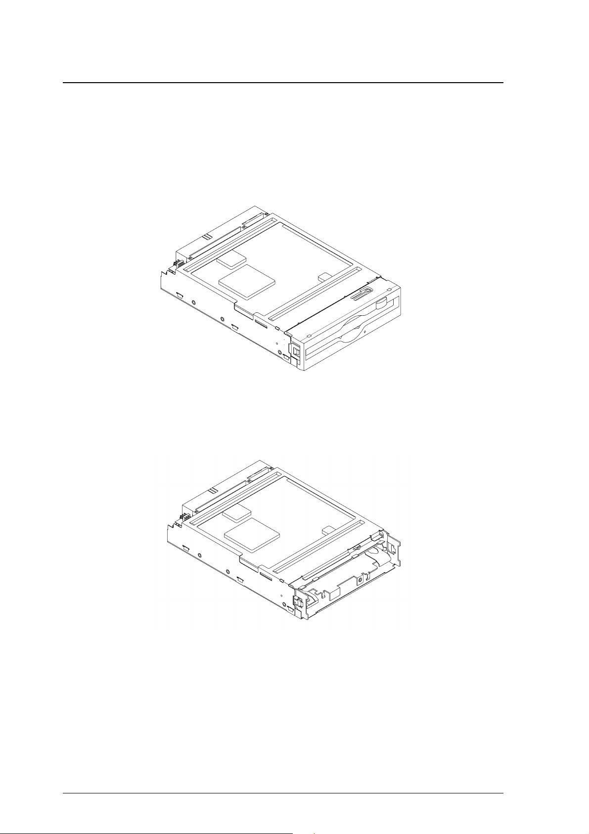
Figures 1.1 and 1.2 show the optical disk drive.
Figure 1.1 The optical disk drive (with panel)
Figure 1.2 The optical disk drive (without panel)
1-6 C156-E227-01EN
Page 29
1.2.2 Configuration
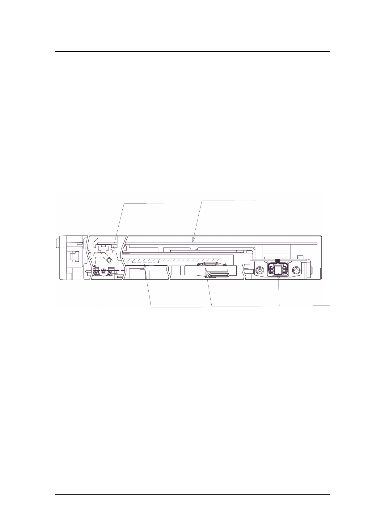
Figure 1.3 shows the configuration of the optical disk drive.
The optical disk drive consists of a mechanical section, a fixed optics section, a
control circuit section, and an actuator.
The mechanical section includes the spindle motor, actuator section, bias magnet,
and cartridge holder vertical motion mechanism.
The fixed optics section consists of the optical components, position detector, and
LD controller.
The control circuit section includes the drive control circuit section and I/F circuit
section.
1.2 Configuration of Optical Disk Drive
Mechanical section
Spindle motor Actuator
Figure 1.3 Configuration of optical disk drive
1.2.3 Mechanical section
(1) Loading and ejecting an optical disk cartridge
Control circuit section
Fixed optics section
The optical disk drive includes a cartridge load mechanism and an auto eject
mechanism. If an optical disk cartridge is manually inserted in the drive's slot as
far as it will go, the cartridge load mechanism automatically lowers the cartridge
and mounts it on the spindle motor. If the Eject button on the front panel is
pressed, the auto eject mechanism automatically ejects the cartridge.
(2) Spindle motor
An optical disk cartridge hub and the spindle motor shaft are magnetically
combined. Therefore, a disk rotates as fast as the spindle motor shaft rotates. The
spindle motor, a DC brushless motor, provides high-speed rotation at 5,455 rpm
and 3,637 rpm and high-accuracy rotation at ± 0.1%.
C156-E227-01EN 1-7
Page 30

General Description
(3) Actuator section
The actuator section consists of a focus actuator and a tracking actuator. The
former focuses a laser beam on the surface of an optical disk while the latter
moves the beam spot along the radius, on the surface of an optical disk (seek
operation).
The actuator section is directly driven by a linear voice coil motor. The tracking
actuator is based on the pulse-width modulation (PWM) system and realizes low
power consumption and high-speed access.
(4) Separate optical sections
The optical head section has a split structure in which the fixed optics section is
separated from the moving optics section to minimize seek time and positioning
error. This reduces the weight of the moving parts.
The fixed optics section consists of the laser diodes, collimator lens, separation
prism, condensing lens, and the optical detector.
A laser diode for recording and playback transmits one laser beam to the actuator
section.
(5) Panel
The central part of the panel is hollowed out to provide enough space to enable
the cartridge to be inserted by pushing it with a finger, thereby facilitating
insertion.
The panel is also simply designed using an eject button that also serves as LED
light emitting part.
1.2.4 Control circuit section
Figure 1.4 is a block diagram of the control circuit section and the peripheral
sections.
1-8 C156-E227-01EN
Page 31

1.2 Configuration of Optical Disk Drive
ATAPI
I/F
Main control section
MPU
ODC
DSP
User Logic
LSI i/f
F-ROM
D-RAM
Driver section
Read Amp
Power Amp
Filter
Sensor
Motor Driver
Head section
Laser Diode
Photo Diode
APC Amp
LPC Amp
Head Amp
Actuator section
Focus Act.
Track Act.
Spindle Motor
Temperature Sensor
Bias Coil
Eject Motor
Cartridge Sensor
Figure 1.4 Block diagram of the control circuit section
DE
The control circuit section is divided roughly into two parts: an ATAPI controller
section that controls between the ATAPI interface and drive interface, and a drive
circuit section that controls the drive section.
(1) ATAPI controller circuit section
The ATAPI controller circuit, which uses an LSI for improved reliability, controls
the drive through ATAPI interface control, read-write control, beam control, etc.,
by using one high-speed microprocessor (MPU).
(2) Drive circuit section
The drive circuit section consists of the laser diode light emitting control circuit,
signal reproduction circuit, servo/seek control circuit, rotation control circuit, and
other control circuits. In particular, the servo/seek control circuit consists of a
DSP (digital signal processor) for circuit reduction and the realization of a simple
configuration.
The drive circuit section performs the seek, erase, record, and playback operations
while controlling the focus tracking of the beam.
C156-E227-01EN 1-9
Page 32

This page is intentionally left blank.
Page 33

CHAPTER 2 Specifications
2.1 Specifications of Optical Disk Drives
2.2 Specifications of Optical Disk Cartridges
2.3 Defect Management
This chapter provides the specifications of the optical disk drives and the optical
disk cartridge.
2.1 Specifications of Optical Disk Drives
2.1.1 Catalog and order numbers
Table 2.1 lists the model names (catalog numbers) and order numbers of optical
disk drives.
Table 2.1 Representative model names and order numbers
Model name
(catalog number)
MCM3064AP CA06086-B331 With panel Light gray
MCM3130AP CA06123-B331 With panel Light gray
Order No. Panel Panel color Mounting screws
(2.5Y 7.2/0.4)
(2.5Y 7.2/0.4)
Metric screws (M3)
Metric screws (M3)
C156-E227-01EN 2-1
Page 34

Specifications
2.1.2 Specifications of drives
Table 2.2 lists the specifications of MCM3064AP, MCM3130AP optical disk
drives.
Table 2.2 Specifications (1 of 2)
[MCM3064AP, MCM3130AP]
Item Specifications
Optical disk media 128 MB media 230 MB media 540 MB media 640 MB media 1.3 GB media (*6)
Storage capacity
(one side)
Capacity per
track
Capacity per
sector
Number of user tracks/side (*1) 10,000 17,940 42,042 18,480 36,855
Number of alternate sectors/side ≤1,024 ≤1,025 ≤2,250 ≤2,244 ≤4,437
Number of sectors/track 25 25 25 17 17
Data transfer rate 1.65 MB/s
Average seek time (*2) 23 ms (typ)
Average latency
Rotational speed
Heads
Positioner type
Servo tracking method
Recording density
Loading time (*3)
Unloading time (*4)
Load/unload life
Host interface
Transfer mode
Data transfer rate
Unformatted 181 MB 325 MB 819 MB 818 MB 1.688 GB
Formatted 128 MB 230 MB 538 MB 643 MB 1.283 GB
Unformatted 18,100 bytes 18,100 bytes
Formatted 12,800 bytes 12,800 bytes
Unformatted 725 bytes 725 bytes 778 bytes 2,584 bytes 2,631 bytes
Formatted 512 bytes 512 bytes 512 bytes 2,048 bytes 2,048 bytes
(maximum)
0.39 MB/s
continuous
writing
(execution)
1.16 MB/s
continuous
reading
(execution)
5.5 ms 8.2 ms
5,455 rpm ±0.1% 3,637 rpm ±0.1%
Positioner + Separated optical components
1 (Linear voice coil motor)
ISO continuous servo method
24,424 bpi
(1.04µm/bit)
15,875 TPI
8 sec. (typ) 12 sec. (typ)
4 sec. (typ)
20,000
ATAPI (conforming to the ATA/ATAPI-5 standard)
PIO mode 4, multiword DMA mode 2, and Ultra-DMA mode 2
PIO mode: 16.6 MB/s
Multiword DMA mode 2: 16.6 MB/s
Ultra-DMA mode 2: 33.3 MB/s
(logical track
capacity)
(logical track
capacity)
2.00 to 3.16 MB/s
(maximum)
0.47 to 0.75 MB/s
continuous
writing
(execution)
1.40 to 2.23 MB/s
continuous
reading
(execution)
29,308 bpi
(0.87µm/bit)
18,275 TPI
19,450 bytes
(logical track
capacity)
12,800 bytes
(logical track
capacity)
3.54 to 5.94 MB/s
(maximum)
0.78 to 1.30 MB/s
continuous
writing
(execution)
2.33 to 3.91 MB/s
continuous
reading
(execution)
52,900 bpi
(0.48µm/bit)
23,090 TPI
43,928 bytes
(logical track
capacity)
34,816 bytes
(logical track
capacity)
3.52 to 5.87 MB/s
(maximum)
0.93 to 1.55 MB/s
continuous
writing
(execution)
2.79 to 4.66 MB/s
continuous
reading
(execution)
45,798 bytes
(logical track
capacity)
34,816 bytes
(logical track
capacity)
3.92 to 6.70 MB/s
(maximum)
0.99 to 1.70 MB/s
continuous
writing
(execution)
2.98 to 5.09 MB/s
continuous
reading
(execution)
89,100 bpi
(0.285µm/bit)
28,200 TPI
2-2 C156-E227-01EN
Page 35

2.1 Specifications of Optical Disk Drives
Table 2.2 Specifications (2 of 2)
Item Specifications
Optical disk media 128 MB media 230 MB media 540 MB media 640 MB media 1.3 GB media (*6)
Data buffer
Error correction (*5)
1,844 KB
Correctable up to 8-byte/interleave
Bit error rate: 10
-12
or less
*1 The number of user tracks indicates the maximum user zone which includes
the spare area and slipping area.
*2 Mathematical average of 1,000 times of random seek, which does not
include command overhead or track address recognition time.
Furthermore, it may depend on the quality of the media and the drive
installation environment.
*3 Loading time is the time that elapses from the time an optical disk cartridge
is inserted, to the time the optical disk drive is ready for processing of an
access command.
*4 Unloading time is the time that elapses from the time the eject button is
pressed or the eject command is issued, to the time an optical disk cartridge
is ejected.
*5 The bit error rate must be 10
10
-4
or less.
-12
or less using a disk whose raw error rate is
*6 The MCM3064AP does not support 1.3-gigabyte MO disks.
C156-E227-01EN 2-3
Page 36

Specifications
2.1.3 Environmental and power requirements
Table 2.3 lists the environmental and power requirements.
Table 2.3 Environmental and power requirements (1 of 2)
Item Specification
Power
requirements
Power Ready 3.9 W (typ) (*2)
consumption Random seek, read or write 5.8 W (typ) (*2)
(Average) Power save
Outer
dimensions
(WKDKH) Without panel 101.6K148.4K25.4 mm
Weight 410 g (with panel)
Environmental
requirements
Average +5 VDC±5% 1.2 A (2.7 A max) (*1)
Ripple requirement 100mV pp (DC-1 MHz)
Pre-idle mode
mode
With panel 101.6K150.0K25.4 mm
Operating
Idle mode
Standby mode
Sleep mode
3.9 W (typ) (*2)
2.0 W (typ) (*2)
1.2 W (typ) (*2)
1.2 W (typ) (*2)
Temperature: 5 to 45°C (gradient 15°C /h or less)
(*3)
Relative humidity: 10 to 85% (No condensation)
Maximum wet bulb temperature: 29°C or lower
Idle
Temperature: 0 to 50°C
Relative humidity: 10 to 85% (No condensation)
Maximum wet bulb temperature: 36°C or lower
Transport
Temperature: –40 to 60°C (24 hours or less)
Temperature: –20 to 60°C (24 hours or more)
Relative humidity: 5 to 90% (No condensation)
Maximum wet bulb temperature: 41°C or lower
Installation Tilt angle –5° to +10° (*3)
2-4 C156-E227-01EN
Page 37

2.1 Specifications of Optical Disk Drives
Table 2.3 Environmental and power requirements (2 of 2)
Item Specification
Vibration/
shock
Altitude Operating 3,000 m (10,000 ft) or less
Ambient
cleanliness
Operating 3.92 m/s2{0.4 G} (5 to 500 Hz, Sine Sweep)
Shock 19.6 m/s
Idle
No cartridge, power ON
Transport Shock 490 m/s
Idle 12,000 m (40,000 ft) or less
Air flow Not required
Air purity General office environment or better
Shock 49 m/s
Requirement: Packing specifications specified by Fujitsu
(dust particle level: Class 5 million or less particle level)
9.8 m/s2{1.0 G} (5 to 500 Hz, Sine Sweep)
2
{2 G} (10 ms, Half Sine Pulse)
2
{5 G} (10 ms, Half Sine Pulse)
2
{50 G} (10 ms, Half Sine Pulse)
*1 During random seek or read/write but excluding pulse waveform at 500 µs
or less
*2 Average value at an ambient temperature of 25°C and a voltage of 5 V
*3 The performance is specified at an ambient temperature of 25°C and level
placement at 0°.
Note:
1. The current limiter value on the power supply must not exceed 5 A.
2. The specifications for during transport are under the packaging conditions
specified by Fujitsu.
3. Note that, concerning the power requirements, a voltage drop may occur
depending on the power cable in use.
2.1.4 Error rate
Data blocks to be accessed should be evenly distributed on the disk. Errors due to
disk defects are not included.
(1) Bit error rate after ECC processing
The error rate after ECC processing must be 10-12 or less. An optical disk whose
raw error rate is 10-4 or less should be used.
(2) Positioning error rate
The positioning error rate must be 10-6 or less (with retry).
C156-E227-01EN 2-5
Page 38

Specifications
2.1.5 Reliability
(1) Mean time between failures (MTBF)
The MTBF is 120,000 hours or more. Failures due to disk errors are not included.
Conditions
•
Power-on time: 200 hours/month or less
•
LD-on time: 20% or less of power-on time
•
Ambient temperature: 25°C
Note: The MTBF is defined as follows:
Total operating time in all fields (hours)
MTBF =
Number of device failure in all fields
1) Operating time is the total time in which power is supplied.
(2) Service Life
2) Device failures include failures requiring repair, readjustment, or
replacement. However, they do not include failures that are not due to the
optical disk drive itself but to external factors such as careless device
handling, nonsupport of environmental requirements, power failures, host
system errors, and interface cable errors.
This drive will not require overhaul within the first five years of installation if
properly maintained (both disk media and optical parts cleaned) and handled as
recommended.
Data loss:
Data is not guaranteed if a power failure occurs or the I/F cable is
pulled out while:
• Data is being written to a data block
• A disk is being initialized (formatted)
• Defect processing is in progress
Data is not guaranteed either if the drive is moved with the optical
disk cartridge inserted or the drive is exposed to excessive shock or
vibration.
2-6 C156-E227-01EN
Page 39

2.2 Specifications of Optical Disk Cartridges
2.2 Specifications of Optical Disk Cartridges
2.2.1 Recommended optical disk cartridges
Optical disk cartridges basically comply with the ISO/IEC 10090 standard for 128
MB capacity, ISO/IEC 13963 standard for the 230 MB capacity, and ISO/IEC
15041 standard for the 540 and 640 MB capacity.
Table 2.4 shows the specifications of the optical disk cartridges recommended for
this optical disk drive. The specified drive performance may not be obtained if
other disk cartridges are used.
Table 2.4 Recommended opti cal disk cartridges
Model Model number Drawing number
Optical disk cartridge (128 MB) 0242110 CA90002-C010
Optical disk cartridge (230 MB) 0242210 CA90002-C011
Optical disk cartridge (540 MB) 0242410 CA90002-C012
Optical disk cartridge (640 MB) 0242610 CA90002-C013
Optical disk cartridge (1.3 GB) 0242810 CA90002-C015
Overwrite optical disk cartridge (230 MB) 0242310 CA90002-C041
Overwrite optical disk cartridge (540 MB) 0242510 CA90002-C042
Overwrite optical disk cartridge (640 MB) 0242710 CA90002-C043
C156-E227-01EN 2-7
Page 40

Specifications
2.2.2 Appearance
Figure 2.1 shows an optical disk cartridge. The names of the components of an
optical disk cartridge are also shown.
(a) Shutter closed
(2) Shutter
(1) Cartrige case
(b) Shutter open
(3) Write protect tab
Figure 2.1 Optical disk cartridge (1/2)
(4) Disk
(5) Hub
Figure 2.1 Optical disk cartridge (2/2)
2-8 C156-E227-01EN
Page 41

2.2 Specifications of Optical Disk Cartridges
The following explains the components of the optical disk cartridge shown in
Figure 2.1.
1) Cartridge case
The disk housing is provided to protect the disk from damage when handling
it, and facilitates replacement of the disk.
The cartridge case has a label and a write protect tab on it.
2) Shutter
The shutter protects the disk from contamination. This metallic door opens
when the cartridge is inserted into the optical disk drive.
3) Write protect tab
Slide the write protect tab to enable or disable writing to the disk.
4) Disk
Stores data that can be read or written using a laser beam.
5) Hub
The hub is the central disk part to be connected to the spindle of the optical
disk drive.
The hub is used for radial centering and axial positioning.
C156-E227-01EN 2-9
Page 42

Specifications
2.2.3 Specifications of disk
Table 2.5 lists the disk specifications.
Table 2.5 Disk specifications
Item Specification
Reliability Read cycle >10
Erase/write/read cycle >10
Load/nload cycle 25,000
Archival life (in accordance with
>10 years (*1)
acceleration test results)
Shelf life (in accordance with acceleration
>10 years (*2)
test results)
Environmental
Operating temperature 5 to 55°C
requirements
Operating relative humidity 3 to 85% RH (*3)
Storage temperature –20 to 55°C
Storage humidity 3 to 90% RH (*3)
*1 Archival life indicates the maximum period during which recorded
information can be read from a disk.
*2 Shelf life indicates the maximum period during which information can be
written to an unrecorded disk.
8
6
*3 Maximum wet bulb temperature = 29°C.
Note: Non-recommended disks, if used, must be subject to a compatibility check
by the customer.
2-10 C156-E227-01EN
Page 43

(1) 128 MB media
The ISO/IEC10090 defines 128-MB media specification.
(2) 230 MB media
The ISO/IEC13963 defines 230-MB media specification.
(3) 540 MB/640 MB media
The ISO/IEC15041 defines 540 MB/640 MB media specification.
(4) 1.3 GB media
The Cherry Book version 1.0 defines 1.3 GB media specification.
2.3 Defect Management
2.3.1 Defect management schematic diagram
2.3 Defect Management
Defective sectors on the disk must be replaced with good sectors in accordance
with the defect management scheme as follows: Sectors found defective during
surface inspection are handled using a sector slipping algorithm. Sectors found
defective after initialization are replaced using a linear replacement algorithm.
Figure 2.2 shows the sector slipping and linear replacement algorithms.
(a) Sector slipping algorithm (b) Linear replacement algorithm
Figure 2.2 Algorithms for alternate processing
C156-E227-01EN 2-11
Page 44

Specifications
During initialization, the user area is divided into several groups. Each of the
groups contains data sectors and spare sectors. Spare sectors are used as
replacements for defective data sectors. During initialization, the surface
inspection over the user area can be performed.
Figure 2.3 shows an example of alternate processing.
Figure 2.3 Example of alternate processing
2-12 C156-E227-01EN
Page 45

CHAPTER 3 Installation Requirements
g
3.1 Environmental Requirements
3.2 Mounting Requirements
3.3 Power supply Requirements
3.4 Cable Connections
3.5 Jumper Settings
3.6 Precautions on Handling the Drive
3.7 Mounting the Drive
3.8 Cable Connections
3.9 Post-installation Operation Check and Preparation for Use
3.10 Demountin
This chapter describes environmental, mounting, power supply, and connection
requirements.
the Drive
3.1 Environmental Requirements
The optical disk drive must be installed in an environment complying with the
ambient environmental requirements defined in Section 2.1.3.
3.1.1 Temperature measurement points
While the drive is operating, the ambient temperatures measured 3 cm away from
the surfaces of the optical disk drive must satisfy the ambient environmental
requirements specified in Section 2.1.3. As for the surface temperatures during
operation, the contact temperatures measured at the points shown in Figure 3.1
must satisfy the temperature requirements specified in Section 3.1.2.
C156-E227-01EN 3-1
Page 46

Installation Requirements
(a) Inside optical disk cartridge
Hole for inserting thermocouple
Figure 3.1 Surface temperature measurement point
3.1.2 Temperature requirements
Opening of disk outer wall
Tip of thermocouple
Table 3.1 shows the temperature requirement at the measurement point shown in
Figure 3.1.
Table 3.1 Temperature requirements at measurement points
Measurement point Maximum allowable surface temperature
Inside the cartridge 55°C (*1)
IC (controller) surface 95°C
IC (read amp.) surface 85°C
*1 60°C for the optical disk cartridges recommended by Fujitsu (except 1.3
GB).
The following describes a procedure for measuring the temperature inside a
cartridge.
1) At the bottom of the cartridge, open a hole large enough for the thermocouple
to be inserted as shown in Figure 3.1.
2) Disassemble the cartridge.
3) Cut off part of the wall surrounding the optical disk (disk outer wall) as shown
in Figure 3.1.
At this point, cut off a section 5 to 10 mm in width from the disk outer wall.
4) Using an adhesive agent, affix the tip of the thermocouple to the opening of
the disk outer wall.
3-2 C156-E227-01EN
Page 47

5) Pass the thermocouple through the hole in the cartridge and reassemble the
cartridge.
Using an adhesive agent, etc., fill any gap between the hole and the
thermocouple.
Note: The surface of the cartridge shown in Figure 3.1 has been cut away to
illustrate the elements inside the cartridge. Do not actually cut away the
surface.
If the external environment temperature rises above the specified value,
the drive will take protective action to deal with the temperature increase
by automatically placing an interval between commands before
responding to a command.
3.1.3 Temperature rise
Table 3.2 Temperatures at measuring points (Reference)
[Ambient temperature of the optical disk drive: 45°C] (°C)
Measurement point Random seek Criteria
Inside cartridge 54.0°C 55°C
IC (controller) surface
IC (read amp.) surface
Thermal sensor 54.2°C ––
Notes:
1. The above data was taken in a constant temperature chamber in which the
temperature around the optical disk drive was kept at 45°C. The data was not
taken with the drive installed in a box in which the drive is actually used.
2. Note that, when installed in a box, the ambient temperature around the drive
will differ depending on the air circulation conditions of the box, and the
temperature increase inside the cartridge will differ accordingly.
70.5°C 95°C
72.4°C 85°C
3.1.4 Air cleanliness
The air cleanliness in the device environment is expressed by the number of dust
particles per unit area. Fujitsu recommends using the optical disk drive in the
environment of class 5 million or less particle level. (Class 5 million: This means
there are 5 million dust particles of 0.5 ?m diameter or larger per cubic foot. This
is equivalent to 0.15 mg/m3.)
3.2 Mounting Requirements
3.2.1 Outer dimensions
C156-E227-01EN 3-3
Page 48

Installation Requirements
Figures 3.2 to 3.3 show the outer dimensions of the optical disk drive and the
positions of the mounting holes.
Figure 3.2 Outer dimensions (1/2)
3-4 C156-E227-01EN
Page 49

3.2 Mounting Requirements
Position after a cartridge is loaded
Bottom of
the frame
Position when loading a cartridge
Center of a cartridge when loaded
Figure 3.2 Outer dimensions (2/2)
C156-E227-01EN 3-5
Page 50

Installation Requirements
Figure 3.3 Outer dimensions (1/3)
3-6 C156-E227-01EN
Page 51

3.2 Mounting Requirements
Oblong hole: 2±0.1 (width)
× 2.5±0.1 (length)
(Width of C 0.5)
Details on D part
Figure 3.3 Outer dimensions (2/3)
Details of C part
(Stroke for the switch)
C156-E227-01EN 3-7
Page 52

Installation Requirements
Figure 3.3 Outer dimensions (3/3)
3-8 C156-E227-01EN
Page 53

3.2.2 Installation direction
Figure 3.4 shows the permissible installation directions for the optical disk drive.
The mounting angle tolerance must be within -5( to 10( relative to the horizontal
plane.
(-) shows that the cartridge insertion slot faces downward.
3.2 Mounting Requirements
Disk insertion slot
Horizontal
Vertical
(Two orientations)
Eject button/Busy LED
Manual eject hole
Figure 3.4 Installation directions
C156-E227-01EN 3-9
Page 54

Installation Requirements
3.2.3 Center of gravity
Figure 3.5 shows the center of gravity of the optical disk drive.
Figure 3.5 Center of gravity
3-10 C156-E227-01EN
Page 55

3.2.4 Precautions on mounting
(1) Mounting frame structure and clearance
a) For vibration resistance and heat dissipation, mount this optical disk drive
using a frame having an embossed structure shown in Figure 3.6 or a similar
structure providing an equivalent function.
b) A mounting screw must have an inward projection (entry depth) of 3 mm or
less from the outer surface of the mounting frame of the optical disk drive as
shown in Figure 3.6.
c) The upward-downward and left-right clearance between the external surface
of the mounting frame of the optical disk drive and the user's embossstructure frame must be at least 1.5 mm.
d) The floating clearance of the optical disk drive must be 1.5 mm or more.
e) When mounting the optical disk drive, the screw tightening torque must be 0.4
to 0.45Nm (4 to 4.6kgf-cm).
f) When the optical disk drive (with a panel) is mounted in a cabinet, there
should be no distortion or deformation in the target housing or the mounting
fittings. Furthermore, the optical disk drive's panel must not be deformed.
3.2 Mounting Requirements
If the drive is used with the panel deformed, ejection of the cartridge will be
faulty.
Make sure that the door closes from any position after mounting the optical
disk drive.
1.5 or
more
1.5 or
more
1.5 or
more
1.5 or
more
1.5 or
more
Optical disk drive
Optical disk drive
1.5 or
more
1.5 or
more
φ15
or less
Mounted on the side
1.5 or
more
3or
less
3orless
(Unit: mm)
φ15
or less
Mounted on the bottom
Figure 3.6 Mounting frame structure
C156-E227-01EN 3-11
Page 56

Installation Requirements
(2) Checking the panel function
There must not be any deformation in the panel after the optical disk drive is
installed in a cabinet. Make sure that the door of the disk insertion slot closes
from any location with the drive installed in the cabinet.
(3) Service areas
Figure 3.7 shows the locations that need to be accessed for installation, and after
installation is carried out.
[P side]
- Cable connection
[R side]
- Monitoring screw hole
- Monitoring screw hole
`
(4) External magnetic fields
Mount the optical disk drive away from powerful magnetic materials (e.g., a
speaker) to avoid any adverse effects from external magnetic fields.
(5) Leak magnetic field
The VCM drive magnetic circuit may leak a magnetic field (Up to 2.5 mT at a
distance of 4 mm from the drive surface).
[Q side]
Figure 3.7 Service areas
Do not place any devices sensitive to a magnetic field near the
optical disk drive.
3-12 C156-E227-01EN
Page 57

(6) External light source
Mount the optical disk drive away from strong light sources (e.g., camera flash).
(7) System ground (handling of SG and FG)
The optical disk drive must be grounded to the signal ground (SG) of the power
supply of the user's system. This SG line must be supplied with the system as well
as the power line.
The optical disk drive can be mounted in a 120 mm (5 inch) device
bay of the PC chassis using either a metal frame or a plastic
(nonconductive material) frame.
If a plastic frame is used, the personal computer's FG and the optical
disk drive's FG are not shorted. Consequently, the static electricity
tolerance is inferior to that realized when a metal frame is used.
Fujitsu recommends using a metal frame. In particular, a metal
frame must be used especially when high static electricity tolerance
is required.
3.3 Power Supply Requirements
3.3 Power Supply Requirements
(1) Allowable input voltage and current
The DC power supply input voltage must satisfy the requirements described in
Section 2.1.3, "Environmental and power requirements" when measured at the
power supply connector pin (receiving end) of the optical disk drive (For other
requirements, see items (4) and (5) below).
(2) Current waveform (reference)
Figure 3.8 shows the current waveform while a disk is inserted.
Figure 3.8 MCM3130AP current waveform (+5 VDC)
C156-E227-01EN 3-13
Page 58

Installation Requirements
3.4 Cable Connections
3.4.1 Drive connectors
The optical disk drive (ODD) has the following connectors. Figure 3.9 shows the
location of the connectors.
- AT interface connector (40 pins) and power connector (4 pins) CN1
Power connector
1 +12 VDC or no connection
2 +12 VDC return (GND) or no connection
3 +5 VDC RETURN (GND)
4 +5 VDC
Figure 3.9 Connector and terminal locations
3-14 C156-E227-01EN
Page 59

3.4 Cable Connections
3.4.2 Cable connector specifications
Table 3.3 lists the recommended cable connector specifications.
Table 3.3 Cable connector specifications
Cable name Name Model name Vendor
AT interface cable (40
pins)
Power cable
Cable socket (closed
end type)
Cable socket
(through end type)
Signal cable 445-248-40 SPECTRS STRIP
Cable socket housing 1-480424-0 AMP
Contact 170121-4 AMP
Signal cable AWG18
Use a cable that is flat over the whole length as the host interface
cable (do not use a cable with only the crimp section flat, with
separate conductors from halfway, or with twisted pair type
conductors).
FCN-707B040-AU/B Fujitsu
FCN-707B040-AU/0 Fujitsu
C156-E227-01EN 3-15
Page 60

Installation Requirements
3.4.3 Drive connections
Figure 3.10 shows cable connections between devices.
Host
system
Figure 3.10 Cable connection diagram
3.5 Jumper Settings
3.5.1 Factory shipment settings
Figure 3.11 shows the jumper wire settings at factory shipment.
CNH5
5
31
Drive 1
Drive 2
DC powerIDE cable
Power
supply
: Connected
642
5-6 (connected): Master device setting
Figure 3.11 Jumper wire settings at factory shipment
3-16 C156-E227-01EN
Page 61

3.5.2 Mode settings
(1) Master device mode setting
Figure 3.12 shows the setting that enables a master device (device 0) to be
detected.
Figure 3.12 Master device setting
3.5 Jumper Settings
CNH5
531
642
(2) Slave device mode setting
Figure 3.13 shows the setting that enables a slave device (device 1) to be detected.
Figure 3.13 Slave device setting
CNH5
531
642
C156-E227-01EN 3-17
Page 62

Installation Requirements
(3) Cable selection mode setting
Figure 3.14 shows the master/slave device setting that is set by connecting the
CSEL signal line to the interface. The special interface connector shown in the
example in Figure 3.14 is also required.
Figure 3.14 Cable selection mode setting
CNH5
531
642
Figure 3.15 shows an example of cable selection with the special interface cable.
In the figure, master CSEL is connected to the cable-side CSEL line (conductor)
and then connected to GND. By this, the master drive detects itself as a master.
At the same time, the slave device detects itself as a slave because the conductor
of slave CSEL is removed and slave CSEL has no connection to cable-side CSEL.
CSEL conductor
GND
Host system Master device Slave device
Example (1)
CSEL conductor
GND
Open
Open
Host system Master device Slave device
Example (2)
Figure 3.15 Cable selection example
3-18 C156-E227-01EN
Page 63

3.6 Precautions on Handling of Drive
(1) General precautions
Keep the following points in mind to ensure the performance and reliability of the
optical disk drive:
Device damage:
1) Do not expose to the drive any shock or vibration exceeding the
specification because it will fatally damage the drive. Be
particularly careful of this point when unpacking the drive.
2) Do not leave the drive in a dirty or contaminated environment.
3) Since the drive contains CMOS components that may be
destroyed by static discharge, keep the following points in mind
after unpacking:
3.6 Precautions on Handling of Drive
(2) Unpacking the drive
a) Find a level work space. Place the carton properly on the floor by making
sure that the UP label on the carton is pointing upward. Handle the drive on a
soft surface such as a rubber mat, not on a hard surface such as a desk.
b) When removing the cushions, be careful not to apply excessive force to the
drive inside.
c) When removing the drive from the antistatic bag, be extra careful not to apply
excessive force to the printed circuit board unit surface and interface
connectors.
•
Use an antistatic mat and wear a wrist strap when handling the
drive.
•
Hold the mounting frame when handling the drive. Do not touch
the printed wiring board unit except when required to make the
settings.
4) When handling the drive, hold both sides of the mounting
frame. When touching any part of the drive other than both
sides of the mounting frame, avoid applying force on the
location.
5) When handling the drive or making settings, do not press hard
on the tip of the header pin of the printed circuit board unit.
d) When moving the drive to any location 10 degrees hotter or colder than the
temperature at the current location, leave the drive in the new location for at
least two hours before unpacking it.
C156-E227-01EN 3-19
Page 64

Installation Requirements
(3) Installation
a) While the power is on, do not connect or disconnect the connectors or change
the terminal settings.
b) While the power is on, do not move the drive.
c) Before moving the drive, first eject and remove any optical disk cartridge in it
andthenturnoffthepower.
Device damage: Before moving the drive, remove any optical disk cartridge in
it. If the drive is moved with the optical disk cartridge loaded in it, the head may
move back and forth in the drive to damage the head or disk, consequently
disabling data from being read later.
(4) Packing
a) Remove an optical disk cartridge from the drive before packing it.
b) Place the drive in an antistatic plastic bag with a desiccant (silica gel).
c) Fujitsu recommends using the same cushions and carton supplied by Fujitsu
with the drive. If they are not available, ensure the use of a carton with an
adequate shock absorbent structure that can prevent shock or vibration from
being directly applied to the drive. In this case, provide sufficient protection
on the printed circuit board unit surface and the interface connectors to avoid
damages.
d) Apply "UP" and "Handle With Care" labels to the outside of the package.
Figure 3.14 gives an overview of packing drives individually or in sets. Note that
different cushions of different forms and materials but with equivalent functions
maybeusedwhenpackingdrivesinthefuture.
3-20 C156-E227-01EN
Page 65

Holder
3.6 Precautions on Handling of Drive
Drive
Desiccant
Ejecting jig
Box
Packing box for
each individual
unit
Figure 3.16 Packing styles (1/2)
C156-E227-01EN 3-21
Page 66

Installation Requirements
Drive
Ejecting jig
Desiccant
Holder
Carton of
packing boxes
Figure 3.16 Packing styles (2/2)
3-22 C156-E227-01EN
Page 67

(5) Transportation
a) In principle, transport the drive while it is packed with the UP sign pointing
upward.
b) Transport the drive, after it is unpacked, only for a short distance. While
doing so, use cushions to avoid applying shock and vibration. Transport the
drive, after it is unpacked, in one of the orientations described in Section
3.2.2, "Installation orientation." (The horizontal orientation is recommended.)
(6) Storage
a) Use moisture-proof packing when storing the drive.
b) The storage environment must satisfy the requirements during non-operation
specified in Section 2.1.3, "Environmental and power requirements."
c) To prevent condensation, avoid exposing the drive to extreme temperature
changes.
3.7 Mounting of Drive
3.7 Mounting of Drive
3.7.1 Mounting procedure
The method of and procedure for mounting the drive vary depending on the
system cabinet structure, etc. Determine the mounting procedure in accordance
with the requirements of your system.
This section describes the general mounting procedure and check items.
See Section 3.2, "Mounting Requirements" for details on mounting the optical disk
drive.
1) Tighten four mounting screws to secure the drive in the system cabinet.
•
The drive has ten mounting holes (both sides: 3 ( 2, bottom: 4). Secure the
drive by using the four mounting holes on either of the two sides or the
bottom.
•
Use mounting screws whose entry depth is 3 mm or less from the outer
surface of the mounting frame of the drive after they are tightened. (See
Figure 3.6)
•
When mounting the drive with screws, the screw tightening torque should be
0.4 to 0.45Nm (4 to 4.6kgfcm).
•
Be extra careful not to damage the parts on the printed circuit board unit while
you mount the drive.
2) After securing the drive, make sure that the drive does not come into contact
with the chassis of the system cabinet. There must be at least a 1.5-mm
clearance between the drive and the chassis. (See Figure 3.6.)
C156-E227-01EN 3-23
Page 68

Installation Requirements
3.8 Cable Connections
Use the following cables to connect the optical disk drive to the system. See
Section 3.4, "Cable Connections" for details on the connector positions and cable
connection requirements.
•
Power supply cable
•
AT interface cable
The general procedure for and precautions on connecting cables are given below.
Be extra careful regarding the insertion direction of each cable connector.
Device damage:
- Make sure that the system power is off.
- Do not connect or disconnect any cable while the drive power is on
1) Connect the power cable.
2) Connect the AT interface cable.
3) After inserting the connector of a cable, hold the cable properly so that it
neither touches a part on the device and PC board unit nor prevent the cooling
air from flowing in the system cabinet.
3.9 Post-installation Operation Check and Preparation for Use
3.9.1 Initial operation check
This section provides the operation check procedures after power-on.
(1) Initial operation upon power-on
•
When the power is turned on, the drive starts initial self-diagnostics. The
LED on the front panel is on for 1 second during initial self-diagnostics.
•
If an error is detected during initial self-diagnostics, the LED on the front
panel blinks. If the initial self-diagnostics normally terminates, the LED goes
off.
•
If the power is turned on with no cartridge inserted, the eject motor
automatically turns once.
3-24 C156-E227-01EN
Page 69

3.9 Post-installation Operation Check and Preparation for Use
(2) Items to confirm if an error occurs in initial self-diagnostics
•
Make sure that the cables are correctly connected.
•
Make sure that the power voltage is supplied normally. (Measure the voltage
at the power supply connector of the optical disk drive.)
•
Make sure that all of the setting terminals are correctly set.
•
Continuous blinking of the LED on the front panel indicates that an error has
been detected during initial self-diagnostics. Fujitsu recommends issuing,
wherever possible, the REQUEST SENSE command from the initiator (host
system) to collect information (sense data) for error analysis.
The LED is on while the optical disk drive is performing the seek,
write, or read operation. However, because an LED goes on only
momentarily, it may seem to blink or remain off.
Upon power-on, the eject motor turns once to correct the position of
the eject motor (in case it deviates due to shock or vibration applied
to the drive during transportation), and allows a cartridge to be
inserted normally.
If you cannot insert a cartridge properly, remove the cartridge and
turn on the drive power to have the eject motor turn once before
reinserting the cartridge.
3.9.2 Connection check
When the initial operation check terminates normally after power-on, check
whether the drive is correctly connected by issuing a command from the host
system. The checking procedure depends on the host system configuration. The
following describes a general check procedure.
(1) Check to be made if the initial operation check terminates abnormally:
a) Analyze sense data if any has been collected due to the REQUEST SENSE
command. If the error is recoverable, retry the processing.
b) On AT interface cable connections, make sure that:
•
All connectors, including those of other devices, are correctly connected.
•
Correct cables are being used (whether they support the cable selection mode
setting).
c) Reconfirm that the jumper wire settings are correct.
C156-E227-01EN 3-25
Page 70

Installation Requirements
3.10 Demounting of Drive
The procedure for demounting an optical disk drive (to check the setting terminals,
change the settings, or replace the drive, for example) depends on the system
cabinet configuration. Determine the demounting procedure by considering the
requirements unique to your system. This section describes the general
demounting procedure and precautions to follow when demounting a drive.
Device damage: Before demounting the optical disk drive, turn
off the system power. While the power is on, do not remove screws
securing the cables and drive.
1) Remove the power cable.
2) Remove the AT interface cable.
3) Remove the four screws securing the drive, then remove the drive from the
system cabinet.
4) While storing or transporting the drive, put the drive into an antistatic bag.
(See Section 3.6.)
3-26 C156-E227-01EN
Page 71

CHAPTER 4 Host Interface
4.1 Pin Assignment
4.2 Signal Description
4.3 Interface Registers
4.4 Various Processes
4.5 ATA Commands
4.6 Packet Commands
4.7 Timing
This chapter describes host interface specification.
C156-E227-01EN 4-1
Page 72

Host Interface
4.1 Pin Assignment
The table below lists pin assignments of the interface connector.
Although the MCG3xxxAP has power-related pins, they are omitted in this
specification.
Table 4.1 Connector pin assignments (1/2)
Description PIN Signal name
Reset 1 RESETGround 2 Ground
Data bus bit 7 3 DD7
Data bus bit 8 4 DD8
Data bus bit 6 5 DD6
Data bus bit 9 6 DD9
Data bus bit 5 7 DD5
Data bus bit 10 8 DD10
Data bus bit 4 9 DD4
Data bus bit 11 10 DD11
Data bus bit 3 11 DD3
Data bus bit 12 12 DD12
Data bus bit 2 13 DD2
Data bus bit 13 14 DD13
Data bus bit 1 15 DD1
Data bus bit 14 16 DD14
Data bus bit 0 17 DD0
Data bus bit 15 18 DD15
Ground 19 Ground
(keypin) 20 Reserved
DMA Request 21 DMARQ
Ground 22 Ground
I/O Write
Stop during Ultra DMA data bursts
Ground 24 Ground
4-2 C156-E227-01EN
23 DIOW-
STOP
Page 73

Table 4.1 Connector pin assignments (2/2)
4.1 Pin Assignment
I/O Read
DMA ready during Ultra DMA data in bursts
Data strobe during Ultra DMA data out bursts
Ground 26 Ground
I/O Ready
DMA ready during Ultra DMA data out bursts
Data strobe during Ultra DMA data in bursts
Cable Select 28 CSEL
DMA Acknowledge 29 DMACKGround 30 Ground
Interrupt Request 31 INTRQ
16 Bit I/O 32 IOCS16Device Address Bit 1 33 DA1
PASSED DIAGNOSTICS
Cable assembly type identifi er
Device Address Bit 0 35 DA0
25 DIOR-
HDMARDYHSTROBE
27 IORDY
DDMARDYDSTROBE
34 PDIAG-
CBLID-
Device Address Bit 2 36 DA2
Chip Select 0 37 CS0Chip Select 1 38 CS1Device Active or Slave (Device 1) Present 39 DASPGround 40 Ground
C156-E227-01EN 4-3
Page 74

Host Interface
4.2 Signal Description
Table 4.2 Signal description (1/2)
PIN Signal name I/O Description
1 RESET- I Reset signal
3, 5, 7, 9, 11,
13, 15, 17, 18,
16, 14, 12, 10,
8, 6, 4
21 DMARQ O Data request signal for DMA transfer
23 DIOW-
25 DIOR-
27 IORDY
DD7-0
DD15-8
STOP
HDMARDYHSTROBE
DDMARDYDSTROBE
I/O The low-order bus is a 8-bit bidirectional bus signal for
exchanging the status, data, and control data between
the host and ODD.
The high-order bus is used for 16-bit data transfers only.
I Write st robe sig n al.
Indicates that transfer has ended at Ultra DMA transfer.
I Read strobe signal
Indicates that the host can receive Ultra DMA data at
Ultra DMA in transfer.
The ODD latches data at both edges of this signal at
Ultra data out transfer.
O This is the ready signal for the host computer. The ODD
uses this signal to request an extension of the transfer
cycle when it cannot prepare a response to a data
transfer request from the host computer in time.
Indicates that the ODD can receive Ultra DMA data at
Ultra DMA out transfer.
The host latches data at both edges of this signal at Ultra
data in transfer.
28 CSEL I Sets the ODD to the master (device 0) or slave (device
1).
Effective by jumpering.
29 DMACK- I Answer signal in response to DMARQ during DMA
transfer
31 INTRQ O Interrupt signal to the host
32 IOCS16- O Indicates that the ODD is ready for 16-bit transfer when
the host addresses the 16-bit data port during PIO
transfer.
36, 33, 35 DA2, 1, 0 O Address signal used by the host to address the ODD task
file register
34 PDIAG- I/O Used by the slave (device 1) to notify the master (device
0) that diagnostics ended
4-4 C156-E227-01EN
Page 75

4.2 Signal Description
Table 4.2 Signal description (2/2)
PIN Signal name I/O Description
37 CS0- O Select signal used to select the command block register
38 CS1- O Select signal used to select the control block register
39 DASP- I/O When reset, slave (device 1) output signal indicating
that the slave (device 1) exists. Otherwise, the signal
indicates that the master (device 0) and slave (device 1)
is performing mechanical operation or a failure
occurred.
2, 19, 22, 24,
26, 30, 40
Ground - Ground signal
C156-E227-01EN 4-5
Page 76

Host Interface
4.3 Interface Registers
4.3.1 I/O registers
This section provides the I/O register functions and mapping. Definitions of each
register vary depending on which ATA or ATAPI commands are used.
Table 4.3 I/O port functi ons and mapping
Address signal Function
CS0- CS1- DA2 DA1 DA0 READ (DIOR-) WRITE (DIOW-)
N N x x x High impedance state Ineffective
Control block register
N A 0 x x High impedance state Ineffective
N A 1 0 x High impedance state Ineffective
N A 1 1 0 Alternate Status Device Control
N A 1 1 1 Drive Address Ineffective
Command block register
AN0 00 Data
A N 0 0 1 Error ATA Features (ATA)
ATAPI Features (ATAPI)
A N 0 1 0 Sector Count (ATA)
ATAPI Interrupt Reason
(ATAPI)
A N 0 1 1 Sector Number
A N 1 0 0 Cylinder Low (ATA)
ATAPI Byte Count (bits 0-7) (ATAPI)
A N 1 0 1 Cylinder High (ATA)
ATAPI Byte Count (bits8-15) (ATAPI)
AN1 10 Device/Head (ATA)
ATAPI Block Device Select (ATAPI)
A N 1 1 1 ATAPI Status ATA Command
A A x x x Ineffective Ineffective
Ineffective
The letter A indicates that the bit is asserted, N indicates that the bit is negated,
and X indicates that the bit is ignored.
C156-E227-01EN 4-6
Page 77

4.3 Interface Register
4.3.1.1 Alternate Status register
This register contains the same information as that of the ATAPI Status register,
except that the ODD does not recognize interrupts when reading this register.
Therefore, the ODD does not clear the INTRQ signal and does not clear interrupts
during the pending.
Table 4.4 Bit definiti ons of Alternate Status register
765 4 3210
BSY DRDY
Reserved
(0b)
SERVICE DRQ
CORR
(0b)
Reserved
(0b)
CHECK Read
4.3.1.2 ATA Command register
This register contains a command to be passed to the ODD. The ODD starts
executing a command immediat ely af ter the co mm and is writ ten in thi s registe r.
For executable commands and required parameters, see Table 4.37.
4.3.1.3 Data register
The data register is used for data transfer. The data width is always 16 bits.
4.3.1.4 Device Control register
This register's bits are defined as shown below.
Table 4.5 Bit defi niti ons of Device Control register
76543210
Reserved Reserved Reserved Reserved Reserved
SRST nIEN 0 Write
•
Bits 7 to 3 are reserved. The ODD ignores all value sets in these bits.
•
SRST is a reset bit for host software.
•
nIEN is an enable bit for device interrupts to the host. When nIEN is 0 and
the device is selected, the INTRQ signal is enabled by the tri-state buffer.
When nIEN is 1 or the device is not selected, the INTRQ signal is in the highimpedance state.
C156-E227-01EN 4-7
Page 78

Host Interface
4.3.1.5 Drive Address register
This register's bits are defined as shown below.
Table 4.6 Bit definitions of Drive Address register
76543210
HiZ nWTG nHS3 nHS2 NhS1 nHS0 nDS1 nDS0 Read
•
HiZ is always in the high-impedance state.
•
nWTG indicates the status of the ODD internal data write control signal
(Write Gate).
•
nHS3 indicates a binary complement of bits 3 to 0 of the drive select register.
•
nDS1 is the device select bit for device 1. It is 0 when device 1 is selected.
•
nDS0 is the device select bit for device 0. It is 0 when device 0 is selected.
4.3.1.6 ATAPI Byte Count register
This register's bits are defined as shown below.
Table 4.7 Bit defi niti ons of ATAPI Byte Count register
76543210
Byte Count (Bits 7-0) R/W
Byte Count (Bits 15-8) R/W
•
This register is used for PIO transfer only. The ODD sets the byte count to be
transferred by the host in this register and sets DRQ to 1. The ODD does not
update this register until transfer star ts.
4-8 C156-E227-01EN
Page 79

4.3 Interface Register
4.3.1.7 ATAPI Block Device Select register
This register's bits are defined as shown below.
Table 4.8 Bit definiti ons of ATAPI Block Device Select register
76543210
Unused Unused Unused Dev Unused Unused R/W
•
Bits 7, 6, 5, 3, 2, 1, and 0 are not used. The ODD ignores all value sets in
these bits.
•
Dev indicates the device address. When Dev is 0, device 0 is selected and
when Dev is 1, device 1 is selected.
•
Logical unit numbers (LUNs) are not supported. The ODD ignores all such
set values.
4.3.1.8 Error register
This register indicates the statu s of the final comm and.
The value of this register is effective when the ERR bit of the Status register is 1 at
completion of a command other than EXECUTE DEVICE DIAGNOSTIC.
The value of this register indicates the diagnostic code at power-on, reset, and
execution of the EXECUTE DEVICE DIAGNOSTIC command. For details on
diagnostic codes, see Section 4.5.5.
Table 4.9 Bit definitions of Error register
76543210
Sense Key MCR
(0b)
•
For the Sense Key, see Table 4.99.
•
MCR (Media Change Requested) is not used. It is always 0.
•
ABRT (Aborted Command) indicates that the value of the ATA command
ABRT EOM
(0b)
ILI
(0b)
code or task file register is incorrect.
Read
•
EOM (End of Media) is not used. It is always 0.
•
ILI (Illegal Length Indication) is not used. It is always 0.
C156-E227-01EN 4-9
Page 80

Host Interface
4.3.1.9 ATA Features register
This register is used for the SET FEATURES command.
4.3.1.10 ATAPI Features register
This register's bits are defined as shown below.
Table 4.10 Bit definitions of ATAPI Features register
76543210
Reserved
•
All values in bits 7 to 2 are ignored.
•
OVERLAP is not used. The ODD ignores the value set in this bit.
OVERLAP
DMA Write
•
When DMA is 1, the ODD performs DMA transfer for data transfer.
4.3.1.11 ATA Sector Count register
This register is used for the SET FEATURES command.
4.3.1.12 ATAPI Interrupt Reason register
This register's bits are defined as shown below.
Table 4.11 Bit definitions of ATAPI Interrupt Reason register
76543 2 10
Reserved
(0b)
Reserved
(0b)
•
Reserved
(0b)
Reserved
(0b)
Reserved
(0b)
RELEASE I/O C/D Read
When RELEASE is 1, the ODD releases the ATA bus before a command
being executed is completed.
•
I/O indicates the direction of data transfer. See Table 4.12.
•
C/D indicates the type of transfer. See Table 4.12.
4-10 C156-E227-01EN
Page 81

Table 4.12 I/O and C/D
I/O C/D Meaning
0 1 Packet command transfer
1 0 Data or parameter transfer (from the ODD to the host)
0 0 Data or parameter transfer (from the host to the ODD)
1 1 The completion status in the Status register is effective.
4.3.1.13 Sector Number register
This register is not used. The ODD ignores all specified values.
4.3.1.14 ATAPI Status register
This register indicates the status of the ODD. It is updated to reflect the current
ODD status and the progress of the current command. When the BSY bit is 0,
other bits of the register are effective and some other command block registers
may be set with significant information. When the BSY bit is 1, the other bits of
this register and all other command block registers are ineffective.
4.3 Interface Register
While the ODD is in sleep mode, the ATAPI Status register and all other
command block registers are ineffective.
If the host reads this register during interrupt pending, the interrupt is cleared.
Table 4.13 Bit definitions of ATAPI Status register
765 4 3210
BSY DRDY
•
Reserved
SERVICE DRQ
(0b)
BSY (Busy) is set during command block register control. When BSY is 1,
CORR
(0b)
Reserved
(0b)
CHECK Read
the ODD ignores all command block registers other than the Device Reset
command.
The ODD updates the DRQ and CHECK values only when BSY is 1. After the
final block of the PIO data-in command is transferred, the BSY bit setting is
canceled and the DRQ bit is cleared.
When BSY is 0, the ODD may update the SERVICE bit of the ATAPI Status
register and the Data register. The ODD does not update all other command block
registers and the ATAPI Status register bits.
C156-E227-01EN 4-11
Page 82

Host Interface
The ODD sets BSY:
a) After RESET- is negated or within 400 ns of setting the SRST bit of the
Device Control Register
b) Within 400 ns of receiving a command when the DRQ bit is not set
c) Between data transfer blocks of the PIO data-in/PIO data-out command
when the DRQ bit is not set
d) After data block transfer with the PIO data-out command when the DRQ
bit is not set
e) During DMA transfer when the DRQ bit is not set
In all other cases, the ODD does not set BSY.
If BSY is set after RESET- is negated, the SRST bit is set, or a Device Reset
command is issued, it remains set until the ODD completes the internal reset
process.
•
DRDY (Device Ready) is always 1, except at the time after reset is made until
the next command is issued.
•
For SERV, set the same value as that of DRDY. The SERV bit should be
ignored from the standpoint of compatibility.
•
DRQ (Data Request) indicates that the ODD can transfer one byte or one
word to or from the host. When DRQ is 1, the ATAPI Interrupt Reason
register of the current packet command is effective.
•
CORR (Corrected Data) is always 0.
•
CHECK indicates that an error occurred in command processing. The Error
register contains additional information on the cause of the error. When the
ODD sets CHECK to 1, the items below are not changed until a new
command is received or the ODD is reset.
− CHECK bit of the Status register
− Error register
− Device/Head register
4-12 C156-E227-01EN
Page 83

4.4 Various Processes
4.4.1 Reset response
There are four types of resets.
•
Power-on reset
− The ODD performs initialization such as initial diagnostics and default
setting. If any media is mounted, it also spins up media.
•
Hardware reset
− The ODD is reset when the RESET- signal is asserted. The ODD
initializes the interface controller by setting default values.
•
ATA software reset
− The ODD is reset when the SRST bit of the Device Control register is set.
4.4 Various Processes
− The device driver should not use the SRST bit to reset the ODD (except
for restore from sleep mode).
− After ATA software reset, the ODD initializes the task file as shown
below.
Status = 00h
Error = (Depending on the SRST sequence)
Sector Count = 01h
Sector number = 01h
Cylinder Low = 14h
Cylinder High = EBh
Drive/Head = 00h
− DRDY is set to 1 with the first command after ATA reset.
− If ATA software reset is issued while the ODD is selected and a
command is being executed (BSY = 1 or DRQ = 1), the command is
interrupted. Otherwise, the ODD continues command processing.
− The contents set with the MODE SELECT and Set Features commands
remain unchanged.
•
ATAPI reset
− The ODD is reset with a DEVICE RESET command. The ODD
interrupts the current command.
C156-E227-01EN 4-13
Page 84

Host Interface
4.4.2 Defect sector management
Sector mapping is executed based on the ISO/IEC 10090 standard for 128 MB
media, the ISO/IEC 13963 standard for 230 MB media, the ISO/IEC 15041
standard for 540 and 640 MB media, and GIGAMO 1.3 GB 90 mm Magnetooptical Disk System-System Description for 1.3 GB media. Basically, possibly
defective sector management is not required for the host.
Defective sectors cannot be deleted from the host, except for certifying recordable
areas. Recordable areas can be certified with the FORMAT UNIT command.
4.4.3 Automatic alternate sector assignment function
The ODD automatically assigns an alternate sector if a verify error is detected in
the ID or data section during the WRITE (I0) command, WRITE (12) command,
or WRITE AND VERIFY and ERASE command. Alternate sector information is
registered in SDL (Secondary Defect List) on media.
After automatic alternate assignment terminates successfully, the ODD does not
report any error.
For the criteria for executing alternate sector assignment processing, see Table
4.14, "Alternate sector assignmen t cri teria ."
Table 4.14 Alternate sector assignment criteria
Processing Alternate sector assignment
processing
ID read error 128/230 MB media: 3 read errors in
3 sectors
540/640 MB or 1.3 GB media: 2
read errors in 2 sectors
Data error 5 or more bytes per interleave Verify Check is not performed unless it
is valid.
This criterion is inapplicable to the
ERASE command.
Remarks
-
4-14 C156-E227-01EN
Page 85

4.4 Various Processes
4.4.4 Data error detection criteria
Table 4.15 lists the ID and data error detection criteria for data access commands
and for error processing.
Table 4.15 ID and data error detection criteria and error processing details
Command ID read error Data error Error processing details
FORMAT UNIT 128/230 MB media: 3
read errors in 3 sectors
540/640 MB or 1.3 GB
media: 2 read errors in
2 sectors
WRITE(10)
WRITE(12)
WRITE AND
VERIFY ERASE
READ(10)
READ(12)
WRITE LONG 128/230 MB media: 3
128/230 MB media: 3
read errors in 3 sectors
540/640 MB or 1.3 GB
media: 2 read errors in
2 sectors
Free of errors (If all
IDs could not be read,
repositioning
processing is
generated.)
read errors in 3 sectors
540/640 MB or 1.3 GB
media: 2 read errors in
2 sectors
4 or more bytes per
interleave
5 or more bytes per
interleave
(Inapplicable to the
ERASE command.)
9 or more bytes per
interleave
No check Responds with Check
Defective sectors are
registered in PDL (Primary
Defect List). When there are
a large number of detective
sectors, the sectors are also
registered in SDL (Secondary
Defect List).
Defective sectors are
registered in SDL.
Responds with Check
Condition.
Sense Key indicates Medium
Error.
Condition.
Sense Key indicates Medium
Error.
READ LONG Free of errors (if all
IDs could not be read,
they are read using an
offset from the
preceding or
succeeding sector;
therefore, repositioning
processing is
generated.)
VERIFY 128/230 MB media: 3
read errors in 3 sectors
540/640 MB or 1.3 GB
media: 2 read errors in
2 sectors
C156-E227-01EN 4-15
No check Responds with Check
Condition.
Sense Key indicates Medium
Error.
9 or more bytes per
interleave
Responds with Check
Condition.
Sense Key indicates Medium
Error.
Page 86

Host Interface
4.4.5 Cache function
The ODD supports the read cache and MO write cache.
The read cache consists of the read ahead cache and the LRU cache that reads
write data remaining in the data buffe r.
The read ahead cache allows for data transfer at a near effective transfer speed
during continuous read operation without causing any delay owing to rotation
latency. LRU allows for data transfer with no mechanical operation if write and
read operations are executed frequently on the same sector.
The MO write cache writes data in batch mode during continuous write operation,
thus reducing positioning operations depending on the buffer size and recovering
the write throughput.
4.4.5.1 Data buffer
The ODD uses part of the buffer area as work memory for control firmware and
the remaining area as a buffer. The data buffer consists of plural segments and
contains write data of plural segments.
4.4.5.2 Read cache
The ODD enables the read ahead cache and LRU cache when the cache function is
enabled. When the read cache is enabled, the ODD contiguously pre-reads the
specified sector, then pre-reading the next sector when receiving the READ (10) or
READ (12) command (called Read command in this document). While prereading the next sector, the ODD transfers the data in the sector specified by the
command.
When data in the sector specified by the host hits pre-read data, the ODD transfers
data directly from the buffer with out any mec hani ca l opera tion .
Pre-read stops under the following conditions:
•
•
•
•
•
Processing for access to alternate sectors
Read error and retry processing
Media physical zone boundary
Read command reception for a sector that is not contiguous from the specified
sector of the previous Read command operation
Non-Read command reception
•
Full data buffer
•
Media ejection request issued using the eject swi tch
•
Hardware/software reset, DEVICE RESET command reception, or power-off
4-16 C156-E227-01EN
Page 87

4.4 Various Processes
When the cache is enabled, the buffer contains data transferred from the host with
a write command. If a read command is issued to the sector address at this time,
the ODD directly transfers data to the high-level equipment from the data buffer
without reading it from media. If the cache is hit with a read com mand, the ODD
makes the data in the hit segment being kept in the highest priority.
The data listed below cannot be stored in the read cache.
•
Data that is transferred to a host during pre-reading
•
Data that is being read before hardware/software reset, DEVICE RESET
command reception, or the power-off sequence
•
Data already stored before media is mounted
All buffer data is discarded under the following conditions:
•
At hardware/software reset, DEVICE RESET command reception, or poweroff
•
When media is ejected
•
When the FORMAT UNIT command is received
•
In idle mode
•
In standby mode
•
In sleep mode
•
When the system receives the MODE SELECT and SET FEATURES
command that may change the reading mode
4.4.5.3 MO write cache
When the write cache is enabled, the ODD responds to the host with command
end. This occurs when the data transfer is done with the WRITE (10), WRITE
(12), or WRITE AND VERIFY command (hereafter "Write command" in this
document).
When the Write command is issued consecutively, the ODD responds to the host
with command end. This occurs if the specified sector logically contiguous to the
sector specified by the previous command operation, at the end of the succeeding
data transfer.
The ODD writes data kept in the buffer to media under the following conditions:
•
When data can be written to media during data transfer processing with a
write command or in the command wait state
•
When all data buffer segments are in use, and a command requiring a new
segment is received
•
When the Eject switch is pressed
•
When the SYNCHRONIZE CACHE command is received
C156-E227-01EN 4-17
Page 88

Host Interface
•
When software is reset or the DEVICE RESET command is received
Under the condition given below, the command end response to host and data
transfer processing may wait until writing to media is completed:
•
When all data buffer segments are in use, and a command requiring a new
segment is received
Under the conditions given below, write data in the buffer may not be written
properly on media:
•
Power-off
•
Hardware reset
•
Forced media ejection (mechanical ejection)
4.4.6 Media status notification function
The media status notification function notifies the host of various information on
the removable media device. The function is enabled or disabled with the SET
FEATURES command.
When the media status notification function is enab led, the functions bel ow will be
added or changed.
•
The GET MEDIA STATUS command is enabled.
•
The Eject switch is disabled.
The media status notification function is disabled at power-on reset, software reset,
when the DEVICE RESET command is received, or when the EXECUTE
DEVICE DIAGNOSTIC command is received.
4.4.7 Power management function
The ODD provides the power management function that minimizes the power
consumed. For this function, the ODD has some control commands and a timer.
The host uses the functions below to control the power management function.
1) Standby timer
2) Idle Immediate command
3) Sleep co mm and
4) Standby Immediate command
4-18 C156-E227-01EN
Page 89

4.4.7.1 Power mode
The ODD supports power modes shown below. The ODD uses a power mode
equivalent to standby mode, except that the DRDY bit is 0 while media is not
mounted.
•
Active mode
•
Pre-idle mode
•
Idle mode
•
Standby mode
•
Sleep mode
4.4.7.2 Active mode
In active mode, all circuits are enabled. The ODD requires the shortest time to
start processing a command.
4.4 Various Processes
4.4.7.3 Pre-idle mode
In pre-idle mode, the read/write circuits stop. The ODD can receive a command
from the host, but since some circuits stop, the command requires 20 ms to access
media.
The ODD automatically enters pre-idle mode if no command is issued within a
specified time (0.5 second) in active mode. When it receives an access command,
the ODD automatically enters active mode. The pre-idle mode cannot be
controlled from the host computer.
4.4.7.4 Idle mode
In idle mode, the servo and read/write circuits stop. The ODD can receive a
command from the host, but because some circuits stop, the ODD takes 1 s
seconds (standard) to access media.
If no command is issued within a specified time (180 s) in active mode, the ODD
automatically enters pre-idle mode, then enters idle mode. When it receives an
access command, the ODD automatically returns active mode. The Idle
Immediate command can shift the ODD from active mode or standby mode to idle
mode.
C156-E227-01EN 4-19
Page 90

Host Interface
4.4.7.5 Standby mode
In standby mode, the spindle motor stops. The ODD can receive a command from
the host, but since the spindle motor stops, the reco very to acc ess med ia tak es 5 s
(standard).
The ODD automatically enters standby mode from active mode if no command is
issued within a specified time when the standby timer is enabled. When it receives
a command, the ODD automatically returns active mode. The Standby Immediate
command can also directly shift the ODD from active or idle mode to standby
mode.
4.4.7.6 Sleep mode
Sleep mode minimizes power consumption. To set the ODD in sleep mode, the
host must issue the Sleep command. To restore the ODD from sleep mode,
hardware reset or software reset is required. The host must not issue any
command after the Sleep command. The ODD requires 15 s (standard) to respond.
4.4.7.7 Standby timer
The standby timer is used to count the time during which the host issues no
command.
The standby timer value is programmable with the MODE SELECT command.
The default value is 32 minutes (including the transition time to idle mode).
4-20 C156-E227-01EN
Page 91

4.4.7.8 Power mode transition
The power mode transits as shown in Figure 4.1.
4.4 Various Processes
Media is
inserted.
(1)
(4)
Active
(4)
(3)
Reset
(5)
(2)
Standby
Media is ejected.
(3)
(5)
(5)
Sleep
(1) The ODD enters idle mode because it receives the Idle Immediate command
or because it receives no commands within a specified time.
(2) The ODD enters idle mode with the Idle Immediate command.
(3) The ODD enters standby mode with the Standby Immediate command and
standby timer.
(4) The ODD enters active mode because it receives a media access command.
(5) The ODD enters sleep mode with the Sleep command.
Figure 4.1 Pow er mode
C156-E227-01EN 4-21
Page 92

Host Interface
4.4.8 LED Indications
The ODD notifies the operator of a serious error by turning on or blinking the
LED lamp. Table 4.16 lists indication modes and operation.
Table 4.16 LED indications
LED blink cycle Operation
Off Command wait state
On Command processing
Seek operation
Read/write processing (including cache processing)
Formatting
Power-on diagnostics
Spinning up (Including return from standby mode)
Blinking (on for 1 second and off for
1 second repeatedly)
Blinking (on for 0.25 seconds and off
for 0.25 seconds repeatedly)
Blinking (on for 0.5 seconds and off
for 0.5 seconds repeatedly)
*1 The ODD control firmware is stored on the flash ROM and can be
downloaded from the host with the WRITE BUFFER command. However,
if any problem occurs during downloading, such as power failure,
downloading is interrupted and the microcodes in the control firmware may
be damaged. To download microcode data again in such a case, the ODD
starts the emergency download firmware that simply supports only the
WRITE BUFFER command and other basic commands.
Spinning down (Including shifting to standby mode )
Starting the download only firmware (*1)
A power-on diagnostics error occurred.
A thermal alarm occurred.
4-22 C156-E227-01EN
Page 93

4.5 ATA Commands
4.5 ATA Commands
Table 4.17 lists supported ATA commands.
This section represents ODD registers as shown below.
Cylinders High/Low registers: CY
Sector register: SC
Device/Head register: DH
Sector Number register: SN
Features register: FR
Table 4.17 Command codes and parameters
Protocol Command name Command Parameters used Section
code
PI IDENTIFY PACKET DEVICE A1h D 4.5.1
−
ND DEVICE RESET 08h D 4.5.3
ND CHECK POWER MODE E5h y D 4.5.4
ND EXECUTE DEVICE
ND GET MEDIA STATUS DAh D 4.5.6
ND IDLE IMMEDIATE E1h D 4.5.7
ND NOP 00h y 4.5.8
ND SERVICE (Not supported) 42h D 4.5.9
ND SET FEATURES EFh y y D 4.5.10
ND SLEEP E6h D 4.5.11
ND STANDBY IMMEDIATE E0h D 4.5.12
−−
PACKET A0h yyyyD4.5.2
90h D* 4.5.5
DIAGNOSTIC
RESERVED: Other codes
FR SC SN CY DH
Notes:
1. y - This register contains parameters effective to run the command.
D - Indicates that only the Device parameter is effective and the LUN
parameter is ineffective.
D* - Device 0 is addressed, but both devices execute the command.
2. The protocol above indicates the command protocol used.
C156-E227-01EN 4-23
Page 94

Host Interface
ND - A non data command
PI - A PIO data-in command
4.5.1 IDENTIFY PACKET DEVICE (A1h)
Table 4.18 IDENTIFY PACKET DEVICE command
Bit
76543210
CM10100001
DHXXXDRVXXXX
CHXXXXXXXX
CLXXXXXXXX
SNXXXXXXXX
SCXXXXXXXX
FRXXXXXXXX
When the ODD receives this command, it transfers device parameter information
to the host. It accepts this command even if in standby mode.
Table 4.19 lists the transfer data format. The reserved word indicates a value of 0.
The transfer byte length is 512 bytes.
One-word information uses DD15 as MSB (Most Significant Bit) and DD0 as
LSB (Least Significant Bit).
For ASCII character information such as base serial number, firmware version
number, and product number, the first character code in the string uses word 1,
DD15 to 8; the second character code uses word 1, DD7 to 0; the third character
code uses word 2, DD15 to 8; and so on.
4-24 C156-E227-01EN
Page 95

Table 4.19 Device parameter information (1/5)
Word Value Bits Description
0 80C0h General configuration information
15-14 Protocol type (10b = ATAPI device)
13 Reserved
12-8 Device type 00000b = Direct access unit
7 Replaceable media device 1b
6-5 CMD DRQ type (10b = Accelerated DRQ)
4-2 Reserved
1-0 Command packet size (00b = 12 bytes)
1-9 0000h Reserved
10-19 "xxx...xxx" Base serial number
(Left justified, ASCII codes)
4.5 ATA Commands
20-22 0000h Reserved
23-26 "aaab" Firmware version number
aaa: Major level version number (000 - 999)
b: Minor level version number (0 - 9, a - z, and A - Z)
(Left justified, ASCII codes, blank indicating space character)
27-46 “FUJITSU
MCM3130AP”
Product number
(Left justified, ASCII codes, blank indicating space character)
for
MCM3130AP,
“FUJITSU
MCM3064AP”
for MCM3064AP
47-48 0000h Reserved
49 0F00h 15-14 Reserved (0b)
13 Overlap function supported (0b)
12 Reserved (0b)
11 IORDY supported (1b)
10 IORDY can be disabled (1b)
9 LBA mode supported (1b)
8 DMA transfer mode supported (1b)
7-0 Reserved (0b)
C156-E227-01EN 4-25
Page 96

Host Interface
Table 4.19 Device parameter information (2/5)
Word Value Bits Description
50 0000h Reserved
51 0200h 15-8 PIO data transfer cycle timing mode
7-0 Reserved
52 0000h 15-0 Reserved
53 0007h 15-3
Reserved
2
Information in word 88 is valid. (1b)
1
Information in words 64 to 70 is valid. (1b)
0
Information in words 54 to 58 is valid. (1b)
54-62 0000h Reserved
63 0407h
15-11
Multiword DMA transfer mode Active mode
Reserved (0b)
(Default value) 10 Indicates 1 if mode 2 is selected.
9 Indicates 1 if mode 1 is selected.
8 Indicates 1 if mode 0 is selected.
Supported.Multiword DMA transfer mode
7-3 Reserved (0b)
2 Mode 2 (1b)
1 Mode 1 (1b)
0 Mode 0 (1b)
64 0003h
15-8
Flow control PIO transfer mode
Reserved
Supported PIO transfer mode
7-2
Reserved (0b)
1 Mode 4 (1b)
0 Mode 3 (1b)
65 0078h (120) Minimum multiword DMA transfer time per word (ns)
66 0078h (120) Recommended multiword DMA transfer time (ns)
67 0078h (120) Minimum PIO transfer cycle time when flow control is
disabled (ns)
68 0078h (120) Minimum PIO transfer cycle time when flow control using
IORDY is enabled (ns)
69-70 0000h Reserved
71 07D0h (2000) Required time after the PACKET command is received until
the bus is released (µs) (Typical)
4-26 C156-E227-01EN
Page 97

4.5 ATA Commands
Table 4.19 Device parameter information (3/5)
Word Value Bits Description
72 03E8h (1000) Required time after the SERVICE command is received until
BSY is cleared (µs) (Typical)
73-79 0000h Reserved
80 0010h Major Version number (ATA/ATAPI-5)
81 0000h Minor Version number (ATA/ATAPI-5 T13 1321D revision 1)
82 4278h Command set supported
(A value of less than 1 indicates that the command is
supported.)
15 IDENTIFY DEVICE DMA command (0b)
14 NOP command (1b)
13 READ BUFFER command (0b)
12 WRITE BUFFER command (0b)
11 WRITE VERIFY command (0b)
10 Host protect area function (0b)
9 DEVICE RESET command (1b)
8 SERVICE command interrupt (0b)
7 Interrupt at release (0b)
6 Read ahead cache (1b)
5 Write cache (1b)
4 Packet command function (1b)
3 Power management function (1b)
2 Removable media function (0b)
1 Security mode (0b)
0 SMART function (0b)
83 4000h Command set supported
(A value of less than 1 indicates that the command is
supported.)
15 0b.
14 1b
13-1 Reserved
0 DOWNLOAD MICROCODE command supported (0b)
84 4000h Command set supported
15 0b
C156-E227-01EN 4-27
Page 98

Host Interface
Table 4.19 Device parameter information (4/5)
Word Value Bits Description
84 14 1b
13-0 Reserved
85 4278h
(Default value)
Command set supported and whether the function is enabled or
disabled
(A value of less than 1 indicates that the command is supported
and enabled.)
15 IDENTIFY DEVICE DMA command support (0b)
14 NOP command support (1b)
13 READ BUFFER command support (0b)
12 WRITE BUFFER command support (0b)
11 WRITE VERIFY command support (0b)
10 Host protect area function support (0b)
9 DEVICE RESET command support (1b)
8 SERVICE command interrupt is enabled (0b: Default value)
7 Interrupt at release is enabled (0b: Default value)
6 Read ahead cache is enabled (1b: Default value)
5 Write cache is enabled (1b: Default value)
4 Packet command function support (1b)
3 Power management function support (1b)
2 Removable media function support (0b)
1 Security mode enabled (0b)
0 SMART function is enabled (0b)
86 0000h Comma n d se t s upported and whether the function is enabled or
disabled (A value of less than 1 indicates that the command is
supported and enabled.)
15-1 Reserved (0b)
0 DOWNLOAD MICROCODE command supported (0b)
4-28 C156-E227-01EN
Page 99

4.5 ATA Commands
Table 4.19 Device parameter information (5/5)
Word Value Bits Description
87 4000h Comman d s et s upported and whether the function is enabled or
disabled
(A value of less than 1 indicates that the command is
supported and enabled.)
15 0b
14 1b
13-0 Reserved
88 0007h 15-0 Ultra DMA transfer mode is active .
(Default value) 15-11 Reserved (0b)
10 Indicates 1 if mode 2 is selected.
9 Indicates 1 if mode 1 is selected.
8 Indicates 1 if mode 0 is selected.
Ultra DMA transfer mode is supported.
7-3 Reserved (0b)
2 Mode 2 (1b)
1 Mode 1 (1b)
0 Mode 0 (1b)
89-126 0000h Reserved
127 0001h 15-9 Reserved
8 Device protect
Indicates 1 in the device-protect state.
See Section 4.6.5.6, "Timer & Protect Page."
7-2 Reserved
1-0 Media status notification function is supported (01b).
128-255 0000h Reserved (0b)
C156-E227-01EN 4-29
Page 100

Host Interface
4.5.2 PACKET (A0h)
Table 4.20 PACKET command
Bit
76543210
CM10100000
DHXXXDRVXXXX
CHXXXXXXXX
CLXXXXXXXX
SNXXXXXXXX
SCXXXXXXXX
FRXXXXXXXX
The PACKET command issues the ATAPI packet command. The OVL bit is
ignored.
When the DMA bit is 1, data is transferred in the DMA mode specified in the Set
Features command.
4-30 C156-E227-01EN
 Loading...