

Page 1

查询MB90561A供应商
FUJITSU SEMICONDUCTOR
DATA SHEET
16-bit Proprietary Microcontrollers
CMOS
F2MC-16LX MB90560/565 Series
MB90561/561A/562/562A/F562/F562B/V560
MB90567/568/F568
DESCRIPTION
■
The MB90560/565 series is a general-purpose 16-bit microcontroller designed for industrial, OA, and process
control applications that require high-speed real-time processing. The device f eatures a multi-function timer ab le
to output a programmable waveform.
The microcontroller instruction set is based on the same AT architecture as the F
with additional instructions for high-lev el languages, extended addressing modes, enhanced signed multiplication
and division instructions, and a complete range of bit manipulation instructions. The microcontroller has a
32-bit accumulator for processing long word (32-bit) data.
2
MC-8L and F2MC-16L families
DS07-13715-3E
FEATURES
■
•Clock
• Internal oscillator circuit and PLL clock multiplication circuit
• Oscillation clock
Clock speed selectable from either the machine cloc k, main clock, or PLL clock. The main clock is the oscillation
clock divided into 2 (0.5 MHz to 8 MHz for a 1 MHz to 16 MHz base oscillation) . The PLL cloc k is the oscillation
clock multiplied by one to four (4 MHz to 16 MHz for a 4 MHz base oscillation) .
• Minimum instruction execution time : 62.5 ns (for oscillation = 4 MHz, PLL clock setting = × 4, V
• Maximum CPU memory space : 16 MB
• 24-bit addressing
• Bank addressing
PACKAGES
■
64-pin plastic QFP 64-pin plastic LQFP 64-pin plastic SH-DIP
CC = 5.0 V)
(Continued)
(FPT-64P-M06) (FPT-64P-M09) (DIP-64P-M01)
Page 2

MB90560/565 Series
(Continued)
• Instruction set
• Bit, byte, word, and long word data types
• 23 different addressing modes
• Enhanced calculation precision using a 32-bit accumulator
• Enhanced signed multiplication and division instructions and RETI instruction
• Instruction set designed for high level language (C) and multi-tasking
• Uses a system stack pointer
• Symmetric instruction set and barrel shift instructions
• Program patch function (2 address pointers) .
• 4-byte instruction queue
• Interrupt function
• Priority levels are programmable
• 32 interrupts
• Data transfer function
• Extended intelligent I/O service function : Up to 16 channels
• Low-power consumption modes
• Sleep mode (CPU operating clock stops.)
• Timebase timer mode (Only oscillation clock and timebase timer continue to operate.)
• Stop mode (Oscillation clock stops.)
• CPU intermittent operation mode (The CPU operates intermittently at the specified interval.)
• Package
• LQFP-64P (FTP-64P-M09 : 0.65 mm pin pitch)
• QFP-64P (FTP-64P-M06 : 1.00 mm pin pitch)
• SH-DIP (DIP-64P-M01 : 1.778 mm pin pitch)
• Process : CMOS technology
PERIPHERAL FUNCTIONS (RESOURCES)
■
• I/O ports : 51 ports (max.)
• Timebase timer : 1 channel
• Watchdog timer : 1 channel
• 16-bit reload timer : 2 channel 5
• Multi-function timer
• 16-bit free-run timer : 1 channel
• Output compare : 6 channels
Can output an interrupt request when a match occurs between the count in the 16-bit freerun timer and the
value set in the compare register.
• Input capture : 4 channels
On detecting an active edge on the input signal from an external input pin, copies the count value of the 16bit freerun timer to the input capture data register and generates an interrupt request.
• 8/16-bit PPG timer (8-bit × 6 channels or 16-bit × 3 channels) The period and duty of the output pulse can
be set by the program.
• Waveform generator (8-bit timer : 3 channels)
•
UART : 2 channels
• Full-duplex, double-buffered (8-bit)
• Can be set to asynchronous or clock synchronous serial transfer (I/O expansion serial) operation
• DTP/external interrupt circuit (8 channels)
• External interrupts can activate the extended intelligent I/O service.
• Generates interrupts in response to external interrupt inputs.
2
Page 3

• Delayed interrupt generation module
• Generates an interrupt request for task switching.
• 8/10-bit A/D converter : 8 channels
• 8-bit or 10-bit resolution selectable
MB90560/565 Series
3
Page 4

MB90560/565 Series
PRODUCT LINEUP
■
1. MB90560 Series
Part Number MB90F562/B MB90562/A MB90561/A MB90V560
Classification
ROM size 64 Kbytes 32 Kbytes No ROM
RAM size 2 Kbytes 1 Kbytes 4 Kbytes
Dedicated emula-
tor power supply
CPU functions
Ports I/O ports (CMOS) : 51
UART
16-bit reload timer
Multi-function
timer
Internal flash memory
product
*
Number of instructions : 351
Minimum instruction execution time : 62.5 ns for a 4 MHz oscillation (with ×4 multiplier)
Addressing modes : 23 modes
Program patch function : 2 address pointers
Maximum memory space : 16 Mbytes
Full-duplex, double-buffered
Clock synchronous or asynchronous operation selectable
Can be used as I/O serial
Internal dedicated baud rate generator
2 channels
16-bit reload timer operation
2 channels
16-bit free-run timer × 1 channel
Output compare × 6 channels
Input capture × 4 channels
8/16-bit PPG timer (8-bit × 6 channels or 16-bit × 3 channels)
Waveform generator (8-bit timer × 3 channels) 3-phase waveform output, deadtime output
No
Internal mask ROM product Evaluation product
8/10-bit
A/D converter
DTP/external
interrupts
Low power
consumption
modes
Process CMOS
Operating voltage 5 V ± 10%
* : DIP switch setting (S2) when using the emulation pod (MB2145-507) .
Refer to “2.7 Dedicated Emulator Power Supply” in the “MB2145-507 Hardware Manual” for details.
4
8 channels (multiplexed input)
8-bit or 10-bit resolution selectable
Conversion time : 6.13 µs (min.) (for maximum machine clock speed 16 MHz)
8 channels (8 channels available, shared with A/D input)
Interrupt triggers :
“L” → “H” edge, “H” → “L” edge, “L” level, “H” level (selectable)
Sleep mode, timebase timer mode, stop mode, and CPU intermittent operation mode
Page 5

MB90560/565 Series
2. MB90565 Series
Part Number MB90F568 MB90568 MB90567
Classification Internal flash memory product Internal mask ROM product
ROM size 128 Kbytes 96 Kbytes
RAM size 4 Kbytes 4 Kbytes
Dedicated emula-
tor power supply
CPU functions
Ports I/O ports (CMOS) : 51
UART
16-bit reload timer
Multi-function
timer
8/10-bit A/D
converter
*
Number of instructions : 351
Minimum instruction execution time : 62.5 ns for a 4 MHz oscillation (with ×4 multiplier)
Addressing modes : 23 modes
Program patch function : 2 address pointers
Maximum memory space : 16 Mbytes
Full-duplex, double-buffered
Clock synchronous or asynchronous operation selectable
Can be used as I/O serial
Internal dedicated baud rate generator
2 channels
16-bit reload timer operation
2 channels
16-bit free-run timer × 1 channel
Output compare × 6 channels
Input capture × 4 channels
8/16-bit PPG timer (8-bit × 6 channels or 16-bit × 3 channels)
Waveform generator (8-bit timer × 3 channels) 3-phase waveform output, deadtime output
8 channels (multiplexed input)
8-bit or 10-bit resolution selectable
Conversion time : 6.13 µs (min.) (for maximum machine clock speed 16 MHz)
DTP/external
interrupts
Low power consumption modes
Process CMOS
Operating voltage 3.3 V ± 0.3 V
* : DIP switch setting (S2) when using the emulation pod (MB2145-507) .
Refer to “2.7 Dedicated Emulator Power Supply” in the “MB2145-507 Hardware Manual” for details.
8 channels (8 channels available, shared with A/D input)
Interrupt triggers :
“L” → “H” edge, “H” → “L” edge, “L” level, “H” level (selectable)
Sleep mode, timebase timer mode, stop mode, and CPU intermittent operation mode
5
Page 6
MB90560/565 Series
PACKAGE AND CORRESPONDING PRODUCTS
■
Package MB90561/A MB90562/A MB90F562/B MB90567 MB90568 MB90F568 MB90V560
FPT-64P-M09
(LQFP-0.65 mm)
×
FPT-64P-M06
(QFP-1.00 mm)
DIP-64P-M01
(SH-DIP)
PGA-256C-A01
(PGA)
: Available : Not available
Note : See the “Package Dimensions” section for details of each package.
×
×× ××××
×× × ×
×
6
Page 7

PIN ASSIGNMENTS
■
MB90560/565 Series
(TOP VIEW)
*
VCC
P35/RTO5
P34/RTO4
P33/RTO3
P32/RTO2
P43/PPG2
P42/PPG1
P41/PPG0
P40/SCK0
P37/SOT0
P36/SIN0
C
64636261605958575655545352
P31/RTO1
P44/PPG3
P45/PPG4
P46/PPG5
P50/AN0
P51/AN1
P52/AN2
P53/AN3
P54/AN4
P55/AN5
P56/AN6
P57/AN7
AV
CC
AVR
AVSS
P60/SIN1
P61/SOT1
P62/SCK1
P63/INT7/DTTI
MD0
10
11
12
13
14
15
16
17
18
19
1
2
3
4
5
6
7
8
9
20212223242526272829303132
SS
X0
X1
V
P00
P01
P02
P03
P04
P05
RST
MD1
MD2
P06
P30/RTO0
51
V
50
P27/IN3
49
P26/IN2
48
P25/IN1
47
P24/IN0
46
P23/TO1
45
P22/TIN1
44
P21/TO0
43
P20/TIN0
42
P17/FRCK
41
P16/INT6
40
P15/INT5
39
P14/INT4
38
P13/INT3
37
P12/INT2
36
P11/INT1
35
P10/INT0
34
P07
33
SS
(FPT-64P-M06)
* : N.C. on the MB90F568, MB90567, and MB90568.
(Continued)
7
Page 8

MB90560/565 Series
(TOP VIEW)
P45/PPG4
P46/PPG5
P50/AN0
P51/AN1
P52/AN2
P53/AN3
P54/AN4
P55/AN5
P56/AN6
P57/AN7
AV
CC
AVR
AV
SS
P60/SIN1
P61/SOT1
P62/SCK1
10
11
12
13
14
15
16
*
VCC
P35/RTO5
P34/RTO4
P33/RTO3
P02
P03
P32/RTO2
P04
P44/PPG3
P43/PPG2
P42/PPG1
P41/PPG0
P40/SCK0
P37/SOT0
P36/SIN0
C
646362616059585756555453525150
1
2
3
4
5
6
7
8
9
171819202122232425262728293031
SS
X0
X1
V
P00
MD0
RST
MD1
MD2
P01
P31/RTO1
P05
P30/RTO0
P06
SS
V
49
32
P07
48
P27/IN3
47
P26/IN2
46
P25/IN1
45
P24/IN0
44
P23/TO1
43
P22/TIN1
42
P21/TO0
41
P20/TIN0
40
P17/FRCK
39
P16/INT6
38
P15/INT5
37
P14/INT4
36
P13/INT3
35
P12/INT2
34
P11/INT1
33
P10/INT0
P63/INT7/DTTI
* : N.C. on the MB90F568, MB90567, and MB90568.
8
(FPT-64P-M09)
(Continued)
Page 9

(Continued)
C
P36/SIN0
P37/SOT0
P40/SCK0
P41/PPG0
P42/PPG1
P43/PPG2
P44/PPG3
P45/PPG4
P46/PPG5
P50/AN0
P51/AN1
P52/AN2
P53/AN3
P54/AN4
P55/AN5
P56/AN6
P57/AN7
AV
CC
AVR
AV
SS
P60/SIN1
P61/SOT1
P62/SCK1
P63/INT7/DTTI
MD0
RST
MD1
MD2
X0
X1
V
SS
MB90560/565 Series
(TOP VIEW)
*
1
2
3
4
5
6
7
8
9
10
11
12
13
14
15
16
17
18
19
20
21
22
23
24
25
26
27
28
29
30
31
32
64
V
63
P35/RTO5
62
P34/RTO4
61
P33/RTO3
60
P32/RTO2
59
P31/RTO1
58
P30/RTO0
57
V
56
P27/IN3
55
P26/IN2
54
P25/IN1
53
P24/IN0
52
P23/TO1
51
P22/TIN1
50
P21/TO0
49
P20/TIN0
48
P17/FRCK
47
P16/INT6
46
P15/INT5
45
P14/INT4
44
P13/INT3
43
P12/INT2
42
P11/INT1
41
P10/INT0
40
P07
39
P06
38
P05
37
P04
36
P03
35
P02
34
P01
33
P00
CC
SS
(DIP-64P-M01)
(Only support MB90F562/B, MB90561/A, and MB90562/A.)
* : Not support on the MB90F568, MB90567, and MB90568.
9
Page 10

MB90560/565 Series
■ PIN DESCRIOTIONS
Pin No.
QFPM06 LQFPM09 SDIP
23, 24 22, 23 30, 31 X0, X1 A Oscillator
20 19 27 RST
26 to 33 25 to 32 33 to 40
34 to 40 33 to 39 41 to 47
41 40 48
42 41 49
43 42 50
Pin
Name
P00 to
P07
P10 to
P16
INT0 to
INT6
P17
FRCK
P20
TIN0
P21
TO0
Circuit
Type
B
C
C
C
D
D
State/
Function
*
at Reset
Reset
inputs
outputs)
input
Port
(Hi-Z
Description
Connect oscillator to these pins.
If using an external clock, leave X1 open.
External reset input pin
I/O ports
I/O ports
Can be used as interrupt request inputs ch0 to ch6.
In standby mode, these pins can operate as inputs
by setting the bits corresponding to EN0 to EN6 to
“1” and setting as input ports. When used as a port,
set the corresponding bits in the analog input
enable register (ADER) to “port”.
I/O port
External clock input pin for the freerun timer.
This pin can be used as an input when set as the
clock input for the freerun timer and set as an input
port. When used as a port, set the corresponding
bit in the analog input enable register (ADER) to
“port”.
I/O port
External clock input pin for reload timer ch0. This
pin can be used as an input when set as the external clock input and set as an input port.
I/O port
Event output pin for reload timer ch0. Output oper-
ates when event output is enabled.
P22
44 43 51
TIN1
P23
45 44 52
TO1
P24 to
P27
46 to 49 45 to 48 53 to 56
IN0 to
IN3
* : See “■ I/O CIRCUITS” for details of the circuit types.
10
D
D
D
I/O port
External clock input pin for reload timer ch1. This
pin can be used as an input when set as the external clock input and set as an input port.
I/O port
Event output pin for reload timer ch1. Output oper-
ates when event output is enabled.
I/O ports
Trigger input pins for input capture ch0 to ch3.
These pins can be used as an input when set as an
input capture trigger input and set as an input port.
(Continued)
Page 11

MB90560/565 Series
Pin No.
QFPM06 LQFPM09 SDIP
51 to 56 50 to 55 58 to 63
59 58 2
60 59 3
Pin
Name
P30 to
P35
RTO0
to
RTO5
P36
SIN0
P37
SOT0
P40
Cir-
cuit
Type
E
D
D
State/
Function
*
at Reset
inputs
(Hi-Z)
Port
Description
I/O ports
Event output pins for the output compare and wave-
form generator output pins. The pins output the
specified waveform generated by the waveform
generator. If not using waveform generation, these
terminals enable output compare event output to
use as output compare outputs. When used as a
port, set the corresponding bits in the analog input
enable register (ADER) to “port”.
I/O port
Serial data input pin for UART ch0.
This pin is used continuously when input operation
is enabled for UART ch0. In this case, do not use as
a general input pin.
I/O port
Serial data output pin for UART ch0.
Output operates when UART ch0 output is enabled.
I/O port
61 60 4
SCK0
P41 to
P46
62 to 64,
1 to 3
61 to 64,
1, 2
5 to 10
PPG0
to
PPG5
P50 to
P57
4 to 11 3 to 10 11 to 18
AN0 to
AN7
12 11 19 AV
CC
13 12 20 AVR G
14 13 21 AV
SS
D
D
F
Analog
inputs
Power
supply
input
Reference voltage input
Power
supply
input
Serial clock I/O pin for UART ch0.
Output operates when UART ch0 clock output is
enabled.
I/O ports
Output pins for PPG ch0 to ch5.
The outputs operate when output is enabled for
PPG ch0 to ch5.
I/O ports
Analog input pins for the A/D converter. Input is
available when the corresponding analog input enable register bits are set. (ADER : bit0 to bit7)
VCC power supply input pin for A/D converter.
Reference voltage input pin for A/D converter.
Ensure that the voltage does not exceed V
CC.
VSS power supply input pin for A/D converter.
* : See “■ I/O CIRCUITS” for details of the circuit types.
(Continued)
11
Page 12

MB90560/565 Series
(Continued)
Pin No.
QFPM06 LQFPM09 SDIP
Pin
Name
Circuit
Type
Function
*1
at Reset
State/
Description
15 14 22
16 15 23
17 16 24
18 17 25
P60
SIN1
P61
SOT1
P62
SCK1
P63
INT7
DTTI
D
D
D
D
Port input
(Hi-Z)
I/O port
Serial data input pin for UART ch1.
This pin is used continuously when input operation is enabled for UART ch1. In this case, do not
use as a general input pin.
I/O port
Serial data output pin for UART ch1.
Output operates when UART ch1 output is enabled.
I/O port
Serial clock I/O pin for UART ch1.
Output operates when UART ch1 clock output is
enabled.
I/O port
This pin can be used as interrupt request input
ch7. In standby mode, this pin can operate as an
input by setting the bit corresponding to EN7 to
“1” and setting as an input port.
Fixed pin level input pin when RTO0 to RTO5
pins are used. Input is enabled when “input enabled” set in the waveform generator.
Capacitor
58 57 1 C
*2
pin, power supply
input
19 18 26 MD0 B
21 20 28 MD1 B
Mode
input pins
22 21 29 MD2 B
25, 50 24, 49 32, 57 VSS
Power
supply
57 56 64 V
CC
inputs
*1 : See “■ I/O CIRCUITS” for details of the circuit types.
*2 : N.C. on the MB90F568, MB90567, and MB90568
Capacitor pin for stabilizing the power supply.
Connect an external ceramic capacitor of approximately 0.1 µF.
Input pin for setting the operation mode.
Connect directly to V
CC or VSS.
Input pin for setting the operation mode.
Connect directly to V
CC or VSS.
Input pin for setting the operation mode.
Connect directly to V
SS.
Power supply (GND) input pin
MB90560 series is power supply (5 V) input pin
MB90565 series is power supply (3.3 V) input pin
12
Page 13
MB90560/565 Series
I/O CIRCUITS
■
Type Circuit Remarks
X1
R
Nch
A
X0
B
Rp
C
f
Pch
Nch
Pch
Nch
Pch
Standby control signal
Reset input
Pull-up control
Pout
Nout
Input signal
Xout
• Oscillation circuit
Internal oscillation feedback
resistor (R
f)
• CMOS hysteresis reset input pin
• CMOS hysteresis I/O pin with pull-up
control
CMOS output
CMOS hysteresis input (with input cutoff function in standby mode)
Internal pull-up resistor (R
< Note >
• The pull-up resistor is active when the
port is set as an input.
p)
Standby control signal
• CMOS hysteresis I/O pin
CMOS output
Pch
Pout
CMOS hysteresis input (with input cutoff function in standby mode)
Nch
D
Nout
Input signal
Standby control signal
< Notes >
• The I/O port output and internal
resource output share the same output buffer.
• The I/O port input and internal
resource input share the same input
buffer.
(Continued)
13
Page 14

MB90560/565 Series
(Continued)
Type Circuit Remarks
•CMOS I/O pin
Pch
Nch
Pout
Nout
E
Hysteresis input
Standby control signal
Pch
Nch
F
Pout
Nout
Input signal
Standby control signal
A/D converter analog input
CMOS output
CMOS hysteresis input (with input cutoff function in standby mode)
< I
OL = 12 mA >
• Analog/CMOS hysteresis I/O pin
CMOS output
CMOS hysteresis input (with input cutoff function in standby mode)
Analog input (Analog input to A/D converter is enabled when “1” is set in the
corresponding bit in the analog input
enable register (ADER) .)
• The I/O port output and internal
resource output share the same output buffer.
• The I/O port input and internal
resource input share the same input
buffer.
• A/D converter (AVR) voltage input pin
14
Pch
G
Nch
Pch
Nch
AVR input
Analog input
enable signal
from A/D converter
Page 15

MB90560/565 Series
HANDLING DEVICES
■
Take note of the following nine points when handling devices :
• Do not exceed maximum rated voltage (to prevent latch-up)
• Supply voltage stability
• Power-on precautions
• Treatment of unused pins
• Treatment of A/D converter power supply pins
• Notes on using an external clock
• Power supply pins
• Sequence for connecting and disconnecting the A/D converter power supply and analog input pins
• Notes on using the DIV A, Ri and DIVW A, RWi instructions
• Device Handling Precautions
(1) Do not exceed maximum rated voltage (to prevent latch-up)
Do not apply a voltage grater than V
ensure that the voltage between V
CC or less than VSS to the MB90560/565 series input or output pins. Also
CC and VSS does not exceed the rating. Applying a voltage in excess of the
ratings may result in latch-up causing thermal damage to circuit elements.
Similarly, when connecting or disconnecting the power to the analog power supply (AVCC, AVR) and analog
inputs (AN0 to AN7) , ensure that the analog power supply voltages do not exceed the digital voltage (V
(2) Supply voltage stability
Rapid changes in the V
CC supply voltage ma y cause the de vice to misoper ate . Accordingly, ensure that the VCC
power supply is stable. The standard for power supply voltage stability is a peak-to-peak VCC ripple voltage at
the supply frequency (50 to 60 Hz) of 10% or less of V
CC and a transient fluctuation in the voltage of 0.1 V/ms
or less when turning the power supply on or off.
(3) Power-on precautions
To prevent misoper ation of the internal regulator circuit, ensure that the voltage rise time at pow er-on is at least
50 µs (between 0.2 V to 2.7 V) .
(4) Treatment of unused pins
Leaving unused input pins unconnected can cause misoperation or permanent damage to the device due to
latchup. Always pull-up or pull-down unused pins using a 2 kΩ or larger resistor.
If some I/O pins are unused, either set as outputs and leave open circuit or set as inputs and treat in the same
way as input pins.
CC) .
(5) Treatment of A/D converter power supply pins
If not using the A/D converter, connect the analog power supply pins so that AV
CC = AVR = VCC and AVSS = VSS.
(6) Notes on using an external clock
Even if using an external clock, an oscillation stabilization delay time occurs after a power-on reset and when
recovering from stop mode in the same way as when an oscillator is connected. When using an external clock,
drive the X0 pin only and leave the X1 pin open.
15
Page 16

MB90560/565 Series
X0
X1OPEN
MB90560/565 series
Example of using an external clock
(7) Power supply pins
The multiple V
such as latch-up. However, always connect all V
spurious radiation, prevent misoper ation of strobe signals due to increases in the ground le vel, and maintain the
overall output current rating.
CC and VSS pins are connected together in the internal device design so as to prevent misoper ation
CC and VSS pins to the same potential externally to minimize
Also, ensure that the impedance of the V
To minimize these problems, connect a b ypass capacitor of approximately 0.1 µF between V
the capacitor close to the V
CC and VSS pins.
CC and VSS connections to the power supply is as low as possible.
CC and VSS. Connect
(8) Sequence for connecting and disconnecting power supply
Do not apply voltage to the A/D converter power supply pins (AV
until the digital power supply (V
CC) is turned on. When turning the device off, turn off the digital power supply
CC, AVR, AVSS) or analog inputs (AN0 to AN7)
after disconnecting the A/D converter power supply and analog inputs. When turning the power on or off, ensure
that AVR does not exceed AV
CC.
When using the I/O ports that share pins with the analog inputs, ensure that the input voltage does not exceed
AVCC (turning the analog and digital power supplies on and off simultaneously is OK) .
(9) Conditions when output from ports 0 and 1 is undefined
After turning on the power supply, the outputs from ports 0 and 1 are undefined during the oscillation stabilization
delay time controlled by the regulator circuit (during the powe r-on reset) if the RST
RST
pin level is “L”, ports 0 and 1 go to high impedance.
pin level is “H”. When the
Figures 1 and 2 show the timing (for the MB90F562/B and MB90V560) .
Note that this undefined output period does not occur on products without an internal regulator circuit as these
products do not have an oscillation stabilization delay time.
(MB90561/A, MB90562/A, MB90F568, and MB90567/8)
16
Page 17

MB90560/565 Series
•
Figure 1 Timing chart for undefined output from ports 0 and 1 (When RST
Oscillation stabilization delay time
Regulator circuit
stabilization delay time
VCC (Power supply pin)
PONR (Power-on reset) signal
RST (External asynchronous reset) signal
RST (Internal reset) signal
Oscillation clock signal
KA (Internal operating clock A) signal
KB (Internal operating clock B) signal
PORT (port output) signal Undefined output time
*1
*1 : Regulator circuit oscillation stabilization delay time :
17
2
/Oscillation clock frequency (approx. 8.19 ms for a 16 MHz oscillation clock frequency)
*2 : Oscillation stabilization delay time :
18
2
/Oscillation clock frequency (approx. 16.38 ms for a 16 MHz oscillation clock frequency)
pin level is “H”)
*2
17
Page 18

MB90560/565 Series
•
Figure 2 Timing chart for ports 0 and 1 going to high impedance state (When RST
Oscillation stabilization delay time
Regulator circuit
stabilization delay time
VCC (Power supply pin)
PONR (Power-on reset) signal
RST (External asynchronous reset) signal
RST (Internal reset) signal
Oscillation clock signal
KA (Internal operating clock A) signal
KB (Internal operating clock B) signal
PORT (port output) signal
High impedance
*1
pin level is “L”)
*2
*1 : Regulator circuit oscillation stabilization delay time :
17
2
/Oscillation clock frequency (approx. 8.19 ms for a 16 MHz oscillation clock frequency)
*2 : Oscillation stabilization delay time :
18
2
/Oscillation clock frequency (approx. 16.38 ms for a 16 MHz oscillation clock frequency)
(10) Notes on using the DIV A, Ri and DIVW A, RWi instructions
The location in which the remainder value produced by the signed division instructions “DIV A, Ri” and “DIVW
A, RWi” is stored depends on the bank register. The remainder is stored in an address in the memor y bank
specified in the bank register.
Set the bank register to “00
H” when using the “DIV A, Ri” and “DIVW A, RWi” instructions.
(11) Notes on using REALOS
The extended intelligent I/O service (EI
2
OS) cannot be used when using REALOS.
(12) Caution on Operations during PLL Clock Mode
If the PLL clock mode is selected in the microcontroller , it may attempt to continue the operation using the freerunning frequency of the self oscillation circuit in the PLL circuitry even if the oscillator is out of place or the clock
input is stopped. Performance of this operation, however, cannot be guaranteed.
18
Page 19

BLOCK DIAGRAM
■
MB90560/565 Series
X0, X1
RST
MD0 to MD2
SIN0
SOT0
SCK0
SIN1
SOT1
SCK1
AV
AVR
AVSS
AN0 to AN7
TO0
TIN0
TO1
TIN1
CC
Clock
control circuit
Interrupt controller
RAM
ROM
UART
ch0
UART
ch1
8/10-bit
A/D converter
16-bit
reload timer
ch0
16-bit
reload timer
ch1
F2MC-16LX
CPU
Internal data bus
8/16-bit
PPG timer
ch0 to ch5
capture
ch0 to ch3
compare
ch0 to ch5
Waveform generator circuit
*
Input
16-bit
freerun
timer
Output
PPG0 to PPG5
IN0 to IN3
FRCK
RTO0
RTO1
RTO2
RTO3
RTO4
RTO5
DTTI
INT0 to INT7
DTP/
external interrupts
P00
P07
I/O ports (Ports 0, 1, 2, 3, 4, 5, and 6)
P10
P17
P20
P27
P30
P37
P40
P46
P50
P57
P60
P63
* : Channel numbers when used as 8-bit timers. Three channels (ch1, ch3, and ch5) are av ailable when used
as 16-bit timers.
Note: The I/O ports share pins with the various peripheral functions (resources) .
See the Pin Assignment and Pin Description sections for details.
Note that, if a pin is used by a peripheral function (resource) , it may not be used as an I/O port.
19
Page 20

MB90560/565 Series
MEMORY MAP
■
Single chip mode
FFFFFFH
Address #1
FF0000H
010000H
Address #2
004000H
Address #3
000100H
0000C0H
000000H
(with ROM mirror function)
ROM area
ROM area
(image of FF bank)
RAM
area
Registers
Peripherals
Access prohibited
Part No. Address#1 Address#2 Address#3
MB90561/A FF8000
H 008000H 000500H
MB90562/A FF0000H 004000H 000900H
MB90F562/B FF0000H 004000H 000900H
MB90567 FE8000H 004000H 001100H
MB90568 FE0000H 004000H 001100H
MB90F568 FE0000H 004000H 001100H
MB90V560 FE0000H
*
004000H
*
001100H
* : “V” products do not contain internal ROM. Treat this address as the ROM decode area
used by the tools.
Memory map of MB90560/565 series
Notes : • When specified in the ROM mirror function register, the upper part of 00 bank (“004000
contains a mirror of the data in the upper part of FF bank (“FF4000
H to FFFFFFH”) .
H to 00FFFFH”)
• See “10. ROM Mirror Function Selection Module” in the Peripheral Functions section for details of the
ROM mirror function settings.
Remarks : • The ROM mirror function is provided so the C compiler’s small memory model can be used.
• The lower 16 bits of the FF bank and 00 bank addresses are the same. However, as the FF bank ROM
area exceeds 48 KBytes, the entire ROM data area cannot be mirrored in 00 bank.
• When using the C compiler’s small memory model, locating data tables in the area “FF4000
FFFFFF
H” makes the image of the data visible in the “004000H to 00FFFFH” area. This means that
data tables located in ROM can be referenced without needing to declare far pointers.
H to
20
Page 21

I/O MAP
■
MB90560/565 Series
Address
000000
Abbreviat-
ed Register
Register name
Name
H PDR0 Port 0 data register R/W Port 0 XXXXXXXXB
Read/
Write
Resource Name Initial Value
000001H PDR1 Port 1 data register R/W Port 1 XXXXXXXXB
000002H PDR2 Port 2 data register R/W Port 2 XXXXXXXXB
000003H PDR3 Port 3 data register R/W Port 3 XXXXXXXXB
000004H PDR4 Port 4 data register R/W Port 4 XXXXXXXXB
000005H PDR5 Port 5 data register R/W Port 5 XXXXXXXXB
000006H PDR6 Port 6 data register R/W Port 6 XXXXXXXXB
000007H
to
00000F
H
Access prohibited
000010H DDR0 Port 0 direction register R/W Port 0 0 0 0 0 0 0 0 0B
000011H DDR1 Port 1 direction register R/W Port 1 0 0 0 0 0 0 0 0B
000012H DDR2 Port 2 direction register R/W Port 2 0 0 0 0 0 0 0 0B
000013H DDR3 Port 3 direction register R/W Port 3 0 0 0 0 0 0 0 0B
000014H DDR4 Port 4 direction register R/W Port 4 X 0 0 0 0 0 0 0B
000015H DDR5 Port 5 direction register R/W Port 5 0 0 0 0 0 0 0 0B
000016H DDR6 Port 6 direction register R/W Port 6 XXXX 0 0 0 0B
000017H ADER Analog input enable register R/W
Port 5,
A/D converter
1 1 1 1 1 1 1 1B
000018H
to
00001F
000020
H
H SMR0 Mode register ch0 R/W
Access prohibited
0 0 0 0 0 X 0 0B
000021H SCR0 Control register ch0 W, R/W 0 0 0 0 0 1 0 0B
000022H
SIDR0 Input data register ch0 R
UART0
XXXXXXXX
SODR0 Output data register ch0 W
000023H SSR0 Status register ch0 R, R/W 0 0 0 0 1 0 0 0B
000024H SMR1 Mode register ch1 R/W
0 0 0 0 0 X 0 0B
000025H SCR1 Control register ch1 W, R/W 0 0 0 0 0 1 0 0B
000026H
SIDR1 Input data register ch1 R
UART1
XXXXXXXX
SODR1 Output data register ch1 W
000027
H SSR1 Status register ch1 R, R/W 0 0 0 0 1 0 0 0B
000028H Access prohibited
000029H CDCR0
Communication prescaler
control register ch0
R/W
Communication
prescaler
0 XXX 0 0 0 0B
B
B
(Continued)
21
Page 22

MB90560/565 Series
Address
00002A
00002B
Abbreviat-
ed Register
Register name
Name
H Access prohibited
H CDCR1
Communication prescaler
control register ch1
Read/
Write
R/W
Resource Name Initial Value
Communication
prescaler
0 XXX 0 0 0 0B
00002CH
to
00002F
000030
H
H ENIR DTP/external interrupt enable register R/W
000031H EIRR DTP/external interrupt request register R/W XXXXXXXXB
000032H
Request level setting register (lower) R/W 0 0 0 0 0 0 0 0
Access prohibited
0 0 0 0 0 0 0 0B
DTP/external
interrupts
ELVR
000033H Request level setting register (upper) R/W 0 0 0 0 0 0 0 0B
000034H ADCS0 A/D control status register (lower) R/W
000035H ADCS1 A/D control status register (upper) W, R/W 0 0 0 0 0 0 0 0B
000036H ADCR0 A/D data register (lower) R XXXXXXXXB
8/10-bit
A/D converter
0 0 0 0 0 0 0 0B
000037H ADCR1 A/D data register (upper) R, W 0 0 0 0 0 XXXB
000038H PRLL0 PPG reload register ch0 (lower) R/W
XXXXXXXXB
000039H PRLH0 PPG reload register ch0 (upper) R/W XXXXXXXXB
B
00003AH PRLL1 PPG reload register ch1 (lower) R/W XXXXXXXXB
00003BH PRLH1 PPG reload register ch1 (upper) R/W XXXXXXXXB
8/16-bit PPG timer
00003CH PPGC0 PPG control register ch0 (lower) R/W 0 0 0 0 0 0 0 1B
00003DH PPGC1 PPG control register ch1 (upper) R/W 0 0 0 0 0 0 0 1B
00003EH PCS01 PPG clock control register ch0, ch1 R/W 0 0 0 0 0 0 XXB
00003FH Access prohibited
000040
H PRLL2 PPG reload register ch2 (lower) R/W
XXXXXXXXB
000041H PRLH2 PPG reload register ch2 (upper) R/W XXXXXXXXB
000042H PRLL3 PPG reload register ch3 (lower) R/W XXXXXXXXB
000043H PRLH3 PPG reload register ch3 (upper) R/W XXXXXXXXB
8/16-bit PPG timer
000044H PPGC2 PPG control register ch2 (lower) R/W 0 0 0 0 0 0 0 1B
000045H PPGC3 PPG control register ch3 (upper) R/W 0 0 0 0 0 0 0 1B
000046H PCS23 PPG clock control register ch2, ch3 R/W 0 0 0 0 0 0 XXB
000047H Access prohibited
000048H PRLL4 PPG reload register ch4 (lower) R/W
XXXXXXXXB
000049H PRLH4 PPG reload register ch4 (upper) R/W XXXXXXXXB
00004AH PRLL5 PPG reload register ch5 (lower) R/W XXXXXXXXB
8/16-bit PPG timer
00004BH PRLH5 PPG reload register ch5 (upper) R/W XXXXXXXXB
00004CH PPGC4 PPG control register ch4 (lower) R/W 0 0 0 0 0 0 0 1B
(Continued)
22
Page 23

MB90560/565 Series
Address
00004D
Abbreviat-
ed Register
Register name
Name
H PPGC5 PPG control register ch5 (upper) R/W
Read/
Write
Resource Name Initial Value
0 0 0 0 0 0 0 1B
8/16-bit PPG timer
00004EH PCS45 PPG clock control register ch4, ch5 R/W 0 0 0 0 0 0 XXB
00004FH Access prohibited
000050
H TMRR0 8-bit reload register ch0 R/W
XXXXXXXXB
000051H DTCR0 8-bit timer control register ch0 R/W 0 0 0 0 0 0 0 0B
000052H TMRR1 8-bit reload register ch1 R/W XXXXXXXXB
000053H DTCR1 8-bit timer control register ch1 R/W 0 0 0 0 0 0 0 0B
Waveform
generator
000054H TMRR2 8-bit reload register ch2 R/W XXXXXXXXB
000055H DTCR2 8-bit timer control register ch2 R/W 0 0 0 0 0 0 0 0B
000056H SIGCR Waveform control register R/W 0 0 0 0 0 0 0 0B
000057H Access prohibited
000058H
Compare clear register (lower) R/W
XXXXXXXX
CPCLR
000059H Compare clear register (upper) R/W XXXXXXXXB
00005AH
TCDT
00005BH Timer data register (upper) R/W 0 0 0 0 0 0 0 0B
Timer data register (lower) R/W 0 0 0 0 0 0 0 0
16-bit freerun
timer
B
B
00005CH
Timer control/status register (lower) R/W 0 0 0 0 0 0 0 0
TCCS
00005DH Timer control/status register (upper) R/W 0 XX 0 0 0 0 0B
00005EH
Access prohibited
00005F
000060H
H
Input capture data register ch0 (lower) R
XXXXXXXX
B
IPCP0
000061H Input capture data register ch0 (upper) R XXXXXXXXB
000062H
Input capture data register ch1 (lower) R XXXXXXXX
B
IPCP1
000063H Input capture data register ch1 (upper) R XXXXXXXXB
000064H
Input capture data register ch2 (lower) R XXXXXXXX
Input capture
B
IPCP2
000065H Input capture data register ch2 (upper) R XXXXXXXXB
000066H
Input capture data register ch3 (lower) R XXXXXXXX
B
IPCP3
000067H Input capture data register ch3 (upper) R XXXXXXXXB
000068H ICS01 Input capture control register 01 R/W 0 0 0 0 0 0 0 0B
000069H Access prohibited
00006A
H ICS23 Input capture control register 23 R/W Input capture 0 0 0 0 0 0 0 0B
00006BH
to
00006E
H
Access prohibited
(Continued)
B
23
Page 24

MB90560/565 Series
Address
Abbreviat-
ed Register
Name
Register name
Read/
Write
Resource Name Initial Value
ROM mirror
00006F
H ROMM ROM mirror function selection register W
function selection
XXXXXXX 1B
module
000070H
Compare register ch0 (lower) R/W
XXXXXXXX
B
OCCP0
000071H Compare register ch0 (upper) R/W XXXXXXXXB
000072H
Compare register ch1 (lower) R/W XXXXXXXX
B
OCCP1
000073H Compare register ch1 (upper) R/W XXXXXXXXB
000074H
Compare register ch2 (lower) R/W XXXXXXXX
B
OCCP2
000075H Compare register ch2 (upper) R/W XXXXXXXXB
000076H
Compare register ch3 (lower) R/W XXXXXXXX
B
OCCP3
000077H Compare register ch3 (upper) R/W XXXXXXXXB
000078H
OCCP4
Compare register ch4 (lower) R/W XXXXXXXX
Output compare
B
000079H Compare register ch4 (upper) R/W XXXXXXXXB
00007AH
Compare register ch5 (lower) R/W XXXXXXXX
B
OCCP5
00007BH Compare register ch5 (upper) R/W XXXXXXXXB
00007CH OCS0 Compare control register ch0 (lower) R/W 0 0 0 0 XX 0 0B
00007DH OCS1 Compare control register ch1 (upper) R/W XXX 0 0 0 0 0B
00007EH OCS2 Compare control register ch2 (lower) R/W 0 0 0 0 XX 0 0B
00007FH OCS3 Compare control register ch3 (upper) R/W XXX 0 0 0 0 0B
000080H OCS4 Compare control register ch4 (lower) R/W 0 0 0 0 XX 0 0B
000081H OCS5 Compare control register ch5 (upper) R/W XXX 0 0 0 0 0B
000082H TMCSR0 : L Timer control status register ch0 (lower) R/W
0 0 0 0 0 0 0 0B
000083H TMCSR0 : H Timer control status register ch0 (upper) R/W XXXX 0 0 0 0B
TMR0 16-bit timer register ch0 (lower) R XXXXXXXXB
000084H
TMRLR0 16-bit reload register ch0 (lower) W XXXXXXXXB
TMR0 16-bit timer register ch0 (upper) R XXXXXXXXB
000085H
TMRHR0 16-bit reload register ch0 (upper) W XXXXXXXXB
16-bit reload timer
000086H TMCSR1 : L Timer control status register ch1 (lower) R/W 0 0 0 0 0 0 0 0B
000087H TMCSR1 : H Timer control status register ch1 (upper) R/W XXXX 0 0 0 0B
TMR1 16-bit timer register ch1 (lower) R XXXXXXXXB
000088H
TMRLR1 16-bit reload register ch1 (lower) W XXXXXXXXB
TMR1 16-bit timer register ch1 (upper) R XXXXXXXXB
000089H
TMRHR1 16-bit reload register ch1 (upper) W XXXXXXXXB
(Continued)
24
Page 25

MB90560/565 Series
Address
00008A
to
00008B
00008C
Abbreviat-
ed Register
Register name
Name
H
Access prohibited
H
H RDR0 Port 0 pull-up resistor setting register R/W Port 0 0 0 0 0 0 0 0 0B
Read/
Write
Resource Name Initial Value
00008DH RDR1 Port 1 pull-up resistor setting register R/W Port 1 0 0 0 0 0 0 0 0B
00008EH
to
00009D
00009E
H
H PACSR
Program address detection
control status register
Access prohibited
R/W
Address match
detection
0 0 0 0 0 0 0 0B
00009FH DIRR Delayed interrupt request/clear register R/W Delayed interrupt XXXXXXX 0B
Low power
0000A0H LPMCR Low power consumption mode register W, R/W
consumption
0 0 0 1 1 0 0 0B
control circuit
0000A1H CKSCR Clock selection register R, R/W Clock 1 1 1 1 1 1 0 0B
0000A2H
to
0000A7
H
Access prohibited
0000A8
H WDTC Watchdog control register R/W Watchdog timer 1 XXXX 1 1 1B
0000A9H TBTC Timebase timer control register W, R/W Timebase timer 1 XX 0 0 1 0 0B
0000AAH
to
0000AD
0000AE
H
H FMCS Flash memory control status register
Access prohibited
R, W,
R/W
Flash memory 0 0 0 0 0 0 0 0B
0000AFH Access prohibited
0000B0
H ICR00
Interrupt control register 00 (for writing) W, R/W
XXXX 0 1 1 1
Interrupt control register 00 (for reading) R, R/W XX 0 0 0 1 1 1B
Interrupt control register 01 (for writing) W, R/W XXXX 0 1 1 1
0000B1H ICR01
Interrupt control register 01 (for reading) R, R/W XX 0 0 0 1 1 1B
Interrupt control register 02 (for writing) W, R/W XXXX 0 1 1 1
0000B2H ICR02
Interrupt control register 02 (for reading) R, R/W XX 0 0 0 1 1 1B
Interrupts
Interrupt control register 03 (for writing) W, R/W XXXX 0 1 1 1
0000B3H ICR03
Interrupt control register 03 (for reading) R, R/W XX 0 0 0 1 1 1B
Interrupt control register 04 (for writing) W, R/W XXXX 0 1 1 1
0000B4H ICR04
Interrupt control register 04 (for reading) R, R/W XX 0 0 0 1 1 1B
B
B
B
B
B
0000B5H ICR05
Interrupt control register 05 (for writing) W, R/W XXXX 0 1 1 1
Interrupt control register 05 (for reading) R, R/W XX 0 0 0 1 1 1B
(Continued)
B
25
Page 26

MB90560/565 Series
Abbreviat-
Address
ed Register
Name
0000B6
H ICR06
0000B7H ICR07
0000B8H ICR08
0000B9H ICR09
0000BAH ICR10
0000BBH ICR11
0000BCH ICR12
0000BDH ICR13
Register name
Read/
Write
Interrupt control register 06 (for writing) W, R/W
Resource Name Initial Value
XXXX 0 1 1 1
Interrupt control register 06 (for reading) R, R/W XX 0 0 0 1 1 1B
Interrupt control register 07 (for writing) W, R/W XXXX 0 1 1 1
Interrupt control register 07 (for reading) R, R/W XX 0 0 0 1 1 1B
Interrupt control register 08 (for writing) W, R/W XXXX 0 1 1 1
Interrupt control register 08 (for reading) R, R/W XX 0 0 0 1 1 1B
Interrupt control register 09 (for writing) W, R/W XXXX 0 1 1 1
Interrupt control register 09 (for reading) R, R/W XX 0 0 0 1 1 1B
Interrupt control register 10 (for writing) W, R/W XXXX 0 1 1 1
Interrupt control register 10 (for reading) R, R/W XX 0 0 0 1 1 1B
Interrupts
Interrupt control register 11 (for writing) W, R/W XXXX 0 1 1 1
Interrupt control register 11 (for reading) R, R/W XX 0 0 0 1 1 1B
Interrupt control register 12 (for writing) W, R/W XXXX 0 1 1 1
Interrupt control register 12 (for reading) R, R/W XX 0 0 0 1 1 1B
Interrupt control register 13 (for writing) W, R/W XXXX 0 1 1 1
Interrupt control register 13 (for reading) R, R/W XX 0 0 0 1 1 1B
B
B
B
B
B
B
B
B
0000BEH ICR14
0000BFH ICR15
0000C0H
to
0000FF
H
000100H
to
#
H
#
H
to
001FEF
001FF0
001FF1H
H
H
PADR0
001FF2H
Interrupt control register 14 (for writing) W, R/W XXXX 0 1 1 1
Interrupt control register 14 (for reading) R, R/W XX 0 0 0 1 1 1B
Interrupt control register 15 (for writing) W, R/W XXXX 0 1 1 1
Interrupt control register 15 (for reading) R, R/W XX 0 0 0 1 1 1B
Unused area
RAM area
Reserved area
Program address detection register ch0
(lower)
Program address detection register ch0
(middle)
Program address detection register ch0
(lower)
R/W
R/W XXXXXXXXB
Address match
detection
XXXXXXXXB
R/W XXXXXXXXB
(Continued)
B
B
26
Page 27

(Continued)
Address
Abbreviat-
ed Register
Name
Register name
MB90560/565 Series
Read/
Write
Resource Name Initial Value
001FF3
001FF4H
001FF5H
H
PADR1
Program address detection register ch1
(lower)
Program address detection register ch1
(middle)
Program address detection register ch1
(lower)
001FF6H
to
001FFF
H
• Read/write notation
R/W : Reading and writing permitted
R : Read-only
W : Write-only
• Initial value notation
0 : Initial value is “0”.
1 : Initial value is “1”.
X : Initial value is undefined.
Unused area
R/W
R/W XXXXXXXXB
Address match
detection
XXXXXXXX
R/W XXXXXXXXB
B
27
Page 28

MB90560/565 Series
INTERRUPTS, INTERRUT VECTORS, AND INTERRUPT CONTROL REGISTERS
■
2
EI
OS
Interrupt
Sup-
port
Reset #08 08
INT 9 instruction #09 09
Exception #10 0AH FFFFD4H
×
×
×
A/D converter conversion complete #11 0B
Interrupt Vector
No.
*
Address ICR Address
H FFFFDCH High
H FFFFD8H
H FFFFD0H ICR00 0000B0H
Interrupt Control
Register
Priori-
Output compare channel 0 match #13 0DH FFFFC8H
ICR01 0000B1H
8/16-bit PPG timer 0 counter borrow #14 0EH FFFFC4H
Output compare channel 1 match #15 0FH FFFFC0H
ICR02 0000B2H
8/16-bit PPG timer 1 counter borrow #16 10H FFFFBCH
Output compare channel 2 match #17 11H FFFFB8H
ICR03 0000B3H
8/16-bit PPG timer 2 counter borrow #18 12H FFFFB4H
Output compare channel 3 match #19 13H FFFFB0H
ICR04 0000B4H
8/16-bit PPG timer 3 counter borrow #20 14H FFFFACH
Output compare channel 4 match #21 15H FFFFA8H
ICR05 0000B5H
8/16-bit PPG timer 4 counter borrow #22 16H FFFFA4H
Output compare channel 5 match #23 17H FFFFA0H
ICR06 0000B6H
8/16-bit PPG timer 5 counter borrow #24 18H FFFF9CH
ty
DTP/external interrupt channel 0/1 detection #25 19H FFFF98H
ICR07 0000B7H
DTP/external interrupt channel 2/3 detection #26 1AH FFFF94H
DTP/external interrupt channel 4/5 detection #27 1BH FFFF90H
ICR08 0000B8H
DTP/external interrupt channel 6/7 detection #28 1CH FFFF8CH
8-bit timer 0/1/2 counter borrow #29 1DH FFFF88H
×
ICR09 0000B9H
16-bit reload timer 0 underflow #30 1EH FFFF84H
16-bit freerun timer overflow #31 1FH FFFF80H
×
ICR10 0000BAH
16-bit reload timer 1 underflow #32 20H FFFF7CH
Input capture channel 0/1 #33 21H FFFF78H
16-bit freerun timer clear #34 22H FFFF74H
×
ICR11 0000BBH
Input capture channel 2/3 #35 23H FFFF70H
Timebase timer #36 24H FFFF6CH
×
ICR12 0000BCH
UART1 receive #37 25H FFFF68H
ICR13 0000BDH
UART1 send #38 26H FFFF64H
UART0 receive #39 27H FFFF60H
ICR14 0000BEH
UART0 send #40 28H FFFF5CH
Flash memory status #41 29H FFFF58H
Delay interrupt output module #42 2AH FFFF54H Low
×
×
ICR15 0000BFH
28
Page 29

MB90560/565 Series
: Supported
×
: Not supported
2
: Supported, includes EI
: Available if the interrupt that shares the same ICR is not used.
* : If two or more interrupts with the same level occur simultaneously, the interrupt with the lower interrupt vector
number has priority
OS stop function
29
Page 30
MB90560/565 Series
PERIPHERAL FUNCTIONS
■
1. I/O Ports
• The I/O ports can be used as general-purpose I/O ports (parallel I/O ports) . The MB90560/565 series have
7 ports (51 pins) . The ports share pins with the inputs and outputs of the peripheral functions.
• The port data registers (PDR) are used to output data to the I/O pins and read the data input from the I/O
ports. Similarly, the port direction registers (DDR) set the I/O direction (input or output) for each individual port
bit.
• The following table lists the I/O ports and the peripheral functions with which they share pins.
Pin Name (Port) Pin Name (Peripheral) Peripheral Function that Shares Pin
Port 0 P00-P07 Not shared
Port 1
P10-P16 INT0-INT6 External interrupts
P17 FRCK Freerun timer external input
P20-P23 TIN0, TO0, TIN1, TO1 16-bit reload timer 0 and 1
Port 2
P24-P27 IN0-IN3 Input capture 0 to 3
P30-P35 RTO0-RTO5 Output compare
Port 3
P36, P37 SIN0, SOT0 UART0
P40 SCK0 UART0
Port 4
P41-P46 PPG0-PPG5 8/16-bit PPG timer
Port 5 P50-P57 AN0-AN7 8/10-bit A/D converter
P60-P62 SIN1, SOT1, SCK1 UART1
Port 6
INT7 External interrupts
P63
DTTI Waveform generator
Notes : • Pins P30 to P35 of port 3 can drive a maximum of I
OL = 12 mA.
• Port 5 shares pins with the analog inputs. When using port 5 pins as a general-purpose ports, ensure that
the corresponding analog input enable register (ADER) bits are set to “0
after a reset.
•
Block diagram for port 0 and 1 pins
B”. ADER is initialized to “FFH”
30
Internal data bus
Pull-up resistor
setting register
PDRx read
PDRx
write
(PDRx)
Port data
register
(PDRx)
Port direction
register
(DDRx)
Input/output
selection circuit
Internal
pull-up resistor
Input
buffer
Output
buffer
Standby control (LPMCR : SPL = "1")
Port pin
Page 31
• Block diagram for port 2, 3, 4, and 6 pins
Resource input
MB90560/565 Series
PDRx read
Internal data bus
PDRx
write
•
Block diagram for port 5 pins
PDR5 read
Internal data bus
PDR5
write
Port direction
Analog input
enable register
(ADER)
Port data
Port direction
Port data
register
(PDRx)
register
(DDRx)
Resource output control signal
register
(PDR5)
register
(DDR5)
Input/output
selection circuit
Resource output
Input/output
selection circuit
Input
buffer
Output
buffer
Standby control (LPMCR : SPL = "1")
Analog converter
analog input signal
Input
buffer
Output
buffer
Standby control (LPMCR : SPL = "1")
Port
pin
Port 5
pin
Notes : • When using as an input port, set the corresponding bit in the port 5 direction register (DDR5) to “0” and
set the corresponding bit in the analog input enable register (ADER) to “0”.
• When using as an analog input pin, set the corresponding bit in the port 5 direction register (DDR5) to “0”
and set the corresponding bit in the analog input enable register (ADER) to “1”.
31
Page 32

MB90560/565 Series
2. Timebase Timer
• The timebase timer is an 18-bit freerun timer (timebase timer/counter) that counts up synchronized with the
main clock (oscillation clock : HCLK divided into 2) .
• The timer can generate interrupt requests at a specified interval, with four different interval time settings
available.
• The timer supplies the operating clock f or peripheral functions including the oscillation stabilization delay timer
and watchdog timer.
•
Timebase timer interval settings
Internal Count Clock Period Interval Time
12
2
/HCLK (approx. 1.024 ms)
14
/HCLK (approx. 4.096 ms)
2/HCLK (0.5 µs)
Notes : • HCLK : Oscillation clock frequency
• The values enclosed in ( ) indicate the times for a clock frequency of 4 MHz.
2
16
2
/HCLK (approx. 16.384 ms)
19
2
/HCLK (approx. 131.072 ms)
•
Period of clocks supplied from timebase timer
Peripheral Function Clock Period
10
2
/HCLK (approx. 0.256 ms)
13
/HCLK (approx. 2.048 ms)
Oscillation stabilization delay for
the main clock
Watchdog timer
2
15
2
/HCLK (approx. 8.192 ms)
17
2
/HCLK (approx. 32.768 ms)
12
2
/HCLK (approx. 1.024 ms)
14
/HCLK (approx. 4.096 ms)
2
16
2
/HCLK (approx. 16.384 ms)
19
2
/HCLK (approx. 131.072 ms)
Notes : • HCLK : Oscillation clock frequency
• The values enclosed in ( ) indicate the times for a clock frequency of 4 MHz.
32
Page 33

•
Block diagram
MB90560/565 Series
Timebase timer/counter
HCLK
divided into 2
Clear stop mode, etc.
Switch clock mode
Timebase timer interrupt signal
1
× 22× 2
× 2
Reset
Timebase timer control register
3
*1
*2
*3
OF : Overflow
HCLK : Oscillation clock frequency
*1 : Power-on reset, watchdog reset
*2 : Recovery from stop mode and timebase timer mode
*3 : Main → PLL clock
To PPG timer
Counter
clear circuit
(TBTC)
× 28× 29× 210× 211× 212× 213× 214× 215× 216× 217× 2
OF
Interval
timer selector
TBOF clear TBOF set
OF
TBIE TBOF TBR TBC1 TBC0
OF
To oscillation stabilization
delay time selector
in clock controller
To watchdog timer
18
OF
The actual interrupt request number for the timebase timer is :
Interrupt request number : #36 (24
H)
33
Page 34

MB90560/565 Series
3. Watchdog Timer
• The watchdog timer is a timer/counter used to detect faults such as program runaway.
• The watchdog timer is a 2-bit counter that counts the clock signal from the timebase timer or clock timer.
• Once started, the watchdog timer must be cleared before the 2-bit counter overflows. If an overflow occurs,
the CPU is reset.
•
Interval time for the watchdog timer
HCLK : Oscillation Clock (4 MHz)
Min. Max. Clock Period
Approx. 3.58 ms Approx. 4.61 ms 2
Approx. 14.33 ms Approx. 18.30 ms 2
Approx. 57.23 ms Approx. 73.73 ms 2
Approx. 458.75 ms Approx. 589.82 ms 2
Notes : • The difference between the maximum and minim um watchdog timer interval times is due to the timing when
the counter is cleared.
• As the watchdog timer is a 2-bit counter that counts the carry-up signal from the timebase timer or clock
timer, clearing the timebase timer (when operating on HCLK) or the clock timer (when operating on SCLK)
lengthens the time until the watchdog timer reset is generated.
14
± 211 / HCLK
16
± 213 / HCLK
18
± 215 / HCLK
18
± 215 / HCLK
•
Watchdog timer count clock
WTC : WDCS
HCLK : Oscillation clock
PCLK : PLL clock
“0” Prohibited setting
“1” Count the timebase timer output.
• Events that stop the watchdog timer
1 : Stop due to a power-on reset
2 : Watchdog reset
• Events that clear the watchdog timer
1 : External reset input from the RST
pin.
2 : Writing “0” to the software reset bit.
3 : Writing “0” to the watchdog control bit (second and subsequent times) .
4 : Changing to sleep mode (clears the watchdog timer and temporarily halts the count) .
5 : Changing to timebase timer mode (clears the watchdog timer and temporarily halts the count) .
6 : Changing to stop mode (clears the watchdog timer and temporarily halts the count) .
34
Page 35

•
Block diagram
MB90560/565 Series
Watchdog timer control register (WDTC)
PONR STBR WRST ERST SRST WTE WT1 WT0
Watchdog timer
Reset
Change to sleep mode
Change to timebase
timer mode
Change to stop mode
Main clock
(HCLK divided into 2)
Counter clear
control circuit
(Timebase timer/counter)
1
× 2
HCLK : Oscillation clock frequency
× 2
Counter clock
2
2
Start
selector
4
× 28× 29× 210× 211× 212× 213× 214× 215× 216× 217× 2
2-bit counter
Clear
Watchdog timer
reset generation
circuit
To internal
reset circuit
18
35
Page 36

MB90560/565 Series
4. 16-Bit Reload Timers 0 and 1 (With Event Count Function)
• The 16-bit reload timers have the following functions.
• The count clock can be selected from three internal clocks or the external event clock.
• An interrupt to the CPU can be generated when an underflow occurs on 16-bit reload timer 0 or 1. This interrupt
allows the timers to be used as interval timers.
• Two different operation modes can be selected when an underflow occurs on 16-bit reload timer 0 or 1: one-
shot mode in which timer operation halts when an underflow occurs or reload mode in which the value in the
reload register is loaded into the timer and counting continues.
• Extended intelligent I/O service (EI
• The MB90560/565 series contains two 16-bit reload timer channels.
•
16-bit reload timer operation modes
Count Clock Start Trigger
2
OS) is supported.
Operation When an
Underflow Occurs
Software trigger
One-shot mode
Reload mode
Internal clock
One-shot mode
External trigger
Reload mode
Event count mode
(external clock mode)
•
Interval times for the 16-bit reload timers
Software trigger
One-shot mode
Reload mode
Count Clock Count Clock Period Example of Interval Times
1
/φ (0.125 µs) 0.125 µs to 8.192 ms
2
3
2
Internal clock
Event count mode 2
/φ (0.5 µs) 0.5 µs to 32.768 ms
5
/φ (2.0 µs) 2.0 µs to 131.1 ms
2
3
/φ or longer 0.5 µs or longer
Note : The values enclosed in ( ) and the example of interval times is for a machine clock frequency of 16 MHz.
φ is the machine clock frequency value for the calculation.
Remarks : 16-bit reload timer 0 can be used to generate the baud rate for UART0.
16-bit reload timer 1 can be used to generate the baud rate for UART1 and activation trigger for the
A/D converter.
36
Page 37

•
Block diagram
MB90560/565 Series
Internal data bus
TMRLR0
TMRLR1
*1
TMR0
*2
TMR1
16-bit timer register
Count clock generation circuit
Machine
clock φ
Prescaler
Clear
trigger
Input
Pin
TIN0
TIN1
*1
*2
control
circuit
3
Function selection
*1
*2
16-bit reload register
CLK
Gate input
3
detection
Internal
clock
selector
External clock
2
Clock
pulse
circuit
Clock
Select
signal
Reload signal
UF
CLK
*4
Wait signal
Output control circuit
Output signal
generation circuit
Reload
control circuit
To UART0
To UART1 and
A/D converter trigger
Pin
EN TO0
TO1
*1
*2
Operation
control circuit
*1
*2
CSL1 CSL0 MOD2MOD1MOD0OUTE OUTL RELD UFINTE CNTE TRG
Timer control status register (TMCSR)
*1 : Channel 0
*2 : Channel 1
*3 : Interrupt number
*4 : Underflow
Interrupt
request output
#30 (1E
#32 (20H)
H)
*1, *3
*2, *3
37
Page 38

MB90560/565 Series
5. Multi-Function Timer
• Based on the 16-bit freerun timer, the multi-function timer can be used to generate 12 independent wav ef orm
outputs and to measure input pulse widths and external clock periods.
•
Structure of multi-function timer
16-bit
freerun timer
1 ch 6 ch 4 ch
• 16-bit freerun timer (1 channel)
The 16-bit freerun timer consists of a 16-bit up-counter (timer data register (TCDT) ) , compare clear register
(CPCLR) , timer control status register (TCCS) , and prescaler.
The count output value from the 16-bit freerun timer provides the base time for the input capture and output
compare functions.
• The count clock can be selected from the following eight clocks :
1/φ, 2/φ, 4/φ, 8/φ, 16/φ, 32/φ, 64/φ, 128/φ
φ : Machine clock frequency
• An interrupt can be generated when the 16-bit freerun timer overflows or when the 16-bit freerun timer count
is cleared to “0000
the count in the 16-bit freerun timer (TCCS : ICRE = “1”, MODE = “1”) .
• The 16-bit freerun timer is cleared to “0000
timer control status register (TCCS) , when a compare match occurs between the 16-bit freerun timer count
and the value in the compare clear register (CPCLR) (TCCS : MODE = “1”) , or by writing “0000H” to the timer
data register (TCDT) .
H” due to a match occurring between the value in the compare clear register (CPCLR) and
16-bit
output compare
16-bit
input capture
H” when a reset occurs, on setting the timer clear bit (SCLR) in the
8/16-bit
PPG timer
8 bit × 6 ch
16 bit × 3 ch
Waveform
generator
8-bit timer × 3 ch
• Output compare (6 channels)
The output compare unit consists of compare registers (OCCP0 to OCCP5) , compare control registers (OCS0
to OCS5) , and compare output latches.
When a match occurs between a compare register (OCCP0 to OCCP5) value and the count from the 16-bit
freerun timer, the output compare can invert the level of the corresponding output compare pin and generate
an interrupt.
• The compare registers (OCCP0 to OCCP5) operate independently for each channel. Each of the compare
registers (OCCP0 to OCCP5) has a corresponding output pin and an interrupt request flag in the channel’s
compare control register (lower) (OCS0, OCS2, OCS4) .
• Two channels of the compare registers (OCCP0 to OCCP5) can be used to invert the output pins.
• An interrupt can be output when a match occurs between a compare register (OCCP0 to OCCP5) and the
count from the 16-bit freerun timer (OCS0, OCS2, OCS4 : IOP0 = “1”, IOP1 = “1”) . (OCS0, OCS2, OCS4 :
IOE0 = “1”, IOE1 = “1”)
• The initial output levels for the output compare pins can be set.
•
Input capture (4 channels)
The input capture consists of external input pins (IN0 to IN3) , corresponding input capture data registers (IPCP0
to IPCP3) , and input capture control status registers (ICS01, ICS23) .
The input capture can transfer the count value from the 16-bit freer un timer to the input capture data register
(IPCP0 to IPCP3) and output an interrupt on detecting an active edge on the signal input from the external input
pin.
• Each channel of the input capture operates independently.
• The active edge (rising edge, falling edge, or either edge) on the external signal can be specified.
38
Page 39

MB90560/565 Series
• An interrupt can be generated when an active edge is detected on the external signal (ICS01, ICS23 : ICE0
= “1”, ICE1 = “1”, ICE2 = “1”, ICE3 = “1”) .
•
8/16-bit PPG timer (8-bit : 6 channels, 16-bit : 3 channels)
The 8/16-bit PPG timer consists of an 8-bit down counter (PCNT) , PPG control registers (PPGC0 to PPGC
5) , PPG clock control registers (PCS01, PCS23, PCS45) , and PPG reload registers (PRLL0 to PRLL5, PRLH0
to PRLH5) .
When used as an 8/16-bit reload timer, the PPG operates as an ev ent timer. The PPG can also be used to output
pulses with specified frequency and duty ratio.
• 8-bit PPG mode
Each channel operates as an independent 8-bit PPG.
• 8-bit prescaler + 8-bit PPG mode
ch0 (ch2, ch4) operates as an 8-bit prescaler and ch1 (ch3, ch5) operates as a variable frequency PPG by
counting up on the borrow output from ch0 (ch2, ch4) .
• 16-bit PPG mode
ch0 (ch2, ch4) and ch1 (ch3, ch5) operate together as a 16-bit PPG.
• PPG operation
Outputs pulses with the specified frequency and duty ratio (ratio of “H” level period and “L” level period), and
can also be used as a D/A converter when combined with an external circuit.
•
Waveform generator
The wav eform generator consists of an 8-bit timer, 8-bit timer control registers (DTCR0 to DTCR2) , 8-bit reload
registers (TMRR0 to TMRR2) , and waveform control register (SIGCR) .
The waveform generator can generate a DC chopper output or non-overlapping three-phase wavefor m output
for inverter control using the realtime outputs (RT0 to RT5) and 8/16-bit PPG timer.
• A non-overlapping wa vef orm can be generated by using the 8-bit timer as a deadtime timer and adding a non-
overlap time delay to the PPG timer pulse output. (Deadtime timer function)
• A non-overlapping wa vef orm can be generated by using the 8-bit timer as a deadtime timer and adding a non-
overlap time delay to the realtime outputs (RT1, RT3, RT5) . (Deadtime timer function)
• A GATE signal can be generated when a match occurs between the count from the 16-bit freerun timer and
compare register in the output compare (OCCP0 to OCCP5) (rising edge on realtime output (RT) ) to control
the PPG timer operation. (GATE function)
• Can control the RTO0 to RTO5 pin outputs using the DTTI pin input.
By making the DTTI pin input clockless, the pins can be controlled externally even when the oscillation clock
is halted. (The level for each pin can be set by the program.) However, the I/O ports (P30 to P35) must have
been set beforehand as outputs and the output values set in the port 3 data register (PDR3) .
39
Page 40

MB90560/565 Series
•
Block diagram
•16-
bit freerun timer, input capture, and output compare
To interrupt
#31 (1F
IVF8IVFE STOP MODE SCLR CLK2 CLK1 CLK0
16-bit freerun timer
16
16
16
4
Internal data bus
16-bit compare clear register Compare circuit
Compare registers 0, 2, 4
Compare circuit
Compare registers 1, 3, 5
Compare circuit
*
H)
MS13 to 0
CMOD
IOP1 IOP0 IOE1 IOE0
3
ICLR
TQ
TQ
φ
Divider
Clock
To interrupt
#34 (22
ICRE
To A/D trigger
To RT0, 2, 4
waveform generator
To RT1, 3, 5
waveform generator
To interrupts
#13 (0D
H) *, #17 (11H) *,
#21 (15H) *
#15 (0F
H) *, #19 (13H) *,
#23 (17H) *
H)
*
40
Capture registers 0, 2 Edge detection
4
Capture registers 1, 3 Edge detection
4
* : Interrupt number
φ : Machine clock frequency
EG11 EG10 EG01 EG00
ICP0 ICP1 ICE0 ICE1
IN0/2
IN1/3
To interrupts
#33 (21
H) *, #35 (23H) *
#33 (21H) *, #35 (23H) *
Page 41

•
Block diagram of 8/16-bit PPG timer
MB90560/565 Series
PC02 PC01
Selector
PC12 PC11 PC10 POS1 OEN1
Internal data bus
ch0, 2, 4 borrow
Selector Divider
PC00 POS0 OEN0
Divider
PCNT0
(Down counter)
L/H selector
PRLL0/2/4
PRLH0/2/4
PCNT1
(Down counter)
L/H selector
SST0
POE0
φ
Operation
control
GATE0/1
Selector
Reload
ch1, 3, 5 borrow
PRLBH0/2/4
SST1
POE1 PUF1 PIE1
φ
Reload
Operation
control
GATE1
Selector Selector
PUF0
PIE0
Selector
To interrupt
#14 (0EH) *
To PPG0, 2, 4
To interrupt
#16 (10
H) *
To PPG1, 3, 5
PRLL1/3/5
PRLH1/3/5
* : Interrupt number
φ : Machine clock frequency
PRLBH1/3/5
41
Page 42

MB90560/565 Series
•
Block diagram of waveform generator
φ
Divider
Clock
Internal data bus
DCK2 DCK1 DCK0 TMD1 TMD0 NRSL DTIL DTIE
DTTI control circuit
RT0
RT1
8-bit timer
8-bit timer register 0
RT2
RT3
8-bit timer
8-bit timer register 1
RT4
RT5
8-bit timer
8-bit timer register 2
Waveform
generator
Compare circuit Selector
Deadtime generation
Waveform
generator
Compare circuit
Deadtime generation
Compare circuit
Deadtime generation
Selector
Waveform
generator
Selector
TO0
TO1
U
X
TO2
TO3
V
Y
TO4
TO5
W
DTTI
To GATE0, 1 (To PPG timer)
Selector
To GATE2, 3 (To PPG timer)
Selector
To GATE4, 5 (To PPG timer)
Selector
RTO0/U
RTO1/X
RTO2/V
RTO3/Y
RTO4/W
RTO5/Z
42
φ : Machine clock frequency
Page 43

MB90560/565 Series
6. UART
(1) Overview
• The UAR T is a general-purpose serial communications interface for perf orming synchronous or asynchronous
(start-stop synchronization) communications with external devices.
• The interface provides both a bi-directional communication function (normal mode) and a master-slave com-
munication function (multi-processor mode) .
• The UAR T can generate interrupt requests at receive complete, receiv e error detected, and transmit complete
timings. Also the UART supports EI
•
UART functions
The UAR T is a general-purpose serial communications interface f or sending serial data to and from other CPUs
and peripheral devices.
Data buffer Full-duplex double-buffered
2
OS.
Function
Transmission modes
Baud rate
Number of data bits
Signal format Non return to zero (NRZ) format
Receive error detection
Interrupt requests
Master/slave
communication function
(multi-processor mode)
Note : The U ART does not add the start and stop bits in clock synchronous mode. In this case, only data is
transmitted.
• Clock synchronous (no start and stop bits)
• Clock asynchronous (start-stop synchronization)
• Max. 2 MHz (for a 16 MHz machine clock)
• Baud rate generated by dedicated baud rate generator
• Baud rate generated by e xternal clock (clock input from SCK0 and SCK1 pins)
• Baud rate generated by internal clock (clock supplied from 16-bit reload timer)
• Eight different baud rate settings are available.
• 7 bits (asynchronous normal mode only)
• 8 bits
• Framing errors
• Overrun errors
• Parity errors (not available in multi-processor mode)
• Receive interrupt (Receive complete or receive error detected)
• Transmit interrupt (Transmission complete)
• Both transmit and receive support the extended intelligent I/O service (EI
Used for 1 (master) to n (slave) communications.
(Can only be used as master)
2
OS) .
43
Page 44

MB90560/565 Series
•
UART operation modes
Operation Mode
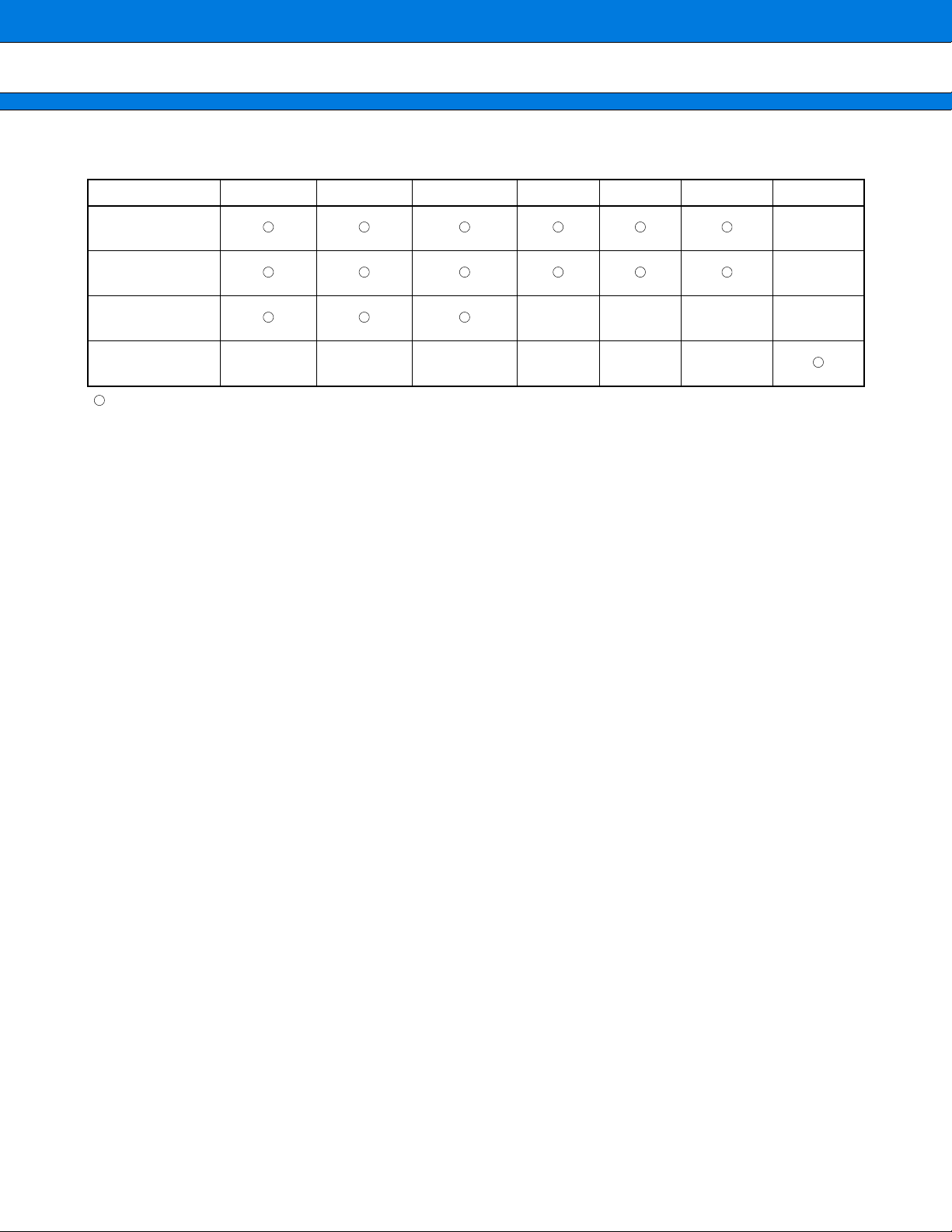
0 Normal mode 7 or 8 bits Asynchronous
1 Multi-processor mode 8 + 1
2 Clock synchronous mode 8 Synchronous None
: Not available
*1 : The “+1” represents the address/data (A/D) bit used for communication control.
*2 : Only 1 stop bit supported for receiving.
No. of Data Bits
No Parity With Parity
*1
Asynchronous
Synchronization No. of Stop Bits
1 or 2 bits
*2
•
UART interrupts and EI
Interrupt
UART1
receive interrupt
UART1
send interrupt
UART0
receive interrupt
UART0
send interrupt
: The UART has a function to halt EI
2
OS
Interrupt
No.
#37 (25
H) ICR13 0000BDH FFFF68H FFFF69H FFFF6AH
Interrupt Control
Register
Register
Name
Address Lower Upper Bank
Vector Table Address
#38 (26H) ICR13 0000BDH FFFF64H FFFF65H FFFF66H
#39 (27H) ICR14 0000BEH FFFF60H FFFF61H FFFF62H
#40 (28H) ICR14 0000BEH FFFF5CH FFFF5DH FFFF5EH
2
OS if a receive error is detected.
: Available when the interrupt shared with ICR13 or ICR14 is not used.
EI
2
OS
44
Page 45

MB90560/565 Series
(2) UART structure
The UART consists of the following 11 blocks:
• Clock selector • Mode registers (SMR0, SMR1)
• Receive control circuit • Control registers (SCR0, SCR1)
• Transmission control circuit • Status registers (SSR0, SSR1)
• Receive status evaluation circuit • Input data registers (SIDR0, SIDR1)
• Receive shift register • Output data registers (SODR0, SODR1)
• Transmission shift register
•
Block diagram
Control bus
Dedicated baud
rate generator
16-bit reload timer
Pin
P40/SCK0
<P62/SCK1>
Clock
selector
Receive
clock
Start bit
detection circuit
Receive
control circuit
Transmit clock
Transmission
start circuit
Transmission
control circuit
Receive
interrupt signal
H)*
#39 (27
<#37 (25H)*>
Transmit
interrupt signal
#40 (28
<#38 (26H)*>
H)*
Pin
P36/SIN0
<P60/SIN1>
Receive bit
counter
Receive parity
counter
Receive
shift register
Receive
SIDR0/SIDR1
Receive status
evaluation circuit
Internal data bus
MD1
MD0
CS2
SMR0/SMR1 SCR0/SCR1 SSR0/SSR1
CS1
CS0
SCKE
SOE
complete
Transmit bit
counter
Transmit parity
counter
Transmission
shift register
SODR0/SODR1
PEN
P
SBL
CL
A/D
REC
RXE
TXE
Pin
P37/SOT0
<P61/SOT1>
Transmission start
Receive error detection
signal for EI
(to CPU)
PE
ORE
FRE
RDRF
TDRE
BDS
RIE
TIE
2
OS
* : Interrupt number
45
Page 46

MB90560/565 Series
•
Clock selector
Selects the send/receive clock from either the dedicated baud rate generator, external input clock (clock input
to SCK0 or SCK1 pin) , or internal clock (clock supplied by 16-bit reload timer) .
•
Receive control circuit
The receive control circuit consists of a receive bit counter, start bit detection circuit, and receive parity counter .
The receive bit counter counts the received data bits and outputs a receive interrupt request when the required
number of data bits have been received. The star t bit detection circuit detects the star t bit on the serial input
signal. On detecting a start bit, the receive data is shifted to the input data register (SIDR0 or SIDR1) in
accordance with the specified transfer speed. The receive par ity counter calculates the parity of the received
data if parity is selected.
•
Transmission control circuit
The transmission control circuit consists of a transmission bit counter , transmission start circuit, and transmission
parity counter. The transmission bit counter counts the transmitted data bits and outputs a transmit interr upt
request when the required number of data bits have been sent. The tr ansmission start circuit starts transmission
when data is written to the output data register (SODR0 or SODR1) . The transmission parity counter generates
the parity bit for the transmitted data when parity is selected.
•
Receive shift register
The receive shift register captures the data input from the SIN0 or SIN1 pin by shifting one bit at a time then
transfers the received data to the input data register (SIDR0 or SIDR1) when reception completes.
•
Transmission shift register
The transmission data is transferred from the output data register (SODR0 or SODR1) to the tr ansmission shift
register and output from the SOT0 or SOT1 pin by shifting one bit at a time.
•
Mode register (SMR0, SMR1)
Set the operation mode, baud rate clock and serial clock input/output control, and enables output for the
serial data pin.
•
Control register (SCR0, SCR1)
Specifies whether to use parity, the type of parity, number of stop bits and data bits and the frame data format
for operation mode 1, to clear the receive error flag bit, and to enable or disable send and receive operation.
•
Status register (SSR0, SSR1)
Stores the send/receive and error status information, set the serial data transfer direction, and enab les or disables
the send and receive interrupt requests.
•
Input data register (SIDR0, SIDR1)
Stores the received data.
•
Output data register (SODR0, SODR1)
Set the transmission data. The data set in the output data register is converted to serial format and output.
46
Page 47

MB90560/565 Series
7. DTP/External Interrupt Circuit
(1) Overview of the DTP/external interrupt circuit
The DTP (Data Transfer Peripheral) /external interrupt circuit detects interrupt requests input to the external
interrupt input pins (INT7 to INT0) and outputs interrupt requests.
•
DTP/external interrupt circuit functions
The DTP/external interrupt function detects edge or level signals input to the e x ternal interrupt input pins (INT7
to INT0) and outputs interrupt requests.
The interrupt request is received by the CPU and, if the extended intelligent I/O ser vice (EI
2
EI
OS performs automatic data transfer (DTP function) then passes control to the interrupt handler routine on
completion. If EI
2
OS is disabled, control passes directly to the interrupt handler routine without performing
automatic data transfer (DTP function) .
•
Overview of the DTP/external interrupt circuit
External Interrupt DTP Function
Input pins 8 channels (P10/INT0 to P16/INT6, P63/INT7)
The level or edge to detect can be set independently for each pin in the detection lev-
Interrupt conditions
el setup register (ELVR) .
“L” level, “H” level, rising edge, or falling edge input
2
OS) is enabled,
Interrupt number #25 (19
Interrupt control
Interrupts can be enabled or disabled in the DTP/external interrupt enable register
(ENIR) .
H) to #28 (1CH)
Interrupt flag The DTP/external interrupt request register (ENRR) stores interrupt requests.
Processing selection Set EI
2
OS to disabled (ICR : ISE = 0) Set EI2OS to enabled (ICR : ISE = 1)
Jumps to interrupt handler routine after
Operation Jumps to interrupt handler routine
automatic data transfer by EI
2
OS com-
pletes.
ICR : Interrupt control register
•
DTP/external interrupt circuit interrupts and EI
Channel
Interrupt
No.
INT0/INT1 #25 (19
Interrupt Control Register Vector Table Address
Register Name Address Lower Upper Bank
H)
ICR07 0000B7
2
OS
FFFF98H FFFF99H FFFF9AH
H
INT2/INT3 #26 (1AH) FFFF94H FFFF95H FFFF96H
INT4/INT5 #27 (1BH)
ICR08 0000B8
FFFF90H FFFF91H FFFF92H
H
INT6/INT7 #28 (1CH) FFFF8CH FFFF8DH FFFF8EH
: Available when the interrupt shared with ICR07 or ICR08 is not used.
EI
2
OS
47
Page 48

MB90560/565 Series
(2) Structure of the DTP/external interrupt circuit
The DTP/external interrupt circuit consists of the following four blocks :
• DTP/interrupt detection circuit
• DTP/interrupt request register (EIRR)
• DTP/interrupt enable register (ENIR)
• Request level setting register (ELVR)
•
Block diagram
Request level setting register (ELVR)
LB7
LA7 LB6 LA6 LB5 LA5 LB4 LA4 LB3 LA3 LB2 LA2 LB1 LA1 LB0 LA0
22222222
Pin
P63/INT7 P10/INT0
Pin
P16/INT6 P11/INT1
Pin
P15/INT5
Pin
P14/INT4
DTP/interrupt
Internal data bus
request register
(EIRR)
DTP/interrupt
enable register
(ENIR)
Selector
Selector
ER7 ER6 ER5 ER4 ER3 ER2 ER1 ER0
EN7 EN6 EN5 EN4 EN3 EN2 EN1 EN0
DTP/external interrupt input detection circuit
Selector Selector
Selector Selector
Selector
Selector
Interrupt request signal
#25 (19H)*
#26 (1A
H)*
#27 (1B
H)*
#28 (1C
H)*
Pin
Pin
Pin
P12/INT2
Pin
P13/INT3
48
* : Interrupt number
Page 49

MB90560/565 Series
8. Delayed Interrupt Generation Module
• The delayed interrupt generation module is used to generate the task switching interrupt. Generation of this
hardware interrupt can be specified by software.
•
Delayed interrupt generation module functions
Function and Control
• Writing “1” to bit R0 of the delayed interrupt request generation/clear register
Interrupt trigger
Interrupt control • No enable/disable register is provided for this interrupt.
(DIRR : R0 = 1) generates an interrupt request.
• Writing “0” to bit R0 of the delayed interrupt request generation/clear register
(DIRR : R0 = 1) clears the interrupt request.
Interrupt flag
2
OS support
EI
•
Block diagram
Delayed interrupt request generation/
clear register (DIRR)
: Undefined
• Set in bit R0 of the delayed interrupt request generation/clear register
(DIRR : R0) .
• Not supported by the extended intelligent I/O service (EI
Internal data bus
R0
S
Interrupt request
latch
R
2
OS) .
Interrupt
request signal
49
Page 50

MB90560/565 Series
9. 8/10-Bit A/D Converter
•
Overview of the 8/10-bit A/D converter
• The 8/10-bit A/D converter uses RC successive appro ximation to convert analog input voltages to an 8-bit or
10-bit digital value.
• The input signals can be selected from the eight analog input pin channels.
•
8/10-bit A/D converter functions
The minimum conversion time is 6.13 µs (for a 16 MHz machine clock, including sampling
A/D conversion time
Conversion method RC successive approximation with sample & hold circuit
Resolution 8-bit or 10-bit, selectable
Analog input pins Eight analog input pin channels are available. The input pin can be selected by the program.
Interrupts
time) .
The minimum sampling time is 2.0 µs (for a 16 MHz machine clock)
An interrupt request can be generated and EI
2
OS invoked when A/D conversion completes.
The conversion data protection function operates when A/D conversion is performed with
the interrupt enabled.
A/D conversion
start trigger
2
EI
OS support Supported by the extended intelligent I/O service (EI2OS) .
•
8/10-bit A/D converter conversion modes
The conversion start trigger can be set from the following options : software, output of 16bit reload timer 1 (rising edge) , or zero detection edge from 16-bit freerun timer.
Conversion Mode Single Conversion Mode Operation Scan Conversion Mode Operation
Single-shot conversion mode 1
Single-shot conversion mode 2
Continuous conversion mode
Performs one conversion for the specified channel (1 channel) then halts.
Performs repeated conversions for the
specified channel (1 channel) .
Performs one conversion for the spec-
Incremental conversion mode
ified channel (1 channel) then halts
and waits for the next activation.
•
8/10-bit A/D converter interrupts and EI
2
OS
Sequentially performs one conversion
for multiple channels (up to 8 channels
can be set) , then halts.
Performs repeated conversions for the
specified channels (up to 8 channels
can be set) .
Sequentially performs one conversion
for multiple channels (up to 8 channels
can be set) , then halts and waits for
the next activation.
Interrupt Control Register Vector Table Address
Interrupt No.
Register Name Address Lower Upper Bank
#11 (0B
H) ICR00 0000B0H FFFFD0H FFFFD1H FFFFD2H
: Available
EI
2
OS
50
Page 51
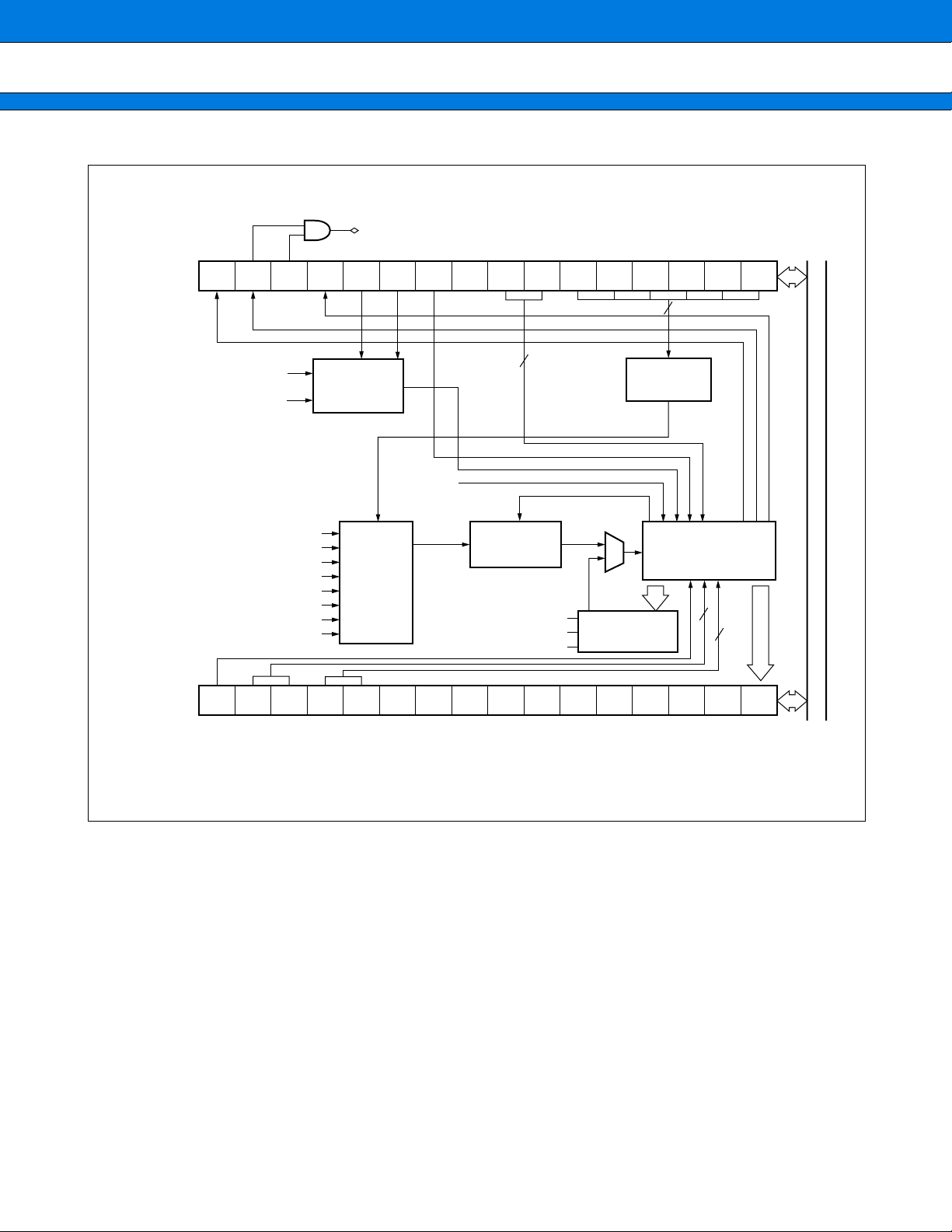
•
Block diagram
MB90560/565 Series
A/D control status register
(ADCS0, ADCS1)
BUSY
INT INTE
16-bit reload timer 1 output
16-bit freerun timer zero-detect
A/D data register
(ADCR0, ADCS1)
P57/AN7
P56/AN6
P55/AN5
P54/AN4
P53/AN3
P52/AN2
P51/AN1
P50/AN0
Interrupt request signal #11 (0B
PAUS STS1
Clock selector
Analog
channel
selector
STS0
STRT
Rese-
rved
φ
MD1
MD0
2
Sample &
hold circuit
AVR
AV
AVSS
H) *
ANS2 ANS1 ANS0 ANE2
Comparator
CC
D/A converter
ANE1 ANE0
6
Decoder
Internal data bus
Control circuit
2
2
S10
ST1
φ : Machine clock
* : Interrupt number
ST0 CT1 CT0
D7 D6 D4 D3 D2
D8 D5
D9
D1
D0
51
Page 52

MB90560/565 Series
10. ROM Mirror Function Selection Module
• The ROM mirror function selection module enables ROM data in FF bank to be read by accessing 00 bank.
•
ROM mirror function selection module functions
Function
Mirror setting address
• Data in FFFFFF
in 00 bank.
H to FF4000H in FF bank can be read from 00FFFFH to 004000H
Interrupts • None
2
EI
OS support
•
Relationship between addresses in the ROM mirror function
FEFFFFH
FFFFFFH
•
Block diagram
• Not supported by the extended intelligent I/O service (EI
FE0000H
FE8000H
FF0000H
FF4000H
FF bank
FF8000H
Mirrored ROM
data area
ROM area in MB90562/A and MB90F562/B
ROM area in MB90561/A
ROM area in MB90568 and MB90F568
ROM area in MB90567
2
OS) .
52
Address
Internal data bus
Data
FF bank
ROM mirror function selection register (ROMM)
Address space
00 bank
ROM
MI
Page 53

MB90560/565 Series
11. Low Power Consumption (Standby) Modes
• The power consumption of F2MC-16LX devices can be reduced by various settings that control the operating
clock selection.
•
Functions of each CPU operation mode
CPU Operation
Clock
Operation
Mode
Normal Run
Function
The CPU and peripheral functions operate using the oscillation clock (HCLK)
multiplied by the PLL circuit.
PLL clock
Main clock
CPU intermittent
operation
Sleep
Pseudo-clock
Stop The oscillation clock is stopped and the CPU and peripherals halt operation.
Normal Run
Sleep
Stop The oscillation clock is stopped and the CPU and peripherals halt operation.
Normal Run
The peripheral functions only operate using the oscillation clock (HCLK) multiplied by the PLL circuit.
The timebase timer only operates using the oscillation clock (HCLK) multiplied by the PLL circuit.
The CPU and peripheral functions operate using the oscillation clock (HCLK)
divided into 2.
The peripheral functions only operate using the oscillation clock (HCLK) divided into 2.
The oscillation clock (HCLK) divided into 2 operates intermittently for fixed
time intervals.
53
Page 54
MB90560/565 Series
12. 512 Kbit Flash Memory
• This section describes the flash memory on the MB90F562/B and does not apply to evaluation and mask ROM
versions.
• The flash memory is located in bank FF in the CPU memory map.
•
Flash memory functions
Function
Memory size • 512 Kbit (64 KBytes)
Memory configuration • 64 KWords × 8 bits or 32 KWords × 16 bits
Sector configuration • 16 KBytes + 8 KBytes + 8 KBytes + 32 KBytes
Sector protect function • Selectable for each sector
*
Programming algorithm
Operation commands
• Automatic programming algorithm (Embedded Algorithm
MBM29F400TA)
• Compatible with JEDEC standard commands
• Includes an erase pause and restart function
• Write/erase completion detection by data polling or toggle bit
• Erasing by sector available (sectors can be combined in any combination)
: Equivalent to
No. of write/erase cycles • Min. 10,000 guaranteed
• Can be written and erased using a parallel writer
(Ando Denki AF9704, AF9705, AF9706, AF9708, and AF9709)
Memory write/erase method
• Can be written and erased using a dedicated serial writer
(Yokoga wa Digital Computer Corporation AF200, AF210, AF120, and AF110)
• Can be written and erased by the program
Interrupts • Write and erase completion interrupts
2
EI
OS support
• Not supported by the extended intelligent I/O service (EI
* : Embedded Algorithm is a trademark of Advanced Micro Devices.
•
Sector configuration of flash memory
Flash memory CPU address Writer address*
FF0000
SA1 (32 Kbyte)
SA2 (8 Kbyte)
SA3 (8 Kbyte)
SA4 (16 Kbyte)
H
FF7FFFH
FF8000H
FF9FFFH
FFA000H
FFBFFFH
FFC000H
FEFFFFH
70000H
77FFFH
78000H
79FFFH
7A000H
7BFFFH
7C000H
7FFFFH
2
OS) .
* : The writer address is the address to be used instead of the CPU address when writing data from a parallel
flash memory writer. Use the writer address when programming or erasing with a general-purpose parallel
writer.
54
Page 55

MB90560/565 Series
13. 1 Mbit Flash Memory
• This section describes the flash memory on the MB90F568 and does not apply to evaluation and mask ROM
versions.
• The flash memory is located in banks FE to FF in the CPU memory map.
•
Flash memory functions
Function
Memory size • 1 Mbit (128 KBytes)
Memory configuration • 128 KWords × 8 bits or 64 KWords × 16 bits
Sector configuration • 16 KBytes + 8 KBytes + 8 KBytes + 32 KBytes + 64 KBytes
Sector protect function • Selectable for each sector
Programming algorithm
• Automatic programming algorithm (Embedded Algorithm* : Equivalent to
MBM29F400TA)
• Compatible with JEDEC standard commands
Operation commands
• Includes an erase pause and restart function
• Write/erase completion detection by data polling or toggle bit
• Erasing by sector available (sectors can be combined in any combination)
No. of write/erase cycles • Min. 10,000 guaranteed
• Can be written and erased using a parallel writer
(Ando Denki AF9704, AF9705, AF9706, AF9708, and AF9709)
Memory write/erase method
• Can be written and erased using a dedicated serial writer
(Yokoga wa Digital Computer Corporation AF200, AF210, AF120, and AF110)
• Can be written and erased by the program
Interrupts • Write and erase completion interrupts
EI2OS support
• Not supported by the extended intelligent I/O service (EI
* : Embedded Algorithm is a trademark of Advanced Micro Devices.
•
Sector configuration of flash memory
Flash memory CPU address Writer address*
FE0000
SA0 (64 Kbyte)
SA1 (32 Kbyte)
SA2 (8 Kbyte)
SA3 (8 Kbyte)
SA4 (16 Kbyte)
H
FEFFFH
FF0000H
FF7FFFH
FF8000H
FF9FFFH
FFA000H
FFBFFFH
FFC000H
FEFFFFH
60000H
6FFFFH
70000H
77FFFH
78000H
79FFFH
7A000H
7BFFFH
7C000H
7FFFFH
2
OS) .
* : The writer address is the address to be used instead of the CPU address when writing data from a parallel
flash memory writer. Use the writer address when programming or erasing with a general-purpose parallel
writer.
55
Page 56

MB90560/565 Series
• Standard configuration for Fujitsu standard serial on-board programming
Fujitsu standard serial on-board programming uses a flash microcontroller writer from Yokogawa Digital Computer Corporation (AF220, AF210, AF120, or AF210) .
Host interface cable (AZ201)
Flash
RS232C
microcontroller
writer
+
memory card
General-purpose cable (AZ221)
Clock synchronous
serial
Can operate standalone
MB90F562/F562B/F568
user system
Note : Contact Yokogawa Digital Computer Corporation for details of the functions and operation of the flash
microcontroller writer (AF220, AF210, AF120, or AF110) , standard connection cable (AZ221) , and connectors.
•
Pins used for Fujitsu standard serial on-board programming
Symbol Pin name Function
MD2,
MD1, MD0
Mode input pins
Setting MD2 = 1, MD1 = 1, and MD0 = 0 selects serial programming
mode.
As flash memory serial programming mode uses the PLL clock with the
multiplier set to 1 as the internal CPU operation clock, the internal op-
X0, X1 Oscillation input pin
eration clock frequency is the same as the oscillation clock frequency.
Accordingly, the frequency that can be input to the high speed oscillation input pin when performing serial programming is between 1 MHz
and 16 MHz.
P00, P01
RST
SIN1 Serial data input pin
SOT1 Serial data output pin
SCK0 Serial clock input pin
C
Write program activation
pins
Input P00 = “L” level and P01 = “H” level.
Reset input pin
Uses UART0 and UART1 in clock synchronous mode. In programming
mode, the pins used by UART0 in clock synchronous mode are SIN1,
SOT1, and SCK0.
Capacitor/power supply input pin
Capacitor pin for power supply stabilization. Connect an external ce-
ramic capacitor of approx. 0.1 µF.
If the user system provides the programming voltage (MB90F562 :
V
CC Power supply input pins
5 V ± 10%, MB90F568 : 3 V ± 10%) , these do not need to be connected
to the flash microcontroller writer.
VSS GND pin Connect to common GND with the flash microcontroller writer.
56
Page 57

MB90560/565 Series
The control circuit shown in the figure is required when the P00, P01, SIN1, SOT1, and SCK0 pins are used on
the user system. Use the /TICS signal from the flash microcontroller writer to disconnect the user circuit during
serial on-board programming.
AF220/AF210/AF120/AF110
write control pin
10 kΩ
AF220/AF210/AF120/AF110
/TICS pin
User
MB90F562/F562B/F568
write control pin
Control circuit
Use the formula below to calculate the serial clock frequency able to be input to the MB90F562/F562B/F568.
Set up the flash microcontroller writer to use a serial clock input frequency that is permitted for the oscillation
clock frequency you are using.
Permitted input serial clock frequency = 0.125 × oscillation clock frequency
•
Maximum serial clock frequency
Oscillation
Clock
Frequency
Maximum Serial Clock
Frequency that can be Input
to Microcontroller
Maximum Serial Clock
Frequency that can be Set on
the AF220/AF210/AF120/AF110
Maximum Serial Clock
Frequency that can be Set on
the AF200
4 MHz 500 kHz 500 kHz 500 kHz
8 MHz 1 MHz 850 kHz 500 kHz
16 MHz 2 MHz 1.25 MHz 500 kHz
•
System configuration of flash microcontroller writer (AF220/AF210/AF120/AF110) (Supplier : Yokogawa Digital Computer Corporation)
Model Function
AF200/AC4P Internal Ethernet interface model /100 V to 220 V power adapter
AF210/AC4P Standard model /100 V to 220 V power adapter
Unit
AF120/AC4P Single key, Internal Ethernet interface model /100 V to 220 V power adapter
AF110/AC4P Single key model /100 V to 220 V power adapter
AZ221 Special RS232C cable for connecting writer to PC/AT
AZ210 Standard target probe (a) Length : 1 m
2
FF201 Control module for Fujitsu F
MC-16LX flash microcontrollers
AZ290 Remote controller
AZ264
Power supply regulator (MB90F568 : Required to supply 3 V versions from the flash
microcontroller writer.)
/P2 2 MB PC card (option) Supports FLASH memory sizes up to 128 KB
/P4 4 MB PC card (option) Supports FLASH memory sizes up to 512 KB
Contact : Yokogawa Digital Computer Corporation Tel : 042-333-6224
Note : The AF200 flash microcontroller writer is an obsolete model but can still be used with the FF201 control
module.
57
Page 58
MB90560/565 Series
ELECTRICAL CHARACTERISTICS (MB90560 SERIES)
■
1. Absolute Maximum Ratings
Parameter Symbol
CC VSS − 0.3 VSS + 6.0 V
V
Power supply voltage
AVCC VSS − 0.3 VSS + 6.0 V VCC ≥ AVCC
AVR VSS − 0.3 VSS + 6.0 V AVCC ≥ AVR ≥ 0 V
Input voltage VI VSS − 0.3 VSS + 6.0 V *2
Output voltage VO VSS − 0.3 VSS + 6.0 V *2
OL1 15 mA *3, *4
“L” level maximum output
current
I
I
OL2 20 mA *3, *5
IOLAV1 4mA
“L” level average output
current
IOLAV2 12 mA
Rating
Unit Remarks
Min. Max.
(VSS = AVSS = 0.0 V)
*1
*1
Average value
(operating current × operating ratio)
Average value
(operating current × operating ratio)
*4
*5
“L” level total maximum
output current
“L” level total average
output current
“H” level maximum output
current
“H” level average output
current
“H” level total maximum
output current
“H” level total average
output current
ΣIOL 100 mA
ΣIOLAV 50 mA
I
OH −15 mA *3
I
OHAV −4mA
ΣI
OH −100 mA
ΣIOHAV −50 mA
Power consumption Pd 300 mW
Operating temperature T
A −40 +85 °C
Storage temperature Tstg −55 +150 °C
*1 : AV
CC and AVR must not exceed VCC. Also, AVR must not exceed AVCC.
*2 : V
I and VO must not exceed VCC + 0.3 V.
*3 : The maximum output current is the peak value for a single pin.
*4 : Pins other than P30/RTO0 to P35/RTO5
Average value
(operating current × operating ratio)
Average value
(operating current × operating ratio)
Average value
(operating current × operating ratio)
*5 : P30/RTO0 to P35/RTO5 pins
WARNING: Semiconductor devices can be permanently damaged by application of stress (voltage, current,
temperature, etc.) in excess of absolute maximum ratings. Do not exceed these ratings.
58
Page 59

2. Recommended Operating Conditions
Value
Parameter Symbol
Min. Max.
MB90560/565 Series
(VSS = AVSS = 0.0 V)
Unit Remarks
Power supply voltage
V
V
VIH 0.7 VCC VCC + 0.3 V CMOS input pin
Input “H” voltage
V
V
Input “L” voltage
V
V
Smoothing capacitor C
Operating
temperature
• C pin diagram
CC
3.0 5.5 V
Normal operation (MB90562, 562A, 561,
561A, and V560)
4.5 5.5 V Normal operation (MB90F562 and F562B)
CC 3.0 5.5 V Maintaining state in stop mode
IHS 0.8 VCC VCC + 0.3 V CMOS hysteresis input pin
IHM VCC − 0.3 VCC + 0.3 V MD input pin
VIL VSS − 0.3 0.3 VCC V CMOS input pin
ILS VSS − 0.3 0.2 VCC V CMOS hysteresis input pin
ILM VSS − 0.3 VSS + 0.3 V MD input pin
Use a ceramic capacitor or other capacitor
with equivalent frequency characteristics.
S 0.1 1.0 µF
T
A −40 +85 °C
The capacitance of the smoothing capacitor
connected to the V
than C
S.
CC pin must be greater
C
C
S
WARNING: The recommended operating conditions are required in order to ensure the nor mal operation of the
semiconductor device. All of the device’s electrical characteristics are warranted when the device is
operated within these ranges.
Always use semiconductor devices within their recommended operating condition ranges. Operation
outside these ranges may adversely affect reliability and could result in device failure.
No warranty is made with respect to uses, operating conditions, or combinations not represented on
the data sheet. Users considering application outside the listed conditions are advised to contact their
FUJITSU representatives beforehand.
59
Page 60

MB90560/565 Series
3. DC Characteristics
Parameter
Sym-
bol
Pin Name Condition
(TA = −40 °C to +85 °C, VCC = 5.0 V ±10%, VSS = AVSS = 0.0 V)
Value
Unit Remarks
Min. Typ. Max.
Output “H”
voltage
Output “L”
voltage
Input leak
current
Power supply
current
*
OH
V
All output
pins
VCC = 4.5 V
I
OH = −2.0 mA
VCC − 0.5 V
Pins other
OL1
V
than P30/
RTO0 to
V
CC = 4.5 V
I
OL1 = 2.0 mA
0.4 V
P35/RTO5
V
OL2
IIL
P30/RTO0
to P35/
RTO5
All output
pins
VCC = 4.5 V
I
OL2 = 12.0 mA
VCC = 5.5 V
V
SS < VI < VCC
For VCC = 5 V,
0.8 V
−5 5 µA
50 80 mA
internal frequency = 16 MHz,
ICC
normal operation
CC = 5 V,
For V
40 50 mA MB90F562/B
55 85 mA
internal frequency = 16 MHz,
VCC
A/D operation in progress
45 55 mA MB90F562/B
Flash write or erase 45 60 mA MB90F562/B
For VCC = 5 V,
I
CCS
internal frequency = 16 MHz,
15 20 mA
sleep mode
ICCH Stop mode, TA = 25 °C 520µA
MB90562/A,
MB90561/A
MB90562/A,
MB90561/A
MB90562/A,
MB90561/A
MB90F562/B
*
Other than
AV
Input
capacitance
C
IN
CC,
AV
SS, C,
V
CC, and
V
SS
10 80 pF
P00 to P07
Pull-up
resistor
R
UP
P10 to P17
RST
, MD0,
15 30 100 kΩ
MD1
Pull-down
resistor
R
DOWN MD2 15 30 100 kΩ
* : Value when low power mode bits (LPM0, 1) is set to “01” with an internal operating frequency of 4 MHz.
Note : Current values are provisional and are subject to change without notice to allow for improvements to the
characteristics. The power supply current is measured with an external clock.
60
Page 61
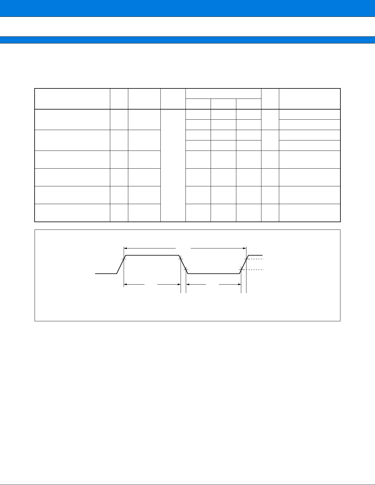
4. AC Characteristics
(1) Clock Timings
Parameter
Sym
bol
Pin Name
MB90560/565 Series
(T
A = −40 °C to +85 °C, VCC = 5.0 V ±10%, VSS = AVSS = 0.0 V)
Condi-
tion
Min. Typ. Max.
Value
Unit Remarks
Clock frequency f
Clock cycle time t
Input clock pulse width
Input clock rise/fall time
Internal operating clock
frequency
Internal operating clock
cycle time
•
X0 and X1 clock timing
X0
3 16
C X0, X1
MHz
1 16 Without a PLL circuit
62.5 333
HCYL X0, X1
62.5 1000 Without a PLL circuit
P
WH
PWL
tcr
tcf
f
CP 1.5 16 MHz
t
CP 62.5 333 ns
X0 10 ns
X0 5ns
tHCYL
0.8 VCC
0.2 VCC
PWH PWL
With a PLL circuit
With a PLL circuit
ns
Recommended duty
ratio = 30% to 70%
When using an
external clock
When using a main
clock
When using a main
clock
tcf
tcr
61
Page 62
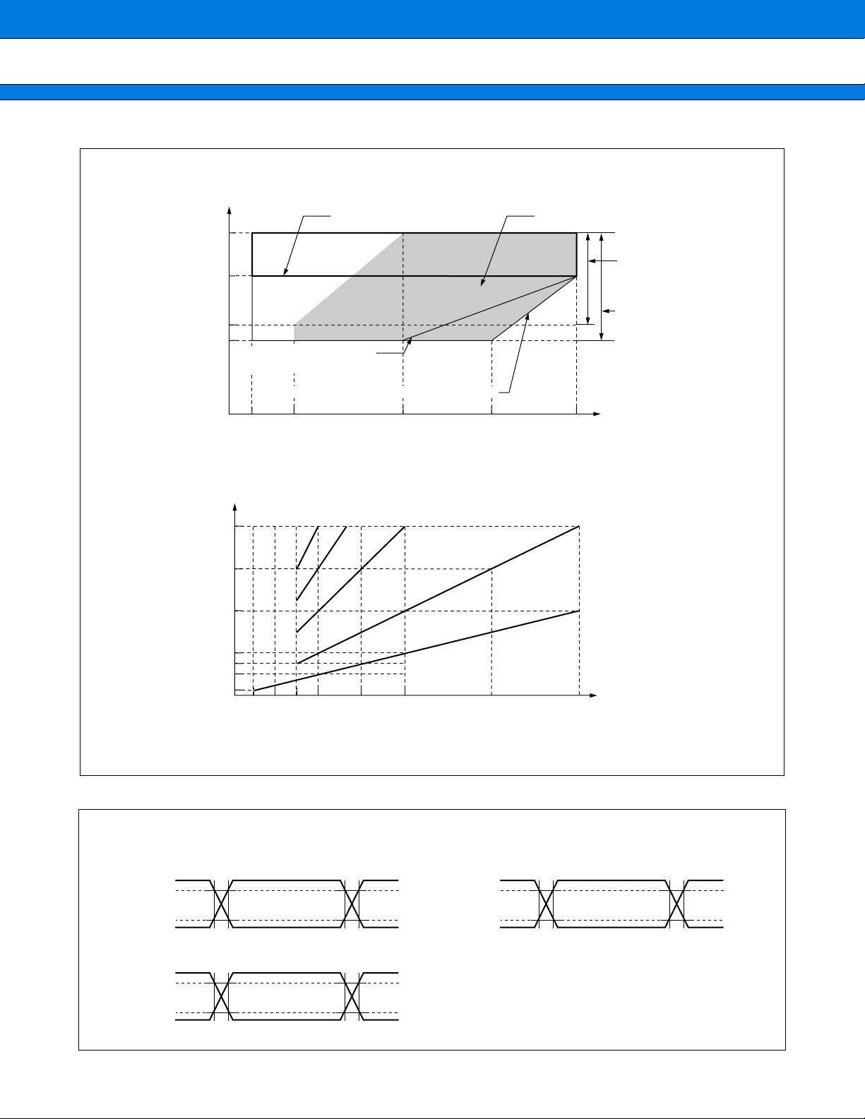
MB90560/565 Series
•
PLL guaranteed operation range
Relationship between internal operating clock frequency and power supply voltage
Guaranteed operation range
5.5
4.5
3.3
3.0
Guaranteed operation range
for MB90561/A and MB90562/A
Supply Voltage VCC (V)
Guaranteed operation range for MB90V560
13 8 12 16
for MB90F562/B
PLL guaranteed operation range
PLL guaranteed
operation range
A/D converter guaranteed
operation range
Internal Clock fCP (MHz)
Relationship between oscillation frequency and internal operating clock frequency
16
12
8
4
3
Internal Clock fCP (MHz)
2
0.5
1234 6 8
×4 ×3 ×2 ×1
12 16
Source Oscillation Clock fC (MHz)
The AC ratings are specified for the following measurement reference voltages.
•
Input signal waveform
Hysteresis input pin
0.8 VCC
•
Output signal waveform
Output pin
2.4 V
No multiplier
62
0.2 VCC
Pins other than hysteresis input or MD input pins
0.7 V
CC
0.3 VCC
0.8 V
Page 63

(2)Reset
(T
A = −40 °C to +85 °C, VCC = 5.0 V ±10%, VSS = AVSS = 0.0 V)
Parameter Symbol Pin Name Condition
MB90560/565 Series
Value
Unit Remarks
Min. Max.
In normal
operation
Reset input time t
RSTH RST
16 t
CP ns
Oscillator oscillation
time* + 16 t
CP
ms In stop mode
*: Oscillator oscillation time is the time to reach 90% amplitude. For a crystal oscillator, this is a few to several
dozen ms; for a F AR/ceramic oscillator, this is se veral hundred µs to a f ew ms, and for an external clock this is 0 ms .
• In normal operation
tRSTL
RST
0.2 VCC
0.2 VCC
• In stop mode
tRSTL
RST
0.2Vcc
0.2Vcc
X0
Internal
operation
clock
Internal
reset
90 % of
amplitude
Oscillator
oscillation time
16 tcp
Oscillator stabilization wait time
Execution of the instruction
63
Page 64

MB90560/565 Series
(3) Power-On Reset
Parameter Symbol Pin Name
(T
A = −40 °C to +85 °C, VCC = 5.0 V ±10%, VSS = AVSS = 0.0 V)
Condi-
tion
Value
Unit Remarks
Min. Max.
Power supply rise time t
R VCC
0.05 30 ms
Power supply cutoff time t
* : V
CC must be less than 0.2 V before power-on.
OFF VCC 4 ms For repeated operation
Notes : • The above rating values are for generating a power-on reset.
• Some internal registers are only initialized by a power-on reset. Always apply the power supply in
accordance with the above ratings if you wish to initialize these registers.
tR
VCC
2.7 V
0.2 V0.2 V
t
OFF
Sudden changes in the power supply voltage may cause a power-on reset.
The recommended practice if you wish to change the power supply voltage while the device is
operating is to raise the voltage smoothly as shown below. Also, changes to the supply voltage
should be performed when the PLL clock is not in use. The PLL clock may be used, however, if
the rate of voltage change is 1 V/s or less.
VCC
3.0 V
V
SS
Maintain RAM data
0.2 V
Recommended rate of voltage
rise is 50 mV/ms or less.
64
Page 65

(4) UART0, UART1, and I/O Expansion Serial Timings
(T
A = −40 °C to +85 °C, VCC = 5.0 V ±10%, VSS = AVSS = 0.0 V)
Parameter Symbol Pin Name Condition
MB90560/565 Series
Value
Unit Remarks
Min. Max.
Serial clock cycle time t
SCK ↓ → SOT delay
time
Valid SIN → SCK ↑ t
SCK ↑ → valid
SIN hold time
Serial clock “H” pulse
width
Serial clock “L” pulse
width
SCK ↓ → SOT delay
time
Valid SIN → SCK ↑ t
SCK ↑ → valid
SIN hold time
SCYC SCK0, SCK1
t
SLOV
IVSH
t
SHIX
t
SHSL SCK0, SCK1
SCK0, SCK1
SOT0, SOT1
SCK0, SCK1
SIN0, SIN1
SCK0, SCK1
SIN0, SIN1
Internal shift clock
mode, output pin load is
CL = 80 pF + 1 TTL
tSLSH SCK0, SCK1 4 tCP ns
External shift clock
mode, output pin load is
CL = 80 pF + 1 TTL
t
SLOV
IVSH
t
SHIX
SCK0, SCK1
SOT0, SOT1
SCK0, SCK1
SIN0, SIN1
SCK0, SCK1
SIN0, SIN1
Notes : • These are the AC ratings for CLK synchronous mode.
• C
L is the load capacitor connected to the pin for testing.
• t
CP is the machine cycle period (unit = ns)
8 tCP ns
−80 80 ns
100 ns
60 ns
4 tCP ns
150 ns
60 ns
60 ns
65
Page 66
MB90560/565 Series
•
Internal shift clock mode
SCK
0.8 V 0.8 V
tSLOV
SOT
SIN
•
External shift clock mode
SCK
0.2 VCC 0.2 VCC
tSCYC
2.4 V
2.4 V
0.8 V
tIVSH tSHIX
0.8 V
CC
0.2 VCC
tSLSH tSHSL
0.8 VCC 0.8 VCC
0.8 VCC
0.2 VCC
SOT
SIN
tSLOV
2.4 V
0.8 V
tIVSH tSHIX
0.8 V
CC
0.2 VCC
0.8 VCC
0.2 VCC
66
Page 67

(5) Timer Input Timings
Parameter Symbol Pin Name
MB90560/565 Series
(T
A = −40 °C to +85 °C, VCC = 5.0 V ±10%, VSS = AVSS = 0.0 V)
Condi-
tion
Value
Unit Remarks
Min. Max.
Input pulse width t
TIWH, tTIWL FRCK, IN0, IN1, TIN0, TIN1 4 tCP ns
0.8 VCC 0.8 VCC
(6) Timer Output Timings
Parameter Symbol Pin Name
CLK ↑ → T
OUT change time tTO
CLK
0.2 VCC 0.2 VCC
tTIWH tTIWL
(T
A = −40 °C to +85 °C, VCC = 5.0 V ±10%, VSS = AVSS = 0.0 V)
RTO0 to RTO5,
PPG0 to PPG5, TO0 to TO1
2.4 V
t
TO
Condi-
tion
Value
Min. Max.
30 ns
Unit Remarks
T
OUT
2.4 V
0.8 V
(7) Trigger Input Timings
(T
A = −40 °C to +85 °C, VCC = 5.0 V ±10%, VSS = AVSS = 0.0 V)
Parameter Symbol Pin Name Condition
Input pulse width t
TRGL INT0 to INT7, IN0 to IN3
0.8 VCC 0.8 VCC
0.2 VCC 0.2 VCC
tTRGH tTRGL
Value
Unit Remarks
Min. Max.
5 t
CP ns
In normal
operation
1 µs In stop mode
67
Page 68

MB90560/565 Series
5. Electrical Characteristics for the A/D Converter
(TA = −40 °C to +85 °C, 3.0 V ≤ AVR, VCC = AVCC = 5.0 V ±10%, VSS = AVSS = 0.0 V)
Parameter Symbol Pin Name
Min. Typ. Max.
Resolution 10 bit
Total error ±5.0 LSB
Non-linearity error ±2.5 LSB
Differential linearity error ±1.9 LSB
Value
Unit Remarks
Zero transition voltage V
OT AN0 to AN7
AVSS
−3.5 LSB
+0.5
SS
AV
+4.5 LSB
mV
1 LSB = AVRH/1024
Full-scale transition
voltage
FST AN0 to AN7
V
AVR
−6.5 LSB
AVR
−1.5 LSB
AVR
+1.5 LSB
mV
Conversion time 176 tCP ns
Sampling time 64 t
Analog port input
current
I
AIN AN0 to AN7 10 µA
CP ns
Analog input voltage VAIN AN0 to AN7 0 AVR V
Reference voltage AVR 2.7 AV
A AVCC 5 mA
I
CC V
Power supply current
IAH AVCC 5 µA*
I
Reference voltage
supply current
Variation between
channels
* : Current when A/D converter is not used and CPU is in stop mode (V
R AVR 400 µA
I
RH AVR 5 µA*
AN0 to AN7 4LSB
CC = AVCC = AVR = 5.0 V)
Notes : • The L reference v oltage is fixed to AVSS. The relative error increases as AVR becomes smaller.
• Ensure that the output impedance of the e xternal circuit connected to the analog input meets the following
condition :
Output impedance of external circuit ≤ 10 kΩ (Sampling Time = 4.0 µs)
• If the output impedance of the external circuit is too high, the analog voltage sampling time may be too short.
• Equivalent circuit of analog input circuit
Analog input
Note : The values listed are an indication only.
68
MB90561/A, MB90562/A
R
ON = 2.2 kΩ approx.
C = 45 pF approx.
MB90F562
R
ON = 3.2 kΩ approx.
C = 30 pF approx.
MB90F562/B
R
ON = 2.6 kΩ approx.
C = 28 pF approx.
CRON
Comparator
Page 69
6. Flash Memory Erase and Programming Performance
MB90560/565 Series
Parameter Condition
Sector erase time
T
Chip erase time 5 s
Word (16 bit width)
programming time
Erase/Program cycle 10,000 cycle
Data holding time 100,000 h
A = + 25 °C
Vcc = 5.0 V
Min Typ Max
115s
16 3,600 µs Excludes system-level overhead
Value
Units Remarks
Excludes 00H programming prior
erasure
Excludes 00H programming prior
erasure
69
Page 70

MB90560/565 Series
ELECTRICAL CHARACTERISTICS (MB90565 SERIES)
■
1. Absolute Maximum Ratings
Parameter Symbol
CC VSS − 0.3 VSS + 4.0 V
V
Power supply voltage
AVCC VSS − 0.3 VSS + 4.0 V VCC ≥ AVCC
AVR VSS − 0.3 VSS + 4.0 V AVCC ≥ AVR ≥ 0 V
Input voltage VI VSS − 0.3 VSS + 4.0 V *2
Output voltage VO VSS − 0.3 VSS + 4.0 V *2
Rating
Unit Remarks
Min. Max.
(VSS = AVSS = 0.0 V)
*1
*1
“L” level maximum output
current
“L” level average output
current
“L” level total maximum
output current
“L” level total average
output current
“H” level maximum output
current
“H” level average output
current
“H” level total maximum
output current
“H” level total average
output current
I
OL 15 mA *3
I
OLAV 4mA
ΣIOL 100 mA
ΣI
OLAV 50 mA
I
OH −15 mA *3
I
OHAV −4mA
ΣIOH −100 mA
ΣI
OHAV −50 mA
Power consumption Pd 300 mW
Operating temperature T
A −40 +85 °C
Storage temperature Tstg −55 +150 °C
*1 : AV
CC and AVR must not exceed VCC. Also, AVR must not exceed AVCC.
Average value
(operating current × operating ratio)
Average value
(operating current × operating ratio)
Average value
(operating current × operating ratio)
Average value
(operating current × operating ratio)
*2 : V
I and VO must not exceed VCC + 0.3 V.
*3 : The maximum output current is the peak value for a single pin.
WARNING: Semiconductor devices can be permanently damaged by application of stress (voltage, current,
temperature, etc.) in excess of absolute maximum ratings. Do not exceed these ratings.
70
Page 71

2. Recommended Operating Conditions
Value
Parameter Symbol
Min. Max.
3.0 3.6 V Normal operation (MB90V560)
MB90560/565 Series
(VSS = AVSS = 0.0 V)
Unit Remarks
Power supply voltage V
CC
2.7 3.6 V
Normal operation (MB90F568, MB90567
and MB90568)
2.5 3.6 V Maintaining state in stop mode
V
IH 0.7 VCC VCC + 0.3 V CMOS input pin
Input “H” voltage
V
IHS 0.8 VCC VCC + 0.3 V CMOS hysteresis input pin
V
IHM VCC − 0.3 VCC + 0.3 V MD input pin
VIL VSS − 0.3 0.3 VCC V CMOS input pin
Input “L” voltage
V
ILS VSS − 0.3 0.2 VCC V CMOS hysteresis input pin
V
ILM VSS − 0.3 VSS + 0.3 V MD input pin
Operating temperature TA −40 +85 °C
WARNING: The recommended operating conditions are required in order to ensure the nor mal operation of the
semiconductor device. All of the device’s electrical characteristics are warranted when the device is
operated within these ranges.
Always use semiconductor devices within their recommended operating condition ranges. Operation
outside these ranges may adversely affect reliability and could result in device failure.
No warranty is made with respect to uses, operating conditions, or combinations not represented on
the data sheet. Users considering application outside the listed conditions are advised to contact their
FUJITSU representatives beforehand.
71
Page 72

MB90560/565 Series
3. DC Characteristics
Parameter
Sym
Pin Name Condition
bol
(TA = −40 °C to +85 °C, VCC = 2.7 V to 3.6 V, VSS = AVSS = 0.0 V)
Value
Unit Remarks
Min. Typ. Max.
Output “H”
voltage
Output “L”
voltage
Input leak
current
Power
supply
current*
V
OH
V
OL
I
IL
I
CC
All output
pins
All output
pins
All output
pins
VCC
VCC = 3.0 V
I
OH = −2.0 mA
VCC = 3.0 V
I
OL = 2.0 mA
VCC = 3.0 V
V
SS < VI < VCC
For VCC = 3.3 V,
internal frequency = 8 MHz,
normal operation
For V
CC = 3.3 V,
internal frequency = 16 MHz,
normal operation
For V
CC = 3.3 V,
internal frequency = 8 MHz,
A/D operation in progress
For V
CC = 3.3 V,
internal frequency = 16 MHz,
A/D operation in progress
For V
CC = 3.3 V,
internal frequency = 8 MHz,
normal operation
For V
CC = 3.3 V,
internal frequency = 16 MHz,
normal operation
VCC − 0.5 VCC − 0.3 V
0.2 0.4 V
−5 −15µA
14 22 mA MB90567/568
27 40 mA MB90567/568
18 27 mA MB90567/568
32 45 mA MB90567/568
18 28 mA MB90F568
36 45 mA MB90F568
For V
CC = 3.3 V,
internal frequency = 8 MHz,
23 33 mA MB90F568
A/D operation in progress
For V
CC = 3.3 V,
internal frequency = 16 MHz,
41 50 mA MB90F568
A/D operation in progress
Flash write or erase 40 50 mA MB90F568
I
CCS
For VCC = 3.3 V,
internal frequency = 8 MHz,
sleep mode
For VCC = 3.3 V,
internal frequency = 16 MHz,
sleep mode
610mA
14 20 mA
MB90567/568
MB90F568
MB90567/568
MB90F568
ICCH Stop mode, TA = 25 °C 520µA
* : Value when low power mode bits (LPM0, 1) are set to “01” with an internal operating frequency of 8 MHz.
72
*
*
(Continued)
Page 73

MB90560/565 Series
(Continued)
Parameter
Pull-up
resistor
Pull-down
resistor
Note : Current values are provisional and are subject to change without notice to allow for improvements to the
characteristics. The power supply current is measured with an external clock.
Sym-
bol
UP
R
R
DOWN MD2 20 65 200 kΩ
Pin Name Condition
P00 to P07
P10 to P17
RST
, MD0,
MD1
Min. Typ. Max.
20 65 200 kΩ
Value
Unit Remarks
73
Page 74
MB90560/565 Series
4. AC Characteristics
(1) Clock Timings
(MB90567/568/F568 : T
Parameter
Clock frequency f
Clock cycle time t
Input clock pulse width
Input clock rise/fall time
Sym
Pin Name
bol
C X0, X1
HCYL X0, X1
P
WH
PWL
tcr
tcf
X0 10 ns
X0 5ns
A = −40 °C to +85 °C, VCC = 2.7 V to 3.6 V, VSS = AVSS = 0.0 V)
(MB90V560 : T
Condi-
tion
A = +25 °C, VCC = 2.7 V to 3.6 V, VSS = AVSS = 0.0 V)
Value
Unit Remarks
Min. Typ. Max.
3 12 MHz MB90V560
3 16 MHz
MB90567/568
MB90F568
83.3 333 ns MB90V560
62.5 333 ns
MB90567/568
MB90F568
Recommended duty
ratio = 30% to 70%
When using an
external clock
Internal operating clock
frequency
Internal operating clock
cycle time
• X0 and X1 clock timing
X0
CP
f
t
CP
1.5 12 MHz MB90V560
1.5 16 MHz
83.3 666 ns MB90V560
62.5 666 ns
tHCYL
PWH PWL
tcf
MB90567/568
MB90F568
MB90567/568
MB90F568
0.8 VCC
0.2 VCC
tcr
74
Page 75
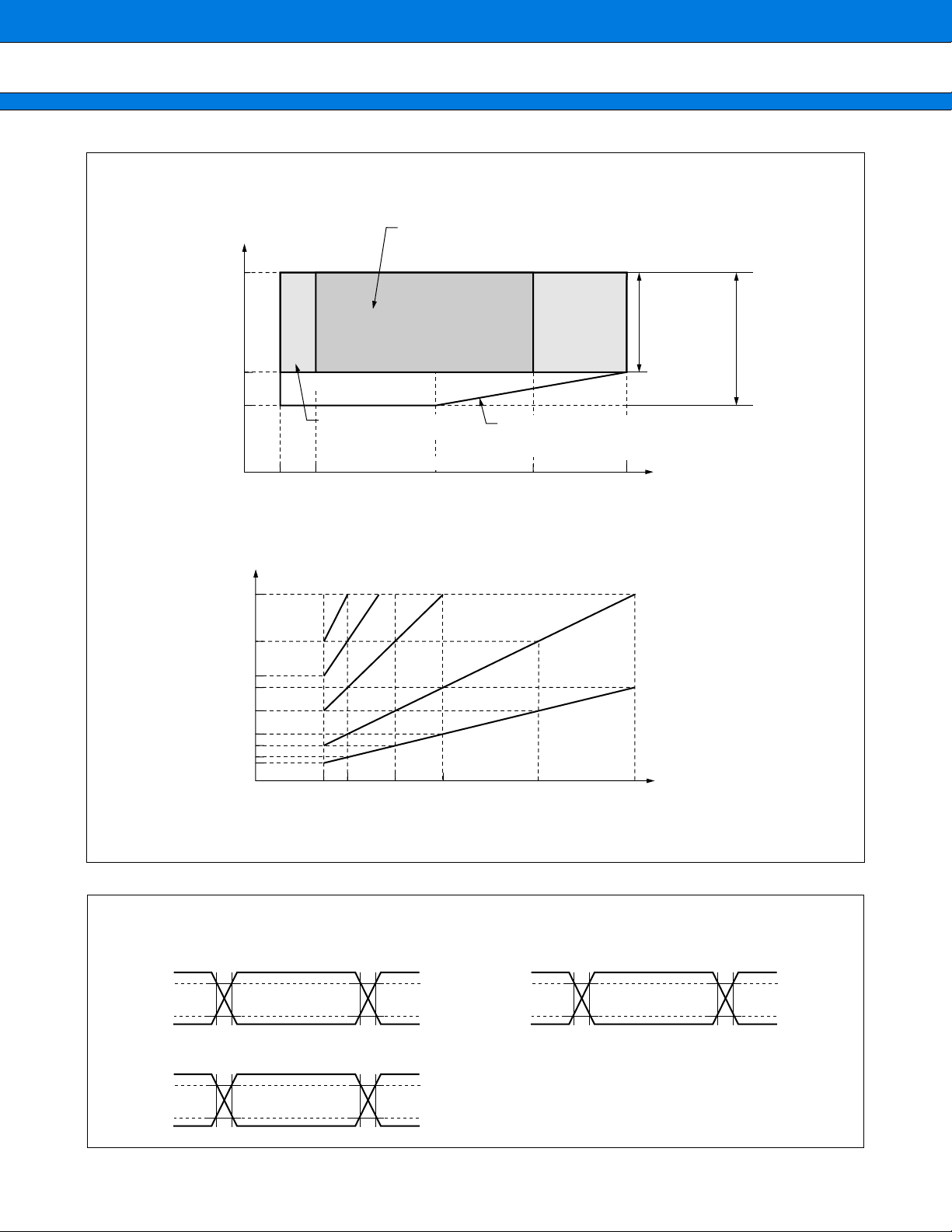
• PLL guaranteed operation range
e
Relationship between internal operating clock frequency and power supply voltage
3.6
MB90560/565 Series
PLL guaranteed operation range
(MB90567/568/F568 : 3.0 V to 3.6 V, fCP = 3 MHz to 16 MHz)
(MB90V560 : 3.0 V to 3.6 V, fCP = 3 MHz to 12 MHz)
Supply Voltage VCC (V)
3.0
2.7
Guaranteed operation range
for MB90V560
(3.0 V to 3.6 V,
CP = 1.5 MHz to 12 MHz)
f
1.5 3 8 12 16
Internal Clock fCP (MHz)
Guaranteed operation range for MB90567/568/F568
(3.0 V to 3.6 V, f
(2.7 V to 3.6 V, fCP = 1.5 MHz to 8 MHz)
CP = 1.5 MHz to 16 MHz)
PLL guaranteed
operation range
A/D converter
guaranteed
operation rang
Relationship between oscillation frequency and internal operating clock frequency
16
12
9
8
6
4
3
Internal Clock fCP (MHz)
2
1.5
×4 ×3 ×2 ×1
No multiplier
34 6 8
Source Oscillation Clock fC (MHz)
12 16
The AC ratings are specified for the following measurement reference voltages.
•
Input signal waveform
Hysteresis input pin
0.8 VCC
0.2 VCC
•
Output signal waveform
Output pin
2.4 V
0.8 V
Pins other than hysteresis input or MD input pins
0.7 V
CC
0.3 VCC
75
Page 76

MB90560/565 Series
(2) Reset
Parameter Symbol Pin Name Condition
(T
A = −40 °C to +85 °C, VCC = 2.7 V to 3.6 V, VSS = AVSS = 0.0 V)
Value
Unit Remarks
Min. Max.
In normal
operation
In stop
mode
Reset input time t
RSTL RST
16 t
CP ns
Oscillator oscillation
time* + 16 t
CP
ms
*: Oscillator oscillation time is the time to reach 90% amplitude. For a crystal oscillator, this is a few to several
dozen ms; for a F AR/ceramic oscillator, this is se veral hundred µs to a f ew ms, and for an external clock this is 0 ms .
• In normal operation
tRSTL
RST
0.2 VCC
0.2 VCC
• In stop mode
tRSTL
RST
0.2Vcc
0.2Vcc
76
X0
Internal
operation
clock
Internal
reset
90 % of
amplitude
Oscillator
oscillation time
16 tcp
Oscillator stabilization wait time
Execution of the instruction
Page 77
(3) Power-On Reset
(T
A = −40 °C to +85 °C, VCC = 2.7 V to 3.6 V, VSS = AVSS = 0.0 V)
Parameter Symbol Pin Name
Power supply rise time t
R VCC
Condi-
tion
*
Value
Min. Max.
0.05 30 ms
Power supply cutoff time t
* : V
CC must be less than 0.2 V before power-on.
OFF VCC 4 ms For repeated operation
Notes : • The above rating values are for generating a power-on reset.
• Some internal registers are only initialized by a power-on reset. Always apply the power supply in
accordance with the above ratings if you wish to initialize these registers.
tR
MB90560/565 Series
Unit Remarks
VCC
2.7 V
0.2 V0.2 V
t
OFF
0.2 V
Sudden changes in the power supply voltage may cause a power-on reset.
The recommended practice if you wish to change the power supply voltage while the device is
operating is to raise the voltage smoothly as shown below. Also, changes to the supply voltage
should be performed when the PLL clock is not in use. The PLL clock may be used, however, if
the rate of voltage change is 1 V/s or less.
VCC
Recommended rate of voltage
rise is 50 mV/ms or less.
2.5 V
V
SS
Maintain RAM data
77
Page 78
MB90560/565 Series
(4) UART0 and UART1
Parameter Symbol Pin Name Condition
(T
A = −40 °C to +85 °C, VCC = 2.7 V to 3.6 V, VSS = AVSS = 0.0 V)
Value
Unit Remarks
Min. Max.
Serial clock cycle time t
SCK ↓ → SOT delay time t
SCYC SCK0, SCK1
SLOV
SCK0, SCK1
SOT0, SOT1
Internal shift clock
8 t
CP ns
−80 80 ns
mode, output pin
Valid SIN → SCK ↑ t
SCK ↑ → valid SIN hold time t
Serial clock “H” pulse width t
SCK0, SCK1
IVSH
SHIX
SHSL SCK0, SCK1
SIN0, SIN1
SCK0, SCK1
SIN0, SIN1
load is
L = 80 pF + 1 TTL
C
100 ns
60 ns
CP ns
4 t
Serial clock “L” pulse width tSLSH SCK0, SCK1 4 tCP ns
SCK ↓ → SOT delay time t
Valid SIN → SCK ↑ t
SCK ↑ → valid SIN hold time t
SLOV
IVSH
SHIX
SCK0, SCK1
SOT0, SOT1
SCK0, SCK1
SIN0, SIN1
SCK0, SCK1
SIN0, SIN1
External shift clock
mode, output pin
load is
C
L = 80 pF + 1 TTL
150 ns
60 ns
60 ns
Notes : • These are the AC ratings for CLK synchronous mode.
• CV is the load capacitor connected to the pin for testing.
• t
CP is the machine cycle period (unit = ns)
78
Page 79

•
Internal shift clock mode
SCK
SOT
SIN
•
External shift clock mode
SCK
MB90560/565 Series
tSCYC
2.4 V
0.8 V 0.8 V
tSLOV
2.4 V
0.8 V
tIVSH tSHIX
0.8 V
CC
0.2 VCC
tSLSH tSHSL
0.8 VCC 0.8 VCC
0.2 VCC 0.2 VCC
0.8 VCC
0.2 VCC
SOT
SIN
tSLOV
2.4 V
0.8 V
tIVSH tSHIX
0.8 V
CC
0.2 VCC
0.8 VCC
0.2 VCC
79
Page 80

MB90560/565 Series
(5) Timer Input Timings
Parameter Symbol Pin Name
(T
A = −40 °C to +85 °C, VCC = 2.7 V to 3.6 V, VSS = AVSS = 0.0 V)
Condi-
tion
Value
Unit Remarks
Min. Max.
Input pulse width t
FRCK
TIN0 to 1
TIWH, tTIWL FRCK, TIN0, TIN1 4 tCP ns
0.8 VCC
tTIWH tTIWL
0.8 VCC
0.2 VCC 0.2 VCC
(6) Timer Output Timings
(T
A = −40 °C to +85 °C, VCC = 2.7 V to 3.6 V, VSS = AVSS = 0.0 V)
Parameter Symbol Pin Name Condition
CLK ↑ → T
time
OUT change
CLK
tTO
RTO0 to RTO5, PPG0 to PPG5
TO0, TO1
2.4 V
t
TO
Value
Unit Remarks
Min. Max.
30 ns
T
OUT
(7) Trigger Input Timings
Parameter Symbol Pin Name Condition
Input pulse width t
INT0 to INT7
IN0 to IN3
80
2.4 V
0.8 V
A = −40 °C to +85 °C, VCC = 2.7 V to 3.6 V, VSS = AVSS = 0.0 V)
(T
TRGL INT0 to INT7, IN0 to IN3
0.8 VCC
tTRGH tTRGL
0.8 VCC
0.2 VCC 0.2 VCC
Value
Unit Remarks
Min. Max.
5 t
CP ns
In normal
operation
1 µs In stop mode
Page 81

MB90560/565 Series
5. Electrical Characteristics for the A/D Converter
(MB90567/568/F568 : TA = −40 °C to +85 °C, 2.7 V ≤ AVR, VCC = AVCC = 2.7 V to 3.6 V, VSS = AVSS = 0.0 V)
(MB90V560 : TA = +25 °C, 3.0 V ≤ AVR, VCC = AVCC = 3.0 V to 3.6 V, VSS = AVSS = 0.0 V)
Parameter Symbol Pin Name
Min. Typ. Max.
Resolution 10 bit
Total error ±3.0 LSB
Non-linearity error ±2.5 LSB
Value
Unit Remarks
Differential linearity
error
Zero transition
voltage
Full-scale transition
voltage
Conversion time 66 t
Sampling time 32 t
Analog port input
current
Analog input voltage V
±1.9 LSB
V
OT AN0 to AN7
V
FST AN0 to AN7
AVSS
−1.5 LSB
AVR
−3.5 LSB
SS
AV
+0.5
+2.5 LSB
AVR
−1.5 LSB
+0.5 LSB
CP ns
CP ns
IAIN AN0 to AN7 10 µA
AIN AN0 to AN7 0 AVR V
Reference voltage AVR 2.7 AV
A AVCC 15mA
I
Power supply current
IAH AVCC 5 µA*
R AVR 100 200 µA
Reference voltage
supply current
Variation between
channels
* : Current when A/D converter is not used and CPU is in stop mode (V
I
I
RH AVR 5 µA*
AN0 to AN7 4LSB
CC = AVCC = AVR = 3.3 V)
SS
AV
AVR
CC V
mV
1 LSB = AVRH/1024
mV
Notes : • The L reference voltage is fixed to AV
• Ensure that the output impedance of the e xternal circuit connected to the analog input meets the following
condition :
Output impedance of MB90F568 external circuit ≤ 14 kΩ (Sampling Time = 4 µs)
Output impedance of MB90567/568 external circuit ≤ 7 kΩ (Sampling Time = 4 µs)
• If the output impedance of the external circuit is too high, the analog voltage sampling time may be too short.
SS. The relative error increases as AVR becomes smaller.
81
Page 82

MB90560/565 Series
•
Equivalent circuit of analog input circuit
CRON
Comparator
Analog input
MB90567/568/F568
R
ON = 7.1 kΩ approx.
C = 48.3 pF approx.
Note : The values listed are an indication only.
82
Page 83

6. Flash Memory Erase and Programming Performance
MB90560/565 Series
Parameter Condition
Sector erase time
T
Chip erase time 5 s
Word (16 bit width)
programming time
Erase/Program cycle 10,000 cycle
Data holding time 100,000 h
• Points to note regarding the MB90F568, 567, and 568 specifications
This section describes the specification differences between the MB90F568/567/568 and the MB90F562/F562B/
562/562A/561/561A.
(1) Functional differences
1) The 5 V to 3 V regulator has been removed in the MB96565 series.
The C pin has been changed to an N.C. pin.
2) The A/D converter unit in the MB96565 series has changed from a 5 V version to a 3 V version.
However, the conversion time and sampling time remain the same.
A = + 25 °C
Vcc = 3.3 V
Min Typ Max
115s
16 3,600 µs Excludes system-level overhead
Value
Units Remarks
Excludes 00H programming prior
erasure
Excludes 00H programming prior
erasure
3) The maximum voltage that can be applied to I/O pins has changed from 5 V to 3 V in the MB96565 series.
4) Added transfer counter clear function to UART in the MB96565 series.
This function restores the UART to its initial state when “0” is written to the UART reset bit.
(2) Points to note when using the devices
The MB90F562, F562B, and F568 use P60 (14) as SIN1, P61 (15) as SOT1, and P40 (60) as SCK0 when
performing on-board programming.
Use the following pin settings when performing on-board programming.
Pin Name Pin I/O Level* Remarks
MD2 “H” level
Serial write mode settingsMD1 “H” level
MD0 “L” level
SIN1 Serial data input Normally shared with P60
SOT1 Serial data output Normally shared with P61
SCK0 Serial clock Normally shared with P40
P00 “L” level
P01 “H” level Input “L” level for PC writing
* : These settings are for using a Yokogawa Digital Computer Corporation writer f or on-board prog r amming. Alter-
natively, writing can be performed from a PC, but a special write program is required.
83
Page 84

MB90560/565 Series
EXAMPLE CHARACTERISTICS
■
60
TA = +25 °C
50
40
30
ICC (mA)
20
10
0
2 2.5 3 3.5
40
TA = +25 °C
35
30
25
(mA)
20
15
ICC3
10
5
0
2 2.5 3 3.5
MB90F568 ICC − VCC
16 MHz
12 MHz
8 MHz
4 MHz
2 MHz
4 4.5
VCC (V)
MB90568 ICC − VCC
16 MHz
12 MHz
8 MHz
4 MHz
2 MHz
4 4.5
VCC (V)
84
MB90F568 ICCS − VCC
20
TA = +25 °C
18
16
14
12
(mA)
10
8
ICCS
6
4
2
0
2 2.5 3 3.5
VCC (V)
16 MHz
12 MHz
8 MHz
4 MHz
2 MHz
4 4.5
(Continued)
Page 85

(mA)
CCS
I
40
TA = +25 °C
35
MB90568 ICCS − VCC
18
TA = +25 °C
16
14
12
10
8
6
4
2
0
2 2.5 3 3.5
VCC (V)
MB90F562 ICC − VCC
MB90560/565 Series
16 MHz
12 MHz
8 MHz
4 MHz
2 MHz
4 4.5
f = 16 MHz
30
25
20
(mA)
ICC
15
10
5
0
2.5 3 3.5 4 4.5
MB90562 ICC − VCC
70
TA = +25 °C
60
50
40
30
ICC (mA)
20
10
0
2.5 3 3.5 4 4.5
f = 12 MHz
f = 10 MHz
f = 8 MHz
f = 4 MHz
f = 2 MHz
5 5.5 6 6.5
VCC (V)
f = 16 MHz
f = 12 MHz
f = 10 MHz
f = 8 MHz
f = 4 MHz
f = 2 MHz
5 5.5 6 6.5
VCC (V)
(Continued)
85
Page 86

MB90560/565 Series
(Continued)
16
TA = +25 °C
14
12
10
8
ICCS (mA)
6
MB90F562 ICCS − VCC
f = 16 MHz
f = 12 MHz
f = 10 MHz
f = 8 MHz
4
2
0
2.5 3 3.5 4 4.5
MB90562 ICCS − VCC
30
TA = +25 °C
25
20
15
ICCS (mA)
10
5
0
2.5 3 3.5 4 4.5
f = 4 MHz
f = 2 MHz
5 5.5 6 6.5
VCC (V)
f = 16 MHz
f = 12 MHz
f = 10 MHz
f = 8 MHz
f = 4 MHz
f = 2 MHz
5 5.5 6 6.5
VCC (V)
86
Page 87

ORDERING INFORMATION
■
•
MB90560 series
Part No. Package Remarks
MB90561P
MB90562P
MB90561AP
MB90562AP
MB90F562P
MB90F562BP
MB90561PF
MB90562PF
MB90561APF
MB90562APF
MB90F562PF
MB90F562BPF
MB90561PFM
MB90562PFM
MB90561APFM
MB90562APFM
MB90F562PFM
MB90F562BPFM
MB90560/565 Series
64-pin plastic SH-DIP
(DIP-64P-M01)
64-pin plastic QFP
(FPT-64P-M06)
64-pin plastic LQFP
(FPT-64P-M09)
•
MB90565 series
Part No. Package Remarks
MB90567PF
MB90568PF
MB90F568PF
MB90567PFM
MB90568PFM
MB90F568PFM
64-pin plastic QFP
(FPT-64P-M06)
64-pin plastic LQFP
(FPT-64P-M09)
87
Page 88
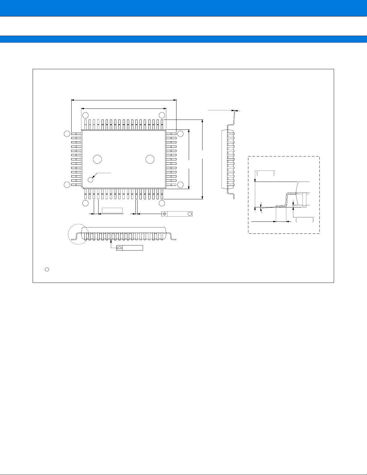
MB90560/565 Series
PACKAGE DIMENSIONS
■
64-pin plastic QFP
(FPT-64P-M06)
52
64
119
"A"
24.70±0.40(.972±.016)
20.00±0.20(.787±.008)
INDEX
1.00(.039)
0.10(.004)
0.10(.004)
Note : Pins width and pins thickness include plating thickness.
0.17±0.06
18.70±0.40
(.736±.016)
(.007±.002)
Details of "A" part
+0.35
–0.20
3.00
(Mounting height)
+.014
–.008
.118
0~8°
1.20±0.20
(.047±.008)
0.42±0.08
(.017±.003)
3351
32
14.00±0.20
(.551±.008)
20
0.20(.008)
M
+0.15
–0.20
0.25
+.006
–.008
.010
(Stand off)
C
2001 FUJITSU LIMITED F64013S-c-4-4
Dimensions in mm (inches).
Note: The values in parentheses are reference values.
(Continued)
88
Page 89

MB90560/565 Series
64-pin plastic LQFP
(FPT-64P-M09)
14.00±0.20(.551±.008)SQ
12.00±0.10(.472±.004)SQ
49
INDEX
64
116
0.65(.026)
Note : Pins width and pins thickness include plating thickness.
0.145±0.055
3348
0.32±0.05
(.013±.002)
32
17
0.13(.005)
M
(.0057±.0022)
0.10(.004)
0.10(.004)
"A"
Details of "A" part
+0.20
–0.10
1.50
+.008
–.004
.059
0.25(.010)
0~8°
0.50±0.20
(.020±.008)
0.60±0.15
(.024±.006)
(Mounting height)
0.10±0.10
(.004±.004)
(Stand off)
C
2001 FUJITSU LIMITED F64018S-c-2-4
Dimensions in mm (inches).
Note: The values in parentheses are reference values.
(Continued)
89
Page 90
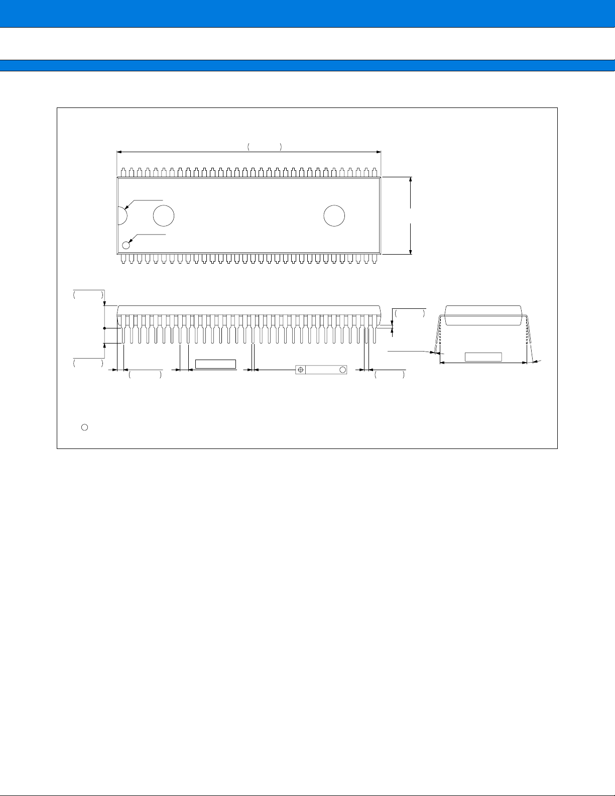
MB90560/565 Series
(Continued)
64-pin plastic SH-DIP
(DIP-64P-M01)
Note : Pins width and pins thickness include plating thickness.
+0.22
–0.55
58.00
INDEX-1
INDEX-2
+0.70
–0.20
4.95
+.028
–.008
.195
+0.20
–0.30
3.30
+.008
.130 –.012
C
2001 FUJITSU LIMITED D64001S-c-4-5
1.378
.0543
+0.40
–0.20
+.016
–.008
1.778(.0700)
2.283
0.47±0.10
(.019±.004)
+.009
–.022
0.25(.010)
17.00±0.25
(.669±.010)
+0.50
–0.19
0.70
+.020
–.007
.028
0.27±0.10
(.011±.004)
+0.50
–0
M
1.00
.039 –.0
+.020
19.05(.750)
0~15°
Dimensions in mm (inches).
Note: The values in parentheses are reference values.
90
Page 91

MB90560/565 Series
FUJITSU LIMITED
All Rights Reserved.
The contents of this document are subject to change without notice.
Customers are advised to consult with FUJITSU sales
representatives before ordering.
The information and circuit diagrams in this document are
presented as examples of semiconductor device applications, and
are not intended to be incorporated in devices for actual use. Also,
FUJITSU is unable to assume responsibility for infringement of
any patent rights or other rights of third parties arising from the use
of this information or circuit diagrams.
The products described in this document are designed, developed
and manufactured as contemplated for general use, including
without limitation, ordinary industrial use, general office use,
personal use, and household use, but are not designed, developed
and manufactured as contemplated (1) for use accompanying fatal
risks or dangers that, unless extremely high safety is secured, could
have a serious effect to the public, and could lead directly to death,
personal injury, severe physical damage or other loss (i.e., nuclear
reaction control in nuclear facility, aircraft flight control, air traffic
control, mass transport control, medical life support system, missile
launch control in weapon system), or (2) for use requiring
extremely high reliability (i.e., submersible repeater and artificial
satellite).
Please note that Fujitsu will not be liable against you and/or any
third party for any claims or damages arising in connection with
above-mentioned uses of the products.
Any semiconductor devices have an inherent chance of failure. You
must protect against injury, damage or loss from such failures by
incorporating safety design measures into your facility and
equipment such as redundancy, fire protection, and prevention of
over-current levels and other abnormal operating conditions.
If any products described in this document represent goods or
technologies subject to certain restrictions on export under the
Foreign Exchange and Foreign Trade Law of Japan, the prior
authorization by Japanese government will be required for export
of those products from Japan.
F0204
FUJITSU LIMITED Printed in Japan
 Loading...