


查询MB90550A供应商
FUJITSU SEMICONDUCTOR
DATA SHEET
DS07-13706-2E
16-bit Proprietary Microcontroller
CMOS
F2MC-16LX MB90550A/550B Series
MB90552A/552B/553A/553B/T552A/T553A
MB90F553A/P553A
DESCRIPTION
■■■■
The MB90550A/550B series is a line of general-purpose, high-performance, 16-bit microcontrollers designed for
applications which require high-speed real-time processing, such as industrial machines, OA equipment, and
process control systems.
While inheriting the AT architecture of the F
incorporates additional instructions for high-level languages , supports extended addressing modes, and contains
enhanced multiplication and division instructions as well as a substantial collection of improved bit manipulation
instructions. In addition, the MB90550A/550B has an on-chip 32-bit accumulator which enables processing of
long-word data.
MB90552B and MB90553B are radiation noise decreased type. There are no change in the functional specification.
2
*: F
MC stands for FUJITSU Flexible Microcontroller, a registered trademark of FUJITSU LIMITED.
2
MC*-8 family, the instruction set for the MB90550A/550B series
FEATURES
■■■■
• Minimum instruction execution time: 62.5 ns (at oscillation of 4 MHz, × four times the PLL clock)
• Maximum memory space: 16 Mbytes
• Instruction set optimized for controller applications
Supported data types: Bit, byte, word and long word
Typical addressing mode: 23 types
Enhanced precision calculation realized by 32-bit accumulator
Enhanced signed multiplication/division instruction and RETI instruction functions
PACKAGES
■■■■
100-pin plastic QFP 100-pin plastic LQFP
(FPT-100P-M06) (FPT-100P-M05)
(Continued)

MB90550A/550B Series
(Continued)
• Instruction set designed for high level language (C) and multi-task operations
Adoption of system stack pointer
Symmetrical instruction set and barrel shift instructions
• Integrated address match detection function (for two address pointers)
• Faster execution speed: 4-byte queue
• Powerful interrupt functions (Eight priority levels programmable)
External interrupt inputs: 8 channels
• Data transfer functions (Intelligent I/O service): Up to 16 channels
DTP request inputs: 8 channels
• Embedded ROM size (EPROM, Flash: 128 Kbytes)
Mask ROM: 64 Kbytes/128 Kbytes
• Embedded RAM size (EPROM, Flash: 4 Kbytes)
Mask ROM: 2 Kbytes/4 Kbytes
• General-purpose por ts: Up to 83 channels
(Input pull-up resistor settable for: 16 channels; Open drain settable for: 8 channels; I/O open drains: 6 channels)
• A/D converter (RC successive approximation type): 8 channels
(Resolution: 8 or 10 bits selectable; Conversion time of 26.3 µs minimum)
• UART: 1 channel
• Extended I/O serial interface: 2 channels
2
•I
C interface: 2 channels
(Two channels, including one s witchable between terminal input and output)
• 16-bit reload timer: 2 channels
• 8/16-bit PPG timer: 3 channels
(8 bits × 2 channels; 16 bits x 1 channel: Mode switching function provided)
• 16-bit I/O timer
(Input capture × 4 channels, output compare × 4 channels, free run timer ×1 channel)
• Clock monitor function integrated (Delivering the oscillation clock divided by 21 to 28)
• Timebase timer/watchdog timer: 18 bits
• Low power consumption modes (sleep, stop, hardware standby, and CPU intermittent operation modes)
• Package: QFP-100, LQFP-100
•CMOS technology
2
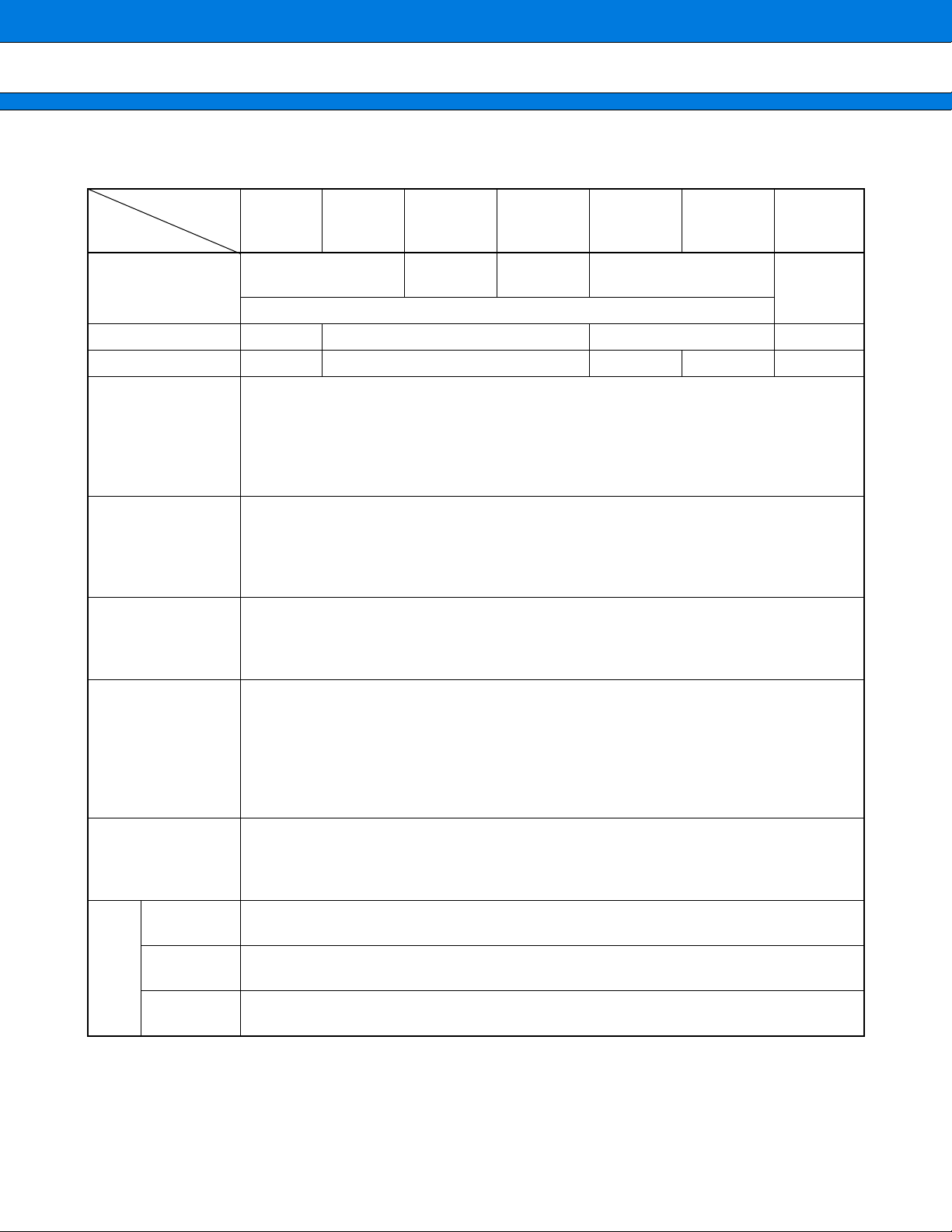
PRODUCT LINEUP
■■■■
MB90550A/550B Series
Part number
Item
Classification
ROM size 64 Kbytes 128 Kbytes None None
RAM size 2 Kbytes 4 Kbytes 2 Kbytes 4 Kbytes 6 Kbytes
CPU functions
Ports
UART (SCI)
MB90552A
MB90552B
Mask ROM products
Interrupt processing time: 1.5 ms (at machine clock of 16 MHz, minimum value)
MB90553A
MB90553B
Minimum execution time: 62.5 ns (at machine clock of 16 MHz)
General-purpose I/O ports (N-channel open-drain output): 6
General-purpose I/O ports (N-channel open-drain function selectable): 8
Clock synchronized transmission (62.5 Kbps to 2 Mbps)
Clock asynchronized transmission (62500 bps to 9615 bps)
Transmission can be performed by bi-directional serial transmission or by
MB90F553A MB90P553A MB90T552A MB90T553A MB90V550A
Flash ROM
products
Mass Product
The number of instructions: 340
Instruction bit length: 8 bits, 16 bits
Instruction length: 1 byte to 7 bytes
Data bit length: 1 bit, 8 bits, 16 bits
General-purpose I/O ports (CMOS output): 53
General-purpose I/O ports (with pull-up resistor): 16
master/slave connection.
OTP External ROM products
Total: 83
Evaluation
product
8/10-bit A/D
converter
8/16-bit PPG timer
16-bit
free run timer
16-bit
I/O
timer
Output compare (OCU)
Input capture
(ICU)
Conversion precision: 8/10-bit can be selectively used.
Number of inputs: 8
One-shot conversion mode (converts selected channel only once)
Scan conversion mode (converts two or more successive channels and can program up to
8 channels.)
Continuous conversion mode (converts selected channel continuously)
Stop conversion mode (converts selected channel and stop operation repeatedly)
Number of channels: 1 (8-bit × 2 channels)
PPG operation of 8-bit or 16-bit
A pulse wave of given intervals and given duty ratios can be output.
Pulse interval: 62.5 ns to 1 ms (at oscillation of 4 MHz, machine clock of 16 MHz)
Number of channels: 1
Overflow interrupts
Number of channels: 4
Pin input factor: A match signal of compare register
Number of channels: 4
Rewriting a register value upon a pin input (rising, falling or both edges)
(Continued)
3

MB90550A/550B Series
(Continued)
Part number
Item
MB90552A
MB90552B
MB90553A
MB90553B
MB90F553A MB90P553A MB90T552A MB90T553A MB90V550A
DTP/external
interrupt circuit
Extended I/O serial
Started by a rising edge, a falling edge, an “H” level input, or an “L” level input.
External interrupt circuit or extended intelligent I/O service (EI
Clock synchronized transmission (3125 bps to 1 Mbps)
interface
2
I
C interface Serial I/O port for supporting Inter IC BUS
Number of inputs: 8
LSB first/MSB first
2
OS) can be used.
18-bit counter
Timebase timer
Interrupt interval: 1.024 ms, 4.096 ms, 16.384 ms, 131.072 ms
(at oscillation of 4 MHz)
Watchdog timer
Reset generation interval: 3.58 ms, 14.33 ms, 57.23 ms, 458.75 ms
(at oscillation of 4 MHz, minimum value)
Process CMOS
Power supply volt-
age for operation*
4.5 V to 5.5 V
*:Varies with conditions such as the operating frequency. (See section “■ ELECTRICAL CHARA CTERISTICS”)
Assurance for the MB90V550A is given only for operation with a tool at a power voltage of 4.5 V to 5.5 V, an
operating temperature of 0°C to +25°C, and an operating frequency of 1 MHz to 16 MHz.
PACKAGE AND CORRESPONDING PRODUCTS
■■■■
Package
MB90552A
MB90552B
MB90553A
MB90553B
MB90F553A MB90P553A
FPT-100P-M05 ×
FPT-100P-M06
: Available ×: Not available
Note:For more info rmation about each package, see section “■ PACKAGE DIMENSIONS”
DIFFERENCES AMONG PRODUCTS
■■■■
Memory Size
In evaluation with an evaluation product, note the difference between the evaluation product and the product
actually used. The following items must be taken into consideration.
• The MB90V550A does not have an internal ROM. However, operations equivalent to those performed by a
chip with an internal ROM can be evaluated b y using a dedicated dev elopment tool, enabling selection of ROM
size by setting the development tool.
• In the MB90V550A, images from FF4000
H to FFFFFFH are mapped to bank 00, and FE0000H to FF3FFFH
are mapped to bank FE and FF only. (This setting can be changed by configuring the development tool.)
• In the MB90F553A/553A/553B/552A/552B, images from FF4000
H to FFFFFFH are mapped to bank 00, and
FF0000H to FF3FFFH to bank FF only.
4

PIN ASSIGNMENTS
■■■■
• FPT-100P-M06
MB90550A/550B Series
(Top View)
P20/A16
P21/A17
P22/A18
P23/A19
P24/A20
P25/A21
P26/A22
P27/A23
P30/ALE
P31/RD
V
P32/WRL
P33/WRH
P34/HRQ
P35/HAK
P36/RDY
P37/CLK
P40/SCK
P41/SOT
P42/SIN
P43/SCK1
P44/SOT1
V
P45/SIN1
P46/ADTG
P47/SCK0
P50/SDA0/SOT0
P51/SCL0/SIN0
P52/SDA1
P17/AD15
P16/AD14
P15/AD13
P14/AD12
P13/AD11
P12/AD10
P11/AD09
P10/AD08
P07/AD07
P06/AD06
P05/AD05
P04/AD04
P03/AD03
P02/AD02
P01/AD01
P00/AD00
VCCX1X0V
99989796959493929190898887868584838281
100
1
2
3
4
5
6
7
8
9
10
11
SS
12
13
14
15
16
17
18
19
20
21
22
CC
23
24
25
26
C
27
28
29
30
SS
80
PA4/CKOT
79
PA3
78
PA2
77
RST
76
PA1/OUT3
75
PA0/OUT2
74
P97/PPG5
73
P96/PPG4
72
P95/PPG3
71
P94/PPG2
70
P93/PPG1
69
P92/PPG0
68
P91/OUT1
67
P92/OUT0
66
P87/IN3
65
P86/IN2
64
P85/IN1
63
P84/IN0
62
P83/TOT1
61
P82/TOT0
60
P81/TIN1
59
P80/TIN0
58
P77/IRQ7
57
P76/IRQ6
56
P75/IRQ5
55
P74/IRQ4
54
P73/IRQ3
53
P72/IRQ2
52
HST
MD2
51
31323334353637383940414243444546474849
P53/SCL1
CC
AV
P55/SCL2
P54/SDA2
AVRL
AVRH
SS
AV
P60/AN0
P61/AN1
SS
V
P62/AN2
P63/AN3
P64/AN4
P65/AN5
P66/AN6
P67/AN7
P70/IRQ0
P71/IRQ1
MD0
(FPT-100P-M06)
50
MD1
5

MB90550A/550B Series
• FPT-100P-M05
P21/A17
P20/A16
P17/AD15
P16/AD14
P15/AD13
P14/AD12
P13/AD11
P12/AD10
P11/AD09
P10/AD08
100999897969594939291908988878685848382818079787776
(Top view)
P07/AD07
P06/AD06
P05/AD05
P04/AD04
P03/AD03
P02/AD02
P01/AD01
CC
X1X0VSSPA4/CKOT
P00/AD00
V
PA3
PA2
P22/A18
P23/A19
P24/A20
P25/A21
P26/A22
P27/A23
P30/ALE
P31/RD
V
P32/WRL
P33/WRH
P34/HRQ
P35/HAK
P36/RDY
P37/CLK
P40/SCK
P41/SOT
P42/SIN
P43/SCK1
P44/SOT1
V
P45/SIN1
P46/ADTG
P47/SCK0
1
2
3
4
5
6
7
8
9
SS
10
11
12
13
14
15
16
17
18
19
20
CC
21
22
23
24
25
C
26272829303132333435363738394041424344454647484950
CC
AV
P53/SCL1
P52/SDA1
P55/SCL2
P54/SDA2
AVRL
AVRH
SS
AV
P60/AN0
P61/AN1
P62/AN2
P63/AN3
SS
V
P64/AN4
P65/AN5
P66/AN6
P67/AN7
MD0
P70/IRQ0
P71/IRQ1
MD1
MD2
HST
75
RST
74
PA1/OUT3
73
PA0/OUT2
72
P97/PPG5
71
P96/PPG4
70
P95/PPG3
69
P94/PPG2
68
P93/PPG1
67
P92/PPG0
66
P91/OUT1
65
P90/OUT0
64
P87/IN3
63
P86/IN2
P85/IN1
62
61
P84/IN0
60
P83/TOT1
59
P82/TOT0
58
P81/TIN1
57
P80/TIN0
56
P77/IRQ7
55
P76/IRQ6
P75/IRQ5
54
53
P74/IRQ4
P73/IRQ3
52
51
P72/IRQ2
P51/SCL0/SIN0
P50/SDA0/SOT0
(FPT-100P-M05)
6

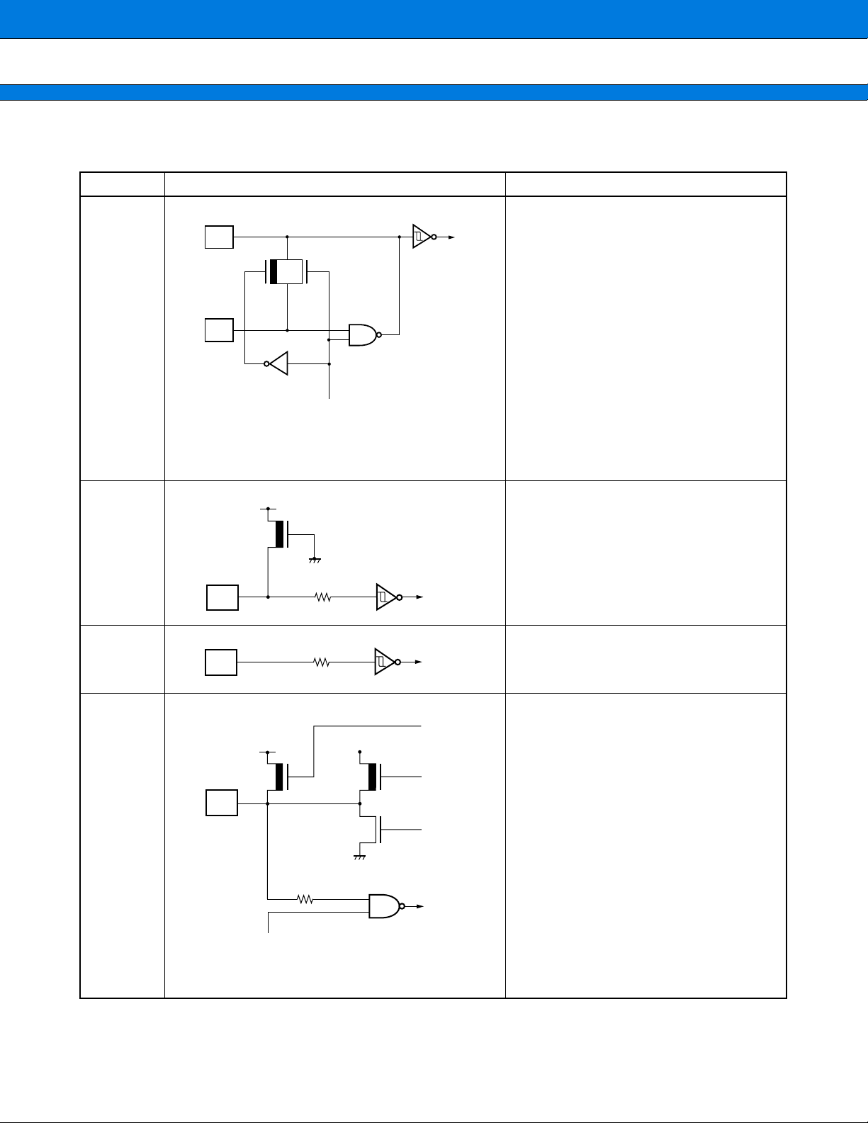
PIN DESCRIPTION
■■■■
MB90550A/550B Series
Pin no.
QFP LQFP
82 80 X0 A Oscillation pin
83 81 X1 A Oscillation pin
77 75 RST
52 50 HST C Hardware standby input pin
85 to 92 83 to 90
93 to
100
1 to 8
91 to 98
99,100,
1 to 6
97
Pin name Circuit type Function
B Reset input pin
General-purpose I/O ports.
P00 to P07
D
(CMOS)
AD00 to
AD07
P10 to P17
D
(CMOS)
AD08 to
AD15
P20 to P27
E
(CMOS)
A16 to A23
P30
E
(CMOS)
ALE
A pull-up resistor can be added (RD07 to RD00 = 1) by using
the pull-up resistor setting register (RDR0).
D07 to D00 = 1: Disabled when the port is set for output.
Serve as lower data I/O/lower address output (AD00 to AD07)
pins in the external bus mode.
General-purpose I/O ports.
A pull-up resistor can be added (RD17 to RD10 = 1) by using the
pull-up resistor setting register (RDR1).
D17 to D10 = 1: Disabled when the port is set for output.
Serve as upper data I/O/middle address output (AD08 to AD15)
pins in the 16-bit bus-width, external bus mode.
General-purpose I/O ports.
This function is enabled either in single-chip mode or with the
external address output control register set to “Port”.
External address bus A16 to A23 output pins.
This function is enabled in an external-bus enabled mode with
the external address output register set to “Address”.
General-purpose I/O port.
This function is enabled in single-chip mode.
Address latch enable output pin.
This function is enabled in an external-bus enabled mode.
10 8
12 10
13 11
P31
RD
P32
WRL
P33
WRH
E
(CMOS)
E
(CMOS)
E
(CMOS)
General-purpose I/O port.
This function is enabled in single-chip mode.
Read strobe output pin for the data bus.
This function is enabled in an external-bus enabled mode.
General-purpose I/O port.
This function is enabled in single-chip mode.
Write strobe output pin for the lower eight bits of the data bus.
This function is enabled in an external-bus enabled mode.
General-purpose I/O port.
This function is enabled in single-chip mode.
Write strobe output pin for the upper eight bits of the data bus.
This function is enabled in an external-bus enabled mode.
(Continued)
7

MB90550A/550B Series
Pin no.
QFP LQFP
14 12
15 13
16 14
17 15
18 16
Pin name Circuit type Function
P34
E
(CMOS)
HRQ
P35
E
(CMOS)
HAK
P36
E
(CMOS)
RDY
P37
E
(CMOS)
CLK
P40
F
(CMOS/H)
SCK
General-purpose I/O port.
This function is enabled in single-chip mode
Hold request input pin.
This function is enabled in an external-bus enabled mode.
General-purpose I/O port.
This function is enabled in single-chip mode.
Hold acknowledge output pin.
This function is enabled in an external-bus enabled mode.
General-purpose I/O port.
This function is enabled in single-chip mode.
Ready signal input pin.
This function is enabled in an external-bus enabled mode.
General-purpose I/O port.
This function is enabled in single-chip mode.
CLK output pin.
This function is enabled in an external-bus enabled mode.
General-purpose I/O port.
Serves as an open-drain output port (OD40 = 1) depending on the
setting of the open-drain control setting register (ODR4).
(D40 = 0: Disabled when the port is set for input.)
UART serial clock I/O pin.
This function is enabled with the UART clock output enabled.
19 17
20 18
21 19
P41
SOT
P42
SIN
P43
SCK1
F
(CMOS/H)
F
(CMOS/H)
F
(CMOS/H)
General-purpose I/O port.
Serves as an open-drain output port (OD41 = 1) depending on the
setting of the open-drain control setting register (ODR4).
(D41 = 0: Disabled when the port is set for input.)
UART serial data output pin.
This function is enabled with the UART serial data output enabled.
General-purpose I/O port.
Serves as an open-drain output port (OD42 = 1) depending on the
setting of the open-drain control setting register (ODR4).
(D42 = 0: Disabled when the port is set for input.)
UART serial data input pin. Since this input is used as required while
the UART is operating for input, the output by any other function
must be off unless used intentionally.
General-purpose I/O port.
Serves as an open-drain output port (OD43 = 1) depending on the
setting of the open-drain control setting register (ODR4).
(D43 = 0: Disabled when the port is set for input.)
Extended I/O serial clock I/O pin. This function is enabled with the
extended I/O serial clock output enabled.
(Continued)
8

MB90550A/550B Series
Pin no.
QFP LQFP
22 20
24 22
25 23
Pin name Circuit type Function
General-purpose I/O port.
P44
F
Serves as an open-drain output port (OD44 = 1) depending on
the setting of the open-drain control setting register (ODR4).
(D44 = 0: Disabled when the port is set for input.)
(CMOS/H)
Extended I/O serial data output pin.
SOT1
This function is enabled with the extended I/O serial data output
enabled.
General-purpose I/O port.
P45
F
(CMOS/H)
SIN1
Serves as an open-drain output port (OD45 = 1) depending on
the setting of the open-drain control setting register (ODR4).
(D45 = 0: Disabled when the port is set for input.)
Extended I/O serial data input pin.
Since this input is used as required while the extended I/O serial
interface is operating for input, the output by any other function
must be off unless used intentionally.
General-purpose I/O port.
P46
F
(CMOS/H)
ADTG
Serves as an open-drain output port (OD46 = 1) depending on
the setting of the open-drain control setting register (ODR4).
(D46 = 0: Disabled when the port is set for input.)
A/D converter external trigger input pin.
Since this input is used as required while the A/D converter is operating for input, the output by any other function must be off unless used intentionally.
P47
26 24
F
(CMOS/H)
SCK0
27 25 C —
P50
SDA0
28 26
G
(NchOD/H)
SOT0
General-purpose I/O port.
Serves as an open-drain output port (OD47 = 1) depending on
the setting of the open-drain control setting register (ODR4).
D47 = 0: Disabled when the port is set for input.
Extended I/O serial clock I/O pin. This function is enabled with
the extended I/O serial clock output enabled.
Capacitance pin for regulating the power supply.
Connect an external ceramic capacitor of about 0.1 µF.
N-channel open-drain I/O port.
2
I
C interface data I/O pin.
This function is enabled with the I
2
C interface enabled for
operation.
While the I
2
C interface is operating, place the port output in the
Hi-Z state (PDR = 1).
Extended I/O serial data output pin.
This function is enabled with the extended I/O serial data output
enabled.
(Continued)
9

MB90550A/550B Series
Pin no.
QFP LQFP
29 27
30,32 28,30
31,33 29,31
38 to 41,
43 to 46
36 to 39,
41 to 44
Pin name Circuit type Function
P51
SCL0
G
(NchOD/H)
N-channel open-drain I/O port.
2
I
C interface clock I/O pin. This function is enabled with the
2
I
C interface enabled for operation.
While the I
2
C interface is operating, place the port output in
the Hi-Z state (PDR = 1).
Extended I/O serial data input pin.
SIN0
Since this input is used as required while the extended I/O
serial interface is operating for input, the output by any other
function must be off unless used intentionally.
P52,P54
SDA1,SDA2
G
(NchOD/H)
N-channel open-drain I/O ports.
2
C interface data I/O pins. This function is enabled with the
I
2
I
C interface enabled for operation.
While the I
2
C interface is operating, place the port output in
the Hi-Z state (PDR = 1).
P53,P55
SCL1,SCL2
G
(NchOD/H)
N-channel open-drain I/O ports.
2
C interface clock I/O pins. This function is enabled with the
I
2
I
C interface enabled for operation.
While the I
2
C interface is operating, place the port output in
the Hi-Z state (PDR = 1).
P60 to P67
AN0 to AN7
H
(CMOS/H)
General-purpose I/O ports.
A/D converter analog input pin. This function is enabled with
the analog input enabled.
47,48,
53 to 58
45,46,
51 to 56
59,60 57,58
61,62 59,60
63 to 66 61 to 64
67,68 65,66
P70 to P77
IRQ0 to IRQ7
I
(CMOS/H)
General-purpose I/O ports.
External interrupt request input pins.
Since this input is used as required while external interrupts
remain enabled, the output by any other function must be off
unless used intentionally.
P80,P81
TIN0,TIN1
J
(CMOS/H)
General-purpose I/O ports.
Reload timer event input pins.
Since this input is used as required while the reload timer is
operating for input, the output by any other function must be
off unless used intentionally.
P82,P83
General-purpose I/O ports.
J
TOT0,TOT1
P84 to P87
IN0 to IN3
(CMOS/H)
J
(CMOS/H)
Reload timer output pins.This function is enabled with reroad
timer output enabled.
General-purpose I/O ports.
Input capture trigger input pins.
Since this input is used as required while the input capture
unit is operating for input, the output by any other function
must be off unless used intentionally.
P90,P91
OUT0,OUT1 Output compare event output pins.
J
(CMOS/H)
General-purpose I/O ports.
(Continued)
10

(Continued)
Pin no.
QFP LQFP
MB90550A/550B Series
Pin name Circuit type Function
P92 to P97
69 to 74 67 to 72
PPG0 to
PPG5
PA0,PA1
75,76 73,74
OUT2,OUT3 Output compare event output pins.
78,79 76,77 PA2,PA3
PA4
80 78
CKOT Serves as the CKOT output while the CKOT is operating.
34 32 AV
J
(CMOS/H)
J
(CMOS/H)
J
(CMOS/H)
J
(CMOS/H)
CC A/D converter power-supply pin.
General-purpose I/O ports.
PPG output pins. This function is enabled with the PPG output
enabled.
General-purpose I/O ports.
General-purpose I/O ports.
General-purpose I/O port.
35 33 AVRH A/D converter external reference voltage source pin.
36 34 AVRL A/D converter external reference voltage source pin.
37 35 AV
49,50 47,48 MD0,MD1 C
SS A/D converter power-supply pin.
Operation mode setting input pins.
Connect these pins directly to Vcc or Vss.
Operation mode setting input pin.
K
51 49 MD2
C
Connect this pin directly to Vcc or Vss. (MB90552A/552B/553A/
553B/V550A)
Operation mode setting input pin.
Connect this pin directly to Vcc or Vss. (MB90P553A/F553A)
23,84 21,82 V
11,42,819,40,
79
CC Power (5 V) input pins.
V
SS Power (0 V) input pins.
11
MB90550A/550B Series
I/O CIRCUIT TYPE
■■■■
Type Circuit Remarks
Clock input
X1
• 3 MHz to 32 MHz
• Oscillator recovery resistor approx. 1MΩ
A
X0
HARD,SOFT
STANDBY
CONTROL
• CMOS level hysteresis input
• Pull-up resistor provided
Resistor: About 50 kΩ
B
• CMOS level hysteresis input
C
Pull-up resistor control
• CMOS level output
• CMOS level input
• Standby control provided
Digital output
• Input pull-up resistor control provided
Resistor: About 50 kΩ
12
Digital output
D
Digital input
HARD,SOFT
STANDBY
CONTROL
(Continued)

MB90550A/550B Series
Type Circuit Remarks
• CMOS level output
Digital output
Digital output
E
Digital input
HARD,SOFT
STANDBY
CONTROL
• CMOS level input
• Standby control provided
Open- drain
control
signal
Digital input
• CMOS level output
• CMOS level hysteresis input
• Open-drain control provided
F
Digital input
HARD,SOFT
STANDBY
CONTROL
• N-channel open-drain output
• CMOS level hysteresis input
Digital output
• Standby control provided
Note: Unlike normal CMOS I/O pins, this
pin is not provided with any P-channel
G
Digital input
transistor. Therefore the pin does not allow
a current to flow to the Vcc side even when
applied with a voltage from an external
HARD,SOFT
STANDBY
CONTROL
device with the IC’s power supply left off.
• CMOS level output
Digital output
• CMOS level hysteresis input
• Standby control provided
• Analog input
Digital output
H
HARD,SOFT
STANDBY
CONTROL
A/D
DISABLE
Analog input
Digital input
(Continued)
13

MB90550A/550B Series
(Continued)
Type Circuit Remarks
• CMOS level output
Digital output
Digital output
I
Digital input
HARD
STANDBY
CONTROL
Digital output
• CMOS level hysteresis input
• Standby control provided
• CMOS level output
• CMOS level hysteresis input
• Standby control provided
Digital output
J
Digital input
HARD,SOFT
STANDBY
CONTROL
• CMOS level hysteresis input
• Pull-up resistor provided
Resistor: About 50 kΩ
K
14
MB90550A/550B Series
HANDLING DEVICES
■■■■
1. Preventing Latchup
CMOS ICs may cause latchup in the following situations:
• When a voltage higher than Vcc or lower than Vss is applied to input or output pins.
• When a voltage exceeding the rating is applied between Vcc and Vss.
• When AVcc power is supplied prior to the Vcc voltage.
If latchup occurs, the power supply current increases rapidly, sometimes resulting in thermal breakdown of the
device. Use meticulous care not to let it occur.
For the same reason, also be careful not to let the analog power-supply v oltage e xceed the digital pow er-supply
voltage.
2. Handling unused input pins
Leaving unused input pins open ma y cause a malfunction or latch-up which leads to fatal damage to the de vice .
Therefore they must be pulled up or pulled down through at least 2 kΩ resistance. Also, unused input/output
pins should be left open in output state or handled in the same way as unused input pins.
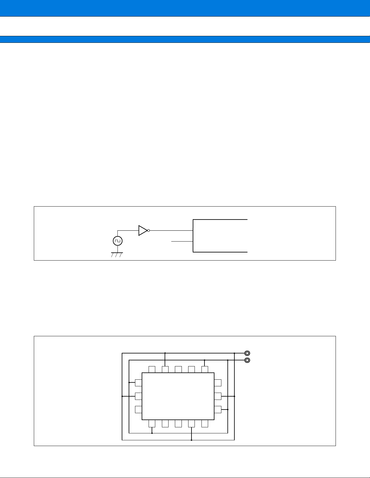
3. Notes on Using External Clock
In using the external clock, drive X0 pin only and leave X1 pin unconnected.
Using external clock
•
MB90550A/550B series
X0
Open
X1
4. Power Supply Pins (VCC/VSS)
In products with multiple VCC or VSS pins, the pins of a same potential are internally connected in the device to
avoid abnormal operations including latch-up. However, the pins should be connected to external power and
ground lines to lower the electro-magnetic emission level and abnormal operation of strobe signals caused by
the rise in the ground level, and to conform to the total current rating.
Make sure to connect V
It is recommended that a bypass capacitor of around 0.1 µF be placed between the V
device.
Using
•
power supply pins
CC and VSS pins via lowest impedance to power lines.
V
CC
V
SS
V
SS
MB90550A/550B
V
V
CC
series
CC
CC and VSS pins near the
V
CC
V
SS
V
SS
V
V
SS
CC
15

MB90550A/550B Series
5. Crystal Oscillator Circuit
Noises around X0 or X1 pins may cause abnormal operations. Make sure to provide bypass capacitors via
shortest distance from X0, X1 pins, crystal oscillator (or ceramic resonator) and ground lines, and make sure
that lines of oscillation circuit not cross the lines of other circuits.
A printed circuit board artwor k surrounding the X0 and X1 pins with grand area for stabilizing the operation is
highly recommended.
6. Turning-on Sequence of Power Supply to A/D Converter and Analog Inputs
Make sure to turn on the A/D converter power supply, D/A converter power supply (AVCC, AVRH, AVRL) and
analog inputs (AN0 to AN7) after turning-on the digital power supply (V
Turn-off the digital power after turning off the A/D converter supply and analog inputs. In this case, make sure
that the voltage does not exceed AVRH or AV
CC (turning on/off the analog and digital power supplies simulta-
neously is acceptable).
7. Connection of Unused Pins of A/D Converter
Connect unused pin of A/D converter to AVCC = VCC, AVSS = AVRH = AVRL = VSS.
8. N.C. Pin
The N.C. (internally connected) pin must be opened for use.
CC).
9. Notes on Energization
To prevent the internal regulator circuit from malfunctioning, set the voltage rise time during energization at 50
µs or more.
10. Indeterminate outputs from ports 0 and 1
The outputs from ports 0 and 1 become indeterminate during oscillation setting time of step-down circuit (during
a power-on reset) after the power is turned on. (MB90552A, MB90552B, MB90553A, MB90553B , MB90F553A,
MB90V550A)
The series without built-in step-down circuit has no oscillation setting time of step-down circuit, so outputs should
not become indeterminate. (MB90P553A)
Timing chart of indeterminate outputs from ports 0 and 1
2
VCC (power-supply pin)
PONR (power-on reset) signal
RST (external asynchronous reset) signal
RST (internal reset) signal
Oscillation clock signal
Oscillation setting time *
Step-down circuit setting time *
1
KA (internal operating clock A) signal
KB (internal operating clock B) signal
PORT (port output) signal
Period of indeterminate
*1: Step-down circuit setting time 217/oscillation clock frequency (oscillation clock frequency of 16 MHz: 8.19 ms)
*2: Oscillation setting time 2
18
/oscillation clock frequency (oscillation clock frequency of 16 MHz: 16.38 ms)
16

MB90550A/550B Series
11. Initialization
In the device, there are internal registers which is initialized only by a po wer-on reset. To initialize these registers
turning on the power again.
12. Return from standby state
If the power-supply voltage goes below the standby RAM holding voltage in the standby state, the device may
fail to return from the standby state. In this case, reset the de vice via the external reset pin to return to the normal
state.
13. Precautions for Use of ’DIV A, Ri,’ and ’DIVW A, Ri’ Instructions
The signed multiplication-division instructions ’DIV A, Ri,’ and ’DIVW A, RWi’ should be used when the corresponding bank registers (DTB, ADB, USB , SSB) are set to value ’00h.’ If the corresponding bank registers (DTB,
ADB, USB, SSB) are set to a v alue other than ’00h,’ the remainder obtained after the ex ecution of the instruction
will not be placed in the instruction operand register.
14. Using of REALOS
The use of EI2OS is not possible the REALOS real time operating system.
17

MB90550A/550B Series
BLOCK DIAGRAM
■■■■
X0, X1
RST
HST
P00 to P07/
AD00 to AD07
P10 to P17/
AD08 to AD15
P20 to P27/
A16 to A23
P30/ALE
P31/RD
P32/WRL
P33/WRH
P34/HRQ
P35/HAK
P36/RDY
P37/CLK
P40/SCK
P41/SOT
P42/SIN
Clock control
4
circuit*
RAM
ROM
Port 0
Port 1
Port 2
Port 3
Port 4
Communication prescaler
UART
CPU
Core of F2MC-16LX
family
F
F
M
C
16
L
X
B
U
S
Interrupt controller
Port A
Clock monitor function
Port 9
8/16 PPG × 3c h
I/O timer
16-bit output compare
unit x 4 channels
16-bit input capture
unit x 4 channels
16-bit free-run timer
16-bit reload timer
x 2 channels
Port 8
CKOT/PA4
PA2, A3
OUT2, OUT3/
PA0, A1
PPG5/P97
PPG4/P96
PPG3/P95
PPG2/P94
PPG1/P93
PPG0/P92
OUT0, OUT1/
P90, P91
IN0 to IN3/
P84 to P87
TOT0, TOT1/
P82, P83
TIN0, TIN1/
P80, P81
18
P43/SCK1
P44/SOT1
P45/SIN1
P46/ADTG
P47/SCK0
P50/SDA0/SOT0
P51/SCL0/SIN0
P52/SDA1
P53/SCL1
P54/SDA2
P55/SCL2
Extended I/O
serial interface 1
Extended I/O
serial interface 0
I2C interface 0
2
C interface 1
I
Port 5
Port 7
External interrupt
A/D converter
(8/10 bits)
IRQ0 to IRQ7/
P70 to P77
AV
AVRH, AVRL
AV
AN0 to AN7/
P60 to P67
Port 6
pecifications of evaluation model
*: S
(MB90V550A)
Contains no internal ROM.
Contains 6 KB of internal RAM.
Contains the same internal resources as the
other products in the MB90550A/550B series.
CC
SS

MB90550A/550B Series
Note: The clock control circuit contains a watchdog timer, time-base timer, and a low power consumption control
circuit.
P00 to P07 (8 pins): Input pull-up resistor setting register provided
P10 to P17 (8 pins): Input pull-up resistor setting register provided
P40 to P47 (8 pins): Open-drain control setting register provided
P50 to P55 (6 pins): N-channel open drain
Ports 0, 1, 2, 3, 4, 6, 7, 8, 9, and A are CMOS level input/output ports.
19

MB90550A/550B Series
MEMORY MAP
■■■■
The ROM data of bank FF is reflected in the upper address of bank 00, realizing effectiv e use of the C compiler
small model. The lower 16-bit of bank FF and the lower 16-bit of bank 00 are assigned to the same address,
enabling reference of the table on the ROM without stating “far”.
For e xample, if an attempt has been made to access 00C000
H, the contents of the ROM at FFC000H are accessed.
Since the ROM area of the FF bank exceeds 48 Kb ytes , the whole area cannot be reflected in the image f or the
00 bank. The ROM data at FF4000
Thus, it is recommended that the ROM data table be stored in the area of FF4000
H to FFFFFFH looks, therefore , as if it were the image for 004000H to 00FFFFH.
H to FFFFFFH.
Internal ROM
Single chip mode
A mirror function
is supported
external bus mode
A mirror function
is supported
External ROM
external bus mode
FFFFFFH
ROM
area
ROM
area
Address#1
FF0000H
010000H
Address#2
004000
002000H
Address#3
ROM area
(image of
bank FF)
H
RAM RAM RAM
ROM area
(image of
bank FF)
: Internal access memory
: External access memory
RegistorRegistorRegistor
: Inhibited area
000100H
0000C0H
Peripheral
Peripheral
Peripheral
0000D0H
20
Parts No. Address#1 Address#2 Address#3
MB90552A/552B FF0000H 004000H 000900H
MB90553A/553B FE0000H 004000H 001100H
MB90F553A FE0000H 004000H 001100H
MB90P553A FE0000H 004000H 001100H
MB90V550A (FE0000H) 004000H 001900H

2
F
MC-16LX CPU PROGRAMMING MODEL
■■■■
• Dedicated registers
MB90550A/550B Series
AH AL
USP
SSP
PS
PC
DPR
PCB
DTB
USB
: Accumulator (A)
Dual 16-bit register used for storing results of calculation, etc. The two 16-bit
registers can be combined and used as a 32-bit register.
: User stack pointer (USP)
The 16-bit pointer indicating a user stack address.
: System stack pointer (SSP)
The 16-bit pointer indicating the status of the system stack address.
: Processor status (PS)
The 16-bit register indicating the system status.
: Program counter (PC)
The 16-bit register indicating storing location of the current instruction code.
: Direct page register (DPR)
The 8-bit register indicating bits 8 through 15 of the operand address in the short
direct addressing mode.
: Program bank register (PCB)
The 8-bit register indicating the program space.
: Data bank register (DTB)
The 8-bit register indicating the data space.
: User stack bank register (USB)
The 8-bit register indicating the user stack space.
32 bit
16 bit
SSB
ADB
8 bit
: System stack bank register (SSB)
The 8-bit register indicating the system stack space.
: Additional data bank register (ADB)
The 8-bit register indicating the additional data space.
21

MB90550A/550B Series
I/O MAP
■■■■
Address Register name
00
H Port 0 data register PDR0 R/W Port 0
Abbreviated
register name
Read/write Resource name Initial value
01H Port 1 data register PDR1 R/W Port 1
02H Port 2 data register PDR2 R/W Port 2
03H Port 3 data register PDR3 R/W Port 3
04H Port 4 data register PDR4 R/W Port 4
05H Port 5 data register PDR5 R/W Port 5
06H Port 6 data register PDR6 R/W Port 6
07H Port 7 data register PDR7 R/W Port 7
08H Port 8 data register PDR8 R/W Port 8
09H Port 9 data register PDR9 R/W Port 9
0AH Port A data register PDRA R/W Port A
0BH to
0F
H
10
H Port 0 direction register DDR0 R/W Port 0
(Disabled)
11H Port 1 direction register DDR1 R/W Port 1
12H Port 2 direction register DDR2 R/W Port 2
13H Port 3 direction register DDR3 R/W Port 3
14H Port 4 direction register DDR4 R/W Port 4
15H
16
H Port 6 direction register DDR6 R/W Port 6
(Disabled)
17H Port 7 direction register DDR7 R/W Port 7
18H Port 8 direction register DDR8 R/W Port 8
19H Port 9 direction register DDR9 R/W Port 9
1AH Port A direction register DDRA R/W Port A
1BH Port 4 output pin register ODR4 R/W Port 4
1CH Port 0 resistor setting register RDR0 R/W Port 0
1DH Port 1 resistor setting register RDR1 R/W Port 1
1EH
(Disabled)
XXXXXXXX
XXXXXXXX
XXXXXXXX
XXXXXXXX
XXXXXXXX
_ _ 1 1 1 1 1 1
XXXXXXXX
XXXXXXXX
XXXXXXXX
XXXXXXXX
_ _ _XXXXX
0 0 0 0 0 0 0 0
0 0 0 0 0 0 0 0
0 0 0 0 0 0 0 0
0 0 0 0 0 0 0 0
0 0 0 0 0 0 0 0
0 0 0 0 0 0 0 0
0 0 0 0 0 0 0 0
0 0 0 0 0 0 0 0
0 0 0 0 0 0 0 0
_ _ _ 0 0 0 0 0
0 0 0 0 0 0 0 0
0 0 0 0 0 0 0 0
0 0 0 0 0 0 0 0
22
H Analog input enable register
1F
ADER R/W
20H Serial mode register SMR R/W
21H Serial control register SCR R/W
22H
Serial input data register /
serial output data register
SIDR/SODR R/W
23H Serial status register SSR R/W
Port 6,
A/D converter
UART
1 1 1 1 1 1 1 1
0 0 0 0 0 0 0 0
0 0 0 0 0 10 0
XXXXXXXX
0 0 0 0 1 _ 0 0
(Continued)

MB90550A/550B Series
Address Register name
24
Serial mode control status
H
register 0
Abbreviated
register name
Read/write Resource name Initial value
SMCS0
25H
Serial mode control status
register 0
26H Serial data register 0 SDR0 R/W
27H
28H
Clock frequency-divider control
register
Serial mode control status
register 1
CDCR R/W
SMCS1
29H
Serial mode control status
register 1
2AH Serial data register 1 SDR1 R/W
2BH
2C
H I
2
C bus status register 0 IBSR0 R
(Disabled)
2DH I2C bus control register 0 IBCR0 R/W
2EH I2C bus clock select register 0 ICCR0 R/W
2FH I2C bus address register 0 IADR0 R/W
30H I2C bus data register 0 IDAR0 R/W
31H
32
H I
2
C bus status register 1 IBSR1 R
(Disabled)
33H I2C bus control register 1 IBCR1 R/W
34H I2C bus clock select register 1 ICCR1 R/W
35H I2C bus address register 1 IADR1 R/W
36H I2C bus data register 1 IDAR1 R/W
37H I2C bus port select register ISEL R/W
38H Interrupt/DTP enable register ENIR R/W
39H Interrupt/DTP factor register EIRR R/W
3AH
Request level setting register ELVR R/W
3BH
3CH
ADCS0 R/W
Control status register
3DH ADCS1 R/W!
3EH
ADCR0 R
Data register
3FH ADCR1 R/W!
R/W
R/W!
R/W
R/W!
Extended I/O
serial interface 0
Communication
prescaler
Extended I
/O
serial interface 1
2
I
C interface 0
2
C interface 1
I
DTP/external
interrupt
A/D convertor
_ _ _ _ 0 0 0 0
0 0 0 0 0 0 1 0
XXXXXXXX
0 _ _ _ 1 1 1 1
_ _ _ _ 0 0 0 0
0 0 0 0 0 0 1 0
XXXXXXXX
0 0 0 0 0 0 0 0
0 0 0 0 0 0 0 0
_ _ 0XXXXX
_ XXXXXXX
XXXXXXXX
0 0 0 0 0 0 0 0
0 0 0 0 0 0 0 0
_ _ 0XXXXX
_ XXXXXXX
XXXXXXXX
_ _ _ _ _ _ _ 0
0 0 0 0 0 0 0 0
XXXXXXXX
0 0 0 0 0 0 0 0
0 0 0 0 0 0 0 0
0 0 0 0 0 0 0 0
0 0 0 0 0 0 0 0
XXXXXXXX
0 0 0 0 1 _XX
(Continued)
23

MB90550A/550B Series
Address Register name
40
H Reload register L (ch.0) PRLL0 R/W
Abbreviated
register name
Read/write Resource name Initial value
41H Reload register H (ch.0) PRLH0 R/W
42H Reload register L (ch.1) PRLL1 R/W
43H Reload register H (ch.1) PRLH1 R/W
44H
45H
46H
PPG0 operating mode control
register
PPG1 operating mode control
register
PPG0 and 1 output control
register
47H
48
H Reload register L (ch.2) PRLL2 R/W
PPGC0 R/W
PPGC1 R/W
PPGE1 R/W
(Disabled)
49H Reload register H (ch.2) PRLH2 R/W
4AH Reload register L (ch.3) PRLL3 R/W
4BH Reload register H (ch.3) PRLH3 R/W
4CH
PPG2 operating mode control
register
PPGC2 R/W
8/16-bit PPG0/1
8/16-bit PPG2/3
XXXXXXXX
XXXXXXXX
XXXXXXXX
XXXXXXXX
0 _ 0 0 0 _ _ 1
0 _ 0 0 0 0 0 1
0 0 0 0 0 0 0 0
XXXXXXXX
XXXXXXXX
XXXXXXXX
XXXXXXXX
0 _ 0 0 0 _ _ 1
4DH
4EH
PPG3 operating mode control
register
PPG2 and 3 output control
register
4FH
50
H Reload register L (ch.4) PRLL4 R/W
PPGC3 R/W
PPGE2 R/W
(Disabled)
51H Reload register H (ch.4) PRLH4 R/W
52H Reload register L (ch.5) PRLL5 R/W
53H Reload register H (ch.5) PRLH5 R/W
54H
55H
56H
PPG4 operating mode control
register
PPG5 operating mode control
register
PPG4 and 5 output control
register
57H
58
H Clock output enable register CLKR R/W
59H
PPGC4 R/W
PPGC5 R/W
PPGE3 R/W
(Disabled)
(Disabled)
8/16-bit PPG4/5
Clock monitor
function
0 _ 0 0 0 0 0 1
0 0 0 0 0 0 0 0
XXXXXXXX
XXXXXXXX
XXXXXXXX
XXXXXXXX
0 _ 0 0 0 _ _ 1
0 _ 0 0 0 0 0 1
0 0 0 0 0 0 0 0
_ _ _ _ 0 0 0 0
24
(Continued)

MB90550A/550B Series
Address Register name
5A
H
Control status register 0 TMCSR0 R/W
5BH
5CH
5DH
16 bit timer register 0/
16 bit reload register 0
5EH
Control status register 1
5FH
60H
61H
62H
63H
64H
65H
66H
67H
16 bit timer register 1/
16 bit reload register 1
Input capture register,
channel-0 lower bits
Input capture register,
channel-0 upper bits
Input capture register,
channel-1 lower bits
Input capture register,
channel-1 upper bits
Input capture register,
channel-2 lower bits
Input capture register,
channel-2 upper bits
Abbreviated
register name
Read/write Resource name Initial value
TMR0/
TMRLR0
TMCSR1 R/W
TMR1/
TMRLR1
IPCP0 R
IPCP1 R
IPCP2 R
R/W
R/W
16-bit
reload timer 0
16-bit
reload timer 1
16-bit
I/O timer
Input capture
(ch.0 to ch.3)
0 0 0 0 0 0 0 0
_ _ _ _ 0 0 0 0
XXXXXXXX
XXXXXXXX
0 0 0 0 0 0 0 0
_ _ _ _ 0 0 0 0
XXXXXXXX
XXXXXXXX
XXXXXXXX
XXXXXXXX
XXXXXXXX
XXXXXXXX
XXXXXXXX
XXXXXXXX
68H
Input capture register,
channel-3 lower bits
IPCP3 R
69H
6AH
6BH
6CH Timer data register, lower bits
Input capture register,
channel-3 upper bits
Input capture control
status register
Input capture control
status register
ICS01 R/W
ICS23 R/W
R/W
TCDT
6DH
Timer data register, upper bits
R/W
6EH Timer control status register TCCS R/W
6FH
ROM mirroring function
selection register
ROMM W
16-bit
I/O timer
free run timer
ROM mirroring
function
XXXXXXXX
XXXXXXXX
0 0 0 0 0 0 0 0
0 0 0 0 0 0 0 0
0 0 0 0 0 0 0 0
0 0 0 0 0 0 0 0
0 0 0 0 0 0 0 0
_ _ _ _ _ _ _ 1
(Continued)
25
MB90550A/550B Series
Address Register name
70
71H
72H
73H
74H
75H
76H
77H
78H
79H
7AH
7BH
Compare register,
H
channel-0 lower bits
Compare register,
channel-0 upper bits
Compare register,
channel-1 lower bits
Compare register,
channel-1 upper bits
Compare register,
channel-2 lower bits
Compare register,
channel-2 upper bits
Compare register,
channel-3 lower bits
Compare register,
channel-3 upper bits
Compare control status
register, channel-0
Compare control status
register, channel-1
Compare control status
register, channel-2
Compare control status
register, channel-3
7CH to
9DH
Abbreviated
register name
OCCP0 R/W
OCCP1 R/W
OCCP2 R/W
OCCP3 R/W
OCS0 R/W
OCS1 R/W
OCS2 R/W
OCS3 R/W
(Disabled)
Read/write Resource name Initial value
XXXXXXXX
XXXXXXXX
XXXXXXXX
XXXXXXXX
XXXXXXXX
16-bit
I/O timer
XXXXXXXX
output compare
(ch.0 to ch.3)
XXXXXXXX
XXXXXXXX
0 0 0 0 _ _ 0 0
_ _ _ 0 0 0 0 0
0 0 0 0 _ _ 0 0
_ _ _ 0 0 0 0 0
26
9E
H
9FH
A0H
A1H
A2H to
A4
H
A5
H
A6H
A7H
Program address detection
control register
Delayed interrupt factor
generation/cancellation register
Low-power consumption mode
control register
Clock select register
Automatic ready function select
register
External address output
control register
Bus control signal select
register
PACSR R/W
DIRR R/W
LPMCR R/W!
CKSCR R/W!
(Disabled)
ARSR W
HACR W
ECSR W
Address match
detection function
Delayed
interrupt
Low power
consumption control
circuit
External bus pin
control circuit
0 0 0 0 0 0 0 0
_ _ _ _ _ _ _ 0
0 0 0 1 1 0 0 0
1 1 1 1 1 1 0 0
0 0 1 1 _ _ 0 0
0 0 0 0 0 0 0 0
0 0 0 0 0 0 0 _
(Continued)
MB90550A/550B Series
Address Register name
A8
A9H
Watchdog timer control register
H
Timebase timer control register
AAH to
AD
H
AE
Flash memory control status
H
register
AFH
B0
H Interrupt control register 00 ICR00 R/W!
Abbreviated
register name
Read/write Resource name Initial value
WDTC R/W! Watchdog timer
TBTC R/W! Timebase timer
(Disabled)
FMCS R/W
(Disabled)
B1H Interrupt control register 01 ICR01 R/W!
B2H Interrupt control register 02 ICR02 R/W!
B3H Interrupt control register 03 ICR03 R/W!
B4H Interrupt control register 04 ICR04 R/W!
B5H Interrupt control register 05 ICR05 R/W!
B6H Interrupt control register 06 ICR06 R/W!
B7H Interrupt control register 07 ICR07 R/W!
B8H Interrupt control register 08 ICR08 R/W!
B9H Interrupt control register 09 ICR09 R/W!
BAH Interrupt control register 10 ICR10 R/W!
BBH Interrupt control register 11 ICR11 R/W!
BCH Interrupt control register 12 ICR12 R/W!
BDH Interrupt control register 13 ICR13 R/W!
BEH Interrupt control register 14 ICR14 R/W!
BFH Interrupt control register 15 ICR15 R/W!
Flash memory
interface circuit
Interrupt controller
XXXXX 1 1 1
1 _ _ 0 0 1 0 0
0 0 0 0 0 _ _ 0
0 0 0 0 0 1 1 1
0 0 0 0 0 1 1 1
0 0 0 0 0 1 1 1
0 0 0 0 0 1 1 1
0 0 0 0 0 1 1 1
0 0 0 0 0 1 1 1
0 0 0 0 0 1 1 1
0 0 0 0 0 1 1 1
0 0 0 0 0 1 1 1
0 0 0 0 0 1 1 1
0 0 0 0 0 1 1 1
0 0 0 0 0 1 1 1
0 0 0 0 0 1 1 1
0 0 0 0 0 1 1 1
0 0 0 0 0 1 1 1
0 0 0 0 0 1 1 1
C0H to
FF
H
100
H to
#
H
#
H to
1FEFH
(External area)
(RAM area)
(Reserved area)
(Continued)
27

MB90550A/550B Series
(Continued)
Address Register name
Abbreviated
register name
Read/write Resource name Initial value
1FF0
1FF1H
1FF2H
1FF3H
1FF4H
1FF5H
Program address detection
H
register 0
Program address detection
register 1
Program address detection
register 2
Program address detection
register 3
Program address detection
register 4
Program address detection
register 5
1FF6H to
1FFF
H
• Initial value representations
0: Initial value of 0
1: Initial value of 1
X: Initial value undefined
_: Initial value undefined (none)
• Addresses that follow 00FFH are a reserved area.
• The boundary #
H between the RAM and reserved areas is different depending on each product.
PADR0
PADR1
(Reserved area)
R/W
R/W
R/W
R/W
R/W
R/W
Address match
detection function
XXXXXXXX
XXXXXXXX
XXXXXXXX
XXXXXXXX
XXXXXXXX
XXXXXXXX
Note : For writable bits, the initial value column contains the initial value to which the bit is initialized at a reset.
Notice that it is not the value read from the bit.
The LPMCR, CKSCR, and WDTC registers may be initialized or not at a reset, depending on the type of the
reset. Their initial values in the above list are those to which the registers are initialized, of course.
“R/W!” in the access column indicates that the register contains read-only or write-only bits.
If a read-modify-write instruction (such as a bit setting instruction) is used to access a register marked “R/
W!” “R/W*”, or “W” in the access column, the bit focused on by the instruction is set to the desired v alue but
a malfunction occurs if the other bits contains a write-only bit. Do not use such instructions to access those
registers.
28
MB90550A/550B Series
INTERRUPT FACTORS
■
INTERRUPT VECTORS, INTERRUPT CONTROL REGISTERS
2
OS
Interrupt source
EI
support
Reset × # 08 FFFFDC
INT9 instruction × # 09 FFFFD8
Exception × # 10 FFFFD4
A/D converter # 11 FFFFD0
Timebase timer × # 12 FFFFCCH
DTP0 (external interrupt 0) # 13 FFFFC8H
DTP4/5 (external interrupt 4/5) # 14 FFFFC4H
DTP1 (external interrupt 1) # 15 FFFFC0H
8/16-bit PPG timer0 counter borrow × # 16 FFFFBCH
DTP2 (external interrupt 2) # 17 FFFFB8H
8/16-bit PPG timer 1 counter borrow × # 18 FFFFB4H
DTP3 (external interrupt 3) # 19 FFFFB0H
8/16-bit PPG timer 2 counter borrow × # 20 FFFFACH
Extended I/O serial interface 0 # 21 FFFFA8H
8/16-bit PPG timer 3 counter borrow × # 22 FFFFA4H
Extended I/O serial interface 1 # 23 FFFFA0H
16-bit free-run timer (I/O timer) overflow # 24 FFFF9CH
16-bit re-load timer 0 # 25 FFFF98H
DTP6/7 (external interrupt 6/7) # 26 FFFF94H
16-bit re-load timer 1 # 27 FFFF90H
8/16-bit PPG timer 4/5 counter borrow × # 28 FFFF8CH
Input capture (ch.0) include (I/O timer) # 29 FFFF88H
Input capture (ch.1) include (I/O timer) # 30 FFFF84H
Input capture (ch.2) include (I/O timer) # 31 FFFF80H
Input capture (ch.3) include (I/O timer) # 32 FFFF7CH
Output compare (ch.0) match (Output timer) #33 FFFF78H
Output compare (ch.1) match (Output timer) # 34 FFFF74H
Output compare (ch.2) match (Output timer) # 35 FFFF70H
Output compare (ch.3) match (Output timer) # 36 FFFF6CH
UART transmission complete # 37 FFFF68H
I2C interface 0
× # 38 FFFF64
UART0 reception complete # 39 FFFF60H
I2C interface 1
× # 40 FFFF5C
Flash memory status × # 41 FFFF58H
Delayed interrupt generation module × # 42 FFFF54H
:The interrupt request flag is cleared by the EI
:The interrupt request flag is cleared by the EI
×
::The interrupt request flag is not cleared by the EI
2
2
Interrupt vectors Interrupt control registers
Number Address ICR Address
OS interrupt clear signal. The stop request is available.
OS interrupt clear signal.
2
OS interrupt clear signal.
H ——
H ——
H ——
H
ICR00 0000B0H
ICR01 0000B1H
ICR02 0000B2H
ICR03 0000B3H
ICR04 0000B4H
ICR05 0000B5H
ICR06 0000B6H
ICR07 0000B7H
ICR08 0000B8H
ICR09 0000B9H
ICR10 0000BAH
ICR11 0000BBH
ICR12 0000BCH
H
H
ICR13 0000BDH
ICR14 0000BEH
ICR15 0000BFH
29
MB90550A/550B Series
2
Note: On using the EI
OS Function with Extended I/O Serial Interface 2
If a resource has two interrupt sources for the same interrupt number, both of the interrupt request flags
are cleared by the EI
interrupt sources, therefore, the other interrupt function cannot be used. Set the interrupt request enable
bit for the relevant resource to “0” for software polling processing.
Interrupt source Interrupt No. Interrupt control register Resource interrupt request
Extended I/O serial interface 1 # 23
16-bit free-run timer
(I/O timer) overflow
2
OS interrupt clear signal. When the EI2OS function is used for one of the two
# 24 Disabled
Enabled
ICR06
30
MB90550A/550B Series
ELECTRICAL CHARACTERISTICS
■■■■
1. Absolute Maximum Ratings
(VSS = AVSS = 0.0 V)
Parameter
Symbol
Min. Max.
V
CC VSS − 0.3 VSS + 6.0 V
AVCC VSS − 0.3 VSS + 6.0 V VCC ≥ AVCC *
Power supply voltage
AVRH VSS − 0.3 VSS + 6.0 V
AVRL V
SS − 0.3 VSS + 6.0 V
Input voltage VI VSS − 0.3 VSS + 6.0 V *
Output voltage VO VSS − 0.3 VSS + 6.0 V *
Value
Unit Remarks
AV
CC ≥ AVRH ≥ AVRL
1
5
5
“L” level maximum output current *
2
IOL1 10 mA Other than P20 to P27
IOL2 20 mA P20 to P27
OLAV1 4 mA Other than P20 to P27
I
“L” level average output current
I
OLAV2 12 mA P20 to P27
“L” level total maximum output current ∑IOL 150 mA
“L” level total average output current ∑I
“H” level maximum output current
“H” level average output current *
2
*
3
“H” level total maximum output current ∑I
“H” level total average output current
*
OLAV 80 mA
IOH −15 mA
IOHAV −4mA
OH −100 mA
4
∑IOHAV −50 mA
550 mW MB90P553A
450 mW MB90F553A
Power consumption P
D
200 mW MB90553A/553B
180 mW MB90552A/552B
Operating temperature T
Storage temperature T
A −40 +85 °C
STG −55 +150 °C
*1 : Be careful not to let AVcc exceed Vcc, for example, when the power supply is turned on.
*2 : The maximum output current is a peak value for a corresponding pin.
*3 : Average output current is an average current value observed for a 100 ms period for a corresponding pin.
*4 : Total average current is an average current value observed for a 100 ms period for all corresponding pins.
I and VO should not exceed VCC + 0.3V.
*5 : V
Note: Average output current = operating current × operating efficiency
WARNING: Semiconductor devices can be permanently damaged by application of stress (voltage, current,
temperature, etc.) in excess of absolute maximum ratings. Do not exceed these ratings.
31

MB90550A/550B Series
2. Recommended Operating Conditions
Parameter
Symbol
Value
Min. Max.
(VSS = AVSS = 0.0 V)
Unit Remarks
Normal operation (MB90F553A,
MB90P553A, MB90V550A)
Normal operation (MB90553A, MB90553B,
MB90552A, MB90552B)
Power supply voltage
V
CC
AVCC
4.5 5.5 V
3.5 5.5 V
3.5 5.5 V Retains status at the time of operation stop
Smoothing capacitor C
Operating temperature T
S 0.1 1.0 µF
A –40 +85 °C
*
* : Use a ceramic capacitor or a capacitor with equivqlent frequency characteristics. The smoothing capacitor to
be connected to the V
For connecting smoothing capacitor C
CC pin must have a capacitance value higher than CS.
S, see the diagram below:
• C pin connection circuit
C
C
S
VSS
AVSS
WARNING: The recommended operating conditions are required in order to ensure the normal operation of the
semiconductor device. All of the device’s electrical characteristics are warranted when the device is
operated within these ranges.
Always use semiconductor devices within their recommended operating condition ranges. Operation
outside these ranges may adversely affect reliability and could result in device failure.
No warranty is made with respect to uses, operating conditions or combinations not represented on
the data sheet. Users considering application outside the listed conditions are advised to contact their
FUJITSU representatives beforehand.
32

3. DC Characteristics
(VCC = 5.0 V ± 10%, VSS = AVSS = 0.0 V, TA = –40 °C to +85 °C)
Parameter Symbol Pin name Condition
“H” level input
voltage
“L” level input
voltage
Open-drain output
pin voltage
“H” level output
voltage
“L” level output
voltage 1
“L” level output
voltage 2
Input leakage
current
Power supply
current *
4
Input
capacitance
Open-drain output
leakage current
Pull-up
resistance
V
IH CMOS input pin*
VIHS
V
CMOS hysteresys input pin
IHM MD pin input*
VIL CMOS input pin*
VILS
V
CMOS hysteresys input pin
ILM MD pin input*
VD P50 to P55 — VSS – 0.3 — VSS + 6.0 V
OH
OL1
Other than
P50 to P55
Other than
P20 to P27
V
V
VOL2 P20 to P27
IIL All output pins
ICC
VCC
ICCS
ICCH
Other than AVCC,
CIN
AV
SS, C, VCC and VSS
I
leak P50 to P55 — — 0.1 5 µA
P00 to P07 and P10
R
to P17 (In pull-up
UP
setting),RST
1
2
*
3
1
2
*
3
VCC = 4.5V,
I
OH = −4.0mA
VCC = 4.5V,
I
OL = 4.0mA
VCC = 4.5V,
I
OL = 12.0mA
VCC = 5.5V,
V
SS < VI < VCC
Internal
operation at 16
MHz
V
CC = 5.5 V
Normal operation
When data written in flash
mode
Internal
operation at 16
MHz
V
CC = 5.5 V
In sleep mode
VCC = 5.5V,
T
A = +25°C
In stop mode
MB90550A/550B Series
Value
Min. Typ. Max.
—0.7VCC —VCC+0.3 V
—0.8VCC —VCC+0.3 V
—VCC − 0.3 — VCC+0.3 V
—VSS − 0.3 — 0.3VCC V
—VSS − 0.3 — 0.2VCC V
—VSS − 0.3 — VSS +0.3 V
VCC – 0.5 — — V
——0.4V
——0.4V
–5 — 5 µA
—3040mA
— 80 110 mA
—6090mA
—3040mA
—2535mA
— 100 150 mA
—710mA
—2530mA
—1020mA
—710mA
—710mA
—520µA
—0.110µA
—520µA
—520µA
—520µA
——10—pF
—
25 50 100 kΩ
20 40 100 kΩ MB90V550A
Unit Remarks
MB90V550A
MB90P553A
MB90F553A
MB90553A/B
MB90552A/B
MB90F553A
MB90V550A
MB90P553A
MB90F553A
MB90553A/B
MB90552A/B
MB90V550A
MB90P553A
MB90F553A
MB90553A/B
MB90552A/B
Other than
MB90V550A
*1 : P00 to P07, P10 to P17, P20 to P27, P30 to P37
*2 : X0, HST
, RST, P40 to P47, P50 to P55, P60 to P67, P70 to P77, P80 to P87, P90 to P97, PA 0 to PA4
*3 : MD0, MD1 and MD2
*4 : The current value is preliminary value and may be subject to change for enhanced characteristics without
previous notice. The power supply current is measured with an external clock.
33

MB90550A/550B Series
4. AC Characteristics
(1) Clock Timing
Parameter
Symbol Pin name
(V
CC = 5.0 V±10%, VSS = AVSS = 0.0 V, TA = −40 °C to +85 °C)
Value
Unit Unit
Min. Typ. Max.
Oscillation clock
frequency
Oscillation clock
cycle time
Frequency fluctuation rate
locked*
Input clock pulse width
Input clock rising/falling
time
Internal operating clock
frequency
Internal operating clock
cycle time
F
C X0, X1 3 — 16 MHz
t
C X0, X1 62.5 — 333 ns
∆f— — — 5 %
P
WH
PWL
t
CR, tCF X0 — — 5 ns External clock operation
X0 10 — — ns
Recommended duty ratio
of 40% to 60%
8.0 — 16 MHz PLL operation
CP —
F
1.5 — 16 MHz Main clock operation
62.5 — 125 ns PLL operation
t
CP —
62.5 — 666 ns
Main clock operation
* :The frequency fluctuation rate is the maximum deviation r ate of the preset center frequency when the multiplied
PLL signal is locked.
+
α
∆f = × 100 (%)
fo
Center frequency
+α
fo
−α
−
• X0, X1 clock timing
34
X0
HCYL
t
0.8 VCC 0.8 VCC
0.2 VCC
PWH PWL
tCF
0.8 VCC
0.2 VCC
tCR

• PLL operation guarantee range
Relationship between internal operating clock frequency and power supply voltage
)
5.5
V
(
C
C
V
4.5
e
g
a
t
l
o
v
3.5
y
l
p
p
u
s
r
e
w
o
P
MB90550A/550B Series
Operation guarantee range
MB90F553A, MB90P553A,
MB90V550A
PLL Operation guarantee
range
Operation guarantee range MB90553A/553B,
MB90552A/552B
1.5
3 8 12 16
Internal operating clock frequency FCP (MHz)
Relationship between oscillation clock frequency and internal operating clock frequency
16
12
1.5
Multipliedby-4
9
8
4
34 8
Multipliedby-3
Multiplied-by-2
Oscillation clock frequency F
Multiplied-by-1
C (MHz)
Internal operating clock frequency FCP (MHz)
The AC ratings are measured for the following measurement reference voltages.
• Input signal waveform
• Output signal waveform
Not multiplied
16
Hystheresis input pin
0.8 VCC
0.2 VCC
Pins other than hystheresis input / MD input
0.7 V
CC
0.3 VCC
Output pin
2.4 V
0.8 V
35

MB90550A/550B Series
(2) Clock Output Timing
Parameter
Symbol Pin name
(V
CC = 5.0 V ±10%, VSS = AVSS = 0.0 V, TA = −40 °C to +85 °C)
Value
Unit Remarks
Min. Max.
Cycle time t
CLK ↑ → CLK ↓ time t
CLK
CYC
CHCL tCP/2 − 20 tCP/2+20 ns
CHCL
t
2.4 V 2.4 V
(3) Reset, Hardware Standby Input Timing
Parameter
Reset input time t
Hardware standby input time t
Symbol Pin name
RSTL RST 16 tCP —ns
HSTL HST 16 tCP —ns
CLK
62.5 — ns
tCYC
0.8 V
(VCC = 5.0 V ±10%, VSS = AVSS = 0.0 V, TA = −40 °C to +85 °C)
Value
Unit Remarks
Min. Max.
36
RST
HST
0.2 VCC
tRSTL, tHSTL
0.2 VCC

(4) Specification for Power-on Reset
Parameter Symbol Pin name
MB90550A/550B Series
(V
CC = 5.0 V ± 10 %, VSS = AVSS = 0.0 V, TA = −40 °C to +85 °C)
Value
Min. Max.
Unit Remarks
Power supply rising time t
R
0.05 30 ms
Power-supply start voltage VOFF —0.2V
VCC
Power-supply end voltage V
Power supply cut-off time t
Note • V
CC must be kept lower than 0.2 V before power-on.
ON 2.7 — V
OFF 4 — ms Due to repeated operations
• The above values are used for creating a power-on reset.
• Some registers in the device are initialized only upon a po wer-on reset. To initialize these register , turn on
the power supply using the above values.
tR
2.7 V
VCC
Sudden changes in the power supply voltage may cause a power-on reset.
To change the power supply voltage while the device is in operation, it is recommended to
raise the voltage smoothly to suppress fluctuations as shown below.
In this case, change the supply voltage with the PLL clock not used. If the voltage drop is
1 V or fewer per second, however, you can use the PLL clock.
0.2 V
0.2 V
0.2 V
t
OFF
5.0 V
3.0 V
0 V
VCC
V
SS
It is recommended to keep the rising speed of
the supply voltage at 50 mV/ms or slower.
RAM data being held
37

MB90550A/550B Series
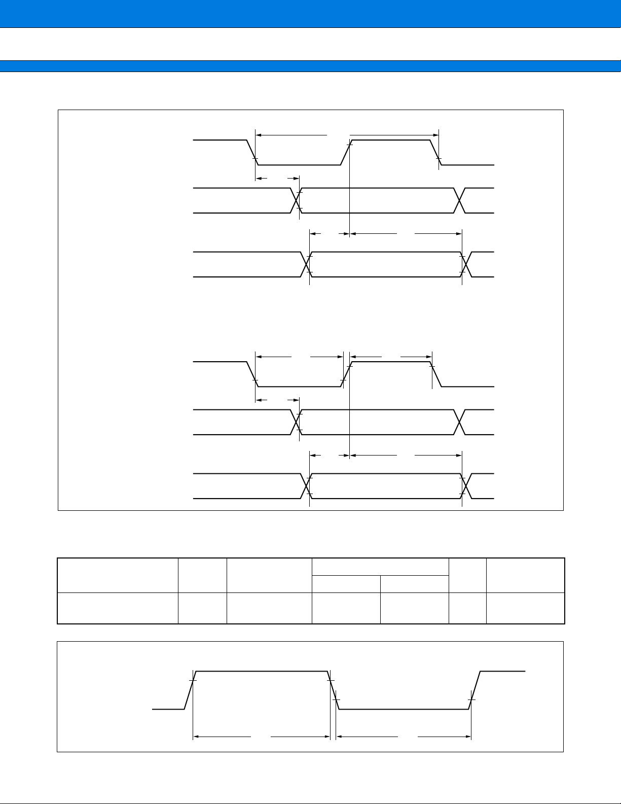
(5) Bus Read Timing
Parameter Symbol Pin name
(V
CC = 5.0 V±10%, VSS = AVSS = 0.0 V, TA = −40 °C to +85 °C)
Value
Unit Remarks
Min. Max.
ALE pulse width t
Effective address → ALE ↓ time t
ALE ↓ → address effective time t
Effective address → RD ↓ time tAVRL
Effective address → valid data
input
RD
pulse width tRLRH RD 3 tCP/2 − 20 — ns
LHLL ALE tCP/2 − 20 — ns
ALE, A23 to A16,
AVLL
AD15 to AD00
LLAX ALE, AD15 to AD00 tCP/2 − 15 — ns
A23 to A16,
AD15 to AD00, RD
AVDV
t
A23 to A16,
AD15 to AD00
tCP/2 − 20 — ns
tCP − 15 — ns
—5 tCP/2 − 60 ns
RD ↓ → valid data input tRLDV RD, AD15 to AD00 — 3 tCP/2 − 60 ns
RD
↑ → data hold time tRHDX RD, AD15 to AD00 0 — ns
RD
↑ → ALE ↑ time tRHLH RD, ALE tCP/2 − 15 — ns
RD ↑ → address effective time tRHAX ALE, A23 to A16 tCP/2 − 10 — ns
Effective address → CLK ↑ time t
RD
↓ → CLK ↑ time tRLCH RD, CLK tCP/2 − 20 — ns
ALE ↓ → RD
↓ time tLLRL ALE, RD tCP/2 − 15 — ns
AVCH
A23 to A16,
AD15 to AD00, CLK
tCP/2 − 20 — ns
•Bus read timing
CLK
ALE
RD
• Multiplex mode
A23 to A16
AD15 to AD00
tAVCH
2.4 V
2.4 V 2.4 V 2.4 V
tLHLL
tAVLL tRLRH
2.4 V
0.8 V
2.4 V
0.8 V
Address
0.8 V
tLLAX
tLLRL
tAVDV
2.4 V
0.8 V
tRLCH
0.8 V
tRLDVtAVRL
2.4 V
0.7 VCC
0.3 VCC
Read data
2.4 V
tRHLH
tRHAX
2.4 V
0.8 V
0.7 V
0.3 VCC
tRHDX
CC
38

(6) Bus Write Timing
Parameter
(V
CC = 5.0 V±10%, VSS = AVSS = 0.0 V, TA = −40 °C to +85 °C)
Symbol Pin name
MB90550A/550B Series
Value
Min. Max.
Unit
Remarks
Effective address → WR
WR
pulse width tWL WH WRH, WRL 3 tCP/2 – 20 — ns
valid data output→ WR
↓ time tAVWL
↑ time tDVWH
WR ↑ → data hold time tWHDX
WR
↑ → address effective time tWHAX
WR
↑ → ALE ↑ time tWHLH WRH, WRL, ALE tCP/2 – 15 — ns
A23 to A16, AD15 to
AD00, WR
H, WRL
AD15 to AD00,
WR
H, WRL
AD15 to AD00,
WR
H, WRL
A23 to A16,
WR
H, WRL
tCP – 15 — ns
3 tCP/2 – 20 — ns
20 — ns
tCP/2 – 10 — ns
WR ↓ → CLK ↑ time tWLCH WRH, WRL, CLK tCP/2 – 20 — ns
• Bus write timing
tWLCH
2.4 V
CLK
Multiplex
mode
tWHLH
2.4 V
ALE
WR
(WRL, WRH)
• Multiplex mode
A23 to A16
AD15 to AD00
2.4 V
0.8 V
2.4 V
0.8 V
tWLWHtAVWL
0.8 V
tDVWH
Address Write data
2.4 V
0.8 V
2.4 V
tWHAX
2.4 V
0.8 V
tWHDX
2.4 V
0.8 V
39

MB90550A/550B Series
(7) Ready Input Timing
Parameter Symbol Pin name
(V
CC = 5.0 V±10%, VSS = AVSS = 0.0 V, TA = −40 °C to +85 °C)
Value
Unit Remarks
Min. Max.
RDY setup time t
RDY hold time t
RYHS
RYHH 0—ns
RDY
CLK
45 — ns
Note : Use the automatic ready function when the setup time for the rising edge of the RDY signal is not sufficient.
• Ready input timing
CLK
ALE
WR
(WRL, WRH)
RDY
wait not
inserted
0.8 V
2.4 V
0.8 V
tRYHS tRYHH
CC
0.8 VCC
40
RDY
wait inserted
(1 cycle)
0.2 VCC

(8) Hold Timing
MB90550A/550B Series
(V
CC = 5.0 V±10%, VSS = AVSS = 0.0 V, TA = −40 °C to +85 °C)
Parameter Symbol Pin name
Value
Unit Remarks
Min. Max.
Pins in floating status → HAK
↓ time tXHAL
30 tCP ns
HAK
HAK
↑ → pin valid time tHAHV tCP 2 tCP ns
Note : More than 1 machine cycle is needed before HAK
changes after HRQ pin is fetched.
• Hold timing
HAK
tXHAL
Pins
High impedance
tHAHV
(9) UART, Extended I/O Serial 0, 1 Timing
(V
CC = 5.0 V±10%, VSS = AVSS = 0.0 V, TA = −40 °C to +85 °C)
Parameter
Symbol Pin name Condition
Min. Max.
Serial clock cycle time t
SCYC SCK0 to SCK2
8 t
Value
Unit Remarks
CP —ns
SCK ↓ → SOT delay time t
Valid SIN → SCK ↑ t
SLOV
IVSH
SCK0 to SCK2,
SOT0 to SOT2
SCK0 to SCK2,
SIN0 to SIN2
Internal shift clock
mode
C
+ 1 TTL for an output pin
SCK ↑ → valid SIN hold time t
Serial clock “H” pulse width t
Serial clock “L” pulse width t
SHSL SCK0 to SCK2
SLSH SCK0 to SCK2 4 tCP —ns
SCK ↓ → SOT delay time tSLOV
Valid SIN → SCK ↑ t
SCK ↑ → valid SIN hold time t
SCK0 to SCK2,
SHIX
SIN0 to SIN2
SCK0 to SCK2,
SOT0 to SOT2
SCK0 to SCK2,
IVSH
SIN0 to SIN2
SCK0 to SCK2,
SHIX
SIN0 to SIN2
External shift clock
mode
C
+ 1 TTL for an
output pin
Notes: • These are AC ratings in the CLK synchronous mode.
•C
L is the load capacitance value connected to pins while testing.
L = 80 pF
L = 80 pF
–80 80 ns
100 — ns
tCP —ns
4 t
CP —ns
— 150 ns
60 — ns
60 — ns
41
MB90550A/550B Series
• Internal shift clock mode
SCK
0.8 V 0.8 V
tSLOV
SOT
SIN
• External shift clock mode
tSCYC
2.4 V
2.4 V
0.8 V
tIVSH tSHIX
0.8 V
CC
0.2 VCC
0.8 VCC
0.2 VCC
SCK
SOT
SIN
(10) Timer Input Timing
Parameter
Input pulse width
0.2 VCC 0.2 VCC
tSLOV
Symbol Pin name
t
TIWH
tTIWL
TIN0, TIN1
IN0 to IN3
tSLSH tSHSL
0.8 VCC 0.8 VCC
2.4 V
0.8 V
tIVSH tSHIX
0.8 V
CC
0.2 VCC
CC = 5.0 V±10%, VSS = AVSS = 0.0 V, TA = −40 °C to +85 °C)
(V
0.8 VCC
0.2 VCC
Value
Unit Remarks
Min. Max.
4 tCP —ns
• Timer input timing
42
TIN0 to TIN1
IN0 to IN3
0.8 VCC 0.8 VCC
0.2 VCC 0.2 VCC
tTIWH tTIWL
(11) Timer Output Timing
Parameter Symbol Pin name
MB90550A/550B Series
(V
CC = 5.0 V±10%, VSS = AVSS = 0.0 V, TA = −40 °C to +85 °C)
Value
Min. Max.
Unit Remarks
CLK ↑ → T
OUT transition time tTO
• Timer output timing
(12) Trigger Input Timing
Parameter Symbol Pin name
CLK
TOT0,TOT1
OUT0,OUT1
PPG0 to PPG5
TOT0,TOT1,OUT0,
OUT1,PPG0 to PPG5
2.4 V
t
TO
2.4 V
0.8 V
(V
CC = 5.0 V±10%, VSS = AVSS = 0.0 V, TA = −40 °C to +85 °C)
Min. Max.
30 — ns
Value
Unit Remarks
Input pulse width t
• Trigger input timing
IRQ0 to IRQ7
TRGL IRQ0 to IRQ7 5 tCP —ns
0.8 VCC
tTRGH tTRGL
0.8 VCC
0.2 VCC 0.2 VCC
43

MB90550A/550B Series
2
C Interface
(13) I
(V
CC = 5.0 V±10%, VSS = AVSS = 0.0 V, TA = −40 °C to +85 °C)
Parameter Symbol Pin name
Min. Max.
Internal clock cycle time
Start condition output
Stop condition output
t
CP — 6 2.5 666 ns All products
t
STAO
t
STOO
SDA0 to SDA2
t
CP × m × n/2 – 20 tCP × m × n/2 + 20 ns
tCP (m × n/2 + 4)
– 20
SCL0 toSCL2
Start condition detection t
Stop condition detection
SCL output “L” width
SCL output “H” width
SDA output delay time
Setup after SDA output
interrupt period
SCL input “L” width t
STAI 3 tCP + 40 — ns
t
STOI 3 tCP + 40 — ns
t
tLOWO
SCL0 to SCL2
t
HIGHO
t
DOO
t
DOSUO 4 tCP – 20 — ns
LOWI
SDA0 to SDA2
SCL0 to SCL2
CP × m × n/2 – 20 tCP × m × n/2 + 20 ns
tCP (m × n/2 + 4)
– 20
2 t
CP – 20 2 tCP + 20 ns
CP + 40 — ns
3 t
SCL0 to SCL2
SCL input “H” width tHIGHI tCP + 40 — ns
SDA input setup time
SDA input hold time
t
SUI
SDA0 to SDA2
t
HOI 0—ns
SCL0 to SCL2
40 — ns
Value
tCP (m × n/2 + 4)
+ 20
tCP (m × n/2 + 4)
+ 20
Unit Remarks
Only as master
ns
Only as slave
Only as master
ns
Notes: • “m” and“n” in the above table represent the v alues of shift cloc k frequency setting bits (CS4 to CS0) in the
clock control register “ICCR”. For details, refer to the register description in the hardware manual.
•t
DOSUO represents the minimum value when the interrupt period is equal to or greater than the SCL “L” width.
• The SDA and SCL output values indicate that that rise time is 0 ns.
44

•I2C interface [data transmitter (master/slave)]
MB90550A/550B Series
tLOWO
SCL
tSTAO tDOOtDOO
SDA
2
C interface [data receiver (master/slave)]
•I
SCL
SDA
0.2 VCC
0.8 VCC 0.8 VCC 0.8 VCC
t
SUI
tHIGHO
0.8 VCC
189
tHIGHI tLOWI
7689
0.8 VCC 0.8 VCC
0.2 VCC
tSUI tHOI tDOSUO
ACK
0.2 VCC 0.2 VCC 0.2 VCC 0.2 VCC
tHOI tDOO tDOO tDOSUO
ACK
0.8 V
CC 0.8 VCC
tSTOI
45

MB90550A/550B Series
5. A/D Converter
Electrical Characteristics
(1)
(4.5 V ≤ AVRH − AVRL, VCC = AVCC = 5.0 V±10%, VSS = AVSS = 0.0 V, TA = −40 °C to +85 °C)
Parameter Symbol Pin name
Min. Typ. Max.
Resolution — — — 10 — bit
Total error — — — — ±5.0 LSB
Non-linearity error — — — — ±2.5 LSB
Differential linearity error — — — — ±1.9 LSB
Zero transition voltage V
Full-scale transition
voltage
OT AN0 to AN7
V
FST AN0 to AN7
AVRL−
3.5LSB
AVRH−
6.5LSB
Sampling period t SMP — 64 — 4096
Value
AVRL+
0.5LSB
AVRH−
1.5LSB
Unit Remarks
AVRL+
4.5LSB
AVRH+
1.5LSB
V
1LSB=
(AVRH−AVRL)
/1024
V
tCP
Compare time
A/D Conversion time t
tCMP —22——
CNV — 26.3 — —
Analog port input current IAIN AN0 to AN7 — — 10
Analog input voltage VAIN AN0 to AN7 AVRL — AVRH
— AVRH AVRL — AV
CC
µs
µs
µA
V
V
*1
*2
Reference voltage
V
mA
Power supply current
— AVRL 0 — AVRH
I
A
—3.57.0
AVCC
IAH ——5µA*3
Reference voltage
supply current
R
I
AVRH
IRH ——5µA*3
— 300 500
Offset between channels — AN0 to AN7 — — 4
*1:When F
*2: Equivalent to the time for conversion per channel if “t
CP = 8 MHz, tCMP = 176 × tCP. When FCP = 16 MHz, tCMP = 352 × tCP.
SMP = 64 × tCP” or “tCMP = 352 × tCP” is selected when FCP =
µA
LSB
16 MHz.
*3: Specifies the power-supply current (Vcc = AVcc = AVRH = 5.0 V) when the A/D converter is inactive and the
CPU has been stopped.
Notes: • The error becomes larger relatively as |AVRH-AVRL| becomes smaller.
• Use the output impedance r
External circuit output impedance r
S of the external circuit for analog input under the following condition:
S = 10 kΩ Max.
• If the output impedance of the external circuit is too high, the analog voltage sampling time may be
insufficient.
• If you insert a DC-blocking capacitor between the e xternal circuit and the input pin, select a capacitance
that is about several thousands times the sampling capacitance C
capacity potential division with C
SH.
SH in the chip to suppress the effect of
46

MB90550A/550B Series
• Analog input circuit model
Microcontroller internal circuit
Input pin AN0
rS
RSH
CSH
Comparator
Input pin AN7
VS
External circuit
to
S/H circuit
Analog channel selector
<Recommended/reference values for device parameters>
r
S = 10 kΩ or less
SH = About 3 kΩ
R
C
SH = About 25 pF
Note: Device parameter values are provided as reference values for design purposes; they
are not guaranteed.
47

MB90550A/550B Series
(2) Definitions of Terms
• Resolution: Analog transition identifiable by the A/D converter.
Analog voltage can be divided into 1024 (2
• Total error: Difference between actual and logical values. This error is the sum of an offset error, gain error,
non-linearity error and an error caused by noise.
• Linearity error: Deviation of the straight line drawn between the zero transition point (00 0000 0000 <-> 00
0000 0001) and the full-scale transition point (11 1111 1110 <-> 11 1111 1111) of the device
from actual conversion characteristics
• Differential linearity error: Deviation from the ideal input voltage required to shift output code by one LSB
• 10-bit A/D converter conversion characteristics
11 1111 1111
11 1111 1110
11 1111 1101
11 1111 1100
10
) components at 10-bit resolution.
•
•
•
•
•
•
•
Digital output
•
•
•
•
•
•
00 0000 0011
00 0000 0010
00 0000 0001
00 0000 0000
1LSB × N + VOT
VOT VNT VFSTV(N + 1)T
Analog input
V
1LSB =
Linearity error =
Differential linearity error =
FST − VOT
1022
V
NT − (1LSB × N + VOT)
V (
N + 1) T − VNT
1LSB
1LSB
Linearity error
[ LSB ]
− 1 [ LSB ]
48

EXAMPLE CHARACTERISTICS
■■■■
MB90550A/550B Series
1. “L”
level output voltage
700
600
500
400
300
VOL (mV)
200
100
0
0246810
VOL − IOL
Other than P20 to P27
I
OL (mA)
700
A = 25 °C
T
600
500
400
VOL (mV)
300
200
100
0
0 5 10 15
V
OL − IOL
P20 to P27
I
OL (mA)
VCC = 3.5 V
VCC = 4.0 V
VCC = 5.0 V
VCC = 6.0 V
20 25 30
49

MB90550A/550B Series
2. “H”
level output voltage
700
A = 25 °C
T
600
500
400
300
VCC − VOH (mV)
200
100
0
0 −2 −4 −6 −8 −10
(VCC − VOH) − IOH
Other than P50 to P55
I
OH (mA)
VCC = 3.5 V
V
CC = 4.0 V
V
CC = 5.0 V
VCC = 6.0 V
3. “H”
level input voltage / “L” level input voltage (CMOS input)
VIH / VIL − VCC
5
TA = 25 °C
4.5
4
3.5
3
2.5
VIH/VIL (V)
2
1.5
1
1.5
0
3.5 4 4.5 5 5.5
V
CC (V)
50

MB90550A/550B Series
4. “H”
level input voltage / “L” level input voltage (CMOS hysteresis input
VIHS / VILS − VCC
5
TA = 25 °C
4.5
4
3.5
3
2.5
2
VIHS/VILS (V)
1.5
1
1.5
0
3.5 4 4.5 5 5.5
VCC (V)
VIHS
V
IHL
)
51

MB90550A/550B Series
5. Power supply current
(fCP = internal operating clock frequency)
• MB90552A
• Measurement conditions: External clock mode, ROM read loop operation,
without resource operation, Typ. sample,
internal operating frequency = 4MHz (external rectangular wave
clock at 8MHz), T
30
A = 25 °C
T
25
A = 25 °C
ICC − VCC
fCP = 16 MHz
20
15
ICC (mA)
10
5
0
3.5 4 4.5 5 5.5
V
CC (V)
fCP = 10.6 MHz
fCP = 8 MHz
f
CP = 4 MHz
ICCS − VCC
10
A = 25 °C
T
9
8
7
6
5
ICCS (mA)
4
3
2
1
0
3.5 4 4.5 5 5.5
V
CC (V)
fCP = 16 MHz
fCP = 10.6 MHz
fCP = 8 MHz
fCP = 4 MHz
52

MB90550A/550B Series
• MB90F553A
• Measurement conditions: External clock mode, ROM read loop operation,
without resource operation, Typ. sample,
internal operating frequency = 4MHz (external rectangular wave
70
60
A = 25 °C
T
clock at 8MHz), T
A = 25 °C
ICC − VCC
50
40
ICC (mA)
30
20
10
4.5 5 5.5
fCP = 16 MHz
fCP = 10 MHz
fCP = 4 MHz
V
CC (V)
ICCS − VCC
12
T
A = 25 °C
10
f
CP = 16 MHz
8
6
ICCS (mA)
4
fCP = 10 MHz
f
V
CC (V)
CP = 4MHz
2
0
4.5 5 5.5
53

MB90550A/550B Series
6. Pull-up resistance
Pull-up resistance − VCC
90
80
70
60
50
40
30
Pull-up resistance (kΩ)
20
10
4 4.5 5 5.5
T
A = 25 °C
T
A = −40 °C
TA = 85 °C
V
CC (V)
54

ORDERING INFORMATION
■■■■
Part number Package Remarks
MB90552APF
MB90552BPF
MB90553APF
MB90553BPF
MB90T552APF
MB90T553APF
MB90F553APF
MB90P553APF
MB90552APFV
MB90552BPFV
MB90553APFV
MB90553BPFV
MB90T552APFV
MB90T553APFV
MB90F553APFV
MB90P553APFV
MB90550A/550B Series
100-pin plastic QFP
(FPT-100P-M06)
100-pin plastic LQFP
(FPT-100P-M05)
55

MB90550A/550B Series
PACKAGE DIMENSIONS
■■■■
100-pin plastic QFP
(FPT-100P-M06)
23.90±0.40(.941±.016)
20.00±0.20(.787±.008)
81
INDEX
100
LEAD No.
C
2000 FUJITSU LIMITED F100008-3C-3
1
0.65(.0256)TYP 0.30±0.10
18.85(.742)REF
22.30±0.40(.878±.016)
(.012±.004)
0.10(.004)
"A"
0.13(.005)
5180
50
(.551±.008) (.705±.016)
31
30
M
Details of "A" part
"B"
17.90±0.4014.00±0.20
0.18(.007)MAX
0.53(.021)MAX
0.25(.010)
0.30(.012)
3.35(.132)MAX
(Mounting height)
0.05(.002)MIN
(STAND OFF)
12.35(.486)
0.15±0.05(.006±.002)
Details of "B" part
REF
16.30±0.40
(.642±.016)
0 10°
0.80±0.20
(.031±.008)
Dimensions in mm (inches)
(Continued)
56

(Continued)
100-pin plastic LQFP
(FPT-100P-M05)
76 50
100
MB90550A/550B Series
16.00±0.20(.630±.008)SQ
14.00±0.10(.551±.004)SQ
75
INDEX
125
0.50(.020)
0.20±0.05
(.008±.002)
51
0.08(.003)
0.08(.003)
26
"A"
M
0.145±0.055
(.0057±.0022)
Details of "A" part
+0.20
.059 –.004
–0.10
1.50
(Mounting height)
0°~8°
0.50±0.20
(.020±.008)
0.60±0.15
(.024±.006)
+.008
0.10±0.10
(.004±.004)
(Stand off)
0.25(.010)
C
2000 FUJITSU LIMITED F100007S-3c-5
Dimensions in mm (inches)
57

MB90550A/550B Series
FUJITSU LIMITED
For further information please contact:
Japan
FUJITSU LIMITED
Corporate Global Business Support Division
Electronic Devices
Shinjuku Dai-Ichi Seimei Bldg. 7-1,
Nishishinjuku 2-chome, Shinjuku-ku,
Tokyo 163-0721, Japan
Tel: +81-3-5322-3347
Fax: +81-3-5322-3386
http://edevice.fujitsu.com/
North and South America
FUJITSU MICROELECTRONICS, INC.
3545 North First Street,
San Jose, CA 95134-1804, U.S.A.
Tel: +1-408-922-9000
Fax: +1-408-922-9179
Customer Response Center
Mon. - Fri.: 7 am - 5 pm (PST)
Tel: +1-800-866-8608
Fax: +1-408-922-9179
http://www.fujitsumicro.com/
Europe
FUJITSU MICROELECTRONICS EUR OPE GmbH
Am Siebenstein 6-10,
D-63303 Dreieich-Buchschlag,
Germany
Tel: +49-6103-690-0
Fax: +49-6103-690-122
http://www.fujitsu-fme.com/
Asia Pacific
FUJITSU MICROELECTRONICS ASIA PTE. LTD.
#05-08, 151 Lorong Chuan,
New Tech Park,
Singapore 556741
Tel: +65-281-0770
Fax: +65-281-0220
http://www.fmap.com.sg/
Korea
FUJITSU MICROELECTRONICS K OREA LTD.
1702 KOSMO TOWER, 1002 Daechi-Dong,
Kangnam-Gu,Seoul 135-280
Korea
Tel: +82-2-3484-7100
Fax: +82-2-3484-7111
All Rights Reserved.
The contents of this document are subject to change without notice.
Customers are advised to consult with FUJITSU sales
representatives before ordering.
The information and circuit diagrams in this document are
presented as examples of semiconductor device applications, and
are not intended to be incorporated in devices for actual use. Also,
FUJITSU is unable to assume responsibility for infringement of
any patent rights or other rights of third parties arising from the use
of this information or circuit diagrams.
The contents of this document may not be reproduced or copied
without the permission of FUJITSU LIMITED.
FUJITSU semiconductor devices are intended for use in standard
applications (computers, office automation and other office
equipments, industrial, communications, and measurement
equipments, personal or household devices, etc.).
CAUTION:
Customers considering the use of our products in special
applications where failure or abnormal operation may directly
affect human lives or cause physical injury or property damage, or
where extremely high levels of reliability are demanded (such as
aerospace systems, atomic energy controls, sea floor repeaters,
vehicle operating controls, medical devices for life support, etc.)
are requested to consult with FUJITSU sales representatives before
such use. The company will not be responsible for damages arising
from such use without prior approval.
Any semiconductor devices have inherently a certain rate of failure.
You must protect against injury, damage or loss from such failures
by incorporating safety design measures into your facility and
equipment such as redundancy, fire protection, and prevention of
over-current levels and other abnormal operating conditions.
If any products described in this document represent goods or
technologies subject to certain restrictions on export under the
Foreign Exchange and Foreign Trade Control Law of Japan, the
prior authorization by Japanese government should be required for
export of those products from Japan.
F0101
FUJITSU LIMITED Printed in Japan
 Loading...