


查询MB90522供应商
FUJITSU SEMICONDUCTOR
DATA SHEET
DS07-13702-4E
16-bit Proprietary Microcontroller
CMOS
F2MC-16LX MB90520 Series
MB90522/523/F523/V520
DESCRIPTION
■
The MB90520 series is a general-purpose 16-bit microcontroller developed and designed by Fujitsu for process
control applications in consumer products that require high-speed real-time processing.
The instruction set of the F
instruction sets for high-level languages, extended addressing mode, enhanced multiplication/division
instructions, and enhanced bit manipulation instructions. The microcontroller has a 32-bit accumulator for
processing long word data.
The MB90520 series has peripheral resources of 8/10-bit A/D converter, 8-bit D/A converter, UART (SCI),
extended I/O serial interfaces 0 and 1, 8/16-bit up/down counter/timers 0 and 1, 8/16-bit PPG timers 0 and 1,
I/O timer (16-bit free-run timers 1 and 2, input captures 0 and 1 (ICU), output compares 0 and 1 (OCU)), and
an LCD controller/driver.
2
MC stands for FUJITSU Flexible Microcontroller, a registered trademark of FUJITSU LIMITED.
*:F
2
MC-16LX CPU core inherits AT architecture of the F2MC* family with additional
FEATURES
■
•Clock
Embedded PLL clock multiplication circuit
Operating clock (PLL clock) can be selected from divided-b y-2 of oscillation or one to four times the oscillation
(at oscillation of 4 MHz, 4 MHz to 16 MHz).
The system can be operated by a sub-clock (rated at 32.768 kHz).
Minimum instruction execution time: 62.5 ns (at oscillation of 4 MHz, four times the oscillation clock, operation
at V
CC of 5.0 V)
PACKAGES
■
120-pin Plastic LQFP
(FPT-120P-M05)
120-pin Plastic QFP
(FPT-120P-M13)
(Continued)

MB90520 Series
(Continued)
• Maximum memory space
16 Mbytes
• Instruction set optimized for controller applications
Rich data types (bit, byte, word, long word)
Rich addressing mode (23 types)
Enhanced signed multiplication/division instruction and RETI instruction functions
Enhanced precision calculation realized by 32-bit accumulator
• Instruction set designed for high level language (C) and multi-task operations
Adoption of system stack pointer
Enhanced pointer indirect instructions
Barrel shift instructions
• Program patch function (for two address pointers)
• Enhanced execution speed
4-byte instruction queue
• Enhanced interrupt function
8 levels, 34 factors
• Automatic data transmission function independent of CPU operation
Extended intelligent I/O service function (EI
• Embedded ROM size and types
Mask ROM: 64 kbytes/128 kbytes
Flash ROM: 128 kbytes
• Embedded RAM size
Mask ROM: 4 kbytes
Flash ROM: 4 kbytes
Evaluation product: 6 kbytes
• Low-power consumption (stand-by) mode
Sleep mode (mode in which CPU operating clock is stopped)
Stop mode (mode in which oscillation is stopped)
CPU intermittent operation mode
Hardware stand-by mode
Clock mode (mode in which other than sub-clock and timebase timer are stopped)
•Process
CMOS technology
• I/O port
General-purpose I/O ports (CMOS): 53 ports
General-purpose I/O ports (via pull-up resistors): 24 ports
General-purpose I/O ports (open-drain): 8 ports
Total: 85 ports
•Timer
Timebase timer/watchdog timer: 1 channel
8/16-bit PPG timers 0, 1: 8-bit × 2 channels or 16-bit × 1 channel
• 16-bit re-load timers 0, 1: 2 channels
2
OS): Up to 16 channels
(Continued)
2

MB90520 Series
(Continued)
• 16-bit I/O timer
16-bit free-run timers 1, 2: 2 channels
Input captures 0, 1 (ICU): Generates an interrupt request by latching a 16-bit free-run timer counter value upon
detection of an edge input to the pin.
Output compares 0, 1 (OCU): Generates an interrupt request and reverses the output le vel upon detection of a
match between the 16-bit free-run timer counter value and the compare setting
value.
8/16-bit up/down counter/timers 0, 1: 1 channel (8-bit × 2 channels)
• Extended I/O serial interfaces 0, 1: 1 channel
•UART (SCI)
With full-duplex double buffer
Clock asynchronized or clock synchronized transmission can be selectively used.
• DTP/external interrupt circuit (8 channels)
A module for starting extended intelligent I/O service (EI
by an external input.
• Wak e-up interrupt
Receives external interrupt requests and generates an interrupt request upon an “L” level input.
• Delayed interrupt generation module
Generates an interrupt request for switching tasks.
• 8/10-bit A/D converter (8 channels)
8/10-bit resolution can be selectively used.
Starting by an external trigger input.
Conversion time: minimum 15.0 µs (at machine clock frequency of 16 MHz, including sampling time)
• 8-bit D/A converter (based on the R-2R system)
8-bit resolution: 2 channels (independent)
Setup time: 12.5 µs
• Clock timer: 1 channel
• LCD controller/driver
A common driver and a segment driver that can directly drive the LCD (liquid crystal display) panel
• Clock output function
2
OS) and generating an external interrupt triggered
Note: Do not set external bus mode for the MB90520 series because it cannot be operated in this mode.
3

MB90520 Series
PRODUCT LINEUP
■
Part number
Item
Classification Mask ROM product Flash ROM product Evaluation product
ROM size 64 kbytes 128 kbytes None
RAM size 4 kbytes 6 kbytes
CPU functions
MB90522 MB90523 MB90F523 MB90V520
Number of instructions: 351
Instruction bit length: 8 bits, 16 bits
Instruction length: 1 byte to 7 bytes
Data bit length: 1 bit, 8 bits, 16 bits
Minimum execution time: 62.5 ns
(at machine clock frequency of 16 MHz)
Interrupt processing time: 1.5 µs
(at machine clock frequency of 16 MHz, minimum value)
Ports
UART (SCI)
8/10-bit A/D converter
8/16-bit PPG timers 0, 1
8/16-bit up/down counter/
timers 0, 1
General-purpose I/O ports (CMOS output): 53
General-purpose I/O ports (via pull-up resistor): 24
General-purpose I/O ports (N-ch open-drain output): 8
Total: 85
Clock synchronized transmission (62.5 kbps to 1 Mbps)
Clock asynchronized transmission (1202 bps to 9615 bps)
Transmission can be performed by bi-directional serial transmission or by
master/slave connection.
Conversion precision: 8/10-bit can be selectively used.
Number of inputs: 8
One-shot conversion mode (converts selected channel only once)
Scan conversion mode (converts two or more successive channels and can
program up to 8 channels.)
Continuous conversion mode (converts selected channel continuously)
Stop conversion mode (converts selected channel and stop operation repeatedly)
Number of channels: 1 (8-bit × 2 channels)
PPG operation of 8-bit or 16-bit
Pulse wave of given intervals and given duty ratios can be output.
Pulse interval: 62.5 ns to 1 µs (at machine clock frequency of 16 MHz)
Number of channels: 1 (8-bit × 2 channels)
Event input: 6 channels
8-bit up/down counter/timer used: 2 channels
8-bit re-load/compare function supported: 1 channel
16-bit
I/O timer
4
16-bit free-run
timers 1, 2
Number of channels: 2
Overflow interrupts
(Continued)

(Continued)
MB90520 Series
Part number
Item
Output
16-bit
I/O timer
DTP/external interrupt circuit
Wake-up intrrupt
Delayed interrupt generation
module
Extended I/O serial
interfaces 0, 1
Timebase timer
compares 0, 1
(OCU)
Input captures
0, 1 (ICU)
MB90523 MB90523 MB90F523 MB90V520
Number of channels: 8
Pin input factor: Match signal of compare register
Number of channels: 2
Rewriting register value upon pin input (rising, falling, or both edges)
Number of inputs: 8
Started by rising edge, falling edge, “H” level input, or “L” level input.
External interrupt circuit or extended intelligent I/O service (EI
Number of inputs: 8
Started by “L” level input.
Interrupt generation module for switching tasks
Used in real-time operating systems.
Clock synchronized transmission (3125 bps to 1 Mbps)
LSB first/MSB first
18-bit counter
Interrupt interval: 1.024 ms, 4.096 ms, 16.384 ms, 131.072 ms
(at oscillation of 4 MHz)
2
OS) can be used.
8-bit resolution
8-bit D/A converter
LCD controller/driver
Watchdog timer
Low-power consumption
(stand-by) mode
Process CMOS
Power supply voltage for
operation*
* :Varies with conditions such as the operating frequency. (See section “■ Electrical Characteristics.”)
Assurance for the MB90V520 is given only for operation with a tool at a power voltage of 3.0 V to 5.5 V, an
operating temperature of 0 to 55 degrees centigrade, and an operating frequency of 1 MHz to 16 MHz.
Reset generation interval: 3.58 ms, 14.33 ms, 57.23 ms, 458.75 ms
Sleep/stop/CPU intermittent operation/clock timer/hardware stand-by
Number of power supply pins for LCD drive: 4
3.0 V to 5.5 V 4.0 V to 5.5 V 3.0 V to 5.5 V
Number of channels: 2 channels
Based on R-2R system
Number of common output pins: 4
Number of segment output pins: 32
RAM for LCD indication: 16 bytes
Booster for LCD drive: Internal
Split resistor for LCD drive: Internal
(at oscillation of 4 MHz, minimum value)
5

MB90520 Series
PACKAGE AND CORRESPONDING PRODUCTS
■
Package MB90522 MB90523 MB90F523
FPT-120P-M05
FPT-120P-M13
: Available × : Not available
Note: For more information about each package, see section “■ Package Dimensions.”
DIFFERENCES AMONG PRODUCTS
■
Memory Size
In evaluation with an evaluation chip, note the difference between the evaluation chip and the chip actually used.
The following items must be taken into consideration.
• The MB90V520 does not have an internal ROM. How ev er , operations equivalent to those perf ormed by a chip
with an internal ROM can be evaluated by using a dedicated development tool, enabling selection of ROM
size by setting the development tool.
• In the MB90V520, images from FF4000
mapped to bank FE and FF only. (This setting can be changed by configuring the development tool.)
• In the MB90522, images from FF4000
FF only.
• In the MB90523/F523, images from FF4000H to FFFFFFH are mapped to bank 00, and FE0000H to FF3FFFH
to bank FE and bank FF.
H to FFFFFFH are mapped to bank 00, and FE0000H to FF3FFFH are
H to FFFFFFH are mapped to bank 00, and FF0000H to FF3FFFH to bank
6

PIN ASSIGNMENT
■
MB90520 Series
(Top view)
P31/CKOT
P32/OUT0
P33/OUT1
P34/OUT2
P35/OUT3
P36/PG00
P37/PG01
CC
V
P40/PG10
P41/PG11
P42/SIN0
P43/SOT0
P44/SCK0
P45/SIN1
P46/SOT1
P47/SCK1
SEG00
SEG01
SEG02
SEG03
SEG04
SEG05
SEG06
SEG07
PA0/SEG08
PA1/SEG09
PA2/SEG10
PA3/SEG11
PA4/SEG12
PA5/SEG13
P30
VSSP27/ADTG
P26/ZIN0/INT7
P25/BIN0
P24/AIN0
P23/IC11
P22/IC10
P21/IC01
P20/IC00
P17/WI7
P16/WI6
P15/WI5
P14/WI4
P13/WI3
P12/WI2
P11/WI1
P10/WI0
P07
P06/INT6
P05/INT5
P04/INT4
P03/INT3
P02/INT2
120
119
118
117
116
115
114
113
112
111
110
109
108
107
106
105
104
103
102
101
1
2
3
4
5
6
7
8
9
10
11
12
13
14
15
16
17
18
19
20
21
22
23
24
25
26
27
28
29
30
3132333435363738394041424344454647484950515253545556575859
1009998979695949392
P01/INT1
P00/INT0
VCCX1X0V
SS
91
60
90
89
88
87
86
85
84
83
82
81
80
79
78
77
76
75
74
73
72
71
70
69
68
67
66
65
64
63
62
61
RST
MD0
MD1
MD2
HST
V3
V2
V1
V0
P97/SEG31
P96/SEG30
P95/SEG29
P94/SEG28
P93/SEG27
P92/SEG26
P91/SEG25
X0A
X1A
P90/SEG24
P87/SEG23
P86/SEG22
P85/SEG21
P84/SEG20
P83/SEG19
P82/SEG18
P81/SEG17
P80/SEG16
SS
V
P77/COM3
P76/COM2
PA6/SEG14
PA7/SEG15
VSSC
P50/SIN2/AIN1
P51/SOT2/BIN1
P52/SCK2/ZIN1
DVCCDVSSP53/DA0
P54/DA1
AVCCAVRH
AVRL
(FPT-120P-M05)
(FPT-120P-M13)
AVSSP60/AN0
P61/AN1
P62/AN2
P63/AN3
P64/AN4
P65/AN5
P66/AN6
P67/AN7
VCCP70/TI0/OUT4
P71/TO0/OUT5
P72/TI1/OUT6
P73/TO1/OUT7
P74/COM0
P75/COM1
7

MB90520 Series
PIN DESCRIPTION
■
Pin no.
Pin name
LQFP-120*
QFP-120*
92,
74,
89 to 87 MD0 to MD2 C This is an input pin for selecting operation modes.
95 to 101 P00 to P06 D This is a general-purpose I/O port.
102 P07 D This is a general-purpose I/O port.
103 to 110 P10 to 17 D This is a general-purpose I/O port.
111,
112,
113,
114
115 P24 E This is a general-purpose I/O port.
116 P25 E This is a general-purpose I/O port.
1
2
X0,
93
73
90 RST C This is an external reset request signal input pin.
86 HST
X1
X0A,
X1A
INT0 to INT6 This is a request input pin of the DTP/external interrupt circuit ch.0
WI0 to WI7 This is an I/O pin for wake-up interrupts.
P20,
P21,
P22,
P23
IC00,
IC01,
IC10,
IC11
AIN0 This port can be used as count clock A input for 8/16-bit up/down
BIN0 This port can be used as count clock B input for 8/16-bit up/down
Circuit
type
A This is a high-speed crystal oscillator pin.
B This is a low-speed crystal oscillator pin.
Connect directly to V
C This is a hardware stand-by input pin.
This function can be set by the port 0 input pull-up resistor setup
register (RDR0) for input. For output, however, this function is
invalid.
to ch.6.
This function can be set by the port 0 input pull-up resistor setup
register (RDR0) for input. For output, however, this function is
invalid.
This function can be set by the port 1 input pull-up resistor setup
register (RDR1) for input. For output, however, this function is
invalid.
E This is a general-purpose I/O port.
This is a trigger input pin for input capture (ICU) 0 and 1.
Since this input is used as required for input capture 0 and 1 (ICU)
ch.0, ch.01, ch.10 and ch.11 input operation, output by other
functions must be suspended except for intentional operation.
counter/timer 0.
counter/timer 0.
CC or VSS.
Function
*1: FPT-120P-M05
*2: FPT-120P-M13
8
(Continued)

Pin no.
Pin name
LQFP-120*
QFP-120*
117 P26 E This is a general-purpose I/O port.
118 P27 E This is a general-purpose I/O port.
120 P30 E This is a general-purpose I/O port.
1
2
ZIN0 This port can be used as count clock Z input for 8/16-bit up/down
INT7 This is a request input pin of the DTP/external interrupt circuit
ADTG
1 P31 E This is a general-purpose I/O port.
CKOT This is a clock monitor function output pin.
2 P32 E This is a general-purpose I/O port.
OUT0 This is an event output pin for output compare 0 (OCU) ch.0.
3 P33 E This is a general-purpose I/O port.
OUT1 This is an event output pin for output compare 0 (OCU) ch.1.
4 P34 E This is a general-purpose I/O port.
OUT2 This is an event output pin for output compare 0 (OCU) ch.2.
5 P35 E This is a general-purpose I/O port.
OUT3 This is an event output pin for output compare 0 (OCU) ch.3.
6 P36 E This is a general-purpose I/O port.
PG00 This is an output pin of 8/16-bit PPG timer 0.
Circuit
type
counter/timer 0.
ch.7.
This is an external trigger input pin of the 8/10-bit A/D converter.
Since this input is used as required for 8/10-bit A/D conv erter input
operation, output by other functions must be suspended e xcept f or
intentional operation.
This function is valid when clock monitor output is enabled.
This function becomes valid when waveform output from the
OUT0 is disabled.
This function is valid when output for each channel is enabled.
This function becomes valid when waveform output from the
OUT1 is disabled.
This function is valid when output for each channel is enabled.
This function becomes valid when waveform output from the
OUT2 is disabled.
This function is valid when output for each channel is enabled.
This function becomes valid when waveform output from the
OUT3 is disabled.
This function is valid when output for each channel is enabled.
This function becomes valid when wa vef orm output from the PG00
is disabled.
This function becomes valid when waveform output from PG00 is
enabled.
MB90520 Series
Function
*1: FPT-120P-M05
*2: FPT-120P-M13
(Continued)
9

MB90520 Series
Pin no.
Pin name
LQFP-120*
QFP-120*
1
2
7 P37 E This is a general-purpose I/O port.
PG01 This is an output pin of 8/16-bit PPG timer 0.
9,
10
11 P42 D This is a general-purpose I/O port.
12 P43 D This is a general-purpose I/O port.
13 P44 D This is a general-purpose I/O port.
14 P45 D This is a general-purpose I/O port.
P40,
P41
PG10,
PG11
SIN0 This is a serial data input pin of UART (SCI).
SOT0 This is a serial data output pin of UART (SCI).
SCK0 This is a serial clock I/O pin of UART (SCI).
SIN1 This is a data input pin for extended I/O serial interface 0.
Circuit
type
This function becomes valid when wa vef orm output from the PG01
is disabled.
This function becomes valid when waveform output from PG01 is
enabled.
D This is a general-purpose I/O port.
This function becomes valid when wa vef orm output from the PG10
and PG11 are disabled.
This function can be set by the pull-up resistor setup register
(RDR4) for input. For output, however, this function is invalid.
This is an output pin of 8/16-bit PPG timer 1.
This function becomes valid when waveform outputs from PG10
and PG11 are enabled.
This function can be set by the pull-up resistor setup register
(RDR4) for input. For output, however, this function is invalid.
Because this input is used as required when UART (SCI) is
performing input operations, it is necessary to stop outputs by
other functions unless such outputs are made intentionally.
When using other output functions as well, disable output during
SIN operation.
This function can be set by the pull-up resistor setup register
(RDR4) for input. For output, however, this function is invalid.
This function becomes valid when serial data output from UART
(SCI) is enabled.
This function can be set by the pull-up resistor setup register
(RDR4) for input. For output, however, this function is invalid.
This function becomes valid when serial clock output from UART
(SCI) is enabled.
This function can be set by the port 4 input pull-up resistor setup
register (RDR4) for input. For output, however, this function is
invalid.
Since this input is used as required for serial data input operation,
output by other functions must be suspended e xcept for intentional
operation. When using other output functions as well, disable
output during SIN operation.
Function
*1: FPT-120P-M05
*2: FPT-120P-M13
10
(Continued)
Pin no.
Pin name
LQFP-120*
QFP-120*
40,
46 to 53 P60 to P67 K This is a general-purpose I/O port.
1
2
15 P46 D This is a general-purpose I/O port.
SOT1 This is a data output pin for extended I/O serial interface 0.
16 P47 D This is a general-purpose I/O port.
SCK1 This is a serial clock I/O pin for extended I/O serial interface 0.
35 P50 D This is a general-purpose I/O port.
SIN2 This is a data input pin for extended I/O serial interface 1.
AIN1 This port can be used as count clock A input for 8/16-bit up/down
36 P51 D This is a general-purpose I/O port.
SOT2 This is a data output pin for extended I/O serial interface 1.
BIN1 This port can be used as count clock B input for 8/16-bit up/down
37 P52 D This is a general-purpose I/O port.
SCK2 This is a serial clock I/O pin for extended I/O serial interface 1.
ZIN1 This port can be used as control clock Z input for 8/16-bit up/do wn
P53,
41
P54
DA0,
DA1
AN0 to AN7 These are analog input pins of the 8/10-bit A/D converter.
Circuit
type
This function can be set by the port 4 input pull-up resistor setup
register (RDR4) for input. For output, however, this function is
invalid.
This function becomes valid when serial data output from SOT1 is
enabled.
This function can be set by the port 4 input pull-up resistor setup
register (RDR4) for input. For output, however, this function is
invalid.
This function becomes valid when serial clock output from SCK1 is
enabled.
Since this input is used as required for serial data input operation,
output by other functions must be suspended e xcept for intentional
operation.
counter/timer 1.
This function becomes valid when serial data output from SOT2 is
enabled.
counter/timer 1.
This function becomes valid when serial clock output from serial
SCK2 is enabled.
counter/timer 1.
I This is a general-purpose I/O port.
These are analog signal output pins for 8-bit D/A converter ch.0
and ch.1.
The input function become valid when the analog input enable
register (ADER) is set to select a port.
This function is valid when the analog input enable register
(ADER) is enabled.
Function
MB90520 Series
*1: FPT-120P-M05
*2: FPT-120P-M13
(Continued)
11

MB90520 Series
Pin no.
Pin name
57
58
1
2
P70,
P72
TI0,
TI1
OUT4,
OUT6
P71,
P73
LQFP-120*
QFP-120*
55,
56,
Circuit
type
E This is a general-purpose I/O port.
These are event input pins for 16-bit re-load timers 0 and 1.
Since this input is used as required for 16-bit re-load timers 0 and
1 operation, output by other functions must be suspended except
for intentional operation.
These are event output pins for output compare 1 (OCU) ch.4 and
ch.6.
This function is valid when output for each channel is enabled.
E This is a general-purpose I/O port.
This function is valid when TO0 and TO1 output are disabled.
Function
TO0,
TO1
OUT5,
OUT7
These are output pins for 16-bit re-load timers 0 and 1.
This function is valid when TO0 and TO1 output are enabled.
These are event output pins for output compare 1 (OCU) ch.5 and
ch.7.
This function is valid when output for each channel is enabled.
59 to 62 P74 to P77 L This is a general-purpose I/O port.
This function is valid with port output specified for the LCD
controller/driver control register.
COM0 to
COM3
These are common pins for the LCD controller/driver.
This function is valid with common output specified for the LCD
controller/driver control register.
64 to 71 P80 to P87 L This is a general-purpose I/O port.
This function is valid with port output specified for the LCD
controller/driver control register.
SEG16 to
SEG23
These are segment outputs for the LCD controller/driver.
This function is valid with segment output specified for the LCD
controller/driver control register.
72,
75 to 81
P90,
P91 to P97
M This is a general-purpose I/O port.
The maximum I
OL can be 10mA.
This function is valid with port output specified for the LCD
controller/driver control register.
SEG24,
SEG25 to
SEG31
17 to 24 SEG00 to
SEG07
F These are pins dedicated to LCD segments 00 to 07 for the LCD
These are segment outputs for the LCD controller/driver.
This function is valid with port output specified for the LCD
controller/driver control register.
controller/driver.
25 to 32 PA0 to PA7 L This is a general-purpose I/O port.
This function is valid with port output specified for the LCD
controller/driver control register.
SEG08 to
SEG15
These are pins for LCD segments 08 to 15 for the LCD controller/
driver.
Units of four ports or segments can be selected by the internal
register in the LCD controller.
*1: FPT-120P-M05
*2: FPT-120P-M13
(Continued)
12

MB90520 Series
(Continued)
Pin no.
1
LQFP-120*
QFP-120*
Pin name
2
34 C G This is a capacitance pin for power supply stabilization.
82 to 85 V0 to V3 N This is a pin for the reference power supply for the LCD controller/
8,
V
CC Power
54,
94
33,
V
SS Power
63,
91,
119
42 AV
CC H This is a power supply for the analog circuit.
43 AVRH J This is a reference v oltage input to the analog circuit.
44 AVRL H This is a reference voltage input to the analog circuit.
45 AV
38 DV
39 DV
SS H This is a GND level of the analog circuit.
CC H This is the Vref input pin for the D/A converter.
SS H This is the GND level pin for the D/A converter.
Circuit
type
supply
supply
Function
Connect an external ceramic capacitor rated at about 0.1 µF. This
capacitor is not, however, required for the M90F523 (flash
product).
driver.
This is a power supply (5.0 V) input pin to the digital circuit.
This provides the GND level (0.0 V) input pin for the digital circuit.
Make sure to turn on/turn off this power supply with a voltage
exceeding AV
CC applied to VCC.
Make sure to turn on/turn off this power supply with a voltage
exceeding AVRH applied to AV
The voltage to be applied must not exceed V
The potential must be the same as V
CC.
CC.
SS.
*1: FPT-120P-M05
*2: FPT-120P-M13
13

MB90520 Series
I/O CIRCUIT TYPE
■
Type Circuit Remarks
A • High-speed oscillation feedback resistor
X1
approx. 1MΩ
X0
Nch
Pch
Pch
Nch
Standby control signal
B • Low-speed oscillation feedback resistor
X1A
X0A
Nch
Pch
Pch
Nch
Standby control signal
approx. 1MΩ
C • Hysteresis input
R
Hysteresis input
14
D • Hysteresis input (can be set with the input
Pch
Pch
Selecting signal
with or without a
input pull-up resistor
pull-up resistor)
CMOS level output
• Pull-up resistor approx. 50 kΩ
• Provided with a standby control function
I
OL = 4 mA
Nch
R
Hysteresis input
Standby control for
input interruption
for input interruption
(Continued)
MB90520 Series
Type Circuit Remarks
E • CMOS hysteresis input/output
Pch
R
IOL = 4 mA
F • Pins dedicated to segment output
CC
V
Nch
Hysteresis input
Standby control for input interruption
• CMOS level output
• Provided with a standby control function
for input interruption
Pch
Nch
R
G • C pin output
(Pin for capacitor connection)
Pch
Nch
N.C. pin for the MB90F523
H • Analog power input protector
Pch
AVP
Nch
I • CMOS hysteresis input/output
• Pin for analog output/CMOS output
(During analog output, CMOS output is
not produced.)
Pch
CC
V
(Analog output has priority over CMOS
Nch
output: DAE = 1)
• Provided with a standby control function
I
OL = 4 mA
R
Hysteresis input
Standby control for input interruption
DAO
for input interruption
(Continued)
15

MB90520 Series
Type Circuit Remarks
J • Input pin for ref+ power for the A/D
Pch
Nch
Pch
Nch
ANE
AVR
ANE
K • Hysteresis input/analog input
Pch
Nch
converter
Provided with power protection
• CMOS output
• Provided with a standby control for input
interruption
I
OL = 4 mA
R
Standby control for input interruption
Hysteresis input
Analog input
L • CMOS hysteresis input/output
Pch
• Segment input
• Standby control to cut off the input is
available in segment input operation
Nch
R
Standby control for input interruption
IOL = 4 mA
Hysteresis input
SEG
M • Hysteresis input
Nch
• Nch open-drain output
(High current for LCD drive)
• Standby control to cut off the input is
R
IOL = 10 mA
Nch
Hysteresis input
Standby control for input interruption
available in segment input operation
16
N • Reference power supply pin for the LCD
controller
IOL = 10 mA
Pch
Nch
R

MB90520 Series
HANDLING DEVICES
■
1. Ensuring that the Voltage does not exceed the Maximum Rating (to Avoid a Latch-up).
In CMOS ICs, a latch-up phenomenon is caused when a voltage exceeding VCC or below VSS is applied to
input or output pins or if a voltage exceeding the rating is applied across VCC and VSS.
When a latch-up is caused, the power supply current may be dramatically increased, resulting in thermal
breakdown of devices. To avoid the latch-up, make sure that the voltage does not exceed the maximum rating.
In turning on/turning off the analog power supply, make sure the analog power voltages (AVCC, AVRH, DVCC)
and analog input voltages do not exceed the digital voltage (V
And also make sure the voltages applied to the LCD power supply pins (V3 to V0) do not exceed the power
supply voltage (V
CC).
2. Handling Unused Pins
• Unused input pins left open may cause abnormal operation, or latch-up leading to permanent damage. Unused
input pins should be pulled-up or pull-down through at least 2 kΩ resistance.
• Unused input/output pins may be left open in output state, but if such pins are in input state they should be
handled in the same way as input pins.
CC).
3. Notes on Using External Clock
In using the external clock, drive X0 pin only and leave X1 pin unconnected.
Using external cloc k
•
X0
Open
MB90520 series
X1
4. Unused Sub Clock Mode
If sub clock modes are not used, the oscillator should be connected to the X0A pin and X1A pin.
5. Power Supply Pins
In products with multiple Vcc or Vss pins, pins with the same potential are internally connected in the device to
avoid abnormal operations including latch-ups. However, the pins should be connected to external powers and
ground lines to lower the electro-magnetic emission level, to prevent abnormal operation of strobe signals caused
by the rise in the ground level, and to conform to the total current rating.
Make sure to connect V
It is recommended that a bypass capacitor of around 0.1 µF be placed between the V
device.
cc and Vss pins via lowest impedance to power lines.
cc and Vss pins near the
17

MB90520 Series
Using
•
power supply pins
V
CC
V
SS
V
CC
V
SS
V
SS
MB90520 series
V
CC
V
SS
V
CC
V
SS
V
CC
6. Crystal Oscillator Circuit
Noise around the X0 and X1 pins may cause abnormal operation in this device. In designing printed circuit
boards, the X0 and X1 pins and crystal oscillator (or ceramic oscillator), as well as the bypass capacitor to the
ground, should be placed as close as possible, and the related wiring should have as few crossings with other
wiring as possible.
Circuit board artwork in which the area of the X0 and X1 pins is surrounded by grounding is recommended for
stabilizing the operation.
7. Turning-on Sequence of Power Supply to A/D Converter and Analog Inputs
Make sure to turn on the A/D converter power supply, D/A converter power supply (AVCC, AVRH, AVRL, DVCC,
DVSS) and analog inputs (AN0 to AN7) after turning on the digital power supply (VCC).
Turn off the digital power after turning off the A/D converter supply and analog inputs. In this case, make sure
that AVRH and DV
acceptable).
CC do not exceed AVCC (turning on/off the analog and digital supplies simultaneously is
8. Connection of Unused Pins of A/D Converter
Connect unused pins of A/D converter and those of D/A converter to AVCC = DVCC = VCC, AVSS = AVRH = AVRL
= V
SS.
9. N.C. Pin
The N.C. (internally connected) pin must be opened for use.
10.Notes on Energization
To prevent the internal regulator circuit from malfunctioning, set the voltage rise time during energization at
50 µs or more (0.2 V to 2.7 V).
11.Use of SEG/COM Pins for the LCD Controller/Driver as Ports
In MB90520 series, pins SEG08 to SEG31, and COM0 to COM3 can also be used as general-purpose ports.
The electrical standard is such that pins SEG08 to SEG23, and COM0 to COM3 have the same ratings as the
CMOS output port, while pins SEG24 to SEG31 have the same ratings as the open-drain type.
18

MB90520 Series
12.
Indeterminate outputs from ports 0 and 1
The outputs from ports 0 and 1 become indeterminate during oscillation setting time of step-down circuit (during
a power-on reset) after the power is turned on.
Pay attention to the port output timing shown as follow
Timming chart of indeterminate outputs from ports o and 1
•
Oscillation setting time
∗2
Step-down circuit
setting time
∗1
Vcc(power-supply pin)
PONR(power-on reset) signal
(external asynchronous reset) signal
RST
RST(internal reset) signal
Oscillation clock signal
KA(internal operation clock A) signal
KB(internal operation clock B) signal
PORT(port output)signal
indereterminate period
* : 1:Step-down circuit setting time : 217/oscillation clock frequency (oscillation clock frequency of 16 MHz: 8.19 ms)
* :2:Oscillation setting time: 2
18
/oscillation clock frequency (oscillation cllock frequency of 16 MHz: 16.38 ms)
13.Initialization
The device contains internal registers that can be initialized only by a power-on reset. To initialize the internal
registers, restart the power supply.
14. Interrupt Recovery from Standby
If an external interrupt is used for recovery from standby, use an “H” level input request. An “L” level request
causes abnormal operation.
15.Precautions for Use of “DIV A, Ri”, and “DIVW A, Ri” Instructions
The signed multiplication-division instructions “DIV A, Ri”, and “DIVW A, RWi” should be used when the
corresponding bank registers (DTB, ADB, USB, SSB) are set to value “00h”. If the corresponding bank registers
(DTB, ADB, USB, SSB) are set to a value other than “00h,” then the remainder obtained after the execution of
the instruction will not be placed in the instruction operand register.
16.
Precautions for Use of REALOS
Extended intelligent I/O service(EI
2
OS) cannot be used, when REALOS is used.
19

MB90520 Series
BLOCK DIAGRAM
■
X0, X1
X0A, X1A
RST
HST
P07
P00/INT0 to P06/INT6
P24/AIN0
P25/BIN0
P26/ZIN0/INT7
P20/IC00
P21/IC01
P32/OUT0
P33/OUT1
P34/OUT2
P35/OUT3
P31/CKOT
P30
P36/PG00
P37/PG01
P40/PG10
P41/PG11
P42/SIN0
P43/SOT0
P44/SCK0
P45/SIN1
P46/SOT1
P47/SCK1
Oscillation clock
Sub clock
77
F2MC-16LX
CPU
Clock control
block*
(including
1
timebase timer)
2
Port 0*
DTP/
external
interrupt
circuit
4
Port 2*
8/16-bit
3
up/down
counter/timer
0, 1
16-bit
I/O timer 1
Input
2
capture 0
(ICU)
16-bit
free-run
timer 1
Output
4
compare 0
(OCU)
Clock output
4
Port 3*
2
8/16-bit
PPG
2
timer 0, 1
UART
(SCI)
SIO ch.0
2
Port 4*
Port 8*
LCD
controller/
driver
Port 7*
5
, 9*5, A*
24
4
8
5
4
P80/SEG16 to P87/SEG23
8
P90/SEG24 to P97/SEG31
8
PA0/SEG08 to PA7/SEG15
8
SEG00 to SEG07
4
V0 to V3
4
P74/COM0 to P77/COM3
16-bit
re-load
timer 0
16-bit
re-load
timer 1
16-bit
I/O timer 2
Output
compare
(OCU)
16-bit
free-run
timer 2
capture 1
Input
(ICU)
Port 2*
Port 6*
4
2
4
4
88
Intrnal data bus
8/10-bit
A/D
converter
P70/TI0/OUT4
P71/TO0/OUT5
P72/TI1/OUT6
P73/TO1/OUT7
P22/IC10
P23/IC11
P60/AN0 to P67/AN7
CC
AV
SS
AV
AVRH
AVRL
P27/ADTG
4
Port 2*
Interrupt controller
5
Port 5*
P50/SIN2/AIN1
SIO ch.1
P51/SOT2/BIN1
P52/SCK2/ZIN1
2
P10/WI0 to P17/WI7
Port 1*
88
Wake-up
interrupt
8-bit D/A
converter
× 2 ch.
2
P53/DA0
P54/DA1
DV
DV
Other pins
MD0 to MD2,
CC
SS
, V
C, V
RAM
ROM
Notes: Actually 16-bit free-run timer 1 is supported although two free-run timers are seemingly supported.
*1: The clock control circuit comprises a watchdog timer, a timebase timer, and a power consumption controller.
*2: A register for setting a pull-up resistor is supported.
*3: This is a high-current port for an LCD drive.
*4: A register for setting a pull-up resistor is supported. Signals in the CMOS level are input and output.
*5: Also used for LCD output. With this port used as is, Nch open-drain output develops . A register f or setting a pull-up resi stor
is supported.
20
CC
SS

MEMORY MAP
■
H
FFFFFF
Address #1
H
FE0000
H
010000
Address #2
H
004000
H
002000
Address #3
H
000100
H
0000C0
H
000000
Single chip mode
A mirroring function
is supported.
ROM area
ROM area
(image of
bank FF)
Register
RAM
Peripheral
MB90520 Series
Part number Address #1* Address #2 * Address #3 *
MB90522 FF0000
H 004000H 001100H
MB90523 FE0000H 004000H 001100H
MB90F523 FE0000H 004000H 001100H
: Internal access memory
: Access prohibited
*: Addresses #1, #2 and #3 vary with product type.
Note: The ROM data of bank FF is reflected in the upper address of bank 00, realizing effective use of the C
compiler small model. The lower 16-bit of bank FF and the lower 16-bit of bank 00 are assigned to the
same address, enabling reference of the table on the ROM without stating “far.”
For e xample, if an attempt has been made to access 00C000
H, the contents of the ROM at FFC000H are
actually accessed. Since the ROM area of the FF bank exceeds 48k bytes, the whole area cannot be
reflected in the image for the 00 bank. The ROM data at FF4000
were the image for 00400
the area of FF4000
H to 00FFFFH. Thus, it is recommended that the ROM data table be stored in
H to FFFFFFH.
H to FFFFFFH looks, therefore, as if it
21

MB90520 Series
2
F
MC-16LX CPU PROGRAMMING MODEL
■
• Dedicated registers
AH AL
USP
SSP
PS
PC
DPR
PCB
DTB
USB
: Accumlator (A)
Dual 16-bit register used for storing results of calculation, etc. The two 16-bit
registers can be combined to be used as a 32-bit register.
: User stack pointer (USP)
16-bit pointer for containing a user stack address.
: System stack pointer (SSP)
16-bit pointer for displaying the status of the system stack address.
: Processor status (PS)
16-bit register for displaying the system status.
: Program counter (PC)
16-bit register for displaying the storing location of the current instruction code.
: Direct page register (DPR)
8-bit register for specifying bit 8 through 15 of the operand address in the short
direct addressing mode.
: Program bank register (PCB)
8-bit register for displaying the program space.
: Data bank register (DTB)
8-bit register for displaying the data space.
: User stack bank register (USB)
8-bit register for displaying the user stack space.
32-bit
16-bit
SSB
ADB
8-bit
: System stack bank register (SSB)
8-bit register for displaying the system stack space.
: Additional data bank register (ADB)
8-bit register for displaying the additional data space.
22

• General-purpose registers
MB90520 Series
Maximum of 32 banks
H
000180
+ (RP × 10H )
• Processor status (PS)
ILM RP CCR
bit 15 bit 14 bit 13 bit 12 bit 11 bit 10 bit 9 bit 8 bit 7 bit 6 bit 5 bit 4 bit 3 bit 2 bit 1 bit 0
PS
ILM2 B4ILM1 ILM0 B3 B2 B1 B0 — I S T N Z V C
R7
R5
R3
R1
RW3
RW2
RW1
RW0
16-bit
R6
R4
R2
R0
RW7
RL3
RW6
RW5
RL2
RW4
RL1
RL0
Initial value
— : Unused
X : Indeterminate
00 000000 10XXXXX
—
23

MB90520 Series
I/O MAP
■
Address
000000
Abbreviated
register
Register name
name
H PDR0 Port 0 data register R/W Port 0 XX X XXXXX B
Read/
write
Resource name Initial value
000001H PDR1 Port 1 data register R/W Port 1 XX X XXXXX B
000002H PDR2 Port 2 data register R/W Port 2 XX X XXXXX B
000003H PDR3 Port 3 data register R/W Port 3 XX X XXXXX B
000004H PDR4 Port 4 data register R/W Port 4 XX X XXXXX B
000005H PDR5 Port 5 data register R/W Port 5 XX X XXXXX B
000006H PDR6 Port 6 data register R/W Port 6 XX X XXXXX B
000007H PDR7 Port 7 data register R/W Port 7 XX X XXXXX B
000008H PDR8 Port 8 data register R/W Port 8 XX X XXXXX B
000009H PDR9 Port 9 data register R/W Port 9 XX X XXXXX B
00000AH PDRA Port A data register R/W Port A XXXXX X X X B
00000BH LCDCMR Port 7/COM pin selection register R/W
00000CH
OCP4 OCU compare register ch.4 R/W
00000DH XXXXXXXXB
Port 7,
LCD controller/driver
16-bit I/O timer
(output compare 1
(OCU) section)
XXXX0 000B
XXXXXXXXB
00000EH (Disabled)
00000F
H EIFR Wake-up interrupt flag register R/W
Wake-up interrupt
XXXXXXX0 B
000010H DDR0 Port 0 direction register R/W Port 0 0 0 0 0 0 0 0 0 B
000011H DDR1 Port 1 direction register R/W Port 1 0 0 0 0 0 0 0 0 B
000012H DDR2 Port 2 direction register R/W Port 2 0 0 0 0 0 0 0 0 B
000013H DDR3 Port 3 direction register R/W Port 3 0 0 0 0 0 0 0 0 B
000014H DDR4 Port 4 direction register R/W Port 4 0 0 0 0 0 0 0 0 B
000015H DDR5 Port 5 direction register R/W Port 5 XXX 0 0 0 0 0 B
000016H DDR6 Port 6 direction register R/W Port 6 0 0 0 0 0 0 0 0 B
000017H DDR7 Port 7 direction register R/W Port 7 0 0 0 0 0 0 0 0 B
000018H DDR8 Port 8 direction register R/W Port 8 0 0 0 0 0 0 0 0 B
000019H DDR9 Port 9 direction register R/W Port 9 0 0 0 0 0 0 0 0 B
00001AH DDRA Port A direction register R/W Port A 0 0 0 0 0 0 0 0 B
00001BH ADER Analog input enable register R/W
00001CH
OCP5 OCU compare register ch.5 R/W
00001DH XXXXXXXXB
Port 6,
A/Dconverter
16-bit I/O timer
(output compare 1
(OCU) section)
11111111B
XXXXXXXXB
00001EH (Disabled)
00001F
H EICR Wake-up interrupt enable register W
Wake-up interrupt
00000000B
24
(Continued)

MB90520 Series
Address
register
Register name
name
Abbreviated
000020
H SMR Serial mode register R/W
000021H SCR Serial control register
Read/
write
R/W or
W
Resource
name
Initial value
00000000B
00000100B
UART
000022H
SIDR/
SODR
000023H SSR Serial status register
000024H SMCSL0 Serial mode control lower status register 0 R/W
000025H SMCSH0 Serial mode control upper status register 0 R/W 0 0 0 0 0 0 1 0 B
000026H SDR0 Serial data register 0 R/W XXXXXXXXB
Serial input data register/
serial output data register
R
W
R/W or
R
(SCI)
Extended I/O
serial
interface 0
XXXXXXXX
00001X00B
XXXX0 000B
Communica-
000027H CDCR Communications prescaler control register R/W
tions prescaler
0XXX1111B
control register
000028H SMCSL1 Serial mode control lower status register 1 R/W
000029H SMCSH1 Serial mode control upper status register 1 R/W 0 0 0 0 0 0 1 0 B
00002AH SDR1 Serial data register 1 R/W XXXXXXXXB
Extended I/O
serial
interface 1
XXXX0 000B
00002BH (Disabled)
00002C
00002DH XXX0 0000B
00002EH
H
OCS45 OCU control status register ch.45 R/W
OCS67 OCU control status register ch.67 R/W
16-bit I/O timer
(output com-
pare 1 (OCU)
section)
0000XX00B
0000XX00
00002FH XXX0 00 00B
000030H ENIR DTP/interrupt enable register R/W
000031H EIRR DTP/interrupt factor register R/W X X X X XXXX B
000032H
DTP/external
interrupt circuit
00000000B
00000000
ELVR Request level setting register R/W
000033H 00000000B
000034H
OCP6 OCU compare register ch.6 R/W
000035H XXXXXXXXB
16-bit I/O timer
(output com-
pare 1 (OCU)
section)
000036H ADCS1 A/D control status register lower digits R/W
000037H ADCS2 A/D control status register upper digits R/W 0 0 0 0 0 0 0 0 B
000038H ADCR1 A/D data register lower digits R X X X X XXXX B
8/10-bit A/D
converter
XXXXXXXXB
00000000B
000039H ADCR2 A/D data register upper digits R or W 0 0 0 0 1 XX X B
00003AH DADR0 D/A converter data register ch.0 R/W
00003BH DADR1 D/A converter data register ch.1 R/W XXXXX X X X B
00003CH DACR0 D/A control register 0 R/W XXXXXXX0B
8-bit D/A
converter
XXXXXXXXB
00003DH DACR1 D/A control register 1 R/W XXXXXXX0B
00003EH CLKR Clock output enable register R/W
Clock monitor
function
XXXX0 000B
(Continued)
B
B
B
25

MB90520 Series
Address
register
Register name
name
Abbreviated
00003F
000040
H (Disabled)
H PRLL0 PPG0 re-load register L R/W
000041H PRLH0 PPG0 re-load register H R/W XXXX X X X X B
000042H PRLL1 PPG1 re-load register L R/W XX X XXXXX B
000043H PRLH1 PPG1 re-load register H R/W XXXX X X X X B
000044H PPGC0 PPG0 operating mode control register R/W 0 X 0 0 0 X X 1 B
000045H PPGC1 PPG1 operating mode control register R/W 0 X 0 0 0 0 0 1 B
000046H
PPGOE0/
PPGOE1
PPG0 and 1 output control registers R/W 0 0 0 0 0 0 0 0
000047H (Disabled)
000048
H
Timer control status register lower ch.0
TMCSR0
000049H Timer control status register upper ch.0 XXXX 0 0 0 0 B
00004AH
00004BH XXXXXXXXB
00004CH
TMR0/
TMRLR0
16-bit timer register upper, lower ch.0/
16-bit re-load register upper, lower ch.0
Timer control status register lower ch.1
TMCSR1
00004DH Timer control status register upper ch.1 XXXX 0 0 0 0 B
00004EH
00004FH XXXXXXXXB
TMR1/
TMRLR1
16-bit timer register upper, lower ch.1/
16-bit re-load register upper, lower ch.1
000050H
IPCP0 ICU data register ch.0 R
000051H XXXXXXXXB
000052H
IPCP1 ICU data register ch.1 R
000053H XXXXXXXXB
000054H ICS01 ICU control status register R/W 0 0 0 0 0 0 0 0 B
000055H (Disabled)
000056
H
TCDT1 Free-run timer data register 1 R/W
000057H 00000000B
000058H TCCS1
Free-run timer control status register 1
000059H (Disabled)
00005A
H
OCP0 OCU compare register ch.0 R/W
00005BH XXXXXXXXB
00005CH
OCP1 OCU compare register ch.1 R/W
00005DH XXXXXXXXB
00005EH
OCP2 OCU compare register ch.2 R/W
00005FH XXXXXXXXB
000060H
OCP3 OCU compare register ch.3 R/W
000061H XXXXXXXXB
Read/
write
Resource name Initial value
XXXXXXXXB
8/16-bit PPG
timer 0, 1
00000000
R/W
16-bit re-load
timer 0
XXXXXXXX
R/W
00000000
R/W
16-bit re-load
timer 1
XXXXXXXX
R/W
XXXXXXXXB
16-bit I/O timer
(input compare 0,
1 (ICU) section)
16-bit I/O timer
XXXXXXXX
00000000
(16-bit free-run
R/W 00000000B
timer 1 section)
XXXXXXXXB
XXXXXXXX
16-bit I/O timer
(output compare 0
(OCU) section)
XXXXXXXX
XXXXXXXX
(Continued)
B
B
B
B
B
B
B
B
B
B
26

MB90520 Series
Address
register
Register name
name
Abbreviated
000062
H
OCS01 OCU control status register ch.01 R/W
000063H XXX00000B
000064H
OCS23 OCU control status register ch.23 R/W
000065H XXX00000B
000066H
TCDT2 Free-run timer data register 2 R/W
000067H 00000000B
000068H TCCS2
Free-run timer control status register 2
000069H (Disabled)
00006A
H LCR0
LCDC control registers 0 and 1
00006BH LCR1 R/W 00000000B
00006CH
OCP7 OCU compare register ch.7 R/W
00006DH XXXXXXXXB
00006EH (Disabled)
00006F
H ROMM
ROM mirroring function selection
register
000070H
to
VRAM RAM for LCD indication R/W
00007FH
000080H UDCR0 Up/down count register 0 R
000081H UDCR1 Up/down count register 1 R 0 0 0 0 0 0 0 0 B
000082H RCR0 Re-load compare register 0 W 0 0 0 0 0 0 0 0 B
000083H RCR1 Re-load compare register 1 W 0 0 0 0 0 0 0 0 B
000084H CSR0 Counter status register 0 R/W 00000000B
000085H
(Reserved area)*
000086H CCRL0
Counter control register 0 R/W
000087H CCRH0 00000000B
000088H CSR1 Counter status register 1 R/W 00000000B
000089H
(Reserved area)*
00008AH CCRL1
Counter control register 1 R/W
00008BH CCRH1 X0000000B
00008CH RDR0
00008DH RDR1
00008EH RDR4
Port 0 input pull-up resistor setup
register
Port 1 input pull-up resistor setup
register
Port 4 input pull-up resistor setup
register
Read/
write
Resource name Initial value
0000XX00B
16-bit I/O timer
(output compare 0
(OCU) section)
16-bit I/O timer
(16-bit free-run
R/W 00000000B
R/W
timer 2 section)
LCD controller/
0000XX00
00000000B
00010000B
driver
16-bit I/O timer
(output compare 1
(OCU) section)
XXXXXXXXB
ROM mirroring
W
function
XXXXXXX1 B
selection module
LCD controller/
driver
XXXXXXXXB
00000000B
8/16-bit up/down
counter/timer
0, 1
3
8/16-bit up/down
X0000000
counter/timer
0, 1
3
8/16-bit up/down
X0000000B
counter/timer
0, 1
R/W Port 0 00000000
R/W Port 1 00000000B
R/W Port 4 00000000B
(Continued)
B
B
B
27

MB90520 Series
Address
register
Register name
name
Abbreviated
00008F
00009D
00009EH PACSR
00009FH DIRR
0000A0H LPMCR
to
H
(Area used by the system)*
H
Program address detection control
status register
Delayed interrupt factor generation/
cancellation register
Low-power consumption mode
control register
0000A1H CKSCR Clock select register
0000A2H
to
(Disabled)
0000A7H
0000A8
H WDTC Watchdog timer control register R or W Watchdog timer X X XXXXXX B
0000A9H TBTC Timebase timer control register R/W Timebase timer 1 XX 0 0 0 0 0 B
0000AAH WTC Clock timer control register
0000ABH
to
0000AD
0000AE
H
H FMCS Flash control register R/W Flash interface 1 XX 0 0 1 0 0 B
(Disabled)
0000AFH (Disabled)
0000B0
H ICR00 Interrupt control register 00 R/W
0000B1H ICR01 Interrupt control register 01 R/W 0 0 0 0 0 1 1 1 B
0000B2H ICR02 Interrupt control register 02 R/W 0 0 0 0 0 1 1 1 B
0000B3H ICR03 Interrupt control register 03 R/W 0 0 0 0 0 1 1 1 B
0000B4H ICR04 Interrupt control register 04 R/W 0 0 0 0 0 1 1 1 B
0000B5H ICR05 Interrupt control register 05 R/W 0 0 0 0 0 1 1 1 B
0000B6H ICR06 Interrupt control register 06 R/W 0 0 0 0 0 1 1 1 B
0000B7H ICR07 Interrupt control register 07 R/W 0 0 0 0 0 1 1 1 B
0000B8H ICR08 Interrupt control register 08 R/W 0 0 0 0 0 1 1 1 B
0000B9H ICR09 Interrupt control register 09 R/W 0 0 0 0 0 1 1 1 B
0000BAH ICR10 Interrupt control register 10 R/W 0 0 0 0 0 1 1 1 B
0000BBH ICR11 Interrupt control register 11 R/W 0 0 0 0 0 1 1 1 B
0000BCH ICR12 Interrupt control register 12 R/W 0 0 0 0 0 1 1 1 B
0000BDH ICR13 Interrupt control register 13 R/W 0 0 0 0 0 1 1 1 B
Read/
write
R/W
R/W
R/W or
W
R/W or
R
R/W or
R
Resource name Initial value
3
Address match
detection
00000000B
function
Delayed inter-
rupt generation
XXXXXXX0 B
module
Low-power
00011000B
consumption
(stand-by) mode
11111100
Clock timer 1X001000B
00000111B
Interrupt
controller
(Continued)
B
28

(Continued)
MB90520 Series
Address
register
Register name
name
Abbreviated
0000BE
H ICR14 Interrupt control register 14 R/W
0000BFH ICR15 Interrupt control register 15 R/W 0 0 0 0 0 1 1 1 B
Read/
write
Resource name Initial value
Interrupt
00000111B
controller
0000C0H
to
(External area)*
1
0000FFH
000100H
to
00####
(RAM area)*
H
2
00####H
to
001FEF
001FF0H
001FF1H Program address detection register 1 R/W XXXXXX X X B
H
Program address detection register 0 R/W
PADR0
(Reserved area)*
3
XXXXXXXX
Address match
001FF2H Program address detection register 2 R/W XXXXXX X X B
001FF3H
001FF4H Program address detection register 4 R/W XXXXXX X X B
PADR1
Program address detection register 3 R/W X X X X X X X X
detection
function
001FF5H Program address detection register 5 R/W XXXXXX X X B
001FF6H
to
001FFF
(Reserved area)*
H
3
B
B
Descriptions for read/write
R/W: Readable and writable
R: Read only
W: Write only
Descriptions for initial value
0 : The initial value is “0.”
1 : The initial value is “1.”
X : The initial value is indeterminate.
*1: This area is the only external access area having an address of 0000FF
H or lower . An access oper ation to this
area is handled as that to external I/O area.
*2: For details of the “RAM area”, see the memory map.
*3: The “reserved area” is basically disabled because it is used in the system.
*4: “Area used by the system” is the area set by the resistor for evaluating tool.
Notes: • F or bits initialized by reset operations , the initial value set by the reset oper ation is listed as an initial value.
Note that the values are different from reading results.
For LPMCR/CKSCR/WDTC, there are cases in which initialization is performed or not performed,
depending on the types of the reset. The value listed is the initial value in cases where initialization is per
formed.
• The addresses following 0000FF
H are reserved. No external bus access signal is generated.
• Boundary ####H between the “RAM area” and the“ reserved area” varies with the product models.
• Channels 0 to 3 of the OCU compare register use 16-bit free-run timer 2, while channels 4 to 7 of the OCU
compare register use 16-bit free-run timer 1. 16-bit free-run timer 1 is also used by input captures (ICU)
0 and 1.
29

MB90520 Series
INTERRUPT FACTORS, INTERRUPT VECTORS, INTERRUPT CONTROL REGISTERS
■
Interrupt source
2
OS
EI
support
Interrupt vector Interrupt control register
Number Address ICR Address
Reset × # 08 FFFFDC
INT9 instruction × # 09 FFFFD8
Exception × # 10 FFFFD4
8/10-bit A/D converter # 11 FFFFD0
Timebase timer × # 12 FFFFCCH
DTP0/DTP1 (external interrupt 0/
external interrupt 1)
# 13 FFFFC8
16-bit free-run timer 1 overflow × # 14 FFFFC4H
Extended I/O serial interface 0 # 15 FFFFC0H
Wake-up interrupt × # 16 FFFFBCH
Extended I/O serial interface 1 # 17 FFFFB8H
DTP2/DTP3 (external interrupt 2/
external interrupt 3)
8/16-bit PPG timer 0 counter
borrow
DTP4/DTP5 (external interrupt 4/
external interrupt 5)
8/16-bit up/down counter/timer 0
compare match
8/16-bit up/down counter/timer 0
overflow up/down inversion
× # 19 FFFFB0
# 18 FFFFB4
# 20 FFFFAC
# 21 FFFFA0
# 22 FFFFA4
Priority
H ——High
H ——
H ——
H
ICR00 0000B0H
H
ICR01 0000B1H
ICR02 0000B2H
ICR03 0000B3H
H
H
ICR04 0000B4H
H
H
ICR05 0000B5H
H
8/16-bit PPG timer 1 counter
borrow
× # 23 FFFFA0
H
ICR06 0000B6H
DTP6/DTP7 (external interrupt 6/
external interrupt 7)
Output compare 1 (OCU) ch.4/ch.5
match
# 24 FFFF9C
# 25 FFFF98
H
H
ICR07 0000B7H
Clock prescaler × # 26 FFFF94H
Output compare 1 (OCU) ch.6/ch.7
match
# 27 FFFF90
H
ICR08 0000B8H
16-bit free-run timer 2 overflow × # 28 FFFF8CH
8/16-bit up/down counter/timer 1
compare match
# 29 FFFF88
H
ICR09 0000B9H
8/16-bit up/down counter/timer 1
overflow, up/down inversion
# 30 FFFF84
H
Input capture 0 (ICU) include # 31 FFFF80H
ICR10 0000BAH
Input capture 1 (ICU) include # 32 FFFF7CH Low
30
(Continued)

(Continued)
MB90520 Series
Interrupt source
Output compare 0 (OCU) ch.0
match
Output compare 0 (OCU) ch.1
match
Output compare 0 (OCU) ch.2
match
Output compare 0 (OCU) ch.3
match
2
OS
EI
support
Interrupt vector Interrupt control register
Number Address ICR Address
# 33 FFFF78
# 34 FFFF74
# 35 FFFF70
# 36 FFFF6C
UART (SCI) reception complete # 37 FFFF68H
16-bit re-load timer 0 # 38 FFFF64H
UART (SCI) transmission complete # 39 FFFF60H
16-bit re-load timer 1 # 40 FFFF5CH
Reserved × # 41 FFFF58H
Delayed interrupt generation
module
× # 42 FFFF54
: Can be used
×
: Can not be used
: Can be used with EI
2
OS stop function
Priority
H
High
ICR11 0000BBH
H
H
ICR12 0000BCH
H
ICR13 0000BDH
ICR14 0000BEH
ICR15 0000BFH
H Low
31

MB90520 Series
PERIPHERALS
■
1. I/O Port
(1) Input/Output Port
Port 0 through A are general-purpose I/O ports having a combined function as a resource input. The I/O ports
can be used as general-purpose I/O ports only in the single-chip mode.
• Operation as output port
The pin is configured as an output port by setting the corresponding bit of the DDR register to “1”.
Writing data to PDR register when the port is configured as output, the data is retained in the output latch in
the PDR and directly output to the pin.
The value of the pin (the same value retained in the output latch of PDR) can be read out b y reading the PDR
register.
Note: When a read-modify-write type instruction (e.g. bit set instruction) is performed to the port data register,
the destination bit of the operation is set to the specified value, not affecting the bits configured by the
DDR register for output. However, values of bits configured as inputs by the DDR register are changed
because input values to the pins are written into the output latch. To avoid this situation, configure the
pins by the DDR register as output after writing output data to the PDR register when switching the bit
used as input to output.
• Operation as input port
The pin is configured as input by setting the corresponding bit of the DDR register to “0.”
When the pin is configured as an input, the output buffer is turned off and the pin is put into a high-impedance
status.
When data is written into the PDR register, the data is retained in the output latch of the PDR, b ut pin outputs
are unaffected.
Reading the PDR register reads out the pin level (“0” or “1”).
32

(2) Register Configuration
• Port 0 data register (PDR0)
Address
H
000000
• Port 1 data register (PDR1)
Address
H
000001
R/W R/W R/W R/W R/W R/W R/W R/W
• Port 2 data register (PDR2)
Address
H
000002
• Port 3 data register (PDR3)
Address
H
000003
• Port 4 data register (PDR4)
Address
H
000004
• Port 5 data register (PDR5)
Address
H
000005
• Port 6 data register (PDR6)
Address
H
000006
MB90520 Series
bit 7 bit 6 bit 5 bit 4 bit 3 bit 2 bit 1 bit 0
P07 P06 P05 P04 P03 P02 P01 P00
R/W R/W R/W R/W R/W R/W R/W R/W
bit 15 bit 14 bit 13 bit 12 bit 11 bit 10 bit 9 bit 8
P17 P16 P15 P14 P13 P12 P11 P10
bit 7 bit 6 bit 5 bit 4 bit 3 bit 2 bit 1 bit 0
P27 P26 P25 P24 P23 P22 P21 P20
R/W R/W R/W R/W R/W R/W R/W R/W
bit 15 bit 14 bit 13 bit 12 bit 11 bit 10 bit 9 bit 8
P37 P36 P35
R/W R/W R/W R/W R/W R/W R/W R/W
bit 7 bit 6 bit 5 bit 4 bit 3 bit 2 bit 1 bit 0
P47 P46 P45 P44 P43 P42 P41 P40
R/W R/W R/W R/W R/W R/W R/W R/W
bit 15 bit 14 bit 13 bit 12 bit 11 bit 10 bit 9 bit 8
— — — P54 P53 P52 P51 P50
———
bit 7 bit 6 bit 5 bit 4 bit 3 bit 2 bit 1 bit 0
P67 P66 P65 P64 P63 P62 P61 P60
R/W R/W R/W R/W R/W R/W R/W R/W
P34
P33 P32 P31 P30
R/W R/W R/W R/W R/W
Initial value
XXXXXXXX
Initial value
XXXXXXXX
Initial value
XXXXXXXX
Initial value
XXXXXXXX
Initial value
XXXXXXXX
Initial value
XXXXXXXX
Initial value
XXXXXXXX
B
B
B
B
B
B
B
• Port 7 data register (PDR7)
Address
H
000007
• Port 8 data register (PDR8)
Address
H
000008
• Port 9 data register (PDR9)
Address
H
000009
bit 15 bit 14 bit 13 bit 12 bit 11 bit 10 bit 9 bit 8
P77 P76 P75 P74 P73 P72 P71 P70
R/W R/W R/W R/W R/W R/W R/W R/W
bit 7 bit 6 bit 5 bit 4 bit 3 bit 2 bit 1 bit 0
P87 P86 P85 P84 P83 P82 P81 P80
R/W R/W R/W R/W R/W R/W R/W R/W
bit 15 bit 14 bit 13 bit 12 bit 11 bit 10 bit 9 bit 8
P97 P96
P95
P94 P93 P92 P91 P90
R/W R/W R/W R/W R/W R/W R/W R/W
Initial value
XXXXXXXX
Initial value
XXXXXXXX
Initial value
XXXXXXXX
(Continued)
B
B
B
33

MB90520 Series
• Port A data register (PDRA)
Address
00000A
H
bit 7 bit 6 bit 5 bit 4
PA7 PA6 PA5 PA4 PA3 PA2 PA1 PA0
R/W R/W R/W R/W R/W R/W R/W R/W
• Port 0 direction register (DDR0)
Address
000010
H
bit 7 bit 6 bit 5 bit 4 bit 3 bit 2 bit 1 bit 0
D07 D06 D05 D04 D03 D02 D01 D00
R/W R/W R/W R/W R/W R/W R/W R/W
• Port 1 direction register (DDR1)
Address
000011
H
bit 15 bit 14 bit 13 bit 12 bit 11 bit 10 bit 9 bit 8
D17 D16 D15 D14 D13 D12 D11 D10
R/W R/W R/W R/W R/W R/W R/W R/W
• Port 2 direction register (DDR2)
Address
000012
H
bit 7 bit 6 bit 5 bit 4 bit 3 bit 2 bit 1 bit 0
D27 D26 D25 D24 D23 D22 D21 D20
R/W R/W R/W R/W R/W R/W R/W R/W
• Port 3 direction register (DDR3)
Address
000013
bit 15 bit 14 bit 13 bit 12 bit 11 bit 10 bit 9 bit 8
H
D37 D36 D35 D34 D33 D32 D31 D30
• Port 4 direction register (DDR4)
Address
000014
H
bit 7 bit 6 bit 5 bit 4 bit 3 bit 2 bit 1 bit 0
D47 D46 D45 D44 D43 D42 D41 D40
R/W R/W R/W R/W R/W R/W R/W R/W
• Port 5 direction register (DDR5)
Address
000015
H
bit 15 bit 14 bit 13 bit 12 bit 11 bit 10 bit 9 bit 8
— — — D54 D53 D52 D51 D50
R/W R/W R/W R/W R/W R/W R/W R/W
• Port 6 direction register (DDR6)
Address
000016
H
bit 7 bit 6 bit 5 bit 4 bit 3 bit 2 bit 1 bit 0
D67 D66 D65 D64 D63 D62 D61 D60
R/W R/W R/W R/W R/W R/W R/W R/W
• Port 7 direction register (DDR7)
Address
000017
H
bit 15 bit 14 bit 13 bit 12 bit 11 bit 10 bit 9 bit 8
D77 D76 D75 D74 D73 D72 D71 D70
R/W R/W R/W R/W R/W R/W R/W R/W
bit 2 bit 1 bit 0
bit 3
R/W R/W R/W R/W R/W
Initial value
XXXXXXXX
Initial value
00000000
Initial value
00000000
Initial value
00000000
Initial value
00000000
Initial value
00000000
Initial value
XXX00000
Initial value
00000000
Initial value
00000000
B
B
B
B
B
B
B
B
B
34
• Port 8 direction register (DDR8)
Address
000018
H
bit 7 bit 6 bit 5 bit 4 bit 3 bit 2 bit 1 bit 0
D87 D86 D85 D84 D83 D82 D81 D80
R/W R/W R/W R/W R/W R/W R/W R/W
Initial value
00000000
B
(Continued)

(Continued)
• Port 9 direction register (DDR9)
Address
000019
H
bit 15 bit 14 bit 13 bit 12 bit 11 bit 10 bit 9 bit 8
D97 D96 D95 D94 D93 D92 D91 D90
R/W R/W R/W R/W R/W R/W R/W R/W
• Port A direction register (DDRA)
Address
00001A
H
bit 7 bit 6 bit 5 bit 4 bit 3 bit 2 bit 1 bit 0
DA7 DA6 DA5 DA4 DA3 DA2 DA1 DA0
R/W R/W R/W R/W R/W R/W R/W R/W
• Port 0 input pull-up resistor setup register (RDR0)
Address
00008C
H
bit 7 bit 6 bit 5 bit 4 bit 3 bit 2 bit 1 bit 0
RD07 RD06 RD05 RD04 RD03 RD02 RD01 RD00
R/W R/W R/W R/W R/W R/W R/W R/W
• Port 1 input pull-up resistor setup register (RDR1)
Address
00008D
bit 15 bit 14 bit 13 bit 12 bit 11 bit 10 bit 9 bit 8
H
RD17 RD16 RD15 RD14 RD13 RD12 RD11 RD10
R/W R/W R/W R/W R/W R/W R/W R/W
• Port 4 input pull-up resistor setup register (RDR4)
Address
00008E
H
bit 7 bit 6 bit 5 bit 4 bit 3 bit 2 bit 1 bit 0
RD47 RD46 RD45 RD44 RD43 RD42 R D41 RD40
R/W R/W R/W R/W R/W R/W R/W R/W
• Analog input enable register (ADER)
Address
00001B
bit 15 bit 14 bit 13 bit 12 bit 11 bit 10 bit 9 bit 8
H
ADE7 ADE6 ADE5 ADE4 ADE3 ADE2 ADE1 ADE0
R/W R/W R/W R/W R/W R/W R/W R/W
MB90520 Series
Initial value
00000000
Initial value
00000000
Initial value
00000000
Initial value
00000000
Initial value
00000000
Initial value
11111111
B
B
B
B
B
B
• Port 7/COM pin selection register (LCDCMR)
Address
00000B
R/W: Readable and writable
X : Indeterminate
— :Undefined bits (read value undefined)
bit 15 bit 14 bit 13 bit 12 bit 11 bit 10 bit 9 bit 8
H
— — — — COM3 COM2 COM1 COM0
————
R/W R/W R/W R/W
Initial value
XXXX0000
B
35

MB90520 Series
(3) Block Diagram
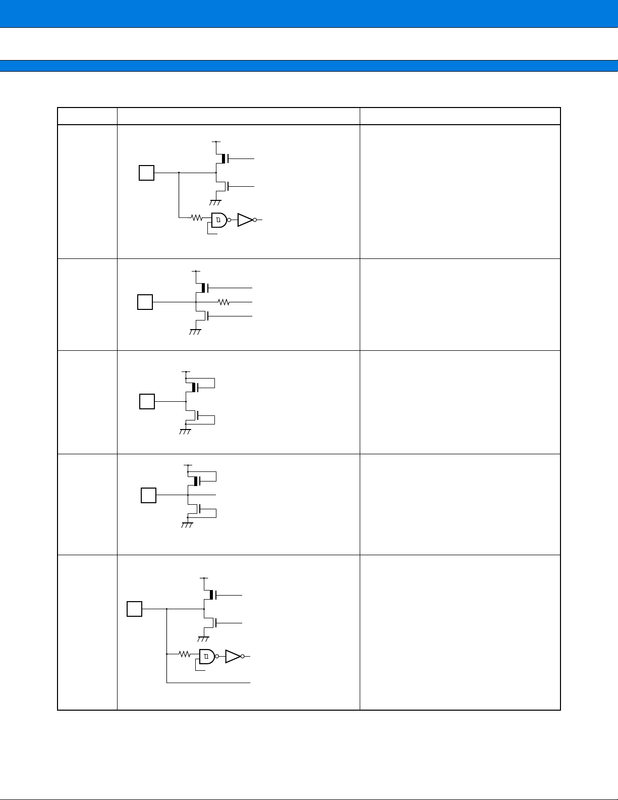
• Input/output port
PDR (port data register)
PDR read
Output latch
PDR write
DDR (port direction register)
Internal data bus
Direction latch
DDR write
DDR read
Standby control: Stop, timebase timer mode and SPL=1, or hardware standby mode
• Input pull-up resistor setup register (RDR)
PDR (port data register)
PDR read
Output latch
PDR write
DDR (port direction register)
Pch
Pin
Nch
Standby control (SPL=1)
To resource input
Pull-up resistor
About 50 kΩ
(5.0 V)
Pch
Pch
Pin
36
Direction latch
DDR write
Internal data bus
Standby control: Stop, timebase timer mode and SPL=1
DDR read
RDR latch
RDR write
RDR read
RDR (input pull-up resistor setup register)
Nch
Standby control
(SPL=1)

• Analog input enable register (ADER)
ADER (analog input enable register)
ADER read
ADER latch
ADER write
PDR (port data register)
PDR read
MB90520 Series
To analog input
RMW
(read-modify-write
type instruction)
Internal data bus
Output latch
PDR write
DDR (port direction register)
Direction latch
DDR write
DDR read
Standby control: Stop, timebase timer mode and SPL=1
Pch
Pin
Nch
Standby control
(SPL=1)
37

MB90520 Series
2. Timebase Timer
The timebase timer is a 18-bit free-run counter (timebase counter) for counting up in synchronization to the
internal count clock (divided-by-2 of oscillation) with an interval timer function for selecting an interval time from
four types : 2
The timebase timer also has a function for supplying operating clocks for the timer output for the oscillation
stabilization time or the watchdog timer, etc.
(1) Register Configuration
• Timebase timer control register (TBTC)
12
/HCLK, 214/HCLK, 216/HCLK, and 219/HCLK.
Address
Reserved
H
0000A9
R/W: Readable and writable
— : Undefined bits (read value undefined)
(2) Block Diagram
Timebase timer counter
Divided-by-2
of HCLK
× 2
1
× 22× 2
bit 15 bit 14 bit 13 bit 12 bit 11 bit 10 bit 9 bit 8
—
—
R/W — — R/W R/W
To 8/16-bit PPG timer
3
. . . . . .
TBIE
× 28× 29× 210× 211× 212× 213× 214× 215× 216× 217× 2
TBOF
OF
TBC1
TBR
R/W R/W
OF
TBC0
R/W
OF
Initial value
1XX00000
To watchdog timer
OF
To oscillation stabilization
time selector of clock control block
B
18
38
Power-on reset
Start stop-mode
CKSCR : MCS = 1→0*
Timebase timer control register
(TBTC)
Switch machine clock from oscillation clock to PLL clock
*1:
Interrupt number
*2:
OF : Overflow
HCLK : Oscillation clock frequency
1
Timebase timer
interrupt signal
2
#12*
Counter
clear circuit
Reserved
timer selector
Clear TBOF
——
Interval
Set TBOF
TBIE TBRTBOF TBC1 TBC0

MB90520 Series
3. Watchdog Timer
The watchdog timer is a 2-bit counter operating with an output of the timebase timer and resets the CPU when
the counter is not cleared for a preset period of time.
(1) Register Configuration
• Watchdog timer control register (WDTC)
Address
0000A8
R: Read only
W: Write only
X : Indeterminate
(2) Block Diagram
Watchdog timer
Start sleep-mode
Start hold status
Start stop-mode
bit 7 bit 6 bit 5 bit 4 bit 3 bit 2 bit 1 bit 0
H
Counter clear
control circuit
PONR STBR WRST ERST SRST WTE WT1 WT0
RRRRRWWW
Watchdog timer control register (WDTC)
PONR STBR WRST ERST SRST WTE WT1 WT0
2
CLR and start
Count clock
selector
CLR
counter
2-bit
Overflow
CLR
Watchdog timer
reset generation
circuit
Initial value
XXXXXXXX
To internal reset
generation circuit
B
Clear
(Timebase timer counter)
Divided-by-2
of HCLK
HCLK : Oscillation clock frequency
× 2
1
2
...
× 2
4
8
× 29× 210× 211× 212× 213× 214× 215× 216× 217× 2
× 2
18
39

MB90520 Series
4. 8/16-bit PPG Timer 0, 1
The 8/16-bit PPG timer is a 2-CH re-load timer module for outputting pulse having giv en frequencies/duty ratios.
The two modules perform the following operation by combining functions.
• 8-bit PPG timer output 2-CH independent output mode
This is a mode for operating independent 2-CH 8-bit PPG timers, in which PG00 and PG10 pins correspond
to outputs from PPG0 and PPG1 respectively.
• 16-bit PPG timer output operation mode
In this mode, PPG0 and PPG1 are combined to be operated as a 1-CH 8/16-bit PPG timer 0 and 1 operating
as a 16-bit timer. Because outputs during 16-bit PPG timer output operation mode are re versed by an underflow
from PPG1, the same output pulses are output from PG10 and PG11 pins.
• 8 + 8-bit PPG timer output operation mode
In this mode, PPG0 is operated as an 8-bit prescaler register, in which an underflow output of PPG0 is used
as a clock source for PPG1.
A prescaler output of PPG0 is output from PG00 and PG01 pins. PPG output of PPG1 is output from PG10 and
PG11 pins.
• PPG output operation
A pulse wave with any period/duty ratio is output. The module can also be used as a D/A converter with an
external add-on circuit.
40

(1) Register Configuration
• PPG0 operating mode control register (PPGC0)
Address
000044
H
bit 7 bit 6 bit 5 bit 4 bit 3 bit 2 bit 1 bit 0
PEN0 — PE00 PIE0 PUF0 — —
R/W — R/W R/W R/W — — —
• PPG1 operating mode control register (PPGC1)
Address
000045
H
bit 15 bit 14 bit 13 bit 12 bit 11 bit 10 bit 9 bit 8
PEN1 — PE10 PIE1 PUF1 MD1 MD0
R/W — R/W R/W R/W R/W R/W R/W
• PPG0 output control register (PPGOE0)
Address
000046
H
bit 7 bit 6 bit 5 bit 4 bit 3 bit 2 bit 1 bit 0
PCS2 PCS1 PCS0 PCM2 PCM1 PCM0 PE11 PE01
R/W R/W R/W R/W R/W R/W R/W R/W
• PPG1 output control register (PPGOE1)
Address
000046
H
bit 7 bit 6 bit 5 bit 4 bit 3 bit 2 bit 1 bit 0
PCS2 PCS1 PCS0 PCM2 PCM1 PCM0 PE11 PE01
R/W R/W R/W R/W R/W R/W R/W R/W
• PPG0 re-load register H (PRLH0)
Address
000041
H
bit 15 bit 14 bit 13 bit 12 bit 11 bit 10 bit 9 bit 8
R/W R/W R/W R/W R/W R/W R/W R/W
MB90520 Series
Initial value
Reserved
Reserved
0X000XX1
Initial value
0X000001
Initial value
00000000
Initial value
00000000
Initial value
XXXXXXXX
B
B
B
B
B
• PPG1 re-load register H (PRLH1)
Address
000043
H
bit 15 bit 14 bit 13 bit 12 bit 11 bit 10 bit 9 bit 8
R/W R/W R/W R/W R/W R/W R/W R/W
• PPG0 re-load register L (PRLL0)
Address
000040
H
bit 7 bit 6 bit 5 bit 4 bit 3 bit 2 bit 1 bit 0
R/W R/W R/W R/W R/W R/W R/W R/W
• PPG1 re-load register L (PRLL1)
Address
H
000042
R/W:Readable and writable
X : Indeterminate
— : Undefined bits (read value undefined)
bit 7 bit 6 bit 5 bit 4 bit 3 bit 2 bit 1 bit 0
R/W R/W R/W R/W R/W R/W R/W R/W
Initial value
XXXXXXXX
Initial value
XXXXXXXX
Initial value
XXXXXXXX
B
B
B
41

MB90520 Series
(2) Block Diagram
• Block diagram of 8/16-bit PPG timer 0
PPG0 re-load
register
PRLH0
PRLL0
PEN0
Data bus for “H” digits
Data bus for “L” digits
PPG0 operating mode
control register (PPGC0)
— PE00 PIE0 PUF0 — —
Reserved
Temporary buffer
(PRLBH0)
Re-load selector
L/H selector
Count value
Re-load
Down counter
(PCNT0)
CLK
Timebase timer output (512/HCLK)
Peripheral clock (16/φ)
Peripheral clock (8/φ)
Peripheral clock (4/φ)
Peripheral clock (2/φ)
Peripheral clock (1/φ)
Select signal
Underflow
Reverse
Clear
output latch
Select signal
PPG0
Count
clock
selector
3
Pulse selector
PPG output
control circuit
R
SQ
2
Oprating mode
control signal
PPG1 underflow
PPG0 underflow
(to PPG1)
Pin
P36/PG00
Pin
P37/PG01
Interrupt
request
#19*
42
PCS2 PCS1 PCS0 PCM2 PCM1 PCM0 PE11 PE01
PPG0, 1 output control register (PPGOE0,1)
* : Interrupt number
HCLK: Oscillation clock frequency
φ : Machine clock frequency

• Block diagram of 8/16-bit PPG timer 1
PPG1 re-load
register
PRLL0
Operating
mode
control signal
PRLH0
PEN1
MB90520 Series
Data bus for “H” digits
Data bus for “L” digits
PPG1 operating mode
control register (PPGC1)
— PEI0 PIE1 PUF1 MD1 MD0
2
Reserved
Temporary buffer
(PRLBH1)
Count value
PPG1 underflow
(to PPG0)
PPG0 underflow
Timebase timer output (512/HCLK)
Re-load selector
(L/H selector)
Re-load
Down counter
(PCNT1)
CLK
Peripheral clock (16/φ)
Peripheral clock (8/φ)
Peripheral clock (4/φ)
Peripheral clock (2/φ)
Peripheral clock (1/φ)
Underflow
Select signal
Clear
PPG1
Reverse
PPG output control circuit
output latch
MD0
R
SQ
Pin
P40/PG10
Pin
P41/PG11
Interrupt
request
#23*
* : Interrupt number
HCLK: Oscillation clock frequency
φ : Machine clock frequency
Count clock selector
Select signal
PCS23PCS1 PCS0 PCM2 PCM1 PCM0 PE11 PE01
PPG0, 1 Output control register (PPGOE0, 1)
43

MB90520 Series
5. 16-bit Re-load Timer 0, 1 (With an Event Count Function)
The 16-bit re-load timer has an internal clock mode for counting down in synchronization to three types of internal
clocks and an event count mode for counting down by detecting a given edge of the pulse input to the external
bus pin. Either of the two functions can be selectively used.
For this timer, an “underflow” is defined as the timing of transition from the counter value of “0000
H” to “FFFFH.”
According to this definition, an underflow occurs after a counter value of [re-load register setting value + 1] .
In operating the counter, the re-load mode for repeating counting operation after re-loading a counter value after
an underflow or the one-shot mode for stopping the counting operation after an underflow can be selectively used.
Because the timer can generate an interrupt upon an underflow, the timer conforms to the extended intelligent
2
I/O service (EI
OS).
The MB90520 series has 2 channels of 16-bit re-load timers.
(1) Register Configuration
• Timer control status register upper digits ch.0, ch.1 (TMCSR0, TMCSR1 : H)
TMCSR0 : 000049
Address
TMCSR1 : 00004D
bit 15 bit 14 bit 13 bit 12 bit 11 bit 10 bit 9 bit 8
H
— — — — CSL1 CSL0 MOD2 MOD1
H
————R/WR/WR/WR/W
Initial value
XXXX0000
B
• Timer control status register lower digits ch.0, ch.1 (TMCSR0, TMCSR1 : L)
TMCSR0 : 000048
Address
TMCSR1 : 00004C
bit 7 bit 6 bit 5 bit 4 bit 3 bit 2 bit 1 bit 0
H
MOD0 OUTE OUTL RELD INTE UF CNTE TRG
H
R/W R/W R/W R/W R/W R/W R/W R/W
Initial value
00000000
B
• 16-bit timer register upper and lower digits ch.0, ch.1 (TMR0, TMR1)
Address
TMR0 : 00004B
00004A
TMR1 : 00004E
00004F
bit 15 bit 14 bit 13 bit 12 bit 11 bit 10 bit 9 bit 8 bit 7 bit 6 bit 5 bit 4 bit 3 bit 2 bit 1 bit 0
H
H
H
RRRRRRRRRRRRRRRR
H
Initial value
XXXXXXXX
XXXXXXXX
XXXXXXXX
XXXXXXXX
B
B
B
B
• 16-bit re-load register upper and lower digits ch.0, ch.1 (TMRLR0, TMRLR1)
TMRLR0 : 00004B
Address
00004A
TMRLR1 : 00004E
00004F
R/W: Readable and writable
R : Read only
W : Write only
X : Indeterminate
— : Undefined bits (read value undefined)
bit 15 bit 14 bit 13 bit 12 bit 11 bit 10 bit 9 bit 8 bit 7 bit 6 bit 5 bit 4 bit 3 bit 2 bit 1 bit 0
H
H
H
WWWWWWWWWWWWWWWW
H
44
Initial value
XXXXXXXX
XXXXXXXX
XXXXXXXX
XXXXXXXX
B
B
B
B

(2) Block Diagram
MB90520 Series
Internal data bus
TMRLR0*
1
<TMRLR1>
1
TMR0*
<TMR1>
16-bit timer register (down counter) UF
Count clock generation circuit
3
Pin
φ
Prescaler
Input
control
circuit
External
clock
P70/TI0/OUT4*
<P72/TI1/OUT6>
1
32
Function select
16-bit re-load register
CLK
Gate input
Valid clock
decision
circuit
Internal
clock
Clock
selecter
Re-load signal
CLKClear
Select
signal
Wait signal
Output control circuit
Output signal
generation
circuit
Reverse
Re-load
control
circuit
EN
Operation
control
circuit
To UART *
<To 8/10-bit
1
A/D converter>
Pin
P71/TO0/OUT5*
<P73/TO1/OUT7>
1
————
Timer control status register (TMCSR0)*
CSL1 CSL0 MOD2MOD1MOD0OUTE OUTL RELD INTE UF CNTE TRG
1
<TMCSR1>
*1: The timer has ch.0 and ch.1, and figures bracketed by < > are for ch.1
*2: Interrupt number
φ: Machine clock frequency
Clear
2
CS
EI
Interrupt request signal
1, *2
#38*
<#40>
45

MB90520 Series
6. 16-bit I/O Timer
The 16-bit I/O timer module consists of two 16-bit free-run timers, two input capture circuits (ICU), and eight
output comparators (OCU). This module allows two independent waveforms to be output on the basis of the
16-bit free-run timer. Input pulse width and external clock periods can, therefore, be measured.
•Block diagram
Internal data bus
Input capture 0, 1
(ICU)
Dedicated
bus
16-bit
free-run timer 1, 2
Dedicated
bus
Output compare 0, 1
(OCU)
46

MB90520 Series
(1) 16-bit Free-run Timer 1, 2
The 16-bit free-run timer consists of a 16-bit up counter, a control register and a communications prescaler
register. The value output from the timer counter is used as basic time (base timer) for input capture (ICU) and
output compare (OCU).
• A counter operation clock can be selected from four internal clocks (φ/4, φ/16, φ/64 and φ/256).
• An interrupt can be generated by overflow of counter value or compare match with OCU compare register 0
and 4. (Compare match requires mode settings.)
• The counter value can be initialized to “0000
register 0 and 4.
• Register configuration
• Free-run timer data register 1, 2 (TCDT1, TCDT2)
H” by a reset, software clear or compare match with OCU compare
TCDT1 : 000057
Address
000056
TCDT2 : 000067
000066
bit 15bit 14bit 13bit 12bit 11bit 10 bit 9 bit 8 bit 7 bit 6 bit 5 bit 4 bit 3 bit 2 bit 1 bit 0
H
T15 T14 T13 T12 T11 T10 T9 T8 T7 T6 T5 T4 T3 T2 T1 T0
H
H
R/W R/W R/W R/W R/W R/W R/W R/W R/W R/W R/W R/W R/W R/W R/W R/W
H
• Free-run timer control status register 1, 2 (TCCS1, TCCS2)
Address
TCCS1 : 000058
TCCS2 : 000068
R/W: Readable and writable
bit 7 bit 6 bit 5 bit 4
H
Reserved
H
IVF
STOPIVFE CLRMODE CLK0CLK1
bit 3 bit 2 bit 1 bit 0
R/W R/W R/W R/W R/W R/W R/W R/W
• Block diagram
Free-run timer data register (TCDT1)*1 <TCDT2>
Communications
φ
prescaler register
2
Free-run timer
control status register
(TCCS1) *
1
<TCCS2>
Reserved
OF
IVF IVFE STOP MODE CLR CLK1 CLK0
16-bit counter
STOPCLK CLR
Count value output
to ICO and OCU
OCU compare register 0
match signal
Initial value
00000000
00000000
00000000
00000000
Initial value
00000000
00000000
Internal data bus
B
B
B
B
B
B
*1: The timer has ch.1 and ch.2, and figures bracketed by < > are for ch.2.
*2: Interrupt number
φ:Machine clock frequency
OF: Overflow
16-bit free-run timer
interrupt request
1, *2
#14*
<#28>
47

MB90520 Series
(2) Input Capture 0, 1 (ICU)
The input capture (ICU) generates an interrupt request to the CPU while storing the current counter value of
the 16-bit free-run timer to the ICU data register (IPCP) upon input of a trigger edge from the external pin.
There are two sets (two channels) of input capture external pins and ICU data registers, enabling measurements
of a maximum of four events.
• The input capture has two sets of external input pins (IN0, IN1) and ICU registers (IPCP), enabling
measurements of a maximum of four events.
• Trigger edge direction can be selected from rising/falling/both edges.
• The input capture can be set to generate an interrupt request at the storage timing of the counter value of the
16-bit free-run timer to the ICU data register (IPCP).
• The input compare conforms to the extended intelligent I/O service (EI
• The input capture ( ICU) function is suited for measurements of intervals (frequencies) and pulse-widths.
• Register configuration
2
OS).
• ICU data register ch.0 ch.1 (IPCP0, IPCP1)
IPCP0(upper) : 000051
IPCP1(upper) : 000053
IPCP0(lower) : 000050
IPCP1(lower) : 000052
Address Initial value
Address Initial value
Note: This register holds a 16-bit free-run timer value when the valid edge of the corresponding external pin input waveform
is detected. (This register can be word-accessed, but not programmed.)
bit 15 bit 14
H
CP15 CP14
H
R
bit 7
H
CP07
H
R
R
bit 6
CP06
R
bit 13 bit 12 bit 11 bit 10 bit 9
CP13
R
bit 5
CP05
RR
CP12 CP11
RR
bit 4 bit 3
CP04 CP03
R
CP10 CP09
R
bit 2 bit 1 bit 0
CP02
R
R
CP01
RR
bit 8
CP08
R
CP00
• ICU control status register (ICS01)
Address
000054
R/W: Readable and writable
R : Read only
X :Indeterminate
bit 7
H
ICP1
R/W
bit 6 bit 5
ICP0
R/W
ICE1 ICE0
R/W
bit 4
R/W
bit 3
EG11 EG10 EG01
R/W R/W
bit 2 bit 1
R/W
bit 0
EG00
R/W
XXXXXXXX
XXXXXXXX
Initial value
00000000
B
B
B
48

•Block diagram
P20/IC00
Pin
P21/IC01
Pin
P22/IC10
Pin
P23/IC11
Pin
ICU control status register (ICS01)
Edge detection circuit
Data latch signal
2
2
ICP1
ICP0 ICE1 ICE0 EG11 EG10 EG01 EG00
Internal data bus
Output latch
IPCP0(upper)
IPCP1(upper)
Latch
signal
MB90520 Series
ICU data register (IPCP)
IPCP0(lower)
IPCP1(lower)
16
16
16-bit free-run
timer 1, 2
* : Interrupt number
Interrupt request
#31*
Interrupt request
#32*
49

MB90520 Series
(3) Output Compare 0, 1 (OCU)
The output compare (OCU) is two sets of compare units each consisting of an eight-channel OCU compare
register, a comparator and a control register.
An interrupt request can be generated for each channel upon a match detection by performing time-division
comparison between the OCU compare data register setting value and the counter value of the 16-bit free-run
timer.
The OUT pin can be used as a waveform output pin for reversing output upon a match detection or a generalpurpose output port for directly outputting the setting value of the CMOD bit.
C
•Register
• OCU control status register ch.01, ch.23, ch.45, ch.67 (OCS01, OCS23, OCS45, OCS67)
ch.01 : OCS01 (upper) : 0000063
ch.23 : OCS23 (upper) : 0000065
ch.45 : OCS45 (upper) : 000002D
ch.67 : OCS67 (upper) : 000002F
ch.01 : OCS01 (lower) : 000062
ch.23 : OCS23 (lower) : 000064
ch.45 : OCS45 (lower) : 00002C
ch.67 : OCS67 (lower) : 00002E
onfiguration
Address
Address
bit 15 bit 14 bit 13 bit 12 bit 11 bit 10 bit 9 bit 8
H
H
H
H
— — — CMOD OTE1 OTE0 OTD1 OTD0
— — — R/W R/W R/W R/W R/W
Initial value
XXX00000
bit 7 bit 6 bit 5 bit 4 bit 3 bit 2 bit 1 bit 0
H
H
H
H
ICP1 ICP0 ICE1 ICE0 — — CST1 CST0
R/W R/W R/W R/W — — R/W R/W
Initial value
0000XX00
B
B
• OCU control status register ch.0 to ch.7 (OCS0 to OCS7)
ch.0 : OCP0 (upper) : 00005B
Address
ch.1 : OCP1 (upper) : 00005D
ch.2 : OCP2 (upper) : 00005F
ch.3 : OCP3 (upper) : 000061
ch.4 : OCP4 (upper) : 00000D
ch.5 : OCP5 (upper) : 00001D
ch.6 : OCP6 (upper) : 000035
ch.7 : OCP7 (upper) : 00006D
Address
ch.0 : OCP0 (lower) : 00005A
ch.1 : OCP1 (lower) : 00005C
ch.2 : OCP2 (lower) : 00005E
ch.3 : OCP3 (lower) : 000060
ch.4 : OCP4 (lower) : 00000C
ch.5 : OCP5 (lower) : 00001C
ch.6 : OCP6 (lower) : 000034
ch.7 : OCP7 (lower) : 00006C
R/W: Readable and writable
X : Indeterminate
— : Undefined bits (read value undefined)
H
H
H
H
H
H
H
H
H
H
H
H
H
H
H
H
bit 15 bit 14 bit 13 bit 12 bit 11 bit 10 bit 9 bit 8
C15C14C13C12C11C10C09C08
R/W R/W R/W R/W R/W R/W R/W R/W
bit 7 bit 6 bit 5 bit 4 bit 3 bit 2 bit 1 bit 0
C07 C06 C05 C04 C03 C02 C01 C00
R/W R/W R/W R/W R/W R/W R/W R/W
Initial value
XXXXXXXX
Initial value
XXXXXXXX
B
B
50

• Block diagram
• Output compare 0 (OCU)
MB90520 Series
OCU control status register ch. 23 (OCS23)
—
OCP3
OCP2
Internal data bus
OCP1
CMOD
——
16-bit free-run timer 1
Compare control circuit 3
OCU compare register ch. 3
Compare control circuit 2
OCU compare register ch. 2
Compare control circuit 1
OCU compare register ch.1
Compare control circuit 0
OTE1 OTE0 OTD1 OTD0 ICP1 ICP0 ICE1 ICE0
#36*
#35*
Output
control
circuit 3
Output
control
circuit 2
Output
control
circuit 1
Output
control
circuit 0
CST1 CST0
——
2
2
Output compare
interrupt request
P35/OUT3
Pin
P34/OUT2
Pin
P33/OUT1
Pin
P32/OUT0
Pin
OCP0
OCU compare register ch. 0
———
OCU control status register ch. 01
(OCS01)
* : Interrupt number
2
CMOD
OTE1 OTE0 OTD1 OTD0 ICP1 ICP0 ICE1 ICE0
2
——
#34*
#33*
CST1 CST0
Output compare
interrupt request
51

MB90520 Series
• Output compare 1(OCU)
OCU control status register ch. 67 (OCS67)
—
OCP7
OCP6
Internal data bus
OCP5
——
CMOD
OTE1 OTE0 OTD1 OTD0 ICP1 ICP0 ICE1 ICE0 CST1 CST0
16-bit free-run timer 2
Compare control circuit 7
OCU compare register ch. 7
Compare control circuit 6
OCU compare register ch. 6
Compare control circuit 5
OCU compare register ch. 5
Compare control circuit 4
#27*
Output compare
interrupt request
——
2
2
P73/TO1/OUT7
Output control
circuit 7
Pin
P72/TI1/OUT6
Output control
circuit 6
Pin
P71/TO0/OUT5
Output control
circuit 5
Pin
P70/TI0/OUT4
Output control
circuit 4
Pin
52
OCP4
* : Interrupt number
OCU compare register ch. 4
———
CMOD
OTE1 OTE0 OTD1 OTD0 ICP1 ICP0 ICE1 ICE0 CST1 CST0
OCU control status register ch. 45 (OCS45)
2
2
——
Output compare
#25*
interrupt request

MB90520 Series
7. 8/16-bit Up/Down Counter/Timer 0, 1
The 8/16-bit up/down counter/timer consists of six event input pins, two 8-bit up/down counters, two 8-bit
re-load compare registers, and their controllers.
(1) Register Configuration
• Up/down count register 0 (UDCR0)
Address
000080
H
bit 7 bit 6 bit 5 bit 4
D06D07
RRRRRRRR
• Up/down count register 1 (UDCR1)
Address
000081
bit 15 bit 14 bit 13 bit 12 bit 11 bit 10 bit 9 bit 8
H
D17 D16 D15 D14 D13 D12 D11 D10
RRRRRRRR
• Re-load compare register 0 (RCR0)
Address
H
000082
• Re-load compare register 1 (RCR1)
Address
H
000083
bit 7 bit 6 bit 5 bit 4
D06D07
WWWWWWWW
bit 15 bit 14 bit 13 bit 12 bit 11 bit 10 bit 9 bit 8
D17 D16 D15 D14 D13 D12 D11 D10
WWWWWWWW
• Counter status register 0, 1 (CSR0, CSR1)
Address
CSR0 : 000084
CSR1 : 000088
H
H
bit 7 bit 6 bit 5 bit 4
CITECSTR
R/W R/W R/W R/W R/W R/W R R
• Counter control register 0, 1 (CCRL0, CCRL1)
Address
CCRL0 : 000086
CCRL1 : 00008A
H
H
bit 7 bit 6 bit 5 bit 4
CTUT
—
R/W R/W R/W R/W R/W R/W R/W
—
• Counter control register 0 (CCRH0)
Address
000087
H
bit 15 bit 14 bit 13 bit 12 bit 11 bit 10 bit 9 bit 8 Initial value
M16E CDCF CFIE CLKS CMS1 CMS0 CES1 CES0
R/W R/W R/W R/W R/W R/W R/W R/W
• Counter control register 1 (CCRH1)
Address
00008B
bit 15 bit 14 bit 13 bit 12 bit 11 bit 10 bit 9 bit 8
H
CDCF CFIE CLKS CMS1 CMS0 CES1 CES0
—
R/W R/W R/W R/W R/W R/W R/W
—
bit 3 bit 2 bit 1 bit 0
D04D05 D02D03 D00D01
bit 3 bit 2 bit 1 bit 0
D04D05 D02D03 D00D01
bit 3 bit 2 bit 1 bit 0
CMPFUDIE UDFFOVFF UDF0UDF1
bit 3 bit 2 bit 1 bit 0
RLDEUCRE CGSCUDCC CGE0CGE1
Initial value
00000000
Initial value
00000000
Initial value
00000000
Initial value
00000000
Initial value
00000000
Initial value
X0000000
00000000
Initial value
X0000000
B
B
B
B
B
B
B
B
R/W: Readable and writable
R : Read only
W : Write only
— : Undefined bits (read value undefined)
53

MB90520 Series
(2) Block Diagram
• Block diagram of 8/16-bit up/down counter/timer 0
Internal data bus
RCR0
Re-load compare register 0
UDCR0
Up/down count register 0
Counter control
register 0 (CCRL0)
UDCC
—
CTUT CGE1 CGE0UCRE
RLDE
CGSC
Re-load
control
circuit
CARRY/
BORROW
(to channel 1)
P26/ZIN0/INT7
Pin
φ
P24/AIN0
Pin
Pin
P25/BIN0
CDCF CES1 CES0CFIE CMS1CLKS CMS0
M16E
Counter control register 0 (CCRH0)
* : Interrupt number
φ: Machine clock frequency
Edge/level
detection
circuit
Prescaler
UP/down count
clock selector
Counter clear
circuit
Count clock
Counter status
register 0 (CSR0)
CSTR CITE UDIE CMPF OVFF UDFF UDF1 UDF0
Overflow
Underflow
Compare
control circuit
Interrupt request
#21*
Interrupt request
#22*
M16E
(to channel 1)
54

MB90520 Series
• Block diagram of 8/16-bit up/down counter/timer 1
Internal data bus
RCR1
Re-load compare register 1
UDCR1
Up/down count register 1
Counter control
register 1 (CCRL1)
CGSC
Counter clear
UP/down count
clock selector
circuit
Count clock
Counter status
register 1
CSTR CITE UDIE CMPF OVFF UDFF UDF1 UDF0
P52/SCK2/ZIN1
Pin
CARRY/BORRW
(from channel 0)
P50/SIN2/AIN1
Pin
CTUT CGE1 CGE0UCRE UDCCRLDE
—
Edge/level
detection
circuit
φ
Prescaler
(CSR1)
Overflow
Underflow
Re-load
control
circuit
Compare
control circuit
Pin
P51/SOT2/BIN1
M16E
(from channel 1)
—
Counter control register 1 (CCRH1)
* : Interrupt number
φ: Machine clock frequency
Interrupt request
#29*
Interrupt request
#30*
CDCF CES1 CES0CFIE CMS1CLKS CMS0
55

MB90520 Series
8. Extended I/O Serial Interface 0, 1
The extended I/O serial interface transfers data using a clock synchronization system having an 8-bit x 1 channel
configuration.
For data transfer, you can select LSB first/MSB first.
(1) Register Configuration
• Serial mode control upper status register 0, 1 (SMCSH0, SMCSH1)
SMCSH0 : 000025
SMCSH1 : 000029
Address
• Serial mode control lower status register 0, 1 (SMCSL0, SMCSL1)
Address
SMCSL0 : 000024
SMCSL1 : 000028
• Serial data register 0, 1 (SDR0, SDR1)
SDR0 : 000026
SDR1 : 00002A
H
H
Address
bit 15 bit 14 bit 13 bit 12 bit 11 bit 10 bit 9 bit 8
H
SMD2 SMD1 SMD0 SIE SIR BUSY STOP STRT
H
R/W R/W R/W R/W R/W R R/W R/W
bit 7 bit 6 bit 5 bit 4
——
————
H
H
bit 7 bit 6 bit 5 bit 4
D6D7
R/W R/W R/W R/W R/W R/W R/W R/W
bit 3 bit 2 bit 1 bit 0
——
R/W R/W R/W R/W
D4D5 D2D3 D0D1
BDSMODE SCOESOE
bit 3 bit 2 bit 1 bit 0
Initial value
00000010
Initial value
XXXX0000
Initial value
XXXXXXXX
B
B
B
R/W: Readable and writable
R : Read only
X :Indeterminate
— : Undefined bits (read value undefined)
56

(2) Block Diagram
(MSB first) D0 to D7 D7 to D0 (LSB first)
MB90520 Series
Internal data bus
Pin
P45/SIN1
Pin
P50/SIN2/AIN1
Pin
P47/SCK1
Pin
P52/SCK2/ZIN1
Internal clock
210
SMD2 SMD1 SMD0 SIE SIR BUSY STOP STRT
Serial mode control
status register
(SMCSH
*: Interrupt number
,L)
Serial data register
(SDR)
Control circuit
3
Transfer direction selection
Read
Write
Shift clock counter
————
MODE
Pin
P46/SOT1
Pin
P51/SOT2/BIN1
BDS SOE
Interrupt request
#15 (SMCS0)*
#17 (SMCS1)*
SCOE
57

MB90520 Series
9. UART (SCI)
UART (SCI) is a general-purpose serial data communication interface for performing synchronous or
asynchronous communication (start-stop synchronization system).
• Data buffer: Full-duplex double buffer
• Transfer mode:Clock synchronized (with start and stop bit)
Clock asynchronized (start-stop synchronization system)
• Baud rate:Embedded dedicated baud rate generator
External clock input possible
Internal clock (a clock supplied from 16-bit re-load timer 0 can be used.)
Asynchronization 9615 bps/31250 bps/4808 bps/2404 bps/1202 bps
CLK synchronization 1 Mbps/500 kbps/250 kbps/125 kbps/62.5 kbps
• Data length:8 bit (without a parity bit)
7 bit (with a parity bit)
• Signal format: NRZ (Non Return to Zero) system
• Reception error detection: Framing error
Overrun error
Parity error (multi-processor mode is supported, enabling setup of any baud rate
by an external clock.)
• Interrupt request: Receive interrupt (reception complete, receive error detection)
Transmit interrupt (transmisson complete)
Transmit/receive conforms to extended intelligent I/O service (EI
Internal machine clock
For 6 MHz, 8 MHz, 10 MHz,
}
12 MHz and 16 MHz
2
OS)
58

(1) Register Configuration
MB90520 Series
• Serial control register (SCR)
Address
H
000021
bit 15 bit 14 bit 13 bit 12 bit 11 bit 10 bit 9 bit 8
PEN P SBL CL A/D REC RXE TXE
R/W R/W R/W R/W R/W W R/W R/W
• Serial mode register (SMR)
Address
H
000020
bit 7 bit 6 bit 5 bit 4 bit 3 bit 2 bit 1 bit 0
MD1 MD0 CS2 CS1 CS0
R/W R/W R/W R/W R/W R/W R/W R/W
• Serial status register (SSR)
Address
000023
H
bit 15 bit 14 bit 13 bit 12 bit 11 bit 10 bit 9 bit 8
PE ORE FRE RDRF TRDE — RIE TIE
RR RRR—R/WR/W
• Serial input data register (SIDR)
Address
000022
H
bit 7 bit 6 bit 5 bit 4 bit 3 bit 2 bit 1 bit 0
D7 D6 D5 D4 D3 D2 D1 D0
RRRRRRRR
• Serial output data register (SODR)
Address
000022
H
bit 7 bit 6 bit 5 bit 4 bit 3 bit 2 bit 1 bit 0
D7 D6 D5 D4 D3 D2 D1 D0
WWWWWWWW
• Communications prescaler control register (CDCR)
Address
000027
H
bit 15 bit 14 bit 13 bit 12 bit 11 bit 10 bit 9 bit 8
MD — — — DIV3 DIV2 DIV1 DIV0
R/W — — — R/W R/W R/W R/W
Reserved
SCKE SOE
Initial value
00000100
Initial value
00000000
Initial value
00001X00
Initial value
XXXXXXXX
Initial value
XXXXXXXX
Initial value
0XXX1111
B
B
B
B
B
B
R/W:Readable and writable
R : Read only
W:Write only
X : Indeterminate
— : Undefined bits (read value undefined)
59

MB90520 Series
(2) Block Diagram
Dedicated baud
rate generator
16-bit re-load timer 0
External clock
Pin
P42/SCK0
Clock
selector
Receive
clock
detection circuit
Receive
control circuit
Start bit
Control bus
Transmit
clock
Transmit
control circuit
Transmit start
circuit
Receive
interrupt signal
#37*
Transmit
interrupt signal
#39*
Pin
P42/SIN0
Receive condition
decision circuit
SMR
register
Receive bit
Receive parity
Shift register for
reception
MD1
MD0
CS2
CS1
CS0
SCKE
SOE
counter
counter
SIDR SODR
Reception
complete
Internal data bus
SCR
register
Transmit bit
counter
Transmit parity
counter
Shift register for
transmission
PEN
P
SBL
CL
A/D
REC
RXE
TXE
SSR
register
Pin
P43/SOT0
Start transmission
2
OS reception
To EI
error generation
signal (to CPU)
PE
ORE
FRE
RDRF
TDRE
RIE
TIE
60
* : Interrupt number

MB90520 Series
10. DTP/External Interrupt Circuit
The DTP (Data Transfer Peripheral), which is located between the peripheral circuit outside the device and the
2
F
MC-16LX CPU, receives an interrupt request or DMA request generated by the external peripheral circuit*
for transmission to the F
As with request levels, two types of “H” and “L” can be selected for the intelligent I/O service. Rising and falling
edges as well as “H” and “L” can be selected for an external interrupt request.
* :The external peripheral circuit is connected outside the MB90520 series device.
(1) Register Configuration
• DTP/interrupt factor register (EIRR)
Address
000031
• DTP/interrupt enable register (ENIR)
Address
000030
• Request level setting register (ELVR)
Address
ELVR (lower) : 000032
2
MC-16LX CPU. It is used to activate the intelligent I/O service or interrupt processing.
bit 15 bit 14 bit 13 bit 12 bit 11 bit 10 bit 9 bit 8
ER7 ER6 ER5 ER4 ER3 ER2 ER1 ER0
H
R/W R/W R/W R/W R/W R/W R/W R/W
bit 7 bit 6 bit 5 bit 4 bit 3 bit 2 bit 1 bit 0
H
EN7 EN6 EN5 EN4 EN3 EN2 EN1 EN0
R/W R/W R/W R/W R/W R/W R/W R/W
bit 7 bit 6 bit 5 bit 4 bit 3 bit 2 bit 1 bit 0
H
LB3 LA3 LB2 LA2 LB1 LA1 LB0 LA0
R/W R/W R/W R/W R/W R/W R/W R/W
Initial value
XXXXXXXX
Initial value
00000000
Initial value
00000000
B
B
B
Address
ELVR (upper) : 000033
R/W: Readable and writable
X : Indeterminate
bit 15 bit 14 bit 13 bit 12 bit 11 bit 10 bit 9 bit 8
LB7 LA7 LB6 LA6 LB5 LA5 LB4 LA4
H
R/W R/W R/W R/W R/W R/W R/W R/W
Initial value
00000000
B
61

MB90520 Series
(2) Block Diagram
selector 1
Level edge
22
selector 3
22
Level edge
selector 5
Level edge
selector 0
Level edge
selector 2
Level edge
selector 4
Level edge
DTP/external interrupt
input detection circuit
Interrupt request signal
#24*
DTP/interrupt factor register (EIRR)
#20*
#18*
#13*
DTP/interrupt enable register (ENIR)
62
Request level setting register (ELVR)
222
LB7 LA7 LB6 LA6 LB5 LA5 LB4 LA4 LB3 LA3 LB2 LA2 LB1 LA1 LB0 LA0
2
Pin
selector 7
Level edge
P26/ZIN0/INT7
Pin
P06/INT6
selector 6
Level edge
Pin
P05/INT5
P04/INT4
Internal data bus
ER7 ER0ER6ER5ER4ER3ER2ER1
Pin
Pin
P03/INT3
Pin
P02/INT2
Pin
P01/INT1
EN7 EN0EN6EN5EN4EN3EN2EN1
P00/INT0
*: Interrupt number

MB90520 Series
11.Wake-up Interrupt
Wake-up interrupts transmit interrupt request (“L” level) generated by peripheral equipment located between
external peripheral devices and the F
The interrupt does not conform to the exterded intelligent I/O service (EI
(1) Register Configuration
• Wake-up interrupt flag register (EIFR)
2
MC-16LX CPU to the CPU and invoke interrupt processing.
2
OS).
Address
00000F
bit 15 bit 14 bit 13 bit 12 bit 11 bit 10 bit 9 bit 8
H
———————WIF
———————R/W
• Wake-up interrupt enable register (EICR)
Address
00001F
R/W: Readable and writable
W : Write only
— : Undefined bits (read value undefined)
bit 15 bit 14 bit 13 bit 12 bit 11 bit 10 bit 9 bit 8
H
EN7 EN6 EN5 EN4 EN3 EN2 EN1 EN0
WWWWWWWW
(2) Block Diagram
Wake-up interrupt
enable register (EICR)
EN7 EN6 EN5 EN4 EN3 EN2 EN1 EN0 — — —
P10/WI0 Pin
Internal data bus
XXXXXXX0
Wake-up interrupt flag
register (EIFR)
————WIF
Interrupt request detection circuit
Initial value
Initial value
00000000
B
B
P11/WI1
P12/WI2
P13/WI3
P14/WI4
P15/WI5
P16/WI6
P17/WI7
Pin
Pin
Pin
Pin
Pin
Pin
Pin
*: Interrupt number
Wake-up interrupt
request
#16*
63

MB90520 Series
12. Delayed Interrupt Generation Module
The delayed interrupt generation module generates interrupts for switching tasks. By using this module,
hardware interrupt requests to the CPU can be generated and cancelled using software.
2
This module does not conform to the extended intelligent I/O service (EI
(1) Register Configuration
• Delayed interrupt factor generation/cancellation register (DIRR)
Address
00009F
Note: Upon a reset, an interrupt is cancelled.
R/W: Readable and writable
— : Undefined bits (read value undefined)
bit 15 bit 14 bit 13 bit 12 bit 11 bit 10 bit 9 bit 8
H
———————R0
———————R/W
The DIRR is the register used to control delay interrupt request generation/cancellation. Programming this
register with “1” generates a delay interrupt request. Programming this register with “0” cancels a delay interrupt
request. Upon a reset, an interrupt is canceled. The undefined bit area can be programmed with either “0” or
“1.” For future extension, however, it is recommended that bit set and clear instructions be used to access this
register.
OS).
Initial value
XXXXXXX0
B
(2) Block Diagram
—
——————R0
Delayed interrupt factor generation/
cancellation register (DIRR)
*: Interrupt number
Internal data bus
S factor
R latch
Interrupt request signal
#42*
64

MB90520 Series
13. 8/10-bit A/D Converter
The 8/10-bit A/D converter converts analog voltage input to the analog input pins (input voltage) to digital values
(A/D conversion) and has the following features:
• Minimum conversion time: minim um 15.0 µs (at machine clock frequency of 16 MHz, including sampling time)
• Minimum sampling period: 4 µs/8 µs (at machine clock frequency of 16 MHz)
• Compare time: 99/176 machine cycles per channel
(99 machine cycles are used for a machine clock frequency below 10 MHz.)
• Conversion method: RC successive approximation method with a sample and hold circuit
• 8/10-bit resolution
• Analog input pins: Selectable from eight channels by software
Single conversion mode: Selects and converts one channel.
Scan conversion mode: Conv erts two or more successiv e channels. Up to eight channels can be programmed.
Continuous conversion mode: Repeatedly converts specified channels.
Stop conversion mode: Stops conversion after completing a conversion for one channel and wait for the
next activation (conversion can be started synchronously).
• Interrupt requests can be generated and the extended intelligent I/O service (EI
end of A/D conversion. Furthermore, A/D conversion result data can be transferred to the memory, enabling
efficient continuous processing.
• When interrupts are enabled, there is no loss of data ev en in contin uous operations because the conversion
data protection function is in effect.
• Starting factors for conversion: Selectable from software activation, external trigger (falling edge) and timer
(rising edge).
2
OS) can be started after the
65

MB90520 Series
(1) Register Configuration
• A/D control status register upper digits (ADCS2)
Address
H
000037
• A/D control status register lower digits (ADCS1)
Address
H
000036
• A/D data register upper digits (ADCR2)
Address
H
000039
• A/D data register lower digits (ADCR1)
Address
H
000038
bit 15 bit 14 bit 13 bit 12 bit 11 bit 10 bit 9 bit 8
BUSY INT INTE PAUS STS1 STS0 STRT
R/W R/W R/W R/W R/W R/W W R/W
bit 7 bit 6 bit 5 bit 4 bit 3 bit 2 bit 1 bit 0
MD1 MD0 ANS2 ANS1 ANS0 ANE2 ANE1 ANE0
R/W R/W R/W R/W R/W R/W R/W R/W
bit 15 bit 14 bit 13 bit 12 bit 11 bit 10 bit 9 bit 8
SELB ST1 ST0 CT1 CT0 — (D9) (D8)
WWWWW—R R
bit 7 bit 6 bit 5 bit 4 bit 3 bit 2 bit 1 bit 0
D7 D6 D5 D4 D3 D2 D1 D0
RRRRRRRR
Reserved
Initial value
00000000
Initial value
00000000
Initial value
00001XXX
Initial value
XXXXXXXX
B
B
B
B
R/W: Readable and writable
R : Read only
W : Write only
X : Indeterminate
— : Undefined bits (read value undefined)
66

(2) Block Diagram
MB90520 Series
A/D control status
register (ADCS)
BUSY INT INTE
P27/ADTG
P73/TO1/OUT7
P67/AN7
P66/AN6
P65/AN5
P64/AN4
P63/AN3
P62/AN2
P61/AN1
P60/AN0
Interrupt request #11*
Reserved
STS1 STS0
PAUS
Clock selector Decoder
Analog
channel
selector
STRT
φ
Sample hold
circuit
AVRH, AVRL
MD1 MD0 ANS2 ANS1 ANS0 ANE2 ANE1 ANE0
6
2
Comparator
Control circuit
CC
AV
AV
8-bit D/A converter
SS
Internal data bus
A/D data register
(ADCR)
SELB
ST1ST0CT1CT0—(D9)(D8)D7D6D5D4D3D2D1D0
TO : 16-bit re-load timer channel 1 output
* : Interrupt number
φ : Machine clock frequency
67

MB90520 Series
14. 8-bit D/A Converter
The 8-bit D/A converter, which is based on the R-2R system, supports 8-bit resolution mode. It contains two
channels, each of which can be controlled in terms of output by the D/A control register.
(1) Register Configuration
• D/A converter data register ch.0 (DADR0)
Address
H
00003A
• D/A converter data register ch.1 (DADR1)
Address
H
00003B
• D/A control register 0 (DACR0)
Address
H
00003C
bit 7 bit 6 bit 5 bit 4 bit 3 bit 2 bit 1 bit 0
DA07 DA06 DA05 DA04 DA03 DA02 DA01 DA00
R/W R/W R/W R/W R/W R/W R/W R/W
bit 15 bit 14 bit 13 bit 12 bit 11 bit 10 bit 9 bit 8
DA17 DA16 DA15 DA14 DA13 DA12 DA11 DA10
R/W R/W R/W R/W R/W R/W R/W R/W
bit 7 bit 6 bit 5 bit 4 bit 3 bit 2 bit 1 bit 0
———————DAE0
———————R/W
Initial value
XXXXXXXX
Initial value
XXXXXXXX
Initial value
XXXXXXX0
B
B
B
• D/A control register 1 (DACR1)
Address
H
00003D
R/W: Readable and writable
X : Indeterminate
— : Undefined bits (read value undefined)
bit 15 bit 14 bit 13 bit 12 bit 11 bit 10 bit 9 bit 8
———————DAE1
———————R/W
Initial value
XXXXXXX0
B
68

•Block Diagram
Internal data bus
D/A converter data register ch.1 (DADR1) D/A converter data register ch.0 (DADR0)
DA17
DA16 DA15 DA14 DA13 DA12 DA11 DA10 DA07 DA06 DA05 DA04 DA03 DA02 DA01 DA00
D/A converter 1 D/A converter 0
DVRH DVRL
DA17
DA16
2R
Pin
R
P54/DA1
DA07
DA06
MB90520 Series
2R
R
Pin
P53/DA0
2R
2R
2R
2R
2R
2R
2R
DV
R
R
R
R
R
R
2R
SS
DA15
DA14
DA13
DA12
DA11
DA10
Standby control
D/A control register 1 (DACR1)
———————
DAE1
2R
2R
2R
2R
2R
2R
2R
DV
R
R
R
R
R
R
2R
SS
DA05
DA04
DA03
DA02
DA01
DA00
Standby control
D/A control register 0 (DACR0)
———————
DAE0
Internal data bus
69

MB90520 Series
15. Clock Timer
The clock timer control register (WTC) controls operation of the clock timer, and time for an interval interrupt.
(1) Register Configuration
• Clock timer control register (WTC)
0000AA
R/W: Readable and writable
R : Read only
X : Indeterminate
(2) Block Diagram
Timer counter
LCLK
Shift to a hardware stand-by
1
× 2
Shift to stop mode
Address
H
× 22× 23× 24× 25× 26× 27× 28× 29× 210× 211× 212× 213× 214× 2
Power-on reset
bit 7 bit 6 bit 5 bit 4 bit 3 bit 2 bit 1 bit 0
WDCS SCE WTIE WTOF WTR WTC2 WTC1 WTC0
R/W R R/W R/W R/W R/W R/W R/W
OF
OF
OF
OF
OF
OF
OF
Counter
clear circuit
Interval
timer selector
To sub-clock
stabilization time controller
Initial value
1X001000
To watchdog timer
15
B
70
Clock timer interrupt request
#22*
* : Interrupt number
OF : Overflow
LCLK : Sub-clock frequency
WDCS
SCE WTIE WTOF WTR WTC2 WTC1 WTC0
Clock timer control register (WTC)

MB90520 Series
16.LCD Controller/Driver
The LCD (liquid crystal display) controller/driver, which contains a 16-byte display data memory, controls LCD
indication using four common output pins and 32 segment output pins. It can select three types of duty output
and directly drive the LCD panel.
(1) Register Configuration
• LCDC control register 0 (LCR0)
Address
H
00006A
• LCDC control register 1 (LCR1)
Address
H
00006B
• Port 7/COM pin selection register (LCDCMR)
Address
H
00000B
bit 7 bit 6 bit 5 bit 4 bit 3 bit 2 bit 1 bit 0
CSS LCEN VSEL BK MS1 MS0 FP1 FP0
R/W R/W R/W R/W R/W R/W R/W R/W
bit 15 bit 14 bit 13 bit 12 bit 11 bit 10 bit 9 bit 8
ReservedSEG5 SEG4
R/W R/W R/W R/W R/W R/W R/W R/W
bit 15 bit 14 bit 13 bit 12 bit 11 bit 10 bit 9 bit 8
— — — — COM3 COM2 COM1 COM0
— — — — R/W R/W R/W R/W
ReservedSEG3 SEG2 SEG1 SEG0
Initial value
00010000
Initial value
00000000
Initial value
XXXX0000
B
B
B
• RAM for LCD indication (VRAM)
Address
H
000070
to
H
00007F
R/W: Readable and writable
X : Indeterminate
— : Undefined bits (read value undefined)
bit 7 bit 6 bit 5 bit 4 bit 3 bit 2 bit 1 bit 0
b7 b6 b5 b4 b3 b2 b1 b0
R/W R/W R/W R/W R/W R/W R/W R/W
Initial value
XXXXXXXX
B
71

MB90520 Series
(2) Block Diagram
Pin V0
LCDC control
CSS
HCLK
LCLK
Internal data bus
Reserved
register 0
(LCR0)
LCEN VSEL
Prescaler
Indication RAM
SEG5 SEG4
LCDC control register 1
(LCR1)
BK MS1 MS0 FP1 FP0
Timing
controller
(16 bytes)
Reserved
Controller section
2
SEG3
SEG2
32
SEG1 SEG0
Split resistor
generatorAC
6
Pin V1
Pin V2
Pin V3
Pin P74/COM0
Pin P76/COM2
Common driverSegment driver
Pin P77/COM3
Pin SEG00
Pin SEG01
Pin SEG02
Pin P95/SEG29
Pin P75/COM1
. . . . . . . . .
. . . . . . . . .
72
HCLK: Oscillation frequency
LCLK : Sub-clock frequency
Pin P96/SEG30
Pin P97/SEG31

MB90520 Series
17. Communications Prescaler Register
This register controls machine clock division.
Output from the communications prescaler register is used for UART (SCI) and extended I/O serial interface.
The communications prescaler register is so designed that a constant baud rate may be acquired for various
machine clocks.
(1) Register Configuration
• Communications prescaler control register (CDCR)
Address
000027
R/W: Readable and writable
— : Undefined bits (read value undefined)
bit 15 bit 14 bit 13 bit 12 bit 11 bit 10 bit 9 bit 8
H
MD — — — DIV3 DIV2 DIV1 DIV0
R/W — — — R/W R/W R/W R/W
Initial value
0XXX1111
B
73

MB90520 Series
18. Address Match Detection Function
When the address is equal to a value set in the address detection register, the instruction code loaded into the
CPU is replaced forcibly with the INT9 instruction code (01H). As a result, when the CPU executes a set
instruction, the INT9 instruction is executed. Processing by the INT#9 interrupt routine allows the program
patching function to be implemented.
Two address detection registers are supported. An interrupt enable bit is prepared for each register. If the value
set in the address detection register matches an address and if the interrupt enable bit is set at “1,” the instruction
code loaded into the CPU is replaced forcibly with the INT9 instruction code.
(1) Register Configuration
• Program address detection register 0 to 2 (PADR0)
Address
PADR0 (High order address) : 001FF2
bit 23 bit 22 bit 21 bit 20 bit 19 bit 18 bit 17 bit 16
H
R/W R/W R/W R/W R/W R/W R/W R/W
Address
PADR0 (Middle order address) : 001FF1
bit 15 bit 14 bit 13 bit 12 bit 11 bit 10 bit 9 bit 8
H
R/W R/W R/W R/W R/W R/W R/W R/W
Address
PADR0 (Low order address) : 001FF0
bit 7 bit 6 bit 5 bit 4 bit 3 bit 2 bit 1 bit 0
H
R/W R/W R/W R/W R/W R/W R/W R/W
• Program address detection register 3 to 5 (PADR1)
Address
PADR1 (High order address) : 001FF5
Address
PADR1 (Middle order address) : 001FF4
Address
PADR1 (Low order address) : 001FF3
bit 23 bit 22 bit 21 bit 20 bit 19 bit 18 bit 17 bit 16
H
R/W R/W R/W R/W R/W R/W R/W R/W
bit 15 bit 14 bit 13 bit 12 bit 11 bit 10 bit 9 bit 8
H
R/W R/W R/W R/W R/W R/W R/W R/W
bit 7 bit 6 bit 5 bit 4 bit 3 bit 2 bit 1 bit 0
H
R/W R/W R/W R/W R/W R/W R/W R/W
• Program address detection control status register (PACSR)
Address
00009E
bit 7 bit 6 bit 5 bit 4 bit 3 bit 2 bit 1 bit 0
Reserved
H
Reserved
Reserved
Reserved
R/W R/W R/W R/W R/W R/W R/W R/W
AD1E
Reserved
AD0E
Reserved
Initial value
XXXXXXXX
Initial value
XXXXXXXX
Initial value
XXXXXXXX
Initial value
XXXXXXXX
Initial value
XXXXXXXX
Initial value
XXXXXXXX
Initial value
00000000
B
B
B
B
B
B
B
74
R/W: Readable and writable
X : Indeterminate
— : Undefined bits (read value undefined)

(2) Block Diagram
MB90520 Series
Address latch
Address detection register
Enable bit
Internal data bus
Compare
INT9
instruction
2
F
MC-16LX
CPU core
75

MB90520 Series
19. ROM Mirroring Function Selection Module
The ROM mirror function select module enables the R OM data from the FF bank to be read also from the 00 bank.
(1) Register Configuration
• ROM mirroring function selection register (ROMM)
Address
00006F
W : Write only
— : Undefined bits (read value undefined)
bit 15 bit 14 bit 13 bit 12 bit 11 bit 10 bit 9 bit 8
———————MI
H
———————W
Note: Do not access this register during operation at addresses 004000
(2) Block Diagram
ROM mirroring function selection
register (ROMM)
Address area
Address
Internal data bus
FF bank 00 bank
H to 00FFFFH.
Initial value
XXXXXXX1
B
76
Data
ROM

MB90520 Series
20. Low-power Consumption (Stand-b y) Mode
The F2MC-16LX has the following CPU operating modes configured b y selection of an operating clock and cloc k
operation control.
•Clock mode
PLL clock mode: A mode in which the CPU and peripheral equipment are driven by PLL-multiplied oscillation
clock.
Main clock mode: A mode in which the CPU and peripheral equipment are driven by drivided-by-2 of the
oscillation clock. The PLL multiplication circuits stops in the main clock mode.
• Sub-clock mode
The sub-clock mode causes the CPU to operate only with the sub-clock. This mode uses the sub-clock
frequency divided by four as the operating clock frequency while stopping the main clock and PLL clock.
• CPU intermittent operation mode
The CPU intermittent operation mode is a mode for reducing power consumption by operating the CPU
intermittently while external bus and peripheral functions are operated at a high speed.
• Hardware stand-b y mode
The hardware standby mode is a mode f or reducing pow er consumption by stopping cloc k supply to the CPU
by the low-pow er consumption control circuit (sleep mode), stopping clock supplies to the CPU and peripheral
functions (timebase timer mode), and stopping oscillation clock (stop mode, hardware stand-by mode). Of
these modes, modes other than the PLL clock mode are low power consumption modes.
(1) Register Configuration
• Clock select register (CKSCR)
Address
0000A1
bit 15 bit 14 bit 13 bit 12 bit 11 bit 10 bit 9 bit 8
H
SCM MCM WS1 WS0 SCS MCS CS1 CS0
R R R/W R/W R/W R/W R/W R/W
• Low-power consumption mode control register (LPMCR)
Address
0000A0
R/W: Readable and writable
R : Read only
W : Write only
bit 7 bit 6 bit 5 bit 4 bit 3 bit 2 bit 1 bit 0
H
STP SLP SPL RST TMD CG1 CG0 SSR
W W R/W W W R/W R/W R/W
Initial value
11111100
Initial value
00011000
B
B
77

MB90520 Series
(2) Block Diagram
Standby control circuit
Low-power consumption mode control register (LPMCR)
STP
SLP SPL RST TMD CG1 CG0 SSR
CPU intermittent
operation cycle
selector
2
Clock mode
Sleep signal
Stop signal
CPU clock
control circuit
CPU operation
clock
Hardware
standby
Reset
Interrupt
PinX0
PinX1
Clock selector
Clock oscillator
SQ
R
SQ
R
PLL multiplication
circuit
Divided-
Oscillation
clock
by-2
Peripheral clock
SQ
R
control circuit
Machine clock
SQ
R
2
2
SCM MCM WS1 WS0 SCS MCS CS1 CS0
Clock select register (CKSCR)
Main
clock
Dividedby-2048
Divided-
by-4
Divided-
by-4
Timebase timer
To watchdog timer
Peripheral function
operation clock
Oscillation
stabilization
time selector
Divided-
by-8
78
PinX0A
PinX1A
S : Set
R : Reset
Q : Output
Sub-clock oscillator
Sub-clock
Dividedby-1024
Clock timer
Divided-
by-8
Divided-
by-2
Divided-
by-2

MB90520 Series
21.Clock Monitor Function
The clock monitor function outputs the frequency-divided machine clock signal (for monitor ing purposes) from
the CKOT pin.
(1) Register configuration
• Clock output enable register
Address
H
00003E
R/W:Readable and writable
—:Undefined bits (read value undefined)
(2) Block Diagram
bit 7 bit 6 bit 5 bit 4 bit 3 bit 2 bit 1 bit 0
CKEN FRQ2 FRQ1 FRQ0
CKEN
FQR2
FQR1
FQR0
Internal data bus
Machine clock frequency
φ :
R/W
Divider
circuit
R/WR/WR/W
φ
P31/CKOT
Initial value
XXXXXXX1
B
79

MB90520 Series
ELECTRICAL CHARACTERISTICS
■
1. Absolute Maximum Ratings
Parameter
Power supply voltage
(AVSS = VSS = 0.0 V)
Rating
Symbol
Unit Remarks
Min. Max.
V
CC VSS – 0.3 VSS + 6.0 V
AV
CC VSS – 0.3 VSS + 6.0 V *1
AVRH,
AVRL
CC VSS – 0.3 VSS + 6.0 V *2
DV
SS – 0.3 VSS + 6.0 V *1
V
Input voltage V
I VSS – 0.3 VCC + 6.0 V *3
Output voltage VO VSS – 0.3 VCC + 6.0 V *3
“L” level maximum output current I
“L” level average output current I
OL 15 mA *4
OLAV 4mA*5
“L” level total maximum output current ΣIOL 100 mA
“L” level total average output current ΣI
“H” level maximum output current I
OLAV 50 mA *6
OH –15 mA *4
“H” level average output current IOHAV –4 mA *5
“H” level total maximum output current ΣI
“H” level total average output current ΣI
Power consumption P
OH –100 mA
OHAV –50 mA *6
D 300 mW
Operating temperature TA –40 +85 °C
Storage temperature Tstg –55 +150 °C
*1: AV
*2: V
*3: V
CC, AVRH, AVRL, and DVCC shall never exceed VCC. AVRL shall never exceed AVRH.
CC ≥ AVCC ≥ DVCC ≥ 3.0V
I and VO shall never exceed VCC + 0.3 V.
*4: The maximum output current is a peak value for a corresponding pin.
*5: Average output current is an average current value observed for a 100 ms period for a corresponding pin.
*6: Total average current is an average current value observed for a 100 ms period for all corresponding pins.
Note: Average output current = operating current × operating efficiency
WARNING: Semiconductor devices can be permanently damaged by application of stress (voltage, current,
temperature, etc.) in excess of absolute maximum ratings. Do not exceed these ratings.
80

2. Recommended Operating Conditions
Parameter
Power supply voltage
Symbol
CC 3.0 5.5 V Normal operation (MB90522, MB90523)
V
V
CC 4.0 5.5 V
CC 3.0 5.5 V
V
Value
Min. Max.
MB90520 Series
(AVSS = VSS = 0.0 V)
Unit Remarks
Normal operation (MB90F523)
Guaranteed frequency = 10 MHz
at 4.0 V to 4.5V
Retains status at the time operation
stops
Smoothing capacitor C
S 0.1 1.0 µF*
Operating temperature TA –40 +85 °C
* : Use a ceramic capacitor or a capacitor with equivalent frequency characteristics. The smoothing capacitor to be
connected to the V
CC pin must have a capacitance value higher than CS.
WARNING: The recommended operating conditions are required in order to ensure the normal operation of the
semiconductor device. All of the device’s electrical characteristics are warranted when the device is
operated within these ranges.
Always use semiconductor devices within their recommended operating condition ranges. Operation
outside these ranges may adversely affect reliability and could result in device failure.
No warranty is made with respect to uses, operating conditions, or combinations not represented on
the data sheet. Users considering application outside the listed conditions are advised to contact their
FUJITSU representatives beforehand.
• C pin diagram
C
S
C
81

MB90520 Series
3. DC Characteristics
(AVCC = VCC = 5.0 V ± 10%, AVSS = VSS = 0.0 V, TA = –40°C to +85°C)
Parameter Symbol Pin name Condition
P20 to P27,
P30 to P37,
“H” level
input
voltage
“L” level
input
voltage
“H” level
output
voltage
“L” level
output
voltage
Open-drain
output
leakage
current
Input
leakage
current
Pull-up
resistance
Pull-down
resistance
V
IHS
IHM MD0 to MD2 VCC – 0.3 — VCC + 0.3 V
V
ILS
V
ILM MD0 to MD2 VSS – 0.3 — VSS + 0.3 V
V
V
OH
V
OL All output pins
I
leak
IL
I
UP
R
R
DOWN MD2 — 15 30 100 kΩ
P53, P54,
P70 to P77,
P80 to P87,
PA0 to PA7,
P20 to P27,
P30 to P37,
P53, P54,
P70 to P77,
P80 to P87,
PA0 to PA7,
Other than P90
to P97
Output pin
P90 to P97
Other than P90
to P97
P00 to P07, P10
to P17, P40 to
P47, RST
, MD0,
MD1
VCC = 3.0 V to 5.5 V
(
MB90523)
VCC = 4.0 V to 5.5 V
(
MB90F523)
VCC = 4.5 V,
I
OH = –2.0 mA
CC = 4.5 V,
V
I
OL = 2.0 mA
——0.15µA
VCC = 5.5 V,
V
SS < VI < VCC
— 15 30 100 kΩ
Value
Min. Typ. Max.
CC —VCC + 0.3 V
0.8 V
SS – 0.3 — 0.2 VCC V
V
CC – 0.5 — — V
V
Unit Remarks
——0.4V
–5 — 5 µA
(Continued)
82

CC = VCC = 5.0 V ± 10%, AVSS = VSS = 0.0 V, TA = –40°C to +85°C)
(AV
Parameter Symbol Pin name Condition
I
CC VCC
I
CC VCC — 85 130 mA MB90F523
CC VCC
I
I
CC VCC — 90 140 mA MB90F523
Internal operation
at 16 MHz
V
CC at 5.0 V
Normal operation
Internal operation
at 16 MHz
V
CC at 5.0 V
A/D converter
operation
I
CC VCC
I
CC VCC — 95 145 mA MB90F523
Internal operation
at 16 MHz
V
CC at 5.0 V
D/A converter
operation
When data is
CC VCC
I
written or erased
in flash mode
Internal operation
at 16 MHz
V
CC at 5.0 V
In sleep mode
Internal operation
at 8 kHz
V
CC at 5.0 V
T
A = +25°C
Subsystem
Power
supply
current*
CCS VCC
I
I
CCS VCC — 25 30 mA MB90F523
CCL VCC
I
I
CCL VCC — 4 7 mA MB90F523
operation
CCLS VCC
I
I
CCLS VCC — 0.1 1 mA MB90F523
Internal operation
at 8 kHz
V
CC at 5.0 V
TA = +25°C
In subsleep mode
I
CCT VCC
I
CCT VCC —3050µA MB90F523
Internal operation
at 8 kHz
V
CC at 5.0 V
TA = +25°C
In clock mode
I
Input
capacitance
CCH VCC
I
CCH VCC —0.110µA MB90F523
C
IN
Other than AVCC,
AVSS, C, VCC, VSS
TA = +25°C
In stop mode
— — 10 80 pF
MB90520 Series
Value
Min. Typ. Max.
—3040mA
—3545mA
—4050mA
— 95 140 mA MB90F523
—712mA
—0.11.0mA
—3050µA
—1530µA
—520µA
Unit Remarks
MB90522,
MB90523
MB90522,
MB90523
MB90522,
MB90523
MB90522,
MB90523
MB90522,
MB90523
MB90522,
MB90523
MB90522,
MB90523
MB90522,
MB90523
(Continued)
83

MB90520 Series
(Continued)
(AVCC = VCC = 5.0 V ± 10%, AVSS = VSS = 0.0 V, TA = –40°C to +85°C)
Parameter Symbol Pin name Condition
Min. Typ. Max.
LCD split
resistor
R
LCD
V0 to V1,
V1 to V2,
V2 to V3
— 50 100 200 kΩ
Output
impedance
for COM0
R
VCOM COM0 to COM3
——2.5kΩ
to COM3
V1 to V3 = 5.0 V
Output
impedance
for SEG00
R
VSEG
SEG00 to SEG31
——15kΩ
to SEG31
LCDC leak
current
I
LCDC
V0 to V3,
COM1 to COM3,
SEG00 to SEG31
——— ±5 µA
* :The current value is preliminary and may be subject to change for enhanced characteristics without previous
notice.The power supply current is measured with an external clock.
Value
Unit Remarks
84

4. AC Characteristics
(1) Reset, Hardware Standby Input Timing
Parameter
Reset input time t
Hardware standby input time t
Symbol Pin name Condition
RSTL RST
HSTL HST 4 tCP*—ns
MB90520 Series
(AV
CC = VCC = 5.0 V ± 10%, AVSS = VSS = 0.0 V, TA = –40°C to +85°C)
—
Value
Min. Max.
4 t
CP*—ns
Unit Remarks
* :For t
CP (internal operating clock cycle time), refer to “(3) Clock Timings.”
RST
HST
• Measurement conditions for AC ratings
Pin
L
C
CL is a load capacitance connected to a pin under test.
L
of 80 pF must be connected to address data bus (AD15 to AD00).
C
0.2 V
RSTL
HSTL
t
, t
CC
0.2 V
CC
85

MB90520 Series
(2) Specification for Power-on Reset
Parameter
Power supply rising time t
Power supply cut-off time t
* :V
CC must be kept lower than 0.2 V before power-on.
Notes: • The above ratings are values for causing a power-on reset.
• T here are internal registers which can be initialized only by a power-on reset.
Apply power according to this rating to ensure initialization of the registers.
Symbol Pin name Condition
R VCC
OFF VCC 4—ms
R
t
—
(AV
SS = VSS = 0.0 V, TA = –40°C to +85°C)
Value
Min. Max.
Unit Remarks
0.05 30 ms *
Due to repeated
operations
0.2 V
2.7 V
0.2 V 0.2 V
OFF
t
It is recommended to keep the rising
speed of the supply voltage at 50 mV/ms
or slower.
CC
V
Sudden changes in the power supply voltage may cause a power-on reset.
To change the power supply voltage while the device is in operation, it is recommended to raise the voltage
smoothly to suppress fluctuations as shown below.
In this case, change the supply voltage when the PLL clock is not in use. If the voltage drops 1 V or less per
second, however, the PLL clock may be used.
CC
V
0.2 V
SS
V
86

(3) Clock Timings
Parameter
Clock frequency
Clock cycle time
Input clock pulse width
Input clock rising/falling time
Internal operating clock
frequency
Internal operating clock cycle
time
Frequency fluctuation rate
locked
MB90520 Series
(AV
CC = VCC = 5.0 V ± 10%, AVSS = VSS = 0.0 V, TA = –40°C to +85°C)
Symbol Pin name Condition
F
C X0, X1 — 3 — 16 MHz
F
C X0, X1
FCL X0A, X1A
t
HCYL X0, X1 62.5 — 333 ns
HCYL X0, X1
t
LCYL X0A, X1A — — 30.5 — µs
t
WH,
P
P
WL
P
WLH,
PWLL
CR,
t
t
CF
CP — — 1.5 — 16 MHz
f
f
CP —
LCP ———8.192—kHz
f
CP — — 62.5 — 333 ns
t
t
CP —
LCP — — — 122.1 — µs
t
X0 — 10 — — ns
X0A — — 15.2 — µs
X0, X0A — — — 5 ns
4.0 V to
4.5 V
—
4.0 V to
4.5 V
4.0 V to
4.5 V
4.0 V to
4.5 V
Min. Typ. Max.
∆f————5%*
Value
Unit Remarks
3 — 10 MHz MB90F523
— 32.768 — kHz
100 — 333 ns MB90F523
Recommended
duty ratio of
30% to 70%
External clock
operation
When the main
clock is used
1.5 — 10 MHz
When the main
clock is used
When the
subclock is
used
When the main
clock is used
100 — 333 ns
When the main
clock is used
When the
subclock is
used
* : The frequency fluctuation rate is the maximum deviation rate of the preset center frequency when the multiplied
PLL signal is locked.
+
+ α
| α |
∆f = × 100 (%)
O
f
Center frequency
O
f
– α
–
The PLL frequency deviation changes periodically from the preset frequency “(about CLK × (1CYC to 50 CYC),”
thus minimizing the chance of worst values to be repeated (errors are minimal and negligible for pulses with
long intervals).
87

MB90520 Series
• X0, X1 clock timing
HCYL
t
0.8 V
X0
• X0A, X1A clock timing
0.8 V
X0A
• PLL operation guarantee range
Relationship between internal operating clock
(V)
frequency and power supply voltage
CC
5.5
4.5
4.0
3.3
3.0
Power supply voltage V
183 16 (MHz)
CC
WH
P
CC
WLH
P
0.8 V
LCYL
t
0.8 V
CC
0.2 V
CC
0.2 V
CC
WL
P
CF
t
CC
WLL
P
tCF t
MB90F523 operation guarantee range
PLL operation
guarantee range
MB90522,MB90523 operation guarantee range
12
10
Internal clock f
CP
CC
0.8 V
CC
0.2 V
CR
t
CC
0.8 V
CC
0.2 V
CR
MB90V520 operation guarantee range
88
(MHz)
16
CP
12
8
Internal clock f
4
3
2
Relationship between oscillating frequency and internal
operating clock frequency
Multiplied
-by-4
Multiplied
-by-3
4 8 12 16 (MHz)
3216
Multiplied
-by-2
Oscillation clock F
Multiplied
-by-1
C
Not multiplied

MB90520 Series
The AC ratings are measured for the following measurement reference voltages.
• Input signal waveform
Hystheresis input pin
CC
0.8 V
CC
0.2 V
Pins other than hystheresis input/MD input
CC
0.7 V
CC
0.3 V
• Output signal waveform
Hystheresis input pin
CC
2.4 V
CC
0.8 V
89

MB90520 Series
(4) Recommended Resonator Manufacturers
• Sample application of ceramic resonator
X0
XTAL
1
C
X1
R
*
C
• Mask ROM product (MB90522, MB90523)
Resonator
manufacturer
Resonator
Frequency
CSA2.00MG040 2.00 100 100 Not required
CSA4.00MG040 4.00 100 100 Not required
Murata
Mfg. Co., Ltd.
CSA8.00MTZ 8.00 30 30 Not required
CSA16.00MXZ040 16.00 15 15 Not required
CSA32.00MXZ040 32.00 5 5 Not required
CCR3.52MC3 to
CCR6.96MC3
TDK Corporation
CCR7.0MC5 to
CCR12.0MC5
CCR20.0MSC6 to
CCR32.0MSC6
2
(MHz)
3.52
6.96
7.00
12.00
20.00
32.00
to
to
to
1
(pF) C2 (pF) R
C
Built-in Built-in Not required
Built-in Built-in Not required
Built-in Built-in Not required
90
(Continued)

(Continued)
• Flash ROM product (MB90F523)
Resonator
manufacturer
Murata
Mfg. Co., Ltd.
TDK Corporation
Resonator
CSA2.00MG040 2.00 100 100 Not required
CSA4.00MG040 4.00 100 100 Not required
CSA8.00MTZ 8.00 30 30 Not required
CSA16.00MXZ040 16.00 15 15 Not required
CSA32.00MXZ040 32.00 5 5 Not required
CCR3.52MC3 to
CCR6.96MC3
CCR7.0MC5 to
CCR12.0MC5
CCR20.0MSC6 to
CCR32.0MSC6
Frequency
(MHz)
3.52
to
6.96
7.0
to
12.0
20.0
to
32.0
MB90520 Series
1
C
(pF) C2 (pF) R
Built-in Built-in Not required
Built-in Built-in Not required
Built-in Built-in Not required
Inquiry:Murata Mfg. Co., Ltd..
• Murata Electronics North America, Inc.: TEL 1-404-436-1300
• Murata Europe Management GmbH: TEL 49-911-66870
• Murata Electronics Singapore (Pte.): TEL 65-758-4233
TDK Corporation
• TDK Corporation of America
Chicago Regional Office: TEL 1-708-803-6100
• TDK Electronics Europe GmbH
Components Division: TEL 49-2102-9450
• TDK Singapore (PTE) Ltd.: TEL 65-273-5022
• TDK Hong Kong Co., Ltd.: TEL 852-736-2238
• Korea Branch, TDK Corporation: TEL 82-2-554-6636
91

MB90520 Series
(5) UART (SCI) Timing
Parameter
Serial clock cycle time t
SCK ↓ → SOT delay
time
Valid SIN → SCK ↑ t
SCK ↑ → valid SIN
hold time
Serial clock “H” pulse
width
Serial clock “L” pulse
width
SCK ↓ → SOT delay
time
Valid SIN → SCK ↑ t
SCK ↑ → valid SIN
hold time
Symbol Pin name Condition
SCYC SCK0 to SCK2
SLOV
t
IVSH
SHIX
t
SHSL SCK0 to SCK2
t
t
SLSH SCK0 to SCK2 4 tCP*—ns
SLOV
t
IVSH
SHIX
t
CC = VCC = 5.0 V ± 10%, AVSS = VSS = 0.0 V, TA = –40°C to +85°C)
(AV
SCK0 to SCK2,
SOT0 to SOT2
SCK0 to SCK2,
SIN0 to SIN2
SCK0 to SCK2,
SIN0 to SIN2
SCK0 to SCK2
SOT0 to SOT2
SCK0 to SCK2,
SIN0 to SIN2
SCK0 to SCK2,
SIN0 to SIN2
Internal shift clock
mode
L = 80 pF
C
+ 1 TTL for an
output pin
External shift
clock mode
C
L = 80 pF
+ 1 TTL for an
output pin
Value
Min. Max.
8 t
CP*—ns
Unit Remarks
– 80 80 ns
100 — ns
60 — ns
CP*—ns
4 t
— 150 ns
60 — ns
60 — ns
* :For t
CP (internal operating clock cycle time), refer to “(3) Clock Timings.”
Notes: • These are AC ratings in the CLK synchronous mode.
•C
L is the load capacitor value connected to pins while testing.
92

• Internal shift clock mode
SCK
SOT
0.8 V
SLOV
t
2.4 V
0.2 V
SCYC
t
MB90520 Series
2.4 V
0.8 V
SIN
• External shift clock mode
SCK
SOT
SIN
0.2 V
t
SLOV
IVSH
t
CC
0.8 V
CC
0.2 V
SLSH
t
0.8 V
CC
0.2 V
CC
SHIX
t
CC
0.8 V
CC
0.2 V
SHSL
t
CC
0.8 V
CC
2.4 V
0.8 V
t
0.8 V
0.2 V
IVSH
CC
CC
t
SHIX
0.8 V
0.2 V
CC
CC
93

MB90520 Series
(6) Timer Input Timing
Parameter
Input pulse width
Symbol Pin name Condition
TIWH,
t
t
TIWL
CC = VCC = 5.0 V ± 10%, AVSS = VSS = 0.0 V, TA = –40°C to +85°C)
(AV
IC00,IC01,IC10,
IC11,TI0, TI1
Value
Min. Max.
—4 t
CP*—ns
Unit Remarks
* :For t
CP (internal operating clock cycle time), refer to “(3) Clock Timings.”
IN
(7) Timer Output Timing
Parameter
CLK ↑ → T
OUT
transition time
Symbol Pin name Condition
TO
t
CC
0.8 V
TIWH
t
(AV
OUT0 to OUT3,
PG00,
PG01,PG10, PG11
CLK
CC
0.8 V
CC
0.2 V
TIWL
t
CC = VCC = 5.0 V ± 10%, AVSS = VSS = 0.0 V, TA = –40°C to +85°C)
Value
Min. Max.
CC
0.2 V
Unit Remarks
—30—ns
2.4 V
94
TO
t
OUT
T
2.4 V
0.8 V

5. A/D Converter
MB90520 Series
(AVCC = VCC = 5.0 V ± 10%, AVSS = VSS = 0.0 V, 3.0 V AVRH – AVRL, TA = –40°C to +85°C)
Parameter
Symbol Pin name Condition
Resolution — —
≤
Value
Min. Typ. Max.
Unit
—8/10—bit
Total error — — — — ±5.0 LSB
Non-linear error — — — — ±2.5 LSB
Differential
linearity error
Zero transition
voltage
Full-scale
transition
voltage
Conversion time — —
Sampling time — —
Analog port
input current
Analog input
voltage
Reference
voltage
Power supply
current
Reference
voltage supply
current
Offset between
channels
—— ——±1.9 LSB
—
V
OT
FST
V
I
AIN
V
AIN
AN0 to
AN7
AN0 to
AN7
AN0 to
AN7
AN0 to
AN7
—AVRH
CC = 5.0 V ±10%
V
at machine clock of 16 MHz
V
CC = 5.0 V ±10%
at machine clock of 16 MHz
—
AVSS
–3.5 LSB
AVRH
–6.5LSB
240 t
64 t
+0.5 LSB
AVRH
–1.5 LSB
CP*— — ns
CP*— —ns
——10µA
AVRL — AVRH V
AVRL
+ 2.7
—AV
—AVRL 0 —
A AVCC —5—mA
I
AVSS
+4.5 LSB
AVRH
+1.5 LSB
CC V
AVRH
–2.7
mV
mV
V
Supply current when CPU
AH AVCC
I
I
R AVRH — — 400 — µA
stopped and 8/10-bit A/D
converter not in operation
(V
CC = AVCC = AVRH = 5.0 V)
—— 5µA
Supply current when CPU
RH AVRH
I
—
AN0 to
AN7
stopped and 8/10-bit A/D
converter not in operation
(V
CC = AVCC = AVRH = 5.0 V)
———4LSB
—— 5µA
* :For t
CP (internal operating clock cycle time), refer to “(3) Clock Timings.”
95

MB90520 Series
6. A/D Converter Glossary
Resolution: Analog changes that are identifiable with the A/D converter
Linearity error: The deviation of the straight line connecting the zero transition point (“00 0000 0000” ↔ “00 0000
0001”) with the full-scale transition point (“11 1111 1110” ↔
conversion characteristics
Differential linearity error: The deviation of input voltage needed to change the output code by 1 LSB from the
theoretical value
Total error: The total error is defined as a difference between the actual value and the theoretical value, which
includes zero-transition error, full-scale transition error and linearity error.
Total error
3FF
“11 1111 1111”) from actual
3FE
3FD
t
u
p
t
u
o
l
004
a
t
i
g
i
D
003
002
001
1 LSB = (Theoretical value)
VOT (Theoretical value) = AVRL + 0.5 LSB [V]
FST
V
(Theoretical value) = AVRH – 1.5 LSB [V]
AVRH – AVRL
Actual conversion
characteristics
1024
{1 LSB × (N – 1) + 0.5 LSB}
(measured value)
Actual conversion
characteristics
Theoretical
characteristics
0.5 LSB
Analog inputAVRL AVRH
[V]
Total error for digital output N
VNT: Voltage at a transition of digital output from (N – 1) to N
V
NT
0.5 LSB
=
NT
– {1 LSB × (N – 1) + 0.5 LSB}
V
1 LSB
[LSB]
96
(Continued)

(Continued)
MB90520 Series
Linearity error
3FF
Actual conversion
3FE
characteristics
{1 LSB × (N – 1)
OT
}
3FD
t
u
p
t
u
o
l
004
a
t
i
g
i
D
003
002
001
+ V
OT
V
Theoretical
characteristics
(mesured value)
FST
V
(measured value)
NT
V
(measured value)
Actual conversion
characteristics
Analog inputAVRL AVRH Analog inputAVRL AVRH
NT
V
Linearity error of
digital output N
Differential linearity error
of digital N
FST
V
1 LSB
OT
: Voltage at transition of digital output from “000H” to “001H”
V
FST
: Voltage at transition of digital output from “3FEH” to “3FFH”
V
– V
=
1022
– {1 LSB × (N – 1) + VOT}
=
OT
[V]
1 LSB
(N + 1)T
V
=
1 LSB
– V
NT
– 1 LSB [LSB]
[LSB]
t
u
p
t
u
o
l
a
t
i
g
i
D
N + 1
N – 1
N – 2
Differential linearity error
Theoretical
characteristics
Actual conversion
characteristics
N
(N + 1)T
V
(measured value)
NT
V
(measured value)
Actual conversion
characteristics
7. Notes for A/D Conversion
Analog inputs should have external circuit impedance of approximately 5 kΩ or less.
External capacitance, if used, should be several thousand times the level of the chip’s internal capacitance in
consideration of the effects of partial potential between the external and internal capacitance.
If the impedance of the external circuit is too high, the analog voltage sampling interval may be insufficient (using
a sampling interval of 4.00 µs and a machine clock frequency of 16 MHz).
• Block diagram of analog input circuit model
ON
Analog input
R
MB90522, MB90523
ON
R
: Approx. 1.5 kΩ
C: Approx. 30 pF
MB90F523
ON
: Approx. 3.0 kΩ
R
C: Approx. 65 pF
Note: Listed values must be considered standards.
•Error
The smaller | AVRH – AVRL | is, the greater the error is.
C
Comparator
97

MB90520 Series
8. D/A Converter
(AVCC = VCC = 5.0 V ± 10%, AVSS = VSS = DVSS = 0.0 V, TA = –40°C to +85°C)
Parameter
Resolution — — — 8 — bit
Differential linearity
error
Absolute accuracy — — — — ±1.2 %
Linearity error — — — — ±1.5 LSB
Conversion time — — — 10 20 µs Load capacitance: 20 pF
Analog reference
voltage
Reference voltage
supply current
Analog output
impedance
Symbol Pin name
—— ——±0.9 LSB
—DV
I
DVR DVCC — — 300 µA
DVRS DVCC ——10µA In sleep mode
I
—— —20—kΩ
CC VSS + 3.0 — AVCC V
Min. Typ. Max.
Value
Unit
Remarks
98

EXAMPLE CHARACTERISTICS
■
(1) Power Supply Current (MB90523)
CC
CC
I
– V
CC
I
(mA)
35
30
25
20
15
10
5
TA = +25°C TA = +25°C
Fc = 16 MHz
Fc = 12.5 MHz
Fc = 10 MHz
Fc = 8 MHz
Fc = 5 MHz
Fc = 4 MHz
Fc = 2 MHz
MB90520 Series
CCS
CC
– V
I
CCS
I
(mA)
10
9
8
7
6
5
4
3
2
1
Fc = 16 MHz
Fc = 12.5 MHz
Fc = 10 MHz
Fc = 8 MHz
Fc = 5 MHz
Fc = 4 MHz
Fc = 2 MHz
CC
I
35
30
25
20
15
10
CCL
I
160
140
120
100
80
60
40
20
(mA)
5
(µA)
3.0 4.0
CC
I
+10
–20
CCL
I
– T
– V
5.0 6.0
A
VCC = 5.0 V
+70
+40
CC
TA = +25°C
CC
V
Fc = 16 MHz
Fc = 12.5 MHz
Fc = 10 MHz
Fc = 8 MHz
Fc = 5 MHz
Fc = 4 MHz
Fc = 2 MHz
+100
TA (°C)
Fc = 8 kHz
(V)
CCLS
I
I
CCS
10
3.0 4.0 5.0 6.0
CCS
– T
I
(mA)
9
8
7
6
5
4
3
2
1
(mA)
–20
+10
CCLS
I
+40
– V
70
60
50
40
30
20
10
A
VCC = 5.0 V
+70
CC
TA = +25°C
T
CC
V
+100
A
(°C)
(V)
Fc = 8 kHz
Fc = 16 MHz
Fc = 12.5 MHz
Fc = 10 MHz
Fc = 8 MHz
Fc = 5 MHz
Fc = 4 MHz
Fc = 2 MHz
3.0 4.0 5.0 6.0
CC
V
(V)
3.0 4.0 5.0 6.0
CC
V
(V)
99

MB90520 Series
CC
– Fc
I
CC
(mA)
I
35
TA = +25°C
30
25
20
15
10
5
CC
V
CC
V
CC
V
CC
V
CC
V
CC
V
CC
V
CC
V
= 6.0 V
= 5.5 V
= 5.0 V
= 4.5 V
= 4.0 V
= 3.5 V
= 3.0 V
= 2.5 V
CCS
– Fc
I
CCS
(mA)
I
10
9
8
7
6
5
TA = +25°C
CC
V
CC
V
CC
V
CC
V
CC
V
CC
V
CC
V
CC
V
= 6.0 V
= 5.5 V
= 5.0 V
= 4.5 V
= 4.0 V
= 3.5 V
= 3.0 V
= 2.5 V
4
3
2
1
I
CCT
10
4.0 6.0
CCT
I
– V
CCT
I
(µA)
20
18
16
14
12
10
8
6
4
2
3.0 4.0 5.0 6.0
CCT
A
– T
I
(µA)
9
8
7
6
5
4
3
2
1
8.0 16.0
12.0
Fc (MHz)
CC
TA = +25°C
Fc = 8 kHz
CC
V
(V)
CC
V
CC
V
CC
V
CC
V
CC
V
CC
V
CC
V
CC
V
= 6.0 V
= 5.5 V
= 5.0 V
= 4.5 V
= 4.0 V
= 3.5 V
= 3.0 V
= 2.5 V
I
CCH
10
I
10
4.0 6.0 8.0 16.012.0
CCH
– V
I
(µA)
9
8
7
6
5
4
3
2
1
3.0 4.0 5.0 6.0
CCH
A
I
– T
CCL
(µA)
9
8
7
6
5
4
3
2
1
CC
TA = +25°C
Fc (MHz)
CC
V
(V)
CC
V
= 6.0 V
CC
V
= 5.5 V
CC
= 5.0 V
V
CC
V
= 4.5 V
CC
= 4.0 V
V
CC
V
= 3.5 V
CC
= 3.0 V
V
CC
V
= 2.5 V
100
–20
+10
+40
+70
T
+100
A
(°C)
–20
+10
+40
+70
T
+100
A
(°C)
 Loading...