

Page 1
查询MB90440G供应商
FUJITSU SEMICONDUCTOR
DATA SHEET
DS07-13716-2E
16-bit Proprietary Microcontroller
CMOS
F2MC-16LX MB90440G Series
MB90443G/F443G/V440G
DESCRIPTION
■
The MB90440G series with FULL-CAN*2 and FLASH ROM is a line of general-purpose, Fujitsu 16-bit microcontrollers specially designed for automotive and industrial applications. Its main features are three on board CAN
Interfaces (generic type) , which conform to V2.0 Part A and Part B, supporting very flexible message buffering.
Thus, more functions than a normal full CAN approach is available.
While inheriting the AT architecture of the F
porates additional instructions for high-level languages, suppor ts extended addressing modes, and contains
enhanced multiplication and division instructions as well as a substantial collection of improved bit manipulation
instructions. In addition, the MB90440G series has as on-chip 32-bit accumulator, which enables processing of
long-word data.
The peripheral resources integrated in the MB90440G series include; an 8/10-bit A/D converter, UARTs (SCI) ,
I/O extended serial interface, 8/16-bit PPG timer, input/output timer (input capture (ICU) , output compare (OCU) ) .
2
*1 : F
MC stands for FUJITUS Flexible Microcontroller, a registered trademark of FUJITSU LIMITED.
*2 : Controller Area Network (CAN) is a license of Robert Bosch GmbH..
2MC*1
family, the instruction set for the F2MC-16LX CPU core incor-
PACKAGE
■
100-pin Plastic QFP
FPT-100P-M06
Page 2

MB90440G Series
FEATURES
■
••••
Clock
Internal PLL clock multiplication circuit
Base oscillation divided into two or multiplied by one to four
Minimum execution time : 62.5 ns (4 MHz oscillation, PLL clock multiplication multiplier = 4, V
32 kHz subsystem clock
••••
Instruction set optimized for controller applications
Supported data types : bit, byte, word, and long-word types
Standard addressing modes : 23 types
Singed multiplication/division and extended RET1 instructions
32-bit accumulator enhancing high-precision operations
••••
Enhanced high level language (C) and multi-tasking support instructions
Use of a system stack pointer
Symmetrical instruction set and barrel shift instructions
••••
Program patch function (for two address pointers)
••••
Enhanced execution speed : 4 byte instruction queue
••••
Enhanced interrupt function : 8 priority levels programmable and 34 causes
CC = 5.0 V)
••••
Automatic data transmission function independent of CPU operation
Extended intelligent I/O service function (EI
••••
Internal ROM size and type
FLASH ROM : 128 Kbytes
Internal RAM size : 6 Kbyte and 14 Kbyte (evaluation chip)
••••
FLASH ROM
Supports automatic programming function, Embedded Algorithm*
Writing command/erase command/erase suspend and resume command
Algorithms completion flag
Hardwire reset vector to show the fixed boot code sector
Can be erased by each sector
Sector protection by external programming voltage
••••
Low-power consumption (stand-by) modes
Sleep mode (CPU operating clock stops)
Stop mode (Main oscillation stops)
CPU intermittent operation mode
Watch mode
Time-base timer mode
••••
General-purpose I/O ports : 81 ports
••••
Timers
2
OS)
Watchdog timer : 1 channel
8/16-bit PPG timer : 8/16-bit × 4 channels
16-bit reload timer : 2 channels
* : Embedded Algorithm is a trademark of Advanced Micro Devices, Inc.
2
(Continued)
Page 3

MB90440G Series
(Continued)
••••
16-bit I/O timers
16-bit free-run timers : 1 channel
16-bit input capture : 8 channels
16-bit output compare : 4 channels
••••
Extended I/O serial interfaces : 1 channel
••••
UART0
Full-duplex, double-buffered (8 bit)
Can be used for clock synchronous and asynchronous transfer (with start/stop bit)
••••
UART1 (SCI)
Full-duplex, double-buffered (8 bit)
Can be used for clock synchronous and asynchronous serial transfer (extended I/O serial)
••••
External interrupt inputs : 8 channels
Extended intelligent I/O service (EI
••••
Delayed interrupt generation module : interrupt request for task switching
••••
8/10 bit A/D converter : 8 channels
2
OS) is started by external input and external interrupt generation module
8/10-bit resolution selectable
Can be started by external trigger input
Conversion time : 6.12 µs
••••
FULL-CAN interface
3 channels
Conform to V2.0 Part A and Part B
Supports very flexible message buffering (mail-box and FIFO buffering can be mixed)
••••
External bus interface : maximum 16 Mbyte address space
3
Page 4
MB90440G Series
PRODUCT LINEUP
■
The following table provides a quick outlook of the MB90440G Series
Part number
Parameter
CPU F
System clock
On-chip PLL clock multiplier (×1, ×2, ×3, ×4, 1/2 when PLL stops)
Minimum instruction execution time : 62.5 ns (4 MHz osc. PLL ×4)
MB90443G
(under development)
MB90F443G MB90V440G
2
MC-16LX CPU
ROM size
Mask ROM
128 Kbytes
Flash memory
128 Kbytes
External
RAM size 6 Kbytes 6 Kbytes 14 Kbytes
Operating
voltage range
*1
5 V ± 10%
Temperature range −40 °C to +105 °C
Package QFP100 PGA-256
Voltage dedicated for
emulator
*2
No
Full duplex double buffer
UART0
Supports clock asynchronous/synchronous (with start/stop bits) transfer
Baud rate : 4808/5208/9615/10417/19230/38460/62500/500000 bps (asynchronous)
500 K/1 M/2 Mbps (synchronous) at System clock = 16 MHz
Full duplex double buffer
UART1
(SCI)
Asynchronized (start/stop bits synchronized) and CLK-synchronous communication
Baud rate : 601 bps to 250 kbps (asynchronous)
31.25 kbps to 2 Mbps (synchronous)
Transfer can be started from MSB or LSB
Serial IO
Supports internal clock synchronized transfer and external clock synchronized transfer
Supports positive-edge and negative-edge clock synchronization
Baud rate : 31.25 K/62.5 K/125 K/500 K/1 M/2 Mbps at System clock = 16 MHz
8/10 bit
A/D Converter
16-bit Reload Timer
(2 channels)
10-bit or 8-bit resolution
8 input channels
Conversion time : 6.12 µs (per one channel)
Operation clock frequency : fsys/2
1
, fsys/23, fsys/25 (fsys = System clock frequency)
Supports External Event Count function
16-bit
I/O Timer
16-bit
Output Compare
(4 channels)
4
Signals an interrupt during overflow
Supports Timer Clear during a match with Output Compare (Channel 0)
Operation clock freq. : fsys/2
2
, fsys/24, fsys/26, fsys/28 (fsys = System clock freq.)
Signals an interrupt during a match with 16-bit I/O Timer
Four 16-bit compare registers
A pair of compare registers can be used to generate an output signal
(Continued)
Page 5
(Continued)
Part number
Parameter
16-bit
Input Capture
(8 channels)
8/16-bit
Programmable Pulse
Generator
(4 channels)
CAN Interface
3 channels :
MB90440G Series
MB90443G
(under development)
Rising edge, falling edge or rising & falling edge sensitive
Four 16-bit capture registers
Signals an interrupt upon external event
Supports 8-bit and 16-bit operation modes
Eight 8-bit reload counters
Eight 8-bit reload registers for L pulse width
Eight 8-bit reload registers for H pulse width
A pair of 8-bit reload counters can be configured as one 16-bit reload counter or as
8-bit prescaler plus 8-bit reload counter
4 output pins
Operation clock frequency. : fsys, fsys/2
(fsys = System clock frequency, fosc = Oscillation clock frequency)
Conforms to CAN Specification Version 2.0 Part A and B
Automatic re-transmission in case of error
Automatic transmission responding to Remote Frame
Supports prioritized 16 message buffers for data and ID
Flexible configuration of acceptance filtering :
Full bit compare / Full bit mask / Two partial bit masks
Supports up to 1 Mbps
MB90F443G MB90V440G
1
, fsys/22, fsys/23, fsys/24 or 128 µs@fosc = 4 MHz
External Interrupt
(8 channels)
External bus interface
I/O Ports
32 kHz Subclock Sub-clock for low power operation
Flash
Memory
*1 : V alues with conditions such as the operating frequency (See section “ ELECTRICAL CHARACTERISTICS”) .
*2 : DIP switch S2 when using emulation pad MB2145-507.
The details are referred to hardware manual of MB2145-507.
Can be programmed edge detection or level detection
The external access used selective 8-bit bus or 16-bit bus is available.
(External bus mode)
Virtually all external pins can be used as general purpose I/O
All push-pull outputs and schmitt trigger inputs
Bit-wise programmable as input/output or peripheral signal
Supports automatic programming, Embedded Algorithm
Write/Erase/Erase-Suspend/Resume commands
A flag indicating completion of the algorithm
Number of erase cycles : 10,000 times
Data retention time : 10 years
Boot block configuration
Erase can be performed on each block
Block protection with external programming voltage
TM
5
Page 6

MB90440G Series
PIN ASSIGNMENT
■
(TOP VIEW)
P20/A16
P21/A17
P22/A18
P23/A19
P24/A20
P25/A21
P26/A22
P27/A23
P30/ALE
P31/RD
V
P32/WRL/WR
P33/WRH
P34/HRQ
P35/HAK
P36/RDY
P37/CLK
P40/SOT0
P41/SCK0
P42/SIN0
P43/SIN1
P44/SCK1
V
P45/SOT1
P46/SOT2
P47/SCK2
P50/SIN2
P51/INT4
P52/INT5
CC
SS
P17/AD15
P16/AD14
P15/AD13
P14/AD12
P13/AD11
P12/AD10
P11/AD09
P10/AD08
P07/AD07
P06/AD06
P05/AD05
P04/AD04
P03/AD03
P02/AD02
99989796959493929190898887868584838281
1
100
2
3
4
5
6
7
8
9
10
11
12
13
14
15
16
17
18
19
20
21
22
23
24
25
26
27
C
28
29
30
31323334353637383940414243444546474849
CC
P01/AD01
P00/AD00
V
X1X0V
SS
80
79
78
77
76
75
74
73
72
71
70
69
68
67
66
65
64
63
62
61
60
59
58
57
56
55
54
53
52
51
50
X0A
X1A
PA0/INT3
RST
P97/RX1
P96/TX1
P95/INT2/RX0
P94/TX0
P93/RX2
P92/TX2
P91/INT1
P90/INT0
P87/TOT1
P87/TIN1
P85/OUT1
P84/OUT0
P83/PPG3
P82/PPG2
P81/PPG1
P80/PPG0
P77/OUT3/IN7
P76/OUT2/IN6
P75/IN5
P74/IN4
P73/IN3
P72/IN2
P71/IN1
P70/IN0
N.C.
MD2
P53/INT6
P54/INT7
P55/ADTG
CC
AV
AVR-
AVR+
SS
AV
P60/AN0
P61/AN1
SS
V
P62/AN2
P63/AN3
P64/AN4
P65/AN5
P66/AN6
P67/AN7
P56/TIN0
MD0
MD1
P57/TOT0
(FPT-100P-M06)
6
Page 7
MB90440G Series
PIN DESCRIPTION
■
Pin No. Pin name Circuit type Function
82
83
X0
X1
A
(Oscillation)
High speed oscillator input pins
80
79
77 RST
52 N.C. not connected
85 to 92
93 to 100
1 to 8
9
X0A
X1A
P00 to P07
AD00 to AD07
P10 to P17
AD08 to AD15
P20 to P27
A16 to A23
P30
ALE
A
(Oscillation)
B External reset request input
H
H
H
H
Low speed oscillator input pins
General I/O port with programmable pullup. This function is enabled in the single-chip mode.
I/O pins for 8 lower bits of the external address/data bus. This function is enabled when the external bus is enabled.
General I/O port with programmable pullup. This function is enabled in the single-chip mode.
I/O pins for 8 higher bits of the external address/data bus. This function is enabled when the external bus is enabled.
General I/O port with programmable pullup. This function is enabled in the single-chip mode.
I/O pins of 8 bits for A16 to A23 ot the external address bus. This
function is enabled when the external bus is enabled.
General I/O port with programmable pullup. This function is enabled in the single-chip mode.
Address latch enable output pin. This function is enabled when the
external bus is enabled.
10
12
13
P31
RD
P32
WRL
WR
P33
WRH
General I/O port with programmable pullup. This function is en-
H
H
H
abled in the single-chip mode.
Read strobe output pin for the data bus. This function is enabled
when the external bus is enabled.
General I/O port with programmable pullup. This function is en-
abled in the single-chip mode or when the WR
disabled.
Write strobe output pin for the data bus. This function is enabled
when the external bus is in enable mode and the WR
put is enabled. WRL
bits of the data bus in 16-bit access while WR
strobe output pin for 8 bits of the data bus in 8-bit access.
General I/O port with programmable pullup. This function is enabled in the single-chip mode or external bus 8-bit mode or when
W
RH pin output is disabled.
Write strobe output pin for the 8 higher bits of the data bus. This
function is enabled when the external bus is enabled, when the external bus 16-bit mode is selected, and when the WRH
is enabled.
is used as a write-strobe output pin for 8 lower
/WRL pin output is
/WRL pin out-
is used as a write-
output pin
(Continued)
7
Page 8
MB90440G Series
Pin No. Pin name Circuit type Function
14
15
16
17
18
P34
HRQ
P35
HAK
P36
RDY
P37
CLK
P40
SOT0
General I/O port with programmable pullup. This function is enabled
H
H
H
H
G
in the single-chip mode or when hold function is disabled.
Hold request input pin. This function is enabled when the external
bus is in enable mode and the hold function is enabled.
General I/O port with programmable pullup. This function is enabled
in the single-chip mode or when hold function is disabled.
Hold acknowledge output pin. This function is enabled when the ex-
ternal bus is in enable mode and the hold function is enabled.
General I/O port with programmable pullup. This function is enabled
in the single-chip mode or when the external ready function is disabled.
Ready input pin. This function is enabled when the external bus is
in enable mode and the external ready function is enabled.
General I/O port with programmable pullup. This function is enabled
in the single-chip mode or when CLK output is disabled.
CLK output pin. This function is enabled when the external bus is in
enable mode and CLK output is enabled.
General I/O port. This function is enabled when serial data output
of UART0 is disabled.
Serial data output pin for UART0. This function is enabled when
UART0 enables serial data output.
19
20
21
22
24
P41
SCK0
P42
SIN0
P43
SIN1
P44
SCK1
P45
SOT1
General I/O port. This function is enabled when clock output of
G
G
G
G
G
UART0 is disabled.
Serial clock I/O pin for UART0. This function is enabled when
UART0 enables serial clock output.
General I/O port. This function is always enabled.
Serial data input pin for UART0. Set the corresponding DDR regis-
ter to input if this function is used.
General I/O port. This function is always enabled.
Serial data input pin for UART1. Set the corresponding DDR regis-
ter to input if this function is used.
General I/O port. This function is enabled when serial clock output
of UART1 is disabled.
Serial clock I/O pin for UART1. This function is enabled when
UART1 enables serial clock output.
General I/O port. This function is enabled when serial data output
of UART1 is disabled.
Serial data output pin for UART1. This function is enabled when
UART1 enables serial data output.
(Continued)
8
Page 9
MB90440G Series
Pin No. Pin name Circuit type Function
25
26
28
29 to 32
33
38 to 41
43 to 46
P46
SOT2
P47
SCK2
P50
SIN2
P51 to P54
INT4 to INT7
P55
ADTG
P60 to P63
AN0 to AN3
P64 to P67
AN4 to AN7
General I/O port. This function is enabled when the extended serial
I/O interface disables serial data output.
G
G
D
D
D
E
E
Serial data output pin for the extended serial I/O interface. This
function is enabled when the extended serial I/O interface enables
serial data output.
General I/O port. This function is enabled when the extended serial
I/O interface disables serial clock output.
Serial clock I/O pin for the extended serial I/O interface. This function is enabled when the extended serial I/O interface enables serial clock output.
General I/O port. This function is always enabled.
Serial data input pin for the extended serial I/O interface. Set the
corresponidng DDR register to input if this function is used.
General I/O ports. This function is always enabled.
External interrupt request input pins for INT4 to INT7. Set the cor-
responding DDR register to input if this function is used.
General I/O port. This function is always enabled.
External trigger input pin for the 8/10-bit A/D converter. Set the cor-
responding DDR register to input if this function is used.
General I/O ports. The function is enabled when the analog input
enable register specifies port.
Analog input pins for the 8/10-bit A/D converter. This function is en-
abled when the analog input enable register specifies A/D.
General I/O ports. The function is enabled when the analog input
enable register specifies port.
Analog input pins for the 8/10-bit A/D converter. This function is en-
abled when the analog input enable register specifies A/D.
47
48
53 to 58
P56
TIN0
P57
TOT0
P70 to P75
IN0 to IN5
General I/O port. This function is always enabled.
D
D
D
Event input pin for the 16-bit reload timers 0. Set the corresponding
DDR register to input if this function is used.
General I/O port. This function is enabled when the 16-bit reload
timers 0 disables output.
Output pin for the 16-bit reload timers 0. This function is enabled
when the 16-bit reload timers 0 enables output.
General I/O ports. This function is always enabled.
Trigger input pins for input captures ICU0 to ICU5. Set the corre-
sponding DDR register to input if this function is used.
(Continued)
9
Page 10
MB90440G Series
Pin No. Pin name Circuit type Function
59 to 60
61 to 64
65 to 66
67
68
P76 to P77
OUT2 to OUT3
IN6 to IN7
P80 to P83
PPG0 to PPG3
P84 to P85
OUT0 to OUT1
P86
TIN1
P87
TOT1
General I/O ports. This function is enabled when the OCU disables
output.
Event output pins for output compares OCU2 and OCU3. This
D
D
D
D
D
function is enabled when the OCU enables output.
Trigger input pins for input captures ICU6 and ICU7. Set the corre-
sponiding DDR register to input and prohibit the OCU output if this
function is used.
General I/O ports. This function is enabled when 8/16-bit PPG timer
disables waveform output.
Output pins for 8/16-bit PPG timer. This function is enabled when
8/16-bit PPG timer enables waveform output.
General I/O ports. This function is enabled when the OCU disables
output.
Event output pins for output compares OCU0 and OCU1. This function is enabled when the OCU enables output.
General I/O port. This function is always enabled.
Input pin for the 16-bit reload timers 1. Set the corresponding DDR
register to input if this function is used.
General I/O port. This function is enabled when the 16-bit reload
timers 0 disables output.
Output pin for the 16-bit reload timers 1. This function is enabled
when the reload timers 1 enables output.
69 to 70
71
72
73
74
P90 to P91
INT0 to INT1
P92
TX2
P93
RX2
P94
TX0
P95
INT2
RX0
General I/O ports. This function is always enabled.
D
D
D
D
D
External interrupt request input pins for INT0 to INT3. Set the corresponding DDR register to input if this function is used.
General I/O port. This function is enabled when CAN2 disables output.
TX output pin for CAN2. This function is enabled when CAN2 enables output.
General I/O port. This function is always enabled.
RX input pin for CAN2 interface. When the CAN function is used,
output from the other functions must be stopped.
General I/O port. This function is enabled when CAN0 disables out-
put.
TX output pin for CAN0. This function is enabled when CAN0 en-
ables output.
General I/O port. This function is always enabled.
External interrupt request input pin for INT2. Set the corresponding
DDR register to input if this function is used.
RX input pin for CAN0 interface. When the CAN function is used,
output from the other functions must be stopped.
(Continued)
10
Page 11
MB90440G Series
(Continued)
Pin No. Pin name Circuit type Function
General I/O port. This function is enabled when CAN1 disables output.
TX output pin for CAN1. This function is enabled when CAN1 enables output.
General I/O port. This function is always enabled.
RX input pin for CAN1 interface. When the CAN function is used,
output from the other functions must be stopped.
General I/O port. This function is always enabled.
External interrupt request input pin for INT2. Set the corresponding
DDR register to input if this function is used.
75
76
78
P96
D
TX1
P97
D
RX1
PA0
D
INT3
Power supply pin for the A/D Converter. This power supply must be
34 AV
37 AV
CC Power supply
SS Power supply Dedicated ground pin for the A/D Converter
turned on or off while a voltage higher than or equal to AVCC is applied to V
CC.
External reference voltage pin for the A/D Converter. This power
35 AVRH Power supply
supply must be turned on or off while a voltage higher than or equal
to AVRH is applied to AV
CC.
36 AVRL Power supply External reference voltage pin for the A/D Converter
49
to 50
MD0
to MD1
C
Input pins for specifying the operating mode. The pins must be directly connected to V
CC or Vss.
51 MD2 F
27 C
23, 84 V
11, 42
81
INPUT LEVELS
■
CC Power supply Voltage (5.0 V) input pin
V
SS Power supply Voltage (0.0 V) input pin
Input pin for specifying the operating mode. The pin must be directly
connected to V
CC or Vss.
This is the power supply stabilization capacitor pin. It should be connected externally to an 0.1 µF ceramic capacitor.
The input level of ports P00 to P37 can be selected to be either TTL- or CMOS - level. The initial setting is TTL
- level. These settings are global for all P00 to P37, it is not possible to set different levels to each port.
The input level of ports P40 to PA0 can be selected to be either CMOS- or AUTOMOTIVE - level. The initial
setting is CMOS - level. This settings can be done for each port individually.
11
Page 12
MB90440G Series
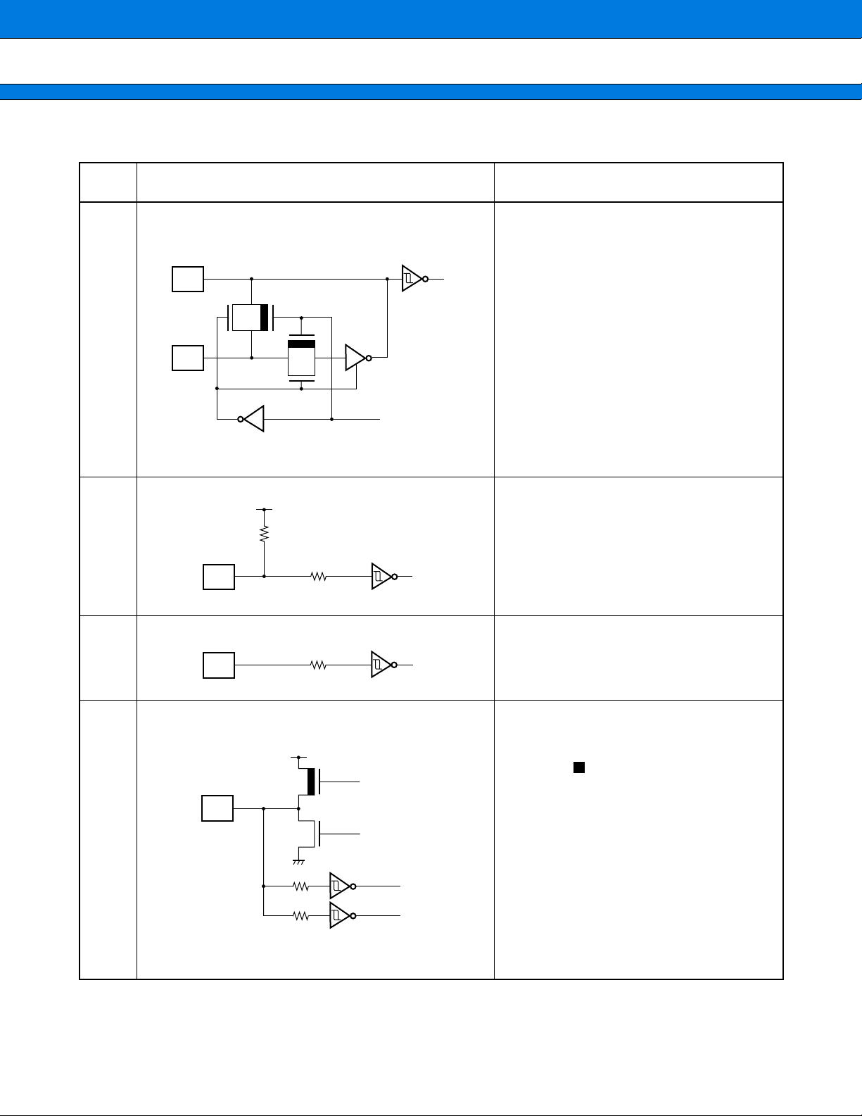
I/O CIRCUIT TYPE
■
Circuit
type
A
B
X1, X1A
X0,X0A
Circuit Remarks
• Oscillation feedback resistor :
1 MΩ approx. (High speed oscillator)
10MΩ approx. (Low speed oscillator)
osillation feedback
resistor
Standby control signal
• CMOS hysteresis input .
Pull-up resistor : 50 kΩ approx.
R (pull-up)
R
HYS
• CMOS hysteresis input
C
R
HYS
• CMOS level output
• CMOS hysteresis input
CC
V
P-ch
N-ch
• Automotive hysteresis input
(See “ INPUT LEVELS”.)
D
R
R
CMOS HYS
AUTOM. HYS
(Continued)
12
Page 13
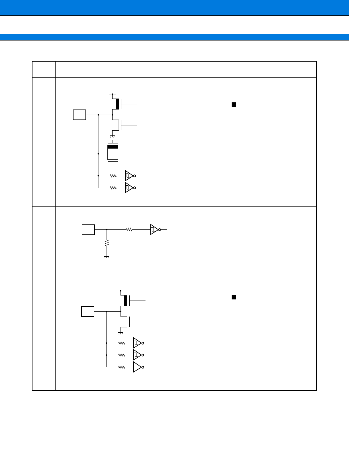
MB90440G Series
Circuit
type
E
Circuit Remarks
• CMOS level output
CC
V
P-ch
• CMOS hysteresis input
• Automotive hysteresis input
(See “ INPUT LEVELS”.)
• Analog input
N-ch
P-ch
Analog input
N-ch
R
R
CMOS HYS
AUTOM. HYS
• CMOS hysteresis input
R
CMOS HYS
• Pull-down resistor : 50 kΩ approx.
(except FLASH devices)
F
R (pull-down)
• CMOS level output
• CMOS hysteresis input
CC
V
P-ch
• Automotive hysteresis input
(See “ INPUT LEVELS”.)
• TTL input (FLASH devices in flash write
mode only)
N-ch
G
R
R
R
T
CMOS HYS
AUTOM. HYS
TTL
(Continued)
13
Page 14
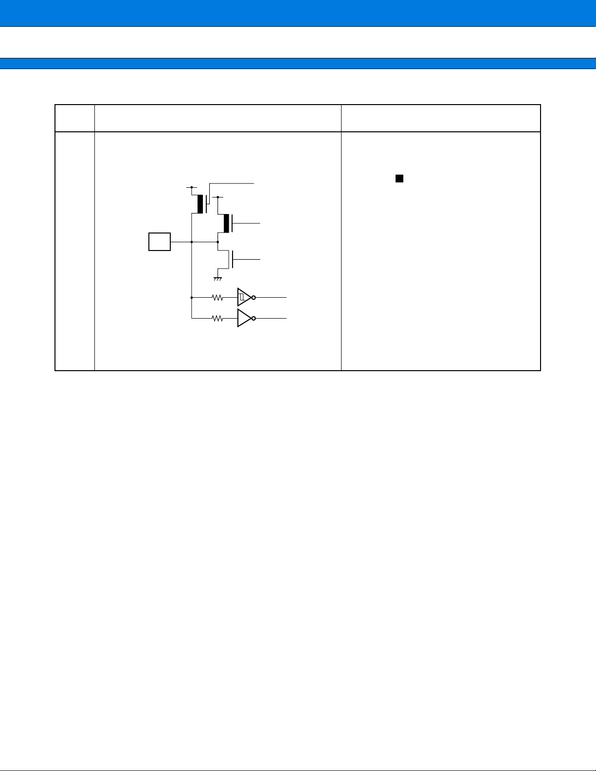
MB90440G Series
(Continued)
Circuit
type
Circuit Remarks
VCC
• CMOS level output
• CMOS hysteresis input
• TTL hysteresis input
CNTL
CC
V
P-ch
(See “ INPUT LEVELS”.)
• Programmable pullup resistor :
50 kΩ approx.
H
R
R
N-ch
CMOS HYS
T
TTL
14
Page 15
MB90440G Series
HANDLING DEVICES
■
1. Preventing Latch-up
CMOS IC chips may suffer latch-up under the following conditions :
(1) A voltage higher than V
(2) A voltage higher than the rated voltage is applied to between V
(3) The AV
CC power supply is applied before the VCC voltage.
Latch-up may increase the power supply current drastically, causing thermal damage to the device.
Always take sufficient precautions in using semiconductor devices to avoid this possibility.
Also be careful not to let the analog power-supply voltage (AV
(V
CC) when the analog system power-supply is turned on and off.
2. Handling Unused Input Pins
Do not leave unused input pins open, as doing so may cause misoperation of the device or latch-up leading to
permanent damage. Unused input pins should be pulled up or pulled down through at least 2 kΩ resistance.
Unused I/O pins may be left open in output state, but if such pins are in input state they should be handled in
the same way as input pins.
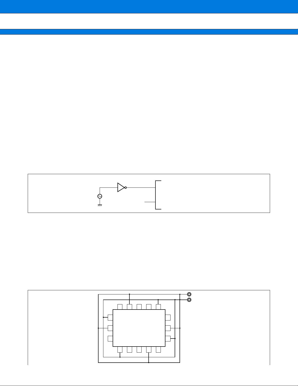
3. Use of the External Clock
To use the external clock, drive only the X0 pin and leave the X1 pin open.
A diagram of how to use an external clock is shown below.
CC or lower than VSS is applied to an input or output pin.
CC and Vss.
CC, A VRH) exceed the digital po wer-supply voltage
MB90440G Series
X0
X1open
4. Precautions for when not using a Sub Clock Signal
If the X0A and X1A pins are not connected to an oscillator, apply pull-do wn treatment to the X0A pin and leave
the X1A pin open.
5. Power Supply Pins (VCC/VSS)
In products with multiple VCC or VSS pins, the pins of a same potential are internally connected in the device to
avoid abnormal operations including latch-up. However, connect the pins exter nal power and ground lines to
lower the electro-magnetic emission level to prevent abnormal operation of strobe signals caused by the rise in
the ground level, and to conform to the total current rating.
Make sure to connect V
It is recommended to provide a bypass capacitor of around 0.1 µF between V
CC and VSS pins via lowest impedance to power lines.
VCC
VSS
VSS
VCC
VCC
MB90440G
Series
VSS
VCC
CC and VSS pins near the device.
VSS
VSS
VCC
15
Page 16

MB90440G Series
6. Pull-up/down resistors
The MB90440G Series does not support inter nal pull-up/down resistors (except pull-up resistors of port 0 to
port 3) . Use external components needed.
7. Crystal Oscillator Circuit
Noises around X0 or X1 pins may cause abnormal operations. Make sure to pro vide bypass capacitors via the
shortest distances from X0 and X1 pins, cr ystal oscillator (or ceramic resonator) and ground lines, and make
sure, to the utmost effort, that lines of oscillation circuits do not cross the lines of other circuits.
It is highly recommended to provide a printed circuit board artwork surrounding X0 and X1 pins with a ground
area for stabilizing the operation.
8. Turning-on Sequence of Power Supply to A/D Converter and Analog Inputs
Make sure to turn on the A/D and D/A converters power supply (AVCC, AVRH, AVRL) and analog inputs (AN0 to
AN7) after turning on the digital power supply (V
Turn off the digital power after turning off the A/D converter supply and analog inputs. In this case, make sure
that A VRH does not exceed AV
able) .
CC (turning on/off the analog and digital power supplies simultaneously is accept-
9. Connection of Unused Pins of A/D Converter
Connect unused pins of A/D and D/A converters to AVCC = VCC, AVSS = AVRH = VSS.
CC) .
10. N.C. Pin
The N.C. (internally connected) pin must be opened for use.
11. Notes on Energization
To prevent the internal regulator circuit from malfunctioning, set the voltage rise time during energization at 50
µs or more (0.2 V to 2.7 V) .
12. Initialization
In the device, there are internal registers which are initialized only by a pow er-on reset. T o initialize these registers,
please turn on the power again.
13. Using REALOS
The use of (EI2OS) is not possible with the REALOS real time operation system.
14. Caution on Operations during PLL Clock Mode
If the PLL clock mode is selected in the microcontroller , it may attempt to continue the operation using the freerunning frequency of the automatic oscillating circuit in the PLL circuitly even if the oscillator is out of place or
the clock input is stopped. Performance of this operation, however, cannot be guaranteed.
16
Page 17
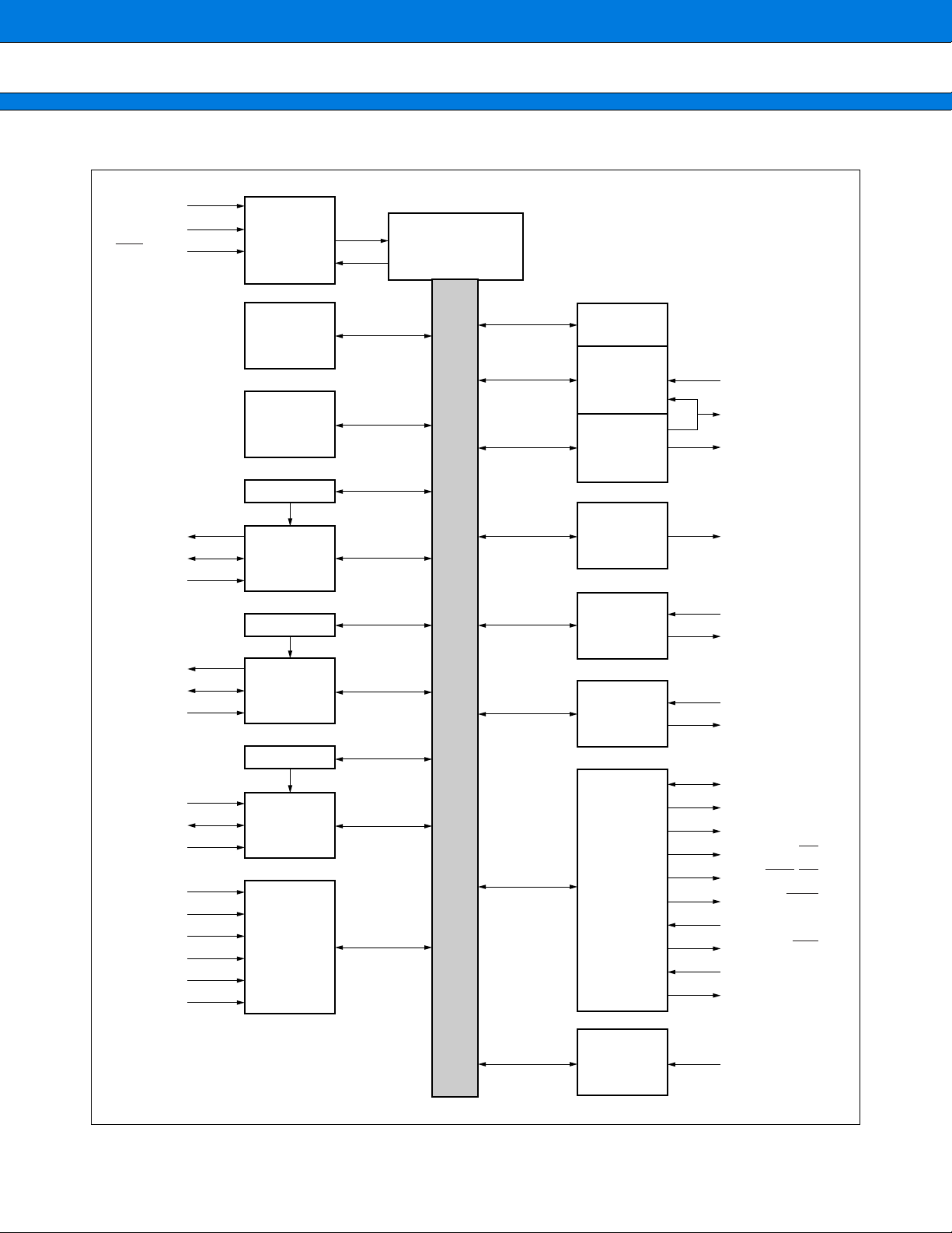
BLOCK DIAGRAM
■
X0, X1
X0A, X1A
RST
Clock
Controller
RAM 6 K
MB90440G Series
F2MC 16LX
CPU
16 bit
I/O Timer
SOT0
SCK0
SIN0
SOT1
SCK1
SIN1
SCK2
SOT2
SIN2
AV
CC
AVSS
AN0 to AN7
AVRH
AVRL
ADTG
ROM
128 K
Prescaler
UART0
Prescaler
UART1
(SCI)
Prescaler
Serial I/O
10-bit ADC
8 ch
2
F MC-16 Bus
16 bit Input
Capture
8 ch
16 bit Output
Compare
4 ch
8/16-bit
PPG Timer
4 ch
CAN
Controller 3 ch
16-bit Reload
Timer 2 ch
External
Bus
Interface
IN0 to IN5
IN6/OUT2,
IN7/OUT3
OUT0, OUT1
PPG0 to PPG3
RX0 to RX2
TX0 to TX2
TIN0, TIN1
TOT0, T O T1
AD00 to AD15
A16 to A23
ALE
RD
WRL/WR
WRH
HRQ
HAK
RDY
CLK
External
Interrupt
Circuit 8 ch
INT0 to INT7
17
Page 18
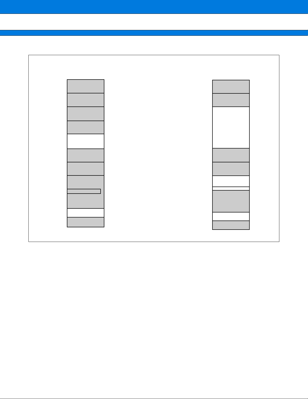
MB90440G Series
MEMORY MAP
■
MB90V440G MB90F443G/
MB90443G (under development)
FFFFFF
FF0000H
FEFFFFH
FE0000H
FDFFFFH
FD0000H
FCFFFFH
FC0000H
00FFFFH
004000H
003FFFH
003900H
0038FFH
001FF5H
001FF0H
000100H
0000BFH
000000H
H
ROM (FF bank)
ROM (FE bank)
ROM (FD bank)
ROM (FC bank)
External
Access Memory
ROM (Image of
FF bank)
Peripheral
ROM correction
RAM 14 K
External
Access Memory
Peripheral
FFFFFF
FF0000H
FEFFFFH
FE0000H
00FFFFH
004000H
003FFFH
003900H
002000H
0018FFH
000100H
0000BFH
000000H
H
ROM (FF bank)
ROM (FE bank)
External
Access Memory
ROM (Image of
FF bank)
Peripheral
External
Access Memory
RAM 6 K
External
Access Memory
Peripheral
Note : The high-order portion of bank 00 gives the image of the FF bank ROM to make the small model of the C
compiler effective. Since the low-order 16 bits are the same address, the table in ROM can be referenced
without using the far specification in the pointer declaration.
For example, an attempt to access 00C000
H accesses the value at FFC000H in ROM.
The ROM area in bank FF exceeds 48 Kbytes, and its entire image cannot be shown in bank 00.
The image between FF4000
FFFFFF
of FF4000
H is visible only in bank FF. Thus, it is recommended that the ROM data table be stored in the area
H and FFFFFFH .
H and FFFFFFH is visible in bank 00, while the image between FF4000H and
18
Page 19

I/O MAP
■
MB90440G Series
Address Register Abbreviation
00
H Port 0 data register PDR0 R/W Port 0 XXXXXXXXB
01H Port 1 data register PDR1 R/W Port 1 XXXXXXXXB
02H Port 2 data register PDR2 R/W Port 2 XXXXXXXXB
03H Port 3 data register PDR3 R/W Port 3 XXXXXXXXB
04H Port 4 data register PDR4 R/W Port 4 XXXXXXXXB
05H Port 5 data register PDR5 R/W Port 5 XXXXXXXXB
06H Port 6 data register PDR6 R/W Port 6 XXXXXXXXB
07H Port 7 data register PDR7 R/W Port 7 XXXXXXXXB
08H Port 8 data register PDR8 R/W Port 8 XXXXXXXXB
09H Port 9 data register PDR9 R/W Port 9 XXXXXXXXB
0AH Port A data register PDRA R/W Port A _______XB
0BH Port input levels select register PILR R/W Ports 00000000B
0CH CAN2 RX/TX pin switching register CANSWR R/W CAN1/2 ______00B
0DH to 0FH Reserved
10
H Port 0 direction register DDR0 R/W Port 0 00000000B
11H Port 1 direction register DDR1 R/W Port 1 00000000B
Read/
Write
Resource
name
Initial value
12H Port 2 direction register DDR2 R/W Port 2 00000000B
13H Port 3 direction register DDR3 R/W Port 3 00000000B
14H Port 4 direction register DDR4 R/W Port 4 00000000B
15H Port 5 direction register DDR5 R/W Port 5 00000000B
16H Port 6 direction register DDR6 R/W Port 6 00000000B
17H Port 7 direction register DDR7 R/W Port 7 00000000B
18H Port 8 direction register DDR8 R/W Port 8 00000000B
19H Port 9 direction register DDR9 R/W Port 9 00000000B
1AH Port A direction register DDRA R/W Port A _______0B
1BH Analog input enable register ADER R/W Port 6, A/D 11111111B
1CH Port 0 pullup control register PUCR0 R/W Port 0 00000000B
1DH Port 1 pullup control register PUCR1 R/W Port 1 00000000B
1EH Port 2 pullup control register PUCR2 R/W Port 2 00000000B
1FH Port 3 pullup control register PUCR3 R/W Port 3 00000000B
20H Serial mode control register 0 UMC0 R/W
21H Serial status register 0 USR0 R/W 00010000B
UART0
22H Serial input/output data register 0 UIDR0/UODR0 R/W XXXXXXXXB
23H Rate and data register 0 URD0 R/W 0000000XB
00000100B
(Continued)
19
Page 20
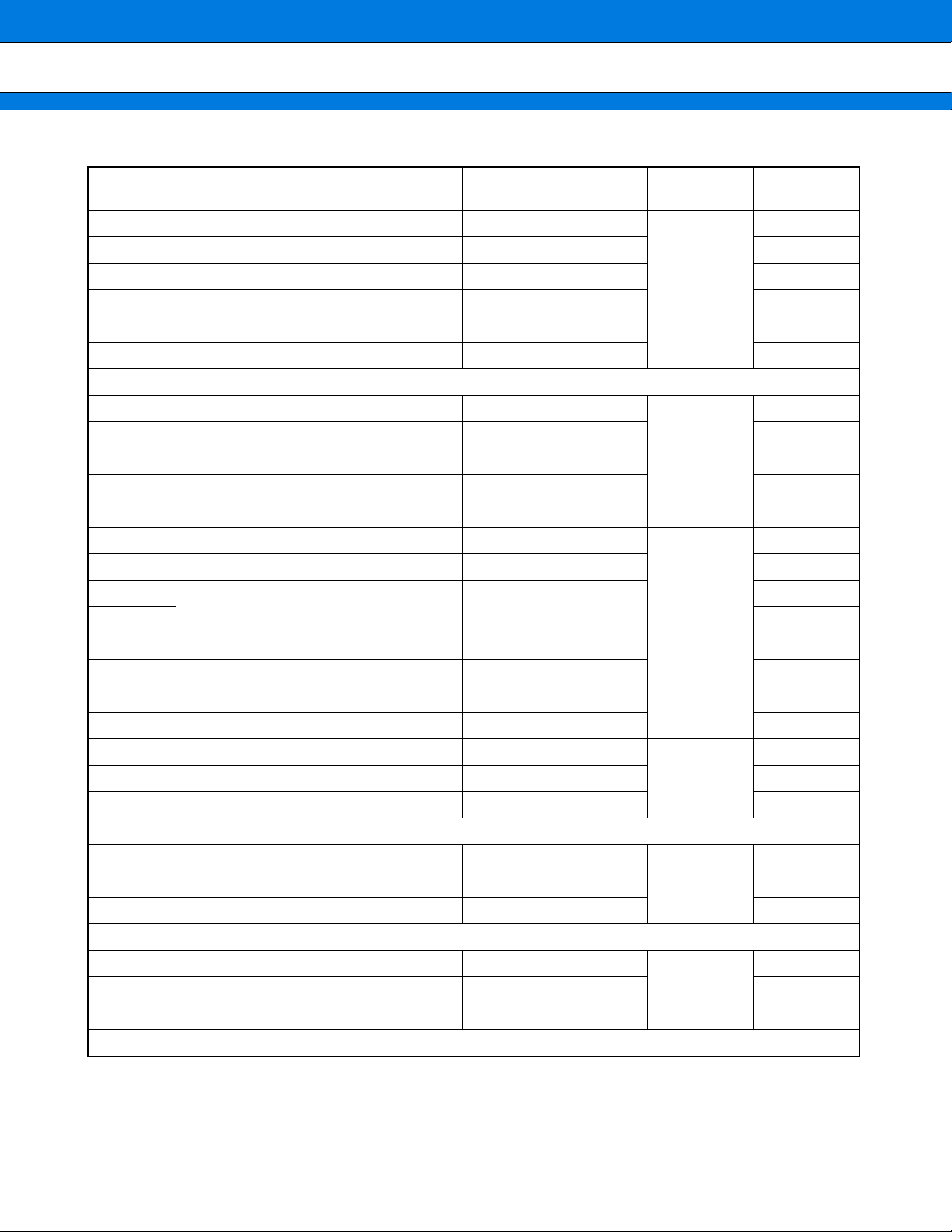
MB90440G Series
Address Register Abbreviation
24
H Serial mode register 1 SMR1 R/W
Read/
Write
Resource
name
Initial value
00000000B
25H Serial control register 1 SCR1 R/W 00000100B
26H Serial input/output data register 1 SIDR1/SODR1 R/W XXXXXXXXB
UART1
27H Serial status register 1 SSR1 R/W 00001_00B
28H UART1 prescaler control register U1CDCR R/W 0___1111B
29H Serial edge selection registor SES1 R/W _______0B
2AH Reserved
2BH Serial I/O prescaler SCDCR R/W
0___1111B
2CH Serial mode control register SMCS R/W ____0000B
2DH Serial mode control register SMCS R/W 00000010B
Serial I/O
2EH Serial Data register SDR R/W XXXXXXXXB
2FH Serial edge selection registor 2 SES2 R/W _______0B
30H External interrupt enable register ENIR R/W
31H External interrupt request register EIRR R/W XXXXXXXXB
External
00000000B
interrupt
32H
External request level setting register ELVR R/W
circuit
00000000
33H 00000000B
B
34H A/D control status register 0 ADCS0 R/W
35H A/D control status register 1 ADCS1 R/W 00000000B
36H A/D data register 0 ADCR0 R XXXXXXXXB
A/D
converter
00000000B
37H A/D data register 1 ADCR1 R/W 00001_XXB
38H PPG0 operation mode control register PPGC0 R/W
39H PPG1 operation mode control register PPGC1 R/W 0_000001B
3AH PPG0 and PPG1 clock selection register PPG01 R/W 000000__B
16-bit Progra-
mable Pulse
Generator 0/1
0_000__1B
3BH Reserved
3C
H PPG2 operation mode control register PPGC2 R/W
3DH PPG3 operation mode control register PPGC3 R/W 0_000001B
3EH PPG2 and PPG3 clock selection register PPG23 R/W 000000__B
16-bit Progra-
mable Pulse
Generator 2/3
0_000__1B
3FH Reserved
40
H PPG4 operation mode control register PPGC4 R/W
41H PPG5 operation mode control register PPGC5 R/W 0_000001B
42H PPG4 and PPG5 clock selection register PPG45 R/W 000000__B
16-bit Progra-
mable Pulse
Generator 4/5
0_000__1B
43H Reserved
(Continued)
20
Page 21

MB90440G Series
Address Register
44
H PPG6 operation mode control register PPGC6 R/W 16-bit
Abbrevia-
tion
45H PPG7 operation mode control register PPGC7 R/W 0_000001B
46H PPG6 and PPG7 clock selection register PPG67 R/W 000000__B
Read/
Write
Resource
name
Programable
Pulse
Generator 6/7
Initial value
0_000__1B
47H to 4BH Reserved
4C
H Input capture control status 0/1 ICS01 R/W Input capture 0/1 00000000B
4DH Input capture control status 2/3 ICS23 R/W Input capture 2/3 00000000B
4EH Input capture control status 4/5 ICS45 R/W Input capture 4/5 00000000B
4FH Input capture control status 6/7 ICS67 R/W Input capture 6/7 00000000B
50H
51H ____0000B
Timer control status register 0 TMCSR0 R/W
16-bit
00000000
reload
52H
Timer register 0/reload register 0
53H XXXXXXXXB
TMR0/
TMRLR0
R/W
timer 0
54H
XXXXXXXX
00000000
Timer control status register 1 TMCSR1 R/W
55H ____0000B
56H
Timer register 1/Reload register 1
57H XXXXXXXXB
TMR1/
TMRLR1
R/W
16-bit reload
timer 1
XXXXXXXX
B
B
B
B
58H Output compare control status register 0 OCS0 R/W
59H Output compare control status register 1 OCS1 R/W ___00000B
5AH Output compare control status register 2 OCS2 R/W
5BH Output compare control status register 3 OCS3 R/W ___00000B
Output
compare 0/1
Output
compare 2/3
0000__00B
0000__00B
5CH to 6BH Reserved for CAN 2 Interface
6C
H
00000000
Timer data register TCDT R/W
6DH 00000000B
I/O timer
6EH Timer control status register TCCS R/W 00000000B
ROM mirror
6FH ROM mirror function selection register ROMM R/W
function selec-
_______1B
tion module
70H to 7FH Reserved for CAN 0 Interface
80
H to 8FH Reserved for CAN 1 Interface
90
H to 9DH Prohibited area
Address match
detection
function
00000000B
9EH
Program address detection control
status register
PACSR R/W
Delayed
9FH Delayed interrupt/release register DIRR R/W
interrupt genera-
_______0B
tion module
(Continued)
B
21
Page 22

MB90440G Series
Address Register Abbreviation
A0
H
Low-power consumption mode
control register
LPMCR R/W
Read/
Write
Resource name Initial value
Low power
consumption
00011000B
(stand-by) mode
Low power
A1H Clock selection register CKSCR R/W
consumption
11111100B
(stand-by) mode
A2H to A4H Prohibited area
A5H
A6H
Automatic ready function select
register
External address output control
register
ARSR W
HACR W 00000000B
External bus pin
0011__00B
A7H Bus control signal selection register ECSR W 0000000_B
A8H Watchdog timer control register WDTC R/W
A9H Time base timer control register TBTC R/W
Watchdog
timer
Time base
timer
XXXXX111B
1- -00100B
AAH Watch timer control register WTC R/W Watch timer 1X000000B
ABH to ADH Prohibited area
AE
Flash memory control status register
H
(Flash only, otherwise reserved)
FMCS R/W Flash Memory 000X0000B
AFH Prohibited area
B0
H Interrupt control register 00 ICR00 R/W
00000111B
B1H Interrupt control register 01 ICR01 R/W 00000111B
B2H Interrupt control register 02 ICR02 R/W 00000111B
B3H Interrupt control register 03 ICR03 R/W 00000111B
B4H Interrupt control register 04 ICR04 R/W 00000111B
B5H Interrupt control register 05 ICR05 R/W 00000111B
B6H Interrupt control register 06 ICR06 R/W 00000111B
B7H Interrupt control register 07 ICR07 R/W 00000111B
B8H Interrupt control register 08 ICR08 R/W 00000111B
Interrupt
controller
B9H Interrupt control register 09 ICR09 R/W 00000111B
BAH Interrupt control register 10 ICR10 R/W 00000111B
BBH Interrupt control register 11 ICR11 R/W 00000111B
BCH Interrupt control register 12 ICR12 R/W 00000111B
BDH Interrupt control register 13 ICR13 R/W 00000111B
BEH Interrupt control register 14 ICR14 R/W 00000111B
BFH Interrupt control register 15 ICR15 R/W 00000111B
COH to FFH External
22
(Continued)
Page 23

(Continued)
Address Register Abbreviation
1FF0
H
MB90440G Series
Read/
Write
R/W
Resource name Initial value
XXXXXXXX
B
1FF1H R/W XXXXXXXXB
1FF2H R/W XXXXXXXXB
1FF3H
1FF4H R/W XXXXXXXXB
Program address detection register 0 PADR0
Program address detection register 1 PADR1
Address match
R/W XXXXXXXXB
detection function
1FF5H R/W XXXXXXXXB
Address Register Abbreviation
3900
H Reload register L PRLL0 R/W
3901H Reload register H PRLH0 R/W XXXXXXXXB
Read/
Write
Resource name Initial value
XXXXXXXX
16-bit programable
pulse
3902H Reload register L PRLL1 R/W XXXXXXXXB
generator 0/1
3903H Reload register H PRLH1 R/W XXXXXXXXB
3904H Reload register L PRLL2 R/W
3905H Reload register H PRLH2 R/W XXXXXXXXB
16-bit programable
XXXXXXXXB
pulse
3906H Reload register L PRLL3 R/W XXXXXXXXB
generator 2/3
3907H Reload register H PRLH3 R/W XXXXXXXXB
3908H Reload register L PRLL4 R/W
3909H Reload register H PRLH4 R/W XXXXXXXXB
16-bit programable
XXXXXXXXB
pulse
390AH Reload register L PRLL5 R/W XXXXXXXXB
generator 4/5
390BH Reload register H PRLH5 R/W XXXXXXXXB
B
390CH Reload register L PRLL6 R/W
390DH Reload register H PRLH6 R/W XXXXXXXXB
16-bit programable
XXXXXXXXB
pulse
390EH Reload register L PRLL7 R/W XXXXXXXXB
generator 6/7
390FH Reload register H PRLH7 R/W XXXXXXXXB
3910H to
3917
H
3918H Input capture register 0 IPCP0 R
Reserved
XXXXXXXXB
3919H Input capture register 0 IPCP0 R XXXXXXXXB
Input captue 0/1
391AH Input capture register 1 IPCP1 R XXXXXXXXB
391BH Input capture register 1 IPCP1 R XXXXXXXXB
391CH Input capture register 2 IPCP2 R
XXXXXXXXB
391DH Input capture register 2 IPCP2 R XXXXXXXXB
Input captue 2/3
391EH Input capture register 3 IPCP3 R XXXXXXXXB
391FH Input capture register 3 IPCP3 R XXXXXXXXB
(Continued)
23
Page 24

MB90440G Series
(Continued)
Address Register Abbreviation
3920H Input capture register 4 IPCP4 R
3921H Input capture register 4 IPCP4 R XXXXXXXXB
3922H Input capture register 5 IPCP5 R XXXXXXXXB
3923H Input capture register 5 IPCP5 R XXXXXXXXB
3924H Input capture register 6 IPCP6 R
3925H Input capture register 6 IPCP6 R XXXXXXXXB
3926H Input capture register 7 IPCP7 R XXXXXXXXB
3927H Input capture register 7 IPCP7 R XXXXXXXXB
3928H Output compare register 0 OCCP0 R/W
3929H Output compare register 0 OCCP0 R/W XXXXXXXXB
392AH Output compare register 1 OCCP1 R/W XXXXXXXXB
392BH Output compare register 1 OCCP1 R/W XXXXXXXXB
392CH Output compare register 2 OCCP2 R/W
392DH Output compare register 2 OCCP2 R/W XXXXXXXXB
392EH Output compare register 3 OCCP3 R/W XXXXXXXXB
392FH Output compare register 3 OCCP3 R/W XXXXXXXXB
3930H to
39FF
H
3A00
H to
3AFF
H
3B00
H to
3BFF
H
3C00
H to
3CFF
H
3D00
H to
3DFF
H
3E00
H to
3EFF
H
3F00
H to
3FFF
H
Reserved for CAN 0 Interface
Reserved for CAN 0 Interface
Reserved for CAN 1 Interface
Reserved for CAN 1 Interface
Reserved for CAN 2 Interface
Reserved for CAN 2 Interface
Reserved
• Meaning of abbreviations used for reading and writing
R/W : Read and Write enabled
R : Read only
W : Write only
• Explanation of initial values
0 : The bit is initialized to 0.
1 : The bit is initialized to 1.
X : The initial value of the bit is undefined.
_ : The bit is not used. Its initial value is undefined.
Read/
Write
Resource name Initial value
XXXXXXXXB
Input captue 4/5
XXXXXXXXB
Input captue 6/7
XXXXXXXXB
Output compare 0/1
XXXXXXXXB
Output compare 2/3
Note : Addresses in the range 0000
of the MCU. A read access to these reserved addresses results reading “X” and any write access should
not be performed.
24
H to 00FFH, which are not listed in the table, are reserved for the primary functions
Page 25

MB90440G Series
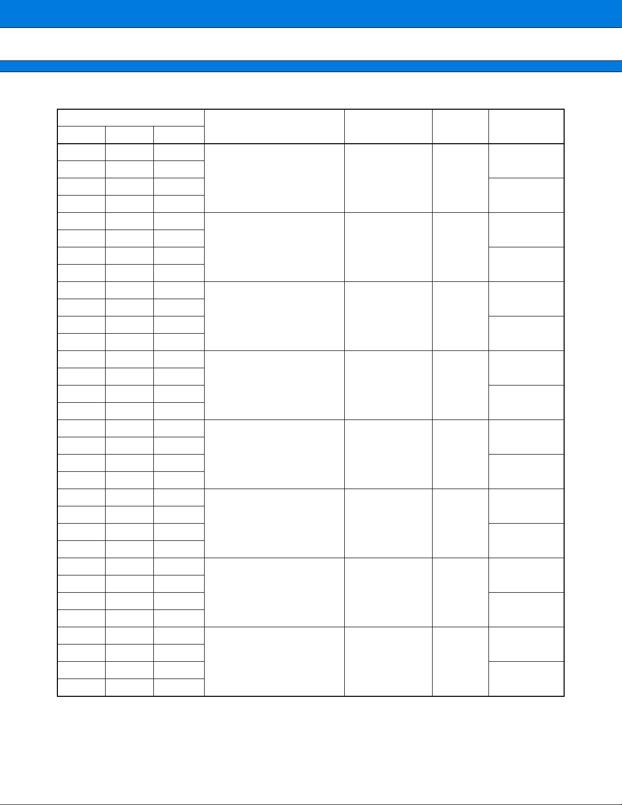
CAN CONTROLLER
■
The MB90440G series contains three generic CAN controllers (CAN0, CAN1, CAN2) .
The CAN controller has the following features
:
• Conforms to CAN Specification Version 2.0 Part A and B
- Supports transmission/reception in standard frame and extended frame formats
• Supports transmission of data frames by receiving remote frames
• 16 transmission/reception message buffers
- 29-bit ID and 8-byte data
- Multi-level message buffer configuration
• Provides full-bit comparison, full-bit mask, acceptance register 0/acceptance register 1 for each message
buffer as ID acceptance mask
- Two acceptance mask registers in either standard frame format or extended frame formats
• Bit rate programmable from 10 Kbps to 1 Mbps (when input clock is at 16 MHz)
List of Control Registers
Address
CAN0 CAN1 CAN2
000070
H 000080H 00005CH
000071H 000081H 00005DH
000072H 000082H 00005EH
000073H 000083H 00005FH
000074H 000084H 000060H
000075H 000085H 000061H
Register Abbreviation
Message buffer valid register BVALR R/W
Transmit request register TREQR R/W
Transmit cancel register TCANR W
Read/
Write
Initial Value
00000000
00000000B
00000000
00000000B
00000000
00000000B
000076H 000086H 000062H
000077H 000087H 000063H
000078H 000088H 000064H
000079H 000089H 000065H
00007AH 00008AH 000066H
00007BH 00008BH 000067H
00007CH 00008CH 000068H
00007DH 00008DH 000069H
00007EH 00008EH 00006AH
00007FH 00008FH 00006BH
003B00H 003D00H 003F00H
003B01H 003D01H 003F01H
003B02H 003D02H 003F02H
003B03H 003D03H 003F03H
003B04H 003D04H 003F04H
003B05H 003D05H 003F05H
Transmit complete register TCR R/W
Receive complete register RCR R/W
Remote request receiving
register
RRTRR R/W
Receive overrun register ROVRR R/W
Receive interrupt enable
register
RIER R/W
Control status register CSR R/W, R
Last event indicator register LEIR R/W
Receive/transmit error
counter
RTEC R
00000000
00000000B
00000000
00000000B
00000000
00000000
B
00000000
00000000B
00000000
00000000
B
00---000 0----0-
1B
-------- 0000000B
00000000
00000000
B
(Continued)
25
Page 26

MB90440G Series
(Continued)
Address
CAN0 CAN1 CAN2
003B06
003B07H 003D07H 003F07H
H 003D06H 003F06H
Register Abbreviation
Read/
Write
Bit timing register BTR R/W
Initial Value
-1111111
11111111B
003B08H 003D08H 003F08H
003B09H 003D09H 003F09H
003B0AH 003D0AH 003F0AH
003B0BH 003D0BH 003F0BH
003B0CH 003D0CH 003F0CH
003B0DH 003D0DH 003F0DH
003B0EH 003D0EH 003F0EH
003B0FH 003D0FH 003F0FH
003B10H 003D10H 003F10H
003B11H 003D11H 003F11H
003B12H 003D12H 003F12H
003B13H 003D13H 003F13H
003B14H 003D14H 003F14H
003B15H 003D15H 003F15H
003B16H 003D16H 003F16H
003B17H 003D17H 003F17H
003B18H 003D18H 003F18H
003B19H 003D19H 003F19H
003B1AH 003D1AH 003F1AH
003B1BH 003D1BH 003F1BH
IDE register IDER R/W
Transmit RTR register TRTRR R/W
Remote frame receive waiting
register
Transmit interrupt enable
register
Acceptance mask select
register
RFWTR R/W
TIER R/W
AMSR R/W
Acceptance mask register 0 AMR0 R/W
Acceptance mask register 1 AMR1 R/W
XXXXXXXX
XXXXXXXXB
00000000
00000000B
XXXXXXXX
XXXXXXXX
00000000
00000000
B
XXXXXXXX
XXXXXXXX
XXXXXXXX
XXXXXXXX
XXXXXXXX
XXXXXXXX
XXXXX---
XXXXXXXX
XXXXXXXX
XXXXXXXX
XXXXX---
XXXXXXXX
B
B
B
B
B
B
B
26
Page 27

MB90440G Series
Address
CAN0 CAN1 CAN2
003A00
003A1F
to
H
003C00H
003C1F
H
to
003E00H
003E1F
H
to
003A20H 003C20H 003E20H
003A21H 003C21H 003E21H
003A22H 003C22H 003E22H
003A23H 003C23H 003E23H
003A24H 003C24H 003E24H
003A25H 003C25H 003E25H
003A26H 003C26H 003E26H
003A27H 003C27H 003E27H
003A28H 003C28H 003E28H
003A29H 003C29H 003E29H
003A2AH 003C2AH 003E2AH
003A2BH 003C2BH 003E2BH
003A2CH 003C2CH 003E2CH
003A2DH 003C2DH 003E2DH
003A2EH 003C2EH 003E2EH
003A2FH 003C2FH 003E2FH
003A30H 003C30H 003E30H
003A31H 003C31H 003E31H
003A32H 003C32H 003E32H
003A33H 003C33H 003E33H
List of Message Buffers (ID Registers
Register Abbreviation
RAM area R/W
H
ID register 0 IDR0 R/W
ID register 1 IDR1 R/W
ID register 2 IDR2 R/W
ID register 3 IDR3 R/W
ID register 4 IDR4 R/W
)
Read/
Write
Initial Value
XXXXXXXX
B
to
XXXXXXXX
B
XXXXXXXX
XXXXXXXXB
XXXXX---
XXXXXXXX
B
XXXXXXXX
XXXXXXXX
B
XXXXX---
XXXXXXXX
B
XXXXXXXX
XXXXXXXX
B
XXXXX---
XXXXXXXX
B
XXXXXXXX
XXXXXXXX
B
XXXXX---
XXXXXXXX
B
XXXXXXXX
XXXXXXXXB
XXXXX---
XXXXXXXX
B
003A34H 003C34H 003E34H
003A35H 003C35H 003E35H
003A36H 003C36H 003E36H
003A37H 003C37H 003E37H
003A38H 003C38H 003E38H
003A39H 003C39H 003E39H
003A3AH 003C3AH 003E3AH
003A3BH 003C3BH 003E3BH
ID register 5 IDR5 R/W
ID register 6 IDR6 R/W
XXXXXXXX
XXXXXXXX
XXXXX---
XXXXXXXX
XXXXXXXX
XXXXXXXX
XXXXX---
XXXXXXXX
(Continued)
B
B
B
B
27
Page 28
MB90440G Series
Address
CAN0 CAN1 CAN2
003A3C
H 003C3CH 003E3CH
003A3DH 003C3DH 003E3DH
003A3EH 003C3EH 003E3EH
003A3FH 003C3FH 003E3FH
003A40H 003C40H 003E40H
003A41H 003C41H 003E41H
003A42H 003C42H 003E42H
003A43H 003C43H 003E43H
003A44H 003C44H 003E44H
003A45H 003C45H 003E45H
003A46H 003C46H 003E46H
003A47H 003C47H 003E47H
003A48H 003C48H 003E48H
003A49H 003C49H 003E49H
003A4AH 003C4AH 003E4AH
003A4BH 003C4BH 003E4BH
Register Abbreviation
Read/
Write
ID register 7 IDR7 R/W
ID register 8 IDR8 R/W
ID register 9 IDR9 R/W
ID register 10 IDR10 R/W
Initial Value
XXXXXXXX
XXXXXXXX
XXXXX---
XXXXXXXX
XXXXXXXX
XXXXXXXXB
XXXXX---
XXXXXXXX
XXXXXXXX
XXXXXXXX
XXXXX---
XXXXXXXX
XXXXXXXX
XXXXXXXX
XXXXX---
XXXXXXXX
B
B
B
B
B
B
B
003A4CH 003C4CH 003E4CH
003A4DH 003C4DH 003E4DH
003A4EH 003C4EH 003E4EH
003A4FH 003C4FH 003E4FH
003A50H 003C50H 003E50H
003A51H 003C51H 003E51H
003A52H 003C52H 003E52H
003A53H 003C53H 003E53H
003A54H 003C54H 003E54H
003A55H 003C55H 003E55H
003A56H 003C56H 003E56H
003A57H 003C57H 003E57H
003A58H 003C58H 003E58H
003A59H 003C59H 003E59H
003A5AH 003C5AH 003E5AH
003A5BH 003C5BH 003E5BH
ID register 11 IDR11 R/W
ID register 12 IDR12 R/W
ID register 13 IDR13 R/W
ID register 14 IDR14 R/W
XXXXXXXX
XXXXXXXX
XXXXX---
XXXXXXXX
XXXXXXXX
XXXXXXXXB
XXXXX---
XXXXXXXX
XXXXXXXX
XXXXXXXX
XXXXX---
XXXXXXXX
XXXXXXXX
XXXXXXXX
XXXXX---
XXXXXXXX
(Continued)
B
B
B
B
B
B
B
28
Page 29

(Continued)
Address
CAN0 CAN1 CAN2
003A5C
H 003C5CH 003E5CH
003A5DH 003C5DH 003E5DH
003A5EH 003C5EH 003E5EH
003A5FH 003C5FH 003E5FH
MB90440G Series
Register Abbreviation
ID register 15 IDR15 R/W
Read/
Write
Initial Value
XXXXXXXX
XXXXXXXX
XXXXX---
XXXXXXXX
B
B
List of Message Buffers (DLC Registers and Data Registers
Address
CAN0 CAN1 CAN2
003A60
H 003C60H 003E60H
003A61H 003C61H 003E61H
003A62H 003C62H 003E62H
003A63H 003C63H 003E63H
003A64H 003C64H 003E64H
003A65H 003C65H 003E65H
003A66H 003C66H 003E66H
003A67H 003C67H 003E67H
003A68H 003C68H 003E68H
003A69H 003C69H 003E69H
003A6AH 003C6AH 003E6AH
003A6BH 003C6BH 003E6BH
003A6CH 003C6CH 003E6CH
003A6DH 003C6DH 003E6DH
003A6EH 003C6EH 003E6EH
003A6FH 003C6FH 003E6FH
003A70H 003C70H 003E70H
003A71H 003C71H 003E71H
)
Register Abbreviation
Read/
Write
Initial Value
DLC register 0 DLCR0 R/W ----XXXXB
DLC register 1 DLCR1 R/W ----XXXXB
DLC register 2 DLCR2 R/W ----XXXXB
DLC register 3 DLCR3 R/W ----XXXXB
DLC register 4 DLCR4 R/W ----XXXXB
DLC register 5 DLCR5 R/W ----XXXXB
DLC register 6 DLCR6 R/W ----XXXXB
DLC register 7 DLCR7 R/W ----XXXXB
DLC register 8 DLCR8 R/W ----XXXXB
003A72H 003C72H 003E72H
003A73H 003C73H 003E73H
003A74H 003C74H 003E74H
003A75H 003C75H 003E75H
003A76H 003C76H 003E76H
003A77H 003C77H 003E77H
DLC register 9 DLCR9 R/W ----XXXXB
DLC register 10 DLCR10 R/W ----XXXXB
DLC register 11 DLCR11 R/W ----XXXXB
(Continued)
29
Page 30

MB90440G Series
Address
CAN0 CAN1 CAN2
003A78
H 003C78H 003E78H
003A79H 003C79H 003E79H
003A7AH 003C7AH 003E7AH
003A7BH 003C7BH 003E7BH
003A7CH 003C7CH 003E7CH
003A7DH 003C7DH 003E7DH
003A7EH 003C7EH 003E7EH
003A7FH 003C7FH 003E7FH
003A80H
to
003A87
003A88H
to
003A8F
003A90H
to
003A97
003C80H
003C87
H
003C88H
003C8F
H
003C90H
003C97
H
to
to
to
003E80H
003E87
H
003E88H
003E8F
H
003E90H
003E97
H
to
to
to
Register Abbreviation
DLC register 12 DLCR12 R/W ----XXXXB
DLC register 13 DLCR13 R/W ----XXXXB
DLC register 14 DLCR14 R/W ----XXXXB
DLC register 15 DLCR15 R/W ----XXXXB
Data register 0 (8 bytes) DTR0 R/W
H
Data register 1 (8 bytes) DTR1 R/W
H
Data register 2 (8 bytes) DTR2 R/W
H
Read/
Write
Initial Value
XXXXXXXX
to
XXXXXXXX
XXXXXXXX
to
XXXXXXXX
XXXXXXXX
to
XXXXXXXX
B
B
B
B
B
B
003A98H
to
003A9F
003AA0H
to
003AA7
003AA8H
to
003AAF
003AB0H
to
003AB7
003C98H
003C9F
H
003CA0H
003CA7
H
003CA8H
003CAF
H
003CB0H
003CB7
H
to
to
to
to
003E98H
003E9F
H
003EA0H
003EA7
H
003EA8H
003EAF
H
003EB0H
003EB7
H
to
to
to
to
Data register 3 (8 bytes) DTR3 R/W
H
Data register 4 (8 bytes) DTR4 R/W
H
Data register 5 (8 bytes) DTR5 R/W
H
Data register 6 (8 bytes) DTR6 R/W
H
XXXXXXXX
to
XXXXXXXX
XXXXXXXX
to
XXXXXXXX
XXXXXXXX
to
XXXXXXXX
XXXXXXXX
to
XXXXXXXX
(Continued)
B
B
B
B
B
B
B
B
30
Page 31

(Continued)
Address
CAN0 CAN1 CAN2
003AB8
003ABF
003AC0H
003AC7
to
to
H
003CB8H
003CBF
H
003CC0H
003CC7
H
to
to
003EB8H
003EBF
H
003EC0H
003EC7
H
to
to
MB90440G Series
Register Abbreviation
Data register 7 (8 bytes) DTR7 R/W
H
Data register 8 (8 bytes) DTR8 R/W
H
Read/
Write
Initial Value
XXXXXXXX
to
XXXXXXXX
XXXXXXXX
to
XXXXXXXX
B
B
B
B
003AC8H
to
003ACF
003AD0H
to
003AD7
003AD8H
to
003ADF
003AE0H
to
003AE7
003AE8H
to
003AEF
003AF0H
to
003AF7
003AF8H
to
003AFF
003CC8H
003CCF
H
003CD0H
003CD7
H
003CD8H
003CDF
H
003CE0H
003CE7
H
003CE8H
003CEF
H
003CF0H
003CF7
H
003CF8H
003CFF
H
to
to
to
to
to
to
to
003EC8H
003ECF
H
003ED0H
003ED7
H
003ED8H
003EDF
H
003EE0H
003EE7
H
003EE8H
003EEF
H
003EF0H
003EF7
H
003EF8H
003EFF
H
to
to
to
to
to
to
to
Data register 9 (8 bytes) DTR9 R/W
H
Data register 10 (8 bytes) DTR10 R/W
H
Data register 11 (8 bytes) DTR11 R/W
H
Data register 12 (8 bytes) DTR12 R/W
H
Data register 13 (8 bytes) DTR13 R/W
H
Data register 14 (8 bytes) DTR14 R/W
H
Data register 15 (8 bytes) DTR15 R/W
H
XXXXXXXX
to
XXXXXXXX
XXXXXXXX
to
XXXXXXXX
XXXXXXXX
to
XXXXXXXX
XXXXXXXX
to
XXXXXXXX
XXXXXXXX
to
XXXXXXXX
XXXXXXXX
to
XXXXXXXX
XXXXXXXX
to
XXXXXXXX
B
B
B
B
B
B
B
B
B
B
B
B
B
B
31
Page 32

MB90440G Series
INTERRUPT FACTORS, INTERRUPT VECTORS, INTERRUPT CONTROL REGISTER
■
Interrupt cause
2
OS
EI
support
Interrupt vector Interrupt control register
Number Address Number Address
Reset N/A #08 FFFFDC
INT9 instruction N/A #09 FFFFD8
Exception processing N/A #10 FFFFD4
CAN 0 Receive N/A #11 FFFFD0H
CAN 0 Transmit/Node status N/A #12 FFFFCCH
CAN 1 Receive N/A #13 FFFFC8H
CAN 1 Transmit/Node status N/A #14 FFFFC4H
External interrupt (INT0/INT1) *1 #15 FFFFC0H
Timebase timer N/A #16 FFFFBCH
16-bit reload timer 0 *1 #17 FFFFB8H
8/10-bit A/D converter *1 #18 FFFFB4H
Input/output timer N/A #19 FFFFB0H
External interrupt (INT2/INT3) *1 #20 FFFFACH
Serial I/O *1 #21 FFFFA8H
8/16-bit PPG timer 0/1/2/3 N/A #22 FFFFA4H
Input capture 0 *1 #23 FFFFA0H
External interrupt (INT4/INT5) *1 #24 FFFF9CH
H
H
H
ICR00 0000B0H
ICR01 0000B1H
ICR02 0000B2H
ICR03 0000B3H
ICR04 0000B4H
ICR05 0000B5H
ICR06 0000B6H
CAN 2 Receive N/A #25 FFFF98H
CAN 2 Transmit/Node status N/A #26 FFFF94H
External interrupt (INT6/INT7) *1 #27 FFFF90H
Monitoring timer N/A #28 FFFF8CH
Input capture 1 *1 #29 FFFF88H
Input capture 2/3 *1 #30 FFFF84H
8/16-bit PPG timer 4/5/6/7 N/A #31 FFFF80H
Output compare 0 *1 #32 FFFF7CH
Output compare 1 *1 #33 FFFF78H
Input capture 4/5 *1 #34 FFFF74H
Output compare 2/3-input capture 6/7 *1 #35 FFFF70H
16-bit reload timer 1 *1 #36 FFFF6CH
UART 0 Receive *2 #37 FFFF68H
UART 0 Transmit *1 #38 FFFF64H
UART 1 Receive *2 #39 FFFF60H
UART 1 Transmit *1 #40 FFFF5CH
ICR07 0000B7H
ICR08 0000B8H
ICR09 0000B9H
ICR10 0000BAH
ICR11 0000BBH
ICR12 0000BCH
ICR13 0000BDH
ICR14 0000BEH
(Continued)
32
Page 33

(Continued)
Interrupt cause
2
OS
EI
support
MB90440G Series
Interrupt vector Interrupt control register
Number Address Number Address
Flash memory N/A #41 FFFF58
H
Delayed interrupt generation module N/A #42 FFFF54HH
2
*1 : The interrupt request flag is cleared by the EI
*2 : The interrupt request flag is cleared by the EI
OS interrupt clear signal.
2
OS interrupt clear signal. A stop request is available.
Notes : • N/A : The interrupt request flag is not cleared by the EI2OS interrupt clear signal.
• For a peripheral module with two interrupt causes for a single interrupt number, both interrupt request
flags are cleared by the EI
2
• At the end of EI
OS, the EI2OS clear signal will be asserted for all the interrupt flags assigned to the same
interrupt number. If one interrupt flag starts the EI
hardware ev ent, the later event is lost because the flag is cleared by the EI
first event. So it is recommended not to use the EI
2
OS is enabled, EI2OS is initiated when one of the two interrupt signals in the same interrupt control
• If EI
2
OS interrupt clear signal.
2
OS and in the meantime another interrupt flag is set by
2
OS for this interrupt number.
2
OS clear signal caused by the
register (ICR) is asserted. This means that different interrupt causes share the same EI
which should be unique for each interrupt cause. For this reason, when one interrupt cause uses the
2
EI
OS, the other interrupt should be disabled.
ICR15 0000BFH
2
OS descriptor
33
Page 34
MB90440G Series
■ ELECTRICAL CHARACTERISTICS
1. Absolute Maximum Ratings
Parameter Symbol
V
CC VSS − 0.3 VSS + 6.0 V
AV
Power supply voltage
CC VSS − 0.3 VSS + 6.0 V VCC = AVCC *
AVRH,
AVRL
VSS − 0.3 VSS + 6.0 V
Input voltage VI VSS − 0.3 VSS + 6.0 V
Output voltage VO VSS − 0.3 VSS + 6.0 V
Maximum clamp current ICLAMP − 2.0 + 2.0 mA
Total maximum clamp current ΣICLAMP 20 mA
“L” level maximum output current IOL 15 mA
“L” level average output current IOLAV 4mA
Rating
Unit Remarks
Min Max
AVCC ≥ AVRH / AVRL,
AVRH
*2
*2
*6
*6
*3
*4
(VSS = AVSS = 0.0 V)
1
≥ AVRL
*1
“L” level total maximum output current ΣIOL 100 mA
“L” level total average output current ΣI
OLAV 50 mA
“H” level maximum output current IOH −15 mA
“H” level average output current IOHAV −4mA
*5
*3
*4
“H” level total maximum output current ΣIOH −100 mA
“H” level total average output current ΣI
OHAV −50 mA
*5
500 mW MB90F443G
Power consumption PD
Operating temperature T
400 mW
A −40 + 105 °C
MB90F443G (under
development)
Storage temperature Tstg −55 + 150 °C
*1 : A V
CC, A VRH, and AVRL shall never exceed VCC. A VRH, AVRL shall never exceed AVCC . Also, AVRL shall ne v er
exceed AVRH.
*2 : V
I and VO shall never exceed VCC + 0.3 V. VI shall never exceed the specified ratings. Howe ver if the maximum
current to/ from an input is limited by some means with external components, the I
V
I rating.
CLAMP rating supersedes the
*3 : Maximum output current specifies the peak value of the corresponding pin.
*4 : The average output current specifies the average current of corresponding pins within 100 ms.
(operation current × operation rate = average value)
*5 : The total average output current specifies the average current of all corresponding pins within 100 ms.
(operation current × operation rate = average value)
*6 : • Applicable to pins : P00 to P07, P10 to P17, P20 to P27, P30 to P37, P40 to P47, P50 to P57, P60 to P67,
P70 to P77, P80 to P87, P90 to P97, PA0
• Use within recommended operating conditions.
• Use at DC voltage (current) .
(Continued)
34
Page 35

MB90440G Series
(Continued)
• The +B signal should always be applied with a limiting resistance placed between the +B signal and the
microcontroller.
• The value of the limiting resistance should be set so that +B signal is applied the input current to the
microcontroller pin does not exceed rated values, either instantaneously or for prolonged periods.
• Note that when the microcontroller drive current is low, such as in the power saving modes, the +B input
potential may pass through the protective diode and increase the potential at the V
other devices.
• Note that if a +B signal is input when the microcontroller power supply is off (not fixed at 0 V) , the power
supply is provided from the pins, so that incomplete operation may result.
• Note that if the +B input is applied during power-on, the power supply is provided from the pins and the
resulting supply voltage may not be sufficient to operate the power-on reset.
• Care must be taken not to leave the +B input pin open.
• Note that analog system input/output pins other than the A/D input pins (LCD drive pins, comparator input
pins, etc.) cannot accept +B signal input.
• Sample recommended circuits.
• Input/Output equivalent circuits
Protective diode
Limiting
resistance
+B input (0 V to 16 V)
CC pin, and this may affect
Vcc
P-ch
N-ch
R
WARNING: Semiconductor devices can be permanently damaged by application of stress (voltage, current,
temperature, etc.) in excess of absolute maximum ratings. Do not exceed these ratings.
35
Page 36

MB90440G Series
2. Recommended Operating Conditions
Parameter Symbol
Min Typ Max
(VSS = AVSS = 0.0 V)
Value
Unit Remarks
CC,
Power supply voltage
Smoothing capacitor C
Operating temperature T
* : Use a ceramic capacitor or capacitor of better AC characteristics. Capacitor at the V
V
AV
CC
S 0.022 0.1 1.0 µF*
A −40 +105 °C
3.0 5.5 V
Retains status at the time of operation stop
CC should be greater than
this capacitor.
WARNING: The recommended operating conditions are required in order to ensure the normal operation of the
semiconductor device. All of the device’s electrical characteristics are warranted when the device is
operated within these ranges.
Always use semiconductor devices within their recommended operating condition ranges. Operation
outside these ranges may adversely affect reliability and could result in device failure.
No warranty is made with respect to uses, operating conditions, or combinations not represented on
the data sheet. Users considering application outside the listed conditions are advised to contact their
FUJITSU representatives beforehand.
• C pin connection circuit
4.5 5.0 5.5 V Under normal operation
36
C
C
S
Page 37

3. DC Characteristics
(VCC = 5.0 V ± 10%, VSS = AVSS = 0.0 V, TA = −40 °C to +105 °C)
Parameter Symbol Pin Condition
MB90440G Series
Value
Unit Remarks
Min Typ Max
V
V
Input H voltage
V
Input L voltage
VILM MD input pin
Output H voltage V
Output L voltage V
Input leak current I
CMOS Hysteresis
IHS
input pin
AUTOMOTIVE
IHA
input pin
V
IH TTL input pin 2.0 V
IHM MD input pin
V
V
V
CMOS Hysteresis
ILS
input pin
AUTOMOTIVE
ILA
input pin
IL TTL input pin 0.8 V
OH All output pins
OL All output pins
IL
0.8 VCC
0.8 VCC V
VCC −
0.3
VSS −
0.3
0.2 VCC V
0.5 VCC V
VCC = 4.5 V,
I
OH = −4.0 mA
VCC = 4.5 V,
I
OL = 4.0 mA
VCC = 5.5 V,
V
SS < VI < VCC
VSS −
0.3
CC −
V
0.5
0.4 V
−5 + 5 µA
V
VCC +
0.3
VCC +
0.3
VSS +
0.3
V
V
V
(Continued)
37
Page 38

MB90440G Series
(Continued)
(VCC = 5.0 V ± 10%, VSS = AVSS = 0.0 V, TA = −40 °C to +105 °C)
Parameter Symbol Pin Condition
VCC = 5.0 V
Internal frequency : 16 MHz,
At normal operating
I
ICC
CCS
V
CC = 5.0 V
Internal frequency : 16 MHz,
At flash programming /
erasing
VCC = 5.0 V
Internal frequency : 16 MHz,
At sleep
Value
Unit Remarks
Min Typ Max
45 60 mA
50 70 mA
13 22 mA
Power supply
current
*
I
I
I
Input capacity C
VCC = 5.0 V
I
CCL
VCC
Internal frequency : 8 kHz,
At sub operation
T
A = + 25 °C
50 100 µA
300 500 µA MB90F443G
VCC = 5.0 V
CCLS
Internal frequency : 8 kHz,
At sub sleep
T
A = + 25 °C
15 40 µA
VCC = 5.0 V
CCT
Internal frequency : 8 kHz,
At watch mode
T
A = + 25 °C
725µA
VCC = 5.0 V
I
CTS
CCH At stop mode, TA = + 25 °C 520µA
Internal frequency : 2 MHz,
At timer base timer mode
T
A = + 25 °C
600 1200 µA
Other than
AV
CC, AVSS,
IN
AVRH,
10 15 pF
AVRL, C,
V
CC, VSS
MB90443G
(under development)
P00 to P07,
Pull-up
resistance
R
UP
P10 to P17,
P20 to P27,
P30 to P37,
25 50 100 kΩ
RST
Pull-down
resistance
R
DOWN MD2 25 50 100 kΩ
* : The power supply current is measured with an external clock.
38
Page 39

4. AC Characteristics
(1) Clock Timing
Parameter Symbol Pin
Clock frequency
Clock cycle time
Input clock pulse width
Input clock rise and fall
time
Internal operating clock
frequency
Internal operating clock
cycle time
MB90440G Series
(V
CC = 5.0 V ± 10%, VSS = AVSS = 0.0 V, TA = −40 °C to +105 °C)
Value
Min Typ Max
C X0, X1 3 16 MHz
f
f
CL X0A, X1A 32.768 kHz
CYL X0, X1 62.5 333 ns
t
tLCYL X0A, X1A 30.5 µs
WH, PWL X0 10 ns
P
P
WLH, PWLL X0A 15.2 µs
tCR, tCF X0 5ns
f
CP 1.5 16 MHz When using main clock
f
LCP 8.192 kHz When using sub-clock
tCP 62.5 666 ns When using main clock
t
LCP 122.1 µs When using sub-clock
Unit Remarks
Duty ratio is about 30%
to 70%.
When using external
clock
• Clock Timing
X0
X0A
tCYL
0.8 VCC
0.2 VCC
PWH PWL
tCF tCR
tLCYL
0.8 VCC
0.2 VCC
PWLH PWLL
tCF tCR
39
Page 40

MB90440G Series
• Guaranteed PLL operation range
Relationship between internal operation clock frequency and power supply voltage
Guaranteed operation range
5.5
4.5
Guaranteed PLL operation range
Power supply voltage VCC (V)
81.5 16
Internal clock fCP (MHz)
Relationship between oscillation frequency and internal operating clock frequency
16
12
9
8
4
Internal clock fCP (MHz)
×4 ×3 ×2 ×1
34 8
Oscillation frequency fC (MHz)
The AC ratings are measured for the following measurement reference voltages.
• Input signal waveform • Output signal waveform
CMOS Hysteresis Input Pin
0.8 VCC
0.2 VCC
Output Pin
2.4 V
0.8 V
TTL Input Pin
Not multiplied
16
40
2.0 V
0.8 V
AUTOMOTIVE Input Pin
0.8 V
CC
0.5 VCC
Page 41

(2) Clock Output Timing
(V
Parameter Symbol Pin Condition
MB90440G Series
CC = 5.0 V ± 10%, VSS = AVSS = 0.0 V, TA = −40 °C to +105 °C)
Value
Unit Remarks
Min Max
Cycle time t
CLK ↑ → CLK ↓ t
CLK
CYC
62.5 ns
CLK VCC = 5 V ± 10%
CHCL 20 ns
tCYC
CHCL
t
2.4 V 2.4 V
0.8 V
41
Page 42

MB90440G Series
(3) Reset Input Timing and Hardware Stand-by Input Timing
(V
CC = 5.0 V ± 10%, VSS = AVSS = 0.0 V, TA = −40 °C to +105 °C)
Parameter Symbol Pin
Value
Min Max
16 tCP ns Under normal operation
Unit Remarks
Reset input time t
RSTL RST
Oscillation time of oscillator +
100 µs + 16 t
CP
watch mode,
sub-clock mode,
sub-sleep mode
Note: • Oscillator oscillation time is the time that amplitude reached 90%. For a crystal oscillator, the oscillation
time is between several ms to tens of ms; for a FAR/ceramic oscillator, the oscillation time is between
hundreds of µs to several ms, and for an external clock the oscillation time is 0 ms.
• Any reset can not fully initialize the Flash Memory if it is performing the automatic algorithm.
• Under normal operation :
In stop mode,
tRSTL
RST
0.2 VCC
0.2 VCC
• In stop mode :
tRSTL
RST
0.2 VCC 0.2 VCC
42
X0
Internal operation
clock
Internal reset
90% of
amplitude
Oscillator
oscillation time
100 µs +
16 tCP
Oscillation setting time
Instruction execution
Page 43

(4) Power-on Reset
Parameter Symbol Pin Condition
MB90440G Series
(V
CC = 5.0 V ± 10%, VSS = AVSS = 0.0 V, TA = −40 °C to +105 °C)
Value
Min Max
Unit Remarks
Power supply rising time t
R VCC
0.05 30 ms *
Power supply cut-off time t
* : V
CC must be kept lower than 0.2 V before power-on.
OFF VCC 50 ms Due to repeated operations
Note : The above values are used for causing a power-on reset.
Some registers in the device are initialized only upon a po wer-on reset. To initialize these registers, turn the
power supply on using the above values.
tR
VCC
Sudden changes in the power supply voltage may cause a power on reset. We
recommend to raise the voltage smoothly to suppress fluctuation during operation,
as shown in the figure below. Perform while not using the PLL clock. However, if
voltage drops are within 1 V/s, you can operate while using the PLL clock.
2.7 V
0.2 V 0.2 V0.2 V
tOFF
VCC
3 V
VSS
RAM data Hold
We recommend rising speed
of the supply voltage at 50
mV/ms or slower
43
Page 44
MB90440G Series
(5) Bus Timing (Read)
Parameter Symbol Pin
(V
CC = 4.5 V to 5.5 V, VSS = 0.0 V, TA = −40 °C to +105 °C)
Value
Unit Remarks
Min Max
ALE pulse width t
Valid address → ALE ↓ time t
ALE ↓ → Address valid time t
LHLL ALE tCP / 2 − 20 ns
AVLL
LLAX
ALE, A16 to A23,
AD00 to AD15
ALE,
AD00 to AD15
tCP / 2 − 20 ns
tCP / 2 − 15 ns
A16 to A23,
Valid address → RD
↓ time tAVRL
AD00 to AD15,
tCP − 15 ns
RD
Valid address → Valid data
input
RD
pulse width tRLRH RD 3 tCP / 2 − 20 ns
t
AVDV
RD ↓ → Valid data input tRLDV
RD
↑ → Data hold time tRHDX
RD
↓ → ALE ↑ time tRHLH RD, ALE tCP / 2 − 15 ns
A16 to A23,
AD00 to AD15
RD,
AD00 to AD15
RD,
AD00 to AD15
5 tCP / 2 − 60 ns
3 tCP / 2 − 60 ns
0 ns
RD ↑ → Address valid time tRHAX RD, A16 to A23 tCP / 2 − 10 ns
A16 to A23,
Valid address → CLK ↑ time t
AVCH
AD00 to AD15,
t
CP / 2 − 20 ns
CLK
RD
↓ → CLK ↑ time tRLCH RD, CLK tCP / 2 − 20 ns
ALE ↓ → RD
↓ time tLLRL ALE, RD tCP / 2 − 15 ns
44
Page 45

MB90440G Series
•
Bus Timing (Read
CLK
ALE
RD
A23 to A16
AD15 to AD00
)
2.4 V
0.8 V
2.4 V
tAVCH
2.4 V
tAVLL tLLAX
tLHLL
tAVRL
2.4 V
0.8 V
Address
2.4 V
0.8 V
tLLRL
tAVDV
2.4 V
0.8 V
tRLCH
2.4 V
0.8 V
tRLDV
0.8 VCC
0.2 VCC
tRLRH
2.4 V
Read data
tRHAX
tRHDX
tRHLH
2.4 V
2.4 V
0.8 V
0.8 VCC
0.2 V
CC
45
Page 46

MB90440G Series
(6) Bus Timing (Write)
(V
CC = 4.5 V to 5.5 V, VSS = 0.0 V, TA = −40 °C to +105 °C)
Parameter Symbol Pin
A16 to A23,
Valid address → WR
↓ time tAVWL
AD00 to AD15,
tCP − 15 ns
WR
WR
pulse width tWLWH WR 3 tCP / 2 − 20 ns
Value
Min Max
Unit Remarks
Valid data output → WR
↑ time tDVWH
WR ↑ → Data hold time tWHDX
WR
↑ → Address valid time tWHAX A16 to A23, WR tCP / 2 − 10 ns
WR
↑ → ALE ↑ time tWHLH WR, ALE tCP / 2 − 15 ns
AD00 to AD15,
WR
AD00 to AD15,
WR
3 tCP / 2 − 20 ns
20 ns
WR ↓ → CLK ↑ time tWLCH WR, CLK tCP / 2 − 20 ns
•
Bus Timing (Write
CLK
ALE
WR (WRL, WRH)
)
tWLC
2.4 V
tWHL
tAVWL
0.8 V
tWLWH
2.4 V
2.4 V
46
A23 to A16
AD15 to AD00
2.4 V
0.8 V
2.4 V
0.8 V
2.4 V
Address Write data
0.8 V
tDVWH
tWHAX
2.4 V
0.8 V
tWHDX
2.4 V
0.8 V
Page 47

(7) Ready Input Timing
Parameter Symbol Pin
MB90440G Series
(V
CC = 4.5 V to 5.5 V, VSS = 0.0 V, TA = −40 °C to +105 °C)
Value
Min Max
Unit Remarks
RDY setup time t
RDY hold time t
RYHS RDY 45 ns
RYHH RDY 0 ns
Note : If the RDY setup time is insufficient, use the auto-ready function.
• Ready Input Timing
CLK
ALE
RD/WR
RDY
no WAIT is used.
2.4 V
tRYHS tRYHH
0.8 V
CC
0.8 VCC
RDY
When WAIT is used
(1 cycle).
0.2 VCC
47
Page 48

MB90440G Series
(8) Hold Timing
Parameter Symbol Pin
(V
CC = 4.5 V to 5.5 V, VSS = 0.0 V, TA = −40 °C to +105 °C)
Value
Unit Remarks
Min Max
Pin floating → HAK
HAK
↑ → Pin valid time tHAHV HAK tCP 2 tCP ns
Note : More than 1 machine cycle is needed before HAK
↓ time tXHAL HAK 30 tCP ns
changes after HRQ pin is fetched.
• Hold Timing
HAK
Each pin
tXHAL
2.4 V
0.8 V
0.8 V
High impedance
2.4 V
tHAHV
2.4 V
0.8 V
48
Page 49

(9) UART0/1, Serial I/O Timing
Parameter Symbol Pin Condition
MB90440G Series
(V
CC = 4.5 V to 5.5 V, VSS = 0.0 V, TA = −40 °C to +105 °C)
Value
Min Max
Unit Remarks
Serial clock cycle time t
SCK ↓ → SOT delay time t
Valid SIN → SCK ↑ t
SCK ↑ → valid SIN hold time t
Serial clock “H” pulse width t
Serial clock “L” pulse width t
SCK ↓ → SOT delay time t
Valid SIN → SCK ↑ t
SCYC
SLOV
IVSH
SHIX
SHSL
SLSH
SLOV
IVSH
SCK0 to
SCK2
SCK0 to
SCK2,
SOT0 to
SOT2
SCK0 to
SCK2,
SIN0 to SIN2
SCK0 to
SCK2,
SIN0 to SIN2
SCK0 to
SCK2
SCK0 to
SCK2
SCK0 to
SCK2,
SOT0 to
SOT2
SCK0 to
SCK2,
SIN0 to SIN2
An output pin of
internal sift clock
mode
L = 80 pF + 1 TTL.
C
An output pin of
external sift clock
mode
C
L = 80 pF + 1 TTL.
8 t
CP ns
–80 +80 ns
100 ns
60 ns
CP ns
4 t
4 tCP ns
150 ns
60 ns
SCK0 to
SCK ↑ → valid SIN hold time t
SHIX
SCK2,
SIN0 to SIN2
Notes : • AC ratings in CLK synchronous mode.
• C
L is load capacitance value connected to pins when testing.
60 ns
49
Page 50

MB90440G Series
• Internal Shift Clock Mode
SCK
SOT
SIN
• External Shift Clock Mode
SCK
SOT
tSCYC
2.4 V
0.8 V 0.8 V
tSLOV
2.4 V
0.8 V
tIVSH tSHIX
0.8 V
CC
0.2 VCC
tSLSH tSHSL
0.8 VCC 0.8 VCC
0.2 VCC 0.2 VCC
tSLOV
2.4 V
0.8 V
0.8 VCC
0.2 VCC
50
SIN
tIVSH tSHIX
0.8 V
CC
0.2 VCC
0.8 VCC
0.2 VCC
Page 51

(10) Timer Related Resource Input Timing
Parameter Symbol Pin Condition
t
TIWH TIN0, TIN1
Input pulse width
t
TIWL IN0 to IN7
• Timer Input Timing
0.8 VCC 0.8 VCC
TIN0, TIN1
IN0 to IN7
tTIWH tTIWL
MB90440G Series
(V
CC = 4.5 V to 5.5 V, VSS = 0.0 V, TA = −40 °C to +105 °C)
Min Max
4 t
0.2 VCC 0.2 VCC
CP ns
Value
Unit Remarks
51
Page 52

MB90440G Series
(11) Timer Related Resource Output Timing
Parameter Symbol Pin Condition
(V
CC = 4.5 V to 5.5 V, VSS = 0.0 V, TA = −40 °C to +105 °C)
Value
Unit Remarks
Min Max
CLK ↑ → T
transition time
OUT
tTO
TOT0 to TOT1,
PPG0 to PPG3
• Timer Output Timing
CLK
T
OUT
2.4 V
t
TO
(12) Trigger Input Timing
Parameter Symbol Pin Condition
Input pulse width
TRGH
t
tTRGL
INT0 to INT7,
ADTG
2.4 V
0.8 V
30 ns
(V
CC = 4.5 V to 5.5 V, VSS = 0.0 V, TA = −40 °C to +105 °C)
Value
Unit Remarks
Min Max
5 t
CP ns normal operation
1 µs stop mode
• Trigger Input Timing
52
INT0 to INT7
ADTG
0.8 VCC 0.8 VCC
0.2 VCC 0.2 VCC
tTRGH tTRGL
Page 53

MB90440G Series
5. A/D Converter
• Electrical Characteristics
(VCC = AVCC = 5.0 V ± 10%, VSS = AVSS = 0.0 V, 3.0 V ≤ AVRH − AVRL, TA = −40 °C to +105 °C)
Parameter Symbol Pin
Min Typ Max
Resolution 10 bit
Total error ±5.0 LSB
Nonlinearity error ±2.5 LSB
Differential linearity error ±1.9 LSB
Value
Unit Remarks
Zero transition voltage V
Full scale transition voltage V
OT
FST
AN0 to
AN7
AN0 to
AN7
AVRL −
3.5 LSB
AVRH −
6.5 LSB
Compare time 66 t
Sampling time 32 t
Analog port input current IAIN
Analog input voltage V
AIN
AVRH
AN0 to
AN7
AN0 to
AN7
10 µA
AVRL AVRH V
AVRL +
2.7 LSB
Reference voltage
AVRL 0
I
A AVCC 26mA
Power supply current
I
AH AVCC 5 µA*
I
Reference voltage supply
current
Offset between channels
R AVRH 0.9 1.3 mA
IRH AVRH 5 µA*
AN0 to
AN7
4LSB
AVRL +
0.5 LSB
AVRH –
1.5 LSB
CP ns
CP ns
AV
AVRL +
4.5 LSB
AVRH +
1.5 LSB
CC V
AVRH −
2.7 LSB
V
V
V
1 LSB = (AVRH
− AVRL) / 1024
[V]
Machine clock of
16 MHz
* : Specifies the power supply current (V
has been stopped.
CC = AVCC = AVRH = 5.0 V) when the A/D converter is inactive and the CPU
53
Page 54

MB90440G Series
/
A
D Converter Glossary
••••
Resolution : Analog changes that are identifiable with the A/D converter
Linearity error : The deviation of the straight line connecting the zero transition point
( “00 0000 0000” to “00 0000 0001” ) with the full-scale transition point
( “11 1111 1110” to “11 1111 1111” ) from actual conversion characteristics.
Differential
linearity error
: The deviation of input voltage needed to change the output code by 1 LSB from the
theoretical value.
Total error : The difference between the actual value and the theoretical value, which includes
zero-transition error/full-scale transition error, and linearity error.
Total error
3FF
3FE
3FD
004
Digital output
003
002
001
Actual conversion
characteristics
{1 LSB × (N − 1) + 0.5 LSB}
Actual conversion
characteristics
Theoretical characteristics
0.5 LSB
AVRL AVRH
Analog input
1.5 LSB
V
NT
(measured value)
54
NT − {1 LSB x (N − 1) + 0.5 LSB}
Total error of digital output N =
1 LSB = (theoretical value)
V
AVRH − AVRL
1024
1 LSB
[V]
VOT (theoretical value) = AVRL + 0.5 LSB [V]
V
FST (theoretical value) = AVRH − 1.5 LSB [V]
V
NT : The voltage at a transition of digital output from (N − 1) to N.
[LSB]
(Continued)
Page 55

(Continued)
3FF
3FE
3FD
004
Digital output
003
002
001
MB90440G Series
Linearity error Differential linearity error
Theoretical
Actual conversion
characteristics
{1 LSB × (N − 1)
+ VOT }
Actual conversion
characteristics
Theoretical characteristics
VOT (measured value)
AVRL AVRH AVRL AVRH
FST
V
(measured
value)
V
NT
(measured
value)
N + 1
N
Digital output
N − 1
N − 2
Actual conversion
characteristics
Analog inputAnalog input
characteristics
(N + 1) T
V
(measured
value)
VNT (measured value)
Actual conversion
characteristics
Linearity error of digital output N =
Differential linearity error of digital output N =
1 LSB =
OT : Voltage at transition of digital output 000H to 001H.
V
V
FST : Voltage at transition of digital output 3FEH to 3FFH.
NT − {1 LSB × (N − 1) + VOT}
V
1 LSB
V (
N+1) T − VNT
1 LSB
VFST − VOT
1022
−1 LSB [LSB]
[V]
[LSB]
55
Page 56

MB90440G Series
Notes on Using A/D Converter
••••
Select the output impedance value for the e x ternal circuit of analog input according to the following conditions :
Output impedance values of the external circuit of about 5 kΩ or lower are recommended.
If external capacitors are used, a capacitance of several thousand times the internal capacitor value is recommended in order to minimize the effect of voltage distribution between the external and internal capacitor.
Note: If the output impedance of the external circuit is too high, the sampling time for analog voltages may not be
sufficient (sampling period = 2.00 µs @ machine clock of 16 MHz) . The output impedance of the external
circuit can be set to approx. 15kΩ or lower , when the sampling period is set to 4.00 µs.
• Analog Input Circuit Model
Comparator
Analog input
R
C
MB90F443G, MB90V440G
MB90443G
(Under development)
•
About Error
The smaller the absolute value of | AVRH − AVRL | is, the greater the relative error is.
6. Flash Memory Program/Erase Characteristics
Parameter Condition
Min Typ Max
Sector erase time
T
Chip erase time 5 s
A = + 25 °C
V
CC = 5.0 V
Word (16 bit width)
programming time
Value
Unit Remarks
115s
Excludes 00H programming prior
erasure
Excludes 00H programming prior
erasure
16 3,600 µs Excludes system-level overhead
R := 3.2 kΩ,
C := 30 pF
R := 2.6 kΩ,
C := 28 pF
Erase/Program cycle 10,000 cycle
56
Page 57

EXAMPLE CHARACTERISTICS
■
• “H” Level Output Voltage
MB90440G Series
• “L” Level Output Voltage
VOH [V]
4.5
3.5
2.5
1.5
0.5
VOH – IOH
(Vcc = 4.5 V, Ta = +25˚C)
4
3
2
1
0
0.0
-2.0 -10.0-8.0-6.0-4.0
0.8
0.7
0.6
0.5
0.4
VOL [mV]
0.3
0.2
0.1
0
0.0 10.08.06.04.02.0
IOH [mA]
VOL – IOL
(VCC = 4.5 V, Ta = +25˚C)
IOL [mA]
57
Page 58
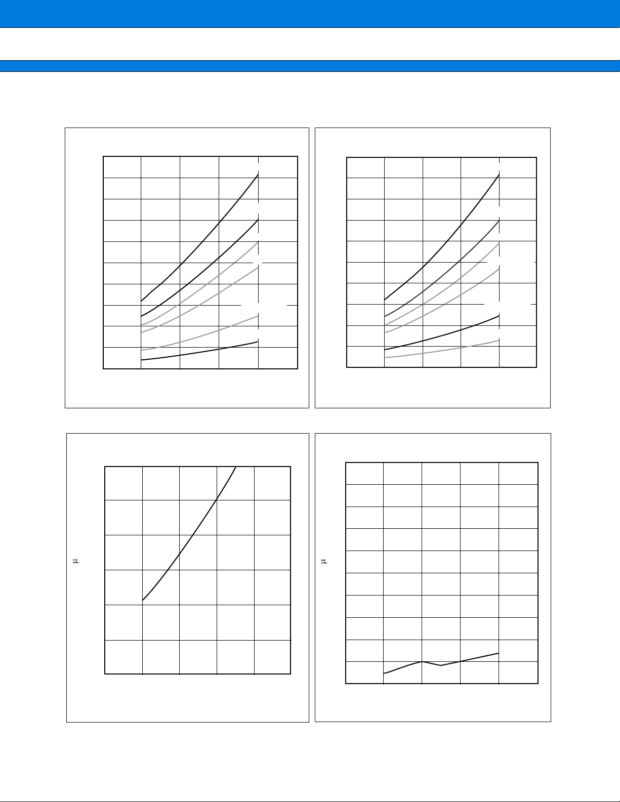
MB90440G Series
• Power Supply Current (FLASH)
50
45
40
35
30
25
Icc [mA]
20
15
10
5
0
2.0 7.06.05.04.03.0
Icc – Vcc
Vcc [V]
(Ta = +25˚C)
fcp = 16 MHz
fcp = 12 MHz
fcp = 10 MHz
fcp = 8 MHz
fcp = 4 MHz
fcp = 2 MHz
20
18
16
14
12
10
Iccs [mA]
8
6
4
2
0
2.0 7.06.05.04.03.0
Iccs – Vcc
(Ta = +25˚C)
fcp = 16 MHz
fcp = 12 MHz
fcp = 10 MHz
fcp = 8 MHz
fcp = 4 MHz
fcp = 2 MHz
Vcc [V]
600
500
400
300
ICTS [ A]
200
100
0
2.0 7.06.05.04.03.0
ICTS – VCC
(fcp = 2 MHz, Ta = +25˚C)
Vcc [V]
ICCH – VCC
(Ta = +25˚C)
20
18
16
14
12
10
ICCT [ A]
8
6
4
2
0
2.0 7.06.05.04.03.0
Vcc [V]
58
Page 59

ORDERING INFORMATION
■
Part number Package Remarks
MB90443GPF (under development)
MB90F443GPF
MB90440G Series
100-pin Plastic QFP
(FPT-100P-M06)
MB90V440GCR
256-pin Ceramic PGA
(PGA-256C-A01)
For evaluation
59
Page 60
MB90440G Series
PACKAGE DIMENSIONS
■
100-pin Plastic QFP
(FPT-100P-M06)
81
INDEX
100
1 30
0.65(.026)
"A"
23.90±0.40(.941±.016)
20.00±0.20(.787±.008)
0.32±0.05
(.013±.002)
Note : Pins width and pins thickness include plating thickness.
5180
50
0.10(.004)
17.90±0.40
(.705±.016)
14.00±0.20
(.551±.008)
Details of "A" part
0.13(.005)
31
M
0.17±0.06
(.007±.002)
3.00
.118
(Mounting height)
0.80±0.20
(.031±.008)
0.88±0.15
(.035±.006)
+0.35
–0.20
+.014
–.008
0.25(.010)
0~8°
0.25±0.20
(.010±.008)
(Stand off)
C
2001 FUJITSU LIMITED F100008S-c-4-4
Dimensions in mm (inches)
60
Page 61

MB90440G Series
FUJITSU LIMITED
All Rights Reserved.
The contents of this document are subject to change without notice.
Customers are advised to consult with FUJITSU sales
representatives before ordering.
The information and circuit diagrams in this document are
presented as examples of semiconductor device applications, and
are not intended to be incorporated in devices for actual use. Also,
FUJITSU is unable to assume responsibility for infringement of
any patent rights or other rights of third parties arising from the use
of this information or circuit diagrams.
The products described in this document are designed, developed
and manufactured as contemplated for general use, including
without limitation, ordinary industrial use, general office use,
personal use, and household use, but are not designed, developed
and manufactured as contemplated (1) for use accompanying fatal
risks or dangers that, unless extremely high safety is secured, could
have a serious effect to the public, and could lead directly to death,
personal injury, severe physical damage or other loss (i.e., nuclear
reaction control in nuclear facility, aircraft flight control, air traffic
control, mass transport control, medical life support system, missile
launch control in weapon system), or (2) for use requiring
extremely high reliability (i.e., submersible repeater and artificial
satellite).
Please note that Fujitsu will not be liable against you and/or any
third party for any claims or damages arising in connection with
above-mentioned uses of the products.
Any semiconductor devices have an inherent chance of failure. You
must protect against injury, damage or loss from such failures by
incorporating safety design measures into your facility and
equipment such as redundancy, fire protection, and prevention of
over-current levels and other abnormal operating conditions.
If any products described in this document represent goods or
technologies subject to certain restrictions on export under the
Foreign Exchange and Foreign Trade Law of Japan, the prior
authorization by Japanese government will be required for export
of those products from Japan.
F0204
FUJITSU LIMITED Printed in Japan
 Loading...