


查询MB90427GCPF供应商
FUJITSU SEMICONDUCTOR
DATA SHEET
DS07-13711-4E
16-Bit Original Microcontroller
CMOS
F2MC-16LX MB90420G/425G Series
MB90423GA/423GC/F423GA/F423GC/427GA/427GC/428GA/428GC/
MB90F428GA/F428GC/V420G
DESCRIPTIONS
■
The FUJITSU MB90420G/425G Series is a 16-bit general purpose high-capacity microcontroller designed for
vehicle meter control applications etc.
The instruction set retains the same A T architecture as the FUJITSU original F
further refinements including high-level language instructions, expanded addressing mode, enhanced (signed)
multipler-divider computation and bit processing.
2
MC-8L and F2MC-16L series, with
In addition, a 32-bit accumulator is built in to enable long word processing.
FEATURES
■
• 16-bit input capture (4 channels)
Detects rising, falling, or both edges.
16-bit capture register × 4
Pin input edge detection latches the 16-bit free-run timer counter value, and generates an interrupt request.
• 16-bit reload timer (2 channels)
16-bit reload timer operation (select toggle output or one-shot output)
Event count function selection provided
PACKAGES
■
Plastic QFP, 100-pin Plastic LQFP, 100-pin
(Continued)
(FPT-100P-M06) (FPT-100P-M05)

MB90420G/425G Series
• Watch timer (main clock)
Operates directly from oscillator clock.
Compensates for oscillator deviation
Read/write enabled second/minute/hour register
Signal interrupt
• 16-bit PPG (3 channels)
Output pins (3) , external trigger input pin (1)
Output clock frequencies : f
CP, fCP/2
2
, fCP/24, fCP/2
• Delay interrupt
Generates interrupt for task switching.
Interruptions to CPU can be generated/deleted by software setting.
• External interrupts (8 channels)
8-channel independent operation
Interrupt source setting available : “L” to “H” edge/ “H” to “L” edge/ “L” level/ “H” level.
• A/D converter
10-bit or 8-bit resolution × 8 channels (input multiplexed)
Conversion time : 6.13 µs or less (at f
CP = 16 MHz)
External trigger startup available (P50/INT0/ADTG)
Internal timer startup available (16-bit reload timer 1)
• UART (2 channels)
Full duplex double buffer type
Supports asynchronous/synchronous transfer (with start/stop bits)
Internal timer can be selected as clock (16-bit reload timer 0)
Asynchronous : 4808 bps, 5208 bps, 9615 bps, 10417 bps, 19230 bps, 38460 bps, 62500 bps, 500000 bps
Synchronous : 500 Kbps, 1Mbps, 2Mbps (at f
• CAN interface *
1
Conforms to CAN specifications version 2.0 Part A and B.
Automatic resend in case of error.
Automatic transfer in response to remote frame.
16 prioritized message buffers for data and messages for data and ID
Multiple message support
Receiving filter has flexible configuration : All bit compare/all bit mask/two partial bit masks
Supports up to 1 Mbps
CAN WAKEUP function (connects RX internally to INT0)
• LCD controller/driver (1 channel)
Segment driver and command driver with direct LCD panel (display) drive capability
• Low voltage/Program Looping detect reset *
Automatic reset when low voltage is detected
Program Looping detection function
• Stepping motor controller (4 channels)
High current output for all channels × 4
Synchronized 8/10-bit PWM for all channels × 2
• Sound generator
8-bit PWM signal mixed with tone frequency from 8-bit reload counter.
PWM frequencies : 62.5 kHz, 31.2 kHz, 15.6 kHz, 7.8 kHz (at f
Tone frequencies : 1/2 PWM frequency, divided by (reload frequency +1)
6
CP = 16 MHz)
2
CP = 16MHz)
(Continued)
2

MB90420G/425G Series
(Continued)
• Input/output ports
Push-pull output and Schmitt trigger input
Programmable in bit units for input/output or peripheral signals.
•Flash memory
Supports automatic programming, Embeded Algorithm
Flag indicates algorithm completion
Minato Electronics flash writer
Boot block configuration
Erasable by blocks
Block protection by external programming voltage
*1 : MB90420G series has 2 channels built-in, MB90425G series has 1 channel built-in
*2 : Built-in to MB90420GA/425GA series only. Not built-in to MB90420GC/425GC series.
Embeded Algorithm is a registered trademark of Advanced Micro Devices Inc.
TM
, write/erase/erase pause/erase resume instructions
3

MB90420G/425G Series
PRODUCT LINEUP
■
••••
MB90420G Series
Part
number
Parameter
Configuration
CPU
Clock
System clock
ROM
RAM
CAN interface
Low voltage/
CPU operation
detection reset
Packages
Emulator
dedicated
power supply*
* : When used with emulation pod MB2145-507, use DIP switch S2 setting. For details see the MB2145-50
Hardware Manual (2.7 “Emulator Dedicated Power Supply Pin”) .
MB90F423GA MB90F423GC MB90423GA MB90423GC MB90V420G
Flash ROM model Mask ROM model Evaluation model
F2MC-16LX CPU
1 system 2 systems 1 system 2 systems 2 systems
On-chip PLL clock multiplier type ( × 1, × 2, × 3, × 4, 1/2 when PLL stopped)
Minimum instruction execution time 62.5 ns (with 4 MHz oscillator × 4)
Flash ROM 128 KB Mask ROM 128 KB External
6 KB 6 KB 6 KB
2 channels
Yes No Yes No No
QFP100, LQFP100 PGA-256
No
••••
MB90425G Series
Part number
MB90F428GA MB90F428GC MB90427GA MB90427GC MB90428GA MB90428GC
Parameter
Configuration Flash ROM model Mask ROM model
CPU
2
F
MC-16LX CPU
Clock 1 system 2 systems 1 system 2 systems 1 system 2 systems
System clock
On-chip PLL clock multiplier type ( × 1, × 2, × 3, × 4, 1/2 when PLL stopped)
Minimum instruction execution time 62.5 ns (with 4 MHz oscillator × 4)
ROM Flash ROM 128 KB Mask ROM 64 KB Mask ROM 128 KB
RAM 6 KB 4 KB 6 KB
CAN interface 1 channel
Low voltage/CPU
operation
Yes No Yes No Yes
No
detection reset
Packages QFP100, LQFP100
Emulator
dedicated
power supply
Note : MB90V420G can be used as evaluation model for MB90420G/425G series.
4

PIN ASSIGNMENTS
■
••••
QFP 100
SEG0
SEG1
SEG2
SEG3
SEG4
SEG5
SEG6
SEG7
V
SS
SEG8
SEG9
SEG10
SEG11
P36/SEG12
P37/SEG13
P40/SEG14
P41/SEG15
P42/SEG16
P43/SEG17
P44/SEG18
V
P45/SEG19
P46/SEG20
P47/SEG21
CC
C
10
11
12
13
14
15
16
17
18
19
20
21
22
23
24
25
MB90420G/425G Series
(TOP VIEW)
P06/PPG0/TOT1
P11/TOT0/WOT
P07/PPG1/TIN1
P12/TIN0/IN3
P13/IN2
P14/IN1
P15/IN0
COM0
COM1
COM2
COM3
100
1
2
3
4
5
6
7
8
9
99
98
97
96
95
94
93
92
P05/SCK1/TRG
P10/PPG2
88
89
90
91
P01/SOT0/INT5
P02/SCK0/INT6
P03/SIN1/INT7
P04/SOT1
84
85
86
87
P00/SIN0/INT4
X1
81
X0
80
V
SS
79
X0A
78
83
V
CC
82
P57/SGA
X1A
76
77
RST
75
P56/SGO/FRCK
74
P55/RX0
73
P54/TX0
72
DV
71
P87/PWM2M3
70
P86/PWM2P3
69
P85/PWM1M3
68
P84/PWM1P3
67
DV
66
P83/PWM2M2
65
P82/PWM2P2
64
P81/PWM1M2
63
P80/PWM1P2
62
DV
61
60
P77/PWM2M1
59
P76/PWM2P1
58
P75/PWM1M1
57
P74/PWM1P1
56
DV
55
P73/PWM2M0
54
P72/PWM2P0
53
P71/PWM1M0
52
P70/PWM1P0
51
DV
SS
CC
SS
CC
SS
29
28
27
26
V1
V0
P91/SEG23
P90/SEG22
30
V2
31
37
36
35
34
33
32
P61/AN1
P60/AN0
AVSSP50/INT0/ADTG
AVRH
AVCCV3
(FPT-100P-M06)
40
39
38
V
P63/AN3
P62/AN2
SS
43
42
41
P66/AN6
P65/AN5
P64/AN4
48
47
46
45
44
MD1
MD0
P52/INT2 (/TX1)
P51/INT1 (/RX1)
P67/AN7
50
49
P53/INT3
MD2
5

MB90420G/425G Series
••••
LQFP 100
(TOP VIEW)
P11/TOT0/WOT
P07/PPG1/TIN1
P12/TIN0/IN3
P10/PPG2
P13/IN2
P14/IN1
P15/IN0
COM0
COM1
COM2
COM3
SEG0
SEG1
SEG2
SEG3
SEG4
SEG5
SEG6
SEG7
V
SS
SEG8
SEG9
SEG10
SEG11
P36/SEG12
P37/SEG13
P40/SEG14
P41/SEG15
P42/SEG16
P43/SEG17
P44/SEG18
V
P45/SEG19
P46/SEG20
P47/SEG21
CC
100
98
99
1
2
3
4
5
6
7
8
9
10
11
12
13
14
15
16
17
18
19
20
21
22
23
24
25
C
97
96
95
94
93
92
91
90
P06/PPG0/TOT1
P05/SCK1/TRG
88
89
P01/SOT0/INT5
P02/SCK0/INT6
P03/SIN1/INT7
P04/SOT1
84
85
86
87
P00/SIN0/INT4
X1
81
X0
80
V
SS
79
X0A
78
83
V
CC
82
P57/SGA
X1A
76
77
RST
75
P56/SGO/FRCK
74
P55/RX0
73
P54/TX0
72
DV
71
P87/PWM2M3
70
P86/PWM2P3
69
P85/PWM1M3
68
P84/PWM1P3
67
DV
66
65
P83/PWM2M2
64
P82/PWM2P2
63
P81/PWM1M2
62
P80/PWM1P2
61
DV
60
P77/PWM2M1
59
P76/PWM2P1
58
P75/PWM1M1
57
P74/PWM1P1
56
DV
55
P73/PWM2M0
54
P72/PWM2P0
53
P71/PWM1M0
52
P70/PWM1P0
51
DV
SS
CC
SS
CC
SS
50
49
48
47
46
45
44
43
42
41
40
39
38
37
36
35
34
33
32
31
30
29
28
27
26
P53/INT3
MD2
MD1
MD0
P52/INT2 (/TX1)
P51/INT1 (/RX1)
P67/AN7
P66/AN6
P65/AN5
P64/AN4
V
P63/AN3
P62/AN2
P61/AN1
P60/AN0
AVSSP50/INT0/ADTG
AVRH
AVCCV3
V2
V1
V0
P91/SEG23
P90/SEG22
SS
(FPT-100P-M05)
6

PIN DESCRIPTIONS
■
MB90420G/425G Series
Pin no.
LQFP QFP
80 82 X0
81 83 X1 High speed oscillator output pin.
78 80 X0A
77 79 X1A
75 77 RST
83 85
84 86
85 87
Symbol
P00
SIN0 UART ch.0 serial data input pin.
INT4 INT4 external interrupt input pin.
P01
SOT0 UART ch.0 serial data output pin.
INT5 INT5 external interrupt input pin.
P02
SCK0 UART ch.0 serial clock input/output pin.
INT6 INT6 external interrupt input pin.
Circuit
type
High speed oscillator input pin.
A
Low speed oscillator input pin. If no oscillator is connected, apply
pull-down processing.
A
Low speed oscillator output pin. If no oscillator is connected, leave
open.
B Reset input pin.
General purpose input/output port.
G
General purpose input/output port.
G
General purpose input/output port.
G
Description
86 88
87 89
88 90
89 91
90 92
91 93
P03
SIN1 UART ch.1 serial data input pin.
INT7 INT7 external interrupt input pin.
P04
SOT1 UART ch.1 serial data output pin.
P05
SCK1 UART ch.1 serial clock input/output pin.
TRG 16-bit PPG ch.0-2 external trigger input pin.
P06
PPG0 16-bit PPG ch.0 output pin.
TOT1 16-bit reload timer ch.1 TOT output pin.
P07
PPG1 16-bit PPG ch.1 output pin.
TIN1 16-bit reload timer ch.1 TIN output pin.
P10
PPG2 16-bit PPG ch.2 output pin.
General purpose input/output port.
G
General purpose input/output port.
G
General purpose input/output port.
G
General purpose input/output port.
G
General purpose input/output port.
G
General purpose input/output port.
G
(Continued)
7

MB90420G/425G Series
Pin no.
LQFP QFP
92 94
93 95
94 to 96 96 to 98
97 to 100
1 to 8,
10 to 13
14 to 15 16 to 17
16 to 20,
22 to 24
99 to 100,
1 to 2
3 to 10,
12 to 15
18 to 22,
24 to 26
Symbol
P11
TOT0 16-bit reload timer ch.0 TOT output pin.
WOT Real-time watch timer WOT output pin.
P12
TIN0 16-bit reload timer ch.0 TIN output pin.
IN3 Input capture ch.3 trigger input pin.
P13 to P15
IN2 to IN0 Input capture ch.0-2 trigger input pins.
COM0 to
COM3
SEG0 to
SEG11
P36 to P37
SEG12 to
SEG13
P40 to P47
SEG14 to
SEG21
Circuit
type
General purpose input/output port.
G
General purpose input/output port.
G
General purpose input/output ports.
G
I LCD controller/driver common output pins.
I LCD controller/driver segment output pins.
General purpose output ports.
E
LCD controller/driver segment output pins.
General purpose input output ports.
E
LCD controller/driver segment output pins.
Description
26 to 27 28 to 29
34 36
36 to 39,
41 to 44
45 47
46 48
50 52
38 to 41,
43 to 46
P90 to P91
SEG22 to
SEG23
P50
INT0 INT0 external interrupt input pin.
ADTG A/D converter external trigger input pin.
P60 to P67
AN0 to
AN7
P51
INT1 INT1 external interrupt input pin.
(RX1 *
(TX1 *
1
) CAN interface 1 RX intput pin.
P52
INT2 INT2 external interrupt input pin.
1
) CAN interface 1 TX output pin.
P53
INT3 INT3 external interrupt input pin.
General purpose input output ports.
E
LCD controller/driver segment output pins.
General purpose input output ports.
G
General purpose input output ports.
F
A/D converter input pins.
General purpose input output port.
G
General purpose input output port.
G
General purpose input output port.
G
(Continued)
8

MB90420G/425G Series
Pin no.
LQFP QFP
52 to 55 54 to 57
57 to 60 59 to 62
62 to 65 64 to 67
67 to 70 69 to 72
Symbol
P70 to P73
PWM1P0
PWM1M0
PWM2P0
PWM2M0
P74 to P77
PWM1P1
PWM1M1
PWM2P1
PWM2M1
P80 to P83
PWM1P2
PWM1M2
PWM2P2
PWM2M2
P84 to P87
PWM1P3
PWM1M3
PWM2P3
PWM2M3
Circuit
type
H
H
H
H
Description
General purpose input output ports.
Stepping motor controller ch.0 output pins.
General purpose input output ports.
Stepping motor controller ch.1 output pins.
General purpose input output ports.
Stepping motor controller ch.2 output pins.
General purpose input output ports.
Stepping motor controller ch.3 output pins.
72 74
P54
General purpose input output port.
G
TX0 CAN interface 0 TX output pin.
73 75
P55
General purpose output port.
G
RX0 CAN interface 0 RX input pin.
74 76
P56
SGO Sound generator SG0 output pin.
General purpose input output port.
G
FRCK Free-run timer clock input pin.
76 78
P57
General purpose input output port.
G
SGA Sound generator SGA output pin.
28 to 31 30 to 33 V0 to V3 LCD controller /driver reference power supply pins.
56, 66 58, 68 DV
51, 61, 71 53, 63, 73 DV
CC
SS
High current output buffer with dedicated power supply input pins
(pin numbers 54-57, 59-62, 64-67, 69-72) .
High current output buffer with dedicated power supply GND pins
(pin numbers 54-57, 59-62, 64-67, 69-72) .
32 34 AVCC A/D converter dedicated power supply input pin.
35 37 AV
SS A/D converter dedicated GND supply pin.
33 35 AVRH A/D converter Vref + input pin. Vref − AVss.
(Continued)
9

MB90420G/425G Series
(Continued)
Pin no.
Symbol
LQFP QFP
47
48
49
50
MD0
MD1
49 51 MD2 C/D *
Circuit
type
C Test mode input pins. Connect to V
2
Text mode input pin. Connect to VSS.
Description
CC.
25 27 C
21, 82 23, 84 V
CC Power supply input pins.
External capacitor pin. Connect an 0.1 µF capacitor between this
pin and V
SS.
9, 40, 79 11, 42, 81 VSS GND power supply pins.
*1 : MB90420G series only.
*2 : Type C in the flash ROM models, type D in the mask ROM models.
10

MB90420G/425G Series
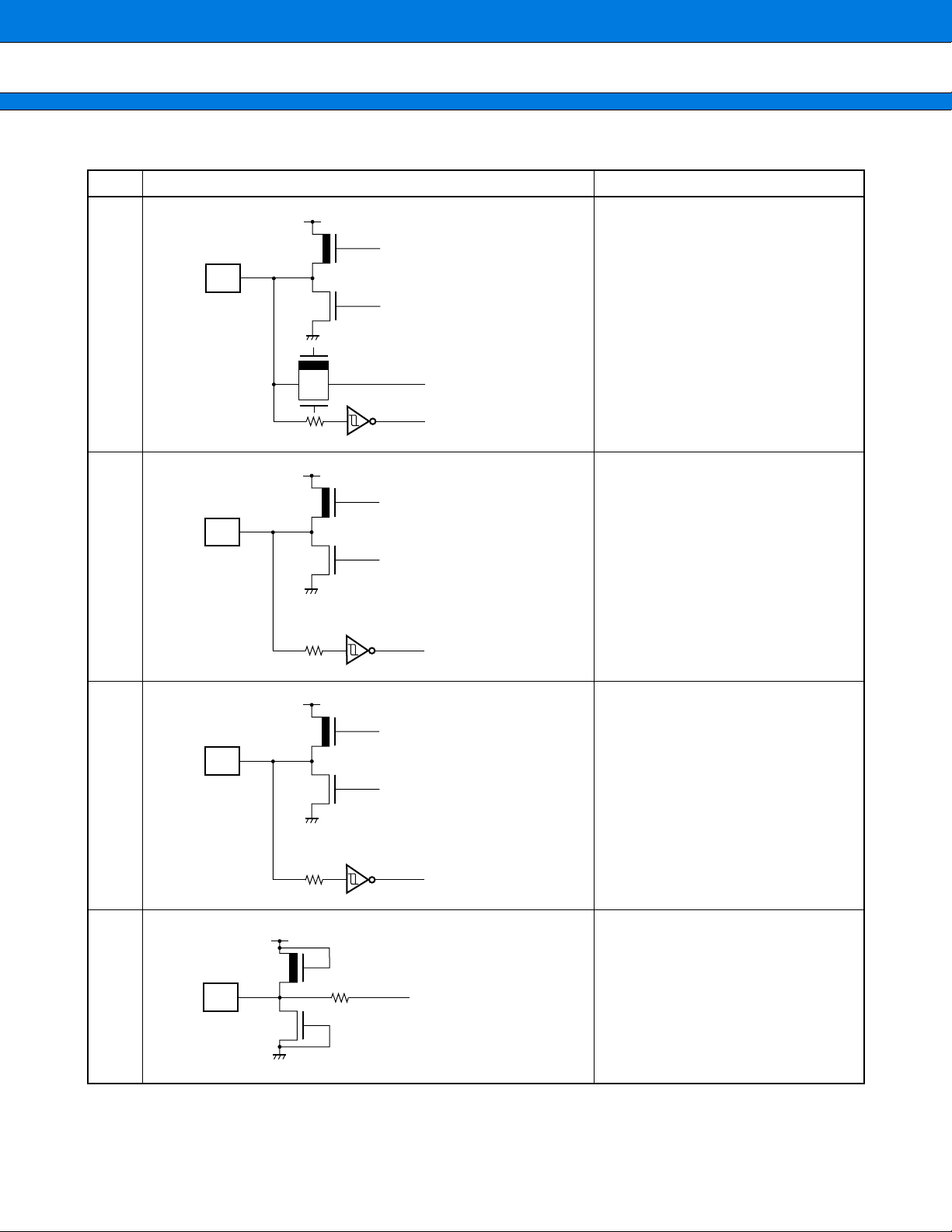
I/O CIRCUIT TYPE
■
Type Circuit Remarks
X1/X1A
• Oscillation feedback resistance :
approx. 1 MΩ (X0, X1 : MAIN)
• Oscillation feedback resistance :
approx. 10 MΩ (X0A, X1A : SUB)
A
X0/X0A
Standby control signal
• Pull-up resistance attached :
approx. 50 kΩ, hysteresis input
B
Hysteresis input
• Hysteresis input
C
Hysteresis input
• Pull-down resistance attached :
approx. 50 kΩ, hysteresis input
Hyteresis input
D
• CMOS output
• LCDC output
• Hysteresis input
E
LCDC output
Hysteresis input
(Continued)
11
MB90420G/425G Series
(Continued)
Type Circuit Remarks
• CMOS output
• Hysteresis input
• Analog input
F
Analog input
Hysteresis input
• CMOS output
• Hysteresis input
G
Hysteresis input
• CMOS high current output
• Hysteresis input
High current
H
Hysteresis input
• LCDC output
I
LCDC output
12

HANDLING DEVICES
■
Precautions for Handling Semiconductor Devices
• Strictly observe maximum rated voltages (prevent latchup)
MB90420G/425G Series
When CMOS integrated circuit devices are subjected to applied voltages higher than V
pins other than medium- and high-withstand voltage pins, or to voltages lower than V
excess of rated le vels are applied between V
CC and VSS, a phenomenon known as latchup can occur . In a latchup
CC at input and output
SS, or when voltages in
condition, supply current can increase dramatically and may destroy semiconductor elements. In using semiconductor devices, always take sufficient care to avoid exceeding maximum ratings.
Also care must be taken when power to analog systems is switched on or off, to ensure that the analog power
supply (AV
do not exceed the digital power supply (V
CC, AVRH) , analog input and dedicated power supply for the high current output buffer pins (DVCC)
CC) .
Once the digital power supply (VCC) is switched on, the analog po wer (AVCC,AVRH) and dedicated power supply
for the high current output buffer pins (DV
CC) may be turned on in any sequence.
• Stable supply voltage
Even within the warranted operating range of V
CC supply voltage, sudden fluctuations in supply voltage can
cause abnormal operation. The recommended stability for ripple fluctuations (P-P values) at commercial frequencies (50 Hz to 60 Hz) should be within 10% of the standard V
CC value, and voltage fluctuations that occur
during switching of power supplies etc. should be limited to transient fluctuation rates of 0.1 V/ms or less.
• Power-on procedures
In order to prevent abnormal operation of the internal built-in step-down circuits, v oltage rise time during poweron should be attained within 50 µs (0.2 V to 2.7 V) .
• Treatment of unused pins
If unused input pins are left open, they ma y cause abnormal operation or latchup which may lead to permanent
damage to the semiconductor. An y such pins should be pulled up or pulled do wn through resistance of at least
2 kΩ.
Any unused input/output pins should be left open in output status, or if found set to input status , they should be
treated in the same way as input pins.
Any unused output pins should be left open.
• Treatment of A/D converter power supply pins
Even if the A/D converter is not used, pins should be connected so that AV
CC = VCC, and AVSS = AVRH = VSS.
• Use of external clock signals
Even when an external clock is used, a stabilization period is required following a power-on reset or release
from sub clock mode or stop mode. Also, when an e xternal clock is used it should drive only the X0 pin and the
X1 pin should be left open, as shown in Figure 3.
X0
OPEN
X1
MB90420G/425G Series
Sample external clock connection
13

MB90420G/425G Series
• Power supply pins
Devices are designed to pre vent problems such as latchup when multiple V
CC and VSS supply pins are used, by
providing internal connections between pins having the same potential. However, in order to reduce unwanted
radiation, and to prevent abnormal operation of strobe signals due to rise in ground level, and to maintain total
output current ratings, all such pins should always be connected externally to power supplies and ground.
As shown in figure below, all V
should be handled in the same way. If there are multiple V
CC power supply pins must have the same potential. All VSS power supply pins
CC or VSS systems, the device will not operate properly
even within the warranted operating range.
VCC
VSS
VCC
VSS
VCC
VSS
VSS
VCC
VSS
VCC
Power supply input pins (VCC/VSS)
In addition, care must be given to connecting the V
impedance as possible. It is recommended that a bypass capacitor of 1.0 µF be connected between V
V
SS as close to the pins as possible.
CC and VSS pins of this device to a current source with as little
CC and
• Proper sequence of A/D converter power supply analog input
A/D converter power (AV
(V
CC) is switched on. When power is shut off, the A/D converter power supply and analog input must be cut off
before the digital power supply is switched on (V
AVRH does not exceed AV
sure that the input voltage does not exceed AV
CC, AVRH) and analog input (AN0-AN7) must be applied after the digital power supply
CC) . In both power-on and shut-off, care should be taken that
CC. Even when pins which double as analog input pins are used as input por ts, be
CC. (There is no problem if analog power supplies and digital
power supplies are turned off and on at the same time.)
CC
• Handling the power supply for high-current output buffer pins (DV
Always apply pow er to high-current output b uffer pins (DV
CC, D VSS) after the digital po w er supply (VCC) is turned
on. Also when switching power off, alw a ys shut off the power supply to the high-current output b uffer pins (DV
DV
SS) before s witching off the digital po w er supply (VCC) . (There will be no problem if high-current output buffer
, DVSS)
CC,
pins and digital power supplies are turned off and on at the same time.)
Even when high-current output buff er pins are used as gener al purpose ports, the power for high current output
buffer pins (DV
CC, DVSS) should be applied to these pins.
• Pull-up/pull-down resistance
The MB90420G/425G series does not support internal pull-up/pull-down resistance. If necessary, use external
components.
14

MB90420G/425G Series
• Precautions for when not using a sub clock signal.
If the X0A and X1A pins are not connected to an oscillator, apply pull-down treatment to the X0A pin and leav e
the X1A pin open.
• Notes on during operation of PLL clock mode
If the PLL clock mode is selected, the microcontroller attempt to be working with the self-oscillating circuit ev en
when there is no external oscillator or external clock input is stopped. Performance of this operation, however,
cannot be guaranteed.
15

MB90420G/425G Series
BLOCK DIAGRAM
■
X0, X1
X0A, X1A
RST
P57/SGA
P56/SGO/FRCK
P55/RX0
P54/TX0
P53/INT3
P52/INT2 (/TX1)
P51/INT1 (/RX1)
P50/INT0/ADTG
P00/SIN0/INT4
P01/SOT0/INT5
P02/SCK0/INT6
P03/SIN1/INT7
P04/SOT1
P05/SCK1/TRG
P06/PPG0/TOT1
P07/PPG1/TIN1
P10/PPG2
P11/TOT0/WOT
P12/TIN0/IN3
P13/IN2
P14/IN1
P15/IN0
Clock control
circuit
RAM
ROM
Sound generator
CAN controller
Port 5
External interrupt
(8 ch)
UART0/1
Prescaler
Port 0
PPG0/1/2
Port 1
Reload timer
Real-time
Watch timer
ICU0/1/2/3
0/1
0/1
CPU
F2MC-16LX core
MC-16LX BUS
2
F
Interrupt
controller
Low voltage/
CPU operation
detection reset
Port 8
Stepping
motor
Controller
0/1/2/3
Port 7
Port 6
A/D converter
(8 ch)
Port 9
Port 4
Port 3
P87/PWM2M3
P86/PWM2P3
P85/PWM1M3
P84/PWM1P3
P83/PWM2M2
P82/PWM2P2
P81/PWM1M2
P80/PWM1P2
P77/PWM2M1
P76/PWM2P1
P75/PWM1M1
P74/PWM1P1
P73/PWM2M0
P72/PWM2P0
P71/PWM1M0
P70/PWM1P0
P67 to P60/
AN7 to AN0
AV
CC/AVSS
AVRH
P91, P90/
SEG23, SEG22
P47 to P40/
SEG21 to SEG14
P37, P36/
SEG13 to SEG12
Free-run timer
Evaluation device (MB90V420G)
No built-in ROM
Built-in RAM is 6 KB.
LCD controller/
driver
SEG11 to SEG0
COM3 to COM0
V3 to V0
Note: MB90420G series is equipped with 2-channel CAN interface and MB90425G series is equipped with 1-channel
CAN interface. MB90F423GA, MB90423GA, MB90F428GA, MB90427GA and MB90428GA have low voltage/CPU operation detection reset. MB90F423GC, MB90423GC , MB90F428GC, MB90427GC, MB90428GC
and MB90V420G do not have low voltage/CPU operation detection reset.
See “■ Product Lineup” for detail.
16

■■■■ MEMORY MAP
000000H
0000C0H
MB90420G/425G Series
Single chip mode
(with ROM mirror function)
Peripheral area
000100H
Address #2
003900
004000H
010000H
Address #1
FFFFFFH
Register
RAM area
H
Peripheral area
ROM area
(FF bank image)
ROM area
: Internal access memory
: Access prohibited
Parts No. Address #1 Address #2
MB90423GA/GC FE0000
H 001900H
MB90427GA/GC FF0000H 001100H
MB90428GA/GC FE0000H 001900H
MB90F423GA/GC FE0000H 001900H
MB90F428GA/GC FE0000H 001900H
MB90V420G FE0000H 001900H
Note : To select models without the ROM mirror function, see the “ROM Mirror Function Selection Module.” The
image of the ROM data in the FF bank appears at the top of the 00 bank, in order to enable efficient use of
small C compiler models. The lower 16-bit address for the FF bank will be assigned to the same address,
so that tables in ROM can be referenced without declaring a “far” indication with the pointer. For example
when accessing the address 00C000
H, the actual access is to address FFC000H in ROM. Here the FF bank
ROM area exceeds 48 KB, so that it is not possible to see the entire area in the 00 bank image. Therefore
because the ROM data from FF4000
recommended that the ROM data table be stored in the area from FF4000
H to FFFFFFH will appear in the image from 004000H to 00FFFFH, it is
H to FFFFFFH.
17

MB90420G/425G Series
I/O MAP
■
• Other than CAN Interface
Address Register name Symbol Read/write Peripheral function Initial value
00
H Port 0 data register PDR0 R/W Port 0 XXXXXXXX
01
H Port 1 data register PDR1 R/W Port 1 - - XXXXXX
02H (Disabled)
03
H Port 3 data register PDR3 R/W Port 3 XX - - - - - -
04
H Port 4 data register PDR4 R/W Port 4 XXXXXXXX
05H Port 5 data register PDR5 R/W Port 5 XXXXXXXX
06
H Port 6 data register PDR6 R/W Port 6 XXXXXXXX
07
H Port 7 data register PDR7 R/W Port 7 XXXXXXXX
08H Port 8 data register PDR8 R/W Port 8 XXXXXXXX
09
H Port 9 data register PDR9 R/W Port 9 - - - - - -XX
0A
H to
0F
H
10H Port 0 direction register DDR0 R/W Port 0 0 0 0 0 0 0 0 0
(Disabled)
11
H Port 1 direction register DDR1 R/W Port 1 - - 0 0 0 0 0 0
12
H (Disabled)
13H Port 3 direction register DDR3 R/W Port 3 0 0 - - - - - -
14
H Port 4 direction register DDR4 R/W Port 4 0 0 0 0 0 0 0 0
15
H Port 5 direction register DDR5 R/W Port 5 0 0 0 0 0 0 0 0
16
H Port 6 direction register DDR6 R/W Port 6 0 0 0 0 0 0 0 0
17H Port 7 direction register DDR7 R/W Port 7 0 0 0 0 0 0 0 0
18
H Port 8 direction register DDR8 R/W Port 8 0 0 0 0 0 0 0 0
19
H Port 9 direction register DDR9 R/W Port 9 - - - - - - 0 0
1AH Analog input enable ADER R/W Port 6, A/D 1 1 1 1 1 1 1 1
1B
H to
1F
H
20
H A/D control status register lower ADCSL R/W
(Disabled)
0 0 0 0 0 0 0 0
21H A/D control status register higher ADCSH R/W 0 0 0 0 0 0 0 0
A/D converter
22
H A/D data register lower ADCRL R XXXXXXXX
23
H A/D data register higher ADCRH R/W 0 0 1 0 1 XXX
24H
R/W
XXXXXXXX
Compare clear register CPCLR
25
H R/W XXXXXXXX
18
26
H
Timer data register TCDT
H R/W 0 0 0 0 0 0 0 0
27
R/W 0 0 0 0 0 0 0 0
16-bit free-run timer
28H Timer control status register lower TCCSL R/W 0 0 0 0 0 0 0 0
29
H Timer control status register higher TCCSH R/W 0 - - 0 0 0 0 0
(Continued)

MB90420G/425G Series
Address Register name Symbol Read/write Peripheral function Initial value
2A
H PPG0 control status register lower PCNTL0 R/W
16-bit PPG0
2BH PPG0 control status register higher PCNTH0 R/W 0 0 0 0 0 0 0 -
2C
H PPG1 control status register lower PCNTL1 R/W
16-bit PPG1
2D
H PPG1 control status register higher PCNTH1 R/W 0 0 0 0 0 0 0 -
2E
H PPG2 control status register lower PCNTL2 R/W
16-bit PPG2
2FH PPG2 control status register higher PCNTH2 R/W 0 0 0 0 0 0 0 -
30
H External interrupt enable ENIR R/W
31
H External interrupt request EIRR R/W 0 0 0 0 0 0 0 0
External interrupt
32H External interrupt level lower ELVRL R/W 0 0 0 0 0 0 0 0
33
H External interrupt level higher ELVRH R/W 0 0 0 0 0 0 0 0
34
H Serial mode register 0 SMR0 R/W
35H Serial control register 0 SCR0 R/W 0 0 0 0 0 1 0 0
36
Input data register 0/
H
Output data register 0
SIDR0/
SODR0
R/W XXXXXXXX
UART 0
0 0 0 0 0 0 0 0
0 0 0 0 0 0 0 0
0 0 0 0 0 0 0 0
0 0 0 0 0 0 0 0
0 0 0 0 0 - 0 0
37
H Serial status register 0 SSR0 R/W 0 0 0 0 1 0 0 0
38H Serial mode register 1 SMR1 R/W
39
H Serial control register 1 SCR1 R/W 0 0 0 0 0 1 0 0
3A
3B
Input data register 1/
H
Output data register 1
H Serial status register 1 SSR1 R/W 0 0 0 0 1 0 0 0
SIDR1/
SODR1
R/W XXXXXXXX
UART1
0 0 0 0 0 − 0 0
3CH (Disabled)
3D
H Clock division control register 0 CDCR0 R/W Prescaler 0 - - - 0 0 0 0
3E
H CAN wake-up control register CWUCR R/W CAN - - - - - - - 0
3FH Clock division control register 1 CDCR1 R/W Prescaler 0 - - - 0 0 0 0
40
H to 4FH Area reserved for CAN interface 0
50
H Timer control status register 0 lower TMCSR0L R/W
51H
52
53
Timer control status register 0 higher
H
Timer register 0/
Reload register 0
H XXXXXXXX
TMCSR0H R/W - - - 0 0 0 0 0
16-bit reload timer 0
TMR0/
TMRLR0
R/W
54H Timer control status register 1 lower TMCSR1L R/W
55
56
57
58H Watch timer control register lower WTCRL R/W
59
Timer control status register 1 high-
H
er
H
Timer register 1/
Reload register 1
H XXXXXXXX
TMCSR1H R/W - - - 0 0 0 0 0
16-bit reload timer 1
TMR1/
TMRLR1
R/W
Real-time
H Watch timer control register higher WTCRH R/W 0 0 0 0 0 0 0 0
watch timer
0 0 0 0 0 0 0 0
XXXXXXXX
0 0 0 0 0 0 0 0
XXXXXXXX
0 0 0 - - 0 0 0
(Continued)
19

MB90420G/425G Series
Address Register name Symbol Read/write Peripheral function Initial value
5A
H Sound control register lower SGCRL R/W
5BH Sound control register higher SGCRH R/W 0 - - - - - 0 0
5C
H Frequency data register SGFR R/W XXXXXXXX
Sound generator
5D
H Amplitude data register SGAR R/W 0 0 0 0 0 0 0 0
5E
H Decrement grade register SGDR R/W XXXXXXXX
5FH Tone count register SGTR R/W XXXXXXXX
0 0 0 0 0 0 0 0
60
H
XXXXXXXX
Input capture register 0 IPCP0 R
61
H XXXXXXXX
Input capture 0/1
62H
XXXXXXXX
Input capture register 1 IPCP1 R
63
H XXXXXXXX
64
H
XXXXXXXX
Input capture register 2 IPCP2 R
65
H XXXXXXXX
Input capture 2/3
66
H
XXXXXXXX
Input capture register 3 IPCP3 R
H XXXXXXXX
67
68H Input capture control status 0/1 ICS01 R/W Input capture 0/1 0 0 0 0 0 0 0 0
69
H (Disabled)
6A
H Input capture control status 2/3 ICS23 R/W Input capture 2/3 0 0 0 0 0 0 0 0
6B
H (Disabled)
6CH LCD control register lower LCRL R/W
6D
H LCD control register higher LCRH R/W 0 0 0 0 0 0 0 0
6E
Low voltage/CPU operation
H
detection reset control register
LVRC R/W
LCD controller/
driver
Low voltage/CPU opera-
tion detection reset
0 0 0 1 0 0 0 0
1 0 1 1 1 0 0 0
6FH ROM mirror ROMM W ROM mirror XXXXXXX1
70
H to 7FH Area reserved for CAN interface 1
20
80
H PWM control register 0 PWC0 R/W
Stepping motor
controller0
0 0 0 0 0 - - 0
81H (Disabled)
82
H PWM control register 1 PWC1 R/W
83
H (Disabled)
Stepping motor
controller1
0 0 0 0 0 - - 0
84H PWM control register 2 PWC2 R/W Stepping motor controller2 0 0 0 0 0 - - 0
85
H (Disabled)
86
H PWM control register 3 PWC3 R/W Stepping motor controller3 0 0 0 0 0 - - 0
87
9D
H to
H
(Disabled)
(Continued)

MB90420G/425G Series
Address Register name Symbol Read/write Peripheral function Initial value
9E
H ROM correction control register PACSR R/W
9F
H Delay interrupt/release DIRR R/W Delayed interrupt - - - - - - - 0
A0H Power saving mode LPMCR R/W
A1
H Clock select CKSCR R/W 1 1 1 1 1 1 0 0
A2
A7
H to
H
(Disabled)
Address match
detection function
Power saving
control circuit
- - - - - 0 - 0
0 0 0 1 1 0 0 0
A8H Watchdog control WDTC R/W Watchdog timer XXXXX 1 1 1
A9
H Time base timer control register TBTC R/W Time base timer 1 - - 0 0 1 0 0
AA
H Watch timer control register WTC R/W
ABH to
AD
H
AE
H Flash control register FMCS R/W Flash interface 0 0 0 X 0 XX 0
AF
H (Disabled)
(Disabled)
B0H Interrupt control register 00 ICR00 R/W
B1
H Interrupt control register 01 ICR01 R/W 0 0 0 0 0 1 1 1
B2
H Interrupt control register 02 ICR02 R/W 0 0 0 0 0 1 1 1
B3
H Interrupt control register 03 ICR03 R/W 0 0 0 0 0 1 1 1
Watch timer
(sub-clock)
1 X 0 0 0 0 0 0
0 0 0 0 0 1 1 1
B4H Interrupt control register 04 ICR04 R/W 0 0 0 0 0 1 1 1
B5
H Interrupt control register 05 ICR05 R/W 0 0 0 0 0 1 1 1
B6
H Interrupt control register 06 ICR06 R/W 0 0 0 0 0 1 1 1
B7H Interrupt control register 07 ICR07 R/W 0 0 0 0 0 1 1 1
Interrupt controller
B8
H Interrupt control register 08 ICR08 R/W 0 0 0 0 0 1 1 1
B9
H Interrupt control register 09 ICR09 R/W 0 0 0 0 0 1 1 1
BAH Interrupt control register 10 ICR10 R/W 0 0 0 0 0 1 1 1
BB
H Interrupt control register 11 ICR11 R/W 0 0 0 0 0 1 1 1
BC
H Interrupt control register 12 ICR12 R/W 0 0 0 0 0 1 1 1
BDH Interrupt control register 13 ICR13 R/W 0 0 0 0 0 1 1 1
BE
H Interrupt control register 14 ICR14 R/W 0 0 0 0 0 1 1 1
BF
H Interrupt control register 15 ICR15 R/W 0 0 0 0 0 1 1 1
C0H to
FF
H
(Disabled)
(Continued)
21

MB90420G/425G Series
Address Register name Symbol Read/write Peripheral function Initial value
1FF0
H ROM correction address 0 PADR0 R/W
1FF1H ROM correction address 1 PADR0 R/W XXXXXXXX
1FF2
H ROM correction address 2 PADR0 R/W XXXXXXXX
1FF3
H ROM correction address 3 PADR1 R/W XXXXXXXX
1FF4
H ROM correction address 4 PADR1 R/W XXXXXXXX
Address match
detection function
1FF5H ROM correction address 5 PADR1 R/W XXXXXXXX
3900
391F
H to
H
(Disabled)
XXXXXXXX
3920
H
PPG0 down counter register PDCR0 R
3921
H 1 1 1 1 1 1 1 1
3922
H
PPG0 cycle setting register PCSR0 W
H XXXXXXXX
3923
16-bit PPG 0
3924H
PPG0 duty setting register PDUT0 W
3925
H XXXXXXXX
3926
3927
H to
H
(Disabled)
3928H
PPG1 down counter register PDCR1 R
3929
H 1 1 1 1 1 1 1 1
392A
H
PPG1 cycle setting register PCSR1 W
H XXXXXXXX
392B
16-bit PPG 1
392CH
PPG1 duty setting register PDUT1 W
392D
H XXXXXXXX
392E
392F
H to
H
(Disabled)
3930H
PPG2 down counter register PDCR2 R
3931
H 1 1 1 1 1 1 1 1
1 1 1 1 1 1 1 1
XXXXXXXX
XXXXXXXX
1 1 1 1 1 1 1 1
XXXXXXXX
XXXXXXXX
1 1 1 1 1 1 1 1
22
3932
H
PPG2 cycle setting register PCSR2 W
H XXXXXXXX
3933
3934
H
16 bit PPG 2
PPG2 duty setting register PDUT2 W
3935
H XXXXXXXX
3936H to
3959
H
(Disabled)
XXXXXXXX
XXXXXXXX
(Continued)

MB90420G/425G Series
Address Register name Symbol Read/write Peripheral function Initial value
395A
H
395B
395C
395D
395E
Sub second data register WTBR R/W
H XXXXXXXX
H - - - XXXXX
H Second data register WTSR R/W - - XXXXXX
H Minute data register WTMR R/W - - XXXXXX
Real time
watch timer
XXXXXXXX
395FH Hour data register WTHR R/W - - - XXXXX
3960
396B
396C
397F
3980H
H to
LCD display RAM VRAM R/W
H
H to
H
(Disabled)
LCD controller/
driver
XXXXXXXX
XXXXXXXX
PWM1 compare register 0 PWC10 R/W
3981
H - - - - - - XX
3982
H
PWM2 compare register 0 PWC20 R/W
H - - - - - - XX
3983
3984
H PWM1 select register 0 PWS10 R/W - - 0 0 0 0 0 0
3985
H PWM2 select register 0 PWS20 R/W - 0 0 0 0 0 0 0
3986H to
3987
H
(Disabled)
Stepping motor
controller 0
XXXXXXXX
3988
H
XXXXXXXX
PWM1 compare register 1 PWC11 R/W
3989
H - - - - - - XX
398A
H
PWM2 compare register 1 PWC21 R/W
H - - - - - - XX
398B
398C
H PWM1 select register 1 PWS11 R/W - - 0 0 0 0 0 0
398D
H PWM2 select register 1 PWS21 R/W - 0 0 0 0 0 0 0
398EH to
398F
H
3990
H
(Disabled)
Stepping motor
controller 1
XXXXXXXX
XXXXXXXX
PWM1 compare register 2 PWC12 R/W
3991
H - - - - - - XX
3992H
PWM2 compare register 2 PWC22 R/W
3993
H - - - - - - XX
3994
H PWM1 select register 2 PWS12 R/W - - 0 0 0 0 0 0
Stepping motor
controller 2
XXXXXXXX
3995H PWM2 select register 2 PWS22 R/W - 0 0 0 0 0 0 0
3996
3997
H to
H
(Disabled)
(Continued)
23

MB90420G/425G Series
(Continued)
Address Register name Symbol Read/write Peripheral function Initial value
3998
H
XXXXXXXX
PWM1 compare register 3 PWC13 R/W
3999
H - - - - - - XX
399A
H
PWM2 compare register 3 PWC23 R/W
399B
H - - - - - - XX
399C
H PWM1 select register 3 PWS13 R/W - - 0 0 0 0 0 0
Stepping motor
controller 3
XXXXXXXX
399DH PWM2 select register 3 PWS23 R/W - 0 0 0 0 0 0 0
399E
H to
39FF
H
3A00
H to
3AFF
H
3B00H to
3BFF
H
3C00
H to
3CFF
H
3D00
H to
3DFF
H
3E00H to
3EFF
H
Area reserved for CAN interface 0
Area reserved for CAN interface 1
Area reserved for CAN interface 0
Area reserved for CAN interface 1
(Disabled)
(Disabled)
• Initial value symbols :
“0” initial value 0.
“1” initial value 1.
“X” initial value undetermined
“-” initial value undetermined (none)
• Write/read symbols :
“R/W” read/write enabled
“R” read only
“W” write only
• Addresses in the area 0000
H to 00FFH are reserved for the principal functions of the MCU. Read access
attempts to reserved areas will result in an “X” value. Also, wr ite access to reserved areas is prohibited.
24

• I/O Map for CAN Interface
Address
CAN0 CAN1
000040
H 000070H
Message buffer valid area BVALR (R/W) 0 0 0 0 0 0 0 0 0 0 0 0 0 0 0 0
000041
H 000071H
MB90420G/425G Series
Register name Symbol
Read/
write
Initial value
000042H 000072H
000043
H 000073H
000044H 000074H
000045
H 000075H
000046H 000076H
000047
H 000077H
000048H 000078H
000049
H 000079H
00004AH 00007AH
00004B
H 00007BH
00004CH 00007CH
00004D
H 00007DH
00004EH 00007EH
00004F
H 00007FH
003C00H 003D00H
003C01
H 003D01H
003C02H 003D02H
003C03
H 003D03H
003C04H 003D04H
003C05
H 003D05H
Transmission request register TREQR (R/W) 0 0 0 0 0 0 0 0 0 0 0 0 0 0 0 0
Transmission cancel register TCANR (W) 0 0 0 0 0 0 0 0 0 0 0 0 0 0 0 0
Transmission completed register TCR (R/W) 0 0 0 0 0 0 0 0 0 0 0 0 0 0 0 0
Receiving completed register RCR (R/W) 0 0 0 0 0 0 0 0 0 0 0 0 0 0 0 0
Remote request receiving register RRTRR (R/W) 0 0 0 0 0 0 0 0 0 0 0 0 0 0 0 0
Receiving overrun register ROVRR (R/W) 0 0 0 0 0 0 0 0 0 0 0 0 0 0 0 0
Receiving interrupt enable register RIER (R/W) 0 0 0 0 0 0 0 0 0 0 0 0 0 0 0 0
Control status register CSR (R/W, R) 0 0 - - - 0 0 0 0 - - - - 0 - 1
Last event indicator register LEIR (R/W) - - - - - - - - 0 0 0 - 0 0 0 0
RX/TX error counter RTEC (R) 0 0 0 0 0 0 0 0 0 0 0 0 0 0 0 0
003C06H 003D06H
003C07
H 003D07H
003C08H 003D08H
003C09
H 003D09H
003C0AH 003D0AH
003C0B
H 003D0BH
003C0CH 003D0CH
003C0D
H 003D0DH
003C0EH 003D0EH
003C0F
H 003D0FH
Bit timing register BTR (R/W) - 1 1 1 1 1 1 1 1 1 1 1 1 1 1 1
IDE register IDER (R/W) XXXXXXXX XXXXXXXX
Transmission RTR register TRTRR (R/W) 0 0 0 0 0 0 0 0 0 0 0 0 0 0 0 0
Remote frame receiving wait register RFWTR (R/W) XXXXXXXX XXXXXXXX
Transmission interrupt enable register TIER (R/W) 0 0 0 0 0 0 0 0 0 0 0 0 0 0 0 0
(Continued)
25

MB90420G/425G Series
Address
CAN0 CAN1
003C10
003C11
H 003D10H
H 003D11H
003C12H 003D12H
003C13
H 003D13H
003C14H 003D14H
003C15
H 003D15H
003C16H 003D16H
003C17
H 003D17H
003C18H 003D18H
003C19
H 003D19H
003C1AH 003D1AH
003C1B
003A00H
003A1F
H 003D1BH
to
H
003B00H
to
003B1F
003A20H 003B20H
003A21
H 003B21H
003A22H 003B22H
003A23
H 003B23H
003A24H 003B24H
003A25
H 003B25H
003A26H 003B26H
003A27
H 003B27H
Register name Symbol
Read/
write
Initial value
XXXXXXXX XXXXXXXX
Acceptance mask select register AMSR (R/W)
XXXXXXXX XXXXXXXX
XXXXXXXX XXXXXXXX
Acceptance mask register 0 AMR0 (R/W)
XXXXX- - - XXXXXXXX
XXXXXXXX XXXXXXXX
Acceptance mask register 1 AMR1 (R/W)
XXXXX- - - XXXXXXXX
General purpose RAM (R/W) XXXXXXXX to XXXXXXXX
H
XXXXXXXX XXXXXXXX
ID register 0 IDR0 (R/W)
XXXXX- - - XXXXXXXX
XXXXXXXX XXXXXXXX
ID register 1 IDR1 (R/W)
XXXXX- - - XXXXXXXX
003A28H 003B28H
003A29
H 003B29H
003A2AH 003B2AH
003A2B
H 003B2BH
003A2CH 003B2CH
003A2D
H 003B2DH
003A2EH 003B2EH
003A2F
H 003B2FH
003A30H 003B30H
003A31
H 003B31H
003A32H 003B32H
003A33
H 003B33H
26
XXXXXXXX XXXXXXXX
ID register 2 IDR2 (R/W)
XXXXX- - - XXXXXXXX
XXXXXXXX XXXXXXXX
ID register 3 IDR3 (R/W)
XXXXX- - - XXXXXXXX
XXXXXXXX XXXXXXXX
ID register 4 IDR4 (R/W)
XXXXX- - - XXXXXXXX
(Continued)

MB90420G/425G Series
Address
CAN0 CAN1
003A34
003A35
H 003B34H
H 003B35H
003A36H 003B36H
003A37
H 003B37H
003A38H 003B38H
003A39
H 003B39H
003A3AH 003B3AH
003A3B
H 003B3BH
003A3CH 003B3CH
003A3D
H 003B3DH
003A3EH 003B3EH
003A3F
H 003B3FH
003A40H 003B40H
003A41
H 003B41H
003A42H 003B42H
003A43
H 003B43H
Register name Symbol
Read/
write
ID register 5 IDR5 (R/W)
ID register 6 IDR6 (R/W)
ID register 7 IDR7 (R/W)
ID register 8 IDR8 (R/W)
Initial value
XXXXXXXX XXXXXXXX
XXXXX- - - XXXXXXXX
XXXXXXXX XXXXXXXX
XXXXX- - - XXXXXXXX
XXXXXXXX XXXXXXXX
XXXXX- - - XXXXXXXX
XXXXXXXX XXXXXXXX
XXXXX- - - XXXXXXXX
003A44H 003B44H
003A45
H 003B45H
003A46H 003B46H
003A47
H 003B47H
003A48H 003B48H
003A49
H 003B49H
003A4AH 003B4AH
003A4B
H 003B4BH
003A4CH 003B4CH
003A4D
H 003B4DH
003A4EH 003B4EH
003A4F
H 003B4FH
003A50H 003B50H
003A51
H 003B51H
003A52H 003B52H
003A53
H 003B53H
XXXXXXXX XXXXXXXX
ID register 9 IDR9 (R/W)
XXXXX- - - XXXXXXXX
XXXXXXXX XXXXXXXX
ID register 10 IDR10 (R/W)
XXXXX- - - XXXXXXXX
XXXXXXXX XXXXXXXX
ID register 11 IDR11 (R/W)
XXXXX- - - XXXXXXXX
XXXXXXXX XXXXXXXX
ID register 12 IDR12 (R/W)
XXXXX- - - XXXXXXXX
(Continued)
27

MB90420G/425G Series
Address
CAN0 CAN1
003A54
003A55
H 003B54H
H 003B55H
003A56H 003B56H
003A57
H 003B57H
003A58H 003B58H
003A59
H 003B59H
003A5AH 003B5AH
003A5B
H 003B5BH
003A5CH 003B5CH
003A5D
H 003B5DH
003A5EH 003B5EH
003A5F
H 003B5FH
003A60H 003B60H
003A61
H 003B61H
003A62H 003B62H
003A63
H 003B63H
Register name Symbol
Read/
write
Initial value
XXXXXXXX XXXXXXXX
ID register 13 IDR13 (R/W)
XXXXX- - - XXXXXXXX
XXXXXXXX XXXXXXXX
ID register 14 IDR14 (R/W)
XXXXX- - - XXXXXXXX
XXXXXXXX XXXXXXXX
ID register 15 IDR15 (R/W)
XXXXX- - - XXXXXXXX
DLC register 0 DLCR0 (R/W) - - - -XXXX - - - -XXXX
DLC register 1 DLCR1 (R/W) - - - -XXXX - - - -XXXX
003A64H 003B64H
003A65
H 003B65H
003A66H 003B66H
003A67
H 003B67H
003A68H 003B68H
003A69
H 003B69H
003A6AH 003B6AH
003A6B
H 003B6BH
003A6CH 003B6CH
003A6D
H 003B6DH
003A6EH 003B6EH
003A6F
H 003B6FH
003A70H 003B70H
003A71
H 003B71H
003A72H 003B72H
003A73
H 003B73H
003A74H 003B74H
003A75
H 003B75H
DLC register 2 DLCR2 (R/W) - - - -XXXX - - - -XXXX
DLC register 3 DLCR3 (R/W) - - - -XXXX - - - -XXXX
DLC register 4 DLCR4 (R/W) - - - -XXXX - - - -XXXX
DLC register 5 DLCR5 (R/W) - - - -XXXX - - - -XXXX
DLC register 6 DLCR6 (R/W) - - - -XXXX - - - -XXXX
DLC register 7 DLCR7 (R/W) - - - -XXXX - - - -XXXX
DLC register 8 DLCR8 (R/W) - - - -XXXX - - - -XXXX
DLC register 9 DLCR9 (R/W) - - - -XXXX - - - -XXXX
DLC register 10 DLCR10 (R/W) - - - -XXXX - - - -XXXX
(Continued)
28

MB90420G/425G Series
Address
CAN0 CAN1
003A76
003A77
H 003B76H
H 003B77H
003A78H 003B78H
003A79
H 003B79H
003A7AH 003B7AH
003A7B
H 003B7BH
003A7CH 003B7CH
003A7D
H 003B7DH
003A7EH 003B7EH
003A7F
003A80H
003A87
003A88
003A8F
003A90
003A87
H 003B7FH
to
H
H
to
H
H
to
H
003B80H
to
003B87
003B88H
to
003B8F
003B90H
to
003B97
Register name Symbol
Read/
write
Initial value
DLC register 11 DLCR11 (R/W) - - - -XXXX - - - -XXXX
DLC register 12 DLCR12 (R/W) - - - -XXXX - - - -XXXX
DLC register 13 DLCR13 (R/W) - - - -XXXX - - - -XXXX
DLC register 14 DLCR14 (R/W) - - - -XXXX - - - -XXXX
DLC register 15 DLCR15 (R/W) - - - -XXXX - - - -XXXX
Data register 0 (8 bytes) DTR0 (R/W) XXXXXXXX to XXXXXXXX
H
Data register 1 (8 bytes) DTR1 (R/W) XXXXXXXX to XXXXXXXX
H
Data register 2 (8 bytes) DTR2 (R/W) XXXXXXXX to XXXXXXXX
H
003A98
H
to
003A9F
003AA0H
to
003AA7
003AA8
to
003AAF
003AB0
to
003AB7
003AB8H
to
003ABF
003AC0
to
003AC7
003AC8
to
003ACF
003B98H
003B9F
H
003BA0H
003BA7
H
H
003BA8H
003BAF
H
H
003BB0H
003BB7
H
003BB8H
003BBF
H
H
003BC0H
003BC7
H
H
003BC8H
003BCF
H
to
to
to
to
to
to
to
Data register 3 (8 bytes) DTR3 (R/W) XXXXXXXX to XXXXXXXX
H
Data register 4 (8 bytes) DTR4 (R/W) XXXXXXXX to XXXXXXXX
H
Data register 5 (8 bytes) DTR5 (R/W) XXXXXXXX to XXXXXXXX
H
Data register 6 (8 bytes) DTR6 (R/W) XXXXXXXX to XXXXXXXX
H
Data register 7 (8 bytes) DTR7 (R/W) XXXXXXXX to XXXXXXXX
H
Data register 8 (8 bytes) DTR8 (R/W) XXXXXXXX to XXXXXXXX
H
Data register 9 (8 bytes) DTR9 (R/W) XXXXXXXX to XXXXXXXX
H
(Continued)
29

MB90420G/425G Series
(Continued)
Address
CAN0 CAN1
003AD0
H
003BD0H
to
003AD7
003AD8H
003BD7
H
003BD8H
to
003ADF
003BDF
H
to
to
Data register 10 (8 bytes) DTR10 (R/W) XXXXXXXX to XXXXXXXX
H
Data register 11 (8 bytes) DTR11 (R/W) XXXXXXXX to XXXXXXXX
H
Register name Symbol
Read/
write
Initial value
003AE0
to
003AE7
003AE8
to
003AEF
003AF0H
to
003AF7
003AF8
to
003AFF
H
003BE0H
003BE7
H
H
003BE8H
003BEF
H
003BF0H
003BF7
H
H
003BF8H
003BFF
H
to
to
to
to
Data register 12 (8 bytes) DTR12 (R/W) XXXXXXXX to XXXXXXXX
H
Data register 13 (8 bytes) DTR13 (R/W) XXXXXXXX to XXXXXXXX
H
Data register 14 (8 bytes) DTR14 (R/W) XXXXXXXX to XXXXXXXX
H
Data register 15 (8 bytes) DTR15 (R/W) XXXXXXXX to XXXXXXXX
H
30

MB90420G/425G Series
■
INTERRUPT SOURCES, INTERRUPT VECTORS, AND INTERRUPT CONTROL REGISTERS
2
OS
Interrupt source
EI
compatible
Reset × #08 08
INT9 instruction × #09 09
Exception processing × #10 0A
Interrupt vector
Number Address ICR Address
H FFFFDCH High
H FFFFD8H
H FFFFD4H
CAN0 RX × #11 0BH FFFFD0H
CAN0 TX/NS × #12 0CH FFFFCCH
CAN1 RX × #13 0DH FFFFC8H
CAN1 TX/NS × #14 0EH FFFFC4H
Input capture 0 #15 0FH FFFFC0H
DTP/external interrupt - ch 0 detected #16 10H FFFFBCH
Reload timer 0 #17 11H FFFFB8H
DTP/external interrupt - ch 1 detected #18 12H FFFFB4H
Input capture 1 #19 13H FFFFB0H
DTP/external interrupt - ch 2 detected #20 14H FFFFACH
Input capture 2 #21 15H FFFFA8H
DTP/external interrupt - ch 3 detected #22 16H FFFFA4H
Input capture 3 #23 17H FFFFA0H
DTP/external interrupt - ch 4/5 detected #24 18H FFFF9CH
Interrupt control register
ICR00 0000B0H *
ICR01 0000B1H *
ICR02 0000B2H *
ICR03 0000B3H *
ICR04 0000B4H *
ICR05 0000B5H *
ICR06 0000B6H *
1
1
1
1
1
1
1
Priority
2
*
PPG timer 0 #25 19H FFFF98H
ICR07 0000B7H *
1
DTP/external interrupt - ch 6/7 detected #26 1AH FFFF94H
PPG timer 1 #27 1BH FFFF90H
ICR08 0000B8H *
1
Reload timer 1 #28 1CH FFFF8CH
PPG timer 2 #29 1DH FFFF88H
ICR09 0000B9H *
1
Real time watch timer × #30 1EH FFFF84H
Free-run timer over flow × #31 1FH FFFF80H
ICR10 0000BAH *
1
A/D converter conversion end #32 20H FFFF7CH
Free-run timer clear × #33 21H FFFF78H
ICR11 0000BBH *
1
Sound generator × #34 22H FFFF74H
Time base timer × #35 23H FFFF70H
ICR12 0000BCH *
1
Watch timer (sub-clock) × #36 24H FFFF6CH
UART 1 RX #37 25H FFFF68H
ICR13 0000BDH *
1
UART 1 TX #38 26H FFFF64H
UART 0 RX #39 27H FFFF60H
ICR14 0000BEH *
1
UART 0 TX #40 28H FFFF5CH
Flash memory status × #41 29H FFFF58H
ICR15 0000BFH *
1
Delayed interrupt generator module × #42 2AH FFFF54H Low
31

MB90420G/425G Series
2
: Compatible, with EI
: Compatible
: Compatible when interrupt sources sharing ICR are not in use
× : Not compatible
*1 : • Peripheral functions sharing the ICR register have the same interrupt level.
• If peripheral functions sharing the ICR register are using expanded intelligent I/O services, one or the other
cannot be used.
• When peripheral functions are sharing the ICR register and one specifies expanded intelligent I/O services,
the interrupt from the other function cannot be used.
*2 : Priority applies when interrupts of the same level are generated.
OS stop function
32

MB90420G/425G Series
PERIPHERAL FUNCTIONS
■
1. I/O Ports
The I/O ports function is to send data from the CPU to be output from I/O pins and load input signals at the I/O
pins into the CPU, according to the port data register (PDR) . Port input/output at I/O pins can be controlled in
bit units by the port direction register (DDR) as required. The following list shows each of the functions as well
as the shared peripheral function for each port.
• Port 0 : General purpose I/O port, shared with peripheral functions (external interrupt/UART/PPG)
• Port 1 : General purpose I/O port, shared with peripheral functions (PPG/reload timer/clock timer/ICU)
• Port 3 : General purpose I/O port, shared with peripheral functions (LCD)
• Port 4 : General purpose I/O port, shared with peripheral functions (LCD)
• Port 5 : General purpose I/O port, shared with peripheral functions (External interrupt/CAN/SG)
• Port 6 : General purpose I/O port, shared with peripheral functions (A/D converter)
• Port 7 : General purpose I/O port, shared with peripheral functions (Stepping motor controller)
• Port 8 : General purpose I/O port, shared with peripheral functions (Stepping motor controller)
• Port 9 : General purpose I/O port, shared with peripheral functions (LCD)
(1) List of Functions
Port Pin name
Port 0
Port 1
Port 3
Port 4
Port 5
Port 6
Port 7
Port 8
Port 9
P00/SIN0/INT4 to
P07/PPG1
P10/PPG2 to
P15/IN0
P36/SEG12 to
P37/SEG13
P40/SEG14 to
P47/SEG21
P50/INT0 to
P57/SGA
P60/AN0 to
P67/AN7
P70/PWM1P0 to
P77/PWM2M1
P80/PWM1P2 to
P87/PWM2M3
P90/SEG22 to
P91/SEG23
Input
format
CMOS
(hysteresis)
(Automotive level*)
Analog
CMOS
(hysteresis)
(Automotive level*)
CMOS
(hysteresis)
(Automotive level*)
Output for-
mat
CMOS
Function
General purpose I/O port
Peripheral function
General purpose I/O port
Peripheral function
General purpose I/O port
Peripheral function
General purpose I/O port
Peripheral function
General purpose I/O port
Peripheral function
General purpose I/O port
Peripheral function
General purpose I/O port
Peripheral function
General purpose I/O port
Peripheral function
General purpose I/O port
Peripheral function
(Continued)
33

MB90420G/425G Series
(Continued)
Port bit7 bit6 bit5 bit4 bit3 bit2 bit1 bit0
P07 P06 P05 P04 P03 P02 P01 P00
Port 0
PPG1 PPG0 SCK1 SOT1 SIN1 SCK0 SOT0 SIN0
TIN1 TOT1 INT7 INT6 INT5 INT4
P15 P14 P13 P12 P11 P10
Port 1
Port 3
Port 4
Port 5
Port 6
Port 7
Port 8
Port 9
IN0 IN1 IN2 IN3 WOT PPG2
TIN0 TOT0
P37 P36
SEG13 SEG12
P47 P46 P45 P44 P43 P42 P41 P40
SEG21 SEG20 SEG19 SEG18 SEG17 SEG16 SEG15 SEG14
P57 P56 P55 P54 P53 P52 P51 P50
SGA SGO RX0 TX0 INT3 INT2 INT1 INT0
FRCK TX1 RX1
P67 P66 P65 P64 P63 P62 P61 P60
AN7 AN6 AN5 AN4 AN3 AN2 AN1 AN0
P77 P76 P75 P74 P73 P72 P71 P70
PWM2M1 PWM2P1 PWM1M1 PWM1P1 PWM2M0 PWM2P0 PWM1M0 PWM1P0
P87 P86 P85 P84 P83 P82 P81 P80
PWM2M3 PWM2P3 PWM1M3 PWM1P3 PWM2M2 PWM2P2 PWM1M2 PWM1P2
P91 P90
SEG23 SEG22
*: Range of input voltage.
For ratings see “3. DC Characteristics” in “■ ELECTRICAL CHARACTERISTICS”
Note : Port 6 also functions as an analog input pin. When using this port as a general purpose port, always write
“0” to the corresponding analog input enable register (ADER) bit. The ADER bit is initialized to “1” at reset.
34
.

(2) Block Diagrams
Ports 0, 1, 3, 4, 5, 7, 8, 9
PDR (Port data register)
MB90420G/425G Series
Peripheral function output
Peripheral function input
Peripheral function output enabled
PDR read
Output latch
Internal data bus
Port 6
PDR write
DDR (Port direction register)
DDR write
DDR read
ADER
PDR (Port data register)
RDR read
Pin
Direction
latch
Standby control (SPL = 1)
or LCD output enabled
Analog input
Output latch
Internal data bus
PDR write
DDR (Port direction register)
DDR write
DDR read
Pin
Direction
latch
Standby control (SPL = 1)
35

MB90420G/425G Series
2. Watchdog Timer/Time Base Timer/Watch Timer
The watchdog timer, timer base timer, and watch timer have the following circuit configuration.
• Watchdog timer : Watchdog counter, control register, watchdog reset circuit
• Time base timer : 18-bit timer, interval interrupt control circuit
• Watch timer : 15-bit timer, interval interrupt control circuit
(1) Watchdog timer function
The watchdog timer is composed of a 2-bit watchdog counter that uses the carry signal from the 18-bit time
base timer or 15-bit watch timer as a clock source, plus a control register and watchdog reset control circuit.
After startup, this function will reset the CPU if not cleared within a given time.
(2) Time base timer function
The time base timer is an 18-bit free-run counter (time base counter) synchronized with the internal count clock
(base oscillator divided by 2) , with an interval timer function providing a selection of four interval times. Other
functions include a timer output for an oscillator stabilization wait time and clock feed to the watchdog timer or
other operating clocks. Note that the time base timer uses the main clock regardless of the setting of the MCS
bit or SCS bit in the CKSCR register.
(3) Watch timer function
The watch timer provides functions including a clock source for the watchdog timer, a sub clock base oscillator
stabilization wait timer, and an interval timer to generate an interrupt at fixed intervals. Note that the w atch timer
uses the sub clock regardless of the setting of the MCS bit or SCS bit in the CKSCR register.
36

•Block Diagram
TBTC
TBC1
TBC0
TBR
TBIE
TBOF
Time base
interrupt
WDTC
WT1
WT0
WTE
AND
Selector
S
QR
Selector
11
2
13
2
16
2
18
2
TBTRES
2-bit
counter
CLR
MB90420G/425G Series
Main base oscillator
divided by 2
Clock input
Time base timer
11213216218
2
OF
Watchdog reset
generator circuit
CLR
T o WDGRST
internal reset
generator circuit
WDCS
MC-16LX bus
2
F
WTOF
Clock interrupt
WDTC
PONR
WRST
WTC
SCE
WTC2
to
WTC0
WTR
WTIE
ERST
SRST
AND
Q
S
R
AND
Selector
Q
SGW
Power-on reset,
sub-clock stop
8
2
9
2
10
2
11
2
12
2
13
S
R
2
14
2
16
2
WTRES
2102132142
Watch timer
16
Clock input
Sub base oscillator divided by 4
From power-on generator
RST pin
From RST bit in STBYC
register
37

MB90420G/425G Series
3. Input Capture
This circuit is composed of a 16-bit free-run timer and four 16-bit input capture circuits.
(1) Input capture (
××××
4)
The input capture circuits consist of four independent exter nal input pins and corresponding capture registers
and control registers. When the specified edge of the external signal input (at the input pin) is detected, the value
of the 16-bit free-run timer is saved in the capture register, and at the same time an interrupt can also be
generated.
• The valid edge (rising edge, falling edge, both edges) of the external signal can be selected.
• The four input capture circuits can operate independently.
• The interrupt can be generated from the valid edge of the external input signal.
(2) 16-bit free-run timer (
××××
1)
The 16-bit free-run timer is composed of a 16-bit up-counter, control register, 16-bit compare register, and
prescaler. The output values from this counter are used as the base time for the input capture circuits.
• The counter clock operation can be selected from 8 options. The eight internal clock settings are φ, φ/2, φ/4,
φ/8, φ/16, φ/32, φ/64, φ/128 where φ represents the machine clock cycle.
• Interrupts can be generated from overflow events, or from compare match events with the compare register.
(Compare match operation requires a mode setting.)
• The counter value can be initialized to “0000
H” by a reset, soft clear, or a compare match with the compare
register.
(3) Block diagram
interrupt
#31 (1F
H)
φ
IVF IVFE STOP MODE SCLR CLK2 CLK1 CLK0
16-bit free-run timer
16-bit compare clear register Compare circuit
MC-16LX bus
2
F
Capture data register 0/2
EG11 EG10 EG01 EG00
Capture data register 1/3
ICP0 ICP1 ICE0 ICE1
Divider
MSI3 to 0
Clock
ICLR
Edge detection
Edge detection
Interrupt
#33 (21H)
ICRE
A/D startup
IN0/2
IN1/3
Interrupt
#19, #23
Interrupt
#15, #21
38

MB90420G/425G Series
4. 16-bit Reload Timer
The 16-bit reload timer can either count down in synchronization with three types of internal clock signals in
internal clock mode, or count down at the detection of the designated edge of an external signal. The user may
select either function. This timer defines a transition from 0000
underflow occurs when counting from the value [Reload register setting + 1].
A selection of two counter operating modes are av ailable. In reload mode, the counter is reset to the count v alue
and continues counting after an underflow, and in one-shot mode the count stops after an underflow . The counter
can generate an interrupt when an underflow occurs, and is compatible with the e xpanded intelligent I/O services
2
(EI
OS) .
(1) 16-bit Reload timer operating modes
Clock mode Counter mode 16-bit reload timer operation
Reload mode Soft trigger operation
Internal clock mode
One-shot mode
H to FFFFH as an underflow event. Thus an
External trigger operation
External gate input operation
Event count mode
(external clock mode)
Reload mode
Soft trigger operation
One-shot mode
(2) Internal clock mode
One of three input clocks is selected as the count clock, and can be used in one of the following operations.
• Soft trigger operation
When “1” is written to the TRG bit in the timer control status register (TMCSR0/1) , the count operation
starts.Trigger input at the TRG bit is nor mally valid with an external trigger input, as well as an external gate
input.
• External trigger operation
Count operation starts when a selected edge (rising, falling, both edges) is input at the TIN0/1 pin.
• External gate input operation
Counting continues as long as the selected signal level (“L” or “H”) is input at the TIN0/1 pin.
(3) Event count mode (External clock mode)
In this mode a down count event occurs when a selected valid edge (rising, falling, both edges) is input at the
TIN0/1 pin. This function can also be used as an interval timer when an external clock with a fixed period is used.
(4) Counter operation
• Reload mode
In down count operation, when an underflow event (transition from “0000
H” to “FFFFH”) occurs, the set count
value is reloaded and count operation continues. The function can be used as an inter val timer by generating
an interrupt request at each underflow event. Also, a toggle waveform that inverts at each underflow can be
output from the TOT0/1 pin.
Counter clock Counter clock period Interval time
1
2
/φ (0.125 µs) 0.125 µs to 8.192 ms
Internal clock
External clock 2
3
/φ (0.5 µs) 0.5 µs to 32.768 ms
2
5
2
/φ (2.0 µs) 2.0 µs to 131.1 ms
3
/φ or greater (0.5 µs) 0.5 µs or greater
φ : Machine clock cycle. Figures in ( ) are values at machine clock frequency 16 MHz.
39

MB90420G/425G Series
(5) One-shot mode
In down count operation, the count stops when an underflow event (transition from “0000
H” to “FFFFH”) occurs.
This function can generate an interrupt at each underflow. While the counter is operating, a rectangular wave
form indicating that the count is in progress can be output form the TOT0 and TOT1 pins.
(6) Block diagram
Internal data bus
1
16-bit reload register
CLK
Gate input
3
Reload signal
UF
Valid clock
decision circuit
CLK
Reload
control circuit
Wait signal
To UART 0,1*
<To A/D converter>
Machine
clock
TMRLR0 *
<TMRLR1>
1
TMR0 *
<TMR1>
16-bit timer register (down counter)
Prescaler
1
Pins
P12/TIN0 *
<P07/TIN1>
CSL1 CSL0 OUTEOUTL RELD INTE UF CNTE TRG
1: Channel 0 and channel 1. Figures in
*
2: Interrupt number
*
Input
control
circuit
1
3 2
Function selection
Timer control status register (TNGSR0)*
External clock
WOD2WOD1 WOD0
<TNGSR1>
are for channel 1.
< >
Clock
selector
Select
signal
Output signal
Inverted
1
generator
circuit
EN
Operation
control
circuit
Pins
P11/TOT0 *
<P06/TOT1>
Interrupt
request signal
#17 (11h)*
<#28 (1CH)>
2
1
40

MB90420G/425G Series
5. Real Time Watch Timer
The real time watch timer is composed of a real time watch timer control register, sub second data register,
second/minute/hour data registers, 1/2 clock divider, 21-bit prescaler and second/minute/hour counters. Because
the MCU oscillation frequency operates on a given real time watch timer operation, a 4 MHz frequency is
assumed. The real time watch timer operates as a real world timer and provides real world time information.
•Block diagram
OE
Main oscillator clock
1/2 clock
divider
prescaler
EN
Sub second
register
21-bit
CO
OE
WOT
STUPDT
INTE0 INT0
Second
CI
counter
EN
LOAD CO CO
6-bit 6-bit 5-bit
Second/minute/hour register
INTE1
INT1 INTE2 INT2 INT3 INT3
Minute
counter
Hour
counter
CO
IRQ#30
41

MB90420G/425G Series
6. PPG Timer
The PPG timer consists of a prescaler, one 16-bit down-counter, 16-bit data register with buff er for period setting,
and 16-bit compare register with buffer for duty setting, plus pin control circuits.
The timer can output pulses synchronized with an externally input soft trigger. The period and duty of the output
pulse can be adjusted by rewriting the values in the two 16-bit registers.
(1) PWM function
Programmable to output a pulse, synchronized with a trigger.
Can also be used as a D/A converter with an external circuit.
(2) One-shot function
Detects the edge of a trigger input, and outputs a single pulse.
(3) Pin control
• Set to “1” at a duty match (priority) .
• Reset to “0” at a counter borrow event
• Has a fixed output mode to output a simple all “L” ( or “H”) signal.
• Polarity can be specified
(4) 16-bit down counter
• Select from four types of counter operation cloc ks. F our internal clocks (φ, φ/4, φ/16, φ/64) φ : Machine clock
cycles.
• The counter value can be initialized to “FFFF
(5) Interrupt requests
• Timer startup
• Counter borrow event (period match)
• Duty match event
• Counter borrow event (period match) or duty match event
(6) Multiple channels can be set to start up at an external trigger, or to restart during operation.
H” at a reset or counter borrow event.
42

(7) Block diagram
Prescaler
1/1
1/4
1/16
1/64
PCSR PDUT
CK
PSCT
16-bit down counter
MB90420G/425G Series
Load
CMP
Machine clock
Trigger input
P05/SCK1/TRG
Enable
Edge detection
Soft trigger
Start
Borrow
PPG mask
SQ
R
Inversion bit
Interrupt
selection
PPG
output
Interrupt IRQ#25, 27, 29
43

MB90420G/425G Series
7. Delayed Interrupt Generator Module
The delayed interrupt generator module is a module that generates interrupts for task switching. This module
makes it possible to use software to generate/cancel interrupt requests to the F
•Block diagram
F2MC-16LX bus
Delayed interrupt source generate/delete decoder
Source latch
2
MC-16LX CPU.
44

8. DTP/External Interrupt Circuit
MB90420G/425G Series
The DTP (Data transfer peripheral) /e xternal interrupt circuit is located between an externally connected peripheral device and the F
2
MC-16LX CPU and sends interrupt requests or data transfer requests generated from the
peripheral device to the CPU, thereby generating e xternal interrupt requests or starting the expanded intelligent
I/O services (EI
2
OS) .
(1) DTP/external interrupt function
The DTP/external interrupt function uses a signal input from the DTP/external interrupt pin as a startup source.
And it is accepted by the CPU by the same procedure as a normal hardware interrupt, and can generate an
external interrupt or start the expanded intelligent I/O service (EI
2
OS) .
When the interrupt is accepted by the CPU, if the corresponding expanded intelligent I/O service (EI
prohibited the interrupt operates as an external interrupt function and branches to an interrupt routine. If the
2
EI
OS is permitted the interrupt functions as a DTP function, using EI2OS for automatic data transfer, then
branching to an interrupt routine after the completion of the specified number of data transfers.
External interrupt DTP function
Input pins 8 pins (P50/INT0/ADTG to P53/INT3, P00/SIN0/INT4 to P03/INT7)
Request level setting register (ELVR) sets the detection level, or selected edge for
each pin
Interrupt sources
“H” level/ “L” level/ rising edge/falling
edge input
Interrupt numbers #16 (10
H) , #18 (12H) , #20 (14H) , #22 (16H) , #24 (18H) , #26 (1AH)
“H” level/ “L” level input
2
OS) is
Interrupt control DTP/interrupt enable register (ENIR) permits/prohibits interrupt request output
Interrupt flags DTP/interrupt enable register (EIRR) stores interrupt sources
Process selection When EI
Processing
Branch to external interrupt processing
routine
2
OS prohibited (ICR : ISE = 0) When EI2OS is enabled (ICR : ISE = 1)
2
EI
OS performs automatic data transfer,
then after a specified number of cycles,
branches to an interrupt routine
ICR : Interrupt control register
45

MB90420G/425G Series
(2) Block diagram
Request level setting register (ELVR)
LB7 LA7 LB6 LA6 LB5 LA5 LB4 LA4 LB3 LA3 LB2 LA2 LB1 LA1 LB0 LA0
P03/INT7
P02/INT6
Internal data bus
P01/INT5
P00/INT4
Pin
Pin
Pin
Pin
Selector Selector
Selector
Selector
Selector Selector
ER7 ER6 ER5 ER4 ER3 ER2 ER1 ER0
Selector
Selector
Interrupt request number
Pin
P50/INT0
Pin
P51/INT1
Pin
P52/INT2
Pin
P53/INT3
#16 (10H)
#18 (12
#20 (14H)
#22 (16
#24 (18
H)
H)
H)
46
EN7 EN6 EN5 EN4 EN3 EN2 EN1 EN0
#26 (1A
H)

MB90420G/425G Series
9. 8/10-bit A/D Converter
The 8/10-bit A/D converter has functions for using RC sequential comparator con version format to convert analog
input voltage into 10-bit or 8-bit digital values . The input signal is selected from 8-channel analog input pins, and
the conversion start can be selected from three types : by software, 16-bit reload timer 1 or a trigger input from
an external signal pin.
(1) 8/10-bit A/D converter functions
The A/D converter takes analog voltage signals (input v oltage) input at analog input pins, and con v erts these to
digital values, providing the following features.
• Minimum conversion time is 6.13 µs (at machine clock frequency of 16 MHz, including sampling time) .
• Minimum sampling time is 3.75 µs (at machine clock 16 MHz)
• The conversion method is an RC sequential conversion in comparison with a sample hold circuit.
• Either 10-bit or 8-bit resolution can be selected.
• The analog input pin can select from 8 channels by a program setting.
• At completion of A/D conversion, an interrupt request can be generated, or EI
• Because the conversion data protection function operates in an interrupt enabled state, no data is lost even
in continuous conversion.
• The conversion start source may be selected from : software, 16-bit reload timer 1 (rising edge) , or external
trigger input (falling edge) .
2
OS can be started.
Three conversion modes are available
Conversion mode Single conversion operation Scan conversion operation
Converts multiple consecutive channels (up
to 8 channels may be specified) one time,
then stops.
Converts multiple consecutive channels (up
to 8 channels may be specified) repeatedly.
Converts multiple consecutive channels (up
to 8 channels may be specified) , however
pauses after conversion of each channel,
waits until the next start is applied.
Single conversion mode
Continuous conversion
mode
Stop conversion mode
Converts the specified channel (1 channel
only) one time, then stops.
Converts the specified channel (1 channel
only) repeatedly.
Converts the specified channel (1 channel
only) one time, then pauses, waits until
the next start is applied.
47

MB90420G/425G Series
(2) Block diagram
AN0
AN1
AN2
AN3
AN4
AN5
AN6
AN7
MPX
Input circuit
Sample & hold circuit
Comparator
Decoder
AVCC
AVRH
AVSS
D/A converter
Sequential comparator
register
A/D data register
ADCRH, L
MC-16LX bus
2
F
16-bit reload timer 1
P50/ADTG
Timer start
Trigger start
φ
A/D control status register, high
A/D control status register, low
ADCSH, L
Operating clock
Prescaler
48

MB90420G/425G Series
10. UART
The UART is a general purpose serial data communication interface for synchronous communication, or asynchronous (start-stop synchronized) communication with external devices. Functions include normal bi-directional
functions, as well as master/slave type communication functions (multi-processor mode : master side only
supported) .
(1) UART Functions
The UAR T is a general purpose serial data communication interface f or sending and receiving of serial data with
other CPU’s or peripheral devices, and provides the following functions.
Functions
Data buffer Full duplex double buffer
Transfer modes
Baud rate
Data length
Signal type NRZ (Non return to zero)
Receiving error detection
Interrupt request
Master/slave type
communication function
(multi-processor mode)
Note : The UART in clock synchronous transfer does not add start bits or stop bits, but transfers data only.
Operating mode
• Clock synchronous (no start/stop bits)
• Clock asynchronous (start-stop synchronized)
• Exclusive baud rate generator provides a selection of 8 rates
• External clock input enabled
• Internal clock (can use internal clock feed from 16-bit reload timer)
• 7-bit (asynchronous normal mode only)
•8-bit
• Framing errors
• Overrun errors
• Parity errors (not enabled in multiprocessor mode)
• Receiving interrupt (receiving completed, receiving error detection)
• Sending interrupt (sending completed)
• Sending/receiving both compatible with expanded intelligent I/O services
2
(EI
OS)
1 (master) -to-n (slave) communication enabled (only master side supported) .
Data length
No parity Pa rity
Synchronization Stop bit length
0 Normal mode 7-bit or 8-bit Asynchronous
1 Multi-processor mode 8 + 1 *
2Normal mode 8 Synchronous None
: Setting not available
*1 : “+” indicates an address/data selection bit (A/D) for communication control.
*2 : In receiving only one stop bit is detected.
1
Asynchronous
1-bit or 2-bit *
2
49

MB90420G/425G Series
(2) Block diagram
Exclusive baud
Machine clock
16-bit
reload timer
rate generator
Communication
prescaler
Control register
(CDCR)
Pins
P02/SCK0
<P05/SCK1>
Clock
selector
Receiving
clock
detection circuit
Receiving
control
circuit
Start bit
Receiving bit
counter
Control bus
Sending clock
Sending
control
circuit
Sending start
circuit
Sending bit
counter
Receiving
interrupt signals
H) *
#39 (27
<#37 (25H) *>
Sending
interrupt signals
#40 (28
H) *
<#38 (26H) *>
Pins
P00/SIN0
<P03/SIN1>
Receiving status
judging circuit
*: Interrupt number
SMR0/1
register
Receiving parity
Receiving
shift register
MD1
MD0
CS2
CS1
CS0
SCKE
SOE
counter
SIDR0/1
Rece-
iving
end
Internal data bus
SCR0/1
register
Sending parity
counter
Sending
shift register
SODR0/1
PEN
P
SBL
CL
A/D
REC
RXE
TXE
SSR0/1
register
Pin
P01/SOT0
<P04/SOT1>
Sending start
2
EI
OS receiving error
generator circuit (to CPU)
PE
ORE
FRE
RDRF
TDRE
BOS
RIE
TIE
50

MB90420G/425G Series
11. CAN Controller
The CAN controller is a self-contained module within a 16-bit microcomputer (F2MC-16LX) . The CAN (controller
area network) controller is the standard protocol for serial transmissions among automotive controllers and is
widely used in the industry.
(1) CAN controller features
The CAN controller has the following features.
• Conforms to CAN specifications version 2.0 A and B.
Supports sending and receiving in standard frame and expanded frame format.
• Supports data frame sending by means of remote frame receiving.
• 16 sending/receiving message buffers
29-bit ID and 8-byte data
Multi-level message buffer configuration
• Supports full bit compare, full bit mask as well as partial bet mask filtering.
Provides two receiving mask registers for either standard frame or expanded frame format.
• Bit speed programmable from 10 KB/s to 1 MB/s (at machine clock 16 MHz)
• CAN WAKE UP function
• The MB90420G series has a two-channel built-in CAN controller . The MB90425G series has a 1-channel builtin CAN controller.
51

MB90420G/425G Series
(2) Block diagram
F2MC-16LX bus
Machine
clock
PSC
PR
BTR
PH
RSJ
TOE
TS
RS
CSR
HALT
NIE
NT
NS1,0
RTEC
BVALR
TREQR
TCANR
TRTRR
RFWTR
TCR
TIER
RCR
RIER
RRTRR
ROVRR
AMSR
AMR0
AMR1
IDR0 ~ 15,
DLCR0 ~ 15,
DTR0 ~ 15,
RAM
LEIR
Prescaler 1-to-64
frequency divider
Node status change
interrupt generator
TBFx
clear
TBF
TBFx, set, clear
Sending completed
interrupt generator
RBFx, set
Receiving completed
interrupt generator
RBFx, TBFx, set clear
RBFx
set
0
1
RAM address
Send buffer
decision
X
IDSEL
Receiving
filter
generator
Bit timing generator
Node status
change interrupt
Error
control
TBFX
Sending
completed
interrupt
Receiving
completed
interrupt
Receiving bufferx
decision
RBF
RBF
X, TBFX, RDLC, TDLC, IDSEL
Data
counter
TDLC RDLC IDSEL
BITER, STFER,
CRCER, FRMER,
ACKER
X
TQ (operating clock)
SYNC, TSEG1, TSEG2
Send/receive
sequencer
Receiving
filter
control
Send shift
register
CRC
TDLC
Receiving
shift register
ARBLOST
BITER
ACKER
FRMER
generator
CRCER
CRC generator
error check
Acknowledge error
Bus
state
machine
Error
frame
generator
Overload
frame
generator
ARBLOST
Stuffing
ACK
generator
Destuffing/
stuffing
error check
Arbitration
check
Bit error
check
check
Form error
check
IDLE, SUSPND,
TX, RX, ERR,
OVRLD
Output
driver
STFERRDLC
PH1
Input
latch
TX
RX
52

MB90420G/425G Series
12. LCD Contr oller/Driver
The LCD controller/driver has a built-in 16 × 8-bit display data memory, and controls the LCD displa y by means
of four common outputs and 24 segment outputs. A selection of three duty outputs are a v ailable . This b lock can
drive an LCD (liquid crystal display) panel directly.
(1) LCD controller/driver functions
The LCD controller/driver provides functions for directly displa ying the contents of displa y data memory (display
RAM) on the LCD panel by means of segment output and common output.
• LCD drive voltage divider resistance is built-in. External divider resistance can also be connected.
• Up to 4 common outputs (COM0 to COM3) and 24 segment outputs (SEG0 to SEG23) can be used.
• 16-byte display data memory (display RAM) is built-in.
• The duty can be selected at 1/2, 1/3, 1/4 (limited by bias setting) .
• Drives the LCD directly.
Bias 1/2 duty 1/3 duty 1/4 duty
1/2 bias
1/3 bias ×
× ×
: Recommended mode
× : Use prohibited
Note : When the SEG12 to SEG23 pins have been selected as general purpose ports by the LCRH setting, they
cannot be used for segment output.
53

MB90420G/425G Series
(2) Block diagram
V0 V1 V2 V3
Time base
timer output
Internal data bus
LCDC control register Low
Prescaler
LCDC control register High
(LCRL)
Timing
controller
Display RAM,
16 × 8 bits
(LCRH)
24
Divider resistance
4
Common
driver
AC circuit
Segment
driver
COM0
COM1
COM2
COM3
SEG0
SEG1
SEG2
SEG3
SEG4
∼
SEG18
SEG19
SEG20
SEG21
SEG22
SEG23
54
Controller
Driver

MB90420G/425G Series
13. Low voltage/Program Looping Detection Reset Circuit
The Low voltage detection reset circuit is a function that monitors pow er supply voltage in order to detect when
a voltage drops below a given voltage level. When a low voltage condition is detected, an inter nal reset signal
is generated.
The Program Looping detection reset circuit is a count clock with a 20-bit counter that generates an internal
reset signal if not cleared within a given time after startup.
(1) Low voltage detection reset circuit
Detection voltage
4.0 V ± 0.3 V
When a low voltage condition is detected, the low voltage detection flag (LVRC : LVRF) is set to “1” and an
internal reset signal is output.
Because the low voltage detection circuit continues to operate even in stop mode, detection of a low voltage
condition generates an internal reset and releases stop mode.
During an internal RAM write cycle, an inter nal reset is generated after the completion of writing. During the
output of this internal reset, the reset output from the low voltage detection circuit is suppressed.
(2) Program Looping detection reset circuit
The Program Looping detection reset circuit is a counter that prevents program looping. The counter starts
automatically after a power-on reset, and must be continually cleared within a giv en time. If the given time interval
elapses and the counter has not been cleared, a cause such as infinite program looping is assumed and an
internal reset signal is generated. The internal reset generated form the Program Looping detection circuit has
a width of 5 machine cycles.
Interval duration
20
2
/FC (Approx. 262 ms *)
* : This value assumes an oscillation clock waveform of 4 MHz.
During recovery from standby mode the detection period is the maximum interval plus 20 µs.
This circuit does not operate in modes where CPU operation is stopped.
The Program Looping detection reset circuit counter is cleared under any of the following conditions.
1. Writing “0” to the LVRC register CL bit
2. Internal reset
3. Main oscillation clock stop
4. Transition to sleep mode
5. Transition to time base timer mode or clock mode
55

MB90420G/425G Series
(3) Block diagram
Program Looping detection circuit
Main oscillation clock
Counter
Over flow
Clear
Voltage comparator
circuit
−
+
Noise canceller
Reserved CL LVRF CPUF
Reserved
Low voltage/CPU operation detection reset control register (LVRC)
VCC
VSS
Constant
voltage
source
Internal reset
ReservedReservedReserved
Internal data bus
56

MB90420G/425G Series
14. Stepping Motor Controller
The stepping motor controller is composed of two PWM pulse generators, four motor driv ers and selector logic
circuits.
The four motor drivers have a high output drive capacity and can be directly connected to the four ends of two
motor coils. They are designed to operate together with the PWM pulse generators and selector logic circuits
to control motor rotation. A synchronization mechanism assures synchronization of the two PWM pulse generators.
•Block diagram
Machine clock
OE1
Output enable
Prescaler
P1 P0
SC
CE
CK
PWM1 pulse generator
EN
PWM1 compare register
CK
PWM2 pulse generator
EN
PWM2 compare register
PWM
PWM
Selector
PWM1 selector register
OE2
Selector
Load
BS n : 0 ~ 3
PWM2 select register
PWM1Pn
PWM1Mn
Output enable
PWM2Pn
PWM2Mn
57

MB90420G/425G Series
15. Sound Generator
The sound generator is composed of a sound control register, frequency data register, amplitude data register,
decrement grade register, tone count register, PWM pulse generator, frequency counter, decrement counter,
and tone pulse counter.
•Block diagram
Clock input
Prescaler
S1 S0
8-bit PWM
pulse generator
Amplitude data
register
Decrement
counter
Decrement grade
register
Tone pulse
counter
CO
EN
PWM
DEC
CO
EN
CO
EN
Frequency
counter
CI
CO
EN
ReloadReload
Frequency data
register
DEC
CI
CI
Toggle
flip-flop
D
EN
OE1
Blend
TONE OE2
Q
1/d
SGA
OE1
SGO
OE2
58
Tone count
register
INTE INT ST
IRQ#34

MB90420G/425G Series
16. Address Match Detect Function
If the address setting is the same as the address detection register, an INT9 instruction is executed. The integr ated
address match detection function can be implemented by processing the INT9 interrupt service routine.
Two address registers are used, each with its own compare enable bit. When there is a match between the
address register and program counter, and the compare enable bit is set to “1” , the INT9 instruction is f o rcibly
executed by the CPU.
•Block diagram
Address latch
2
F
MC-16LX bus
Address detection
register
Enable bit
Compare
2
F
MC-16LX
CPU core
59

MB90420G/425G Series
17. ROM Mirror Function Select Module
The ROM mirror function select module uses a select register setting to enable the contents of ROM allocated
to the FF bank to be viewed in the 00 bank.
•Block diagram
2
MC-16LX bus
F
ROM mirror function select register
Address area
FF bank 00 bank
ROM
60

MB90420G/425G Series
ELECTRICAL CHARACTERISTICS
■
1. Absolute Maximum Ratings
Parameter Symbol
VCC VSS − 0.3 VSS + 6.0 V
Power supply voltage*
1
AVCC VSS − 0.3 VSS + 6.0 V AVCC = VCC*
AVRH VSS − 0.3 VSS + 6.0 V AVCC ≥ AVRH*
DVCC VSS − 0.3 VSS + 6.0 V DVCC = VCC*
Input voltage*
Output voltage*
Maximum clamp current I
1
1
VI VSS − 0.3 VCC + 0.3 V *3
VO VSS − 0.3 VCC + 0.3 V
CLAMP − 400 + 400 µA*7
Total maximum clamp current Σ| ICLAMP | 4mA*7
“L”level maximum
output current*
4
“L”level average output
current*
5
“L”level maximum
total output current
“L”level average total
output current
“H”level maximum
output current
“H”level average
output current
“H”level maximum
total output current
“H”level average total
output current
IOL1 15 mA Other than P70 to P77, and P80 to P87
I
OL2 40 mA P70 to 77, P80 to87
IOLAV1 4 mA Other than P70 to P77, and P80 to P87
IOLAV2 30 mA P70 to 77, P80 to 87
ΣI
OL1 100 mA Other than P70 to P77, and P80 to P87
ΣIOL2 330 mA P70 to 77, P80 to 87
ΣIOLAV1 50 mA Other than P70 to P77, and P80 to P87
ΣI
OLAV2 250 mA P70 to 77, P80 to 87
4
IOH1*
4
I
OH2*
5
IOHAV1*
5
IOHAV2*
ΣI
OH1 −100 mA Other than P70 to P77, and P80 to P87
ΣIOH2 −330 mA P70 to 77, and P80 to 87
OHAV2*
6
6
ΣIOHAV1*
ΣI
Power consumption PD 500 mW
Operating temperature TA −40 +105 °C
Storage temperature T
STG −55 +150 °C
Rating
Unit Remarks
Min Max
−15 mA Other than P70 to P77, and P80 to P87
−40 mA P70 to 77, P80 to 87
−4 mA Other than P70 to P77, and P80 to P87
−30 mA P70 to 77, P80 to 87
−50 mA Other than P70 to P77, and P80 to P87
−250 mA P70 to 77, P80 to 87
2
2
2
*1 : The parameter is based on VSS = AVSS = DVSS = 0.0 V.
*2 : AV
CC, AVRH and DVCC shall never exceed VCC.
Also, AVRH shall never exceed AV
CC.
*3 : The maximum current to/from and input is limited by some means with extenal components, the ICLAMP rating
supersedes the V
I rating.
*4 : Maximum output current is defined as the peak value of the current of any one of the corresponding pins.
*5 : Average output current is defined as the value of the average current flowing over 100 ms at any one of the
corresponding pins. The “average value” can be calculated from the formula of “operating current” times
“operating factor”.
(Continued)
61

MB90420G/425G Series
(Continued)
*6 : Average total output current is defined as the value of the average current flowing over 100 ms at all of the
corresponding pins. The “average value” can be calculated from the formula of “operating current” times
“ operating factor”.
*7 : • Applicable to pins : P00 to P07, P10 to P15, P50 to P57, P70 to P77, P80 to P87
• Use within recommended operating conditions.
• Use at DC voltage (current) .
• The +B signal should always be applied with a limiting resistance placed between the +B signal and the
microcontroller.
• The value of the limiting resistance should be set so that when the +B signal is applied the input current to
the microcontroller pin does not exceed rated values, either instantaneously or for prolonged periods.
• Note that when the microcontroller drive current is low, such as in the power saving modes, the +B input
potential may pass through the protective diode and increase the potential at the V
other devices.
• Note that if a +B signal is input when the microcontroller current is off (not fixed at 0 V) , the power supply
is provided from the pins, so that incomplete operation may result.
• Note that if the +B input is applied during power-on, the power supply is provided from the pins and the
resulting supply voltage may not be sufficient to operate the power-on reset.
• Care must be taken not to leave the +B input pin open.
• Note that analog system input/output pins (LCD drive pins, comparator input pins, etc.) cannot accept +B
signal input.
• Sample recommended circuits :
CC pin, and this may affect
• Input/Output equivalent circuits
Protective diode
VCC
P-ch
N-ch
B input (0 V to 16 V)
+
Limiting
resistance
R
WARNING: Semiconductor devices can be permanently damaged by application of stress (voltage, current,
temperature, etc.) in excess of absolute maximum ratings. Do not exceed these ratings.
62

2. Recommended Operating Conditions
Parameter Symbol
Power supply
voltage
Smoothing
capacitor*
Operating
temperature
V
AVCC
DVCC
C
T
CC
S 0.1 1.0 µF
A −40 +105 °C
Value
Min Max
3.7 5.5 V
3.0 5.5 V
4.3 5.5 V
3.0 5.5 V
MB90420G/425G Series
(VSS = DVSS = AVSS = 0.0 V)
Unit Remarks
(MB90F428GA, MB90F423GA, MB90428GA,
MB90427GA, MB90423GA)
Low voltage detection reset starts to work when power
supply voltage is 4.0 V ± 0.3 V.
(MB90F428GC, MB90F423GC, MB90428GC,
MB90427GC, MB90423GC)
Holding stop operation status
(MB90F428GA, MB90F423GA, MB90428GA,
MB90427GA, MB90423GA)
Holding stop operation status
(MB90F428GC, MB90F423GC, MB90428GC,
MB90427GC, MB90423GC)
Use a ceramic capacitor or other capacitor of equivalent
frequency characteristics. A bypass capacitor on the VCC pin
should have a capacitance greater than Cs.
* : For smoothing capacitor Cs connections, see the illustration below.
• C pin connection
C
C
S
VSS DVSS
AVSS
WARNING: The recommended operating conditions are required in order to ensure the normal operation of the
semiconductor device. All of the device’s electrical characteristics are warranted when the device is
operated within these ranges.
Always use semiconductor devices within their recommended operating condition ranges. Operation
outside these ranges may adversely affect reliability and could result in device failure.
No warranty is made with respect to uses, operating conditions, or combinations not represented on
the data sheet. Users considering application outside the listed conditions are advised to contact their
FUJITSU representatives beforehand.
63

MB90420G/425G Series
3. DC Characteristics
(VCC = 5.0 V±10%, VSS = DVSS = AVSS = 0.0 V, TA = −40 °C to +105 °C)
Parameter
“H”level
input voltage
“L”level
input voltage
Power supply
current*
64
Symbol
V
VIHM
V
VILM
ICC
I
CCS
CTS
I
CCL
I
3
CCLS
I
CCT
I
I
CCH
Pin
name
IHS
ILS
VCC
Conditions
VCC − 0.3
VSS − 0.3
VSS − 0.3
Operating frequency
F
CP = 16 MHz,
normal operation
Operating frequency
F
CP = 16 MHz,
sleep mode
Operating frequency
F
CP = 2 MHz,
time base timer mode
Operating frequency
F
CP = 8 kHz, TA = + 25 °C,
subclock operation
Operating frequency
F
CP = 8 kHz, TA = + 25 °C,
sub sleep operation
Operating frequency
F
CP = 8 kHz, TA = + 25 °C,
clock mode
TA = + 25 °C,
stop mode
Value
Min Typ Max
VCC + 0.3
VCC + 0.3
0.8 VCC
0.5 VCC V
VSS + 0.3
45 72 mA
38 61 mA
15 24 mA
13 21 mA
0.75 1.0 mA
0.35 0.7 mA
10 30 µA
40 100 µA
520µA
40 100 µA
Unit Remarks
CMOS hysteresis
V
Automotive level
input pin*
V MD pin*
1
2
CMOS hysteresis
Automotive level
input pin*
V MD pin*
1
2
MB90F428GA/GC
MB90F423GA/GC
MB90428GA/GC
MB90427GA/GC
MB90423GA/GC
MB90F428GA/GC
MB90F423GA/GC
MB90428GA/GC
MB90427GA/GC
MB90423GA/GC
MB90F428GC
MB90F423GC
MB90428GC
MB90427GC
MB90423GC
MB90F428GA
MB90F423GA
MB90428GA
MB90427GA
MB90423GA
MB90F428GC
MB90F423GC
MB90428GC
MB90427GC
MB90423GC
MB90F428GA
MB90F423GA
MB90428GA
MB90427GA
MB90423GA
(Continued)

Parameter
Sym
bol
CC = 5.0 V±10%, VSS = DVSS = AVSS = 0.0 V, TA = −40 °C to +105 °C)
(V
Pin name Conditions
MB90420G/425G Series
Value
Unit Remarks
Min Typ Max
Input leakage
current
Input
capacitance 1
Input
capacitance 2
Pull-up
resistance
Pull-down
resistance
Output H
voltage 1
Output H
voltage 2
Output L
voltage 1
I
IL All input pins
VCC = DVCC = AVCC = 5.5 V
V
SS < VI < VCC
−5 5 µA
Other than
Vcc, Vss,
DVcc, DVss,
C
IN1
Avcc, Avss, C,
515pF
P70 to P77,
P80 to P87
P70 to P77,
C
IN2
P80 to P87
RST, MD0,
R
UP
MD1
R
DOWN MD2 25 50 100 kΩ
V
OH1
V
OH2
V
OL1
Other than
P70 to P77,
P80 to P87
P70 to P77,
P80 to P87
Other than
P70 to P77,
P80 to P87
VCC = 4.5 V
I
OH = −4.0 mA
VCC = 4.5 V
I
OH = −30.0 mA
VCC = 4.5 V
I
OL = 4.0 mA
15 45 pF
25 50 100 kΩ
CC −
V
0.5
V
0.5
CC −
V
V
0.4 V
Output L
voltage 2
Large current
output drive
capacity
variation 1
Large current
output drive
capacity
variation 2
LCD internal
divider
resistance
V
∆V
∆V
R
P70 to P77,
OL2
P80 to P87
PWM1Pn,
PWM1Mn,
PWM2Pn,
OH2
PWM2Mn,
n = 0 to 3
PWM1Pn,
PWM1Mn,
PWM2Pn,
OL2
PWM2Mn,
n = 0 to 3
V0 to V1,
V1 to V2,
LCD
V2 to V3
VCC = 4.5 V
I
OL = 30.0 mA
V
CC = 4.5 V
I
OH = 30.0 mA
V
OH2 maximum variation
V
CC = 4.5 V
I
OH = 30.0 mA
V
OL2 maximum variation
50 100 200 kΩ
0.55 V
0 90 mV *4
0 90 mV *4
(Continued)
65

MB90420G/425G Series
(Continued)
(VCC = 5.0 V±10%, VSS = DVSS = AVSS = 0.0 V, TA = −40 °C to +105 °C)
Parameter
Symbol
COM0 to
COM3
output imped-
R
VCOM
ance
SEG0 to
SEG3
output imped-
R
VSEG
ance
LCD leakage
current
I
LCDC
*1 : All input pins except X0, X0A, MD0, MD1, MD2 pins.
Pin name Conditions
COMn
(n = 0 to 3)
SEGn
(n = 00 to 23)
2.5 kΩ
15 kΩ
V0 to V3
COMm
(m = 00 to 23)
−5.0 +5.0 µA
SEGn
(n = 00 to 23)
Value
Unit Remarks
Min Typ Max
*2 : MD0, MD1, MD2 pins.
*3 : Supply current values assume external clock feed from the X1 pin and X1A pin. Users must be aware
that supply current levels differ depending on whether an external clock or oscillator is used.
*4 : Defined as maximum variation in V
OH2/VOL2 with all channel 0 PWM1P0/PWM1M0/PWM2P0/PWM2M0 simul-
taneously ON. Similarly for other channels.
66

4. AC Characteristics
(1) Clock timing
Parameter Symbol Pin name
F
Base oscillation
clock frequency
Base oscillation
clock cycle time
C X0, X1
F
LC X0A, X1A 32.768 kHz
tCYL X0, X1 250 ns
t
LCYL X0A, X1A 30.5 µs
MB90420G/425G Series
(V
CC = 5.0 V±10%, VSS = DVSS = AVSS = 0.0 V, T A = −40 °C to +105 °C)
Condi-
tions
Min T yp Max
Value
Unit Remarks
4 MHz
Input clock pulse
width
Input clock
rise, fall time
Input operating
clock frequency
Input operating
clock cycle time
• X0 clock timing
P
WH, PWL X0 10 ns
Use duty ratio of
40 to 60% as a guideline
PWLH, PWLL X0A 15.2 µs
tcr, tcf X0, X0A 5ns
F
CP 2 16 MHz
With external
clock signal
Using main clock,
PLL clock
FLCP 8.192 kHz Using sub clock
t
CP 62.5 — 500 ns
t
LCP 122.1 µs Using sub clock
tCYL
X0
PWH
tcf tcr
PWL
Using main clock,
PLL clock
CC
0.8 V
0.2 VCC
• X0A clock timing
X0A
PWLH
tLCYL
PWLL
tcf tcr
CC
0.8 V
0.2 VCC
67

MB90420G/425G Series
• Range of warranted operation
Relation between internal operating clock frequency and supply voltage
MB90F428GA, MB90F423GA, MB90428GA,
MB90427GA, MB90423GA
range of warranted operation
(V)
CC
5.5
4.5
3.7
3.3
3.0
PLL range of
warranted operation
MB90V420G
range of warranted
operation
Supply voltage V
MB90F428GC, MB90F423GC, MB90428GC,
MB90427GC, MB90423GC
range of warranted operation
CP
Internal clock frequency f
(MHz)
161282
The MB90F428GA, MB90F423GA, MB90428GA, MB90427GA, and MB90423GA
enter reset mode at supply voltage below 4 V ± 0.3 V.
Relation between oscillator clock frequency and internal operating clock frequency
Internal operating clock frequency
PLL clock
Oscillation clock
frequency
Main clock
4 MHz 2 MHz 8 MHz 12 MHz 16 MHz
Multiplier
××××
1
Multiplier
××××
2
Multiplier
××××
3
Multiplier
××××
4
• Sample oscillator circuit
Oscillator element
manufacturer
Oscillator Frequency C1 C2
Murata Manufacturing Co., Ltd. CSTCR4M00G15 ( ) A-R0 4 MHz 39 [pF] (Typ) 39 [pF] (Typ)
68
MB90F428A
X0 X1
CERALOCK
C1
C
2

MB90420G/425G Series
AC ratings are defined for the following measurement reference voltage values:
• Input signal waveform
• Output signal waveform
Hysteresis input pin
0.8 VCC
0.5 VCC
Output pin
2.4 V
0.8 V
69

MB90420G/425G Series
(2) Reset input
(V
Parameter Symbol Pin name Conditions
CC = 5.0 V±10%, VSS = AVSS = 0.0 V, TA = −40 °C to +105 °C)
Value
Unit Remarks
Min Max
16 t
CP ns In normal operation
Reset input time t
RSTL RST
Oscillator oscillation
time* + 16 t
CP
ms
sub clock mode,
sub sleep mode,
watch mode
*: Oscillator oscillation time is the time to reach 90% amplitude. For a crystal oscillator, this is a few to several
hundred ms; for a FAR/ceramic oscillator, this is several hundred ms to a few ms , and for an external clock this
is 100 µs.
In stop mode,
Note : t
CP : See “ (1) Clock input timing”.
• Under normal operation
tRSTL
RST
0.5 VCC
0.5 VCC
• In stop mode, sub clock mode, sub sleep mode , watch mode
tRSTL
70
RST
X0
Internal
operation
clock
Internal
reset
90 % of
amplitude
0.5 Vcc
Oscillator
oscillation time
0.5 Vcc
16 tcp
Oscillator stabilization wait time
Execution of the instruction

(3) Power-on reset, power on conditions
Parameter
Symbol
name
Pin
Conditions
MB90420G/425G Series
(V
SS = 0.0 V, TA = −40 °C to +105 °C)
Value
Min Max
Unit Remarks
Power supply rise time t
Power supply start voltage V
R
OFF 0.2 V
0.05 30 ms
VCC
Power supply attained voltage VON 2.7 V
Power supply cutoff time t
VCC
Extreme variations in voltage supply may activate a power-on reset.
As the illustration below shows, when varying supply voltage during operation the use of a smooth
voltage rise with suppressed fluctuation is recommended. Also in this situation, the PLL clock on the
device should not be used, however it is permissible to use the PLL clock during a voltage drop of
1V/s or less.
CC
5.0 V
V
OFF 50 ms For repeat operation
tR
2.7 V
0.2 V 0.2 V0.2 V
tOFF
3.0 V
0 V
VSS
A rise slope of 50 mV or
less is recommended
RAM data hold
71

MB90420G/425G Series
(4) UART0, UART1 timing
(V
Parameter
Symbol
Pin name
CC = 5.0 V±10%, VSS = AVSS = 0.0 V, TA = −40 °C to +105 °C)
Value
Conditions
Unit Remarks
Min Max
Serial clock cycle time t
SCK fall to SOT delay time t
Valid SIN to SCK rise tIVSH
SCK rise to valid SIN hold time t
Serial clock “H” pulse width t
SCYC SCK0, SCK1
SLOV
SCK0, SCK1
SOT0, SOT1
SCK0, SCK1
SHIX 60 ns
SHSL
SIN0, SIN1
SCK0, SCK1
Serial clock “L” pulse width t
SCK fall to SOT delay time t
Valid SIN to SCK rise t
SCK rise to valid SIN hold time t
SLSH 4 tCP ns
SLOV
SCK0, SCK1
SOT0, SOT1
IVSH
SCK0, SCK1
SHIX 60 ns
SIN0, SIN1
Notes : • AC ratings are for CLK synchronous mode.
• C
L is load capacitance connected to pin during testing.
• t
CP : See “ (1) Clock timing”.
• Internal shift clock mode
SCK
0.8 V 0.8 V
tSLOV
SOT
2.4 V
0.8 V
tSCYC
8 tCP ns
−80 80 ns
100 ns
CP ns
4 t
150 ns
60 ns
2.4 V
Internal shift
clock mode
output pin C
L =
80 pF + 1•TTL
External shift
clock mode
output pin C
L =
80 pF + 1•TTL
72
SIN
• External shift clock mode
SCK
SOT
SIN
tIVSH tSHIX
0.8 V
0.5 VCC
tSLSH tSHSL
0.5 VCC 0.5 VCC
tSLOV
2.4 V
0.8 V
tIVSH tSHIX
0.8 V
0.5 VCC
CC
0.8 VCC 0.8 VCC
CC
0.8 VCC
0.5 VCC
0.8 VCC
0.5 VCC

(5) Timer input timing
Parameter Symbol Pin name Conditions
MB90420G/425G Series
(V
CC = 5.0 V±10%, VSS = AVSS = 0.0 V, TA = −40 °C to +105 °C)
Value
Min Max
Unit Remarks
TIN0, TIN1,
IN0, IN1,
IN2, IN3,
Input pulse width
Note : t
CP : See “ (1) Clock timing”.
t
TIWH
tTIWL
• Timer input timing
tTIWH tTIWL
TIN0 ∼ TIN1
IN0 ∼ IN3
0.8 VCC 0.8 VCC
(6) Trigger input timing
Parameter Symbol Pin name Conditions
t
Input pulse width
TRGH,
t
TRGL
INT0 to INT7
4 t
0.5 VCC 0.5 VCC
(V
CC = 5.0 V±10%, VSS = AVSS = 0.0 V, TA = −40 °C to +105 °C)
CP ns
Value
Unit Remarks
Min Max
5 t
CP ns Under normal operation
1 µs In stop mode
Note : t
CP : See “ (1) Clock timing”.
• Trigger input timing
INT0 ∼ INT7
tTRGH tTRGL
0.8 VCC 0.8 VCC
0.5 VCC 0.5 VCC
73

MB90420G/425G Series
(7) Low voltage detection
Parameter
Symbol
Pin name
Conditions
(V
SS = AVSS = 0.0 V, TA = −40 °C to +105 °C)
Value
Min Typ Max
Unit Remarks
Detection voltage V
Hysteresis width V
Power supply voltage
fluctuation ratio
dV/dt VCC −0.1 0.02 V/µs
Detection delay time t
VCC
DL VCC 3.7 4.0 4.3 V
HYS VCC 0.1 V
d
dV
dt
35 µs
Internal reset
VHYS
V
ni
td
td
During voltage
drop
During voltage
rise
74

MB90420G/425G Series
5. A/D Conversion Block
(1) Electrical Characteristics
(V
CC = AVCC = 5.0 V±10%, VSS = AVSS = 0.0 V, TA = −40 °C to +105 °C)
Parameter Symbol Pin name
Min Typ Max
Resolution 10 bit
Total error ±5.0 LSB
Non-linear error ±2.5 LSB
Differential linear error ±1.9 LSB
Value
Unit Remarks
Zero transition voltage V
Full scale transition
voltage
V
Sampling time t
Compare time t
OT AN0 to AN7
FST AN0 to AN7
SMP 2.000 µs*1
CMP 4.125 µs*2
AVSS
− 3.5 LSB
AVRH
− 6.5 LSB
SS
AV
+ 0.5 LSB
AVRH
− 1.5 LSB
SS
AV
+ 4.5 LSB
AVRH
+ 1.5 LSB
V
1 LSB =
(AVRH − AV
V
SS)
/ 1024
A/D conversion time tCNV 6.125 µs*3
Analog port
input current
I
AIN AN0 to AN7 10 µAVAVSS = VAIN = VAVCC
Analog input current VAIN AN0 to AN7 0 AVRH V
Reference voltage AVR+ AVRH 3.0 AVCC V
Power supply current
Reference voltage feed
current
A
AVCC
I
AH 5 µA*4
R AVRH 50 180 260 µAVAVRH = 5.0 V
I
IRH AVRH 5 µA*4
2.3 6.0 mA
I
Inter-channel variation — AN0 to AN7 4LSB
*1 : At F
*2 : At F
CP = 16 MHz, tSMP = 32 × tCP = 2.000 (µs) .
CP = 16 MHz, tCMP = 66 × tCP = 4.125 (µs) .
*3 : Equivalent to con version time per channel at FCP = 16 MHz, and selection of tSMP = 32 × tCP and tCMP = 32 × tCP.
*4 : Defined as supply current (when V
stop mode.
CC = AVCC = AVRH = 5.0 V) with A/D converter not operating, and CPU in
75

MB90420G/425G Series
••••
Notes of the external impedance of the analog input and its sampling time
• A/D converter with sample and hold circuit. If the external impedance is too high to keep sufficient sampling
time, the analog voltage charged to the internal sample and hold capacitor is insufficient, adversely affecting
A/D conversion presicion.
• Analog input circuit model
Analog input
R
Comparator
C
During sampling : ON
MB90420GA/420GC
MB90F420GA/F420GC
MB90V420G
R
2.4 kΩ (Max)
2.6 kΩ (Max)
3.2 kΩ (Max)
C
36.4 pF (Max)
28.0 pF (Max)
30.0 pF (Max)
Note : The values are reference values.
• To satisfy the A/D conversion precision standard, consider the relationship between the external impedance
and minimum sampling time and either adjust the resistor value and operating frequency or decrease the
external impedance so that the sampling time is longer than the minimum value.
• The relationship between the external impedance and minimum sampling time
(External impedance = 0 kΩ to 100 kΩ)
100
90
MB90F420GA/
80
70
60
50
40
30
20
10
0
External impedance [kΩ]
0 5 10 15 20 25 30 35
F420GC
MB90V420G
MB90420GA/
420GC
Minimum sampling time [µs]
(External impedance = 0 kΩ to 20 kΩ)
20
18
MB90F420GA/
16
14
12
10
8
6
4
2
0
External impedance [kΩ]
0123456 87
F420GC
MB90V420G
MB90420GA/
420GC
Minimum sampling time [µs]
• If the sampling time cannot be sufficient, connect a capacitor of about 0.1 µF to the analog input pin.
• About errors
As |AVRH| becomes smaller, values of relative errors grow larger.
76

MB90420G/425G Series
(2) Definition of terms
• Resolution
Indicates the ability of the A/D converter to discriminate in analog conversion.
10-bit resolution indicates that analog voltage can be resolved into 2
• Total error
Expresses the difference between actual and logical values. It is the total value of errors that can come from
offset error, gain error, non-linearity error and noise.
• Linearity error
Expresses the deviation between actual con version char acteristics and a straight line connecting the de vice’s
zero transition point (00 0000 0000 ←→ 00 0000 0001) and full scale transition point (11 1111 1110 ←→ 11
1111 1111) .
• Differential linearity error
Expresses the deviation of the logical value of input voltage required to create a variation of 1 SLB in output
code.
• 10-bit A/D converter conversion characteristics
11 1111 1111
11 1111 1110
11 1111 1101
11 1111 1100
10
= 1024 levels.
.
.
.
.
.
.
.
.
Digital output
.
.
.
.
.
00 0000 0011
00 0000 0010
00 0000 0001
00 0000 0000
1 LSB × N + VOT
VOT VNT VFSTV(N + 1)T
Analog input
1 LSB =
Linearity error =
Differential linearity error =
VFST − VOT
1022
V
NT − (1 LSB × N + VOT)
1 LSB
V
(N + 1) T − VNT
1 LSB
Linearity error
[LSB]
[LSB]
− 1
77

MB90420G/425G Series
6. Flash Memory Program and Erase Performances
Parameter
Conditions
Min Typ Max
Value
Unit Remarks
Sector erase time
T
Chip erase time 5 s Excludes 00H programming prior erasure
Word (16 bit width)
A = + 25 °C
V
CC = 5.0 V
programming time
1 15 s Excludes 00H programming prior erasure
16 3,600 µs Excludes system-level overhead
Erase/Program cycle 10,000 cycle
Flash data
retention time
Average
T
A = + 85 °C
10 year *
* : This value comes from the technology qualification. (using Arrhenius equation to translate high temperature
measurements into normalized value at + 85 °C)
78

EXAMPLE CHARACTERISTICS
■
40
35
30
25
20
ICC (mA)
15
10
5
0
3.5 4.5 5.5
MB90420G/425G Series
ICC − VCC (TA = +25 °C)
V
CC (V)
FC = 16 MHz
FC = 11 MHz
FC = 8 MHz
FC = 5 MHz
FC = 4 MHz
FC = 2 MHz
6.5
I
CTS − VCC (TA = +25 °C)
900
800
700
600
500
400
ICTS (µA)
300
200
100
0
3.5 4.5 5.5 6.5
VCC (V)
ICCL − VCC (FC = 8 kHz)
500
ICCL (µA)
400
300
200
TA = +25 °C
TA = +125 °C
TA = −40 °C
FC = 16 MHz
FC = 11 MHz
FC = 8 MHz
FC = 5 MHz
FC = 4 MHz
FC = 2 MHz
100
0
3.5 4.5 5.5 6.5
VCC (V)
(Continued)
79

MB90420G/425G Series
(Continued)
ICCLS − VCC (FC = 8 kHz)
70
60
50
40
30
ICCLS (µA)
20
10
0
3.5 4.5 5.5 6.5
TA = +125 °C
TA = −40 °C
CCT − VCC (FC = 8 kHz)
I
TA = +25 °C
VCC (V)
70
60
50
40
30
ICCT (µA)
20
10
0
3.5 4.5 5.5 6.5
TA = +125 °C
TA = +25 °C
TA = −40 °C
VCC (V)
80

ORDERING INFORMATION
■
Part number Package Remarks
MB90F423GAPF
MB90F423GCPF
MB90F428GAPF
MB90F428GCPF
MB90423GAPF
MB90423GCPF
MB90427GAPF
MB90427GCPF
MB90428GAPF
MB90428GCPF
MB90F423GAPFV
MB90F423GCPFV
MB90F428GAPFV
MB90F428GCPFV
MB90423GAPFV
MB90423GCPFV
MB90427GAPFV
MB90427GCPFV
MB90428GAPFV
MB90428GCPFV
MB90420G/425G Series
Plastic QFP, 100-pin
(FPT-100P-M06)
Plastic LQFP, 100-pin
(FPT-100P-M05)
81

MB90420G/425G Series
PACKAGE DIMENSIONS
■
Plastic QFP, 100-pin
(FPT-100P-M06)
*
81
INDEX
100
1 30
0.65(.026)
"A"
23.90±0.40(.941±.016)
20.00±0.20(.787±.008)
0.32±0.05
(.013±.002)
Note 1) * : These dimensions do not include resin protrusion.
Note 2) Pins width and pins thickness include plating thickness.
Note 3) Pins width do not include tie bar cutting remainder.
5180
50
0.10(.004)
17.90±0.40
(.705±.016)
*
14.00±0.20
(.551±.008)
Details of "A" part
0.13(.005)
31
M
0.17±0.06
(.007±.002)
3.00
.118
(Mounting height)
0.80±0.20
(.031±.008)
0.88±0.15
(.035±.006)
+0.35
–0.20
+.014
–.008
0.25(.010)
0~8˚
0.25±0.20
(.010±.008)
(Stand off)
C
2002 FUJITSU LIMITED F100008S-c-5-5
Dimensions in mm (inches)
Note : The values in parentheses are reference values.
(Continued)
82

(Continued)
Plastic LQFP, 100-pin
(FPT-100P-M05)
75
76 50
100
125
16.00±0.20(.630±.008)SQ
*
14.00±0.10(.551±.004)SQ
INDEX
0.50(.020)
0.20±0.05
(.008±.002)
MB90420G/425G Series
Note 1) * : These dimensions do not include resin protrusion.
Note 2) Pins width and pins thickness include plating thickness.
Note 3) Pins width do not include tie bar cutting remainder.
51
0.08(.003)
Details of "A" part
+.008
+0.20
.059 –.004
–0.10
1.50
0.08(.003)
(Mounting height)
26
"A"
M
0.145±0.055
(.0057±.0022)
0˚~8˚
0.50±0.20
(.020±.008)
0.60±0.15
(.024±.006)
0.10±0.10
(.004±.004)
(Stand off)
0.25(.010)
C
2003 FUJITSU LIMITED F100007S-c-4-6
Dimensions in mm (inches)
Note : The values in parentheses are reference values.
83

MB90420G/425G Series
FUJITSU LIMITED
All Rights Reserved.
The contents of this document are subject to change without notice.
Customers are advised to consult with FUJITSU sales
representatives before ordering.
The information, such as descriptions of function and application
circuit examples, in this document are presented solely for the
purpose of reference to show examples of operations and uses of
Fujitsu semiconductor device; Fujitsu does not warrant proper
operation of the device with respect to use based on such
information. When you develop equipment incorporating the
device based on such information, you must assume any
responsibility arising out of such use of the information. Fujitsu
assumes no liability for any damages whatsoever arising out of
the use of the information.
Any information in this document, including descriptions of
function and schematic diagrams, shall not be construed as license
of the use or exercise of any intellectual property right, such as
patent right or copyright, or any other right of Fujitsu or any third
party or does Fujitsu warrant non-infringement of any third-party’s
intellectual property right or other right by using such information.
Fujitsu assumes no liability for any infringement of the intellectual
property rights or other rights of third parties which would result
from the use of information contained herein.
The products described in this document are designed, developed
and manufactured as contemplated for general use, including
without limitation, ordinary industrial use, general office use,
personal use, and household use, but are not designed, developed
and manufactured as contemplated (1) for use accompanying fatal
risks or dangers that, unless extremely high safety is secured, could
have a serious effect to the public, and could lead directly to death,
personal injury, severe physical damage or other loss (i.e., nuclear
reaction control in nuclear facility, aircraft flight control, air traffic
control, mass transport control, medical life support system, missile
launch control in weapon system), or (2) for use requiring
extremely high reliability (i.e., submersible repeater and artificial
satellite).
Please note that Fujitsu will not be liable against you and/or any
third party for any claims or damages arising in connection with
above-mentioned uses of the products.
Any semiconductor devices have an inherent chance of failure. You
must protect against injury, damage or loss from such failures by
incorporating safety design measures into your facility and
equipment such as redundancy, fire protection, and prevention of
over-current levels and other abnormal operating conditions.
If any products described in this document represent goods or
technologies subject to certain restrictions on export under the
Foreign Exchange and Foreign Trade Law of Japan, the prior
authorization by Japanese government will be required for export
of those products from Japan.
F0410
2004 FUJITSU LIMITED Printed in Japan
 Loading...