

Page 1

查询MB86293供应商
M
M
B
B
8
8
6
6
2
2
9
9
3
3
<
<
C
C
O
O
R
R
A
A
L
L
_
_
L
L
Q
Q
>
>
Grraapphhiiccss
G
SSppeecciiffiiccaattiioonnss
Revision 1.1
14th Jan, 2003
Coonnttrroolllleerr
C
Copyright © FUJITSU LIMITED 2001
ALL RIGHTS RESERVED
Page 2

• The specifications in this manual are subject to change without notice. Contact our Sales
Department before purchasing the product described in this manual.
• Information and circuit diagrams in this manual are only examples of device applications, they are
not intended to be used in actual equipment. Also, Fujitsu accepts no responsibility for
infringement of patents or other rights owned by third parties caused by use of the information and
circuit diagrams.
• The contents of this manual must not be reprinted or duplicated without permission of Fujitsu.
• Fujitsu’s semiconductor devices are intended for standard uses (such as office equipment
(computers and OA equipment), industrial/communications/measuring equipment, and
personal/home equipment). Customers using semiconductor devices for special applications
(including aerospace, nuclear, military and medical applications) in which a failure or malfunction
might endanger life or limb and which require extremely high reliability must contact our Sales
Department first. If damage is caused by such use of our semiconductor devices without first
consulting our Sales Department, Fujitsu will not assume any responsibility for the loss.
• Semiconductor devices fail with a known probability. Customers must use safety design (such as
redundant design, fireproof design, over-current prevention design, and malfunction prevention
design) so that failures will not cause accidents, injury or death).
• If the products described in this manual fall within the goods or technologies regulated by the
Foreign Exchange and Foreign Trade Law, permission must be obtained before exporting the goods
or technologies.
ii
Page 3
Update history
Date Version Page count Change
2001.2.22 0.1 31 First edition
2001.7.23 0.2 228 See separate paper (Page count difference between Orchid and Coral)
2001.8.23 0.3 238 See separate paper (Page count difference between Rev0.2 and Rev0.3)
2001.11.12 0.4 262 See separate paper (Page count difference between Rev0.3 and Rev0.4)
2001.12.8 0.5 266 See separate paper (Page count difference between Rev0.4 and Rev0.5)
2002.1.9 0.6 266 See separate paper (Page count difference between Rev0.5 and Rev0.6)
2002.4.15 0.7 274 See separate paper (Page count difference between Rev0.6 and Rev0.7)
2002.5.21 0.8 274 See separate paper (Page count difference between Rev0.7 and Rev0.8)
2003.1.14 1.1 284 See separate paper (Page count difference between Rev0.8 and Rev1.1)
Page 4

CONTENTS
1 GENERAL............................................................................................................................ 10
1.1 PREFACE......................................................................................................................... 10
1.2 FEATURES .......................................................................................................................11
1.3 BLOCK DIAGRAM.............................................................................................................. 12
1.4 FUNCTIONAL OVERVIEW..................................................................................................... 13
1.4.1 Host CPU interface .................................................................................................13
1.4.2 External memory interface ..................................................................................... 15
1.4.3 Display controller ................................................................................................... 16
1.4.4 Geometry processing............................................................................................... 18
1.4.5 2D Drawing ............................................................................................................ 19
1.4.6 3D Drawing ............................................................................................................ 21
1.4.7 Special effects......................................................................................................... 22
1.4.8 Others .................................................................................................................... 25
2 PINS .................................................................................................................................... 26
2.1 SIGNALS.......................................................................................................................... 26
2.1.1 Signal lines............................................................................................................. 26
2.2 PIN ASSIGNMENT ..............................................................................................................27
2.2.1 Pin assignment diagram ......................................................................................... 27
2.2.2 Pin assignment table .............................................................................................. 28
2.3 PIN FUNCTION.................................................................................................................. 30
2.3.1 Host CPU interface .................................................................................................30
2.3.2 Video output interface............................................................................................. 32
2.3.3 Graphics memory interface .....................................................................................33
2.3.4 Clock input ............................................................................................................. 34
2.3.5 Test pins................................................................................................................. 35
2.3.6 Reset sequence ....................................................................................................... 35
3 PROCEDURE OF THE HAR DWARE INITIALIZATION ...........................................................36
3.1 HARDWARE RESET ............................................................................................................ 36
3.2 RE -RESET .......................................................................................................................36
3.3 SOFTWARE RESET............................................................................................................. 36
4 HOST INTERFACE............................................................................................................... 37
4.1 OPERATION M ODE ............................................................................................................37
4.1.1 Host CPU mode ...................................................................................................... 37
4.1.2 Ready signal mode.................................................................................................. 37
4.1.3 BS signal mode ....................................................................................................... 38
Page 5

4.1.4 Endian.................................................................................................................... 38
4.2 ACCESS MODE................................................................................................................. 39
4.2.1 SRAM interface ...................................................................................................... 39
4.2.2 FIFO interface (fixed transfer destination address) .................................................39
4.3 DMA TRANSFER............................................................................................................... 40
4.3.1 Data transfer unit ...................................................................................................40
4.3.2 Address mode ......................................................................................................... 40
4.3.3 Bus mode................................................................................................................ 41
4.3.4 DMA transfer request............................................................................................. 41
4.3.5 Ending DMA transfer ............................................................................................. 41
4.4 TRANSFER OF LOCAL DISPLAY LIST ..................................................................................... 42
4.5 INTERRUPT ...................................................................................................................... 43
4.6 SH3 MODE...................................................................................................................... 43
4.7 WAIT .............................................................................................................................. 43
4.8 MEMORY MAP.................................................................................................................. 44
5 GRAPHICS MEMORY........................................................................................................... 46
5.1 CONFIGURATION............................................................................................................... 46
5.1.1 Data type................................................................................................................ 46
5.1.2 Memory Mapping ....................................................................................................47
5.1.3 Data Format........................................................................................................... 47
5.2 FRAME MANAGEMENT ....................................................................................................... 49
5.2.1 Single Buffer .......................................................................................................... 49
5.2.2 Double Buffer ......................................................................................................... 49
5.3 MEMORY ACCESS............................................................................................................. 49
5.3.1 Memory Access by host CPU................................................................................... 49
5.3.2 Priority of memory accessing .................................................................................. 49
5.4 CONNECTION WITH MEMORY............................................................................................... 50
5.4.1 Connection with memory........................................................................................ 50
6 DISPLAY CONTROLLER ......................................................................................................52
6.1 OVERVIEW ....................................................................................................................... 52
6.2 DISPLAY FUNCTION........................................................................................................... 52
6.2.1 Layer configuration ................................................................................................ 52
6.2.2 Overlay................................................................................................................... 54
6.2.3 Display parameters ................................................................................................ 56
6.2.4 Display position control.......................................................................................... 57
6.3 DISPLAY COLOR ............................................................................................................... 59
6.4 CURSOR.......................................................................................................................... 60
6.4.1 Cursor dis play function...........................................................................................60
6.4.2 Cursor control......................................................................................................... 60
Page 6

6.5 DISPLAY SCAN CONTROL ................................................................................................... 61
6.5.1 Applicable display ...................................................................................................61
6.5.2 Interlace display..................................................................................................... 62
6.6 THE EXTERNAL SYNCHRON OUS SIGNAL.................................................................................63
6.7 VIDEO INTERFACE , NTSC/PAL OUTPUT...............................................................................66
7 GEOMETRY ENGINE ........................................................................................................... 67
7.1 GEOMETRY PIPELINE......................................................................................................... 67
7.1.1 Processing flow .......................................................................................................67
7.1.2 Model-view-projection (MVP) transformation (OC→CC coordinate transformation) 68
7.1.3 3D-2D transformation (CC→NDC coordinate transformation) ................................ 68
7.1.4 View port transformation (NDC→DC coordinate transformation) ........................... 69
7.1.5 View volume clipping ..............................................................................................69
7.1.6 Back face curling .................................................................................................... 71
7.2 DATA FORMAT .................................................................................................................. 72
7.2.1 Data format ............................................................................................................72
7.3 SETUP E NGINE.................................................................................................................73
7.3.1 Setup processing..................................................................................................... 73
7.4 LOG OUTPUT OF DEVICE COORDINATES ............................................................................... 73
7.4.1 Log output mode..................................................................................................... 73
7.4.2 Log output destination address............................................................................... 73
8 DRAWING PROCESSING..................................................................................................... 74
8.1 COORDINATE SYSTEM ....................................................................................................... 74
8.1.1 Drawing coordinates ...............................................................................................74
8.1.2 Texture coordinates ................................................................................................ 75
8.1.3 Frame buffer .......................................................................................................... 76
8.2 FIGURE DRAWING ............................................................................................................. 77
8.2.1 Drawing primitives................................................................................................. 77
8.2.2 Polygon drawing function ....................................................................................... 77
8.2.3 Drawing parameters ...............................................................................................78
8.2.4 Anti-aliasing function ............................................................................................. 79
8.3 BIT MAP PROCESSING....................................................................................................... 80
8.3.1 BLT ........................................................................................................................ 80
8.3.2 Pattern data format................................................................................................ 80
8.4 TEXTURE MAPPING ........................................................................................................... 81
8.4.1 Texture size ............................................................................................................ 81
8.4.2 Texture color........................................................................................................... 81
8.4.3 Texture lapping ...................................................................................................... 82
8.4.4 Filtering ................................................................................................................. 83
8.4.5 Perspective correction............................................................................................. 83
Page 7

8.4.6 Texture blending .....................................................................................................84
8.4.7 Bi-linear high -speed mode ......................................................................................84
8.5 RENDERING ..................................................................................................................... 86
8.5.1 Tiling...................................................................................................................... 86
8.5.2 Alpha blending ....................................................................................................... 86
8.5.3 Logic operation....................................................................................................... 87
8.5.4 Hidden plane management..................................................................................... 87
8.6 DRAWING ATTRIBUTES ....................................................................................................... 88
8.6.1 Line drawing attributes ..........................................................................................88
8.6.2 Triangle drawing attributes .................................................................................... 88
8.6.3 Texture attributes................................................................................................... 89
8.6.4 BLT attributes ........................................................................................................90
8.6.5 Character pattern drawing attributes .....................................................................90
8.7 BOLD LINE....................................................................................................................... 91
8.7.1 Starting and ending points ..................................................................................... 91
8.7.2 Broken line pattern ................................................................................................ 92
8.7.3 Edging.................................................................................................................... 93
8.7.4 Interpolation of bold line joint .................................................................................94
9 DISPLAY LIST ......................................................................................................................95
9.1 OVERVIEW ....................................................................................................................... 95
9.1.1 Header format ........................................................................................................ 96
9.1.2 Parameter format................................................................................................... 96
9.2 GEOMETRY COMMANDS ..................................................................................................... 97
9.2.1 Geometry command list.......................................................................................... 97
9.2.2 Explanation of geometry commands......................................................................100
9.3 RENDERING COMMAND.................................................................................................... 110
9.3.1 Command list ....................................................................................................... 110
9.3.2 Details of rendering commands ............................................................................. 115
10 REGISTER .........................................................................................................................125
10.1 REGISTER LIST...............................................................................................................125
10.1.1 Host interface register list ....................................................................................125
10.1.2 Graphics memory interface register list................................................................127
10.1.3 Display controller register list ..............................................................................128
10.1.4 Drawing engine register list..................................................................................133
10.1.5 Geometry engine register list................................................................................139
10.2 EXPLANATION OF REGISTER .............................................................................................140
10.2.1 Host interface registers.........................................................................................141
10.2.2 Graphics memory interface registers ....................................................................148
10.2.3 Display control register.........................................................................................151
Page 8

10.2.4 Drawing control registers .....................................................................................199
10.2.5 Drawing mode registers ........................................................................................202
10.2.6 Triangle drawing registers....................................................................................220
10.2.7 Line drawing registers ..........................................................................................223
10.2.8 Pixel drawing registers.........................................................................................224
10.2.9 Rectangle drawing registers..................................................................................224
10.2.10 Blt registers ......................................................................................................225
10.2.11 High-speed 2D line drawing registers................................................................226
10.2.12 High-speed 2D triangle drawing registers..........................................................227
10.2.13 Geometry control register ..................................................................................228
10.2.14 Geometry mode registers ...................................................................................230
10.2.15 Display list FIFO registers ................................................................................237
11 TIMING DIAGRAM..............................................................................................................238
11.1 HOST I NTERFACE....................................................................................................238
11.1.1 CPU read/write timing diagram in SH3 mode (Normally Not Ready Mode)...........238
11.1.2 CPU read/write timing diagram in SH3 mode (Normally Ready Mode) .................239
11.1.3 CPU read/write timing diagram in SH4 mode (Normally Not Ready Mode)...........240
11.1.4 CPU read/write timing diagram in SH4 mode (Normally Ready Mode) .................241
11.1.5 CPU read/write timing diagram in V832 mode (Normally Not Ready Mode) .........242
11.1.6 CPU read/write timing diagram in V832 mode (Normally Ready Mode)................243
11.1.7 CPU read/write timing diagram in SPARClite (Normally Not Ready Mode)..........244
11.1.8 CPU read/write timing diagram in SPARClite (Normally Ready Mode) .................245
11.1.9 SH4 single -address DMA write (transfer of 1 long word).......................................246
11.1.10 SH4 single -address DMA write (transfer of 8 long words)..................................247
11.1.11 SH3/4 dual -address DMA (transfer of 1 long word)............................................248
11.1.12 SH3/4 dual -address DMA (transfer of 8 long words)...........................................248
11.1.13 V832 DMA transfer ...........................................................................................249
11.1.14 SH4 single -address DMA transfer end timing....................................................250
11.1.15 SH3/4 dual -address DMA transfer end timing ...................................................250
11.1.16 V832 DMA transfer end timing ..........................................................................251
11.1.17 SH4 dual DMA write without ACK ....................................................................252
11.1.18 Dual-address DMA (without ACK) end timing...................................................253
11.2 GRAPHICS M EMORY INTERFACE ........................................................................................ 254
11.2.1 Timing of read access to same row address ...........................................................254
11.2.2 Timing of read access to different row addresses ...................................................255
11.2.3 Timing of write access to same row address ..........................................................256
11.2.4 Timing of write access to different row addr esses..................................................257
11.2.5 Timing of read/write access to same row address ..................................................258
11.2.6 Delay between ACTV commands...........................................................................259
Page 9

11.2.7 Delay between Refresh command and next ACTV command.................................259
11.3 DISPLAY TIMING..............................................................................................................260
11.3.1 Non-interlace mode ...............................................................................................260
11.3.2 Interlace video mode.............................................................................................261
11.3.3 Composite synchronous signal ..............................................................................262
11.4 CPU CAUTIONS .............................................................................................................262
11.5 SH3 MODE....................................................................................................................263
11.6 SH4 MODE....................................................................................................................263
11.7 V832 MODE ..................................................................................................................264
11.8 SPARCLITE...................................................................................................................264
11.9 SUPPORTED DMA TRANSFER MODES................................................................................264
12 ELECTRICAL CHARACTERISTICS ....................................................................................265
12.1 INTRODUCTION...............................................................................................................265
12.2 MAXIMUM RATING ...........................................................................................................265
12.3 RECOMMENDED OPERATING CONDITIONS ...........................................................................266
12.3.1 Recommended operating conditions ......................................................................266
12.3.2 Note at po wer-on ..................................................................................................266
12.4 DC CHARACTERISTICS ....................................................................................................268
12.4.1 DC Characteristics ...............................................................................................268
12.4.2 V-I characteristics diagram...................................................................................269
12.5 AC CHARACTERISTICS ....................................................................................................270
12.5.1 Host interface.......................................................................................................270
12.5.2 Video interface ......................................................................................................271
12.5.3 Graphics memory interface ...................................................................................272
12.5.4 PLL specifications .................................................................................................276
12.6 AC CHARACTERISTICS M EASURING CONDITIONS ................................................................. 277
12.7 TIMING DIAGRAM............................................................................................................278
12.7.1 Host interface.......................................................................................................278
12.7.2 Video interface ......................................................................................................282
12.7.3 Graphics memory interface ...................................................................................283
Page 10

FUJITSU LIMITED
PRELIMINARY and CONFIDENTIAL
1 GENERAL
1.1
Coral graphics controller has some functions and optional efficiency and is planned to be
serial-manufactured according to purposes .
For ES version, the specifications in which common descriptions to CORAL series are written are planned
to provide and for mass-production version, the specifications which are unique to each series are planed
to be provided. Therefore, please bear in mind that the contents for ES and mass-production versions
may be different form each other.
Preface
MB86293 CORAL_LQ
Graphics Controller 10
Specifications Rev. 1.1
Page 11

FUJITSU LIMITED
PRELIMINARY and CONFIDENTIAL
1.2 Features
• Geometry engine
Geometry engine supports the geometry processing that is compatible with ORCHID (MB86292).
Using the display list created by ORCHID enables drawing. **(But Floating point setup command is
deleted.)
Heavy processing of geometric operations such as coordinates conversions or clipping performed by
this device can reduce the CPU loads dramatically.
• 2D and 3D Drawing
Coral has a drawing function that is compatible with the CREMSON (MB86290A). It can draw data
using the display list created for CREMSON. **(But Internal texture RAM is deleted.)
Coral also supports 3D rendering, such as texture mapping with perspective collection and Gouraud
shading, alpha blending, and anti-aliasing for drawing smooth lines.
• Display controller
Coral has a display controller that is compatible with ORCHID.
In addition to the traditional XGA (1024 × 768 pixels) display, 4-layer overlay, left/right split display,
wrap-around scrolling, double buffers, and translucent display, function of 6-layer overlay, 4-siding for
palette are expanded.
• Host CPU interface
Can be connected to SH3 and SH4 manufactured by Hitachi, to V832 microprocessor by NEC and to
SPARClite (MB86833) by Fujitsu without external circuits.
• External memory interface
SDRAM and FCRAM can be connected.
• Optional function
Final device can be selected either geometry high-/low-speed version.
• Others
CMOS technology with 0. 18-µm
HQFP256 Package (lead pitch 0. 4 mm)
Supply voltage: 1.8 V (internal operation) /3.3 V (I/O)
Current consumption ( TYPICAL )
1.8 V power supply : 500mA
3.3V power supply : 100mA
MB86293 CORAL_LQ
Graphics Controller 11
Specifications Rev. 1.1
Page 12
FUJITSU LIMITED
PRELIMINARY and CONFIDENTIAL
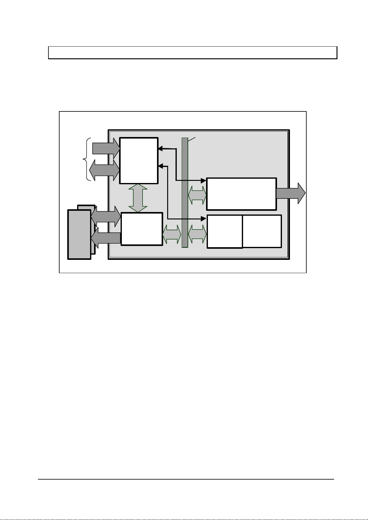
1.3 Block Diagram
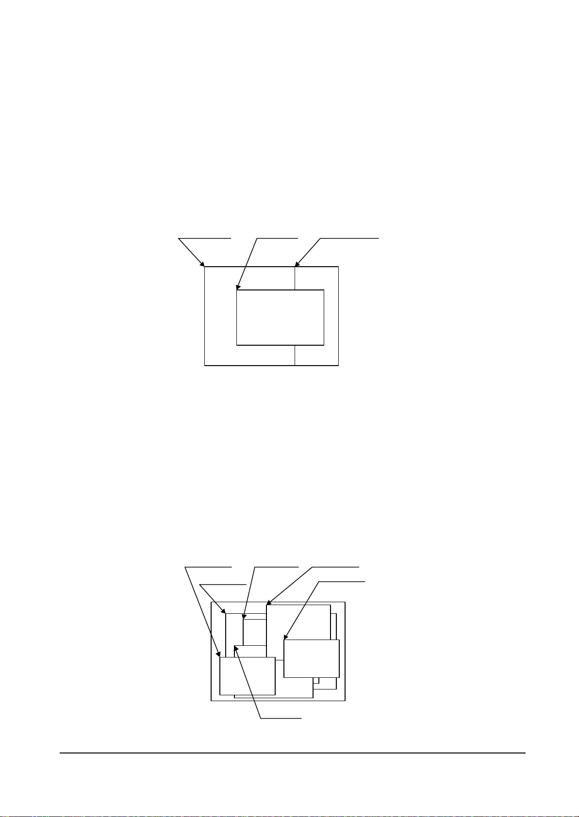
CORAL general block diagram is shown below:
Please note that the capture controller is deleted from this figure in Coral-LQ.
External
Bus of
Host CPU
A2-25
Host
Interface
D0 -31
Pixel Bus
Display Controller
D RGB
or
MD0-31/63
MA0-14
External
Memory
Controller
Geometry
Engine
2D/3D
Rendering
Engine
SDRAM
FCRAM
Fig.1.1 CORAL Block Diagram
MB86293 CORAL_LQ
Graphics Controller 12
Specifications Rev. 1.1
Page 13

FUJITSU LIMITED
PRELIMINARY and CONFIDENTIAL
1.4 Functional Overview
1.4.1 Host CPU interface
Supported CPU
Coral can be connected to SH3 and SH4 manufactured by HITACHI, V832 by NEC, SPARClite
(MB86833) by Fujitsu.
External Bus Clock
Can be connected at max. 100 MHz (when using SH4 interface)
Ready Mode
Supports normal ready/not ready.
Endian
Supports little endian.
Access Mode
SRAM interface
FIFO interface (transfer destination address fixed)
DMA transfer
Supports 1-double word (32 bits) /8-double word (32 bytes) (only SH4) for transfer unit.
ACK used/unused mode can be selected as protocol (only for DAM in dual address mode)
Supports dual address/mode single address mode (only SH4).
Supports cycle steel/burst.
Supports local display list transfer.
Interrupt
Vertical (frame) synchronous detection
Field synchronous detection
External synchronous error detection
Drawing command error
Drawing command execution end
MB86293 CORAL_LQ
Graphics Controller 13
Specifications Rev. 1.1
Page 14
FUJITSU LIMITED
PRELIMINARY and CONFIDENTIAL
Switching internal operating frequency
Switch the operating frequency immediately after a reset (before rewriting MMR mode register of
external memory interface).
Any operating frequency can be selected from the five combinations shown in Table 2-6.
Table 1-1 Frequency Setting Combinations
Clock for geometry engine Clock for other than geometry engine
166 MHz 133 MHz
166 MHz 100 MHz
133 MHz 133 MHz
133 MHz 100 MHz
100 MHz 100 MHz
The following relationship is disabled: Clock for geometry engine < Clock for other than geometry
engine
MB86293 CORAL_LQ
Graphics Controller 14
Specifications Rev. 1.1
Page 15
FUJITSU LIMITED
PRELIMINARY and CONFIDENTIAL
1.4.2 External memory interface
SDRAM or FCRAM can be connected.
64 bits or 32 bits can be selected for data bus.
Max. 133 MHz is available for operating frequency.
Connectable memory configuration is as shown below.
External Memory Configuration
Type Data bus width Use count Total capacity
FCRAM 16 Mbits (x 16 Bits) 32 Bits 2 4 Mbytes
FCRAM 16 Mbits (x16 Bits) 64 Bits 4 8 Mbytes
SDRAM 64 Mbits (x32 Bits) 32 Bits 1 8 Mbytes
SDRAM 64 Mbits (x32 Bits) 64 Bits 2 16 Mbytes
SDRAM 64 Mbits (x16 Bits) 32 Bits 2 16 Mbytes
SDRAM 64 Mbits (x16 Bits) 64 Bits 4 32 Mbytes
SDRAM 128 Mbits (x32 Bits) 32 Bits 1 16 Mbytes
SDRAM 128 Mbits (x32 Bits) 64 Bits 2 32 Mbytes
SDRAM 128 Mbits (x16 Bits) 32 Bits 2 32 Mbytes
SDRAM 128 Mbits (x16 Bits) 64 Bits 4 64 Mbytes
SDRAM 256 Mbits (x16 Bits) 32 Bits 2 64 Mbytes
MB86293 CORAL_LQ
Graphics Controller 15
Specifications Rev. 1.1
Page 16

FUJITSU LIMITED
PRELIMINARY and CONFIDENTIAL
1.4.3 Display controller
Video data output
Each 6-bit digital video output is provided.
Screen resolution
LCD panels with wide range of resolutions are supported by using a programmable timing generator as
follows:
Screen Resolutions
Resolutions
1024 × 768
1024 × 600
800 × 600
854 × 480
640 × 480
480 × 234
400 × 234
320 × 234
Hardware cursor
Coral supports two hardware cursor functions. Each of these hardware cursors is specified as a 64 ×
64-pixel area. Each pixel of these hardware cursors is 8 bits and uses the same look-up table as
indirect color mode.
Double buffer method
Double buffer method in which drawing window and display window is switched in units of 1 frame
enables the smooth animation.
Flipping (switching of display window area) is performed in synchronization with the vertical blanking
period using program.
Scroll method
Independent setting of drawing and display windows and their starting position enables the smooth
scrolling.
Display colors
• Supports indirect color mode which uses the look-up table (color palette) in 8 bits/pixels.
• Entry for look -up table (color palette) corresponds to color code for 8 bits, in other words, 256. Color
data is each 6 bits of RGB. Consequently, 256 colors can be displayed out of 260,000 colors.
• Supports direct color mode which specifies RGB with 16 bits/pixels.
MB86293 CORAL_LQ
Graphics Controller 16
Specifications Rev. 1.1
Page 17
FUJITSU LIMITED
L1 (WX, WY)
PRELIMINARY and CONFIDENTIAL
Overlay
Compatibility mode
Up to four extra layers (C, W, M and B) can be displayed overlaid.
The overlay position for the hardware cursors is above/below the top layer (C).
The transparent mode or the blend mode can be selected for overlay.
The M- and B-layers can be split into separate windows.
Window display can be performed for the W-layer.
Two palettes are provided: C-layer and M-/B-layer.
The W-layer is used as the video input layer.
L0, L2, L4 (0,0)
L3, L5 (HDB+1, 0)
Window mode
• Up to six screens (L0 to 5) can be displayed overlaid.
• The overlay sequence of the L0- to L5-layers can be changed arbitrarily.
• The overlay position for the hardware cursors is above/below the L0-layer.
• The transparent mode or the blend mode can be selected for overlay.
• The L5-layer can be used as the blend coefficient plane (8 bits/pixel).
• Window display can be performed for all layers.
• Four palettes corresponded to L0 to 3 are provided.
• The L1-layer is used as the video input layer.
• Background color display is supported in window display for all layers.
L0 (L0WX, L0WY)
L5 (L5WX, L5WY)
L4 (L4WX, L4WY)
L2 (L2WX, L2WY)
L1 (L1WX, L1WY)
L3 (L3WX, L3WY)
MB86293 CORAL_LQ
Graphics Controller 17
Specifications Rev. 1.1
Page 18

FUJITSU LIMITED
PRELIMINARY and CONFIDENTIAL
1.4.4 Geometry processing
Coral has a geometry engine for performing the numerical operations required for graphics processing.
The geometry engine uses the floating-point format for highly precise operations. It selects the required
geometry processing according to the set drawing mode and primitive type and executes processing to
the final drawing.
Primitives
Point, line, line strip, independent triangle, triangle strip, triangle fan, and arbitrary polygon are
supported.
MVP Transformation
MVP Transformation
Setting a 4 × 4 transformation matrix enables transformation of a 3D model view projection.
Two-dimensional affine transformation is also possible.
Clipping
Clipping stops drawing of figures outside the window (field of view). Polygons (including concave
shapes) can also be clipped.
Culling
Triangles on the back are not drawn.
3D-2D Transformation
This functions transforms 3D coordinates (normalization) into 2D coordinates in orthogonal or
perspective projections.
View port transformation
This function transforms normalized 2D coordinates into drawing (device) coordinates.
Primitive setup
This function automatically performs a variety of slope computations, etc., based on transforming
vertex data into coordinates and prepares for rendering (setup).
Log output of device coordinates
The view port conversion results are output to the local memory.
MB86293 CORAL_LQ
Graphics Controller 18
Specifications Rev. 1.1
Page 19

FUJITSU LIMITED
PRELIMINARY and CONFIDENTIAL
1.4.5 2D Drawing
2D Primitives
Coral can perform 2D drawing for graphics memory (drawing plane) in direct color mode or indirect
color mode.
Bold lines with width and broken lines can be drawn. With anti-aliasing smooth diagonal lines also
can be drawn.
A triangle can be tiled in a single color or 2D pattern (tiling), or mapped with a texture pattern by
specifying coordinates of the 2D pattern at each vertex (texture mapping). At texture mapping,
drawing/non-drawing can be set in pixel units. Moreover, transparent processing can be performed
using alpha blending. When drawing in single color or tiling without Gouraud shading or texture
mapping, high-speed 2DLine and high -speed 2DTriangle can be used. Only vertex coordinates are
set for these primitives. High-speed 2DTriangle is also used to draw polygons.
2D Primitives
Primitive type Description
Point Plots point
Line Draws line
Bold line strip
(provisional name)
Triangle Draws triangle
High-speed 2DLine Draws lines
Arbitrary polygon Draws arbitrary closed polygon containing concave shapes
Draws continuous bold line
This primitive is used when interpolating the bold line joint.
Compared to line, this reduces the host CPU processing load.
consisting of vertices
Arbitrary polygon drawing
Using this function, arbitrary closed polygon containing concave shapes consisting of vertices can be
drawn. (There is no restriction on the count of vertices, however, the polygon with its sides crossed
are not supported.) In this case, as a work area for drawing, polygon drawing flag buffer is used on
the graphics memory. In drawing polygon, draw triangle for polygon drawing flag buffer using
high-speed 2DTriangle. Decide any vertex as a starting point to draw triangle along the periphery. It
enables you to draw final polygon form in single color or with tiling/texture mapping in a drawing frame.
MB86293 CORAL_LQ
Graphics Controller 19
Specifications Rev. 1.1
Page 20

FUJITSU LIMITED
PRELIMINARY and CONFIDENTIAL
BLT/Rectangle drawing
This function draws a rectangle using logic operations. It is used to draw pattern and copy the image
pattern within the drawing frame. It is also used for clearing drawing frame and Z buffer.
BLT Attributes
Attribute Description
Raster operation Selects two source logical operation mode
Transparent processing Performs BLT without drawing pixel consistent with the
transparent color.
Alpha blending The alpha map and source in the memory is subjected to alpha
blending and then copied to the destination.
Pattern (Text) drawing
This function draws a binary pattern (text) in a specified color.
Pattern (Text) Drawing Attributes
Attribute Description
Enlarge Vertically 2 × 2
Horizontally × 2
Vertically and Horizontally × 2
Shrink Vertically 1/2 × 1/2
Horizontally 1/2
Vertically and Horizontally 1/2
Drawing clipping
This function sets a rectangle frame in drawing frame to prohibit the drawing of the outside the frame.
MB86293 CORAL_LQ
Graphics Controller 20
Specifications Rev. 1.1
Page 21

FUJITSU LIMITED
PRELIMINARY and CONFIDENTIAL
1.4.6 3D Drawing
3D Primitives
This function draws 3D objects in drawing memory in the direct color mode.
3D Primitives
Primitive Description
Point Plots 3D point
Line Draws 3D line
Triangle Draws 3D triangle
Arbitrary polygon Draws arbitrary closed polygon containing concave shapes
consisting of vertexes
3D Drawing attributes
Texture mapping with bi-linear filtering/automatic perspective correction and Gouraud shading provides
high-quality realistic 3D drawing. A built-in texture mapping unit performs fast pixel calculations.
This unit also delivers color blending between the shading color and texture color.
Hidden plane management
Coral supports the Z buffer for hidden plane management.
MB86293 CORAL_LQ
Graphics Controller 21
Specifications Rev. 1.1
Page 22

FUJITSU LIMITED
PRELIMINARY and CONFIDENTIAL
1.4.7 Special effects
Anti-aliasing
Anti-aliasing manipulates line borders of polygons in sub-pixel units and blend the pre -drawing pixel
color with color to make the jaggies be seen smooth. It is used as a functional option for 2D drawing
(in direct color mode only).
Bold line and broken line drawing
This function draws lines of a specific width and a broken line.
Line Drawing Attributes
Attribute Description
Line width Selectable from 1 to 32 pixels
Broken line Set by 32 bit or 24 bit of broken line pattern
• Supports the verticality of starting and ending points.
• Supports the verticality of broken line pattern.
• Interpolation of bold line joint supports the following modes:
(1) Broken line pattern reference address fix mode
→ The same broken line pattern is kept referencing for the period of some pixels starting from the
joint and the starting point for the next line.
(2) No interpolation
• Supports the equalization of the width of bold lines.
• Supports the bold line edging.
• Not support the Anti-aliasing of dashed line patterns.
• For a part overlaid due to connection of bold lines, natural overlay can be represented by providing depth
information. (Z value).
Shading
Supports the shading primitive.
Drawing is performed to the body primitive coordinates (X, Y) with an offset as a shade. At this drawing,
the Z buffer is used in order to differentiate between the body and shade.
MB86293 CORAL_LQ
Graphics Controller 22
Specifications Rev. 1.1
Page 23

FUJITSU LIMITED
PRELIMINARY and CONFIDENTIAL
Alpha blending
Alpha blending blends two image colors to provide a transparent effect. CORAL supports two types
of blending; blending two different colors at drawing, and blending overlay planes at display.
Transparent color is not used for these blending options.
There are two ways of specifying alpha blending for drawing:
(1) Set a transparent coefficient to the register; the transparent coefficient is applied for transparency
processing of one plane.
(2) Set a transparent coefficient for each vertex of the plane; as with Gouraud shading, the transparent
coefficient is linear-interpolated to perform transparent processing in pixel units.
In addition to the above, the following settings can be performed at texture mapping. When the most
significant bit of each texture cell is 1, drawing or transparency can be set. When the most significant
bit of each texture cell is 0, non-drawing can be set.
Alpha Blending
Type Description
Drawing Transparent ratio set in particular register
While one primitive (polygon, pattern, etc.), being drawn,
registered transparent ratio applied
A transparent coefficient set for each vertex. A
linear-interpolated transparent coefficient applied.
This is possible only in direct color mode.
Overlay display Blends top layer pixel color with lower layer pixel color
Transparent coefficient set in particular register
Registered transparent coefficient applied during one frame
scan
Gouraud Shading
Gouraud shading can be used in the direct color mode to provide 3D object real shading and color
gradation.
Gray Scale Gouraud Shading
Gray scale gouraud shading can be used in the in-direct color(8bit/pixel) mode to draw a blend
coefficient layer.
MB86293 CORAL_LQ
Graphics Controller 23
Specifications Rev. 1.1
Page 24

FUJITSU LIMITED
PRELIMINARY and CONFIDENTIAL
Texture mapping
Coral supports texture mapping to map an image pattern onto the surface of plane. The texture
pattern can be laid out in the graphics memory. In this case, max. 4096 × 4096 pixels can be used.
For drawing 8-bit color, only point sampling can be specified for texture interpolation; only de -curl can
be specified for the blend mode.
Texture Mapping
Function Description
Filtering Point sample
Bi-linear filter
Coordinate s correction Linear
Perspective
Blend De-curl
Modulate
Stencil
Alpha blend Normal
Stencil
Stencil alpha
Wrap Repeat
Cramp
Border
MB86293 CORAL_LQ
Graphics Controller 24
Specifications Rev. 1.1
Page 25

FUJITSU LIMITED
PRELIMINARY and CONFIDENTIAL
1.4.8 Others
Drawing color
8-bit indirect color and 16-bit direct color are supported as a drawing input data.
Top-left rule non-applicable mode
In addition to the top-left rule applicable mode in which the triangle borders are compatible with
CREMSON, the top-left rule non-applicable mode can be used. (In case of non-top-left polygon
drawing, an object has to be in a geometry clipping area.)
Caution: Use perspective correct mode when use texture at the top-left rule non-applicable mode.
Top-left rule non-applicable primitives cannot use Geometry clip function.
Non-top-left-part’s pixel quality is less than body. (using approximate calculation)
MB86293 CORAL_LQ
Graphics Controller 25
Specifications Rev. 1.1
Page 26
FUJITSU LIMITED
XCS
XRD
Clock
CKM
PRELIMINARY and CONFIDENTIAL
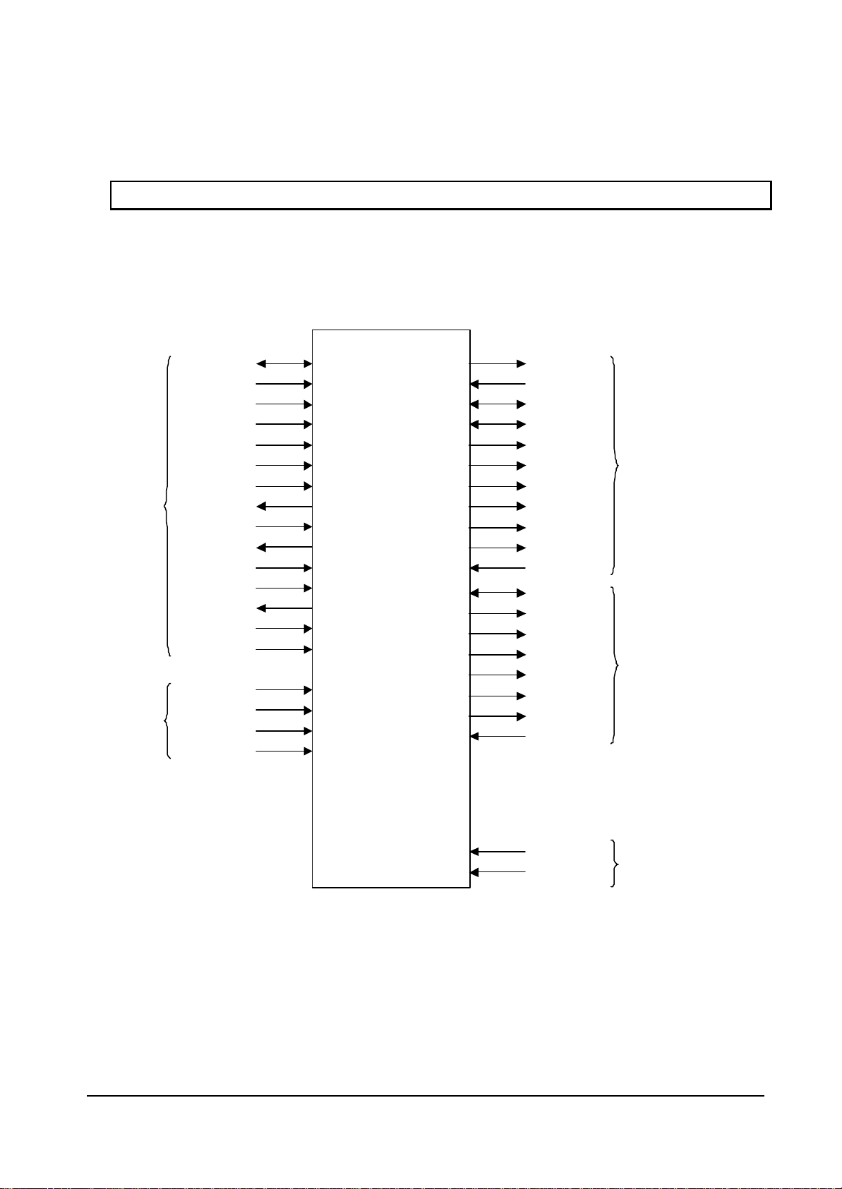
2 PINS
2.1 Signals
2.1.1 Signal lines
Host CPU
interface
D0-31
A2-25
BCLKI
XRST
XWE0-3
XRDY
XBS
DREQ
DRACK
DTACK
XINT
RDY_MODE
BS_MODE
CLK
CLKSEL0-1
DCLKO
DCKLI
HSYNC
VSYNC
CSYNC
DISPE
GV
R2-7
CORAL
Graphics Controller
HQFP256
S
G2-7
B2-7
XRGBEN
MD0-63
MA0-14
MRAS
MCAS
MWE
MDQM0-7
MCLKO
MCLKI
TESTH
TRST
Video output
interface
Graphics memory
interface
Test
MB86293 CORAL_LQ
Graphics Controller 26
Specifications Rev. 1.1
Fig. 2.1 CORAL Signal Lines
Page 27
FUJITSU LIMITED
PRELIMINARY and CONFIDENTIAL
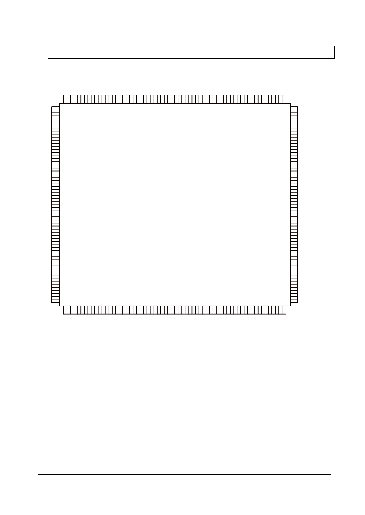
2.2 Pin Assignment
2.2.1 Pin assignment diagram
DTACK
XWE0
VDDL
XWE1
XWE2
XWE3
A25
A24
A23
A22
A21
A20
A19
A18
A17
A16
A15
VDDL
A14
A13
A12
A11
A10A9A8A7A6A5A4A3A2
256
255
254
253
252
251
250
249
248
247
246
245
244
243
242
241
240
239
238
237
236
235
234
233
232
231
DRACK 1
BS_MODE 2 191 DG7
3 190 DG6
4
XINT
DREQ 5 188 DG4
XRDY 6 187 DG3
VDDH 7
VDDL 8 185 DB7
BCLKI 9 184 VDDL
10
XCS
XRD 11 182 DB5
XBS 12 181 DB4
CKM 13 180 DB3
MODE0 14 179 DB2
MODE1 15 178 VDDH
MODE2 16 177 VSS
XRST 17 176 VSS
VSS 18 175 MD63/R1
VSS 19 174 MD62/R0
D0 20 173 MD61/G1
D1 21 172 MD60/G0
D2 22 171 MD59/B1
D3 23
VDDL 24 169 MD57
D4 25 168 VDDL
D5 26
VDDH 27 166 MD55
D6 28 165 MD54
D7 29
D8 30 163 MD52
D9 31 162 MD51
D10 32
D11 33 160 MD49
D12 34 159 MD48
D13 35
D14 36 157 TESTH
D15 37 156 MD47
D16 38 155 MD46
D17 39 154 MD45
VDDL 40 153 MD44
D18 41 152 VDDL
VDDH 42 151 MD43
D19 43 150 MD42
D20 44 149 MD41
D21 45
D22 46 147 VSS
D23 47 146 VSS
D24 48
D25 49 144 MD38
D26 50 143 MD37
D27 51
D28 52 141 MD35
D29 53 140 MD34
D30 54
D31 55 138 MD32
VDDL 56 137 XRGBEN
VDDH 57
VSS 58 135 VDDL
VSS 59 134 VSS
MD0 60 133 VSS
MD1 61 132 MCLKI
MD2 62 131 VDDH
MD3 63 130 VSS
MD4 64 129 VSS
6566676869707172737475767778798081828384858687888990919293949596979899
MD5
MD6
MD7
MD8
MD9
VDDL
MD10
MD11
MD12
MD13
MD14
MD15
VDDH
MD16
MD17
MD18
VDDL
MD19
MD20
MD21
MD22
MD23
MD24
MD25
MD26
MD27
230
MD28
229
MD29
228
MD30
227
MD31
226
VDDL
CLKSEL0
VDDL
225
224
VSS
VSS
CLKSEL1
VSS
223
222
VDDH
DQM0
VSS
221
100
DQM1
CLK
220
101
DQM2
PLLVDD
PLLVSSSTRST
219
218
102
103
MA0
DQM3
TESTH
TESTH
DCLKI
VSS
VSS
TESTH
VDDL
TESTH
VSYNC
HSYNC
VSS
VSS
CSYNCGVDE
DCLKO
VDDH
DR7
DR6
DR5
DR4
VDDL
DR3
217
216
215
214
213
212
211
210
209
208
207
206
205
204
203
202
201
200
199
198
197
196
195
194
193
192 DR2
189 DG5
186 DG2
183 DB6
170 MD58/B0
167 MD56
164
161
158
148
145 MD39
142 MD36
139
136
104
105
106
107
108
109
110
111
112
113
114
115
116
117
118
119
120
121
122
123
124
125
126
127
128
MA1
MA2
MA3
MA4
MA5
MA6
MA7
MA8
VDDL
MA9
MA10
MA11
MA12
MA13
MA14
VDDH
MRAS
MCAS
MWE
DQM4
DQM5
DQM6
DQM7
VDDL
MCLKO
MD53
MD50
TESTH
MD40
MD33
TESTH
Note: The MODE2 signal used for Orchid is changed as shown below.
MODE2 signal for Orchid → RDY_MODE signal for Coral
MB86293 CORAL_LQ
Graphics Controller 27
Specifications Rev. 1.1
Page 28
FUJITSU LIMITED
64
MD4
128
MCLKO
192
DR2
256
DTACK
PRELIMINARY and CONFIDENTIAL
2.2.2 Pin assignment table
No. Name No. Name No. Name No. Name
1 DRACK 65 MD5 129 VSS 193 DR3
2 BS_MODE 66 VDDL 130 VSS 194 VDDL
3 RDY_MODE 67 MD6 131 VDDH 195 DR4
4 XINT 68 MD7 132 MCLKI 196 DR5
5 DREQ 69 MD8 133 VSS 197 DR6
6 XRDY 70 MD9 134 VSS 198 DR7
7 VDDH 71 MD10 135 VDDL 199 VDDH
8 VDDL 72 MD11 136 TESTH 200 DCLKO
9 BCLKI 73 MD12 137 XRGBEN 201 DE
10 XCS 74 MD13 138 MD32 202 GV
11 XRD 75 MD14 139 MD33 203 CSYNC
12 XBS 76 MD15 140 MD34 204 VSS
13 CKM 77 VDDH 141 MD35 205 VSS
14 MODE0 78 MD16 142 MD36 206 HSYNC
15 MODE1 79 MD17 143 MD37 207 VSYNC
16 MODE2 80 MD18 144 MD38 208 TESTH
17 XRST 81 VDDL 145 MD39 209 VDDL
18 VSS 82 MD19 146 VSS 210 TESTH
19 VSS 83 MD20 147 VSS 211 VSS
20 D0 84 MD21 148 MD40 212 VSS
21 D1 85 MD22 149 MD41 213 DCLKI
22 D2 86 MD23 150 MD42 214 TESTH
23 D3 87 MD24 151 MD43 215 TESTH
24 VDDL 88 MD25 152 VDDL 216 TRST
25 D4 89 MD26 153 MD44 217 S
26 D5 90 MD27 154 MD45 218 PLLVSS
27 VDDH 91 MD28 155 MD46 219 PLLVDD
28 D6 92 MD29 156 MD47 220 CLK
29 D7 93 MD30 157 TESTH 221 VSS
30 D8 94 MD31 158 TESTH 222 VSS
31 D9 95 VDDL 159 MD48 223 CLKSEL1
32 D10 96 VSS 160 MD49 224 VDDL
33 D11 97 VSS 161 MD50 225 CLKSEL0
34 D12 98 VDDH 162 MD51 226 A2
35 D13 99 DQM0 163 MD52 227 A3
36 D14 100 DQM1 164 MD53 228 A4
37 D15 101 DQM2 165 MD54 229 A5
38 D16 102 DQM3 166 MD55 230 A6
39 D17 103 MA0 167 MD56 231 A7
40 VDDL 104 MA1 168 VDDL 232 A8
41 D18 105 MA2 169 MD57 233 A9
42 VDDH 106 MA3 170 MD58/B0 234 A10
43 D19 107 MA4 171 MD59/B1 235 A11
44 D20 108 MA5 172 MD60/G0 236 A12
45 D21 109 MA6 173 MD61/G1 237 A13
46 D22 110 MA7 174 MD62/R0 238 A14
47 D23 111 VDDL 175 MD63/R1 239 VDDL
48 D24 112 MA8 176 VSS 240 A15
49 D25 113 MA9 177 VSS 241 A16
50 D26 114 MA10 178 VDDH 242 A17
51 D27 115 MA11 179 DB2 243 A18
52 D28 116 MA12 180 DB3 244 A19
53 D29 117 MA13 181 DB4 245 A20
54 D30 118 MA14 182 DB5 246 A21
55 D31 119 VDDH 183 DB6 247 A22
56 VDDL 120 MRAS 184 VDDL 248 A23
57 VDDH 121 MCAS 185 DB7 249 A24
58 VSS 122 MWE 186 DG2 250 A25
59 VSS 123 DQM4 187 DG3 251 XWE3
60 MD0 124 DQM5 188 DG4 252 XWE2
61 MD1 125 DQM6 189 DG5 253 XWE1
62 MD2 126 DQM7 190 DG6 254 VDDL
63 MD3 127 VDDL 191 DG7 255 XWE0
MB86293 CORAL_LQ
Graphics Controller 28
Specifications Rev. 1.1
Page 29

FUJITSU LIMITED
PRELIMINARY and CONFIDENTIAL
Notes
VSS/PLLVSS : Ground
V
: 3.3-V power supply
DDH
V
/PLLVDD : 1.8-V power supply
DDL
PLLVDD : PLL power supply
OPEN : Do not connect anything.
TESTH : Input a 3.3 V-power supply.
- It is recommended that PLLVDD should be isolated on the PCB.
- Insert a bypass capacitor with good high frequency characteristics between the power supply and
ground.
Place the capacitor as near as possible to the pin.
MB86293 CORAL_LQ
Graphics Controller 29
Specifications Rev. 1.1
Page 30
FUJITSU LIMITED
DMA transfer strobe signal (XTC is used in the V832 mode.
PRELIMINARY and CONFIDENTIAL
2.3 Pin Function
2.3.1 Host CPU interface
Table 2-1 Host CPU Interface Pins
Pin name I/O Description
MODE0-2 Input Host CPU mode select
RDY_MODE Input Normally ready, Not ready select
BS_MODE Input BS signal with/without select
XRST Input Hardware reset
D0-31 In/Out Host CPU bus data
A2-A25 Input Host CPU bus address (In the V832 mode, A[24] is
BCLKI Input Host CPU bus clock
XBS Input Bus cycle start signal
XCS Input Chip select signal
XRD Input Read strobe signal
XWE0 Input Write strobe for D0 to D7 signal
XWE1 Input Write strobe for D8 to D15 signal
XWE2 Input Write strobe for D16 to D23 signal
XWE3 Input Write strobe for D24 to D31 signal
XRDY Output
Tri-state
DREQ Output DMA request signal (This signal is low-active in both the SH
DRACK/DMAAK Input Acknowledge signal in response to DMA request (DMAAK is
DTACK/XTC Input
XINT Output Interrupt signal issued to host CPU (In the SH mode, and
connected to XMWR.)
Wait request signal (In the SH3 mode, when this signal is
“0”, it indicates the wait state; in the SH4, V832 and
SPARClite modes, when this signal is “1”, it indicates the
wait state.)
mode and V832 mode.)
used in the V832 mode; this signal is high-active in both the
SH mode and V832 mode.)
In the SH mode, this signal is high-active; in the V832 mode,
it is low-active.)
SPARClite this signal is low-active; in the V832 mode, it is
high-active)
MB86293 CORAL_LQ
Graphics Controller 30
Specifications Rev. 1.1
Page 31

FUJITSU LIMITED
PRELIMINARY and CONFIDENTIAL
• Coral can be connected to the Hitachi SH4 (SH7750), SH3 (SH7709) NEC V832 and Fujitsu SPARClite
(MB86833) without external circuit. In the SRA M interface mode, Coral can be used with any other CPU
as well. The host CPU is specified by the MODE0 to 2 pins.
MODE 2 MODE 1 MODE 0 CPU
L L
L L
L H
L H H SPARClite
H X X Reserved
L SH3
H SH4
L V832
When the bus cycle terminates, a ready signal level can be set . When using the RDY_MODE signal at
“High” level, set two cycles as the CPU software wait of the CPU. (When BS_MODE = “High” level, set
the CPU software wait to three cycles.)
RDY_MODE Ready signal mode
L When the bus cycle terminates, sets the XRDY signal to the ‘not ready’ level.
H When the bus cycle terminates, sets the XRDY signal to the ‘ready’ level.
A CPU with no BS (Bus Start) pin can be used. Setting can be performed in all CPU modes.
Connection can be made to a CPU with no BS signal by setting the BS_MODE signal to “High” level.
When not using the BS signal, fix the BS pin of CORAL at “High” level.
When using the BS_MODE signal as “High” level in the normally ready mode, set the CPU software wait
to three cycles.
BS_MODE BS signal mode
L Connect to a CPU with the BS signal
H Connect to a CPU without the BS signal
The data signal is 32 bits (fixed).
The address signal is 32 bits (per one double-word) × 24, and has a 64-Mbyte address field. (16-MByte
address space is provided for V832 and SPARClite.)
The external bus operating frequency is up to 100 MHz.
In the SH4, V832, and SPARClite modes, when the XRDY signal is low, it is in the ready state. However,
in the SH3 mode, when the XRDY signal is low, it is in the wait state. This signal is a tri -state output that
is synchronized with the rising edge of BCLKI.
DMA data transfer is supported using an external DMA controller.
An interrupt signal is generated to the host CPU.
The XRST input must be kept low for at least 300 µs after setting the S (PLL reset) signal to high.
In the V832 mode, Coral signals are connected to the V832 CPU as follows:
CORAL Pins V832 Signals
A24 XMWR
DTACK XTC
DRACK DMAAK
MB86293 CORAL_LQ
Graphics Controller 31
Specifications Rev. 1.1
Page 32

FUJITSU LIMITED
PRELIMINARY and CONFIDENTIAL
2.3.2 Video output interface
Pin name I/O Description
DCLKO Output Dot clock signal for display
DCLKI Input Dot clock signal input
HSYNC I/O Horizontal sync signal output
VSYNC I/O Vertical sync signal output
CSYNC Output Composite sync signal output
DISPE Output Display enable period signal
GV Output Graphics/video switch
R2-7 Output Digital picture (R) output
G2-7 Output Digital picture (G) output
B2-7 Output Digital picture (B) output
XRGBEN Input Signal to switch between RGB1 and 0 output/memory bus
Table 2-2 Video Output Interface Pins
Horizontal sync input <in external sync mode>
Vertical sync input <in external sync mode>
(MD 63 to 58)
6-bit display data is output as standard for R, G, and B. Depending on the condition, 8-bit display data
can also be output for R, G, and B. Fixing XRGBEN at 0, R0, 1, G0, 1, and B0, 1 can be output to MD62,
63, MD60, 61, and MD58, 59 respectively. When 8-bit output is selected for R, G, and B, only the 32-bit
mode can be used for the memory bus width mode.
Additional setting of external circuits can generate composite video signal.
Synchronous to external video signal display can be performed.
Either mode which is synchronous to DCLKI signal or one which is synchronous to dot clock, as for
normal display can be selected.
Since HSYNC and VSYNC signals are set to input state after reset, these signals must be pulled up LSI
externally.
The GV signal switches graphics and video at chroma key operation. When video is selected, the “Low”
level is output.
MB86293 CORAL_LQ
Graphics Controller 32
Specifications Rev. 1.1
Page 33

FUJITSU LIMITED
PRELIMINARY and CONFIDENTIAL
2.3.3 Graphics memory interface
Table 2-3 Graphics memory interface pins
Pin name I/O Description
MD0 to 57 I/O Graphics memory bus data
MD58 to 63/RGB I/O Graphics memory bus data or RGB0 to 1 output
MA0 to 14 Output Graphics memory bus data
MRAS Output Row address strobe
MCAS Output Column address strobe
MWE Output Write enable
MDQM0 to 7 Output Data mask
MCLK0 Output Graphics memory clock output
MCLK1 Input Graphics memory clock input
Connect the interface to the external memory used as memory for image data. The interface can be
connected to 64-/128-/256-Mbit SDRAM (16- or 32-bit length data bus) without using any external
circuit.
64 bits or 32 bits can be selected for the memory bus data. When 32 -bit memory bus data is used
and 6-bit output is used for R, G, and B (XRGBEN pin = 1), set MD32 to 63 and MDQM4 to 7 to the
open state. When 32 -bit memory bus data is used and 8-bit output is used for R, G, and B (XRGBEN
pin = 0), set MD32 to 39 to “High” level input and set MD40 to 57 and MDQM4 to 7 to the open state.
Connect MCLKI to MCLK0.
When XRGBEN is fixed at “1”, MD58 to 63 can be used as graphics memory bus data.
When XRGBEN is fixed at “0”, MD58 to 63 can be used as digital RGB0 to 1 outputs.
MB86293 CORAL_LQ
Graphics Controller 33
Specifications Rev. 1.1
Page 34

FUJITSU LIMITED
PRELIMINARY and CONFIDENTIAL
2.3.4 Clock input
Table 2-4 Clock Input Pins
Pin name I/O Description
CLK Input Clock input signal
S Input PLL reset signal
CKM Input Clock mode signal
CLKSEL [1:0] Input Clock rate select signal
Inputs source clock for internal operation clock and display dot clock. Normally, 4 Fsc (= 14.31818 MHz:
NTSC) is input. An internal PLL generates the internal operation clock of 166 MHz/133 MHz and the
display base clock of 400 MHz.
CKM Clock mode
L Output from internal PLL selected
H Host CPU bus clock (BCLK1) selected
• When CKM = L, selects input clock frequency when built-in PLL used according to setting of CLKSEL pins
CLKSEL1 CLKSEL0
L L Inputs 13.5-MHz
L H Inputs 14.32-MHz
H L Inputs 17.73-MHz
H H Reserved
Input clock
frequency
clock frequency
clock frequency
clock frequency
Multiplication
rate
× 29 391.5 MHz
× 28 400.96 MHz
× 22 390.06 MHz
Display
reference clock
MB86293 CORAL_LQ
Graphics Controller 34
Specifications Rev. 1.1
Page 35

FUJITSU LIMITED
PRELIMINARY and CONFIDENTIAL
2.3.5 Test pins
Pin name I/O Description
TESTH Input Input 3.3-V power.
TRST Input This is the test reset signal.
2.3.6 Reset sequence
See Section 10.3.2.
Table 2-5 Test Pins
Before performing reset via S/XRST, perform reset
via this signal (TRST).
MB86293 CORAL_LQ
Graphics Controller 35
Specifications Rev. 1.1
Page 36

FUJITSU LIMITED
PRELIMINARY and CONFIDENTIAL
3 PROCEDURE OF THE HARDWARE INITIALIZATION
3.1 Hardware reset
1.Do the hardware reset. (see section 11.3.2)
2.After the hardware reset, set the CCF(Change of Frequency) register (section 9.2.1).
In being unstable cycle after the hardware reset, keep 32 bus cycles open.
3.Set the graphics memory interface register, MMR (Memory I/F Mode Register).
After setting the CCF register, take 200 us to set the MMR register.
In being unstable memory access cycle, keep 32 bus cycles open.
4.Other registers, except for the CCF register and the MMR register, should be set after
setting the CCF register.
In case of not using memory access, the MMR register could be set in any order after
the CCF register is set.
3.2 Re-reset
1. Reset XRST signal.
2. See section 3.1 for registers setting after the procedure of re-reset.
3.3 Software reset
1. Set the value of the SRST register (see section 9.2.1) for re-reset.
2. It is not necessary to reset the CCF register and the MMR register again.
MB86293 CORAL_LQ
Graphics Controller 36
Specifications Rev. 1.1
Page 37
FUJITSU LIMITED
PRELIMINARY and CONFIDENTIAL
4 HOST INTERFACE
4.1 Operation Mode
4.1.1 Host CPU mode
Select the host CPU by setting the MODE0 to MODE 2 signals as follows:
Table 4-1 CPU Type Setting
MODE 2 MODE 1 MODE 0 CPU
L L
L L
L H
L H H SPARClite
H X X Reserved
L SH3
H SH4
L V832
4.1.2 Ready signal mode
The MODE2 pin can be used to set the ready signal level when the bus cycle of the host CPU terminates.
For the normally not ready mode, set the software wait to 0 or 1 cycles. When using this device in the
normally ready mode, set the software wait to 2 cycles. When using this device in the normally not ready
mode, set the software wait to one cycle. (When BS_MODE = H, three cycles are needed for the
software wait.)
The ‘normally not ready mode’ is the mode in which the CORAL XRDY signal is always in the wait state
and Ready is returned only when read/write is ready.
The ‘normal ready mode’ is the mode in which the CORAL XRDY signal is always in the Ready state and
it is put into the wait state only when read/write cannot be performed immediately.
Table 4-2 Ready Signal Mode
RDY_MODE Ready signal operation
L
H
Recognizes XRDY signal as ‘not ready level’ and terminates bus cycle
(normally not ready mode)
Recognizes XRDY signal as ‘ready level’ and terminates bus cycle (norma lly
ready mode)
MB86293 CORAL_LQ
Graphics Controller 37
Specifications Rev. 1.1
Page 38

FUJITSU LIMITED
PRELIMINARY and CONFIDENTIAL
4.1.3 BS signal mode
Connection to a CPU without the BS signal can be made via the BS_MODE signal. This setting can be
performed for all CPU modes. To connect to a CPU without the BS signal, set the BS_MODE signal to
“High” level.
When not using the BS signal, fix the BS pin of CORAL at “High” level.
When using the BS_MODE signal as “High” level, with the normally ready mode established, set the CPU
software wait to three cycles.
Table 4-3 BS Signal Mode
BS_MODE Operation of BS signal
L Connects to CPU with BS signal
H Connects to CPU without BS signal
4.1.4 Endian
CORAL operates in little-endian mode. All the register address descriptions in the specifications are byte
address in little endian. When using a big-endian CPU, note that the byte-or word-addresses are
different from these descriptions.
MB86293 CORAL_LQ
Graphics Controller 38
Specifications Rev. 1.1
Page 39

FUJITSU LIMITED
PRELIMINARY and CONFIDENTIAL
4.2 Access Mode
4.2.1 SRAM interface
Data can be transferred to/from CORAL using SRAM access protocol. CORAL internal registers and
graphics memory are all mapped to the physical address area of the host processor.
CORAL uses hardware wait based on the XRDY signal, enabling the hardware wait setting of the host
CPU. When using the normally not ready mode, set the software wait to “1”. When using the normally
ready mode, set the software wait to “2”. (When using the BS_MODE signal as “High” level, with the
normally ready mode established, set the CPU software wait to three cycles.) Switch the ready mode
using the RDY_MODE signal.
CPU Read
The host processor reads data from internal registers and memory of CORAL in double-word (32 bit)
units. Valid data is output continuously while XRD and XCS are being asserted at a “Low” level after
XRDY has been asserted.
CPU Write
The host CPU writes data to internal registers and memory of CORAL in byte, word(16 bit) and
double-word( 32 bit) units.
4.2.2 FIFO interface (fixed transfer destination address)
This interface transfers display lists stored in host memory. Display list information is transferred
efficiently using a single address mode DMA transfer. Data can be transferred to FIFO in relation to
FIFO buffer area mapped in memory area using SRAM interface or dual address mode.
MB86293 CORAL_LQ
Graphics Controller 39
Specifications Rev. 1.1
Page 40

FUJITSU LIMITED
PRELIMINARY and CONFIDENTIAL
4.3 DMA Transfer
4.3.1 Data transfer unit
DMA transfer is performed in double-word (32 bits) units or 8 double-word (32 bytes) units. Byte and
word access is not supported.
Note: 8 double-word transfer is supported only in the SH4 mode.
4.3.2 Address mode
Dual address mode (mode using ACK)
DMA is performed at memory-to-memory transfer between host memory and registers mapped in
memory space or graphics memory (destination). Both the host memory address and CORAL is used.
In the SH4 mode, the 1 double -word transfer (32 bits) and 8 double-word transfer (32 bytes) can be
used.
When the CPU transfer destination address is fixed, data can also be transferred to the FIFO interface.
However, in this case, even the SH4 mode supports only the 1 double-word transfer.
DREQ and DRACK pins and SRAM interface signals are used. In V832, the DREQ, DMAAK, and
XTC pins and SRAM interface signals are used.
Note: The SH3 mode supports the direct address mode; it does not support the indirect address
mode.
Dual address mode (mode not using ACK)
When not using the ACK signal with the dual address mode established, set bit3 at HostBase+0004h
(DNA: Dual address No Ack mode) to 1.
When the ACK is not used, the DREQ signal is in the edge mode and the DREQ signal is negated per
transfer and then reasserted it in the next cycle. If processing cannot be performed immediately
inside CORAL, the DREQ signal remains negated.
The transfer count register (DTC) of CORAL is not used, so in order to end DMA transfer, write “1” to
the DMA transfer stop register (DTS) from the CPU.
Note 1: In the dual DMA mode (mode without ACK), the destination address can be used only for the
FIFO.
In DMA transfer to the graphics memory, etc., use the dual DMA mode.
Note 2: DMA read is not supported.
Single address mode (FIFO interface)
Data is transferred between host memory (source) and FIFO (destination). Only the address output
from the host memory is used, and the data is transferred to the FIFO. This mode does not support
data write to the host memory. When the FIFO is full, the DMA transfer is suspended.
The 1 double-word transfer (32 bits) and the 8 double-word transfer (32 B) can be used.
DREQ, DTACK, and DRACK signal are used.
Note: The single-address mode is supported only in the SH4 mode.
MB86293 CORAL_LQ
Graphics Controller 40
Specifications Rev. 1.1
Page 41

FUJITSU LIMITED
PRELIMINARY and CONFIDENTIAL
4.3.3 Bus mode
Coral supports the DMA transfer cycle steal mode and burst mode according to setting of external DMA
mode.
Cycle steal mode (In the V832 mode, the burst mode is called the single transfer mode.)
In the cycle steal mode, the right to use the bus is obtained or released at every data transfer of 1 unit.
The DMA transfer unit can be selected from between the 1 double-word (32 bits) and 8 double-words
(32 B).
Burst mode (In the V832 mode, the burst mode is called the demand transfer mode.)
When DMA transfer is started, the right to use the bus is acquired and the transfer begins. The data
transfer unit can be selected from between the 1 double-word (32 bits) and 8 double-words (32 B).
Note: When performing DMA transfer in the dual-address mode, a function for automatically negating
DREQ is provided based on the setting of the DBM register.
4.3.4 DMA transfer request
Single-address mode
DMA is started when the CORAL issues an external request to DMAC of the host processor.
Set the trans fer count in the transfer count register of the CORAL and then issue DREQ.
Fix the CPU destination address to the FIFO address.
Dual-address mode
DMA is started by two procedures: CORAL issues an external request to DMAC of the host processor,
or the CPU itself is started (auto request mode, etc.). In Ack use mode, set the transfer count in the
transfer count register of CORAL and then issue DREQ.
Note: In the Ack unused mode and the V832 mode requires no setting of the transfer count register.
4.3.5 Ending DMA transfer
• SH3/SH4
When the CORAL transfer count register is set to 0, DMA transfer ends and DREQ is negated.
• V832
When the XTC signal from the CPU is low-asserted while the DMAAK signal to S CORAL is
high-asserted, the end of DMA transfer is recognized and DREQ is negated.
• The end of DMA transfer is detected in two ways: the DMA status register (DST) is polled, and an
interrupt to end the drawing command (FD000000H) is added to the display list and the interrupt is
detected.
• In the dual address mode (mod e not using ACK), the DMA transfer count register (DTC) is not used, so
the DMA ending cannot be determined. The DREQ signal can be negated to end DMA by writing 1 from
the CPU to the DMA transfer stop register (DTS) of CORAL at DMA transfer end.
MB86293 CORAL_LQ
Graphics Controller 41
Specifications Rev. 1.1
Page 42

FUJITSU LIMITED
PRELIMINARY and CONFIDENTIAL
4.4 Transfer of Local Display List
This is the mode in which the CORAL internal bus is used to transfer the display list stored in the graphics
memory to the FIFO interface.
During transfer of the local display list, the host bus can be used for CPU read/write.
How to transfer list: Store the display list in the local memory of CORAL, set the transfer source local
address (LSA) and the transfer count (LCO), and then issue a request (LREQ). Whether or not the local
display list is currently being transferred is checked using the local transfer status register (LSTA).
CPU
SDRAM
CPU Bus
FIFO
Host IF
Memory IF
SDRAM
Internal Bus
Transfer Path for Local Display List
MB86293 CORAL_LQ
Graphics Controller 42
Specifications Rev. 1.1
Page 43

FUJITSU LIMITED
PRELIMINARY and CONFIDENTIAL
4.5 Interrupt
Coral issues interrupt requests to the host CPU. Following shows the types of interrupt factor and they
can be enabled/disabled by IMASK (Interrupt Mask Register).
• Vertical synchronization detect
• Field synchronization detect
• External synchronization error detect
• Drawing command error
• Drawing command execution end
4.6 SH3 Mode
In the SH3 mode, operation is assured under the following conditions:
Normally not ready mode
• BCLK (CPU bus clock) is 50 MHz or less.
• The XWAIT setup time is 9.0 ns or less.
Normally ready mode
• Three cycles or more are set for the software wait.
4.7 Wait
Software wait
The software wait is a wait performed on the CPU side; this wait specifies how many cycles of the
ready signal (XRDY) sampling timing is ignored.
Hardware wait
The hardware wait is a wait on the CORAL side that occurs when CORAL itself cannot read/write data
immediately.
MB86293 CORAL_LQ
Graphics Controller 43
Specifications Rev. 1.1
Page 44

FUJITSU LIMITED
Graphics
area
Graphics
PRELIMINARY and CONFIDENTIAL
4.8 Memory Map
The following shows the memory map of CORAL to the host CPU memory space. The address is
mapped differently in SH3, SH4 and V832.
32 MB to 256 KB
64 MB Space (SH3/SH4)
256 KB
32 MB
Register area
memory
area
memory
area
0000000 to 1FBFFFF
1FC0000 to 1FFFFFF
2000000 to 3FFFFFF
16 MB to 256 KB
16 MB Space (V832, SPARClite)
Graphics
memory
Register area 256 KB 0FCFFFF to 0FFFFFF
0000000 to 0FBFFFF
Fig. 4.1 Memory Map
Table 4-4 Address Space in SH3/SH4 Mode
Size Resource Base address (Name)
32 M B to 256 KB 00000000
64 KB Host interface registers 01FC0000 (HostBase)
32 KB Display registers 01FD0000 (DisplayBase)
32 KB Drawing registers 01FF0000 (DrawBase)
32 KB Geometry engine registers 01FF8000 (GeometryBase)
32 MB Graphics memory 02000000
Table 4-5 Address Space in V832, SPARClite Mode
Size Resource Base address (Name)
16 MB to 256 KB Graphics memory 00000000
64 KB Host interface registers 00FC0000 (HostBase)
32 KB Display registers 00FD0000 (DisplayBase)
32 KB Drawing registers 00FF0000 (DrawBase)
32 KB Geometry engine registers 00FF8000 (GeometryBase)
MB86293 CORAL_LQ
Graphics Controller 44
Specifications Rev. 1.1
Page 45

FUJITSU LIMITED
PRELIMINARY and CONFIDENTIAL
When the SH3 or SH4 mode is used, the register area can be moved by writing 1 to bit 0 at HostBase +
005Ch (RSW: Register location Switch). In the initial state, the register space is at the center
(1FC0000) of the 64 MB space; access CORAL after about 20 bus clocks after writing 1 to RSW.
64 MB space (SH3/SH4)
32 MB
Graphics memory
area
0000000 to 1FFFFFF
32 MB to 256 KB
Graphics memory
area
2000000 to 3FBFFFF
256 KB
Register area
3FC0000 to 3FFFFFF
Fig. 4.2 Memory Map
Table 4-6 Address Mapping in SH3/SH4 Mode
Size Resource Base address (Name)
64 MB to 256 KB Graphics memory 00000000
64 KB Host interface registers 03FC0000 (HostBase)
32 KB Display registers 03FD0000 (DisplayBase)
32 KB Drawing registers 03FF0000 (DrawBase)
32 KB Geometry engine registers 03FF8000 (GeometryBase)
MB86293 CORAL_LQ
Graphics Controller 45
Specifications Rev. 1.1
Page 46

FUJITSU LIMITED
Frame buffer, Z buffer,
Frame buffer, Z buffer,
Polygon drawing flag area
(Y resolution + 2) * X resolution
Base Address of Polygon
PRELIMINARY and CONFIDENTIAL
5 Graphics Memory
5.1 Configuration
The Coral uses local external memory (Graphics memory) for drawing and display management.
The configuration of this Graphics memory is described as follows:
5.1.1 Data type
The Coral handles the following types of data. Display list can be stored in the host (main)
memory as well. Texture/tile pattern and text pattern can be defined by a display list as well.
Drawing Frame
This is a rectangular image data field for 2D/3D drawing. The Coral is able to have plural
drawing frames and display a part of these area if it is set to be bigger than display size. The
maximum size is 4096x4096 pixel in 32 pixel units. And both indirect color ( 8 bits / pixel) and
direct color ( 16 bits / pixel) mode are applicable.
Display Frame
This is a rectangle picture area for display. The Coral is able to set display layer up to 6 layers.
Z Buffer
Z buffer is required for eliminating hidden surfaces. In 16 bits modes, 2 bytes and in 8 bits
mode, 1 byte are required per 1 pixel. This area has to be cleared before drawing.
Polygon Drawing Flag Buffer
This area is used fo r polygon drawing. It is required 1 bit memory area per 1 pixel and 1 x-axis
line area both backward and forward of it. This area has to be cleared before drawing.
MB86293 CORAL_LQ
Graphics Controller 46
Specifications Rev. 1.1
Displaylist and etc
By XRR size
Drawing Buffer(PFBR)
By drawing frame sizy
By XRR size
Displaylist and etc
=>
Displaylist Buffer
The displaylist is a list of drawing commands and parameters.
Texture Pattern
This pattern is used for texture mapping. The maximum size is up to 4096 x 4096 pixels.
Cursor Pattern
This is used for hardware cursor. The data format is indirect color ( 8 bits / pixel) mode. And
the Coral is able to display two cursor of 64 x 64 pixel size.
Page 47

FUJITSU LIMITED
PRELIMINARY and CONFIDENTIAL
5.1.2 Memory Mapping
A graphics memory is mapped linearly to host CPU address field. Each of these above data is
able to be allocated anywhere in the Graphics memory according to the respective register
setting. ( However there is some restrictions of an addressing boundary depending on a data
type.)
5.1.3 Data Format
Direct Color ( 16 bits / pixel )
This data format is described RGB as each 5 bit. Bit15 is used for alpha bit of layer blending.
15 14 13 12 11 10 9 8 7 6 5 4 3 2 1 0
A R G B
Indirect Color ( 8 bits / pixel )
This data format is a color index code for looking up table (palette).
7 6 5 4 3 2 1 0
Color Code
Z Value
It is possible to use Z value as 8 bits or 16 bits. These data format are unsigned integer.
1 ) 16 bits mode
15 14 13 12 11 10 9 8 7 6 5 4 3 2 1 0
2 ) 8 bits mode
7 6 5 4 3 2 1 0
Unsigned Integer
Polygon Drawing Flag
This data format is 1 bit per 1 pixel.
15 14 13 12 11 10 9 8 7 6 5 4 3 2 1 0
P15 P14 P13 P12 P11 P10 P9 P8 P7 P6 P5 P4 P3 P2 P1 P0
31 30 29 28 27 26 25 24 23 22 21 20 19 18 17 16
P31 P30 P29 P28 P27 P26 P25 P24 P23 P22 P21 P20 P19 P18 P17 P16
Unsigned Integer
MB86293 CORAL_LQ
Graphics Controller 47
Specifications Rev. 1.1
Page 48

FUJITSU LIMITED
PRELIMINARY and CONFIDENTIAL
Texture / Tile Pattern
It is possible to use a pattern as direct color mode ( 16 bits / pixel) or indirect color mode ( 8
bits / pixel).
1 ) Direct color mode ( 16 bits / pixel)
This data format is described RGB as each 5 bit. Bit15 is used for alpha bit of stencil or stencil
blending. ( Only texture mapping)
15 14 13 12 11 10 9 8 7 6 5 4 3 2 1 0
A R G B
2) Indirect color mode ( 8 bits / pixel)
This data format is a color index code for looking up table (palette).
7 6 5 4 3 2 1 0
Color Code
Cursor Pattern
This data format is a color index code for looking up table (palette).
7 6 5 4 3 2 1 0
Color Code
Video Capture data
This data format is Y:Cb:Cr=4:2:2 and 32 bits per 2 pixel.
15 14 13 12 11 10 9 8 7 6 5 4 3 2 1 0
31 30 29 28 27 26 25 24 23 22 21 20 19 18 17 16
Direct Color ( 32 bits / pixel )
This data format is described RGB as each 8 bit. Bit31 is used for alpha bit of layer blending.
But the Coral does not support this color mode drawing. Therefore please draw this layer by
CPU writing.
15 14 13 12 11 10 9 8 7 6 5 4 3 2 1 0
31 30 29 28 27 26 25 24 23 22 21 20 19 18 17 16
A Reserved R
Y0 Cb
Y1 Cr
G B
MB86293 CORAL_LQ
Graphics Controller 48
Specifications Rev. 1.1
Page 49

FUJITSU LIMITED
PRELIMINARY and CONFIDENTIAL
5.2 Frame Management
5.2.1 Single Buffer
The entire or partial area of the drawing frame is assigned as a display frame. The display
field is scrolled by relocating the position of the display frame. When the display frame
crosses the border of the drawing frame, the other side of the drawing frame is displayed,
assuming that the drawing frame is rolled over (top and left edges assumed logically
connected to bottom and right edges, respectively). To avoid the affect of drawing on display,
the drawing data can be transferred to the Graphics Memory in the blanking time period.
5.2.2 Double Buffer
Two drawing frames are set. While one frame is displayed, drawing is done at the other
frame. Flicker-less animation can be performed by flipping these two frames back and forth.
Flipping is done in the blanking time period. There are two flipping modes: automatically at
every scan frame period, and by user control. The double buffer is assigned independently
for the L2, L3, L4, L5 layers.
5.3 Memory Access
5.3.1 Memory Access by host CPU
Graphics memory is mapped linearly to host CPU address field. The host CPU can access the
Graphics memory like a SRAM.
5.3.2 Priority of memory accessing
The priority of Graphics memory accessing is the follows:
1. Refresh
2. Display processing
3. Host CPU accessing
4. Drawing accessing
MB86293 CORAL_LQ
Graphics Controller 49
Specifications Rev. 1.1
Page 50

FUJITSU LIMITED
PRELIMINARY and CONFIDENTIAL
5.4 Connection with memory
5.4.1 Connection with memory
The memory controller of Coral supports simple connection with SD/FCRAM by setting
MMR(Memory Mode Register).
If there is N(=11 to 13) address pins in SD/FCRAM, please connect the SD/FCRAM
address(A[n]) pin to the Coral’s memory address(MA[n] ) pin and SD/FCRAM bank pin to the
Coral’s next address(MA[N]) pin. Then please set MMR by a number and type of memory.
The follows are the connection table between Coral pin and SD/FCRAM pin.
64M bit SDRAM(x16 bit) 64M bit SDRAM(x32 bit)
Coral pins SDRAM pins Coral pins SDRAM pins
MA[11:0] A[11:0] MA[10:0] A[10:0]
MA12 BA0 MA11 BA0
MA13 BA1 MA12 BA1
128M bit SDRAM(x16 bit) 128M bit SDRAM(x32 bit)
Coral pins SDRAM pins Coral pins SDRAM pins
MA[11:0] A[11:0] MA[11:0] A[11:0]
MA12 BA0 MA12 BA0
MA13 BA1 MA13 BA1
256M bit SDRAM(x16 bit) 16M bit FCRAM(x16 bit)
Coral pins SDRAM pins Coral pins FCRAM pins
MA[12:0] A[12:0] MA[10:0] A[10:0]
MA13 BA0 MA11 BA
MA14 BA1
MB86293 CORAL_LQ
Graphics Controller 50
Specifications Rev. 1.1
Page 51

FUJITSU LIMITED
PRELIMINARY and CONFIDENTIAL
MB86293 CORAL_LQ
Graphics Controller 51
Specifications Rev. 1.1
Page 52

FUJITSU LIMITED
PRELIMINARY and CONFIDENTIAL
6 DISPLAY CONTROLLER
6.1 Overview
Display control
Window display can be performed for six layers. Window scrolling, etc., can also be performed.
Backward compatibility
Backward compatibility with previous products is supported in the four-layer display mode or in the
left/right split display mode.
Video timing generator
The video display timing is generated according to the display resolution (from 320 × 240 to 1024 ×
768).
Color look-up
There are two sets of color look -up tables by palette RAM for the indirect color mode (8 bits/pixel).
Cursor
Two sets of hardware cursor patterns (8 bits/pixel, 64 × 64 pixels each) can be used.
6.2 Display Function
6.2.1 Layer configuration
Six-layer window display is performed. Layer overlay sequence can be set in any order. A four-layer
display mode and left/right split display mode are also provided, supporting backward compatibility with
previous products.
L0WX,L0WY
L0 (
) L2 (
L5WX,L5WY
L5 (
)
L4 (
L4WX,L4WY
L2WX,L2WY
)
L1 (
L1WX,L1WY
)
L0,L2,L4 (
)
0,0
) L3,L5 (
WX,WY
)
HDB+1,0
) L1 (
(a) Six layerd window display
L3 (
L3WX,L3WY
)
background color
MB86293 CORAL_LQ
Graphics Controller 52
Specifications Rev. 1.1
(b) Four layered display for downward compatibility
Page 53

FUJITSU LIMITED
PRELIMINARY and CONFIDENTIAL
Configuration of Display Layers
The correspondence between the display layers for this product and for previous products is shown
below.
Layer
correspondence
L0 C (L0WX, L0WY) (0, 0)
L1 W (L1WX, L1WY) (WX, WY)
L2 ML (L2WX, L2WY) (0, 0)
L3 MR (L3WX, L3WY) (HDB, 0) (L3WW, L3WH + 1)
L4 BL (L4WX, L4WY) (0, 0) (L4WW, L4WH + 1)
L5 BR (L5WX, L5WY) (HDB, 0) (L5WW, L5WH + 1)
Coordinates of starting point Width/height
Window mode
Compatibility
mode
Window mode Compatibility mode
(L0WW, L0WH + 1) (HDP + 1, VDP + 1)
(L1WW, L1WH + 1) (WW, WH + 1)
(L2WW, L2WH + 1) (HDB + 1, VDP + 1)
(HDP − HDB, VDP + 1)
(HDB + 1, VDP + 1)
(HDP − HDB, VDP + 1)
C, W, ML, MR, BL, and BR above mean layers for previous products. The window mode or the
compatibility mode can be selected for each layer. It is possible to use new functions through minor
program changes by allowing the coexistence of display modes instead of separating them completely.
However, if high resolutions are displayed, the count of layers that can be displayed simultaneously and
pixel data may be restricted according to the graphics memory ability to supply data.
MB86293 CORAL_LQ
Graphics Controller 53
Specifications Rev. 1.1
Page 54

FUJITSU LIMITED
PRELIMINARY and CONFIDENTIAL
6.2.2 Overlay
(1) Overview
Image data for the six layers (L0 to L5) is processed as shown below.
L0(C) data
Cursor0 data
Cursor1 data
Pallet-0
L1(W) data
L2(ML) data
L3(MR) data
L4(BL) data
L5(BR) data
L2 data
Overlay
Pallet-1
YUV/RGB
Pallet-2
Blender
Layer Selector
L3 data
Pallet-3
L4 data
L5 data
The fundamental flow is: Palette → Layer selection → Blending. The palettes convert 8-bit color
codes to the RGB format. The layer selector exchanges the layer overlay sequence arbitrarily. The
blender performs blending using the blend coefficient defined for each layer or overlays in accordance
with the transparent -color definition.
The L0 layer corresponds to the C layer for previous products and shares the palettes with the cursor.
As a result, the L0 layer and cursor are overlaid before blend operation.
The L1 layer corresponds to the W layer for previous products. To implement backward compatibility
with previous products, the L1 layer and lower layers are overlaid before blend operation.
The L2 to L5 layers have two paths; in one path, these layers are input to the blender separately and in
the other, these layers and the L1 layer are overlaid and then are input to the blender. When
performing processing using the extended mode, select the former; when performing the same
processing as previous products, select the latter. It is possible to specify which one to select for
each layer.
MB86293 CORAL_LQ
Graphics Controller 54
Specifications Rev. 1.1
Page 55

FUJITSU LIMITED
PRELIMINARY and CONFIDENTIAL
(2) Overlay mode
Image layer overlay is performed in two modes: simple priority mode, and blend mode.
In the simple priority mode, processing is performed according to the transparent color defined for each
layer. When the color is a transparent color, the value of the lower layer is used as the image value
for the next stage; when the color is not a transparent color, the value of the layer is used as the image
value for the next stage.
D
view
= D
= D
(when D
new
(when D
lower
does not match transparent color)
new
matches transparent color)
new
When the L1 layer is in the YCbCr mode, transparent color checking is not performed for the L1 layer;
processing is always performed assuming that transparent color is not used.
In the blend mode, the blend ratio “r” defined for each layer is specified using 8-bit tolerance, and the
following operation is performed:
D
view
= D
new
*r + D
lower*
(1 – r)
Blending is enabled for each layer by mode setting and a specific bit of the pixel is set to “1”. For 8
bits/pixel, the MSB of RAM data enables blending; for 16 bits/pixel, the MSB of data of the relevant
layer enables blending; for 24 bits/pixel, the MSB of the word enables blending.
(3) Blend coefficient layer
In the normal blend mode, the blend coefficient is fixed for each layer. However, in the blend
coefficient layer mode, the L5 layer can be used as the blend coefficient layer. In this mode, the blend
coefficient can be specified for each pixel, providing gradation, for example. When using this mode,
set the L5 layer(L5M and L5EM register) to 8 bits/pixel, window display mode and extend overlay
mode.
MB86293 CORAL_LQ
Graphics Controller 55
Specifications Rev. 1.1
Page 56

FUJITSU LIMITED
WX
PRELIMINARY and CONFIDENTIAL
6.2.3 Display parameters
The display area is defined according to the following parameters. Each parameter is set independently
at the respective register.
HSP
HDB
HDP
HTP
HSW
VSP
Ln
VDP
LnWY
LnWW
LnWH
VTR
VSW
Fig. 5.1 Display Parameters
Note: The actual parameter settings are little different from the above. The details, please refer “11.3.1
Interlaced mode ”.
HTP Horizontal Total Pixels
HSP Horizontal Synchronize pulse Position
HSW Horizontal Synchronize pulse Width
HDP Horizontal Display Period
HDB Horizontal Display Boundary
VTR Vertical Total Raster
VSP Vertical Synchronize pulse Position
VSW Vertical Synchronize pulse Width
VDP Vertical Display Period
LnWX Layer n Window position X
LnWY Layer n Window position Y
LnWW Layer n Window Width
LnWH Layer n Window Height
When not splitting the window, set HDP to HDB and display only the left side of the window. The settings
must meet the following relationship:
0 < HDB ≤ HDP < HSP < HSP + HSW + 1 < HTP
0 < VDP < VSP < VSP + VSW + 1 < VTR
MB86293 CORAL_LQ
Graphics Controller 56
Specifications Rev. 1.1
Page 57

FUJITSU LIMITED
PRELIMINARY and CONFIDENTIAL
6.2.4 Display position control
The graphic image data to be displayed is located in the logical 2D coordinates space (logical graphics
space) in the Graphics Memory. There are six logical graphics spaces as follows:
• L0 layer
• L1 layer
• L2 layer
• L3 layer
• L4 layer
• L5 layer
The relation between the logical graphics space and display position is defined as follows:
Origin Address (OA)
Stride (W)
Display Address (DA)
Display Position X,Y (DX,DY)
Logical Frame
VDP
Height (H)
Display Frame
HDP
Fig. 5.2 Display Position Parameters
OA Origin Address Origin address of logical graphics space. Memory address of top left
edge pixel in logical frame origin
W Stride Width of logical graphics space. Defined in 64-byte unit
H Height Height of logical graphics space. Total raster (pixel) count of field
DA Display Address Display origin address. Top left position address of display frame
origin
DX
DY
Display Position Display origin coordinates.
Coordinate s in logical frame space of display frame origin
MB86293 CORAL_LQ
Graphics Controller 57
Specifications Rev. 1.1
Page 58

FUJITSU LIMITED
PRELIMINARY and CONFIDENTIAL
Coral scans the logical graphics space as if the entire space is rolled over in both the horizontal and
vertical directions. Using this function, if the display frame crosses the border of the logical graphics
space, the part outside the border is covered with the other side of the logical graphics space, which is
assumed to be connected cyclically as shown below:
Logical Frame O rigin
64 w
Additionally
drawn area
L
Previous display
origin
New display origin
Fig. 5.3 Wrap Around of Display Frame
The expression of the X and Y coordinates in the frame and their corresponding linear addresses (in
bytes) is shown below.
A(x,y) = x × bpp/8 + 64wy (bpp = 8 or 16)
The origin of the displayed coordinates has to be within the frame. To be more specific, the parameters
are subject to the following constraints:
0 ≤ DX < w × 64 × 8/bpp (bpp = 8 or 16)
0 ≤ DY < H
DX, DY, and DA have to indicate the same point within the frame. In short, the following relationship
must be satisfied.
DA = OA + DX × bpp/8 + 64w × DY (bpp = 8 or 16)
MB86293 CORAL_LQ
Graphics Controller 58
Specifications Rev. 1.1
Page 59
FUJITSU LIMITED
PRELIMINARY and CONFIDENTIAL
6.3 Display Color
Color data is displayed in the following modes:
Indirect color (8 bits/pixel)
In this mode, the index of the palette RAM is displayed. Data is converted to image data consisting of
6 bits for R, G, and B via the palette RAM and is then displayed.
Direct color (16 bits/pixel)
Each level of R, G, and B is represented using 5 bits.
Direct color (24 bits/pixel)
Each level of R, G, and B is represented using 8 bits.
YCbCr color (16 bits/pixel)
In this mode, image data is displayed with YCbCr = 4:2:2. Data is converted to image data consisting
of 8 bits for R, G, and B using the operation circuit and is then displayed.
The display colors for each layer are shown below.
Layer Compatibility mode Extended mode
L0 Direct color (16, 24), Indirect color (P0) Direct color (16, 24), Indirect color (P0)
L1 Direct color (16, 24), Indirect color (P1), YCbCr Direct color (16, 24), Indirect color (P1), YCbCr
L2 Direct color (16, 24), Indirect color (P1) Direct color (16, 24), Indirect color (P2)
L3 Direct color (16, 24), Indirect color (P1) Direct color (16, 24), Indirect color (P3)
L4 Direct color (16, 24), Indirect color (P1) Direct color (16, 24)
L5 Direct color (16, 24), Indirect color (P1) Direct color (16, 24)
“Pn” stands for the corresponding palette RAM. Four palettes are used as follows:
Palette 0 (P0)
This palette corresponds to the C-layer palette for previous products. This palette is used for the L0
layer. This palette can also be used for the cursor.
Palette 1 (P1)
This palette corresponds to the M/B layer palette for previous products. In the compatibility mode, this
palette is common to layers L1 to 5. In the extended mode, this palette is dedicated to the L1 layer.
Palette 2 (P2)
This palette is dedicated to the L2 layer. This palette can be used only for the extended mode.
Palette 3 (P3)
This palette is dedicated to the L2 layer. This palette can be used only for the extended mode.
MB86293 CORAL_LQ
Graphics Controller 59
Specifications Rev. 1.1
Page 60

FUJITSU LIMITED
PRELIMINARY and CONFIDENTIAL
6.4 Cursor
6.4.1 Cursor display function
CORAL can display two hardware cursors. Each cursor is specified as 64 × 64 pixels, and the cursor
pattern is set in the Graphics Memory. The indirect color mode (8 bits/pixel) is used and the L0 layer
palette is used. However, transparent color control (handling of transparent color code and code 0) is
independent of L0 layer. Blending with lower layer is not performed.
6.4.2 Cursor control
The display priority for hardware cursors is programmable. The cursor can be displayed either on upper
or lower the L0 layer using this feature. A separate setting can be made for each hardware cursor. If
part of a hardware cursor crosses the display frame border, the part outside the border is not shown.
Usually, cursor 0 is preferred to cursor 1. However, with cursor 1 displayed upper the L0 layer and
cursor 0 displayed lower the L0 layer, the cursor 1 display is preferred to the cursor 0.
MB86293 CORAL_LQ
Graphics Controller 60
Specifications Rev. 1.1
Page 61

FUJITSU LIMITED
PRELIMINARY and CONFIDENTIAL
6.5 Display Scan Control
6.5.1 Applicable display
The following table shows typical display resolutions and their synchronous signal frequencies. The pixel
clock frequency is determined by setting the division rate of the display reference clock. The display
reference clock is either the internal PLL (400.9 MHz at input frequency of 14.318 MHz), or the clock
supplied to the DCLKI input pin. The following table gives the clock division rate used when the internal
PLL is the display reference clock:
Table 4-1 Resolution and Display Frequency
Resolution
320 × 240 1/60 6.7 MHz 424 15.76 kHz 263 59.9 Hz
400 × 240 1/48 8.4 MHz 530 15.76 kHz 263 59.9 Hz
480 × 240 1/40 10.0 MHz 636 15.76 kHz 263 59.9 Hz
640 × 480 1/16 25.1 MHz 800 31.5 kHz 525 59.7 Hz
854 × 480 1/12 33.4 MHz 1062 31.3 kHz 525 59.9 Hz
800 × 600 1/10 40.1 MHz 1056 38.0 kHz 633 60.0 Hz
1024 × 768 1/6 66.8 MHz 1389 48.1 kHz 806 59.9 Hz
Division rate
of reference
clock
Pixel
frequency
Horizontal
total pixel
count
Horizontal
frequency
Vertical
total raster
count
Pixel frequency = 14.318 MHz × 28 × reference clock division rate (when internal PLL selected)
= DCLKI input frequency × reference clock division rate (when DCLKI selected)
Horizontal frequency = Pixel frequency/Horizontal total pixel count
Vertical frequency = Horizontal frequency/Vertical total raster count
Vertical
frequency
MB86293 CORAL_LQ
Graphics Controller 61
Specifications Rev. 1.1
Page 62

FUJITSU LIMITED
Odd
Eve
Non-Interlace
Interlace Video
Interlace
PRELIMINARY and CONFIDENTIAL
6.5.2 Interlace display
CORAL can perform both a non-interlace display and an interlace display.
When the DCM register synchronization mode is set to interlace video (11), images in memory are output
in odd and even rasters alternately to each field, and one frame (odd + even fields) forms one screen.
When the DCM register synchronization mode is set to interlace (10), images in memory are output in
raster order. The same image data is output to odd fields and even fields. Consequently, the count of
rasters on the screen is half of that of interlace video. However, unlike the non-interlace mode, there is a
distinction between odd and even fields depending on the phase relationship between the horizontal and
vertical synchronous signals.
Fig. 5.4 Display Difference between Synchronization Modes
MB86293 CORAL_LQ
Graphics Controller 62
Specifications Rev. 1.1
Page 63

FUJITSU LIMITED
Hsync In
L2
L4
L5
PRELIMINARY and CONFIDENTIAL
6.6 The external synchronous signal
The display scan can be performed by synchronizing horizontal/vertical synchronous signal from the
external.
In selecting the external synchronization mode, Coral is sampling the HSYNC signal and displays
the synchronizing the external video signal. Either the internal PLL clock or the DCLKI input
signal could be selected for the sampling clock. Also, the superimposed analog output is performed
by the chroma key process. The following diagram shows an example of the external
synchronization circuit.
External Sync
Enable
Vsync In
HSYNC
VSYNC
3 states
buffer
ESY bit
Display Timming
Generator
L0
L1
L3
L0
Digital
RGB
Out
Hsync Out
Vsync Out
CORAL
Analog
RGB In
Cursor 0
Cursor 1
KEYC
register
(Pedestal Clump Input)
Overlap
CKM bit
Video SW
Compare
GV
D-FFs Latency compensation for DAC
Superimposed
Analog
RGB Out
DAC
An example of the external synchronization circuit
The external synchronization mode is performed by setting the ESY bit of the DCM register. In
setting the external synchronization mode, HSYNC, VSYNC, and EO pin of Coral is changed to the
input mode. After that it needs to be provided the synchronous signal by using the 3 state buffer from
the external. When turning off the external synchronization mode, Coral internal ESY bit needs to be
switched OFF after disconnecting the synchronous input signal from the external.
The buffer of the external synchronization signal must not be switched ON when the synchronous
output signal of Coral is ON. Follow the previous instruction to prevent simultaneous ON from
occurring.
In using the external synchronous signal with the display clock based on the internal PLL, Coral
extends the clock period and fits the clock phase with the horizontal synchronous signal phase after
inputting the horizontal synchronous pulse. The following caution is necessary. In case of
connecting the high speed transmit signal, such as LVDS, with the digital RGB output, PLL with a
built-in the high speed serial transmission is temporally unstable due to this connection. Therefore,
MB86293 CORAL_LQ
Graphics Controller 63
Specifications Rev. 1.1
Page 64

FUJITSU LIMITED
The horizontal resolution
The horizontal resolution
PRELIMINARY and CONFIDENTIAL
the external synchronous signal based on the internal PLL must not be used with high speed
synchronous transmit signal.
The synchronization of the horizontal direction is controlled by the following state diagram.
otherwise otherwise
Disp
counter = HTP
The horizontal resolution counter
= HDP
Bporch
otherw ise
When the horizontal resolution counter
matches the HTP, it is initialized.
detecting the external horizontal
synchronous signal or
the horizontal synchronous pulse
counter = HSW
The horizontal resolution counter is
is halted, starts to count the horizontal
synchronous pulse counter.
Fporch
counter = HSP
Sync
otherwise
The finite state diagram is controlled by the horizontal resolution counter. The period of outputting
the signal is assigned the Disp state. When the value of the horizontal resolution counter matches
that of the HDP register, it ends to output the signal and the current state is transmitted from Disp
state to Fporch state (front porch). In the Fporch state, when the value of the vertical resolution
register matches that of the HSP register, the current state is transmitted to the Sync state. In this
state, it waits for the horizontal synchronous signal from the external. Coral detects the negative
edge of the horizontal synchronous pulse from the external and synchronizes it. In detecting the
horizontal synchronous signal from the external, the current state is transmitted to the Bporch state
(back porch). The horizontal resolution register does not count in the Sync state, instead the
horizontal synchronous counter is incremented from zero. When the value of this counter matches
the setting value of the HSW register, the current state is transmitted to the Bporch state without
detecting the horizontal synchronous signal form the external. When the value of the horizontal
resolution counter matches that of the HTP register in the Bporch state, the horizontal resolution
counter is reset, and also the current state is transmitted to the Disp state and it begins to display the
next cluster.
MB86293 CORAL_LQ
Graphics Controller 64
Specifications Rev. 1.1
Page 65

FUJITSU LIMITED
The cluster counter
PRELIMINARY and CONFIDENTIAL
The synchronization of vertical direction is controlled by the following state diagram.
otherwise otherwise
Disp
= VTR
The cluster counte r = VDP
detecting the negative edge
of the external vertical
synchronous pulse
Fporch
detecting the external
vertical synchronous
pulse to be asserted
Bporch Sync
otherwise
When the cluster counter matches the
VTP, it is initialized.
otherwise
The state diagram of the vertical direction is controlled by the value of the cluster counter. The period of
outputting the signal is assigned the Disp state. When the value of the cluster counter matches the value
of the VDP register, it ends to output the signal and the current state is transmitted from the Disp state to
the Fporch state. In the Fporch state, it waits the external synchronous pulse to be asserted. In
detecting the external synchronous pulse to be asserted, the current state is transmitted to the Sync state.
In the Sync state, it waits for the negative edge of the external synchronous signal. In detecting the
negative edge, the current state is transmitted to the Bporch state. When the value of the cluster counter
matches the values of the VTR register, the cluster counter is reset, and also the current state is
transmitted to the Disp state and it starts to display the next field.
MB86293 CORAL_LQ
Graphics Controller 65
Specifications Rev. 1.1
Page 66

FUJITSU LIMITED
CORAL
MB3516A
DAC
PRELIMINARY and CONFIDENTIAL
6.7 Video Interface, NTSC/PAL Output
In outputting NTSC signal, NTSC/PAL encoder must be connected externally as shown below:
R7-2, MD63-61
G7 -2, MD60-58
R7-0
G7-0
ROUT
GOUT
B7-2, MD57-55
B7-0
BOUT
R-IN
G -IN
B-IN
VIDEO -OUT
DCLKO
CLK
CSYNC
XRGBEN
CLK
14.318 MHz
1/4
CSYNC-IN
Fsc-IN
Fig. 5.4 Example of NTSC Encoder Connection
The digital NTSC encoder can also be used, but in general, the usable pixel frequency/resolution are
limited. For details, refer to the specifications for each company ’s digital NTSC encoder.
MB86293 CORAL_LQ
Graphics Controller 66
Specifications Rev. 1.1
Page 67

FUJITSU LIMITED
PRELIMINARY and CONFIDENTIAL
7 GEOMETRY ENGINE
7.1 Geometry Pipeline
7.1.1 Processing flow
The flow of geometry is shown below.
Object coordinates (OC)
MVP Transformation
Clip coordinates (CC)
Clipping
Normalized device coordinates (NDC)
Drawing (device) coordinates (DC)
Back face carling
3D-2D Transformation
View port transformation
MB86293 CORAL_LQ
Graphics Controller 67
Specifications Rev. 1.1
Page 68

FUJITSU LIMITED
=
PRELIMINARY and CONFIDENTIAL
7.1.2 Model-view-projection (MVP) transformation (OC→CC coordinate
transformation)
The geometry engine transforms the vertex of the “OC” coordinate system specified by the G_Vertex
packet to the “CC” coordinate system according to the coordinate transformation matrix (OC → CC Matrix)
specified by the G_LoadMatrix packet. The “OC → CC Matrix” is a “4 × 4” matrix consisting of a
ModelView matrix and a Projection matrix.
If “Zoc” is not contained in the input parameter of the G_Vertex packet (Z-bit of GMDR0 is off), (OC → CC)
coordinate transformation is processed as “Zoc = 0”.
When GMDR0[0] is 0 (orthogonal projection transformation), OC → CC coordinate transformation is
processed as “Wcc = 1.0”.
OC: Object Coordinates
CC: Clip Coordinates
Xcc
Ycc
Zcc
Wcc
Ma0
Mb0
Mc0
Md0
Ma1
Mb1
Mc1
Md1
Ma2
Mb2
Mc2
Md2
Ma3
Mb3
Mc3
Md3
Xoc
Yoc
Zoc
1
Ma0 to Md3: OC → CC Matrix
Xoc to Zoc: X, Y, and Z of OC coordinate system
Xcc to Woc: X, Y, Z, and W of CC coordinate system
7.1.3 3D-2D transformation (CC→NDC coordinate transformation)
The geometry engine divides “XYZ” of the “CC” coordinate system by “Wcc” (Perspective Division).
NDC: Normalized Device Coordinates
Xndc
Yndc
Zndc
=
1/Wcc
Xndc to Zndc: X, Y, and Z of “NDC” coordinate system
Xcc
Ycc
Zcc
MB86293 CORAL_LQ
Graphics Controller 68
Specifications Rev. 1.1
Page 69

FUJITSU LIMITED
PRELIMINARY and CONFIDENTIAL
7.1.4 View port transformation (NDC→DC coordinate transformation)
The geometry engine transforms “XYZ” of the “NDC” coordinate system to the “DC” coordinate system
according to the transformation coefficient specified by G_ViewPort and G_DepthRange.
“X_Scaling,X_Offset” and “Y_Scaling,Y_Offset” are coefficients to be mapped finally to Frame Buffer.
Xdc and Ydc must be included within the drawing input range (-4096 to 4095). “Z_Scaling” and
“Z_Offset” are coefficients to be mapped finally to “Z Buffer”. “Zdc” must be included within the “Z Buffer”
range (0 to 65535).
DC: Device Coordinates
Xdc = X_Scaling*Xndc + X_Offset
Ydc = Y_Scaling*Yndc + Y_Offset
Zdc = Z_Scaling*Zndc + Z_Offset
7.1.5 View volume clipping
Expression for determination
The expression for determining the CORAL view volume clipping is shown below. W clipping is
intended to prevent the overflow caused by 1/W.
Xmin*Wcc ≤ Xcc ≤ Xmax*Wcc
Ymin*Wcc ≤ Ycc ≤ Ymax*Wcc
Zmin*Wcc ≤ Zcc ≤ Zmax*Wcc
Wmin ≤ Wcc
Note: Xmin, Xmax, Ymin, Ymax, Zmin, Zmax, and Wmin are the clip boundary values set by the
G_ViewVolumeXYClip/ZClip/WClip packet.
Clipping-on/-off
View volume clipping-on/-off can be switched by using the clip boundary values set by the
G_ViewVolumeXYClip/Zclip/WClip packet. To switch view volume clipping to off, set the maximum
and minimum values of the geometry data format (IEEE single-precision floating point(*1)) in the
“Clip.max” value(*2) and “Clip.min” value(*3), respectively. In this case, ‘All coordinate transformat ion
results’ can be evaluated as within view volume range, making it possible to obtain the effect of view
volume clipping-off.
This method is valid only when W clipping does not occur. When a clip boundary value (Wmin) that
causes W clipping to occur is set, clipping is also performed for each clip area. Consequently, set an
appropriate clip boundary value for Clip. Max value. and Clip. Min value., respectively.
If other values are set in “Clip.max” and Clip.min, view volume clipping -on operates. The coordinate
transformation result is always compared with the values set in “Clip.max” and “Clip.min”.
*1: Maximum value = 0x7f7fffff, minimum value = 0xff7fffff
*2: Xmin,Ymin, Zmin, Wmin
*3: Xmax, Ymax, Zmax
MB86293 CORAL_LQ
Graphics Controller 69
Specifications Rev. 1.1
Page 70

FUJITSU LIMITED
PRELIMINARY and CONFIDENTIAL
An example of the G_ViewVolumeZclip packet is shown below.
0xf1012010 //Setting of GMDR0
0x00000000 //Data format: Floating point data format
0x45000000 //G_ViewVolumeZclip packet
0xff7fffff //Zmin.float setting value (minimum value of IEEE single-precision floating point)
0x7f7fffff //Zmax.float setting value (maximum value of IEEE single-precision floating point)
Example of G_ViewVolumeZclip Packet when Z Clipping Off
“W” clipping at orthogonal projection transformation
“W” at orthogonal projection transformation (GMDR0[0] = 0) is treated as “W cc=1.0”. For this reason,
to suppress “W” clipping, the set “Wmin” value must be larger than 0 and 1.0 or less.
Relationship with drawing clip frame
For the following reasons, the clip boundary values of the view volume should be set so that the values
after DC coordinate transformation will be larger than the drawing clip frame (2 pixels or more).
(1) “XY” on the view volume clip frame of the “CC” coordinate system may be drawn one pixel outside
or inside the frame due to an operation error when it is finally mapped to the “DC” coordinate
system.
(2) When the end point of a line overlaps the view volume frame mapped to the “DC” coordinate
system, there are two cases, where the dots on the frame are drawn, and not drawn depending on
the specifying of the line drawing attribute (end point drawing/non-drawing).
(3) When the start point of a line overlaps the view volume frame mapped to the “DC” coordinate
system, the dots on the frame are always drawn. When the line drawing attribute is ‘end point
non-drawing,’ the dots on the frame are drawn at the starting point, but they may not be drawn at
the end point.
(4) When applying to triangle and polygon drawing the rasterizing rule ‘dots containing center of pixel
drawn. Dots on right side and base of triangle not drawn.’ depending on the value of the fraction,
a gap may be produced between the right side and base of the frame.
Drawing area
A space of two pixels or more is required.
“DC” Coordinates image of view volume clip frame
Drawing clip frame
MB86293 CORAL_LQ
Graphics Controller 70
Specifications Rev. 1.1
Page 71

FUJITSU LIMITED
PRELIMINARY and CONFIDENTIAL
7.1.6 Back face curling
In CORAL, a triangle direction can be defined and a mode in which drawing for the back face is inhibited
(back face carling) is supported. The on/off operation is controlled by the GMDR2[0] setting. GMDR2[0]
must be set to 1 only when back face carling is required. When back face carling is not required such as
in ‘line,’ ‘point,’ and ‘polygon primitive,’ GMDR2[0] must be set to 0.
MB86293 CORAL_LQ
Graphics Controller 71
Specifications Rev. 1.1
Page 72

FUJITSU LIMITED
31
23
31
16
15
31
16
15
31
24
23
16
15
31
24
23
16
15
PRELIMINARY and CONFIDENTIAL
7.2 Data Format
7.2.1 Data format
The supported data formats are 32-bit single-precision floating-point format, 32-bit fixed-point format,
integer packed format, and RGB packed format. All internal processing is performed in the floating-point
format. For this reason, the integer packed format, fixed-point format, and RGB packed format must be
converted to the floating -point format. The processing speeds in these formats are slightly lower than in
the 32-bit single-precision floating-point format.
The data format to use is selected by setting the GMDR0 register.
(1) 32-bit single-precision floating-point format
30
22
0
s e f
s: Sign bit (1 bit)
e: Exponent part (8 bits)
f: Mantissa (23 bits): ‘1.f’ shows the fraction. ‘1’ is a hidden bit.
The numerical value of the floating-point format becomes (-1)s(1.f)2
(e-127)
(0 < e < 255).
(2) Signed fixed-point format (SFIX16.16)
30
s Int Frac
0
s: Sign bit (1 bit)
int: Integer (15 bits)
frac: Fraction (16 bits)
(3) Signed integer packed format (SINT16.SINT16)
30
s Y.int s X.int
14
0
s: Sign bit (1 bit)
int: Integer (15 bits)
(4) RGB packed format
reserved R G B
8 7
0
R, G, B: Color bits (8 bits)
(5) ARGB packed format
A R G B
8 7
0
A: Alpha bits (8 bits)
R, G, B: Color bits (8 bits)
MB86293 CORAL_LQ
Graphics Controller 72
Specifications Rev. 1.1
Page 73

FUJITSU LIMITED
PRELIMINARY and CONFIDENTIAL
7.3 Setup Engine
7.3.1 Setup processing
The vertex data transformed by the geometry engine is transferred to the setup engine. CORAL has a
drawing interface that is compatible with the MB86290A. It operates parameters for various slope
calculations, etc., with the setup engine. When the obtained parameters are set in the drawing engine,
the final drawing processing starts.
7.4 Log Output of Device Coordinates
A function is provided to output device coordinates (DC) data obtained by view port conversion to local
memory (graphics memory).
7.4.1 Log output mode
Drawing & log output command
Log output of drawing coordinates (device coordinates) can be performed concurrently with primitive
drawing.
Log output can be controlled using the command with log output on/off attribute; log output is
performed only when the log output on attribute is specified.
Log output dedicated command
When the log output dedicated command is used, log output of the device coordinates can be
performed.
7.4.2 Log output destination address
The log output destination address is controlled by the device coordinates log pointer. Once set an
address, this pointer automatically increment an output address.
MB86293 CORAL_LQ
Graphics Controller 73
Specifications Rev. 1.1
Page 74

FUJITSU LIMITED
PRELIMINARY and CONFIDENTIAL
8 DRAWING PROCESSING
8.1 Coordinate System
8.1.1 Drawing coordinates
After the calculation of coordinates by the geometry engine, CORAL draws data in the drawing frame in
the graphics memory that finally uses the drawing coordinates (device coordinates).
Drawing frame is treated as 2D coordinates with the origin at the top left as shown in the figure below.
The maximum coordinates is 4096 × 4096. Each drawing frame is located in the Graphics Memory by
setting the address of the origin and resolution of X direction (size). Although the size of Y direction does
not need to be set, Y coordinates which are max. at drawing must not be overlapped with other area. In
addition, at drawing, specifying the clip frame (top left and bottom right coordinates) can prevent the
drawing of images outside the clip frame.
X (max. 4096)
Origin Drawing frame size X
(Xmin, Ymin)
Clip frame
Drawing frame size Y
Y (max. 4096)
(Xmax, Ymax)
MB86293 CORAL_LQ
Graphics Controller 74
Specifications Rev. 1.1
Page 75

FUJITSU LIMITED
PRELIMINARY and CONFIDENTIAL
8.1.2 Texture coordinates
Texture coordinate is a 2D coordinate system represented as S and T (S: horizontal, T: vertical). Any
integer in a range of −8192 to +8191 can be used as the S and T coordinates. The texture coordinates is
correlated to the 2D coordinates of a vertex. One texture pattern can be applied to up to 4096 × 4096
pixels. The pattern size is set in the register. When the S and T coordinates exceed the maximum
pattern size, the repeat, cramp or border color option is selected.
S (max. ±8192)
T (max. ±8192)
Origin
max. 4096 pixels
Texture
pattern
max. 4096 pixels
MB86293 CORAL_LQ
Graphics Controller 75
Specifications Rev. 1.1
Page 76

FUJITSU LIMITED
PRELIMINARY and CONFIDENTIAL
8.1.3 Frame buffer
For drawing, the following area must be assigned to the Graphics Memory. The frame size (count of
pixels on X direction) is common for these areas.
Drawing frame
The results of drawing are stored in the graphical image data area. Both the direct and indirect color
mode are applicable.
Z buffer
Z buffer is required for eliminating hidden surfaces . In 16 bits mode, 2 bytes and in 8 bits mode, 1
byte are required per 1 pixel.
Polygon drawing flag buffer
This area is used for polygon drawing. 1 bit is required per 1 pixel.
MB86293 CORAL_LQ
Graphics Controller 76
Specifications Rev. 1.1
Page 77

FUJITSU LIMITED
PRELIMINARY and CONFIDENTIAL
8.2 Figure Drawing
8.2.1 Drawing primitives
CORAL has a drawing interface that is compatible with the MB86290A graphics controller which does not
perform geometry processing. The following types of figure drawing primitives are compatible with the
MB86290A.
• Point
• Line
• Triangle
• High-speed 2DLine
• High-speed 2DTriangle
• Polygon
8.2.2 Polygon drawing function
An irregular polygon (including concave shape) is drawn by hardware in the following manner:
1. Execute PolygonBegin command.
Initialize polygon drawing hardware.
2. Draw vertices.
Draw outline of polygon and plot all vertices to polygon draw flag buffer using high-speed 2DTriangle
primitive.
3. Execute PolygonEnd command.
Copy shape in polygon draw flag buffer to drawing frame and fill shape with color or specified tiling
pattern.
MB86293 CORAL_LQ
Graphics Controller 77
Specifications Rev. 1.1
Page 78

FUJITSU LIMITED
Long edge
Upper edge
Lower edge
Long edge
Lower triangle
Left-hand triangle
PRELIMINARY and CONFIDENTIAL
8.2.3 Drawing parameters
The MB86290A -compatible interface uses the following parameters for drawing:
The triangles (Right triangle and Left triangle) are distinguished according to the locations of three vertices
as follows (not used for high-speed 2DTriangle):
V2
V0
Lower edge
Lower triangle
Right-hand triangle
Upper edge
Upper triangle
V1
V0
Upper triangle
V1
V2
The following parameters are required for drawing triangles (for high-speed 2DTriangle, X and Y
coordinates of each vertex are specified).
Ys Xs,Zs,Rs,Gs,Bs,Ss,Ts ,Qs
XUs
dXdy
dZdy
dRdy
dGdy
dBdy
dSdy
dTdy
dQdy
dZdx,dRdx,dGdx,dBdx,
dSdx,dTdx,dQdx
dXLdy
dXUdy
XLs
Upper edge start
Y coordinates
USN
Lower edge start
Y coordinates
LSN
Note: Be careful about the positional relationship between coordinates Xs, XUs, and XLs.
For example, in the above diagram, when a right -hand triangle is drawn using the parameter that
shows the coordinates positional relationship Xs (upper edge start Y coordinates) > XUs or Xs
(lower edge start Y coordinates) > XLs, the appropriate picture may not be drawn.
MB86293 CORAL_LQ
Graphics Controller 78
Specifications Rev. 1.1
Page 79

FUJITSU LIMITED
PRELIMINARY and CONFIDENTIAL
Ys Y coordinates start position of long edge in drawing triangle
Xs X coordinates start position of long edge corresponding to Ys
XUs X coordinates start position of upper edge
XLs X coordinates start position of lower edge
Zs Z coordinates start position of long edge corresponding to Ys
Rs R color value of long edge corresponding to Ys
Gs G color value of long edge corresponding to Ys
Bs B color value of long edge corresponding to Ys
Ss S coordinate of textures of long edge corresponding to Ys
Ts T coordinate of textures of long edge corresponding to Ys
Qs Q perspective correction value of texture of long edge corresponding to Ys
dXdy X DDA value of long edge direction
dXUdy X DDA value of upper edge direction
dXLdy X DDA value of lower edge direction
dZdy Z DDA value of long edge direction
dRdy R DDA value of long edge direction
dGdy G DDA value of long edge direction
dBdy B DDA value of long edge direction
dSdy S DDA value of long edge direction
dTdy T DDA value of long edge direction
dQdy Q DDA value of long edge direction
USN Count of spans of upper triangle
LSN Count of spans of lower triangle
dZdx Z DDA value of horizontal direction
dRdx R DDA value of horizontal direction
dGdx G DDA value of horizontal direction
dBdx B DDA value of horizontal direction
dSdx S DDA value of horizontal direction
dTdx T DDA value of horizontal direction
dQdx Q DDA value of horizontal direction
8.2.4 Anti-aliasing function
CORAL performs anti-aliasing to make jaggies less noticeable and smooth on line edges. To use this
function at the edges of primitives, redraw the primitive edges with anti-alias lines.
( The edge of line is blended with a frame buffer color at that time. Ideally please draw sequentially from
father object.)
MB86293 CORAL_LQ
Graphics Controller 79
Specifications Rev. 1.1
Page 80

FUJITSU LIMITED
PRELIMINARY and CONFIDENTIAL
8.3 Bit Map Processing
8.3.1 BLT
A rectangular shape in pixel units can be transferred. There are following types of transfer:
1. Transfer from host CPU to Drawing frame memory
2. Transfer between Graphics Memories including Drawing frame
Concerning 1 and 2 above, 2-term logic operation is performed between source and destination data and
its result can be stored.
Setting a transparent color enables a drawing of a specific pixel with transmission.
If part of the source and destination of the BLT field are physically overlapped in the display frame, the
start address (from which vertex the BLT field to be transferred) must be set correctly.
8.3.2 Pattern data format
CORAL can handle three bit map data formats: indirect color mode (8 bits/pixel), direct color mode (16
bits/pixel), and binary bit map (1 bit/pixel).
The binary bit map is used for character/font pat terns, where foreground color is used for bitmap = 1 pixel,
and background color (background color can be set to be transparent by setting) is applied for bitmap = 0
pixels.
MB86293 CORAL_LQ
Graphics Controller 80
Specifications Rev. 1.1
Page 81

FUJITSU LIMITED
PRELIMINARY and CONFIDENTIAL
8.4 Texture Mapping
8.4.1 Texture size
CORAL reads texcel corresponding to the specified texture coordinates (S, T), and draws that data at the
correlated pixel position of the polygon. For the S and T coordinates, the selectable texture data size is
any value in the range from 4 to 4096 pixels represented as an exponent of 2.
8.4.2 Texture color
Drawing of 8-/16-bit direct color is supported for the texture pattern. For drawing 8-bit direct color, only
point sampling can be specified for texture interpolation; only de-curl can be specified for the blend mode.
MB86293 CORAL_LQ
Graphics Controller 81
Specifications Rev. 1.1
Page 82

FUJITSU LIMITED
Repeat
Cramp
Border
PRELIMINARY and CONFIDENTIAL
8.4.3 Texture lapping
If a negative or large r than the specified texture pattern size is specified as the texture coordinates (S, T),
according to the setting, one of these options (repeat, cramp or border) is selected for the ‘out -of-range’
texture mapping. The mapping image for each case is shown below:
Repeat
This just simply masks the upper bits of the applied (S, T) coordinates. When the texture pattern size
is 64 × 64 pixels, the lower 6 bits of the integer part of (S, T) coordinates are used for S and T
coordinates.
Cramp
When the applied (S, T) coordinates is either negative or larger than the specified texture pattern size,
cramp the (S, T) coordinate as follows instead of texture:
S < 0 S = 0
S > Texture X size − 1 S = Texture X size − 1
Border
When the applied (S, T) coordinate is either negative or larger than the specified texture pattern size,
the outside of the specified texture pattern is rendered in the ‘border’ color.
MB86293 CORAL_LQ
Graphics Controller 82
Specifications Rev. 1.1
Page 83

FUJITSU LIMITED
1.0
2.0
0.5
1.0
1.5
2.0
0.0
0.5
1.0
1.5
2.0
0.5
1.0
1.5
2.0
C
C
C
C
PRELIMINARY and CONFIDENTIAL
8.4.4 Filtering
CORAL supports two texture filtering modes: point filtering, and bi-linear filtering.
Point filtering
This mode uses the texture pixel specified by the (S, T) coordinates as they are for drawing. The
nearest pixel in the texture pattern is chosen according to the calculated (S, T) coordinates.
0.0
0.5
1.5
Bi-linear filtering
The four nearest pixels specified with (S, T) coordinate are blended according to the distance from
specified point and used in drawing.
00
10
01
11
8.4.5 Perspective correction
This function corrects the distortion of the 3D perspective in the texture mapping. For this correction, the
‘Q’ component of the texture coordinates (Q = 1/W) is set based on the W component of 3D coordinates of
the vertex.
When the texture coordinates are large values, the texture may not be drawn correctly when perspective
correction is performed. This phenomenon occurs due to the precision limitation of the arithmetical unit
for perspective correction. The coordinates for the texture that cannot be drawn normally vary with the
value of the Q component ; as a guide, when this value, texture coordinates (S, T) is smaller than –2048 or
larger than 2048, normal drawing results are less likely to be obtained.
MB86293 CORAL_LQ
Graphics Controller 83
Specifications Rev. 1.1
Page 84

FUJITSU LIMITED
PRELIMINARY and CONFIDENTIAL
8.4.6 Texture blending
CORAL supports the following three blend modes for texture mapping:
De-curl
This mode displays the selected texture pixel color regardless of the polygon color.
Modulate
This mode multiplies the native polygon color (CP) and selected texture pixel color (CT) and the result is
used for drawing. Rendering color is calculated as follows (CO):
C0 = CT × CP
Stencil
This mode selects the display color from the texture color with MSB as a flag.
MSB = 1: Texture color
MSB = 0: Polygon color
8.4.7 Bi-linear high-speed mode
Bi-linear filtering is performed at high speed by creating normal texture data in advance with four-pixel
redundancy for one pixel.
One pixel requires information of about four pixels, so an area of four times the normal area is used.
This data format can only be used only for the bi-linear filtering mode; it cannot be used for the point
sampling mode.
The color mode is limited to 16-bit color.
MB86293 CORAL_LQ
Graphics Controller 84
Specifications Rev. 1.1
Page 85

FUJITSU LIMITED
PRELIMINARY and CONFIDENTIAL
0
1 2 3
0
00 01 02 03 04 05 06 07
1
08 09 10 11 12 13 14 15
2
16 17 18 19 20 21 22 23
3
24 25 26 27 28 29 30 31
4
32 33 34 35 36 37 38 39
5
40 42 43 44 45 46 47 41
6
7
49 50 51 52 53 54 55 48
57 58 59 60 61 62 63 56
4
5 6 7
Normal texture layout (8 × 8 pixels)
0 1
0
00 01 08 09 01 02 09
08
1
2
3
4
5
6
7
09 16 17 12 13 14 15
16 17 24 25 17 18 25
24
25 32 33
32 33 40 41 33 34 41
40 48 49 41 42 49
41
49 56 57 49 50 57 58 48
57 00 01 57 58 01 02 56
09
25
10 17
26 33
6 7
to
10
18
26
34
42
50
06 07 14 15 07 00 15 08
to
22 23
to
30 31
to
to 38 39 46 47 39 32 47 40
46 47
to
to
to
30
38
54
62 63 54 55 63 56 55 48
06 07 62 63 07 00 63 56
15 08
31
39
55
23
31 24 23 16
39 32 31 24
55 48 47 40
16
Texture layout in bi-linear mode (8 × 8 pixels)
MB86293 CORAL_LQ
Graphics Controller 85
Specifications Rev. 1.1
Page 86

FUJITSU LIMITED
PRELIMINARY and CONFIDENTIAL
8.5 Rendering
8.5.1 Tiling
Tiling reads the pixel color from the correlated tiling pattern and maps it onto the polygon. The tiling
determines the pixel on the pattern read by pixel coordinates to be drawn, irrespective of position and size
of primitive.
The tiling pattern size is limited to within 64 × 64 pixels. (at 16-bit color)
Example of Tiling
8.5.2 Alpha blending
Alpha blending blends the drawn in frame buffer to-be-drawn pixel or pixel already according to the alpha
value set in the alpha register. This function cannot be used simultaneously with logic operation drawing.
It can be used only when the direct color mode (16 bits/pixel) is used. The blended color C is calculated
as shown below when the color of the pixel to be drawn is CP, the color of frame buffer is CF, and the
alpha value is A:
C = CP × A + (1-A) × C
The alpha value is specified as 8-bit data. 00h means alpha value 0% and FFh means alpha value 100%.
When the texture mapping function is enabled, the following blending modes can be selected:
Normal
Blends post texture mapping color with frame buffer color
Stencil
Uses MSB of texcel color for ON/OFF control:
MSB = 1: Texcel color
MSB = 0: Frame buffer color
Stencil alpha
Uses MSB of texcel color for α/OFF control:
MSB = 1: Alpha blend texcel color and current frame buffer color
F
MSB = 0: Frame buffer color
Note: MSB of frame buffer is drawn MSB of texcel in both stencil and stencil alpha mode.
Therefore in case MSB of texcel is MSB=0, a color of frame buffer is frame buffer, but MSB of
frame buffer is set to 0.
MB86293 CORAL_LQ
Graphics Controller 86
Specifications Rev. 1.1
Page 87

FUJITSU LIMITED
PRELIMINARY and CONFIDENTIAL
8.5.3 Logic operation
This mode executes a logic operation between the pixel to be drawn and the one already drawn in frame
buffer and its result is drawn. Alpha blending cannot be used when this function is specified.
Type ID Operation Type ID Operation
CLEAR 0000 0 AND 0001 S & D
COPY 0011 S OR 0111 S | D
NOP 0101 D NAND 1110 ! (S & D)
SET 1111 1 NOR 1000 ! (S | D)
COPY INVERTED 1100 !S XOR 0110 S xor D
INVERT 1010 !D EQUIV 1001 ! (S xor D)
AND REVERSE 0010 S & !D AND INVERTED 0100 !S & D
OR REVERSE 1011 S | !D OR INVERTED 1101 !S | D
8.5.4 Hidden plane management
CORAL supports the Z buffer for hidden plane management.
This function compares the Z value of a new pixel to be drawn and the existing Z value in the Z buffer.
Display/not display is switched according to the Z-compare mode setting. Define the Z-buffer access
options in the ZWRITEMASK mode.
The Z compare operation type is determined by the Z compare mode.
Either 16 or 8 bits can be selected for the Z-value.
ZWRITEMASK
1 Compare Z values, no Z value write overwrite
0 Compare Z values, Z value write
Z Compare mode Code Condition
NEVER 000 Never draw
ALWAYS 001 Always draw
LESS 010 Draw if pixel Z value < current Z buffer value
LEQUAL 011 Draw if pixel Z value ≤ current Z buffer value
EQUAL 100 Draw if pixel Z value = current Z buffer value
GEQUAL 101 Draw if pixel Z value ≥ current Z buffer value
GREATER 110 Draw if pixel Z value > current Z buffer value
NOTEQUAL 111 Draw if pixel Z value ! = current Z buffer value
MB86293 CORAL_LQ
Graphics Controller 87
Specifications Rev. 1.1
Page 88

FUJITSU LIMITED
PRELIMINARY and CONFIDENTIAL
8.6 Drawing Attributes
8.6.1 Line drawing attributes
In drawing lines, the following attributes apply:
Line Drawing Attributes
Drawing Attribute Description
Line width Line width selectable in range of 1 to 32 pixels
Broken line Specify broken line pattern in 32-bit data
Anti-alias Line edge smoothed when anti-aliasing enabled
8.6.2 Triangle drawing attributes
In drawing triangles, the following attributes apply (these attributes are disabled in high-speed 2DTriangle).
Texture mapping and tiling have separated texture attributes:
Triangle Drawing Attributes
Drawing Attribute Description
Gouraud shading or flat shading selectable.
Shading
Alpha blending Set alpha blending enable/disable per polygon
Alpha blending coefficient Set color blending ratio of alpha blending
In case of indirect color mode, gray scale gouraud shading is
possible.
How to set gray scale gouraud shading
1. Set Frustum bit of GMDR0 register to 0.
2. Set identity matrix.
3. Set MDR2 register to the below.
SM bit = 1, ZC bit = 0, ZW bit = 0, BM bit = 00, TT bit = 00
4. Set GG bit of MDR7 register to 1.
5. Execute drawing by same method as a direct color gouraud shading object.
Note: - Please don’t use G_BeginE command.
- Please don’t use floating data format in G_Vertex command.
- R (red) parameter is used as a color parameter.
6. Set GG bit of MDR7 register to 0 after rendering.
MB86293 CORAL_LQ
Graphics Controller 88
Specifications Rev. 1.1
Page 89

FUJITSU LIMITED
PRELIMINARY and CONFIDENTIAL
8.6.3 Texture attributes
In texture mapping, the following attributes apply:
Texture Attributes
Drawing Attribute Description
Texture mode Select either texture mapping or tiling
Texture memory mode
Texture filter Select either point sampling or bi-linear filtering
Texture coordinates correction Select either linear or perspective correction
Texture wrap Select either repeat or cramp of texture pattern
Texture blend mode Select either decal or modulate
Bi-linear high-speed mode
Select either internal texture buffer or external Graphics Memory to
use in texture mapping
Texture data is created in a dedicated format to perform high-speed
bi-linear filtering.
MB86293 CORAL_LQ
Graphics Controller 89
Specifications Rev. 1.1
Page 90

FUJITSU LIMITED
PRELIMINARY and CONFIDENTIAL
8.6.4 BLT attributes
In BLT drawing, the following attributes apply:
BLT Attributes
Drawing Attribute Description
Logic operation mode Specify two source logic operation mode
Transparency mode Set transparent copy mode and transparent color
Alpha map mode Blend a color according to alpha map
8.6.5 Character pattern drawing attributes
Character Pattern Drawing
Drawing Attribute Description
Character pattern enlarge/shrink 2 × 2, × 2 horizontal, 1/2 × 1/2, × 1/2 horizontal
Character pattern color Set character color and background color
Transparency/non-transparency Set background color to transparency/non-transparency
MB86293 CORAL_LQ
Graphics Controller 90
Specifications Rev. 1.1
Page 91

FUJITSU LIMITED
CREMSON bold line mode
CORAL bold line mode
PRELIMINARY and CONFIDENTIAL
8.7 Bold Line
8.7.1 Starting and ending points
• In the CREMSON bold line mode, the starting and ending point s are vertical to the principal axis.
• In the CORAL bold line mode, the starting and ending point s are vertical to the theoretical line.
• Caution: CORAL bold line is generated by different algorithm. Thus drawing position is little bit different
from other primitive.
MB86293 CORAL_LQ
Graphics Controller 91
Specifications Rev. 1.1
Page 92

FUJITSU LIMITED
Broken line pattern
Edging not performed
Edging not performed
PRELIMINARY and CONFIDENTIAL
8.7.2 Broken line pattern
• The broken line pattern vertical to the theoretical line (the CORAL broken line pattern) is supported.
• In the CREMSON bold line mode, lines can be drawn using the broken line pattern vertical to the
CREMSON-compatible principal axis (the CREMSON broken line pattern), and can also be drawn using
the CORAL broken line pattern.
• In the CORAL bold line mode, only the CORAL broken line pattern is supported.
made vertical
(1)
(2)
Starting point made vertical;
ending point made vertical
CORAL bold and broken lines
Interpolation of broken line pattern
Two types of interpolation modes are supported:
• No interpolation mode: Interpolation is not performed.
• Broken line pattern reference address fix mode: The same broken line pattern is referenced fo r several
pixels before and after the joint of the bold line. Any pixel count can be set by the user.
(1)
(1)
(2)
(2)
•
•
Interpolation of bold line joint not performed
•
Interpolation of broken line pattern reference performed
•
•
Interpolation of bold line joint not performed
•
Broken line pattern reference address fixed
MB86293 CORAL_LQ
Graphics Controller 92
Specifications Rev. 1.1
Page 93

FUJITSU LIMITED
PRELIMINARY and CONFIDENTIAL
8.7.3 Edging
• The edging line is supported.
• The line body and edging section can have depth information (Z offset). This mechanics makes it
possible to easily represent a good connection of the overlaid part of the edging line. For example, when
the line body depth information and edging section depth information are the same, the drawing result of
the edging line is like the intersection shown in the figure below. Also, when the line body depth
information and edging section depth information are different, the drawing result of the edging line is like
the solid intersection shown in the figure below.
Intersection
Control by depth
information
Edging
Solid intersection
MB86293 CORAL_LQ
Graphics Controller 93
Specifications Rev. 1.1
Page 94

FUJITSU LIMITED
Interpolation using
Edging interpolation can
PRELIMINARY and CONFIDENTIAL
8.7.4 Interpolation of bold line joint
• In the bold line joint interpolation mode, the bold line joint is interpolated using a triangle as shown in the
figure below.
• The edging line joint is also interpolated using a triangle, but the said depth information makes it possible
to represent a good connection as shown in the figure below.
• Caution: Sometime joint shape looks not perfect. ( using approximate calculation)
triangle
Interpolation of bold line joint
also be performed.
MB86293 CORAL_LQ
Graphics Controller 94
Specifications Rev. 1.1
Page 95

FUJITSU LIMITED
PRELIMINARY and CONFIDENTIAL
9 DISPLAY LIST
9.1 Overview
Display list is a set of display list commands, parameters and pattern data. All display list commands
stored in a display list are executed consequently.
The display list is transferred to the display list FIFO by one of the following methods:
• Write to display FIFO by CPU
• Transfer from main memory to display FIFO by external DMA
• Transfer from graphics memory to display FIFO by register set ting
Display list Command-1
Data 1-1
Data 1-2
Data 1-3
Display list Command-2
Data 2-1
Data 2-2
Data 2-3
⋅⋅⋅
Display List
MB86293 CORAL_LQ
Graphics Controller 95
Specifications Rev. 1.1
Page 96

FUJITSU LIMITED
Vertex
Vertex
Vertex
Vertex
PRELIMINARY and CONFIDENTIAL
9.1.1 Header format
The format of the display list header is shown below.
Format List
Format 31 2423
Format 1 Type Reserved Reserved
Format 2 Type Count Address
Format 3 Type Reserved Reserved
Format 4 Type Reserved Reserved Flag
Format 5 Type Command Reserved
Format 6 Type Command Count
Format 7 Type Command Reserved
Format 8 Type Command Reserved Flag
Format 9 Type Reserved Reserved Flag
Format 10 Type Reserved Count
Format 11
Type Reserved Reserved
1615 0
Count
Description of Each Field
Type Display list type
Command Command
Count Count of data excluding header
Address Address value used at data transfer
Vertex Vertex number
Flag Attribute flag peculiar to display list command
Vertex Number Specified in Vertex Code
Vertex Vertex number (Line) Vertex number (Trian gle)
00 V0 V0
01 V1 V1
10 Setting prohibited V2
11 Setting prohibited Setting prohibited
9.1.2 Parameter format
The parameter format of the geometry command depends on the value set in the D field of GMDR0.
When the D field is “00”, all parameters are handled in the floating-point format. When the D field is “01”,
colors are handled as the packed RGB format, and others are handled as the fixed -point format. When
the D field is “11”, XY is handled as the packed integer format, colors are handled as the pac ked RGB
format, and others are handled as the fixed-point format.
In the following text, the floating-point format is suffixed by .float, the fixed point format is suffixed
by .fixed, and the integer format is suffixed by .int. Set GMDR0 properly to match parameter
suffixes.
Rendering command parameters conform to the MB86290A data format.
MB86293 CORAL_LQ
Graphics Controller 96
Specifications Rev. 1.1
Page 97

FUJITSU LIMITED
PRELIMINARY and CONFIDENTIAL
9.2 Geometry Commands
9.2.1 Geometry command list
CORAL geometry commands and each command code are shown in the table below.
Type Command Description
G_Nop No operation
G_Begin See Geometry
command code table.
G_BeginCont
G_BeginE See Geometry
command code table.
G_BeginECont Specifies primitive type (vertex processing in same
G_End Ends primitive
G_EndE Ends primitive
G_Vertex Sets vertex parameter and draws
G_VertexLOG Sets vertex parameter and draws
G_VertexNopLOG Only outputs device coordinates
G_Init Initialize geometry engine
G_Viewport Scale to screen coordinates (X, Y) and set origin offset
G_DepthRange Scale to screen coordinates (Z) and set origin offset
G_LoadMatirix Load geometric transformation matrix
G_ViewVolumeXYClip Set boundary value (X, Y) of view volume clip
G_ViewVolumeZClip Set boundary value (Z) of view volume clip
G_ViewVolumeWClip Set boundary value (W) of view volume clip
OverlapXYOfft See Command table. Sets XY offset at shading
OverlapZOfft See Command table. Sets Z offset of shade primitive; sets Z offset of edge
DC_LogOutAddr Sets starting address of device coordinates output
SetModeRegister See Command table. Sets drawing extended mode register
SetGModeRegister See Command table. Sets geometry extended mode register
SetColorRegister See Command table. Sets body color, shade color, and edge color
SetLVertex2i Pass through high-speed 2DLine drawing register
SetLVertex2iP Pass through high-speed 2DLine drawing register
Specifies primitive type and pre-processes
Specifies primitive type (vertex processing in same
mode as previous mode)
Specifies primitive type and pre-processes
This command is used at execution of the CORAL
extended function.
mode as previous mode)
This command is used at execution of the CORAL
extended function.
This command is used at execution of G_Begin or
G_BeginCont
This command is used at execution of G_BeginE or
G_BeginECont.
Outputs device coordinates
primitive; sets Z offset of interpolation primitive at 2D
drawing with top-left non-applicable
MB86293 CORAL_LQ
Graphics Controller 97
Specifications Rev. 1.1
Page 98

FUJITSU LIMITED
PRELIMINARY and CONFIDENTIAL
Type Code
G_Nop 0010_0000
G_Begin 0010_0001
G_BeginCont 0010_0010
G_End 0010_0011
G_Vertex 0011_0000
G_VertexLOG 0011_0010
G_VertexNopLOG 0011_0011
G_Init 0100_0000
G_Viewport 0100_0001
G_DepthRange 0100_0010
G_LoadMatirix 0100_0011
G_ViewVolumeXYClip 0100_0100
G_ViewVolumeZClip 0100_0101
G_ViewVolumeWClip 0100_0110
SetLVertex2i 0111_0010
SetLVertex2iP 0111_0011
SetModeRegister 1100_0000
SetGModeRegister 1100_0001
OverlapXY0fft 1100_1000
OverlapZ0fft 1100_1001
DC_LogOutAddr 1100_1100
SetColorRegister 1100_1110
G_BeginE 1110_0001
G_BeginContE 1110_0010
G_EndE 1110_0011
Type code table
MB86293 CORAL_LQ
Graphics Controller 98
Specifications Rev. 1.1
Page 99

FUJITSU LIMITED
PRELIMINARY and CONFIDENTIAL
Geometry command code table
(1) Integer setup type
In setup processing, “XY” is calculated in the integer format and other parameters are calculated in the
floating-point format.
Command Code
Points.int 0001_0000
Lines.int 0001_0001
Polygon.int 0001_0010
Triangles.int 0001_0011
Line_Strip.int 0001_0101
Triangle_Strip.int 0001_0111
Triangle_Fan.int 0001_1000
(2) “Unclipped” integer setup type
This command does not clip the view volume.
Only “XY” is enabled as the input parameter.
In setup processing, “XY” is calculated in the integer format.
The screen projection (GMDR0[0]=1) performed using this command is not assured.
Command Code
nclip_Points.int 0011_0000
nclip_Lines.int 0011_0001
nclip_Polygon.int 0011_0010
nclip_Triangles.int 0011_0011
nclip_Line_Strip.int 0011_0101
nclip_Triangle_Strip.int 0011_0111
nclip_Triangle_Fan.int 0011_1000
MB86293 CORAL_LQ
Graphics Controller 99
Specifications Rev. 1.1
Page 100

FUJITSU LIMITED
PRELIMINARY and CONFIDENTIAL
9.2.2 Explanation of geometry commands
G_Nop (Format 1)
31 24 23 16 15 0
G_Nop Reserved Reserved
No operation
G_Init (Format 1)
31 2423 1615 0
G_Init Reserved Reserved
The G_Init command initializes geometry engine. Execute this command before processing.
G_End (Format 1)
31 2423 1615 0
G_End Reserved Reserved
The G_End command ends one primiti ve. The G_Vertex command must be specified between the
G_Begin or G_BeginCont command and G_End command.
MB86293 CORAL_LQ
Graphics Controller 100
Specifications Rev. 1.1
 Loading...