

FUJITSU SEMICONDUCTOR
DATA SHEET
ASSP for Graphics Control
Graphics Display Controller
MB86291A
DESCRIPTION
■■■■
The MB86291A is an evolved version of the Fujitsu MB86290A graphics controller designed for use in a car
navigation system or amusement equipment. The MB86291A is a graphics display controller with a geometr y
processor, digital video capture facility, and on-chip SDRAM.
Embedding SDRAM implements data transfer at a higher bandwidth, resulting in faster drawing. Integrating the
geometry processor reduces the CPU load, thereby improving the performance of the entire system.
DS04-31102-1E
FEATUERS
■■■■
• Operating frequency : 100 MHz (External clock of 14.32 MHz Max)
• Geometry processor : Capable of executing operations for geometric transfor mation and surface front/rear
evaluation.
• Memory block: Embedded 16-Mbit SDRAM
• Video capture block: Embedded f acility to capture digital video images, f or e xample , from TV, capab le of easily
implementing “Picture in Picture” and video graphics superimposing.
• Host interface: Enables direct connection to var ious CPUs (Fujitsu SparcLite, Hitachi SH3/4 or NEC V83x) .
(Continued)
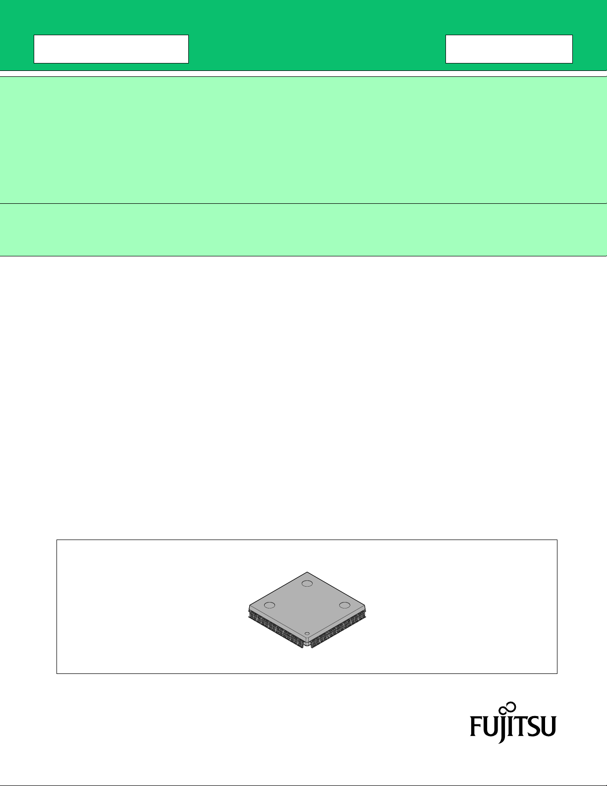
PACKAGE
■■■■
208-pin plastic QFP
(FPT-208P-M04)

MB86291A
(Continued)
• Drawing features:
• Drawing at a peak rate of 800 Mpixels per second (at an internal operating frequency of 100 MHz)
• 2D drawing functions: Point, line, triangle, polygon, BLT, and pattern drawing
• 3D drawing functions: Point, line, and triangle drawing, and hidden surface removal by Z-buffering
• Special effects: Anti-aliasing, bold/dashed-line processing, alpha blending, Gouraud shading, texture
mapping (bilinear filtering, perspective correct) , and tiling
• Display features :
• Maximum display resolution supported : 1024×768 pixels
• Color display either with a color palette of 8 bits per pix el or directly using 5-bit RGB colors of 16 bits per pixel
• Overlaying four layers of screen, of which two lower layers can be divided into the left and right parts
• Supporting two 64×64-pixel hardware cursors
• Output of analog RGB and digital RGB signals
• Capable of superimposing using an external synchronization mode
• Power-supply voltage : Two power supplies at 2.5 V±0.2 V for internal circuits and SDRAM, and 3.3 V±0.2 V
for I/O parts
• Package: Plastic QFP with 208 pins (with a lead pitch of 0.5 mm)
• Process technology : 0.25 µm CMOS
2
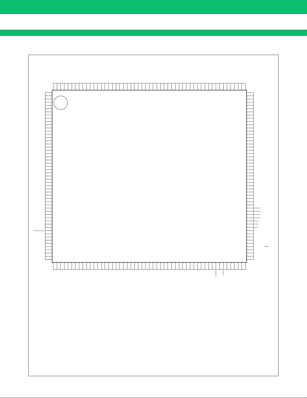
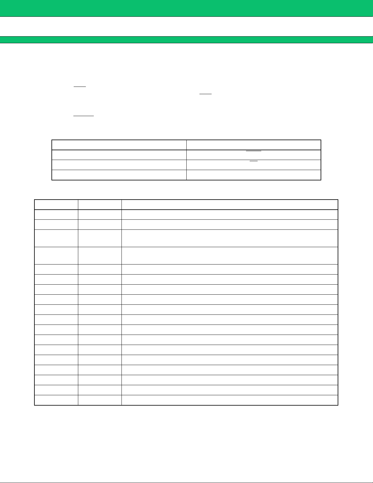
■■■■ PIN ASSIGNMENT
VSS208
HSYNC206
VSYNC205
CSYNC204
VSS203
DCLKO202
VDDE201
VSS
VCC0
VCC1
VSS
VCC2
VDDE
VSS
VCC3
VDDI
VSS
VDDE
VSS
VCC4
VDDI
VSS
VCC5
VDDE
CLKSEL0
CLKSEL1
RESET
MODE0
MODE1
VSS
VCC6
MODE2
TESTL0
VCC7
VSS
R0
R1
R2
R3
R4
R5
R6
R7
G0
G1
G2
G3
G4
G5
G6
G7
B0
B1
B2
B3
B4
B5
B6
B7
GV207
1
2
3
4
5
6
7
8
9
10
11
12
13
14
15
16
17
18
19
20
21
22
23
24
25
26
27
28
29
30
31
32
33
34
35
36
37
38
39
40
41
42
43
44
45
46
47
48
49
50
51
52
VI7200
VI6199
VI5198
VI4197
VI3196
VI2195
VI1194
VI0193
VDDI192
VSS191
DCLKI190
(TOP VIEW)
EO189
RESERVE188
RESERVE187
RESERVE186
RESERVE185
RESERVE184
TESTH5183
CCLK182
VDDE181
VSS180
A24179
A23178
A22
177
A21
176
A20
175
A19
174
A18
173
A17
172
A16
171
VDDI
170
VSS
169
A15
168
A14
167
A13
166
MB86291A
A12
A11
TESTL1
VDDE
161
160
159
VDDI
158
157 VSS
A10
165A9163A8162
164
ACOMPR156
VREF155
VRO154
AVD3153
AOUTR152
AVS3151
AVS2150
AVD2149
AVS1148
AOUTG147
AVD1146
ACOMPG145
AVS0144
AOUTB143
AVD0142
ACOMPB141
VSS140
VDDI139
A7138
A6137
A5136
A4135
A3134
A2133
VDDI132
VSS131
PLLVSS130
S129
OSCOUT128
PLLVDD127
VDDE126
VSS125
CLK124
OSCCNT123
VSS122
VDDI121
WE3120
WE2119
WE1118
WE0117
RD116
BS115
CS114
BCLKI113
VDDI112
VSS111
VDDE110
OPEN109
DTACK/TC108
DRACK/DMAAK107
CKM106
TESTH4105
5355565758596061626364656667686970717273745475777879808182838485868788899091929394
D0D1D2D3D4D5D6
VSS
VDDI
TESTH0
VSS/AVS/PLLVSS
VDDH/VDDE
VDDL/AVD/PLLVDD/VCC/VDDI
AVD
PLLVDD
VCC
OPEN
TESTL0/TESTL1
TESTH0 ~ TESTH5
RESERVE
D7
VSS
VDDE
D8
D9
D10
D11
D12
D13
D14
D15
D17
D18
D19
D16
VSS
VDDI
VDDE
: Ground
: 3.3 V power supply
: 2.5 V power supply
: Analog power supply
: PLL power supply
: Internal DRAM power supply
: Do not connect anything.
: Input the low level.
: Input the high level.
: Input the high level.
D20
D21
D22
D23
D24
VSS
VDDI
D25
D26
Notes : • The AVD and PLLVDD should be separated on the board.
• Insert a bypass capacitor with a superior high-frequency characteristic between the power
supply and ground. Place the capacitor as near the pins as possible.
D27
D28
D29
VSS
VDDE
9576969899
97
D30
D31
RDY
DREQ
INT
100
VSS
101
102
VDDI
TESTH1
103
104
TESTH2
TESTH3
3
MB86291A
PIN DESCRIPTION
■■■■
Host CPU
interface
Clock
D0-D31
A2-A24
BCLKI
RESET
CS
RD
WE0-WE3
RDY
BS
DREQ
DRACK
DTACK
INT
MODE0-
MODE2
TESTL, TESTH
CLK
CKM
CLKSEL0-
CLKSEL1
OSCOUT
OSCCNT
DCLKO
DCLKI
AOUTR, AOUTG,
AOUTB
HSYNC
VSYNC
CSYNC
EO
GV
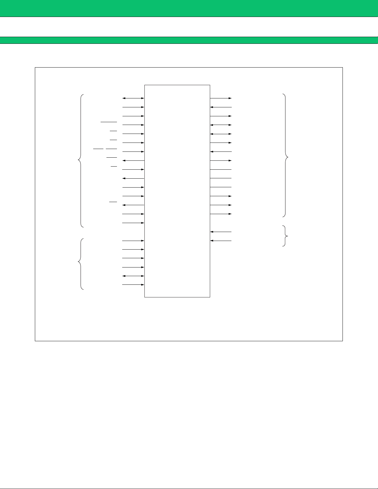
MB86291A
Graphics Controller
HQFP208
S
VREF
VRO
ACOMPR, ACOMPG,
ACOMPB
R0-R7
G0-G7
B0-B7
CCLK
VI0-VI7
Vide output
interface
Vide capture
interface
4
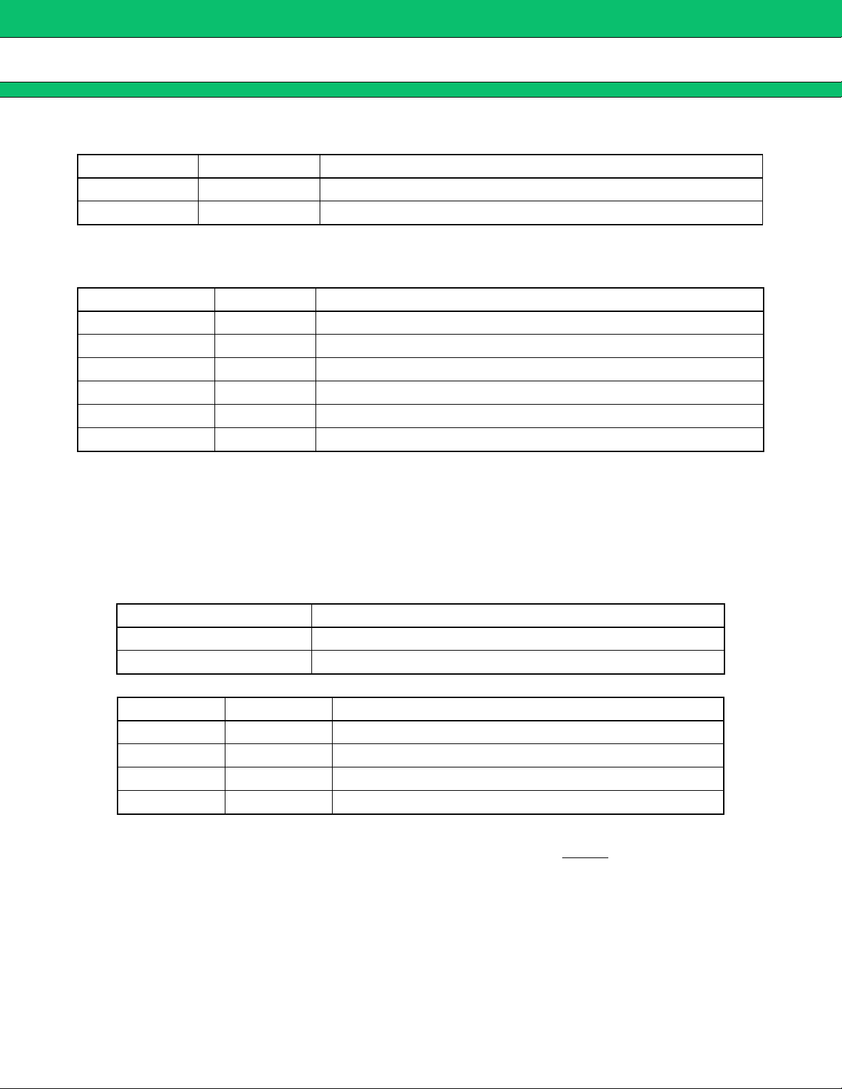
••••
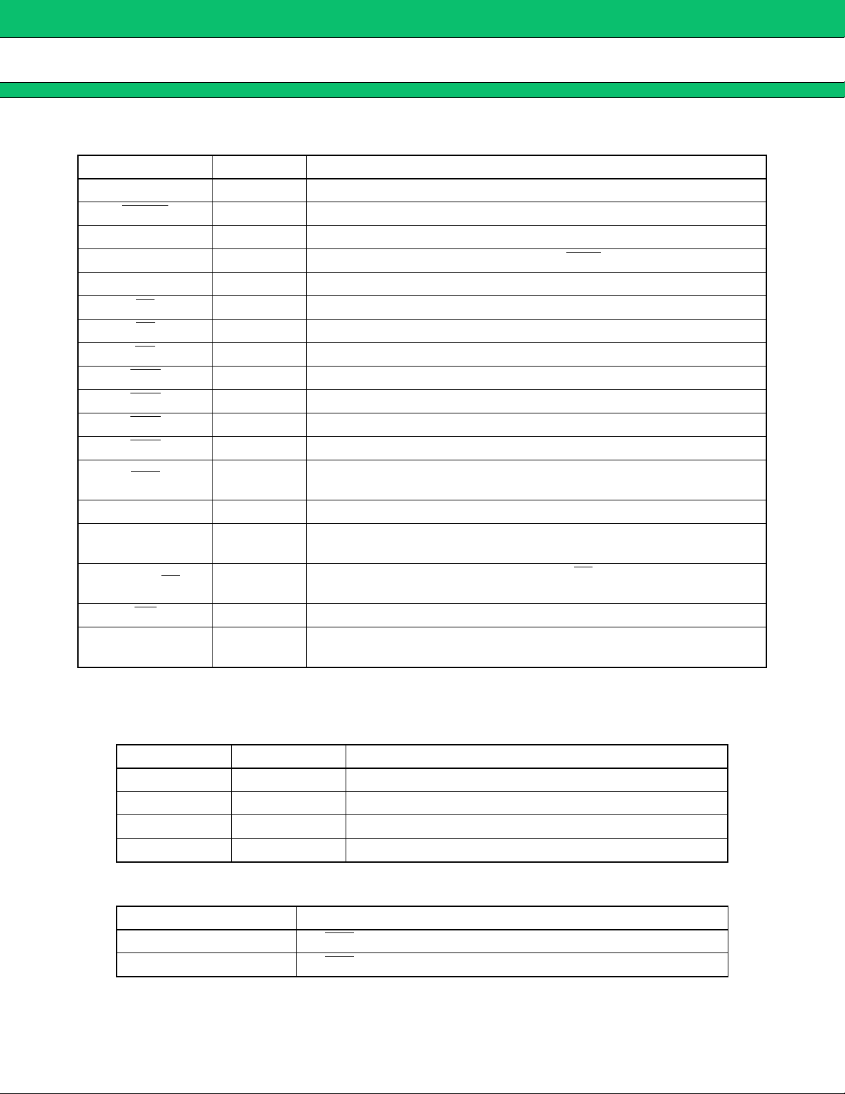
Host Interface Pins
Pin Name Input/output Function
MODE0 to MODE2 Input Host CPU mode/Ready mode select
MB86291A
RESET
D0 to D31 Input/output Host CPU bus data
A2 to A24 Input Host CPU bus address (Connect A[24] to MWR
BCLKI Input Host CPU bus clock
BS
CS
RD Input Read strobe signal
WE0
WE1
WE2 Input D16 to D23 write strobe signal
WE3
RDY
DREQ Output DMA request signal (active low with both SH and V832)
DRACK/DMAAK Input
DTACK/TC
Input Hardware reset
Input Bus cycle start signal
Input Chip select signal
Input D0 to D7 write strobe signal
Input D8 to D15 write strobe signal
Input D24 to D31 write strobe signal
Output
Tristate
Input
Wait request signal
(“0” for wait state with SH3; “1” for wait state with SH4, V832, or SPARClite)
DMA request acknowledge signal (Connect this to DMAAK in V832 mode.
Active high with both SH and V832.)
DMA transfer strobe signal (Connect this to TC in V832 mode. SH = active
high, V832 = active low)
in V832 mode.)
INT
TEST0, TEST1,
TESTH0 to TESTH5
Note : The host interface can connect the MB86291A to the SH4 (SH7750) or SH3 (SH7709) from Hitachi Ltd.
the V832 from NEC, or to the SPARClite (MB86833) from Fujitsu without any external circuit in between.
(Using the SRAM interface allows the MB86291A to use another CPU.) The host CPU is set by the
MODE0 and MODE1 pins as shown below.
MODE1 pin MODE0 pin CPU Type
LLSH3
LHSH4
HLV832
H H SPARClite
Note : The MODE2 pin can be used to set the Ready signal level to be used upon completion of the bus cycle. To
use the MODE2 signal at "H" level, set the software setting to two cycles.
MODE2 pin Ready signal mode
Output Host CPU interrupt signal (SH = active low, V832 = active high)
Input Test signal
L Set RDY
H Set RDY signal to "Ready" level upon completion of bus cycle.
signal to "Not Ready" level upon completion of bus cycle.
5
MB86291A
Notes : • The host interface transfers data signals at a fixed width of 32 bits.
• There are 23 lines for address signals handled in double words ( = 32 bits) and 32 Mbytes of address
space.
• The external bus can be used at an operating frequency of 100 MHz maximum.
• The RDY
sets the wait state in the SH3 mode. Note that the RDY
• The host interface supports DMA transfer using an external DMA controller.
• The host interface generates a host processor interrupt signal.
• The RESET
• Fix the TEST signal at high level.
• In the V832 mode, connect the following pins as specified :
••••
Vide Output Interface
Pin Name Input/output Function
DCLKO Output Display dot clock signal output
DCLKI Input Dot clock signal input
HSYNC Input/output
VSYNC Input/output
CSYNC Output Composite sync signal output
EO Input Even/odd-number field identification input
GV Output Graphics/video select signal
R0-R7 Output Digital video (R) signal output
G0-G7 Output Digital video (G) signal output
B0-B7 Output Digital video (B) signal output
AOUTR Analog output Analog video (R) signal output
AOUTG Analog output Analog video (G) signal output
AOUTB Analog output Analog video (B) signal output
VREF Analog Reference voltage input pin
ACOMPR Analog R-signal compensation pin
ACOMPG Analog G-signal compensation pin
ACOMPB Analog B-signal compensation pin
VRO Analog Reference current setting pin
signal at the low lev el sets the ready state in the SH4 or V832 mode; the signal at the lo w level
signal is a tristate output.
pin requires low lev el input of at least 300 µs after setting “S” (PLL reset signal) to high lev el.
SCARLET Pin Name V832 Signal Name
A24 MWR
DTACK TC
DRACK DMAAK
Horizontal sync signal output
Horizontal sync signal input in external synchronization mode
Vertical sync signal output
Vertical sync signal input in external synchronization mode
Notes : • The video output interface contains an 8-bit D/A converter to output analog RGB signals. Also, the
eight-bit RGB digital output pins can connect an external digital video encoder.
• Using an additional external circuit, the video output interface can generate composite video signals.
• The video output interface can provide display synchronized with external video. The mode for
synchronization with the DCLKI signal can be selected as well as the mode for synchronization with a set
dot clock as for normal display.
6

MB86291A
• The HSYNC and VSYNC signals must be pulled up outside the LSI as they enter the input state upon reset.
• Terminate the AOUTR, AOUTG, and AOUTB pins with a resistance of 75 Ω.
• Input 1.1 V to the VREF pin. Between this pin and analog ground, insert a bypass capacitor (one with a
superior high-frequency characteristic such as a laminated ceramic capacitor).
• Connect the ACOMPR, A COMPG, and ACOMPB pins to the 0.1 µF ceramic capacitor ahead of the analog
power supply.
• Connect the VRO pin to the analog ground with a 2.7 kΩ resistor.
• For noninterlaced display in external synchronization mode, input "0" to the EO pin, for example, using
a pull-down resistor.
• The GV signal serves to switch between graphics and video for chroma keying. The pin outputs a low
level signal to select video.
7
MB86291A
••••
Video Capture Interface
Pin Name Input/output Function
CCLK Input Digital video input clock signal input
VI0-VI7 Input Digital video data input
Note : The video capture interface inputs digital video signals in the ITU-RBT-656 format.
••••
Clock Input
Pin Name Input/output Function
CLK Input Clock input signal
S Input PLL reset signal
CKM Input Clock mode signal
CLKSEL1, CLKSEL0 Input Clock rate select signal
OSCOUT*
OSCCNT*
1
2
Input/output For connection of crystal oscillator (Reserved)
Input For selection of crystal oscillator (Reserved)
*1 : Do not connect anything.
*2 : Input the “H” level.
Notes : • The clock input bloc k inputs the clock signal that serves as the basis f or the reference clock f or the internal
operating clock and displa y dot clock. Usually input 4 Fsc ( = 14.31818 MHz) . The internal PLL generates
the internal operating clock signal of 100 MHz and the display reference clock signal of 200 MHz.
• The internal operating clock signal to be used can be selected between the clock signal (100 MHz)
generated by the internal PLL and the bus clock BCLKI input to the host CPU interf ace. Select the BCLKI
input to use the host CPU bus at 100 MHz.
CKM Clock Mode
L Select internal PLL output.
H Select host CPU bus clock (BCLKI)
Note : Use the CLKSEL pin to select the input clock frequency for using the internal PLL with CKM = L.
CLKSEL1 CLKSEL0 Clock Frequency
L L Input 13.5 MHz.
L H Input 14.32 MHz.
H L Input 17.73 MHz.
HHReserved
Note : Immediately after turning the power supply on, input a pulse whose low lev el period is 500 ns or more to the
S pin before setting it to high le v el. After the S signal goes high, input the RESET
µs or more
signal at low level for 300
8

BLOCK DIAGRAM
■■■■
MB86291A
D0-D31
A2-A24
Host
Interface
Memory
Interface
Controller
Embedded SDRAM
External Video
Interface Controller
Display Controller
DAC
Geometry
Engine
2D/3D
Rendering
Engine
RBT656
DRGB
ARGB
9

MB86291A
FUNCTION BLOCKS
■■■■
••••
Host Interfacee
This block allo ws the MB86291A to be connected to the SH3 or SH4 microprocessor from Hitachi Ltd., the V83x
microprocessor from NEC, or to the SPARCLite from Fujitsu without any external circuit in between. The b lock
provides an interface to transfer display list and texture pattern data directly from main memory to this device’s
graphics memory or internal register using the external DMA controller.
••••
Memory Interface Controller and Embedded SDRAM
The embedded 16-megabit SDRAM eliminates the need for e xternal memory . The SDRAM operates at 100 MHz.
••••
Display Controller
This block contains a three-channel, eight-bit D-A con verter to output analog RGB signals. The bloc k has eightbit RGB digital video outputs, allowing an external digital video encoder to be connected. The block supports
resolutions of up to XGA (1024×768 pixels), enabling flexible setting.
••••
External Video Interface Controller
This block can input digital video in the ITU RBT-656 format by connecting an external digital video decoder
using the eight-bit video input pin. Input video data is stored temporarily in graphics memory and then displayed
on the screen in synchronization with the display scan.
The block supports video in the NTSC and PAL formats.
••••
Set-up Engine
The on-chip geometry engine executes mathematical operations required f or graphics processing precisely using
the fronting-point format. The geometry engine executes the required geometry processes selected depending
on the drawing mode and primitive type settings up to the final drawing process.
••••
2D/3D Rendering Engine
This block draws images in two or three dimensions.
•2D drawing
The block provides the anti-aliasing and alpha blending functions to display high-quality images even on a lo w-
resolution LCD.
•3D drawing
The block provides true 3D drawing functions such as perspective texture mapping and Gouraud shading.
10
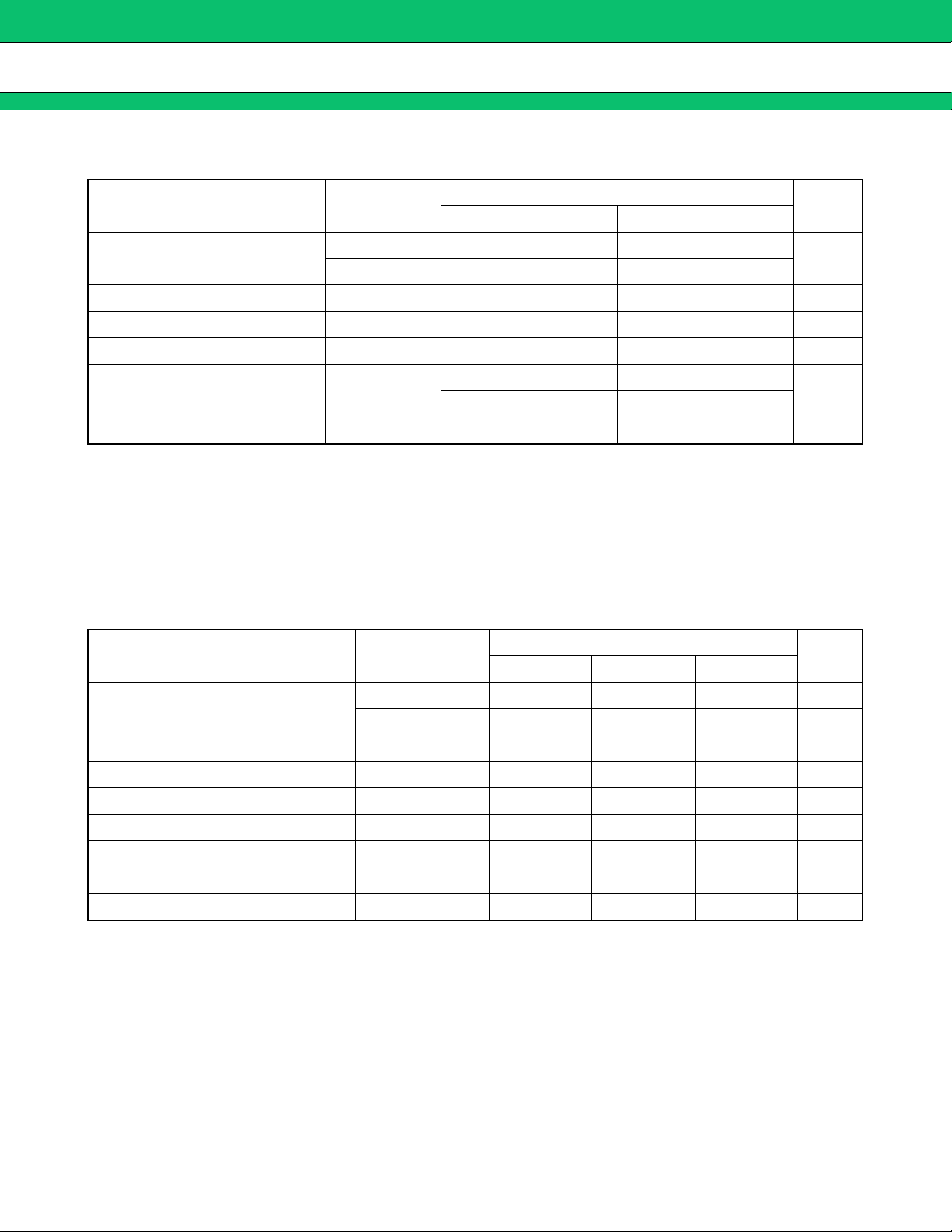
ABSOLUTE MAXIMUM RATINGS
■■■■
MB86291A
Parameter Symbol
Unit
Min Max
Rating
1
V
DDL*
− 0.5 + 3.0
Power supply voltage
V
DDH − 0.5 + 4.0
Input voltage V
I − 0.5 VDDH + 0.5 (< 4.0) V
Output current IO − 13 + 13 mA
Power pin current I
POW 60 mA
0 + 70
Ambient operating temperature T
A
− 30*
2
+ 85*
2
°C
Ambient storage temperature Tstg − 55 + 125 °C
*1 : The analog and PLL power supplies are included.
*2 : Model supporting a wider range of temperatures
WARNING: Semiconductor devices can be permanently damaged by application of stress (voltage, current,
temperature, etc.) in excess of absolute maximum ratings. Do not exceed these ratings.
RECOMMENDED OPERATING CONDITION
■■■■
Value
Parameter Symbol
Unit
Min Typ Max
1
V
DDL*
2.3 2.5 2.7 V
Power supply voltage
VDDH 3.0 3.3 3.6 V
V
Input voltage (High level) V
Input voltage (Low level) V
IH 2.0 VDDH + 0.3 V
IL − 0.3 + 0.8 V
VREF pin input voltage VREF 1.05 1.10 1.15 V
VRO pin external resistor R
AOUT pin external resistor*
ACOMP pin external capacitor*
2
3
Ambient operating temperature T
VRO 2.7 kΩ
RAOUT 75 Ω
CACOMP 0.1 µF
A − 40 + 85 °C
*1 : The analog and PLL power supplies are included.
*2 : AOUTR, AOUTG and AOUTB pins
*3 : ACOMPR, ACOMPG, and ACOMPB pins
11

MB86291A
Notes : • The VDDL and VDDH power supplies can be turned on or off in either order.
Note, however, that the VDDH voltage must not be applied alone continuously for several seconds.
• After turning the power on, input a pulse remaining at low lev el f or at least 500 ns to the S pin. Then, set
the S pin to high level and input the RESET
WARNING: The recommended operating conditions are required in order to ensure the normal operation of the
semiconductor device. All of the device’s electrical characteristics are warranted when the device is
operated within these ranges.
Always use semiconductor devices within their recommended operating condition ranges. Operation
outside these ranges may adversely affect reliability and could result in device failure.
No warranty is made with respect to uses, operating conditions, or combinations not represented on
the data sheet. Users considering application outside the listed conditions are advised to contact their
FUJITSU representatives beforehand.
signal held at low level for at least 300 µs.
12

ELECTRICAL CHARACTERISTICS
■■■■
1. DC Characteristics
Parameter Symbol
Output voltage (High level) *
Output voltage (Low level) *
Output current (High level)
Output current (Low level)
1
2
MB86291A
VDDL = 2.5 V ± 0.2 V, VDDH = 3.3 V ± 0.3, VSS = 0.0 V, TA = 0 °C to + 70 °C
Value
Min Typ Max
VOH VDDH − 0.2 VDDH V
VOL 0.0 0.2 V
IOHM*
I
OHH*
OLM*
I
IOLH*
4
3
4
3
− 4.0
mA
− 8.0
4.0
mA
8.0
Unit
AOUT output current*
5
Full scale
I
AOUT
9.90 10.42 10.94 mA
Zero scale 0 2 20 µA
AOUT voltage*
Input leakage current I
6
VAOUT − 0.1 + 1.1 V
L ± 5 µA
Pin capacitance C 16 pF
*1 : Value when −100 µA current flows into output pins.
*2 : Value when 100 µA current flows into output pins.
*3 : Output characteristics of INT
, DREQ, and RDY
*4 : Output characteristics of the signals (excluding analog signals) other than those in *3
*5 : AOUTR, AOUTG, and AOUTB pin output current. Condition V
(The full-scale output current calculation expression is (V
REF = 1.10 V, RVRO = 2.7 kΩ
REF / RVRO) × 25.575)
*6 : AOUTR, AOUTG, and AOUTB pins
13

MB86291A
2. AC Characteristics
• Input measurement conditions
(VIH = 2.0 V, VIL = 0.8 V)
r
t
IH
V
Input
VIL
80%
20%
•tr, tf ≤ 5 ns
•Input measurement standard : (VIH + VIL) / 2
• Output measurement conditions
VIH
Input
VIL
VOH
t
pHL,
t
pZL
(VIH + VIL) / 2
IH + VIL) /2
(V
tf
80%
20%
tpLH,
t
pZH
14
Output 1
VOL
Output 2
VOL
VOH
Output 3
•Output measurement standard : t
pLZ : VOL + 0.5 V
t
pHZ : VOH − 0.5 V
Else : V
DD/2
VDD/2
tpHZ
tpLZ
V
DD/2
0.5 V
0.5 V
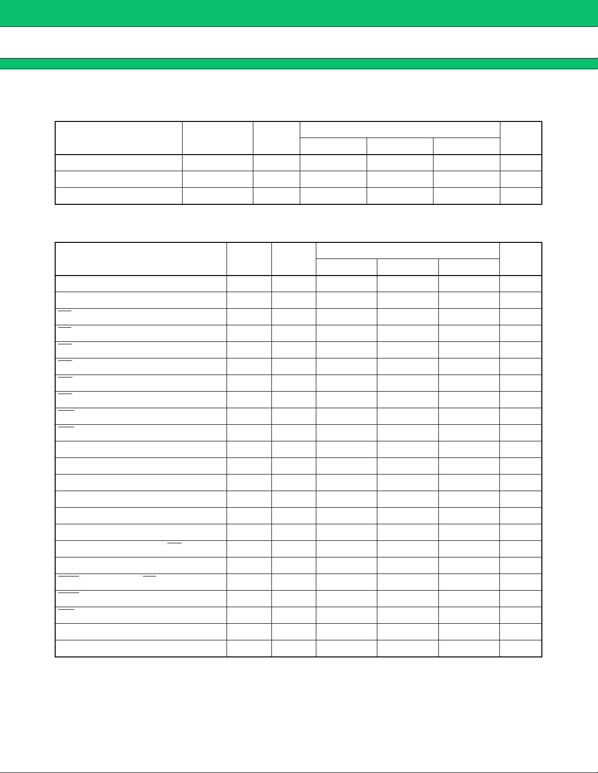
(1) Host Interface
Clock signals
••••
Parameter Symbol
Condi-
tion
MB86291A
Value
Unit
Min Typ Max
BCLKI frequency f
BCLKI H period t
BCLKI L period t
Host interface signals
••••
BCLKI 100 MHz
HBCLKI 1 ns
LBCLKI 1 ns
(External load of 20 pF)
Parameter Symbol
Address setup time t
Condi-
tion
ADS 4 ns
Min Typ Max
Value
Unit
Address hold time tADH 0 ns
BS
setup time tBSS 3 ns
BS
hold time tBSH 0 ns
CS setup time tCSS 3 ns
CS
hold time tCSH 0 ns
RD
setup time tRDS 3 ns
RD hold time tRDH 0 ns
WE
setup time tWES 5 ns
WE
hold time tWEH 1 ns
Write data setup time t
WDS 3 ns
Write data hold time tWDH 0 ns
DTACK setup time t
DTACK hold time t
DAKS 3 ns
DAKH 0 ns
DRACK setup time tDRKS 3 ns
DRACK hold time t
Read data delay time (to RD
) tRDDZ 3.0 11.0 ns
DRKH 0 ns
Read data delay time tRDD *2 4.5 10.5 ns
RDY
delay time (to CS) tRDYDZ 2.5 5.0 ns
RDY
delay time tRDYD 2.5 6.0 ns
INT delay time tINTD 3.0 6.5 ns
DREQ delay time t
MODE hold time t
DRQD 2.5 6.0 ns
MODH *1 20.0 ns
*1 : Hold time for reset cancellation
*2 : Read data is output one cycle before the CPU samples it.
15

MB86291A
•••• Clock
BCLKI
•••• Input setup and hold times
BCLKI
1/fBCLKI
tHBCLKI tLBCLKI
A2~A24,
BS, CS,
DTACK,
DRACK
•••• Read/write enable (RD
BCLKI
BS
RD, WE
tADS, tBSS, tCSS,
t
DAKS, tDRKS
, WE) and input data (D) setup times
tRDS, tWES
tADH, tBSH, tCSH,
t
DAKH, tDRKH
tRDH,
tWEH
16
D0~D31
tWDS
tWDH

•••• DREQ output delay time
BCLKI
DREQ (output)
INT
output delay time
••••
MB86291A
tDRQD
BCLKI
INT (output)
RDY
••••
delay value (with respect to CS)
BCLKI
CS
tINTD
RDY (output)
High-Z High-Z
tRDYDZ tRDYDZ
17

MB86291A
•••• RDY/D output delay values
BCLKI
RD
D0~D31
(output)
RDY
•••• MODE signal hold time
RESET
tRDD
tRDYD
Output data
tRDYD
tRDDZ
High-Z
18
MODE0~
MODE2
tMODH
(2) Video Interface
Clock
••••
Parameter Symbol
Condi-
tion
MB86291A
Value
unit
Min Typ Max
CLK frequency f
CLK H period t
CLK L period t
CLK 14.32 MHz
HCLK 25 ns
LCLK 25 ns
DCLKI frequency fDCLKI 67 MHz
DCLKI H period t
DCLKI L period t
HDCLKI 5 ns
LDCLKI 5 ns
DCLKO frequency fDCLKO 67 MHz
•••• Input signals
Parameter Symbol
t
WHSYNC0 *1 3 clock
Condi-
tion
Min Typ Max
Value
unit
HSYNC input pulse width
t
WHSYNC1 *2 3 clock
HSYNC input setup time t
SHSYNC *2 10 ns
HSYNC input hold time tHHSYNC *2 10 ns
VSYNC input pulse width t
WHSYNC1 1
EO input setup time t
SEO *3 10 ns
HSYNC
1 cycle
EO input hold time t
HEO *3 10 ns
*1 : Applied only in PLL synchronization mode (CKS = 0) . The reference clock is the internal PLL’s output with Cycle
= 1/ (14 f
CLK) .
*2 : Applied only in DCLKI synchronization mode (CKS = 1) . The reference clock is DCLKI.
*3 : Based on the edge with VSYNC negated.
Output signals
••••
Parameter Symbol
EO output delay time t
Condi-
tion
DEO *1.5 11 ns
Min Typ Max
Value
unit
HSYNC output delay time tDHSYNC 1.5 11 ns
VSYNC output delay time t
CSYNC output delay time t
GV output delay time t
DVSYNC 1.5 11 ns
DCSYNC 1.5 11 ns
DGV 1.5 11 ns
* : The EO output varies at the same time as VSYNC is asserted.
19

MB86291A
•••• Clock
1/fCLK
CLK
HSYNC signal setup and hold
••••
DCLKI
HSYNC
(input)
•••• EO signal setup and hold
tHCLK
tHDCLKI
tLCLK
VIH
VIL
1/fDCLKI
tLDCLKI
tSHSYNC tHHSYNC
VSYNC
EO
(input)
Output signal delay
••••
DCLKO
EO (output)
HSYNC (output)
VSYNC (output)
CSYNC
GV
tSEO
tHEO
tDEO, tDHSYNC, tDVSYNC,
t
DCSYNC, tDGV
20

(3) Video Capture Interface
Clock
••••
Parameter Symbol
Condi-
tion
MB86291A
Value
unit
Min Typ Max
CCLKI frequency f
CCLKI H period t
CCLKI L period t
HCCLKI 1 ns
LCCLKI 1 ns
•••• Input signals
Parameter Symbol
VI setup time (External load of 25 pF) t
VI hold time (External load of 15 pF) t
Clock
••••
tHCLK tLCLK
CLK
VIH
CCLKI 27 MHz
Condi-
tion
VIS 11 ns
VIH 2 ns
1/fCLK
VIL
Min Typ Max
Value
unit
•••• Video input
CCLKI
VI0~VI7
tVIS tVIH
21

MB86291A
(4) PLL Standards
Parameter
Min Typ Max
Input frequency 14.31818 MHz
Output frequency 200.45452 MHz Multiplied by 14
Duty ratio 93.1 101.3 % PLL output clock H/L pulse width ratio
Jitter − 150 + 180 ps
Value
Unit Remarks
Cycle difference between two
consecutive cycles
22

ORDERING INFORMATION
■■■■
Part Number Package Remarks
MB86291APFVS
MB86291A
208-pin plastic QFP
(FPT-208P-M04)
23

MB86291A
PACKAGE DIMENSION
■■■■
208-pin plastic QFP
(FPT-208P-M04)
30.60±0.20(1.205±.008)SQ
28.00±0.10(1.102±.004)SQ
157
INDEX
208
LEAD No.
1
0.50(.020)
0.22±0.05
(.009±.002)
Note : Pins width and pins thickness include plating thickness.
+0.03
–0.08
0.17
"A"
+.001
.007 –.003
0.08(.003)
Details of "A" part
+0.20
–0.30
3.75
+.008
.148 –.012
0°~8°
0.50±0.20
(.020±.008)
0.60±0.15
(.024±.006)
(Mounting height)
0.25(.010)
0.40
.016
(Stand off)
105156
52
0.08(.003)
104
53
M
+0.10
–0.15
+.004
–.006
C
2000 FUJITSU LIMITED F208020S-c-2-3
Dimension in mm (inches)
24

MB86291A
FUJITSU LIMITED
For further information please contact:
Japan
FUJITSU LIMITED
Marketing Division
Electronic Devices
Shinjuku Dai-Ichi Seimei Bldg. 7-1,
Nishishinjuku 2-chome, Shinjuku-ku,
Tokyo 163-0721, Japan
Tel: +81-3-5322-3353
Fax: +81-3-5322-3386
http://edevice.fujitsu.com/
North and South America
FUJITSU MICROELECTRONICS AMERICA, INC.
3545 North First Street,
San Jose, CA 95134-1804, U.S.A.
Tel: +1-408-922-9000
Fax: +1-408-922-9179
Customer Response Center
Mon. - Fri.: 7 am - 5 pm (PST)
Tel: +1-800-866-8608
Fax: +1-408-922-9179
http://www.fma.fujitsu.com/
Europe
FUJITSU MICROELECTRONICS EUR OPE GmbH
Am Siebenstein 6-10,
D-63303 Dreieich-Buchschlag,
Germany
Tel: +49-6103-690-0
Fax: +49-6103-690-122
http://www.fme.fujitsu.com/
Asia Pacific
FUJITSU MICROELECTRONICS ASIA PTE. LTD.
#05-08, 151 Lorong Chuan,
New Tech Park,
Singapore 556741
Tel: +65-281-0770
Fax: +65-281-0220
http://www.fmal.fujitsu.com/
Korea
FUJITSU MICROELECTRONICS K OREA LTD.
1702 KOSMO TOWER, 1002 Daechi-Dong,
Kangnam-Gu,Seoul 135-280
Korea
Tel: +82-2-3484-7100
Fax: +82-2-3484-7111
All Rights Reserved.
The contents of this document are subject to change without notice.
Customers are advised to consult with FUJITSU sales
representatives before ordering.
The information and circuit diagrams in this document are
presented as examples of semiconductor device applications, and
are not intended to be incorporated in devices for actual use. Also,
FUJITSU is unable to assume responsibility for infringement of
any patent rights or other rights of third parties arising from the use
of this information or circuit diagrams.
The products described in this document are designed, developed
and manufactured as contemplated for general use, including
without limitation, ordinary industrial use, general office use,
personal use, and household use, but are not designed, developed
and manufactured as contemplated (1) for use accompanying fatal
risks or dangers that, unless extremely high safety is secured, could
have a serious effect to the public, and could lead directly to death,
personal injury, severe physical damage or other loss (i.e., nuclear
reaction control in nuclear facility, aircraft flight control, air traffic
control, mass transport control, medical life support system, missile
launch control in weapon system), or (2) for use requiring
extremely high reliability (i.e., submersible repeater and artificial
satellite).
Please note that Fujitsu will not be liable against you and/or any
third party for any claims or damages arising in connection with
above-mentioned uses of the products.
Any semiconductor devices have an inherent chance of failure. You
must protect against injury, damage or loss from such failures by
incorporating safety design measures into your facility and
equipment such as redundancy, fire protection, and prevention of
over-current levels and other abnormal operating conditions.
If any products described in this document represent goods or
technologies subject to certain restrictions on export under the
Foreign Exchange and Foreign Trade Law of Japan, the prior
authorization by Japanese government will be required for export
of those products from Japan.
F0203
FUJITSU LIMITED Printed in Japan
 Loading...