


FUJITSU SEMICONDUCTOR
DATA SHEET
Memory FRAM
CMOS
256 K (32 K × 8) Bit SPI
MB85RS256
■ DESCRIPTION
MB85RS256 is a FRAM (Ferroelectric Random Access Memory) chip in a configuration of 32,768 words × 8 bits,
using the ferroelectric process and silicon gate CMOS process technologies for forming the nonvolatile memory
cells.
MB85RS256 adopts the Serial Peripheral Interface (SPI).
Unlike SRAM, MB85RS256 is able to retain data without back-up battery.
The memory cells used for the MB85RS256 has improved at least 10
outperforming Flash memory and E
MB85RS256 does not take long time to write data unlike Flash memories nor E
no wait time.
2
PROM in the number.
DS05-13105-2E
10
times of read/write operation significantly
2
PROM, and MB85RS256 takes
■ FEATURES
• Bit configuration : 32,768 × 8 bits
• Operating power supply voltage : 3.0 V to 3.6 V
• Operating frequency : 15 MHz (Max)
• Serial Peripheral Interface : SPI (Serial Peripheral Interface)
Correspondent to SPI mode 0 (0, 0) and mode 3 (1, 1)
• Operating temperature range : −20 °C to +85 °C
• Data retention : 10 years (+55 °C)
• High endurance 10 Billion Read/writes (Min)
• Package : 8-pin plastic SOP (FPT-8P-M02)
Copyright©2005-2007 FUJITSU LIMITED All rights reserved
MB85RS256
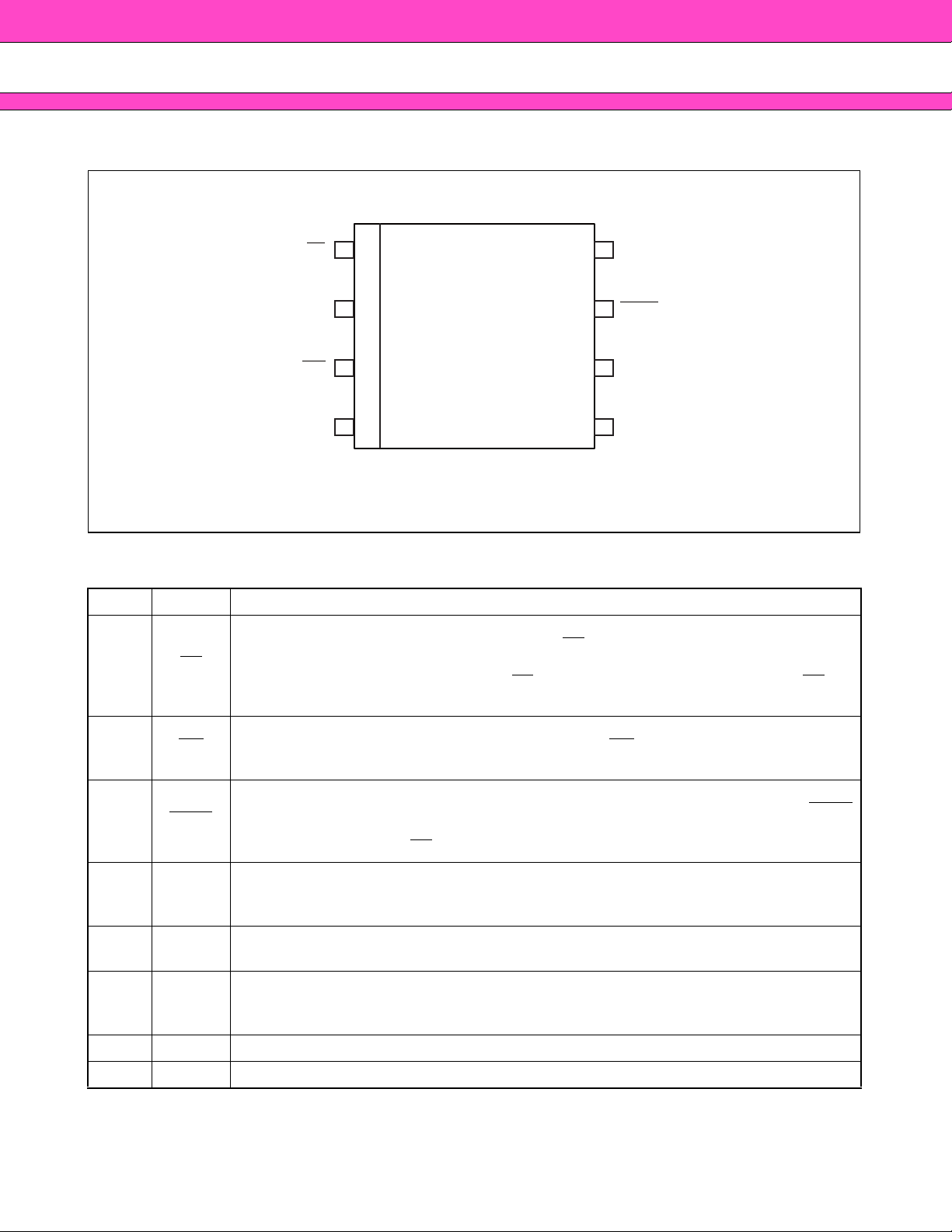
■ PIN ASSIGNMENT
(TOP VIEW)
CS
SO
WP
VSS SI
1
2
3
(FPT-8P-M02)
8
7
6
54
■ PIN FUNCTIONAL DESCRIPTIONS
Pin No. Pin Name Functional description
Chip Select
This is an input pin to make chips select. When CS
1CS
status as long as device is not write status internally, and SO becomes High-Z. Other inputs
from pins are ignored for this time. When CS
to be “L” before inputting op-code.
is “L”, device is in select (active) status. CS has
is “H”, device is in deselect (standby)
VDD
HOLD
SCK
Write Protect
3WP
7HOLD
6SCK
5SI
2SO
8 VDD Supply Voltage
4 VSS Ground
2
This is a pin to control writing to a status register. When WP
is not operated.
Hold
This pin is used to interrupt serial input/output without making chips deselect. When HOLD
is “L”, hold operation is activated, SO becomes High-Z, SCK and SI become don’t care.
While the hold operation, CS
Serial Clock
This is a clock input pin to input/output serial data. SI is loaded synchronously to a rising
edge, SO is output synchronously to a falling edge.
Serial Data Input
This is an input pin of serial data. This inputs op-code, address, and writing data.
Serial Data Output
This is an output pin of serial data. Reading data of FRAM memory cell array and status
register data are output. This is High-Z during standby.
is “L”, writing to a status register
has to be retained “L”.
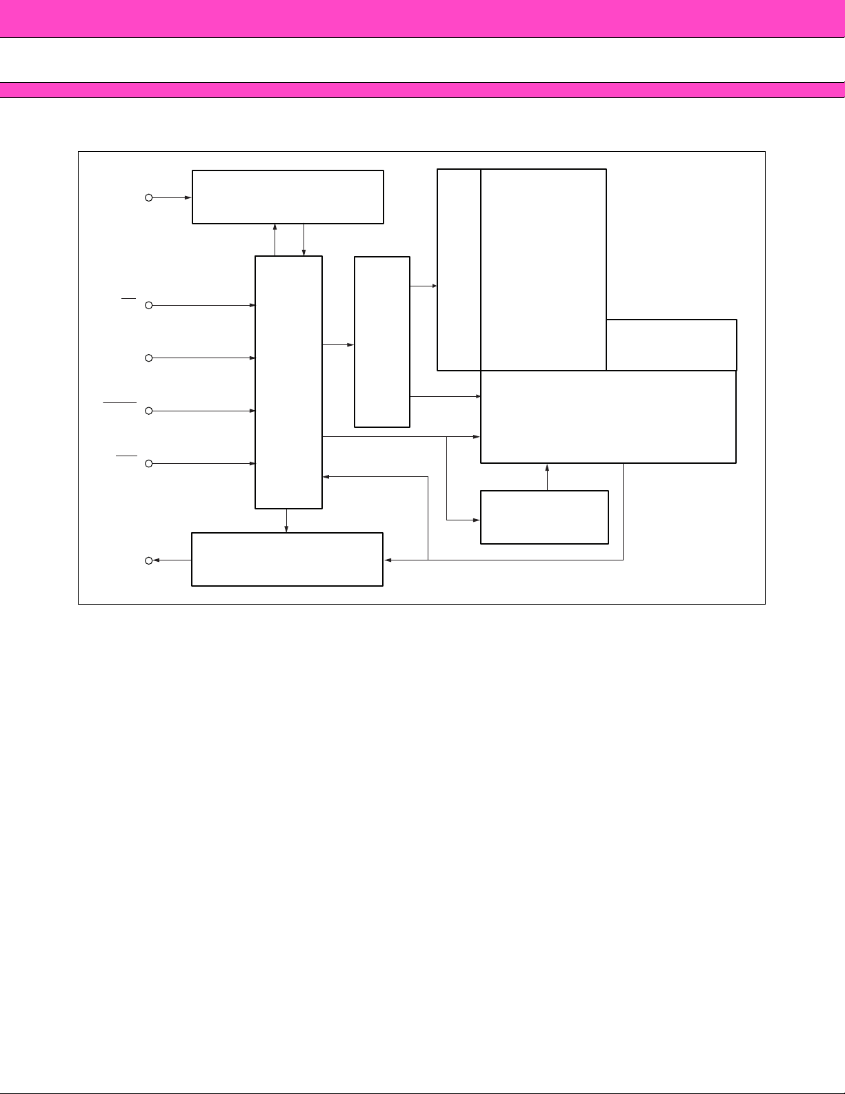
■ BLOCK DIAGRAM
MB85RS256
SI
CS
SCK
HOLD
WP
SO
Serial-Parallel Converter
Control Circuit
Parallel-Serial Converter
FRAM Cell Array
32,768 ✕ 8
Row-Decoder
FRAM
Status Register
Address Counter
Column Decoder/Sense Amp/
Write Amp
Data Register
3
MB85RS256
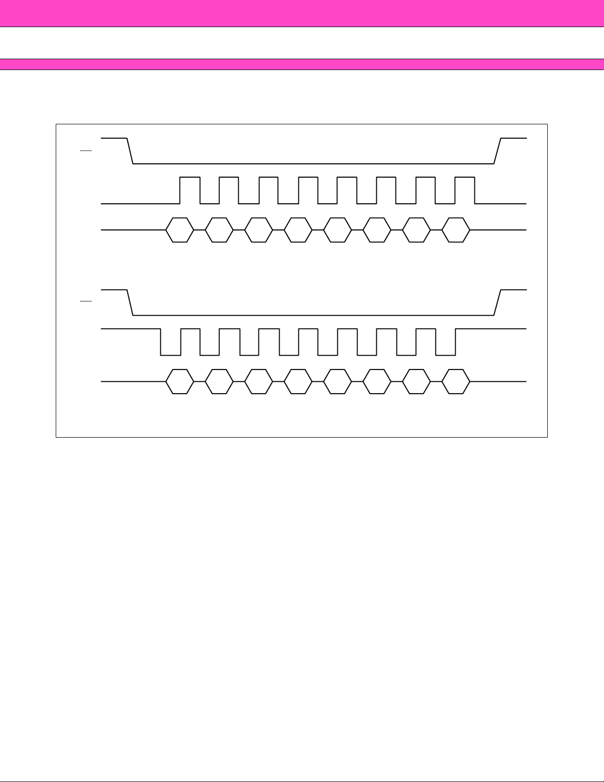
■ SPI MODE
MB85RS256 is corresponding to the SPI mode 0 (CPOL = 0, CPHA = 0) , and SPI mode 3 (CPOL = 1, CPHA = 1) .
CS
SCK
CS
SCK
SI
SI
76543 210
MSBLSB
76543 210
MSBLSB
SPI Mode 0
SPI Mode 3
4
MB85RS256
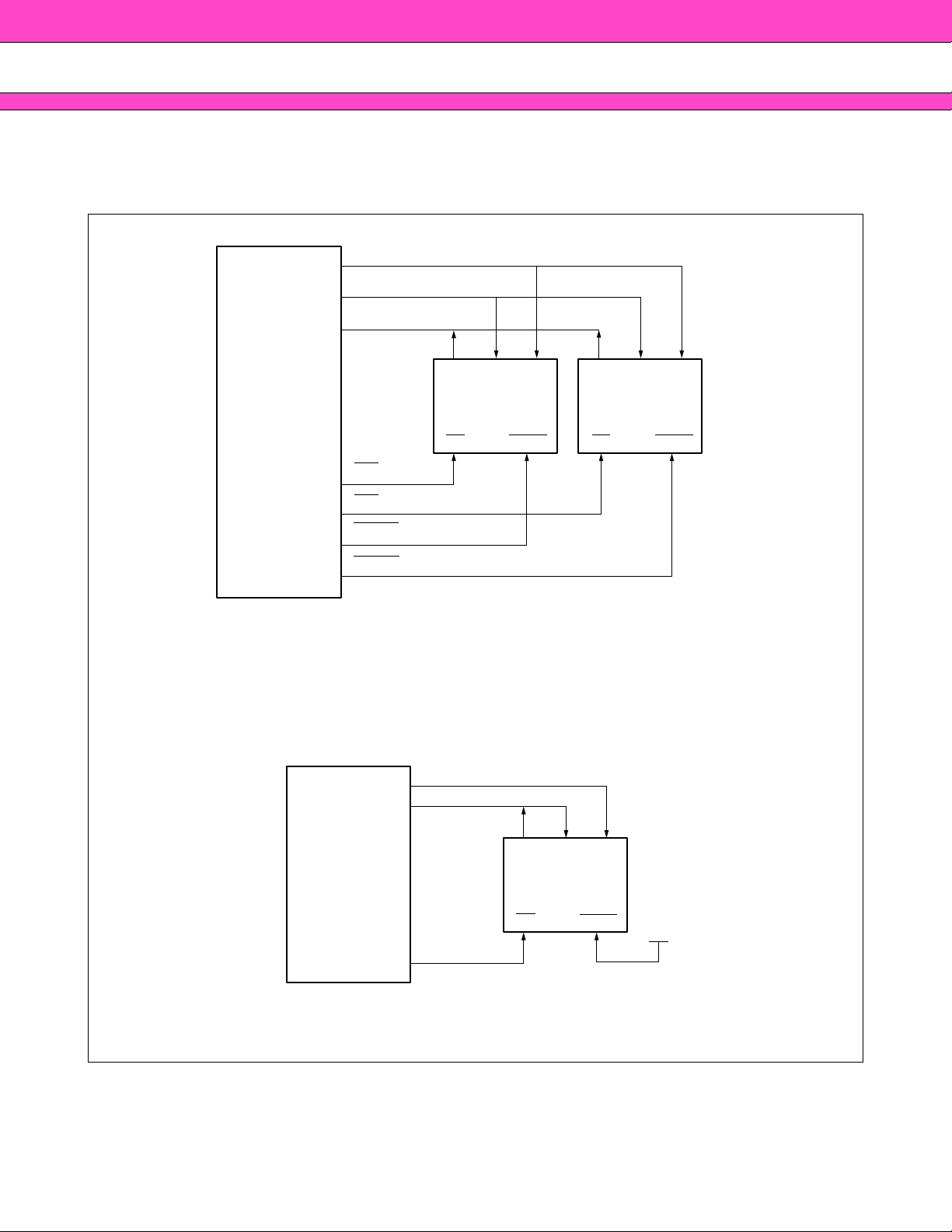
■ SERIAL PERIPHERAL INTERFACE (SPI)
MB85RS256 works as a slave of SPI. More than 2 devices can be connected by using microcontroller equipped
with SPI port. By using a microcontroller not equipped with SPI port, SI and SO can be bus connected to use.
SCK
MOSI
MISO
SISO
SCK
SPI
Microcontroller
SCK
SISO
MB85RS256 MB85RS256
CS
SS1
SS2
HOLD1
HOLD2
HOLD
System Configuration with SPI Port
Microcontroller
CS
SCK
SISO
MB85RS256
HOLD
MOSI : Master Out Slave In
MISO : Master In Slave Out
SS : Slave Select
CS
HOLD
System Configuration without SPI Port
5
MB85RS256
■ STATUS REGISTER
Bit No. Bit Name Function
Status Register Write Protect
This is a bit composed of nonvolatile memories (FRAM). WPEN is related
7 WPEN
6 to 4 ⎯
to WP
input to protect writing to a status register (refer to “■ WRITING
PROTECT”). Writing with the WRSR command and reading with the
RDSR command are possible.
Not Used Bits
These are bits composed of nonvolatile memories, writing with the WRSR
command is possible, and “000” is written before shipment. These bits are
not used but they are read with the RDSR command.
3BP1
2BP0
1WEL
0 0 This is a bit fixed to “0”.
Block Protect
This is a bit composed of nonvolatile memory (FRAM). This defines block
size for writing protect with the WRITE command (refer to “■ BLOCK
PROTECT”). Writing with the WRSR command and reading with the
RDSR command are possible.
Write Enable Latch
This indicates FRAM memory and status register are writable. The WREN
command is for setting, and the WRDI command is for resetting. With the
RDSR command, reading is possible but writing is not possible with the
WRSR command. WEL is reset after the following operations.
The time when power is up.
The time when the WRDI command is input.
The time when the WRSR command is input.
The time when the WRITE command is input.
■ OP-CODE
MB85RS256 accepts 6 kinds of command specified in op-code. Op-code is a code composed of 8 bits shown
in the table below. When invalid codes other than codes below are input, they are ignored. If CS
inputting op-code, the command are not performed.
Name Description Op-code
is risen while
WREN Set Write Enable Latch 0000 0110
WRDI Reset Write Enable Latch 0000 0100B
RDSR Read Status Register 0000 0101B
WRSR Write Status Register 0000 0001B
READ Read Memory Code 0000 0011B
WRITE Write Memory Code 0000 0010B
6
B

MB85RS256
■ COMMAND
• WREN
The WREN command sets WEL (Write Enable Latch) . WEL has to be set with the WREN command before
writing operation (WRSR command and WRITE command) .
CS
76543210
SCK
SI
SO
00000110
High-Z
InvalidInvalid
• WRDI
The WRDI command resets WEL (Write Enable Latch) . Writing operation (WRITE command and WRSR
command) are not performed when WEL is reset.
CS
76543210
SCK
SI
SO
00000100
High-Z
InvalidInvalid
7

MB85RS256
• RDSR
The RDSR command reads status register data. After op-code of RDSR is input to SI, 8-cycle clock is input to
SCK. The SI value is invalid for this time. SO is output synchronously to a falling edge of SCK. Continuously
reading status register is enabled by keep on sending SCK before rising CS
CS
with the RDSR command.
SCK
SI
SO
76543210
00000101
High-Z
Invalid
Data Out
MSB
76543210
Invalid
LSB
• WRSR
The WRSR command writes data to the nonvolatile memory bit of status register. After performing WRSR opcode to a SI pin, 8 bits writing data is input. WEL (Write Enable Latch) is not able to be written with WRSR
command. a SI value correspondent to bit 1 is ignored. Bit 0 of the status register is fixed to “0” and cannot be
written. The SI value corresponding to bit 0 is ignored.
CS
SCK
SI
SO
76543210
Instruction
00000001
MSB
High-Z
Data In
76543210
76543210
LSB
8
MB85RS256
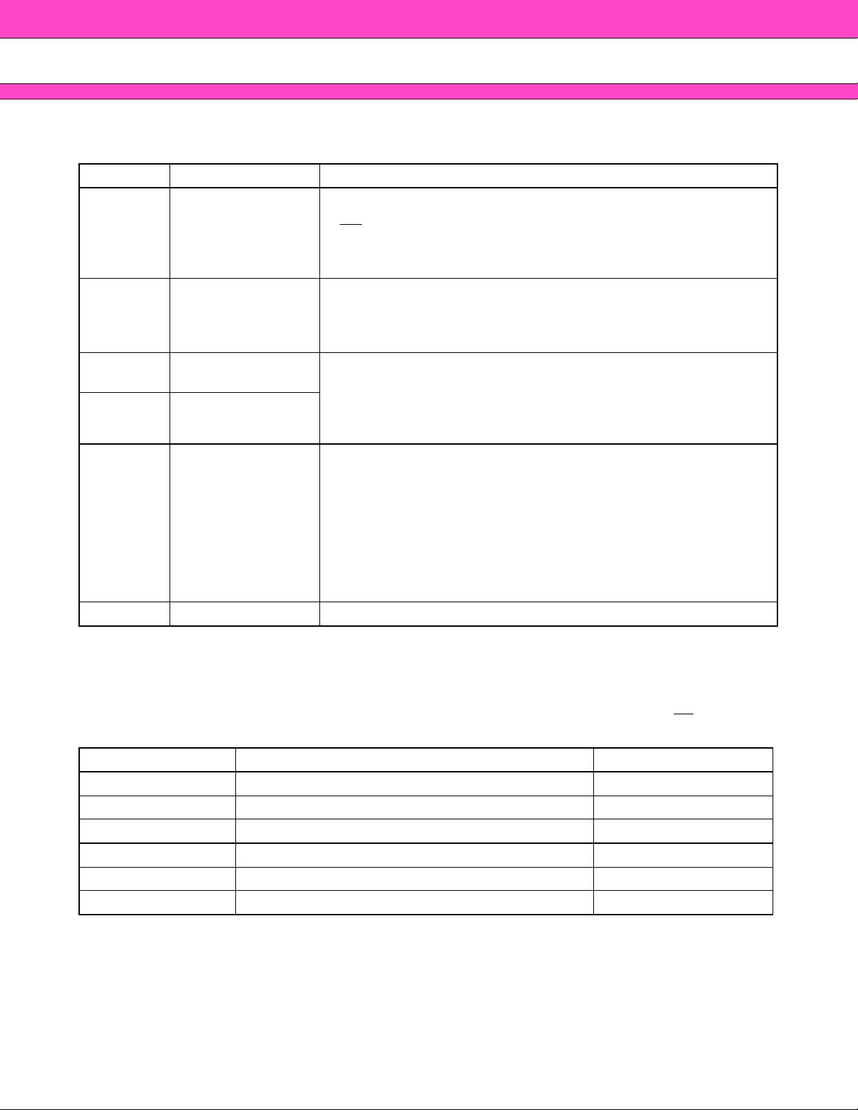
• READ
The READ command reads FRAM memory cell array data. Arbitrary 16 bits address and op-code of READ are
input to SI. The most significant address bit is invalid. Then, 8-cycle clock is input to SCK. SO is output synchronously to the falling edge of SCK. While reading, the SI value is invalid. When CS
is completed, but keep on reading address with automatic increment is enabled by continuously sending clock
for 8 cycles each to SCK before CS
is risen. When it reaches the most significant address, it rolls over to come
back to the starting address, and reading cycle keeps on infinitely.
is risen, the READ command
CS
SCK
SI
SO
00 00X11210
OP-CODE
00 1 111314 35
76543210
MSB
1312111098 2524232221201918313029282726
16-bit Address
4201
LSB
High-Z
MSB
Invalid
Data Out
LSB
20136457
Invalid
• WRITE
The WRITE command writes data to FRAM memory cell array. WRITE op-code, arbitrary 16 bits of address and
8 bits of writing data are input to SI. The most significant address bit is invalid. When 8 bits of writing data is
input, data is written to FRAM memory cell array. Risen CS
continue sending the writing data for 8 bits each before CS
will terminate the WRITE command, but if you
is risen, it is possible to continue writing with automatic
address increment. When it reaches the most significant address, it rolls over, comes back to the starting address,
and writing cycle can be continued infinitely.
CS
SCK
SI
SO
76543210
00 00X11210
OP-CODE
00 0 111314 35
MSB
1312111098 2524232221201918313029282726
16-bit Address
4201
MSB
High-Z
LSB
Data In
20136457
LSB
9
MB85RS256
■ BLOCK PROTECT
Writing protect block is configured by the WRITE command with BP1, BP0 value of the status register.
BP1 BP0 Protected Block
00None
0 1 6000
1 0 4000H to 7FFFH (upper 1/2)
1 1 0000
H to 7FFFH (upper 1/4)
H to 7FFFH (all)
■ WRITING PROTECT
Writing operation of the WRITE command and the WRSR command are protected with the value of WEL, WPEN,
WP
as shown in the table.
WEL WPEN WP
0 X X Protected Protected Protected
1 0 X Protected Unprotected Unprotected
1 1 0 Protected Unprotected Protected
1 1 1 Protected Unprotected Unprotected
Protected Blocks Unprotected Blocks Status Register
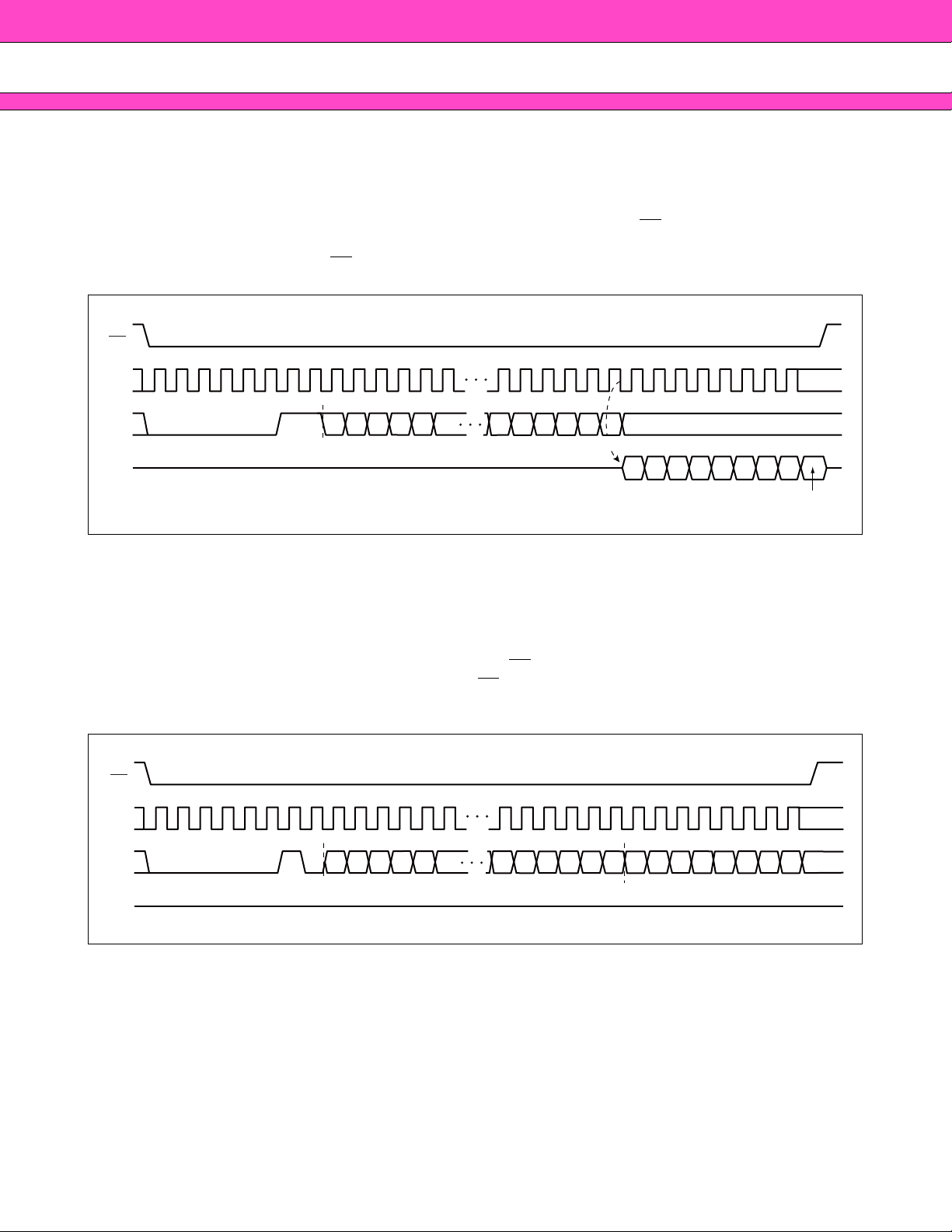
■ HOLD OPERATION
Hold status is retained without aborting a command if HOLD is “L” while CS is “L”. The timing for starting and
ending hold status depends on the SCK to be “H” or “L” when a HOLD
diagram below. Arbitrary command operation is interrupted in hold status, SCK and SI inputs become don’t care.
And, SO becomes High-Z while reading command (RDSR, READ) . If CS
is aborted and device is reset.
pin input is transited as shown in the
is risen with hold status, a command
10
CS
SCK
HOLD
Hold Condition
Hold Condition

■ ABSOLUTE MAXIMUM RATINGS
MB85RS256
Parameter Symbol
Unit
Min Max
Rating
Power supply voltage V
Input voltage V
Output voltage V
DD − 0.5 + 4.0 V
IN − 0.5 VDD + 0.5 V
OUT − 0.5 VDD + 0.5 V
Operating temperature TA − 20 + 85 °C
Storage temperature Tstg − 20 + 85 °C
WARNING: Semiconductor devices can be permanently damaged by application of stress (voltage, current,
temperature, etc.) in excess of absolute maximum ratings. Do not exceed these ratings.
■ RECOMMENDED OPERATING CONDITIONS
Parameter Symbol
Power supply voltage V
Input high voltage V
Input low voltage V
Min Typ Max
DD 3.0 3.3 3.6 V
IH 0.8 × VDD ⎯ VDD + 0.5 V
IL − 0.5 ⎯ + 0.6 V
Val ue
Unit
Operating temperature T
A − 20 ⎯ + 85 °C
WARNING: The recommended operating conditions are required in order to ensure the normal operation of the
semiconductor device. All of the device’s electrical characteristics are warranted when the device is
operated within these ranges.
Always use semiconductor devices within their recommended operating condition ranges. Operation
outside these ranges may adversely affect reliability and could result in device failure.
No warranty is made with respect to uses, operating conditions, or combinations not represented on
the data sheet. Users considering application outside the listed conditions are advised to contact their
FUJITSU representatives beforehand.
11
MB85RS256
■ ELECTRICAL CHARACTERISTICS
1. DC Characteristics
Parameter Symbol Condition
(within recommended operating conditions)
Value
Unit
Min Typ Max
Input leakage current I
LI VIN = 0 V to VDD ⎯⎯10 µA
Output leakage current ILO VOUT = 0 V to VDD ⎯⎯10 µA
Operating power supply current I
Standby current I
DD SCK = 15 MHz ⎯ 510mA
SB
All inputs VSS or
SCK = SI = CS
= VDD
⎯ 350µA
Output high voltage VOH IOH = −0.1 mA VDD × 0.8 ⎯⎯V
Output low voltage V
OL IOL = 2 mA ⎯⎯0.4 V
12

2. AC Characteristics
Parameter Symbol
MB85RS256
(within recommended operating conditions)
Value
Unit
Min Max
SCK clock frequency f
Clock high time t
Clock low time t
CK 015MHz
CH 30 ⎯ ns
CL 30 ⎯ ns
Chip select set up time tCSU 10 ⎯ ns
Chip select hold time t
Output disable time t
CSH 10 ⎯ ns
OD ⎯ 20 ns
Output data valid time tODV ⎯ 35 ns
Output hold time t
Deselect time t
OH 0 ⎯ ns
D 60 ⎯ ns
Data in rise time tR ⎯ 50 ns
Data fall time t
Data set up time t
F ⎯ 50 ns
SU 5 ⎯ ns
Data hold time tH 5 ⎯ ns
HOLD
set up time tHS 10 ⎯ ns
HOLD
hold time tHH 10 ⎯ ns
HOLD
output floating time tHZ ⎯ 20 ns
HOLD output active time tLZ ⎯ 20 ns
AC Test Condition
Power supply voltage : 3.0 V to 3.6 V
Operation temperature : − 20 °C to + 85 °C
Input voltage magnitude : 0.3 V to 2.7 V
Input rise time : 5 ns
Input fall time : 5 ns
Input judge level : V
Output judge level : V
DD/2
DD/2
13

MB85RS256
AC Load Equivalent Circuit
3.3 V
1.2 k
Output
30 pF
0.95 k
3. Pin Capacitance
Parameter Symbol
Output capacitance C
Input capacitance CI ⎯ 10 pF
O ⎯ 10 pF
Min Max
Value
Unit
14

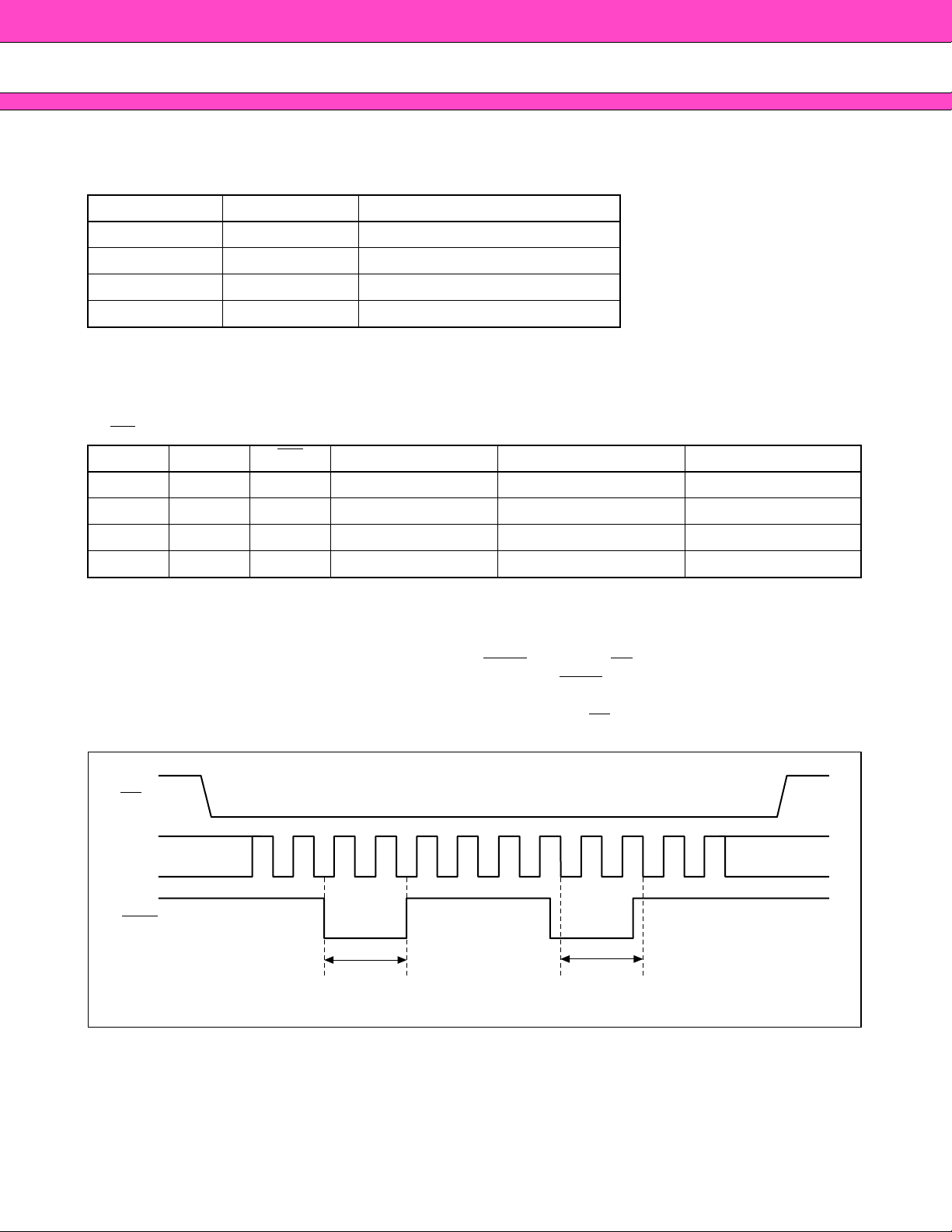
■ TIMING DIAGRAM
• Serial Data Timing
CS
SCK
t
CSU
t
SUtH
MB85RS256
t
D
t
CSH
t
CH
t
CL
SI
SO
• Hold Timing
CS
SCK
High-Z
: don't care
Valid in
t
HS tHS
t
ODV
t
OH
t
OD
High-Z
tHS tHS
tHHtHH
tHH tHH
HOLD
SO
High-ZHigh-Z
tHZ tLZ tHZ tLZ
15

MB85RS256
■ POWER ON/OFF SEQUENCE
tpd
DD
V
3.0 V
V
IH
(Min)
1.0 V
IL
(Max)
V
GND
CS CS
CS >V
* : CS (Max) < VDD + 0.5 V
DD
× 0.8 *
CS : don't care
CS >V
DD
× 0.8 *
tpu
Parameter Symbol
CS
level hold time at power OFF tpd 85 ⎯ ns
CS
level hold time at power ON tpu 85 ⎯ ns
■ NOTES ON USE
After IR reflow, the hold of data that was written before IR reflow is not guaranteed.
16
Value
Unit
Min Max

■ ORDERING INFORMATION
Part number Package
MB85RS256PNF-G-JNE1
MB85RS256
8-pin plastic SOP
(FPT-8P-M02)
17

MB85RS256
■ PACKAGE DIMENSION
8-pin plastic SOP Lead pitch 1.27 mm
8-pin plastic SOP
(FPT-8P-M02)
+0.25
1
*
–0.20
5.05
(FPT-8P-M02)
+.010
–.008
.199
58
Package width
package length
×
3.9 × 5.05 mm
Lead shape Gullwing
Sealing method Plastic mold
Mounting height 1.75 mm MAX
Weight 0.06 g
Note 1)*1 : These dimensions include resin protrusion.
Note 2)*2 : These dimensions do not include resin protrusion.
Note 3)Pins width and pins thickness include plating thickness.
Note 4) Pins width do not include tie bar cutting remainder.
0.22
.009
+0.03
–0.07
+.001
–.003
2
*
3.90±0.30 6.00±0.40
(.154±.012) (.236±.016)
0.40(.016)
14
1.27(.050)
C
2002 FUJITSU LIMITED F08004S-c-4-7
0.10(.004)
0.10(.004)
0.44±0.08
(.017±.003)
0.13(.005)
M
Please confirm the latest Package dimension by following URL.
http://edevice.fujitsu.com/fj/DATASHEET/ef-ovpklv.html
18
45˚
Details of "A" part
1.55±0.20
(.061±.008)
"A"
Dimensions in mm (inches).
Note: The values in parentheses are reference values.
0~8
0.50±0.20
(.020±.008)
0.60±0.15
(.024±.006)
0.25(.010)
˚
(Mounting height)
0.15±0.10
(.006±.004)
(Stand off)

MB85RS256
FUJITSU LIMITED
All Rights Reserved.
The contents of this document are subject to change without notice.
Customers are advised to consult with FUJITSU sales
representatives before ordering.
The information, such as descriptions of function and application
circuit examples, in this document are presented solely for the
purpose of reference to show examples of operations and uses of
Fujitsu semiconductor device; Fujitsu does not warrant proper
operation of the device with respect to use based on such
information. When you develop equipment incorporating the
device based on such information, you must assume any
responsibility arising out of such use of the information. Fujitsu
assumes no liability for any damages whatsoever arising out of
the use of the information.
Any information in this document, including descriptions of
function and schematic diagrams, shall not be construed as license
of the use or exercise of any intellectual property right, such as
patent right or copyright, or any other right of Fujitsu or any third
party or does Fujitsu warrant non-infringement of any third-party’s
intellectual property right or other right by using such information.
Fujitsu assumes no liability for any infringement of the intellectual
property rights or other rights of third parties which would result
from the use of information contained herein.
The products described in this document are designed, developed
and manufactured as contemplated for general use, including
without limitation, ordinary industrial use, general office use,
personal use, and household use, but are not designed, developed
and manufactured as contemplated (1) for use accompanying fatal
risks or dangers that, unless extremely high safety is secured, could
have a serious effect to the public, and could lead directly to death,
personal injury, severe physical damage or other loss (i.e., nuclear
reaction control in nuclear facility, aircraft flight control, air traffic
control, mass transport control, medical life support system, missile
launch control in weapon system), or (2) for use requiring
extremely high reliability (i.e., submersible repeater and artificial
satellite).
Please note that Fujitsu will not be liable against you and/or any
third party for any claims or damages arising in connection with
above-mentioned uses of the products.
Any semiconductor devices have an inherent chance of failure. You
must protect against injury, damage or loss from such failures by
incorporating safety design measures into your facility and
equipment such as redundancy, fire protection, and prevention of
over-current levels and other abnormal operating conditions.
If any products described in this document represent goods or
technologies subject to certain restrictions on export under the
Foreign Exchange and Foreign Trade Law of Japan, the prior
authorization by Japanese government will be required for export
of those products from Japan.
The company names and brand names herein are the trademarks or
registered trademarks of their respective owners.
Edited Business Promotion Dept.
F0702
 Loading...