


FUJITSU SEMICONDUCTOR
DATA SHEET
Memory FRAM
CMOS
1 M Bit (64 K × 16)
MB85R1002
■ DESCRIPTIONS
The MB85R1002 is an FRAM (Ferroelectric Random Access Memory) chip consisting of 65,536 words x 16 bits
of non-volatile memory cells created using ferroelectric process and silicon gate CMOS process technologies.
The MB85R1002 is able to retain data without using a back-up battery, as is needed for SRAM.
The memory cells used in the MB85R1002 can be used for at least 10
improvement over the number of read and write operations supported by Flash memory and E
The MB85R1002 uses a pseudo-SRAM interface that is compatible with conventional asynchronous SRAM.
DS05-13104-3E
10
read/write operations, which is a significant
2
PROM.
■ FEATURES
• Bit configuration : 65,536 words × 16 bits
• Read/write endurance : 10
• Operating power supply voltage : 3.0 V to 3.6 V
• Operating temperature range : − 20 °C to +85 °C
• Data retention : 10 years (+55 °C)
•LB
and UB data byte control
• Package : 48-pin plastic TSOP (1)
10
times/bit (Min)
: 48-pin plastic FBGA
Copyright©2005-2007 FUJITSU LIMITED All rights reserved
MB85R1002
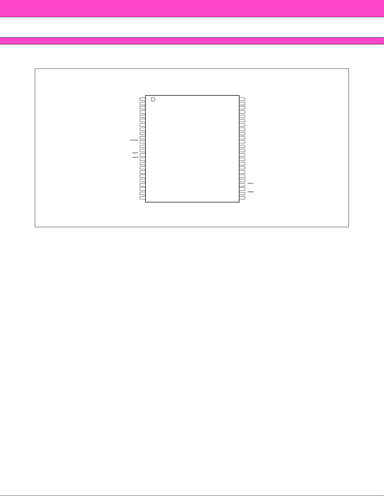
■ PIN ASSIGNMENT
A15
A14
A13
A12
A11
A10
A9
A8
NC
NC
WE
CE2
GND
UB
LB
V
NC
A7
A6
A5
A4
A3
A2
A1
(
TOP VIEW)
1
2
3
4
5
6
7
8
9
10
11
12
13
14
15
16
CC
17
18
19
20
21
22
23
24
48
NC
47
NC
46
GND
45
I/O16
44
I/O8
43
I/O15
42
I/O7
41
I/O14
40
I/O6
39
I/O13
38
I/O5
37
V
CC
36
I/O12
35
I/O4
34
I/O11
33
I/O3
32
I/O10
31
I/O2
30
I/O9
29
I/O1
28
OE
27
GND
26
CE1
25
A0
(FPT-48P-M25)
(Continued)
2
(Continued)
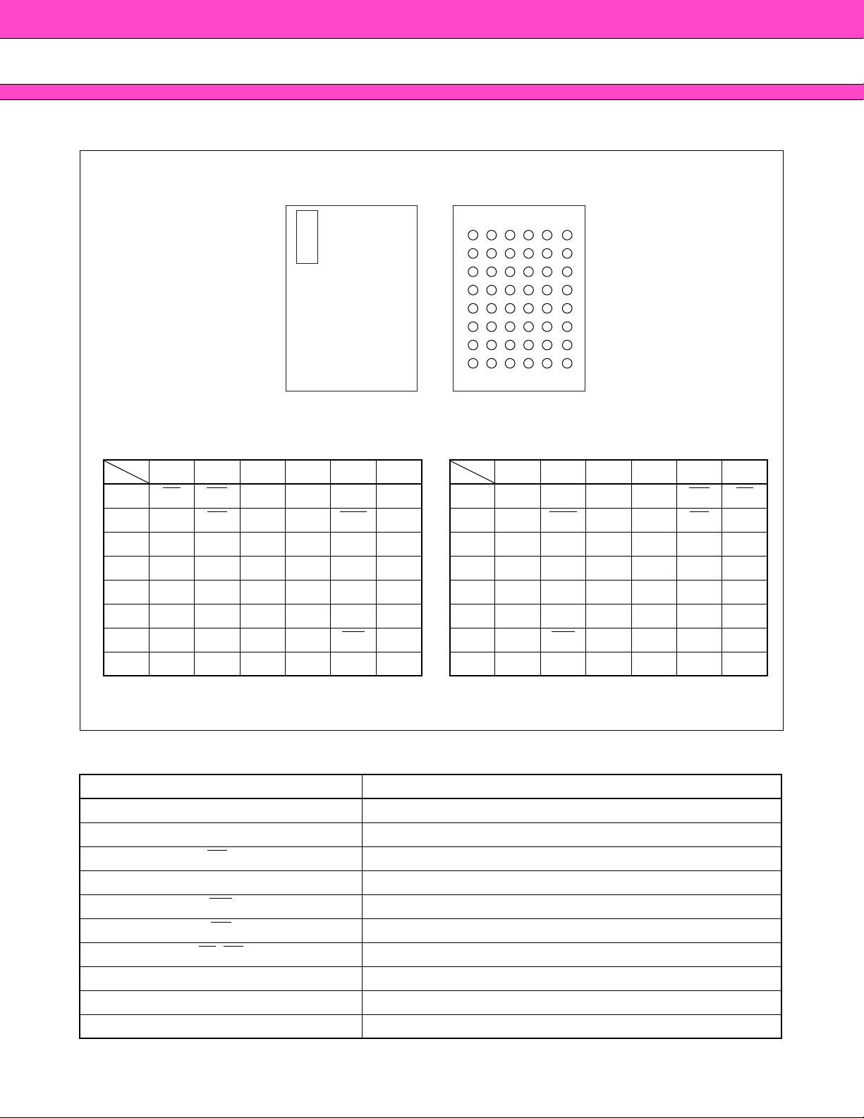
MB85R1002
Top View Bottom View
INDEX
A
B
C
D
E
F
G
H
6543 21123 456
12 3456 654321
ALB
OE A0 A1 A2 CE2 A CE2 A2 A1 A0 OE LB
BI/O9UBA3 A4 CE1 I/O1 B I/O1 CE1 A4 A3 UB I/O9
C I/O10 I/O11 A5 A6 I/O2 I/O3 C I/O3 I/O2 A6 A5 I/O11 I/O10
D GND I/O12 NC A7 I/O4 V
EV
CC I/O13 NC NC I/O5 GND E GND I/O5 NC NC I/O13 VCC
CC DVCC I/O4 A7 NC I/O12 GND
F I/O15 I/O14 A14 A15 I/O6 I/O7 F I/O7 I/O6 A15 A14 I/O14 I/O15
G I/O16 NC A12 A13 WE I/O8 G I/O8 WE A13 A12 NC I/O16
H NC A8 A9 A10 A11 NC H NC A11 A10 A9 A8 NC
(BGA-48P-M23)
■ PIN DESCRIPTION
Pin name Function
A0 to A15 Address In
I/O1 to I/O16 Data Input/Output
CE
1 Chip Enable 1 in
CE2 Chip Enable 2 in
WE
OE
Write Enable in
Output Enable in
LB, UB Data Byte Control in
V
CC Power Supply
GND Ground
NC No Connection
3
MB85R1002
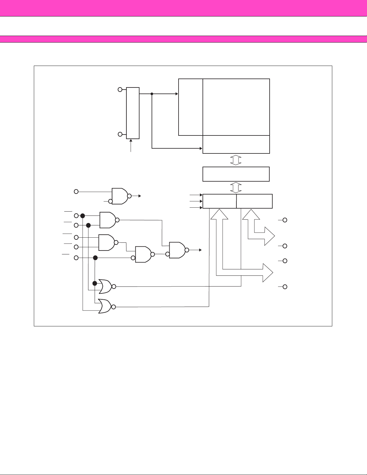
■ BLOCK DIAGRAM
A0
CE2
LB
UB
WE
OE
CE1
intCEB
to
A15
·
·
·
intCE2
Address Latch.
intCE2
Row Dec.
intOE
intWE
intCE2
intCEB
Ferro Capacitor Cell
Column Dec.
S/A
I/O1 to I/O8
I/O9 to I/O16
·
·
·
·
I/O16
to
I/O9
I/O8
to
I/O1
4
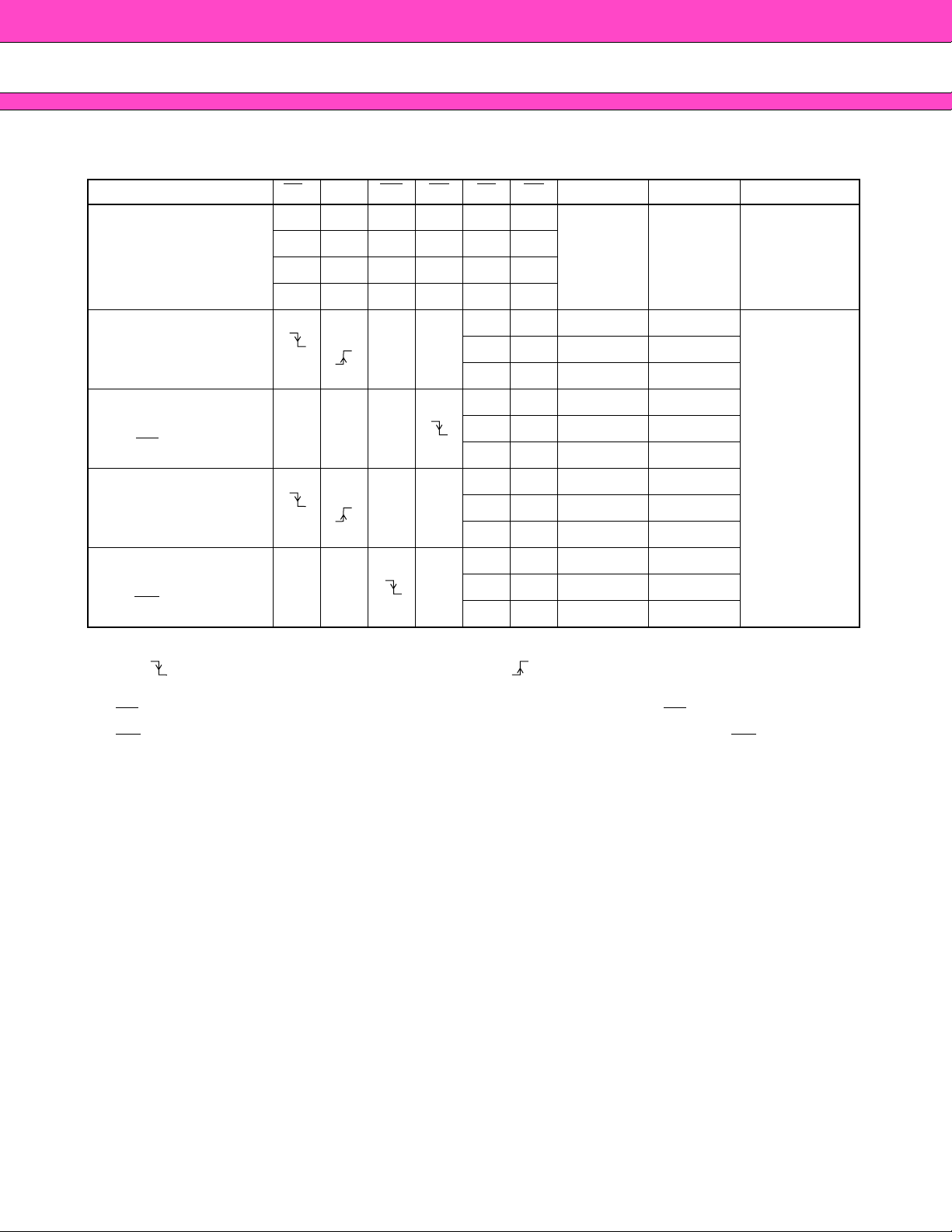
■ FUNCTION TRUTH TABLE
Mode CE1CE2 WE OE LB UB I/O1 to I/O8 I/O9 to I/O16 Supply Current
HXXXXX
MB85R1002
Standby Pre-charge
Read
Read
(Pseudo-SRAM,
OE
control*1)
Write
Write
(Pseudo-SRAM,
WE
control*2)
Notes : L = VIL, H = VIH, X can be either VIL or VIH, High-Z = High Impedance
: Latch address and latch data at falling edge, : Latch address and latch data at rising edge
XLXXXX
XXHHXX
XXXXHH
L L Dout Dout
H
L
LHH
H
L
LH H
HL
LX
L H Dout High-Z
H L High-Z Dout
L L Dout Dout
L H Dout High-Z
H L High-Z Dout
LL Din Din
L H Din High-Z
HL High-Z Din
LL Din Din
L H Din High-Z
HL High-Z Din
High-Z High-Z
Standby
(ISB)
Operation
(I
CC)
*1 : OE
*2 : WE
control of the Pseudo-SRAM means the valid address at the falling edge of OE to read.
control of the Pseudo-SRAM means the valid address and data at the falling edge of WE to write.
5

MB85R1002
■ ABSOLUTE MAXIMUM RATINGS
Parameter Symbol
Unit
Min Max
Rating
Supply Voltage* V
Input Voltage* V
Output Voltage* V
Ambient Operating Temperature TA −20 +85
Storage Temperature T
CC −0.5 +4.0 V
IN −0.5 VCC + 0.5 V
OUT −0.5 VCC + 0.5 V
o
stg −40 +125
o
C
C
* : All voltages are referenced to GND.
WARNING: Semiconductor devices can be permanently damaged by application of stress (voltage, current,
temperature, etc.) in excess of absolute maximum ratings. Do not exceed these ratings.
■ RECOMMENDED OPERATING CONDITIONS
Parameter Symbol
Supply Voltage* V
Input Voltage (high)* V
Input Voltage (low)* V
Ambient Operating Temperature T
Min Typ Max
CC 3.0 3.3 3.6 V
IH VCC × 0.8 ⎯ VCC + 0.5 V
IL −0.5 ⎯+0.6 V
A − 20 ⎯+85
Val ue
Unit
o
C
* : All voltages are referenced to GND.
WARNING: The recommended operating conditions are required in order to ensure the normal operation of the
semiconductor device. All of the device’s electrical characteristics are warranted when the device is
operated within these ranges.Always use semiconductor devices within their recommended operating
condition ranges. Operation outside these ranges may adversely affect reliability and could result in
device failure.
No warranty is made with respect to uses, operating conditions, or combinations not represented on
the data sheet. Users considering application outside the listed conditions are advised to contact their
FUJITSU representatives beforehand.
6

■ ELECTRICAL CHARACTERISTICS
MB85R1002
1. DC CHARACTERISTICS
(within recommended operating conditions)
Parameter Symbol Test Conditions
Input Leakage Current |I
LI|VIN = 0 V to VCC ⎯⎯10 µA
Output Leakage Current |ILO|VOUT = 0 V to VCC, CE1 = VIH or OE = VIH ⎯⎯10 µA
Operating Power Supply
Current
I
CC CE1 = 0.2 V, CE2 = VCC−0.2 V, Iout = 0 mA*
1
CE1 ≥ VCC−0.2 V
2
2
2
Standby Current I
CE2 ≤ 0.2 V*
SB
OE ≥ VCC−0.2 V, WE ≥ VCC−0.2 V*
LB ≥ VCC−0.2 V, UB ≥ VCC−0.2 V*
Output Voltage (high) VOH IOH = −0.1 mA VCC × 0.8 ⎯⎯ V
Output Voltage (low) V
*1 : During the measurement of I
OL IOL = 2.0 mA ⎯⎯0.4 V
CC , the Address, Data In were taken to only change once per active cycle.
Iout : output current
*2 : All pins other than setting pins should be input at the CMOS level voltages such as H ≥ V
Val ue
Unit
Min Typ Max
⎯ 10 15 mA
⎯ 10 50 µA
CC − 0.2 V, L ≤ 0.2 V.
7

MB85R1002
2. AC TEST CONDITIONS
Supply Voltage : 3.0 V to 3.6 V
Operating Temperature : −20
Input Voltage Amplitude : 0.3 V to 2.7 V
Input Rising Time : 5 ns
Input Falling Time : 5 ns
Input Evaluation Level : 2.0 V / 0.8 V
Output Evaluation Level : 2.0 V / 0.8 V
Output Impedance : 50 pF
o
C to +85 oC
(1) Read Operation
(within recommended operating conditions)
Val ue
Parameter Symbol
Min Max
Read Cycle time t
CE
1 Active Time tCA1 120 ⎯ ns
CE2 Active Time t
OE
Active Time tRP 120 ⎯ ns
LB
, UB Active Time tBP 120 ⎯ ns
Pre-charge Time t
Address Setup Time t
Address Hold Time t
OE
Setup Time tES 0 ⎯ ns
LB
, UB Setup Time tBS 5 ⎯ ns
Output Data Hold time t
Output Set Time t
CE
1 Access Time tCE1 ⎯ 100 ns
CE2 Access Time t
OE
Access Time tOE ⎯ 100 ns
Output Floating Time t
RC 150 ⎯ ns
CA2 120 ⎯ ns
PC 20 ⎯ ns
AS 0 ⎯ ns
AH 50 ⎯ ns
OH 0 ⎯ ns
LZ 30 ⎯ ns
CE2 ⎯ 100 ns
OHZ ⎯ 20 ns
Unit
8

(2) Write Operation
MB85R1002
(within recommended operating conditions)
Parameter Symbol
Value
Min Max
Write Cycle Time t
CE
1 Active Time tCA1 120 ⎯ ns
CE2 Active Time t
LB
, UB Active Time tBP 120 ⎯ ns
Pre-Charge Time t
Address Setup Time t
Address Hold Time t
LB
, UB Setup Time tBS 5 ⎯ ns
Write Pulse Width t
Data Setup Time t
Data Hold Time t
Write Setup Time t
WC 150 ⎯ ns
CA2 120 ⎯ ns
PC 20 ⎯ ns
AS 0 ⎯ ns
AH 50 ⎯ ns
WP 120 ⎯ ns
DS 0 ⎯ ns
DH 50 ⎯ ns
WS 0 ⎯ ns
(3) Power ON/OFF Sequence
(within recommended operating conditions)
Parameter
1 LEVEL hold time for Power OFF tpd 85 ⎯⎯ns
CE
Sym-
bol
Min Typ Max
Val ue
Unit
Unit
CE
1 LEVEL hold time for Power ON tpu 85 ⎯⎯ns
3. Pin Capacitance
(f = 1 MHz, TA = +25 oC)
Parameter Symbol Test Condition
Input Capacitance C
Output Capacitance C
Min Typ Max
IN VIN = GND ⎯⎯10 pF
OUT VOUT = GND ⎯⎯10 pF
Val ue
Unit
9

MB85R1002
■ TIMING DIAGRAMS
1. Read Cycle Timing 1 (CE
CE1
CE2
tBS
LB, UB
tAS tAH
A0 to A15
OE
I/O1 to I/O16
Valid
tES
1, CE2 Control)
tCE1,
tCE2
tLZ
tRC
tCA1
tCA2
tBP
H or L
tRP
tOH
Valid
Invalid Invalid
tPC
tOHZ
High-Z
2. Read Cycle Timing 2 (OE
CE1
CE2
t
LB, UB
t
A0 to A15
OE
I/O1 to I/O16
Valid H or L
Control)
BS
AS
t
AH
t
CA1
t
CA2
t
BP
t
RC
t
t
OHZ
PC
High-Z
t
RP
t
OE
t
t
LZ
Invalid Invalid
OH
Valid
10

3. Write Cycle Timing 1 (CE1, CE2 Control)
CE1
t
CA1
MB85R1002
t
WC
t
PC
CE2
LB, UB
A0 to A15
WE
Data In
4. Write Cycle Timing 2 (WE
CE1
t
BS
t
t
AS
AH
Valid H or L
t
WS
t
DS
t
DH
Valid H or L
Control)
t
t
CA1
CA2
t
BP
t
WP
High-Z
CE2
LB, UB
A0 to A15
WE
Data In
t
CA2
t
t
BS
t
t
AS
AH
BP
Valid H or L
t
WP
t
DS
t
DH
Valid H or L
t
WC
t
PC
High-Z
11

MB85R1002
■ POWER ON/OFF SEQUENCE
V
CC
CE2
3.0 V
tputpd
V
CC
CE2
3.0 V
VIH (Min)
1.0 V
V
IL
(Max)
GND
CE1
CE2 ≤ 0.2 V
CE1 > VCC × 0.8* CE1 : Don't Care CE1 > VCC × 0.8*
* : CE1 (Max) < VCC + 0.5 V
Note : You can choose either of CE
1 or CE2, or both for disenable control of the device.
■ NOTES ON USE
Data that is written prior to IR reflow is not guaranteed to be retained after IR reflow.
CE1
VIH (Min)
1.0 V
V
IL
(Max)
GND
■ ORDERING INFOMATION
Part number Package
MB85R1002PFTN-GE1
MB85R1002BGT-GE1
12
48-pin plastic TSOP(1)
(FPT-48P-M25)
48-pin plastic FBGA
(BGA-48P-M23)
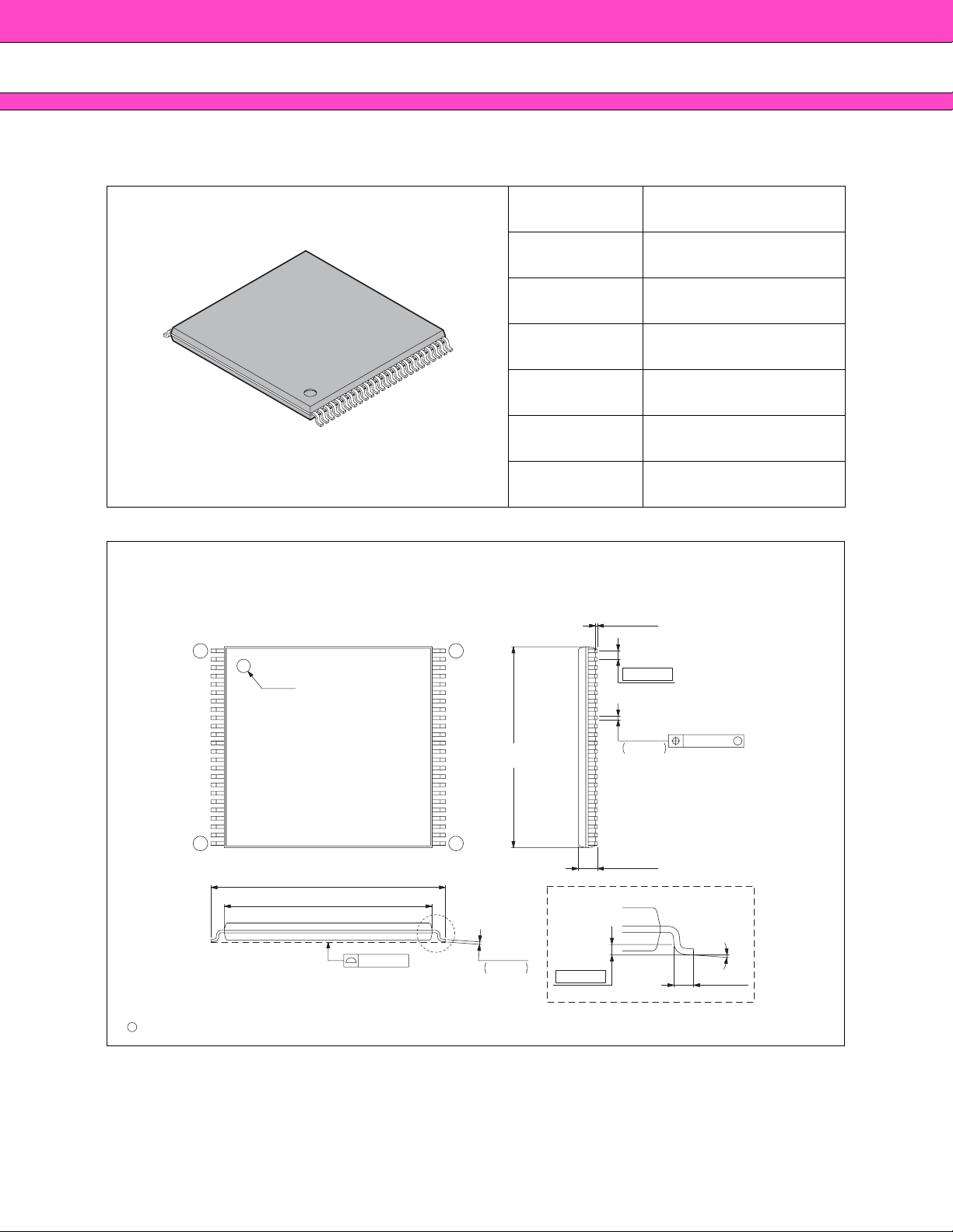
■ PACKAGE DIMENSIONS
48-pin plastic TSOP(1) Lead pitch 0.50 mm
MB85R1002
(FPT-48P-M25)
48-pin plastic TSOP(1)
(FPT-48P-M25)
LEAD No.
1 48
INDEX
Package width ×
package length
12.00 × 12.40 mm
Lead shape Gullwing
Sealing method Plastic mold
Mounting height 1.20 mm MAX
Weight 0.37 g
Code
(Reference)
Note 1)*1 : Resin protrusion. (Each side : +0.15 (.006) Max).
Note 2)*2 : These dimensions do not include resin protrusions.
Note 3) Pin widths and pin thicknesses include plating thickness.
Note 4) Pin widths do not include tie bar cutting burrs.
P-TSOP(1)48-12×12.4-0.50
0.10±0.05
(.004±.002)
(Stand off)
0.50(.020)
1
*
12.00±0.10
(.472±.004)
24
*
C
2003 FUJITSU LIMITED F48043S-c-2-2
14.00±0.20(.551±.008)
2
12.40±0.10(.488±.004)
0.08(.003)
25
"A"
+0.05
–0.03
0.145
+.002
.006
–.001
Please confirm the latest Package dimension by following URL.
http://edevice.fujitsu.com/fj/DATASHEET/ef-ovpklv.html
+0.05
0.22
–0.04
0.10(.004)
+.002
–.002
.009
1.13±0.07
(.044±.003)
Details of "A" part
0.25(.010)
Dimensions in mm (inches).
Note: The values in parentheses are reference values
(Mounting height)
M
0
˚~8˚
0.60±0.15
(.024±.006)
(Continued)
13

MB85R1002
(Continued)
48-pin plastic FBGA Lead pitch 0.75 mm
(BGA-48P-M23)
48-pin plastic FBGA
(BGA-48P-M23)
8.10±0.20(.319±.008)
6.10±0.20
.008)
(.240
±
Package width ×
package length
8.10 mm × 6.10 mm
Lead shape Ball
Sealing method Plastic mold
Mounting height 1.10 mm Max
Weight 0.08 g
+.006
+0.15
.043 –.004
–0.10
0.95
(Mounting height)
0.25±0.10(.010±.004)
(Stand off)
A
3.75
(.148)
5.25(.207)
0.75(.030)TYP
B
6
5
4
3
2
1
(INDEX AREA)
0.10(.004)
C
2007 FUJITSU LIMITED B48023S-c-1-1
S
Please confirm the latest Package dimension by following URL.
http://edevice.fujitsu.com/fj/DATASHEET/ef-ovpklv.html
14
HGFEDCBA
0.35±0.05
48-
ø
(48-ø.014±.002)
Dimensions in mm (inches).
Note: The values in parentheses are reference values.
0.08(.003) S A
ø
M
B

MB85R1002
FUJITSU LIMITED
All Rights Reserved.
The contents of this document are subject to change without notice.
Customers are advised to consult with FUJITSU sales
representatives before ordering.
The information, such as descriptions of function and application
circuit examples, in this document are presented solely for the
purpose of reference to show examples of operations and uses of
Fujitsu semiconductor device; Fujitsu does not warrant proper
operation of the device with respect to use based on such
information. When you develop equipment incorporating the
device based on such information, you must assume any
responsibility arising out of such use of the information. Fujitsu
assumes no liability for any damages whatsoever arising out of
the use of the information.
Any information in this document, including descriptions of
function and schematic diagrams, shall not be construed as license
of the use or exercise of any intellectual property right, such as
patent right or copyright, or any other right of Fujitsu or any third
party or does Fujitsu warrant non-infringement of any third-party’s
intellectual property right or other right by using such information.
Fujitsu assumes no liability for any infringement of the intellectual
property rights or other rights of third parties which would result
from the use of information contained herein.
The products described in this document are designed, developed
and manufactured as contemplated for general use, including
without limitation, ordinary industrial use, general office use,
personal use, and household use, but are not designed, developed
and manufactured as contemplated (1) for use accompanying fatal
risks or dangers that, unless extremely high safety is secured, could
have a serious effect to the public, and could lead directly to death,
personal injury, severe physical damage or other loss (i.e., nuclear
reaction control in nuclear facility, aircraft flight control, air traffic
control, mass transport control, medical life support system, missile
launch control in weapon system), or (2) for use requiring
extremely high reliability (i.e., submersible repeater and artificial
satellite).
Please note that Fujitsu will not be liable against you and/or any
third party for any claims or damages arising in connection with
above-mentioned uses of the products.
Any semiconductor devices have an inherent chance of failure. You
must protect against injury, damage or loss from such failures by
incorporating safety design measures into your facility and
equipment such as redundancy, fire protection, and prevention of
over-current levels and other abnormal operating conditions.
If any products described in this document represent goods or
technologies subject to certain restrictions on export under the
Foreign Exchange and Foreign Trade Law of Japan, the prior
authorization by Japanese government will be required for export
of those products from Japan.
The company names and brand names herein are the trademarks or
registered trademarks of their respective owners.
Edited Business Promotion Dept.
F0708
 Loading...