

Page 1

Fujitsu ASSP Product
Power Management
Evaluation Board Manual
Evaluation Board Manual
MB39C026
MB39C026
1/14
(SON--
(SON
MB39C022--
MB39C022
(MB39C026 and MB39C022 share the same evaluation board)
(MB39C026 and MB39C022 share the same evaluation board)
Rev 1.0E
June, 2008
10)
10)
EVB03
EVB03
MB39C026 Evaluation Board
Page 2
Fujitsu ASSP Product
Power Management
1. Description
1. Description
The MB39C026 is a two channels power supply IC. It consists of one channel
DC/DC Converter and one channel LDO regulator. The DC/DC converter has fast
line transient response and load regulation with current mode control topology.
Moreover, the integrated LDO provides an auxiliary output supply for noise
sensitive circuit.
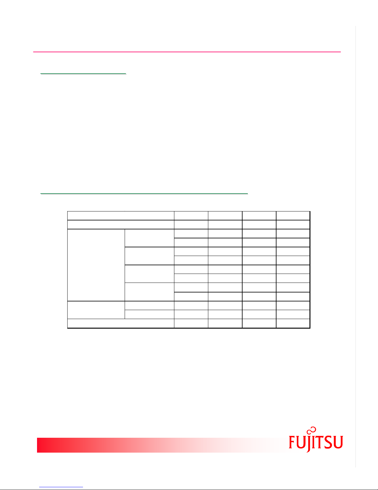
2. Evaluation Board Specification
2. Evaluation Board Specification
Parameter
Input Voltage
Output Voltage
Output Current
Oscillation Frequency
MB39C026G
MB39C026J
MB39C026L
MB39C026N
CH1 0 - 600
CH2 0 - 300
CH1 0.8 1.2 5*
CH2 3.3#
CH1 0.8 1.2 5*
CH2 2.85
CH1 0.8 1.2 5*
CH2 1.8
CH1 0.8 1.8 5*
CH2 1.2
Min. Typ. Max.
3.2 3.7 5.5
- 2.0 -
2/14
* CH1 Remark:
Maximum Output voltage is limited by the input voltage (VIN). The maximum
voltage CH1 could reach is 0.5V less than VIN.
# CH2 Remark:
The CH2 output voltage is limited by input voltage (VIN). The CH2 dropout of
MB39C026G is Vdrop. Thus the minimum input voltage should be Vdrop above
the CH2 output. Vdrop is 0.2V(Typ).
MB39C026 Evaluation Board
Page 3
Fujitsu ASSP Product
Power Management
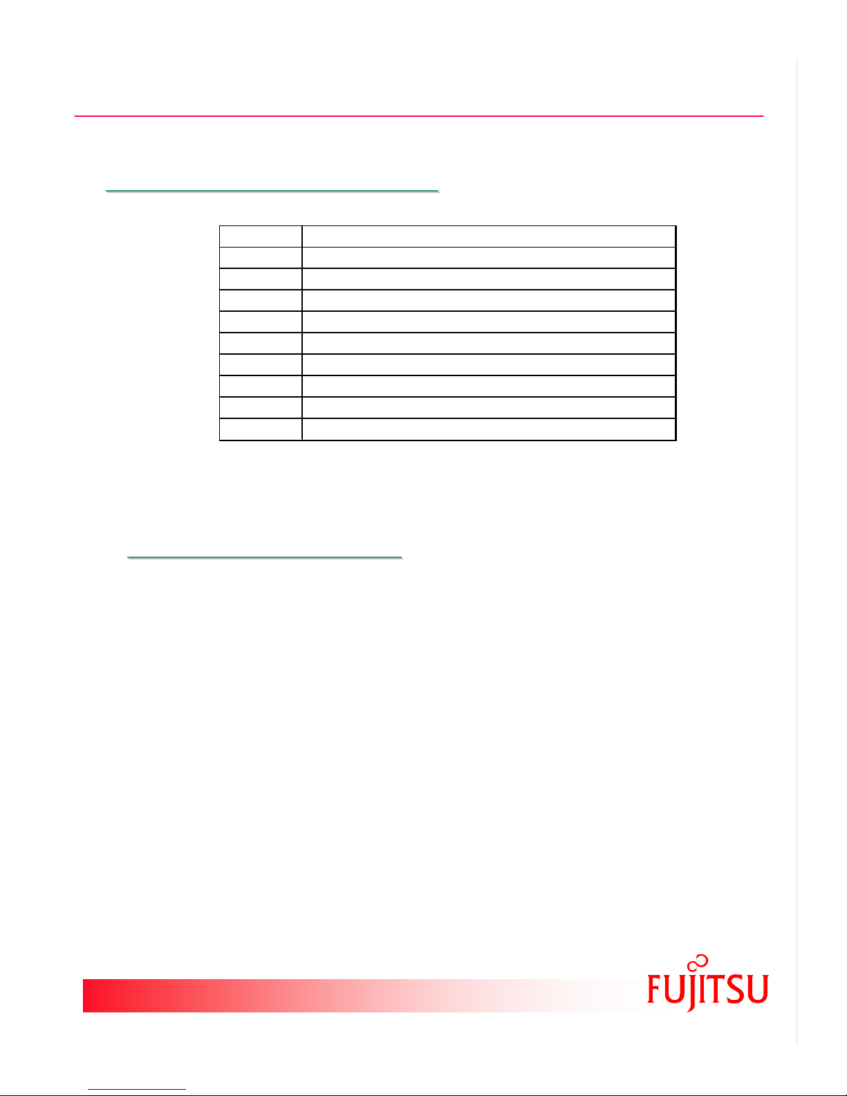
3. Terminal information
3. Terminal information
Pin Name Description
VIN Input voltage terminal
PGND Ground terminal for power supply
VO1 CH1 DC/DC converter output terminal
PGND1 Ground terminal for CH1 DC/DC converter
VO2 CH2 LDO output terminal
AGND Ground terminal for LDO output
POR Power-On-Reset output terminal
EN1 CH1 DC/DC converter control terminal
EN2 CH2 LDO control terminal
3/14
4. Setup & Checkup
4. Setup & Checkup
(1) Setup
• Connect a 3.7V power supply the VIN and PGND.
• Connect EN1 and EN2 = VIN.
• Connect VO1 and VO2 to loadings or measurement devices.
(2) Confirmation of Operation
• Turn on the power to VIN(power supply voltage).
•When IC operates normally, the voltage level at each output are as follows:
MB39C026G: VO1=1.2V, VO2=3.3V, POR=VIN
MB39C026J: VO1=1.2V, VO2=2.85V, POR=VIN
MB39C026L: VO1=1.2V, VO2=1.8V, POR=VIN
MB39C026N: VO1=1.8V, VO2=1.2V, POR=VIN
MB39C026 Evaluation Board
Page 4

Fujitsu ASSP Product
Power Management
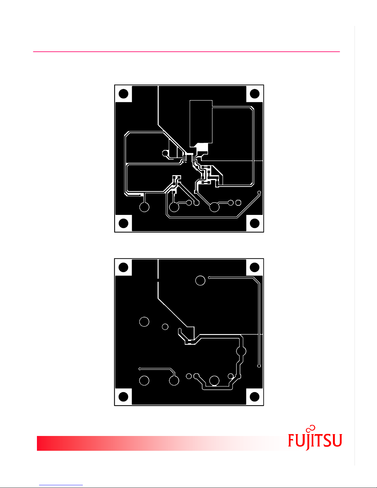
5. Evaluation Board Layout
5. Evaluation Board Layout
MB39C022-EVB03 Rev 1.0 (Top View)
4/14
Top Side Silkscreen
Bottom Side Silkscreen
MB39C026 Evaluation Board
Page 5
Fujitsu ASSP Product
Power Management
Board Layout (Top View)
MB39C022-EVB03 Rev 1.0
5/14
Top Side Metal
MB39C026 Evaluation Board
Bottom Side Metal
Page 6

Fujitsu ASSP Product
GND1
LX
FB
VOUT2
GND2
AGND
AGND
AGND
AGND
AGND
Power Management
6. Circuit Diagram
6. Circuit Diagram
VIN
C1
PGND
POR
R3
1M
JP1
JP2
: No Mount
JP3
Short
R4
1M
EN1
EN2
4.7uF
PGND
C4
1uF
R1
1M
R2
1M
VIN18
VIN22
POR4
EN17
EN21
MB39C026
(SON-10)
6/14
PGND1
10
C2
4.7uF
9
L1
2.2uH
6
VO2
3
C5
1uF
AGND
5
For VO1=1.2V: R5-1=300k
For VO1=1.8V: R5-1=499k
C6
4.7uF
R5-1
300k
or 499k
R5-2
0k
PGND
VO1
JP4
Short
R7
0R
C3
22pF
R6
100k
7. Circuit Parts List
7. Circuit Parts List
MB39C022-EVB03 Rev1.0
Count Designator Description Part Number Manufacturer
1 U1 Power IC MB39C026 Fujitsu
2 C1, C2 Capacitor 4.7uF (10V) C1608JB1A475K TDK
1 C3 Capacitor 22pF (50V) C1608CH1H220J TDK
2 C4, C5 Capacitor 1uF (16V) C1608JB1C105K TDK
1 L1 Inductor 2.2uH RDC=76m VLF4012AT-2R2M1R5 TDK
3 R1, R2, R3 Resistor 1M (1%) - -
R5-11
2 R5-2, R7 Resistor 0R - 1 R6 Resistor 100k (1%) - -
VIN, VO1, VO2,
9
POR, PGND, PGND1,
AGND, EN1, EN2
No Mount JP1, JP2 Header 1X2 - No Mount R4 1M - No Mount C6 Capacitor 4.7uF (10V) - -
Short JP3, JP4 Jumper (pattern short) - -
TDK: TDK Corporation
Resistor 300k (1%) for 1.2V output - Resistor 499k (1%) for 1.8V output
Connecting Pins WT-2-1 MacEight
MB39C026 Evaluation Board
Page 7

Fujitsu ASSP Product
()(
)
k
100
6
R
ref
Ω
Ω
Ω
()(
)
100k
R6
ref
Power Management
8. Initialization
8. Initialization
(1) Output Voltage Setting
The output voltage of VO1 can be adjusted by
the external resistor divider.
As illustrated below:
6R+5R
×
V=1VO ..
R6+R5
×
V=VO1
(2) Input Signal Setting
×V30=
×0.3V=
7/14
VO1
C2
4.7uF
FB 6
k100+k300
R5-1
300k
or
499k
R5-2
0R
R6
100k
C3
22pF
V21=
100k+499k
1.8V=
EN1
Set EN1 to VIN to start the buck DC/DC converter (VO1). R1 pull-down EN1 to
GND and disable VO1 if EN1 has no input.
EN2
Set EN2 to VIN to start the LDO converter (VO2). R2 pull-down EN2 to GND
and disable VO2 if EN2 has no input.
Power On Reset (POR)
R3 and R4 are the pull-up resistors for POR (Pin 4). A 1Mresistor is required
to placed at either R3 or R4. When R3 has a 1Mresistor and R4 is open; the
POR will be connected VIN. When R4 has a 1Mresistor and R3 is open; the
POR pin will be connected to VO1.
By default, only R3 require a 1Mresistor while R4 is open.
MB39C026 Evaluation Board
Page 8

Fujitsu ASSP Product
Power Management
9. Reference Data
9. Reference Data
(1) Efficiency
CH1 Test Condition:
EN1=VIN; EN2=0V
VO1=1.2V; C1=C2=4.7uF
CH1 Efficiency
90
80
70
60
50
40
30
Efficiency (%)
20
10
0
0.001 0.01 0.1 1
VIN=3.7V
VIN=4.3V
VIN=5.5V
IO1 Load Current (A)
CH1 Test Condition:
EN1=VIN; EN2=0V
VO1=1.8V; C1=C2=4.7uF
CH1 Efficiency
100
90
80
70
60
50
40
30
Efficienc y (%)
20
10
0
0.001 0.01 0.1 1
VIN=3.7V
VIN=4.3V
VIN=5.5V
IO1 Load Current (A)
8/14
(2) DC/DC Load Regulation
CH1 Test Condition:
EN1=VIN; EN2=0V
VO1=1.2V; C1=C2=4.7uF
CH1 Load Regulation
1.3
1.28
1.26
1.24
1.22
1.2
1.18
1.16
1.14
VO1 Output Voltage (V)
1.12
1.1
0 0.1 0.2 0.3 0.4 0.5 0.6
IO1 Load Current (A)
VIN=3.7V
VIN=4.3V
VIN=5.5V
CH1 Test Condition:
EN1=VIN; EN2=0V
VO1=1.8V; C1=C2=4.7uF
CH1 Load Regulation
1.9
1.88
1.86
1.84
1.82
1.8
1.78
1.76
1.74
VO1 Output Voltage (V)
1.72
1.7
0 0.1 0.2 0.3 0.4 0.5 0.6
IO1 Load Current (A)
VIN=3.7V
VIN=4.3V
VIN=5.5V
MB39C026 Evaluation Board
Page 9

Fujitsu ASSP Product
VO1 Output Voltage (V)
Power Management
(3) DC/DC Line Regulation
CH1 Test Condition:
EN1=VIN; EN2=0V
VO1=1.2V; C1=C2=4.7uF
CH1 Line Regulation
1.3
1.28
1.26
1.24
1.22
1.2
1.18
1.16
1.14
VO1 Output Voltage (V)
1.12
1.1
3.2 3.7 4.2 4.7 5.2
VIN Input Voltage (V)
IO1=0mA
IO1=300mA
IO1=600mA
CH1 Test Condition:
EN1=VIN; EN2=0V
VO1=1.8V; C1=C2=4.7uF
CH1 Line Regulation
1.9
1.88
1.86
1.84
1.82
1.8
1.78
1.76
1.74
1.72
1.7
3.2 3.7 4.2 4.7 5.2
VIN Input Voltage (V)
9/14
IO1=0mA
IO1=300mA
IO1=600mA
(4) Switching Waveform
CH1 Test Condition:
EN1=EN2=VIN;
VO1=1.8V; IO1=250mA; C1=C2=4.7uF
VO2=3.3V; IO2=150mA; C4=C5=1uF
VLx
5V/div
ILx
100mA/div
VO1
20mV/div
VO2
20mV/div
500ns/div
CH1 Test Condition:
EN1=EN2=VIN;
VO1=1.8V; IO1=20mA; C1=C2=4.7uF
VO2=3.3V; IO2=150mA; C4=C5=1uF
VLx
5V/div
ILx
100mA/div
VO1
20mV/div
VO2
20mV/div
5us/div
MB39C026 Evaluation Board
Page 10

Fujitsu ASSP Product
VO2 Output Voltage (V)
VO2 Output Voltage (V)
Power Management
(5) LDO Load Regulation
MB39C026G CH2 Test Condition:
EN2=VIN; EN1=0V
VO2=3.3V; C4=C5=1uF
CH2 Load Regulation
3.4
3.38
3.36
3.34
3.32
3.3
3.28
3.26
3.24
3.22
3.2
VIN=3.7V
VIN=4.3V
VIN=5.5V
0 0.1 0.2 0.3
IO2 Load Current (A)
MB39C026J CH2 Test Condition:
EN2=VIN; EN1=0V
VO2=2.85V; C4=C5=1uF
CH2 Load Regulation
2.95
2.93
2.91
2.89
2.87
2.85
2.83
2.81
2.79
2.77
2.75
VIN=3.7V
VIN=4.3V
VIN=5.5V
0 0.1 0.2 0.3
IO2 Load Current (A)
10/14
MB39C026L CH2 Test Condition:
EN2=VIN; EN1=0V
VO2=1.8V; C4=C5=1uF
CH2 Load Regulation
1.9
1.88
1.86
1.84
1.82
1.8
VO2 Output Voltage (V)
1.78
1.76
1.74
1.72
1.7
VIN=3.7V
VIN=4.3V
VIN=5.5V
0 0.1 0.2 0.3
IO2 Load Current (A)
MB39C026 Evaluation Board
MB39C026N CH2 Test Condition:
EN2=VIN; EN1=0V
VO2=1.2V; C4=C5=1uF
CH2 Load Regulation
1.3
1.28
1.26
1.24
1.22
1.2
VO2 Output Voltage (V)
1.18
1.16
1.14
1.12
1.1
VIN=3.7V
VIN=4.3V
VIN=5.5V
0 0.1 0.2 0.3
IO2 Load Current (A)
Page 11

Fujitsu ASSP Product
VO2 Output Voltage (V)
VO2 O u tp u t V o l ta g e ( V)
Power Management
(6) LDO Line Regulation
MB39C026G CH2 Test Condition:
EN2=VIN; EN1=0V
VO2=3.3V; C4=C5=1uF
CH2 Line Regulation
3.4
VO2 Output Voltage (V)
3.38
3.36
3.34
3.32
3.3
3.28
3.26
3.24
3.22
3.2
IO2=0mA
IO2=120mA
IO2=300mA
3.6 4.1 4.6 5.1
VIN Input Voltage (V)
MB39C026J CH2 Test Condition:
EN2=VIN; EN1=0V
VO2=2.85V; C4=C5=1uF
CH2 Line Regulation
2.95
2.93
2.91
2.89
2.87
2.85
2.83
2.81
2.79
VO2 Output Voltage (V)
2.77
2.75
3.2 3.7 4.2 4.7 5.2
IO2=0mA
IO2=120mA
IO2=300mA
VIN Input Voltage (V)
11/14
MB39C026L CH2 Test Condition:
EN2=VIN; EN1=0V
VO2=1.8V; C4=C5=1uF
CH2 Line Regulation
1.9
1.88
1.86
1.84
1.82
1.8
1.78
1.76
1.74
1.72
1.7
3.2 3.6 4 4.4 4.8 5.2
IO2=0mA
IO2=120mA
IO2=300mA
VIN Input Voltage (V)
MB39C026 Evaluation Board
MB39C026N CH2 Test Condition:
EN2=VIN; EN1=0V
VO2=1.2V; C4=C5=1uF
CH2 Line Regulation
1.3
1.28
1.26
1.24
1.22
1.2
1.18
1.16
1.14
1.12
1.1
3.2 3.6 4 4.4 4.8 5.2
IO2=0mA
IO2=120mA
IO2=300mA
VIN Input Voltage (V)
Page 12

Fujitsu ASSP Product
PSRR (dB)
P S R R (d B )
Power Management
(7) Power Supply Rejection Ratio
MB39C026G CH2 Test Condition:
EN2=VIN; EN1=0V
VO2=3.3V; IO2=100mA; Cin=0
Power Supply Rejection Ratio IO2=100mA
0
-10
-20
-30
-40
-50
-60
-70
-80
VIN=3.7V
VIN=4.3V
10 100 1000 10000 100000 1000000
Freq (Hz)
MB39C026J CH2 Test Condition:
EN2=VIN; EN1=0V
VO2=2.85V; IO2=100mA; Cin=0
Power Supply Rejection Ratio IO2=100mA
0
-10
-20
-30
-40
-50
P S RR (d B )
-60
-70
-80
Vin=3.7V
Vin=4.3V
10 100 1000 10000 100000 1000000
Freq (Hz)
12/14
MB39C026L CH2 Test Condition:
EN2=VIN; EN1=0V
VO2=1.8V; IO2=100mA; Cin=0
Power Supply Rejection Ratio IO2=100mA
0
-10
-20
-30
-40
-50
-60
-70
-80
VIN=3.7V
VIN=4.3V
10 100 1000 10000 100000 1000000
Freq (Hz)
MB39C026 Evaluation Board
MB39C026N CH2 Test Condition:
EN2=VIN; EN1=0V
VO2=1.2V; IO2=100mA; Cin=0
Power Supply Rejection Ratio IO2=100mA
0
-10
-20
-30
-40
-50
P S RR (d B )
-60
-70
-80
VIN=3.7V
VIN=4.3V
10 100 1000 10000 100000 1000000
Freq (Hz)
Page 13

Fujitsu ASSP Product
Power Management
(8) Load Transients
Test Condition:
VIN=EN1=EN2=3.7V; VO1=1.2V; C1=C2=4.7uF; VO2=3.3V; C4=C5=1uF
IO1
500mA/div
VO1
100mV/div
VO2
20mV/div
IO1=10mA to 400mA
IO2=150mA
20us/div
IO2
200mA/div
VO2
20mV/div
VO1
20mV/div
13/14
IO2=10mA to 250mA
IO1=250mA
10us/div
CH1 Load Transients CH2 Load Transients
(9) Startup Sequence
Test Condition:
VIN=EN1=EN2=3.7V;
VO1=1.2V; C1=C2=4.7uF; IO1=250mA; VO2=3.3V; C4=C5=1uF; IO2=150mA
VIN
2V/div
IO1=250mA
VO1
2V/div
IO2=150mA
VO2
2V/div
50us/div
POR
2V/div
IO1=250mA
VO1
2V/div
IO2=150mA
VO2
2V/div
20ms/div
Startup Waveform
MB39C026 Evaluation Board
POR Waveform
Page 14

Fujitsu ASSP Product
Power Management
10. Order number
10. Order number
MB39C026G-EVB03
MB39C026J-EVB03
MB39C026L-EVB03
MB39C026N-EVB03
14/14
RemarksEVB versionPart number
MB39C022-EVB03 Rev 1.0
All Rights Reserved.
The contents of this document are subject to change without notice. Customers are advised to consult with FUJITSU sales
representatives before ordering.
The information and circuit diagrams in this document are presented as examples of semiconductor device applications,
and are not intended to be incorporated in devices for actual use.
Also, FUJITSU is unable to assume responsibility for infringement of any patent rights or other rights of third parties arising
from the use of this information or circuit diagrams.
FUJITSU semiconductor devices are intended for use in standard applications (computers, office automation and other
office equipment, industrial, communications, and measurement equipment, personal or household devices, etc.).
CAUTION:
Customers considering the use of our products in special applications where failure or abnormal operation may directly
affect human lives or cause physical injury or property damage, or where extremely high levels of reliability are demanded
(such as aerospace systems, atomic energy controls, sea floor repeaters, vehicle operating controls, medical devices for life
support, etc.) are requested to consult with
FUJITSU sales representatives before such use. The company will not be responsible for damages arising from such use
without prior approval.
Any semiconductor devices have an inherent chance of failure. You must protect against injury, damage or loss from such
failures by incorporating safety design measures into your facility and equipment such as redundancy, fire protection, and
prevention of over-current levels and other abnormal operating conditions.
If any products described in this document represent goods or technologies subject to certain restrictions on export under
the Foreign Exchange and Foreign Trade Law of Japan, the prior authorization by Japanese government will be required for
export of those products from Japan.
MB39C026 Evaluation Board
 Loading...