

Page 1

FUJITSU SEMICONDUCTOR
DATA SHEET
DS04-27801-1E
ASSP For Po wer Management Applications (Mobile Phones)
Power Management IC
fo r GSM Mobile Phone
MB3891
DESCRIPTION
■■■■
MB3891 is intended to be used in future GSM-phones, Dual Band phones and Dual Mode phones. It contains all
the necessary functions to support all Digital, Analog and RF bloc ks in these phones. A Charge-pump including
a Logic Level Translation circuit is built in to support SIM-card (SmartCard) of both 3 and 5 Volt technology. The
circuit contains a charger for a rechargeable Lithium coin cell of a Real Time Clock.
A complex control circuit is built in to generate main reset and to turn on and off the different LDO’s.
FEATURES
■■■■
• Supply voltage range : 3 V to 5.5 V
• Low power consumption current during standby : 400 µA (MAX)
• 6-channel low-saturation voltage type series regulator
: 2.1 V/2 channels, 2.8 V/3 channels, 2.5 V/2.8 V switch
• Error prevention function during Low voltage
• Power on reset function
• 3 V/5 V SW for SIM-Card
• SIM interface function
• Backflow prevention function for Battery-Backup
• Temperature prevention function
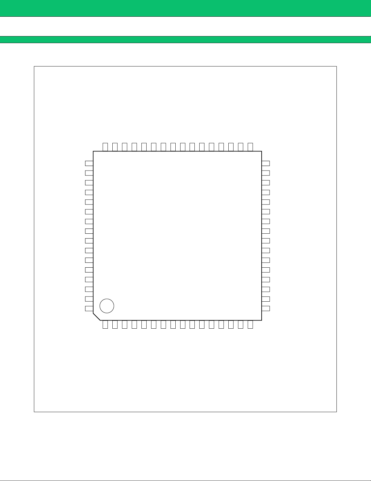
PACKAGE
■■■■
64-pin plastic LQFP
(FPT-64P-M03)
Page 2
MB3891
PIN ASSIGNMENT
■■■■
48 : SW3-INPUT
47 : SW3-OUTPUT
46 : SW1-INPUT
(TOP VIEW)
45 : SW1-OUTPUT
44 : CONT4
43 : VBAT4
42 : VBAT4
41 : OUT4
40 : OUT4
39 : GND4
38 : SIM-IO
37 : CLK
36 : RST
35 : µP-IO
34 : CLK-IN
33 : RESET-IN
N.C. : 49
N.C. : 50
SW2-OUTPUT : 51
SW2-INPUT : 52
SW1-ON : 53
SW2-ON : 54
SW3-ON : 55
CONT3 : 56
CONT5 : 57
OUT5 : 58
GND5 : 59
VBAT3 : 60
VBAT3 : 61
VBAT3 : 62
N.C. : 63
N.C. : 64
32 : GND-VSIM
31 : VCAP−
30 : VCAP+
29 : VSIMOUT
28 : OSC
27 : SIMPROG
26 : VSIM-ON
25 : VCC-VSIM
24 : REF-OUT
23 : VFIL
22 : VREF
21 : V-BACKUP
20 : VBAT2
19 : GND1
18 : DELAYCAP
17 : XPOWERGOOD
N.C. : 1
N.C. : 2
OUT3 : 3
OUT3 : 4
OUT2 : 6
GND3 : 5
OUT2 : 7
VBAT1 : 8
VBAT1 : 9
VBAT1 : 10
VBAT1 : 11
OUT1 : 12
OUT1 : 13
CONT1 : 14
CONT6 : 15
CONT2 : 16
(FPT-64P-M03)
2
Page 3
MB3891
PIN DESCRIPTION
■■■■
Pin No. Symbol I/O Descriptions
1, 2 N.C. Non connection.
3, 4 OUT3 O LDO3 output pin.
5GND3 LDO3 ground pin.
6, 7 OUT2 O LDO2 output pin.
8, 9, 10, 11 VBAT1 Battery voltage input pin for LDO1 and LDO2.
12, 13 OUT1 O LDO1 output pin.
14 CONT1 I Power on input from keypad (Active low, Pulled up to VBAT2).
15 CONT6 I “CONT6” input from digital system µP (Active high).
16 CONT2 I External accessory supply voltage Enable (Active high).
17 XPOWERGOOD O Generates the main reset. (Active low, when OUT1 is out of regulation).
18 DELAYCAP Timing capacitor for XPOWERGOOD delay.
19 GND1 LDO1, LDO2, V-BACKUP, Reference and System ground pin.
20 VBAT2
21 V-BACKUP O Supply voltage for Charger for rechargeable Lithium coin cell.
22 VREF O Supply voltage for Reference.
23 VFIL O Reference voltage Filter.
24 REF-OUT O Reference output voltage (Present when BACKUP UVLO is high).
25 VCC-VSIM Input voltage for charge pump. (Supplied by VBAT1).
26 VSIM-ON I VSIM supply Enable (Active high).
27 SIMPROG I VSIM programming: Low = 3 V SIM, High = 5 V SIM.
28 OSC Oscillator output pin.
29 VSIMOUT O Supply voltage for 3 or 5 V SIM-Card (SmartCard).
30 VCAP+Positive side of boost capacitor.
31 VCAP−Negative side of boost capacitor.
32 GND-VSIM 3 or 5 V SIM-Card (SmartCard) ground pin.
33 RESET-IN I Non level shifted SIM reset (µP side).
34 CLK-IN I Non level shifted clock (µP side).
35 µP-IO I/O Non level shifted bi-directional data input/output (µP side).
36 RST O Level shifted SIM reset (SmartCard side).
37 CLK O Level shifted SIM clock (SmartCard side).
Battery voltage input pin for both UVLO’s, Reference and V-BACKUP
LDO.
38 SIM-IO I/O Level shifted bi-directional SIM data input/output (SmartCard side).
39 GND4 LDO4 ground pin.
40, 41 OUT4 O LDO4 output pin.
(Continued)
3
Page 4
MB3891
(Continued)
Pin No. Symbol I/O Descriptions
42, 43 VBAT4 Supply voltage for LDO4.
44 CONT4 I OUT4 output voltage selection (“L”=2.8 V,“H”=2.5 V).
45 SW1-OUTPUT O Output of general purpose switch number 1 (Drain).
46 SW1-INPUT I Input of general purpose switch number 1 (Source).
47 SW3-OUTPUT O Output of general purpose switch number 3 (Drain).
48 SW3-INPUT I Input of general purpose switch number 3 (Source).
49, 50 N.C. Non connection.
51 SW2-OUTPUT O Output of general purpose switch number 2 (Drain).
52 SW2-INPUT I Input of general purpose switch number 2 (Source).
53 SW1-ON I General purpose switch number 1 Enable (Active high).
54 SW2-ON I General purpose switch number 2 Enable (Active high).
55 SW3-ON I General purpose switch number 3 Enable (Active high).
56 CONT3 I OUT3 and OUT4 supply voltage Enable (Active high).
57 CONT5 I OUT5 supply voltage Enable (Active high).
58 OUT5 O Output terminal of LDO5.
59 GND5 LDO5 ground pin.
60, 61, 62 VBAT3 Supply voltage for LDO and LDO5.
63, 64 N.C. Non connection.
4
Page 5
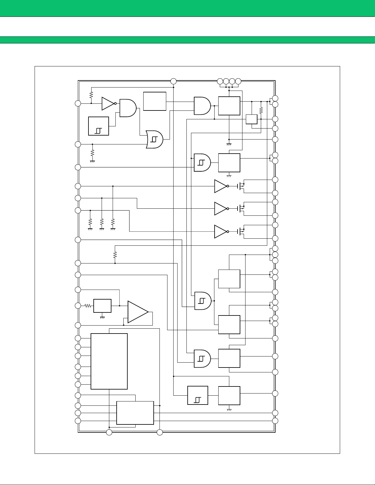
BLOCK DIAGRAM
■■■■
VBAT2 VBAT1
20
8 9 10 11
MB3891
CONT1
CONT6
CONT2
SW1-ON
SW2-ON
SW3-ON
CONT3
CONT5
CONT4
14
15
16
53
54
55
56
57
44
Main
UVLO
Over
Temp
Protection
SW1
SW2
SW3
LDO1
ON
LDO2
ON
LDO3
ON
OUT
OUT
OUT
POR
12
OUT1
13
XPOWERGOOD
17
DELAYCAP
18
GND1
19
6
OUT2
7
SW1-INPUT
46
SW1-OUTPUT
45
52
SW2-INPUT
51
SW2-OUTPUT
48
SW3-INPUT
47
SW3-OUTPUT
60
61
VBAT3
62
3
OUT3
4
VREF
VFIL
REF-OUT
RESET-IN
CLK-IN
µP-IO
RST
CLK
SIM-IO
VCC-VSIM
VSIM-ON
SIMPROG
OSC
22
23
24
33
34
35
36
37
38
25
26
27
28
VREF
GSM/SIM
Logic
Level
Translation
32
GND-VSIM
VREF-AMP
+
−
VSIMOUT
Charge-pump
29
VSIMOUT
BACKUP
UVLO
LDO4
OUT
ON
CONT4
LDO5
OUT
ON
LDO6
OUT
ON
N.C.
Pin : 1, 2, 49, 50, 63, 64
5
GND3
42
VBAT4
43
40
OUT4
41
GND4
39
58
OUT5
59
GND5
V-BACKUP
21
30
VCAP+
31
VCAP−
5
Page 6
MB3891
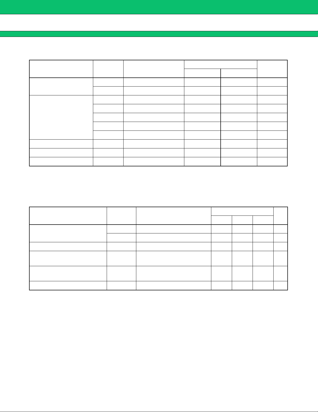
ABSOLUTE MAXIMUM RATINGS
■■■■
Parameter Symbol Conditions
Unit
Min. Max.
VBAT −0.3 7 V
Power supply voltage
VCC-VSIM −0.3 7 V
Rating
I
O OUT1 pin 120 mA
IO OUT2 pin 50 mA
LDO regulator
I
O OUT3 pin 100 mA
I
O OUT4 pin 100 mA
IO OUT5 pin 50 mA
VSIMOUT chargepump I
Power dissipation P
O VSIMOUT pin 10 mA
D Ta ≤ +25 °C 800* mW
Storage temperature Tstg −55 +125 °C
* : The packages are mounted on the dual-sided epoxy board(10 cm × 10 cm)
WARNING: Semiconductor devices can be permanently damaged by application of stress (voltage, current,
temperature, etc.) in excess of absolute maximum ratings. Do not exceed these ratings.
RECOMMENDED OPERATING CONDITIONS
■■■■
Value
Parameter Symbol Conditions
Min. Typ. Max.
Unit
Power supply voltage
VBAT 3.0 3.6 5.5 V
VCC-VSIM 3.0 3.6 5.5 V
LDO capacitor guarantee value C
REF-OUT capacitor guarantee
value
VSIMOUT capacitor guarantee
value
O OUT1 to OUT5, V-BACKUP pin 0.8 1.0 µF
CO REF-OUT pin 0.027 µF
C
O VSIMOUT pin 10 µF
Operating ambient temperature Ta −20 +25 +85 °C
WARNING: The recommended operating conditions are required in order to ensure the normal operation of the
semiconductor device. All of the device’s electrical characteristics are warranted when the device is
operated within these ranges.
Always use semiconductor devices within their recommended operating condition ranges. Operation
outside these ranges may adversely affect reliability and could result in device failure.
No warranty is made with respect to uses, operating conditions, or combinations not represented on
the data sheet. Users considering application outside the listed conditions are advised to contact their
FUJITSU representatives beforehand.
6
Page 7
ELECTRICAL CHARACTERISTICS
■■■■
Parameter Symbol Pin No. Conditions
MB3891
(Ta = +25 °C, VBAT1 to VBAT4 = VCC-VSIM = 3.6 V)
Value
Unit
Min. Typ. Max.
General
Shutdown supply
current
Standby supply
current
Operating ground
current
UVLO threshold
voltage
BACKUP UVLO
threshold voltage
I
BAT1
I
BAT2
I
BAT3
I
GND
8, 9, 10, 11,
20, 42, 43,
60, 61, 62
8, 9, 10, 11,
20, 42, 43,
60, 61, 62
8, 9, 10, 11,
20, 42, 43,
60, 61, 62
4, 5, 19,
32, 59
UVLO = “L”,
BACKUP UVLO = “L”
UVLO = “L”,
BACKUP UVLO = “H”
All circuit’s = On
(No load)
All circuit’s -VSIM =
On Max. load on all
regulators
80 µA
160 µA
400 µA
10 mA
8, 9, 10, 11,
THH
V
20, 42, 43,
OUT1 = ON 2.980 3.080 3.180 V
60, 61, 62
8, 9, 10, 11,
V
THL
20, 42, 43,
OUT1 = OFF 2.780 2.880 2.980 V
60, 61, 62
8, 9, 10, 11,
V
THH
20, 42, 43,
V-BACKUP = ON 2.980 3.080 3.180 V
60, 61, 62
8, 9, 10, 11,
V
THL
20, 42, 43,
V-BACKUP = OFF 2.580 2.680 2.780 V
60, 61, 62
V
IH 16, 56, 57
0.7 ×
OUT1
VIL 16, 56, 57 0
OUT1 V
0.3 ×
OUT1
V
Input voltage
Pull-up resistor
Pull-down resistor RPD 15, 53, 54, 55 200* kΩ
* : Standard design value
V
IH 14, 15, 44
V
IL 14, 15, 44 0
VIH 26, 27
V
IL 26, 27 0
R
PU 17 15* kΩ
R
PU 14, 57 200* kΩ
0.7 ×
VBAT
0.7 ×
VCC-VSIM
VBAT V
0.3 ×
VBAT
VCC-VSIM
0.3 ×
VCC-VSIM
(Continued)
V
V
V
7
Page 8
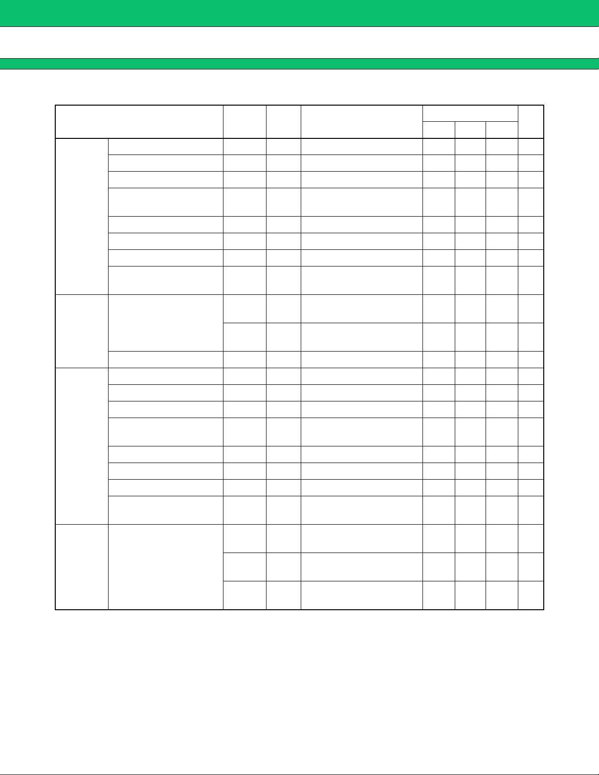
MB3891
Parameter Symbol
Output voltage V
Line regulation Line 12, 13 3.1 V < VBAT1 < 5.5 V 10 mV
Load reguration Load 12, 13 −50 µA > OUT1 > −120 mA 30 mV
(Ta = +25 °C, VBAT1 to VBAT4 = VCC-VSIM = 3.6 V)
Pin
No.
O 12, 13 −50 µA > OUT1 > −120 mA 2.000 2.100 2.200 V
Conditions
Value
Unit
Min. Typ. Max.
LDO1
(OUT1)
XPOWER-
GOOD
(RESET)
LDO2
(OUT2)
Ripple rejection
∆VBAT1/∆OUT1
Dropout voltage V
GND current at low load I
GND current at max. load I
Output noise volt. (RMS) VNOVL 12, 13
R.R 12, 13 f = 217 Hz 45 dB
DO 12, 13 OUT1 = −120 mA 500 mV
GND 19 OUT1 > −1 mA 30 µA
GND 19 OUT1 = −120 mA 2mA
f = 10 Hz to 1 MHz,
OUT1 = 1 µF
V
OH 17
500 µV
0.8 ×
OUT1
OUT1 V
Output voltage
V
OL 17 0
0.1 ×
OUT1
V
Hold time TXPG 17 DELAYCAP = 0.033 µF102540ms
Output voltage V
O 6, 7 −50 µA > OUT2 > −50 mA 2.700 2.800 2.900 V
Line regulation Line 6, 7 3.1 V < VBAT1 < 5.5 V 10 mV
Load regulation Load 6, 7 −50 µA > OUT2 > −50 mA 30 mV
Ripple rejection
∆VBAT1/∆OUT2
Dropout voltage V
GND current at low load I
R.R 6, 7 f = 217 Hz 45 dB
DO 6, 7 OUT2 = −50 mA 250 mV
GND 19 OUT2 > −1 mA 30 µA
GND current at max. load IGND 19 OUT2 = −50 mA 1mA
8
General
purpose
switches
Output noise volt. (RMS) V
Input/Output resistance
NOVL 6, 7
R
SW1 45, 46
RSW2 51, 52
R
SW3 47, 48
f = 10 Hz to 1 MHz,
OUT2 = 1 µF
SW1-INPUT = 2.8 V
(Gate/Source = 2.8 V)
SW2-INPUT = 2.8 V
(Gate/Source = 2.8 V)
SW3-INPUT = 2.8 V
(Gate/Source = 2.8 V)
350 µV
4.0 Ω
7.0 Ω
7.0 Ω
(Continued)
Page 9
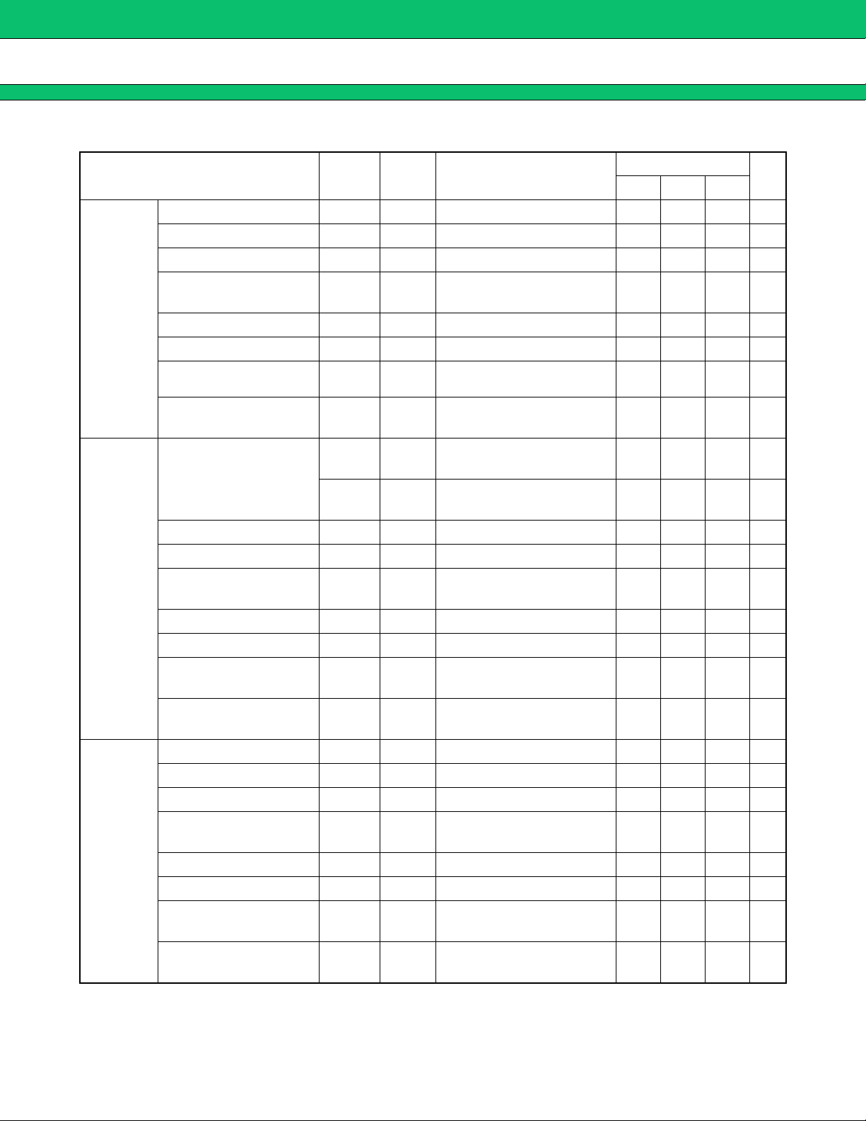
MB3891
(Ta = +25 °C, VBAT1 to VBAT4 = VCC-VSIM = 3.6 V)
Parameter Symbol Pin No. Conditions
Output voltage V
O 3, 4 −50 µA > OUT3 > −100 mA 2.700 2.800 2.900 V
Line regulation Line 3, 4 3.1 V < VBAT3 < 5.5 V 10 mV
Load regulation Load 3, 4 −50 µA > OUT3 > −100 mA 30 mV
Value
Unit
Min. Typ. Max.
LDO3
(OUT3)
LDO4
(OUT4)
Ripple rejection
∆VBAT3/∆OUT3
Dropout voltage V
GND current at low load I
GND current at max.
load
Output noise volt. (RMS) V
R.R 3, 4 f = 217 Hz 45 dB
DO 3, 4 OUT3 = −100 mA 250 mV
GND 5OUT3 > −1 mA 30 µA
I
GND 5OUT3 = −100 mA 2mA
NOVL 3, 4
V
O 40, 41
f = 10 Hz to 1 MHz,
OUT3 = 1 µF
−50 µA > OUT4 > −100 mA,
CONT4 = “L”
350 µV
2.700 2.800 2.900 V
Output voltage
VO 40, 41
−50 µA > OUT4 > −100 mA,
CONT4 = “H”
2.400 2.500 2.600 V
Line regulation Line 40, 41 3.1 V < VBAT4 < 5.5 V 10 mV
Load regulation Load 40, 41 −50 µA > OUT4 > −100 mA 30 mV
Ripple rejection
∆VBAT4 - OUT4/∆OUT4
Dropout voltage V
GND current at low load I
GND current at max.
load
Output noise volt. (RMS) VNOVL 40, 41
R.R 40, 41 f = 217 Hz 45 dB
DO 40, 41 OUT4 = −100 mA 250 mV
GND 39 OUT4 > −1 mA 30 µA
I
GND 39 OUT4 = −100 mA 2mA
f = 10 Hz to 1 MHz,
OUT4 = 1 µF
500 µV
LDO5
(OUT5)
Output voltage V
O 58 −50 µA > OUT5 > −50 mA 2.700 2.800 2.900 V
Line regulation Line 58 3.1 V < VBAT3 < 5.5 V 10 mV
Load regulation Load 58 −50 µA > OUT5 > −50 mA 30 mV
Ripple rejection
∆VBAT3/∆OUT5
Dropout voltage V
GND current at low load I
GND current at max.
load
Output noise volt. (RMS) V
R.R 58 f = 217 Hz 45 dB
DO 58 OUT5 = −50 mA 250 mV
GND 59 OUT5 > −500 µA 20 µA
IGND 59 OUT5 = −50 mA 1mA
NOVL 58
f = 10 Hz to 1 MHz,
OUT5 = 1 µF
350 µV
(Continued)
9
Page 10

MB3891
Parameter Symbol Pin No. Conditions
Output voltage V
Line regulation Line 21 3.1 V < VBAT2 < 5.5 V 10 mV
O 21
(Ta = +25 °C, VBAT1 to VBAT4 = VCC-VSIM = 3.6 V)
Value
Min. Typ. Max.
−10 µA > V-BACKUP
> −250 µA
2.000 2.100 2.200 V
Unit
LDO6
(V-BACKUP)
REF-OUT
Load regulation Load 21
−10 µA > V-BACKUP
> −250 µA
30 mV
Ripple rejection
∆VBAT2/
R.R 21 f = 217 Hz 25 dB
∆V-BACKUP
GND current at
low load
GND current at
max. load
Output noise volt.
(RMS)
Reverse current IRC 21
Output voltage V
I
GND 19 V-BACKUP > −10 µA 10 µA
I
GND 19 V-BACKUP = −250 µA 50 µA
V
NOVL 21
O 24 0 µA > REF-OUT > −50 µA 1.200 1.225 1.250 V
f = 10 Hz to 1 MHz,
V-BACKUP = 1 µF
VBAT2 = 0 V,
V-BACKUP = 3.0 V
500 µV
100 nA
Line regulation Line 24 3.1 V < VBAT2 < 5.5 V 10 mV
Load regulation Load 24 0 µA > REF-OUT > −50 µA 6mV
Ripple rejection
∆VBAT2/
R.R 24 f = 217 Hz 50 dB
∆REF-OUT
Output noise volt.
(RMS)
V
NOVL 24
f = 10 Hz to 1 MHz,
REF-OUT = 27 nF
250 µV
VSIMOUT
chargepump
10
O 29
V
−50 µA > VSIMOUT > −10 mA,
SIMPROG = “H”
4.600 5.000 5.400 V
Output voltage
VO 29
−50 µA > VSIMOUT > −10 mA,
SIMPROG = “L”
2.760 3.000 3.240 V
Line regulation Line 29 3.1 V < VCC-VSIM < 5.5 V 50 mV
Load regulation Load 29 −50 µA > VSIMOUT > −10 mA 100 mV
(Continued)
Page 11

(Ta = +25 °C, VBAT1 to VBAT4 = VCC-VSIM = 3.6 V)
Parameter Symbol Pin No. Conditions
Ripple rejection
∆VCC-VSIM/
R.R 29 f = 217 Hz 30 dB
∆VSIMOUT
MB3891
Value
Unit
Min. Typ. Max.
VSIMOUT
chargepump
GSM/SIM
logic level
translation
µp interface
Output current
GND current at
no load
Efficiency at
max. load
Output ripple
voltage
Shutdown supply current
Input voltage
Output voltage
I
O 29
I
O 29
3.1 V < VCC-VSIM < 5.5 V,
VSIMOUT = 5 V
3.1 V < VCC-VSIM < 5.5 V,
VSIMOUT = 3 V
10 mA
6 mA
IGND 32 VSIMOUT > −50 µA 100 µA
η 25, 29
V
RP 29
VSIMOUT = −10 mA,
VSIMOUT = 5 V
f = 10 Hz to 1 MHz,
VSIMOUT = 10 µF
85 %
100
mV
ILDO 25 VSIM-ON = “L” 100 nA
V
V
V
33, 34,
IH
IL
OH 35 µP-IO (max.) = −20 µA
35
33, 34,
35
0
VOL 35 µP-IO (max.) = 1 mA 0
0.7 ×
OUT1
0.8 ×
OUT1
OUT1 V
0.3 ×
OUT1
OUT1 V
0.2 ×
OUT1
V
V
(Continued)
PP
11
Page 12

MB3891
(Continued)
Parameter Symbol Pin No. Conditions
(Ta = +25 °C, VBAT1 to VBAT4 = VCC-VSIM = 3.6 V)
Value
Unit
Min. Typ. Max.
SIM
interface
5 V
(SIMPROG
= H)
Output voltage
V
V
Rise time T
OH 36 RST (max.) = −20 µA
OL 36 RST (max.) = 200 µA0 0.6 V
R 36 RESET-IN = RST = 30 pF 400 µs
VSIMOUT
− 0.7
VSIMOUT
V
Fall time TF 36 RESET-IN = RST = 30 pF 400 µs
0.7 ×
VSIMOUT
VSIMOUT V
Output voltage
OH 37 CLK (max.) = −20 µA
V
V
OL 37 CLK (max.) = 200 µA0 0.5 V
Rise time TR 37 CLK-IN = CLK = 30 pF 27 ns
Fall time T
F 37 CLK-IN = CLK = 30 pF 27 ns
OH 38 SIM-IO (max.) = −20 µA3.8 VSIMOUT V
V
Output voltage
VOL 38 SIM-IO (max.) = 1 mA 0 0.4 V
0.7 ×
VSIMOUT
VSIMOUT V
Input voltage
IH 38
V
V
IL 38 0 0.8 V
Rise time TR 38 SIM-IO = 30 pF 1 µs
Fall time T
F 38 SIM-IO = 30 pF 1 µs
V
OH 36 RST (max.) = −20 µA
0.8 ×
VSIMOUT
VSIMOUT V
Output voltage
V
OL 36 RST (max.) = 200 µA0
0.2 ×
VSIMOUT
V
Rise time TR 36 RESET-IN = RST = 30 pF 400 µs
(SIMPROG
12
SIM
interface
3 V
= L)
Fall time T
F 36 RESET-IN = RST = 30 pF 400 µs
OH 37 CLK (max.) = −20 µA
V
0.7 ×
VSIMOUT
VSIMOUT V
Output voltage
VOL 37 CLK (max.) = 200 µA0
Rise time T
Fall time T
VOH 38 SIM-IO (max.) = −20 µA
Output voltage
V
R 37 CLK-IN = CLK = 30 pF 50 ns
F 37 CLK-IN = CLK = 30 pF 50 ns
0.7 ×
VSIMOUT
OL 38 SIM-IO (max.) = 1 mA 0 0.4 V
IH 38
V
0.7 ×
VSIMOUT
VSIMOUT V
VSIMOUT V
0.2 ×
VSIMOUT
V
Input voltage
V
IL 38 0
0.2 ×
VSIMOUT
V
Rise time TR 38 SIM-IO = 30 pF 1 µs
Fall time T
F 38 SIM-IO = 30 pF 1 µs
Page 13

TYPICAL CHARACTERISTICS
■■■■
Power supply current vs. power supply voltage Power supply current vs. power supply voltage
MB3891
400
Ta = +25 °C
CONT1 = “L”
350
CONT2 = “H”
CONT3 = “H”
300
CONT4 = OPEN
CONT5 = OPEN
250
CONT6 = OPEN
VSIM-ON = “H”
200
SIMPROG = “H”
150
100
50
0
012
Power supply current IBAT (µA)
V-BACKUP = No load
VSIMOUT = No load
345
Power supply voltage V
Power supply current , GND current vs.
power supply voltage
450
400
350
300
250
200
150
100
50
0
Power supply current IBAT (mA)
Ta = +25 °C
CONT1 = OPEN
CONT2 = “H”
CONT3 = “H”
CONT4 = OPEN
CONT5 = OPEN
CONT6 = “H”
VSIM-ON = “H”
SIMPROG = “H”
0
12345
IBAT
V-BACKUP = 8.4 kΩ
VSIMOUT = 510 Ω
Power supply voltage VBAT (V)
350
Ta = +25 °C
CONT1 = OPEN
300
CONT2 = “H”
BAT (µA)
OUT1 = No load
OUT2 = No load
OUT3 = No load
OUT4 = No load
OUT5 = No load
Power supply current I
BAT (V) Power supply voltage VBAT (V)
CONT3 = “H”
250
CONT4 = OPEN
CONT5 = OPEN
CONT6 = “H”
200
VSIM-ON = “H”
SIMPROG = “H”
150
100
50
0
012345
V-BACKUP = No load
VSIMOUT = No load
Output voltage vs. power supply
voltage (LDO1)
3.0
)
2.5
OUT1 (V
2.0
1.5
1.0
0.5
Output voltage V
0.0
01234567
Ta = +25 °C
OUT1 = 1 µF
CONT1 = OPEN
CONT6 =
IGND
OUT1 = 18 Ω
OUT2 = 56 Ω
OUT3 = 28 Ω
OUT4 = 28 Ω
OUT5 = 56 Ω
450
400
350
300
250
200
150
100
50
0
GND current IGND (µA)
Power supply voltage VBAT (V)
OUT1 = No load
OUT2 = No load
OUT3 = No load
OUT4 = No load
OUT5 = No load
“H”
Output voltage vs. power supply voltage (LDO1)
3.0
Ta = +25 °C
OUT1 = 1 µF
2.5
CONT1 =
CONT6 = OPEN
2.0
1.5
1.0
0.5
“L”
Output voltage VOUT1 (V)
0.0
012345
Power supply voltage V
BAT (V)
Output voltage vs. load current (LDO1)
2.2
2.1
2.0
1.9
Ta = +25 °C
1.8
Output voltage VOUT1 (V)
1.7
0 −100 −200 −300 −500−400 −600 −700 −800
Load current I
VBAT = 3.6 V
CONT1 =
CONT6 = OPEN
LOAD (mA)
“L”
(Continued)
13
Page 14

MB3891
Ripple rejection vs. frequency (LDO1) Ripple rejection vs. frequency (LDO1)
0
−20
−40
−60
−80
Ripple rejection R.R (dBm)
−100
10 100 1 k 10 k 100 k 1 M
Frequency f (Hz) Frequency f (Hz)
Dropout voltage vs. load current (LDO1)
0.6
VBAT = 2.1 V
CONT1 = OPEN
0.5
CONT6 =
0.4
0.3
0.2
0.1
“H”
Dropout voltage VDO (V)
0.0
0 −50 −100 −150 −200
Load current ILOAD (mA)
Ta = +25 °C
VBAT = 3.6 V
OUT1 = 1 µF
OUT1 = 18 Ω
CONT1 =
CONT6 = OPEN
Ta = +85 °C
Ta = +25 °C
“L”
Ta = −20 °C
0
Ta = +25 °C
VBAT = 3.6 V
−20
OUT1 = 1 µF
CONT1 =
CONT6 = OPEN
−40
−60
−80
Ripple rejection R.R (dBm)
−100
10 100 1 k 10 k 100 k 1 M
“L”
Output voltage vs. ambient temperature (LDO1)
2.13
2.12
2.11
2.10
2.09
VBAT = 3.6 V
CONT1 = OPEN
CONT6 =
Output voltage VOUT1 (V)
2.08
−40 −20 0 20 40 60 80 100
Ambient temperature Ta ( °C)
“H”
14
Output voltage rising waveforms (LDO1)
10
5
0
VBAT
OUT1
Power supply voltage VBAT
Ta = +25°C
OUT1 = 18 Ω
CONT1 =
CONT6 = OPEN
0.0 0.5 1.0
1.5
2.0
3.0 3.5 4.0 4.5 5.0
2.5
t (ms)
“L”
2.0
1.5
1.0
0.5
0.0
Output voltage VOUT1 (V)
Page 15

MB3891
Output voltage falling waveforms (LDO1)
BAT (V)
4
3
2
1
0
Power supply voltage V
0 50 100 150 200 250 300
Ta = +25°C
OUT1 = No load
CONT1 = “L”
CONT6 = OPEN
VBAT
OUT1
350
t (ms)
Output voltage rising waveforms (LDO1)
4
2
0
CONT1
OUT1
Input voltage VCONT1 (V)
Ta = +25°C
VBAT = 3.6 V
OUT1 = 18 Ω
CONT6 = OPEN
020406080 100 120 140 160 180
t (µs)
400 450 500
200
2
1
0
Output voltage VOUT1 (V)
2
1
0
Output voltage VOUT1 (V)
Output voltage falling waveforms (LDO1)
Ta = +25°C
VBAT
OUT1
VBAT = 1 µF
OUT1 = No load
CONT1 =
CONT6 = OPEN
4
2
0
Power supply voltage VBAT (V)
0.0 0.2 0.4 0.6 0.8 1.0 1.2 1.4 1.6 1.8
t (s)
Output voltage falling waveforms (LDO1)
10
5
CONT1 (V)
0
CONT1
Ta = +25°C
VBAT = 3.6 V
OUT1 = No load
CONT6 = OPEN
Input voltage V
OUT1
0
20 40 60 80
100 120 140 160 180 200
t (ms)
“L”
2.0
OUT1 (V)
2
1
0
Output voltage V
2.0
OUT1 (V)
1.5
1.0
0.5
0.0
Output voltage V
Waveform at rapid change of output load
(LDO1)
2.0
1.5
1.0
0.5
0.0
Ta = +25°C
VBAT = 3.6 V
CONT1 =
CONT6 = OPEN
Output voltage VOUT1 (V)
OUT1 = 0 A −120 mA
01020304050
60
70
t (µs)
OUT1
VC
80
“L”
90 100
[Measurement diagram]
VBAT = 3.6 V
VREF = 1.225 V
(IC internal)
2
1
0
NPN collector voltage VC (V)
LDO1
OUT1
1 µF
120 mA
VC
4 V
0 V
(Continued)
15
Page 16

MB3891
Waveform at rapid change of output load (LDO1)
2.0
1.5
1.0
0.5
0.0
Output voltage VOUT1 (V)
0.0 0.5
OUT1 = −120 mA 0 A
1.5 2.0 2.5
1.0
OUT1
VC
Ta = +25°C
VBAT = 3.6 V
CONT1 = “L”
CONT6 = OPEN
3.5 4.0 4.5
3.0
5.0
t (ms)
Waveform at rapid change of output load (LDO2)
3.0
2.5
2.0
1.5
1.0
0.5
Output voltage VOUT2 (V)
0.0
OUT2 = 0 A −50 mA
0 102030405060708090100
OUT2
Ta = +25°C
VBAT = 3.6 V
CONT1 =
CONT2 = “H”
CONT6 = OPEN
“L”
V
C
t (µs)
[Measurement diagram]
VREF = 1.225 V
(IC internal)
2
1
0
NPN Collector voltage VC (V)
[Measurement diagram]
VREF = 1.225 V
(IC internal)
3
2
1
0
NPN Collector voltage VC (V)
VBAT = 3.6 V
LDO1
VBAT = 3.6 V
LDO2
OUT1
1 µF
OUT2
1 µF
120 mA
VC
4 V
0 V
50 mA
VC
4 V
0 V
16
Waveform at rapid change of output load (LDO2)
3.0
2.5
2.0
1.5
1.0
0.5
Output voltage VOUT2 (V)
0.0
OUT2 = −50 mA 0 A
0 102030405060708090100
OUT2
VC
Ta = +25°C
VBAT = 3.6 V
CONT1 =
CONT2 = “H”
CONT6 = OPEN
“L”
t (ms)
[Measurement diagram]
VREF = 1.225 V
(IC internal)
3
2
1
0
NPN Collector voltage VC (V)
VBAT = 3.6 V
LDO2
OUT2
1 µF
50 mA
VC
4 V
0 V
(Continued)
Page 17

MB3891
Reference voltage vs. power supply voltage Reference voltage vs. ambient temperature
1.4
1.2
1.0
0.8
0.6
0.4
0.2
Reference voltage VFIL (V)
0.0
01234567
Power supply voltage V
Ta = +25 °C
VFIL = 0.1 µF
BAT (V) Ambient temperature Ta ( °C)
Power supply current vs. power supply voltage
(VSIMOUT Chargepump)
Power supply current ICC-VSIM (µA)
100000
10000
1000
100
10
1
012
Power supply voltage VCC-VSIM (V)
VSIMOUT = 510 Ω
VSIMOUT = No load
Ta = +25 °C
VBAT = 3.6 V
VSIM-ON =
SIMPROG = “H”
345
“H”
1.24
1.23
FIL (V)
1.22
1.21
1.20
1.19
Reference voltage V
−40 −20 0
20 40 60 80 100
VBAT = 3.6 V
Power supply current vs. power supply voltage
(VSIMOUT Chargepump)
100000
VSIMOUT = 510 Ω
VSIMOUT = No load
Ta = +25 °C
VBAT = 3.6 V
VSIM-ON =
SIMPROG = “L”
345
Power supply current ICC-VSIM (µA)
10000
1000
100
10
1
012
Power supply voltage VCC-VSIM (V)
“H”
Output voltage vs. power supply voltage
(VSIMOUT Chargepump)
5
SIMPROG = “H”
4
3
2
1
VSIMOUT = No load
SIMPROG = “L”
VSIMOUT = No load
Output voltage VSIMOUT (V)
0
012
34567
Power supply voltage V
Ta = +25 °C
VBAT = 3.6 V
VSIM-ON =
CC-VSIM (V)
“H”
(Continued)
17
Page 18

MB3891
Output voltage vs. load current
(VSIMOUT Chargepump)
3.00
2.99
2.98
2.97
2.96
2.95
2.94
2.93
2.92
2.91
Output voltage VSIMOUT (V)
2.90
VCC-VISM = 5.5 V
VCC-VISM = 3.1 V
0 −5 −10 −15
Load current I
Ripple rejection vs. frequency
(VSIMOUT Chargepump)
0
−20
−40
Output voltage vs. load current
(VSIMOUT Chargepump)
Ta = +25 °C
VSIM-ON = “H”
SIMPROG = “L”
VCC-VISM = 3.6 V
−20
LOAD (mA) Load current ILOAD (mA)
5.00
Ta = +25 °C
4.95
VSIM-ON = “H”
SIMPROG = “H”
4.90
SIMOUT (V)
4.85
4.80
4.75
4.70
4.65
Output voltage V
4.60
VCC-VISM = 3.1 V
0 −5 −10 −15
VCC-VISM = 5.5 V
VCC-VISM
= 3.6 V
Ripple rejection vs. frequency
(VSIMOUT Chargepump)
0
Ta = +25 °C
VBAT = VCC-VSIM = 3.6 V
−20
−40
VSIM-ON = “H”
SIMPROG = “H”
VCAP+ VCAP− = 0.1 µF
VSIMOUT = 10 µF
−20
−60
−80
Ripple rejection R.R (dBm)
−100
10 100 1 k
Ta = +25 °C
VBAT = VCC-VSIM = 3.6 V
VSIM-ON = “H”
SIMPROG = “H”
VCAP+ VCAP− = 0.1 µF
VSIMOUT = 10 µF
VSIMOUT = 510 Ω
10 k 100 k 1 M
Frequency f (Hz)
Ripple rejection vs. frequency
(VSIMOUT Chargepump)
0
−20
−40
−60
−80
Ripple rejection R.R (dBm)
−100
10 100 1 k 10 k 100 k 1 M
Ta = +25 °C
VBAT = VCC-VSIM = 3.6 V
VSIM-ON =
SIMPROG = “L”
VCAP+ VCAP− = 0.1 µF
VSIMOUT = 10 µF
VSIMOUT = 510 Ω
Frequency f (Hz)
“H”
−60
−80
Ripple rejection R.R (dBm)
−100
10 100 1 k
10 k 100 k 1 M
Frequency f (Hz)
Ripple rejection vs. frequency
(VSIMOUT Chargepump)
0
Ta = +25 °C
VBAT = VCC-VSIM = 3.6 V
−20
−30
−40
−80
Ripple rejection R.R (dBm)
−100
VSIM-ON = “H”
SIMPROG = “L”
VCAP+ VCAP− = 0.1 µF
VSIMOUT = 10 µF
10 100 1 k 10 k 100 k 1 M
Frequency f (Hz)
18
(Continued)
Page 19

MB3891
Efficiency vs. power supply voltage
(VSIMOUT Chargepump)
100
90
80
70
60
50
40
30
Efficiency η (%)
20
10
0
3.0 3.5 4.0
Power supply voltage V
Efficiency vs. load current
(VSIMOUT Chargepump)
100
90
80
70
60
50
40
30
Efficiency η (%)
20
10
0
0 −5 −10
VCC-VSIM = 5.5 V
VCC-VSIM = 3.1 V
Ta = +25 °C
VSIM-ON =
SIMPROG = “L”
ILOAD = −10 mA
ILOAD = −1 mA
4.5 5.0 5.5
CC-VSIM (V) Power supply voltage VCC-VSIM (V)
Ta = +25 °C
VBAT = VCC-VSIM = 3.6 V
VSIM-ON =
SIMPROG = “L”
“H”
VCC-VSIM = 3.6 V
−15 −20
Load current ILOAD (mA)
“H”
Efficiency vs. power supply voltage
100
90
80
70
60
50
Efficiency η (%)
100
Efficiency η (%)
40
30
20
10
0
90
80
70
60
50
40
30
20
10
0
ILOAD = −1 mA
3.0 3.5 4.0
VCC-VSIM = 3.1 V
VCC-VSIM = 3.6 V
0 −5 −10
(VSIMOUT Chargepump)
Ta = +25 °C
VSIM-ON = “H”
SIMPROG = “H”
ILOAD = −10 mA
4.5 5.0 5.5
Efficiency vs. load current
(VSIMOUT Chargepump)
VCC-VSIM = 5.5 V
Ta = +25 °C
VBAT = VCC-VSIM = 3.6 V
VSIM-ON =
SIMPROG = “H”
“H”
−15 −20
Load current ILOAD (mA)
Output voltage rising waveforms
(VSIMOUT Chargepump)
10
5
0
Input voltage VSIM-ON (V)
Ta = +25 °C
VBAT = VCC-VSIM = 3.6 V
SIMPROG =
VSIMOUT = 510 Ω
0.0 0.5 1.5 2.0 2.5 3.0 3.5
t (ms)
VSIM-ON
VSIMOUT
“H”
4.0
Output voltage rising waveforms
(VSIMOUT Chargepump)
10
5
Output voltage VSIMOUT (V)
0
Input voltage VSIM-ON (V)
Ta = +25 °C
VBAT = VCC-VSIM = 3.6 V
SIMPROG =
VSIMOUT = 510 Ω
0.0 0.5 1.5 2.0 2.5 3.0 3.5 4.0 4.5 5.01.0
5
4
3
2
1
0
4.5 5.01.0
VSIM-ON
VSIMOUT
“L”
SIMOUT (V)
3
2
1
0
Output voltage V
t (ms)
(Continued)
19
Page 20

MB3891
10
5
0
Input voltage VSIMPROG (V)
10
5
0
Input voltage VSIM-ON (V)
Output voltage rising waveforms
(VSIMOUT Chargepump)
SIMPROG
VSIMOUT
Ta = +25 °C
VBAT = VCC-VSIM = 3.6 V
VSIMOUT = 510 Ω
VSIM-ON =
0.0 0.5 1.5 2.0 2.5 3.0 3.5 4.0 4.5 5.01.0
t (ms)
Output voltage falling waveforms
(VSIMOUT Chargepump)
Ta = +25 °C
VBAT = VCC-VSIM = 3.6 V
SIMPROG =
VSIMOUT = 510 Ω
VSIM-ON
VSIMOUT
“H”
“H”
5
4
3
2
1
0
Output voltage VSIMOUT (V)
SIM-ON (V)
5
4
3
Input voltage V
2
1
0
Output voltage VSIMOUT (V)
10
5
0
Input voltage VSIMPROG (V)
0.0 0.5 1.5 2.0 2.5 3.0 3.5 4.0 4.5 5.01.0
10
5
0
Output voltage falling waveforms
(VSIMOUT Chargepump)
SIMPROG
VSIMOUT
Ta = +25 °C
VBAT = VCC-SIM = 3.6 V
VSIMOUT = 510 Ω
VSIM-ON =
“H”
t (ms)
Output voltage falling waveforms
(VSIMOUT Chargepump)
Ta = +25 °C
VBAT = VCC-VSIM = 3.6 V
SIMPROG = “L”
VSIMOUT = 510 Ω
VSIM-ON
VSIMOUT
5
IMOUT (V)
4
3
2
1
0
Output voltage VS
SIMOUT (V)
3
2
1
0
Output voltage V
20
40
20
0
−20
−40
Output voltage VSIMOUT (mV)
0 5 15 20 25 30 35 40 45 5010
Output voltage waveforms
(VSIMOUT Chargepump)
Ta = +25 °C
VBAT = VCC-VSIM = 3.6 V
VSIM-ON = “H”
SIMPROG = “H”
VSIMOUT = No load
AC COUPLED
0 2 6 8 10 12 14 16 18 204
t (ms)
t (µs)
20
0
−20
Output voltage VSIMOUT (mV)
0 5 15 20 25 30 35 40 45 5010
Output voltage waveforms
(VSIMOUT Chargepump)
Ta = +25 °C
VBAT = VCC-SIM = 3.6 V
VSIM-ON =
SIMPROG = “L”
VSIMOUT = No load
AC COUPLED
0 2 6 8 10 12 14 16 18 204
“H”
t (ms)
t (µs)
(Continued)
Page 21

MB3891
40
20
0
−20
−40
Output voltage VSIMOUT (mV)
40
20
0
−20
−40
Output voltage VSIMOUT (mV)
Output voltage waveforms
(VSIMOUT Chargepump)
Ta = +25 °C
VBAT = VCC-VSIM = 3.6 V
VSIM-ON =
SIMPROG = “L”
VSIMOUT = 510 Ω
AC COUPLED
0246810
t (µs)
Output voltage waveforms
(VSIMOUT Chargepump)
Ta = +25 °C
VBAT = VCC-VSIM = 3.6 V
VSIM-ON = “H”
SIMPROG = “H”
VSIMOUT = 510 Ω
AC COUPLED
12
“H”
14 16
18 20
20
0
−20
Output voltage VSIMOUT (mV)
0246
60
40
20
0
−20
−40
−60
Output voltage VSIMOUT (mV)
Output voltage waveforms
(VSIMOUT Chargepump)
Ta = +25 °C
VBAT = VCC-VSIM = 3.6 V
VSIM-ON = “H”
SIMPROG = “L”
VSIMOUT = 5.1 kΩ
AC COUPLED
81012
14 16
t (µs)
Output voltage waveforms
(VSIMOUT Chargepump)
Ta = +25 °C
VBAT = VCC-VSIM = 3.6 V
VSIM-ON =
SIMPROG = “H”
VSIMOUT = 5.1 kΩ
AC COUPLED
“H”
18
20
0 2 4 6 8 101214161820
t (µs)
Output voltage vs. input voltage (SIM Inter-
5
4
3
2
1
Output voltage VSIMIO (V)
0
0.0 0.5 1.0
SIMPROG = "H"
SIMPROG = "L"
Ta = +25 °C
VBAT = VCC-VSIM = 3.6 V
VSIM-ON = "H"
CONT1 = "L"
CONT6 = OPEN
1.5 2.0 2.5
Input voltage VUPIO (V)
0 2 4 6 8 101214161820
t (µs)
Output voltage vs. input voltage (SIM Interface)
2.5
2.0
1.5
1.0
0.5
Output voltage VUPIO (V)
0.0
012
Ta = +25 °C
VBAT = VCC-VSIM = 3.6 V
VSIM-ON = “H”
SIMPROG = “L” or “H”
CONT1 = “L”
CONT6 = OPEN
345
Input voltage VSIMIO (V)
(Continued)
21
Page 22

MB3891
(Continued)
Output voltage vs. ambient temperature
(SIM Interface)
3.10
3.05
3.00
2.95
2.90
2.85
2.80
Output voltage VSIMOUT (V)
−40 −20 0
VBAT = VCC-VSIM = 3.6 V
VSIM-ON = “H”
SIMPROG = “L”
20 40 60 80 100
Ambient temperature Ta ( °C)
Power dissipation vs. ambient temperature
1000
800
600
Output voltage vs. ambient temperature
(SIM Interface)
5.00
4.95
4.90
4.85
4.80
4.75
4.70
Output voltage VSIMOUT (V)
−40 −20 0
VBAT = VCC-VSIM = 3.6 V
VSIM-ON = “H”
SIMPROG = “H”
20 40 60 80 100
Ambient temperature Ta ( °C)
400
200
Power dissipation PD (mW)
0
−40 −20 200
Ambient temperature Ta ( °C)
40 60 80 100
22
Page 23

MB3891
FUNCTIONAL DESCRIPTION
■■■■
(1) MAIN UVLO/BACKUP UVLO
Transient power-on surge states or sudden drops in supply voltage (VBAT2) can cause an IC to operate abnormally , leading to destruction or damage to system elements. To prevent this type of fault, the undervoltage loc kout
circuits (UVLO/ Backup UVLO) will shut off the output from OUT1 to V-BACKUP if the supply voltage f alls belo w
the UVLO circuit threshold voltage (3.0 V/2.8 V typ .). System operation is restored as soon as the supply voltage
rises above the UVLO circuits threshold voltage (3.2 V typ.).
(2) LDO1
The LDO1 circuits uses the reference voltage supply and generates an output voltage (2.1 V typ.) at the OUT1
terminal (pin 12,13). Power can be dr awn from the OUT1 terminal for external use, up to a maximum load current
of 120 mA.
(3) XPOWERGOOD (RESET)
When the OUT1 terminal (pin 12,13) voltage exceeds 2.0 V (typ.), after a delay interval set by a capacitor
(C
DELAY CAP) connected to the DELAYCAP terminal (pin 18), the XPOWERGOOD terminal (pin 17) goes to “H”
level and resets the microcomputer. At the same time, the LDO2, LDO3, and LDO4 output is controlled ON/OFF.
(4) LDO2
The LDO2 circuit uses the reference voltage supply and generates an output voltage (2.8 V typ.) at the OUT2
terminal (pin 6,7) when the XPOWERGOOD terminal (pin 17) voltage is at “H” level and an “H” level signal is
input at the CONT2 terminal (pin 16). Power can be drawn from the OUT2 ter minal for external use, up to a
maximum load current of 50 mA.
(5) General Purpose switches
Any of the OUT terminals can be connected to any SW-INPUT terminal so that when the corresponding SWON terminal is at “H” level, the OUT terminal voltage can be dra wn from the associated SW-OUTPUT terminal.
(6) LDO3
The LDO3 circuits uses the reference voltage supply and generates an output voltage (2.8 V typ.) at the OUT3
terminal (pin 3,4) when the XPOWERGOOD terminal (pin 17) voltage is at “H” level and an “H” level signal is
input at the CONT3 terminal (pin 56). Power can be drawn from the OUT3 ter minal for external use, up to a
maximum load current of 100 mA.
(7) LDO4
The LDO4 circuits uses the reference voltage supply and generates an output voltage (2.8 V typ.) at the OUT4
terminal (pin 40,41) when the XPOWERGOOD terminal (pin 17) voltage is at “H” lev el and an “H” le v el signal is
input at the CONT3 terminal (pin 56) , and an “L” level signal is input at the CONT4 terminal (pin 44). When an
“H” level signal is input at the CONT4 terminal, the output voltage at the OUT4 terminal is 2.5 V (typ.). Power
can be drawn from the OUT4 terminal for external use, up to a maximum load current of 100 mA.
23
Page 24

MB3891
(8) LDO5
The LDO5 circuits uses the reference voltage supply and generates an output voltage (2.8 V typ.) at the OUT5
terminal (pin 57) when the OUT1 terminal (pin 12,13) is in output state and an “H” level signal is input at the
CONT5 terminal (pin 57). Power can be dr awn from the OUT5 terminal for external use, up to a maximum load
current of 50 mA.
(9) LDO6
The LDO6 circuit uses the reference voltage supply and gener ates an output voltage (2.1 V typ.) at the V -BACKUP
terminal (pin 21). Power can be drawn for external use, from the V-BACKUP terminal, up to a maximum load
current of 250 µA.
(10) REF-OUT
This circuit uses the reference voltage generated by the reference voltage block (1.225 V typ.) to produce a
temperature compensated reference voltage (1.225 V typ.) at the REF-OUT terminal(pin 24) by means of a
voltage follower. The reference voltage can also be drawn from the REF-OUT terminal for external use, up to a
load current of 50 µA.
(11) VSIMOUT Chargepump
The VSIMOUT charge pump uses the voltage from the battery and generates 5.0 V (typ.) v oltage at the VSIMOUT
terminal (pin 29) when an “H” level signal is input at the SIMPROG terminal (pin 27) , or 3.0 V (typ.) voltage
when an “L” level signal input at the SIMPROG ter minal. This voltage can also be drawn from the VSIMOUT
terminal for external use, up to a load current of 10 mA.
(12) GSM/SIM Logic Translation µP Interface
When a signal is input from the microprocessor to the RESET-IN terminal(pin 33) and CLK-IN terminal (pin 34),
a level-shifted voltage is output from the RST terminal (pin 36) and CLK terminal (pin 37) to the SIM card. The
µP-IO terminal (pin 35) and SIM-IO terminal (pin 38) are input/output pins and carr y signals between the
microprocessor and SIM card.
(13) SIM Interface 5 V (SIMPROG = “H”)
When an “H” level signal is input to the SIMPROG ter minal (pin 27), 5.0 V (typ.) voltage is generated from the
VSIMOUT terminal (pin 29) as a power supply for the SIM card.
(14) SIM Interface 3 V (SIMPROG = “L”)
When an “L” level signal is input to the SIMPROG ter minal (pin 27), 3.0 V (typ.) voltage is generated from the
VSIMOUT terminal (pin 29) as a power supply for the SIM card.
SETTING THE XPOWERGOOD TIME
■■■■
When the OUT1 terminal (pin 12,13) voltage exceeds 2.0 V (typ.), the capacitor (CDELAYCAP) connected to the
DELAYCAP terminal (pin 18) starts charging, the XPOWERGOOD terminal (pin 17) voltage rises. The XPOWERGOOD terminal voltage rising time (XPOWERGOOD time) can be set by a capacitor connected to the
DELAYCAP terminal.
XPOWERGOOD time : T
24
XPG (s) := 0.8 × CDELAYCAP (µF)
Page 25

OPERATION TIMING CHART
■■■■
Input
VBAT1 to VBAT4,
VCC-VSIM
CONT1
CONT6
CONT5
CONT2
CONT3
SW1-ON
SW2-ON (SW3-ON)
MB3891
Output
VSIM-ON
SIMPROG
REF-OUT
OUT6
OUT1
XPOWERGOOD
OUT5
OUT2
OUT3 (OUT4)
SW1-OUTPUT
SW2-OUTPUT
(SW3-OUTPUT)
VSIMOUT
2.0 V
delay
VSIMOUT = 3 V
VSIMOUT = 5 V
(1) (2) (3) (4) (5) (6) (7) (8) (9) (10) (11) (12) (13) (14) (15) (16) (17)
(1) : Battery controlled (5) : OUT1 hold
(2) : BACKUP UVLO ON (6) to (12) : µP controlled
(3) : phone turned on (14) : Main UVLO off
(4) : XPOWERGOOD on (16) : BACKUP UVLO off
25
Page 26

MB3891
APPLICATION EXAMPLE
■■■■
µP
KEYPAD
C8
0.1 µF
R1
200 kΩ
R2
200 kΩ
R3
200 kΩ
R4
200 kΩ
R5
200 kΩ
14
CONT1
CONT6
15
CONT2
16
SW1-ON
53
54
SW2-ON
SW3-ON
55
56
CONT3
CONT5
57
CONT4
44
VREF
22
VFIL
23
REF-OUT
24
26
VSIM-ON
27
SIMPROG
33
RESET-IN
34
CLK-IN
35
µP-IO
20
VBAT2
C12
1 µF
8 9 10 11
VBAT1
XPOWERGOOD
DELAYCAP
SW2-INPUT
SW2-OUTPUT
SW3-INPUT
SW3-OUTPUT
SW1-INPUT
OUT1
GND1
OUT2
VBAT3
OUT3
GND3
12
13
17
18
19
52
51
48
47
60
61
62
46
C11
1 µF
C1
1 µF
C2
0.033 µF
6
7
3
4
5
C3
1 µF
C13
1 µF
C4
1 µF
26
SIM
C9
10 µF
C10
0.1 µF
VCC-VSIM
25
OSC
28
29
VSIMOUT
30
VCAP+
VCAP−
31
36
RST
CLK
37
38
SIM-IO
32
GND-VSIM
SW1-OUTPUT
OUT5
GND5
VBAT4
OUT4
GND4
V-BACKUP
45
58
59
42
43
40
41
39
21
C5
1 µF
C14
1 µF
C6
1 µF
C7
1 µF
N.C.
Pin : 1, 2, 49, 50, 63, 64
Page 27

MB3891
USAGE PRECAUTIONS
■■■■
• Printed circuit board ground lines should be set up with consideration for common impedance.
•Take appropriate static electricity measures.
• Containers for semiconductor materials should hav e anti-static protection or be made of conductive material.
• After mounting, printed circuit boards should be stored and shipped in conductive bags or Containers.
• Work platforms, tools, and instruments should be properly grounded.
• Working personal should be grounded with resistance of 250 kΩ to 1 MΩ between body and ground.
• Do not apply negative voltages
The use of negative voltages belo w -0.3V may create parasitic transistors on LSI lines, Which can cause abnormal
operation.
ORDERING INFORMATION
■■■■
Part number Package Remarks
MB3891PFV
64-pin Plastic LQFP
(FPT-64P-M03)
27
Page 28

MB3891
PACKAGE DIMENSION
■■■■
64-pin plastic LQFP
(FPT-64P-M03)
12.00±0.20(.472±.008)SQ
10.00±0.10(.394±.004)SQ
48
49
64
LEAD No.
0.50±0.08
(.020±.003)
INDEX
33
161
+0.08
–0.03
0.18
+.003
.007 –.001
Note : Pins width and pins thickness include plating thickness.
32
0.08(.003)
Details of "A" part
+0.20
1.50
–0.10
(Mounting height)
+.008
.059
17
0.08(.003)
"A"
M
0.145±0.055
(.006±.002)
–.004
0~8°
0.50±0.20
(.020±.008)
0.45/0.75
(.018/.030)
0.10±0.10
(.004±.004)
(Stand off)
0.25(.010)
C
1998 FUJITSU LIMITED F64009S-3C-6
Dimensions in mm (inches) .
Page 29

MB3891
FUJITSU LIMITED
All Rights Reserved.
The contents of this document are subject to change without notice.
Customers are advised to consult with FUJITSU sales
representatives before ordering.
The information and circuit diagrams in this document are
presented as examples of semiconductor device applications, and
are not intended to be incorporated in devices for actual use. Also,
FUJITSU is unable to assume responsibility for infringement of
any patent rights or other rights of third parties arising from the use
of this information or circuit diagrams.
The products described in this document are designed, developed
and manufactured as contemplated for general use, including
without limitation, ordinary industrial use, general office use,
personal use, and household use, but are not designed, developed
and manufactured as contemplated (1) for use accompanying fatal
risks or dangers that, unless extremely high safety is secured, could
have a serious effect to the public, and could lead directly to death,
personal injury, severe physical damage or other loss (i.e., nuclear
reaction control in nuclear facility, aircraft flight control, air traffic
control, mass transport control, medical life support system, missile
launch control in weapon system), or (2) for use requiring
extremely high reliability (i.e., submersible repeater and artificial
satellite).
Please note that Fujitsu will not be liable against you and/or any
third party for any claims or damages arising in connection with
above-mentioned uses of the products.
Any semiconductor devices have an inherent chance of failure. You
must protect against injury, damage or loss from such failures by
incorporating safety design measures into your facility and
equipment such as redundancy, fire protection, and prevention of
over-current levels and other abnormal operating conditions.
If any products described in this document represent goods or
technologies subject to certain restrictions on export under the
Foreign Exchange and Foreign Trade Law of Japan, the prior
authorization by Japanese government will be required for export
of those products from Japan.
F0007
FUJITSU LIMITED Printed in Japan
 Loading...