

Page 1

查询MB3874供应商
FUJITSU SEMICONDUCTOR
DATA SHEET
ASSP
For Po wer Supply Applications (Lithium ion battery charger)
DS04-27704-2E
DC/DC Con verter IC f or Parallel Char ging
MB3874/MB3876
DESCRIPTION
■
The MB3874 and MB3876 are parallel charging DC/DC converter ICs suitable f or do wn-con version, which uses
pulse width modulation (PWM) for controlling the output voltage and current independently.
These ICs can dynamically control the secondary batter y’s charge current by detecting a voltage drop in an AC
adapter in order to keep its power constant (dynamically-controlled charging).
The charging method enables quick charging, f or example, with the A C adapter during operation of a notebook PC.
The IC also enable parallel charging, or charging two batteries at the same time, dramatically reducing the charging
time.
With an on-chip output voltage setting resistor which allows the output voltage to be set at high precision, these
ICs are best suited as internal battery chargers for notebook PCs.
The MB3874 support 3-cell battery and the MB3876 support 4-cell battery.
FEATURES
■
• Detecting a voltage drop in the AC adapter and dynamically controlling the charge current (Dynamically-controlled charging)
• High efficiency : 93 %(In rev erse-current preventive diode)
• Wide range of operating supply voltages : 7 V to 25 V
• Output voltage precision
(Built-in output voltage setting resistor ) : ± 0.8 % (Ta = + 25 °C)
• High precision reference voltage source : 4.2 V ± 0.8 %
(Continued)
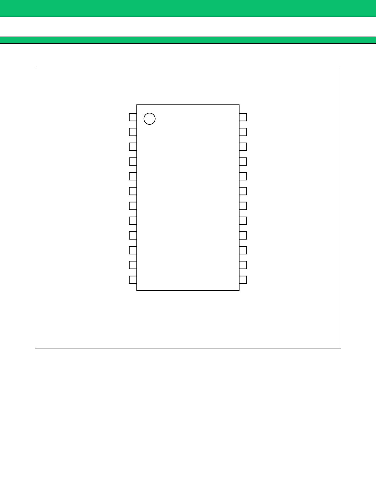
PACKAGE
■
24-pin plastic SSOP
(FPT-24P-M03)
Page 2

MB3874/MB3876
(Continued)
• Support for frequency setting using an external resistor
(Frequency setting capacitor integrated) :100 kHz to 500 kHz
• Built-in current detector amplifier with wide in-phase input voltage range : 0 V to V
• Built-in standby current function : 0 µA (Typ.)
• Built-in soft start function
• Capable of parallel charging (Charging the two battery packs at a time)
• Internal totem-pole output stage supporting P-channel MOS FETs devices
CC
2
Page 3
PIN ASSIGNMENT
■
−INC1 :
FB2 :
−INE2 :
+INE2 :
MB3874/MB3876
(TOP VIEW)
: +INC1
1
2
3
4
24
23
22
21
: GND
: CS
: V
CC
VREF :
CTL :
FB1 :
−INE1 :
+INE3 :
−INE3 :
FB3 :
−INC2 :
10
11
12
5
6
7
8
9
20
19
18
17
16
15
14
13
: OUT
: VH
: OUTM
: RT
: −INE4
: FB4
: −INE5
: +INC2
(FPT-24P-M03)
3
Page 4

MB3874/MB3876
PIN DESCRIPTION
■
Pin No. Symbol I/O Descriptions
1 –INC1 I Output voltage feedback input pin.
2 FB2 O Error amplifier (Error Amp. 2) output pin.
3 –INE2 I Error amplifier (Error Amp. 2) inverted input pin.
4+INE2 I
5 VREF O Reference voltage output pin.
6CTL I
7 FB1 O Error amplifier (Error Amp. 1) output pin.
8–INE1 I
9+INE3 I
10 –INE3 I Error amplifier (Error Amp. 3) inverted input pin.
11 FB3 O Error amplifier (Error Amp. 3) output pin.
12 –INC2 I Output voltage feedback input pin.
13 +INC2 I Current detection amplifier (Current Amp. 2) input pin .
14 –INE5 I Error amplifier (Error Amp. 5) inverted input pin.
15 FB4 O Error amplifier (Error Amp. 4, 5) output pin.
16 –INE4 I Error amplifier (Error Amp. 4) inverted input pin.
17 RT — Triangular-wave oscillation frequency setting resistor connection pin.
18 OUTM O
Error amplifier (Error Amp. 2) non-inverted input pin.
Input pin for charge current setting voltage
Power supply control pin.
Setting the CTL pin low places the IC in the standby mode.
Error amplifier (Error Amp. 1) inverted input pin
Input pin for dynamically-controlled charging voltage setting
Error amplifier (Error Amp. 3) non-inverted input pin.
Input pin for charge current setting voltage
Output pin for dynamically controlled charging identification signal
“H” level: Constant-voltage or constant-current charging mode
“L” level: Dynamically controlled charging mode
19 VH O Power supply pin for FET drive circuit (VH = Vcc − 5 V).
20 OUT O High-side FET gate drive pin.
21 V
22 CS — Soft-start capacitor connection pin.
23 GND — Ground pin.
24 +INC1 I Current detection amplifier (Current Amp. 1) input pin .
4
CC — Power supply pin for reference power supply and control circuit.
Page 5
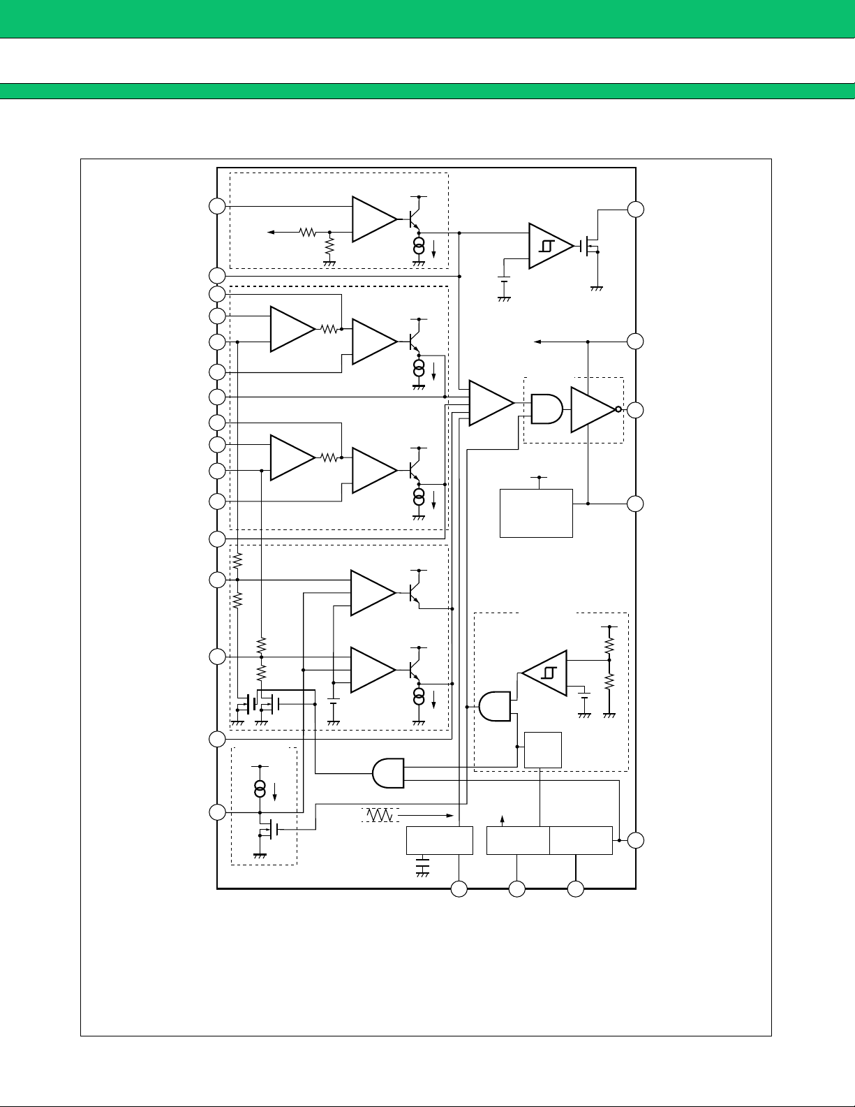
BLOCK DIAGRAM
■
MB3874/MB3876
−INE1
FB1
−INE2
+INC1
−INC1
+INE2
FB2
−INE3
+INC2
−INC2
+INE3
FB3
−INE4
−INE5
FB4
8
V
7
3
<Current Amp.1>
24
1
4
2
10
<Current Amp.2>
13
12
9
11
R1
∗
16
R2
50 kΩ
14
15
<SOFT>
VREF
CC
+
× 25
−
+
× 25
−
R1
∗
R2
50 kΩ
1 µA
208 kΩ
100 kΩ
100 kΩ
<Error Amp.1>
−
+
42 kΩ
<Error
Amp.2>
−
+
<Error
Amp.3>
−
+
<Error
Amp.4>
−
+
+
<Error
Amp.5>
−
+
+
VREF
(4.2 V)
VREF
VREF
VREF
VREF
VREF
<PWM
Comp.>
+
+
+
+
−
Bias voltage
block
(V
<MASK Comp.>
−
+
2.5 V
V
CC
<OUT>
V
CC
<VH>
<UVLO>
CC
UVLO)
215 kΩ
+
−
0.91 V
(0.77 V)
VREF
ULVO
Drive
(VCC − 5 V)
CC
V
35 kΩ
18
21
20
19
OUTM
CC
V
OUT
VH
CS
22
2.5 V
1.5 V
(45 pF)
bias
<OSC>
17 5 23
RT
<Ref> <CTL>
VREF
∗
:
CTL
6
GND
MB3874 100 kΩ
MB3876 150 kΩ
5
Page 6
MB3874/MB3876
ABSOLUTE MAXIMUM RATINGS
■
Parameter Symbol Conditions
Unit
Min. Max.
Rating
Power supply voltage V
Output terminal current I
Peak output current I
OUTM terminal output voltage V
Power dissipation P
CC ——28V
OUT ——60mA
OUT Duty ≤ 5% (t =1 / fOSC × Duty) — 500 mA
OUTM ——17V
D Ta ≤ +25°C — 740* mW
Storage temperature Tstg — –55 +125 °C
*: The package is mounted on the dual-sided epoxy board (10 cm × 10 cm).
WARNING: Semiconductor devices can be permanently damaged by application of stress (voltage, current,
temperature, etc.) in excess of absolute maximum ratings. Do not exceed these ratings.
RECOMMENDED OPERATING CONDITIONS
■
Value
Parameter Symbol Conditions
Unit
Min. Typ. Max.
Power supply voltage V
Reference voltage output
current
CC —7—25V
REF —–1—0mA
I
VH pin output current IVH —0—30mA
-INC –INC1, –INC2 0 — 17 V
V
Input voltage
CTL pin input voltage V
Output current I
Peak output current I
OUTM pin output voltage V
OUTM pin output current I
Oscillator frequency f
Timing resistor R
Soft-start capacitor C
VH pin capacitor C
Reference voltage output
capacitor
INE –INE1 to –INE5, +INE2 0 — VCC – 1.8 V
V
+INC +INC1, +INC2 0 — VCC V
V
CTL —0—25V
OUT OUT pin –45 — 45 mA
OUT Duty ≤ 5% (t =1 / fOSC × Duty) –450 — 450 mA
OUTM ——315V
OUTM ———1mA
OSC — 100 290 500 kHz
T — 33 47 130 kΩ
S — — 2200 100000 pF
VH ——0.11.0µF
REF ——0.11.0µF
C
Operating ambient temperature Ta — –30 +25 +85 °C
WARNING: The recommended operating conditions are required in order to ensure the normal operation of the
semiconductor device. All of the device’s electrical characteristics are warranted when the device is
operated within these ranges.
Always use semiconductor devices within their recommended operating condition ranges. Operation
outside these ranges may adversely affect reliability and could result in device failure.
No warranty is made with respect to uses, operating conditions, or combinations not represented on
the data sheet. Users considering application outside the listed conditions are advised to contact their
FUJITSU representatives beforehand.
6
Page 7
ELECTRICAL CHARACTERISTICS
■
Parameter
Symbol
Pin No. Conditions
MB3874/MB3876
(MB3874 : Ta = +25°C, VCC = 16 V, VREF = 0 mA)
(MB3876 : Ta = +25°C, V
Value
Min. Typ. Max.
CC = 19 V, VREF = 0 mA)
Unit Remarks
Output voltage V
Input stability Line 5 V
Load stability Load 5 VREF = 0 mA to –1 mA — 1 10 mV
block (Ref)
Short-circuit
Reference voltage
output current
Threshold
voltage
Hysteresis width V
Under voltage
Threshold
lockout protection
voltage
circuit block (UVLO)
Hysteresis width V
REF 5
Ta = –30°C to +85°C 4.158 4.200 4.242 V
Ta = +25°C 4.167 4.200 4.233 V
CC = 7 V to 25 V — 3 10 mV
I
OS 5 VREF = 1 V –25 –15 –5 mA
V
TLH
V
CC = 6.3 6.6 6.9 V
21
V
THL VCC = 5.3 5.6 5.9 V
H 21 — 0.7 1.0 1.3 V
V
TLH
VREF = 2.6 2.8 3.0 V
5
V
THL VREF= 2.4 2.6 2.8 V
H 5 — 0.05 0.20 0.35 V
Charge current ICS 22 — –1.3 –0.8 –0.5 µA
block
(SOFT)
Soft-start
Oscillation
frequency
Frequency tem-
block (OSC)
oscillator circuit
perature stability
Triangular waveform
*: Standard design value.
OSC
f
∆f/fdt
20
RT = 47 kΩ 260 290 320 kHz
20
Ta = –30°C to +85°C — 1* — %
(Continued)
7
Page 8

MB3874/MB3876
(Continued)
Parameter Symbol Pin No Conditions
(MB3874 : Ta = +25°C, VCC = 16 V, VREF = 0 mA)
(MB3876 : Ta = +25°C, V
CC = 19 V, VREF = 0 mA)
Value
Unit Remarks
Min. Typ. Max.
Threshold
voltage
Input pin current IIN
Voltage gain A
Frequency
bandwidth
(Error Amp.1)
Output voltage
Error amplifier block
Output source
current
Output sink
current
Input offset
voltage
Input pin
current
Common mode
input voltage
range
FB1 = 2 V,
–INE1 = 2.35 V
V
TH 21
FB1 = 2 V,
–INE1 = 2.83 V
8
–INE1= 0 V –100 –30 — nA
V 7 DC — 100* — dB
14.00 14.20 14.40 V
16.80 17.10 17.40 V
MB3874
MB3876
BW 7 AV = 0 dB — 2.0* — MHz
FBH 7—3.94.1—V
V
VFBL 7 — — 20 200 mV
I
SOURCE 7 FB1 = 2 V — –2.0 –0.6 mA
I
SINK 7 FB1 = 2 V 150 300 — µA
VIO
I
INE 4,9 +INE2 = +INE3 = 0 V –100 –30 — nA
V
CM
3,4
9,10
3,4
9,10
FB2 = FB3 = 2 V — 1* — mV
—0—VCC–1.8 V
Voltage gain A
Frequency
bandwidth
(Error Amp.2, 3)
Error amplifier block
Output voltage
Output source
current
Output sink
current
*: Standard design value.
8
V 2, 11 DC — 100* — dB
BW 2, 11 A
V = 0 dB — 2.0* — MHz
VFBH 2, 11 — 3.9 4.1 — V
V
FBL 2, 11 — — 20 200 mV
I
SOURCE 2, 11 FB2 = FB3 = 2 V — –2.0 –0.6 mA
ISINK 2, 11 FB2 = FB3 = 2 V 150 300 — µA
(Continued)
Page 9

(Continued)
Parameter Symbol Pin No Conditions
Threshold
voltage
Input current
Input resistor
(Current Amp.4, 5)
Error amplifier block
Voltage gain A
Frequency
bandwidth
MB3874/MB3876
(MB3874 : Ta = +25°C, VCC = 16 V, VREF = 0 mA)
(MB3876 : Ta = +25°C, V
Value
Min. Typ. Max.
12.500 12.600 12.700 V
16.666 16.800 16.934 V
12.474 12.600 12.726 V
16.632 16.800 16.968 V
V
TH 1, 12
FB4 = 2 V,
Ta = +25 °C
FB1 = 2 V,
Ta = –30 °C to +85 °C
–INC1 = –INC2 = 12.6 V — 84 150 µA
INEH 1, 12
I
–INC1 = –INC2 = 16.8 V — 84 150 µA
V
CC = 0 V,
–INC1 = –INC2 = 12.6 V
—0 1µA
IINEL 1, 12
VCC = 0 V,
–INC1 = –INC2 = 16.8 V
—0 1µA
70 100 130 kΩ
1 1, 12 —
R
105 150 195 kΩ
R2 14, 16 — 355065kΩ
V 15 DC — 100* — dB
BW 15 AV = 0 dB — 2.0* — MHz
CC = 19 V, VREF = 0 mA)
Unit Remarks
MB3874
MB3876
MB3874
MB3876
MB3874
MB3876
MB3874
MB3876
MB3874
MB3876
Output voltage
Output source
current
Output sink
current
*: Standard design value.
V
FBH 15 — 3.9 4.1 — V
V
FBL 15 — — 20 200 mV
I
SOURCE 15 FB4 = 2 V — –2.0 –0.6 mA
ISINK 15 FB4 = 2 V 150 300 — µA
(Continued)
9
Page 10

MB3874/MB3876
(Continued)
Parameter
Symbol
Pin No. Conditions
(MB3874 : Ta = +25°C, VCC = 16 V, VREF = 0 mA)
(MB3876 : Ta = +25°C, V
CC = 19 V, VREF = 0 mA)
Value
Unit Remarks
Min. Typ. Max.
I
+INCH 13, 24
Input current
I+INCL 13, 24
-INE1 3, 10
V
Current detection
voltage
V-INE2 3, 10
V-INE3 3, 10
(Current Amp.1, 2)
Common mode
Current detection amplifier block
input voltage range
Voltage gain A
V
-INE4 3, 10
V
CM
V 3, 10
1, 12,
13, 24
+INC1= +INC2=12.7 V,
–INC1= –INC2=12.6 V
+INC1= +INC2=16.9 V,
–INC1= –INC2=16.8 V
+INC1= +INC2= 0.1 V,
–INC1= –INC2= 0 V
+INC1= +INC2=12.7 V,
–INC1= –INC2=12.6 V
+INC1= +INC2=16.9 V,
–INC1= –INC2=16.8 V
+INC1= +INC2=12.63V,
–INC1= –INC2=12.6 V
+INC1= +INC2=16.83 V,
–INC1= –INC2=16.8 V
+INC1= +INC2= 0.1 V ,
–INC1= –INC2= 0 V
+INC1= +INC2= 0.03 V,
–INC1= –INC2= 0 V
—0—VCC V
+INC1= +INC2=12.7 V,
–INC1= –INC2=12.6 V
+INC1= +INC2=16.9 V,
–INC1= –INC2=16.8 V
—1020µA
—1020µA
–130 –65 — µA
2.25 2.50 2.75 V
2.25 2.50 2.75 V
0.50 0.75 1.00 V
0.50 0.75 1.00 V
1.25 2.50 3.75 V
0.125 0.750 1.375 V
22.5 25 27.5 V/V
22.5 25 27.5 V/V
MB3874
MB3876
MB3874
MB3876
MB3874
MB3876
MB3874
MB3876
Constant power
10
OUTCH 3, 10 — 3.9 4.1 — V
V
Output voltage
VOUTCL 3, 10 — — 20 200 mV
Threshold voltage
block
(PWM Comp.)
PWM comparator
VTL
TH
V
V
TLH 18 FB1 = 2.7 2.8 2.9 V
2, 7,
11, 15
2, 7,
11, 15
Duty cycle = 0 % 1.4 1.5 — V
Duty cycle = 100 % — 2.5 2.6 V
Threshold voltage
V
THL 18 FB1 = 2.4 2.5 2.6 V
Hysteresis width V
Output leak current I
detection block
(MASK Comp.)
H 18 — 0.2 0.3 0.4 V
LEAK 18 OUTM = 5 V — 0 1 µA
Output voltage VOL 18 OUTM = 1 mA — 0.15 0.4 V
(Continued)
Page 11

(Continued)
Parameter
Output source
current
Output sink current ISINK 20
(OUT)
Output block
Output ON resistor
Rise time tr1 20
Fall time tf1 20
CTL input voltage
MB3874/MB3876
(MB3874 : Ta = +25°C, VCC = 16 V, VREF = 0 mA)
(MB3876 : Ta = +25°C, V
Value
Symbol
Pin No. Conditions
Min. Typ. Max.
OUT = 11 V,
Duty ≤ 5 %
— –200* — mA
(t = 1/fosc × Duty )
I
SOURCE 20
OUT = 14 V,
Duty ≤ 5 %
— –200* — mA
(t = 1/fosc × Duty )
OUT = 16 V,
Duty ≤ 5 %
— 200* — mA
(t = 1/fosc × Duty )
OUT = 19 V,
Duty ≤ 5 %
— 200* — mA
(t = 1/fosc × Duty )
OH 20 OUT = −45 mA — 8.0 16.0 Ω
R
R
OL 20 OUT = 45 mA — 6.5 13.0 Ω
ON 6
V
V
OFF 6
OUT = 3300 pF
(Equivalent to Si4435DY)
OUT = 3300 pF
(Equivalent to Si4435DY)
Active mode
Standby mode
—70*—ns
—60*—ns
2.0 — 25.0 V
0—0.8V
CC = 19 V, VREF = 0 mA)
Unit Remarks
MB3874
MB3876
MB3874
MB3876
(CTL)
Input current
Control block
Output voltage VH 19
Bias
voltage
block (VH)
Standby current I
Power supply
current
General
*: Standard design value
I
CTLH 6
CTLL 6
I
CCS 21
CC 21
I
CTL = 5 V
CTL = 0 V
V
= 7 V to 25 V,
CC
VH = 0 to 30 mA
CTL = 0 V
CTL = 5 V
— 100 200 µA
—0 1µA
VCC –
5.5
VCC –
5.0
VCC –
4.5
V
—010µA
—6.09.0mA
—6.59.5mA
MB3874
MB3876
11
Page 12

MB3874/MB3876
TYPICAL CHARACTERISTICS
■
Power supply current vs. power supply voltage
10
8
6
4
2
Ta = +25 °C
CTL = 5 V
Power supply current ICC (mA)
0
0 5 10 15 20 25
Power supply voltage VCC (V)
Reference voltage vs. VREF load current
REF (V)
10
8
6
4
2
Ta = +25 °C
VCC = 16 V (MB3874)
VCC = 19 V (MB3876)
CTL = 5 V
Reference voltage V
0
0 5 10 15 20 25 30
Reference voltage vs. power supply voltage
10
8
6
4
2
Ta = +25 °C
CTL = 5 V
VREF = 0 mA
Reference voltage VREF (V)
0
0 5 10 15 20 25
Power supply voltage V
CC (V)
Reference voltage vs. ambient temperature
2.0
1.5
1.0
0.5
0.0
-0.5
-1.0
-1.5
Reference voltage ∆VREF (%)
-2.0
-40 -20 0 20 40 60 80 100
VCC = 16 V (MB3874)
VCC = 19 V (MB3876)
CTL = 5 V
VREF = 0 mA
12
VREF load current I
Reference voltage vs. CTL pin voltage
10
8
6
4
2
Ta = +25 °C
V
VCC = 19 V (MB3876)
VREF = 0 mA
Reference voltage VREF (V)
0
0 5 10 15 20 25
CTL pin voltage VCTL(V)
REF (mA)
CC = 16 V (MB3874)
Ambient temperature Ta (°C)
CTL pin current vs. CTL pin voltage
1.0
0.8
0.6
0.4
0.2
Ta = +25 °C
VCC = 16 V (MB3874)
VCC = 19 V (MB3876)
CTL pin current ICTL (µA)
0.0
0 5 10 15 20 25
CTL pin voltage V
CTL (V)
(Continued)
Page 13

(Continued)
MB3874/MB3876
Triangular wave oscillator frequency vs.
timing resistor
1 M
100 k
10 k
10 k 100 k 1 M
Triangular wave oscillator frequency fOSC(Hz)
Timing resistor RT (Ω)
Ta = +25 °C
V
CC = 16 V (MB3874)
VCC = 19 V (MB3876)
CTL = 5 V
Triangular wave oscillator frequency vs.
ambient temperature
350
340
330
320
310
300
290
280
270
260
250
−40 −20 0 20 40 60 80 100
Triangular wave oscillator frequency fOSC(kHz)
Ambient temperature Ta (°C)
VCC = 16 V (MB3874)
V
CC = 19 V (MB3876)
CTL = 5 V
RT = 47 kΩ
Triangular wave oscillator frequency vs.
power supply voltage
350
340
330
320
310
300
290
280
270
260
250
0 5 10 15 20 25
Triangular wave oscillator frequency fOSC(kHz)
Power supply voltage V
Ta = +25 °C
CTL = 5 V
RT = 47 kΩ
CC (V)
Error amplifier threshold voltage vs.
ambient temperature
5.0
4.0
3.0
VCC = 16 V (MB3874)
CC
= 19 V (MB3876)
V
CTL = 5 V
2.0
1.0
0.0
−1.0
−2.0
−3.0
−4.0
−5.0
Error amplifier threshold voltage ∆VTH(%)
−40 −20 0 20 40 60 80 100
Ambient temperature Ta (°C)
13
Page 14
MB3874/MB3876
(Continued)
Error amplifier gain and phase vs. frequency
AV
Ta = +25 °C
180
90
0
−90
−180
Phase φ (deg)
Gain AV (dB)
40
20
0
−20
−40
100 1 k 10 k 100 k 1 M 10 M
φ
Frequency f (Hz)
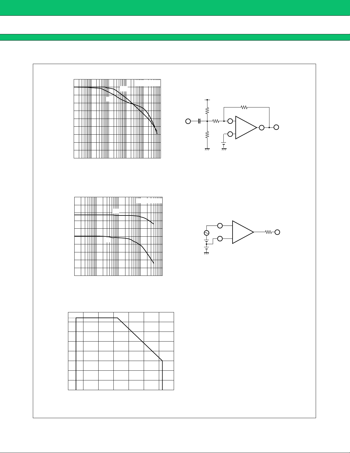
Current detection amplifier gain and phase vs. frequency
40
20
AV
0
φ
Ta = +25 °C
180
90
0
Gain AV (dB)
−20
−90
Phase φ (deg)
−40
−180
IN
1 µF
− +
IN
0.1 V
4.2 V
10 kΩ
2.4 kΩ
10 kΩ
∗
∗ :
MB3874 12.6 V
MB3876 16.8 V
VCC = 16 V (MB3874)
V
CC = 19 V (MB3876)
240 kΩ
3
−
(10)
+
4
(9)
2.088 V
CC = 16 V (MB3874)
V
V
CC = 19 V (MB3876)
24
1
+
× 25
−
Current Amp.1
(Current Amp.2)
(13)
(12)
2
(11)
Error Amp.2
(Error Amp.3)
100 kΩ
OUT
3
(10)
OUT
14
100 1 k 10 k 100 k 1 M
Frequency f (Hz)
Power dissipation vs. ambient temperature
800
740
700
600
500
400
300
200
100
Power dissipation PD (mW)
0
−40 −20 0 20 40 60 80 100
Ambient temperature Ta (°C)
Page 15

MB3874/MB3876
FUNCTIONAL DESCRIPTION
■
1. DC/DC Converter Unit
(1) Reference voltage block (Ref)
The reference voltage gener ator uses the v oltage supplied from the Vcc terminal (pin 21) to generate a temperature-compensated, stable voltage ( := 4.2 V) used as the reference supply voltage for the IC’s internal circuitry.
The reference voltage can be output, up to 1 mA, to an external device through the VREF terminal (pin 5).
(2) Triangular wave oscillator block (OSC)
The triangular wave oscillator generates a triangular waveform with a frequency setting resistor connected to
the internal frequency setting capacitor via the RT terminal (pin 17).
The triangular wave is input to the PWM comparator on the IC.
(3) Error amplifier block (Error Amp.1)
This error amplifier (Error Amp.1) detects a voltage drop in the AC adapter and outputs a PWM control signal
as well as a signal to the dynamically controlled charging detection block (MASK Comp.).
In addition, an arbitrary loop gain can be set by connecting a feedback resistor and capacitor from the FB1
terminal (pin 7) to the −INE1 terminal (pin 8) of the error amplifier, enabling stable phase compensation to the
system.
(4) Error amplifier block (Error Amp.2, 3)
These error amplifiers (Error Amp.2, Error Amp .3) detect the output signals from the current detector amplifiers
(Current Amp.1, Current Amp .2), compare them with the +INE2 terminal (pin 4) and +INE3 terminal (pin 9), and
output PWM control signals to control the charge current.
In addition, these amplifiers allow an arbitrary loop gain to be set by connecting a feedbac k resistor and capacitor
from the FB2 terminal (pin 2) to −INE2 terminal (pin 3) and from the FB3 terminal (pin 11) to −INE3 terminal (pin
10) of the error amplifiers, enabling stable phase compensation to the system.
(5) Error amplifier block (Error Amp.4, 5)
This error amplifier (Error Amp.4, Error Amp .5) detects the output voltage from the switching rerulator and outputs
the PWM control signal. The error amplifier inverted input pin is connected to the output voltage setting resistor
in the IC, eliminating the need f or an external resistor f or setting the output voltage. The MB3874 and MB3876
are set to output voltage of 12.6 V (for a 3-cell battery) and 16.8 V (for a 4-cell battery), respectively; these ICs
are suitable for use in equipment that uses a lithium-ion battery.
In addition, an arbitrary loop gain can be set by connecting a feedback resistor and capacitor from the FB4
terminal (pin 15) to the −INE4 terminal (pin 16) to the −INE5 ter minal (pin 14) of the error amplifier, enabling
stable phase compensation to the system.
Connecting a soft-start capacitor to the CS terminal (pin 22) prevents surge currents when the IC is turned on.
Using an error amplifier for soft start detection makes the soft start time constant, independent of the output load.
(6) Current detector amplifier block (Current Amp.1, 2)
The current detection amplifier (Current Amp.1, Current Amp.2) detects a voltage drop which occurs between
both ends of the output sense resistor (RS1) due to the flow of the charge current, using the +INC1 terminal
(pin 24) and
−INC1 terminal (pin 1). Then it outputs the signal amplified by 25 times to the error amplifier (Error Amp.2) at
the next stage.The amplifiers also detect a voltage drop which occurs at both ends of the output sense resistor
15
Page 16

MB3874/MB3876
(RS2) using the +INC2 terminal (pin 13) and −INC2 terminal (pin 12) and output the signal amplified by 25 times
to the error amplifier (Error Amp. 3) at the next stage.
(7) PWM comparator block (PWM Comp.)
The PWM comparator circuit is a voltage-pulse width conver ter for controlling the output duty of the error
amplifiers (Error Amp. 1 to Error Amp. 5) depending on their output voltage.
The PWM comparator circuit compares the triangular wave generated by the triangular wave oscillator to the
error amplifier output voltage and turns on the external output transistor during the interval in which the triangular
wave voltage is lower than the error amplifier output voltage.
(8) Output block (OUT)
The output circuit uses a totem-pole configuration capable of driving an external P-channel MOS FET.
The output “L” level sets the output amplitude to 5 V (typical) using the voltage generated by the bias voltage
block (VH).
This results in increasing conversion efficiency and suppressing the withstand v oltage of the connected external
transistor in a wide range of input voltages.
(9) Control block (CTL)
Setting the CTL terminal (pin 6) low places the IC in the standby mode. (The supply current is 10 µA at maximum
in the standby mode.)
(10) Bias voltage block (VH)
The bias voltage circuit outputs Vcc − 5 V (typical) as the minimum potential of the output circuit. In the standb y
mode, this circuit outputs the potential equal to Vcc.
2. Protection Functions
Low-Vcc malfunction preventive circuit (UVLO)
The transient state or a momentary decrease in supply voltage or internal reference voltage (VREF), which
occurs when the power supply is turned on, may cause malfunctions in the control IC, resulting in breakdown
or degradation of the system. To prevent such malfunction, the low-Vcc malfunction preventive circuit detects
a supply voltage or internal reference voltage drop and fixes the OUT terminal (pin 20) to the “H” level. The
system restores voltage supply when the supply voltage or internal reference voltage reaches the threshold
voltage of the low-Vcc malfunction preventive circuit.
3. Soft Start Function
Soft start block (SOFT)
Connecting a capacitor to the CS terminal (pin 22) prevents surge currents when the IC is turned on. Using an
error amplifier for soft start detection makes the soft start time constant, independent of the output load of the
DC/DC converter.
4. Additional Functions
Dynamically controlled charging detection block (MASK Comp.)
The dynamically controlled charging detection block (MASK Comp.) usually output the “H” level signal. The
OUTM signal becomes low (“L” level) when the output voltage of the error amplifier (Error Amp. 1) that detects
the input voltage (Vcc) becomes lower than the crest v alue (2.5 V) of the triangular wa veform generator (OSC).
The OUTM signal return high (“H” level) when the input voltage reaches 2.8 V or more.
16
Page 17

MB3874/MB3876
METHOD OF SETTING THE CHARGING CURRENT
■
The charge current (output control current) value can be set with the voltage at the +INE2, +INE3 terminal.
If a current exceeding the set value attempts to flo w , the charge v oltage drops according to the set current value.
Battery 1 charge current setting voltage : +INE2
+INE2 (V) = 25 × I1 (A) × R
S1 (Ω)
Battery 2 charge current setting voltage : +INE3
+INE3 (V) = 25 × I2 (A) × R
METHOD OF SETTING THE SOFT START TIME
■
S 2 (Ω)
Upon activation, the IC starts charging the capacitor (Cs) connected to the CS terminal .
The error amplifier causes soft start operation to be performed with the output voltage in proportion to the CS
pin voltage regardless of the load current of the DC/DC converter.
Soft start time ts (Time taken for the output voltage to reach 100 %)
ts (s) := 4.2 × C
METHOD OF SETTING THE TRIANGULAR W AVE OSCILLAT OR FREQUENCY SETTING
■
S (µF)
The trianguar wave oscillator frequency can be set b y the timing resistor (RT) connected the RT terminal (pin 17).
Triangular wave oscillator frequency fOSC
fOSC (kHz) := 14444 / RT (kΩ)
AC ADAPTER VOLTAGE DETECTION
■
When partial potential point A of the AC adapter voltage (Vcc) becomes lower than the voltage at the –INE1
pin, the IC enters the constant-power mode to reduce the charge current in order to keep AC adapter power
constant.
AC adapter detected voltage setting Vth
Vth (V) = (208k + 42k) / 42k × − INE1 := 5.95 × − INE1
− INE1 setting voltage range : 1.176 V to 4.2 V (equivalent to 7 V to 25 V for Vcc)
−INE1
8
VCC
A
208 kΩ
<Error Amp.1>
−
+
42 kΩ
17
Page 18

MB3874/MB3876
OPERATION TIMING DIAGRAM
■
2.8 V
2.5 V
Err Amp.2, 3
Err Amp.4, 5
Err Amp.1
OUT
OUTM
FB2,3
FB4
FB1
AC adapter dynamically-
controlled charging
Constant voltage
control
Constant current control
1.5 V
AC adapter dynamicallycontrolled charging
About the OUTM signal
The OUTM signal becomes low when the output voltage of the error amplifier (Error Amp. 1) that detects the
AC adapter voltage (Vcc) becomes lo wer than the crest value (2.5 V) of the triangular wav eform generator (OSC).
If the sum of the current consumption by the system and that by the charger e xceeds the current capacity of the
AC adapter, the IC detects a voltage drop in the AC adapter output and switches to the dynamically-controlled
charging mode from C.V.C.C (constant-voltage/constant-current charging control) mode.
In the dynamically-controlled charging mode, the OUTM pin outputs the L level signal to distinguish between
the case in which the charge current has become small as the system current consumption has increased and
the case in which it has become small as battery charging has been finished.
L: Dynamically-controlled charging
H: C.V.C.C (constant-voltage/constant-current charging control) or IC standby mode
Battery
V
IN
AC
Adaptor
Mode
Signal
Charger
MB3874
MB3876
Ichg
Battery
18
ISYS
System
Power
Page 19

MB3874/MB3876
NOTE ON AN EXTERNAL REVERSE-CURRENT PREVENTIVE DIODE
■
If there is an imbalance in charge current (I1, I2) under constant-voltage control, voltage is controled at the side
with a lower battery voltage and thus the battery voltage at one side is higher than that at the other by the voltage
difference between the re verse-current preventive diodes (D1, D2) and between the sense resistors (Rs
Pay attention to the voltage/current characteristics of the reverse-current preventive diode (D1, D2) not to let it
exceed the overcharge stop voltage.
VIN
(16 V/19 V)
to 24 pin
to 1 pin
21
VCC
1, Rs2)
20
19
OUT
VH
A B
I1
D1
to 13 pin
C D
I2
D2
BATT1
12.6 V/16.8 V
RS1
to 12 pin
BATT2
12.6 V/16.8 V
RS2
Battery 1
Battery 2
19
Page 20

MB3874/MB3876
APPLICATION EXAMPLE
■
R19
200 kΩ
Q2
R18
200 kΩ
Q3
VIN
∗
R10
∗2
R11
30 kΩ
R16
22 kΩ
R14
5.6 kΩ
0.1 µF
C13
33 kΩ
R12
R17
SW1
22 kΩ
R15
5.6 kΩ
0.1 µF
C12
33 kΩ
R13
SW2
3
C6
3900 pF
R4
200 kΩ
3900 pF
R9
150 kΩ
3900 pF
R7
150 kΩ
C
S
2200 pF
6800 pF
C8
R8
47 kΩ
C9
C7
−INE1
FB1
−INE2
+INC1
A
B
−INC1
+INE2
FB2
−INE3
+INC2
C
D
−INC2
+INE3
FB3
−INE4
−INE5
C5
3900 pF
R3
200 kΩ
FB4
CS
8
CC
V
7
3
<Current Amp.1>
24
1
4
2
10
<Current Amp.2>
13
12
9
11
∗
1
16
50 kΩ
14
15
<SOFT>
VREF
22
+
× 25
−
+
× 25
−
∗
1
50 kΩ
1 µA
208 kΩ
100 kΩ
100 kΩ
<Error Amp.1>
−
+
42 kΩ
<Error
Amp.2>
−
+
<Error
Amp.3>
−
+
<Error
Amp.4>
−
+
+
<Error
Amp.5>
−
+
+
VREF
(4.2 V)
2.5 V
1.5 V
(45 pF)
VREF
VREF
VREF
VREF
VREF
<OSC>
17 5 23
RT
R
T
47 kΩ
<MASK Comp.>
2.5 V
(2.8 V)
VCC
<PWM
Comp.>
+
+
+
+
−
Bias voltage
block
CC UVLO)
(V
bias
<Ref> <CTL>
VREF
−
+
<OUT>
CC
V
<VH>
<UVLO>
0.91 V
(0.77 V)
VREF
ULVO
GND
Drive
(VCC − 5 V)
215 kΩ
+
35 kΩ
−
R6
330 kΩ
18
OUTM
C1
V
21
C14
0.1 µF
20
CC
OUT
22 µF
Q1
C2
22 µF
+
+
C10
0.1 µF
−
−
Pin 24
Pin 1
A B
L1
VH
19
27 µH
C3
100 µF
+
D1
V
CC
I1
D2
C4
100 µF
+
Battery 1
−
−
Pin 13
RS1
0.075Ω
Pin 12
BATT1
∗4
C D
RS2
0.075Ω
BATT2
∗4
I2
D3
Battery 2
CTL
6
MB3874 100 kΩ
∗1 :
MB3876 150 kΩ
MB3874 22 kΩ
∗2 :
MB3876 15 kΩ
MB3874 16 V
∗3 :
MB3876 19 V
MB3874 12.6 V
∗4 :
MB3876 16.8 V
20
Page 21

MB3874/MB3876
PARTS LIST
■
COMPONET ITEM SPECIFICATION VENDOR PARTS NO.
Q1
Q2, Q3
D1
D2, D3
L1 Coil 27 µH 2.8 A, 80 mΩ SUMIDA CDRH127-27µH
FET
FET
Diode
Diode
Si4435DY
2N7002
MBRS130LT3
RB151L-40F
VISHAY SILICONIX
VISHAY SILICONIX
MOTOROLA
ROHM
Si4435DY
2N7002
MBRS130LT3
RB151L-40F
C1, C2
C3, C4
C5, C6
C7
C8
C9
C10
C
S
C12, C13
C14
R1, R2
R3, R4
R
T
R6
R7
R8
R9
R10
R11, R12
R13
R14, R15
R16, R17
R18, R19
OS Condensor
OS Condensor
Ceramics Condensor
Ceramics Condensor
Ceramics Condensor
Ceramics Condensor
Ceramics Condensor
Ceramics Condensor
Ceramics Condensor
Ceramics Condensor
Resistor
Resistor
Resistor
Resistor
Resistor
Resistor
Resistor
Resistor
Resistor
Resistor
Resistor
Resistor
Resistor
22 µF
100 µF
3900 pF
3900 pF
6800 pF
3900 pF
0.1 µF
2200 µF
0.1 µF
0.1 µF
0.075 Ω
200 kΩ
47 kΩ
330 kΩ
150 kΩ
47 kΩ
150 kΩ
22 kΩ
30 kΩ
30 kΩ
5.6 kΩ
22 kΩ
200 kΩ
25 V (10 %)
16 V (10 %)
25 V (10 %)
10 %
10 %
10 %
10 %
25 V
10 %
16 V
16 V
1.0 %
1.0 %
1.0 %
5 %
1.0 %
1.0 %
1.0 %
0.5 %
0.5 %
0.5 %
0.5 %
0.5 %
5 %
——
——
Note: VISHAY SILICONIX : VISHAY Intertechnology, Inc.
MOTOROLA : Motorola Japan Ltd.
ROHM : RHOM CO., LTD
SUMIDA : SUMIDA ELECTRIC CO., Ltd.
21
Page 22

MB3874/MB3876
REFERENCE DATA
■
•
MB3874
Conversion efficiency vs. charge current
(Fixed voltage mode)
100
BATT1 charge voltage = 12.6V,
fOSC = 286.37kHz, BATT2 = OPEN
98
η(%)=(VBATT1 × IBATT1)/(Vin × Iin) × 100
96
94
92
90
88
86
84
82
Conversion efficiency η(%)
80
10 m 100 m 1 10
Vin = 16 V
BATT1 charge current I
BATT1 (A)
Conversion efficiency vs. charge current
(Fixed voltage mode)
100
Paralle charging, BATT1 charge voltage = 12.6V
98
fOSC = 286.37kHz
η(%)=((V
96
I
BATTI
94
92
90
88
86
84
82
80
Conversion efficiency η(%)
10 m 100 m 1 10
= I
BATT1
BATT2
Vin = 16 V
× I
BATT1
)+(V
BATT2
BATT2
× I
))/(Vin × Iin) × 100
BATT1 charge current IBATT1 (A)
Conversion effciency η(%)
Conversion effciency η(%)
Conversion efficiency vs. charge voltage
(Fixed current mode)
100
98
96
94
92
90
88
86
84
82
80
0 2 4 6 810121416
Vin = 16 V
R10 = 22 kΩ
BATT2= OPEN,
BATT1: Electronic load,
(Product of KIKUSUI PLZ-150W)
BATT1 charge voltage VBATT1 (V)
Conversion efficiency vs. charge voltage
(Fixed current mode)
100
Paralle charging,
98
BATT1: Electronic load,
(Product of KIKUSUI PLZ-150W),
96
BATTI
BATT2
I
= I
94
92
90
88
86
84
82
80
Vin = 16 V
R10 = 22 kΩ
0 2 4 6 810121416
BATT1 charge voltage V
BATT1 (V)
BATT voltage vs. BATT charge current
18
16
14
12
BATT1 (V)
10
8
6
4
2
BATT1 voltage V
0
0.0
Vin = 16V, BATT2= OPEN,
BATT1 : Electronic load,
(Product of KIKUSUI PLZ-150W)
Dead Battery MODE DCC MODE
DCC : Dynamically-Controlled Charging
0.40.2 0.80.6 1.21.0 1.61.4 2.01.8
BATT1 charge current I
Note: KIKUSUI : KIKUSUI Electronics Corp.
22
BATT1 (A)
BATT1 voltage VBATT1 (V)
BATT voltage vs. BATT charge current
18
16
14
12
10
8
6
4
2
0
0.0
Paralle charging, Vin = 16V,
BATT1 : Electronic load,
(Product of KIKUSUI PLZ-150W),
I
BATTI=IBATT2
Dead Battery MODE DCC MODE
DCC : Dynamically-Controlled Charging
0.40.2 0.80.6 1.21.0 1.61.4 2.01.8
BATT1 charge current IBATT1 (A)
Page 23

(Continued)
MB3874/MB3876
BATT1 (V)
CTL (V)
20
15
10
Soft start operating waveforms
Vin = 16 V
Load : BATT1 = 20 Ω
− INE1 = 0 V
BATT2 = OPEN
20
15
10
5
0
5 V
5
0
5 V 20 ms
0 80 120 160 200
40
t (ms)
DC/DC converter switching waveforms
Vin = 16 V
FOSC = 286.7 kHz
Load : BATT1 = 1A
BATT2 = OPEN
OUT (V)
20
15
10
−5
5 V
5
0
046810
2
1 µs
t (µs)
23
Page 24

MB3874/MB3876
•
MB3876
Conversion efficiency vs.charge current
(Fixed voltage mode)
100
98
96
94
92
90
88
86
84
82
Conversion efficiency η(%)
80
10 m 100 m 1 10
BATT1 charge voltage =16.8V,
OSC
f
= 282.71kHz, BATT2 = OPEN,
η(
BATT1
%)=(V
BATT1
× I
)/(Vin × Iin) × 100
Vin = 19 V
BATT1 charge current I
BATT1 (A)
Conversion efficiency vs.charge current
(Fixed voltage mode)
100
Parallel charging, BATT1 Charge voltage =16.8 V,
OSC
f
98
96
= 282.71 kHz,
η(
%)=((V
I
= I
BATTI
BATT1
BATT2
× I
BATT1
)+(V
BATT2
BATT2
× I
))/(Vin × Iin) × 100,
94
92
Vin = 19 V
90
88
86
84
82
Conversion efficiency η(%)
80
10 m 100 m 1 10
BATT1 charge current I
BATT1 (A)
BATT voltage vs. BATT charge current
Conversion efficiency vs. charge voltage
(Fixed current mode)
100
98
96
94
92
90
88
86
84
82
Conversion efficiency η(%)
80
0 2 4 6 81012141618
BATT2 = OPEN,
BATT1 : Electronic load,
(Prouct of KIKUSUI PLZ-150W)
Vin = 19 V
R10 = 15 kΩ
BATT1 charge voltage VBATT1 (V)
Conversion efficiency vs. charge voltage
(Fixed current mode)
100
98
96
94
92
90
88
86
84
82
Conversion efficiency η(%)
80
0 2 4 6 81012141618
Parallel charging,
BATT1 : Electronic load,
(Prouct of KIKUSUI PLZ-150W),
I
= I
BATTI
BATT2
Vin = 19 V
R10 = 15 kΩ
BATT1 charge voltage VBATT1 (V)
BATT voltage vs. BATT charge current
20
18
16
14
12
10
Dead Battery MODE DCC MODE
8
6
4
2
BATT1 voltage VBATT1 (V)
0
0.0
0.40.2 0.80.6 1.21.0 1.61.4 2.01.8
DCC : Dynamically-Controlled Charging
BATT1 charge current IBATT1 (A)
Note: KIKUSUI : KIKUSUI Electronics Corp.
24
Vin = 19V,
BATT2 = open,
BATT1:Electronic load,
(Product of KIKUSUI
PLZ-150W)
BATT1 voltage VBATT1 (V)
20
18
16
14
12
10
Parallel charging,
Vin = 19V,
BATT1: Electronic load,
(Product of KIKUSUI
PLZ-150W),
I
= I
BATTI
BATT2
Dead Battery MODE DCC MODE
8
6
4
2
0
0.0
0.40.2 0.80.6 1.21.0 1.61.4 2.01.8
DCC : Dynamically-Controlled Charging
BATT1 charge current IBATT1 (A)
Page 25

(Continued)
MB3874/MB3876
BATT1 (V)
CTL (V)
20
15
10
Soft start operating waveforms
Vin = 19 V
Load : BATT1 = 50 Ω
− INE1 = 0 V
BATT2 = OPEN
10 V
20
10
0
5
0
5 V 20 ms
0 80 120 160 200
40
t (ms)
DC/DC converter switching waveforms
Vin = 19 V
F
OSC = 282.6 kHz
Load : BATT1 = 1 A
BATT2 = OPEN
1 µs
OUT (V)
20
15
10
5
0
−5
5 V
046810
2
t (µs)
25
Page 26

MB3874/MB3876
USAGE PRECAUTIONS
■
1. Never use settings exceeding maximum rated conditions.
Exceeding maximum rated conditions may cause permanent damage to the LSI.
Also, it is recommended that recommended operating conditions be observed in normal use.
Exceeding recommended operating conditions may adversely affect LSI reliability.
2. Use this device within recommended operating conditions.
Recommended operating conditions are values within which normal LSI operation is warranted. Standard electrical characteristics are warranted within the range of recommended operating conditions and within the listed
conditions for each parameter.
3. Printed circuit board ground lines should be set up with consideration for common impedance.
4. Take appropriate static electricity measures.
• Containers for semiconductor materials should hav e anti-static protection or be made of conductive material.
• After mounting, printed circuit boards should be stored and shipped in conductive bags or containers.
• Work platforms, tools, and instruments should be properly grounded.
• Working personnel should be grounded with resistance of 250 kΩ to 1 MΩ between body and ground.
5. Do not apply negative voltages.
The use of negative voltages below –0.3 V may create parasitic transistors on LSI lines, which can cause
abnormal operation
ORDERING INFORMATION
■
Part number Package Remarks
MB3874PFV
MB3876PFV
24-pin plastic SSOP
(FPT-24P-M03)
26
Page 27
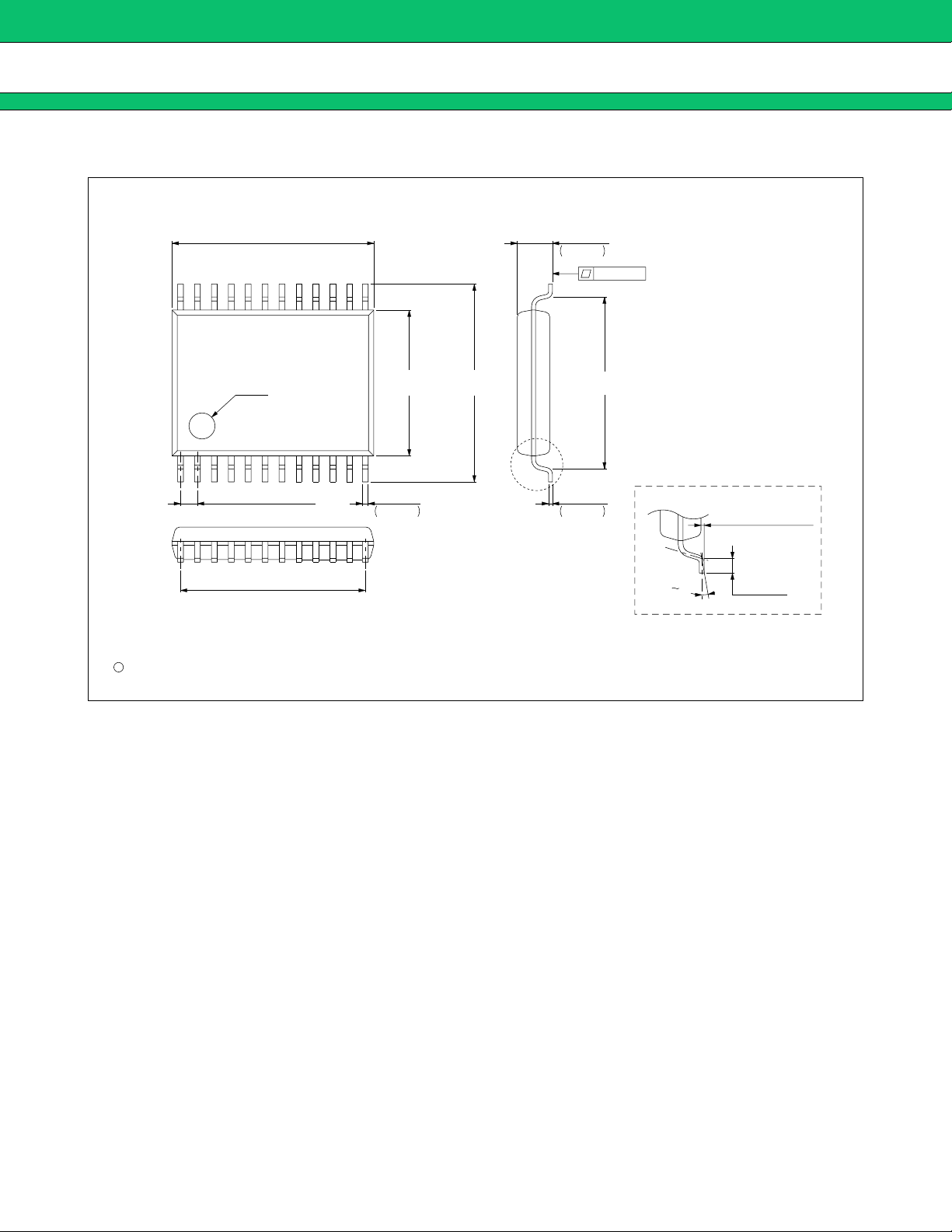
PACKAGE DIMENSION
0.20
■
MB3874/MB3876
24-pin plastic SSOP
(FPT-24P-M03)
*
7.75±0.10(.305±.004)
*
7.75±0.10(.305±.004)
INDEX
INDEX
0.65±0.12(.0256±.0047)
0.65±0.12(.0256±.0047)
7.15(.281)REF
7.15(.281)REF
*
*
(.220±.004) (.299±.008)
(.220±.004) (.299±.008)
+0.10
+0.10
–0.05
0.22
–0.05
0.22
+.004
+.004
.009
–.002
.009
–.002
7.60±0.20
7.60±0.20
* : These dimensions do not include resin protrusion.
+
+0.20
–0.10
"A"
"A"
1.25
1.25
.049
.049
0.15
0.15
.006
.006
(Mounting height)
–0.10
+.008
(Mounting height)
+.008
–.004
–.004
0.10(.004)
0.10(.004)
6.60(.260)5.60±0.10
6.60(.260)5.60±0.10
NOM
NOM
+0.05
+0.05
–0.02
–0.02
+.002
+.002
–.001
–.001
Details of "A" part
Details of "A" part
0 10°
0 10°
0.10±0.10(.004±.004)
0.10±0.10(.004±.004)
(STAND OFF)
(STAND OFF)
0.50±0.20
0.50±0.20
(.020±.008)
(.020±.008)
C
C
1994 FUJITSU LIMITED F24018S-2C-2
1994 FUJITSU LIMITED F24018S-2C-2
Dimensions in: mm (inches)
27
Page 28

MB3874/MB3876
FUJITSU LIMITED
For further information please contact:
Japan
FUJITSU LIMITED
Corporate Global Business Support Division
Electronic Devices
KAWASAKI PLANT, 4-1-1, Kamikodanaka
Nakahara-ku, Kawasaki-shi
Kanagawa 211-8588, Japan
Tel: 81(44) 754-3763
Fax: 81(44) 754-3329
http://www.fujitsu.co.jp/
North and South America
FUJITSU MICROELECTRONICS, INC.
Semiconductor Division
3545 North First Street
San Jose, CA 95134-1804, USA
Tel: (408) 922-9000
Fax: (408) 922-9179
Customer Response Center
Mon. - Fri.: 7 am - 5 pm (PST)
Tel: (800) 866-8608
Fax: (408) 922-9179
http://www.fujitsumicro.com/
Europe
FUJITSU MICROELECTRONICS EUR OPE GmbH
Am Siebenstein 6-10
D-63303 Dreieich-Buchschlag
Germany
Tel: (06103) 690-0
Fax: (06103) 690-122
http://www.fujitsu-fme.com/
Asia Pacific
FUJITSU MICROELECTRONICS ASIA PTE LTD
#05-08, 151 Lorong Chuan
New Tech Park
Singapore 556741
Tel: (65) 281-0770
Fax: (65) 281-0220
http://www.fmap.com.sg/
All Rights Reserved.
The contents of this document are subject to change without
notice. Customers are advised to consult with FUJITSU sales
representatives before ordering.
The information and circuit diagrams in this document are
presented as examples of semiconductor device applications,
and are not intended to be incorporated in devices for actual use.
Also, FUJITSU is unable to assume responsibility for
infringement of any patent rights or other rights of third parties
arising from the use of this information or circuit diagrams.
FUJITSU semiconductor devices are intended for use in
standard applications (computers, office automation and other
office equipment, industrial, communications, and
measurement equipment, personal or household devices, etc.).
CAUTION:
Customers considering the use of our products in special
applications where failure or abnormal operation may directly
affect human lives or cause physical injury or property damage,
or where extremely high levels of reliability are demanded
(such as aerospace systems, atomic energy controls, sea floor
repeaters, vehicle operating controls, medical devices for life
support, etc.) are requested to consult with FUJITSU sales
representatives before such use. The company will not be
responsible for damages arising from such use without prior
approval.
Any semiconductor devices have an inherent chance of
failure. You must protect against injury, damage or loss from
such failures by incorporating safety design measures into your
facility and equipment such as redundancy, fire protection, and
prevention of over-current levels and other abnormal operating
conditions.
If any products described in this document represent goods or
technologies subject to certain restrictions on export under the
Foreign Exchange and Foreign Trade Law of Japan, the prior
authorization by Japanese government will be required for
export of those products from Japan.
F0001
FUJITSU LIMITED Printed in Japan
 Loading...