

FUJIFILM FinePix F650 Service Manual
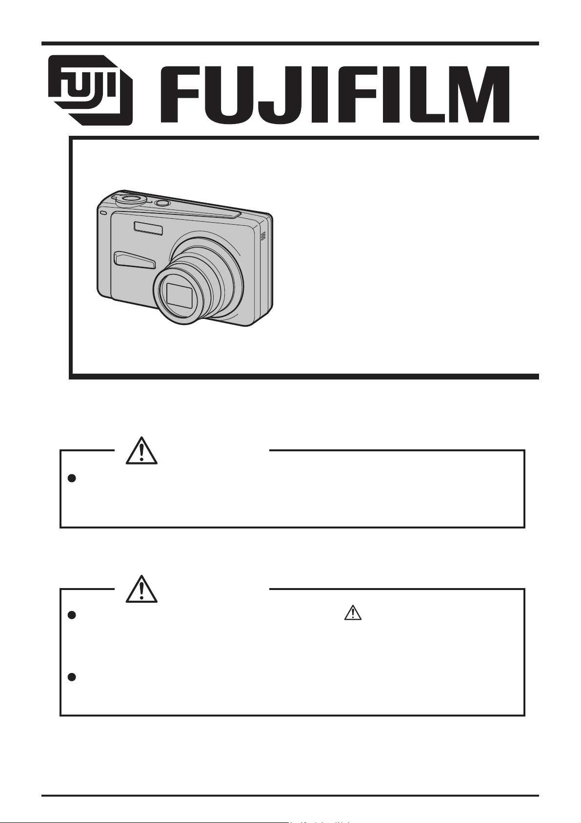
DIGITAL CAMERA
FinePix F650
SERVICE MANUAL
US/EU/EG/EE/AS/CH-Model
CAUTION
BECAUSE THIS PRODUCTIS RoHS LEAD-FREE COMPLIANT, USE THE DESIG-
NATED AFTER-SELES PARTS AND THE DESIGNATED LEAD-FREE SOLDER WHEN
PERFORMING REPAIRS. (Refer to page 3 to page 5)
WARNING
THE COMPONENTS IDENTIFIED WITH THE MARK “ ” ON THE SCHEMATIC
DIAGRAM AND IN THE PARTS LIST ARE CRITICAL FOR SAFETY.
PLEASE REPLACE ONLY WITH THE COMPONENTS SPECIFIED ON THE SCHEMATIC
DIAGRAM AND IN THE PARTS LIST.
IF YOU USE PARTS NOT SPECIFIED, IT MAY RESULT IN A FIRE AND AN
ELECTRICAL SHOCK.
FUJI PHOTO FILM CO., LTD.
Ref.No.:ZM00641-100
Printed in Japan 2006.06
FinePix F650 Service Manual
SAFETY CHECK-OUT
After correcting the original problem, perform the following
safety check before return the product to the customer.
1. Check the area of your repair for unsoldered or poorly
soldered connections. Check the entire board surface
for solder splasher and bridges.
2. Check the interboard wiring to ensure that no wires are
“pinched” or contact high-wattage resistors.
3. Look for unauthorized replacement parts, particularly
transistors, that were installed during a previous repair.
Point them out to the customer and recommend their
replacement.
4. Look for parts which, though functioning, show obvious
signs of deterioration. Point them out to the customer
and recommend their replacement.
5. Check the B + voltage to see it is at the values
specified.
6. Make leakage - current measurements to determine
that exposed parts are acceptably insulated from the
supply circuit before returning the product to the
customer.
7. CAUTION: FOR CONTINUED
PROTECTION AGAINST FIRE
HAZARD, REPLACE ONLY WITH
SAME TYPE 2.5 AMPERES 125V
FUSE.
2.5A 125V
2.5A 125V
8. WARNING:
RISK OF FIREREPLACE FUSE
AS MARKED
ATTENTION: AFIN D'ASSURER
UNE PROTECTION
PERMANENTE CONTRE LES
RISQUES D'INCENDIE,
REMPLACER UNIQUEMENT
PAR UN FUSIBLE DE MEME,
TYPE 2.5 AMPERES, 125 VOLTS.
TO REDUCE THE ELECTRIC
SHOCK, BE CAREFUL TO
TOUCH THE PARTS.
WARNING!
HIGH VOLTAGE
2

FinePix F650 Service Manual
RoHS lead-free compliance
Because this product is RoHS lead-free compliant, use the designated after-sales parts and the designated lead-free solder
when performing repairs.
<Background & Overview>
With the exception of parts and materials expressly excluded from the RoHS directive (*1), all the internal connections and
component parts and materials used in this product are lead-free compliant (*2) under the European RoHS directive.
*1: Excluded items (list of the main lead-related items)
• Lead included in glass used in fluorescent tubes, electronic components and cathode-ray tubes
• Lead in high-melting-point solder (i.e. tin-lead solder alloys that contain 85% lead or more)
• Lead in ceramic electronic parts (piezo-electronic devices)
• Mercury contained in fluorescent tubes is also excluded.
*2: Definition of lead-free
A lead content ratio of 0.1 wt% or less in the applicable locations (solder, terminals, electronic components, etc.)
<Reference>
RoHS: The name of a directive issued by the European Parliament aimed at restricting the use of
certain designated hazardous substances included in electrical and electronic equipment.
Designated substances (6): Lead, mercury, cadmium, hexavalent chromium, polybrominated biphenyls (PBBs) and
polybrominated diphenyl ether (PBDE)
<Lead-free soldering>
When carrying out repairs, use a designated lead-free solder, bearing in mind the differing work practices for conventional
solder (eutectic) and lead-free solder.
Differences in the soldering work for lead-free and eutectic solder
When the soldering work practices for eutectic solder and lead-free solder are compared, the main differences are as shown
below. In particular, when lead-free solder is used, the solder tends to be less workable than when eutectic solder is used.
Accordingly, the soldering techniques used must take that into account.
Difference
The solder starts melting later.
1
Poor wetting
2
Solder feed rate is difficult to control.
3
Wetting the insides of through holes is especially
4
difficult.
5
During repairs (or modifications) removing solder
from inside through holes is difficult.
6
There is serious carbonization of the soldering iron.
The surface is not glossy.
7
The initial melting point of lead-free solder is high, so you
have to get used to it.
Move the tip of the soldering iron around to heat the entire
connection to the melting temperature and assist wetting.
Use the solder (wire) diameter and soldering iron that are
best suited to connection being soldered.
First apply solder to the area immediately around the
through hold and then feed the solder into the hole.
Use a suitable wicking wire (with a suitable method and
heating) and a suction tool.
Either put solder onto the soldering iron tip after completing
the work, or turn the iron off frequently.
Learn to recognize the appearance of the surface.
Countermeasure
3
FinePix F650 Service Manual
Setting temperature during lead-free soldering
• Lead-free solder melting temperature
The melting point of eutectic (Sn-Pb) solder is 183°C, while the melting point of lead-free solder (Sn-Ag-Cu) is 30°C higher
at 220°C.
• Soldering iron tip temperature
The temperature setting for the soldering iron used should be such that the tip of the soldering iron is at the correct
bonding temperature for the connection. This temperature is normally set at around 100°C higher than the melting point of
the solder.
However, the actual temperature should take into account the shape and size of the soldering iron tip, the heat tolerance
of the connection and the workability of that temperature.
• Correct bonding temperature
The correct bonding temperature refers not to the temperature of the heat source, but to the bonding temperature that will
give the best bond strength.
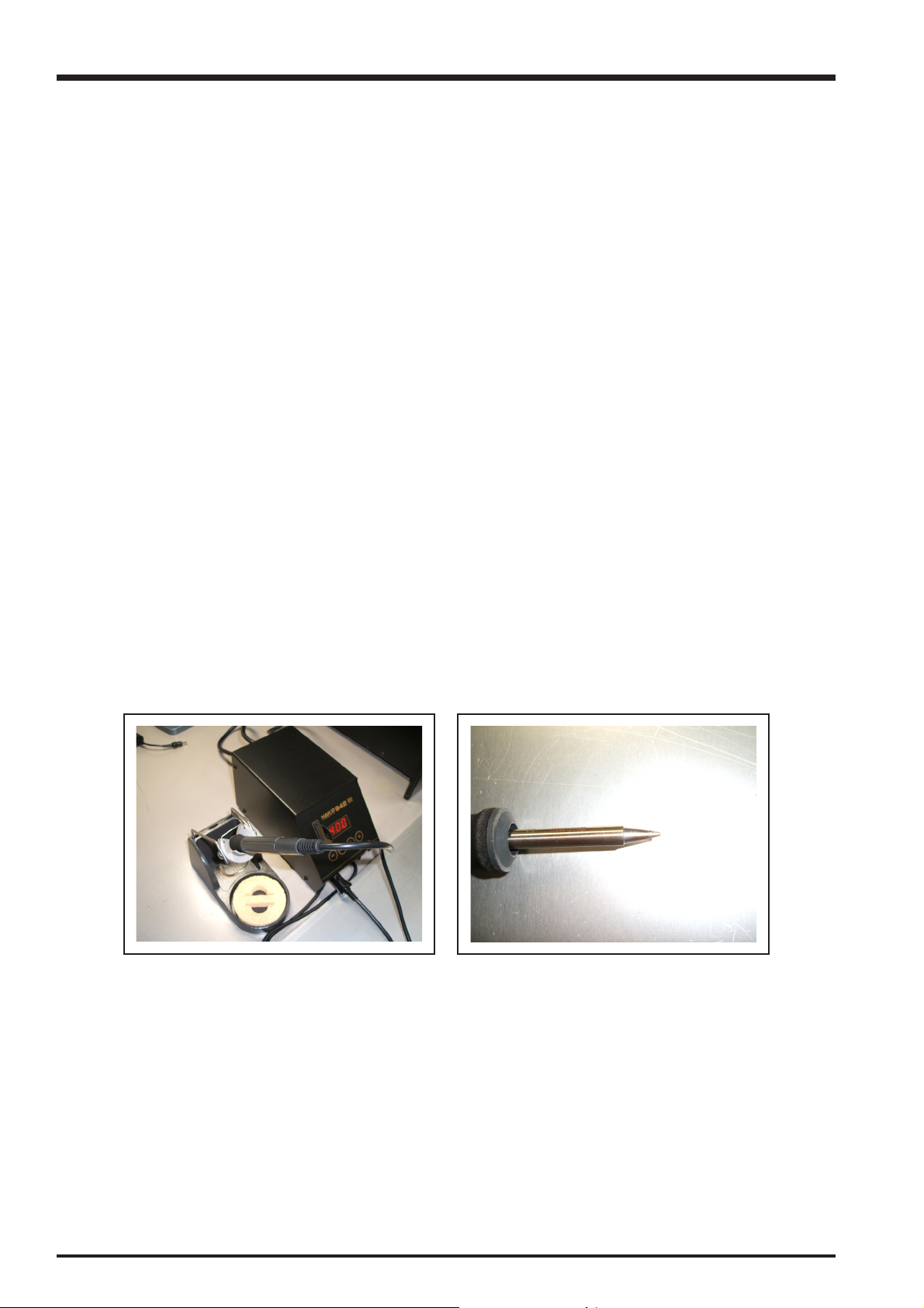
Precautions when soldering with lead-free solder
• Soldering iron maintenance
Because of the high soldering iron temperature in lead-free soldering, there is rapid carbonization of the flux adhering to
the tip of the soldering iron.
(1) Always cover the tip of the soldering iron with solder when it is not being used.
(2) If the tip is black from carbonization, wipe it gently with a paper towel soaked in alcohol until the solder will wet.
• Uniform heating of the board and components
To ensure that the lead-free solder wets the entire surface of the pattern and the lands despite its poor wetting
characteristics, you must move the tip of the soldering iron over a wide area to raise the temperature of the entire
connection.
Soldering iron
A soldering iron with a temperature control is best.
4
FinePix F650 Service Manual
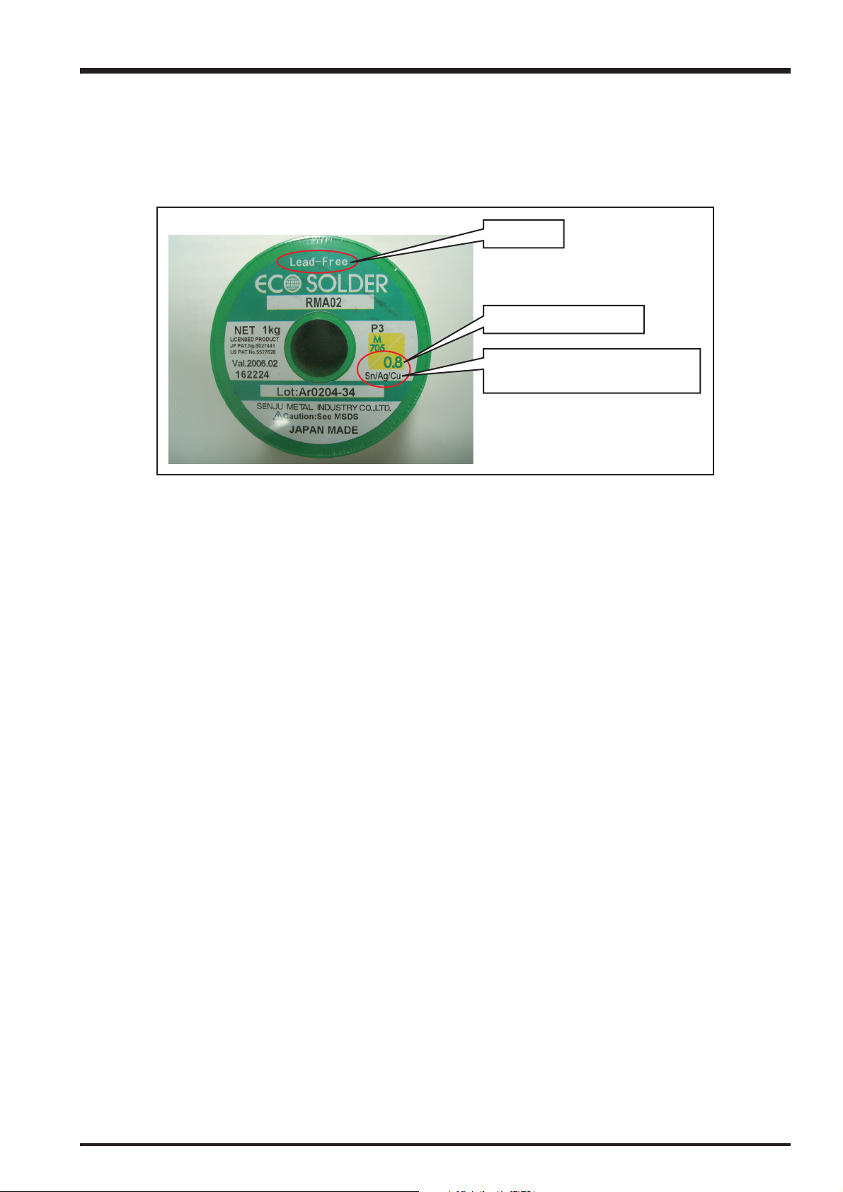
Solder wire (thread)
Use the lead-free solders specified below.
Solder type: Sn96.5Ag3Cu0.5 (Displayed symbol: SnAgCu)
Wire diameter: 0.6, 0.8 or 1.0 mm
Sample:
lead-free
Wire diameter 0.8mm
Solder type (Displayed symbol)
SnAgCu
Flux
Conventional flux can be used.
Solder application wires (mesh, wicking wire, etc.)
Conventional application wires can be used.
5

MEMO
FinePix F650 Service Manual
6

FinePix F650 Service Manual
CONTENTS
CONTENTS
1. General ........................................................... 8
1-1. Product specification .............................................. 8
1-2. Explanation of Terms ............................................ 11
1-3. Names of External Components .......................... 12
2. Disassembly ................................................. 13
2-1. Names of internal Components ............................13
2-2. Removing the CABI REAR ASSY ........................ 14
2-3. Disassembling the CABI REAR ASSY ................. 15
2-4. Removing the LCD monitor .................................. 16
2-5. Removing the LENS ASSY .................................. 17
2-6. Removing the MAIN PWB ASSY .......................... 18
2-7. Removing the BATTERY HOLDER ......................19
2-8. Removing the FLASH PWB ASSY .......................19
3. Schematics ................................................... 20
3-1. Description of CCD circuit operation .................... 20
3-1-1. Outline .................................................... 20
3-1-2. IC903 (CCD imager) ...............................20
3-1-3. IC901 (V driver) and IC905 (H driver) ..... 20
3-1-4. IC905 (CDS, AGC, A-D conversion) ....... 20
3-2. Description of CP1 circuit operation ..................... 21
3-2-1. Circuit Description ................................... 21
3-2-2. Outline of Operation ................................ 21
3-2-3. LCD Block ............................................... 21
3-2-4. Lens Drive Block ..................................... 22
3-3. Description of PWA power circuit operation ......... 22
3-3-1. Outline .................................................... 22
3-4. Description of ST1 flash circuit operation .............23
3-4-1. Charging circuit ....................................... 23
3-4-2. Flash Circuit ............................................ 24
3-5. Description of SYA circuit operation .....................25
3-5-1. Configuration and Functions ................... 25
3-5-2. Internal Communications Paths .............. 26
3-5-3. Key Operations ....................................... 26
3-5-4. Power Supply Control ............................. 27
3-6. Block Diagram ...................................................... 29
3-7. Overall connection Diagram ................................. 30
3-8. Circuit Diagrams ...................................................31
3-8-1. CCD BLOCK ........................................... 31
3-8-2. FLASH BLOCK .......................................32
3-8-3. MAIN BLOCK .......................................... 33
3-8-4. POWER BLOCK .....................................34
3-8-5. SYSTEM CONTROL BLOCK ................. 35
3-8-6. CA1 BLOCK ............................................ 36
3-8-7. CAA BLOCK ........................................... 37
3-8-8. DMA BLOCK ...........................................38
3-8-9. PWA BLOCK ........................................... 39
3-8-10. SYA BLOCK ............................................40
3-8-11. TCA BLOCK ............................................ 41
3-8-12. STA BLOCK ............................................ 42
3-8-13. LENS BLOCK ......................................... 43
3-9. Mounted Parts Diagrams ...................................... 44
3-9-1. ST1/ST2 PWB ASSY .............................. 44
3-9-2. CA1 PWB ASSY .....................................45
3-9-3. CP1 PWB ASSY .....................................47
4. Adjustments .................................................. 49
4-1. Important point before Adjustment ....................... 49
4-1-1. The handling of image files in internal
memory ................................................... 49
4-1-2. Adjustment when Replacing
Major Parts ............................................. 50
4-2. Measuring Instruments Used ............................... 50
4-3. Use Jig list ............................................................ 50
4-4. Calibration method of pattern box ........................ 51
4-5. Adjustment software installation ........................... 51
4-5-1. Various downloading software
decompressions, preservation methods,
and notes ................................................51
4-6. Connecting to the PC for Adjustment ................... 52
4-7. Adjustment Software Description ......................... 53
4-8. MAIN PWB ASSY initialization ............................. 54
4-9. LENS Adjustment ................................................. 58
4-10. AWB Adjustment .................................................. 60
4-11. CCD Defect Detection .......................................... 62
4-12. CCD Black Defect Detection ................................ 64
4-13. Updating the Firmware .........................................66
4-14. Completion Settings ............................................. 69
5. Inspection ..................................................... 71
5-1. Required Measuring Equipment ...........................71
5-2. Connection of Measuring Equipment ................... 71
5-3. Inspection and Factory Settings ........................... 72
6. Parts List....................................................... 76
6-1. Packing and Accessories ..................................... 76
6-1-1. US-model ................................................ 76
6-1-2. US-model (JP Production) ...................... 77
6-1-3. EU-model ................................................ 78
6-1-4. EG-model ................................................ 79
6-1-5. EE-model ................................................80
6-1-6. AS-model ................................................81
6-1-7. CH-model ................................................ 82
6-2. Mechanical Block ................................................. 83
6-2-1. US/AS/CH-model .................................... 83
6-2-2. US-model (JP Production) ...................... 84
6-2-3. EU/EG/EE-model .................................... 85
6-3. Electrical parts ......................................................87
7. Appendix....................................................... 88
7-1. List of Related Technical Updates Issued ............ 88
7
1. General
FinePix F650 Service Manual
1. General
1-1. Product specification
System
Model Digital camera FinePix F650
Effective pixels 6.0 million pixels
CCD 1/2.5-inch square pixel CCD
Storage media Internal memory (approx. 26 MB)/xD-Picture Card (16/32/64/128/256/512 MB/1 GB)
File format Still image: DCF-compliant
Compressed: Exif ver.2.2 JPEG, DPOF-compatible
*Design rule for Camera File System compliant DPOF compatible
Movie: AVI format, Motion JPEG
Audio: WAVE format, Monaural sound
Number of recorded pixels Still image: 2816
640 × 480 pixels ( / / / / )
Lens Fujinon 5
F2.8-F4.7
Focal length f=5.8 mm-29 mm
(Equivalent to approx. 35 mm-175 mm on a 35 mm camera)
Digital zoom Approx. 4.4
Aperture (Wide-angle) F2.8 to F8 (Up to 10 steps)
Focal range Normal: approx. 60 cm (2.0 ft.) to infinity
Macro: approx. 12 cm (4.7 in.) to 80 cm (2.6 ft.)
Super Macro: approx. 3 cm (1.2 in.) to 20 cm (7.9 in.)
Sensitivity AUTO/Equivalent to ISO 64/100/200/400
Photometry TTL 256-zones metering
Exposure control Program AE/Aperture priority AE/Shutter priority AE
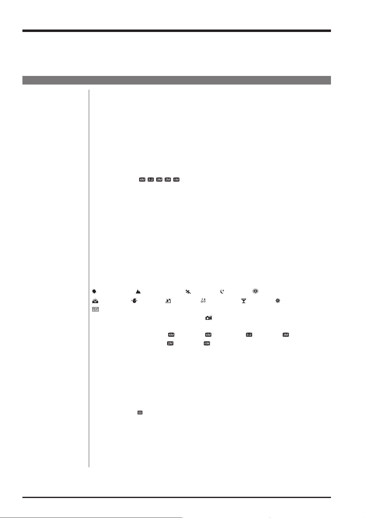
Scene position
Exposure compensation -2 EV to +2 EV in 1/3 EV-step increments ( , A, S)
Shutter speed 2 sec. to 1/2000 sec. (depend on Exposure mode)
Continuous shooting Number of recorded frames:
Focus Mode: Single-AF
White balance Automatic scene recognition/Preset (Fine, Shade, Fluorescent (Daylight),
Self-timer Approx. 2 sec./10 sec.
Flash type Auto flash
Flash mode Auto, Red-eye Reduction, Forced Flash, Suppressed Flash, Slow Synchro,
LCD monitor 3.0 inches, Aspect ratio: 4:3; 230,000 pixels low-temperature polysilicon TFT, Approx.
(PORTRAIT), (LANDSCAPE), (SPORT), (NIGHT), (FIREWORKS),
AF system: TTL contrast-type
AF frame selection: AF (CENTER)
Fluorescent(Warm White), Fluorescent (Cool White), Incandescent)
Effective range: (
Red-eye Reduction + Slow Synchro
100% coverage
×
optical zoom lens
(SUNSET), (SNOW), (BEACH), (MUSEUM), (PARTY), (FLOWER),
(TEXT)
×
2112 pixels/2816 × 1880 pixels/2048 × 1536 pixels/1600 × 1200 pixels/
×
(5× optical zoom lens is used together: Max. zoom scale: approx. 22×)
F 6 frames/ N 12 frames/ 13 frames/ 22 frames/
29 frames/ 140 frames (Max. 1.7 frames/sec.)
: AUTO):Wide-angle: approx. 60 cm-4.6 m (2.0 ft.-15.1 ft.)
Telephoto: approx. 60 cm-2.7 m (2.0 ft.-8.9 ft.)
Macro: approx. 30 cm-80 cm (1.0 ft.-2.6 ft.)
8

FinePix F650 Service Manual
1. General
System
Movie 640 × 480 pixels/320 × 240 pixels ( / )
(30 frames per second with monaural sound)
A series of continuous image can be recorded depending on the available space on an
xD-Picture Card or internal memory. Zoom cannot be used during movie recording.
Photography functions Best framing, Frame No. memory
Playback functions Trimming, Automatic playback, Multi-frame playback, Sorting by date, Image rotate,
Voice memo
Other functions PictBridge, Exif print, Language (English, Francais, Deutsch,
Time difference, FinePix photo mode (
-mode)
, Italiano, , ),
Input/Output Terminal
A/V OUT NTSC/PAL-type (with monaural sound)
(Audio/Visual output)
Digital input/output USB 2.0
DC input socket AC Power Adapter AC-5VX (sold separately)
Power Supply and Others
Power supply Use one of the following
• Rechargeable Battery NP-40N (included)/NP-40 (sold separately)
• AC Power Adapter AC-5VX (sold separately)
Guide to the number of
available frames for
battery operation
According to the CIPA (Camera & Imaging Products Association) standard procedure for
measuring digital still camera battery consumption (extract):
When using a battery, use the battery supplied with the camera. The storage media should
be xD-Picture Card.
Pictures should be taken at a temperature of +23°C (+73°F), with the LCD monitor turned
on, the optical zoom moved from full wide-angle to full telephoto (or vice-versa) and back
again to its original position every 30 seconds, the flash used at full power every second
shot and the camera turned off and then on again once every 10 shots.
• Note: Because the number of available shots varies depending on the level of charge in
the battery, the figures shown here for the number of available shots using the
battery is not guaranteed.
The number of available shots will also decline at low temperatures.
Camera dimensions 104.7 mm
(W/H/D) (not including accessories and attachments)
Camera mass (weight) Approx. 170 g/6.0 oz. (not including accessories, battery and xD-Picture Card)
Weight for photography Approx. 190 g/6.7 oz. (including battery and xD-Picture Card)
Operating conditions Temperature: 0
80% humidity or less (no condensation)
Battery Type Number of frames
NP-40N Approx. 150 frames
×
60.6 mm × 30.8 mm/4.1 in. × 2.4 in. × 1.2 in.
o
C to +40oC (+32oF to +104oF)
9
1. General
FinePix F650 Service Manual
Power Supply and Others
Accessories included z Rechargeable Battery NP-40N (1) Soft case included
z Strap (1)
z Battery Charger BC-40 (1)
z A/V cable for FinePix F650 (1) Including plug to pin-plug
z USB cable for FinePix F650 (1)
z CD-ROM (1) Software for FinePix CX
z Owner’s Manual (1)
Optional accessories z xD-Picture Card
16MB/32MB/64MB/128MB/256MB/512MB/1GB
z Battery Charger BC-65S
z Rechargeable Battery NP-40 (750 mAh)
z AC Power Adapter AC-5VX
z Soft Case SC-FXA03
z Image Memory Card Reader DPC-R1
• Compatible with xD-Picture Card of 16 MB to 512 MB, and SmartMedia of 3.3 V,
4 MB to 128 MB.
z PC Card Adapter DPC-AD
• Compatible with xD-Picture Card of 16 MB to 512 MB, and SmartMedia of 3.3 V,
2 MB to 128 MB.
z CompactFlash Card Adapter DPC-CF
×
2
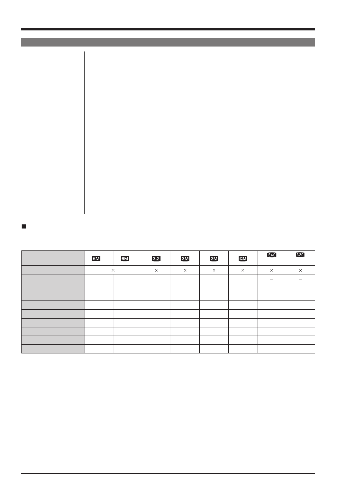
Standard number of available frames/recording time per xD-Picture Card and internal memory
The number of available
that the divergence between standard number of
xD-Picture Cards with higher capacities.
Quality setting
Number of recorded pixels
Image data size
Internal memory (approx. 26 MB)
16 MB
32 MB
64 MB
128 MB
256 MB
512 MB
1 GB
, recording time or file size varies slightly depending on the subjects photographed. Note also
frames
frames
F
2816
2.9 MB
9
5
10
21
43
87
174
2112
1.4 MB
19
10
21
43
86
173
347
N
2816 1880 2048 1536 1600 1200
1.3 MB
21 35 45 219
12
24
48
97
195
389
349 695 780 1305 1640 7996
and the actual number of
640 480 640 480 320 240
780 KB
20
40
81
163
326
652
630 KB
25
51
102
204
410
819
130 KB
1999
3995
124
249
499
999
frames
(30 fps) (30 fps)
30 sec. 48 sec.
17 sec.
34 sec.
70 sec.
140 sec.
280 sec.
9.3 min.
18.7 min. 29.6 min.
is greater for
27 sec.
55 sec.
110 sec.
221 sec.
7.4 min.
14.7 min.
10

FinePix F650 Service Manual
1. General
1-2. Explanation of Terms
EV: A number denotes Exposure Value. The EV is determined by the brightness of the subject
and sensitivity (speed) of the film or CCD. The number is larger for bright subjects and
smaller for dark subjects. As the brightness of the subject changes, a digital camera
maintains the amount of light hitting the CCD at a constant level by adjusting the aperture
and shutter speed.
When the amount of light striking the CCD doubles, the EV increases by 1. Likewise, when
the light is halved, the EV decreases by 1.
Frame rate (fps): The frame rate refers to the number of images (frames) that are photographed or played
back per second. For example, when 10 frames are continuously photographed in a 1-
second interval, the frame rate is expressed as 10 fps.
For reference, TV images are displayed at 30 fps (NTSC).
JPEG: Joint Photographic Experts Group
A file format used for compressing and saving color images. The higher the compression
rate, the greater the loss of quality in the decompressed (restored) image.
Motion JPEG: A type of AVI (Audio Video Interleave) file format that handles images and sound as a
single file. Images in the file are recorded in JPEG format. Motion JPEG can be played
back by QuickTime 3.0 or later.
Smear: A phenomenon specific to CCDs whereby white streaks appear on the image when there
is a very strong light source, such as the sun or reflected sunlight, in the photography
screen.
WAVE A standard format used on Windows systems for saving audio data. WAVE files have the
“.WAV” file extension and the data can be saved in either compressed or uncompressed
format. Uncompressed recording is used on this camera.
WAVE files can be played back on a personal computer using the following software:
Windows: MediaPlayer
Macintosh: QuickTime Player
* QuickTime 3.0 or later
White Balance: Whatever the kind of the light, the human eye adapts to it so that a white object still looks
white. On the other hand, devices such as digital cameras see a white subject as white by
first adjusting the color balance to suit the color of the ambient light around the subject.
This adjustment is called matching the white balance.
Exif Print: Exif Print Format is a newly revised digital camera file format that contains a variety of
shooting information for optimal printing.
11

1. General
1-3. Names of External Components
FinePix F650 Service Manual
Shutter button
Mode dial
Self-timer lamp
Flash
Lens (lens cover)
Microphone
Indicator lamp
MENU/OK button
4-direction ( ) button
POWER button
Speaker
W (Wide zoom) button
T (Tele zoom) button
LCD monitor
Tripod mount
Battery cover
DISP (Display)/
BACK button
xD-Picture Card slot
Battery compartment
Battery release catch
W
T
(Playback) button
Photo mode ( ) button
M
E
NU
/O
K
D
ISP/
BACK
Terminal cover
DC IN 5V socket
A/V OUT
(Audio/Visual output)
socket
USB socket
Strap mount
12
FinePix F650 Service Manual
2. Disassembly
2-1. Names of internal Components
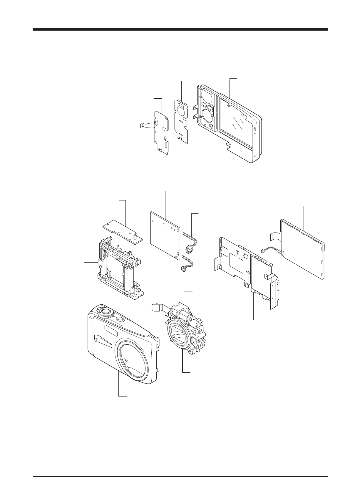
2. Disassembly
OPERATION BUTTON
FLASH PWB ASSY
CABI R ASSY
KEY UNIT
MAIN PWB ASSY
LCD
SPEAKER
BATTERY
HOLDER ASSY
MICROPHONE
MONITOR HOLDER
LENS ASSY
CABI F ASSY
13

2. Disassembly
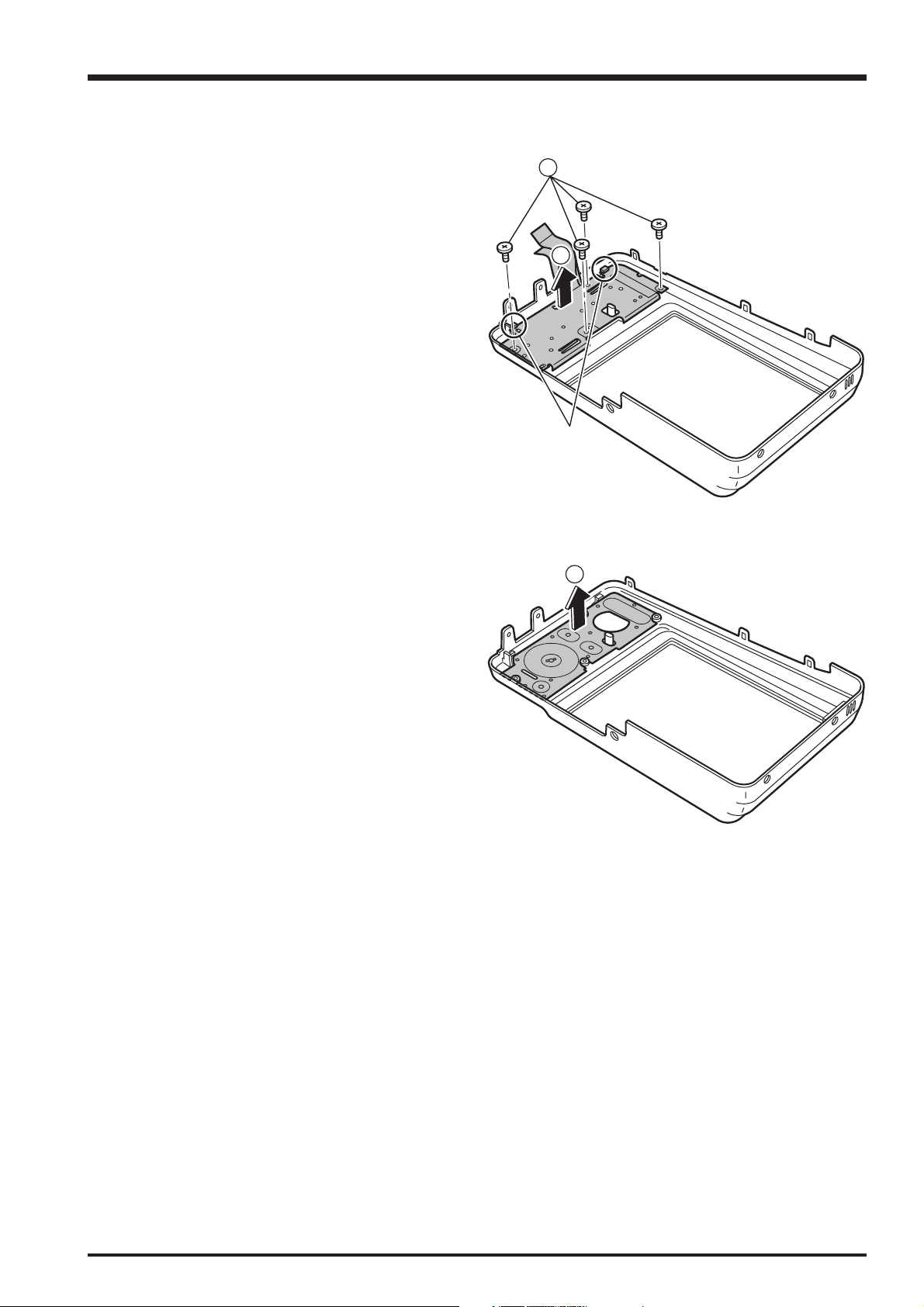
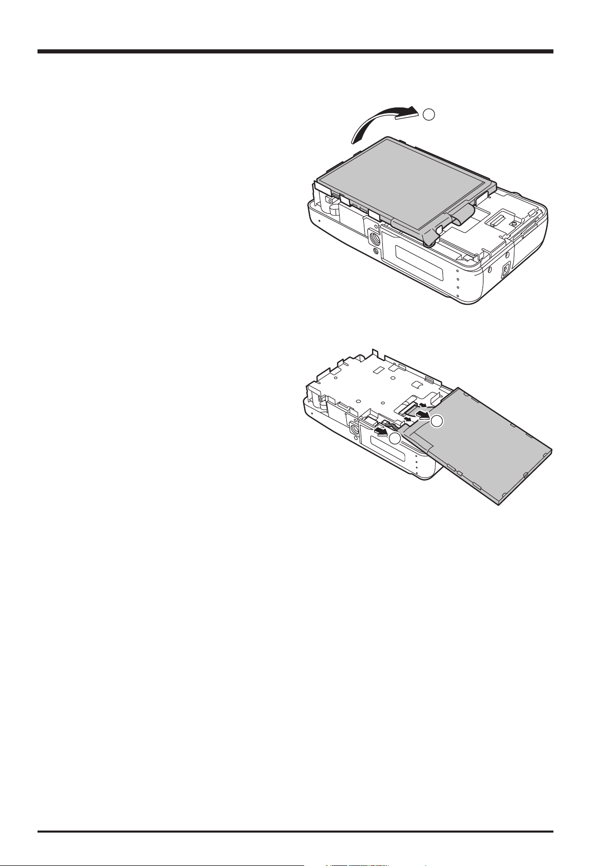
2-2. Removing the CABI REAR ASSY
FinePix F650 Service Manual
(1) Remove the 2 special screws (M1.7 x 4.0).
(2) Remove the 2 screws (M1.7 x 3.0).
(3) Remove the 2 screws (M1.7 x 2.5).
(4) Set the mode dial to the "SP" position and disengage
the 3 hooks as you remove the CABI REAR ASSY in
the direction of the arrow. (Set the mode dial to "SP" for
re-assembly also.)
3
1
2
HOOK
SP
(5) Unlock the connector and remove the KEY UNIT FPC.
[Assembly]
Assemble by performing the removing procedure in
reverse.
4
5
14
FinePix F650 Service Manual
HOOK
1
2
3
2-3. Disassembling the CABI REAR ASSY
(1) Remove the 4 screws (M1.4 x 2.0).
(2) Disengage the 2 hooks as you remove the KEY UNIT.
2. Disassembly
(3) Remove the OPERATION BUTTON.
[Assembly]
Assemble by performing the disassembly procedure in
reverse.
15
2. Disassembly
2-4. Removing the LCD monitor
FinePix F650 Service Manual
(1) Remove the LCD monitor in the direction of the arrow.
(2) Remove the connector and then remove the LCD FPC.
(3) Remove the LCD wire harness.
[Assembly]
Assemble by performing the removing procedure in
reverse.
1
2
3
16
FinePix F650 Service Manual
2-5. Removing the LENS ASSY
2. Disassembly
(1) Remove the 3 screws (M1.7 x 4.0).
(2) Remove the MONITOR HOLDER.
(3) Remove the LENS connector.
(4) Remove the connector and then remove the CCD FPC.
(5) Remove the LENS ASSY in the direction of the arrow.
1
2
5
3
[Assembly]
Assemble by performing the removing procedure in
reverse.
4
17

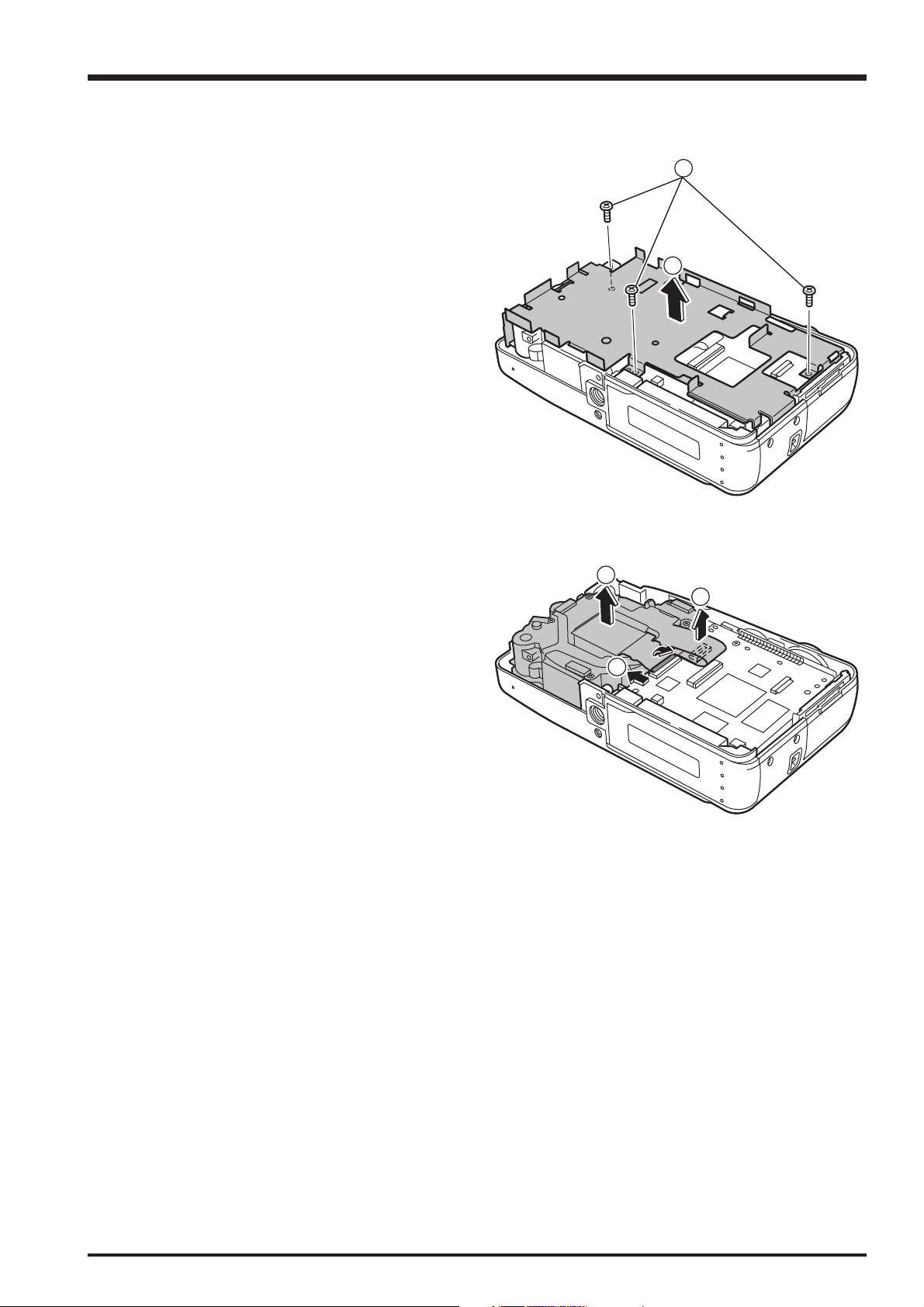
2. Disassembly
2-6. Removing the MAIN PWB ASSY
FinePix F650 Service Manual
(1) Remove the solder at 5 points.
(2) Remove the screw (M1.7 x 4.0).
(3) Open the BATTERY COVER.
(4) Remove the MAIN PWB ASSY in the direction of the
arrow.
[Notes on Assembly]
(1) Run the MIC wire harness as shown in the figure on the
right.
2
4
1
3
1
1
(2) Install the MAIN PWB ASSY with the BATTERY
COVER open, (to prevent damage to the BATTERY
COVER detector switch).
[Assembly]
Assemble by performing the removing procedure in
reverse.
18
FinePix F650 Service Manual
1
2
3
2-7. Removing the BATTERY HOLDER
(1) Remove the 2 screws (M1.7 x 4.0).
(2) Raise the BATTERY HOLDER in the direction of the
arrow.
(3) Open the right side of the CABI at the strap mount
outwards slightly and remove the BATTERY HOLDER.
[Assembly]
Assemble by performing the removing procedure in
reverse.
2. Disassembly
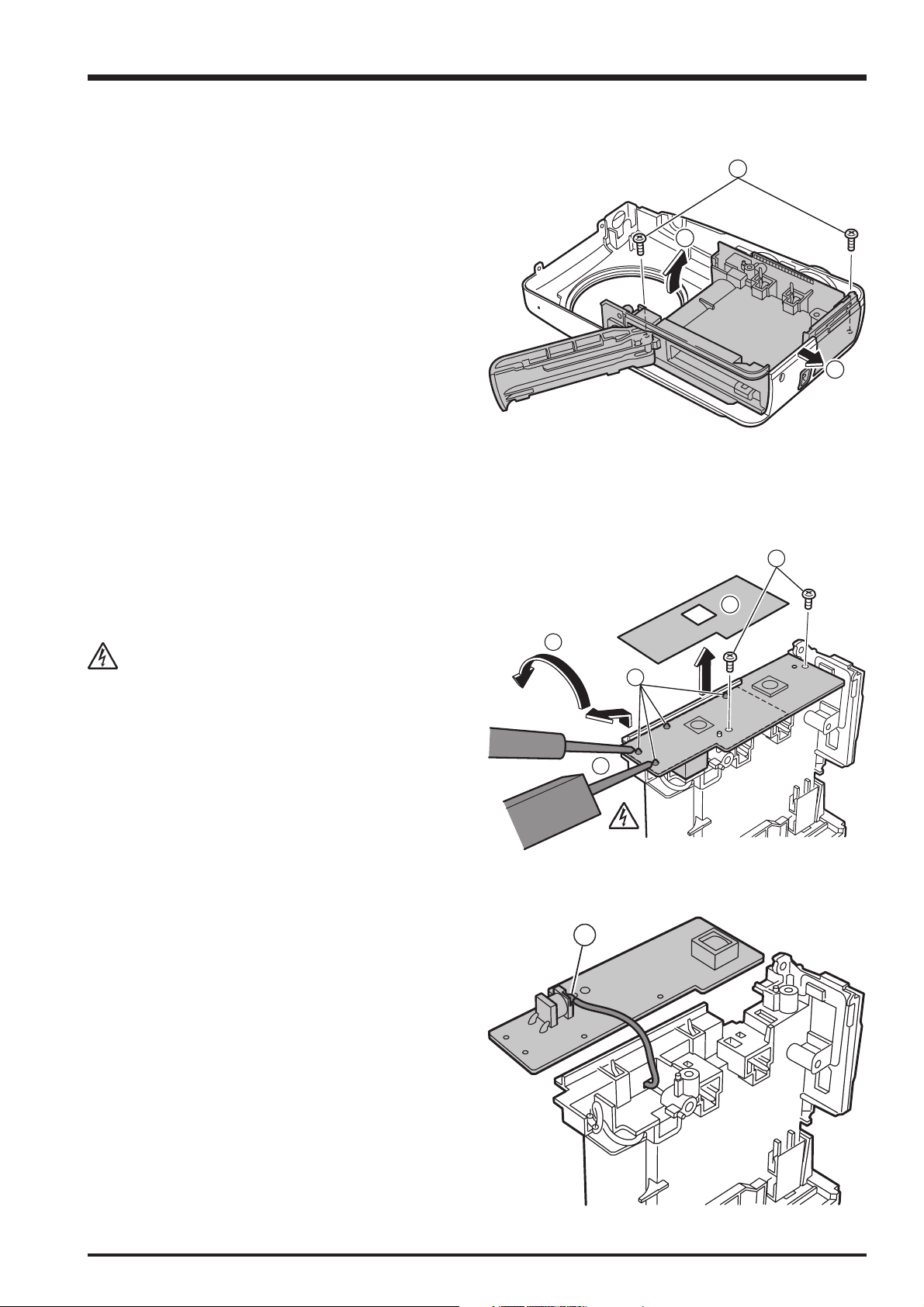
2-8. Removing the FLASH PWB ASSY
(1) Peel off the FLASH PWB SPACER.
(2) Discharge the current across the (+) RD and (-) BK
terminals.
Take care not to touch the FLASH PWB ASSY before
discharging.
(3) Remove the solder at 4 points.
(4) Remove the 2 screws (M1.7 x 4.0).
(5) Remove the FLASH PWB ASSY in the direction of the
arrow.
(6) Remove the trigger coil solder.
4
1
5
3
2
6
[Assembly]
Assemble by performing the removing procedure in
reverse.
19
3. Schematics
FinePix F650 Service Manual
3. Schematics
3-1. Description of CCD circuit
Ø7B
Ø8
V
V
14
13
12
Ø7A
V
ØHLD
Ø6
V
V
10
11
Ø4
Ø5A
Ø5B
V
V
V
7
8
9
Ø3A
Ø3B
ØST
V
V
V
6
4
5
Ø1A
Ø1B
Ø2
V
V
V
1
3
2
operation
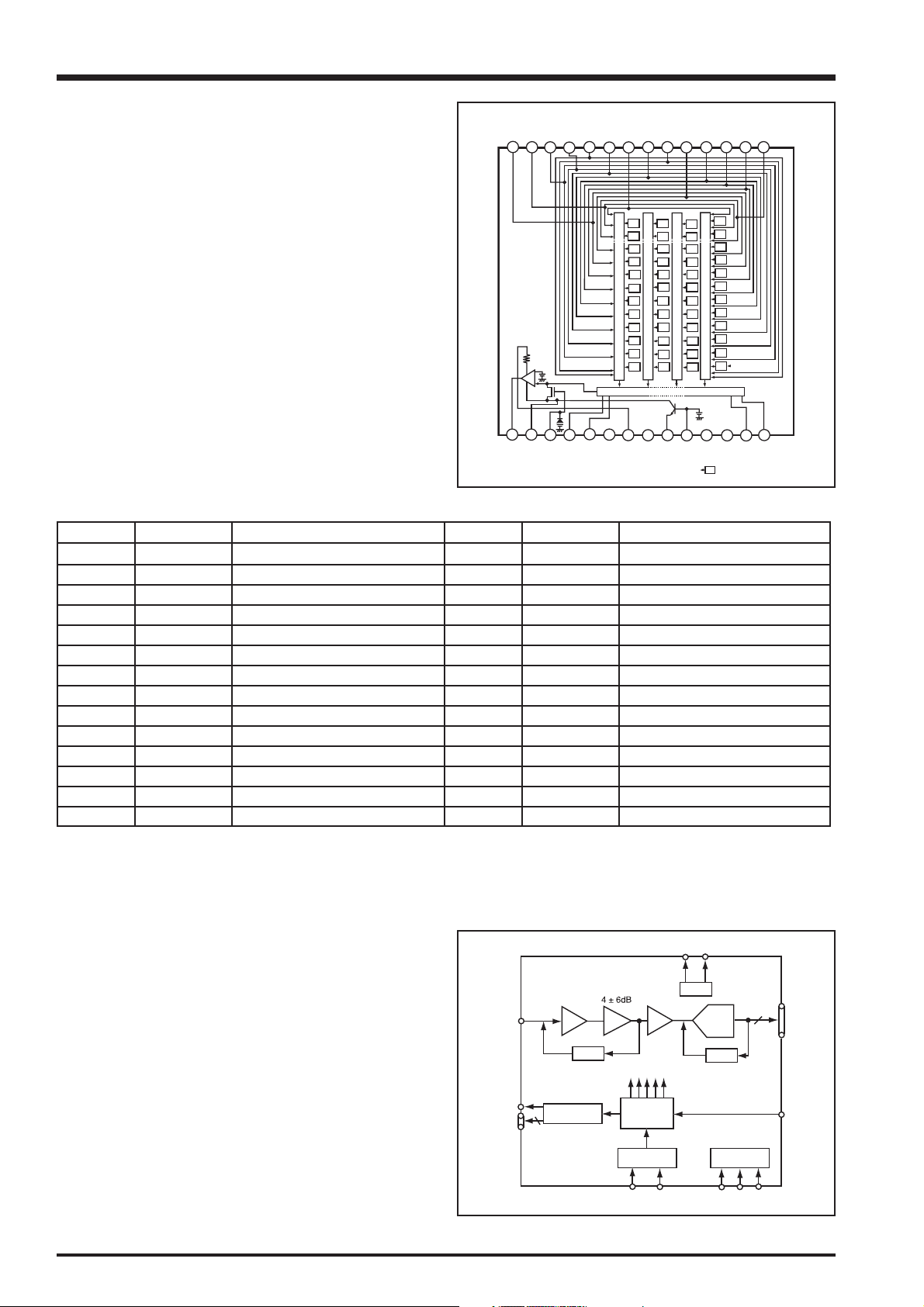
3-1-1. Outline
The CCD peripheral circuit block is primarily composed of
the following ICs:
IC903 (ICX624FQN) CCD imager
IC905 (AD9949AKCPZ) H driver, CDS, AGC, A-D conversion
IC901 (CXD3443GA), V drivers
3-1-2. IC903 (CCD imager)
• Interline-type CCD image sensor
• Image size: 7.18 mm diagonal (1/2.5-inch)
G
R
G
R
G
R
G
R
Vertical register
G
R
G
R
Horizontal register
B
G
B
G
B
G
B
G
B
G
B
G
• Total pixels: 2892 (H) x 2138 (V)
• Recorded pixels: 2816 (H) x 2112 (V)
16
15
DD
OUT
V
V
19
20
18
17
RG
Ø1B
Ø
H
Ø2B
H
GND
21
23
22
SUB
GND
GND
Ø
<Fig 3-1. CCD block diagram>
Terminal no. Terminal symbol Terminal description Terminal no. Terminal symbol Terminal description
1VØ1AVertical register transfer clock
2VØ1BVertical register transfer clock
3VØ2Vertical register transfer clock
4VØ3AVertical register transfer clock
5VØ3BVertical register transfer clock
6VØSTHorizontal addition control clock
7VØ4Vertical register transfer clock
8VØ5AVertical register transfer clock
9VØ5BVertical register transfer clock
10 VØ
11 VØ
12 VØ
13 VØ
14 VØ
HLD
7A
7B
Horizontal addition control clock
6
Vertical register transfer clock
Vertical register transfer clock
Vertical register transfer clock
8
Vertical register transfer clock
15 V
16 V
17 ØRG Reset gate clock
18 HØ
19 HØ
20 GND GND
21 GND GND
22 GND GND
23 ØSUB Board clock
24 C
25 NC –
26 V
27 HØ
28 HØ
out
DD
SUB
Signal output
Circuit power supply
1B
Horizontal register transfer clock
2
Horizontal register transfer clock
Board bias
L
1A
2A
Protective transistor bias
Horizontal register transfer clock
Horizontal register transfer clock
<Table 3-1. Explanation of the CCD terminals>
B
G
G
R
B
G
G
R
B
G
G
R
B
G
G
R
B
G
G
R
B
G
(Note)
G
R
25
26
24
SUB
C
(Note): Photosensor
NC
27
L
V
Ø1A
H
28
Ø2A
H
3-1-3. IC901 (V driver) and IC905 (H driver)
The H driver and V driver are necessary to generate the
clocks that drive the CCD (vertical register transfer clock,
horizontal register transfer clock and electronic shutter
clock). IC 901 comprise the V driver, XV1-XV6 output from
IC101 comprises the vertical register transfer clock, and XSG
is superposed in IC901 to generate a 3-value pulse. The
XSUB output by IC101 serves as the clearing pulse for the
electronic shutter. The H driver is built into IC905 and the
clocks for H1, H2 and RG are created by IC905.
3-1-4. IC905 (CDS, AGC, A-D conversion)
Video signals output from the CCD are input via pin 27 on
IC905. Inside the IC are a sampling hold block, AGC block
and A-D conversion block. The sampling phase and AGC
amplifier settings are specified using serial data to pin 32.
The video signals are A-D converted and output as 12-bit
data.
20
CCDIN
RG
H1-H4
VRB
VRT
VREF
2~36 dB
VGA
PxGA
CDS
HORIZONTAL
4
DRIVERS
CLAMP
INTERNAL
CLOCKS
PRECISION
TIMING
CORE
SYNC
GENERATOR
VD
HD
<Fig 3-2. IC905 block diagram>
ADC
CLAMP
INTERNAL
REGISTERS
SL
SCK
12
SD ATA
DOUT
CLI

FinePix F650 Service Manual
3. Schematics
3-2. Description of CP1 circuit
operation
3-2-1. Circuit Description
Digital clamp
The black levels for the CCD output data are evened up
across the line by subtracting the averaged value for the
optical black sections of the CCD from the subsequent data.
The average value for the optical black sections of the CCD
is obtained by multiplying the value for the previous line by a
coefficient k and multiplying the value for the current line by a
coefficient k-1 and then taking the sum of the multiples.
Signal processor
γγ
γ (gamma) correction circuit: γ (gamma) correction is
γγ
performed to ensure that there is a linear relationship
between the optical input to the camera and the optical
output of the screen receiving the image.
Color signal generation circuit: This circuit converts the
CCD data to R, G and B signals.
Matrix circuit: This circuit uses the R, G and B signals to
generate Y, R-G and B-G signals.
Horizontal/vertical aperture circuit: This circuit generates
the aperture signal.
3-2-2. Outline of Operation
When the shutter is released, the microprocessor sends a
reset signal and a serial signal (TAKE A PICTURE
instruction) to the ASIC and CPU and operation begins.
When the TG/SG drives the CCD, the image data passes
through A-D conversion and CDS and is sent to the ASIC as
12-bit data. The received (input) data is then input to SDRAM
via the digital clamp.
This data is used to calculate the AF, AE, AWB, shutter and
AGC values, and then 3 exposures are normally taken to
obtain the best possible image. The data for the images
stored in SDRAM is loaded into the CPU and the colors are
generated. Each pixel in the R, G and B data is interpolated
from the surrounding data to generate the R, G and B pixel
data. After AWB and γ (gamma) correction, a matrix is
generated and aperture compensation is applied for the Y
signal. The resulting data is then subjected to JPEG
compression and recorded onto card memory (xD-Picture
card). When the data is output to an external device, the data
is fetched from memory and output serially via USART. When
the image is played back on an LCD or monitor, the data is
transferred from memory to SDRAM, expanded into the
SDRAM display area and then displayed.
AE/AWB/AF calculation circuit
This circuit calculates the AE and AWB values by dividing the
screen into 64 zones and calculates the AF value by dividing
the screen into 6 zones.
SDRAM controller circuit
This circuit outputs the address, RAS, CAS and AS used for
SDRAM control. This circuit also refreshes the SDRAM.
Communication control
SIO: This is the interface with the 8-bit microprocessor.
SIO for LCD, PWM and PIO: This makes it possible to
switch between PWM output and individual I/O in 8-bit
parallel I/O.
TG/SG
This controls and generates timing for the 6-megapixel CCD.
Digital encoder
This generates chroma signals from the color difference
signals.
3-2-3. LCD Block
The LCD display circuit is located on the CP1 PWB and
consists of the LCD driver IC (IC171) and its peripheral
circuits.
Signals from the ASIC, consisting of 8-bit digital signals,
serial control signals and synchronization control signals, are
input to the LCD driver IC.
These signals are then converted to RGB signals by the LCD
driver IC. The serial control signals are used to control
factors such as brightness and image quality.
The larger the potential differences between the COM
signals (common electrode voltage: AC fixed) and the R, G
and B signals, the greater the LCD pixel closure and the
darker the display. Conversely, the smaller the potential
difference, the less the LCD pixel closure and the brighter the
display.
21

3. Schematics
FinePix F650 Service Manual
3-2-4. Lens Drive Block
Focus drive
The 8-bit serial data signals (L_DATA along with L_STB,
FCLK, L_ST and L_SCLK) output from the ASIC (IC 101) are
driven by the motor driver (IC951) and in turn drive the
stepping motor used for focusing (AF_M0, AF_M1, AF_M2
and AF_M3).
The focus reference position is detected by a photointerrupter (AF_HOME) in the lens block.
Zoom drive
The signals (ZIN1 and ZIN2) output from the ASIC (IC101)
are subjected to a constant-current drive (ZM(+) and ZM(-))
from the motor driver (IC 951) and in turn drive the DC motor
for the zoom.
The zoom reference position is detected by a photo-reflector
(ZM_HOME) in the lens block. To ascertain the zoom
position, the ASIC (IC101) counts the output from a photointerrupter (ZM_ENC) in the lens block.
Shutter drive
The shutter drive signals (SIN1 and SIN2) output from the
ASIC (IC101) are subjected to a constant-current drive (SD1
and SD2) from the motor driver (IC 951) and in turn open
and close the mechanical shutter.
Aperture drive
The 8-bit serial data signals (L_DATA along with L_STB,
ICLK, L_ST and L_SCLK) output from the ASIC (IC 101) are
driven by the motor driver (IC951) and in turn widen or
narrow the aperture (ST1, ST2, ST3 and ST4).
3-3. Description of PWA power
circuit operation
3-3-1. Outline
The power circuit consists primarily of the following blocks:
• Switching power controller (IC501)
• Analog 12V (A) power output (L5003, Q5001)
• Analog -7.5V (A) power output (L5005, Q5005, IC502)
• Digital VDD 3V power output (L5001)
• Digital VDD 1.2V power output (L5002)
• Backlight power output (L5006, Q5006)
• Lens, Microcomputer power output (L5301)
• Analog 3.45V (A) power output (IC503)
• LCD 3.0V (L) power output (IC505)
Switching power controller (IC501)
The basic circuitry required to control the PWM switching
regulator power supply has 7 internal channels, of which 6
are used. One more channel is built into the linear regulator,
and this channel is also used.
These are CH1 (BOOST 5.0V), CH2 (digital VDD 3V), CH3
(digital VDD 1.2V), CH4 (analog -7.5V), CH5 (analog 12V
(A)) and CH7 (backlight).
The power supply output feedback from CH1 (BOOST 5.0V),
CH2 (digital VDD 3V), CH3 (digital VDD 1.2V), CH4 (analog -
7.5V) and CH5 (analog 12V (A)) is received and used to vary
the PWM duty so that the respective set voltages are
maintained.
For the backlight power supply (CH7), the end-to-end voltage
for the output resistance is used as feedback to regulate the
constant current so that the set current is maintained.
Short-circuit protection
If output is short-circuited for an interval determined by the
capacitor connected to IC501 (pin 1), all output is turned off.
To recover operation, resend the control signal (P ON).
Analog power output
+12V (A) is output.
+12V (A) is fed back to the switching controller (IC501 (pin
39)) for PWM control.
Analog -7.5V power output
-7.5V (A) is output.
-7.5V (A) is fed back to the switching controller (IC501 (pin
38)) for PWM control.
Digital VDD3 power output
VDD 3 is output.
VDD 3 is fed back to the switching controller (IC501 (pin 45))
for PWM control.
22

FinePix F650 Service Manual
3. Schematics
Digital VDD 1.2V power output
VDD 1.2 is output.
VDD 1.2 is fed back to the switching controller (IC501 (pin
44)) for PWM control.
Backlight power output
A constant current flows to the LCD backlight LED. The endto-end voltage for the resistance connected in series with the
LED is fed back to the switching controller (IC501 (pin 42))
for PWM control.
Lens, microcomputer power output
5.0 V is output.
The 5.0V output is fed back to the switching controller (IC501
(pin 36)) for PWM control. This 5.0V output is the source for
the analog 3.45V supply.
Analog 3.45V power output
3.45V (A) is output.
Obtained from the BOOST 5.0V via IC503.
Digital LCD 3.0V power output
3.0V (L) is output.
Obtained from the VDD3 via IC505.
3-4. Description of ST1 flash
circuit operation
3-4-1. Charging circuit
When UNREG power is supplied to the charging circuit and
the CHG signal from the microprocessor is Hi (3.3 volt), the
charging circuit starts operating and charges the main
electrolytic capacitor with direct current at high voltage. If the
CHG signal is Lo (0 volt), the charging circuit does not
operate.
Power switch
When the CHG signal is Hi, IC542 is set to ON and charging
starts.
Power filter
C5407 acts as a power filter that smoothes out current
ripples caused by oscillation transformer switching.
Oscillation circuit
This circuit generates an AC voltage (pulses) for stepping up
the DC low-voltage UNREG power supply. The oscillation
circuit generates drive pulses with frequencies from
approximately 50 KHz to 100 KHz. Because the circuit is
self-oscillating, the oscillation frequency varies depending on
the drive conditions.
Oscillation transformer
The oscillation transformer converts the low-voltage AC
current generated by the oscillation control circuit to a highvoltage AC current.
Rectifier circuit
This circuit rectifies high-voltage AC current occurring on the
secondary side of T5401 so that it becomes high-voltage DC
current and stores the charge in the main electrolytic
capacitor (C5412).
Voltage monitor circuit
This circuit is used to maintain the voltage stored in C5412 at
a set level. Once the charging voltage has been divided and
reduced by R5402, R5405, R5406 and R5412, it is output as
the monitor voltage VMONIT.
When the VMONIT voltage reaches the stipulated value, the
CHG signal is set to Lo and charging stops.
23

3. Schematics
3-4-2. Flash Circuit
When an FLCLT signal is input to this circuit from the ASIC
expansion board, the flash fires.
Flash control circuit
When the FLCLT signal input to the flash control circuit is
"Hi", Q5409 is set to ON and flash firing commences. When
the FLCLT signal is "Lo", flash firing stops.
Trigger circuit
When Q5409 is set to ON by the FLCLT signal and the flash
is ready to fire, at the same time a high-voltage pulse of
several kilovolts is generated by the trigger coil and applied
to the flash unit.
Flash element
When the high-voltage pulse from the trigger circuit is
applied to the flash unit, the current flows into the flash
element and the flash fires.
FinePix F650 Service Manual
* Beware of electric shocks.
24

FinePix F650 Service Manual
3. Schematics
3-5. Description of SYA circuit operation
3-5-1. Configuration and Functions
Refer to the block diagram for the overall configuration of the SYA block. At the core of the SYA block is an 8-bit
microprocessor (IC301). The functions handled by the 8-bit microprocessor are: 1. Operation key input; 2. Clock management
and backup; 3. Power ON/OFF; and 4. Flash charging control.
<Table 3-2. 8-bit microprocessor port specifications>
Pin Signal name I/O Description
1 BAT OFF I Battery OFF detection signal
2 SET VDD O 3.2V/2.6V output switching signals
3 VF.LED (g) O VF. LED (green) (H = lit)
4 NOT USED - 5 SW 3.2 ON O SW 3.2V control signal (L = ON)
6 RESET I Reset input
7 XCOUT O Clock oscillation terminal
8 XCIN I Clock oscillation terminal (32.768kHz)
9 IC (FLMD0) I Power supply for program writing
10 NOT USED - -
11 NOT USED - 12 REGC - Stable-capacity connection terminal for regulator output (2.5V) for internal operations
13 VSS - GND
14 VSS - GND
15 VDD - VDD
16 VDD - VDD
17 MAIN RESET O System reset (MRST)
18 NOT USED - 19 VF.LED (R) O VF. LED (red) (L = lit)
20 SELF LED O SELF LED (red) (L = lit)
21 S2 I Shutter 2nd detection
22 COMREQ I ASIC serial communication request signal
23 NOT USED - 24 PLLEN O PLL operation mode control signal (H = oscillation)
25 S2 I Card cover SW detection
26 BACKUP_CTR O Backup battery charging control
27 NOT USED - 28 SCAN IN1 I Key matrix input
29 SCAN IN0 I Key matrix input
30 P ON O D-D converter (digital) control signal (H = ON)
31 NAND RESET O NAND Reset
32 USB CONNECT I USB power detection terminal
33 P31 - On-chip debugging port
34 SCAN OUT0 O Key matrix output
35 SCAN OUT1 O Key matrix output
36 SCAN OUT2 O Key matrix output
37 SCAN OUT3 O Key matrix output
38 SREQ I Serial communication request signal
39 AL3.2 ON O AL3.2V Power ON/OFF control signal
40 LCD PWM C LCD backlight brightness current control
25
3. Schematics
Pin Signal name I/O Description
41 NOT USED - 42 LCD ON O D-D converter control signal (H = ON)
43 BL ON O LCD backlight control signal (H = ON)
44 PRG SO/SCAN IN2 O/I Serial data output for the flash/key matrix input
45 PRG SO/SCAN IN3 I/I Serial data input for the flash/key matrix input
46 PRG SO/SCAN IN4 O/I Serial rock output for the flash/key matrix input
47 AVREF - Analog reference voltage input terminal
48 AVSS - GND
49 BATTERY I Battery voltage monitoring
50 VMONIT I Main capacitor charging voltage monitoring
51 TEMP I Camera body temperature monitoring
52 THOUT I_AD 54 DC IN I DC JACK detection (L = attached)
55 AV JACK I AV JACK detection (L = attached)
56 xD CARD I Expansion memory card installation detection signal (L = installed)
57 NOT USED - 58 SCK O Serial clock output
59 SI I Serial data input
60 SO O Serial data output
61 CHG ON O Flash charging control circuit (H = ON)
62 FLMD0_SY O Port for writing to the microprocessor card
63 PW_ON I int PW_ON key input
64 S1 I int S1 detection
FinePix F650 Service Manual
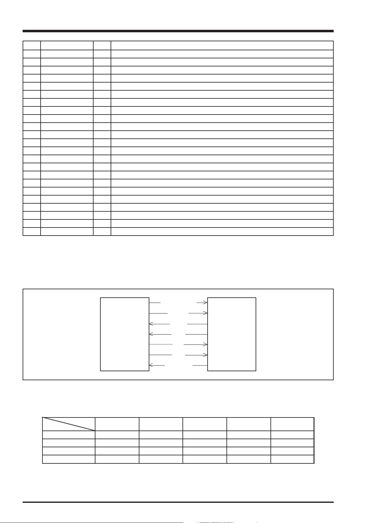
3-5-2. Internal Communications Paths
The SYA block is used for detecting the status of the camera circuits and input from operation keys, and for controlling the
entire camera. The 8-bit microprocessor loads signals from the various detection sensors as input data and then outputs the
results to the camera circuit (ASIC) as operation mode settings data.
Figure 5-1 shows the connections between the 8-bit microprocessor and the ASIC.
MAIN RESET
PLL EN
8-bit
microprocessor
<Fig 3-3. Internal communication path connections>
SREQ
SDO
SDI
SCK
COMREQ
ASIC
3-5-3. Key Operations
Refer to the Instruction Manual for information on how to use the camera’s keys.
SCAN IN
SCAN OUT
0 MOVIE SHUTTER FOCUS PW_TEST TEST
1 MANUAL AUTO SP - 2 PLAY DISP WIDE TELE RIGHT
3 F_MODE LEFT UP OK DOWN
01234
<Table 3-3. Key operations>
26

FinePix F650 Service Manual
3. Schematics
3-5-4. Power Supply Control
An 8-bit microprocessor controls power to the entire system. This description covers the starting and stopping of the power
supply.
When the battery is installed, IC501 is activated and generates 5.0 volts. This power supply is regulated to 3.2 V by IC302 and
supplied to a microprocessor (IC301). Even when the power switch is set to OFF, clock counting and key scanning continues
in readiness for the next activation.
When the power is turned off, the microprocessor stops the main clock (4 MHz) and runs on the sub-clock (32.768 kHz).
When the power is turned off, the supply voltage switching function for the IC302 microprocessor runs the microprocessor in
power-saving mode.
When the battery supplying power is removed, IC302 switches the power supply for the 8-bit microprocessor to the backup
battery and the microprocessor runs in low-power mode. In this situation, the microprocessor stops the main clock and runs
the clock only using the sub-clock used for keeping the time.
(The backup battery is charged for 10 hours after the battery is fitted.) When the power switch is set to ON, the
microprocessor performs activation processing. First, it sets PON (pin 30) to High to activate the power circuit. Roughly 97.6
ms after setting PON to High, it specifies the external port setting for the ASIC. This external port setting is then used to set
the ASIC internal operating frequency and control oscillation. The microprocessor also initiates communication with the ASIC
and checks that the system is capable of running.
When the LCD panel lights, LCDON (pin 42) is set to High and the panel power supply is activated. BLON (pin 43) is then set
to High to activate the backlight power supply.
When the power is turned off, the lens retracts, PON, LCDON and BLON are all set to Low and the power supply to the
system stops. The microprocessor stops main clock oscillation and the operation mode switches to clock oscillation.
ASIC, memory CCD 8bit CPU LCD MONITOR
Power supply voltage 1.2V, 3.25V 12.0V, -7.5V, 3.4V 3.2V 3.0V
At PW_OFF OFF OFF 32KHz OFF
In live image ON ON 4MHz ON
In playback mode ON OFF 4MHz ON
<Table 3-4. Power supply control>
27
 Loading...