

FUJIFILM FinePix F601 SERVICE MANUAL
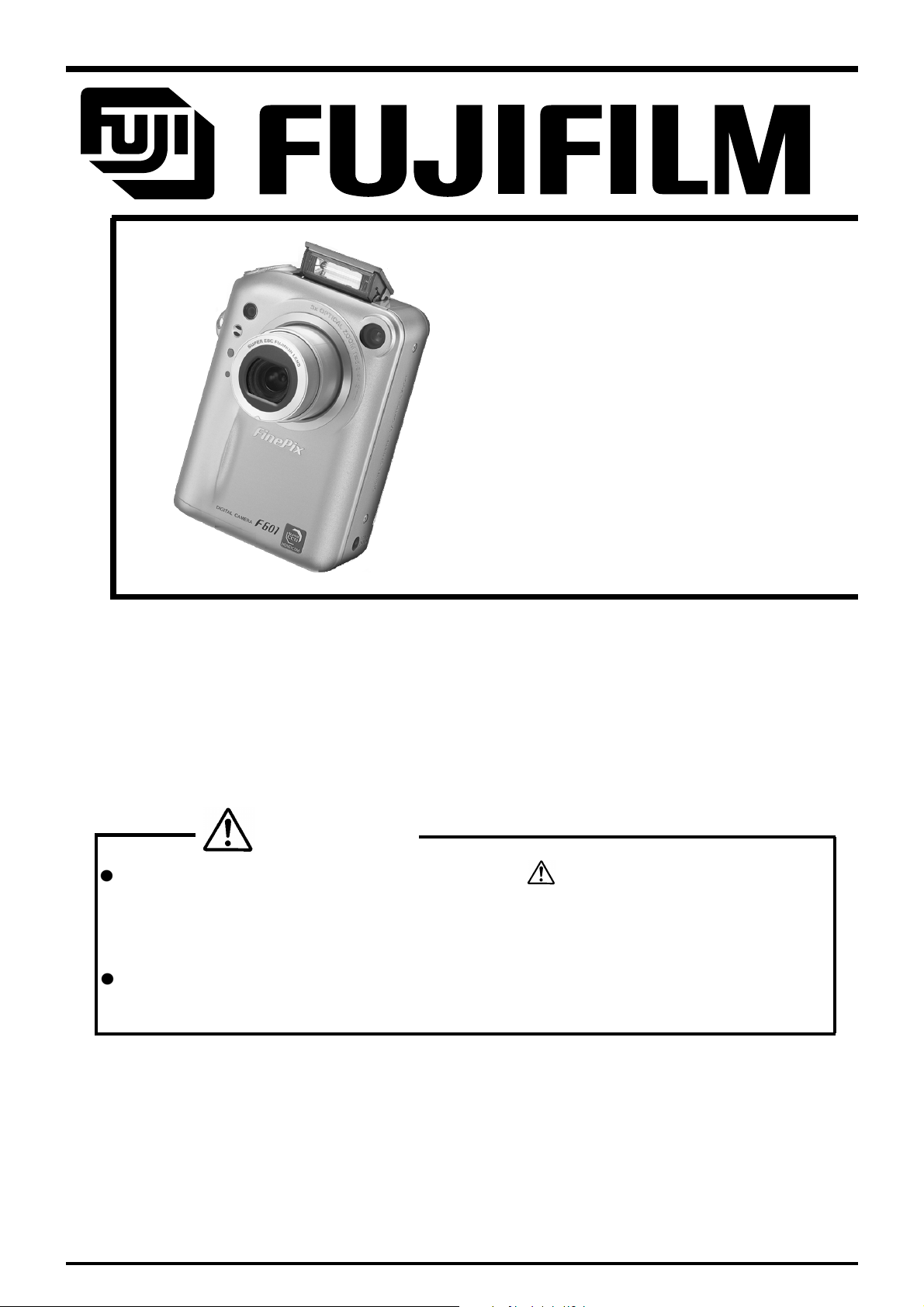
DIGITAL CAMERA
FinePix F601 Zoom
SERVICE MANUAL
U/E/EG-Model
WARNING
THE COMPORNENTS IDENTIFIED BY THE MARK “ “ ON THE SCHEMATHIC
DIAGRAM AND IN THE PARTS LIST ARE CRITICAL FOR SAFETY.
PLEASE REPLACE ONLY BY THE COMPORNENTS SPECIFIED ON THE SCHMATHIC
DIAGRAMAND IN THE PARTS LIST.
IF YOU USE WITH PART NUMBER UN-SPECIFIED, IT MAY RESULT IN A FIRE AND AN
ELECTORICAL SHOCK.
Ref.No.:ZM00430-103
FUJI PHOTO FILM CO.,LTD.
Printed in Japan 2002.2(T.S.)
SAFETY CHECK-OUT
After correcting the original problem, perform the following safety
check before return the product to the costomer.
FinePix F601 Zoom(U/E/EG) SERVICE MANUAL
1. Check the area of your repair for unsoldered or poorly
sol dered connections. Check the entire board sur
face for solder splasher and bridges.
2. Check the interboard wiring to ensure that no wires
are “pinched” or contact high-wattage resistors.
3. Look for unauthorized replacement parts, particu
larly tran sistors, that were installed during a previ
ous repair. Point them out to the customer and rec
ommend their replacement.
4. Look for parts which, though functioning, show obvi
ous signs of deterioration. Point them out to the cus
tomer and recommend their replacement.
5. Check the B + voltage to see it is at the values specified.
6. Make leakage - current measurements to determine
that exposed parts are acceptably insulated from the
supply circuit before returning the product to the customer.
7. CAUTION: FOR CONTINUED
PROTECTION AGAINST FIRE
HAZARD, REPLACE ONLY WITH
SAME TYPE 2.5 AMPERES 125V
FUSE.
2.5A125V
2.5A125V
8.
RISK OF FIREREPLACE FUSE
AS MARKED
WARNING!
HIGH VOLTAGE
ATTENTION: AFIN D'ASSURER
UNE PROTECTION
PERMANENTE CONTRE LES
RISQUES D'INCENDIE,
REMPLACER UNIQUEMENT
PAR UN FUSIBLE DE MEME,
TYPE 2.5 AMPERES, 125
VOLTS.
WARNING:
TO REDUCE THE ELECTRIC
SHOCK, BE CAREFUL TO
TOUCH THE PARTS.

FinePix F601 Zoom(U/E/EG) SERVICE MANUAL
CONTENTS
Table of Contents
1. General
1-1.Product Specifications ..................................................... 4
1-2.Camera Features.............................................................. 6
1-3.Names of External Components .................................... 7
2. Disassembly
2-1.Names of internal Components ...................................... 8
2-2.Removing R PANEL ASSY ............................................. 9
2-3.Removing 8 DIRECTION KEY ASSY/LED PWB ASSY ..... 10
2-4.Removing F PANEL ASSY.............................................. 11
2-5.Removing BARRIER MOTOR HEAD ............................. 12
2-6.Removing MODE ST UNIT.............................................. 13
2-7.Removing LENS CONST ................................................. 13
2-8.Removing SUB PWB ASSY ............................................ 14
2-9.Removing MAIN PWB ASSY .......................................... 14
2-10.Removing BATTERY LID ASSY................................... 15
2-11.Removing DC PWB UNIT ............................................. 15
2-12.Removing LCD................................................................ 16
2-13.Removing STRUCTURE ASSY .................................... 16
Page
Page
4-9.Adjustment Software Initial Setup ................................. 29
4-10.Starting the Adjustment Software ................................ 31
4-11.[F1]: Battery Voltage Adjustment................................. 32
4-12.[F2]: Mode Dial Voltage Adjustment ........................... 34
4-13.[F4]: CCD Defect Correction Adjustment ................... 35
4-14.[F5]:CAM adjustment ..................................................... 36
4-15.[F6]: AF Adjustment ....................................................... 38
4-16.[F7]: Flash Adjustment .................................................. 40
4-17.[F9]: DC Jack Voltage Adjustment ..............................41
4-18.[F11]: Product Model Check ......................................... 42
4-19.[F12]: End Setting .......................................................... 43
5. Inspection
5-1.Measuring Instruments and Jigs Used for Inspection ........ 45
5-2.Connection of Measuring Instruments for Inspection ......... 45
5-3.Inspection and Settings at Shipment ............................ 45
5-4.Inspecting Resolution ...................................................... 49
5-4-1.Settings and Photography for Inspecting
Resolution ......................................................................... 49
5-4-2.Checking Resolution ............................................. 51
3. Schematic
3-1.Cautions ............................................................................. 17
3-2.Basic block name and function explanation ................. 17
3-3.Primary Block Functions Description ............................ 18
3-3-1.Technical Outline .................................................. 18
3-3-2.Block Functions Descriptions .............................. 18
3-4.Basic block diagram......................................................... 19
3-5.Overall Connections......................................................... 20
3-6.Board mounting diagram ................................................. 21
3-6-1.Printed wiring board of DC PWB UNIT .............. 21
3-6-2.Printed wiring board of MAIN PWB ASSY......... 22
3-6-3.Printed wiring board of SUB PWB ASSY .......... 23
3-6-4.Printed wiring board of LED PWB ASSY ........... 23
4. Adjustment
4-1.Adjustments After Replacing Major Components ........ 24
4-2.Procedures for Adjustments After Replacing Major
Components ...................................................................... 24
4-3.Measuring Instruments Used.......................................... 24
4-4.Jigs Used ........................................................................... 24
4-5.Jig Connection .................................................................. 25
4-6.Setup for adjustment ....................................................... 25
4-7.Various downloading software decompressions,
preservation methods, and notes ................................. 26
4-8.Install the DSC jig driver and the PC adjustment
software ............................................................................ 28
6. Parts List
6-1.Packing and Accessories ................................................ 52
6-1-1.U-MODEL ............................................................... 52
6-1-2.E-MODEL ............................................................... 53
6-1-3.EG-MODEL ............................................................ 54
6-2.Cabinet F ........................................................................... 55
6-2-1.Cabinet F (U-Model) ............................................. 55
6-2-2.Cabinet F (E/EG-Model) ....................................... 56
6-3.Internal parts ..................................................................... 57
6-3-1.Internal parts (U-Model) ....................................... 57
6-3-2.Internal parts (E/EG-Model) ................................ 58
6-4.Cabinet R (U/E/EG-Model commonness) ..................... 59
6-5.Electrical Parts (U/E/EG-Model commonness) ............ 60
7. Appendix
7-1.Preparing the CCD Defect Data Floppy Disk ............... 61
7-2.List of Related Technical Updates Issued .................... 62
8. Downloading Firmware
8-1. Setting up the Downloading Software .......................... 63
8-2. [F8] Firmware Download ................................................ 63
Revised:01.Apr.2002
3
1.General
FinePix F601 Zoom (U/E/EG) SERVICE MANUAL
1.General
1-1. Product specification
System
Model Digital camera FinePix F601 ZOOM
Number of effective pixels
CCD sensor 1/1.7-inch Super CCD in an interwoven pattern
Image file size 2832 × 2128 pixels (6.03 million pixels) / 2048 × 1536 pixels / 1280 × 960 pixels /
File format Still image: JPEG (Design rule for Camera File System compliant), DPOF compatible
Storage media SmartMedia (3.3V)
Viewfinder Real image optical
Lens Super EBC Fujinon optical 3´ zoom lens
Aperture F2.8-F4.5/F4.0-F6.3/F5.6-F8.8/F8.0-F12.4 (automatically selected)
Focus TTL contrast-type, Auto or Manual
Focus distance f = 8.3 mm-24.9 mm (Equivalent to 36 mm-108 mm on a 35 mm camera)
3.1million pixels
Number of total pixels 3.3 million pixels
640 × 480 pixels
Movie: AVI format, Motion JPEG
Audio: WAV format
Standard number of shots per SmartMedia™
File Size 2832 × 2128 2048 × 1536
Quality Mode FINE
Image Data Size
MG-4S (MG-4MB)
MG-8S (MG-8MB)
MG-16S (MG-16MB)
MG-32S (MG-32MB)
MG-64S (MG-64MB)
MG-128S (MG-128MB)
Exposure control TTL 64-zones metering, Program AE ( n n n n ), exposure compensation available
Sensitivity Equivalent to ISO 160/200/400/800/1600
White balance Auto (In Manual modes, 7 positions can be selected.)
Focal range Normal: Approx. 60 cm (2.0 ft.) to infinity
Shutter Variable-speed, 3 sec. to 1/2000 sec. (depend on Exposure mode)
Flash Auto flash using flash control sensor
Erase modes ERASE FRAME, ERASE ALL FRAMES, FORMAT (initialize)
LCD monitor 1.5-inches, low-temperature polysilicon TFT 110,000 pixels
Video output NTSC (U.S.A./Canada model) / PAL (Europe model)
Self-Timer 10 sec. timer clock
Approx. Approx. Approx. Approx. Approx. Approx. Approx. Approx.
2400KB 1200KB 460KB 1300KB 590KB 620KB 320KB 130KB - - -
NORMAL BASIC
1382661230
3 6 17 6 13122561
6 133312262549122
13 28 68 25 53 50 99 247
26 56 137 50 107 101 198 497
53 113 275 102 215 204 398 997
in Manual photography mode
Macro : Approx. 20 cm (0.7 ft.) to 80 cm (2.6 ft.)
Effective range: Wide-angle Approx. 0.2 m-4.7 m (7.8 in.-15.4 ft.)
Telephoto Approx. 0.2 m-3 m (7.8 in.-9.8 ft.)
Flash modes: Auto, Red-Eye Reduction, Forced Flash, Slow Synchro
FINE
NORMAL
1280 × 960
FINE
640 × 480
NORMAL NORMAL
Movie (Video)
VGA QVGA -
Approx.6sec. Approx.16sec. Approx.8sec.
Approx.13sec. Approx.33sec. Approx.16sec.
Approx.27sec. Approx.66sec. Approx.33sec.
Approx.55sec. Approx.135sec. Approx.67sec.
Approx.111sec. Approx.271sec. Approx.135sec.
Approx.223sec. Approx.544sec. Approx.272sec.
Audio recording
Input/Output Terminals
DC Input To connect the AC power Adapter AC-5VS/AC-5VHS
Cradle connection socket Connects to the optional cradle
4

FinePix F601 Zoom (U/E/EG) SERVICE MANUAL
Power Supply and Others
Power supply Use one of the following
n
Rechargeable Battery NP-60 or AC Power Adapter AC-5VS/AC-5VHS
Available shots / Battery Type No. of Shots Audio Recording
time using the battery
(When fully charged) LCD moniter OFF Approx.300 Approx.4 hour
LCD moniter ON Approx.150 Approx.2 hour
NP-60
The number of shots shown here is an approximate guide to the number of consecutive
shots that can be taken based on 50% flash usage at normal temperatures. However, the
actual number of available shots will vary depending on the ambient temperature when
the camera is used and the amount of charge in the battery. The number of available
shots or available shooting time will be lower in cold conditions.
1.General
Conditions for use Temperature: 0
o
C to +40oC (+32oF to +104oF)
80% humidity or less (no condensation)
Camera dimensions 72.0 mm × 93.0 mm × 34.0 mm / 2.8 in. × 3.7 in. × 1.3 in.
(W/H/D) (not including accessories and attachments)
Camera mass (weight) 220 g / 7.8 oz. (not including accessories, batteries or SmartMedia)
Weight for photography Approx. 250 g / 8.8 oz. (including batteries and SmartMedia)
Accessories
n SmartMedia (16MB, 3.3V) (1)
Supplied with:
nAnti-static case (1)
n
Index label (1)
n NP-60 Rechargeable Battery (1)
Soft case included
n Strap (1)
n AC-5VS/AC-5VHS AC Power Adapter (1)
Approx. 2 m (6.6 ft.) connection cord
n USB Interface Set (1)
n
CD-ROM: Software for FinePix EX (1)
n
FinePix F601 ZOOM Special USB cable with Noise Suppression core (1)
n
Software Quick Start Guide (1)
n Owner’s Manual (1)
Optional Accessories
n SmartMedia™
MG-4S: 4MB, 3.3V MG-8S: 8MB, 3.3V MG-16S/SW: 16MB, 3.3V
MG-32S/SW: 32MB, 3.3V MG-64S/SW: 64MB, 3.3V
n BC-60 Battery Charger
n NP-60 Rechargeable Battery
n AC-5VH/AC-5VHS AC Power Adapter
n PictureCradle CP-FX601
n SC-FX601 Soft Case
n FD-A2 Floppy Disk Adapter (FlashPath)
Windows 95/98/98 SE/Me/NT4.0, Mac OS 7.6.1 to 9.1
n SM-R2 Image Memory Card Reader
Compatible with Windows 98/98 SE, Windows Me, Windows 2000 Professional or iMac
and models that support USB as standard.
n DM-R1 Image Memory Card Reader
Compatible with Windows 98 SE, Windows 2000 Professional (read-only), iMac DV
and Power Macintosh PCs with FireWire as a standard feature. Mac OS 8.5.1 to 9.1
n PC-AD3 PC Card Adapter
5

1.General
FinePix F601 Zoom (U/E/EG) SERVICE MANUAL
1-2.Camera Features
n 3.1 million effective pixels.
n 2832 x 2128 (6.03 million) recorded pixels Built-in 3 x zoom lens with a low-dispersion aspherical lens for
superb optical performance.
n Compact and lightweight aluminum-magnesium alloy body.
n Quick, responsive operation with 2-second startup and as little as 1 second between shots.
n Auto focus with macro function (manual focus also available).
n Automatic shooting modes that can be tailored to subjects in different photography conditions.
n Shutter-priority AE, Aperture-priority AE and Manual exposure functions.
n High-sensitivity photography (1M mode only).
n Convenient preview function for quickly checking of your shots.
n The 6.6× Honeycom zoom lens makes the most of the Super CCD Honeycom features (3× optical zoom coupled
with a superbly smooth (multi-level) digital zoom function offering up to 2.2× zooming at megapixel resolutions).
n Playback zoom function (up to 18x).
n Continuous shooting function.
n Movie shooting function (640 × 480/320 × 240 pixels with sound).
n Voice Memo function for easy photography information recording.
n Audio Recording function.
n 1.5-inches 110,000-pixels low-temperature polysilicon TFT LCD monitor.
n Recharge or connect to your PC simply by placing the FinePix F601 ZOOM in its cradle (sold separately).
n Easy high-speed image file transfer via the USB connection.
n Conforms to the new standard for digital camera file system*.
* Design rule for Camera File System
Explanation of Terms
DPOF: Digital Print Order Format
DPOF is a format used for recording information on a storage media (image memory
card, etc.) that allows you to specify which of the frames shot using a digital camera
are printed and how many prints are made of each image.
EV: A number that denotes exposure. The EV is determined by the brightness of the
subject and sensitivity (speed) of the film or CCD. The number is larger for bright
subjects and smaller for dark subjects. As the brightness of the subject changes, a
digital camera maintains the amount of light hitting the CCD at a constant level by
adjusting the aperture and shutter speed. When the amount of light striking the CCD
doubles, the EV increases by 1. Likewise, when the light is halved, the EV decreases
by 1.
JPEG: Joint Photographics Experts Group
A file format used for compressing and saving color images. The compression ratio
can be selected, but the higher the compression ratio, the poorer the quality of the
expanded image.
Motion JPEG: A type of AVI (Audio Video Interleave) file format that handles images and sound as a
single file. Images in the file are recorded in JPEG format. Motion JPEG can be played
back by QuickTime 3.0 or later.
PC Card: A generic term for cards that meet the PC Card Standard.
PC Card Standard: A standard for PC cards determined by the PCMCIA.
PCMCIA: Personal Computer Memory Card International Association (US).
White Balance: Whatever the kind of the light, the human eye adapts to it so that a white object still
looks white. On the other hand, devices such as digital cameras see a white subject
as white by first adjusting the color balance to suit the color of the ambient light around
the subject. This adjustment is called matching the white balance. A function that
automatically matches the white balance is called an Automatic White Balance function.
6
FinePix F601 Zoom (U/E/EG) SERVICE MANUAL
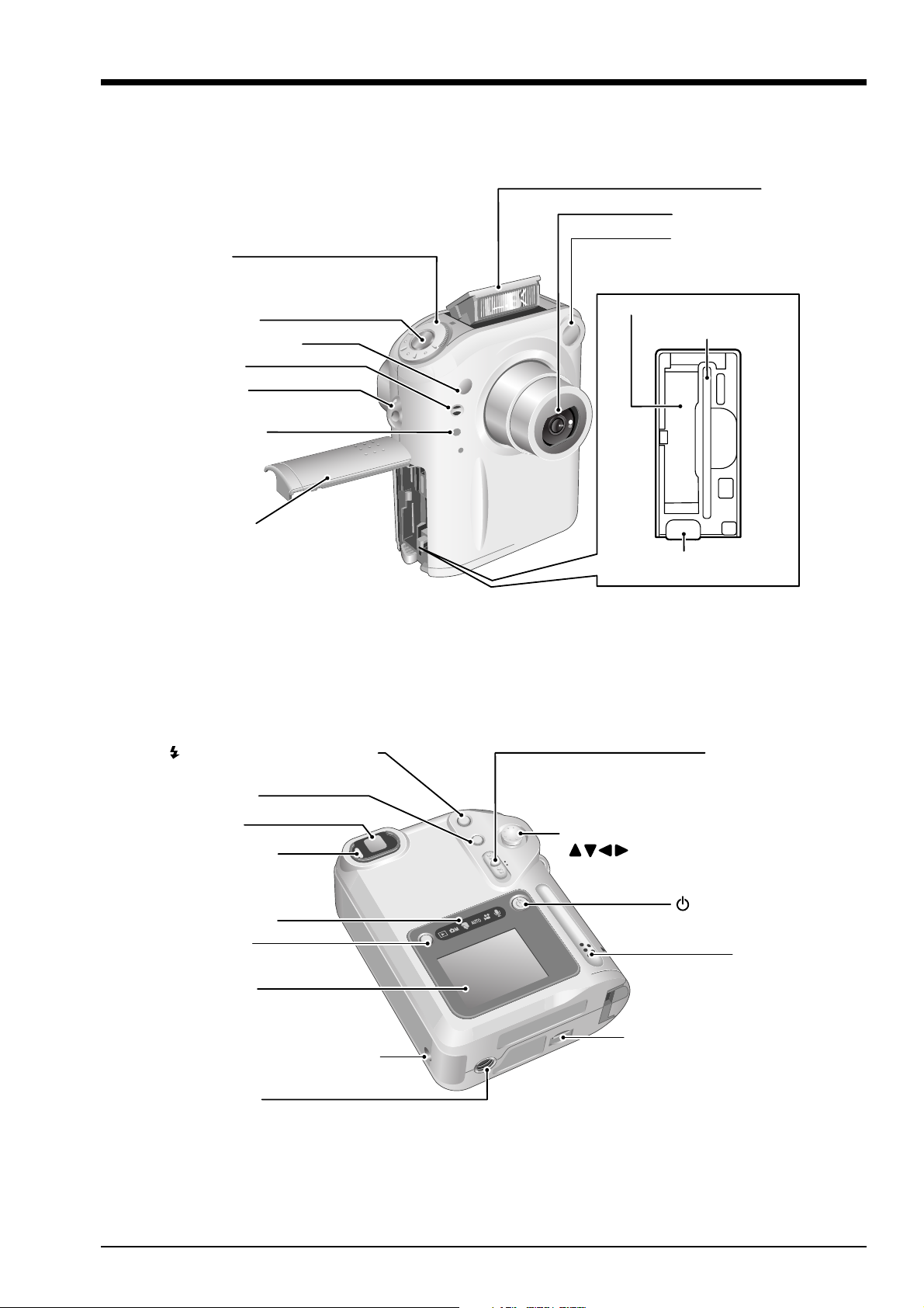
1-3.Names of External Components
Mode dial
1.General
Flash
Lens / Lens Cover
Viewfinder window
Shutter button
Flash control sensor
Microphone
Strap mount
Self-timer lamp
Battery cover
OPEN (Flash pop-up) button
Battery compartment
SmartMedia slot
Battery lock release button
Mode switch
BACK button
Viewfinder
Viewfinder lamp
Mode indicators
DISP button
LCD monitor
DC IN 5V (Power input) socket
Tripod mount
Multifunction
( and MENU/OK ) button
(Power) button
Speaker
Connection socket /
Connection socket cover
7
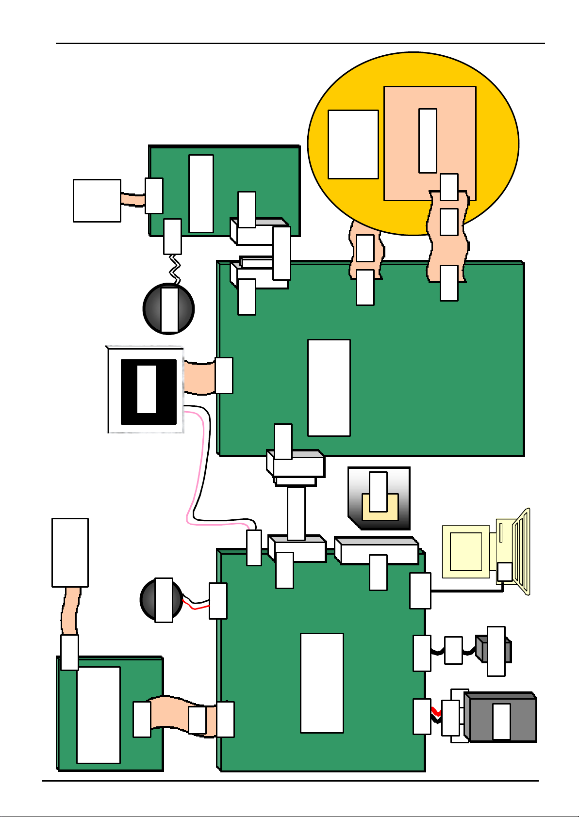
2. Disassembly
2. Disassembly
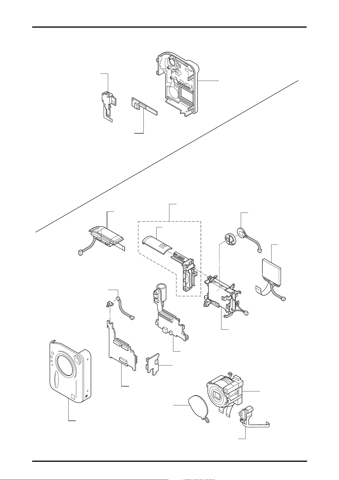
2-1.Names of internal Components
8 DIRECTION KEY ASSY
LED PWB ASSY
FinePix F601 Zoom (U/E/EG) SERVICE MANUAL
R PANEL ASSY
MIC ASSY
MODE ST UNIT
BATTERY LID ASSY
SPEAKER ASSY
BATTERY LID
LCD
STRUCTURE ASSY
DCST PWB UNIT
SUB PWB ASSY
MAIN PWB ASSY
LENS BARRIER
F PANEL ASSY
BARRIER MOTOR HEAD
LENS CONST
8
FinePix F601 Zoom (U/E/EG) SERVICE MANUAL
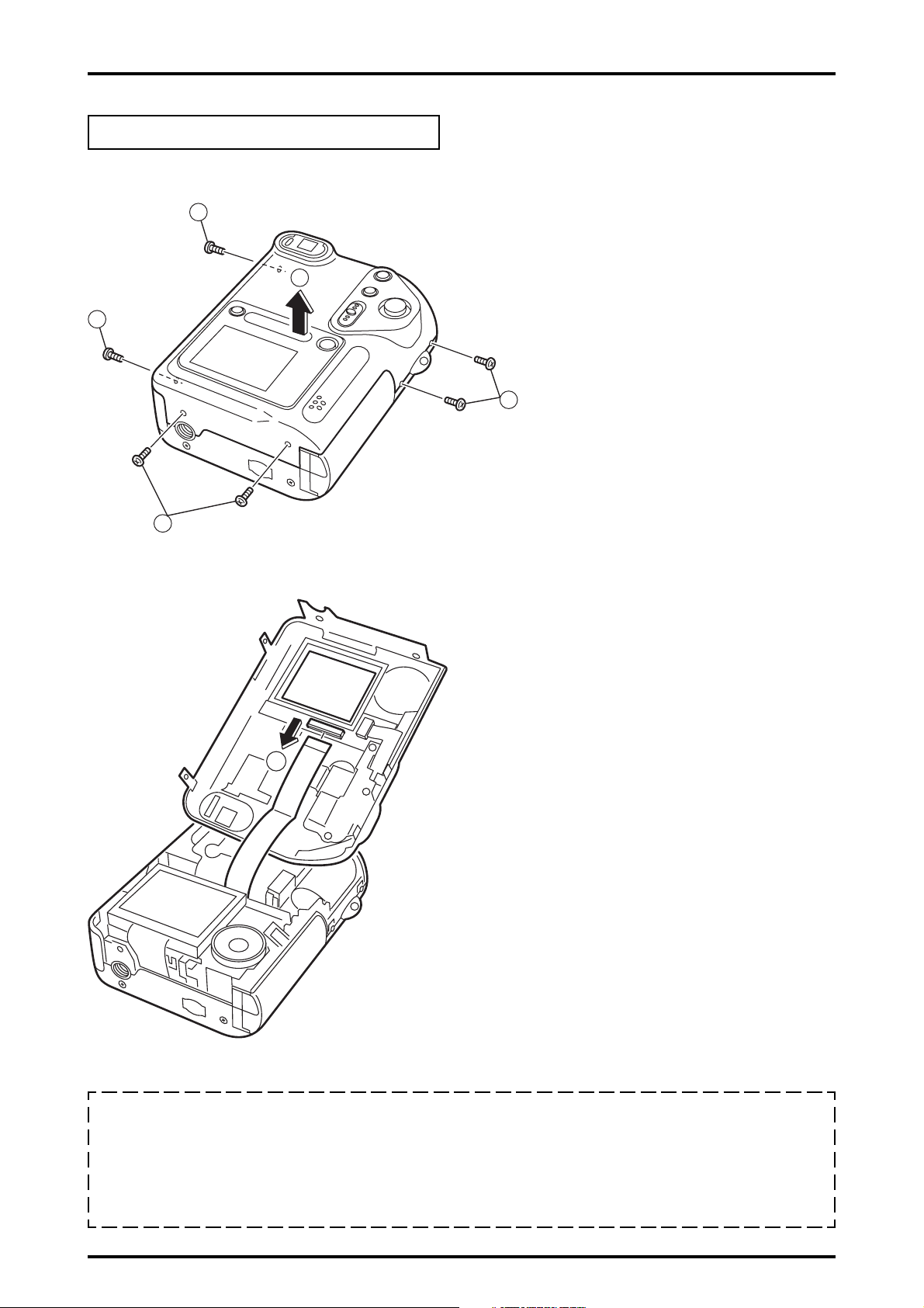
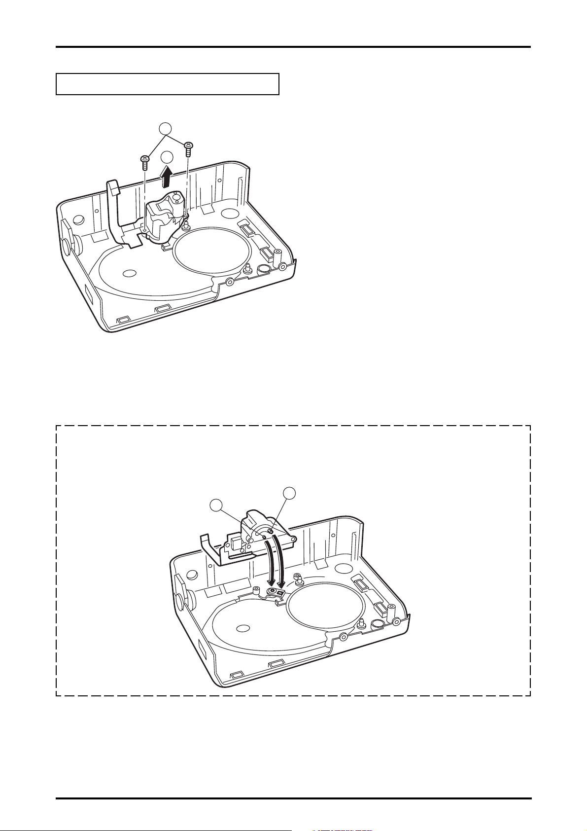
2-2.Removing R PANEL ASSY
Remove in the order indicated by circled numbers.
<Step 1>
2. Disassembly
2
<Step 2>
2
3
1
(1) Remove four screws(BB12585-100).
(2) Remove two screws(BB12489-200).
(3) Remove R PANEL ASSY(BU01937-100) in the
direction of the arrow.
1
(4) Remove the lock of connector (CN52),
and remove FPC(FZ04383-100).
4
[ Notes of assembly of R PANEL ASSY. ]
1. Assemble BATTERY LID with the closed state.
2. Lock connector (CN52) surely. Moreover, prevent "Diagonal insertion and insertion of the half" of FPC from being.
3. Confirm there is no space when "F PANEL ASSY" and "R PANEL ASSY" are combined, and the screw is tightened.
9
2. Disassembly
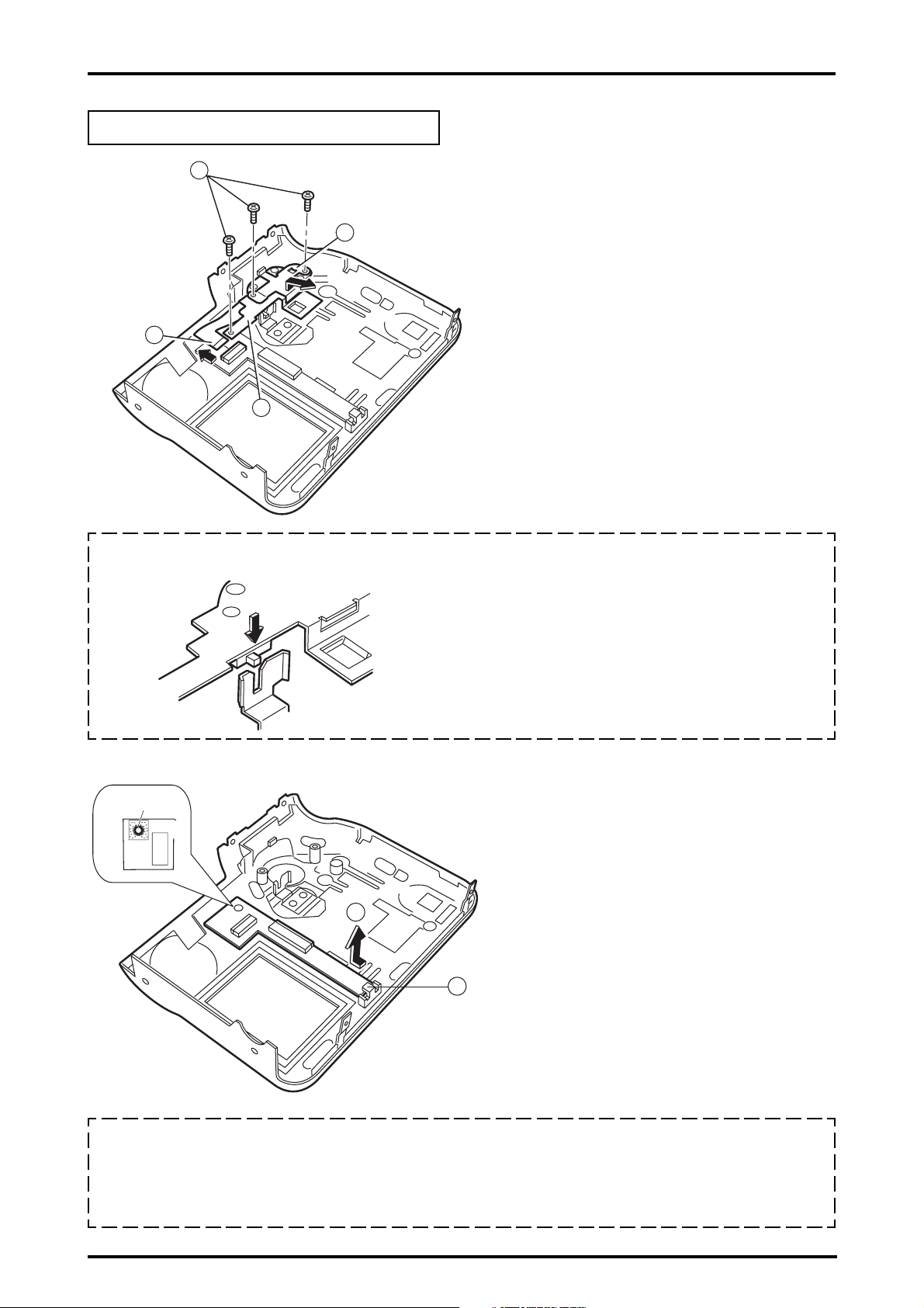
2-3.Removing 8 DIRECTION KEY ASSY/LED PWB ASSY.
Remove in the order indicated by circled numbers.
FinePix F601 Zoom (U/E/EG) SERVICE MANUAL
<Step 1>
1
3
2
4
[ Notes of assembly of 8 DIRECTION KEY ASSY.]
(1) Remove three screws(ATG1723-5ND).
(2) Remove the lock of connector (CN51),
and remove FPC of 8 DIRECTION KEY ASSY.
(3) Remove 8 PLATE(BB13061-100) in the
direction of the arrow.
(4) Remove 8 DIRECTION KEY ASSY(FZ04349-100)
in the direction of the arrow.
<Step 2>
Step boss
* Note the combination of MODE PLATE and the slide
switch when you build in 8 DIRECTION KEY ASSY.
(5) Remove LED PWB ASSY(CB0840-A200) in
the direction of the arrow.
CN51
5
A
[ Notes of assembly of LED PWB ASSY. ]
1. Set LED PWB ASSY in the hook and, put LED PWB ASSY under of the step boss.
2. Lock connector (CN51) surely. Moreover, prevent "Diagonal insertion and insertion of the half" of FPC from being.
10
FinePix F601 Zoom (U/E/EG) SERVICE MANUAL
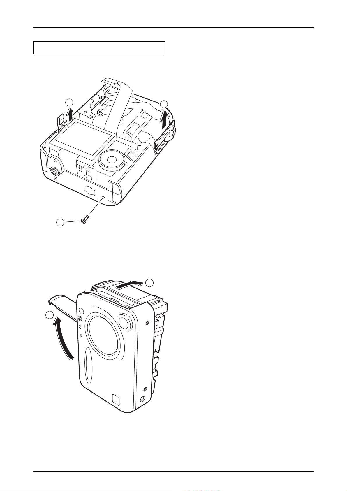
2-4.Removing F PANEL ASSY.
Remove in the order indicated by circled numbers.
<Step1>
3
2. Disassembly
(1) Remove one screw(BB12585-100).
(2) Remove STRAP METAL(BB13058-100) in the
direction of the arrow.
2
(3) Remove FPC of BARRIER MORTOR HEAD in
the direction of the arrow.
[ = Pull out FPC from connector (CN151). ]
<Step 2>
4
1
5
(4) Open BATTERY LID(BB13042-100) in the
direction of the arrow.
(5) Remove the entire internal part in the direction
of the arrow.
11
2. Disassembly
2-5.Removing BARRIER MOTOR HEAD.
Remove in the order indicated by circled numbers.
<Step 1>
1
2
FinePix F601 Zoom (U/E/EG) SERVICE MANUAL
(1) Remove two screws(ATG1722-0ND).
(2) Remove BARRIER MOTOR HEAD
(FZ04321-100) in the direction of the arrow.
[ Notes of assembly of BARRIER MOTOR HEAD. ]
* When you combine BARRIER MOTOR HEAD with F PANEL ASSY, shut LENS BARRIER and combine
"Barrier drive shaft (A) of BARRIER MOTOR HEAD" and "Hole site of LENS BARRIER(B)".
A
B
12
FinePix F601 Zoom (U/E/EG) SERVICE MANUAL
2-6.Removing MODE ST UNIT.
Remove in the order indicated by circled numbers.
<Step 1>
4
1
2
6
2. Disassembly
(1) Remove the lock of connector (CN11), and
remove FPC of MODE ST UNIT(BF03674-100).
(2) Remove pop up switch (SW11).
7
UL tape
3
(3) Remove ST SHEET(BB13063-100).
(4) Remove the hook of LENS CONST (two places).
5
(5) Do discharge of the flash.
(6) Remove the lock of connector (CN801), and
remove the connector of MODE ST UNIT.
(7) Remove MODE ST UNIT.
[ Notes of assembly of MODE ST UNIT. ]
1. Do the work of decomposition and assembly so that strong power should not hang in connector (CN11)
which has been inserted in LENS CONST. When work that strong power hangs is done, the case where the
solder of connector (CN11) and HONEYCOM CCD peels off is the worst case.
2. Make the straight line part of FPC of MODE ST UNIT a standard, and attach the UL tape on ST SHEET.
2-7.Removing LENS CONST .
Remove in the order indicated by circled numbers.
<Step 1>
(1) Remove connector (CN102/CN103), and
2
remove FPC of LENS CONST(BU01983-100).
(2) Remove LENS CONST in the direction of the arrow.
1
1
[ Notes of assembly of LENS CONST. ]
1. Insert the hook of "2-6.(4)" in two places surely.
2. Lock connector (CN102 and CN103) surely.
Moreover, prevent "Diagonal insertion and insertion
of the half" of FPC from being.
13
2. Disassembly
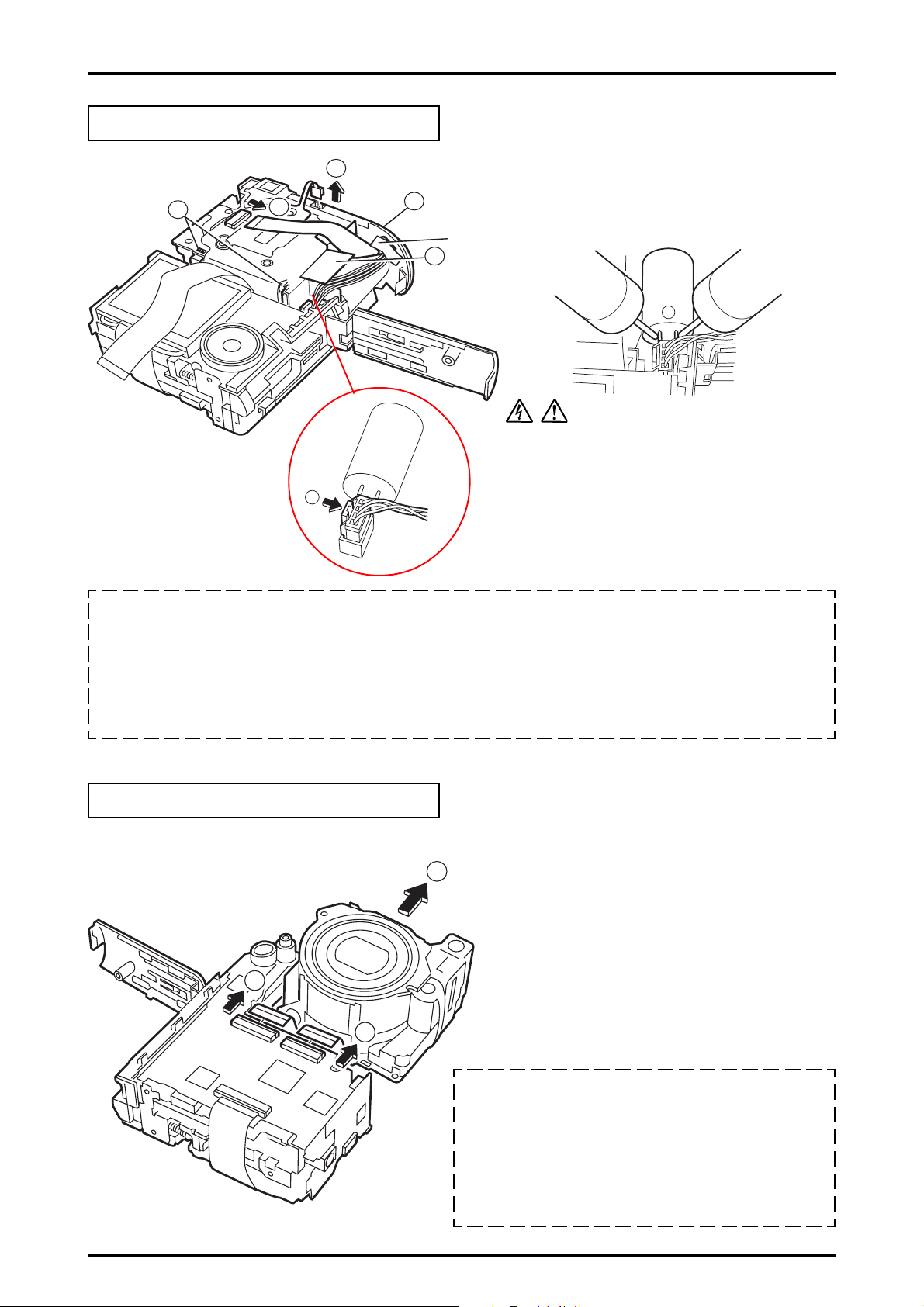
2-8.Removing SUB PWB ASSY.
Remove in the order indicated by circled numbers.
<Step 1>
FinePix F601 Zoom (U/E/EG) SERVICE MANUAL
(1) Remove the connector of MIC ASSY(FZ04380-100).
(2) Remove "Board to board" connector (CN152) of
SUB PWB ASSY(CB0840-A100) in the direction
of the arrow, and remove SUB PWB ASSY.
1
2
2-9.Removing MAIN PWB ASSY.
Remove in the order indicated by circled numbers.
<Step 1>
3
2
(1) Remove one screws(BB11640-100).
(2) Remove the lock of connector (CN551), and
1
remove FPC of LCD.
(3) Remove MAIN PWB ASSY in the
direction of the arrow.
14
CN202
IC356
IC353
F351
IC204
CN101
IC206
IC208
IC202
SHEET STROBE
[ Notes of assembly of MAIN PWB ASSY. ]
1.Stop the harness of MIC ASSY by drawing around
SHEET STROBE(BB14127-100) as shown in a left chart.
2. Be note not to pinch the harness when you combine
MAIN PWB ASSY with DCST PWB UNIT and,
note the installation position to MAIN FRAME.
FinePix F601 Zoom (U/E/EG) SERVICE MANUAL
2-10.Removing BATTERY LID ASSY.
Remove in the order indicated by circled numbers.
2. Disassembly
<Step 1>
1
2
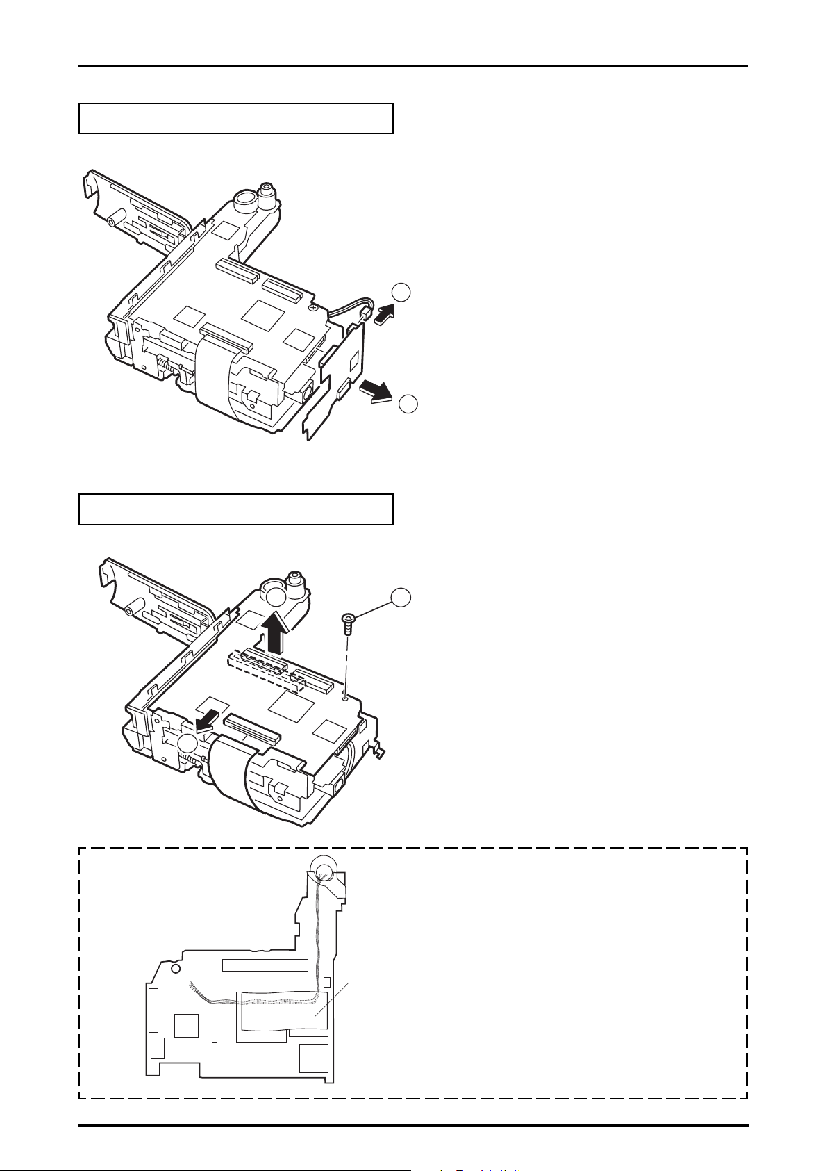
2-11.Removing DC PWB UNIT.
Remove in the order indicated by circled numbers.
<Step 1>
(1) Remove the hook.
(2) Remove BATTERY LID ASSY(BU01939-100)
in the direction of the arrow.
[ Notes of assembly of BATTERY LID ASSY ]
* Fix an upper hook after putting a lower hook.
(1) Remove one screws(BB11640-100).
1
3
2
2
2
[ Notes of assembly of DC PWB UNIT ]
1. Form the harness of BATTERY CONNECTOR ASSY referring to a left
photograph.Make the overlapping of the harness only "red and white"
and, form a red harness to FRAME(A part).
2. Be note not to pinch the harness when you combine DC PWB UNIT
with MAIN FRAME and, note the installation position to MAIN FRAME.
(2) Remove the connector of LCD.
[ = Pull out connector (CN603). ]
Remove the connector of
BATTERY CONNECTOR ASSY(FZ04374-100).
[ = Pull out connector (CN602). ]
Remove the connector of
SPEAKER ASSY(FZ04652-100).
[ = Pull out connector (CN606). ]
(3) Remove DC PWB UNIT(BF03684-100)
in the direction of the arrow.
FRAME(A part)
Red harness
15

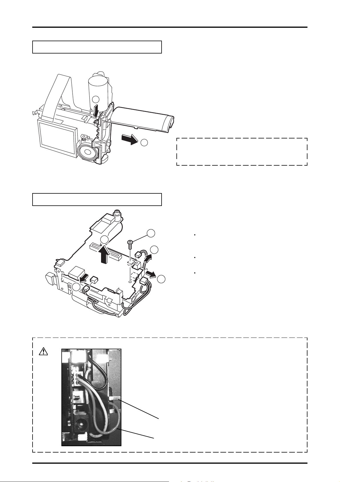
2. Disassembly
2-12.Removing LCD.
Remove in the order indicated by circled numbers.
<Step 1>
2
1
1
FinePix F601 Zoom (U/E/EG) SERVICE MANUAL
(1) Remove the hook two places.
(2) Remove LCD(FZ04408-100) in the direction
of the arrow.
[ Notes of assembly of LCD. ]
1. Put LCD in a right hook. Afterwards, put a left hook.
2. Lock connector (CN551) surely. Moreover,
prevent "Diagonal insertion and insertion of the
half" of FPC from being.
2-13.Removing STRUCTURE ASSY.
Remove in the order indicated by circled numbers.
<Step 1>
1
3
3
<Step 2>
(1) Remove one screw(BB11384-100).
(2) Remove SUB FRAME(BB13091-100).
(3) Remove the hook three places.
2
(4) Remove BATT FLAME ASSY(BU01940-100)
in the direction of the arrow.
16
4
[ Notes of assembly of STRUCTURE ASSY. ]
1. Do not pinch the harness of BATTERY CONNEC-
TOR ASSY.

FinePix F601 Zoom (U/E/EG) SERVICE MANUAL
3.Schematic
3.Schematic
3-1.Cautions
<Caution when replaceing chip (leadless) parts.>
* Do not re-use the removed parts, but use new parts.
Be careful that the negativ side of the tantalum capacitors are susceptible to heat.
* Voltage indications are omitted for capacitors other than chemical and tantalum capacitors
with a dielectric strength of 50 V or less.All units are uF (p shows pF).
* Chip resistors without indication are 1/10 W.
* k=1000
* Variable resistors and semi-variable resistor are abbreviated the specification of B characteristic.
3-2.Basic block name and function explanation
Board Name Block name Function
LENS CONST CCD BLOCK * CCD output
MAIN PWB ASSY CAM BLOCK * Analog to digital conversion of CCD output (IC109)
DC PWB UNIT DC/DC BLOCK * Each power supply generation (IC603)
SUB PWB ASSY AUDIO BLOCK * Audio signal processing (IC401)
LED PWB ASSY LED BLOCK * LED, Operation SW(ON<--->OFF/ display/ )
MODE ST UNIT MRSW BLOCK * Flash luminescence, Mode SW (mode)
8 KEY KEY BLOCK * Operation SW( CAM<->PB//U<->D/cancellation/L<->R/OK)
, M=1000 k
* CCD driver (IC105)
MOTOR BLOCK * Zoom/AF/shutter/iris drive (IC113/101)
PROCESS BLOCK * Video signal processing (IC204)
* USB communication (IC204)
* System control/SW detection management (IC204)
POWER ON BLOCK * Power supply management(POWER_ON_IC353)
LCD BLOCK * LCD control (IC553)
BL BLOCK * LCD backlight supply (IC603)
FLASH BLOCK * Flash luminescence processing
17

3.Schematic
FinePix F601 Zoom (U/E/EG) SERVICE MANUAL
3-3. Primary Block Functions Description
3-3-1. Technical Outline
The FinePix F601 incorporates a 3rd generation Super CCD Honeycomb and a new signal processing LSI (UCS,
IC204). The signal processing LSI (UCS, IC204) is equivalent to the image signal processing IC (SCS3D, IC304,
CSP) incorporated in the previous FinePix6800Z, however the new IC permits a dramatic reduction in the interval
between photography and playback. Pixel addition processing*1 and noise reduction have produced the world’s
first compact camera capable of photography at ISO800/1600, and the camera also employs the ultra highsensitivity ‘candlelight shot’ useful in scenes at low light levels.
The 3rd generation Super CCD Honeycomb improves performance during movie photography. The new data
transfer method used permits mixing*2 of horizontal and vertical pixels inside the CCD to allow a VGA15 frame
in excess of three megapixels per second, a capability not supported in conventional cameras.
*1 Data obtained with honeycomb signal processing consists of approximately twice the effective number of pixels.
Every four of the pixels is consolidated into a single pixel to increase the signal level (sensitivity) by a factor of four, and
the S/N (signal to noise) ratio by a factor of two, and thus permit photography at up to ISO1600.
*2 Every two pixels on the vertical and horizontal axes of the CCD are mixed to increase the signal level by a factor of four,
and the S/N ratio by a factor of two. This produces movie images of high sensitivity and high quality, while at the same
time permitting high-speed retrieval, and allowing 30 VGA-size frames per second.
3-3-2. Block Functions Descriptions
(1) CCD block (CCD signal processing) and CAM block (image circuit block)
g The analog video signal from the CCD (1" x 1.7", 3,100,000 effective pixels, square pixel honeycomb array, primary
color CCD) is psuedo-color compensated (CDS), adaptively interpolated (CDS), amplified (AGC), and signals mixed
(CDS) in the single-chip CSP IC (SCS3A, IC109), and converted (A/D) to a 12-bit digital signal (CSP IC - Chip Size
Package IC). The CSP IC also incorporates the TG/SSG function previously supported by a separate IC. The converted digital signal is sent to the signal processing LSI (UCS, IC204).
g This block also incorporates the CCD horizontal/vertical drive IC (IC105).
(2) Motor Block
g The signal processing LSI (UCS, IC204) receives commands from the switches, monitors the AF motor drive, shutter
drive, zoom motor drive, and iris motor drive (IC113), and controls each motor with the appropriate driver circuit.
(3) Process Block (image processing)
g Input data from CCD
The 12-bit digital image data (1H equivalent) from the CCD CAM block is sent to the signal processing LSI (UCS,
IC204), buffered in its internal buffer, and converted to 32-bit (16-bit x 2) data (CCD raw data). The 32-bit image data
(CCD raw data) is passed to the 32Mbyte SDRAM (IC206) via the I/O bus in the image signal processing IC. The
SDRAM temporarily stores a single frame equivalent (2832 pixels x 2128 lines). The 32-bit image data input to the
signal processing LSI (UCS, IC204) is processed in the AUTO math processing block and sent to the SCS3A IC
(IC109) in the CAM block to obtain the appropriate AE, AWB, and AF.
g Recording to SSFDC
The image data stored in the SDRAM (IC206) is passed one line at a time to the signal processing block via the I/O
bus in the signal processing LSI (UCS, IC204). This data is unpacked (pre-processing consisting of conversion of 32bit data to 12-bit, digital clampimg, gamma compensation, and conversion of 12-bit R, G, and B data to 8-bit R, G, and
B data, followed by YC processing consisting of conversion of 8-bit digital R, B, and G signals to Y:Cb:Cr=4:2:2) in the
signal processing block, and 8-bit Y, Cr, and B image data is again sent to the internal buffer. The 8-bit Y:Cb:Cr
signals are sorted in the internal buffer into a format to suitable for DCT compression, and sent to the media controller
via the JPEG math block, and recorded in the SSFDC.
g Image playback from SSFDC
The compressed image data from the SSFDC is sent to the signal processing LSI (UCS, IC204) as 8-bit image data
and sent to the SDRAM (IC206) via the media control unit, the DMA unit, and the internal bus control unit. The image
data temporarily stored in the SDRAM (IC206) is returned to the signal processing LSI (UCS, IC204) and sent to the
signal processing block via the media controller and JPEG math block. Post-processing involves conversion of the 8bit Y:Cr:Cb image signals to 8-bit R, G, and B signals in the image processing block, the text display signal being
overlaid simultaneously, and the data sent to the LCD block.
g The image adjustment data is stored in FLASH ROM (IC208).
(4) LCD Block (LCD control)
The R, G, and B digital signals input from the signal processing LSI (UCS, IC204) LCD block are sent directly to the
drive IC in the LCD monitor for use in LCD drive and gradation control for the LCD monitor.
(5) POWER ON Processing
The power switch is connected to the POWER ON IC (IC353). When the power is switched on a ‘H’ signal is sent to the
POWER ON IC (IC353) SW1. The ‘H’ PWCTL signal is then sent to the DC/DC Block and the UCS system power
supply (3.3V, 1.5V) is then switched ON. The UCS then detects ‘H’ at the PWR_SW following reset, and the
PWR_ON_ACT signal is then output to ensure that the PWCTL signal output to the DC/DC Block by the POWER ON
IC is not set to ‘L’.
(6) DC/DC Block (power supply)
The power supply circuit on the DC board generates 1.5V for the UCS (IC204), 3.3V for the UCS (IC204), the FLASH
ROM (IC208), the SDRAM (IC206), the LED PWB, the MODE PWB, the SSFDC, the POWER ON IC (IC353), and STRB,
5V for the EVR (IC207), the CAM 3.3V (CAM Block), the EVF 3.3V (EVF Block), the MOT 3.3V (MOTOR Block), the MOT
5.6V (MOTOR Block, BL Block, AUDIO Block), -7.5V for the CCD, -10V for the LCD monitor, 12V for the BL Block, 15V
for the CCD and LCD monitor, and UNREG.
18
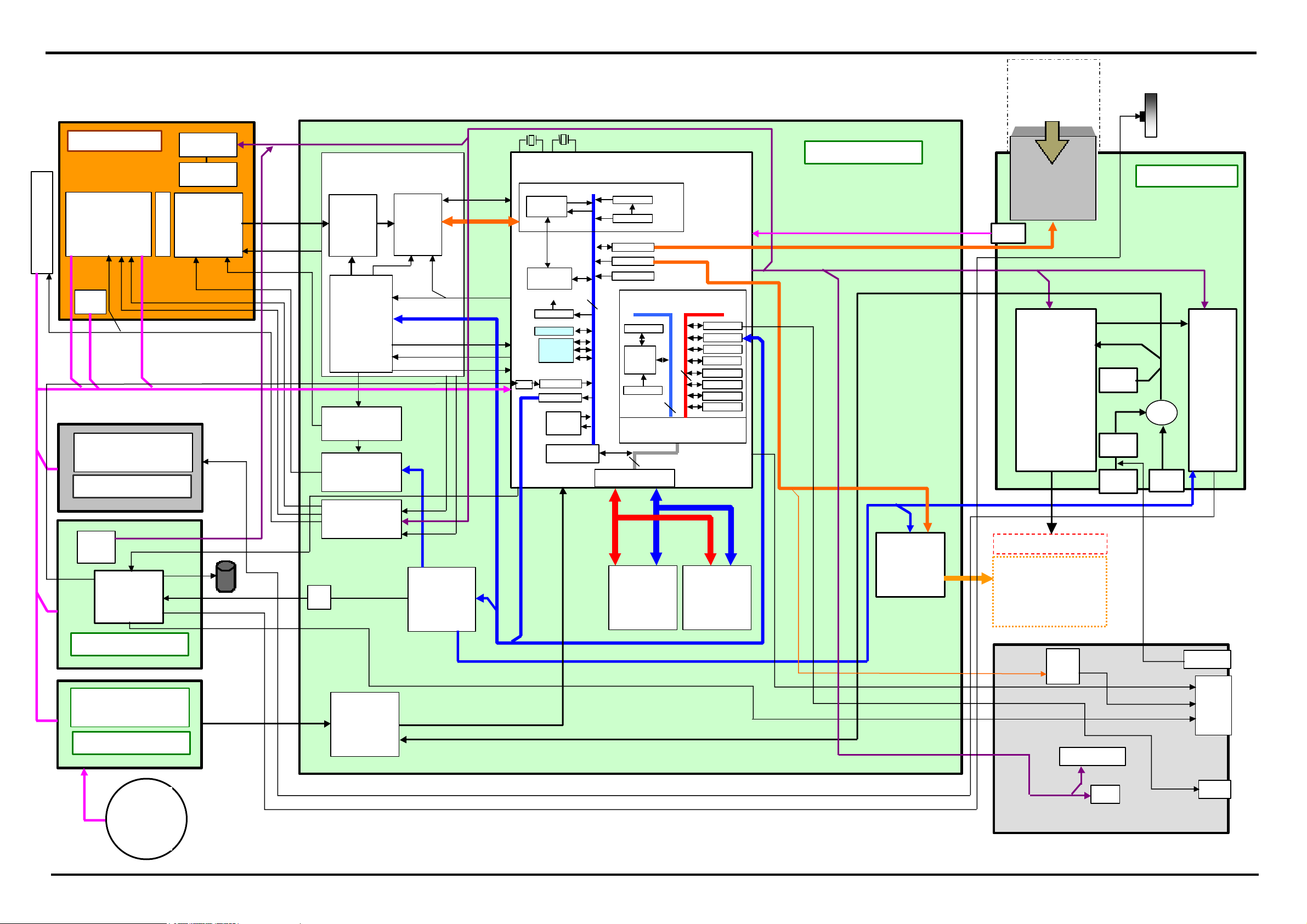
FinePix F601 Zoom(U/E/EG) SERVICE MANUAL
(UCS)
F
AVD, AHD, FLD1, ADCLK
NP-60
V
H
H1~H8 RG
Smart Media
(3.3V Only)
2M, 4M, 8M,16M,
32M, 64M, 128M
3.Schematic
3-4. Basic block diagram
LENS CONST
LENS COVER
Super EBC FUJINON
Optical' 3 zoom lens
Barrier open SW
POP SW
Zoom position
POWER SW / DISP SW
LED x 6 / Release SW DISP SW
MODE ST UNIT
Battery
(Back up)
Focus HP
IC401
(AUDIO_AMP)
LED_R/B
FINDER
O.
Super CCD
L
1/1.7inch
3.3 million pixels
P
Various Control Pulse
Detect function
MIC
CCD_IN
IC109 (SCS3A)
ANALOG
BLOCK
Various
TG
(PROGRAMABLE)
IC105
(V-DRV)
IC101
(OFD/RG BIAS)
IC113 (ZOOM/SHUTT/
IRIS BIAS-DRV)
LPF
Various
ADCLK
A/D
(12bit)
X_TRG
X_RDY
RESET
DL, CLK, LD
24M
STROBO
FM
CAM1~4
IC103
(8ch EVR D/A)
STB, RW
V_RST
H_RST
OCONT
(24.375)
DEBUG I/F
CPU CORE
J- cache 8k
??????(75MH)
Various Control
32?
Bus control
BSELC
DMAC
A<9,10,18-29>
CPU (75Mz)
32b
SDRAMC
SYSC
ADDRESS BUS
IC208
(F_ROM)
(16Mb)
USB
SIO
WDT
MFT
ICU
ADC
PORT
CLKC
D<0-15>
A<0-19>
MAIN PWB ASSY
SPEAKER
SSFDC SOCKET
DCST PWB UNIT
(24P)
CN901
DR_SW
Various Control
DC/DC_Control
IC603
(DC/DC Control)
CPU_UNREG
3.3V
5.0V
CHARGE
CCD16V, -8V
LCD8.5V
SW
BL
OTHERS
R/G/B
IC553
(LCD Control)
BL LED
LCD Monitor
FUSE
DC_JACK
GSEL, G_No
1.5 inches
Low-temperature polysilicon TFT
110,000 pixels
IC802
(STRB
Control)
Image bus (75Mhz)
1394
MPEG2
Audio(A/D)
JPEG
Image bus I/F
X’TAL 48M X’TAL 24,575
DATA BUS
CCDIF
MEDIA
TFDC
32b
???????
AUTO
ENCD
M32R/E CPU
CPU I/O(75Mhz)
32b
I/O Buffer
IBFC
YCIF
YCPRO
BITMAP CG
A/D
Audio(A/D)
Audio(Serial)
IC206 (SDRAM)
(256Mb)(x 32)
SUB PWB ASSY
POWER SW / DISP SW
LED x 6
LED PWB ASSY
8 KEY
CAM/PB SW
L/R/U/D SW
OK SW
IC353
(POWER_ON)
VBS
75 ohm
DRV
AV_DET
DC_IN
AUDIO
VIDEO
OUT
Power SW
LED
USB
Cradle IF
19
20
FinePix F601 Zoom(U/E/EG) SERVICE MANUAL
3.Schematic
3-5. Overall Connections
BARRIER
MOTOR
CCD
LENS CONST
CN151
HEAD
SUB PWB ASSY
CN401
Board to Board
CN202 CN152
SPEAKER
CN501
LCD
FPC
CN103
FPC
CN102 CN11
MAIN PWB ASSY
CN101
SSFDC
Board to Board
CN603
8 DIRECTION
KEY ASSY
MIC
CN51
CN606
CN601
CN901
J602
J601
DC_IN
PC
AC V5HS
CN52
LED PWB ASSY
FPC
CN604
DCST PWB UNIT
CN602
BATT_IN
NP-60
 Loading...