

FUJIFILM FinePix A204 Service Manual
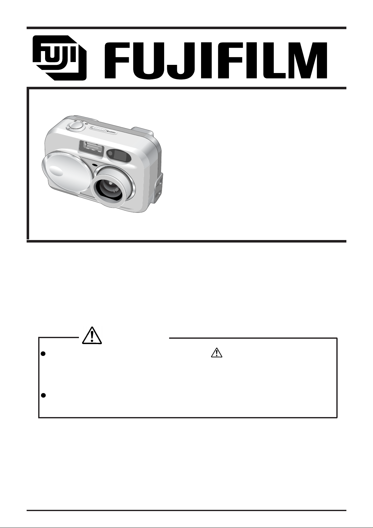
DIGITAL CAMERA
FinePix A204
SERVICE MANUAL
EU/EG/GE/AS-Model
WARNING
THE COMPORNENTS IDENTIFIED BY THE MARK “ ” ON THE SCHEMATHIC
DIAGRAM AND IN THE PARTS LIST ARE CRITICAL FOR SAFETY.
PLEASE REPLACE ONLY BY THE COMPONENTS SPECIFIED ON THE SCHEMATHIC
DIAGRAM AND IN THE PARTS LIST.
IF YOU USE WITH PART NUMBER UN-SPECIFIED, IT MAY RESULT IN A FIRE AND AN
ELECTORICAL SHOCK.
Ref.No.:ZM00457-101
FUJI PHOTO FILM CO.,LTD.
Printed in Japan 2002.8 (T.S.)
SAFETY CHECK-OUT
After correcting the original problem, perform the following safety
check before return the product to the costomer.
FinePix A204 (EU/EG/GE/AS) SERVICE MANUAL
1. Check the area of your repair for unsoldered or poorly
sol dered connections. Check the entire board sur
face for solder splasher and bridges.
2. Check the interboard wiring to ensure that no wires
are pinched or contact high-wattage resistors.
3. Look for unauthorized replacement parts, particu
larly tran sistors, that were installed during a previ
ous repair. Point them out to the customer and rec
ommend their replacement.
4. Look for parts which, though functioning, show obvi
ous signs of deterioration. Point them out to the cus
tomer and recommend their replacement.
5. Check the B + voltage to see it is at the values specified.
6. Make leakage - current measurements to determine
that exposed parts are acceptably insulated from the
supply circuit before returning the product to the customer.
7. CAUTION: FOR CONTINUED
PROTECTION AGAINST FIRE
HAZARD, REPLACE ONLY WITH
SAME TYPE 2.5 AMPERES 125V
FUSE.
2.5A125V
2.5A125V
8.
RISK OF FIREREPLACE FUSE
AS MARKED
WARNING!
HIGH VOLTAGE
ATTENTION: AFIN D'ASSURER
UNE PROTECTION
PERMANENTE CONTRE LES
RISQUES D'INCENDIE,
REMPLACER UNIQUEMENT
PAR UN FUSIBLE DE MEME,
TYPE 2.5 AMPERES, 125
VOLTS.
WARNING:
TO REDUCE THE ELECTRIC
SHOCK, BE CAREFUL TO
TOUCH THE PARTS.

FinePix A204 (EU/EG/GE/AS) SERVICE MANUAL
CONTENTS
Table of Contents
1. General
1-1. Product specification ...................................................... 4
1-2. Explanation of Terms...................................................... 6
1-3. Names of External Components ................................... 7
2. Disassembly
2-1.Names of internal Components ...................................... 8
2-2.Removing CABI REAR ASSY ......................................... 9
2-3.Removing LCD ASSY / LCD FRAME. ........................... 1 0
2-4.Removing MAIN PWB CONST. ...................................... 11
2-5.Removing LENS CONST. ............................................... 11
2-6.Removing ST PWB CONST. ........................................... 11
2-7.Removing Removing BATTERY HOLDER. .................. 12
2-8.Removing LENS BARRIER ASSY. ................................ 13
3.Schematic
3-1.Cautions ............................................................................. 14
3-2.Basic block name and function explanation ................. 14
3-3. Explanation of Main Block Functions ........................... 1 5
3-3-1. Technology Outline .............................................. 15
3-3-2. Explanation of Block Functions ......................... 15
3-4. Block Diagram ................................................................. 16
3-5. Overall Connections ....................................................... 1 7
3-6.Board mounting diagram ................................................. 18
3-6-1.Printed wiring board of ST PWB CONST. ......... 18
3-6-2.Printed wiring board of MAIN PWB ASSY. ....... 19
5. Inspection
5-1. Required Measuring Equipment .................................... 45
5-2. Connection of Measuring Equipment ........................... 4 5
5-3. Inspection and Factory Settings ................................... 45
6.Parts List
6-1.Packing and Accessories ................................................ 4 7
6-1-1.Packing and Accessories(EU model) ................. 4 7
6-1-2.Packing and Accessories(EG model) ................ 48
6-1-3.Packing and Accessories(GE model) ................ 49
6-1-4.Packing and Accessories(AS model) ................. 50
6-2.Cabinet F block (EU/EG/GE/AS model) ........................ 51
6-3.Cabinet R block (EU/EG/GE/AS model) ....................... 52
6-4.Electrical Parts (EU/EG/GE/AS model) ........................ 53
7. Appendix
7-1.List of Related Technical Updates Issued .................... 54
4.Adjustment
4-1.Important point Adjustment when Replacing Major Parts .. 20
4-2.The order of adjustment when Major Parts are replaced ... 20
4-3.Measuring Instruments Used .......................................... 20
4-4.Use Jig list ......................................................................... 20
4-5.Measuring Intrument and Jig Connection Diagram ..... 21
4-6. Setup for adjustment ...................................................... 21
4-7.Various downloading software
decompressions,preservation methods, and notes ........... 22
4-8.Install the DSC jig driver and the PC adjustment software. 23
4-9. Setting up the Adjustment Software ............................. 24
4-10. Starting the Adjustment Software ............................... 26
4-11.[F2] Zoom adjustment, CCD/Zoom data input ........... 29
4-12.[F5] CAM Adjustment .................................................... 31
4-13.[F6].AF adjustment ........................................................ 34
4-14.[F1] Battery Voltage Adjustment .................................. 36
4-15 [F3] LCD Adjustment ..................................................... 38
4-16.[F7] Flash Adjustment ................................................... 39
4-17.[F12] End Setting ........................................................... 41
4-18 [F8] Firmware Download ............................................... 44
3
1. General
FinePix A204 (EU/EG/GE/AS) SERVICE MANUAL
1. General
1-1. Product specification
System
Model Digital camera FinePix A204
Number of effective pixels 2.0 million
CCD Sensor 1/2.7-inch square pixel CCD
Total number of pixels: Approx. 2.11 million
Image quality 1600 x 1200 pixels (1.92 million pixels)/1280 x 960 pixels/640 x 480 pixels
File format Still image: JPEG (Exif Ver. 2.2), DPOF-compatible
Movie: AVI format, motion JPEG
* Design rule for Camera File system compliant
Viewfinder Real image optical; Frame coverage: 80%
Lens Fujinon optical 3x zoom lens
Aperture F3.5/F8.7 (automatically selected)
Storage media xD-Picture Card
Focus distance f = 6 mm-18 mm (equivalent to 38 mm-114 mm on a 35 mm camera)
Exposure control 64 zones TTL metering, Program AE (exposure compensation available in Manual mode)
Sensitivity Equivalent to ISO 100
White balance Auto (7 positions selectable in Manual mode)
Focal range Normal: Approx. 80 cm (2.6 ft.) to infinity
Macro: Approx. 10 cm (3.9 in.) to 80 cm (2.6 ft.)
Shutter speeds Variable-speed, 1/2 to 1/1000 sec. (combined with mechanical shutter)
Flash (Auto flash using flash control sensor)
Effective range: Wide-angle Approx. 0.2 m-3.0 m (0.6 ft.-9.8 ft.)
: Telephoto Approx. 0.8 m-3.0 m (2.6 ft.-9.8 ft.)
Flash modes: Auto, Red-Eye Reduction, Forced Flash, Suppressed Flash, Slow Synchro
LCD monitor 1.5-inches, 55,000-pixels D-TFD
Self-Timer 10 sec. timer clock
Standard number of available shots/recording time per xD-Picture Card
Quality Mode 2M - F 2M - N 1M 0.3M
Number of recorded pixels 1600 x 1200 1280 x 960 640 x 480 320 x 240 160 x 120
Image Data Size Approx.620KB Approx.390KB Approx.320KB Approx.130KB - -
DPC-16 (16 MB) 25 39 49 122 Approx. 94 sec. Approx. 5.0 min.
DPC-32 (32 MB) 50 79 99 247 Approx. 191 sec. Approx. 10.1 min.
DPC-64 (64 MB) 101 159 198 497 Approx. 6.4 min. Approx. 20.2 min.
DPC-128 (128MB) 204 319 398 997 Approx. 12.9 min. Approx. 40.6 min.
Input/Output Terminals
DC IN 3V (Power input) Special AC Power Adapter AC-3V
socket
(USB) socket USB (1) for image data output with a personal computer
4

FinePix A204 (EU/EG/GE/AS) SERVICE MANUAL
1. General
Power Supply and Others
Power supply Use one of the following:
* 2AA-size alkaline batteries
* 2AA-size Ni-MH (nickel metal hydride) batteries (provided)
* AC Power Adapter AC-3V (optional)
No. of available shots using battery (battery life)
Battery Type With LCD monitor ON With LCD monitor OFF
Alkaline batteries Approx. 150 frames Approx. 250 frames
Ni-MH batteries HR-3UF 1700 mAh Approx. 250 frames * Approx. 400 frames *
(Condition: Power saving mode ON, with fully charged battery (Ni-MH))
This indicates the number of available frames shot consecutively at room temperature with a flash use rate of 50%.
Note that these figures may vary depending on the ambient temperature and the amount of charge in the battery.
The number of available shots or available shooting time will be lower in cold conditions.
o
Conditions for use Temperature: 0
humidity or less (no condensation)
Camera dimensions 100.4 mm x 65 mm x 51.7 mm/4.0 in. x 2.6 in. 5 2.0 in.
(W x H x D) (not including accessories and attachments)
Camera mass (weight) Approx. 185 g/6.5 oz (not including, batteries and xD-Picture Card)
Mass (weight) Approx. 240 g/8.5 oz (including batteries and xD-Picture Card)
for photography
Accessories
Optional Accessories
16 MB, xD-Picture Card (1) Supplied with: Anti-static case (1)
LR6 AA-size alkaline Batteries (2)
Hand strap (1)
USB Interface Set (1)
* CD-ROM: Software for FinePix SX (1)
* USB cable with Noise Suppression core (1)
Owner's Manual (1)
xD-Picture Card
DPC-16 (16MB)/DPC-32 (32MB)/DPC-64 (64MB)/DPC-128 (128MB)
AC Power Adapter AC-3V
FUJIFILM Rechargeable Battery 2HR-3UF
FUJIFILM Battery charger with Battery BK-NH (with Euro type or UK type plug)
SC-FX26
DPC-R1 Image Memory Card Reader
* Compatible with Windows 98/98 SE, Windows Me, Windows 2000 Professional, Win-
dows XP or iMac, Mac OS 8.6 to 9.2.2, Mac OS X (10.1.2 to 10.1.5) and models that
support USB as standard.
* Compatible with SmartMedia of 3.3V, 4MB to 128MB.
DPC-AD PC Card Adapter
* Compatible with SmartMedia of 3.3V, 2MB to 128MB.
C to +40oC (+32oF to +104oF); 80%
5

1. General
FinePix A204 (EU/EG/GE/AS) SERVICE MANUAL
1-2. Explanation of Terms
DPOF: Digital Print Order Format
DPOF is a format used for recording information on a storage media (image memory card, etc.)
that allows you to specify which of the frames shot using a digital camera are printed and how
many prints are made of each image.
EV: A number that denotes Exposure Value. The EV is determined by the brightness of the subject
and sensitivity (speed) of the film or CCD. The number is larger for bright subjects and smaller
for dark subjects. As the brightness of the subject changes, a digital camera maintains the
amount of light hitting the CCD at a constant level by adjusting the aperture and shutter speed.
When the amount of light striking the CCD doubles, the EV increases by 1. Likewise, when the
light is halved, the EV decreases by 1.
JPEG: Joint Photographics Experts Group
A file format used for compressing and saving color images. The compression ratio can be
selected, but the higher the compression ratio, the poorer the quality of the expanded image.
Motion JPEG: A type of AVI (Audio Video Interleave) file format that handles images and sound as a single file.
Images in the file are recorded in JPEG format. Motion JPEG can be played back by QuickTime
3.0 or later.
PC Card: A generic term for cards that meet the PC Card Standard.
PC Card Standard: A standard for PC cards determined by the PCMCIA.
PCMCIA: Personal Computer Memory Card International Association (US).
White Balance: Whatever the kind of the light, the human eye adapts to it so that a white object still looks white.
On the other hand, devices such as digital cameras see a white subject as white by first adjust-
ing the color balance to suit the color of the ambient light around the subject. This adjustment
is called matching the white balance. A function that automatically matches the white balance is
called an Automatic White Balance function.
6
FinePix A204 (EU/EG/GE/AS) SERVICE MANUAL
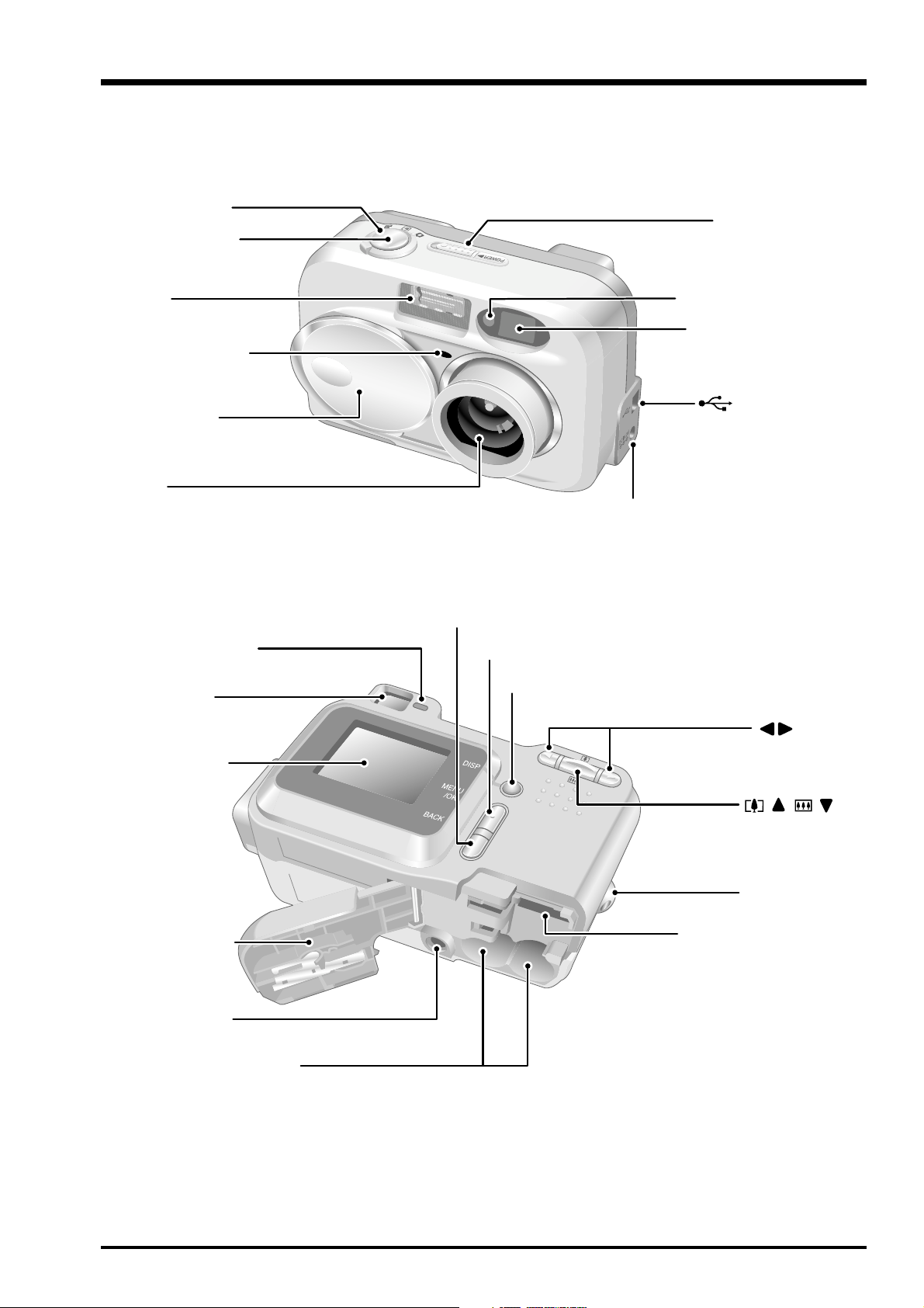
1-3. Names of External Components
1. General
Mode Switch
Shutter button
Flash
Self-timer lamp
Lens cover
Lens
Viewfinder lamp
POWER switch
Flash control sensor
Viewfinder window
(USB) socket
DC IN 3V (Power input) socket
BACK button
MENU/ OK button
Viewfinder
LCD monitor
Battery cover
Tripod mount
Battery compartment
DISP button
button
( ) ( )/
Zoom button
Strap mount
xD-Picture Card slot
7
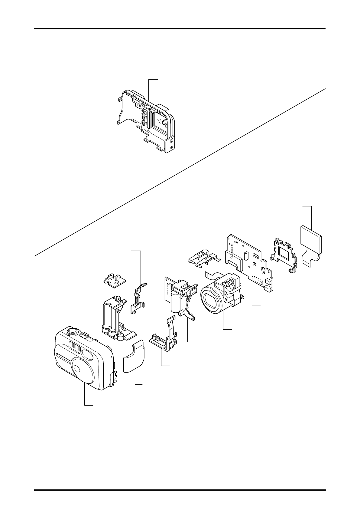
2. Disassembly
2. Disassembly
2-1.Names of internal Components
FinePix A204 (EU/EG/GE/AS) SERVICE MANUAL
CABI REAR ASSY
RSW PWB ASSY
BATTERY HOLDER
LCD ASSY
LCD FRAME
FRAME L
MAIN PWB ASSY
LENS CONST
DCST PWB ASSY
FRAME R
BATTERY LID ASSY
CABI FRONT ASSY
8
FinePix A204 (EU/EG/GE/AS) SERVICE MANUAL
2-2.Removing CABI REAR ASSY
Remove in the order indicated by circled numbers.
<Step1>
2. Disassembly
1
<Step2>
(1) Remove five screws.
(2) Battery lid is opened.
1
2
1
(3) CABI REAR ASSY is removed in the direction
of the arrow.
33
9
2. Disassembly
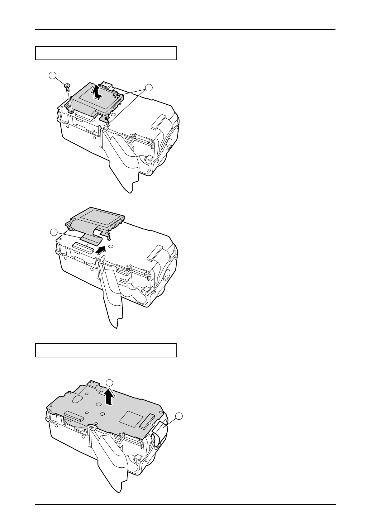
2-3.Removing LCD ASSY / LCD FRAME.
Remove in the order indicated by circled numbers.
<Step1>
1
FinePix A204 (EU/EG/GE/AS) SERVICE MANUAL
<Step2>
2
3
(1) Remove one screws.
(2) Remove the hook of LCD FRAME (two places),
and raise LCD ASSY in the direction of the arrow.
(3) Remove the lock of CN501, and remove LCD
ASSY/LCD FRAME to the direction of the arrow.
2-4.Removing MAIN PWB CONST.
Remove in the order indicated by circled numbers.
<Step1>
2
10
(1) Remove CN801.
(2) Remove MAIN PWB CONST in the direction
of the arrow.
1

FinePix A204 (EU/EG/GE/AS) SERVICE MANUAL
2-5.Removing LENS CONST.
Remove in the order indicated by circled numbers.
2. Disassembly
<Step1>
1
4
2
3
2-6.Removing ST PWB CONST.
Remove in the order indicated by circled numbers.
<Step1>
1
1
(1) Remove two screws.
(2) Remove solder.
(3) Remove CN701.
(4) Remove MAIN PWB ASSY in the direction of the
arrow, and separate with LENS CONST.
(1) Peel off the UL tape, and do discharge.
<Step2>
2
(2) Remove three screws.
(3) Remove CN852.
(4) Remove ST PWB CONST in the direction
4
1
3
of the arrow.
* Reassemble BATTERY HOLDER ASSY in the
state of the power lever off.
11

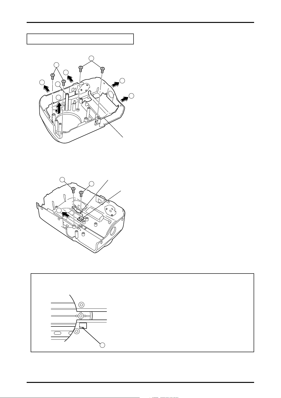
2. Disassembly
2-7.Removing Removing BATTERY HOLDER.
Remove in the order indicated by circled numbers.
<Step1>
1
2
FinePix A204 (EU/EG/GE/AS) SERVICE MANUAL
(1) Remove one screws.
(2) Remove FRAME R and FRAME L.
2
<Step2>
4
3
5
(3) Change MODE DIAL to the camera mode.
(4) Remove two screws.
(5) Remove BATTERY HOLDER in the direction
of the arrow.
12
FinePix A204 (EU/EG/GE/AS) SERVICE MANUAL
2-8.Removing LENS BARRIER ASSY.
Remove in the order indicated by circled numbers.
<Step1>
1
1
2
2
A
B
3
INNER CABI
2. Disassembly
(1) Four screws are removed.
(2) Have the part of (A) by the finger, and expand
CABI FRONT in the direction of the arrow(2).
And, remove INNER CABI in the direction of (B).
(3) Expand CABI F in the direction of (3),
and remove the whole of INNER CABI.
3
* INNER CABI is installed in CABI FRONT with the
hook in four places.
<Step2>
6
4
* How to install BARIA HOOK
BARRIER HOOK
5
BARRIER GUIDE
1. Close LENS BARRIER.
2. Set [BARIA hOOK] to the position of C, and stop the screw.
(4) Close LENS BARRIER.
(5) Remove the screw, and remove BARRIER GUIDE.
(6) Remove the screw, and remove the BARRIER hook
in the direction of the arrow.
C
13

3.Schematic
FinePix A204 (EU/EG/GE/AS) SERVICE MANUAL
3.Schematic
3-1.Cautions
<Caution when replaceing chip (leadless) parts.>
* Do not re-use the removed parts, but use new parts.
Be careful that the negativ side of the tantalum capacitors are susceptible to heat.
* Voltage indications are omitted for capacitors other than chemical and tantalum capacitors
with a dielectric strength of 50 V or less.All units are uF (p shows pF).
* Chip resistors without indication are 1/10 W.
* k=1000
* Variable resistors and semi-variable resistor are abbreviated the specification of B characteristic.
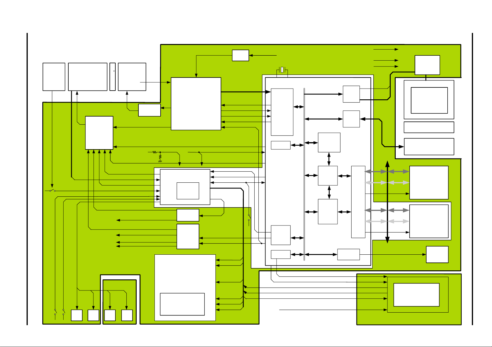
3-2.Basic block name and function explanation
Board Name Block name Function
LENS CONST CCD BLOCK * CCD output
MAIN PWB ASSY CAM BLOCK * Analog to digital conversion of CCD output (IC103)
ST PWB CONST FlashBLOCK * Flash luminescence processing(IC702)
RSW PWB ASSY MSW BLOCK * Operation SW (power supply/mode/shutter)
, M=1000 k
* CCD driver (IC102)
MOTOR BLOCK * Zoom/AF/shutter/iris drive (IC703)
PROCESS BLOCK * USB communication (IC304)
* System control/SW detection management (IC304)
LCD BLOCK * LCD control driver (IC502)
DCDC BLOCK * Each power supply generation(IC401)
14

FinePix A204 (EU/EG/GE/AS) SERVICE MANUAL
3.Schematic
3-3. Explanation of Main Block Functions
3-3-1. Technology Outline
The FinePix 2650/A204 incorporates two new ICs - a intelligent highly integrated image processor IC (WCS:304)
The intelligent highly integrated image processor IC (WCS:304) is equivalent to the image signal processing IC (VCS:
IC209) incorporated in previous models of the FinePix 2600Zoom, however it provides a dramatic reduction in imaging/
playback interval time, and improved S/N ratio and image sharpness.
Time required for transfer of software via the USB interface is reduced due to the use of the WCS internal buffer.
3-3-2. Explanation of Block Functions
(1) CCD signal processing/Imaging circuit (CCD block) (CAM block)
The analog video signal from the CCD (1/2.7, 2,000,000 pixels, square pixel CCD) is pseudo color compensated
(CDS), optimally interpolated (CDS), amplified (AGC), and signal is mixed (CDS) in the single-chip CSP_IC (IC103:
SCS3A), and converted (A/D) to a 12-bit digital signal (CSP_IC = Chip Size Package IC). The CSP_IC incorporates
the TG/SSG function previously supported with a separate IC into a single IC. The converted digital signal is sent to
the intelligent highly integrated image processor IC (WCS:304).
This block contains a horizontal/vertical drive IC (IC102) to drive the CCD.
(2) Motor Circuit (MOTOR block)
The signal processing system IC (WCS:304) receiving the commands from the various switches controls the AF
MOTOR DRV (IC703), SHUTTER DRV (IC703), ZOOM MOTOR DRV (IC703), and IRIS MOTOR DRV (IC703), and controls each motor with the relevant driver.
(3) Image Signal Processing (PROCESS block)
(Input data from CCD)
The 12-bit digital image data (1H equivalent) from the imaging block (CCD_CAM block) is sent to the intelligent
highly integrated image processor IC (WCS:304), buffered in its internal buffer, and converted to 32-bit (128-bit) data
(CCD raw data). The 32-bit image data (CCD raw data) is saved in the 32 Mbyte SDRAM (IC305) via the image signal
processor IC I/O bus. A single frame (1600 pixels x 1200 lines) of image data is held temporarily in the SDRAM. The
32-bit image data in the intelligent highly integrated image processor IC (WCS:304) is processed in the AUTO math
processor, and sent to the SCS3A_IC (IC103) in the CAM block to obtain the optimum AE, AWB, and AF.
(Recording on xD-Picture Card)
The image data saved in the SDRAM (IC305) is sent to the signal processing block one line at a time via the intelligent
highly integrated image processor IC (WCS:304) I/O bus. It is then unpacked (ie. converted from 32-bit to 12-bit) in the
signal processing block, and pre-processed using digital clamping, g compensation, and conversion of R, G, and B
data to 12-bit to 8-bit. Each 8-bit digital R, G, and B signal is then subject to YC processing to produce a Y:Cb:Cr ratio of
4:2:2, and each 8-bit Y, Cb, and Cr image data is then sent again to the internal buffer. Each 8-bit Y, Cb, and Cr signal is
then sorted in the internal buffer to facilitate DCT compression, and recorded in the xD-Picture Card via the JPEG
processor and media controller.
(Image replay from xD-Picture Card)
Compressed image data from the xD-Picture Card is sent to the intelligent highly integrated image processor IC
(WCS:304) as eight bit image data, and finally sent to the SDRAM (IC305) via the media control unit, DMA unit, and
internal bus control unit. The image data temporarily stored in the SDRAM (IC305) is then returned to the intelligent
highly integrated image processor IC (WCS:304), and then sent to the image processing block via the media
controller and JPEG processor. Each 8-bit Y:Cb:Cr image signal is then converted to 8-bit R, G, and B signals,
simultaneously superimposed on text display signals, and sent to the LCD block.
The imaging adjustment data is stored in the WCS (IC304).
(4) Power supply (DCDC block)
The power supply circuit on the DC board is used to generate the 1.5V[WCS(IC304)], 3.4V[WCS(IC304), SDRAM
(IC305), RSW PWB, STRB], 3.4V[EVR(IC302/303)], CAM_3. 4V (CAM_BLOCK), LCD_3.4V(LCD), MOT_3.4V
(MOTOR_BLOCK), MOT_5.25V (MOTOR_BLOCK), -8.0V(CCD), 15.5V(CCD, LCD), and UNREG voltages.
15
DC BLK
SCS3A
WCS IC304
CCDLD
OCONT, VRESET
1.5inch
55,000 pixels
D-TFD
LCD
LCD
DRIVER
HI, VI, ADCLK,FI
CCDDT[9:0]
18MHz
X'tal
CISC
EVR2
V DRIVER
IC102
CCD
2M
Bayer
O
L
P
F
LENS
x 3 ZOOM
Timer
MOTOR DRV.
IRIS DRV.
SHUT DRV.
FOCUS DRV.
IRIS2
Z_HP, Z_PLS
FOCUS_HP
FMA1, FMA2, FMB1, FMB2
SHUT1, SHUT2, IRIS1
DC/DC IC
CCDOUT
48MHz
xD-Picture Card
BL(LED)
DRAM
8MByte
FLASH ROM
1MByte
USB
D+, D-, VBUS, TRON
BL_ON
CAM_ON
LCD_ON
CARD_ON
STRB BLK
CONTROL IC
F_LON
Z_LON
STRB_COK
STRB_CC
STRB_FULL
TG_SY
STRB_SY
EVR_LD
CAMCLK
FMPS
GSEL, V_TH, STRB_CHG
LCD_CONT
MEDIA
LCD
LCDCLK
LCDHD
LCDVD
LCDDATA
[7:0]
IBUF
SEL
USB
CPU
Core
Memory
Ctrl
Local
BUS
Memory
Ctrl
Serial
JPEG
TIMER
LED
R
LED
B
LED
ST
STRB_DIS
DR_SW
IRIS_SPD,
GSEL, V_TH
LCD_CONT
PWR_SW, S1/S2
KEY1, KEY2, MODE1
LENS
Barrier
BAR1,BAR2
BAR_OPEN, BAR_CLOSE
Buzz
er
VDET
BAT_V
LCD_UNI_BR
LCD_UNI_BR
from EVR
from EVR
to STRB
to LCD
CS
SI, SO, SCLK
SO, SCLK
SI, SO, SCLK
SIO2
SIO1
B_LON
EVR1
to STRB
STRB_CHG
ZMPS
TELE, WIDE
from CISC
LCD BLK
EVR_LD
SO, SCLK
from CISC
MCM
IC602
IC401
IC502
IC103
IC703
IC302
IC303
IC305
MAIN PWB ASSY
ST PWB CONST
ST PWB
FinePix A204 (EU/EG/GE/AS) SERVICE MANUAL
3.Schematic
3-4. Block Diagram
16
ST PWB CONST
PC
CN302
CN851 CN801
FFC
MAIN PWB ASSY
N
FinePix A204 (EU/EG/GE/AS) SERVICE MANUAL
3-5. Overall Connections
CN301
CN701
FPC
XD-Picture
Card
17
CN852
FFC
CN951
RSW PWB ASSY
3.Schematic
J401
CN501
FPC
LENS CONST
BATT.
LCD ASSY
DC_IN
 Loading...