

FUJIFILM FinePix A101 SHEMATICS

DIGITAL CAMERA
FinePix A101
SCHEMATICS
U/E/EG-Model
WARNING
THE COMPONENTS INDENTIFIED BY MARK IN THE PARTS LIST SHOULD BE REPLACED
ONLT BY THE COMPONENTS SPECIFIED IN THE PARTS LIST.
RISK OF FIRE AND ELECTRIC SHOCK.
Ref.No.:ZM00374-200
FUJI PHOTO FILM CO., LTD.
Printed in Japan 2001.8(NT)
SAFETY CHECK-OUT
After correcting the original problem, perform the following
safety check before return the product to the costomer.
FinePix A101 (U/E/EG) SCHEMATICS
1. Check the area of your repair for unsoldered or
poorly soldered connections. Check the entire
board surface for solder splasher and bridges.
2. Check the interboard wiring to ensure that no
wires are “pinched” or contact high-wattage
resistors.
3. Look for unauthorized replacement parts, particularly transistors, that were installed during a
previous repair. Point them out to the customer
and recommend their replacement.
4. Look for parts which, though functioning, show
obvious signs of deterioration. Point them out to
the customer and recommend their replacement.
5. Caution:
For continued protection against
2.5A 125/250V
2.5A 125/250V
RISK OF FIREREPLACE FUSE
AS MARKED
fire hazard, replace only with same
type 2.5 amperes 125/250 volts
fuse.
Attention:
Afin d’assurer une protection
permanente contre les risques
d’incendie, remplacer uniquement
par un fusible de meme, type 2.5
amperes, 125/250 volts.
6. Warning:
To reduce the electric shock, be
WARNING!
HIGH VOLTAGE
careful to touch the parts.
2

FinePix A101 (U/E/EG) SCHEMATICS
TABLE OF CONTENTS
TABLE OF CONTENTS
1. Notes on Schematics Diagrams .....................................4
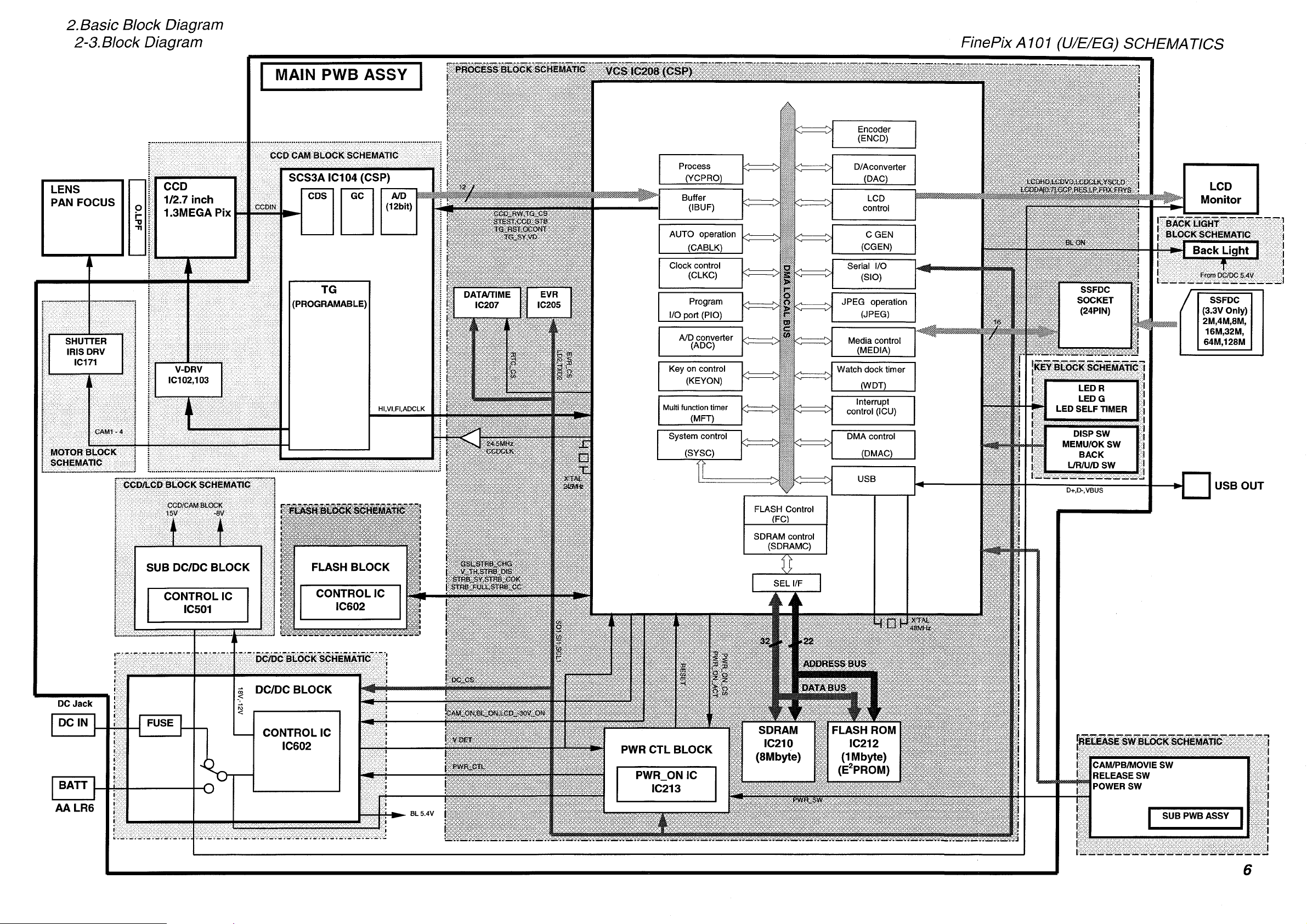
2. Basic Block Diagram
2-1.Overview of Functions of Each Circuit ............................................... 4
2-2.Description of Block Functions ........................................................... 5
2-3.Block Diagram...................................................................................... 6
3.Schematics
3-1.MAIN PWB ASSY
3-1-1.MAIN PWB ASSY Component Location (A) ............................... 7
3-1-2.MAIN PWB ASSY Component Location (B) ............................... 8
3-1-3.Motor Block Schematics .............................................................. 9
3-1-4.CCD CAM Block Schematics..................................................... 10
3-1-5.Process Block Schemaics ......................................................... 11
3-1-6.CCD/LCD Block Schematics .....................................................12
3-1-7.Flash Block Schematics ............................................................. 13
3-1-8.DC/DC Block Schematics .......................................................... 14
3-1-9.Back Light Block Schematics .................................................... 15
3-1-10.Key Block Schematics.............................................................. 16
3-2.SUB PWB ASSY
3-2-1.SUB PWB ASSY Component Location ..................................... 17
3-2-2.Release SW Block Schematics .................................................18
page
3

1.Notes on Schematics Diagrams
FinePix A101 (U/E/EG) SCHEMATICS
1.Notes on Schematics Diagrams
Other neccessary notes are shown in each block.
1-1.Cautions
Caution when replaceing chip (leadless) parts.
* Do not re-use the removed parts, but use new parts.
Be careful that the negativ side of the tantalum capacitors are susceptible to heat.
* Voltage indications are omitted for capacitors other than chemical and tantalum capacitors with a dielectric strength of
50 V or less.All units are uF (p shows pF).
* Chip resistors without indication are 1/10 W.
* k=1000
* Variable resistors and semi-variable resistor are abbreviated the specification of B characteristic.
, M=1000 k
2.Basic Block Diagram
2-1.Overview of Functions of Each Circuit
Board Name Circuit Diagram Name Circuit Functions
MAIN PWB ASSY Motor block schematics Shutter iris block circuit
CCD / CAM block schematics A/D conversion of CCD output signal block circuit
Prosess block schematics Syscon, Process(VCS) / SDRAM / Flash ROM /
Power control block circuit
CCD / LCD block schematics CCD, LCD panel power supply block circuit
Flash block schematics Flash control block circuit
DC/DC block schematics Power supply / Control of Flash / LCD back light
inverter circuit
Back light block schematics LCD back light block circuit
Key block schematics Control switch circuit
SUB PWB ASSY Release SW block schematics Cam, PB, Movie, Release, Power switch circuit
4

FinePix A101 (U/E/EG) SCHEMATICS
2.Basic Block Diagram
2-2.Description of Block Functions
2-2-1.Overview of New Technology
Basic block functions are almost the same as those of the FinePix1300. Differences in block function from those of the
FinePix1300 are the following one points.
1. The noise of low brightness is decreased without ruining a high luminance resolution by the coring setting according to
brightness by the adoption of new IC (VSC_IC).
2-2-2.Description of the Block Functions in the MAIN PWB UNIT
(1)Description of Camera Circuit Block Functions (CAM BLOCK)
Analog video signals output from CCD (1/2.7", approx. 1.3 million pixels) undergo pseudocolor compensation processing,
applied interpolation processing, amplification, and signal mixing in the SCS3A_IC (IC104: CSP_IC), and thereafter are
converted to 12-bit digital signals. The converted digital signals are sent to the single-chip VCS_IC (IC208: CSP_IC).
(CSP_IC=
(2)Description of the Image Signal Processing Block (PROCESS BLOCK)
Input Data from the CCD
* The 12-bit digital image data (a portion equivalent to 1 H) output from the camera block (CAM BLOCK) is sent to the VCS_IC,
buffer processing is performed in the [Buffer] of this IC, and replacement with 32-bit (16-bit x 2) data is performed. The
replaced 32-bit image data passed through the [DMA Local Bus] in the VCS_IC, then is stored in the SDRAM_IC
(IC210:8Mbyte). Image data equivalent to one frame (1,280pixels x 960lines) is temporarily stored in the SDRAM_IC.
* At the same time, the AE is added in the [AUTO operation] utilizing the 12-bit image data input to the VCS_IC, and required
data for AE and AWB are sent to the SDRAM_IC. The SDRAM_IC, serial data transfer to the SCS3A_IC is performed so that
the appropriate AE and AWB are obtained.
Processing for recording to the SSFDC
The image data stored in the SDRAM_IC is converted from 32-bit data to 12-bit data by the [Buffer] in the VCS_IC, and sent
to the [Process]. In this [Process], the 12-bit image data is converted to respective 8-bit Y and C signals, and the image data
is again sent to the [Buffer]. In the [Buffer], the respective 8-bit Y and C signals are converted to respective 8-bit Y, Y, Cb,
and Cr signals, and are sent to the SDRAM_IC. The image data stored in the SDRAM_IC is compressed by the [JPEG
operation] in the VCS_IC, and is again stored in the SDRAM_IC. The compressed image data is sequentially recorded, via
the [Media control] in the VCS_IC, to the SSFDC.
Playback of Images from the SSFDC
Compressed image data from the SSFDC is sent to the VCS_IC, and is stored, via the [Media control], in the SDRAM_IC.
The compressed image data stored in the SDRAM_IC is expanded by the [JPEG operation], and is again stored in the
SDRAM_IC. The image data after expansion is sent via the [Buffer] to the [Process]. In the [Process], the gain control and
the aperture are processed to the Y and C signals. The image data is sent to SDRAM_IC again. The picture data is dis-
played through [Encorder] -> [D/A converter].
During Movie Imaging Mode
The 12-bit image data from the camera block (CAM BLOCK) passes from the [Buffer] to the [Process] in the VCS_IC. In the
[Process], the 12-bit image data is converted to respective 8-bit Y and C signals, and is sent to the SDRAM_IC. The image
data stored in the SDRAM_IC is compressed by the [JPEG operation] in the VCS_IC, and is again stored in the SDRAM_IC.
The image data after compression is sequentially recorded, via the [Media control] in the VCS_IC, to the SSFDC.
Camera-related adjustment data is stored in the FLASH ROM (IC212).
Chip Size Package IC)
(3)Description of LCD Control Block Functions (LCD CONTROL BLOCK)
The Y and C signals processed in the image signal-processing VCS_IC is output to the LCD panel via [LCD control].
The liquid crystal monitor is D-TFD (1.6" type; 55,000 pixels) method used with FinePix1300.
2-2-3.Description of the Functions of the DCST Circuit Board
The power-supply circuit provided on the MAIN circuit board generates power supplies of -8V/15.5V (CCD drive), 1.5V
(VCS_IC), 3.3V (SCS3A_IC, VCS_IC, SDRAM_IC, ROM_IC, LEDs, and keys), 5.4V (lens drive, flash, and LCD backlight), 5V
(LCD schematic), and so on.
5
 Loading...